Movatterモバイル変換


[0]ホーム

URL:


JP7534654B2 - Laser Light Source - Google Patents

Laser Light Source
Download PDF

Info

Publication number
JP7534654B2
JP7534654B2JP2021566816AJP2021566816AJP7534654B2JP 7534654 B2JP7534654 B2JP 7534654B2JP 2021566816 AJP2021566816 AJP 2021566816AJP 2021566816 AJP2021566816 AJP 2021566816AJP 7534654 B2JP7534654 B2JP 7534654B2
Authority
JP
Japan
Prior art keywords
submount
laser light
light source
lens
diode chip
Prior art date
Legal status (The legal status is an assumption and is not a legal conclusion. Google has not performed a legal analysis and makes no representation as to the accuracy of the status listed.)
Active
Application number
JP2021566816A
Other languages
Japanese (ja)
Other versions
JPWO2021131171A1 (en
Inventor
範宏 出島
英明 竹田
英典 松尾
雅樹 大森
Current Assignee (The listed assignees may be inaccurate. Google has not performed a legal analysis and makes no representation or warranty as to the accuracy of the list.)
Nichia Corp
Original Assignee
Nichia Corp
Priority date (The priority date is an assumption and is not a legal conclusion. Google has not performed a legal analysis and makes no representation as to the accuracy of the date listed.)
Filing date
Publication date
Application filed by Nichia CorpfiledCriticalNichia Corp
Publication of JPWO2021131171A1publicationCriticalpatent/JPWO2021131171A1/ja
Priority to JP2024114842ApriorityCriticalpatent/JP7678389B2/en
Application grantedgrantedCritical
Publication of JP7534654B2publicationCriticalpatent/JP7534654B2/en
Priority to JP2025065735Aprioritypatent/JP2025106518A/en
Activelegal-statusCriticalCurrent
Anticipated expirationlegal-statusCritical

Links

Images

Classifications

Landscapes

Description

Translated fromJapanese

本開示は、レーザ光源に関する。The present disclosure relates to a laser light source.

レーザ光源は、加工、プロジェクタ、および照明器具などの様々な用途に利用される。このようなレーザ光源の典型例は、レーザダイオードチップ、レーザダイオードチップを支持するサブマウント、レーザダイオードチップから出射されるレーザ光の発散角を低減するコリメートレンズを備える(例えば、特許文献1)。レーザダイオードチップ、サブマウントおよびコリメートレンズ等のレンズが半導体レーザパッケージに収容される場合、レーザ光が大きく発散する前に、小さいレンズによってレーザ光をコリメート等することが可能になる。一方で、レーザダイオードチップとレンズとの少しの位置ずれにより、レーザ光源から外部に出射されるレーザ光の光軸の向きが大きくずれる可能性がある。Laser light sources are used for various purposes such as processing, projectors, and lighting equipment. A typical example of such a laser light source includes a laser diode chip, a submount that supports the laser diode chip, and a collimating lens that reduces the divergence angle of the laser light emitted from the laser diode chip (for example, Patent Document 1). When the laser diode chip, the submount, and lenses such as a collimating lens are housed in a semiconductor laser package, it becomes possible to collimate the laser light by a small lens before the laser light diverges significantly. On the other hand, a slight misalignment between the laser diode chip and the lens may cause a large misalignment of the optical axis of the laser light emitted to the outside from the laser light source.

特開2000-98190号公報JP 2000-98190 A

レーザダイオードチップとレンズとの位置ずれが生じにくいレーザ光源が求められている。There is a demand for a laser light source that is less susceptible to misalignment between the laser diode chip and the lens.

本開示のレーザ光源は、一実施形態において、発光層を含む半導体積層構造体と、前記半導体積層構造体を支持する基板と、前記発光層で発生したレーザ光を出射する第1の端面と、前記第1の端面とは反対側の第2の端面と、を有し、前記第1の端面から前記第2の端面までの距離によって共振器長が規定される、端面出射型のレーザダイオードチップと、前記レーザダイオードチップが固着された主平面と、前記レーザダイオードチップの前記第1の端面の両側に位置する一対のレンズ支持部と、前記主平面の反対側に位置する裏面と、を持つサブマウントと、前記一対のレンズ支持部の端面と接合されたレンズと、前記レーザダイオードチップ、前記レンズ、および前記サブマウントを収容する半導体レーザパッケージと、を備え、前記レーザダイオードチップの前記基板よりも前記発光層が前記サブマウントに近い状態で前記レーザダイオードチップが前記サブマウントに固着されており、前記レーザダイオードチップの前記第1の端面は、前記主平面のエッジよりも前記共振器長の方向に突出し、前記一対のレンズ支持部の前記端面は、前記レーザダイオードチップの前記第1の端面よりも前記共振器長の方向に突出する。In one embodiment, the laser light source of the present disclosure includes a semiconductor laminated structure including a light-emitting layer, a substrate supporting the semiconductor laminated structure, an end-emitting type laser diode chip having a first end face for emitting laser light generated in the light-emitting layer and a second end face opposite the first end face, and a cavity length is defined by the distance from the first end face to the second end face, a submount having a main plane to which the laser diode chip is fixed, a pair of lens support parts located on both sides of the first end face of the laser diode chip, and a back surface located on the opposite side of the main plane, and a front surface. the laser diode chip is fixed to the submount with the light emitting layer being closer to the submount than the substrate of the laser diode chip, the first end face of the laser diode chip protruding in the direction of the cavity length beyond an edge of the main plane, and the end faces of the pair of lens support parts protruding in the direction of the cavity length beyond the first end face of the laser diode chip.

本開示によれば、レーザダイオードチップとレンズとの位置ずれが生じにくいレーザ光源を実現することが可能になる。According to the present disclosure, it is possible to realize a laser light source in which misalignment between the laser diode chip and the lens is less likely to occur.

図1Aは、本開示の実施形態1におけるレーザ光源100の構成例を模式的に示す斜視図である。FIG. 1A is a perspective view illustrating a schematic configuration example of alaser light source 100 according to a first embodiment of the present disclosure.図1Bは、図1Aのレーザ光源100の平面構成を模式的に示す図である。FIG. 1B is a diagram showing a schematic planar configuration of thelaser light source 100 in FIG. 1A.図2Aは、図1Aのレーザ光源100から半導体レーザパッケージ40および一対のリード端子50を省略した構成のより詳細を示す斜視図である。FIG. 2A is a perspective view showing in more detail the configuration of thelaser light source 100 in FIG. 1A with thesemiconductor laser package 40 and the pair oflead terminals 50 omitted.図2Bは、図2Aのレーザ光源100を模式的に示す上面図である。FIG. 2B is a top view that diagrammatically illustrates thelaser light source 100 of FIG. 2A.図2Cは、図2Bの構成のYZ平面に平行なIIC-IIC線断面図である。FIG. 2C is a cross-sectional view of the configuration of FIG. 2B taken along line IIC-IIC parallel to the YZ plane.図3Aは、本開示の実施形態1の変形例1におけるレーザ光源110の構成例を模式的に示す斜視図である。FIG. 3A is a perspective view that illustrates a schematic configuration example of alaser light source 110 according to a first modification of the first embodiment of the present disclosure.図3Bは、図3Aのレーザ光源110を模式的に示す上面図である。FIG. 3B is a top view that diagrammatically illustrates thelaser light source 110 of FIG. 3A.図3Cは、図3Bの構成のYZ平面に平行なIIIC-IIIC線断面図である。FIG. 3C is a cross-sectional view of the configuration of FIG. 3B taken along line IIIC-IIIC parallel to the YZ plane.図4Aは、本開示の実施形態1の変形例2におけるレーザ光源120の構成例を模式的に示す斜視図である。FIG. 4A is a perspective view that illustrates a schematic configuration example of thelaser light source 120 according to the second modification of the first embodiment of the present disclosure.図4Bは、図4Aのレーザ光源120を模式的に示す上面図である。FIG. 4B is a top view that diagrammatically illustrates thelaser light source 120 of FIG. 4A.図4Cは、図4Bの構成のYZ平面に平行なIVC-IVC線断面図である。FIG. 4C is a cross-sectional view of the configuration of FIG. 4B taken along line IVC-IVC parallel to the YZ plane.図5Aは、本開示の実施形態1の変形例3におけるレーザ光源130の構成例を模式的に示す斜視図である。FIG. 5A is a perspective view that illustrates a schematic configuration example of thelaser light source 130 according to the third modification of the first embodiment of the present disclosure.図5Bは、図5Aのレーザ光源130を模式的に示す上面図である。FIG. 5B is a top view that diagrammatically illustrates thelaser light source 130 of FIG. 5A.図5Cは、図5Bの構成のYZ平面に平行なVC-VC線断面図である。FIG. 5C is a cross-sectional view of the configuration of FIG. 5B taken along line VC-VC parallel to the YZ plane.図6Aは、本開示の実施形態1の変形例4におけるレーザ光源140の構成例を模式的に示す斜視図である。FIG. 6A is a perspective view that illustrates a schematic configuration example of alaser light source 140 according to a fourth modification of the first embodiment of the present disclosure.図6Bは、図6Aのレーザ光源140を模式的に示す上面図である。FIG. 6B is a top view that diagrammatically illustrates thelaser light source 140 of FIG. 6A.図6Cは、図6Bの構成のYZ平面に平行なVIC-VIC線断面図である。FIG. 6C is a cross-sectional view of the configuration of FIG. 6B taken along line VIC-VIC parallel to the YZ plane.図7Aは、本開示の実施形態1の変形例5におけるレーザ光源150の構成例を模式的に示す斜視図である。FIG. 7A is a perspective view that illustrates a schematic configuration example of alaser light source 150 according to a fifth modification of the first embodiment of the present disclosure.図7Bは、図7Aのレーザ光源150を模式的に示す上面図である。FIG. 7B is a top view that diagrammatically illustrates thelaser light source 150 of FIG. 7A.図7Cは、図7Bの構成のYZ平面に平行なVIIC-VIIC線断面図である。FIG. 7C is a cross-sectional view of the configuration of FIG. 7B taken along line VIIC-VIIC parallel to the YZ plane.図7Dは、コレット60を用いて、図7Aのレーザ光源150におけるコリメートレンズ30をサブマウント20に接合する様子を模式的に示す斜視図である。FIG. 7D is a perspective view that shows a schematic diagram of a state in which thecollimator lens 30 in thelaser light source 150 in FIG. 7A is bonded to thesubmount 20 using acollet 60. As shown in FIG.図8Aは、本開示の実施形態2におけるレーザ光源200の構成例を模式的に示す斜視図である。FIG. 8A is a perspective view that illustrates a schematic configuration example of alaser light source 200 according to the second embodiment of the present disclosure.図8Bは、図8Aのレーザ光源200を模式的に示す上面図である。FIG. 8B is a top view that diagrammatically illustrates thelaser light source 200 of FIG. 8A.図8Cは、図8Bの構成のYZ平面に平行なVIIIC-VIIIC線断面図である。FIG. 8C is a cross-sectional view of the configuration of FIG. 8B taken along line VIIIC-VIIIC parallel to the YZ plane.図8Dは、図8Aのレーザ光源200を模式的に示す背面図である。FIG. 8D is a rear view that diagrammatically illustrates thelaser light source 200 of FIG. 8A.図9Aは、本開示の実施形態2の変形例1におけるレーザ光源210の構成例を模式的に示す斜視図である。FIG. 9A is a perspective view that illustrates a schematic configuration example of alaser light source 210 according to a first modification of the second embodiment of the present disclosure.図9Bは、図9Aのレーザ光源210を模式的に示す上面図である。FIG. 9B is a top view that diagrammatically illustrates thelaser light source 210 of FIG. 9A.図9Cは、図9Bの構成のYZ平面に平行なIXC-IXC線断面図である。FIG. 9C is a cross-sectional view of the configuration of FIG. 9B taken along line IXC-IXC parallel to the YZ plane.図9Dは、図9Aのレーザ光源210を模式的に示す背面図である。FIG. 9D is a rear view that diagrammatically illustrates thelaser light source 210 of FIG. 9A.図10Aは、本開示の実施形態2の変形例2におけるレーザ光源220の構成例を模式的に示す斜視図である。FIG. 10A is a perspective view that illustrates a schematic configuration example of alaser light source 220 according to Modification 2 of Embodiment 2 of the present disclosure.図10Bは、図10Aのレーザ光源220を模式的に示す上面図である。FIG. 10B is a top view that diagrammatically illustrates thelaser light source 220 of FIG. 10A.図10Cは、図10Bの構成のYZ平面に平行なXC-XC線断面図である。FIG. 10C is a cross-sectional view of the configuration of FIG. 10B taken along line XC-XC parallel to the YZ plane.図10Dは、図10Aの第4のサブマウント部分20pおよびコリメートレンズ30を模式的に示す斜視図である。FIG. 10D is a perspective view that diagrammatically illustrates the fourth submount portion20p4 and thecollimating lens 30 in FIG. 10A.

以下、図面を参照しながら、本開示の実施形態におけるレーザ光源を詳細に説明する。複数の図面に表れる同一符号の部分は同一または同等の部分を示す。Hereinafter, the laser light source according to the embodiment of the present disclosure will be described in detail with reference to the drawings. Parts with the same reference numerals appearing in multiple drawings indicate the same or equivalent parts.

さらに以下は、本開示の技術思想を具体化するために例示しているのであって、本開示を以下に限定しない。また、構成要素の寸法、材質、形状、その相対的配置などの記載は、本開示の範囲をそれのみに限定する趣旨ではなく、例示することを意図している。各図面が示す部材の大きさや位置関係などは、理解を容易にするなどのために誇張している場合がある。Furthermore, the following are examples to concretize the technical ideas of the present disclosure, and do not limit the present disclosure to the following. Furthermore, descriptions of the dimensions, materials, shapes, relative positions, etc. of components are intended to be illustrative, and are not intended to limit the scope of the present disclosure to those alone. The sizes and positional relationships of components shown in each drawing may be exaggerated to make them easier to understand.

(実施形態1)
まず、図1Aおよび図1B、ならびに図2Aから図2Cを参照して、本開示の実施形態1におけるレーザ光源の基本的な構成例を説明する。
(Embodiment 1)
First, a basic configuration example of a laser light source according to a first embodiment of the present disclosure will be described with reference to FIGS. 1A and 1B and 2A to 2C.

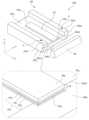
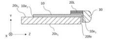
図1Aは、本開示の実施形態1におけるレーザ光源100の構成例を模式的に示す斜視図である。図1Bは、図1Aのレーザ光源100の平面構成を模式的に示す図である。本実施形態におけるレーザ光源100は、レーザダイオードチップ10と、レーザダイオードチップ10を支持するサブマウント20と、サブマウント20に支持されたコリメートレンズ30と、これらの素子または部品を収容する半導体レーザパッケージ40と、を備える。また、本実施形態におけるレーザ光源100は、半導体レーザパッケージ40を貫通し、レーザダイオードチップ10に電力を供給する一対のリード端子50を備える。半導体レーザパッケージ40は、蓋体40L、基体40b、および透光窓40wを含む。本実施形態におけるレーザ光源100において、レーザダイオードチップ10から出射され、コリメートレンズ30によってコリメートされたレーザ光が、透光窓40wから外部に取り出される。1A is a perspective view showing a schematic configuration example of alaser light source 100 inembodiment 1 of the present disclosure. FIG. 1B is a diagram showing a schematic planar configuration of thelaser light source 100 in FIG. 1A. Thelaser light source 100 in this embodiment includes alaser diode chip 10, asubmount 20 supporting thelaser diode chip 10, a collimatinglens 30 supported by thesubmount 20, and asemiconductor laser package 40 housing these elements or components. Thelaser light source 100 in this embodiment also includes a pair oflead terminals 50 that penetrate thesemiconductor laser package 40 and supply power to thelaser diode chip 10. Thesemiconductor laser package 40 includes alid 40L, abase 40b, and a light-transmittingwindow 40w. In thelaser light source 100 in this embodiment, the laser light emitted from thelaser diode chip 10 and collimated by the collimatinglens 30 is taken out from the light-transmittingwindow 40w.

図1Aでは、説明のわかりやすさのために半導体レーザパッケージ40における蓋体40L、基体40b、および透光窓40wが分離された状態で記載されているが、実際にはこれらは接合されている。図1Bでは、半導体レーザパッケージ40における蓋体40Lの記載が省略されている。In Fig. 1A, for ease of understanding, thelid 40L,base 40b, and light-transmittingwindow 40w in thesemiconductor laser package 40 are shown in a separated state, but in reality, they are joined together. In Fig. 1B, thelid 40L in thesemiconductor laser package 40 is omitted.

図面では、参考のために、互いに直交するX軸、Y軸およびZ軸が模式的に示されている。説明のわかりやすさのため、本開示では、基体40b内におけるレーザダイオードチップ10、サブマウント20、およびコリメートレンズ30が位置する側を「上」と表現する場合がある。このことは、レーザ光源100の使用時における向きを制限するわけではなく、レーザ光源100の向きは任意である。In the drawings, for reference, mutually orthogonal X-axis, Y-axis, and Z-axis are shown diagrammatically. For ease of explanation, in this disclosure, the side on which thelaser diode chip 10, thesubmount 20, and thecollimating lens 30 are located within thebase 40b may be referred to as "upper". This does not limit the orientation of thelaser light source 100 during use, and the orientation of thelaser light source 100 is arbitrary.

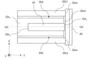
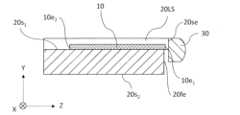
図2Aは、図1Aのレーザ光源100から半導体レーザパッケージ40および一対のリード端子50を省略した構成のより詳細を示す斜視図である。図2Aにおいて破線によって囲まれた領域は、サブマウント20に配置されたレーザダイオードチップ10の詳細な構造の例を表している。図2Aでは、サブマウント20およびコリメートレンズ30は分離された状態で記載されているが、実際にはこれらは接合されている。図2Bは、図2Aのレーザ光源100を模式的に示す上面図である。図2Cは、図2Bの構成のYZ平面に平行なIIC-IIC線断面図である。本開示では、サブマウント20を基準として、コリメートレンズ30が位置する側を「前方」と表現する場合がある。Figure 2A is a perspective view showing the details of the configuration of thelaser light source 100 of Figure 1A with thesemiconductor laser package 40 and the pair oflead terminals 50 omitted. The area surrounded by the dashed line in Figure 2A shows an example of the detailed structure of thelaser diode chip 10 arranged on thesubmount 20. In Figure 2A, thesubmount 20 and thecollimating lens 30 are shown in a separated state, but in reality they are joined together. Figure 2B is a top view showing a schematic diagram of thelaser light source 100 of Figure 2A. Figure 2C is a cross-sectional view of the configuration of Figure 2B along line IIC-IIC parallel to the YZ plane. In this disclosure, the side on which thecollimating lens 30 is located with respect to thesubmount 20 may be expressed as "front".

図2Aに示すように、レーザダイオードチップ10は、端面出射型のレーザダイオードチップであり、第1のクラッド層10C、第2のクラッド層10C、および発光層10Lを含む半導体積層構造体10aと、半導体積層構造体10aを支持する基板10bと、発光層10Lで発生した高出力のレーザ光を出射する出射端面10eと、出射端面10eとは反対側の後方端面10eとを有する。発光層10Lは、第1のクラッド層10Cと第2のクラッド層10Cとの間に位置する。レーザダイオードチップ10は、バッファ層およびコンタクト層などの他の層を含み得る。本開示では、「出射端面10e」を「第1の端面10e」と称し、「後方端面10e」を「第2の端面10e」と称することがある。 As shown in FIG. 2A, thelaser diode chip 10 is an edge-emitting type laser diode chip, and has a semiconductorlaminated structure 10a including a first cladding layer 10C1 , a second cladding layer 10C2 , and a light-emittinglayer 10L, asubstrate 10b supporting the semiconductor laminatedstructure 10a, anemission end face 10e1 for emitting high-power laser light generated in the light-emittinglayer 10L, and arear end face 10e2 opposite to theemission end face 10e1. The light-emittinglayer 10L is located between the first cladding layer 10C1 and the second cladding layer 10C2. Thelaser diode chip 10 may include other layers such as a buffer layer and a contact layer. In the present disclosure, the "emission end face 10e1 " may be referred to as the "first end face 10e1 ", and the "rear end face 10e2 " may be referred to as the "second end face 10e2 ".

レーザダイオードチップ10は、基板10bよりも発光層10Lがサブマウント20に近いフェイスダウンの状態で、サブマウント20に固定されている。レーザダイオードチップ10における半導体積層構造体10aおよび基板10bのY方向における合計のサイズは、80μm程度である。基板10bおよび第1のクラッド層10CのY方向における合計のサイズは、第2のクラッド層10CのY方向におけるサイズよりも大きい。フェイスダウンの状態では、基板10bよりも発光層10Lがサブマウント20から遠いフェイスアップの状態と比較して、発光層10Lとサブマウント20との距離が約10分の1である。したがって、フェイスダウンの状態では、発光層10Lから高出力のレーザ光が出射されても、発光層10Lで発生した熱を効率よくサブマウント20に伝えることができる。本実施形態におけるレーザ光の出力は、例えば3W以上50W以下である。 Thelaser diode chip 10 is fixed to thesubmount 20 in a face-down state in which thelight emitting layer 10L is closer to thesubmount 20 than thesubstrate 10b. The total size in the Y direction of the semiconductor laminatedstructure 10a and thesubstrate 10b in thelaser diode chip 10 is about 80 μm. The total size in the Y direction of thesubstrate 10b and the first cladding layer 10C1 is larger than the size in the Y direction of the second cladding layer 10C2. In the face-down state, the distance between the light emittinglayer 10L and thesubmount 20 is about one-tenth of that in the face-up state in which thelight emitting layer 10L is farther from thesubmount 20 than thesubstrate 10b. Therefore, in the face-down state, even if a high-power laser light is emitted from thelight emitting layer 10L, the heat generated in thelight emitting layer 10L can be efficiently transferred to thesubmount 20. The output of the laser light in this embodiment is, for example, 3 W or more and 50 W or less.

半導体積層構造体10aは、例えば量子井戸のエネルギー準位を形成するダブルヘテロ構造を有し得る。発光層10Lのバンドギャップは、第1のクラッド層10Cおよび第2のクラッド層10Cのバンドギャップよりも小さい。本実施形態において、基板10b、および基板10b上の第1のクラッド層10Cは、それぞれn型半導体から形成され得る。発光層10Lは、真性半導体、n型半導体、またはp型半導体から形成され、発光層10L上の第2のクラッド層10Cはp型半導体から形成され得る。n型およびp型は逆であってもよい。p型クラッド層からn型クラッド層への電流注入によって発光層10Lでキャリアの反転分布が生じ、発光層10Lから光が誘導放出される。発光層10Lの屈折率は第1のクラッド層10Cおよび第2のクラッド層10Cの屈折率よりも高く設計されており、発光層10Lで発生した光は、全反射によって発光層10L内に閉じ込められる。発光層10Lは共振器として機能し、発光層10Lの出射端面10eからレーザ光が出射される。発光層10Lの共振器長は、出射端面10eから後方端面10eまでの距離によって規定される。共振器長の方向はZ方向に対して平行である。共振器長は、例えば500μm以上5000μm以下である。共振器長が長い場合、レーザダイオードチップ10とサブマウント20との接触面積を広くすることができるので、発光層10Lで発生した熱を効率よくサブマウント20に伝えることができる。 The semiconductor laminatedstructure 10a may have, for example, a double heterostructure that forms an energy level of a quantum well. The band gap of thelight emitting layer 10L is smaller than the band gaps of the first cladding layer 10C1 and the second cladding layer 10C2. In this embodiment, thesubstrate 10b and the first cladding layer 10C1 on thesubstrate 10b may each be formed from an n-type semiconductor. Thelight emitting layer 10L may be formed from an intrinsic semiconductor, an n-type semiconductor, or a p-type semiconductor, and the second cladding layer 10C2 on thelight emitting layer 10L may be formed from a p-type semiconductor. The n-type and p-type may be reversed. Current injection from the p-type cladding layer to the n-type cladding layer causes carrier population inversion in thelight emitting layer 10L, and stimulated emission of light from thelight emitting layer 10L. The refractive index of thelight emitting layer 10L is designed to be higher than the refractive index of the first cladding layer 10C1 and the second cladding layer 10C2 , and the light generated in thelight emitting layer 10L is confined in thelight emitting layer 10L by total reflection. Thelight emitting layer 10L functions as a resonator, and laser light is emitted from theemission end face 10e1 of thelight emitting layer 10L. The resonator length of thelight emitting layer 10L is determined by the distance from theemission end face 10e1 to therear end face 10e2. The direction of the resonator length is parallel to the Z direction. The resonator length is, for example, 500 μm or more and 5000 μm or less. When the resonator length is long, the contact area between thelaser diode chip 10 and thesubmount 20 can be widened, so that the heat generated in thelight emitting layer 10L can be efficiently transferred to thesubmount 20.

レーザダイオードチップ10の出射端面10eから出射されたレーザ光は、伝搬するにつれてYZ平面において速く発散し、XZ平面において遅く発散する。レーザ光のスポットは、コリメートしない場合、ファーフィールドで、XY平面においてY方向が長軸でありX方向が短軸である楕円形状を有している。 The laser light emitted from the emission end surface10e1 of thelaser diode chip 10 diverges quickly in the YZ plane and diverges slowly in the XZ plane as it propagates. When not collimated, the spot of the laser light has an elliptical shape in the far field with the Y direction as the major axis and the X direction as the minor axis in the XY plane.

レーザダイオードチップ10は、可視領域における紫色、青色、緑色もしくは赤色のレーザ光、または赤外もしくは紫外のレーザ光を出射し得る。紫色の発光ピーク波長は、350nm以上419nm以下の範囲内にあることが望ましく、400nm以上415nm以下の範囲内にあることがより望ましい。青色光の発光ピーク波長は、420nm以上494nm以下の範囲内にあることが望ましく、440nm以上475nm以下の範囲内にあることがより望ましい。紫色または青色のレーザ光を出射する半導体レーザ素子としては、窒化物半導体を含む半導体レーザ素子が挙げられる。窒化物半導体としては、例えば、GaN、InGaN、およびAlGaNを用いることができる。緑色光の発光ピーク波長は、495nm以上570nm以下の範囲内にあることが望ましく、510nm以上550nm以下の範囲内にあることがより望ましい。緑色のレーザ光を出射する半導体レーザ素子としては、窒化物半導体を含む半導体レーザ素子が挙げられる。窒化物半導体としては、例えば、GaN、InGaN、およびAlGaNを用いることができる。赤色光の発光ピーク波長は、605nm以上750nm以下の範囲内にあることが望ましく、610nm以上700nm以下の範囲内にあることがより望ましい。赤色のレーザ光を出射する半導体レーザ素子としては、例えば、InAlGaP系、GaInP系、GaAs系およびAlGaAs系の半導体を含む半導体レーザ素子が挙げられる。赤色光の半導体レーザ素子として、2以上の導波路領域を備える半導体レーザ素子が用いられ得る。これらの半導体を含む半導体レーザ素子は、窒化物半導体を含む半導体レーザ素子と比べて、熱により出力が低下しやすい。導波路領域を増やすことによって熱を分散させて半導体レーザ素子の出力低下を低減することができる。Thelaser diode chip 10 can emit violet, blue, green or red laser light in the visible region, or infrared or ultraviolet laser light. The emission peak wavelength of the violet light is preferably in the range of 350 nm to 419 nm, more preferably in the range of 400 nm to 415 nm. The emission peak wavelength of the blue light is preferably in the range of 420 nm to 494 nm, more preferably in the range of 440 nm to 475 nm. Semiconductor laser elements that emit violet or blue laser light include semiconductor laser elements containing nitride semiconductors. Examples of nitride semiconductors that can be used include GaN, InGaN, and AlGaN. The emission peak wavelength of the green light is preferably in the range of 495 nm to 570 nm, more preferably in the range of 510 nm to 550 nm. Semiconductor laser elements that emit green laser light include semiconductor laser elements containing nitride semiconductors. As the nitride semiconductor, for example, GaN, InGaN, and AlGaN can be used. The emission peak wavelength of the red light is preferably in the range of 605 nm to 750 nm, and more preferably in the range of 610 nm to 700 nm. As the semiconductor laser element that emits the red laser light, for example, a semiconductor laser element including an InAlGaP-based, GaInP-based, GaAs-based, and AlGaAs-based semiconductor can be cited. As the semiconductor laser element of the red light, a semiconductor laser element having two or more waveguide regions can be used. The output of the semiconductor laser element including these semiconductors is more likely to decrease due to heat than that of the semiconductor laser element including the nitride semiconductor. By increasing the waveguide region, the heat can be dispersed, and the output decrease of the semiconductor laser element can be reduced.

サブマウント20は、レーザダイオードチップ10が固着された主平面20sと、レーザダイオードチップ10の出射端面10eの両側に位置する一対のレンズ支持部20LSと、主平面20sの反対側に位置する裏面20sと、主平面20sと裏面20sとをつなぐ前方端面20feとを有する。主平面20sおよび前方端面20feが主平面20sのエッジ20edを規定する。図2Aに示す例において、一対のレンズ支持部20LSは、レーザダイオードチップ10の両側に位置してZ方向に延びる一対の凸部である。サブマウント20は、前方端面20feよりも後ろでは、Z方向に延びる以下のU字型形状を有する。このU字型形状は、YZ平面に平行な平面に関して鏡面対称でありZ方向に延びる角筒体をXZ平面に平行な平面によって分割して形成される。一対のレンズ支持部20LSの端面20seは、レーザダイオードチップ10の出射端面10eよりも共振器長方向に突出している。主平面20sの法線方向は、Y方向に対して平行である。 Thesubmount 20 has amain plane 20s1 to which thelaser diode chip 10 is fixed, a pair of lens support parts 20LS located on both sides of theemission end surface 10e1 of thelaser diode chip 10, aback surface 20s2 located on the opposite side of themain plane 20s1 , and a front end surface 20fe connecting themain plane 20s1 and theback surface 20s2. Themain plane 20s1 and the front end surface 20fe define an edge 20ed of themain plane 20s1. In the example shown in FIG. 2A, the pair of lens support parts 20LS are a pair of convex parts located on both sides of thelaser diode chip 10 and extending in the Z direction. Thesubmount 20 has the following U-shaped shape extending in the Z direction behind the front end surface 20fe. This U-shaped shape is formed by dividing a square cylinder that is mirror symmetric with respect to a plane parallel to the YZ plane and extends in the Z direction by a plane parallel to the XZ plane. End faces 20se of the pair of lens support parts 20LS protrude in the cavity length direction beyond the emission end face10e1 of thelaser diode chip 10. The normal direction of the main plane20s1 is parallel to the Y direction.

一対のレンズ支持部20LSの端面20seと、レーザダイオードチップ10の出射端面10eとのZ方向における距離は、コリメートレンズ30の焦点距離にほぼ等しくなるように設計され得る。一対のレンズ支持部20LSの端面20seと、レーザダイオードチップ10の出射端面10eとのZ方向における距離は、例えば50μm以上100μm以下である。一対のレンズ支持部20LSのY方向におけるサイズは、コリメートレンズ30のY方向におけるサイズと同程度であり得る。一対のレンズ支持部20LSのY方向におけるサイズは、コリメートレンズ30のY方向におけるサイズよりも大きくてもよいし、等しくてもよいし、小さくてもよい。一対のレンズ支持部20LSのY方向におけるサイズは、例えば100μm以上500μm以下である。 The distance in the Z direction between the end faces 20se of the pair of lens support parts 20LS and theemission end face 10e1 of thelaser diode chip 10 can be designed to be approximately equal to the focal length of thecollimator lens 30. The distance in the Z direction between the end faces 20se of the pair of lens support parts 20LS and theemission end face 10e1 of thelaser diode chip 10 is, for example, 50 μm or more and 100 μm or less. The size in the Y direction of the pair of lens support parts 20LS can be approximately the same as the size in the Y direction of thecollimator lens 30. The size in the Y direction of the pair of lens support parts 20LS may be larger than, equal to, or smaller than the size in the Y direction of thecollimator lens 30. The size in the Y direction of the pair of lens support parts 20LS is, for example, 100 μm or more and 500 μm or less.

サブマウント20のX方向におけるサイズは、例えば1mm以上3mm以下であり、サブマウント20のうち、一対のレンズ支持部20LS以外の部分のY方向におけるサイズは、例えば100μm以上500μm以下であり、一対のレンズ支持部20LS以外の部分のZ方向におけるサイズは、例えば1mm以上6mm以下である。本開示において、サイズの上限は、レーザ光源100の小型化の観点から決定され得る。The size of thesubmount 20 in the X direction is, for example, 1 mm or more and 3 mm or less, the size of the portion of thesubmount 20 other than the pair of lens support portions 20LS in the Y direction is, for example, 100 μm or more and 500 μm or less, and the size of the portion of thesubmount 20 other than the pair of lens support portions 20LS in the Z direction is, for example, 1 mm or more and 6 mm or less. In the present disclosure, the upper limit of the size may be determined from the viewpoint of miniaturization of thelaser light source 100.

サブマウント20において、レーザダイオードチップ10の出射端面10eは、主平面20sのエッジ20edよりも共振器長方向に突出している。レーザダイオードチップ10の出射端面10eと、主平面20sのエッジ20edとのZ方向における距離は、例えば2μm以上50μm以下である。この配置により、フェイスダウンの状態で、レーザダイオードチップ10とサブマウント20の主平面20sとが、例えば金すずなどの無機材料の接合材で固着されても、接合材が発光層10Lの出射端面10eにせり上がることを抑制することができる。特許文献1に開示されているレーザ光源では、レーザダイオードチップがフェイスダウンの状態で配置される場合、レーザダイオードチップとサブマウントとを接合する接合材が、レーザダイオードチップにおける発光層の出射端面にせり上がる可能性がある。その結果、レーザダイオードチップから出射されるレーザ光の出力が低下し得る。本実施形態におけるレーザ光源100では、このようなレーザ光の出力の低下を抑制することができる。 In thesubmount 20, theemission end surface 10e1 of thelaser diode chip 10 protrudes in the cavity length direction beyond the edge 20ed of themain plane 20s1. The distance in the Z direction between theemission end surface 10e1 of thelaser diode chip 10 and the edge 20ed of themain plane 20s1 is, for example, 2 μm or more and 50 μm or less. With this arrangement, even if thelaser diode chip 10 and themain plane 20s1 of thesubmount 20 are fixed with an inorganic bonding material such as gold-tin in a face-down state, the bonding material can be prevented from rising up to theemission end surface 10e1 of the light-emittinglayer 10L. In the laser light source disclosed inPatent Document 1, when the laser diode chip is placed in a face-down state, the bonding material bonding the laser diode chip and the submount may rise up to the emission end surface of the light-emitting layer in the laser diode chip. As a result, the output of the laser light emitted from the laser diode chip may decrease. In thelaser light source 100 of this embodiment, such a decrease in the output of the laser light can be suppressed.

サブマウント20の一部または全体は、例えば、AlN、SiC、およびアルミナからなる群から選択される少なくとも1つを含むセラミックおよびCuWなどの合金から形成され得る。サブマウント20は、例えばセラミックの粉末を焼結することによって作製することができる。セラミックの熱伝導率は、例えば、10[W/m・K]以上500[W/m・K]以下であり得る。また、レーザダイオードチップ10の固着時に加えられる熱による変形を抑制するために、セラミックは低い熱膨張率を有し得る。熱膨張率は、2×10-6[1/K]以上1×10-5[1/K]以下であり得る。サブマウント20における主平面20sおよび裏面20sには、厚さが例えば0.5μm以上10μm以下である金めっきなどの金属膜が形成されていてもよい。主平面20sに形成された金属膜により、レーザダイオードチップ10を主平面20sに例えば金すずで接合することができる。裏面20sに形成された金属膜により、サブマウント20を底部40bに例えば金すずで接合することができる。 A part or the whole of thesubmount 20 may be formed of, for example, a ceramic containing at least one selected from the group consisting of AlN, SiC, and alumina, and an alloy such as CuW. Thesubmount 20 may be produced, for example, by sintering ceramic powder. The thermal conductivity of the ceramic may be, for example, 10 [W/m·K] or more and 500 [W/m·K] or less. In addition, the ceramic may have a low thermal expansion coefficient in order to suppress deformation due to heat applied when thelaser diode chip 10 is fixed. The thermal expansion coefficient may be 2×10⁻⁶ [1/K] or more and 1×10⁻⁵ [1/K] or less. A metal film such as gold plating having a thickness of, for example, 0.5 μm or more and 10 μm or less may be formed on themain plane 20s1 and theback surface 20s2 of thesubmount 20. The metal film formed on themain plane 20s1 allows thelaser diode chip 10 to be bonded to themain plane 20s1 with, for example, gold tin. The metal film formed on the back surface20s2 allows thesubmount 20 to be bonded to the bottom portion40b1 with, for example, gold-tin.

コリメートレンズ30は、レーザダイオードチップ10から出射されたレーザ光のうち、YZ平面において大きく発散する成分をコリメートする、いわゆるFAC(Fast Axis Collimator)レンズである。レーザ光のうち、XZ平面において小さく発散する成分をコリメートする、不図示のいわゆるSAC(Slow Axis Collimator)レンズは必要に応じてレーザ光源100の外部に配置され得る。本開示において、「コリメートする」とは、レーザ光を平行光にすることだけではなく、レーザ光の発散角を低減することも含む。なお、用途によっては、コリメートレンズ30の代わりに、集光レンズなどの他のレンズを用いてもよい。The collimatinglens 30 is a so-called FAC (Fast Axis Collimator) lens that collimates the components of the laser light emitted from thelaser diode chip 10 that diverge greatly in the YZ plane. A so-called SAC (Slow Axis Collimator) lens (not shown) that collimates the components of the laser light that diverge little in the XZ plane can be arranged outside thelaser light source 100 as necessary. In this disclosure, "collimating" includes not only making the laser light parallel, but also reducing the divergence angle of the laser light. Note that, depending on the application, other lenses such as a condenser lens may be used instead of the collimatinglens 30.

コリメートレンズ30は、X方向に延びる構造を有するシリンドリカルレンズであり、X軸方向には曲率を持たず、Y方向に曲率を持っている。コリメートレンズ30が延びる方向は、サブマウント20の主平面20sの法線方向、および共振器長方向の両方に垂直な方向である。コリメートレンズ30および一対のレンズ支持部20LSのY方向におけるサイズは同程度であるので、コリメートレンズ30の重心が、共振器長方向から見たとき、一対のレンズ支持部20LSの間に位置するように設けることが容易である。コリメートレンズ30の重心のこの配置関係により、コリメートレンズ30を安定的に精度よくサブマウント20に設けることができる。 Thecollimator lens 30 is a cylindrical lens having a structure extending in the X direction, has no curvature in the X-axis direction, and has a curvature in the Y direction. The direction in which thecollimator lens 30 extends is perpendicular to both the normal direction of the main plane20s1 of thesubmount 20 and the cavity length direction. Since the sizes of thecollimator lens 30 and the pair of lens support parts 20LS in the Y direction are approximately the same, it is easy to provide thecollimator lens 30 so that its center of gravity is located between the pair of lens support parts 20LS when viewed from the cavity length direction. This arrangement of the center of gravity of thecollimator lens 30 allows thecollimator lens 30 to be stably and accurately provided on thesubmount 20.

本実施形態では、サブマウント20における裏面20sを基準とした場合、一対のレンズ支持部20LSの上面のY方向における高さは、コリメートレンズ30の上面のY方向における高さにほぼ等しい。一対のレンズ支持部20LSに対するコリメートレンズ30の位置は、上記の2つの高さがほぼ等しくなるように粗調整される。その後、レーザダイオードチップ10からレーザ光を出射させながら、当該レーザ光が適切にコリメートされるように、一対のレンズ支持部20LSに対するコリメートレンズ30の位置が微調整される。なお、上記の2つの高さは必ずしもほぼ等しい必要はなく、異なっていてもよい。 In this embodiment, when the rear surface20s2 of thesubmount 20 is used as a reference, the height of the upper surface of the pair of lens support parts 20LS in the Y direction is approximately equal to the height of the upper surface of thecollimator lens 30 in the Y direction. The position of thecollimator lens 30 relative to the pair of lens support parts 20LS is roughly adjusted so that the above two heights are approximately equal. Thereafter, while emitting laser light from thelaser diode chip 10, the position of thecollimator lens 30 relative to the pair of lens support parts 20LS is finely adjusted so that the laser light is appropriately collimated. Note that the above two heights do not necessarily need to be approximately equal and may be different.

本実施形態におけるコリメートレンズ30はX方向に沿って一様であるので、レーザダイオードチップ10の出射端面10eと、コリメートレンズ30とのX方向における位置合わせを考慮する必要はない。コリメートレンズ30のうち、レーザダイオードチップ10の出射端面10eに対向する対向部分およびその周辺部分だけがX方向に沿って一様であればよい。したがって、それ以外の両側部分は、必ずしもX方向に沿って一様である必要はなく、透明である必要もない。コリメートレンズ30の両側部分のY方向におけるサイズは、対向部分およびその周辺部分のY方向におけるサイズよりも大きくてもよいし、等しくてもよいし、小さくてもよい。コリメートレンズ30は、例えば、ガラス、石英、合成石英、サファイア、透明セラミック、およびプラスチックの少なくとも1つから形成され得る。 Since the collimatinglens 30 in this embodiment is uniform along the X direction, there is no need to consider the alignment of theemission end surface 10e1 of thelaser diode chip 10 with the collimatinglens 30 in the X direction. Of the collimatinglens 30, only the facing portion facing theemission end surface 10e1 of thelaser diode chip 10 and its peripheral portion need to be uniform along the X direction. Therefore, the other two side portions do not necessarily need to be uniform along the X direction, and do not necessarily need to be transparent. The size of the two side portions of the collimatinglens 30 in the Y direction may be larger, equal, or smaller than the size of the facing portion and its peripheral portion in the Y direction. The collimatinglens 30 may be formed of at least one of, for example, glass, quartz, synthetic quartz, sapphire, transparent ceramic, and plastic.

コリメートレンズ30は、一対のレンズ支持部20LSの端面20seに、Z方向に接合されている。コリメートレンズ30と一対のレンズ支持部20LSの端面20seとを接合する接合材の厚さに多少のばらつきがあっても、そのばらつきはコリメートレンズ30のY方向における位置にはほとんど影響を及ぼさない。本実施形態の構成とは異なり、主平面20sに平行な平面を有する台座をサブマウント20の前に配置し、その台座の平面上にコリメートレンズ30を設けることも可能である。しかし、そのような構成では、コリメートレンズ30と台座の平面との間の接合材の厚さにばらつきが生じると、レーザダイオードチップ10とコリメートレンズ30とのY方向における位置ずれが生じ、レーザ光源100から外部に出射されたレーザ光の光軸の向きが大きくずれる可能性がある。これに対し、本実施形態では、レーザダイオードチップ10とコリメートレンズ30とのY方向における位置ずれが生じにくくなり、レーザ光源100から外部に出射されたレーザ光の光軸を設計通りの方向に向けることができる。接合材の厚さに多少のばらつきが発生しても、コリメートレンズ30の位置はレーザ光の光軸に沿って多少変化するだけなので、そのばらつきはレーザ光の光軸の向きにほとんど影響を及ぼさない。 Thecollimator lens 30 is bonded to the end faces 20se of the pair of lens support parts 20LS in the Z direction. Even if there is some variation in the thickness of the bonding material bonding thecollimator lens 30 to the end faces 20se of the pair of lens support parts 20LS, the variation has almost no effect on the position of thecollimator lens 30 in the Y direction. Unlike the configuration of this embodiment, it is also possible to place a pedestal having a flat surface parallel to the main flat surface20s1 in front of thesubmount 20 and provide thecollimator lens 30 on the flat surface of the pedestal. However, in such a configuration, if there is variation in the thickness of the bonding material between thecollimator lens 30 and the flat surface of the pedestal, a positional deviation in the Y direction between thelaser diode chip 10 and thecollimator lens 30 occurs, and the direction of the optical axis of the laser light emitted to the outside from thelaser light source 100 may be significantly shifted. In contrast, in this embodiment, positional deviation in the Y direction between thelaser diode chip 10 and thecollimator lens 30 is less likely to occur, and the optical axis of the laser light emitted to the outside from thelaser light source 100 can be directed in the direction as designed. Even if some variation occurs in the thickness of the bonding material, the position of thecollimator lens 30 only changes slightly along the optical axis of the laser light, and the variation has almost no effect on the direction of the optical axis of the laser light.

コリメートレンズ30と、一対のレンズ支持部20LSの端面20seとは、例えば金すずなどの無機材料の接合材で接合され得る。コリメートレンズ30の接合面、および一対のレンズ支持部20LSの端面20seには、前もって金属膜が形成されていてもよい。これらの金属膜により、例えば金すずでの接合が可能になる。金すずの接合温度は、約280℃である。サブマウント20を形成するセラミックの熱伝導率が低ければ、コリメートレンズ30と、一対のレンズ支持部20LSの端面20seとの接合時の熱がレーザダイオードチップ10に与える影響を低減することができる。The collimatinglens 30 and the end faces 20se of the pair of lens support parts 20LS can be bonded with an inorganic bonding material such as gold-tin. Metal films may be formed in advance on the bonding surfaces of the collimatinglens 30 and the end faces 20se of the pair of lens support parts 20LS. These metal films enable bonding with, for example, gold-tin. The bonding temperature of gold-tin is about 280°C. If the thermal conductivity of the ceramic forming thesubmount 20 is low, the effect of heat on thelaser diode chip 10 during bonding between the collimatinglens 30 and the end faces 20se of the pair of lens support parts 20LS can be reduced.

他の例として、コリメートレンズ30と、一対のレンズ支持部20LSの端面20seとは、熱硬化樹脂を含む接合材で接合され得る。熱硬化樹脂の接合温度は約100℃であり、無機材料の接合温度よりも低い。したがって、コリメートレンズ30と、一対のレンズ支持部20LSの端面20seとの接合時の熱がレーザダイオードチップ10に与える影響をさらに低減することができる。コリメートレンズ30と、一対のレンズ支持部20LSの端面20seとの接合では、熱硬化樹脂は、例えば、図2Aに示す点Pの位置をレーザ光で照射することによって加熱され得る。点Pの位置と、一対のレンズ支持部20LSの端面20seとのZ方における距離は、例えば50μm以上500μm以下である。本実施形態では、上面視で、レーザダイオードチップ10から出射されたレーザ光の光軸と、接合材とが重ならないので、熱硬化樹脂を含む接合材からアウトガスが発生したとしても、アウトガスがレーザダイオードチップ10に近づくことを抑制することができる。その結果、レーザダイオードチップ10の出射端面10eにおいて後述する集塵が生じることを抑制することができる。 As another example, thecollimator lens 30 and the end faces 20se of the pair of lens support parts 20LS may be bonded with a bonding material containing a thermosetting resin. The bonding temperature of the thermosetting resin is about 100° C., which is lower than the bonding temperature of the inorganic material. Therefore, the influence of heat on thelaser diode chip 10 during bonding between thecollimator lens 30 and the end faces 20se of the pair of lens support parts 20LS can be further reduced. In bonding between thecollimator lens 30 and the end faces 20se of the pair of lens support parts 20LS, the thermosetting resin may be heated, for example, by irradiating the position of point P shown in FIG. 2A with laser light. The distance in the Z direction between the position of point P and the end faces 20se of the pair of lens support parts 20LS is, for example, 50 μm or more and 500 μm or less. In this embodiment, the optical axis of the laser light emitted from thelaser diode chip 10 does not overlap with the bonding material when viewed from above, so that even if outgas is generated from the bonding material containing the thermosetting resin, the outgas can be suppressed from approaching thelaser diode chip 10. As a result, dust collection at the light-emittingend surface 10e-1 of thelaser diode chip 10 can be suppressed, as will be described later.

一部の無機材料の接合材は、バインダとして有機物を含み得る。コリメートレンズ30と一対のレンズ支持部20LSの端面20seとの接合に当該接合材を用いても、加熱によって発生するアウトガスがレーザダイオードチップ10に近づくことを抑制することができる。Some inorganic bonding materials may contain organic matter as a binder. Even if such a bonding material is used to bond the collimatinglens 30 to the end faces 20se of the pair of lens support parts 20LS, outgassing generated by heating can be prevented from approaching thelaser diode chip 10.

コリメートレンズ30と一対のレンズ支持部20LSの端面20seとを、接合材を用いずに、直接接合(direct bonding)によって接合してもよい。直接接合の例は、拡散接合、常温接合、および陽極接合を含む。The collimatinglens 30 and the end faces 20se of the pair of lens support parts 20LS may be bonded by direct bonding without using a bonding material. Examples of direct bonding include diffusion bonding, room temperature bonding, and anodic bonding.

接合材を用いる実施形態の説明から明らかなように、直接接合による接合でも、接合材を用いた接合と同様に、コリメートレンズ30のY方向における位置ずれを抑制することができる。As is clear from the description of the embodiment using a bonding material, even with direct bonding, the positional deviation of thecollimator lens 30 in the Y direction can be suppressed, just like with bonding using a bonding material.

本実施形態におけるレーザ光源100では、サブマウント20が、レーザダイオードチップ10およびコリメートレンズ30を支持している。レーザダイオードチップ10の出射端面10eとコリメートレンズ30との距離が短いことから、レーザダイオードチップ10から出射されたレーザ光が大きく発散する前に、小さいコリメートレンズ30によってその発散を低減することができる。したがって、小型のレーザ光源100を実現することが可能になる。また、コリメートレンズ30を通過したコリメートビームの直径を小さくすることが可能になる。 In thelaser light source 100 of this embodiment, thesubmount 20 supports thelaser diode chip 10 and thecollimator lens 30. Since the distance between the emission end surface10e1 of thelaser diode chip 10 and thecollimator lens 30 is short, thesmall collimator lens 30 can reduce the divergence of the laser light emitted from thelaser diode chip 10 before it diverges significantly. Therefore, it is possible to realize a small-sizedlaser light source 100. In addition, it is possible to reduce the diameter of the collimated beam that has passed through thecollimator lens 30.

半導体レーザパッケージ40は、レーザダイオードチップ10、サブマウント20、およびコリメートレンズ30を気密に封止してもよい。レーザダイオードチップ10が、例えば350nm以上570nm以下の短波長のレーザ光を出射する場合、雰囲気に含まれる有機ガス成分などがレーザ光によって分解され、分解物がレーザダイオードチップ10の出射端面10eに付着することがある。また、レーザダイオードチップ10の出射端面10eが外気に接していると、集塵などにより、動作中に端面劣化が進行していく可能性もある。このような端面劣化は、レーザダイオードチップ10の光出力の低下を招き得る。レーザダイオードチップ10の信頼性を高めて寿命を延ばすため、半導体レーザパッケージ40は、レーザダイオードチップ10を気密に封止していることが望ましい。半導体レーザパッケージ40による気密封止は、レーザダイオードチップ10から出射されるレーザ光の波長の長短にかかわらず行われてもよい。 Thesemiconductor laser package 40 may hermetically seal thelaser diode chip 10, thesubmount 20, and thecollimating lens 30. When thelaser diode chip 10 emits a short wavelength laser light, for example, 350 nm or more and 570 nm or less, organic gas components contained in the atmosphere may be decomposed by the laser light, and the decomposed products may adhere to theemission end face 10e1 of thelaser diode chip 10. In addition, if theemission end face 10e1 of thelaser diode chip 10 is in contact with the outside air, the end face may deteriorate during operation due to dust collection, etc. Such end face deterioration may lead to a decrease in the optical output of thelaser diode chip 10. In order to increase the reliability of thelaser diode chip 10 and extend its life, it is desirable that thesemiconductor laser package 40 hermetically seals thelaser diode chip 10. The hermetic sealing by thesemiconductor laser package 40 may be performed regardless of the length of the wavelength of the laser light emitted from thelaser diode chip 10.

半導体レーザパッケージ40における基体40bは、サブマウント20の裏面20sに熱的に接触する。基体40bは、熱伝導率の高い材料から形成され得る。当該材料は、例えば、Cu、Al、Ag、Fe、Ni、Mo、Cu、W、およびCuMoからなる群から選択される少なくとも1つを含む金属である。レーザダイオードチップ10の出射端面10eと透光窓40wとの高さを合わせるために、基体40bにおける底面40btと、サブマウント20との間に、図1Bに示すように、熱伝導率が高い部材40mが設けられていてもよい。部材40mは、基体40bの底面40btを含む部分と同じ材料から形成され得る。あるいは、基体40bにおける底面40btの少なくとも一部が盛り上がっており、その盛り上がった底面40bt上にサブマウント20を配置してもよい。基体40bにおける底面40btを含む部分は、例えば銅から形成され得る。基体40bにおけるレーザダイオード10、サブマウント20およびコリメートレンズ30を囲む部分は、例えばコバールから形成され得る。コバール(kovar)は、主成分である鉄にニッケルおよびコバルトを加えた合金である。半導体レーザパッケージ40における蓋体40Lは、基体40bと同じ材料から形成されてもよいし、異なる材料から形成されてもよい。半導体レーザパッケージ40における透光窓40wは、基体40bに取り付けられ、レーザダイオードチップ10から出射されたレーザ光を透過させる。半導体レーザパッケージ40における透光窓40wは、コリメートレンズ30と同様に、例えば、ガラス、石英、合成石英、サファイア、透明セラミック、およびプラスチックの少なくとも1つから形成され得る。 Thebase 40b in thesemiconductor laser package 40 is in thermal contact with the back surface20s2 of thesubmount 20. Thebase 40b may be made of a material with high thermal conductivity. The material may be, for example, a metal containing at least one selected from the group consisting of Cu, Al, Ag, Fe, Ni, Mo, Cu, W, and CuMo. In order to match the height of the emission end surface10e1 of thelaser diode chip 10 and the light-transmittingwindow 40w, amember 40m with high thermal conductivity may be provided between the bottom surface 40bt of thebase 40b and thesubmount 20, as shown in FIG. 1B. Themember 40m may be made of the same material as the portion including the bottom surface 40bt of thebase 40b. Alternatively, at least a part of the bottom surface 40bt of thebase 40b may be raised, and thesubmount 20 may be disposed on the raised bottom surface 40bt. The portion of the base 40b including the bottom surface 40bt may be made of, for example, copper. The portion of thebase 40b surrounding thelaser diode 10, thesubmount 20, and thecollimating lens 30 may be made of, for example, kovar. Kovar is an alloy in which nickel and cobalt are added to iron, which is the main component. Thecover 40L in thesemiconductor laser package 40 may be made of the same material as thebase 40b, or may be made of a different material. The light-transmittingwindow 40w in thesemiconductor laser package 40 is attached to thebase 40b and transmits the laser light emitted from thelaser diode chip 10. The light-transmittingwindow 40w in thesemiconductor laser package 40 may be made of at least one of glass, quartz, synthetic quartz, sapphire, transparent ceramic, and plastic, similar to thecollimating lens 30.

一対のリード端子50は、それぞれ、レーザダイオードチップ10に、ワイヤによって以下のように電気的に接続されている。図2Aに示す例において、レーザダイオードチップ10の上面には金メッキなどの金属膜が形成される。当該金属膜と一対のリード端子50の一方とがワイヤによって電気的に接続される。同様に、サブマウント20の主平面20sにも金メッキなどの金属膜が形成される。当該金属膜と一対のリード端子50の他方とがワイヤによって電気的に接続される。一対のリード端子50によってレーザダイオードチップ10における第2のクラッド層10Cから第1のクラッド層10Cに電流が注入される。一対のリード端子50は、レーザダイオードチップ10から出射されるレーザ光の出射タイミングおよび出力を調整する不図示の外部回路に電気的に接続されている。一対のリード端子50は、導通性のよい材料から形成されている。当該材料として、例えばFe-Ni合金、またはCu合金などの金属が挙げられる。 The pair oflead terminals 50 are electrically connected to thelaser diode chip 10 by wires as follows. In the example shown in FIG. 2A, a metal film such as gold plating is formed on the upper surface of thelaser diode chip 10. The metal film and one of the pair oflead terminals 50 are electrically connected by wires. Similarly, a metal film such as gold plating is also formed on themain plane 20s1 of thesubmount 20. The metal film and the other of the pair oflead terminals 50 are electrically connected by wires. A current is injected from the second cladding layer 10C2 to the first cladding layer 10C1 in thelaser diode chip 10 by the pair oflead terminals 50. The pair oflead terminals 50 are electrically connected to an external circuit (not shown) that adjusts the emission timing and output of the laser light emitted from thelaser diode chip 10. The pair oflead terminals 50 are formed of a material with good conductivity. Examples of the material include metals such as Fe-Ni alloys and Cu alloys.

本実施形態におけるレーザ光源100では、サブマウント20が、一対のレンズ支持部20LSの間の主平面20sによってレーザダイオードチップ10を支持し、一対のレンズ支持部20LSの端面20seによってコリメートレンズ30を支持している。これにより、前述したように、レーザダイオードチップ10とコリメートレンズ30との位置合わせが容易になり、小型のレーザ光源100を実現することが可能になる。さらに、本実施形態におけるレーザ光源100では、レーザダイオードチップ10がサブマウント20にフェイスダウンの状態で配置されても、接合材がレーザダイオードチップ10の出射端面10eにせり上がることを抑制することができる。 In thelaser light source 100 of this embodiment, thesubmount 20 supports thelaser diode chip 10 by the main plane20s1 between the pair of lens support parts 20LS, and supports thecollimator lens 30 by the end face 20se of the pair of lens support parts 20LS. This makes it easy to align thelaser diode chip 10 and thecollimator lens 30 as described above, and makes it possible to realize a compactlaser light source 100. Furthermore, in thelaser light source 100 of this embodiment, even if thelaser diode chip 10 is placed face-down on thesubmount 20, it is possible to prevent the bonding material from rising up to the emission end face10e1 of thelaser diode chip 10.

(実施形態1の変形例)
次に、本開示の実施形態1におけるレーザ光源100の変形例1から変形例5を説明する。以下の変形例では、半導体レーザパッケージ40、および一対のリード端子50の記載が省略されている。前述と重複する説明は省略することがある。
(Modification of the first embodiment)
Next, modified examples 1 to 5 of thelaser light source 100 according to the first embodiment of the present disclosure will be described. In the following modified examples, thesemiconductor laser package 40 and the pair oflead terminals 50 are omitted. Descriptions that overlap with those described above may be omitted.

図3Aから図3Cを参照して、本開示の実施形態1の変形例1におけるレーザ光源110の構成例を説明する。図3Aは、本開示の実施形態1の変形例1におけるレーザ光源110の構成例を模式的に示す斜視図である。図3Bは、図3Aのレーザ光源110を模式的に示す上面図である。図3Cは、図3Bの構成のYZ平面に平行なIIIC-IIIC線断面図である。実施形態1の変形例1におけるレーザ光源110が実施形態1におけるレーザ光源100と異なる点は、サブマウント20の形状である。サブマウント20における前方端面20feは、中央端面20fe、および中央端面20feの両側に位置する両側端面20feを有する。中央端面20feは、両側端面20feよりも共振器長方向に窪んでいる。実施形態1の変形例1における主平面20sのエッジ20edは、主平面20sと中央端面20feとによって規定されている。中央端面20feの窪みのZ方向におけるサイズは、例えば5μm以上100μm以下であり、X方向におけるサイズは、例えば50μm以上200μm以下であり、Y向における主平面20sからのサイズは、例えば100μm以上500μm以下である。窪みは、必ずしもY方向に貫通する必要はない。 A configuration example of thelaser light source 110 inModification 1 of theembodiment 1 of the present disclosure will be described with reference to Figures 3A to 3C. Figure 3A is a perspective view that shows a schematic configuration example of thelaser light source 110 inModification 1 of theembodiment 1 of the present disclosure. Figure 3B is a top view that shows a schematic configuration example of thelaser light source 110 in Figure 3A. Figure 3C is a cross-sectional view of the configuration of Figure 3B along line IIIC-IIIC parallel to the YZ plane. Thelaser light source 110 inModification 1 of theembodiment 1 differs from thelaser light source 100 in theembodiment 1 in the shape of thesubmount 20. The front end surface 20fe in thesubmount 20 has a central end surface 20fe1 and both side end surfaces 20fe2 located on both sides of the central end surface 20fe1. The central end surface 20fe1 is recessed in the cavity length direction from both side end surfaces 20fe2 . The edge 20ed of the main plane20s1 in the first modified example of the first embodiment is defined by the main plane20s1 and the central end face20fe1 . The size of the recess in the central end face20fe1 in the Z direction is, for example, 5 μm to 100 μm, the size in the X direction is, for example, 50 μm to 200 μm, and the size from the main plane20s1 in the Y direction is, for example, 100 μm to 500 μm. The recess does not necessarily need to penetrate in the Y direction.

レーザダイオードチップ10の出射端面10eは、主平面20sと中央端面20feとによって規定される主平面20sのエッジ20edよりも共振器長方向に突出している。サブマウント20における両側端面20feは、一対のレンズ支持部20LSの端面20seと同様に、レーザダイオードチップ10の出射端面10eよりも共振器長方向に突出している。主平面20sと中央端面20feとによって規定される主平面20sのエッジ20edにより、接合材がレーザダイオードチップ10の出射端面10eにせり上がることを抑制することができる。実施形態1の変形例1におけるサブマウント20は、Z方向に延びる前述したU字型形状において前方端面20feの一部だけを除去すればよいので作製が容易であり得る。また、コリメートレンズ30は、一対のレンズ支持部20LSの端面20seおよび両側端面20feを含むL字型の端面に接合されるため、コリメートレンズ30とサブマウント20との接触面積が広くなり、接合が容易になり得る。 Theemission end face 10e1 of thelaser diode chip 10 protrudes in the cavity length direction beyond the edge 20ed of themain plane 20s1 defined by themain plane 20s1 and the central end face 20fe1. The two end faces 20fe2 of thesubmount 20 protrude in the cavity length direction beyond theemission end face 10e1 of thelaser diode chip 10, similar to the end faces 20se of the pair of lens supports 20LS. The edge 20ed of themain plane 20s1 defined by themain plane 20s1 and the central end face 20fe1 can prevent the bonding material from rising up to theemission end face 10e1 of thelaser diode chip 10. Thesubmount 20 in the first modification of the first embodiment can be easily manufactured because it is only necessary to remove a part of the front end face 20fe in the above-mentioned U-shaped shape extending in the Z direction. In addition, since thecollimator lens 30 is bonded to the L-shaped end face including the end face 20se and both side end faces20fe2 of the pair of lens support parts 20LS, the contact area between thecollimator lens 30 and thesubmount 20 is increased, making bonding easier.

次に、図4Aから図4Cを参照して、本開示の実施形態1の変形例2におけるレーザ光源120の構成例を説明する。図4Aは、本開示の実施形態1の変形例2におけるレーザ光源120の構成例を模式的に示す斜視図である。図4Bは、図4Aのレーザ光源120を模式的に示す上面図である。図4Cは、図4Bの構成のYZ平面に平行なIVC-IVC線断面図である。実施形態1の変形例2におけるレーザ光源120が実施形態1におけるレーザ光源100と異なる点は、サブマウント20の形状である。実施形態1の変形例2におけるサブマウント20は、一対のレンズ支持部20LSのそれぞれとレーザダイオードチップ10との間に、共振器長方向に沿って延びる溝20dを有している。図4Bに示す例では、溝20dは、一対のレンズ支持部20LSに隣接しているが、必ずしも隣接する必要はない。溝20dのX方向におけるサイズは、例えば100μm以上500μm以下であり、Y方向におけるサイズは、例えば50μm以上300μm以下であり、Z方向における主平面20sのエッジ20edからのサイズは、例えば1mm以上6mm以下である。溝20dは、必ずしもZ方向に貫通する必要はない。溝20dにより、コリメートレンズ30と一対のレンズ支持部20LSの端面20seとの接合時における熱がレーザダイオードチップ10に与える影響を低減することができる。 Next, with reference to FIG. 4A to FIG. 4C, a configuration example of thelaser light source 120 in the modified example 2 of theembodiment 1 of the present disclosure will be described. FIG. 4A is a perspective view that shows a schematic configuration example of thelaser light source 120 in the modified example 2 of theembodiment 1 of the present disclosure. FIG. 4B is a top view that shows a schematic configuration example of thelaser light source 120 in FIG. 4A. FIG. 4C is a cross-sectional view of the IVC-IVC line parallel to the YZ plane of the configuration of FIG. 4B. Thelaser light source 120 in the modified example 2 of theembodiment 1 differs from thelaser light source 100 in theembodiment 1 in the shape of thesubmount 20. Thesubmount 20 in the modified example 2 of theembodiment 1 has agroove 20d that extends along the resonator length direction between each of the pair of lens supports 20LS and thelaser diode chip 10. In the example shown in FIG. 4B, thegroove 20d is adjacent to the pair of lens supports 20LS, but does not necessarily have to be adjacent. The size of thegroove 20d in the X direction is, for example, 100 μm to 500 μm, the size in the Y direction is, for example, 50 μm to 300 μm, and the size in the Z direction from the edge 20ed of the main plane20s1 is, for example, 1 mm to 6 mm. Thegroove 20d does not necessarily have to penetrate in the Z direction. Thegroove 20d can reduce the influence of heat on thelaser diode chip 10 when thecollimator lens 30 and the end faces 20se of the pair of lens support parts 20LS are joined together.

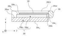
次に、図5Aから図5Cを参照して、本開示の実施形態1の変形例3におけるレーザ光源130の構成例を説明する。図5Aは、本開示の実施形態1の変形例3におけるレーザ光源130の構成例を模式的に示す斜視図である。図5Bは、図5Aのレーザ光源130を模式的に示す上面図である。図5Cは、図5Bの構成のYZ平面に平行なVC-VC線断面図である。実施形態1の変形例3におけるレーザ光源130が実施形態1におけるレーザ光源100と異なる点は、サブマウント20の構成である。実施形態1の変形例3におけるサブマウント20は、第1のサブマウント部分20pと、第2のサブマウント部分20pとを含む。第1のサブマウント部分20pは、一対のレンズ支持部20LSを上面20usに有する。第1のサブマウント部分20pは、Z方向に延びる前述したU字型形状を有する。第1のサブマウント部分20pは、例えばAlN、SiC、およびアルミナからなる群から選択される少なくとも1つを含むセラミックおよびCuWなどの合金から形成され得る。第2のサブマウント部分20pは、第1のサブマウント部分20pの上面20usに固定され、一対のレンズ支持部20LSの間に位置する。第2のサブマウント部分20pは、レーザダイオードチップ10を搭載する主平面20sと、コリメートレンズ30に対向する前方端面20feとを有する。主平面20sは、第1のサブマウント部分20pのうち、上面20usに固定された面とは反対の側の面である。本開示において、前方端面20feと裏面20sとは直接つながる必要はない。本開示では、前方端面20feの一辺と、主平面20sの一辺とが接触しており、前方端面20feと主平面20sとが接触した一辺が、主平面20sのエッジ20edを規定する。第2のサブマウント部分20pの熱伝導率が、第1のサブマウント部分20pの熱伝導率よりも高ければ、レーザダイオードチップ10から発せられた熱を効率よく外部に伝えることができる。第2のサブマウント部分20pは、例えばCu、Al、Ag、Fe、Ni、Mo、Cu、W、CuW、CuMo、AlN、SiCおよびアルミナからなる群から選択される少なくとも1つから形成され得る。第2のサブマウント部分20pのX方向におけるサイズは、例えば0.5mm以上1.5mm以下であり、Y方向におけるサイズは、例えば0.1mm以上0.5mm以下であり、Z方向におけるサイズは、例えば1mm以上6mm以下である。 Next, with reference to FIG. 5A to FIG. 5C, a configuration example of thelaser light source 130 in the modified example 3 of theembodiment 1 of the present disclosure will be described. FIG. 5A is a perspective view that shows a schematic configuration example of thelaser light source 130 in the modified example 3 of theembodiment 1 of the present disclosure. FIG. 5B is a top view that shows a schematic configuration of thelaser light source 130 in FIG. 5A. FIG. 5C is a VC-VC line cross-sectional view parallel to the YZ plane of the configuration of FIG. 5B. Thelaser light source 130 in the modified example 3 of theembodiment 1 differs from thelaser light source 100 in theembodiment 1 in the configuration of thesubmount 20. Thesubmount 20 in the modified example 3 of theembodiment 1 includes a first submount portion 20p1 and a second submount portion 20p2. The first submount portion 20p1 has a pair of lens support portions 20LS on the upper surface 20us. The first submount portion 20p1 has the above-mentioned U-shaped shape extending in the Z direction. The first submount portion 20p1 may be formed of, for example, a ceramic including at least one selected from the group consisting of AlN, SiC, and alumina, and an alloy such as CuW. The second submount portion 20p2 is fixed to the upper surface 20us of the first submount portion 20p1 and is located between a pair of lens supports 20LS. The second submount portion 20p2 has amain plane 20s1 on which thelaser diode chip 10 is mounted, and a front end surface 20fe facing the collimatinglens 30. Themain plane 20s1 is the surface of the first submount portion 20p1 opposite to the surface fixed to the upper surface 20us. In the present disclosure, the front end surface 20fe and theback surface 20s2 do not need to be directly connected. In the present disclosure, one side of the front end face 20fe is in contact with one side of the main plane20s1 , and the side where the front end face 20fe is in contact with the main plane20s1 defines the edge 20ed of the main plane20s1 . If the thermal conductivity of the second submount portion20p2 is higher than that of the first submount portion20p1 , the heat generated from thelaser diode chip 10 can be efficiently transferred to the outside. The second submount portion20p2 can be formed of at least one selected from the group consisting of, for example, Cu, Al, Ag, Fe, Ni, Mo, Cu, W, CuW, CuMo, AlN, SiC, and alumina. The size of the second submount portion20p2 in the X direction is, for example, 0.5 mm to 1.5 mm, the size in the Y direction is, for example, 0.1 mm to 0.5 mm, and the size in the Z direction is, for example, 1 mm to 6 mm.

このサブマウント20では、別体である第1のサブマウント部分20pおよび第2のサブマウント部分20pにより、第1のサブマウント部分20p上で第2のサブマウント部分20pの位置を調整することができる。このサブマウント20のように、主平面20sを有する部分と、一対のレンズ支持部20LSを有する部分とが別体になっていてもよい。このサブマウント20では、一対のレンズ支持部20LSのそれぞれと第2のサブマウント部分20pとの間には、空隙20gが存在する。空隙20gのX方向におけるサイズは、例えば50μm以上300μm以下である。空隙20gのY方向およびZ方向におけるサイズは、それぞれ、第2のサブマウント部分20pのY方向およびZ方向におけるサイズによって決まる。空隙20gにより、実施形態1の変形例2におけるレーザ光源120と同様に、コリメートレンズ30と一対のレンズ支持部20LSの端面20seとの接合時における熱がレーザダイオードチップ10に与える影響を低減することができる。 In thissubmount 20, the position of the second submount portion20p2 can be adjusted on the first submount portion 20p1by the first submount portion20p1 and the second submount portion20p2 , which are separate bodies. As in thissubmount 20, a portion having a main plane20s1 and a portion having a pair of lens support portions 20LS may be separate bodies. In thissubmount 20, agap 20g exists between each of the pair of lens support portions 20LS and the second submount portion20p2 . The size of thegap 20g in the X direction is, for example, 50 μm or more and 300 μm or less. The sizes of thegap 20g in the Y direction and the Z direction are determined by the sizes of the second submount portion20p2 in the Y direction and the Z direction, respectively. As with thelaser light source 120 in variant example 2 ofembodiment 1, thegap 20g can reduce the effect that heat has on thelaser diode chip 10 when thecollimator lens 30 is joined to the end faces 20se of a pair of lens support parts 20LS.

次に、図6Aから図6Cを参照して、本開示の実施形態1の変形例4におけるレーザ光源140の構成例を説明する。図6Aは、本開示の実施形態1の変形例4におけるレーザ光源140の構成例を模式的に示す斜視図である。図6Aでは、レーザダイオードチップ10と、サブマウント20と、コリメートレンズ30とが分離された状態で記載されているが、実際にはこれらは接合されている。図6Bは、図6Aのレーザ光源140を模式的に示す上面図である。図6Cは、図6Bの構成のYZ平面に平行なVIC-VIC線断面図である。実施形態1の変形例4におけるレーザ光源140が実施形態1におけるレーザ光源100と異なる点は、サブマウント20の構成である。実施形態1の変形例4におけるサブマウント20は、主平面20sから裏面20sに達する貫通孔20hと、貫通孔20hを埋める金属20mとを有している。このサブマウント20の貫通孔20h以外の部分は、例えばセラミックから形成され得る。金属20mは、高い熱伝導率を有し、例えばCu、Al、Ag、Fe、Ni、Mo、Cu、W、およびCuMoからなる群から選択される少なくとも1つを含み得る。金属20mのX方向における最大のサイズは、例えば0.5mm以上1.5mm以下であり、Z方向における最大のサイズは、例えば1mm以上6mm以下である。金属20mは、上面視で、レーザダイオードチップ10にすべてが重なっていてもよいし、一部が重なっていてもよい。レーザダイオードチップ10をサブマウント20における金属20mに接触して配置することにより、レーザダイオードチップ10から発せられた熱を、金属20mを介して半導体レーザパッケージ40に効率よく伝えることができる。 Next, referring to FIG. 6A to FIG. 6C, a configuration example of thelaser light source 140 in the modified example 4 of theembodiment 1 of the present disclosure will be described. FIG. 6A is a perspective view that shows a schematic configuration example of thelaser light source 140 in the modified example 4 of theembodiment 1 of the present disclosure. In FIG. 6A, thelaser diode chip 10, thesubmount 20, and thecollimator lens 30 are shown in a separated state, but in reality, they are joined together. FIG. 6B is a top view that shows thelaser light source 140 in FIG. 6A. FIG. 6C is a cross-sectional view of the VIC-VIC line parallel to the YZ plane of the configuration of FIG. 6B. Thelaser light source 140 in the modified example 4 of theembodiment 1 differs from thelaser light source 100 in theembodiment 1 in the configuration of thesubmount 20. Thesubmount 20 in the modified example 4 of theembodiment 1 has a throughhole 20h that reaches theback surface 20s2 from themain plane 20s1 , and ametal 20m that fills the throughhole 20h. The portion of thesubmount 20 other than the throughhole 20h can be formed of, for example, ceramic. Themetal 20m has a high thermal conductivity and may include at least one selected from the group consisting of Cu, Al, Ag, Fe, Ni, Mo, Cu, W, and CuMo. The maximum size of themetal 20m in the X direction is, for example, 0.5 mm or more and 1.5 mm or less, and the maximum size in the Z direction is, for example, 1 mm or more and 6 mm or less. Themetal 20m may entirely overlap thelaser diode chip 10 in a top view, or may overlap only a part of it. By disposing thelaser diode chip 10 in contact with themetal 20m in thesubmount 20, the heat generated from thelaser diode chip 10 can be efficiently transferred to thesemiconductor laser package 40 via themetal 20m.

次に、図7Aから図7Cを参照して、本開示の実施形態1の変形例5におけるレーザ光源150の構成例を説明する。図7Aは、本開示の実施形態1の変形例5におけるレーザ光源150の構成例を模式的に示す斜視図である。図7Bは、図7Aのレーザ光源150を模式的に示す上面図である。図7Cは、図7Bの構成のYZ平面に平行なVIIC-VIIC線断面図である。実施形態1の変形例5におけるレーザ光源150が実施形態1におけるレーザ光源100と異なる点は、コリメートレンズ30の形状である。実施形態1の変形例5におけるコリメートレンズ30は、一対の平坦部30f、および一対の平坦部30fによって挟まれたレンズ曲面部30cを有する。実施形態1の変形例5におけるレンズ曲面部30cは、実施形態1におけるコリメートレンズ30と同様に、FACレンズとして機能する。Next, with reference to Figures 7A to 7C, a configuration example of thelaser light source 150 in Modification 5 of theembodiment 1 of the present disclosure will be described. Figure 7A is a perspective view that shows a schematic configuration example of thelaser light source 150 in Modification 5 of theembodiment 1 of the present disclosure. Figure 7B is a top view that shows a schematic configuration example of thelaser light source 150 in Figure 7A. Figure 7C is a VIIC-VIIC line cross-sectional view parallel to the YZ plane of the configuration in Figure 7B. Thelaser light source 150 in Modification 5 of theembodiment 1 differs from thelaser light source 100 in theembodiment 1 in the shape of thecollimator lens 30. Thecollimator lens 30 in Modification 5 of theembodiment 1 has a pair offlat portions 30f and a lenscurved portion 30c sandwiched between the pair offlat portions 30f. The lens curvedportion 30c in Modification 5 of theembodiment 1 functions as an FAC lens, similar to thecollimator lens 30 in theembodiment 1.

次に、図7Dを参照して、コリメートレンズ30における一対の平坦部30fの利点を説明する。図7Dは、コレット60を用いて、図7Aのレーザ光源150におけるコリメートレンズ30をサブマウント20に接合する様子を模式的に示す斜視図である。コレット60は、二又部分60aおよび二又部分60aに接続された支持部分60bを有する。コレット60は中空構造を有し、コリメートレンズ30を吸着して支持することができる。具体的には、コレット60における二又部分60aの先端部が、コリメートレンズ30における一対の平坦部30fを吸着する。実装装置によって支持部分60bを保持し、二又部分60aによってコリメートレンズ30を支持しながら、そのコリメートレンズ30をサブマウント20に接合することにより、一対のレンズ支持部20LSの端面20seに対して垂直な方向に、安定して荷重をかけることができる。荷重をかけた状態で、コリメートレンズ30と一対のレンズ支持部20LSの端面20seとの間の接合材が加熱される。Next, referring to FIG. 7D, the advantages of the pair offlat portions 30f in thecollimating lens 30 will be described. FIG. 7D is a perspective view that shows a schematic view of the collimatinglens 30 in thelaser light source 150 in FIG. 7A being bonded to thesubmount 20 using thecollet 60. Thecollet 60 has abifurcated portion 60a and asupport portion 60b connected to thebifurcated portion 60a. Thecollet 60 has a hollow structure and can support the collimatinglens 30 by adsorption. Specifically, the tip of thebifurcated portion 60a in thecollet 60 adsorbs the pair offlat portions 30f in thecollimating lens 30. By holding thesupport portion 60b by the mounting device and supporting the collimatinglens 30 by thebifurcated portion 60a, and bonding thecollimating lens 30 to thesubmount 20, a load can be applied stably in a direction perpendicular to the end faces 20se of the pair of lens support portions 20LS. With the load applied, the bonding material between thecollimator lens 30 and the end faces 20se of the pair of lens support portions 20LS is heated.

コレット60における二又部分60aの間に不図示のミラーを設けてもよい。レーザダイオードチップ10からレーザ光をZ方向に出射させながらコリメートレンズ30をサブマウント20に接合し、不図示のミラーによってY方向に反射されたレーザ光を受光装置によって受けることにより、コリメートレンズ30とレーザダイオードチップ10の出射端面10eとの位置合わせを精度よく行うことができる。受光装置は、例えば、パワーメータ、平行度測定器、または、ビームプロファイラであり得る。 A mirror (not shown) may be provided between thebifurcated portions 60a of thecollet 60. Thecollimator lens 30 is bonded to thesubmount 20 while emitting laser light in the Z direction from thelaser diode chip 10, and the laser light reflected in the Y direction by a mirror (not shown) is received by a light receiving device, thereby enabling accurate alignment of thecollimator lens 30 with theemission end surface 10e-1 of thelaser diode chip 10. The light receiving device may be, for example, a power meter, a parallelism measuring device, or a beam profiler.

(実施形態2)
次に、図8Aから図8Dを参照して、本開示の実施形態2におけるレーザ光源の基本的な構成例を説明する。
(Embodiment 2)
Next, a basic configuration example of a laser light source according to the second embodiment of the present disclosure will be described with reference to FIGS. 8A to 8D.

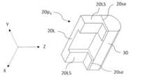
図8Aは、本開示の実施形態2におけるレーザ光源200の構成例を模式的に示す斜視図である。図8Bは、図8Aのレーザ光源200を模式的に示す上面図である。図8Cは、図8Bの構成のYZ平面に平行なVIIIC-VIIIC線断面図である。図8Dは、図8Aのレーザ光源200を模式的に示す背面図である。実施形態2におけるレーザ光源200が実施形態1におけるレーザ光源100と異なる点は、サブマウント20の構成である。実施形態2におけるサブマウント20は、第3のサブマウント部分20pと、第4のサブマウント部分20pとを含む。第3のサブマウント部分20pは、主平面20s、裏面20s、および前方端面20feを有する。第4のサブマウント部分20pは、第3のサブマウント部分20pの主平面20sに固定される一対のレンズ支持部20LS、および一対のレンズ支持部20LSを連結する連結部20Lを有する。連結部20Lは、レーザダイオードチップ10の出射端面10eから出射されるレーザ光の伝搬を妨げないように一対のレンズ支持部20LSを連結する。このサブマウント20では、第3のサブマウント部分20p、および第4のサブマウント部分20pが別体になっている。このサブマウント20のように、主平面20sを有する部分と、一対のレンズ支持部20LSを有する部分とが別体になっていてもよい。図8Aでは、第3のサブマウント部分20p、第4のサブマウント部分20p、およびコリメートレンズ30は分離された状態で記載されているが、実際にはこれらは接合されている。第4のサブマウント部分20pにおける一対のレンズ支持部20LS、および連結部20Lは一体成型されている。 FIG. 8A is a perspective view that shows a schematic configuration example of thelaser light source 200 in the second embodiment of the present disclosure. FIG. 8B is a top view that shows thelaser light source 200 in FIG. 8A. FIG. 8C is a cross-sectional view of the configuration of FIG. 8B taken along line VIIIC-VIIIC parallel to the YZ plane. FIG. 8D is a rear view that shows thelaser light source 200 in FIG. 8A. Thelaser light source 200 in the second embodiment differs from thelaser light source 100 in the first embodiment in the configuration of thesubmount 20. Thesubmount 20 in the second embodiment includes a third submount portion 20p3 and a fourth submount portion 20p4. The third submount portion 20p3 has amain plane 20s1 , aback surface 20s2 , and a front end surface 20fe. The fourth submount portion20p4 has a pair of lens support portions 20LS fixed to the main plane20s1 of the third submount portion20p3 , and a connectingportion 20L connecting the pair of lens support portions 20LS. The connectingportion 20L connects the pair of lens support portions 20LS so as not to impede the propagation of the laser light emitted from the emission end surface10e1 of thelaser diode chip 10. In thissubmount 20, the third submount portion20p3 and the fourth submount portion20p4 are separate. As in thissubmount 20, the portion having the main plane20s1 and the portion having the pair of lens support portions 20LS may be separate. In FIG. 8A, the third submount portion20p3 , the fourth submount portion20p4 , and thecollimating lens 30 are shown in a separated state, but in reality, they are joined together. The pair of lens support portions 20LS and the connectingportion 20L in the fourth submount portion20p4 are integrally molded.

図8Bおよび図8Cに示すように、連結部20Lは、上面視で、レーザダイオードチップ10の出射端面10eと重なる。図8Dに示すように、第4のサブマウント部分20pは、レーザダイオードチップ10を跨ぐように第3のサブマウント部分20pの主平面20sに配置されている。第4のサブマウント部分20pのX方向におけるサイズは、第3のサブマウント部分20pのX方向におけるサイズよりも大きいので、一対のレンズ支持部20LSの端面20seの面積を広くすることができる。その結果、コリメートレンズ30を一対のレンズ支持部20LSの端面20seに接合することが容易になる。第4のサブマウント部分20pの一対のレンズ支持部20LSのY方向におけるサイズは、コリメートレンズ30のY方向におけるサイズと同程度であり得る。第4のサブマウント部分20pの一対のレンズ支持部20LSのY方向におけるサイズは、コリメートレンズ30のY方向におけるサイズよりも大きくてもよいし、等しくてもよいし、小さくてもよい。第4のサブマウント部分20pのX方向におけるサイズは、例えば0.5mm以上4mm以下であり、Y方向における最大のサイズは、例えば0.5mm以上2mm以下であり、Z方向におけるサイズは、例えば0.5mm以上1mm以下である。 As shown in FIG. 8B and FIG. 8C, the connectingportion 20L overlaps with theemission end surface 10e1 of thelaser diode chip 10 in a top view. As shown in FIG. 8D, the fourth submount portion 20p4 is disposed on themain plane 20s1 of the third submount portion 20p3 so as to straddle thelaser diode chip 10. Since the size of the fourth submount portion 20p4 in the X direction is larger than the size of the third submount portion 20p3 in the X direction, the area of the end surface 20se of the pair of lens support portions 20LS can be made larger. As a result, it becomes easier to bond the collimatinglens 30 to the end surface 20se of the pair of lens support portions 20LS. The size of the pair of lens support portions 20LS of the fourth submount portion 20p4 in the Y direction can be approximately the same as the size of the collimatinglens 30 in the Y direction. The size in the Y direction of the pair of lens support portions 20LS ofthe fourth submount portion 20p4 may be larger than, equal to, or smaller than the size in the Y direction of thecollimator lens 30. The size in the X direction ofthe fourth submount portion 20p4 is, for example, 0.5 mm or more and 4 mm or less, the maximum size in the Y direction is, for example, 0.5 mm or more and 2 mm or less, and the size in the Z direction is, for example, 0.5 mm or more and 1 mm or less.

実施形態2におけるレーザ光源200の作製では、第3のサブマウント部分20pの主平面20sにレーザダイオードチップ10を接合する工程と、レーザダイオードチップ10を跨ぐように第3のサブマウント部分20pの主平面20sに第4のサブマウント部分20pを接合する工程と、第4のサブマウント部分20pにおける一対のレンズ支持部20LSの端面20seにコリメートレンズ30を接合する工程とを、この順で実行してもよい。あるいは、レーザダイオードチップ10が主平面20sに接合された第3のサブマウント部分20pに、コリメートレンズ30が接合された第4のサブマウント部分20pを接合してもよい。 In the fabrication of thelaser light source 200 in the second embodiment, a step of bonding thelaser diode chip 10 to the main plane20s1 of thethird submount portion20p3 , a step of bonding the fourth submount portion20p4 to the main plane20s1 of the third submount portion 20p3 so as to straddle thelaser diode chip 10, and a step of bonding thecollimator lens 30 to the end faces 20se of the pair of lens support portions20LS in the fourth submount portion 20p4 may be performed in this order. Alternatively, the fourth submount portion20p4 to which the collimator lens30 is bonded may be bonded to the third submount portion 20p3 to which the laser diode chip10 is bonded to the main plane 20s1.

実施形態2におけるレーザ光源200では、実施形態1におけるレーザ光源100と同様に、サブマウント20が、一対のレンズ支持部20LSの間の主平面20sによってレーザダイオードチップ10を支持し、一対のレンズ支持部20LSの端面20seによってコリメートレンズ30を支持している。これにより、レーザダイオードチップ10とコリメートレンズ30との位置合わせが容易になり、小型のレーザ光源200を実現することが可能になる。さらに、実施形態2におけるレーザ光源200では、実施形態1におけるレーザ光源100と同様に、レーザダイオードチップ10がサブマウント20にフェイスダウンの状態で配置されても、接合材がレーザダイオードチップ10の出射端面10eにせり上がることを抑制することができる。 In thelaser light source 200 in the second embodiment, similarly to thelaser light source 100 in the first embodiment, thesubmount 20 supports thelaser diode chip 10 by the main plane20s1 between the pair of lens support parts 20LS, and supports thecollimator lens 30 by the end face 20se of the pair of lens support parts 20LS. This makes it easy to align thelaser diode chip 10 and thecollimator lens 30, and makes it possible to realize a compactlaser light source 200. Furthermore, in thelaser light source 200 in the second embodiment, similarly to thelaser light source 100 in the first embodiment, even if thelaser diode chip 10 is placed face-down on thesubmount 20, it is possible to prevent the bonding material from rising up to the emission end face10e1 of thelaser diode chip 10.

(実施形態2の変形例)
次に、本開示の実施形態2におけるレーザ光源200の変形例1および変形例2を説明する。前述と重複する説明は省略することがある。
(Modification of the second embodiment)
Next, modified example 1 and modified example 2 of thelaser light source 200 according to the second embodiment of the present disclosure will be described. Descriptions that overlap with those described above may be omitted.

図9Aから図9Dを参照して、本開示の実施形態2の変形例1におけるレーザ光源210の構成例を説明する。図9Aは、本開示の実施形態2の変形例1におけるレーザ光源210の構成例を模式的に示す斜視図である。図9Bは、図9Aのレーザ光源210を模式的に示す上面図である。図9Cは、図9Bの構成のYZ平面に平行なIXC-IXC線断面図である。図9Dは、図9Aのレーザ光源210を模式的に示す背面図である。実施形態2の変形例1におけるレーザ光源210が実施形態2におけるレーザ光源200と異なる点は、サブマウント20における第4のサブマウント部分20pの形状である。実施形態2の変形例1における第4のサブマウント部分20pは、実施形態2における第4のサブマウント部分20pにおいて、一対のレンズ支持部20LSの間に切り欠き20coを有する。切り欠き20coにより、図9Bおよび図9Cに示すように、連結部20Lは、上面視で、レーザダイオードチップ10の出射端面10eとは重ならない。切り欠き20coのX方向におけるサイズは、例えば0.2mm以上3mm以下であり、Z方向におけるサイズは、例えば0.5mm以上1mm以下である。切り欠き20coのZ方向におけるサイズは、一対のレンズ支持部20LSの端面20seと、第3のサブマウント部分20pにおける主平面20sのエッジ20edとのZ方向におけるサイズよりも大きい。実施形態2の変形例1におけるレーザ光源210の作製では、切り欠き20coを通じて、レーザダイオードチップ10の出射端面10eと、第4のサブマウント部分20pとの位置合わせ、および、レーザダイオードチップ10の出射端面10eと、コリメートレンズ30との位置合わせが容易になる。 A configuration example of thelaser light source 210 inModification 1 of the embodiment 2 of the present disclosure will be described with reference to FIGS. 9A to 9D. FIG. 9A is a perspective view that shows a schematic configuration example of thelaser light source 210 inModification 1 of the embodiment 2 of the present disclosure. FIG. 9B is a top view that shows a schematic configuration example of thelaser light source 210 in FIG. 9A. FIG. 9C is a cross-sectional view of the configuration of FIG. 9B along the line IXC-IXC parallel to the YZ plane. FIG. 9D is a rear view that shows a schematic configuration example of thelaser light source 210 in FIG. 9A. Thelaser light source 210 inModification 1 of the embodiment 2 differs from thelaser light source 200 in the embodiment 2 in the shape of the fourth submount portion20p4 in the submount20. The fourth submount portion 20p4 inModification 1 of the embodiment 2 has a notch 20co between a pair of lens support portions 20LS in the fourth submount portion20p4 in the embodiment 2. As shown in FIG. 9B and FIG. 9C, the notch 20co prevents thecoupling portion 20L from overlapping theemission end surface 10e1 of thelaser diode chip 10 in top view. The size of the notch 20co in the X direction is, for example, 0.2 mm or more and 3 mm or less, and the size in the Z direction is, for example, 0.5 mm or more and 1 mm or less. The size of the notch 20co in the Z direction is larger than the size in the Z direction between the end surfaces 20se of the pair of lens supports 20LS and the edge 20ed of themain plane 20s1 in the third submount portion 20p3. In the manufacture of thelaser light source 210 in the first modification of the second embodiment, the notch 20co facilitates the alignment of theemission end surface 10e1 of thelaser diode chip 10 with the fourth submount portion 20p4 , and the alignment of theemission end surface 10e1 of thelaser diode chip 10 with thecollimator lens 30.

次に、図10Aから図10Dを参照して、本開示の実施形態2の変形例2におけるレーザ光源220の構成例を説明する。図10Aは、本開示の実施形態2の変形例2におけるレーザ光源220の構成例を模式的に示す斜視図である。図10Bは、図10Aのレーザ光源220を模式的に示す上面図である。図10Cは、図10Bの構成のYZ平面に平行なXC-XC線断面図である。図10Dは、図10Aに示す第4のサブマウント部分20pおよびコリメートレンズ30を模式的に示す斜視図である。実施形態2の変形例2におけるレーザ光源220が実施形態2におけるレーザ光源200と異なる点は、サブマウント20における第4のサブマウント部分20p、およびコリメートレンズ30である。図10Dに示すように、実施形態2の変形例2における第4のサブマウント部分20p、およびコリメートレンズ30は一体成型されている。第4のサブマウント部分20pおよびコリメートレンズ30を接合する必要がないので、実施形態2の変形例2における第4のサブマウント部分20pのX方向におけるサイズは、実施形態2における第4のサブマウント部分20pのX方向におけるサイズほど大きくなくてもよい。実施形態2の変形例2における第4のサブマウント部分20pのX方向におけるサイズは、例えば0.2mm以上3mm以下であり、Y方向における最大のサイズは、例えば0.3mm以上1mm以下であり、Z方向におけるサイズは、例えば0.5mm以上1mm以下である。 Next, with reference to Figs. 10A to 10D, a configuration example of thelaser light source 220 in Modification 2 of the embodiment 2 of the present disclosure will be described. Fig. 10A is a perspective view that shows a schematic configuration example of thelaser light source 220 in Modification 2 of the embodiment 2 of the present disclosure. Fig. 10B is a top view that shows a schematic configuration example of thelaser light source 220 in Fig. 10A. Fig. 10C is a cross-sectional view of the XC-XC line parallel to the YZ plane of the configuration in Fig. 10B. Fig. 10D is a perspective view that shows a schematic configuration example of the fourth submount portion 20p4 and thecollimator lens 30 shown in Fig. 10A. Thelaser light source 220 in Modification 2 of the embodiment 2 is different from thelaser light source 200 in the embodiment 2 in the fourth submount portion 20p4 in thesubmount 20 and thecollimator lens 30. As shown in Fig. 10D, the fourth submount portion 20p4 and thecollimator lens 30 in Modification 2 of the embodiment 2 are integrally molded. Since there is no need to bond the fourth submount portion20p4 and thecollimator lens 30, the size in the X direction of the fourth submount portion20p4 in the second modification of the second embodiment does not need to be as large as the size in the X direction of the fourth submount portion20p4 in the second embodiment. The size in the X direction of the fourth submount portion20p4 in the second modification of the second embodiment is, for example, 0.2 mm or more and 3 mm or less, the maximum size in the Y direction is, for example, 0.3 mm or more and 1 mm or less, and the size in the Z direction is, for example, 0.5 mm or more and 1 mm or less.

一体成型された第4のサブマウント部分20pおよびコリメートレンズ30は、例えば、ガラス、石英、合成石英、サファイア、透明セラミック、およびプラスチックの少なくとも1つから形成され得る。一体成型された第4のサブマウント部分20pおよびコリメートレンズ30が透明である場合、レーザダイオードチップ10の出射端面10eと、コリメートレンズ30との位置合わせが容易になる。 The integrally molded fourth submount portion20p4 and thecollimating lens 30 may be made of at least one of glass, quartz, synthetic quartz, sapphire, transparent ceramic, and plastic. If the integrally molded fourth submount portion20p4 and thecollimating lens 30 are transparent, alignment between the emission end surface10e1 of thelaser diode chip 10 and thecollimating lens 30 becomes easy.

前述した実施形態およびその変形例における構成要素を任意に組み合わせてもよい。The components in the above-described embodiments and their variations may be combined in any manner.

(応用例)
本開示のレーザ光源は、例えば、複数のレーザビームを結合して出力を高めるダイレクトダイオードレーザの光源として用いられ得る。ビーム結合は、複数のレーザ光源から出射されたレーザビームを正確に結合することによって行われる。波長が570nm以下の高強度のレーザビームによれば、例えば銅などの金属をも加工することが容易になる。本開示のレーザ光源では、レーザダイオードチップとレンズとの位置ずれが生じにくいので、レーザ光源から外部に出射されるレーザ光の光軸の向きが大きくずれることはない。複数のレーザ光源から出射されたレーザビームを正確に結合させ、ビーム品質を高めることが可能になる。
(Application example)
The laser light source of the present disclosure can be used, for example, as a light source of a direct diode laser that combines multiple laser beams to increase output. The beam combination is performed by accurately combining the laser beams emitted from multiple laser light sources. A high-intensity laser beam with a wavelength of 570 nm or less makes it easy to process metals such as copper. In the laser light source of the present disclosure, the positional deviation between the laser diode chip and the lens is unlikely to occur, so that the direction of the optical axis of the laser light emitted to the outside from the laser light source does not deviate significantly. It is possible to accurately combine the laser beams emitted from multiple laser light sources and improve the beam quality.

本開示のレーザ光源は、例えば、プロジェクタ、および照明器具にも利用され得る。The laser light sources disclosed herein may also be used, for example, in projectors and lighting fixtures.

10 レーザダイオードチップ
10a 半導体積層構造体
10b 基板
10C 第1のクラッド層
10C 第2のクラッド層
10e 出射端面
10e 後方端面
10L 発光層
20 サブマウント
20co 切り欠き
20d 溝
20ed エッジ
20fe 前方端面
20fe 中央端面
20fe 両側端面
20L 連結部
20LS レンズ支持部
20p 第1のサブマウント部分
20p 第2のサブマウント部分
20p 第3のサブマウント部分
20p 第4のサブマウント部分
20s 主平面
20s 裏面
20se 一対のレンズ支持部の端面
20us 第1のサブマウント部分の上面
30 コリメートレンズ
30c レンズ曲面部
30f 平坦部
40 半導体レーザパッケージ
40b 基体
40L 蓋体
40w 透光窓
50 リード端子
60 コレット
60a 二又部分
60b 支持部分
100、110、120、130、140、150 レーザ光源
200、210、220 レーザ光源
10Laser diode chip 10a Semiconductor laminatedstructure 10b Substrate 10C1 First cladding layer 10C2Second cladding layer 10e1Emission end surface 10e2Rear end surface 10LLight emitting layer 20Submount 20co Notch 20d Groove 20ed Edge 20fe Front end surface 20fe1 Center end surface 20fe2 Both side end surfaces 20L Connection portion 20LS Lens support portion 20p1 First submount portion 20p2 Second submount portion 20p3 Third submount portion 20p4Fourth submount portion 20s1 Main plane 20s2 Rear surface 20se End surfaces of a pair of lens support portions 20us Upper surface offirst submount portion 30Collimating lens 30c Lens curvedsurface portion 30fFlat portion 40Semiconductor laser package40b Base body40L Lid body 40w Light-transmittingwindow 50Lead terminal 60Collet 60a Forkedportion60b Support portion 100, 110, 120, 130, 140, 150 Laserlight source 200, 210, 220 Laser light source

Claims (14)

Translated fromJapanese
発光層を含む半導体積層構造体と、前記半導体積層構造体を支持する基板と、前記発光層で発生したレーザ光を出射する第1の端面と、前記第1の端面とは反対側の第2の端面と、を有し、前記第1の端面から前記第2の端面までの距離によって共振器長が規定される、端面出射型のレーザダイオードチップと、
前記レーザダイオードチップが固着された主平面と、前記レーザダイオードチップの前記第1の端面の両側に位置する一対のレンズ支持部と、前記レーザダイオードチップの前記第1の端面から出射される前記レーザ光の伝搬を妨げないように前記一対のレンズ支持部を連結し、上面視で、前記レーザダイオードチップの前記第1の端面と重なる連結部と、前記主平面の反対側に位置する裏面と、を持つサブマウントと、
前記一対のレンズ支持部の端面と接合されたレンズと、
前記レーザダイオードチップ、前記レンズ、および前記サブマウントを収容する半導体レーザパッケージと、
を備え、
前記発光層が、前記レーザダイオードチップの前記基板と比較して、前記サブマウントに近い状態で、前記レーザダイオードチップが前記サブマウントに固着されており、
前記レーザダイオードチップの前記第1の端面は、前記主平面のエッジよりも前記共振器長の方向に突出し、
前記一対のレンズ支持部の前記端面は、前記レーザダイオードチップの前記第1の端面よりも前記共振器長の方向に突出
前記一対のレンズ支持部、および前記連結部は一体成型されている、レーザ光源。
an edge-emitting laser diode chip having a semiconductor laminated structure including a light-emitting layer, a substrate supporting the semiconductor laminated structure, a first end face for emitting laser light generated in the light-emitting layer, and a second end face opposite to the first end face, the edge-emitting laser diode chip having a cavity length defined by a distance from the first end face to the second end face;
a submount having a main plane to which the laser diode chip is fixed, a pair of lens support parts located on both sides of the first end faceof the laser diode chip, a connection part that connects the pair of lens support parts so as not to interfere with the propagation of the laser light emitted from the first end face of the laser diode chip and overlaps with the first end face of the laser diode chip in a top view, and a back surface located on the opposite side of the main plane;
a lens bonded to the end faces of the pair of lens support parts;
a semiconductor laser package housing the laser diode chip, the lens, and the submount;
Equipped with
the laser diode chip is fixed to the submount with the light emitting layer being closer to the submount than the substrate of the laser diode chip;
the first end face of the laser diode chip protrudes beyond an edge of the main plane in a direction of the cavity length;
the end faces of the pair of lens support partsprotrude in the direction of the cavity length beyond the first end face of the laser diode chip,
The pair of lens support portions and the connecting portion are integrally molded.
前記半導体レーザパッケージは、前記サブマウントの前記裏面に熱的に接触する基体を有し、前記レーザダイオードチップ、前記サブマウント、および前記レンズを気密に封止している、請求項1に記載のレーザ光源。The laser light source according to claim 1, wherein the semiconductor laser package has a base that is in thermal contact with the back surface of the submount and hermetically seals the laser diode chip, the submount, and the lens. 前記サブマウントは、前記主平面および前記裏面をつなぐ前方端面を有し、
前記前方端面は、中央端面、および前記中央端面の両側に位置する両側端面を有し、
前記中央端面は、前記両側端面よりも前記共振器長の方向に窪み、
前記主平面の前記エッジは、前記サブマウントにおける前記主平面と前記中央端面とによって規定される、請求項1または2に記載のレーザ光源。
the submount has a front end surface connecting the main plane and the back surface;
The front end surface has a central end surface and side end surfaces located on both sides of the central end surface,
the central end face is recessed in a direction of the cavity length from the both side end faces,
The laser light source according to claim 1 , wherein the edge of the main plane is defined by the main plane and the central end face of the submount.
前記サブマウントは、前記一対のレンズ支持部のそれぞれと前記レーザダイオードチップとの間に、前記共振器長の方向に沿って延びる溝を有している、請求項1または2に記載のレーザ光源。The laser light source according to claim 1 or 2, wherein the submount has a groove extending along the direction of the cavity length between each of the pair of lens supports and the laser diode chip. 前記レンズは、無機材料によって、前記一対のレンズ支持部の前記端面に接合されている、請求項1からのいずれか一項に記載のレーザ光源。 The laser light source according to claim1 , wherein the lens is bonded to the end faces of the pair of lens support parts by an inorganic material. 前記サブマウントの一部または全体は、セラミックから形成されている、請求項1からのいずれか一項に記載のレーザ光源。 The laser light source according to claim1 , wherein a part or the whole of the submount is made of ceramic. 前記サブマウントは、前記主平面から前記裏面に達する貫通孔と、前記貫通孔を埋める金属とを有している、請求項に記載のレーザ光源。 The laser light source according to claim6 , wherein the submount has a through hole extending from the main surface to the rear surface, and a metal filling the through hole. 前記共振器長の方向から見たとき、前記レンズの重心は前記一対のレンズ支持部の間に位置する、請求項1からのいずれか一項に記載のレーザ光源。 The laser light source according to claim1 , wherein a center of gravity of the lens is located between the pair of lens support parts when viewed from the direction of the resonator length. 前記レーザ光の波長は、350nm以上570nm以下である、請求項1からのいずれか一項に記載のレーザ光源。 The laser light source according to claim1 , wherein the wavelength of the laser light is not less than 350 nm and not more than 570 nm. 前記レンズは、前記主平面の法線方向および前記共振器長の方向の両方に垂直な方向に沿って延びる構造を有し、
前記レンズは、前記主平面の法線方向および前記共振器長の方向の両方を含む平面内における前記レーザ光の発散角を低減する、請求項1からのいずれか一項に記載のレーザ光源。
the lens has a structure extending along a direction perpendicular to both a normal direction of the principal plane and a direction of the cavity length,
The laser light source according to claim1 , wherein the lens reduces a divergence angle of the laser light in a plane including both a normal direction to the principal plane and a direction of the cavity length.
前記レンズは、一対の平坦部、および前記一対の平坦部によって挟まれたレンズ曲面部を有する、請求項1から10のいずれか一項に記載のレーザ光源。 The laser light source according to claim1 , wherein the lens has a pair of flat portions and a lens curved surface portion sandwiched between the pair of flat portions. 前記一対のレンズ支持部、前記連結部、および前記レンズは一体成型されている、請求項1から11のいずれか一項に記載のレーザ光源。 The laser light source according to claim1 , wherein the pair of lens support portions, the connecting portion, and the lens are integrally molded. 前記サブマウントは、前記主平面を備える第3のサブマウント部分と、前記一対のレンズ支持部を備える第4のサブマウント部分とを有し、
前記第3のサブマウント部分と前記第4のサブマウント部分とは別体である、請求項1または2に記載のレーザ光源。
the submount has a third submount portion having the main plane and a fourth submount portion having the pair of lens support portions;
The laser light source according to claim 1 , wherein the third submount portion and the fourth submount portion are separate bodies.
前記レンズと前記一対のレンズ支持部の端面とは、接合材を介して接合されている、請求項1から13のいずれか一項に記載のレーザ光源。 The laser light source according to claim1 , wherein the lens and the end faces of the pair of lens support parts are bonded to each other via a bonding material.
JP2021566816A2019-12-262020-09-08 Laser Light SourceActiveJP7534654B2 (en)

Priority Applications (2)

Application NumberPriority DateFiling DateTitle
JP2024114842AJP7678389B2 (en)2019-12-262024-07-18 Laser Light Source
JP2025065735AJP2025106518A (en)2019-12-262025-04-11 Laser Light Source

Applications Claiming Priority (5)

Application NumberPriority DateFiling DateTitle
JP20192364402019-12-26
JP20201146742020-07-02
PCT/JP2020/033897WO2021131171A1 (en)2019-12-262020-09-08Laser light source

Related Child Applications (1)

Application NumberTitlePriority DateFiling Date
JP2024114842ADivisionJP7678389B2 (en)2019-12-262024-07-18 Laser Light Source

Publications (2)

Publication NumberPublication Date
JPWO2021131171A1 JPWO2021131171A1 (en)2021-07-01
JP7534654B2true JP7534654B2 (en)2024-08-15

Family

ID=76575868

Family Applications (3)

Application NumberTitlePriority DateFiling Date
JP2021566816AActiveJP7534654B2 (en)2019-12-262020-09-08 Laser Light Source
JP2024114842AActiveJP7678389B2 (en)2019-12-262024-07-18 Laser Light Source
JP2025065735APendingJP2025106518A (en)2019-12-262025-04-11 Laser Light Source

Family Applications After (2)

Application NumberTitlePriority DateFiling Date
JP2024114842AActiveJP7678389B2 (en)2019-12-262024-07-18 Laser Light Source
JP2025065735APendingJP2025106518A (en)2019-12-262025-04-11 Laser Light Source

Country Status (5)

CountryLink
US (1)US12413040B2 (en)
EP (1)EP4084239A4 (en)
JP (3)JP7534654B2 (en)
CN (2)CN114938693B (en)
WO (1)WO2021131171A1 (en)

Families Citing this family (1)

* Cited by examiner, † Cited by third party
Publication numberPriority datePublication dateAssigneeTitle
JP7659183B2 (en)*2021-06-252025-04-09日亜化学工業株式会社 Laser Light Source

Citations (8)

* Cited by examiner, † Cited by third party
Publication numberPriority datePublication dateAssigneeTitle
JP2002368320A (en)2001-06-052002-12-20Matsushita Electric Ind Co Ltd Semiconductor laser array unit and method and apparatus for adjusting alignment of semiconductor laser array unit
JP2004047650A (en)2002-07-102004-02-12Fuji Photo Film Co LtdLaser apparatus
JP2005243659A (en)2003-12-262005-09-08Toshiba Corp Semiconductor laser device
JP2010073758A (en)2008-09-162010-04-02Furukawa Electric Co Ltd:TheSemiconductor laser module
JP2014006476A (en)2012-06-272014-01-16Ricoh Co LtdLight source device
WO2014166616A2 (en)2013-04-122014-10-16Jenoptik Laser GmbhOptical assembly and laser module having an optical assembly
WO2019009086A1 (en)2017-07-072019-01-10パナソニックIpマネジメント株式会社Semiconductor laser device
JP2019062033A (en)2017-09-262019-04-18パナソニック株式会社 Semiconductor laser device

Family Cites Families (38)

* Cited by examiner, † Cited by third party
Publication numberPriority datePublication dateAssigneeTitle
JPS5794968A (en)*1980-12-011982-06-12Victor Co Of Japan LtdAdapter for tape cassette
JPS5794968U (en)*1980-12-021982-06-11
JP3154181B2 (en)*1991-02-192001-04-09ソニー株式会社 Semiconductor laser device
JPH05267794A (en)*1992-03-191993-10-15Ando Electric Co LtdChip carrier fixing structure of semiconductor laser module
JP2574233Y2 (en)*1992-05-291998-06-11株式会社 ピーエフユー Incomplete insertion prevention structure of flexible cable
JPH06196816A (en)*1992-12-221994-07-15Mitsubishi Electric CorpLaser diode with lens and manufacture thereof
US5544184A (en)*1994-06-101996-08-06Sdl, Inc.Semiconductor illumination system with expansion matched components
JP3400574B2 (en)*1994-11-302003-04-28株式会社リコー Resin lens
JP3165779B2 (en)1995-07-182001-05-14株式会社トクヤマ Submount
JP2828025B2 (en)*1996-03-291998-11-25日本電気株式会社 Semiconductor laser module
JP3758258B2 (en)*1996-11-292006-03-22富士通株式会社 Optical coupling device
JP2000098190A (en)1998-09-252000-04-07Mitsui Chemicals IncSemiconductor laser unit, semiconductor laser module and solid-state laser device
JP2001052368A (en)1999-08-052001-02-23Mitsumi Electric Co LtdLaser module
JP2001053372A (en)1999-08-052001-02-23Mitsumi Electric Co LtdLaser module
JP2002232064A (en)2001-02-052002-08-16Hamamatsu Photonics Kk Semiconductor laser device and method of fixing lens position of semiconductor laser device
JP2002344063A (en)*2001-05-172002-11-29Ricoh Co Ltd Semiconductor laser device, method of manufacturing submount, and method of mounting semiconductor laser chip
US6975659B2 (en)*2001-09-102005-12-13Fuji Photo Film Co., Ltd.Laser diode array, laser device, wave-coupling laser source, and exposure device
JP4131623B2 (en)*2001-09-122008-08-13三洋電機株式会社 Electrode structure and manufacturing method thereof
JP2003344719A (en)2002-05-272003-12-03Toyota Central Res & Dev Lab Inc Laser concentrator holder and laser concentrator
JP2004047651A (en)2002-07-102004-02-12Fuji Photo Film Co LtdLaser apparatus and its manufacturing method
US7830945B2 (en)2002-07-102010-11-09Fujifilm CorporationLaser apparatus in which laser diodes and corresponding collimator lenses are fixed to block, and fiber module in which laser apparatus is coupled to optical fiber
JP2004096088A (en)*2002-07-102004-03-25Fuji Photo Film Co LtdMultiplex laser light source and aligner
JP5273922B2 (en)2006-12-282013-08-28株式会社アライドマテリアル Heat dissipation member and semiconductor device
JP2009224382A (en)2008-03-132009-10-01Toshiba CorpOptical semiconductor element, and optical semiconductor device
CN101971442A (en)2008-03-142011-02-09三菱电机株式会社 optical module
JP5368957B2 (en)2009-12-042013-12-18シャープ株式会社 Manufacturing method of semiconductor laser chip
JP6447081B2 (en)*2014-12-152019-01-09日亜化学工業株式会社 Light source device and projector provided with the light source device
JP6683482B2 (en)2015-01-222020-04-22三菱エンジニアリングプラスチックス株式会社 Laser welding members and molded products
US11431146B2 (en)*2015-03-272022-08-30Jabil Inc.Chip on submount module
DE102015106712A1 (en)*2015-04-302016-11-03Osram Opto Semiconductors Gmbh Arrangement with a substrate and a semiconductor laser
US11437774B2 (en)*2015-08-192022-09-06Kyocera Sld Laser, Inc.High-luminous flux laser-based white light source
JP2017201652A (en)*2016-05-022017-11-09住友電気工業株式会社Optical module
KR101937915B1 (en)2017-09-272019-01-11한국광기술원High Power Laser Diode Module Capable of Passive Alignment
JP2019096637A (en)*2017-11-172019-06-20株式会社小糸製作所Laser light source unit
JP7324665B2 (en)2019-09-132023-08-10シチズンファインデバイス株式会社 submount
EP4033621B1 (en)2019-09-202023-11-01Nichia CorporationLight source device and method of manufacturing the same
JP7152670B2 (en)2019-09-202022-10-13日亜化学工業株式会社 Light source device and manufacturing method thereof
JP7656188B2 (en)*2021-06-232025-04-03日亜化学工業株式会社 Semiconductor laser device

Patent Citations (8)

* Cited by examiner, † Cited by third party
Publication numberPriority datePublication dateAssigneeTitle
JP2002368320A (en)2001-06-052002-12-20Matsushita Electric Ind Co Ltd Semiconductor laser array unit and method and apparatus for adjusting alignment of semiconductor laser array unit
JP2004047650A (en)2002-07-102004-02-12Fuji Photo Film Co LtdLaser apparatus
JP2005243659A (en)2003-12-262005-09-08Toshiba Corp Semiconductor laser device
JP2010073758A (en)2008-09-162010-04-02Furukawa Electric Co Ltd:TheSemiconductor laser module
JP2014006476A (en)2012-06-272014-01-16Ricoh Co LtdLight source device
WO2014166616A2 (en)2013-04-122014-10-16Jenoptik Laser GmbhOptical assembly and laser module having an optical assembly
WO2019009086A1 (en)2017-07-072019-01-10パナソニックIpマネジメント株式会社Semiconductor laser device
JP2019062033A (en)2017-09-262019-04-18パナソニック株式会社 Semiconductor laser device

Also Published As

Publication numberPublication date
EP4084239A1 (en)2022-11-02
JPWO2021131171A1 (en)2021-07-01
US12413040B2 (en)2025-09-09
WO2021131171A1 (en)2021-07-01
CN114938693B (en)2025-02-07
JP7678389B2 (en)2025-05-16
US20230031544A1 (en)2023-02-02
EP4084239A4 (en)2024-01-10
CN119812928A (en)2025-04-11
CN114938693A (en)2022-08-23
JP2024147733A (en)2024-10-16
JP2025106518A (en)2025-07-15

Similar Documents

PublicationPublication DateTitle
JP7709086B2 (en) Manufacturing method of laser light source
US10510930B2 (en)Light emitting device
JP2025106518A (en) Laser Light Source
CN115513768A (en)Semiconductor laser device
US20230100183A1 (en)Semiconductor light-emitting device and light source device including the same
CN115039302A (en)Semiconductor laser device
JP7493544B2 (en) Laser light source and its manufacturing method
US20230283041A1 (en)Light-emitting device, method for producing package, and method for producing light-emitting device
US11588296B2 (en)Package, light-emitting device, and laser device
US20220416501A1 (en)Laser light source
US20240372315A1 (en)Semiconductor light emitting device
JP7428867B2 (en) Laser light source, optical device, and method for manufacturing laser light source
JP2023161108A (en)Laser source and manufacturing method thereof
JP7656180B2 (en) Light emitting device manufacturing method and light emitting device
US20230187898A1 (en)Light emitting device, method of manufacturing a light emitting device, and method of manufacturing a submount
US20250055250A1 (en)Light-emitting device
JP2021057459A (en)Light source device
JPWO2020036053A1 (en) Light emitting device and projection type display device
US20240039249A1 (en)Light-emitting module
JP2024018649A (en) Light-emitting device, optical device, light-emitting module, and method for manufacturing a light-emitting device
CN116746010A (en)Semiconductor laser light emitting device
JP2024089730A (en) Method for manufacturing support member, support member, and light-emitting device

Legal Events

DateCodeTitleDescription
A621Written request for application examination

Free format text:JAPANESE INTERMEDIATE CODE: A621

Effective date:20230808

A131Notification of reasons for refusal

Free format text:JAPANESE INTERMEDIATE CODE: A131

Effective date:20240416

A521Request for written amendment filed

Free format text:JAPANESE INTERMEDIATE CODE: A523

Effective date:20240605

TRDDDecision of grant or rejection written
A01Written decision to grant a patent or to grant a registration (utility model)

Free format text:JAPANESE INTERMEDIATE CODE: A01

Effective date:20240702

A61First payment of annual fees (during grant procedure)

Free format text:JAPANESE INTERMEDIATE CODE: A61

Effective date:20240715

R150Certificate of patent or registration of utility model

Ref document number:7534654

Country of ref document:JP

Free format text:JAPANESE INTERMEDIATE CODE: R150


[8]ページ先頭

©2009-2025 Movatter.jp