JP7534243B2 - Multilayer substrate, integrated magnetic device, power supply device, and method of manufacturing multilayer substrate - Google Patents
Multilayer substrate, integrated magnetic device, power supply device, and method of manufacturing multilayer substrateDownload PDFInfo
- Publication number
- JP7534243B2 JP7534243B2JP2021045546AJP2021045546AJP7534243B2JP 7534243 B2JP7534243 B2JP 7534243B2JP 2021045546 AJP2021045546 AJP 2021045546AJP 2021045546 AJP2021045546 AJP 2021045546AJP 7534243 B2JP7534243 B2JP 7534243B2
- Authority
- JP
- Japan
- Prior art keywords
- multilayer substrate
- substrates
- insulating particles
- power supply
- particle size
- Prior art date
- Legal status (The legal status is an assumption and is not a legal conclusion. Google has not performed a legal analysis and makes no representation as to the accuracy of the status listed.)
- Active
Links
Images


Classifications
- H—ELECTRICITY
- H01—ELECTRIC ELEMENTS
- H01F—MAGNETS; INDUCTANCES; TRANSFORMERS; SELECTION OF MATERIALS FOR THEIR MAGNETIC PROPERTIES
- H01F27/00—Details of transformers or inductances, in general
- H01F27/28—Coils; Windings; Conductive connections
- H01F27/2804—Printed windings
- H—ELECTRICITY
- H01—ELECTRIC ELEMENTS
- H01F—MAGNETS; INDUCTANCES; TRANSFORMERS; SELECTION OF MATERIALS FOR THEIR MAGNETIC PROPERTIES
- H01F17/00—Fixed inductances of the signal type
- H01F17/0006—Printed inductances
- H01F17/0013—Printed inductances with stacked layers
- H—ELECTRICITY
- H01—ELECTRIC ELEMENTS
- H01F—MAGNETS; INDUCTANCES; TRANSFORMERS; SELECTION OF MATERIALS FOR THEIR MAGNETIC PROPERTIES
- H01F27/00—Details of transformers or inductances, in general
- H01F27/08—Cooling; Ventilating
- H01F27/22—Cooling by heat conduction through solid or powdered fillings
- H—ELECTRICITY
- H01—ELECTRIC ELEMENTS
- H01F—MAGNETS; INDUCTANCES; TRANSFORMERS; SELECTION OF MATERIALS FOR THEIR MAGNETIC PROPERTIES
- H01F27/00—Details of transformers or inductances, in general
- H01F27/28—Coils; Windings; Conductive connections
- H01F27/32—Insulating of coils, windings, or parts thereof
- H01F27/327—Encapsulating or impregnating
- H—ELECTRICITY
- H01—ELECTRIC ELEMENTS
- H01F—MAGNETS; INDUCTANCES; TRANSFORMERS; SELECTION OF MATERIALS FOR THEIR MAGNETIC PROPERTIES
- H01F41/00—Apparatus or processes specially adapted for manufacturing or assembling magnets, inductances or transformers; Apparatus or processes specially adapted for manufacturing materials characterised by their magnetic properties
- H01F41/02—Apparatus or processes specially adapted for manufacturing or assembling magnets, inductances or transformers; Apparatus or processes specially adapted for manufacturing materials characterised by their magnetic properties for manufacturing cores, coils, or magnets
- H01F41/04—Apparatus or processes specially adapted for manufacturing or assembling magnets, inductances or transformers; Apparatus or processes specially adapted for manufacturing materials characterised by their magnetic properties for manufacturing cores, coils, or magnets for manufacturing coils
- H01F41/12—Insulating of windings
- H01F41/127—Encapsulating or impregnating
- H—ELECTRICITY
- H05—ELECTRIC TECHNIQUES NOT OTHERWISE PROVIDED FOR
- H05K—PRINTED CIRCUITS; CASINGS OR CONSTRUCTIONAL DETAILS OF ELECTRIC APPARATUS; MANUFACTURE OF ASSEMBLAGES OF ELECTRICAL COMPONENTS
- H05K1/00—Printed circuits
- H05K1/02—Details
- H05K1/03—Use of materials for the substrate
- H05K1/0313—Organic insulating material
- H05K1/0353—Organic insulating material consisting of two or more materials, e.g. two or more polymers, polymer + filler, + reinforcement
- H05K1/0373—Organic insulating material consisting of two or more materials, e.g. two or more polymers, polymer + filler, + reinforcement containing additives, e.g. fillers
- H—ELECTRICITY
- H05—ELECTRIC TECHNIQUES NOT OTHERWISE PROVIDED FOR
- H05K—PRINTED CIRCUITS; CASINGS OR CONSTRUCTIONAL DETAILS OF ELECTRIC APPARATUS; MANUFACTURE OF ASSEMBLAGES OF ELECTRICAL COMPONENTS
- H05K1/00—Printed circuits
- H05K1/16—Printed circuits incorporating printed electric components, e.g. printed resistor, capacitor, inductor
- H05K1/165—Printed circuits incorporating printed electric components, e.g. printed resistor, capacitor, inductor incorporating printed inductors
- H—ELECTRICITY
- H05—ELECTRIC TECHNIQUES NOT OTHERWISE PROVIDED FOR
- H05K—PRINTED CIRCUITS; CASINGS OR CONSTRUCTIONAL DETAILS OF ELECTRIC APPARATUS; MANUFACTURE OF ASSEMBLAGES OF ELECTRICAL COMPONENTS
- H05K3/00—Apparatus or processes for manufacturing printed circuits
- H05K3/46—Manufacturing multilayer circuits
- H05K3/4611—Manufacturing multilayer circuits by laminating two or more circuit boards
- H05K3/4614—Manufacturing multilayer circuits by laminating two or more circuit boards the electrical connections between the circuit boards being made during lamination
- H05K3/4617—Manufacturing multilayer circuits by laminating two or more circuit boards the electrical connections between the circuit boards being made during lamination characterized by laminating only or mainly similar single-sided circuit boards
- H—ELECTRICITY
- H01—ELECTRIC ELEMENTS
- H01F—MAGNETS; INDUCTANCES; TRANSFORMERS; SELECTION OF MATERIALS FOR THEIR MAGNETIC PROPERTIES
- H01F27/00—Details of transformers or inductances, in general
- H01F27/28—Coils; Windings; Conductive connections
- H01F27/2804—Printed windings
- H01F2027/2809—Printed windings on stacked layers
- H—ELECTRICITY
- H01—ELECTRIC ELEMENTS
- H01F—MAGNETS; INDUCTANCES; TRANSFORMERS; SELECTION OF MATERIALS FOR THEIR MAGNETIC PROPERTIES
- H01F27/00—Details of transformers or inductances, in general
- H01F27/28—Coils; Windings; Conductive connections
- H01F27/2804—Printed windings
- H01F2027/2819—Planar transformers with printed windings, e.g. surrounded by two cores and to be mounted on printed circuit
- H—ELECTRICITY
- H05—ELECTRIC TECHNIQUES NOT OTHERWISE PROVIDED FOR
- H05K—PRINTED CIRCUITS; CASINGS OR CONSTRUCTIONAL DETAILS OF ELECTRIC APPARATUS; MANUFACTURE OF ASSEMBLAGES OF ELECTRICAL COMPONENTS
- H05K1/00—Printed circuits
- H05K1/02—Details
- H05K1/0201—Thermal arrangements, e.g. for cooling, heating or preventing overheating
- H05K1/0203—Cooling of mounted components
- H—ELECTRICITY
- H05—ELECTRIC TECHNIQUES NOT OTHERWISE PROVIDED FOR
- H05K—PRINTED CIRCUITS; CASINGS OR CONSTRUCTIONAL DETAILS OF ELECTRIC APPARATUS; MANUFACTURE OF ASSEMBLAGES OF ELECTRICAL COMPONENTS
- H05K2201/00—Indexing scheme relating to printed circuits covered by H05K1/00
- H05K2201/02—Fillers; Particles; Fibers; Reinforcement materials
- H05K2201/0203—Fillers and particles
- H05K2201/0206—Materials
- H05K2201/0209—Inorganic, non-metallic particles
- H—ELECTRICITY
- H05—ELECTRIC TECHNIQUES NOT OTHERWISE PROVIDED FOR
- H05K—PRINTED CIRCUITS; CASINGS OR CONSTRUCTIONAL DETAILS OF ELECTRIC APPARATUS; MANUFACTURE OF ASSEMBLAGES OF ELECTRICAL COMPONENTS
- H05K2201/00—Indexing scheme relating to printed circuits covered by H05K1/00
- H05K2201/02—Fillers; Particles; Fibers; Reinforcement materials
- H05K2201/0203—Fillers and particles
- H05K2201/0263—Details about a collection of particles
- H05K2201/0266—Size distribution
- H—ELECTRICITY
- H05—ELECTRIC TECHNIQUES NOT OTHERWISE PROVIDED FOR
- H05K—PRINTED CIRCUITS; CASINGS OR CONSTRUCTIONAL DETAILS OF ELECTRIC APPARATUS; MANUFACTURE OF ASSEMBLAGES OF ELECTRICAL COMPONENTS
- H05K2201/00—Indexing scheme relating to printed circuits covered by H05K1/00
- H05K2201/20—Details of printed circuits not provided for in H05K2201/01 - H05K2201/10
- H05K2201/2036—Permanent spacer or stand-off in a printed circuit or printed circuit assembly
Landscapes
- Engineering & Computer Science (AREA)
- Power Engineering (AREA)
- Microelectronics & Electronic Packaging (AREA)
- Manufacturing & Machinery (AREA)
- Production Of Multi-Layered Print Wiring Board (AREA)
- Coils Of Transformers For General Uses (AREA)
- Coils Or Transformers For Communication (AREA)
- Parts Printed On Printed Circuit Boards (AREA)
Description
Translated fromJapanese本発明は多層基板、集積型磁性デバイス、電源装置及び多層基板の製造方法に関し、特に、複数の磁性デバイスを形成可能な多層基板及びその製造方法、並びに当該多層基板が用いられた集積型磁性デバイス及び電源装置に関する。The present invention relates to a multilayer substrate, an integrated magnetic device, a power supply unit, and a method for manufacturing the multilayer substrate, and in particular to a multilayer substrate capable of forming multiple magnetic devices and a method for manufacturing the same, as well as an integrated magnetic device and a power supply unit using the multilayer substrate.
高信頼度が要求されるシステムの故障率を低下させるために、システムのハードウエアを冗長構成とする手法が採用されている。例えば、電源装置を、2系統以上の電源回路を持つ冗長構成とすることで、一部の系統の電源回路が停止した場合でも、稼働可能な系統の電源回路を用いてシステムに電力を供給できる。これにより、当該システムの信頼性を向上させることができる。In order to reduce the failure rate of systems that require high reliability, a method is adopted in which the system hardware is made redundant. For example, by making a power supply unit into a redundant configuration with two or more power supply circuits, even if one of the power supply circuits stops, power can be supplied to the system using the power supply circuit of the remaining system that is operational. This improves the reliability of the system.
複数の系統を持つ冗長構成を備えた電源装置において、電力の処理がバランス状態にあると、それぞれの電源系統で用いられる電力デバイスの電力損失は、それぞれの電源系統でほぼ均等である。その結果、電力デバイスの温度上昇は低く抑えられる。ここで、バランス状態とは、全ての電源系統が正常に稼働しかつ全ての電源系統の取扱う電力が均等となる状態である。In a power supply unit with a redundant configuration having multiple systems, when the power processing is in a balanced state, the power loss of the power devices used in each power supply system is approximately equal in each power supply system. As a result, the temperature rise of the power devices is kept low. Here, a balanced state is a state in which all power supply systems are operating normally and the power handled by all power supply systems is equal.
本発明に関連して、特許文献1は、コイル及び絶縁シートからなるコイル構造体を記載している。特許文献2は、多層基板によってコイルが形成された絶縁型コンバータを記載している。In relation to the present invention,
複数の電源系統を備える電源装置において、電源系統の一部が停止すると、残存して稼働する電源系統によって電力を負荷に供給する必要がある。このような場合には、電源系統あたりの取扱い電力が上昇するため、残存する電源系統の電力デバイスの温度が上昇する。このため、電力デバイスの温度上昇が各デバイスの許容限界に近づくことによる電源装置全体の取扱い電力の制限や、或いは電力デバイスの大型化といった問題が生じる恐れがある。特に、海洋中や宇宙空間で用いられる電源装置では、電力デバイスの冷却手段が制限される。電力デバイスの温度上昇はシステムの信頼度を低下させる要因となるため、電力デバイスの温度上昇の抑制が課題となる。In a power supply device equipped with multiple power supply systems, if some of the power supply systems stop, power must be supplied to the load by the remaining operating power supply systems. In such a case, the power handling capacity per power supply system increases, causing the temperature of the power devices in the remaining power supply systems to rise. This can lead to problems such as limitations on the power handling capacity of the entire power supply device as the temperature rise of the power devices approaches the allowable limit of each device, or problems such as larger power devices. In particular, power supply devices used underwater or in outer space have limited means for cooling the power devices. Since a rise in temperature of the power devices is a factor that reduces the reliability of the system, suppressing the temperature rise of the power devices is an issue.
また、電源回路で用いられる磁性デバイスでは、磁性デバイスの主体である巻線体において、取扱い電力の増加に対して発生損失が電流の2乗に比例して増加する。さらに、効率的な磁気回路を構成するために、磁性デバイスは磁性体と巻線体とを用いた複雑な立体構造となることが多い。このような観点からも、磁性デバイスには効率的な放熱が可能であることが望まれる。In addition, in magnetic devices used in power supply circuits, the losses generated in the windings, which are the main components of the magnetic device, increase in proportion to the square of the current as the power handled increases. Furthermore, in order to configure an efficient magnetic circuit, magnetic devices often have a complex three-dimensional structure using magnetic materials and windings. From this perspective, it is also desirable for magnetic devices to be capable of efficient heat dissipation.
図15は、巻線体として用いられる一般的な多層基板900の断面を示す図である。多層基板900は、導体911を持つ基板901及び導体912を持つ基板902からなる。導体911及び912は、それぞれ、基板901及び基板902の上に形成された電気配線である。基板901と基板902との間には、ガラス繊維921及び熱硬化性樹脂931が存在する。ガラス繊維921は導体911と導体912との間の、絶縁耐力を担保する。熱硬化性樹脂931は基板901と基板902とを接着する。Figure 15 is a diagram showing a cross section of a typical multilayer substrate 900 used as a winding body. The multilayer substrate 900 is made up of a substrate 901 having a conductor 911 and a substrate 902 having a conductor 912. The conductors 911 and 912 are electrical wiring formed on the substrates 901 and 902, respectively. Between the substrates 901 and 902 are glass fibers 921 and thermosetting resin 931. The glass fibers 921 ensure the dielectric strength between the conductors 911 and 912. The thermosetting resin 931 bonds the substrates 901 and 902.
図15の構成で用いられるガラス繊維921と熱硬化性樹脂931とのいずれの材料も金属と比べて熱抵抗が比較的高い。このため、多層基板900には、熱抵抗が高く、多層基板900を用いて構成された磁性デバイスの温度上昇の抑制が困難であるという課題があった。
(発明の目的)
本発明は、多層基板の熱抵抗を低減する技術を提供することを目的とする。 15, both of the materials, glass fiber 921 and thermosetting resin 931, have relatively high thermal resistance compared to metal. Therefore, multilayer substrate 900 has a high thermal resistance, and there is a problem in that it is difficult to suppress a temperature rise of a magnetic device configured using multilayer substrate 900.
(Objective of the Invention)
An object of the present invention is to provide a technique for reducing the thermal resistance of a multilayer board.
本発明の多層基板は、
導体が配線された複数の基板と、
第1の粒径を持つ第1の絶縁粒子が添加された絶縁材料と、を含み、
積層された前記複数の基板において、それぞれ隣り合う2枚の基板間には、該2枚の基板における前記導体の間隔に略一致する前記第1の粒径を持つ第1の絶縁粒子が、該隣り合う2枚の基板に配線された導体とそれぞれ接触するように配置された積層構造をなす。 The multilayer substrate of the present invention comprises:
A plurality of substrates on which conductors are wired;
an insulating material doped with first insulating particles having a first particle size;
In the stacked multiple substrates, a laminated structure is formed between each two adjacent substrates in which first insulating particles having the first particle size that approximately matches the spacing between the conductors in the two substrates are arranged so as to be in contact with the conductors wired to the two adjacent substrates.
本発明の多層基板の製造方法は、
導体が配線された複数の基板からなる多層基板の製造方法であって、
積層された前記複数の基板の前記導体の間隔に基づいて第1の粒径を持つ第1の絶縁粒子を選択し、
前記第1の絶縁粒子を絶縁材料に添加し、
前記絶縁材料によって前記複数の基板を積層する、
手順を含む。 The method for producing a multilayer substrate of the present invention comprises the steps of:
A method for manufacturing a multilayer substrate including a plurality of substrates on which conductors are wired, comprising the steps of:
selecting first insulating particles having a first particle size based on the spacing between the conductors of the plurality of stacked substrates;
adding the first insulating particles to an insulating material;
Stacking the plurality of substrates with the insulating material;
Includes instructions.
本発明は、多層基板の熱抵抗を低減する技術を提供する。The present invention provides a technology to reduce the thermal resistance of multilayer substrates.
本発明の実施形態について図面を参照して以下に説明する。実施形態及び図面では既出の要素には同一の参照符号を付して、重複する説明は省略する。The following describes an embodiment of the present invention with reference to the drawings. In the embodiments and drawings, elements already mentioned are given the same reference symbols, and duplicate descriptions will be omitted.
(第1の実施形態)
多層基板を用いた磁性デバイスは、巻線体と、巻線体のコアとして用いられる磁性体とを組み合わせて構成される。巻線体は、表面に導体が配線された基板を接着剤によって積層することで製造される。接着剤は、対向する基板同士の間を絶縁する材料(絶縁材料)である。代表的な導体の材料は銅である。銅は電気抵抗及び熱抵抗が共に低く、比較的安価である。代表的な絶縁材料は熱硬化性樹脂である。なお、本願において、「多層基板」は、「積層基板」と称することもできる。 (First embodiment)
A magnetic device using a multilayer substrate is constructed by combining a winding body and a magnetic body used as the core of the winding body. The winding body is manufactured by laminating substrates having conductors wired on the surface thereof with an adhesive. The adhesive is a material (insulating material) that insulates opposing substrates from each other. A typical conductor material is copper. Copper has low electrical resistance and thermal resistance, and is relatively inexpensive. A typical insulating material is a thermosetting resin. In this application, the "multilayer substrate" may also be referred to as a "laminated substrate".
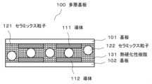
本実施形態では、磁性デバイスで用いられる多層基板について説明する。図1は、本発明の第1の実施形態の多層基板100の断面図の例である。多層基板100は、2層の基板101及び102が、対向する導体111及び112を持つ2層の多層基板である。導体111及び112は、それぞれ、基板101及び基板102の上に形成される。基板101及び102の材料は、例えばガラスエポキシ樹脂である。導体111及び112は、例えば、ぞれぞれ、基板101及び102上に形成された銅のプリント配線である。基板101及び102の両面に導体が配線されていてもよい。導体111及び112は、多層基板100上の導体が巻線体を構成するように、適宜、基板間のスルーホール等で接続される。多層基板を用いて巻線体を構成する基本的な構造は公知であるため、多層基板における巻線体の配線についての説明は省略する。また、巻線体を用いた磁性デバイスの形態の例については第2の実施形態以降で説明する。In this embodiment, a multilayer substrate used in a magnetic device will be described. FIG. 1 is an example of a cross-sectional view of a multilayer substrate 100 according to a first embodiment of the present invention. The multilayer substrate 100 is a two-layer substrate in which two
多層基板100では、基板101と基板102とが積層される際に、粒径が異なる2種類のセラミックス粒子121及び122が添加された熱硬化性樹脂131が接着剤として用いられる。セラミックス粒子121の粒径dはセラミックス粒子122の粒径Dよりも小さい。粒径は、粒子の平均直径である。粒径が小さいセラミックス粒子121は、基板101と基板102との間に充填される熱硬化性樹脂131の流動性と充填性とを大きく損なわないように添加される。粒径dは、例えば1μm以下である。In the multilayer substrate 100, when the
また、セラミックス粒子121よりも粒径が大きいセラミックス粒子122が導体111と導体112との間に充填されることにより、導体111と導体112との間の最小距離が担保される。例えば、粒径Dのセラミックス粒子122を熱硬化性樹脂131に添加することで、導体111と導体112との間にセラミックス粒子122が充填される。従って、セラミックス粒子122を熱硬化性樹脂131に添加することによって、導体111と導体112との間の距離をD以上とすることができる。すなわち、セラミックス粒子122の粒径Dは、導体111と導体112との間の最小間隔が担保されるように設定されてもよい。また、粒径Dは、導体111と導体112との間の絶縁に必要とされる間隔以上であってもよい。粒径Dは、多層基板100における導体111と112の間隔と略一致するように選択されてもよい。粒径Dを大きくすることで、導体111と導体112との間の距離も大きくなり、絶縁性能も向上する。一方、粒径Dが大きくなると基板101と基板102との間の間隔(すなわち、熱硬化性樹脂131の層の厚さ)が大きくなり、多層基板100の熱抵抗が増大する。従って、セラミックス粒子122の粒径Dは、基板間の絶縁性能を担保できる範囲で、小さくすることが好ましい。In addition, the ceramic particles 122, which have a larger particle size than the ceramic particles 121, are filled between the conductors 111 and 112, thereby ensuring the minimum distance between the conductors 111 and 112. For example, by adding ceramic particles 122 with a particle size D to the thermosetting resin 131, the ceramic particles 122 are filled between the conductors 111 and 112. Therefore, by adding the ceramic particles 122 to the thermosetting resin 131, the distance between the conductors 111 and 112 can be made D or more. That is, the particle size D of the ceramic particles 122 may be set so as to ensure the minimum distance between the conductors 111 and 112. In addition, the particle size D may be equal to or greater than the distance required for insulation between the conductors 111 and 112. The particle size D may be selected so as to approximately match the distance between the conductors 111 and 112 in the multilayer substrate 100. By increasing the particle size D, the distance between the conductors 111 and 112 also increases, improving the insulation performance. On the other hand, as the particle size D increases, the gap between the
このように、多層基板100で用いられる熱硬化性樹脂131には、粒径が異なるセラミックス粒子121及び122が添加される。セラミックス粒子121及び122が添加された熱硬化性樹脂131は、絶縁材料の一例である。このような熱硬化性樹脂131を用いて基板を積層することで、粒径の小さいセラミックス粒子121によって熱硬化性樹脂131の流動性及び充填性が確保される。同時に、粒径の大きいセラミックス粒子によって基板間の絶縁距離が確保(すなわち、絶縁性能が担保)される。In this way, ceramic particles 121 and 122 with different particle sizes are added to the thermosetting resin 131 used in the multilayer substrate 100. The thermosetting resin 131 to which the ceramic particles 121 and 122 are added is an example of an insulating material. By stacking substrates using such a thermosetting resin 131, the small particle size ceramic particles 121 ensure the fluidity and filling properties of the thermosetting resin 131. At the same time, the large particle size ceramic particles ensure the insulating distance between the substrates (i.e., the insulating performance is guaranteed).
すなわち、このような構造によれば、粒径の大きいセラミックス粒子121によって基板間の絶縁距離が略均一に確保されるので、多層基板100の製造工程において基板間の離間距離を厳格に調整する工程を省略することができる。換言すれば、多層基板100によれば、製造工程において基板間の位置決めを容易にすることができるので、生産性向上という効果を享受することができる。In other words, with this structure, the large-grain ceramic particles 121 ensure a substantially uniform insulation distance between the substrates, so that the process of strictly adjusting the separation distance between the substrates can be omitted in the manufacturing process of the multilayer substrate 100. In other words, with the multilayer substrate 100, the substrates can be easily positioned in the manufacturing process, which has the effect of improving productivity.
多層基板100の製造時には、セラミックス粒子121及び122の粒径が、熱硬化性樹脂131の流動性及び充填性、並びに多層基板100の絶縁性能に応じて選択される。セラミックス粒子122の添加量は、多層基板100の全体において導体111と導体112との間にセラミックス粒子122が充分に充填される程度であることが好ましい。また、熱硬化性樹脂131の流動性及び充填性を確保するために、熱硬化性樹脂131においてセラミックス粒子121が占める体積又は質量の割合は、セラミックス粒子122が占める体積又は質量の割合よりも大きくてもよい。When manufacturing the multilayer substrate 100, the particle sizes of the ceramic particles 121 and 122 are selected according to the fluidity and filling property of the thermosetting resin 131, and the insulating performance of the multilayer substrate 100. The amount of ceramic particles 122 added is preferably such that the ceramic particles 122 are sufficiently filled between the conductors 111 and 112 throughout the multilayer substrate 100. In addition, in order to ensure the fluidity and filling property of the thermosetting resin 131, the proportion of the volume or mass occupied by the ceramic particles 121 in the thermosetting resin 131 may be greater than the proportion of the volume or mass occupied by the ceramic particles 122.
セラミックス粒子121の添加量を増加させることで、より多くの熱硬化性樹脂131をセラミックス粒子121に置き換えることができる。これによって、多層基板100の熱抵抗をさらに低下させることができるとともに、多層基板100の熱膨張率も低下させることができる。熱抵抗の低下は多層基板100の放熱能力の拡大に寄与する。さらに、多層基板100の熱膨張率の低下によって、多層基板100に搭載される比較的熱膨張率が小さい部品と多層基板100との熱膨張率差を低減できる。例えば、多層基板100を用いた磁性デバイスにセラミックスの一種であるフェライトコアが用いられる場合に、フェライトコアと多層基板100との熱膨張率差が低減される。熱膨張率差の低減により、フェライトコアの搭載時に多層基板100との間隙のマージンを小さくできる。また、フェライトコアと多層基板100との接触部分に加わる温度変化による応力を小さくできる。その結果、温度変化によるこれらの部品間の干渉による悪影響を回避しつつ、多層基板100を用いた磁性デバイスの小型化や信頼性の向上が可能となる。By increasing the amount of ceramic particles 121 added, more thermosetting resin 131 can be replaced with ceramic particles 121. This can further reduce the thermal resistance of multilayer substrate 100 and also reduce the thermal expansion coefficient of multilayer substrate 100. The reduction in thermal resistance contributes to the expansion of heat dissipation capacity of multilayer substrate 100. Furthermore, the reduction in the thermal expansion coefficient of multilayer substrate 100 can reduce the difference in thermal expansion coefficient between the multilayer substrate 100 and the components with relatively small thermal expansion coefficients mounted on multilayer substrate 100. For example, when a ferrite core, which is a type of ceramic, is used in a magnetic device using multilayer substrate 100, the difference in thermal expansion coefficient between the ferrite core and multilayer substrate 100 is reduced. The reduction in the thermal expansion coefficient difference can reduce the margin of the gap between the ferrite core and multilayer substrate 100 when mounting the ferrite core. In addition, the stress due to temperature change applied to the contact portion between the ferrite core and multilayer substrate 100 can be reduced. As a result, it is possible to miniaturize magnetic devices using the multilayer substrate 100 and improve their reliability while avoiding the adverse effects of interference between these components caused by temperature changes.
セラミックス粒子121及び122が添加された熱硬化性樹脂131を用いて基板101と基板102とが接着される。粒径の大きいセラミックス粒子122により、導体111と導体112との距離は、基板101と基板102とを接着するのみで容易かつ確実に制御できる。また、セラミックス粒子122によって、基板間の距離を絶縁に必要な最低限の値とすることができる。その結果、セラミックス粒子121及び122を含む熱硬化性樹脂131が多層基板100の全体に占める体積及び質量の割合も低減され、そして多層基板100の熱抵抗も低減される。例えば、複数の巻線体を含む多層基板100を用いて構成された磁性デバイスは、一部の巻線体のみが磁性デバイスとして動作している場合でも、その巻線体からの熱を多層基板100の全体で効率よく放熱できるため、巻線体の温度上昇を抑制できる。これは、磁性デバイスの信頼性の向上に貢献する。The
(第1の実施形態の他の構成)
熱抵抗が小さいという多層基板100の効果は、以下の要素を備える多層基板によっても実現される。図1の対応する要素の参照符号を括弧内に示す。すなわち、多層基板(100)は、導体(111及び112)が配線された複数の基板(101及び102)と、第1の粒径(D)を持つ第1の絶縁粒子(122)が添加された絶縁材料(131)と、を含む。多層基板(100)は、積層された複数の基板において、それぞれ隣り合う2枚の基板(101及び102)間には、第1の絶縁粒子(122)が、隣り合う2枚の基板に配線された導体(111及び112)とそれぞれ接触するように配置された積層構造をなす。ここで、第1の絶縁粒子(122)は、これらの2枚の基板における導体(111及び112)の間隔に略一致する第1の粒径(D)を持つ。 (Other configurations of the first embodiment)
The effect of the multilayer substrate 100 having a small thermal resistance can also be achieved by a multilayer substrate having the following elements. The reference symbols of the corresponding elements in FIG. 1 are shown in parentheses. That is, the multilayer substrate (100) includes a plurality of substrates (101 and 102) on which conductors (111 and 112) are wired, and an insulating material (131) to which first insulating particles (122) having a first particle size (D) are added. The multilayer substrate (100) has a laminated structure in which the first insulating particles (122) are arranged between two adjacent substrates (101 and 102) in the laminated substrates so as to contact the conductors (111 and 112) wired to the two adjacent substrates. Here, the first insulating particles (122) have a first particle size (D) that is approximately equal to the distance between the conductors (111 and 112) in these two substrates.
このような多層基板は、積層される基板の導体間の間隔に略一致する第1の粒径の絶縁粒子(122)が絶縁材料(131)に添加されているため、基板101と基板102とを積層するのみで、基板(101及び102)の間を所定の間隔で積層できる。このような構成により、絶縁材料の厚さが小さい(すなわち、熱抵抗の低い)多層基板(100)を容易に製造できる。従って、多層基板100に搭載された部品の一部が発熱した場合でも、発熱した部品及びその周辺の局所的な温度上昇を回避できる。In such a multilayer board, insulating particles (122) of a first particle size that approximately matches the spacing between the conductors of the laminated boards are added to the insulating material (131), so that the boards (101 and 102) can be laminated at a predetermined spacing simply by laminating
図2は、上述した他の構成における多層基板の製造方法の例を示すフローチャートである。まず、積層された複数の基板の導体(111、112)の間隔に基づいて、第1の粒径(D)を持つ第1の絶縁粒子(122)が選択される(図2のステップS01)。そして、第1の絶縁粒子(122)が絶縁材料(131)に添加される(ステップS02)。最後に、絶縁材料(131)によって複数の基板(101、102)が積層される。Figure 2 is a flow chart showing an example of a method for manufacturing a multilayer board in the other configuration described above. First, based on the spacing between the conductors (111, 112) of the stacked multiple boards, first insulating particles (122) having a first particle size (D) are selected (step S01 in Figure 2). Then, the first insulating particles (122) are added to an insulating material (131) (step S02). Finally, multiple boards (101, 102) are stacked by the insulating material (131).
(第1の実施形態の変形例)
図3は、多層基板100Aの断面図の例を示す図である。多層基板100Aでは、多層基板100の基板101及び102に加えて基板103及び104が積層されている。基板101と基板102との間、基板102と基板103との間、基板103と基板104との間には、ぞれぞれ、図1で説明したセラミックス粒子121及び122が添加された熱硬化性樹脂131が充填されている。このように、図1の多層基板100の構造は、より層数の多い多層基板100Aにも適用できる。基板を多層化することにより、巻線体の巻数を増加させることができる。多層基板100Aの層数はさらに多くてもよい。 (Modification of the first embodiment)
FIG. 3 is a diagram showing an example of a cross-sectional view of the multilayer substrate 100A. In the multilayer substrate 100A, in addition to the
(第2の実施形態)
本実施形態では、2系統(すなわち、「1+1」)の冗長構成を備える電源装置に用いられる集積型磁性デバイスについて説明する。 Second Embodiment
In this embodiment, an integrated magnetic device used in a power supply unit having a two-system (i.e., "1+1") redundant configuration will be described.
図4は、本実施形態の集積型磁性デバイスが用いられる電源装置800の構成例を示す図である。電源装置800は、2台の電源回路801及び802を備える。電源回路801及び802は、入力された直流電圧Vinを変圧して直流電圧Voutを出力する。例えば、Vin=57V、Vout=12Vである。Voutは、図示されない負荷に供給される。Figure 4 is a diagram showing an example of the configuration of a power supply unit 800 in which the integrated magnetic device of this embodiment is used. The power supply unit 800 includes two power supply circuits 801 and 802. The power supply circuits 801 and 802 transform an input DC voltage Vin and output a DC voltage Vout. For example, Vin = 57 V, Vout = 12 V. Vout is supplied to a load (not shown).
通常は電源回路801及び802は同時に動作する。そして、電源回路801及び802の一方が故障した場合には、他方の電源回路のみが動作する。例えば、電源回路801が故障した場合は、電源回路801は直流電圧Voutの出力を停止し、電源回路802のみが直流電圧Voutを出力する。このように、電源装置800は、2系統の電源回路(電源回路801及び電源回路802)による「1+1」冗長構成を備える。Normally, power supply circuits 801 and 802 operate simultaneously. If one of power supply circuits 801 and 802 fails, only the other power supply circuit operates. For example, if power supply circuit 801 fails, power supply circuit 801 stops outputting DC voltage Vout, and only power supply circuit 802 outputs DC voltage Vout. In this way, power supply device 800 has a "1+1" redundant configuration with two power supply circuits (power supply circuit 801 and power supply circuit 802).
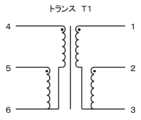
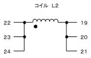
電源回路801は、内部に絶縁トランスT1及び平滑用インダクタL1を1個ずつ備える。電源回路802の構成は電源回路801と同一であり、電源回路802は絶縁トランスT2及び平滑用インダクタL2を1個ずつ備える。以下では、絶縁トランスT1及び絶縁トランスT2をそれぞれトランスT1及びトランスT2と記載する。また、平滑用インダクタL1及び平滑用インダクタL2をそれぞれコイルL1及びコイルL2と記載する。後述する集積型磁性デバイス201は、電源装置800で用いられるトランスT1及びT2、並びに、コイルL1及びL2の4個の磁性デバイスが集積化された電気部品である。図4では、破線で囲まれた4個の磁性デバイスが、1個の集積型磁性デバイス201に含まれる。The power supply circuit 801 includes an insulating transformer T1 and a smoothing inductor L1. The power supply circuit 802 has the same configuration as the power supply circuit 801, and includes an insulating transformer T2 and a smoothing inductor L2. Hereinafter, the insulating transformer T1 and the insulating transformer T2 will be referred to as transformer T1 and transformer T2, respectively. The smoothing inductor L1 and the smoothing inductor L2 will be referred to as coil L1 and coil L2, respectively. The integrated magnetic device 201, which will be described later, is an electrical component that integrates four magnetic devices, namely, the transformers T1 and T2, and the coils L1 and L2, used in the power supply unit 800. In FIG. 4, the four magnetic devices surrounded by dashed lines are included in one integrated magnetic device 201.
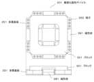
図5-図8は、それぞれ、トランスT1及びT2、並びにコイルL1及びL2の端子配置の例を示す図である。図9は、集積型磁性デバイス201で用いられる多層基板251の上面図の例である。トランスT1及びT2、並びにコイルL1及びL2はいずれも6個の端子を持つ。多層基板251は、これらを集積化するために、図9に示すように、24個の端子252を備える。Figures 5 to 8 are diagrams showing examples of terminal arrangements for transformers T1 and T2, and coils L1 and L2, respectively. Figure 9 is an example of a top view of a multi-layer substrate 251 used in the integrated magnetic device 201. Each of the transformers T1 and T2, and the coils L1 and L2, has six terminals. In order to integrate these, the multi-layer substrate 251 has 24 terminals 252, as shown in Figure 9.
図9を参照すると、1枚の多層基板251には、トランスT1及びT2にそれぞれ対応する巻線体211及び212と、コイルL1及びL2にそれぞれ対応する巻線体213及び214とが形成されている。巻線体211-214は、多層基板251の、楕円形の破線で囲まれた範囲内に形成される。巻線体211-214の中央部には、多層基板251を貫通する長円形の孔253が開けられている。後述するように、これらの4個の孔253に磁性体が挿入されることで、巻線体211-214は独立した磁性デバイス(すなわち、トランス又はコイル)として所定の機能を発揮する。孔253に挿入された磁性体は、それぞれの磁性デバイスの長手方向の磁路として用いられる。Referring to FIG. 9, a single multilayer substrate 251 is formed with
図10は、巻線体211-214と組み合わせて用いられる磁性体281の上面図及び側面図の例である。磁性体281は、巻線体211-214のコアとして用いられる。磁性体281の材料は、例えばフェライトである。磁性体281は、巻線体211-214を表及び裏から挟み込むように、多層基板251に装着される。1個の孔253には、磁性体281の長円形の凸部282が多層基板251の表及び裏から1個ずつ挿入される。Figure 10 shows an example of a top view and a side view of the magnetic body 281 used in combination with the windings 211-214. The magnetic body 281 is used as a core for the windings 211-214. The material of the magnetic body 281 is, for example, ferrite. The magnetic body 281 is attached to the multi-layer board 251 so as to sandwich the windings 211-214 from the front and back. One oval protrusion 282 of the magnetic body 281 is inserted into each
図11は、集積型磁性デバイス201の上面図の例である。多層基板251に4組の磁性体281が装着されることで、多層基板251は集積型磁性デバイス201として機能する。磁性体281と多層基板251との固定手段は特に限定されず、例えば接着剤を用いてもよい。Figure 11 is an example of a top view of the integrated magnetic device 201. By mounting four sets of magnetic bodies 281 on the multi-layer substrate 251, the multi-layer substrate 251 functions as the integrated magnetic device 201. There are no particular limitations on the means for fixing the magnetic bodies 281 to the multi-layer substrate 251, and for example, an adhesive may be used.
多層基板251における基板の積層構造は、第1の実施形態の図1及び図3で例示した多層基板100又は100Aと同様である。すなわち、多層基板251は、粒径の異なるセラミックス粒子121及び122が添加された熱硬化性樹脂131を用いて、紙面に垂直な方向に基板が積層された2層以上の多層基板である。1個の多層基板251には、既知の配線手法により、導体を用いて巻線体211-214が構成されている。多層基板251は、トランスT1及びT2、コイルL1及びL2のそれぞれの仕様に基づいて算出された数の基板を積層して製造される。第1の実施形態の多層基板100及び100Aと同様に、多層基板251に集積された4個の巻線体211-214の間は、低い熱抵抗で結合される。The laminated structure of the substrates in the multilayer substrate 251 is the same as that of the multilayer substrate 100 or 100A illustrated in FIG. 1 and FIG. 3 of the first embodiment. That is, the multilayer substrate 251 is a multilayer substrate of two or more layers in which substrates are laminated in a direction perpendicular to the paper surface using a thermosetting resin 131 to which ceramic particles 121 and 122 with different particle sizes are added. In one multilayer substrate 251, the windings 211-214 are configured using conductors by a known wiring method. The multilayer substrate 251 is manufactured by laminating a number of substrates calculated based on the specifications of the transformers T1 and T2 and the coils L1 and L2. As with the multilayer substrates 100 and 100A of the first embodiment, the four windings 211-214 integrated in the multilayer substrate 251 are connected with low thermal resistance.
24個の端子252は、多層基板251の導体に形成された、巻線体211-214の図示されない端子に接続されている。端子252は、トランスT1及びT2、コイルL1及びL2を電源回路801及び802の回路基板に搭載する際に用いられる端子である。図5-図8の端子1-24が、それぞれ、図9の24個の端子252のいずれか1個に接続されるように、多層基板251の導体の配線が設計される。端子252と電源回路801及び802の回路基板との間の電気的な接続手段は任意であり、例えば両者の間は銅線で配線される。なお、図5-図8の端子1-24をすべて電源回路801及び802と接続する必要はない。電源回路801及び802の機能を実現するために必要とされる端子のみが、端子252を介して電源装置800と接続されてもよい。このように、多層基板251を用いた集積型磁性デバイス201は、2系統の電源回路801及び802で用いられるトランスT1及びT2、並びにコイルL1及びL2の機能を1個の部品で担うことができる。The 24 terminals 252 are connected to terminals (not shown) of the windings 211-214 formed on the conductors of the multilayer substrate 251. The terminals 252 are used when mounting the transformers T1 and T2 and the coils L1 and L2 on the circuit boards of the power supply circuits 801 and 802. The wiring of the conductors of the multilayer substrate 251 is designed so that the terminals 1-24 in Figs. 5-8 are each connected to one of the 24 terminals 252 in Fig. 9. The electrical connection means between the terminals 252 and the circuit boards of the power supply circuits 801 and 802 is arbitrary, and for example, the two are wired with copper wires. It is not necessary to connect all of the terminals 1-24 in Figs. 5-8 to the power supply circuits 801 and 802. Only the terminals required to realize the functions of the power supply circuits 801 and 802 may be connected to the power supply device 800 via the terminals 252. In this way, the integrated magnetic device 201 using the multilayer substrate 251 can perform the functions of the transformers T1 and T2 and the coils L1 and L2 used in the two power supply circuits 801 and 802 in a single component.
電源回路801及び802が正常に動作している場合は、電源回路801及び802はいずれも負荷に直流電圧Voutを供給する。このため、トランスT1及びT2、並びにコイルL1及びL2の全てにおいて電力が消費される。従って、すべての巻線体は、電力損失の発生によって熱源となる。電源回路801及び802の一方が故障等により停止した場合には、稼働を継続する他方の電源回路によって、電源装置800が供給していた電力が負荷へ供給される。この場合、稼働する電源回路のトランス及びコイルは電源回路2台分の電力を扱うことになるため、集積型磁性デバイス201の発熱も稼働する電源回路のトランス及びコイルに集中する。例えば、電源回路801が停止し、電源回路802のみが稼働する場合には、トランスT1及びコイルL1は発熱せず、トランスT2及びコイルL2の発熱量(すなわち、巻線体213及び214の発熱量)は大きく増加する。このような場合でも、集積型磁性デバイス201は、多層基板251の各層の基板が低い熱抵抗で積層されているため、トランスT2及びコイルL2の発熱を多層基板251の全体に効率よく伝搬させ、集積型磁性デバイス201の全体で放熱できる。その結果、電源回路802のみが稼働している場合でもトランスT2及びコイルL2の近傍のみが発熱することを抑制でき、これらの磁性デバイスの局所的な温度上昇を抑制できる。When the power supply circuits 801 and 802 are operating normally, both of them supply a DC voltage Vout to the load. Therefore, power is consumed in all of the transformers T1 and T2 and the coils L1 and L2. Therefore, all of the windings become heat sources due to power loss. When one of the power supply circuits 801 and 802 stops due to a failure or the like, the power supplied by the power supply device 800 is supplied to the load by the other power supply circuit that continues to operate. In this case, the transformer and coil of the operating power supply circuit handle the power of two power supply circuits, so the heat generated by the integrated magnetic device 201 is also concentrated in the transformer and coil of the operating power supply circuit. For example, when the power supply circuit 801 stops and only the power supply circuit 802 operates, the transformer T1 and coil L1 do not generate heat, and the heat generation of the transformer T2 and coil L2 (i.e., the heat generation of the
なお、集積型磁性デバイス201の小型化や磁性デバイス内の熱分布の均一化のためには、巻線体211-214の相互の距離は小さいほどよい。しかし、巻線体同士の距離が小さすぎると、ある巻線体の磁路から漏れた磁束が隣接する他の巻線体の磁路に混入し、それぞれの巻線体の動作に悪影響を及ぼす恐れがある。このような悪影響を回避するためには、隣接する巻線体の磁路が互いに直交するように巻線体を配置することが好ましい。多層基板251においては、隣接する巻線体において、磁性体281によるそれぞれの磁路は直交する。例えば、トランスT1(巻線体211)の磁路と、コイルL1(巻線体212)及びコイルL2(巻線体213)の磁路とは直交する。このような配置により、隣接する磁性デバイスからの漏れ磁束による不要な電力伝搬やノイズの混入を抑制できる。In order to miniaturize the integrated magnetic device 201 and to uniformly distribute heat within the magnetic device, the closer the distance between the windings 211-214, the better. However, if the distance between the windings is too small, the magnetic flux leaking from the magnetic path of one winding may mix with the magnetic path of another adjacent winding, adversely affecting the operation of each winding. In order to avoid such adverse effects, it is preferable to arrange the windings so that the magnetic paths of adjacent windings are orthogonal to each other. In the multilayer board 251, the magnetic paths of the magnetic bodies 281 in adjacent windings are orthogonal to each other. For example, the magnetic path of the transformer T1 (winding 211) is orthogonal to the magnetic paths of the coil L1 (winding 212) and the coil L2 (winding 213). This arrangement can suppress unnecessary power propagation and noise contamination due to leakage flux from adjacent magnetic devices.
以上説明したように、集積型磁性デバイス201には、電源回路801及び802で用いられるトランスT1及びT2(絶縁トランス)、並びにコイルL1及びL2(平滑用インダクタ)が集積されている。そして、集積型磁性デバイス201の多層基板251を構成する基板は、第1の実施形態で説明したように、低い熱抵抗で積層される。このため、集積型磁性デバイス201は、稼働中の電源回路の磁性デバイスから発生した熱を、集積型磁性デバイス201の全体に低い熱抵抗で伝搬させることができる。その結果、集積型磁性デバイス201の内部で発生した熱は集積型磁性デバイス201全体に低い熱抵抗で拡散され、電源回路で使用されている磁性デバイスの局所的な温度上昇を抑制できる。As described above, the integrated magnetic device 201 integrates the transformers T1 and T2 (insulating transformers) and coils L1 and L2 (smoothing inductors) used in the power supply circuits 801 and 802. The substrates constituting the multilayer substrate 251 of the integrated magnetic device 201 are laminated with low thermal resistance as described in the first embodiment. Therefore, the integrated magnetic device 201 can propagate heat generated from the magnetic devices of the power supply circuit during operation throughout the integrated magnetic device 201 with low thermal resistance. As a result, the heat generated inside the integrated magnetic device 201 is diffused throughout the integrated magnetic device 201 with low thermal resistance, and local temperature rises in the magnetic devices used in the power supply circuit can be suppressed.
(第2の実施形態の変形例)
図12は、多層基板251に備えられるブロック301の上面図及び側面図の例である。多層基板251の熱抵抗をさらに低下させるために、多層基板251はブロック301を備えてもよい。ブロック301は略四角形の枠状の金属であり、材質は例えばアルミニウムである。ブロック301は中央部に貫通孔302を持ち、また、磁性体281との接触を回避するための切り欠きを4か所に有する。 (Modification of the second embodiment)
12 is a top view and a side view of an example of a block 301 provided in the multilayer substrate 251. In order to further reduce the thermal resistance of the multilayer substrate 251, the multilayer substrate 251 may be provided with a block 301. The block 301 is a metal frame having a substantially rectangular shape, and is made of, for example, aluminum. The block 301 has a through hole 302 in the center, and also has four notches to avoid contact with the magnetic material 281.
図13はブロック301を備えた集積型磁性デバイス201の底面図及び側面図の例である。ブロック301は、複数の巻線体211-214の間を熱結合させることで、多層基板251の熱抵抗をさらに低下させる。多層基板251とブロック301とは、巻線体211-214の近傍において接合される。多層基板251とブロック301とは例えばメタルコンポジットにより接合されてもよく、他の手段によって接合されてもよい。多層基板251がブロック301を備えることにより、集積型磁性デバイス201に搭載された磁性デバイスの温度上昇をさらに抑制できる。Figure 13 shows an example of a bottom view and a side view of an integrated magnetic device 201 including a block 301. The block 301 further reduces the thermal resistance of the multilayer substrate 251 by thermally coupling the multiple windings 211-214. The multilayer substrate 251 and the block 301 are joined in the vicinity of the windings 211-214. The multilayer substrate 251 and the block 301 may be joined, for example, by a metal composite, or by other means. By including the block 301 in the multilayer substrate 251, the temperature rise of the magnetic device mounted on the integrated magnetic device 201 can be further suppressed.
第2の実施形態及びその変形例では、電源装置800が、電源回路801及び802を備える「1+1」冗長構成である場合について説明した。しかし、集積型磁性デバイス201は、3以上の複数の系統の電源回路で用いられる磁性デバイスを混載してもよい。この場合、1つ以上の系統の電源回路が故障した結果残余の系統の電源回路の磁性デバイスの発熱量が上昇した場合でも、集積型磁性デバイス201は、稼働している系統の磁性デバイスの熱を効率よく放熱できる。In the second embodiment and its modified example, the power supply unit 800 has a "1+1" redundant configuration including power supply circuits 801 and 802. However, the integrated magnetic device 201 may also include magnetic devices used in three or more power supply circuits. In this case, even if one or more power supply circuits fail and the heat generation amount of the magnetic devices in the power supply circuits of the remaining systems increases, the integrated magnetic device 201 can efficiently dissipate the heat of the magnetic devices in the operating systems.
集積型磁性デバイス201に搭載される磁性デバイスはトランス及びコイルに限定されず、また、磁性デバイスの個数も4個に限定されない。さらに、多層基板251が磁性デバイス以外の電子デバイスを搭載した場合でも、多層基板251は熱抵抗が低いため、当該電子デバイスの発熱による当該電子デバイスの温度上昇を抑制できる。The magnetic devices mounted on the integrated magnetic device 201 are not limited to a transformer and a coil, and the number of magnetic devices is not limited to four. Furthermore, even if the multilayer substrate 251 is mounted with an electronic device other than a magnetic device, the multilayer substrate 251 has low thermal resistance, so that the temperature rise of the electronic device due to heat generation of the electronic device can be suppressed.
(第3の実施形態)
図14は、本発明の第3の実施形態の集積型磁性デバイス830の構成例を示す図である。図14は、集積型磁性デバイス830の上面図の例及び上面図のA-A’断面図の例を示す。集積型磁性デバイス830は、1個の多層基板810と2組の磁性体820とを備える。多層基板810は2個の巻線体811及び812を備える。巻線体811及び812は、それぞれ、多層基板810の各層に形成された導体によって形成される。巻線体811及び812は、それぞれ、磁性体820と組み合わされることで、独立した磁性デバイスとして動作する。磁性デバイスは、例えば、トランス又はコイルであるが、これらには限定されない。磁性体820として、巻線体811及び812のそれぞれに、図10に示した磁性体281が2個ずつ用いられてもよい。 Third Embodiment
FIG. 14 is a diagram showing a configuration example of an integrated magnetic device 830 according to a third embodiment of the present invention. FIG. 14 shows an example of a top view of the integrated magnetic device 830 and an example of an A-A' cross-sectional view of the top view. The integrated magnetic device 830 includes one multilayer substrate 810 and two sets of magnetic bodies 820. The multilayer substrate 810 includes two winding
多層基板810の積層方法は図1又は図3に例示した多層基板100又は100Aと同様であり、絶縁材料を用いて複数の基板を積層することで製造される。絶縁材料は、例えば、多層基板810の基板間における、巻線体を構成する導体の間隔に基づいて選択された粒径の絶縁粒子が添加された樹脂である。The method of laminating the multilayer board 810 is the same as that of the multilayer board 100 or 100A illustrated in FIG. 1 or FIG. 3, and the multilayer board 810 is manufactured by laminating multiple boards using an insulating material. The insulating material is, for example, a resin to which insulating particles of a particle size selected based on the spacing between the conductors that make up the winding body between the boards of the multilayer board 810 are added.
このような構成を備える集積型磁性デバイス830は、1枚の多層基板810に複数の磁性デバイスを集積している。また、多層基板810を構成する複数の基板は、巻線体を構成する導体の間隔に基づいて選択された粒径の絶縁粒子が添加された樹脂を用いて積層される。このような樹脂を用いることで熱抵抗が低く絶縁性能が高い多層基板を容易に製造できる。そして、集積型磁性デバイス830は、発生する熱を集積型磁性デバイス830の全体で発散できる。従って、集積型磁性デバイス830は、複数の磁性デバイスのいずれかが動作していない場合でも、動作中の磁性デバイスの温度上昇を抑制できる。The integrated magnetic device 830 having such a configuration integrates multiple magnetic devices on one multilayer substrate 810. The multiple substrates that make up the multilayer substrate 810 are laminated using a resin to which insulating particles with a particle size selected based on the spacing between the conductors that make up the winding body are added. By using such a resin, a multilayer substrate with low thermal resistance and high insulation performance can be easily manufactured. The integrated magnetic device 830 can dissipate the generated heat throughout the entire integrated magnetic device 830. Therefore, the integrated magnetic device 830 can suppress the temperature rise of the magnetic device during operation even when any of the multiple magnetic devices is not operating.
以上、実施形態を参照して本願発明を説明したが、本願発明は上記の実施形態に限定されない。本願発明の構成や詳細には、本願発明のスコープ内で当業者が理解し得る様々な変更をすることができる。例えば、各実施形態で例示された多層基板及び集積型磁性デバイスは、電源回路のほか、冗長性を備えた送信機、受信機、コンピュータシステムなどで用いられてもよい。また、各基板の導体は巻線体でなくとも、各実施形態の構成によって、導体からの熱を効率的に放熱できる。Although the present invention has been described above with reference to the embodiments, the present invention is not limited to the above embodiments. Various modifications that can be understood by those skilled in the art can be made to the configuration and details of the present invention within the scope of the present invention. For example, the multilayer substrate and integrated magnetic device exemplified in each embodiment may be used in a power supply circuit, as well as a transmitter, receiver, computer system, etc. with redundancy. Furthermore, even if the conductor of each substrate is not a winding body, the configuration of each embodiment allows efficient dissipation of heat from the conductor.
また、それぞれの実施形態に記載された構成は、必ずしも互いに排他的なものではない。本発明の作用及び効果は、上述の実施形態の全部又は一部を組み合わせた構成によって実現されてもよい。Furthermore, the configurations described in each embodiment are not necessarily mutually exclusive. The actions and effects of the present invention may be achieved by a configuration that combines all or part of the above-described embodiments.
100、100A、251、810 多層基板
101-104 基板
111-112 導体
121-122 セラミックス粒子
131 熱硬化性樹脂
201、830 集積型磁性デバイス
211-214 巻線体
252 端子
253 孔
281、820 磁性体
282 凸部
301 ブロック
302 貫通孔
800 電源装置
801、802 電源回路
811-812 巻線体
900 多層基板
901、902 基板
911、912 導体
921 ガラス繊維
931 熱硬化性樹脂 100, 100A, 251, 810 Multilayer substrate 101-104 Substrate 111-112 Conductor 121-122 Ceramic particles 131 Thermosetting resin 201, 830 Integrated magnetic device 211-214 Winding body 252
Claims (10)
Translated fromJapanese第1の粒径を持つ第1の絶縁粒子と、
前記第1の粒径よりも小さい第2の粒径を持つ第2の絶縁粒子が熱硬化性樹脂に添加された絶縁材料と、
を含み、
積層された前記複数の基板において、それぞれ隣り合う2枚の基板間には、該2枚の基板における前記導体の間隔に略一致する前記第1の粒径を持つ第1の絶縁粒子が、該隣り合う2枚の基板に配線された導体とそれぞれ接触するように配置された積層構造をなし、
前記熱硬化性樹脂の流動性及び充填性を確保するため前記第2の絶縁粒子が占める体積の割合が前記第1の絶縁粒子が占める体積の割合よりも高い、又は、前記第2の絶縁粒子が占める質量の割合が前記第1の絶縁粒子が占める質量の割合よりも高い、
多層基板。 A plurality of substrates on which conductors are wired;
first insulating particles having a first particle size;
an insulating material in which second insulating particles having a second particle size smaller than the first particle size are added to a thermosetting resin;
Including,
In the plurality of laminated substrates, a laminate structure is formed in which first insulating particles having the first particle size approximately equal to the distance between the conductors in the two substratesare disposed between each two adjacent substrates so as to contact the conductors wired to the two adjacent substrates,
In order to ensure the fluidity and filling property of the thermosetting resin, a volume ratio occupied by the second insulating particles is higher than a volume ratio occupied by the first insulating particles, or a mass ratio occupied by the second insulating particles is higher than a mass ratio occupied by the first insulating particles.
Multilayer board.
前記複数の巻線体のそれぞれが独立した複数の磁性デバイスを構成するように配置された磁性体と、
を備える、集積型磁性デバイス。 A multilayer substrate according to claim4 including a plurality of the winding bodies;
a magnetic body arranged so that each of the plurality of winding bodies constitutes a plurality of independent magnetic devices;
An integrated magnetic device comprising:
前記電源装置は請求項5又は6に記載された集積型磁性デバイスを備え、
前記磁性デバイスは、隣接する前記巻線体の磁路が互いに直交するように前記巻線体が配置され、
前記複数の磁性デバイスの1つは前記第1の系統で用いられ、
前記複数の磁性デバイスの他の1つは前記第2の系統で用いられる、
電源装置。 A power supply device having a redundant configuration consisting of a first system and a second system,
The power supply device comprises the integrated magnetic device according to claim5 or 6 ,
The magnetic device has windings arranged such that magnetic paths of adjacent windings are perpendicular to each other,
one of the plurality of magnetic devices is used in the first system;
Another of the plurality of magnetic devices is used in the second system.
Power supply.
積層された前記複数の基板の前記導体の間隔に基づいて第1の粒径を持つ第1の絶縁粒子を選択し、
前記第1の絶縁粒子を、前記第1の粒径よりも小さい第2の粒径を持つ第2の絶縁粒子が熱硬化性樹脂に添加された絶縁材料に添加し、
前記絶縁材料によって前記複数の基板を積層する、
多層基板の製造方法であって、
前記熱硬化性樹脂の流動性及び充填性を確保するため前記第2の絶縁粒子が占める体積の割合が前記第1の絶縁粒子が占める体積の割合よりも高い、又は、前記第2の絶縁粒子が占める質量の割合が前記第1の絶縁粒子が占める質量の割合よりも高い、
多層基板の製造方法。 A method for manufacturing a multilayer substrate including a plurality of substrates on which conductors are wired, comprising the steps of:
selecting first insulating particles having a first particle size based on the spacing between the conductors of the plurality of stacked substrates;
adding the first insulating particles to an insulating materialin which second insulating particles having a second particle size smaller than the first particle size are added to a thermosetting resin ;
Stacking the plurality of substrates with the insulating material;
A method for manufacturing a multilayer substrate, comprising the steps of:
In order to ensure the fluidity and filling property of the thermosetting resin, a volume ratio occupied by the second insulating particles is higher than a volume ratio occupied by the first insulating particles, or a mass ratio occupied by the second insulating particles is higher than a mass ratio occupied by the first insulating particles.
A method for manufacturing a multilayer board .
前記第1の粒径を持つ第1の絶縁粒子が添加された前記絶縁材料を介して前記隣り合う2枚の基板を複数積層することによって、前記多層基板を構成する、
請求項8に記載された多層基板の製造方法。 the first insulating particles have the first particle size that is approximately equal to a distance between the conductors between two adjacent substrates among the plurality of substrates that are stacked;
forming the multilayer substrate by stacking two adjacent substrates via the insulating material to which the first insulating particles having the first particle size have been added;
A method for manufacturing a multilayer substrate according to claim8 .
Priority Applications (5)
| Application Number | Priority Date | Filing Date | Title |
|---|---|---|---|
| JP2021045546AJP7534243B2 (en) | 2021-03-19 | 2021-03-19 | Multilayer substrate, integrated magnetic device, power supply device, and method of manufacturing multilayer substrate |
| US18/282,023US20240038442A1 (en) | 2021-03-19 | 2022-02-22 | Multilayer substrate, integrated magnetic device, power source apparatus, and multilayer substrate production method |
| EP22771024.1AEP4276857A4 (en) | 2021-03-19 | 2022-02-22 | Multilayer substrate, integrated magnetic device, power source device, and method for producing a multilayer substrate |
| PCT/JP2022/007283WO2022196265A1 (en) | 2021-03-19 | 2022-02-22 | Multilayer substrate, integrated magnetic device, power source apparatus, and multilayer substrate production method |
| JP2024032133AJP7667400B2 (en) | 2021-03-19 | 2024-03-04 | Power Supplies |
Applications Claiming Priority (1)
| Application Number | Priority Date | Filing Date | Title |
|---|---|---|---|
| JP2021045546AJP7534243B2 (en) | 2021-03-19 | 2021-03-19 | Multilayer substrate, integrated magnetic device, power supply device, and method of manufacturing multilayer substrate |
Related Child Applications (1)
| Application Number | Title | Priority Date | Filing Date |
|---|---|---|---|
| JP2024032133ADivisionJP7667400B2 (en) | 2021-03-19 | 2024-03-04 | Power Supplies |
Publications (2)
| Publication Number | Publication Date |
|---|---|
| JP2022144502A JP2022144502A (en) | 2022-10-03 |
| JP7534243B2true JP7534243B2 (en) | 2024-08-14 |
Family
ID=83322265
Family Applications (2)
| Application Number | Title | Priority Date | Filing Date |
|---|---|---|---|
| JP2021045546AActiveJP7534243B2 (en) | 2021-03-19 | 2021-03-19 | Multilayer substrate, integrated magnetic device, power supply device, and method of manufacturing multilayer substrate |
| JP2024032133AActiveJP7667400B2 (en) | 2021-03-19 | 2024-03-04 | Power Supplies |
Family Applications After (1)
| Application Number | Title | Priority Date | Filing Date |
|---|---|---|---|
| JP2024032133AActiveJP7667400B2 (en) | 2021-03-19 | 2024-03-04 | Power Supplies |
Country Status (4)
| Country | Link |
|---|---|
| US (1) | US20240038442A1 (en) |
| EP (1) | EP4276857A4 (en) |
| JP (2) | JP7534243B2 (en) |
| WO (1) | WO2022196265A1 (en) |
Citations (6)
| Publication number | Priority date | Publication date | Assignee | Title |
|---|---|---|---|---|
| JP2000515680A (en) | 1996-01-05 | 2000-11-21 | アライドシグナル・インコーポレーテッド | Printed circuit multilayer assembly and method of manufacturing the same |
| JP2001160510A (en) | 1999-12-01 | 2001-06-12 | Tdk Corp | Coil device |
| JP2002530900A (en) | 1998-11-19 | 2002-09-17 | アライドシグナル インコーポレイテッド | Printed circuit assembly with locally enhanced wiring density |
| JP2006324642A (en) | 2005-04-19 | 2006-11-30 | Renesas Technology Corp | Semiconductor device and manufacturing method thereof |
| JP2008308576A (en) | 2007-06-14 | 2008-12-25 | Mitsubishi Electric Corp | Method for producing thermally conductive resin sheet, thermally conductive resin sheet, and power module using the same |
| WO2017126357A1 (en) | 2016-01-21 | 2017-07-27 | 三菱電機株式会社 | Circuit device and electric power converter |
Family Cites Families (18)
| Publication number | Priority date | Publication date | Assignee | Title |
|---|---|---|---|---|
| JPH04174980A (en)* | 1990-11-07 | 1992-06-23 | Hitachi Chem Co Ltd | Connecting member for circuit |
| JPH1140425A (en)* | 1997-07-16 | 1999-02-12 | Murata Mfg Co Ltd | Transformers and inductors |
| JP2000260639A (en) | 1999-03-11 | 2000-09-22 | Murata Mfg Co Ltd | Coil device and switching power supply device |
| JP2001053441A (en) | 1999-08-06 | 2001-02-23 | Canon Components Inc | Manufacture of multilayer wiring board and insulating interlayer joining material |
| SE0004125L (en) | 2000-11-10 | 2002-05-11 | Ericsson Telefon Ab L M | Spacer holding dielectric layer |
| JP2004040025A (en) | 2002-07-08 | 2004-02-05 | Natl Space Development Agency Of Japan | Sheet type transformer and electronic equipment |
| JP2007180105A (en)* | 2005-12-27 | 2007-07-12 | Sanyo Electric Co Ltd | Circuit board and circuit device using the same, and manufacturing method thereof |
| JP2008066529A (en)* | 2006-09-07 | 2008-03-21 | Fuji Electric Systems Co Ltd | Multi-stage AC reactor core coil structure and auxiliary power unit having the core coil structure |
| JP4825286B2 (en)* | 2009-08-07 | 2011-11-30 | ナミックス株式会社 | Manufacturing method of multilayer wiring board |
| JP6116806B2 (en)* | 2012-02-27 | 2017-04-19 | 新電元工業株式会社 | Thin core coil and thin transformer |
| JP2013207115A (en)* | 2012-03-28 | 2013-10-07 | Dexerials Corp | Connection structure and manufacturing method of the same, electronic component and manufacturing method of the same, connection method of electronic component |
| JP6066865B2 (en)* | 2013-08-15 | 2017-01-25 | 信越化学工業株式会社 | High dielectric constant epoxy resin composition and semiconductor device |
| JP2016123191A (en) | 2014-12-25 | 2016-07-07 | キヤノン株式会社 | Wiring structure of sheet type transformer and mounting method thereof |
| WO2017208332A1 (en) | 2016-05-31 | 2017-12-07 | 新電元工業株式会社 | Coil structure and magnetic component |
| JP6783308B2 (en) | 2016-06-24 | 2020-11-11 | 三菱電機株式会社 | Insulated converter |
| JP7160576B2 (en)* | 2017-06-26 | 2022-10-25 | 積水化学工業株式会社 | Laminate manufacturing method |
| US20200258675A1 (en) | 2019-02-08 | 2020-08-13 | Lear Corporation | Hybrid transformer for dc/dc converter |
| GB2589960B (en) | 2019-09-16 | 2023-09-20 | Nextremity Solutions Inc | Bone cut guide apparatus |
- 2021
- 2021-03-19JPJP2021045546Apatent/JP7534243B2/enactiveActive
- 2022
- 2022-02-22WOPCT/JP2022/007283patent/WO2022196265A1/ennot_activeCeased
- 2022-02-22USUS18/282,023patent/US20240038442A1/enactivePending
- 2022-02-22EPEP22771024.1Apatent/EP4276857A4/enactivePending
- 2024
- 2024-03-04JPJP2024032133Apatent/JP7667400B2/enactiveActive
Patent Citations (6)
| Publication number | Priority date | Publication date | Assignee | Title |
|---|---|---|---|---|
| JP2000515680A (en) | 1996-01-05 | 2000-11-21 | アライドシグナル・インコーポレーテッド | Printed circuit multilayer assembly and method of manufacturing the same |
| JP2002530900A (en) | 1998-11-19 | 2002-09-17 | アライドシグナル インコーポレイテッド | Printed circuit assembly with locally enhanced wiring density |
| JP2001160510A (en) | 1999-12-01 | 2001-06-12 | Tdk Corp | Coil device |
| JP2006324642A (en) | 2005-04-19 | 2006-11-30 | Renesas Technology Corp | Semiconductor device and manufacturing method thereof |
| JP2008308576A (en) | 2007-06-14 | 2008-12-25 | Mitsubishi Electric Corp | Method for producing thermally conductive resin sheet, thermally conductive resin sheet, and power module using the same |
| WO2017126357A1 (en) | 2016-01-21 | 2017-07-27 | 三菱電機株式会社 | Circuit device and electric power converter |
Also Published As
| Publication number | Publication date |
|---|---|
| JP2024060624A (en) | 2024-05-02 |
| EP4276857A1 (en) | 2023-11-15 |
| US20240038442A1 (en) | 2024-02-01 |
| JP2022144502A (en) | 2022-10-03 |
| WO2022196265A1 (en) | 2022-09-22 |
| JP7667400B2 (en) | 2025-04-23 |
| EP4276857A4 (en) | 2025-03-12 |
Similar Documents
| Publication | Publication Date | Title |
|---|---|---|
| US6420953B1 (en) | Multi-layer, multi-functioning printed circuit board | |
| JP6170568B2 (en) | Planar transformer | |
| CN102844825B (en) | Devices that make up planar transformers and busbars | |
| CN107683513B (en) | Planar Transformers for Energy Transfer | |
| CN107534424B (en) | Noise filter | |
| US8406007B1 (en) | Magnetic circuit board connector component | |
| JP7667400B2 (en) | Power Supplies | |
| JP5311462B2 (en) | Multi-layer substrate transformer | |
| JP2008205350A (en) | Magnetic device | |
| JPH11329851A (en) | Coil device | |
| US11075029B2 (en) | Coil module | |
| JP7443780B2 (en) | Multilayer board circuit structure | |
| JP2004349400A (en) | Thermal conductive circuit board and power module using the same | |
| JP3095350B2 (en) | Sheet coil laminated type transformer and its terminal structure | |
| JP2005080382A (en) | Power conversion module device and power supply device using the same | |
| US20020163818A1 (en) | Magnetic device and method of manufacture therefor | |
| JP4674545B2 (en) | Electromagnetic induction parts and power supply | |
| JPH10189355A (en) | Printed circuit board for laminated transformer and power supply unit | |
| KR20080004870U (en) | High Efficiency Standalone Planar Transformer | |
| JP7632151B2 (en) | Electronics | |
| JP2021019014A (en) | Coil component and transformer | |
| JP4802616B2 (en) | LC composite parts | |
| JP5544180B2 (en) | Transformer module and electronic device | |
| CN117524667A (en) | Power module and electronic equipment | |
| WO2018123961A1 (en) | Multilayered wiring board and method for manufacturing multilayered wiring board |
Legal Events
| Date | Code | Title | Description |
|---|---|---|---|
| RD01 | Notification of change of attorney | Free format text:JAPANESE INTERMEDIATE CODE: A7421 Effective date:20211111 | |
| A621 | Written request for application examination | Free format text:JAPANESE INTERMEDIATE CODE: A621 Effective date:20220715 | |
| A131 | Notification of reasons for refusal | Free format text:JAPANESE INTERMEDIATE CODE: A131 Effective date:20230718 | |
| A521 | Request for written amendment filed | Free format text:JAPANESE INTERMEDIATE CODE: A523 Effective date:20230915 | |
| A02 | Decision of refusal | Free format text:JAPANESE INTERMEDIATE CODE: A02 Effective date:20231205 | |
| A61 | First payment of annual fees (during grant procedure) | Free format text:JAPANESE INTERMEDIATE CODE: A61 Effective date:20240801 | |
| R150 | Certificate of patent or registration of utility model | Ref document number:7534243 Country of ref document:JP Free format text:JAPANESE INTERMEDIATE CODE: R150 |