JP7532423B2 - Display Panel and Electronic Device - Google Patents
Display Panel and Electronic DeviceDownload PDFInfo
- Publication number
- JP7532423B2 JP7532423B2JP2021577077AJP2021577077AJP7532423B2JP 7532423 B2JP7532423 B2JP 7532423B2JP 2021577077 AJP2021577077 AJP 2021577077AJP 2021577077 AJP2021577077 AJP 2021577077AJP 7532423 B2JP7532423 B2JP 7532423B2
- Authority
- JP
- Japan
- Prior art keywords
- base substrate
- anode
- driving circuit
- orthogonal projection
- via hole
- Prior art date
- Legal status (The legal status is an assumption and is not a legal conclusion. Google has not performed a legal analysis and makes no representation as to the accuracy of the status listed.)
- Active
Links
Images


Classifications
- G—PHYSICS
- G09—EDUCATION; CRYPTOGRAPHY; DISPLAY; ADVERTISING; SEALS
- G09G—ARRANGEMENTS OR CIRCUITS FOR CONTROL OF INDICATING DEVICES USING STATIC MEANS TO PRESENT VARIABLE INFORMATION
- G09G3/00—Control arrangements or circuits, of interest only in connection with visual indicators other than cathode-ray tubes
- G09G3/20—Control arrangements or circuits, of interest only in connection with visual indicators other than cathode-ray tubes for presentation of an assembly of a number of characters, e.g. a page, by composing the assembly by combination of individual elements arranged in a matrix no fixed position being assigned to or needed to be assigned to the individual characters or partial characters
- G09G3/22—Control arrangements or circuits, of interest only in connection with visual indicators other than cathode-ray tubes for presentation of an assembly of a number of characters, e.g. a page, by composing the assembly by combination of individual elements arranged in a matrix no fixed position being assigned to or needed to be assigned to the individual characters or partial characters using controlled light sources
- G09G3/30—Control arrangements or circuits, of interest only in connection with visual indicators other than cathode-ray tubes for presentation of an assembly of a number of characters, e.g. a page, by composing the assembly by combination of individual elements arranged in a matrix no fixed position being assigned to or needed to be assigned to the individual characters or partial characters using controlled light sources using electroluminescent panels
- G09G3/32—Control arrangements or circuits, of interest only in connection with visual indicators other than cathode-ray tubes for presentation of an assembly of a number of characters, e.g. a page, by composing the assembly by combination of individual elements arranged in a matrix no fixed position being assigned to or needed to be assigned to the individual characters or partial characters using controlled light sources using electroluminescent panels semiconductive, e.g. using light-emitting diodes [LED]
- G09G3/3208—Control arrangements or circuits, of interest only in connection with visual indicators other than cathode-ray tubes for presentation of an assembly of a number of characters, e.g. a page, by composing the assembly by combination of individual elements arranged in a matrix no fixed position being assigned to or needed to be assigned to the individual characters or partial characters using controlled light sources using electroluminescent panels semiconductive, e.g. using light-emitting diodes [LED] organic, e.g. using organic light-emitting diodes [OLED]
- G09G3/3225—Control arrangements or circuits, of interest only in connection with visual indicators other than cathode-ray tubes for presentation of an assembly of a number of characters, e.g. a page, by composing the assembly by combination of individual elements arranged in a matrix no fixed position being assigned to or needed to be assigned to the individual characters or partial characters using controlled light sources using electroluminescent panels semiconductive, e.g. using light-emitting diodes [LED] organic, e.g. using organic light-emitting diodes [OLED] using an active matrix
- G09G3/3233—Control arrangements or circuits, of interest only in connection with visual indicators other than cathode-ray tubes for presentation of an assembly of a number of characters, e.g. a page, by composing the assembly by combination of individual elements arranged in a matrix no fixed position being assigned to or needed to be assigned to the individual characters or partial characters using controlled light sources using electroluminescent panels semiconductive, e.g. using light-emitting diodes [LED] organic, e.g. using organic light-emitting diodes [OLED] using an active matrix with pixel circuitry controlling the current through the light-emitting element
- G—PHYSICS
- G09—EDUCATION; CRYPTOGRAPHY; DISPLAY; ADVERTISING; SEALS
- G09G—ARRANGEMENTS OR CIRCUITS FOR CONTROL OF INDICATING DEVICES USING STATIC MEANS TO PRESENT VARIABLE INFORMATION
- G09G3/00—Control arrangements or circuits, of interest only in connection with visual indicators other than cathode-ray tubes
- G09G3/20—Control arrangements or circuits, of interest only in connection with visual indicators other than cathode-ray tubes for presentation of an assembly of a number of characters, e.g. a page, by composing the assembly by combination of individual elements arranged in a matrix no fixed position being assigned to or needed to be assigned to the individual characters or partial characters
- G09G3/22—Control arrangements or circuits, of interest only in connection with visual indicators other than cathode-ray tubes for presentation of an assembly of a number of characters, e.g. a page, by composing the assembly by combination of individual elements arranged in a matrix no fixed position being assigned to or needed to be assigned to the individual characters or partial characters using controlled light sources
- G09G3/30—Control arrangements or circuits, of interest only in connection with visual indicators other than cathode-ray tubes for presentation of an assembly of a number of characters, e.g. a page, by composing the assembly by combination of individual elements arranged in a matrix no fixed position being assigned to or needed to be assigned to the individual characters or partial characters using controlled light sources using electroluminescent panels
- G09G3/32—Control arrangements or circuits, of interest only in connection with visual indicators other than cathode-ray tubes for presentation of an assembly of a number of characters, e.g. a page, by composing the assembly by combination of individual elements arranged in a matrix no fixed position being assigned to or needed to be assigned to the individual characters or partial characters using controlled light sources using electroluminescent panels semiconductive, e.g. using light-emitting diodes [LED]
- G09G3/3208—Control arrangements or circuits, of interest only in connection with visual indicators other than cathode-ray tubes for presentation of an assembly of a number of characters, e.g. a page, by composing the assembly by combination of individual elements arranged in a matrix no fixed position being assigned to or needed to be assigned to the individual characters or partial characters using controlled light sources using electroluminescent panels semiconductive, e.g. using light-emitting diodes [LED] organic, e.g. using organic light-emitting diodes [OLED]
- G09G3/3225—Control arrangements or circuits, of interest only in connection with visual indicators other than cathode-ray tubes for presentation of an assembly of a number of characters, e.g. a page, by composing the assembly by combination of individual elements arranged in a matrix no fixed position being assigned to or needed to be assigned to the individual characters or partial characters using controlled light sources using electroluminescent panels semiconductive, e.g. using light-emitting diodes [LED] organic, e.g. using organic light-emitting diodes [OLED] using an active matrix
- H—ELECTRICITY
- H10—SEMICONDUCTOR DEVICES; ELECTRIC SOLID-STATE DEVICES NOT OTHERWISE PROVIDED FOR
- H10K—ORGANIC ELECTRIC SOLID-STATE DEVICES
- H10K59/00—Integrated devices, or assemblies of multiple devices, comprising at least one organic light-emitting element covered by group H10K50/00
- H10K59/10—OLED displays
- H10K59/12—Active-matrix OLED [AMOLED] displays
- H10K59/121—Active-matrix OLED [AMOLED] displays characterised by the geometry or disposition of pixel elements
- H10K59/1213—Active-matrix OLED [AMOLED] displays characterised by the geometry or disposition of pixel elements the pixel elements being TFTs
- H—ELECTRICITY
- H10—SEMICONDUCTOR DEVICES; ELECTRIC SOLID-STATE DEVICES NOT OTHERWISE PROVIDED FOR
- H10K—ORGANIC ELECTRIC SOLID-STATE DEVICES
- H10K59/00—Integrated devices, or assemblies of multiple devices, comprising at least one organic light-emitting element covered by group H10K50/00
- H10K59/10—OLED displays
- H10K59/12—Active-matrix OLED [AMOLED] displays
- H10K59/121—Active-matrix OLED [AMOLED] displays characterised by the geometry or disposition of pixel elements
- H10K59/1216—Active-matrix OLED [AMOLED] displays characterised by the geometry or disposition of pixel elements the pixel elements being capacitors
- H—ELECTRICITY
- H10—SEMICONDUCTOR DEVICES; ELECTRIC SOLID-STATE DEVICES NOT OTHERWISE PROVIDED FOR
- H10K—ORGANIC ELECTRIC SOLID-STATE DEVICES
- H10K59/00—Integrated devices, or assemblies of multiple devices, comprising at least one organic light-emitting element covered by group H10K50/00
- H10K59/80—Constructional details
- H10K59/805—Electrodes
- H10K59/8051—Anodes
- G—PHYSICS
- G09—EDUCATION; CRYPTOGRAPHY; DISPLAY; ADVERTISING; SEALS
- G09G—ARRANGEMENTS OR CIRCUITS FOR CONTROL OF INDICATING DEVICES USING STATIC MEANS TO PRESENT VARIABLE INFORMATION
- G09G2300/00—Aspects of the constitution of display devices
- G09G2300/04—Structural and physical details of display devices
- G09G2300/0421—Structural details of the set of electrodes
- G09G2300/0426—Layout of electrodes and connections
- G—PHYSICS
- G09—EDUCATION; CRYPTOGRAPHY; DISPLAY; ADVERTISING; SEALS
- G09G—ARRANGEMENTS OR CIRCUITS FOR CONTROL OF INDICATING DEVICES USING STATIC MEANS TO PRESENT VARIABLE INFORMATION
- G09G2300/00—Aspects of the constitution of display devices
- G09G2300/08—Active matrix structure, i.e. with use of active elements, inclusive of non-linear two terminal elements, in the pixels together with light emitting or modulating elements
- G09G2300/0809—Several active elements per pixel in active matrix panels
- G09G2300/0842—Several active elements per pixel in active matrix panels forming a memory circuit, e.g. a dynamic memory with one capacitor
- G—PHYSICS
- G09—EDUCATION; CRYPTOGRAPHY; DISPLAY; ADVERTISING; SEALS
- G09G—ARRANGEMENTS OR CIRCUITS FOR CONTROL OF INDICATING DEVICES USING STATIC MEANS TO PRESENT VARIABLE INFORMATION
- G09G2320/00—Control of display operating conditions
- G09G2320/02—Improving the quality of display appearance
- G09G2320/029—Improving the quality of display appearance by monitoring one or more pixels in the display panel, e.g. by monitoring a fixed reference pixel
- G09G2320/0295—Improving the quality of display appearance by monitoring one or more pixels in the display panel, e.g. by monitoring a fixed reference pixel by monitoring each display pixel
- G—PHYSICS
- G09—EDUCATION; CRYPTOGRAPHY; DISPLAY; ADVERTISING; SEALS
- G09G—ARRANGEMENTS OR CIRCUITS FOR CONTROL OF INDICATING DEVICES USING STATIC MEANS TO PRESENT VARIABLE INFORMATION
- G09G2330/00—Aspects of power supply; Aspects of display protection and defect management
- G09G2330/12—Test circuits or failure detection circuits included in a display system, as permanent part thereof
- H—ELECTRICITY
- H10—SEMICONDUCTOR DEVICES; ELECTRIC SOLID-STATE DEVICES NOT OTHERWISE PROVIDED FOR
- H10D—INORGANIC ELECTRIC SEMICONDUCTOR DEVICES
- H10D86/00—Integrated devices formed in or on insulating or conducting substrates, e.g. formed in silicon-on-insulator [SOI] substrates or on stainless steel or glass substrates
- H10D86/40—Integrated devices formed in or on insulating or conducting substrates, e.g. formed in silicon-on-insulator [SOI] substrates or on stainless steel or glass substrates characterised by multiple TFTs
- H10D86/60—Integrated devices formed in or on insulating or conducting substrates, e.g. formed in silicon-on-insulator [SOI] substrates or on stainless steel or glass substrates characterised by multiple TFTs wherein the TFTs are in active matrices
Landscapes
- Engineering & Computer Science (AREA)
- Physics & Mathematics (AREA)
- Geometry (AREA)
- Microelectronics & Electronic Packaging (AREA)
- Computer Hardware Design (AREA)
- General Physics & Mathematics (AREA)
- Theoretical Computer Science (AREA)
- Electroluminescent Light Sources (AREA)
- Devices For Indicating Variable Information By Combining Individual Elements (AREA)
- Control Of Indicators Other Than Cathode Ray Tubes (AREA)
- Control Of El Displays (AREA)
Description
Translated fromJapanese本開示は、表示技術の技術分野に関し、特に、表示パネル及び電子装置に関する。The present disclosure relates to the technical field of display technology, and in particular to display panels and electronic devices.
透明表示は、全く新しい表示技術として、観察者が表示スクリーを透過してスクリーンの後方の背景を見ることができ、その新しい表示効果はディスプレイの応用分野を広げ、広く注目されている。Transparent display is a completely new display technology that allows the viewer to see through the display screen and into the background behind it. This new display effect has expanded the application fields of displays and has attracted widespread attention.
本開示のいくつかの実施例は、表示パネルを提供し、ベース基板と、前記ベース基板に設けられた画素と、を含み、前記画素は、第1のサブ画素と第2のサブ画素とを有し、前記第1のサブ画素は、第1のサブ画素駆動回路と、前記第1のサブ画素駆動回路によって駆動される第1の発光素子とを有し、前記第2のサブ画素は、第2のサブ画素駆動回路と、前記第2のサブ画素駆動回路によって駆動される第2の発光素子とを有し、前記第1のサブ画素駆動回路および前記第2のサブ画素駆動回路は、ベース基板に平行な第1の方向に順次に配列され、ベース基板に平行で第1の方向に交差する第2の方向にそれぞれ延在し、前記第1の発光素子は、前記第1のサブ画素駆動回路に電気的に接続された第1のアノードを有し、前記第2の発光素子は、前記第2のサブ画素駆動回路に電気的に接続された第2のアノードを有し、前記第1のアノード及び前記第2のアノードのそれぞれの前記ベース基板での正投影は、前記第1のサブ画素駆動回路の前記ベース基板での正投影と、前記第2のサブ画素駆動回路の前記ベース基板での正投影とを部分的に覆い、前記第1のアノードの前記ベース基板での正投影と、前記第2のアノードの前記ベース基板での正投影とは重ならない。Some embodiments of the present disclosure provide a display panel, comprising: a base substrate; and a pixel disposed on the base substrate, the pixel having a first subpixel and a second subpixel, the first subpixel having a first subpixel driving circuit and a first light-emitting element driven by the first subpixel driving circuit, the second subpixel having a second subpixel driving circuit and a second light-emitting element driven by the second subpixel driving circuit, the first subpixel driving circuit and the second subpixel driving circuit being sequentially arranged in a first direction parallel to the base substrate, and being intersecting with the first direction parallel to the base substrate. The first light-emitting element has a first anode electrically connected to the first subpixel driving circuit, and the second light-emitting element has a second anode electrically connected to the second subpixel driving circuit, and the orthogonal projections of the first anode and the second anode on the base substrate partially cover the orthogonal projections of the first subpixel driving circuit on the base substrate and the orthogonal projections of the second subpixel driving circuit on the base substrate, and do not overlap with the orthogonal projections of the first anode on the base substrate and the orthogonal projections of the second anode on the base substrate.
いくつかの実施例において、前記第1のサブ画素駆動回路および第2のサブ画素駆動回路は、検出トランジスタと、蓄積容量と、スイッチングトランジスタとを有し、前記第2の方向において、前記検出トランジスタおよび前記スイッチングトランジスタは、前記蓄積容量の両側にそれぞれ配置され、前記第1のアノードおよび前記第2のアノードのうちの一方の前記ベース基板での正投影は、前記第1のサブ画素駆動回路における検出トランジスタの前記ベース基板での正投影を少なくとも部分的に覆い、かつ前記第2のサブ画素駆動回路における検出トランジスタの前記ベース基板での正投影を少なくとも部分的に覆い、前記第1のアノードおよび前記第2のアノードのうちの他方の前記ベース基板での正投影は、前記第1のサブ画素駆動回路におけるスイッチングトランジスタの前記ベース基板での正投影を少なくとも部分的に覆い、かつ前記第2のサブ画素駆動回路におけるスイッチングトランジスタの前記ベース基板での正投影を少なくとも部分的に覆う。In some embodiments, the first subpixel drive circuit and the second subpixel drive circuit have a detection transistor, a storage capacitance, and a switching transistor, and in the second direction, the detection transistor and the switching transistor are respectively arranged on both sides of the storage capacitance, and an orthogonal projection of one of the first anode and the second anode on the base substrate at least partially covers an orthogonal projection of the detection transistor in the first subpixel drive circuit on the base substrate and at least partially covers an orthogonal projection of the detection transistor in the second subpixel drive circuit on the base substrate, and an orthogonal projection of the other of the first anode and the second anode on the base substrate at least partially covers an orthogonal projection of the switching transistor in the first subpixel drive circuit on the base substrate and at least partially covers an orthogonal projection of the switching transistor in the second subpixel drive circuit on the base substrate.
いくつかの実施例において、前記第1のアノードおよび前記第2のアノードのうちの前記一方の前記ベース基板での正投影は、前記第1のサブ画素駆動回路における蓄積容量の第1の部分の前記ベース基板での正投影を覆い、かつ前記第2のサブ画素駆動回路における蓄積容量の第1の部分の前記ベース基板での正投影を覆い、前記第1のアノードおよび前記第2のアノードのうちの前記他方の前記ベース基板での正投影は、前記第1のサブ画素駆動回路における蓄積容量の第2の部分の前記ベース基板での正投影を覆い、且つ前記第2のサブ画素駆動回路における蓄積容量の第2の部分の前記ベース基板での正投影を覆い、前記第1のサブ画素駆動回路および前記第2のサブ画素駆動回路のそれぞれにおいて、前記蓄積容量の第1の部分は、前記蓄積容量の第2の部分よりも前記検出トランジスタに近い。In some embodiments, the orthogonal projection of one of the first anode and the second anode on the base substrate covers the orthogonal projection of the first portion of the storage capacitance in the first subpixel driving circuit on the base substrate and covers the orthogonal projection of the first portion of the storage capacitance in the second subpixel driving circuit on the base substrate, the orthogonal projection of the other of the first anode and the second anode on the base substrate covers the orthogonal projection of the second portion of the storage capacitance in the first subpixel driving circuit on the base substrate and covers the orthogonal projection of the second portion of the storage capacitance in the second subpixel driving circuit on the base substrate, and in each of the first subpixel driving circuit and the second subpixel driving circuit, the first portion of the storage capacitance is closer to the detection transistor than the second portion of the storage capacitance.
いくつかの実施例において、前記第1のアノードおよび前記第2のアノードのうちの前記一方の前記ベース基板での正投影は、前記第1のサブ画素駆動回路における検出トランジスタの前記ベース基板での正投影を完全に覆い、かつ前記第2のサブ画素駆動回路における検出トランジスタの前記ベース基板での正投影を完全に覆い、前記第1のアノードおよび前記第2のアノードのうちの前記他方の前記ベース基板での正投影は、前記第1のサブ画素駆動回路におけるスイッチングトランジスタの前記ベース基板での正投影を完全に覆い、且つ前記第2のサブ画素駆動回路における前記スイッチングトランジスタの前記ベース基板での正投影を完全に覆う。In some embodiments, the orthogonal projection of one of the first anode and the second anode on the base substrate completely covers the orthogonal projection of the detection transistor in the first subpixel drive circuit on the base substrate and completely covers the orthogonal projection of the detection transistor in the second subpixel drive circuit on the base substrate, and the orthogonal projection of the other of the first anode and the second anode on the base substrate completely covers the orthogonal projection of the switching transistor in the first subpixel drive circuit on the base substrate and completely covers the orthogonal projection of the switching transistor in the second subpixel drive circuit on the base substrate.
いくつかの実施例において、前記画素は、第3のサブ画素と第4のサブ画素とを更に有し、前記第3のサブ画素は、第3のサブ画素駆動回路と、前記第3のサブ画素駆動回路によって駆動される第3の発光素子とを有し、前記第4のサブ画素は、第4のサブ画素駆動回路と、前記第4のサブ画素駆動回路によって駆動される第4の発光素子とを有し、前記第1のサブ画素駆動回路、前記第2のサブ画素駆動回路、前記第3のサブ画素駆動回路及び前記第4のサブ画素駆動回路は、ベース基板に平行な第1の方向に沿って順次に配列され、前記第2の方向に沿ってそれぞれ延在し、
前記第3の発光素子は、前記第3のサブ画素駆動回路に電気的に接続された第3のアノードを有し、前記第4の発光素子は、前記第4のサブ画素駆動回路に電気的に接続された第4のアノードを有し、前記第3のアノードおよび前記第4のアノードのそれぞれの前記ベース基板での正投影は、いずれも前記第3のサブ画素駆動回路の前記ベース基板での正投影と、前記第4のサブ画素駆動回路の前記ベース基板での正投影とを部分的に覆い、前記第1のアノード、前記第2のアノード、前記第3のアノードおよび前記第4のアノードの前記ベース基板での正投影は、いずれも重ならない。 In some embodiments, the pixel further comprises a third sub-pixel and a fourth sub-pixel, the third sub-pixel comprising a third sub-pixel driving circuit and a third light-emitting element driven by the third sub-pixel driving circuit, the fourth sub-pixel comprising a fourth sub-pixel driving circuit and a fourth light-emitting element driven by the fourth sub-pixel driving circuit, the first sub-pixel driving circuit, the second sub-pixel driving circuit, the third sub-pixel driving circuit and the fourth sub-pixel driving circuit being sequentially arranged along a first direction parallel to a base substrate and extending respectively along the second direction;
The third light-emitting element has a third anode electrically connected to the third subpixel driving circuit, and the fourth light-emitting element has a fourth anode electrically connected to the fourth subpixel driving circuit, wherein orthogonal projections of the third anode and the fourth anode on the base substrate both partially cover orthogonal projections of the third subpixel driving circuit on the base substrate and orthogonal projections of the fourth subpixel driving circuit on the base substrate, and orthogonal projections of the first anode, the second anode, the third anode, and the fourth anode on the base substrate do not overlap with each other.
いくつかの実施例において、前記第3のサブ画素駆動回路および前記第4のサブ画素駆動回路は、検出トランジスタ、蓄積容量、スイッチングトランジスタをそれぞれ有し、前記第2の方向において、前記第3のサブ画素駆動回路および前記第4のサブ画素駆動回路の各サブ画素駆動回路において、前記検出トランジスタおよび前記スイッチングトランジスタは、前記蓄積容量の両側にそれぞれ配置され、前記第3のアノードおよび前記第4のアノードの一方の前記ベース基板での正投影は、前記第3のサブ画素駆動回路内の検出トランジスタの前記ベース基板での正投影を少なくとも部分的に覆い、かつ第4のサブ画素駆動回路内の検出トランジスタの前記ベース基板での正投影を少なくとも部分的に覆い、前記第3のアノードおよび前記第4のアノードの他方の前記ベース基板での正投影は、第3のサブ画素駆動回路におけるスイッチングトランジスタの前記ベース基板での正投影を少なくとも部分的に覆い、かつ第4のサブ画素駆動回路におけるスイッチングトランジスタの前記ベース基板での正投影を少なくとも部分的に覆う。In some embodiments, the third subpixel drive circuit and the fourth subpixel drive circuit each have a detection transistor, a storage capacitor, and a switching transistor, and in the second direction, in each subpixel drive circuit of the third subpixel drive circuit and the fourth subpixel drive circuit, the detection transistor and the switching transistor are respectively arranged on both sides of the storage capacitor, and an orthogonal projection of one of the third anode and the fourth anode on the base substrate at least partially covers an orthogonal projection of the detection transistor in the third subpixel drive circuit on the base substrate and at least partially covers an orthogonal projection of the detection transistor in the fourth subpixel drive circuit on the base substrate, and an orthogonal projection of the other of the third anode and the fourth anode on the base substrate at least partially covers an orthogonal projection of the switching transistor in the third subpixel drive circuit on the base substrate and at least partially covers an orthogonal projection of the switching transistor in the fourth subpixel drive circuit on the base substrate.
いくつかの実施例において、前記第3のアノードおよび前記第4のアノードの前記一方の前記ベース基板での正投影は、前記第3のサブ画素駆動回路における蓄積容量の第1の部分の前記ベース基板での正投影を覆い、且つ前記第4のサブ画素駆動回路における蓄積容量の第1の部分の前記ベース基板での正投影を覆い、前記第3のアノードおよび前記第4のアノードの前記他方の前記ベース基板での正投影は、前記第3のサブ画素駆動回路における蓄積容量の第2の部分の前記ベース基板での正投影を覆い、且つ前記第4のサブ画素駆動回路における蓄積容量の第2の部分の前記ベース基板での正投影を覆い、前記第3のサブ画素駆動回路および前記第4のサブ画素駆動回路のそれぞれにおいて、前記蓄積容量の第1の部分は、前記蓄積容量の第2の部分よりも前記検出トランジスタに近い。In some embodiments, the orthogonal projection of one of the third anode and the fourth anode on the base substrate covers the orthogonal projection of the first portion of the storage capacitance in the third subpixel driving circuit on the base substrate and covers the orthogonal projection of the first portion of the storage capacitance in the fourth subpixel driving circuit on the base substrate, the orthogonal projection of the other of the third anode and the fourth anode on the base substrate covers the orthogonal projection of the second portion of the storage capacitance in the third subpixel driving circuit on the base substrate and covers the orthogonal projection of the second portion of the storage capacitance in the fourth subpixel driving circuit on the base substrate, and in each of the third subpixel driving circuit and the fourth subpixel driving circuit, the first portion of the storage capacitance is closer to the detection transistor than the second portion of the storage capacitance.
いくつかの実施例において、前記第3のアノードと前記第4のアノードの前記一方の前記ベース基板での正投影は、前記第3のサブ画素駆動回路における検出トランジスタの前記ベース基板での正投影を完全に覆い、かつ前記第4のサブ画素駆動回路における検出トランジスタの前記ベース基板での正投影を完全に覆い、前記第3のアノードと前記第4のアノードの前記他方の前記ベース基板での正投影は、前記第3のサブ画素駆動回路におけるスイッチングトランジスタの前記ベース基板での正投影を完全に覆い、且つ前記第4のサブ画素駆動回路におけるスイッチングトランジスタの前記ベース基板での正投影を完全に覆う。In some embodiments, the orthogonal projection of one of the third anode and the fourth anode on the base substrate completely covers the orthogonal projection of the detection transistor in the third subpixel drive circuit on the base substrate and completely covers the orthogonal projection of the detection transistor in the fourth subpixel drive circuit on the base substrate, and the orthogonal projection of the other of the third anode and the fourth anode on the base substrate completely covers the orthogonal projection of the switching transistor in the third subpixel drive circuit on the base substrate and completely covers the orthogonal projection of the switching transistor in the fourth subpixel drive circuit on the base substrate.
いくつかの実施例において、前記第1のサブ画素駆動回路、前記第2のサブ画素駆動回路、前記第3のサブ画素駆動回路および前記第4のサブ画素駆動回路は、それぞれ、前記蓄積容量の前記検出トランジスタから遠い側に位置し、前記蓄積容量と前記スイッチングトランジスタとの間に位置する駆動トランジスタをさらに含み、前記駆動トランジスタは、前記第2の方向に前記蓄積容量から順に遠くなるソース、ゲートおよびドレインを有し、前記検出トランジスタは、前記第2の方向に前記蓄積容量から順に遠くなって配置されたソース、ゲートおよびドレインを有し、前記蓄積容量は、前記ベース基板に順に積層された第1の容量電極、第2の容量電極および第3の容量電極を有し、前記駆動トランジスタのソース、前記第3の容量電極および前記検出トランジスタのソースは、同一層に配置され、一体構造に互いに接続されている。In some embodiments, the first subpixel driving circuit, the second subpixel driving circuit, the third subpixel driving circuit and the fourth subpixel driving circuit each further include a driving transistor located on the side of the storage capacitance farther from the detection transistor and between the storage capacitance and the switching transistor, the driving transistor has a source, a gate and a drain arranged in order from the storage capacitance in the second direction, the detection transistor has a source, a gate and a drain arranged in order from the storage capacitance in the second direction, the storage capacitance has a first capacitance electrode, a second capacitance electrode and a third capacitance electrode stacked in order on the base substrate, and the source of the driving transistor, the third capacitance electrode and the source of the detection transistor are arranged in the same layer and are connected to each other in an integral structure.
いくつかの実施例において、前記表示パネルは、各サブ画素駆動回路における前記一体構造を有するソース/ドレイン金属層と、ソース/ドレイン金属層の前記ベース基板から遠い側に位置し、第1のアノード、第2のアノード、第3のアノードおよび第4のアノードを含むアノード層と、前記ソース/ドレイン金属層の前記ベース基板から遠い側に設けられ、かつ、前記アノード層の前記ベース基板に面する側に設けられた平坦化層と、をさらに含み、前記平坦化層には、前記第1のアノードが第1のアノードビアホールによって第1のサブ画素駆動回路の前記一体構造に電気的に接続される第1のアノードビアホールと、前記第2のアノードが第2のアノードビアホールによって第2のサブ画素駆動回路の前記一体構造に電気的に接続される第2のアノードビアホールと、前記第3のアノードが第3のアノードビアホールによって第3のサブ画素駆動回路の前記一体構造に電気的に接続される第3のアノードビアホールと、前記第4のアノードが第4のアノードビアホールによって第4のサブ画素駆動回路の前記一体構造に電気的に接続される第4のアノードビアホールと、が設けられている。In some embodiments, the display panel further includes a source/drain metal layer having the integrated structure in each subpixel driving circuit, an anode layer located on a side of the source/drain metal layer far from the base substrate and including a first anode, a second anode, a third anode and a fourth anode, and a planarization layer provided on the side of the source/drain metal layer far from the base substrate and on a side of the anode layer facing the base substrate, the planarization layer including a first anode connected to the first subpixel driving circuit by a first anode via hole. A first anode via hole electrically connected to the integrated structure of the second subpixel driving circuit, a second anode via hole electrically connecting the second anode to the integrated structure of the second subpixel driving circuit through the second anode via hole, a third anode via hole electrically connecting the third anode to the integrated structure of the third subpixel driving circuit through the third anode via hole, and a fourth anode via hole electrically connecting the fourth anode to the integrated structure of the fourth subpixel driving circuit through the fourth anode via hole.
いくつかの実施例において、前記第1のアノードビアホール及び前記第2のアノードビアホールのうちの1方のアノードビアホールの前記ベース基板での正投影は、前記1つのアノードビアホールに電気的に接続されたサブ画素駆動回路における検出トランジスタのソースの前記ベース基板での正投影内に落ち込み、前記第1のアノードビアホール及び前記第2のアノードビアホールの他方のアノードビアホールの前記ベース基板での正投影は、前記他方のアノードビアホールに電気的に接続されたサブ画素駆動回路における蓄積容量の第3の容量電極の前記ベース基板での正投影内に落ち込み、前記第2の方向において、前記他方のアノードビアホールに電気的に接続されたサブ画素駆動回路における検出トランジスタのソースのベース基板での正投影と、前記他方のアノードビアホールに電気的に接続されたサブ画素駆動回路における駆動トランジスタのソースの前記ベース基板での正投影との間にあり、前記第3のアノードビアホール及び前記第4のアノードビアホールのうちの1方のアノードビアホールの前記ベース基板での正投影は、前記1方のアノードビアホールに電気的に接続されたサブ画素駆動回路における検出トランジスタのソースの前記ベース基板での正投影内に落ち込み、前記第3のアノードビアホール及び前記第4のアノードビアホールの他方のアノードビアホールの前記ベース基板での正投影は、前記他方のアノードビアホールに電気的に接続されたサブ画素駆動回路における蓄積容量の第3の容量電極の前記ベース基板での正投影内に落ち込み、前記第2の方向において、前記他方のアノードビアホールに電気的に接続されたサブ画素駆動回路における検出トランジスタのソースの前記ベース基板での正投影と、前記他方のアノードビアホールに電気的に接続されたサブ画素駆動回路における駆動トランジスタのソースの前記ベース基板での正投影との間にある。In some embodiments, an orthogonal projection on the base substrate of one of the first anode via hole and the second anode via hole falls within an orthogonal projection on the base substrate of a source of a detection transistor in a subpixel driving circuit electrically connected to the one anode via hole, an orthogonal projection on the base substrate of the other of the first anode via hole and the second anode via hole falls within an orthogonal projection on the base substrate of a third capacitance electrode of a storage capacitance in a subpixel driving circuit electrically connected to the other anode via hole, and in the second direction, an orthogonal projection on the base substrate of a source of a detection transistor in a subpixel driving circuit electrically connected to the other anode via hole and an orthogonal projection on the base substrate of a source of a driving transistor in a subpixel driving circuit electrically connected to the other anode via hole are formed. The orthogonal projection on the base substrate of one of the third anode via hole and the fourth anode via hole falls within the orthogonal projection on the base substrate of the source of the detection transistor in the subpixel driving circuit electrically connected to the one anode via hole, and the orthogonal projection on the base substrate of the other anode via hole of the third anode via hole and the fourth anode via hole falls within the orthogonal projection on the base substrate of the third capacitance electrode of the storage capacitance in the subpixel driving circuit electrically connected to the other anode via hole, and in the second direction, it is between the orthogonal projection on the base substrate of the source of the detection transistor in the subpixel driving circuit electrically connected to the other anode via hole and the orthogonal projection on the base substrate of the source of the driving transistor in the subpixel driving circuit electrically connected to the other anode via hole.
いくつかの実施例において、前記第1のアノードビアホールの前記ベース基板での正投影の中心と、前記第3のアノードビアホール及び前記第4のアノードビアホールの一方の前記ベース基板での正投影の中心との直線接続線は、前記第1の方向に沿って延在し、前記第2のアノードビアホールの前記ベース基板での正投影の中心と、前記第3のアノードビアホール及び前記第4のアノードビアホールの他方の前記ベース基板での正投影の中心との直線接続線は、前記第1の方向に沿って延在する。In some embodiments, a straight line connecting the center of the orthogonal projection of the first anode via hole on the base substrate and the center of the orthogonal projection of one of the third anode via hole and the fourth anode via hole on the base substrate extends along the first direction, and a straight line connecting the center of the orthogonal projection of the second anode via hole on the base substrate and the center of the orthogonal projection of the other of the third anode via hole and the fourth anode via hole on the base substrate extends along the first direction.
いくつかの実施例において、前記第1のアノードビアホールの前記ベース基板での正投影は、前記第1のサブ画素駆動回路における検出トランジスタのソースの前記ベース基板での正投影内に落ち込み、前記第2のアノードビアホールの前記ベース基板での正投影は、前記第2のサブ画素駆動回路における蓄積容量の第3の容量電極の前記ベース基板での正投影内に落ち込み、前記第2の方向において、前記第2のサブ画素駆動回路における検出トランジスタのソースの前記ベース基板での正投影と、前記第2のサブ画素駆動回路における駆動トランジスタのソースの前記ベース基板での正投影との間にあり、前記第3のアノードビアホールの前記ベース基板での正投影は、前記第3のサブ画素駆動回路における蓄積容量の第3の容量電極の前記ベース基板での正投影内に落ち込み、前記第2の方向において、前記第3のサブ画素駆動回路における検出トランジスタのソースの前記ベース基板での正投影と、前記第3のサブ画素駆動回路における駆動トランジスタのソースの前記ベース基板での正投影との間にあり、前記第4のアノードビアホールの前記ベース基板での正投影は、前記第4のサブ画素駆動回路における検出トランジスタのソースの前記ベース基板での正投影内に落ち込む。In some embodiments, an orthogonal projection of the first anode via hole on the base substrate falls within an orthogonal projection of a source of a detection transistor in the first subpixel driving circuit on the base substrate, an orthogonal projection of the second anode via hole on the base substrate falls within an orthogonal projection of a third capacitance electrode of a storage capacitance in the second subpixel driving circuit on the base substrate, and in the second direction, an orthogonal projection of a source of a detection transistor in the second subpixel driving circuit on the base substrate and an orthogonal projection of a source of a driving transistor in the second subpixel driving circuit on the base substrate. between the third anode via hole and the third capacitance electrode of the storage capacitance in the third subpixel driving circuit, and between the orthogonal projection on the base substrate of the source of the detection transistor in the third subpixel driving circuit and the orthogonal projection on the base substrate of the source of the driving transistor in the third subpixel driving circuit in the second direction, and the orthogonal projection on the base substrate of the fourth anode via hole and the fourth subpixel driving circuit.
いくつかの実施例において、各サブ画素駆動回路は、容量ビアホールをさらに有し、前記蓄積容量の第3の容量電極は、前記容量ビアホールによって前記第1の容量電極に電気的に接続される。In some embodiments, each subpixel driving circuit further includes a capacitive via hole, and the third capacitive electrode of the storage capacitor is electrically connected to the first capacitive electrode by the capacitive via hole.
いくつかの実施例において、前記第1のサブ画素駆動回路において、前記容量ビアホールは、前記第1のアノードビアホールの前記蓄積容量に近い側に位置し、前記第1のアノードビアホールと前記蓄積容量との間に位置し、前記容量ビアホールの前記ベース基板での正投影の中心と前記第1のアノードビアホールの前記ベース基板での正投影の中心との直線接続線は、第2の方向に延在し、前記容量ビアホールの前記ベース基板での正投影と前記第1のアノードビアホールの前記ベース基板での正投影はいずれも前記第1のアノードの前記ベース基板での正投影内に落ち込み、前記第2のサブ画素駆動回路において、前記容量ビアホールは、前記第2のアノードビアホールの前記検出トランジスタに近い側に位置し、前記容量ビアホールの前記ベース基板での正投影の中心と前記第2のアノードビアホールの前記ベース基板での正投影の中心との直線接続線は、前記第2の方向に延在し、前記容量ビアホールの前記ベース基板での正投影と前記第2のアノードビアホールの前記ベース基板での正投影はいずれも前記第2のアノードの前記ベース基板での正投影内に落ち込み、前記第3のサブ画素駆動回路において、前記容量ビアホールは、前記第3のアノードビアホールの前記検出トランジスタに近い側に位置し、前記容量ビアホールの前記ベース基板での正投影の中心と前記第3のアノードビアホールの前記ベース基板での正投影の中心との直線接続線は、前記第2の方向に延在し、前記容量ビアホールの前記ベース基板での正投影と前記第3のアノードビアホールの前記ベース基板での正投影はいずれも前記第3のアノードの前記ベース基板での正投影内に落ち込み、前記第4のサブ画素駆動回路において、前記容量ビアホールは、前記第4のアノードビアホールの蓄積容量に近い側に位置し、前記第4のアノードビアホールと前記蓄積容量との間に位置し、前記容量ビアホールの前記ベース基板での正投影の中心と前記第4のアノードビアホールの前記ベース基板での正投影の中心との直線接続線は、前記第2の方向に延在し、前記容量ビアホールの前記ベース基板での正投影と前記第4のアノードビアホールの前記ベース基板での正投影はいずれも前記第4のアノードの前記ベース基板での正投影内に落ち込む。In some embodiments, in the first subpixel driving circuit, the capacitive via hole is located on a side of the first anode via hole closer to the storage capacitance, and is located between the first anode via hole and the storage capacitance, a straight line connecting the center of the orthogonal projection of the capacitive via hole on the base substrate and the center of the orthogonal projection of the first anode via hole on the base substrate extends in a second direction, and both the orthogonal projection of the capacitive via hole on the base substrate and the orthogonal projection of the first anode via hole on the base substrate are aligned in a direction parallel to the first anode via hole. a first subpixel driving circuit including a first anode via hole and a second anode via hole, the ... second subpixel driving circuit including a first anode via hole and a second anode via hole, the first subpixel driving circuit including a first anode via hole and a second anode via hole, the second subpixel driving circuit including a first anode via hole and a second anode via hole, the second subpixel driving circuit including a first anode via hole and a second anode via hole, the second subpixel driving circuit including a first anode via hole and a second anode via hole, the second subpixel driving circuit including a first anode via hole and a second anode via hole, the second subpixel driving circuit including a first anode via hole and a second anode via hole, the second subpixel driving circuit including a first anode via hole and a second anode via hole, the second subpixel driving circuit including a first anode via hole and a second anode via hole, the second subpixel driving circuit including a first anode via hole and a second anode via hole, the second subpixel driving circuit including in the third subpixel driving circuit, the capacitive via hole is located on a side of the third anode via hole closer to the detection transistor, a straight line connecting a center of an orthogonal projection of the capacitive via hole on the base substrate and a center of an orthogonal projection of the third anode via hole on the base substrate extends in the second direction, and both the orthogonal projection of the capacitive via hole on the base substrate and the orthogonal projection of the third anode via hole on the base substrate fall within the orthogonal projection of the third anode on the base substrate, In the drive circuit, the capacitive via hole is located on the side closer to the storage capacitance of the fourth anode via hole, and is located between the fourth anode via hole and the storage capacitance, a straight line connecting the center of the orthogonal projection of the capacitive via hole on the base substrate and the center of the orthogonal projection of the fourth anode via hole on the base substrate extends in the second direction, and both the orthogonal projection of the capacitive via hole on the base substrate and the orthogonal projection of the fourth anode via hole on the base substrate fall within the orthogonal projection of the fourth anode on the base substrate.
いくつかの実施例において、各サブ画素駆動回路は、ソースビアホールをさらに有し、各サブ画素駆動回路の検出トランジスタは、アクティブ層をさらに有し、前記検出トランジスタのソースは前記ソースビアホールによってアクティブ層に接続され、前記第1のサブ画素駆動回路のソースビアホールの前記ベース基板での正投影は、前記第1のアノードビアホールの前記ベース基板での正投影内に落ち込み、前記第4のサブ画素駆動回路の前記ソースビアホールの前記ベース基板での正投影は、前記第4のアノードビアホールの前記ベース基板での正投影内に落ち込む。In some embodiments, each subpixel driving circuit further includes a source via hole, the detection transistor of each subpixel driving circuit further includes an active layer, the source of the detection transistor is connected to the active layer by the source via hole, the orthogonal projection of the source via hole of the first subpixel driving circuit on the base substrate falls within the orthogonal projection of the first anode via hole on the base substrate, and the orthogonal projection of the source via hole of the fourth subpixel driving circuit on the base substrate falls within the orthogonal projection of the fourth anode via hole on the base substrate.
いくつかの実施例において、前記表示パネルは、画素定義層をさらに含み、画素定義層は、前記第1の発光素子の発光材料層を収容するための第1の開口と、前記第2の発光素子の発光材料層を収容するための第2の開口と、前記第3の発光素子の発光材料層を収容するための第3の開口と、前記第4の発光素子の発光材料層を収容するための第4の開口と、を有し、前記第1の開口の前記ベース基板での正投影は、前記第1のアノードの前記ベース基板での正投影内に落ち込み、前記第2の開口の前記ベース基板での正投影は、前記第2のアノードの前記ベース基板での正投影内に落ち込み、前記第3の開口の前記ベース基板での正投影は、前記第3のアノードの前記ベース基板での正投影内に落ち込み、前記第4の開口の前記ベース基板での正投影は、前記第4のアノードの前記ベース基板での正投影内に落ち込む。In some embodiments, the display panel further includes a pixel definition layer, the pixel definition layer having a first opening for accommodating the light emitting material layer of the first light emitting element, a second opening for accommodating the light emitting material layer of the second light emitting element, a third opening for accommodating the light emitting material layer of the third light emitting element, and a fourth opening for accommodating the light emitting material layer of the fourth light emitting element, wherein an orthogonal projection of the first opening on the base substrate falls within an orthogonal projection of the first anode on the base substrate, an orthogonal projection of the second opening on the base substrate falls within an orthogonal projection of the second anode on the base substrate, an orthogonal projection of the third opening on the base substrate falls within an orthogonal projection of the third anode on the base substrate, and an orthogonal projection of the fourth opening on the base substrate falls within an orthogonal projection of the fourth anode on the base substrate.
いくつかの実施例において、前記第1の開口の前記ベース基板での正投影は、前記第1のアノードビアホールの前記ベース基板での正投影と重ならず、前記第1の開口の前記ベース基板での正投影は、前記第1のサブ画素駆動回路の容量ビアホールの前記ベース基板での正投影と重ならず、前記第2の開口の前記ベース基板での正投影は、前記第2のアノードビアホールの前記ベース基板での正投影と重ならず、前記第2の開口の前記ベース基板での正投影は、前記第2のサブ画素駆動回路の容量ビアホールの前記ベース基板での正投影と重ならず、前記第3の開口の前記ベース基板での正投影は、前記第3のアノードビアホールの前記ベース基板での正投影と重ならず、前記第3の開口の前記ベース基板での正投影は、前記第3のサブ画素駆動回路の容量ビアホールの前記ベース基板での正投影と重ならず、前記第4の開口の前記ベース基板での正投影は、前記第4のアノードビアホールの前記ベース基板での正投影と重ならず、前記第4の開口の前記ベース基板での正投影は、前記第4のサブ画素駆動回路の容量ビアホールの前記ベース基板での正投影と重ならない。In some embodiments, an orthogonal projection of the first opening on the base substrate does not overlap with an orthogonal projection of the first anode via hole on the base substrate, an orthogonal projection of the first opening on the base substrate does not overlap with an orthogonal projection of the capacitive via hole of the first subpixel driving circuit on the base substrate, an orthogonal projection of the second opening on the base substrate does not overlap with an orthogonal projection of the second anode via hole on the base substrate, and an orthogonal projection of the second opening on the base substrate does not overlap with an orthogonal projection of the capacitive via hole of the second subpixel driving circuit on the base substrate. the orthogonal projection of the third opening on the base substrate does not overlap with the orthogonal projection of the third anode via hole on the base substrate, the orthogonal projection of the third opening on the base substrate does not overlap with the orthogonal projection of the capacitive via hole of the third subpixel driving circuit on the base substrate, the orthogonal projection of the fourth opening on the base substrate does not overlap with the orthogonal projection of the fourth anode via hole on the base substrate, and the orthogonal projection of the fourth opening on the base substrate does not overlap with the orthogonal projection of the capacitive via hole of the fourth subpixel driving circuit on the base substrate.
いくつかの実施例において、前記第1のアノード、前記第2のアノード、前記第3のアノード、及び前記第4のアノードは、2×2行列状に配列され、前記第1のアノードと前記第2のアノードは、前記第2の方向に並んで配置され、前記第3のアノードと前記第4のアノードは、前記第2の方向に並んで配置される。In some embodiments, the first anode, the second anode, the third anode, and the fourth anode are arranged in a 2×2 matrix, the first anode and the second anode are arranged side by side in the second direction, and the third anode and the fourth anode are arranged side by side in the second direction.
いくつかの実施例において、前記画素は、第1の方向に並んで配置された光透過領域と表示領域とを有し、前記第1のサブ画素、前記第2のサブ画素、前記第3のサブ画素および前記第4のサブ画素は、前記表示領域に位置している。In some embodiments, the pixel has a light-transmitting region and a display region arranged side by side in a first direction, and the first subpixel, the second subpixel, the third subpixel and the fourth subpixel are located in the display region.
いくつかの実施例において、前記第2の方向は、前記第1の方向と直交する。In some embodiments, the second direction is perpendicular to the first direction.
いくつかの実施例において、前記表示パネルは、OLED表示パネルである。
本開示のいくつかの実施例は、前記実施例に記載の表示パネルを含む電子装置を提供している。 In some embodiments, the display panel is an OLED display panel.
Some embodiments of the present disclosure provide an electronic device including the display panel according to the embodiments.
本開示の他の特徴、目的、及び利点は、以下の図面を参照してなされる非限定的な実施例の詳細な説明を読むことにより、より明らかとなるであろう。Other features, objects, and advantages of the present disclosure will become more apparent from a detailed description of the non-limiting embodiments that follow, taken in conjunction with the drawings in which:
以下、図面および実施例を参照しながら、本開示をさらに詳細に説明する。本明細書に記載の具体的な実施例は、関連発明を説明するためのものにすぎず、本発明を限定するものではないことを理解されたい。なお、説明の便宜上、図面は発明に関連する部分のみを示している。The present disclosure will now be described in more detail with reference to the drawings and examples. It should be understood that the specific examples described in this specification are merely for the purpose of illustrating the relevant inventions and do not limit the present invention. For the sake of convenience, the drawings show only the parts relevant to the invention.
なお、矛盾しない限り、本開示における実施例および実施例における特徴は、互いに組み合わせることができる。Note that, unless inconsistent, the embodiments and features of the embodiments in this disclosure may be combined with each other.
さらに、以下の詳細な説明では、説明を容易にするために、本開示の実施例の完全な理解を提供するために、多数の具体的な詳細が記載される。しかしながら、これらの具体的な詳細なしに1つまたは複数の実施例が実施されてもよいことは明らかである。Furthermore, in the following detailed description, for ease of explanation, numerous specific details are set forth in order to provide a thorough understanding of the embodiments of the present disclosure. However, it will be apparent that one or more embodiments may be practiced without these specific details.
第1、第2などの用語によって、異なる素子を説明できるが、これらの素子は、前記用語によって限定されるものではない。これらの用語は、単に1つの素子を別の素子から区別するために使用される。例えば、実施例の範囲を逸脱することなく、第1の素子は第2の素子と命名され、同様に、第2の素子は第1の素子と命名されることができる。本明細書で使用される「及び/又は」という用語は、関連項目のうちの1つ以上の任意の組み合わせ及び全ての組み合わせを含む。Terms such as first, second, etc. may describe different elements, but these elements are not limited by said terms. These terms are used merely to distinguish one element from another. For example, a first element may be named a second element, and similarly, a second element may be named a first element, without departing from the scope of the embodiments. As used herein, the term "and/or" includes any and all combinations of one or more of the associated items.
素子または層が別の素子または層の「上」に「形成される」と記載する場合、この素子または層は、別の素子または層に直接にまたは間接に形成することができる。すなわち、例えば、中間素子や中間層が存在してもよい。逆に、素子または層が別の素子または層の「上」に「直接に形成される」と記載する場合、中間素子または中間層が存在しない。同様な方式によって、素子または層の間の関係を説明するための用語(例えば、「…の間に位置する」と「…の間に直接に位置する」、「隣接する」と「直接に隣接する」)を解釈すべきである。When an element or layer is described as being "formed on" another element or layer, the element or layer can be formed directly or indirectly on the other element or layer; that is, for example, there may be intermediate elements or layers. Conversely, when an element or layer is described as being "formed directly on" another element or layer, there is no intermediate element or layer. Terms describing relationships between elements or layers (e.g., "located between" and "located directly between," "adjacent" and "directly adjacent") should be interpreted in a similar manner.
本明細書で使用される用語は、特定の実施例を説明するだけのものであり、実施例を限定することを意図していない。文脈が別途明確に指示しない限り、本明細書で使用される単数形態は、複数形態も含むことを意味する。「含む」及び/又は「備える」という用語を用いる場合、前記特徴、全体、ステップ、操作、素子及び/又は部品が存在することを意味しており、1つ又は複数の他の特徴、全体、ステップ、操作、素子、部品及び/又はそれらの組合せの存在または追加を排除するものではないことは理解されるであろう。The terms used herein are merely for describing particular embodiments and are not intended to limit the embodiments. As used herein, the singular forms are meant to include the plural, unless the context clearly dictates otherwise. It will be understood that the use of the terms "comprise" and/or "comprise" refers to the presence of the features, wholes, steps, operations, elements, and/or components and does not exclude the presence or addition of one or more other features, wholes, steps, operations, elements, components, and/or combinations thereof.
ここで、特に断らない限り、「同一層に位置する」、「同一層に設けられる」とは、第1の部材と第2の部材とを同じ材料で、同じパターニング工程で形成できることを一般的に意味する。「異なる層に位置する」、「異なる層に設けられる」とは、第1の部材及び第2の部材が異なるパターニング工程によって形成されることを一般的に意味する。Unless otherwise specified, "located in the same layer" and "provided in the same layer" generally mean that the first member and the second member can be formed from the same material and in the same patterning process. "Located in different layers" and "provided in different layers" generally mean that the first member and the second member are formed by different patterning processes.
本明細書において、特に断らない限り、「画素」という記述は、画素構造を示し、「サブ画素」という記述は、サブ画素構造を示す。In this specification, unless otherwise specified, the term "pixel" refers to a pixel structure, and the term "subpixel" refers to a subpixel structure.
本明細書の以下の実施例において、透明表示パネルが全てOLED表示パネルである場合を例として説明するが、透明表示パネルが例えばPLED表示パネル、量子ドット表示パネル等の他の種類の表示パネルであってもよいことは、当業者に理解されるであろう。In the following examples of this specification, we will use an example in which all the transparent display panels are OLED display panels, but it will be understood by those skilled in the art that the transparent display panels may be other types of display panels, such as PLED display panels, quantum dot display panels, etc.
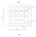
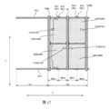
本開示のいくつかの実施例は、表示パネル、特に、透明表示パネルを提供する。図1は、本開示のいくつかの実施例による透明表示パネルの平面概略図であり、図1に示すように、透明表示パネル100は、ベース基板10と、ベース基板10に設けられ陳列して配列された複数の画素Pを含む。画素アレイの行方向は例えば第1の方向Xであり、列方向は例えば第2の方向Yであり、第1の方向Xと第2の方向Yとは互いに交差し、例えば直交する。Some embodiments of the present disclosure provide a display panel, in particular a transparent display panel. FIG. 1 is a schematic plan view of a transparent display panel according to some embodiments of the present disclosure. As shown in FIG. 1, the
図2は、図1の領域Aの拡大概略図であり、図2には、4つの画素Pのみが示されている。図2に示すように、各画素Pは、光透過領域TAと表示領域DAとを含む。各画素Pにおいて、光透過領域TAと表示領域DAは第1の方向に並んで配列される。本実施例では、図2に示すように、各画素Pにおいて、光透過領域TAと表示領域DAは、左右に配置されており、光透過領域TAは、表示領域DAの左側に位置している。当業者にとって理解されるように、他の実施例では、光透過領域TAは表示領域DAの右側に位置してもよく、いくつかの実施例では、一部の画素において光透過領域TAは表示領域DAの左側に位置し、他の画素において光透過領域TAは表示領域DAの右側に位置してもよい。2 is an enlarged schematic diagram of the region A in FIG. 1, and only four pixels P are shown in FIG. 2. As shown in FIG. 2, each pixel P includes a light-transmitting region TA and a display region DA. In each pixel P, the light-transmitting region TA and the display region DA are arranged side by side in a first direction. In this embodiment, as shown in FIG. 2, in each pixel P, the light-transmitting region TA and the display region DA are arranged side by side, and the light-transmitting region TA is located on the left side of the display region DA. As will be understood by those skilled in the art, in other embodiments, the light-transmitting region TA may be located on the right side of the display region DA, and in some embodiments, the light-transmitting region TA may be located on the left side of the display region DA in some pixels, and the light-transmitting region TA may be located on the right side of the display region DA in other pixels.
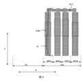
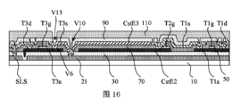
図3は、本開示のいくつかの実施例による画素の表示領域の断面構造概略図を示しており、図3に示すように、画素Pの表示領域DAにおいて、図3に示すように、ベース基板10に第1の金属層20、第1の絶縁層30、アクティブ材料層40、第2の絶縁層50、第2の金属層60、第3の絶縁層70、第3の金属層80、第4の絶縁層90、第5の絶縁層110、第1の電極層120、画素定義層130、発光材料層140、第2の電極層150、封止層160、カラーフィルム層CF、ブラックマトリックス層BM、及び封止カバー170がこの順に配置される。いくつかの実施例において、第4の絶縁層90は、省略される。Figure 3 shows a schematic cross-sectional structure of a display area of a pixel according to some embodiments of the present disclosure. As shown in Figure 3, in the display area DA of a pixel P, a
ベース基板10及び封止カバー170は、例えば、光透過特性が良好なガラス材料で作製され、第1の絶縁層30は、例えば、バッファ層であり、本明細書においてバッファ層30と称してもよく、第2の絶縁層50は、例えば、ゲート絶縁層であり、本明細書においてゲート絶縁層50と称してもよく、第3の絶縁層70は、例えば、層間誘電体層であり、本明細書において層間誘電体層70と称してもよく、第4の絶縁層90は、例えば、パッシベーション層であり、本明細書においてパッシベーション層90と称してもよい。第5の絶縁層110は、例えば平坦化層であり、本明細書において平坦化層110と称してもよい。平坦化層110は、例えば樹脂などの有機材料によって形成され、画素定義層130も有機材料によって形成される。いくつかの実施例において、平坦化層110自体が絶縁の役割を有するため、パッシベーション層90を設置しなくてもよい。The
図3は、画素表示領域の単一のサブ画素の断面層構造を模式的に示したものであり、表示領域が有する層を示すためのものであり、平面図における各層の具体的な位置を示すものではないことが理解される。It will be understood that Figure 3 is a schematic diagram showing the cross-sectional layer structure of a single subpixel in the pixel display region, and is intended to show the layers that the display region has, and does not show the specific positions of each layer in a plan view.
図3に示すように、単一のサブ画素は駆動トランジスタDTを含み、第1の金属層20はシールド層21を含み、前記アクティブ材料層40は駆動トランジスタDTのアクティブ層41を含み、前記シールド層は駆動トランジスタDTのアクティブ層41をシールドし、外光が駆動トランジスタDTのアクティブ層41に入射してサブ画素の表示に悪影響を及ぼすことを防止することができる。第2の金属層60は、駆動トランジスタDTのゲート61を含み、第3の金属層80は、駆動トランジスタDTの例えばドレイン等の第1の電極81と、ソース等の第2の電極82とを含む。第1の電極層120は、例えばアノード層であり、ここではアノード層120とも呼ばれ、サブ画素内の発光素子Dのアノードを含む。第2の電極層150は、例えばカソード層であり、本明細書ではカソード層150とも称され、サブ画素における発光素子Dのカソードを含む。例示として、封止層160は、ベース基板10と垂直な方向に順次に積層された第1の無機層161、有機層162、及び第2の無機層163を含むことができる。As shown in FIG. 3, a single subpixel includes a drive transistor DT, a
いくつかの実施例において、カラーフィルム層CF及びブラックマトリックスBMは、カバー170に予め形成され、カラーフィルム層CF及びブラックマトリックスBMが形成されたカバー170と、ベース基盤10に封止層160が形成された表示基板とを、位置合わせて貼り合わせ、透明表示パネル100を形成することができる。代替的な実施例において、カラーフィルム層CFは、ベース基板10を含む表示基板に設置され、例えば、封止層160に直接に設置され、または平坦化層110と第3の金属層80との間に位置してもよく、そして、カバー170と表示基板とを位置合わせて貼り合わせ、透明表示パネル100を形成することができる。いくつかの実施例において、ブラックマトリックスBMは、さらに互いに異なる色の積層されたカラーフィルタ層CFで代替しでもよい。In some embodiments, the color film layer CF and the black matrix BM can be pre-formed on the
いくつかの実施例において、発光材料層140は蒸着により全面的に形成され、図3に示すように、例えば、発光素子Dはいずれも白色光を発光し、カラーフィルム層CFは、異なるサブ画素に対応する領域において異なる色を透過することにより、カラー表示を実現する。In some embodiments, the light-emitting
いくつかの実施例において、発光材料層140は、印刷で画素定義層130の開口領域に形成され、異なる色のサブ画素は、異なる色の光を発光する発光材料層140を印刷することができ、この場合、カラーフィルム層CFは省略され、さらに、カバー170及びブラックマトリックスも省略され得る。In some embodiments, the light-emitting
いくつかの実施例において、光を透過しないか又は光透過効果がよくない第1の金属層20、第2の金属層60、第3の金属層80、アノード層120、平坦化層110、画素定義層130、ブラックマトリクスBM、及びカラーフィルム層CFのうちの少なくとも1つの層は、光透過領域TAに設けられず、例えば、上記の各層はいずれも光透過領域TAに設けられず、光透過領域TAの透明効果を保障する。In some embodiments, at least one of the
以下の実施例では、透明表示パネルにおける単一画素構成と、単一画素の画素駆動回路について詳細に説明する。The following example provides a detailed description of a single pixel configuration in a transparent display panel and a pixel drive circuit for a single pixel.
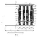
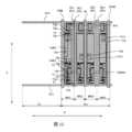
図4は、図2の領域Bの拡大概略図であり、本開示のいくつかの実施例による単一画素の表示領域の平面構造概略図を示し、図4に示すように、画素Pの表示領域DAは、第1のサブ画素、第2のサブ画素、第3のサブ画素および第4のサブ画素という4つのサブ画素を含み、例えば、4つのサブ画素はそれぞれ赤色サブ画素、緑色サブ画素、青色サブ画素及び白色サブ画素であることができる。当業者が理解されるように、各サブ画素がサブ画素駆動回路と、サブ画素駆動回路に位置する発光素子Dとを備え、そして、各サブ画素のサブ画素駆動回路がその対応的な発光素子Dを駆動できるように確保されていれば、4つのサブ画素の発光素子は、実際の必要に応じてその形状及び配置を調整することができる。本技術分野において、画素定義層は、発光素子の発光領域の位置および形状を制限し、前記発光素子の発光材料層は画素定義層の開口に配置され、実際の必要に応じて画素定義層の開口位置および形状を調整して、有機発光素子の発光材料層の位置および形状を調整することができる。Figure 4 is an enlarged schematic diagram of region B in Figure 2, showing a schematic planar structure of the display area of a single pixel according to some embodiments of the present disclosure. As shown in Figure 4, the display area DA of the pixel P includes four subpixels, namely a first subpixel, a second subpixel, a third subpixel and a fourth subpixel. For example, the four subpixels can be red subpixels, green subpixels, blue subpixels and white subpixels, respectively. As will be understood by those skilled in the art, as long as each subpixel has a subpixel driving circuit and a light-emitting element D located in the subpixel driving circuit, and the subpixel driving circuit of each subpixel is ensured to drive its corresponding light-emitting element D, the light-emitting elements of the four subpixels can adjust their shapes and arrangements according to actual needs. In the present technical field, the pixel definition layer limits the position and shape of the light-emitting area of the light-emitting element, and the light-emitting material layer of the light-emitting element is disposed in the opening of the pixel definition layer, and the position and shape of the opening of the pixel definition layer can be adjusted according to actual needs to adjust the position and shape of the light-emitting material layer of the organic light-emitting element.
各サブ画素の構造及び位置関係を明確に表現するために、図4では、各サブ画素の発光素子及び各発光素子を取り囲む画素定義層を図示していない。主に第1のサブ画素、第2のサブ画素、第3のサブ画素及び第4のサブ画素のサブ画素駆動回路、すなわち第1のサブ画素駆動回路SPC1、第2のサブ画素駆動回路SPC2、第3のサブ画素駆動回路SPC3及び第4のサブ画素駆動回路SPC4を示したが、図4に示すように、第1のサブ画素駆動回路SPC1、第2のサブ画素駆動回路SPC2、第3のサブ画素駆動回路SPC3及び第4のサブ画素駆動回路SPC4はいずれも第2の方向Yに延在し、画素Pにおいて第1の方向Xに順次並んで配列されており、第1のサブ画素駆動回路SPC1、第2のサブ画素駆動回路SPC2、第3のサブ画素駆動回路SPC3及び第4のサブ画素駆動回路SPC4が画素Pの画素駆動回路を構成している。したがって、図4を、本開示のいくつかの実施例による単一画素に対する画素駆動回路の構成概略図としてもよい。本実施例では、第1のサブ画素駆動回路SPC1、第2のサブ画素駆動回路SPC2、第3のサブ画素駆動回路SPC3、及び第4のサブ画素駆動回路SPC4が、前記画素Pの光透過領域TAから順に離れて並んでいる。In order to clearly show the structure and positional relationship of each subpixel, FIG. 4 does not show the light-emitting element of each subpixel and the pixel definition layer surrounding each light-emitting element. Although the subpixel driving circuits of the first subpixel, the second subpixel, the third subpixel, and the fourth subpixel, that is, the first subpixel driving circuit SPC1, the second subpixel driving circuit SPC2, the third subpixel driving circuit SPC3, and the fourth subpixel driving circuit SPC4, are mainly shown, as shown in FIG. 4, the first subpixel driving circuit SPC1, the second subpixel driving circuit SPC2, the third subpixel driving circuit SPC3, and the fourth subpixel driving circuit SPC4 all extend in the second direction Y and are arranged in sequence in the first direction X in the pixel P, and the first subpixel driving circuit SPC1, the second subpixel driving circuit SPC2, the third subpixel driving circuit SPC3, and the fourth subpixel driving circuit SPC4 constitute the pixel driving circuit of the pixel P. 4 may be a schematic diagram of a pixel driving circuit for a single pixel according to some embodiments of the present disclosure. In this embodiment, a first subpixel driving circuit SPC1, a second subpixel driving circuit SPC2, a third subpixel driving circuit SPC3, and a fourth subpixel driving circuit SPC4 are arranged in order away from the light transmission area TA of the pixel P.
本実施例では4つのサブ画素を有する画素構造を例に挙げて説明したが、当業者にとって理解されるように、他の実施例では、単一画素は他の数のサブ画素、例えば赤色サブ画素、緑色サブ画素及び青色サブ画素という3つのサブ画素を有してもよい。Although the present embodiment is described with reference to a pixel structure having four subpixels, those skilled in the art will appreciate that in other embodiments, a single pixel may have other numbers of subpixels, for example, three subpixels: a red subpixel, a green subpixel, and a blue subpixel.
図5は、本開示の実施例による単一サブ画素の回路図であり、以下、図4及び図5に関連して、本開示の実施例による単一画素Pについて解釈して説明する。Figure 5 is a circuit diagram of a single subpixel according to an embodiment of the present disclosure, and below, a single pixel P according to an embodiment of the present disclosure will be explained in relation to Figures 4 and 5.
図4に示すように、各画素Pは、1本の第1のゲート線GL1、1本の第2のゲート線GL2、1本の第1の電源線VDDL、1本の第2の電源線VSSL、1本の検出線SL、及び、4本のデータラインDLに対応している。図5に示すように、第1のサブ画素駆動回路SPC1、第2のサブ画素駆動回路SPC2、第3のサブ画素駆動回路SPC3、及び第4のサブ画素駆動回路SPC4のそれぞれは、第1のトランジスタT1(スイッチングトランジスタT1ともいう)、第2のトランジスタT2(駆動トランジスタT2ともいう)、及び第3のトランジスタT3(検出トランジスタT3ともいう)、及び蓄積容量Cstを備えている。第1のゲート線GL1は各サブ画素駆動回路に第1の制御信号G1を提供し、第2のゲート線GL2は各サブ画素に第2の制御信号G2を提供し、第1のデータラインDL1、第2のデータラインDL2、第3のデータラインDL3及び第4のデータラインDL4はそれぞれ第1のサブ画素駆動回路SPC1、第2のサブ画素駆動回路SPC2、第3のサブ画素駆動回路SPC3及び第4のサブ画素駆動回路SPC4にデータ信号Dataを提供し、第1の電源線VDDLは各サブ画素駆動回路に一定の第1の電圧信号、例えばVDD電圧信号を提供し、第2の電源線VSSLは各サブ画素駆動回路に一定の第2の電圧信号、例えばVSS電圧信号を提供する。検出線SLは、各画素駆動回路にリセット信号を提供するとともに、例えば第2のトランジスタT2の閾値電圧の各サブ画素駆動回路の電気的な特性をサンプリング検出することにより、外部補償を行い、良好な表示効果を取得する。As shown in Fig. 4, each pixel P corresponds to one first gate line GL1, one second gate line GL2, one first power supply line VDDL, one second power supply line VSSL, one detection line SL, and four data lines DL. As shown in Fig. 5, each of the first subpixel driving circuit SPC1, the second subpixel driving circuit SPC2, the third subpixel driving circuit SPC3, and the fourth subpixel driving circuit SPC4 includes a first transistor T1 (also called a switching transistor T1), a second transistor T2 (also called a driving transistor T2), a third transistor T3 (also called a detection transistor T3), and a storage capacitance Cst. The first gate line GL1 provides a first control signal G1 to each subpixel driving circuit, the second gate line GL2 provides a second control signal G2 to each subpixel, the first data line DL1, the second data line DL2, the third data line DL3 and the fourth data line DL4 respectively provide a data signal Data to the first subpixel driving circuit SPC1, the second subpixel driving circuit SPC2, the third subpixel driving circuit SPC3 and the fourth subpixel driving circuit SPC4, the first power supply line VDDL provides a constant first voltage signal, for example a VDD voltage signal, and the second power supply line VSSL provides a constant second voltage signal, for example a VSS voltage signal, to each subpixel driving circuit. The detection line SL provides a reset signal to each pixel driving circuit, and performs external compensation by sampling and detecting the electrical characteristics of each subpixel driving circuit, for example the threshold voltage of the second transistor T2, to obtain a good display effect.
具体的には、各サブ画素駆動回路は、スイッチングトランジスタT1、駆動トランジスタT2、検出トランジスタT3、および蓄積容量Cstを有する。駆動トランジスタT2は、図3の駆動トランジスタDTであり、スイッチングトランジスタT1のゲートは、第1のゲート線GL1によって提供される第1の制御信号G1を受信し、スイッチングトランジスタT1の第1の電極は、例えばドレインであり、データラインDLによって提供されるデータ信号Dataを受信し、スイッチングトランジスタT1の第2の電極は、例えばソースであり、蓄積容量Cstの第2の容量電極CstE2および駆動トランジスタT2のゲートに電気的に接続され、これらの三者は、第1のノードGで電気的に接続され、スイッチングトランジスタT1は、第1の制御信号G1に応答して駆動トランジスタT2のゲートおよび蓄積容量Cstにこのデータ信号Dataを書き込むように配置される。Specifically, each subpixel driving circuit has a switching transistor T1, a driving transistor T2, a detection transistor T3, and a storage capacitance Cst. The driving transistor T2 is the driving transistor DT in FIG. 3, the gate of the switching transistor T1 receives a first control signal G1 provided by a first gate line GL1, the first electrode of the switching transistor T1 is, for example, a drain and receives a data signal Data provided by a data line DL, the second electrode of the switching transistor T1 is, for example, a source and is electrically connected to the second capacitance electrode CstE2 of the storage capacitance Cst and the gate of the driving transistor T2, these three are electrically connected at a first node G, and the switching transistor T1 is arranged to write this data signal Data to the gate of the driving transistor T2 and the storage capacitance Cst in response to the first control signal G1.
駆動トランジスタT2の第1の電極は、例えば、ドレインであり、第1の電源接続線VDDLSによって第1の電源線VDDLに電気的に接続され、第1の電源線VDDLから提供される第1の電圧信号、例えば、VDD電圧信号を受信し、駆動トランジスタT2の第2の電極は、例えば、ソースであり、蓄積容量Cstの第2の容量電極CstE2に電気的に接続され、発光素子Dのアノードに電気的に接続されるように配置され、駆動トランジスタT2は、駆動トランジスタT2のゲートの電圧の制御によって発光素子Dを駆動するための電流を制御するように配置される。The first electrode of the driving transistor T2 is, for example, a drain, electrically connected to the first power supply line VDDL by the first power supply connection line VDDLS, and receives a first voltage signal, for example, a VDD voltage signal, provided from the first power supply line VDDL; the second electrode of the driving transistor T2 is, for example, a source, electrically connected to the second capacitance electrode CstE2 of the storage capacitance Cst, and arranged to be electrically connected to the anode of the light-emitting element D; and the driving transistor T2 is arranged to control the current for driving the light-emitting element D by controlling the voltage of the gate of the driving transistor T2.
検出トランジスタT3のゲートは、第2のゲート線GL2から提供される第2の制御信号G2を受信し、検出トランジスタT3の第1の電極は、例えばソースであり、駆動トランジスタT2の第2の電極及び蓄積容量Cstの第1の容量電極CstE1に電気的に接続され、三者は、第2のノードSで電気的に接続され、検出トランジスタT3の第2の電極は、例えばドレインであり、検出接続線SLSによって検出線SLに電気的に接続され、検出線SLからリセット信号を取得し、検出線SLにサンプリング検出信号SENを提供し、検出トランジスタT3は、第2の制御信号G2に応答して前記サブ画素駆動回路の電気的特性を検出して外部補償を実現するように配置され、当該電気的な特性は、例えば、スイッチングトランジスタT1の閾値電圧、及び/又は、キャリア遷移率、あるいは発光素子の閾値電圧、駆動電流などを含む。The gate of the detection transistor T3 receives a second control signal G2 provided from the second gate line GL2, and the first electrode of the detection transistor T3 is, for example, a source, and is electrically connected to the second electrode of the driving transistor T2 and the first capacitance electrode CstE1 of the storage capacitance Cst, the three being electrically connected at a second node S, and the second electrode of the detection transistor T3 is, for example, a drain, and is electrically connected to the detection line SL by the detection connection line SLS, and obtains a reset signal from the detection line SL and provides a sampling detection signal SEN to the detection line SL, and the detection transistor T3 is arranged to detect the electrical characteristics of the subpixel driving circuit in response to the second control signal G2 to realize external compensation, and the electrical characteristics include, for example, the threshold voltage and/or the carrier transition rate of the switching transistor T1, or the threshold voltage and driving current of the light-emitting element.
発光素子Dのアノードは、駆動トランジスタT2の第2の電極、例えばソースに電気的に接続され、発光素子Dのカソードは、第2の電源線VSSLに電気的に接続され、例えばスルーホールによって電気的に接続されてVSS電圧信号が入力される。発光素子Dは、これに流れる電流に基づいて発光を実現し、発光強度は発光素子Dに流れる電流の強度によって定まる。The anode of the light-emitting element D is electrically connected to the second electrode, for example the source, of the driving transistor T2, and the cathode of the light-emitting element D is electrically connected to the second power line VSSL, for example electrically connected by a through-hole to input a VSS voltage signal. The light-emitting element D emits light based on the current flowing therethrough, and the light emission intensity is determined by the intensity of the current flowing through the light-emitting element D.
いくつかの実施例では、蓄積容量Cstは、第1の容量電極CstE1に電気的に接続された第3の容量電極CstE3を備える。第1の容量電極CstE1、第2の容量電極CstE2及び第3の容量電極CstE2は、ベース基板10に順に積層されている。第1の容量電極CstE1と第2の容量電極CstE2は、互いに重なる領域を有し、第1の容量電極CstE1と第2の容量電極CstE2は、第1の容量を構成する。第3の容量電極CstE3と第2の容量電極CstE2は、互いに重なる領域を有し、第3の容量電極CstE3と第2の容量電極CstE2は、第2の容量を構成し、蓄積容量Cstは第1の容量及び第2の容量の並列接続と見ることができ、これによって、蓄積容量Cstの容量値が増加する。In some embodiments, the storage capacitance Cst includes a third capacitance electrode CstE3 electrically connected to the first capacitance electrode CstE1. The first capacitance electrode CstE1, the second capacitance electrode CstE2, and the third capacitance electrode CstE2 are stacked in order on the
本開示の実施例で用いられるトランジスタは、薄膜トランジスタ又は電界効果トランジスタ又は他の特性が同じスイッチング素子であってもよく、本開示の実施例では、薄膜トランジスタを例に説明する。ここで用いられるトランジスタのソース、ドレインは、構造的に対称であることができ、そのソース、ドレインは構造的に区別がなくてもよい。本開示の実施例において、トランジスタのゲート以外の2つの電極を区別するために、その一方の電極が第1の電極であり、他方の電極が第2の電極であることが直接的に説明される。また、トランジスタの特性に応じて、トランジスタをN型トランジスタおよびP型トランジスタに分けることができる。トランジスタがP型トランジスタである場合、ターンオン電圧はローレベル電圧(例えば、0V、-5V、-10V、またはその他の適切な電圧)であり、ターンオフ電圧はハイレベル電圧(例えば、5V、10V、またはその他の適切な電圧)であり、トランジスタがN型トランジスタである場合、ターンオン電圧は、ハイレベル電圧(例えば、5V、10V、又は他の適切な電圧)であり、ターンオフ電圧は、ローレベル電圧(例えば、0V、-5V、-10V、又は他の適切な電圧)である。なお、本明細書における説明では、トランジスタがN型トランジスタである例を用いて説明するが、本開示を限定するものではない。The transistors used in the embodiments of the present disclosure may be thin film transistors or field effect transistors or other switching elements with the same characteristics, and in the embodiments of the present disclosure, thin film transistors are used as an example. The source and drain of the transistor used here may be structurally symmetrical, and the source and drain may not be structurally distinct. In the embodiments of the present disclosure, in order to distinguish between two electrodes other than the gate of the transistor, it is directly explained that one electrode is a first electrode and the other electrode is a second electrode. In addition, according to the characteristics of the transistor, the transistors can be divided into N-type transistors and P-type transistors. If the transistor is a P-type transistor, the turn-on voltage is a low level voltage (e.g., 0V, -5V, -10V, or other suitable voltage), and the turn-off voltage is a high level voltage (e.g., 5V, 10V, or other suitable voltage), and if the transistor is an N-type transistor, the turn-on voltage is a high level voltage (e.g., 5V, 10V, or other suitable voltage), and the turn-off voltage is a low level voltage (e.g., 0V, -5V, -10V, or other suitable voltage). In the explanations in this specification, we use examples in which the transistors are N-type transistors, but this is not intended to limit the scope of the present disclosure.
図4に示すように、単一画素Pの対応領域内、すなわち図4に示す範囲内では、第1のゲート線GL1及び第2のゲート線GL2はいずれも第1の方向Xに延び、例えば直線状となり、第1のゲート線GL1及び第2のゲート線GL2はそれぞれ光透過領域TAの両側に設けられ、すなわち光透過領域TAは第1のゲート線GL1と第2のゲート線GL2の間に挟まれる。他の実施例において、第1のゲート線GL1及び第2のゲート線GL2は光透過領域TA内に穿設されてもよい。単一画素Pの対応領域内、すなわち図4に示す範囲内では、第1の電源線VDDL、第2の電源線VSSL、検出線SL及び4本のデータラインDLはいずれも第2の方向Yに延び、例えば直線状となる。具体的には、検出線SLは、第2のサブ画素駆動回路SPC2、第3のサブ画素駆動回路SPC3の間に位置している。第1のデータラインDL1及び第2のデータラインDL2は、第1のサブ画素駆動回路SPC1と第2のサブ画素駆動回路SPC2との間に設けられ、第1のデータラインDL1は第2のデータラインDL2よりも第1のサブ画素駆動回路SPC1に近く、第2のデータラインDL2は第1のデータラインDL1よりも第2のサブ画素駆動回路SPC2に近く、すなわち、第1のデータラインDL1は第1のサブ画素駆動回路SPC1と第2のデータラインDL2との間に位置し、第2のデータラインDL2は第1のデータラインDL1と第2のサブ画素駆動回路SPC2との間に位置する。第3のデータラインDL3及び第4のデータラインDL4は、第3のサブ画素駆動回路SPC3と第4のサブ画素駆動回路SPC4との間に設けられ、第3のデータラインDL3は第4のデータラインDL4よりも第3のサブ画素駆動回路SPC3に近く、第4のデータラインDL4は第3のデータラインDL3よりも第4のサブ画素駆動回路SPC4に近く、すなわち、第3のデータラインDL3は第3のサブ画素駆動回路SPC3と第4のデータラインDL4との間に位置し、第4のデータラインDL4は第3のデータラインDL3と第4のサブ画素駆動回路SPC4との間に位置する。第2の電源線VSSLは、第1のサブ画素駆動回路SPC1の第1のデータラインDL1から遠い側、すなわち光透過領域TAと第1のサブ画素駆動回路SPC1との間に位置し、第1の電源線VDDLは、第4のサブ画素駆動回路SPC4の第4のデータラインDL4から遠い側に位置する。本実施例では、第1のサブ画素駆動回路SPC1の構成と第4のサブ画素駆動回路SPC4の構成とが検出線SLに対して鏡面対称であり、第2のサブ画素駆動回路SPC2の構成と第3のサブ画素駆動回路SPC3の構成とが検出線SLに対して鏡面対称である。As shown in FIG. 4, within the corresponding region of the single pixel P, i.e., within the range shown in FIG. 4, the first gate line GL1 and the second gate line GL2 all extend in the first direction X, for example, linearly, and the first gate line GL1 and the second gate line GL2 are provided on both sides of the light-transmitting region TA, i.e., the light-transmitting region TA is sandwiched between the first gate line GL1 and the second gate line GL2. In other embodiments, the first gate line GL1 and the second gate line GL2 may be drilled in the light-transmitting region TA. Within the corresponding region of the single pixel P, i.e., within the range shown in FIG. 4, the first power line VDDL, the second power line VSSL, the detection line SL, and the four data lines DL all extend in the second direction Y, for example, linearly. Specifically, the detection line SL is located between the second subpixel driving circuit SPC2 and the third subpixel driving circuit SPC3. The first data line DL1 and the second data line DL2 are arranged between the first subpixel driving circuit SPC1 and the second subpixel driving circuit SPC2, and the first data line DL1 is closer to the first subpixel driving circuit SPC1 than the second data line DL2, and the second data line DL2 is closer to the second subpixel driving circuit SPC2 than the first data line DL1. That is, the first data line DL1 is located between the first subpixel driving circuit SPC1 and the second data line DL2, and the second data line DL2 is located between the first data line DL1 and the second subpixel driving circuit SPC2. The third data line DL3 and the fourth data line DL4 are provided between the third subpixel driving circuit SPC3 and the fourth subpixel driving circuit SPC4, the third data line DL3 is closer to the third subpixel driving circuit SPC3 than the fourth data line DL4, and the fourth data line DL4 is closer to the fourth subpixel driving circuit SPC4 than the third data line DL3, i.e., the third data line DL3 is located between the third subpixel driving circuit SPC3 and the fourth data line DL4, and the fourth data line DL4 is located between the third data line DL3 and the fourth subpixel driving circuit SPC4. The second power supply line VSSL is located on the side of the first subpixel driving circuit SPC1 far from the first data line DL1, i.e., between the light transmitting area TA and the first subpixel driving circuit SPC1, and the first power supply line VDDL is located on the side of the fourth subpixel driving circuit SPC4 far from the fourth data line DL4. In this embodiment, the configuration of the first subpixel driving circuit SPC1 and the configuration of the fourth subpixel driving circuit SPC4 are mirror symmetrical with respect to the detection line SL, and the configuration of the second subpixel driving circuit SPC2 and the configuration of the third subpixel driving circuit SPC3 are mirror symmetrical with respect to the detection line SL.
図4、図6~図14は、本開示の実施例の表示パネルの製造過程の概略図であり、透明表示パネルの1つの画素Pの構造を示し、本実施例において、透明表示パネルがトップエミッション型OLED表示パネルである場合を例に挙げて説明する。単一画素Pは、表示領域DA及び光透過領域TAを含み、表示領域DAには、光透過領域TAから順次遠くに配列された第1のサブ画素駆動回路SPC1、第2のサブ画素駆動回路SPC2、第3のサブ画素駆動回路SPC3及び第4のサブ画素駆動回路SPC4が設けられ、各々のサブ画素の画素駆動回路は、第1のトランジスタT1、第2のトランジスタT2、第3のトランジスタT3及び蓄積容量Cstを含む。Figures 4, 6 to 14 are schematic diagrams of the manufacturing process of a display panel according to an embodiment of the present disclosure, showing the structure of one pixel P of a transparent display panel. In this embodiment, the transparent display panel is described as a top-emission OLED display panel. The single pixel P includes a display area DA and a light-transmitting area TA. The display area DA includes a first subpixel driving circuit SPC1, a second subpixel driving circuit SPC2, a third subpixel driving circuit SPC3, and a fourth subpixel driving circuit SPC4 arranged in order from the light-transmitting area TA. Each pixel driving circuit of the subpixel includes a first transistor T1, a second transistor T2, a third transistor T3, and a storage capacitance Cst.
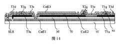
図6は、本開示のいくつかの実施例に係る透明表示パネルの製造工程において、第1の金属層のパターンを形成した後の単一画素の平面構造概略図であり、図7は、図6の線A-Aに沿った断面構造概略図である(なお、図6の線A-Aによる切断位置は、以下の他の図の線A-Aによる切断位置と一致する)。図6および図7に示すように、まず、ベース基板に第1の金属層20のパターンを形成する。具体的に、ベース基板10に第1の金属フィルムを蒸着し、パターニング工程を通じて第1の金属フィルムをパターニングし、ベース基板10にシールド層21及び検出接続線SLSを含む第1の金属層20のパターンを形成する。各サブ画素駆動回路は、1つのシールド層21を含んでおり、検出接続線SLSは、4つのサブ画素駆動回路に跨って第1の方向Xに延在する帯状構造となっている。検出接続線SLSは、後に形成される検出線SLに接続されるように配置され、これにより、検出線SLが各サブ画素駆動回路にリセット信号を提供し、各サブ画素駆動回路の電気的な特性、例えば第2のトランジスタT2の閾値電圧をサンプリング検出し、外部補償を実現する。いくつかの実施例では、シールド層21は、細長い矩形であり、第2の方向Yに延在する。シールド層21は、後に形成される各トランジスタのチャネルに対して遮光処理を行うように配置され、これにより、トランジスタに照射される光強度を低減し、リーク電流を低減して、トランジスタ特性への光照射の影響を低減する。シールド層21の中央部(点線枠で囲んだ部分)は、第1の容量の一方の容量電極、すなわち第1の容量電極CstE1とし、後に形成される第2の容量電極CstE2とで第1の容量を形成するように配置されている。第2の方向Yにおいて、シールド層21の長さは、後に形成されるスイッチングトランジスタT1のゲートと検出トランジスタT3のゲートとの間の距離よりも長い。いくつかの実施例において、シールド層21の長さは、後に形成されるスイッチングトランジスタT1のドレインと第3のトランジスタT3のドレインとの間の距離よりも長い。図4及び図6を参照すると、第1のサブ画素駆動回路SPC1における第1の金属層20のパターンと第4のサブ画素駆動回路SPC4における第1の金属層20のパターンとは、後に形成される検出線SLに対して鏡面対称である。第2のサブ画素駆動回路SPC2における第1の金属層20のパターンと、第3のサブ画素駆動回路SPC3における第1の金属層20のパターンとは、後に形成される検出線SLに対して鏡像対称である。このパターニング工程の後、表示領域DAにはシールド層21及び検出接続線SLSが形成され、光透過領域TAには第1の金属層が配置されない。6 is a schematic diagram of a planar structure of a single pixel after forming a pattern of a first metal layer in a manufacturing process of a transparent display panel according to some embodiments of the present disclosure, and FIG. 7 is a schematic diagram of a cross-sectional structure along line A-A in FIG. 6 (note that the cutting position along line A-A in FIG. 6 coincides with the cutting position along line A-A in the other figures below). As shown in FIG. 6 and FIG. 7, first, a pattern of a
図8は、本開示のいくつかの実施例に係る透明表示パネルの製造工程において、アクティブ材料層のパターンを形成した後の単一画素の平面構造概略図であり、図9は、図8のA-Aに沿った断面構造概略図である。次に、図8及び図9に示すように、アクティブ材料層40のパターンを形成し、具体的には、前記パターンが形成されたベース基板10に、第1の絶縁フィルム及び例えば金属酸化物フィルムというアクティブ材料フィルムを順次蒸着し、パターニング工程によりアクティブ材料フィルムをパターニングして、第1の金属層20のパターンを覆う第1の絶縁層30および第1の絶縁層30に形成されたアクティブ材料層40のパターンを形成する。アクティブ材料層40は、各サブ画素駆動回路に設けられたスイッチングトランジスタT1のアクティブ層(第1のアクティブ層T1aともいう)、駆動トランジスタT2のアクティブ層(第2のアクティブ層T2aともいう)、検出トランジスタT3のアクティブ層(第3のアクティブ層T3aともいう)、及び第2の容量電極CstE2を含む。第2の容量電極CstE2のベース基板10での正投影と第1の容量電極CstE1のベース基板10での正投影とは、重なる領域があり、第1の容量電極CstE1と第2の容量電極CstE2とが第1の容量を形成する。8 is a schematic planar structure diagram of a single pixel after forming a pattern of an active material layer in a manufacturing process of a transparent display panel according to some embodiments of the present disclosure, and FIG. 9 is a schematic cross-sectional structure diagram along A-A in FIG. 8. Next, as shown in FIG. 8 and FIG. 9, a pattern of an
いくつかの実施例によって、第1のアクティブ層T1a、第2のアクティブ層T2a、及び第3のアクティブ層T3aのベース基板10での正投影と、シールド層21のベース基板10での正投影とが重なる領域があるので、シールド層21は、スイッチングトランジスタT1、駆動トランジスタT2、及び検出トランジスタT3のチャネル領域をシールドし、チャネルへの光の影響を避け、漏れ電流の発生によるチャネルの影響によって表示効果に影響を与えることを防止することができる。第1のアクティブ層T1a、第2のアクティブ層T2a、第3のアクティブ層T3a及び第2の容量電極CstE2のいずれか二方は、間隔を置いて設置され、すなわち、第1のアクティブ層T1aのベース基板10での正投影、第2のアクティブ層T2aのベース基板10での正投影、第3のアクティブ層T3aのベース基板10での正投影、及び第2の容量電極CstE2のベース基板10での正投影の間に、重なる領域がない。これにより、関連要求に応じて、スイッチングトランジスタT1、駆動トランジスタT2及び検出トランジスタT3のチャネルのアスペクト比を設計することができる。いくつかの実施例において、図8及び図9に示すように、第1のサブ画素駆動回路SPC1及び第4のサブ画素駆動回路SPC4における第2の容量電極CstE2と第3のアクティブ層T3aとの間に間隔領域42が設けられ、第2のサブ画素駆動回路SPC2及び第3のサブ画素駆動回路SPC3の第2の容量電極CstE2の途中には、切欠領域43が設けられており、間隔領域42および切欠領域43には、アクティブ材料層40が存在していない。いくつかの実施例において、図4及び図8に示すように、第1のサブ画素駆動回路SPC1のアクティブ材料層40のパターンと第4のサブ画素駆動回路SPC4のアクティブ材料層40のパターンとは、後に形成される検出線SLに対して鏡像対称であり、第2のサブ画素駆動回路SPC2のアクティブ材料層40のパターンと第3のサブ画素駆動回路SPC3のアクティブ材料層40のパターンとは、後に形成される検出線SLに対して鏡像対称である。このパターニング工程の後、アクティブ材料層40のパターンは、表示領域DAに形成され、ベース基板10およびベース基板10に設けられた第1の絶縁層30を含む光透過領域TAに形成されていない。In some embodiments, there is an overlapping area between the orthogonal projection of the first active layer T1a, the second active layer T2a, and the third active layer T3a on the
図10は、本開示のいくつかの実施例に係る透明表示パネルの製造工程において、第2の金属層のパターンを形成した後の単一画素の平面構造概略図であり、図11は、図10の線A-Aに沿った断面構造概略図である。図10および図11に示すように、第2の金属層60のパターンを形成し、以下の工程を含む。前記パターンが形成されたベース基板10に、第2の絶縁フィルムおよび第2の金属フィルムを順次蒸着し、パターニング工程により第2の絶縁フィルムおよび第2の金属フィルムをパターニングし、第2の絶縁層50のパターンおよび第2の絶縁層50に設けられた第2の金属層60のパターンを形成する。いくつかの実施例において、第2の絶縁層50のパターンと、第2の金属層60のパターンとは、同一のマスクを用いて形成され、同一のパターンを具備している。第2の金属層60のパターンは、各画素Pに対応して形成された第1のゲート線GL1、第2のゲート線GL2、第1の電源接続線VDDLS、第1の補助線62、第2の補助線63、並びに、各サブ画素駆動回路に形成されたスイッチングトランジスタT1のゲート(第1のゲートT1gともいう)、駆動トランジスタT2のゲート(第2のゲートT2gともいう)、検出トランジスタT3のゲート(第3のゲートT3gともいう)を含んでいる。第2の金属層60のパターンは、各サブ画素駆動回路に形成された第1のゲート接続線64及び第2のゲート接続線65も含んでいる。図10に示すように、単一画素Pに対応する領域、すなわち図10に示す領域では、第1のゲート線GL1及び第2のゲート線GL2は平行に設けられ、いずれも第1の方向Xに沿って直線的に延在し、第1のゲート線GL1は光透過領域TAの下側に位置し、第2のゲート線GL2は光透過領域TAの上側に位置している。すなわち光透過領域TAは、第1のゲート線GL1と第2のゲート線GL2との間に介在している。各サブ画素駆動回路も、第1のゲート線GL1と第2のゲート線GL2との間に介在している。10 is a schematic planar structure diagram of a single pixel after forming a pattern of the second metal layer in a manufacturing process of a transparent display panel according to some embodiments of the present disclosure, and FIG. 11 is a schematic cross-sectional structure diagram along line A-A in FIG. 10. As shown in FIGS. 10 and 11, a pattern of the
第1のゲートT1gは、第1の方向Xに延在し、第1のアクティブ層T1aにわたって設けられ、第2の方向Yに延在する第1のゲート接続線64によって、第1のゲート線GL1に電気的に接続されている。具体的には、第1のゲートT1gは、接続端部T1g1と自由端部T1g2とを含み、第1のゲート接続線64は、第1の端部641と第2の端部642とを含む。第1のゲート接続線64の第1の端部641は、第1のゲート線GL1に電気的に接続され、第1のゲート接続線64の第2の端部642は、第1のゲートT1gの接続端部T1g1に電気的に接続される。いくつかの実施例において、第1のゲートT1g1、第1のゲート接続線64、及び第1のゲート線GL1は、一体構造である。第2のゲートT2gは、第1の方向Xに延在し、第2のアクティブ層T2aにわたって設けられ、第2の容量電極CstE2と重なる領域を有する。第3のゲートT3gは、第1の方向Xに延在し、第3のアクティブ層T3aにわたって設けられ、第2の方向Yに延在する第2のゲート接続線65によって、第2のゲート線GL2に電気的に接続されている。具体的には、第3のゲートT3gは、接続端部T3g1及び自由端部T3g2を含み、第2のゲート接続線65は、第1の端部651及び第2の端部652を含む。第2のゲート接続線65の第1の端部651は、第2のゲート線GL2に電気的に接続され、第2のゲート接続線65の第2の端部652は、第3のゲートT3gの接続端部T3g1に電気的に接続されている。いくつかの実施例において、第3のゲートT3g、第2のゲート接続線65、及び第2のゲート線GL2は、一体構造である。The first gate T1g extends in the first direction X and is electrically connected to the first gate line GL1 by a first
第1の補助線62は、第2の電源線VSSLが位置する領域に形成され、第2の方向Yに延在し、後に形成される第2の電源線VSSLに電気的に接続されるように配置されている。これにより、後に形成される第2の電源線VSSLがビアホールを介して第1の補助線62と並列に設けられ、第2の電源線VSSLのインピーダンスを効果的に低減する。いくつかの実施例では、第1の補助線62は、第1のゲートT1gと第3のゲートT3gとの間に配置される。当業者にとって理解されるように、第1の補助線62は必須ではなく、いくつかの実施例では省略可能である。The first
第2の補助線63は、第1の電源線VDDLが位置する領域に形成され、第2の方向Yに延在し、後に形成される第1の電源線VDDLに電気的に接続されるように配置されている。これにより、後に形成される第1の電源線VDDLがビアホールを介して第2の補助線63と並列に設けられ、第1の電源線VDDLのインピーダンスを効果的に低減する。いくつかの実施例では、第2の補助線63は、第1のゲートT1gと第3のゲートT3gとの間に配置される。当業者にとって理解されるように、第2の補助線63は必須ではなく、いくつかの実施例では省略可能である。The second
第1の電源接続線VDDLSは、第1の方向Xに延在し、4つのサブ画素駆動回路にわたって設けられており、後に形成される第1の電源線VDDLに電気的に接続されるように配置されている。いくつかの実施例において、第1の電源接続線VDDLSは第2の補助線63に電気的に接続され、両者は例えば一体構造である。The first power supply connection line VDDLS extends in the first direction X, is provided across the four subpixel driving circuits, and is arranged so as to be electrically connected to the first power supply line VDDL to be formed later. In some embodiments, the first power supply connection line VDDLS is electrically connected to the second
図11に示すように、第2の絶縁層50のパターンは、第2の金属層60のパターンと同じであり、すなわち、第2の絶縁層50は、第2の金属層60の下方に位置し、第2の金属層60以外の領域には、第2の絶縁層50が設けられていない。図10に示すように、第1の電源接続線VDDLSに加えて、第1のサブ画素駆動回路SPC1における第2の金属層のパターンと第4のサブ画素駆動回路SPC4における第2の金属層のパターンとは、後に形成される検出線SLに対して鏡面対称であり、第2のサブ画素駆動回路SPC2における第2の金属層のパターンと第3のサブ画素駆動回路SPC3における第2の金属層のパターンとは、後に形成される検出線SLに対して鏡面対称である。As shown in FIG. 11, the pattern of the second insulating
いくつかの実施例において、この工程は、導体化処理をさらに含む。導体化処理は、第2の金属層60のパターンの形成後、第1のゲートT1g、第2のゲートT2g及び第3のゲートT3gを含む第2の金属層60のパターンをシールドとしてプラズマ処理を行い、第1のゲートT1g、第2のゲートT2g及び第3のゲートT3gによってシールドされた領域のアクティブ材料層40(すなわちアクティブ材料層40と第1のゲートT1g、第2のゲートT2g及び第3のゲートT3gとが重なる領域)をそれぞれトランジスタのチャネル領域とする。第2の金属層60でシールドされていない領域のアクティブ材料層40が導体化され、導体化された第2の容量電極CstE2と導体化されたソースドレイン領域が形成される。今回のパターニング工程の後、第2の金属層60のパターンは、表示領域DAに形成され、光透過領域TAには形成されず、光透過領域TAは、ベース基板10及びベース基板10に設けられた第1の絶縁層30を含む。In some embodiments, this step further includes a conductorization process. In the conductorization process, after the pattern of the
図12は、本開示のいくつかの実施例に係る透明表示パネルの製造工程において、第3の絶縁層のパターンを形成した後の単一画素の平面構造概略図であり、図13は、図12の線A-Aに沿った断面構造概略図である。図12および図13に示すように、次に、第3の絶縁層70のパターンを形成する。第3の絶縁層70のパターンを形成することは、以下の工程を含む。すなわち、上記パターンが形成されたベース基板10に第3の絶縁フィルムを蒸着し、パターニング工程により第3の絶縁フィルムをパターニングして上記構造を覆う第3の絶縁層70のパターンを形成し、第3の絶縁層70に複数のビアホールが設けられており、複数のビアホールは、第1のゲートT1gの両側に位置する第1のビアホールV1と第2のビアホールV2、第2のゲートT2gの両側に位置する第3のビアホールV3と第4のビアホールV4、第3のゲートT3gの両側に位置する第5のビアホールV5と第6のビアホールV6、検出接続線SLSと検出線との交差位置に位置する第7のビアホールV7と、検出接続線SLSと検出トランジスタT3のドレインとの交差位置に位置する第8のビアホールV8、第2のゲートT2gと第2の容量電極CstE2の境界に位置する第9のビアホールV9、アクティブ材料層40が覆われていないシールド層21の位置、例えば、間隔領域42または切欠領域43の位置に位置する第10のビアホールV10、第14のビアホールV14、第1の補助線62の位置に位置する複数の第11のビアホールV11と、第2の補助線63の位置に位置する複数の第12のビアホールV12、を含む。Figure 12 is a schematic diagram of the planar structure of a single pixel after forming a pattern of the third insulating layer in a manufacturing process of a transparent display panel according to some embodiments of the present disclosure, and Figure 13 is a schematic diagram of the cross-sectional structure along line A-A in Figure 12. As shown in Figures 12 and 13, next, a pattern of the third insulating
第1のビアホールV1および第2のビアホールV2内の第3の絶縁層70は、エッチングされ、第1のアクティブ層T1aの両端の表面を露出する。第3のビアホールV3は第1の電源接続線VDDLSと第2のアクティブ層T2aとの境界に配置され、第3のビアホールV3内の第3の絶縁層70はエッチングされ、第2のアクティブ層T2aの表面及び第1の電源接続線VDDLSの表面を露出し、第4のビアホールV4内の第3の絶縁層70はエッチングされ、第2のアクティブ層T2aの表面を露出する。第5のビアホールV5および第6のビアホールV6内の第3の絶縁層70はエッチングされ、第3のアクティブ層T3aの両端の表面を露出する。第7のビアホールV7は、検出接続線SLSと後に形成される検出線SLとが重なる位置に配置され、各サブ画素駆動回路内に1つの第8のビアホールV8が形成され、第7のビアホールV7および第8のビアホールV8内の第1の絶縁層30および第3の絶縁層70はエッチングされ、検出接続線SLSの表面を露出する。第9のビアホールV9は、第2のゲートT2gと第2の容量電極CstE2との境界に位置し、第9のビアホールV9内の第3の絶縁層70がエッチングされ、第2のゲートT2gの表面及び第2の容量電極CstE2の表面を露出する。第1のサブ画素駆動回路SPC1及び第4のサブ画素駆動回路SPC4中の第10のビアホールV10のベース基板10での正投影は、第2の容量電極CstE2と第3のアクティブ層T3aとの間の間隔領域42のベース基板10での正投影内に位置し、第2のサブ画素駆動回路SPC2及び第3のサブ画素駆動回路SPC3中の第10のビアホールV10のベース基板での正投影は、第2の容量電極CstE2の中部の切欠領域43のベース基板10での正投影内に位置する。第10のビアホールV10内の第1の絶縁層30および第3の絶縁層70は、エッチングされ、シールド層21の表面を露出する。The third insulating
第14のビアホールV14内の第3の絶縁層70はエッチングされ、第1の絶縁層30を露出する。第14のビアホールV14は、工程の対称性のために設計され、第2のサブ画素駆動回路SPC2及び第3のサブ画素駆動回路SPC3のみに形成されており、それのベース基板10での正投影は、第2の容量電極CstE2の中部の切欠領域43のベース基板10での正投影内に位置し、第1のサブ画素駆動回路SPC1及び第4のサブ画素駆動回路SPC4に存在しない。以降の工程では、各サブ画素駆動回路にはいずれもアノードに接続するための第13のビアホールV13が形成される。第1のサブ画素駆動回路SPC1及び第4のサブ画素駆動回路SPC4において、後に形成される第13のビアホールV13は、第3の絶縁層70のみを貫通する第6のビアホールV6を覆ってブッシュホールを形成し、第2のサブ画素駆動回路SPC2及び第3のサブ画素駆動回路SPC3において、後に形成される第13のビアホールV13は、切欠領域43に位置し、第10のビアホールV10に近く、サブ画素駆動回路の工程対称性のために、第2のサブ画素駆動回路SPC2及び第3のサブ画素駆動回路SPC3での第13のビアホールV13がある位置に、第1のサブ画素駆動回路SPC1及び第4のサブ画素駆動回路SPC4における第6のビアホールV6と類似する第14のビアホールV14が形成され、これにより、後に形成される第13のビアホールV13は、第14のビアホールV14を覆ってブッシュホールを形成する。第14のビアホールV14は必須ではなく、いくつかの実施例では設けられなくてもよい。The third insulating
第11のビアホールV11は第1の補助線62に位置し、すなわち、の複数の第11のビアホールV11のベース基板10での正投影は、第1の補助線62のベース基板10での正投影内に落ち込む。複数の第11のビアホールV11は離間して設けられ、第11のビアホールV11内の第3の絶縁層70がエッチングされ、第1の補助線62の表面を露出する。The eleventh via hole V11 is located on the first
複数の第12のビアホールV12は、第2の補助線63に位置し、複数の第12のビアホールV12のベース基板10での正投影は、第2の補助線63のベース基板10での正投影内に落ち込む。複数の第12のビアホールV12が離間して設けられ、第12のビアホールV12内の第3の絶縁層70がエッチングされ、第2の補助線63の表面を露出する。今回のパターニング工程の後、複数のビアホールパターンが表示領域DAに形成され、光透過領域TAは、ベース基板10上に積層された第1の絶縁層30と第3の絶縁層70とを含む。The plurality of twelfth via holes V12 are located on the second
図4は、本開示のいくつかの実施例に係る透明表示パネルの製造工程において、第3の金属層のパターンを形成した後の単一画素の平面構造概略図であり、図14は、図4の線A-Aに沿った断面構造概略図である。図4および図14に示すように、次に、第3の金属層80のパターンを形成し、具体的には、上記パターンが形成されたベース基板に、第3の金属フィルムを蒸着し、パターニング工程により、第3金属フィルムをパターニングして、第3の絶縁層70に第3の金属層パターンを形成する。第3の金属層80は、各画素Pに対応する第1の電源線VDDL、第2の電源線VSSL、検出線SL及び4本のデータラインDLと、各サブ画素に形成されたスイッチングトランジスタT1のソース及びドレイン(第1のソースT1s及び第1のドレインT1dともいう)、駆動トランジスタT2のソース及びドレイン(第2のソースT2s及び第2のドレインT2dともいう)、検出トランジスタT3のソース及びドレイン(第3のソースT3s及び第3のドレインT3dともいう)、第3の容量電極CstE3とを備え、図14は、図4の線A-Aに沿う断面概略図である。図4及び図14に示すように、第1のドレインT1d及び第1のソースT1sは、それぞれ第1のビアホールV1及び第2のビアホールV2によって、第1のゲートT1gの両側にある第1のアクティブ層T1aの導体化端部に電気的に接続され、スイッチングトランジスタT1を形成する。第2のドレインT2d及び第2のソースT2sは、それぞれ第3のビアホールV3及び第4のビアホールV4によって、第2のゲートT2gの両側にある第2のアクティブ層T2aの導体化端部に電気的に接続され、駆動トランジスタT2を形成し、そして、第2のドレインT2dは、第3のビアホールV3によって、第1の電源接続線VDDLSに電気的に接続される。第3のドレインT3dと第3のソースT3sは、それぞれ第5のビアホールV5と第6のビアホールV6によによって、第3のゲートT3gの両側にある第3のアクティブ層T3aの導体化端部に電気的に接続され、検出トランジスタT3を形成する。また、第3のドレインT3dは、第8のビアホールV8を介して検出接続線SLSに電気的に接続され、検出線SLは、第7のビアホールを介して、検出接続線SLSに電気的に接続され、これにより、検出線は、各サブ画素駆動回路の検出トランジスタT3のドレインT3dに電気的に接続されている。第1のソースT1sは、図5の第1のノードGと理解すべきである第9のビアホールV9によって、第2のゲートT2g及び第2の容量電極CstE2に電気的に接続される。第3の容量電極CstE3は、第10のビアホールV10によって、シールド層21に電気的に接続され、第14のビアホールV14を充填する。第3の容量電極CstE3は、第2のソースT2s及び第3のソースT3sに電気的に接続されており、一体構造であってもよい。第2の電源線VSSLは、複数の第11のビアホールV11を介して、第1の補助線62に電気的に接続されており、第2の電源線VSSLの伝送抵抗を低減する。第1の電源線VDDLは、複数の第12のビアホールV12を介して、第2の補助線63に電気的に接続され、第1の電源線VDDLの伝送抵抗を低減し、第2の補助線63を介して、第1の電源接続線VDDLSを介して駆動トランジスタT2の第2のドレインT2dにVDD電圧信号を伝達する。図4に示すように、第1のサブ画素駆動回路SPC1における第3の金属層80のパターンと、第4のサブ画素駆動回路SPC4における第3の金属層80のパターンとは、後に形成された検出線SLに対して鏡面対称であり、第2のサブ画素駆動回路SPC2における第3の金属層80のパターンと、第3のサブ画素駆動回路SPC3における第3の金属層80のパターンとは、後に形成された検出線SLに対して鏡面対称である。Figure 4 is a schematic diagram of the planar structure of a single pixel after forming a pattern of the third metal layer in the manufacturing process of a transparent display panel according to some embodiments of the present disclosure, and Figure 14 is a schematic diagram of the cross-sectional structure along line A-A in Figure 4. As shown in Figures 4 and 14, next, a pattern of the
今回のパターニング工程の後、第3の金属層80のパターンは、表示領域DAに形成され、光透過領域TAに形成されず、光透過領域TAは、ベース基板10と、ベース基板10に設けられた第1の絶縁層30、第3の絶縁層70と、を含む。After this patterning process, the pattern of the
図15は、本開示のいくつかの実施例による透明表示パネルの製造工程において、第4の絶縁層及び平坦化層のパターンを形成した後の単一画素の平面構造概略図であり、図16は、図15のA-Aに沿った断面構造概略図である。次に、図15及び図16に示すように、第4の絶縁層90及び平坦化層110のパターンを形成し、具体的には、上記パターンが形成されたベース基板10に、先ず、第4の絶縁フィルムを蒸着し、第4の絶縁フィルムに対するパターニング工程、例えば露光、現像、エッチング等により、各サブ画素駆動回路におけるビアホールを有する第4の絶縁層90のパターンを形成する。そして、第4の絶縁層90のパターンが形成されたベース基板10に平坦化膜を塗布し、平坦化膜に対するパターニング工程、例えば露光、現像、エッチングなどによって、平坦化層110のパターンを形成し、平坦化層110のパターンは、画素Pの表示領域DAにのみ設けられ、光透過領域TAには設けられず、平坦化層110のパターンも各サブ画素駆動回路におけるビアホールを有し、各サブ画素駆動回路において、平坦化層110のビアホールと第4の絶縁層90のビアホールとが整合し、両者が平坦化層110と第4の絶縁層90とを貫通する第13のビアホールV13を構成し、第13のビアホールV13のサイズは、他のビアホールよりも著しく大きい。いくつかの実施例において、図15及び図16に示したように、第1のサブ画素駆動回路SPC1及び第4のサブ画素駆動回路SPC4において、第13のビアホールV13は、検出トランジスタT3のソースT3sの位置に位置し、具体的には、第13のビアホールV13は第6のビアホールV6を覆い、すなわち、第6のビアホールV6のベース基板10での正投影は、第13のビアホールV13のベース基板10での正投影以内に落ち込み、これにより、レイアウトスペースを節約し、後に形成される画素定義層の開口領域を最大限に大きくすることができる。第13のビアホールV13内の第4の絶縁層90および平坦化層110は、エッチングされ、検出トランジスタT3のソースT3sの表面を露出する。第2のサブ画素駆動回路SPC2及び第3のサブ画素駆動回路SPC3において、第13のビアホールV13は、第2の容量電極CstE2の開口43の位置に位置し、第10のビアホールV10に隣接し、いくつかの実施例において、第13のビアホールV13は第14のビアホールV14を覆い、すなわち、第14のビアホールV14のベース基板10での正投影は、ベース基板10への第13のビアホールV13の正投影内に落ち込み、これにより、第1のサブ画素駆動回路SPC1及び第4のサブ画素駆動回路SPC4におけるブッシュホールと類似する構成が形成され、工程の均一性が向上する。第13のビアホールV13内の第4の絶縁層90および平坦化層110は、エッチングされ、第3の容量電極CstE3の表面を露出する。各サブ画素駆動回路において、第13のビアホールV13は、第10のビアホールV10に隣接し、両者は第2の方向Yに面一であり、すなわち、第13のビアホールV13の中心と第10のビアホールV10の中心とを結ぶ直線は、第2の方向Yと平行である。第1のサブ画素駆動回路SPC1及び第4のサブ画素駆動回路SPC4において、第13のビアホールV13は、第10のビアホールV10よりも第2のゲート線GL2に近く、第2のサブ画素駆動回路SPC2及び第3のサブ画素駆動回路SPC3において、第13のビアホールV13は第10のビアホールV10よりも第2のゲート線GL2から遠くなる。当業者にとって理解されるように、各サブ画素駆動回路の第10のビアホールV10は、第4の絶縁層90および平坦化層110によってシールドされるべきであるが、第10のビアホールV10と第13のビアホールV13との位置関係を明確に示すために、図15では、各サブ画素駆動回路の第10のビアホールV10を点線で図示した。図15に示すように、第1のサブ画素駆動回路SPC1における第4の絶縁層90及び平坦化層110のパターンと、第4のサブ画素駆動回路SPC4における第4の絶縁層90及び平坦化層110のパターンとは、後に形成された検出線SLに対して鏡像対称であり、第2のサブ画素駆動回路SPC2における第4の絶縁層90及び平坦化層110のパターンと、第3のサブ画素駆動回路SPC3における第4の絶縁層90及び平坦化層110のパターンとは、後に形成された検出線SLに対して鏡像対称である。今回のパターニング工程の後、光透過領域TAは、ベース基板10に積層された第1の絶縁層30、第3の絶縁層70、第4の絶縁層90を含む。15 is a schematic planar structure diagram of a single pixel after forming a pattern of a fourth insulating layer and a planarization layer in a manufacturing process of a transparent display panel according to some embodiments of the present disclosure, and FIG. 16 is a schematic cross-sectional structure diagram along A-A in FIG. 15. Next, as shown in FIG. 15 and FIG. 16, a pattern of a fourth insulating
図17は、本開示の実施例に係る透明表示パネルの製造工程において、アノード層のパターンを形成した後の単一画素の平面構造概略図であり、図18は、図17の線A-Aに沿った断面構造概略図である。次に、図17および図18に示すように、アノード層120のパターンを形成する。具体的には、上記パターンが形成されたベース基板に、透明導電性薄膜、例えばITO、IZOを積層し、パターニング工程により、透明導電性薄膜をパターニングして、平坦化層110にアノード層120のパターンを形成し、アノード層120は、少なくとも各サブ画素の発光素子Dのアノード1200、すなわち、第1のサブ画素の第1の発光素子の第1のアノード1201、第2のサブ画素の第2の発光素子の第2のアノード1202、第3のサブ画素の第3の発光素子の第3のアノード1203、第4のサブ画素の第4の発光素子の第4のアノード1204を含む。各サブ画素駆動回路における駆動トランジスタT2のソースT2s、検出トランジスタT3のソースT3s及び第3の容量電極CstE3は、互いに接続された一体構造であり、各サブ画素において、アノード1200は、対応するサブ画素駆動回路における第13のビアホールV13(ここではアノードビアホールV13とも呼ぶ)によってこの一体構造に電気的に接続され、これにより、各サブ画素のアノード1200とそのサブ画素駆動回路の駆動トランジスタT2のソースT2sとの電気的接続が実現され、図17において、各サブ画素駆動回路の第13のビアホールV13はアノード1200によってシールドされるべきであるが、第13のビアホールV13とアノード1200との位置関係を明確に示すために、図17では、各サブ画素駆動回路の第13のビアホールV13を点線パターンで示している。いくつかの実施例では、4つのアノード1200はいずれも表示領域DA内に位置し、各アノード1200は、例えば矩形状、ひし形、正方形という四角形であってもよい。他の実施例において、各アノード1200は、例えば円形、多角形などのほかの形状であってもよい。4つのアノード1200は表示領域DA内で2×2マトリクス状に配列される。いくつかの実施例において、図17及び図18に示すように、第1のアノード1201は、左上に位置し、第1のサブ画素駆動回路SPC1の第13のビアホールV13を介して第1のサブ画素駆動回路SPC1の検出トランジスタT3のソースT3sに電気的に接続され、第2のアノード1202は、左下に位置し、第2のサブ画素駆動回路SPC2の第13のビアホールV13を介して第2のサブ画素駆動回路SPC2の第3の容量電極CstE3に電気的に接続され、第3のアノード1203は、右下に位置し、第3のサブ画素駆動回路SPC3の第13のビアホールV13を介して第3のサブ画素駆動回路SPC3の第3の容量電極CstE3に電気的に接続され、第4のアノード1204は、右上に位置し、第4のサブ画素駆動回路SPC4の第13のビアホールV13を介して第4のサブ画素駆動回路SPC4の検出トランジスタT3のソースT3sに電気的に接続されている。17 is a schematic planar structure diagram of a single pixel after forming a pattern of the anode layer in a manufacturing process of a transparent display panel according to an embodiment of the present disclosure, and FIG. 18 is a schematic cross-sectional structure diagram along line A-A in FIG. 17. Next, as shown in FIG. 17 and FIG. 18, a pattern of the
いくつかの可能な実施例によって、表示領域DAにおけるアノード1200の配置方式は、実際の要求に応じて調節されてもよく、本開示では具体的に限定しない。光透過領域TAの光透過率を保障するために、アノード層120は、通常、光透過領域TAに設けられず、今回のパターニング工程後、光透過領域TAの膜層構造は変化しない。According to some possible embodiments, the arrangement manner of the
図19は、本開示のいくつかの実施例に係る透明表示パネルの製造過程において、画素定義層、発光材料層、カソード及び封止層のパターンを形成した後の単一画素の平面構造概略図であり、図20は、図19の線A-Aに沿った断面構造概略図であり、明瞭化のために、図19では、画素定義層、発光材料層、カソード及び封止層パターンを省略し、画素定義層の開口のみを示し、画素定義層、発光材料層、カソード及び封止層は、図20に具現されたものである。図19、図20に示すように、画素定義層、発光材料層、カソード、及び封止層のパターンを形成し、具体的には、前記パターンが形成されたベース基板10に画素定義膜層を塗布し、マスク、露光、及び現像工程によって画素定義層130のパターンを形成し、画素定義層130は、各サブ画素のアノード1200に対応する開口1300、すなわち、第1のアノード1201、第2のアノード1202、第3のアノード1203、及び第4のアノード1204にそれぞれ対応する第1の開口1301、第2の開口1302、第3の開口1303、及び第4の開口1304を有する。第1の開口1301、第2の開口1302、第3の開口1303、第4の開口1304は、それぞれ第1の発光素子、第2の発光素子、第3の発光素子および第4の発光素子の発光領域を制限する。各開口1300のベース基板10での正投影は、その対応アノード1200のベース基板10での正投影内に落ち込み、各開口1300は、その対応アノード1200の一部を露出させる。その後、発光材料層140が、前述のように形成された開口1300内に形成され、対応アノード1200に電気的に接続される。次に、カソードフィルムを堆積し、パターニング工程によりカソード層150のパターンを形成し、カソード層150は、少なくもと各サブ画素の発光素子Dのカソードを含み、カソード層150は、発光材料層140及び第2の電源線VSSLにそれぞれ電気的に接続される。いくつかの実施例において、図19および図20に示すように、各サブ画素の発光素子Dのカソードは一体構造であり、いくつかの実施例によっては、複数の画素Pの各サブ画素の発光素子Dのカソードはすべて一体に形成され、一体構造であり、複数の画素Pの光透過領域TAおよび表示領域DAを覆う。続いて、カソード層150上に、例えば、無機材料/有機材料/無機材料の積層構造からなる封止層160を形成する。いくつかの実施例において、カソード層150は、複数の方式、例えばレーザ穿孔によって、第2の電源線VSSLに電気的に接続されてもよい。今回の工程後、いくつかの実施例において、光透過領域TAは、ベース基板10と、ベース基板10に設けられる第1の絶縁層30、第3の絶縁層70、第4の絶縁層90、カソード層150及び封止層160を含むことができる。当業者にとって理解されるように、光透過領域TAにおける第1の絶縁層30、第3の絶縁層70、第4の絶縁層90、カソード層150及び封止層160はいずれも必須ではなく、いくつかの実施例では、上記各層の形成工程おいて、実際の必要に応じて光透過領域TAにおける上記層を除去してもよい。Figure 19 is a schematic diagram of the planar structure of a single pixel after forming patterns of a pixel definition layer, a light-emitting material layer, a cathode and a sealing layer in the manufacturing process of a transparent display panel according to some embodiments of the present disclosure, and Figure 20 is a schematic diagram of the cross-sectional structure along line A-A in Figure 19. For clarity, the pixel definition layer, light-emitting material layer, cathode and sealing layer patterns are omitted in Figure 19, and only the opening of the pixel definition layer is shown, and the pixel definition layer, light-emitting material layer, cathode and sealing layer are embodied in Figure 20. 19 and 20, a pixel definition layer, a light emitting material layer, a cathode, and a sealing layer are patterned, specifically, a pixel definition film layer is applied to the
以上により、透明表示パネルの画素構造が基本的に完成する。図4~20に示すように、1つの画素Pについて、画素Pの表示領域DAでは、第1のサブ画素駆動回路SPC1、第2のサブ画素駆動回路SPC2、第3のサブ画素駆動回路SPC3および第4のサブ画素駆動回路SPC4は、ベース基板10に平行な第1の方向Xに沿って順次に並んでおり、いずれも前記第1の方向Xに垂直な第2の方向Yに延びている。第1のサブ画素駆動回路SPC1、第2のサブ画素駆動回路SPC2、第3のサブ画素駆動回路SPC3および第4のサブ画素駆動回路SPC4のそれぞれにおいて、検知トランジスタT3、蓄積容量CstおよびスイッチングトランジスタT1が第2の方向Yに沿って順次に配列され、検知トランジスタT3およびスイッチングトランジスタT1は、蓄積容量Cstの両側にそれぞれ位置する。第1のゲート線GL1は、スイッチングトランジスタT1における蓄積容量Cstから遠い側に位置し、第2のゲート線GL2は、検出トランジスタT3における蓄積容量Cstから遠い側に位置する。第1のアノード1201、第2のアノード1202、第3のアノード1203および第4のアノード1204は、表示領域DAにおいて、2×2行列に配置されている。具体的には、第1のアノード1201は、2×2の行列の左上に位置し、第1のアノード1201のベース基板10での正投影が、第1のサブ画素駆動回路SPC1及び第2のサブ画素駆動回路SPC2における検出トランジスタT3のベース基板10での正投影を覆い、第1のサブ画素駆動回路SPC1及び第2のサブ画素駆動回路SPC2における蓄積容量Cstの検出トランジスタT3に近い部分のベース基板10での正投影を覆い、すなわち、第1のサブ画素駆動回路SPC1及び第2のサブ画素駆動回路SPC2における蓄積容量Cstの第1の部分Cst1のベース基板10での正投影を少なくとも覆う。第2のアノード1202は、2×2の行列の左下に位置し、第2のアノード1202のベース基板10での正投影が、第1のサブ画素駆動回路SPC1及び第2のサブ画素駆動回路SPC2におけるスイッチングトランジスタT1のベース基板10での正投影を覆い、第1のサブ画素駆動回路SPC1及び第2のサブ画素駆動回路SPC2における蓄積容量CstのスイッチングトランジスタT1に近い部分のベース基板10での正投影を覆い、すなわち第1のサブ画素駆動回路SPC1及び第2のサブ画素駆動回路SPC2における蓄積容量Cstの第2の部分Cst2のベース基板10での正投影を覆う。第3のアノード1203は、2×2の行列の右下に位置し、第2のアノード1202のベース基板10での正投影は、第3のサブ画素駆動回路SPC3及び第4のサブ画素駆動回路SPC4におけるスイッチングトランジスタT1のベース基板10での正投影を覆い、第3のサブ画素駆動回路SPC3及び第4のサブ画素駆動回路SPC4における蓄積容量CstのスイッチングトランジスタT1に近い部分のベース基板10での正投影を覆い、すなわち、第3のサブ画素駆動回路SPC3及び第4のサブ画素駆動回路SPC4における蓄積容量Cstの第2の部分Cst2のベース基板10での正投影を覆う。第4のアノード1204は、2×2の行列の右上に位置し、第4のアノード1204のベース基板10での正投影が、第3のサブ画素駆動回路SPC3及び第4のサブ画素駆動回路SPC4における検出トランジスタT3のベース基板10での正投影を覆い、第3のサブ画素駆動回路SPC3及び第4のサブ画素駆動回路SPC4における蓄積容量Cstの検出トランジスタT3に近い部分のベース基板10での正投影を覆い、すなわち、第3のサブ画素駆動回路SPC3及び第4のサブ画素駆動回路SPC4における蓄積容量Cstの第1の部分Cst1のベース基板10での正投影を覆う。The pixel structure of the transparent display panel is basically completed as described above. As shown in Figures 4 to 20, for one pixel P, in the display area DA of the pixel P, the first subpixel driving circuit SPC1, the second subpixel driving circuit SPC2, the third subpixel driving circuit SPC3, and the fourth subpixel driving circuit SPC4 are arranged in sequence along a first direction X parallel to the
比較実施例においては、図21に示すように、4つのサブ画素の発光素子のアノード1200'が、基本的に、それが対応するサブ画素駆動回路のみを覆い、各発光素子のアノード1200'が、第2の方向Yに延びる短冊状であり、その結果、各発光素子も、第2の方向Yに延びる短冊状であり、表示領域DAにおいて第1の方向Xに順次に配列される。透明表示パネルの高解像度を具備する場合、単一の表示領域DAの第1の方向Xに沿った幅が狭く、たとえば、各発光素子の発光領域の第1の方向に沿った幅が非常に小さく、製造工程が複雑化し、各発光素子の表示色がクロスカラー化しやすい。In the comparative example, as shown in FIG. 21, the anodes 1200' of the light-emitting elements of the four subpixels basically cover only the subpixel driving circuits to which they correspond, and the anodes 1200' of each light-emitting element are strip-shaped extending in the second direction Y, so that each light-emitting element is also strip-shaped extending in the second direction Y and is sequentially arranged in the first direction X in the display area DA. When the transparent display panel has a high resolution, the width of a single display area DA along the first direction X is narrow, for example, the width of the light-emitting area of each light-emitting element along the first direction is very small, which complicates the manufacturing process and makes it easy for the display color of each light-emitting element to become cross-colored.
比較例に比べて、本開示のいくつかの実施例において、第1のアノード1201、第2のアノード1202、第3のアノード1203および第4のアノード1204が、第1の方向Xに、基板で2つのサブ画素駆動回路の幅を覆うため、第1のアノード1201、第2のアノード1202、第3のアノード1203および第4のアノード1204が位置する第1~4の発光素子の第1の方向Xの幅が広く、製造が容易であり、各発光素子の表示のクロスカラーの問題を低減または回避することができる。Compared to the comparative example, in some embodiments of the present disclosure, the
図17に示された第1のアノード1201、第2のアノード1202、第3のアノード1203及び第4のアノード1204について、表示領域の形状、及び、第1のゲート線GL1、第2のゲート線GL2、データラインDL、検出線SL、第1の電源線VDDL、第2の電源線VSSL等の配線との位置関係は例示に過ぎず、当業者であれば、実際な需要に応じて、各アノード1200のサイズや形状等を設計することができ、いくつかの実施例において、第1のアノード1201、第2のアノード1202、第3のアノード1203及び第4のアノード1204のいずれか2つの間に重なり又は接触しない限り、第1のアノード1201、第2のアノード1202、第3のアノード1203及び第4のアノード1204はいずれもその隣接の上記配線の少なくとも一部を覆うことができる。The shape of the display area and the positional relationship with the wiring such as the first gate line GL1, the second gate line GL2, the data line DL, the detection line SL, the first power line VDDL, and the second power line VSSL for the
いくつかの実施例において、図4~20に示すように、各サブ画素駆動回路において、駆動トランジスタT2は、第2の方向Yに、蓄積容量Cstから順に遠くなるソースT2s、ゲートT2g、ドレーンT2dを含み、検出トランジスタT3は、第2の方向Yに蓄積容量Cstから順に遠くなるソースT3s、ゲートT3g、ドレーンT3dを含み、蓄積容量Cstは、ベース基板10に順に積層された第1の容量電極CstE1、第2の容量電極CstE2、及び第3の容量電極CstE3を含み、第1の容量電極CstE1のベース基板10での正投影と第2の容量電極CstE2のベース基板10での正投影とは重なり領域があり、両者が第1の容量を形成し、第3の容量電極CstE3のベース基板10での正投影と第2の容量電極CstE2のベース基板10での正投影とは重なり領域があり、両者が第2の容量を形成し、第1の容量電極CstE1と第3の容量電極CstE3は、第10のビアホールV10(本明細書では、容量ビアホールとも称する)を通じて電気的に接続され、蓄積容量Cstは、第1の容量と第2の容量との並列接続とされ、2つの容量電極のみを有する蓄積容量に比べて蓄積容量の容量を増加させることができる。In some embodiments, as shown in FIGS. 4 to 20, in each subpixel driving circuit, the driving transistor T2 includes a source T2s, a gate T2g, and a drain T2d that are in turn farther from the storage capacitance Cst in the second direction Y, the detection transistor T3 includes a source T3s, a gate T3g, and a drain T3d that are in turn farther from the storage capacitance Cst in the second direction Y, and the storage capacitance Cst includes a first capacitance electrode CstE1, a second capacitance electrode CstE2, and a third capacitance electrode CstE3 that are stacked in order on the
各サブ画素駆動回路において、駆動トランジスタT2のソースT2s、前記第3の容量電極CstE3及び検出トランジスタT3のソースT3sは、一体構造に互いに接続され、第3の金属層80(本明細書では、ソース/ドレイン金属層80ともいう)内に位置している。アノード1200は、第4の絶縁層90及び平坦化層110を貫通する第13のビアホールV13(本明細書では、アノードビアホールV13とも称する)によって、上記構造に電気的に接続され、サブ画素駆動回路が相応する各発光素子を駆動することを実現する。各サブ画素駆動回路のアノードビアホールV13は、対応アノード1200で覆われている。4つのサブ画素駆動回路の長条状の配布方式および4つのアノード1200の2×2の行列配列方式(図17に示す)により、第1のサブ画素駆動回路SPC1のアノードビアホールV13は、第1のサブ画素駆動回路SPC1における第2のゲート線GL2に近くかつ第1のアノード1201に覆われた部分に位置し、第2のサブ画素駆動回路SPC2のアノードビアホールV13は、第2のサブ画素駆動回路SPC2における第1のゲート線GL1に近くかつ第2のアノード1202に覆われた部分に位置し、第3のサブ画素駆動回路SPC3のアノードビアホールV13は、第3のサブ画素駆動回路SPC3における第1のゲート線GL1に近くかつ第3のアノード1203に覆われた部分に位置し、第4のサブ画素駆動回路SPC4のアノードビアホールV13は、第4のサブ画素駆動回路SPC4における第2のゲート線GL2に近くかつ第4のアノード1204に覆われた部分に位置する必要がある。In each subpixel driving circuit, the source T2s of the driving transistor T2, the third capacitance electrode CstE3, and the source T3s of the detection transistor T3 are connected to each other in an integral structure and located in the third metal layer 80 (also referred to as the source/
具体的には、図4~図20に示すように、第1のサブ画素駆動回路SPC1において、アノードビアホールV13(以下、第1のサブ画素駆動回路SPC1におけるアノードビアホールV13を第1のアノードビアホールとも称し、V131とも称する)のベース基板10での正投影は、検出トランジスタT3のソースT3sのベース基板10での正投影内に落ち込み、第1のアノード1201は、第1のアノードビアホールV131を介して検出トランジスタT3のソースT3sに電気的に接続され、検出トランジスタT3のソースT3sは、第6のビアホールV6(本明細書では、ソースビアホールV6とも称する)を介してアクティブ層T3aに電気的に接続され、大きいサイズの第1のアノードビアホールV131は、ソースビアホールV6の上方に重なってブッシュホールを形成し、ソースビアホールV6のベース基板10での正投影は、第1のアノードビアホールV131のベース基板10での正投影内に落ち込む。第2のサブ画素駆動回路SPC2において、アノードビアホールV13(以下、第2のサブ画素駆動回路SPC2におけるアノードビアホールV13を第2のアノードビアホールとも称し、V132と記す)のベース基板10での正投影は、第3の容量電極CstE3のベース基板10での正投影内に落ち込み、第2のアノード1202は、第2のアノードビアホールV132を通じて蓄積容量Cstの第3の容量電極CstE3に電気的に接続される。第3のサブ画素駆動回路SPC3において、アノードビアホールV13(以下、第3のサブ画素駆動回路SPC3におけるアノードビアホールV13を第3のアノードビアホールとも呼び、V13と記す)のベース基板10での正投影は、第3の容量電極CstE3のベース基板10での正投影に落ち込み、第3のアノード1203は、第3のアノードビアホールV133を介して蓄積容量Cstの第3の容量電極CstE3に電気的に接続される。第4のサブ画素駆動回路SPC4において、アノードビアホールV13(以下、第4のサブ画素駆動回路SPC4におけるアノードビアホールV13を第4のアノードビアホールともいい、V134と記載する)のベース基板10での正投影は、検出トランジスタT3のソースT3sのベース基板10での正投影内に落ち込み、第4のアノード1204は、第4のアノードビアホールV134を通じて検出トランジスタT3のソースT3sに電気的に接続され、検出トランジスタT3のソースT3sは、第6のビアホールV6(本明細書では、ソースビアホールV6ともいう)を通じてアクティブ層T3aに電気的に接続され、サイズが大きい第4のアノードビアホールV134は、ソースビアホールV6の上方に重なってブッシュホールを形成し、ソースビアホールV6のベース基板10での正投影は、第4のアノードビアホールV134のベース基板10での正投影内に落ち込む。Specifically, as shown in FIG. 4 to FIG. 20, in the first subpixel driving circuit SPC1, the orthogonal projection of the anode via hole V13 (hereinafter, the anode via hole V13 in the first subpixel driving circuit SPC1 is also referred to as the first anode via hole, and is also referred to as V131) on the
いくつかの実施例において、図4~図20に示すように、第1のアノードビアホールV131、第2のアノードビアホールV132、第3のアノードビアホールV133および第4のアノードビアホールV134の形状およびサイズは、基本的に同じである。第1のアノードビアホールV131のベース基板10での正投影の中心と第4のアノードビアホールV134のベース基板での正投影の中心との直線接続線は、第1の方向Xに沿って延びており、即ち、第1のアノードビアホールV131から第2のゲート線GL2までの距離と、第4のアノードビアホールV134から第2のゲート線GL2までの距離とは、基本的に等しい。第2のアノードビアホールV132のベース基板10での正投影の中心と第3のアノードビアホールV133のベース基板での正投影の中心との直線接続線は、第1の方向Xに沿って延びており、即ち、第2のアノードビアホールV132から第1のゲート線GL1までの距離と、第3のアノードビアホールV133から第1のゲート線GL1までの距離とは、基本的に等しく、これにより、工程の均一性が保証される。In some embodiments, as shown in Figures 4 to 20, the shapes and sizes of the first anode via hole V131, the second anode via hole V132, the third anode via hole V133 and the fourth anode via hole V134 are basically the same. The straight line connecting the center of the orthogonal projection of the first anode via hole V131 on the
いくつかの実施例において、アノードビアホールV13は、第4の絶縁層90及び厚さのより大きな平坦化層110を貫通し、それによって、アノードビアホールV13は、より大きな段差を生じ、平坦層110は、アノードビアホールV13の近傍の上面において平坦性が低く、容量ビアホールV10は、第1の絶縁層30及び第3の絶縁層70を貫通し、大きな深さを有し、単層の絶縁層のみを貫通するビアホールと比較してより大きな段差を生じ、容量ビアホールV10は、平坦化層110によって覆われているが、容量ビアホールV10における平坦層110の平坦性もよくない。各発光素子を形成する発光材料層140には、発光素子の良好な発光均一性を保障するために、平坦層110の平坦度の良い部分に形成する必要がある。したがって、図19に示すように、その後の画素定義層130の開口1300を形成する際に、アノードビアホールV13と容量ビアホールV10を避ける必要がある。そこで、開口1300の設計の便宜上、開口1300をできるだけ大きくし、各サブ画素駆動回路において、アノードビアホールV13と容量ビアホールV10の両方が隣接する。細長い各サブ画素駆動回路において、アノードビアホールV13と容量ビアホールV10の両方が、隣接しており、例えば、サブ画素駆動回路の延在方向、すなわち第2の方向Yに沿って、順次に並列されていてもよい。具体的には、各サブ画素駆動回路において、アノードビアホールV13と容量ビアホールV10とは、隣接しており、第2の方向Yに面一であり、すなわち、アノードビアホールV13の中心と容量ビアホールV10の中心との直線接続線は、第2の方向Yと平行である。In some embodiments, the anode via hole V13 penetrates the fourth insulating
図19は、画素定義層130の各開口1300の位置を示し、アノードビアホールV13と容量ビアホールV10の位置を点線のパターンで示している。図19に示すように、アノードビアホールV13と容量ビアホールV10は、いずれも画素定義層130とアノード層120とによって覆われている。第1の開口1301は、第1のサブ画素の第1の発光素子の発光領域を限定し、第1の開口1301のベース基板10での正投影は、第1のアノード1201のベース基板10での正投影の範囲内に落ち込み、第1の開口1301は、第1のサブ画素駆動回路SPC1におけるアノードビアホールV13及び容量ビアホールV10を避け、すなわち、第1の開口1301のベース基板10での正投影は、第1のサブ画素駆動回路SPC1におけるアノードビアホールV13及び容量ビアホールV10のベース基板10での正投影と重ならない。第2の開口1302は、第2のサブ画素の第2の発光素子の発光領域を限定し、第2の開口1302のベース基板10での正投影は、第2のアノード1202のベース基板10での正投影の範囲内に落ち込み、第2の開口1301は、第2のサブ画素駆動回路SPC2のアノードビアホールV13及び容量ビアホールV10を避け、すなわち、第2の開口1302のベース基板10での正投影と、第2のサブ画素駆動回路SPC2のアノードビアホールV13及び容量ビアホールV10のベース基板10での正投影とが重ならない。第3の開口1303は、第3のサブ画素の第3の発光素子の発光領域を限定し、第3の開口1303のベース基板10での正投影は、第3のアノード1203のベース基板10での正投影の範囲内に落ち込み、第3の開口1303は、第3のサブ画素駆動回路SPC3のアノードビアホールV13及び容量ビアホールV10を避け、すなわち、第3の開口1303のベース基板10での正投影が、第3のサブ画素駆動回路SPC3のアノードビアホールV13及び容量ビアホールV10のベース基板10での正投影と重ならない。第4の開口1304は、第4のサブ画素の第4の発光素子の発光領域を限定し、第4の開口1304のベース基板10での正投影は、第4のアノード1204のベース基板10での正投影内に落ち込み、第4の開口1304は、第4のサブ画素駆動回路SPC4におけるアノードビアホールV13及び容量ビアホールV10を避け、第4の開口1304のベース基板10での正投影と、第4のサブ画素駆動回路SPC4におけるアノードビアホールV13及び容量ビアホールV10のベース基板10での正投影とが重ならない。19 shows the positions of the
透明表示パネルの製造工程において、アノードビアホールV13は、面積が大きく、深さが深いため、レイアウト設計時に、開口1300とアノードビアホールV13との距離が近すぎてしまうと、開口1300とビアホールV13との間の画素定義層の崩壊が起こりやすくなる。このため、開口1300とビアホールV13との距離は、できるだけ大きく、例えば、所定の距離よりも大きく保たれる。いくつかの実施例において、図19に示すように、各サブ画素駆動回路において、アノードビアホールV13と容量ビアホールV10とは、隣接しており、第2の方向Yに面一であり、アノードビアホールV13の中心と容量ビアホールV10との接続線は、第2の方向Yに平行である。また、第1のサブ画素駆動回路SPC1及び第4のサブ画素駆動回路SPC4において、アノードビアホールV13は第10のビアホールV10よりも第2のゲート線GL2に近く、第2のサブ画素駆動回路SPC2及び第3のサブ画素駆動回路SPC3において、アノードビアホールV13は第10のビアホールV10よりも第2のゲート線GL2から遠くにある。以上のような設計により、第1の開口1301と第2の開口1302のそれぞれと第2の画素駆動回路SPC2のアノードビアホールV13との距離を所定の距離よりも大きく確保した場合、第1の開口1301を第2の開口1302にできるだけ近づけることができ、第1の開口1301の面積を最大限にすることができる。同様に、第3の開口1303と第4の開口1304のそれぞれと第2の画素駆動回路SPC4のアノードビアホールV13との距離を所定の距離よりも大きく確保する場合には、第4の開口1304を第3の開口1303にできるだけ近づけることができ、第4の開口1304の面積を最大限にすることができる。In the manufacturing process of the transparent display panel, since the anode via hole V13 has a large area and a deep depth, if the distance between the
上記実施例では、図19に示したように、第1のアノード1201、第2のアノード1202、第3のアノード1203および第4のアノード1204が表示領域DAにおいて2×2行列状に配置され、第1のアノード1201は第1のサブ画素駆動回路SPC1および第2のサブ画素駆動回路SPC2の上半分を基本的に覆い、第2のアノード1202は第1のサブ画素駆動回路SPC1および第2のサブ画素駆動回路SPC2の下半分を基本的に覆い、第3のアノード1203は第3のサブ画素駆動回路SPC3および第4のサブ画素駆動回路SPC4の下半分を基本的に覆い、第4のアノード1204は第3のサブ画素駆動回路SPC3および第4のサブ画素駆動回路SPC4の上半分を基本的に覆い、第1のアノードビアホールV131は第1のサブ画素駆動回路SPC1の上半分に位置し、第2のアノードビアホールV132は第2のサブ画素駆動回路SPC2の下半分に位置し、第3のアノードビアホールV133は第3のサブ画素駆動回路SPC3の下半分に位置し、第4のアノードビアホールV134は第4のサブ画素駆動回路SPC4の上半分に位置している。このような設計の透明表示パネルによれば、4つの発光素子の製造が容易であり、各発光素子の表示がクロスカラーになる問題を低減又は回避することができる。選択的には、第1のアノードビアホールV131と第4のアノードビアホールV134は第1の方向Xに面一しており、すなわち、第1のアノードビアホールV131の中心と第4のアノードビアホールV134の中心との直線接続線は第1の方向Xに延在してもよい。第2のアノードビアホールV132と第3のアノードビアホールV133は第1の方向Xに面一しており、第2のアノードビアホール132の中心と第3のアノードビアホールV133の中心との直線接続線は第1の方向Xに延在され、これによって透明表示パネルの製造工程の均一性を改善させることができる。In the above embodiment, as shown in FIG. 19, the
いくつかの実施例において、図22に示すように、第1のアノード1201、第2のアノード1202、第3のアノード1203及び第4のアノード1204は、表示領域DAに2×2行列状に配置され、第1のアノード1201は、第1のサブ画素駆動回路SPC1及び第2のサブ画素駆動回路SPC2の下半分を基本的に覆い、第2のアノード1202は、第1のサブ画素駆動回路SPC1及び第2のサブ画素駆動回路SPC2の上半分を基本的に覆い、第3のアノード1203は、第3のサブ画素駆動回路SPC3及び第4のサブ画素駆動回路SPC4の下半分を基本的に覆い、第4のアノード1204は、第3のサブ画素駆動回路SPC3及び第4のサブ画素駆動回路SPC4の上半分を基本的に覆い、第1のアノードビアホールV131は、第1のサブ画素駆動回路SPC1の下半分に位置し、第2のアノードビアホールV132は、第2のサブ画素駆動回路SPC2の上半分に位置し、第3のアノードビアホールV133は、第3のサブ画素駆動回路SPC3の下半分に位置し、第4のアノードビアホールV134は、第4のサブ画素駆動回路SPC4の上半分に位置する。このような設計の透明表示パネルによれば、4つの発光素子の製造が容易であり、各発光素子の表示がクロスカラーになる問題を低減又は回避することができる。選択的には、第1のアノードビアホールV131と第3のアノードビアホールV133とが第1の方向Xに面一しており、すなわち、第1のアノードビアホール131の中心と第3のアノードビアホールV133の中心との直線接続線は、第1の方向Xに延在する。第2のアノードビアホールV132と第4のアノードビアホールV134が第1の方向Xに面一しており、すなわち、第2のアノードビアホール132の中心と第4のアノードビアホールV134の中心との直線接続線が第1の方向Xに延在し、これによって透明表示パネルの製造工程の均一性を改善させることができる。In some embodiments, as shown in FIG. 22, the
いくつかの実施例において、図23に示すように、第1のアノード1201、第2のアノード1202、第3のアノード1203及び第4のアノード1204は、表示領域DAにおいて2×2行列状に配列され、第1のアノード1201は、第1のサブ画素駆動回路SPC1及び第2のサブ画素駆動回路SPC2の下半分を基本的に覆い、第2のアノード1202は、第1のサブ画素駆動回路SPC1及び第2のサブ画素駆動回路SPC2の上半分を基本的に覆い、第3のアノード1203は、第3のサブ画素駆動回路SPC3及び第4のサブ画素駆動回路SPC4の上半分を基本的に覆い、第4のアノード1204は、第3のサブ画素駆動回路SPC3及び第4のサブ画素駆動回路SPC4の下半分を基本的に覆い、第1のアノードビアホールV131は、第1のサブ画素駆動回路SPC1の下半分に位置し、第2のアノードビアホールV132は、第2のサブ画素駆動回路SPC2の上半分に位置し、第3のアノードビアホールV133は、第3のサブ画素駆動回路SPC3の上半分に位置し、第4のアノードビアホールV134は、第4のサブ画素駆動回路SPC4の下半分に位置する。このような設計の透明表示パネルによれば、4つの発光素子の製造が容易であり、各発光素子の表示がクロスカラーになる問題を低減又は回避することができる。選択的には、第1のアノードビアホールV131と第4のアノードビアホールV134が第1の方向Xに面一しており、すなわち、第1のアノードビアホールV131の中心と第4のアノードビアホールV134の中心との直線接続線が第1の方向Xに延在している。第2のアノードビアホールV132と第3のアノードビアホールV133は第1の方向Xに面一しており、すなわち第2のアノードビアホール132の中心と第3のアノードビアホールV133の中心との直線接続線は第1の方向Xに延在され、これによって透明表示パネルの製造工程の均一性を改善させることができる。In some embodiments, as shown in FIG. 23, the
いくつかの実施例において、図24に示すように、第1のアノード1201、第2のアノード1202、第3のアノード1203及び第4のアノード1204は、表示領域DAに2×2行列状に配列され、第1のアノード1201は、第1のサブ画素駆動回路SPC1及び第2のサブ画素駆動回路SPC2の上半分を基本的に覆い、第2のアノード1202は、第1のサブ画素駆動回路SPC1及び第2のサブ画素駆動回路SPC2の下半分を基本的に覆い、第3のアノード1203は、第3のサブ画素駆動回路SPC3及び第4のサブ画素駆動回路SPC4の上半分を基本的に覆い、第4のアノード1204は、第3のサブ画素駆動回路SPC3及び第4のサブ画素駆動回路SPC4の下半分を基本的に覆い、第1のアノードビアホールV131は、第1のサブ画素駆動回路SPC1の上半分に位置し、第2のアノードビアホールV132は、第2のサブ画素駆動回路SPC2の下半分に位置し、第3のアノードビアホールV133は、第3のサブ画素駆動回路SPC3の上半分に位置し、第4のアノードビアホールV134は、第4のサブ画素駆動回路SPC4の下半分に位置する。このような設計の透明表示パネルによれば、四つの発光素子の製造が容易であり、各発光素子の表示がクロスカラーになる問題を低減又は回避することができる。選択的には、第1のアノードビアホールV131と第3のアノードビアホールV133とが第1の方向Xに面一しており、すなわち、第1のアノードビアホールV131の中心と第3のアノードビアホールV133の中心との直線接続線が第1の方向Xに延在している。第2のアノードビアホールV132と第4のアノードビアホールV134が第1の方向Xに面一しており、すなわち、第2のアノードビアホール132の中心と第4のアノードビアホールV134の中心との直線接続線が第1の方向Xに延在され、これによって透明表示パネルの製造工程の均一性を改善させることができる。In some embodiments, as shown in FIG. 24, the
当業者は、上述の実施例において、アノードビアホールV13が対応するサブ画素駆動回路の上半分に位置する場合、当該サブ画素駆動回路は、図4~20の第1のサブ画素駆動回路SPC1又は第1のサブ画素駆動回路SPC4の構造を採用できることを理解することができる。アノードビアホールV13が対応するサブ画素駆動回路の下半分に位置する場合、当該サブ画素駆動回路は、図4~図20の第2のサブ画素駆動回路SPC2又は第3のサブ画素駆動回路SPC3の構造を採用することができる。Those skilled in the art can understand that in the above embodiments, when the anode via hole V13 is located in the upper half of the corresponding subpixel driving circuit, the subpixel driving circuit can adopt the structure of the first subpixel driving circuit SPC1 or the first subpixel driving circuit SPC4 in Figures 4 to 20. When the anode via hole V13 is located in the lower half of the corresponding subpixel driving circuit, the subpixel driving circuit can adopt the structure of the second subpixel driving circuit SPC2 or the third subpixel driving circuit SPC3 in Figures 4 to 20.
本開示のいくつかの実施例は、電子装置、具体的には透明電子装置を提供し、上述の実施例のいずれかに記載の透明表示パネルを含む。前記透明電子装置は、透視用のショーウインドウ、交通手段の車両の窓など、透視及び表示機能を有する製品又は部品に用いることができる。Some embodiments of the present disclosure provide an electronic device, specifically a transparent electronic device, which includes a transparent display panel according to any of the above-described embodiments. The transparent electronic device can be used in products or parts having see-through and display functions, such as a see-through show window, a window of a transportation vehicle, etc.
以上の説明は、本開示の好適な実施例及びその応用技術の原理の説明に過ぎない。本開示に係る発明の範囲は、上記技術特徴の特定な組合せの技術案に過ぎず、本発明の思想から逸脱せず上記技術特徴またはその均等特徴の組合せからなる他の技術案も含む。例えば、上記特徴と本開示に開示される(これに限らず)同様な機能を有する技術特徴とを互いに交換してなる技術案も含む。The above description is merely an explanation of the preferred embodiment of the present disclosure and the principles of its application technology. The scope of the invention according to the present disclosure is only a technical solution of a specific combination of the above technical features, and also includes other technical solutions that do not deviate from the concept of the present invention and are made up of combinations of the above technical features or equivalent features. For example, it also includes technical solutions in which the above features are exchanged with technical features having similar functions disclosed in the present disclosure (but are not limited to these).
10 ベース基板
20 第1の金属層
21 シールド層
30 第1の絶縁層
40 アクティブ材料層
41 アクティブ層
42 間隔領域
43 切欠領域
50 第2の絶縁層
60 第2の金属層
61 ゲート
62 第1の補助線
63 第2の補助線
64 第1のゲート接続線
65 第2のゲート接続線
70 第3の絶縁層
80 第3の金属層
90 第4の絶縁層
100 透明表示パネル
110 第5の絶縁層
120 第1の電極層
130 画素定義層
140 発光材料層
150 第2の電極層
160 封止層
170 封止カバー
641 第1の端部
642 第2の端部
651 第1の端部
652 第2の端部 10
Claims (22)
Translated fromJapanese前記ベース基板に設けられた画素と、を含み、
前記画素は、第1のサブ画素と第2のサブ画素とを含み、前記第1のサブ画素は、第1のサブ画素駆動回路と、前記第1のサブ画素駆動回路によって駆動される第1の発光素子とを含み、前記第2のサブ画素は、第2のサブ画素駆動回路と、前記第2のサブ画素駆動回路によって駆動される第2の発光素子とを含み、前記第1のサブ画素駆動回路および前記第2のサブ画素駆動回路は、前記ベース基板に平行な第1の方向に順次に配列され、前記ベース基板に平行で前記第1の方向に交差する第2の方向にそれぞれ延在し、
前記第1の発光素子は、前記第1のサブ画素駆動回路に電気的に接続された第1のアノードを含み、前記第2の発光素子は、前記第2のサブ画素駆動回路に電気的に接続された第2のアノードを含み、前記第1のアノード及び前記第2のアノードのそれぞれの前記ベース基板での正投影は、いずれも前記第1のサブ画素駆動回路の前記ベース基板での正投影と、前記第2のサブ画素駆動回路の前記ベース基板での正投影とを部分的に覆い、前記第1のアノードの前記ベース基板での正投影と、前記第2のアノードの前記ベース基板での正投影とは重ならず、
前記第1のサブ画素駆動回路および第2のサブ画素駆動回路は、いれずれも検出トランジスタと、蓄積容量と、スイッチングトランジスタとを含み、前記第2の方向において、前記検出トランジスタおよび前記スイッチングトランジスタは、前記蓄積容量の両側にそれぞれ配置され、前記第1のアノードおよび前記第2のアノードのうちの一方の前記ベース基板での正投影は、前記第1のサブ画素駆動回路における検出トランジスタの前記ベース基板での正投影を少なくとも部分的に覆い、かつ前記第2のサブ画素駆動回路における検出トランジスタの前記ベース基板での正投影を少なくとも部分的に覆い、前記第1のアノードおよび前記第2のアノードのうちの他方の前記ベース基板での正投影は、前記第1のサブ画素駆動回路におけるスイッチングトランジスタの前記ベース基板での正投影を少なくとも部分的に覆い、かつ前記第2のサブ画素駆動回路におけるスイッチングトランジスタの前記ベース基板での正投影を少なくとも部分的に覆う
表示パネル。 A base substrate;
a pixel provided on the base substrate;
the pixel includes a first subpixel and a second subpixel, the first subpixel includes a first subpixel driving circuit and a first light-emitting element driven by the first subpixel driving circuit, the second subpixel includes a second subpixel driving circuit and a second light-emitting element driven by the second subpixel driving circuit, the first subpixel driving circuit and the second subpixel driving circuit are sequentially arranged in a first direction parallel to the base substrate and extend in a second directionparallel to the base substrate and intersecting the first direction,
the first light-emitting element includes a first anode electrically connected to the first subpixel driving circuit, the second light-emitting element includes a second anode electrically connected to the second subpixel driving circuit, orthogonal projections of the first anode and the second anode on the base substrate each partially cover an orthogonal projection of the first subpixel driving circuit on the base substrate and an orthogonal projection of the second subpixel driving circuit on the base substrate, and an orthogonal projection of the first anode on the base substrate does not overlap with an orthogonal projection of the second anode on the base substrate;
a detection transistor and a switching transistor, the detection transistor and the switching transistor being disposed on both sides of the storage capacitance, respectively, in the second direction, an orthogonal projection of one of the first anode and the second anode on the base substrate at least partially covers an orthogonal projection of the detection transistor in the first subpixel driving circuit on the base substrate and at least partially covers an orthogonal projection of the detection transistor in the second subpixel driving circuit on the base substrate, and an orthogonal projection of the other of the first anode and the second anode on the base substrate at least partially covers an orthogonal projection of the switching transistor in the first subpixel driving circuit on the base substrate and at least partially covers an orthogonal projection of the switching transistor in the second subpixel driving circuit on the base substrate.
請求項1に記載の表示パネル。 2. The display panel of claim 1, wherein an orthogonal projection of the one of the first anode and the second anode on the base substrate covers an orthogonal projection of a first portion of a storage capacitance in the first subpixel driving circuit on the base substrate and covers an orthogonal projection of the first portion of a storage capacitance in the second subpixel driving circuit on the base substrate, an orthogonal projection of the other of the first anode and the second anode on the base substrate covers an orthogonal projection of a second portion of a storage capacitance in the first subpixel driving circuit on the base substrate and covers an orthogonal projection of the second portion of a storage capacitance in the second subpixel driving circuit on the base substrate, and in each of the first subpixel driving circuit and the second subpixel driving circuit, the first portion of the storage capacitance is closer to the detection transistor than the second portion of the storage capacitance.
請求項1または2に記載の表示パネル。 3. The display panel of claim 1, wherein an orthogonal projection of the one of the first anode and the second anode on the base substrate completely covers an orthogonal projection of a detection transistor in the first subpixel drive circuit on the base substrate and completely covers an orthogonal projection of a detection transistor in the second subpixel drive circuit on the base substrate, and an orthogonal projection of the other of the first anode and the second anode on the base substrate completely covers an orthogonal projection of a switching transistor in the first subpixel drive circuit on the base substrate and completely covers an orthogonal projection of the switching transistor in the second subpixel drive circuit on the base substrate.
前記第3の発光素子は、前記第3のサブ画素駆動回路に電気的に接続された第3のアノードを含み、前記第4の発光素子は、前記第4のサブ画素駆動回路に電気的に接続された第4のアノードを含み、前記第3のアノードおよび前記第4のアノードのそれぞれの前記ベース基板での正投影は、いずれも前記第3のサブ画素駆動回路の前記ベース基板での正投影と、前記第4のサブ画素駆動回路の前記ベース基板での正投影とを部分的に覆い、前記第1のアノード、前記第2のアノード、前記第3のアノードおよび前記第4のアノードの前記ベース基板での正投影は、いずれも重ならない
請求項1~3のいずれか一項に記載の表示パネル。 the pixel further includes a third sub-pixel and a fourth sub-pixel, the third sub-pixel includes a third sub-pixel driving circuit and a third light-emitting element driven by the third sub-pixel driving circuit, the fourth sub-pixel includes a fourth sub-pixel driving circuit and a fourth light-emitting element driven by the fourth sub-pixel driving circuit, the first sub-pixel driving circuit, the second sub-pixel driving circuit, the third sub-pixel driving circuit and the fourth sub-pixel driving circuit are sequentially arranged along a first direction parallel to the base substrate and extend along the second direction,
4. The display panel of claim 1, wherein the third light-emitting element includes a third anode electrically connected to the third subpixel driving circuit, the fourth light-emitting element includes a fourth anode electrically connected to the fourth subpixel driving circuit, orthogonal projections of the third anode and the fourth anode on the base substrate both partially cover an orthogonal projection of the third subpixel driving circuit on the base substrate and an orthogonal projection of the fourth subpixel driving circuit on the base substrate, and orthogonal projections of the first anode, the second anode, the third anode, and the fourth anode on the base substrate do not overlap with each other.
前記第3のアノードおよび前記第4のアノードの一方の前記ベース基板での正投影は、前記第3のサブ画素駆動回路内の検出トランジスタの前記ベース基板での正投影を少なくとも部分的に覆い、かつ第4のサブ画素駆動回路内の検出トランジスタの前記ベース基板での正投影を少なくとも部分的に覆い、前記第3のアノードおよび前記第4のアノードの他方の前記ベース基板での正投影は、第3のサブ画素駆動回路におけるスイッチングトランジスタの前記ベース基板での正投影を少なくとも部分的に覆い、かつ第4のサブ画素駆動回路におけるスイッチングトランジスタの前記ベース基板での正投影を少なくとも部分的に覆う
請求項4に記載の表示パネル。 each of the third subpixel driving circuit and the fourth subpixel driving circuit includes a detection transistor, a storage capacitor, and a switching transistor, and in each of the subpixel driving circuits of the third subpixel driving circuit and the fourth subpixel driving circuit, the detection transistor and the switching transistor are disposed on both sides of the storage capacitor, respectively, in the second direction;
5. The display panel of claim 4, wherein an orthogonal projection of one of the third anode and the fourth anode on the base substrate at least partially covers an orthogonal projection of a detection transistor in the third subpixel drive circuit on the base substrate and at least partially covers an orthogonal projection of a detection transistor in the fourth subpixel drive circuit on the base substrate, and an orthogonal projection of the other of the third anode and the fourth anode on the base substrate at least partially covers an orthogonal projection of a switching transistor in the third subpixel drive circuit on the base substrate and at least partially covers an orthogonal projection of a switching transistor in the fourth subpixel drive circuit on the base substrate.
請求項5に記載の表示パネル。 6. The display panel according to claim 5, wherein an orthogonal projection of the one of the third anode and the fourth anode on the base substrate covers an orthogonal projection of a first portion of a storage capacitance in the third subpixel driving circuit on the base substrate and covers an orthogonal projection of the first portion of a storage capacitance in the fourth subpixel driving circuit on the base substrate, an orthogonal projection of the other of the third anode and the fourth anode on the base substrate covers an orthogonal projection of a second portion of a storage capacitance in the third subpixel driving circuit on the base substrate and covers an orthogonal projection of the second portion of a storage capacitance in the fourth subpixel driving circuit on the base substrate, and in each of the third subpixel driving circuit and the fourth subpixel driving circuit, the first portion of the storage capacitance is closer to the detection transistor than the second portion of the storage capacitance.
請求項5又は6に記載の表示パネル。 7. The display panel according to claim 5, wherein an orthogonal projection of the one of the third anode and the fourth anode on the base substrate completely covers an orthogonal projection of a detection transistor in the third subpixel driving circuit on the base substrate and completely covers an orthogonal projection of a detection transistor in the fourth subpixel driving circuit on the base substrate, and an orthogonal projection of the other of the third anode and the fourth anode on the base substrate completely covers an orthogonal projection of a switching transistor in the third subpixel driving circuit on the base substrate and completely covers an orthogonal projection of a switching transistor in the fourth subpixel driving circuit on the base substrate.
前記駆動トランジスタは、前記第2の方向に前記蓄積容量から順に遠くなるソース、ゲートおよびドレインを含み、前記検出トランジスタは、前記第2の方向に前記蓄積容量から順に遠くなって配置されたソース、ゲートおよびドレインを含み、前記蓄積容量は、前記ベース基板に順に積層された第1の容量電極、第2の容量電極および第3の容量電極を含み、前記駆動トランジスタのソース、前記第3の容量電極および前記検出トランジスタのソースは、同一層に配置され、一体構造に互いに接続されている
請求項5~7のいずれか一項に記載の表示パネル。 each of the first subpixel drive circuit, the second subpixel drive circuit, the third subpixel drive circuit and the fourth subpixel drive circuit further includes a drive transistor located on a side of the storage capacitor farther from the detection transistor and between the storage capacitor and the switching transistor;
The display panel described in any one of claims 5 to 7, wherein the driving transistor includes a source, a gate and a drain arranged in order of increasing distance from the storage capacitance in the second direction, the detection transistor includes a source, a gate and a drain arranged in order of increasing distance from the storage capacitance in the second direction, the storage capacitance includes a first capacitance electrode, a second capacitance electrode and a third capacitance electrode stacked in order on the base substrate, and the source of the driving transistor, the third capacitance electrode and the source of the detection transistor are arranged in the same layer and connected to each other in an integrated structure.
各サブ画素駆動回路における前記一体構造を含むソース/ドレイン金属層と、
ソース/ドレイン金属層の前記ベース基板から遠い側に位置し、第1のアノード、第2のアノード、第3のアノードおよび第4のアノードを含むアノード層と、
前記ソース/ドレイン金属層の前記ベース基板から遠い側に設けられ、かつ、前記アノード層の前記ベース基板に面する側に設けられた平坦化層と、をさらに含み、
前記平坦化層には、
前記第1のアノードが第1のアノードビアホールによって第1のサブ画素駆動回路の前記一体構造に電気的に接続される第1のアノードビアホールと、
前記第2のアノードが第2のアノードビアホールによって第2のサブ画素駆動回路の前記一体構造に電気的に接続される第2のアノードビアホールと、
前記第3のアノードが第3のアノードビアホールによって第3のサブ画素駆動回路の前記一体構造に電気的に接続される第3のアノードビアホールと、
前記第4のアノードが第4のアノードビアホールによって第4のサブ画素駆動回路の前記一体構造に電気的に接続される第4のアノードビアホールと、が設けられている
請求項8に記載の表示パネル。 The display panel includes:
a source/drain metal layer including the integral structure in each subpixel drive circuit;
an anode layer located on a side of the source/drain metal layer remote from the base substrate, the anode layer including a first anode, a second anode, a third anode and a fourth anode;
a planarization layer provided on the source/drain metal layer on a side remote from the base substrate and on the anode layer on a side facing the base substrate;
The planarization layer includes:
a first anode via hole, the first anode being electrically connected to the integrated structure of a first sub-pixel driving circuit through the first anode via hole;
a second anode via hole, the second anode being electrically connected to the integrated structure of a second sub-pixel driving circuit through the second anode via hole;
a third anode via hole, the third anode being electrically connected to the integrated structure of a third sub-pixel driving circuit through the third anode via hole;
The display panel according to claim 8 , further comprising: a fourth anode via hole, the fourth anode being electrically connected to the integrated structure of a fourth sub-pixel driving circuit through the fourth anode via hole.
前記第1のアノードビアホール及び前記第2のアノードビアホールの他方のアノードビアホールの前記ベース基板での正投影は、前記他方のアノードビアホールに電気的に接続されたサブ画素駆動回路における蓄積容量の第3の容量電極の前記ベース基板での正投影内に落ち込み、前記第2の方向において、前記他方のアノードビアホールに電気的に接続されたサブ画素駆動回路における検出トランジスタのソースの前記ベース基板での正投影と、前記他方のアノードビアホールに電気的に接続されたサブ画素駆動回路における駆動トランジスタのソースの前記ベース基板での正投影との間にあり、
前記第3のアノードビアホール及び前記第4のアノードビアホールのうちの1方のアノードビアホールの前記ベース基板での正投影は、前記1方のアノードビアホールに電気的に接続されたサブ画素駆動回路における検出トランジスタのソースの前記ベース基板での正投影内に落ち込み、
前記第3のアノードビアホール及び前記第4のアノードビアホールの他方のアノードビアホールの前記ベース基板での正投影は、前記他方のアノードビアホールに電気的に接続されたサブ画素駆動回路における蓄積容量の第3の容量電極の前記ベース基板での正投影内に落ち込み、前記第2の方向において、前記他方のアノードビアホールに電気的に接続されたサブ画素駆動回路における検出トランジスタのソースの前記ベース基板での正投影と、前記他方のアノードビアホールに電気的に接続されたサブ画素駆動回路における駆動トランジスタのソースの前記ベース基板での正投影との間にある
請求項9に記載の表示パネル。 a positive projection, on the base substrate, of one of the first anode via hole and the second anode via hole falls within a positive projection, on the base substrate, of a source of a detection transistor in a subpixel driving circuit electrically connected to theone anode via hole;
an orthogonal projection, on the base substrate, of the other of the first anode via hole and the second anode via hole falls within an orthogonal projection, on the base substrate, of a third capacitance electrode of a storage capacitance in a subpixel driving circuit electrically connected to the other anode via hole, and is between an orthogonal projection, on the base substrate, of a source of a detection transistor in a subpixel driving circuit electrically connected to the other anode via hole and an orthogonal projection, in the second direction, of a source of a driving transistor in a subpixel driving circuit electrically connected to the other anode via hole;
an orthogonal projection, on the base substrate, of one of the third anode via hole and the fourth anode via hole falls within an orthogonal projection, on the base substrate, of a source of a detection transistor in a subpixel driving circuit electrically connected to the one anode via hole;
10. The display panel according to claim 9, wherein an orthogonal projection, on the base substrate, of the other of the third anode via hole and the fourth anode via hole falls within an orthogonal projection, on the base substrate, of a third capacitance electrode of a storage capacitance in a subpixel driving circuit electrically connected to the other anode via hole, and is between an orthogonal projection, on the base substrate, of a source of a detection transistor in a subpixel driving circuit electrically connected to the other anode via hole and an orthogonal projection, in the second direction, of a source of a driving transistor in a subpixel driving circuit electrically connected to the other anode via hole.
請求項9または10に記載の表示パネル。 11. The display panel according to claim 9 or 10, wherein a straight line connecting a center of the orthogonal projection of the first anode via hole on the base substrate and a center of the orthogonal projection of one of the third anode via hole and the fourth anode via hole on the base substrate extends along the first direction, and a straight line connecting a center of the orthogonal projection of the second anode via hole on the base substrate and a center of the orthogonal projection of the other of the third anode via hole and the fourth anode via hole on the base substrate extends along the first direction.
前記第2のアノードビアホールの前記ベース基板での正投影は、前記第2のサブ画素駆動回路における蓄積容量の第3の容量電極の前記ベース基板での正投影内に落ち込み、前記第2の方向において、前記第2のサブ画素駆動回路における検出トランジスタのソースの前記ベース基板での正投影と、前記第2のサブ画素駆動回路における駆動トランジスタのソースの前記ベース基板での正投影との間にあり、
前記第3のアノードビアホールの前記ベース基板での正投影は、前記第3のサブ画素駆動回路における蓄積容量の第3の容量電極の前記ベース基板での正投影内に落ち込み、前記第2の方向において、前記第3のサブ画素駆動回路における検出トランジスタのソースの前記ベース基板での正投影と、前記第3のサブ画素駆動回路における駆動トランジスタのソースの前記ベース基板での正投影との間にあり、
前記第4のアノードビアホールの前記ベース基板での正投影は、前記第4のサブ画素駆動回路における検出トランジスタのソースの前記ベース基板での正投影内に落ち込む
請求項9または11に記載の表示パネル。 a positive projection of the first anode via hole on the base substrate falls within a positive projection of a source of a detection transistor in the first subpixel driving circuit on the base substrate;
an orthogonal projection of the second anode via hole on the base substrate falls within an orthogonal projection of a third capacitance electrode of a storage capacitance in the second subpixel driving circuit on the base substrate, and is located between an orthogonal projection of a source of a detection transistor in the second subpixel driving circuit on the base substrate and an orthogonal projection of a source of a driving transistor in the second subpixel driving circuit on the base substrate in the second direction;
an orthogonal projection of the third anode via hole on the base substrate falls within an orthogonal projection of a third capacitance electrode of a storage capacitance in the third subpixel driving circuit on the base substrate, and is located between an orthogonal projection of a source of a detection transistor in the third subpixel driving circuit on the base substrate and an orthogonal projection of a source of a driving transistor in the third subpixel driving circuit on the base substrate in the second direction;
The display panel according to claim 9 or 11, wherein an orthogonal projection of the fourth anode via hole on the base substrate falls within an orthogonal projection of a source of a detection transistor in the fourth subpixel driving circuit on the base substrate.
請求項12に記載の表示パネル。 The display panel according to claim 12 , wherein each subpixel driving circuit further includes a capacitive via hole, and a third capacitive electrode of the storage capacitor is electrically connected to the first capacitive electrode by the capacitive via hole.
前記第2のサブ画素駆動回路において、前記容量ビアホールは、前記第2のアノードビアホールの前記検出トランジスタに近い側に位置し、前記容量ビアホールの前記ベース基板での正投影の中心と前記第2のアノードビアホールの前記ベース基板での正投影の中心との直線接続線は、前記第2の方向に延在し、前記容量ビアホールの前記ベース基板での正投影と前記第2のアノードビアホールの前記ベース基板での正投影はいずれも前記第2のアノードの前記ベース基板での正投影内に落ち込み、
前記第3のサブ画素駆動回路において、前記容量ビアホールは、前記第3のアノードビアホールの前記検出トランジスタに近い側に位置し、前記容量ビアホールの前記ベース基板での正投影の中心と前記第3のアノードビアホールの前記ベース基板での正投影の中心との直線接続線は、前記第2の方向に延在し、前記容量ビアホールの前記ベース基板での正投影と前記第3のアノードビアホールの前記ベース基板での正投影はいずれも前記第3のアノードの前記ベース基板での正投影内に落ち込み、
前記第4のサブ画素駆動回路において、前記容量ビアホールは、前記第4のアノードビアホールの蓄積容量に近い側に位置し、前記第4のアノードビアホールと前記蓄積容量との間に位置し、前記容量ビアホールの前記ベース基板での正投影の中心と前記第4のアノードビアホールの前記ベース基板での正投影の中心との直線接続線は、前記第2の方向に延在し、前記容量ビアホールの前記ベース基板での正投影と前記第4のアノードビアホールの前記ベース基板での正投影はいずれも前記第4のアノードの前記ベース基板での正投影内に落ち込む
請求項13に記載の表示パネル。 in the first subpixel driving circuit, the capacitive via hole is located on a side of the first anode via hole closer to the storage capacitance, and is located between the first anode via hole and the storage capacitance, a straight line connecting a center of an orthogonal projection of the capacitive via hole on the base substrate and a center of an orthogonal projection of the first anode via hole on the base substrate extends inthe second direction, and both the orthogonal projection of the capacitive via hole on the base substrate and the orthogonal projection of the first anode via hole on the base substrate fall within the orthogonal projection of the first anode on the base substrate,
in the second subpixel driving circuit, the capacitive via hole is located on a side of the second anode via hole closer to the detection transistor, a straight line connecting a center of an orthogonal projection of the capacitive via hole on the base substrate and a center of an orthogonal projection of the second anode via hole on the base substrate extends in the second direction, and both the orthogonal projection of the capacitive via hole on the base substrate and the orthogonal projection of the second anode via hole on the base substrate fall within the orthogonal projection of the second anode on the base substrate;
in the third subpixel driving circuit, the capacitive via hole is located on a side of the third anode via hole closer to the detection transistor, a straight line connecting a center of an orthogonal projection of the capacitive via hole on the base substrate and a center of an orthogonal projection of the third anode via hole on the base substrate extends in the second direction, and both the orthogonal projection of the capacitive via hole on the base substrate and the orthogonal projection of the third anode via hole on the base substrate fall within the orthogonal projection of the third anode on the base substrate;
14. The display panel of claim 13, wherein in the fourth subpixel driving circuit, the capacitive via hole is located on a side of the fourth anode via hole closer to a storage capacitance, and is located between the fourth anode via hole and the storage capacitance, a straight line connecting a center of an orthogonal projection of the capacitive via hole on the base substrate and a center of an orthogonal projection of the fourth anode via hole on the base substrate extends in the second direction, and both the orthogonal projection of the capacitive via hole on the base substrate and the orthogonal projection of the fourth anode via hole on the base substrate fall within the orthogonal projection of the fourth anode on the base substrate.
前記第1のサブ画素駆動回路のソースビアホールの前記ベース基板での正投影は、前記第1のアノードビアホールの前記ベース基板での正投影内に落ち込み、
前記第4のサブ画素駆動回路のソースビアホールの前記ベース基板での正投影は、前記第4のアノードビアホールの前記ベース基板での正投影内に落ち込む
請求項12に記載の表示パネル。 Each subpixel driving circuit further includes a source via hole, and the detection transistor of each subpixel driving circuit further includes an active layer, and a source of the detection transistor is connected to the active layer by the source via hole;
a source via hole of the first subpixel driving circuit is projected on the base substrate in an orthogonal manner within a first anode via hole of the first subpixel driving circuit;
The display panel according to claim 12 , wherein an orthogonal projection of a source via hole of the fourth subpixel driving circuit on the base substrate falls within an orthogonal projection of the fourth anode via hole on the base substrate.
画素定義層は、
前記第1の発光素子の発光材料層を収容するための第1の開口と、
前記第2の発光素子の発光材料層を収容するための第2の開口と、
前記第3の発光素子の発光材料層を収容するための第3の開口と、
前記第4の発光素子の発光材料層を収容するための第4の開口と、を有し、
前記第1の開口の前記ベース基板での正投影は、前記第1のアノードの前記ベース基板での正投影内に落ち込み、前記第2の開口の前記ベース基板での正投影は、前記第2のアノードの前記ベース基板での正投影内に落ち込み、前記第3の開口の前記ベース基板での正投影は、前記第3のアノードの前記ベース基板での正投影内に落ち込み、前記第4の開口の前記ベース基板での正投影は、前記第4のアノードの前記ベース基板での正投影内に落ち込む
請求項13または14に記載の表示パネル。 The display panel further includes a pixel definition layer;
The pixel definition layer is
a first opening for receiving a light emitting material layer of the first light emitting element;
a second opening for receiving a light emitting material layer of the second light emitting element;
a third opening for receiving a light emitting material layer of the third light emitting element;
a fourth opening for receiving a light emitting material layer of the fourth light emitting element;
15. The display panel of claim 13, wherein an orthogonal projection of the first opening on the base substrate falls within an orthogonal projection of the first anode on the base substrate, an orthogonal projection of the second opening on the base substrate falls within an orthogonal projection of the second anode on the base substrate, an orthogonal projection of the third opening on the base substrate falls within an orthogonal projection of the third anode on the base substrate, and an orthogonal projection of the fourth opening on the base substrate falls within an orthogonal projection of the fourth anode on the base substrate.
前記第2の開口の前記ベース基板での正投影は、前記第2のアノードビアホールの前記ベース基板での正投影と重ならず、前記第2の開口の前記ベース基板での正投影は、前記第2のサブ画素駆動回路の容量ビアホールの前記ベース基板での正投影と重ならず、
前記第3の開口の前記ベース基板での正投影は、前記第3のアノードビアホールの前記ベース基板での正投影と重ならず、前記第3の開口の前記ベース基板での正投影は、前記第3のサブ画素駆動回路の容量ビアホールの前記ベース基板での正投影と重ならず、
前記第4の開口の前記ベース基板での正投影は、前記第4のアノードビアホールの前記ベース基板での正投影と重ならず、前記第4の開口の前記ベース基板での正投影は、前記第4のサブ画素駆動回路の容量ビアホールの前記ベース基板での正投影と重ならない
請求項16に記載の表示パネル。 an orthogonal projection of the first opening on the base substrate does not overlap with an orthogonal projection of the first anode via hole on the base substrate, and an orthogonal projection of the first opening on the base substrate does not overlap with an orthogonal projection of a capacitive via hole of the first subpixel driving circuit on the base substrate;
an orthogonal projection of the second opening on the base substrate does not overlap with an orthogonal projection of the second anode via hole on the base substrate, and an orthogonal projection of the second opening on the base substrate does not overlap with an orthogonal projection of a capacitive via hole of the second subpixel driving circuit on the base substrate;
an orthogonal projection of the third opening on the base substrate does not overlap with an orthogonal projection of the third anode via hole on the base substrate, and an orthogonal projection of the third opening on the base substrate does not overlap with an orthogonal projection of a capacitive via hole of the third subpixel driving circuit on the base substrate;
17. The display panel of claim 16, wherein an orthogonal projection of the fourth opening on the base substrate does not overlap with an orthogonal projection of the fourth anode via hole on the base substrate, and an orthogonal projection of the fourth opening on the base substrate does not overlap with an orthogonal projection of a capacitive via hole of the fourth subpixel driving circuit on the base substrate.
請求項4~17のいずれか一項に記載の表示パネル。 18. The display panel according to claim 4, wherein the first anodes, the second anodes, the third anodes, and the fourth anodes are arranged in a 2×2 matrix, the first anodes and the second anodes are arranged side by side in the second direction, and the third anodes and the fourth anodes are arranged side by side in the second direction.
請求項4~18のいずれか一項に記載の表示パネル。 19. The display panel according to claim 4, wherein the pixel has a light transmitting region and a display region arranged side by side in thefirst direction, and the first sub-pixel, the second sub-pixel, the third sub-pixel and the fourth sub-pixel are located in the display region.
請求項1~19のいずれか一項に記載の表示パネル。 The display panel according to claim 1 , wherein the second direction is perpendicular to the first direction.
請求項1~20のいずれか一項に記載の表示パネル。 The display panel according to any one of claims 1 to 20, wherein the display panel is an OLED display panel.
電子装置。 An electronic device comprising the display panel according to any one of claims 1 to 21.
Applications Claiming Priority (1)
| Application Number | Priority Date | Filing Date | Title |
|---|---|---|---|
| PCT/CN2020/090650WO2021227062A1 (en) | 2020-05-15 | 2020-05-15 | Display panel and electronic apparatus |
Publications (2)
| Publication Number | Publication Date |
|---|---|
| JP2023528701A JP2023528701A (en) | 2023-07-06 |
| JP7532423B2true JP7532423B2 (en) | 2024-08-13 |
Family
ID=78525978
Family Applications (1)
| Application Number | Title | Priority Date | Filing Date |
|---|---|---|---|
| JP2021577077AActiveJP7532423B2 (en) | 2020-05-15 | 2020-05-15 | Display Panel and Electronic Device |
Country Status (5)
| Country | Link |
|---|---|
| US (1) | US11482582B2 (en) |
| EP (1) | EP4012774B1 (en) |
| JP (1) | JP7532423B2 (en) |
| CN (1) | CN113950746B (en) |
| WO (1) | WO2021227062A1 (en) |
Families Citing this family (11)
| Publication number | Priority date | Publication date | Assignee | Title |
|---|---|---|---|---|
| JP7646556B2 (en)* | 2019-10-11 | 2025-03-17 | 株式会社半導体エネルギー研究所 | Display device and electronic device |
| JP7534332B2 (en)* | 2020-05-15 | 2024-08-14 | 京東方科技集團股▲ふん▼有限公司 | Display Panel and Electronic Device |
| EP4011795B1 (en) | 2020-12-11 | 2023-10-18 | The Procter & Gamble Company | Detergent product container with lock |
| HUE062361T2 (en) | 2021-03-15 | 2023-10-28 | Procter & Gamble | Detergent product container with lock and transversal wall |
| WO2023065206A1 (en)* | 2021-10-21 | 2023-04-27 | 京东方科技集团股份有限公司 | Display substrate and display device |
| CN117063628A (en)* | 2022-03-10 | 2023-11-14 | 京东方科技集团股份有限公司 | Display panel and display device |
| WO2023206400A1 (en)* | 2022-04-29 | 2023-11-02 | 京东方科技集团股份有限公司 | Display substrate and display apparatus |
| CN115207048B (en)* | 2022-05-27 | 2025-03-07 | 京东方科技集团股份有限公司 | Display panel and electronic device |
| CN115440747B (en)* | 2022-10-18 | 2024-11-15 | 京东方科技集团股份有限公司 | Display substrate, preparation method thereof and display device |
| CN115720468B (en)* | 2022-10-25 | 2024-07-19 | 惠科股份有限公司 | Display panel and display device |
| CN118542093A (en)* | 2022-12-23 | 2024-08-23 | 京东方科技集团股份有限公司 | Display substrate and display device |
Citations (6)
| Publication number | Priority date | Publication date | Assignee | Title |
|---|---|---|---|---|
| JP2003108033A (en) | 2001-09-28 | 2003-04-11 | Toshiba Corp | Display device |
| US20070115226A1 (en) | 2005-11-18 | 2007-05-24 | Samsung Electronics Co., Ltd. | Organic light-emitting diode display |
| WO2012032561A1 (en) | 2010-09-06 | 2012-03-15 | パナソニック株式会社 | Display device and drive method therefor |
| CN109300948A (en) | 2018-09-28 | 2019-02-01 | 昆山国显光电有限公司 | A display device and flexible OLED panel thereof |
| CN109449164A (en) | 2018-10-12 | 2019-03-08 | 深圳市华星光电半导体显示技术有限公司 | A kind of TFT substrate, display panel and display device |
| US20200118477A1 (en) | 2015-12-31 | 2020-04-16 | Lg Display Co., Ltd. | Display Device |
Family Cites Families (10)
| Publication number | Priority date | Publication date | Assignee | Title |
|---|---|---|---|---|
| JP2009175278A (en)* | 2008-01-22 | 2009-08-06 | Epson Imaging Devices Corp | Electro-optical device, drive circuit and electronic equipment |
| JP6369799B2 (en)* | 2014-04-23 | 2018-08-08 | Tianma Japan株式会社 | Pixel array, electro-optical device, and electric apparatus |
| CN106210250A (en)* | 2015-05-28 | 2016-12-07 | 中兴通讯股份有限公司 | Car-mounted terminal and control method thereof and handheld terminal and control method thereof |
| CN105789266A (en)* | 2016-05-30 | 2016-07-20 | 京东方科技集团股份有限公司 | OLED array substrate, making method thereof and display device |
| KR102688179B1 (en)* | 2016-05-31 | 2024-07-25 | 엘지디스플레이 주식회사 | Organic Light Emitting Display Device and Method for Repairing the Same |
| CN107248391A (en)* | 2017-06-27 | 2017-10-13 | 京东方科技集团股份有限公司 | Display panel and preparation method thereof, method for maintaining and display device |
| CN107978610B (en)* | 2017-11-30 | 2020-04-24 | 上海天马微电子有限公司 | Array substrate, display panel, display device and manufacturing method of array substrate |
| CN108493226B (en)* | 2018-05-14 | 2021-04-30 | 上海天马有机发光显示技术有限公司 | Electronic equipment, display panel and preparation method thereof |
| KR102531312B1 (en)* | 2018-08-24 | 2023-05-11 | 엘지디스플레이 주식회사 | Display Device |
| CN110797351B (en)* | 2019-11-08 | 2022-05-20 | 京东方科技集团股份有限公司 | Array substrate, detection method thereof, display panel and display device |
- 2020
- 2020-05-15JPJP2021577077Apatent/JP7532423B2/enactiveActive
- 2020-05-15WOPCT/CN2020/090650patent/WO2021227062A1/ennot_activeCeased
- 2020-05-15CNCN202080000750.2Apatent/CN113950746B/enactiveActive
- 2020-05-15EPEP20904236.5Apatent/EP4012774B1/enactiveActive
- 2020-05-15USUS17/280,316patent/US11482582B2/enactiveActive
Patent Citations (6)
| Publication number | Priority date | Publication date | Assignee | Title |
|---|---|---|---|---|
| JP2003108033A (en) | 2001-09-28 | 2003-04-11 | Toshiba Corp | Display device |
| US20070115226A1 (en) | 2005-11-18 | 2007-05-24 | Samsung Electronics Co., Ltd. | Organic light-emitting diode display |
| WO2012032561A1 (en) | 2010-09-06 | 2012-03-15 | パナソニック株式会社 | Display device and drive method therefor |
| US20200118477A1 (en) | 2015-12-31 | 2020-04-16 | Lg Display Co., Ltd. | Display Device |
| CN109300948A (en) | 2018-09-28 | 2019-02-01 | 昆山国显光电有限公司 | A display device and flexible OLED panel thereof |
| CN109449164A (en) | 2018-10-12 | 2019-03-08 | 深圳市华星光电半导体显示技术有限公司 | A kind of TFT substrate, display panel and display device |
Also Published As
| Publication number | Publication date |
|---|---|
| EP4012774A1 (en) | 2022-06-15 |
| WO2021227062A1 (en) | 2021-11-18 |
| EP4012774A4 (en) | 2022-10-12 |
| CN113950746A (en) | 2022-01-18 |
| CN113950746B (en) | 2025-07-18 |
| US20220013610A1 (en) | 2022-01-13 |
| JP2023528701A (en) | 2023-07-06 |
| EP4012774B1 (en) | 2025-06-25 |
| US11482582B2 (en) | 2022-10-25 |
Similar Documents
| Publication | Publication Date | Title |
|---|---|---|
| JP7532423B2 (en) | Display Panel and Electronic Device | |
| CN114361236B (en) | Electroluminescent display panel and display device | |
| JP7534332B2 (en) | Display Panel and Electronic Device | |
| JP7566796B2 (en) | Display panel and manufacturing method thereof, display device | |
| CN114008785B (en) | Pixel driving circuit, display panel and electronic device | |
| US20220320196A1 (en) | Display substrate and display device | |
| US11997893B2 (en) | Display panel and electronic device | |
| KR102838285B1 (en) | Display device | |
| CN114175133A (en) | A display panel and its manufacturing method, and a display device | |
| WO2023130439A1 (en) | Display substrate and display apparatus | |
| US20230301159A1 (en) | Display device | |
| CN117769297A (en) | Display panel and display device | |
| CN120240018A (en) | Display panel and manufacturing method thereof, and display device | |
| CN114667559B (en) | Pixel circuit, display substrate and display device | |
| CN117916797A (en) | Display substrate and display device | |
| JP2007188853A (en) | Display device | |
| US20250024705A1 (en) | Display substrate, display apparatus and method for manufacturing display substrate | |
| KR20240107912A (en) | Organic light emitting display device | |
| KR20240080607A (en) | Display device | |
| KR20250005049A (en) | Display substrate and display device | |
| KR20240118988A (en) | Display device and manufacturing method for display device | |
| KR20250003467A (en) | Display substrate and its operating method, display device | |
| CN119136582A (en) | Display substrate and display device |
Legal Events
| Date | Code | Title | Description |
|---|---|---|---|
| A521 | Request for written amendment filed | Free format text:JAPANESE INTERMEDIATE CODE: A523 Effective date:20230327 | |
| A621 | Written request for application examination | Free format text:JAPANESE INTERMEDIATE CODE: A621 Effective date:20230327 | |
| A131 | Notification of reasons for refusal | Free format text:JAPANESE INTERMEDIATE CODE: A131 Effective date:20231120 | |
| A521 | Request for written amendment filed | Free format text:JAPANESE INTERMEDIATE CODE: A523 Effective date:20240219 | |
| A131 | Notification of reasons for refusal | Free format text:JAPANESE INTERMEDIATE CODE: A131 Effective date:20240318 | |
| A521 | Request for written amendment filed | Free format text:JAPANESE INTERMEDIATE CODE: A523 Effective date:20240618 | |
| TRDD | Decision of grant or rejection written | ||
| A01 | Written decision to grant a patent or to grant a registration (utility model) | Free format text:JAPANESE INTERMEDIATE CODE: A01 Effective date:20240701 | |
| A61 | First payment of annual fees (during grant procedure) | Free format text:JAPANESE INTERMEDIATE CODE: A61 Effective date:20240731 | |
| R150 | Certificate of patent or registration of utility model | Ref document number:7532423 Country of ref document:JP Free format text:JAPANESE INTERMEDIATE CODE: R150 |