JP7529412B2 - Plasma processing method and plasma processing apparatus - Google Patents
Plasma processing method and plasma processing apparatusDownload PDFInfo
- Publication number
- JP7529412B2 JP7529412B2JP2020029071AJP2020029071AJP7529412B2JP 7529412 B2JP7529412 B2JP 7529412B2JP 2020029071 AJP2020029071 AJP 2020029071AJP 2020029071 AJP2020029071 AJP 2020029071AJP 7529412 B2JP7529412 B2JP 7529412B2
- Authority
- JP
- Japan
- Prior art keywords
- gas
- chamber
- plasma
- plasma processing
- substrate
- Prior art date
- Legal status (The legal status is an assumption and is not a legal conclusion. Google has not performed a legal analysis and makes no representation as to the accuracy of the status listed.)
- Active
Links
Images


Classifications
- H—ELECTRICITY
- H01—ELECTRIC ELEMENTS
- H01J—ELECTRIC DISCHARGE TUBES OR DISCHARGE LAMPS
- H01J37/00—Discharge tubes with provision for introducing objects or material to be exposed to the discharge, e.g. for the purpose of examination or processing thereof
- H01J37/32—Gas-filled discharge tubes
- H01J37/32431—Constructional details of the reactor
- H01J37/32458—Vessel
- H01J37/32477—Vessel characterised by the means for protecting vessels or internal parts, e.g. coatings
- H—ELECTRICITY
- H01—ELECTRIC ELEMENTS
- H01J—ELECTRIC DISCHARGE TUBES OR DISCHARGE LAMPS
- H01J37/00—Discharge tubes with provision for introducing objects or material to be exposed to the discharge, e.g. for the purpose of examination or processing thereof
- H01J37/32—Gas-filled discharge tubes
- H01J37/32431—Constructional details of the reactor
- H01J37/3244—Gas supply means
- H01J37/32449—Gas control, e.g. control of the gas flow
- H—ELECTRICITY
- H01—ELECTRIC ELEMENTS
- H01J—ELECTRIC DISCHARGE TUBES OR DISCHARGE LAMPS
- H01J37/00—Discharge tubes with provision for introducing objects or material to be exposed to the discharge, e.g. for the purpose of examination or processing thereof
- H01J37/32—Gas-filled discharge tubes
- H01J37/32431—Constructional details of the reactor
- H01J37/32798—Further details of plasma apparatus not provided for in groups H01J37/3244 - H01J37/32788; special provisions for cleaning or maintenance of the apparatus
- H01J37/32853—Hygiene
- H01J37/32862—In situ cleaning of vessels and/or internal parts
- H—ELECTRICITY
- H01—ELECTRIC ELEMENTS
- H01L—SEMICONDUCTOR DEVICES NOT COVERED BY CLASS H10
- H01L21/00—Processes or apparatus adapted for the manufacture or treatment of semiconductor or solid state devices or of parts thereof
- H01L21/02—Manufacture or treatment of semiconductor devices or of parts thereof
- H01L21/04—Manufacture or treatment of semiconductor devices or of parts thereof the devices having potential barriers, e.g. a PN junction, depletion layer or carrier concentration layer
- H01L21/18—Manufacture or treatment of semiconductor devices or of parts thereof the devices having potential barriers, e.g. a PN junction, depletion layer or carrier concentration layer the devices having semiconductor bodies comprising elements of Group IV of the Periodic Table or AIIIBV compounds with or without impurities, e.g. doping materials
- H01L21/30—Treatment of semiconductor bodies using processes or apparatus not provided for in groups H01L21/20 - H01L21/26
- H01L21/302—Treatment of semiconductor bodies using processes or apparatus not provided for in groups H01L21/20 - H01L21/26 to change their surface-physical characteristics or shape, e.g. etching, polishing, cutting
- H01L21/306—Chemical or electrical treatment, e.g. electrolytic etching
- H01L21/3065—Plasma etching; Reactive-ion etching
- H—ELECTRICITY
- H01—ELECTRIC ELEMENTS
- H01J—ELECTRIC DISCHARGE TUBES OR DISCHARGE LAMPS
- H01J2237/00—Discharge tubes exposing object to beam, e.g. for analysis treatment, etching, imaging
- H01J2237/32—Processing objects by plasma generation
- H01J2237/33—Processing objects by plasma generation characterised by the type of processing
- H01J2237/332—Coating
- H—ELECTRICITY
- H01—ELECTRIC ELEMENTS
- H01J—ELECTRIC DISCHARGE TUBES OR DISCHARGE LAMPS
- H01J2237/00—Discharge tubes exposing object to beam, e.g. for analysis treatment, etching, imaging
- H01J2237/32—Processing objects by plasma generation
- H01J2237/33—Processing objects by plasma generation characterised by the type of processing
- H01J2237/334—Etching
Landscapes
- Engineering & Computer Science (AREA)
- Physics & Mathematics (AREA)
- Plasma & Fusion (AREA)
- Chemical & Material Sciences (AREA)
- Analytical Chemistry (AREA)
- General Physics & Mathematics (AREA)
- Computer Hardware Design (AREA)
- Microelectronics & Electronic Packaging (AREA)
- Power Engineering (AREA)
- Manufacturing & Machinery (AREA)
- Condensed Matter Physics & Semiconductors (AREA)
- Health & Medical Sciences (AREA)
- Epidemiology (AREA)
- Public Health (AREA)
- Drying Of Semiconductors (AREA)
- Chemical Vapour Deposition (AREA)
Description
Translated fromJapanese本開示の種々の側面および実施形態は、プラズマ処理方法に関する。Various aspects and embodiments of the present disclosure relate to plasma processing methods.
チャンバの内部で生成されたプラズマにより基板にエッチング等の処理を行う際、プラズマに含まれるイオンやラジカルがチャンバの内壁に衝突する。これにより、チャンバの内壁が削れたり浸食されたりしてダメージを受ける。チャンバの内壁をこのようなダメージから保護するために、プラズマ処理を行う前に、チャンバの内壁に保護膜を形成することが提案されている(例えば、特許文献1参照)。When a substrate is etched or otherwise processed using plasma generated inside the chamber, ions and radicals contained in the plasma collide with the inner walls of the chamber. This causes the inner walls of the chamber to be damaged by being scraped or eroded. In order to protect the inner walls of the chamber from such damage, it has been proposed to form a protective film on the inner walls of the chamber before performing plasma processing (see, for example, Patent Document 1).
本開示は、チャンバ内の部品の消耗を抑えつつ、プロセスの安定化を実現することができるプラズマ処理方法を提供する。This disclosure provides a plasma processing method that can achieve process stabilization while reducing wear on components inside the chamber.
本開示の一側面は、基板をプラズマ処理するプラズマ処理方法であって、チャンバ内において炭素および水素を含有する第1のガスをプラズマ化することにより、チャンバ内の部品の表面を導電性を有する膜でコーティングする工程と、チャンバ内に基板を搬入する工程と、チャンバ内の部品の表面が導電性を有する膜でコーティングされた状態で、チャンバ内において第2のガスをプラズマ化することにより、基板を処理する工程とを含む。One aspect of the present disclosure is a plasma processing method for plasma processing a substrate, which includes the steps of: coating the surface of a component in the chamber with a conductive film by generating a plasma of a first gas containing carbon and hydrogen in the chamber; carrying the substrate into the chamber; and processing the substrate by generating a plasma of a second gas in the chamber while the surface of the component in the chamber is coated with the conductive film.
本開示の種々の側面および実施形態によれば、チャンバ内の部品の消耗を抑えつつ、プロセスの安定化を実現することができる。Various aspects and embodiments of the present disclosure can achieve process stabilization while reducing wear on components within the chamber.
以下に、プラズマ処理方法の実施形態について、図面に基づいて詳細に説明する。なお、以下の実施形態により、開示されるプラズマ処理方法が限定されるものではない。Embodiments of the plasma processing method are described in detail below with reference to the drawings. Note that the plasma processing method disclosed below is not limited to the following embodiments.
ところで、チャンバ内には、チャンバ内で生成されるプラズマに対して、アノードやカソードとして機能する電極が存在する。このような電極は、プラズマとの間で電子のやり取りを行うため、プラズマとの間で導電性を有している必要がある。Inside the chamber, there are electrodes that function as anodes and cathodes for the plasma generated inside the chamber. These electrodes exchange electrons with the plasma, so they need to be conductive to the plasma.
しかし、チャンバの内壁に形成された保護膜が絶縁性の膜であると、プラズマと電極との間の導電性が低下し、プラズマとの間で電子のやり取りが妨げられる。これにより、プラズマの状態が設計時の状態と異なることになる。そのため、プロセスが不安定になり、プロセスの結果と所望の結果との乖離が大きくなる場合がある。However, if the protective film formed on the inner wall of the chamber is an insulating film, the conductivity between the plasma and the electrode decreases, preventing the exchange of electrons with the plasma. This causes the plasma state to differ from the state at the time of design. This can cause the process to become unstable, and the process results may deviate significantly from the desired results.
そこで、本開示は、チャンバ内の部品の消耗を抑えつつ、プロセスの安定化を実現することができる技術を提供する。Therefore, this disclosure provides technology that can achieve process stabilization while reducing wear on parts inside the chamber.
[プラズマ処理装置1の構成]
図1は、本開示の一実施形態におけるプラズマ処理装置1の一例を示す概略断面図である。一実施形態において、プラズマ処理装置1は、チャンバ10、ガス供給部20、RF(Radio Frequency)電力供給部30、排気システム40、および制御部50を含む。[Configuration of Plasma Processing Apparatus 1]
1 is a schematic cross-sectional view showing an example of a
本実施形態において、チャンバ10は、支持部11および上部電極シャワーヘッドアセンブリ12を含む。支持部11は、チャンバ10内の処理空間10sの下部領域に配置されている。上部電極シャワーヘッドアセンブリ12は、支持部11の上方に配置されており、チャンバ10の天板の一部として機能し得る。In this embodiment, the
チャンバ10は、例えば内壁の表面が陽極酸化処理されたアルミニウム等の部材によって形成されており、接地されている。チャンバ10の内側壁には、デポシールド100が着脱自在に設けられている。The
支持部11は、処理空間10sにおいて基板Wを支持するように構成されている。本実施形態において、支持部11は、下部電極111、静電チャック112、およびエッジリング113を含む。静電チャック112は、下部電極111上に配置されており、静電チャック112の上面で基板Wを支持するように構成されている。エッジリング113は、下部電極111の周縁部上面において基板Wを囲むように配置されている。下部電極111の外周面には、筒状のリングシールド103が設けられている。リングシールド103に対向するチャンバ10の内壁には、バッフル板側壁101が設けられている。リングシールド103とバッフル板側壁101との間には、バッフル板102が設けられている。The
静電チャック112内には、図示しないヒータが設けられている。また、下部電極111内には、図示しない流路が形成されており、図示しないチラーユニットによって温度制御された媒体が流路内を循環する。静電チャック112内のヒータと、下部電極111の流路内を循環する媒体によって、静電チャック112上に配置された基板Wの温度が制御される。本実施形態において、基板Wに対するエッチング等のプロセス時に、基板Wの温度は、例えば20℃以下の温度に制御される。A heater (not shown) is provided in the
上部電極シャワーヘッドアセンブリ12は、ガス供給部20からの1種類以上のガスを処理空間10s内に供給するように構成されている。本実施形態において、上部電極シャワーヘッドアセンブリ12は、ガス入口12a、ガス拡散室12b、および複数のガス出口12cを含む。ガス供給部20とガス拡散室12bとは、ガス入口12aを介して流体連通している。ガス拡散室12bと処理空間10sとは、複数のガス出口12cを介して流体連通している。本実施形態において、上部電極シャワーヘッドアセンブリ12は、1種類以上のガスをガス入口12aからガス拡散室12bおよび複数のガス出口12cを介して処理空間10s内に供給するように構成されている。The upper
ガス供給部20は、複数のガスソース21a~21dおよび複数の流量制御器22a~22dを含む。流量制御器22a~22dは、例えばマスフローコントローラまたは圧力制御式の流量制御器を含み得る。また、ガス供給部20は、1以上の処理ガスの流量を変調またはパルス化する1以上の流量変調デバイスを含んでもよい。The
本実施形態において、流量制御器22aは、ガスソース21aから供給された処理ガスの流量を制御し、流量が制御された処理ガスをガス入口12aに供給する。本実施形態において、処理ガスには、炭素を含有するガスが含まれる。炭素を含有するガスとしては、例えばフルオロカーボンガスを用いることができる。炭素を含有するガスには、例えば、C4F6ガス、C4F8ガス、およびC5F8ガスのうち、少なくとも1つが含まれてもよい。また、処理ガスには、水素を含有するガスが含まれてもよい。水素を含有するガスは、例えば水素ガスまたはハイドロカーボンガス等であってもよい。処理ガスは、第2のガスの一例である。 In this embodiment, the
流量制御器22bは、ガスソース21bから供給されたクリーニングガスの流量を制御し、流量が制御されたクリーニングガスをガス入口12aに供給する。本実施形態において、クリーニングガスは、例えば酸素ガスやオゾンガス等である。また、CF4等を少量添加してもよい。クリーニングガスは、第3のガスの一例である。 The
流量制御器22cは、ガスソース21cから供給されたハイドロカーボンガスの流量を制御し、流量が制御されたハイドロカーボンガスをガス入口12aに供給する。本実施形態において、ハイドロカーボンガスは、例えばメタン(CH4)ガスである。 The
流量制御器22dは、ガスソース21dから供給されたフルオロカーボンガスの流量を制御し、流量が制御されたフルオロカーボンガスをガス入口12aに供給する。本実施形態において、フルオロカーボンガスは、例えばオクタフルオロシクロブタン(C4F8)ガスである。ガスソース21cから供給されたハイドロカーボンガスと、ガスソース21dから供給されたフルオロカーボンガスとの混合ガスは、第1のガスの一例である。なお、第1のガスとしては、フルオロカーボンガスを含まないハイドロカーボンガスであってもよく、ハイドロカーボンガスを含まないフルオロカーボンガスと水素を含有するガスとの混合ガスであってもよい。水素を含有するガスは、例えば水素ガス等であってもよい。 The
RF電力供給部30は、RF電力、例えば1以上のRF信号を、下部電極111、上部電極シャワーヘッドアセンブリ12、または、下部電極111および上部電極シャワーヘッドアセンブリ12の双方のような1以上の電極に供給するように構成されている。本実施形態において、RF電力供給部30は、2つのRF生成部31a、31b、および2つの整合回路32a、32bを含む。本実施形態におけるRF電力供給部30は、第1のRF信号を第1のRF生成部31aから第1の整合回路32aを介して下部電極111に供給するように構成されている。RFスペクトルは、3[Hz]~3000[GHz]の範囲の電磁スペクトルの一部を包含する。半導体プロセスのような電子材料プロセスに関して、プラズマ生成のために用いられるRFスペクトルの周波数は、好ましくは100[kHz]~3[GHz]、より好ましくは200[kHz]~150[MHz]の範囲内の周波数である。例えば、第1のRF信号の周波数は、27[MHz]~100[MHz]の範囲内の周波数であってもよい。本実施形態において、下部電極111は、プラズマ生成用の第1のRF信号が供給されるカソードとして機能する。一方、プラズマ生成用の第1のRF信号に対して、上部電極シャワーヘッドアセンブリ12およびチャンバ10の内壁は、下部電極111に対する対向電極であるアノードとして機能する。The
また、本実施形態におけるRF電力供給部30は、第2のRF信号を第2のRF生成部31bから第2の整合回路32bを介して下部電極111に供給するように構成されている。例えば、第2のRF信号の周波数は、400[kHz]~13.56[MHz]の範囲内の周波数であってもよい。代わりに、第2のRF生成部31bに代えて、DC(Direct Current)パルス生成部を用いてもよい。In addition, the RF
さらに、図示は省略するが、ここでは他の実施形態が考慮される。例えば、代替実施形態のRF電力供給部30において、RF生成部が第1のRF信号を下部電極111に供給し、他のRF生成部が第2のRF信号を下部電極111に供給するように構成されてもよい。更に他のRF生成部が第3のRF信号を上部電極シャワーヘッドアセンブリ12に供給するように構成されてもよい。加えて、他の代替実施形態において、DC電圧が上部電極シャワーヘッドアセンブリ12に印加されてもよい。また、さらに、種々の実施形態において、1以上のRF信号(即ち、第1のRF信号、第2のRF信号等)の振幅がパルス化または変調されてもよい。振幅変調は、オン状態とオフ状態との間、あるいは、複数の異なるオン状態の間でRF信号の振幅をパルス化することを含んでもよい。また、RF信号の位相整合が制御されてもよく、複数のRF信号の振幅変調の位相整合は、同期化されてもよく、非同期であってもよい。Furthermore, although not shown, other embodiments are contemplated herein. For example, in an alternative embodiment of the
排気システム40は、例えばチャンバ10の底部に設けられた排気口10eに接続され得る。排気システム40は、圧力弁、ターボ分子ポンプ、粗引きポンプ、またはこれらの組み合わせのような真空ポンプを含んでもよい。The exhaust system 40 may be connected, for example, to an
本実施形態において、制御部50は、ここで述べられる種々の工程をプラズマ処理装置1に実行させるコンピュータ実行可能な指示を処理する。制御部50は、ここで述べられる種々の工程を実行するようにプラズマ処理装置1の各要素を制御するように構成され得る。制御部50は、例えばコンピュータ51を含んでもよい。コンピュータ51は、例えば、処理部(例えばCPU;Central Processing Unit)511、記憶部512、および通信インターフェイス513を含む。処理部511は、記憶部512に格納されたプログラムやレシピに基づいて種々の制御動作を行うように構成され得る。記憶部512は、RAM(Random Access Memory)、ROM(Read Only Memory)、HDD(Hard Disk Drive)、およびSSD(Solid State Drive)等のようなタイプのメモリからなるグループから選択される少なくとも1つのタイプのメモリを含んでもよい。通信インターフェイス513は、LAN(Local Area Network)等の通信回線を介してプラズマ処理装置1との間で通信を行う。In this embodiment, the
[保護膜の選定]
図2は、条件毎に形成される膜の特性の一例を示す図である。図2に示された各条件(1)~(5)では、主に以下の条件でチャンバ10内に生成されたプラズマを用いてシリコン基板上に形成された膜について、その特性が評価された。
圧力:100[mTorr]
第1のRF:1000[W]
第2のRF:200[W][Selection of protective film]
2 is a diagram showing an example of the characteristics of a film formed under each condition. For each of the conditions (1) to (5) shown in FIG. 2, the characteristics of a film formed on a silicon substrate using plasma generated in the
Pressure: 100 [mTorr]
First RF: 1000 [W]
Second RF: 200 [W]
条件(1)では、メタン(CH4)ガスを用いて膜が形成された。条件(1)で形成された膜では、シリコン基板におけるデポジションレート(D/R)は、130[nm/min]であった。また、条件(1)で形成された膜では、堆積可能な膜厚は400[nm]以下であった。また、条件(1)で形成された膜では、下記の条件でエッチングを行った場合のエッチングレート(E/R)は、19[nm/min]であった。E/Rが低いほど、エッチング耐性が高い保護膜といえる。
圧力:25[mTorr]
第1のRF:4500[W]
第2のRF:200[W]
エッチングガス:H2/C4F8/O2
エッチング時間:120秒 Under condition (1), a film was formed using methane (CH4 ) gas. For the film formed under condition (1), the deposition rate (D/R) on the silicon substrate was 130 [nm/min]. For the film formed under condition (1), the thickness that could be deposited was 400 [nm] or less. For the film formed under condition (1), the etching rate (E/R) was 19 [nm/min] when etching was performed under the following conditions. The lower the E/R, the higher the etching resistance of the protective film.
Pressure: 25 mTorr
First RF: 4500 [W]
Second RF: 200 [W]
Etching gas:H2 /C4F8 /O2
Etching time: 120 seconds
なお、条件(1)でチャンバ10内の部品の表面に保護膜を形成した場合、保護膜の厚さの均一性が悪かった。条件(1)で形成される膜は、保護膜としては適さない。When a protective film was formed on the surface of the parts in the
条件(2)では、オクタフルオロシクロブタン(C4F8)ガスを用いて膜が形成された。条件(2)で形成された膜では、シリコン基板におけるデポジションレート(D/R)は、233[nm/min]であった。 Under condition (2), a film was formed using octafluorocyclobutane (C4 F8 ) gas. The film formed under condition (2) had a deposition rate (D/R) on the silicon substrate of 233 nm/min.
条件(3)では、ヘキサフルオロブタジエン(C4F6)ガスを用いて膜が形成された。条件(3)で形成された膜では、シリコン基板におけるデポジションレート(D/R)は、1000[nm/min]であった。また、条件(3)で形成された膜では、堆積可能な膜厚は2000[nm]以上であった。しかし、条件(3)で形成された膜では、シリコン基板との間の密着性が悪く、膜が剥がれやすかった。なお、条件(3)で形成された膜のE/Rは、102[nm/min]であった。 Under condition (3), a film was formed using hexafluorobutadiene (C4 F6 ) gas. The deposition rate (D/R) of the film formed under condition (3) on the silicon substrate was 1000 nm/min. The film formed under condition (3) had a thickness of 2000 nm or more. However, the film formed under condition (3) had poor adhesion to the silicon substrate and was prone to peeling. The E/R of the film formed under condition (3) was 102 nm/min.
条件(4)では、メタン(CH4)ガスとヘキサフルオロブタジエン(C4F6)ガスとの混合ガスを用いて膜が形成された。条件(4)では、CH4ガスに対するC4F6ガスの比率がCH4:C4F6=1:9となる流量比で混合された。条件(4)で形成された膜では、シリコン基板におけるデポジションレート(D/R)は、1004[nm/min]であった。 Under condition (4), a film was formed using a mixed gas of methane (CH4 ) gas and hexafluorobutadiene (C4F6 ) gas. Under condition (4), the gases were mixed at a flow rate ratio ofCH4gas toC4F6 gasofCH4 :C4F6 = 1:9. For the film formed under condition (4), the deposition rate (D/R) on the silicon substrate was 1004 nm/min .
条件(5)では、メタン(CH4)ガスとオクタフルオロシクロブタン(C4F8)ガスの混合ガスを用いて膜が形成された。条件(5)では、CH4ガスに対するC4F8ガスの比率がCH4:C4F8=1:3となる流量比で混合された。条件(5)で形成された膜では、シリコン基板におけるデポジションレート(D/R)は、506[nm/min]であった。また、条件(5)で形成された膜では、堆積可能な膜厚は2000[nm]以下であった。また、条件(5)で形成された膜のE/Rは、91[nm/min]であった。 In condition (5), a film was formed usinga mixed gas of methane (CH4 ) gas andoctafluorocyclobutane (C4F8 ) gas. In condition (5), the gases were mixed at a flow rate ratio such that the ratio ofC4F8 gas toCH4 gaswasCH4 :C4F8 = 1:3. In the film formed under condition (5), the deposition rate (D/R) on the silicon substrate was 506 [nm/min]. In addition, in the film formed under condition (5), the thickness that could be deposited was 2000 [nm] or less. In addition, the E/R of the film formed under condition (5) was 91 [nm/min].
ここで、チャンバ10内の部品の表面に保護膜を形成する場合、保護膜が形成される過程でチャンバ10内の部品の表面がプラズマに晒される。そのため、チャンバ10内の部品の表面がプラズマに晒される時間が長くなると、チャンバ10内の部品の表面がダメージを受ける。そのため、短時間で所望の厚さの保護膜が形成されることが好ましい。短時間で所望の厚さの保護膜が形成されるためには、D/Rが高いことが好ましい。Here, when a protective film is formed on the surface of a component in the
条件(5)で形成された膜は、他の条件で形成された膜と比べて、D/Rが比較的高く、E/Rも比較的低い。そのため、図2に例示された条件で形成された膜の中では、条件(5)で形成された膜が最も好ましい。The film formed under condition (5) has a relatively high D/R and a relatively low E/R compared to the films formed under other conditions. Therefore, among the films formed under the conditions illustrated in Figure 2, the film formed under condition (5) is the most preferable.
[保護膜の最小膜厚]
チャンバ10内の部品の表面に保護膜が形成されたとしても、保護膜が薄い場合には、プラズマに含まれるイオン等が保護膜を突き抜けてチャンバ10内の部品の表面に達し、部品の表面にダメージを与える場合がある。そこで、最も小さい原子である水素をプラズマ化し、プラズマに含まれる水素イオンが保護膜に衝突した場合に、保護膜において水素イオンがどの程度の深さまで到達するかを調べた。[Minimum thickness of protective film]
Even if a protective film is formed on the surface of the component in the
実験では、保護膜と材質が似ているフォトレジスト(PR)膜が水素ガスのプラズマに晒された。チャンバ10の内壁に対するプラズマのポテンシャルは、約100[eV]と算出され、これは、第1のRF信号のVppが200[V]に相当する。In the experiment, a photoresist (PR) film, which is similar in material to the protective film, was exposed to hydrogen gas plasma. The plasma potential with respect to the inner wall of the
この条件で、PR膜を水素ガスのプラズマに晒したところ、表面から約20[nm]の深さまでのPR膜がプラズマに含まれる水素イオンによって変質した。即ち、PR膜が20[nm]以上の厚さであれば、水素ガスのプラズマに含まれる水素イオンがPR膜を突き抜けることはない。従って、PR膜と材質が似ている保護膜は、チャンバ10内の部品の表面に、20[nm]以上の厚さで形成されることが好ましい。これにより、プラズマに含まれるイオン等によるチャンバ10内の部品へのダメージを抑制することができる。When the PR film was exposed to hydrogen gas plasma under these conditions, the PR film was altered from the surface to a depth of about 20 nm by hydrogen ions contained in the plasma. In other words, if the PR film is 20 nm or thicker, the hydrogen ions contained in the hydrogen gas plasma will not penetrate the PR film. Therefore, it is preferable that a protective film made of a material similar to the PR film is formed on the surface of the components in the
[保護膜の導電性]
図3および図4は、膜の電圧電流特性の一例を示す図である。CH4ガスとC4F8ガスの両方を用いて形成された膜の抵抗値は、およそ2×10¹⁰[Ω]~2×10¹¹[Ω]程度である。一方、CH4ガスを用いずにC4F8ガスを用いて形成された膜の抵抗値は、およそ6×10¹²[Ω]~12×1012[Ω]程度となっており、CH4ガスとC4F8ガスの両方を用いて形成された膜の抵抗値よりも2桁以上大きい値となっている。なお、C4F8ガスを用いずにCH4ガスを用いて形成された膜の抵抗値は、およそ1×10⁸[Ω]~2×10⁸[Ω]程度となっており、CH4ガスとC4F8ガスの両方を用いて形成された膜の抵抗値よりも2桁以上小さい値となっている。[Conductivity of protective film]
3 and 4 are diagrams showing an example of the voltage-current characteristics of a film. The resistance value of a film formed using both CH4 gas and C4 F8 gas is about 2×10¹⁰ [Ω] to 2×10¹¹ [Ω]. On the other hand, the resistance value of a film formed using C4 F8 gas without using CH4 gas is about 6×10¹² [Ω] to 12×1012 [Ω], which is two or more orders of magnitude larger than the resistance value of a film formed using both CH4 gas and C4 F8 gas. The resistance value of a film formed using CH4 gas without using C4 F8 gas is about 1×10⁸ [Ω] to 2×10⁸ [Ω], which is two or more orders of magnitude smaller than the resistance value of a film formed using both CH4 gas and C4 F8 gas.
図3および図4を参照すると、CH4ガスのように炭素と水素の両方を含有するガスを用いて形成された膜の抵抗値は、C4F8ガスのように水素を含有しないガスを用いて形成された膜の抵抗値よりも低くなっている。即ち、CH4ガスのように炭素と水素の両方を含有するガスを用いて形成された膜は、導電性を示し、C4F8ガスのように水素を含有しないガスを用いて形成された膜は、絶縁性を示している。 3 and 4, the resistance value of the film formed using a gas containing both carbon and hydrogen such asCH4 gas is lower than the resistance value of the film formed using a gas not containing hydrogen such asC4F8 gas. That is, the film formed using a gas containing both carbon and hydrogen such asCH4gas exhibits electrical conductivity, while the film formed usinga gas not containing hydrogen such as C4F8gas exhibits insulating properties.
ここで、チャンバ10内には、チャンバ10内で生成されるプラズマに対して、アノードやカソードとして機能する電極が存在する。このような電極は、プラズマとの間で電子のやり取りを行うため、プラズマとの間で導電性を有している必要がある。In
しかし、チャンバ10の内壁に形成された保護膜が絶縁性の膜であると、プラズマと電極との間の導電性が低下し、プラズマとの間で電子のやり取りが妨げられる。これにより、プラズマの状態が設計時の状態と異なることになる。そのため、プロセスが不安定になり、プロセスの結果と所望の結果との乖離が大きくなる場合がある。そこで、本実施形態では、プロセスの開始前に、チャンバ10内の部品の表面に導電性を有する保護膜が形成される。これにより、チャンバ10内の部品の消耗を抑えつつ、プロセスの安定化を実現することができる。However, if the protective film formed on the inner wall of the
[保護膜の組成]
図5は、膜の組成の一例を示す図であり、XPS(X-ray Photoelectron Spectroscopy)にて膜に含まれる炭素の結合状態の観察を行った結果である。C4F8ガスのみを用いて形成された膜は-CF2結合および-CF3結合といったフッ素の比率が多い結合状態のピークが高いのに対して、CH4ガスとC4F8ガスの両方を用いて形成された膜は、フッ素の比率が多い結合状態のピークは減少し、-CF結合、-C-CFX結合といったフッ素の比率が少ない結合状態のピークが高くなる傾向あり、C4F8ガスに対するCH4ガスの比率が高くなるほど、よりフッ素の比率が少ない結合状態のピークが高くなる。[Composition of protective film]
Fig. 5 is a diagram showing an example of the composition of the film, and is a result of observing the bond state of carbon contained in the film by XPS (X-ray Photoelectron Spectroscopy). The film formed usingonlyC4F8 gas has high peaks of bond states witha high fluorine ratio, such as-CF2 bond and-CF3 bond, whereas the film formed using bothCH4 gas andC4F8 gas has a tendency that the peaks of bond states with a high fluorine ratio decrease and the peaks of bond states with a low fluorine ratio, such as -CF bond and -C-CFX bond, tend to become high, and the higher the ratio ofCH4 gas toC4F8 gas, the higher the peaks of bond states with a lower fluorine ratio become.
これは、C4F8ガスのプラズマによって生成されるCFポリマーに含まれるフッ素(F)がCH4ガスのプラズマによって生成された水素(H)とスカベンジ反応して引き抜かれることのよって、フッ素含有率が低いCFポリマーとして膜が形成されたものと考えられる。このため、実施例ではC4F8ガスに対してCH4ガスを用いたが、フルオロカーボンガスに対して水素ガスやハイドロフルオロカーボンガスなど水素を含有するガスを用いるのであれば同様な効果が得られるものと考えられる。さらに、CH4ガスの組成にはフッ素が含まれないため、CH4ガスのみを用いて形成された膜には、フッ素が含まれず、-C-C結合のみである。 This is believed to be because the fluorine (F) contained in the CF polymer generated by the plasma ofC4F8 gas is extracted by scavenging reaction with the hydrogen (H) generated by the plasma ofCH4 gas, forming a film as a CF polymerwith a low fluorine content. Therefore, although CH4gas was used instead ofC4F8 gas in the examples, it is believed that a similar effect can be obtained if a gas containing hydrogen, such as hydrogen gas or hydrofluorocarbon gas, is used instead offluorocarbon gas. Furthermore, since the composition ofCH4 gas does not contain fluorine, a film formed using onlyCH4 gas does not contain fluorine and has only -C-C bonds.
また、フルオロカーボンガスの代わりにCH2F2ガスのようなハイドロフルオロカーボンガスを用いた場合、ガスの中に含まれるフッ素は少なく、また水素が含まれる。そのため、水素を含有するガスを用いなくてもフッ素含有率が低いCFポリマーとして膜が形成されることが予想される。また、さらに水素を含有するガスを用いることによって、よりフッ素含有率が低いCFポリマーとして膜が形成されることが期待できる。 In addition, when a hydrofluorocarbon gas such asCH2F2 gas is used instead of afluorocarbon gas, the gas contains less fluorine and also contains hydrogen. Therefore, it is expected that a film will be formed as a CF polymer with a low fluorine content even without using a gas containing hydrogen. In addition, it is expected that a film will be formed as a CF polymer with a lower fluorine content by using a gas containing hydrogen.
一般的に、ポリテトラフルオロエチレン(PTFE)などのフッ素原子を多く含むフッ素樹脂は誘電体であり導電性が非常に低いが、炭素のみからなるグラファイトは同位体であり非常に導電性が高い。このことからも、-C-CFX結合やC-C結合の比率が高くなるCH4ガスのように炭素と水素の両方を含有するガスを用いて形成された膜は、導電性を示し、-CF2結合や-CF3結合の比率が高くなるC4F8ガスのように水素を含有しないガスを用いて形成された膜は、絶縁性を示している傾向と一致する。 Generally, fluorine-containing resins such as polytetrafluoroethylene (PTFE) are dielectrics with very low electrical conductivity, while graphite, which is made only of carbon, is an isotope and has very high electrical conductivity. This also coincides with the tendency that films formed using gases containing both carbon and hydrogen, such asCH4 gas, which has a high ratio of -C-CFX bonds and C-C bonds, are conductive, while films formed using gases not containing hydrogen, such asC4F8 gas, which has a high ratio of-CF2 bonds and-CF3 bonds, are insulating.
[反応副生成物の堆積]
図6は、チャンバ10内の各部に形成される保護膜の厚さの一例を示す図である。図6には、保護膜が形成されていない状態でエッチングが実行された場合、保護膜が形成されるプリコーティングが行われた場合、保護膜が形成された状態でエッチングが実行された場合のそれぞれの場合における各部の堆積物の厚さが示されている。[Deposition of reaction by-products]
Fig. 6 is a diagram showing an example of the thickness of the protective film formed at each part in the
エッチングでは、以下の条件Aで生成されたプラズマにより、静電チャック112上に載置された基板Wがエッチングされ、その後に以下の条件Bで生成されたプラズマにより、静電チャック112上に載置された基板Wがさらにエッチングされた。
<条件>
圧力:20[mTorr]
第1のRF:5000[W]
第2のRF:9000[W]
エッチングガス:H2/C4F8/O2
エッチング時間:1200秒 In the etching, the substrate W placed on the
<Conditions>
Pressure: 20 mTorr
First RF: 5000 [W]
Second RF: 9000 [W]
Etching gas:H2 /C4F8 /O2
Etching time: 1200 seconds
また、プリコーティングでは、以下の条件で生成されたプラズマにより、チャンバ10内に保護膜が形成された。
圧力:100[mTorr]
第1のRF:1000[W]
第2のRF:200[W]
エッチングガス:CH4:C4F8=1:2
エッチング時間:180秒 In the pre-coating, a protective film was formed in the
Pressure: 100 [mTorr]
First RF: 1000 [W]
Second RF: 200 [W]
Etching gas:CH4:C4F8 =1:2
Etching time: 180 seconds
図6を参照すると、エッジリング113では、保護膜が無い状態ではエッチング後に堆積物が残らなかったが、保護膜が形成された場合には、エッチング後に堆積物が残っており、保護膜として機能していると考えられる。Referring to Figure 6, in the
また、リングシールド103、バッフル板102、バッフル板側壁101、およびデポシールド100では、保護膜が無い状態でもエッチング後に堆積物が付着するが、保護膜が形成された場合には、エッチング後の堆積物の量が増加する傾向にある。そのため、リングシールド103、バッフル板102、バッフル板側壁101、およびデポシールド100においても、エッチング前に保護膜を形成することにより、チャンバ10内の部材が保護されていると考えられる。In addition, even without a protective film, deposits adhere to the
[プラズマ処理方法]
図7は、プラズマ処理方法の一例を示すフローチャートである。図7に例示されたプラズマ処理方法は、例えばプラズマ処理装置1の設置後に最初にエッチング等のプロセスが実行される場合や、プラズマ処理装置1のメンテナンス後にエッチング等のプロセスが実行される場合等の予め定められたタイミングで開始される。なお、図7に例示されたプラズマ処理方法は、例えば、処理部511が記憶部512に格納されたプログラム等を実行し、プラズマ処理装置1の各部を制御することにより実現される。[Plasma treatment method]
Fig. 7 is a flow chart showing an example of a plasma processing method. The plasma processing method shown in Fig. 7 is started at a predetermined timing, for example, when a process such as etching is executed for the first time after installation of the
まず、クリーニングが実行される(S10)。ステップS10は、除去する工程の一例である。ステップS10では、まず図示しないゲートバルブが開けられ、図示しない搬送装置により、基板Wの代わりにダミーウェハがチャンバ10内に搬入され、静電チャック112上に載置される。そして、チャンバ10内にダミーウェハがある状態で、処理部511は、排気システム40を制御してチャンバ10内のガスを排気する。そして、処理部511は、流量制御器22bを制御してチャンバ10内に所望の流量のクリーニングガスを供給し、チャンバ10内の圧力を調整する。そして、処理部511は、第1のRF電力供給部30aを制御して第1のRF信号を下部電極111に供給する。上部電極シャワーヘッドアセンブリ12から処理空間10sにシャワー状に供給されたクリーニングガスは、第1のRF電力供給部30aから下部電極111に供給された第1のRF信号によりプラズマ化される。そして、プラズマに含まれるラジカル等によりチャンバ10内の部品の表面に付着した異物が除去される。なお、クリーニングでは、第2のRF電力供給部30bから第2のRF信号が下部電極111に供給されてもよい。また、チャンバ10内にダミーウェハおよび基板Wが無い状態で、ステップS10が実行されてもよい。First, cleaning is performed (S10). Step S10 is an example of a removal process. In step S10, a gate valve (not shown) is opened, and a dummy wafer is loaded into the
次に、チャンバ10内に保護膜を形成するプリコーティングが実行される(S11)。ステップS11は、コーティングする工程の一例である。ステップS11では、引き続きチャンバ10内に基板Wの代わりにダミーウェハがある状態で、処理部511は、排気システム40を制御してチャンバ10内のガスが排気する。そして、処理部511は、流量制御器22cを制御してチャンバ10内に所望の流量のCH4ガスを供給し、流量制御器22dを制御してチャンバ10内に所望の流量のC4F6ガスを供給し、チャンバ10内の圧力を調整する。これにより、CH4ガスおよびC4F6ガスを含むガスが、上部電極シャワーヘッドアセンブリ12から処理空間10s内に供給される。そして、処理部511は、第1のRF電力供給部30aおよび第2のRF電力供給部30bを制御して第1のRF信号および第2のRF信号を下部電極111に供給する。上部電極シャワーヘッドアセンブリ12から処理空間10sにシャワー状に供給されたガスは、第1のRF電力供給部30aから下部電極111に供給された第1のRF信号によりプラズマ化される。そして、プラズマに含まれるイオンやラジカル等によりチャンバ10内の部品の表面に導電性を有する保護膜が形成される。また、第2のRF電力供給部30bから下部電極111に供給された第2のRF信号により、基板Wにバイアスが印加されると同時にプラズマポテンシャルが増加する。プラズマポテンシャルが増加することによって、プラズマに含まれるイオンがチャンバ10内の部品の表面に引き込まれ、チャンバ10内の部品の表面上に形成された保護膜に含まれるフッ素がスパッタリング効果によって引き抜かれる。これにより、チャンバ10内の部品の表面上に形成された保護膜は、炭素比率が高い状態となり、保護膜の導電性が高まるものと考えられる Next, pre-coating is performed to form a protective film in the chamber 10 (S11). Step S11 is an example of a coating process. In step S11, while the dummy wafer is still in the
なお、静電チャック112上に保護膜が形成されない、もしくは少なくなる条件で処理できるのであれば、チャンバ10内にダミーウェハおよび基板Wが無い状態で、ステップS11が実行されてもよい。また、ステップS11およびステップS12においてダミーウェハが用いられた場合には、次のステップS12が実行される前に、図示しないゲートバルブが開けられ、図示しない搬送装置により、チャンバ10内からダミーウェハが搬出される。If processing can be performed under conditions in which no protective film is formed or only a small amount is formed on the
次に、エッチング等のプロセスが実行される(S12)。ステップS12は、処理する工程の一例である。ステップS12では、図示しないゲートバルブが開けられ、図示しない搬送装置により、基板Wがチャンバ10内に搬入され、静電チャック112上に載置される。そして、処理部511は、排気システム40を制御してチャンバ10内のガスが排気し、流量制御器22aを制御してチャンバ10内に所望の流量の処理ガスを供給し、チャンバ10内の圧力を調整する。そして、処理部511は、第1のRF電力供給部30aおよび第2のRF電力供給部30bを制御して第1のRF信号および第2のRF信号を下部電極111に供給する。上部電極シャワーヘッドアセンブリ12から処理空間10sにシャワー状に供給された処理ガスは、第1のRF電力供給部30aから下部電極111に供給された第1のRF信号によりプラズマ化される。そして、第2のRF電力供給部30bから下部電極111に供給された第2のRF信号により、プラズマに含まれるイオン等が基板Wに引き込まれる。これにより、プラズマに含まれるイオンやラジカル等により、基板Wがエッチングされる。また、ステップS11においてチャンバ10内の部品の表面に形成された保護膜の上に反応副生成物が堆積する。また、エッチング等のプロセスの実行が終了すると、図示しないゲートバルブが開けられ、図示しない搬送装置により、チャンバ10内から基板Wが搬出される。Next, a process such as etching is performed (S12). Step S12 is an example of a processing step. In step S12, a gate valve (not shown) is opened, and a substrate W is carried into the
次に、処理部511は、予め定められた数の基板Wに対するプロセスが終了したか否かを判定する(S13)。予め定められた数とは、例えば1であってもよく、2以上であってもよい。予め定められた数の基板Wに対するプロセスが終了していない場合(S13:No)、処理部511は、再びステップS10に示された処理を実行する。ステップS10に示された処理が再び実行されることにより、ステップS11において形成された保護膜と、ステップS12において保護膜の上に堆積した反応副生成物とが除去される。保護膜と反応副生成物が除去された後、再びステップS11およびステップS12が実行され、基板Wに対するプロセスが継続される。Next, the
なお、予め定められた数の基板Wに対するプロセス処理方法が終了した場合(S13:Yes)、プラズマ処理方法が終了する。また、図7には図示されていないが、プロセス処理方法を終了する前に、処理部511は、再びステップS10と同様な条件によってクリーニングを実行してもよい。ステップS10と同様な条件によって処理が再び実行されることにより、ステップS11において形成された保護膜と、ステップS12において保護膜の上に堆積した反応副生成物とが除去され、再びプロセス処理方法が実行されるまでの間、チャンバ10内の部品の表面に保護膜や異物が取り除かれている状態であるため、保護膜や異物の剥離によるパーティクル発生が抑制される。When the process treatment method for a predetermined number of substrates W is completed (S13: Yes), the plasma treatment method is terminated. Although not shown in FIG. 7, before the process treatment method is terminated, the
[プロセスの安定性]
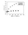
図8は、最初に実行されたエッチングにおけるE/Rを基準としたE/Rの変化の割合の一例を示す図である。[Process stability]
FIG. 8 is a diagram showing an example of the rate of change of E/R based on the E/R in the first etching performed.
チャンバ10内の部品の表面に保護膜が形成されていない場合、エッチングが実行されると、プラズマによりチャンバ10内の部品がダメージを受ける。これにより、チャンバ10内の部品が消耗し、チャンバ10内の環境が徐々に変化する。また、消耗した部品から発生したパーティクルが他の部品に付着し、電気的な特性を変化させる。そのため、最初に実行されたエッチングにおけるE/Rを基準とした場合、エッチングの累積時間が長くなるほどE/Rが徐々に変化してしまう。図7の例では、エッチングの累積時間が400[min]におけるE/Rは、最初に実行されたエッチングにおけるE/Rから40%以上変化している。If no protective film is formed on the surfaces of the components in the
これに対しチャンバ10内の部品の表面に保護膜が形成されている場合、エッチングが実行されても、チャンバ10内の部品はプラズマによるダメージを受け難い。これにより、チャンバ10内の部品の消耗が抑制され、チャンバ10内の環境の変化が抑制される。また、チャンバ10内の部品の消耗が抑制されるため、チャンバ10内の部品から発生するパーティクルも抑制され、チャンバ10内の部品の電気的な特性の変化が抑制される。そのため、最初に実行されたエッチングにおけるE/Rを基準とした場合、エッチングの累積時間が長くなってもE/Rの変化が抑制されている。図7の例では、エッチングの累積時間が400[min]において、E/Rの変化量は、最初に実行されたエッチングにおけるE/Rから6%程度に抑制されている。In contrast, if a protective film is formed on the surface of the parts in the
以上、一実施形態について説明した。上記したように、本実施形態におけるプラズマ処理方法は、基板Wをプラズマ処理するプラズマ処理方法であって、チャンバ10内において炭素および水素を含有する第1のガスをプラズマ化することにより、チャンバ10内の部品の表面を導電性を有する保護膜でコーティングする工程と、チャンバ10内に基板Wを搬入する工程と、チャンバ10内の部品の表面が導電性を有する保護膜でコーティングされた状態で、チャンバ10内において第2のガスをプラズマ化することにより、基板Wを処理する工程とを含む。これにより、チャンバ10内の部品の消耗を抑えつつ、プロセスの安定化を実現することができる。One embodiment has been described above. As described above, the plasma processing method in this embodiment is a plasma processing method for plasma processing a substrate W, and includes a step of coating the surfaces of components in the
また、上記した実施形態におけるコーティングする工程において、導電性を有する保護膜は、20[nm]以上の厚さでチャンバ10内の部品の表面に形成される。これにより、プラズマに含まれるイオン等によるチャンバ10内の部品へのダメージを抑制することができる。In addition, in the coating process in the above embodiment, a conductive protective film is formed on the surface of the components in the
また、上記した実施形態におけるプラズマ処理方法には、処理する工程の後に、チャンバ10内において酸素を含有する第3のガスをプラズマ化することにより、導電性を有する保護膜を除去する工程をさらに含む。また、除去する工程が実行された後、コーティングする工程が再び実行され、その後に前記処理する工程が実行される。これにより、保護膜上に堆積した反応副生成物を除去することができると共に、ダメージを受けた保護膜を除去し、新たな保護膜をチャンバ10内の部品の表面に形成することができる。The plasma processing method in the above embodiment further includes a step of removing the conductive protective film by converting a third gas containing oxygen into plasma in the
また、上記した実施形態において、第1のガスは、ハイドロカーボンガス、ハイドロフルオロカーボン、フルオロカーボンガスと水素を含有するガスとの混合ガス、または、ハイドロフルオロカーボンガスと水素を含有するガスとの混合ガスを含む。水素を含有するガスは、水素ガス、ハイドロカーボンガス、またはハイドロフルオロカーボンガスを含む。これにより、チャンバ10内の部品の表面を導電性を有する保護膜でコーティングすることができる。In the above-described embodiment, the first gas includes a hydrocarbon gas, a hydrofluorocarbon, a mixed gas of a fluorocarbon gas and a gas containing hydrogen, or a mixed gas of a hydrofluorocarbon gas and a gas containing hydrogen. The gas containing hydrogen includes hydrogen gas, a hydrocarbon gas, or a hydrofluorocarbon gas. This allows the surfaces of the components in the
また、上記した実施形態において、第2のガスには、フルオロカーボンガスが含まれる。第2のガスには、C4F6ガス、C4F8ガス、およびC5F8ガスのうち、少なくとも1つが含まれてもよい。また、第2のガスには、水素を含有するガスが含まれる。水素を含有するガスには、水素ガス、ハイドロカーボンガスまたはハイドロフルオロカーボンガスが含まれる。これにより、導電性を有する保護膜が形成されたチャンバ10内の部品の表面に導電性の反応副生成物が堆積し、チャンバ10内の環境の変化が抑制される。そのため、プロセスの安定化を実現することができる。 In the above embodiment,the second gas includes afluorocarbon gas. The second gas may include at least one ofC4F6 gas,C4F8 gas, andC5F8 gas. The second gas includes a gas containing hydrogen. The gas containing hydrogen includeshydrogen gas, a hydrocarbon gas, or a hydrofluorocarbon gas. This causes conductive reaction by-products to be deposited on the surfaces of the components in the
[その他]
なお、本願に開示された技術は、上記した実施形態に限定されるものではなく、その要旨の範囲内で数々の変形が可能である。[others]
The technology disclosed in the present application is not limited to the above-described embodiment, and various modifications are possible within the scope of the gist of the invention.
例えば、上記した各実施形態では、プラズマ源の一例として、容量結合型プラズマ(CCP)を用いて処理を行うプラズマ処理装置1として説明したが、プラズマ源はこれに限られない。容量結合型プラズマ以外のプラズマ源としては、例えば、誘導結合プラズマ(ICP)、マイクロ波励起表面波プラズマ(SWP)、電子サイクロトン共鳴プラズマ(ECP)、およびヘリコン波励起プラズマ(HWP)等が挙げられる。For example, in each of the above-described embodiments, the
なお、今回開示された実施形態は全ての点で例示であって制限的なものではないと考えられるべきである。実に、上記した実施形態は多様な形態で具現され得る。また、上記の実施形態は、添付の特許請求の範囲およびその趣旨を逸脱することなく、様々な形態で省略、置換、変更されてもよい。The disclosed embodiments should be considered in all respects as illustrative and not restrictive. Indeed, the above-described embodiments may be embodied in various forms. Furthermore, the above-described embodiments may be omitted, substituted, or modified in various forms without departing from the scope and spirit of the appended claims.
W 基板
1 プラズマ処理装置
10 チャンバ
10e 排気口
10s 処理空間
11 支持部
100 デポシールド
101 バッフル板側壁
102 バッフル板
103 リングシールド
111 下部電極
112 静電チャック
113 エッジリング
12 上部電極シャワーヘッドアセンブリ
12a ガス入口
12b ガス拡散室
12c ガス出口
20 ガス供給部
21 ガスソース
22 流量制御器
30 RF電力供給部
30a 第1のRF電力供給部
30b 第2のRF電力供給部
31a 第1のRF生成部
31b 第2のRF生成部
32a 第1の整合回路
32b 第2の整合回路
40 排気システム
50 制御部
51 コンピュータ
511 処理部
512 記憶部
513 通信インターフェイスW,
Claims (15)
Translated fromJapaneseチャンバ内において炭素および水素を含有する第1のガスをプラズマ化することにより、前記チャンバ内の部品の表面を20[nm]以上の厚さの導電性を有する膜でコーティングする工程と、
前記チャンバ内の支持部上に基板を配置する工程であり、前記支持部は下部電極を含む、工程と、
前記チャンバ内の部品の表面が前記導電性を有する膜でコーティングされた状態で、前記下部電極にプラズマ生成用の第1のRF電力を供給し、前記チャンバ内において第2のガスをプラズマ化することにより、前記基板を処理する工程と、
前記処理する工程の後に、前記チャンバ内において酸素を含有する第3のガスをプラズマ化することにより、前記導電性を有する膜を除去する工程と
を含み、
前記除去する工程が実行された後、前記コーティングする工程が再び実行された後、前記処理する工程が実行されるプラズマ処理方法。 1. A plasma processing method for plasma processing a substrate, comprising:
a step of forming a plasma of a first gas containing carbon and hydrogen in a chamber, thereby coating a surface of a component in the chamber with a conductive film having a thickness of 20 nm or more;
placinga substrate on a support within the chamber, the support including a bottom electrode;
a step of processing the substrate by supplying a first RF power for plasma generation to the lower electrode and generating plasma from a second gas in the chamber while the surface of a component in the chamber is coated with the conductive film;
and removing the conductive film by generating a third gas containing oxygen in the chamber as a plasma after the processing step,
A plasma processing method in which the removing step is performed, the coating step is performed again, and then the processing step is performed.
ハイドロカーボンガス、ハイドロフルオロカーボンガス、フルオロカーボンガスと水素を含有する第1の水素含有ガスとの混合ガス、または、ハイドロフルオロカーボンガスと前記第1の水素含有ガスとの混合ガスを含む請求項1に記載のプラズマ処理方法。 The first gas is
2. The plasma processing method according to claim 1, comprising a mixed gasof a hydrocarbon gas, a hydrofluorocarbon gas, a fluorocarbon gas anda first hydrogen-containing gas containing hydrogen, or a mixed gas of a hydrofluorocarbon gas and the first hydrogen-containing gas.
前記クリーニングする工程の後に、前記チャンバから前記ダミーウェハを搬出する工程をさらに含む請求項8に記載のプラズマ処理方法。 before the cleaning step, loading a dummy wafer into the chamber;
9. The plasma processing method according to claim 8, further comprising the step of unloading the dummy wafer from the chamber after the cleaning step.
前記チャンバ内で基板を支持するための支持部であって、下部電極を含む、支持部と、
前記下部電極に対向して配置される上部電極と、
前記第1のRF電力を供給するように構成された第1のRF生成部と、
前記プラズマ中のイオンを前記基板に引き込むための第2のRF電力を供給するように構成された第2のRF生成部と
を備えるプラズマ処理装置を用いて実行される、請求項1から9のいずれか一項に記載のプラズマ処理方法。 A chamber;
a support for supporting a substrate within the chamber,the support including a lower electrode;
an upper electrode disposed opposite the lower electrode;
a first RF generator configured to provide the first RFpower ;
10. The plasma processing method according to claim 1, wherein the plasma processing method is performed using a plasma processing apparatus including a second RF generating unit configured to supply a second RFpower to attract ions in the plasma to the substrate.
前記チャンバ内で基板を支持するための支持部であって、下部電極を含む、支持部と、
前記下部電極に対向して配置される上部電極と、
前記第1のRF電力を供給するように構成された第1のRF生成部と、
前記プラズマ中のイオンを前記基板に引き込むためのDCパルスを生成するように構成されたDCパルス生成部と
を含むプラズマ処理装置を用いて実行される、請求項1から9のいずれか一項に記載のプラズマ処理方法。 A chamber;
a support for supporting a substrate within the chamber,the support including a lower electrode;
an upper electrode disposed opposite the lower electrode;
a first RF generator configured to provide the first RFpower ;
and a DC pulse generating unit configured to generate a DC pulse for attracting ions in the plasma to the substrate.
前記チャンバ内で基板を支持するための支持部であって、下部電極を含む、支持部と、
前記下部電極に対向して配置される上部電極と、
プラズマ生成用の第1のRF電力を生成する第1のRF生成部と、
バイアス用の第2のRF電力を生成する第2のRF生成部又はバイアス用のDCパルスを生成するDCパルス生成部と、
制御部と、
を含み、
前記制御部は、
チャンバ内において炭素および水素を含有する第1のガスをプラズマ化することにより、前記チャンバ内の部品の表面を20[nm]以上の厚さの導電性を有する膜でコーティングする工程と、
前記支持部上に前記基板を配置する工程と、
前記チャンバ内の部品の表面が前記導電性を有する膜でコーティングされた状態で、前記下部電極に前記第1のRF電力を供給し、前記チャンバ内において第2のガスをプラズマ化することにより、前記基板を処理する工程と、
前記処理する工程の後に、前記チャンバ内において酸素を含有する第3のガスをプラズマ化することにより、前記導電性を有する膜を除去する工程と
を実行するように構成され、
前記除去する工程が実行された後、前記コーティングする工程が再び実行された後、前記処理する工程が実行される、プラズマ処理装置。 A chamber;
a support for supporting a substrate within the chamber,the support including a lower electrode;
an upper electrode disposed opposite the lower electrode;
afirst RF generating unit that generates a first RF power forgenerating plasma ;
A second RF generating unitthat generates a second RF power for biasing ora DC pulse generating unit that generates a DC pulse for biasing ;
A control unit;
Including,
The control unit is
a step of forming a plasma of a first gas containing carbon and hydrogen in a chamber, thereby coating a surface of a component in the chamber with a conductive film having a thickness of 20 nm or more;
placing the substrateon the support ;
a step ofprocessing the substrate by supplying the first RF power to the lower electrode and generating plasma of a second gas in the chamber while a surface of a component in the chamber is coated with the conductive film;
a step of removing the conductive film by generating a third gas containing oxygen in the chamber as plasma after the processing step,
A plasma processing apparatus, wherein after the removing step is performed, the coating step is performed again, and then the processing step is performed.
前記チャンバ内で基板を支持する支持部であって、下部電極を含む支持部と、a support for supporting a substrate within the chamber, the support including a lower electrode;
前記下部電極に対向して配置される上部電極と、an upper electrode disposed opposite the lower electrode;
プラズマ生成用の第1のRF電力を生成する第1のRF生成部と、a first RF generating unit that generates a first RF power for generating plasma;
バイアス用の第2のRF電力を生成する第2のRF生成部又はバイアス用のDCパルスを生成するDCパルス生成部と、A second RF generating unit that generates a second RF power for biasing or a DC pulse generating unit that generates a DC pulse for biasing;
制御部と、A control unit;
を含み、Including,
前記制御部は、The control unit is
チャンバ内において炭素および水素を含有する第1のガスをプラズマ化することにより、前記チャンバ内の部品の表面を導電性を有する膜でコーティングする工程と、A step of forming a plasma of a first gas containing carbon and hydrogen in a chamber to coat a surface of a component in the chamber with a conductive film;
前記チャンバ内に前記基板を配置する工程と、placing the substrate in the chamber;
前記チャンバ内の部品の表面が前記導電性を有する膜でコーティングされた状態で、前記下部電極に前記第1のRF電力を供給し、前記チャンバ内において第2のガスをプラズマ化することにより、前記基板を処理する工程と、a step of processing the substrate by supplying the first RF power to the lower electrode and generating plasma of a second gas in the chamber while a surface of a component in the chamber is coated with the conductive film;
を実行するように構成される、プラズマ処理装置。The plasma processing apparatus is configured to perform the steps of:
Priority Applications (5)
| Application Number | Priority Date | Filing Date | Title |
|---|---|---|---|
| JP2020029071AJP7529412B2 (en) | 2020-02-25 | 2020-02-25 | Plasma processing method and plasma processing apparatus |
| CN202110189883.5ACN113380599B (en) | 2020-02-25 | 2021-02-18 | Plasma treatment method |
| KR1020210023298AKR20210108322A (en) | 2020-02-25 | 2021-02-22 | Plasma processing method |
| US17/182,896US11749508B2 (en) | 2020-02-25 | 2021-02-23 | Plasma processing method |
| US18/220,403US12080521B2 (en) | 2020-02-25 | 2023-07-11 | Plasma processing method |
Applications Claiming Priority (1)
| Application Number | Priority Date | Filing Date | Title |
|---|---|---|---|
| JP2020029071AJP7529412B2 (en) | 2020-02-25 | 2020-02-25 | Plasma processing method and plasma processing apparatus |
Publications (2)
| Publication Number | Publication Date |
|---|---|
| JP2021136255A JP2021136255A (en) | 2021-09-13 |
| JP7529412B2true JP7529412B2 (en) | 2024-08-06 |
Family
ID=77366365
Family Applications (1)
| Application Number | Title | Priority Date | Filing Date |
|---|---|---|---|
| JP2020029071AActiveJP7529412B2 (en) | 2020-02-25 | 2020-02-25 | Plasma processing method and plasma processing apparatus |
Country Status (4)
| Country | Link |
|---|---|
| US (2) | US11749508B2 (en) |
| JP (1) | JP7529412B2 (en) |
| KR (1) | KR20210108322A (en) |
| CN (1) | CN113380599B (en) |
Families Citing this family (3)
| Publication number | Priority date | Publication date | Assignee | Title |
|---|---|---|---|---|
| KR102810078B1 (en)* | 2021-12-22 | 2025-05-21 | 도쿄엘렉트론가부시키가이샤 | Maintenance method of substrate processing device and substrate processing device |
| KR20250091324A (en)* | 2022-08-26 | 2025-06-20 | 도쿄엘렉트론가부시키가이샤 | Etching method, precoating method and etching apparatus |
| WO2025013581A1 (en)* | 2023-07-07 | 2025-01-16 | 東京エレクトロン株式会社 | Plasma treatment method and plasma treatment device |
Citations (4)
| Publication number | Priority date | Publication date | Assignee | Title |
|---|---|---|---|---|
| JP2006165093A (en) | 2004-12-03 | 2006-06-22 | Tokyo Electron Ltd | Plasma processing device |
| JP2009188257A (en) | 2008-02-07 | 2009-08-20 | Tokyo Electron Ltd | Plasma etching method, plasma etching apparatus, and storage medium |
| JP2016076515A (en) | 2014-10-02 | 2016-05-12 | 株式会社東芝 | Manufacturing method of semiconductor device |
| JP2018133483A (en) | 2017-02-16 | 2018-08-23 | 東京エレクトロン株式会社 | Plasma processing method and plasma processing apparatus |
Family Cites Families (28)
| Publication number | Priority date | Publication date | Assignee | Title |
|---|---|---|---|---|
| US5085727A (en)* | 1990-05-21 | 1992-02-04 | Applied Materials, Inc. | Plasma etch apparatus with conductive coating on inner metal surfaces of chamber to provide protection from chemical corrosion |
| US5846332A (en)* | 1996-07-12 | 1998-12-08 | Applied Materials, Inc. | Thermally floating pedestal collar in a chemical vapor deposition chamber |
| US5993916A (en)* | 1996-07-12 | 1999-11-30 | Applied Materials, Inc. | Method for substrate processing with improved throughput and yield |
| JP2904163B2 (en)* | 1996-12-11 | 1999-06-14 | 日本電気株式会社 | Method for manufacturing semiconductor device |
| US5834371A (en)* | 1997-01-31 | 1998-11-10 | Tokyo Electron Limited | Method and apparatus for preparing and metallizing high aspect ratio silicon semiconductor device contacts to reduce the resistivity thereof |
| KR100269649B1 (en)* | 1998-08-28 | 2000-10-16 | 조장연 | Design of inductively coupled plasma etcher and etching process for gan semiconductor thin solid film |
| JP4168126B2 (en)* | 2000-11-16 | 2008-10-22 | 東京エレクトロン株式会社 | Method for stabilizing the inner surface of a plasma enhanced chemical vapor deposition chamber |
| JP2002164328A (en)* | 2000-11-27 | 2002-06-07 | Seiko Epson Corp | Dry etching equipment |
| US6887521B2 (en)* | 2002-08-15 | 2005-05-03 | Micron Technology, Inc. | Gas delivery system for pulsed-type deposition processes used in the manufacturing of micro-devices |
| JP4256763B2 (en)* | 2003-11-19 | 2009-04-22 | 東京エレクトロン株式会社 | Plasma processing method and plasma processing apparatus |
| JP4550507B2 (en)* | 2004-07-26 | 2010-09-22 | 株式会社日立ハイテクノロジーズ | Plasma processing equipment |
| US8177990B2 (en)* | 2006-03-31 | 2012-05-15 | Tokyo Electron Limited | Etching method, plasma processing system and storage medium |
| US20080178805A1 (en)* | 2006-12-05 | 2008-07-31 | Applied Materials, Inc. | Mid-chamber gas distribution plate, tuned plasma flow control grid and electrode |
| KR101399608B1 (en)* | 2007-07-27 | 2014-05-26 | 가부시키가이샤 한도오따이 에네루기 켄큐쇼 | Method for manufacturing semiconductor device |
| US20100043821A1 (en)* | 2008-08-19 | 2010-02-25 | Li Siyi | method of photoresist removal in the presence of a low-k dielectric layer |
| WO2011055856A1 (en)* | 2009-11-05 | 2011-05-12 | 住友金属鉱山株式会社 | Transparent conductive film and manufacturing method for same, element using same, transparent conductive substrate and device using same |
| KR20130095119A (en)* | 2012-02-17 | 2013-08-27 | 김일욱 | Atomospheric pressure plasma generating apparatus |
| CN103794460B (en)* | 2012-10-29 | 2016-12-21 | 中微半导体设备(上海)有限公司 | The coating improved for performance of semiconductor devices |
| US20140186544A1 (en)* | 2013-01-02 | 2014-07-03 | Applied Materials, Inc. | Metal processing using high density plasma |
| US20140315392A1 (en)* | 2013-04-22 | 2014-10-23 | Lam Research Corporation | Cold spray barrier coated component of a plasma processing chamber and method of manufacture thereof |
| JP6422262B2 (en)* | 2013-10-24 | 2018-11-14 | 東京エレクトロン株式会社 | Plasma processing method and plasma processing apparatus |
| US20150311043A1 (en)* | 2014-04-25 | 2015-10-29 | Applied Materials, Inc. | Chamber component with fluorinated thin film coating |
| JP2016086046A (en) | 2014-10-24 | 2016-05-19 | 東京エレクトロン株式会社 | Plasma processing method |
| US9928994B2 (en)* | 2015-02-03 | 2018-03-27 | Lam Research Corporation | Methods for decreasing carbon-hydrogen content of amorphous carbon hardmask films |
| US11694911B2 (en)* | 2016-12-20 | 2023-07-04 | Lam Research Corporation | Systems and methods for metastable activated radical selective strip and etch using dual plenum showerhead |
| JP6925202B2 (en)* | 2017-08-30 | 2021-08-25 | 東京エレクトロン株式会社 | Etching method and etching equipment |
| JP6799549B2 (en)* | 2018-01-16 | 2020-12-16 | 東京エレクトロン株式会社 | How to clean parts of plasma processing equipment |
| WO2021146098A1 (en)* | 2020-01-13 | 2021-07-22 | Lam Research Corporation | Mixed metal baseplates for improved thermal expansion matching with thermal oxide spraycoat |
- 2020
- 2020-02-25JPJP2020029071Apatent/JP7529412B2/enactiveActive
- 2021
- 2021-02-18CNCN202110189883.5Apatent/CN113380599B/enactiveActive
- 2021-02-22KRKR1020210023298Apatent/KR20210108322A/ennot_activeCeased
- 2021-02-23USUS17/182,896patent/US11749508B2/enactiveActive
- 2023
- 2023-07-11USUS18/220,403patent/US12080521B2/enactiveActive
Patent Citations (4)
| Publication number | Priority date | Publication date | Assignee | Title |
|---|---|---|---|---|
| JP2006165093A (en) | 2004-12-03 | 2006-06-22 | Tokyo Electron Ltd | Plasma processing device |
| JP2009188257A (en) | 2008-02-07 | 2009-08-20 | Tokyo Electron Ltd | Plasma etching method, plasma etching apparatus, and storage medium |
| JP2016076515A (en) | 2014-10-02 | 2016-05-12 | 株式会社東芝 | Manufacturing method of semiconductor device |
| JP2018133483A (en) | 2017-02-16 | 2018-08-23 | 東京エレクトロン株式会社 | Plasma processing method and plasma processing apparatus |
Also Published As
| Publication number | Publication date |
|---|---|
| US11749508B2 (en) | 2023-09-05 |
| US20230360891A1 (en) | 2023-11-09 |
| US12080521B2 (en) | 2024-09-03 |
| CN113380599A (en) | 2021-09-10 |
| CN113380599B (en) | 2025-09-23 |
| KR20210108322A (en) | 2021-09-02 |
| US20210265135A1 (en) | 2021-08-26 |
| JP2021136255A (en) | 2021-09-13 |
Similar Documents
| Publication | Publication Date | Title |
|---|---|---|
| JP5390846B2 (en) | Plasma etching apparatus and plasma cleaning method | |
| KR100891754B1 (en) | Method for cleaning substrate processing chamber, storage medium and substrate processing chamber | |
| JP5281309B2 (en) | Plasma etching apparatus, plasma etching method, and computer-readable storage medium | |
| US12080521B2 (en) | Plasma processing method | |
| US9852922B2 (en) | Plasma processing method | |
| JP2007180358A (en) | Plasma etching method and computer-readable recording medium | |
| US10553409B2 (en) | Method of cleaning plasma processing apparatus | |
| US10957515B2 (en) | Plasma processing method and plasma processing apparatus | |
| US9653317B2 (en) | Plasma processing method and plasma processing apparatus | |
| WO2014034396A1 (en) | Plasma processing method and plasma processing device | |
| JP2016207772A (en) | Method for etching an organic film | |
| TWI743123B (en) | Plasma processing method | |
| JP2016086046A (en) | Plasma processing method | |
| US10651077B2 (en) | Etching method | |
| EP2980829B1 (en) | Plasma processing apparatus and plasma processing method | |
| US11721595B2 (en) | Processing method and plasma processing apparatus | |
| CN113284786A (en) | Substrate processing method and substrate processing apparatus | |
| US20200144051A1 (en) | Processing method and substrate processing apparatus | |
| US12300467B2 (en) | Plasma processing method and plasma processing apparatus | |
| US20230086580A1 (en) | Etching method and plasma processing apparatus | |
| WO2025013581A1 (en) | Plasma treatment method and plasma treatment device | |
| WO2025204284A1 (en) | Plasma processing apparatus and plasma processing method | |
| JP2023018631A (en) | Etching method, semiconductor device manufacturing method, program, and plasma processing apparatus | |
| JP2015106587A (en) | Method for coating electrostatic chuck and plasma processing apparatus |
Legal Events
| Date | Code | Title | Description |
|---|---|---|---|
| A621 | Written request for application examination | Free format text:JAPANESE INTERMEDIATE CODE: A621 Effective date:20221111 | |
| A977 | Report on retrieval | Free format text:JAPANESE INTERMEDIATE CODE: A971007 Effective date:20230831 | |
| A131 | Notification of reasons for refusal | Free format text:JAPANESE INTERMEDIATE CODE: A131 Effective date:20230905 | |
| A521 | Request for written amendment filed | Free format text:JAPANESE INTERMEDIATE CODE: A523 Effective date:20231106 | |
| A131 | Notification of reasons for refusal | Free format text:JAPANESE INTERMEDIATE CODE: A131 Effective date:20240123 | |
| A521 | Request for written amendment filed | Free format text:JAPANESE INTERMEDIATE CODE: A523 Effective date:20240325 | |
| TRDD | Decision of grant or rejection written | ||
| A01 | Written decision to grant a patent or to grant a registration (utility model) | Free format text:JAPANESE INTERMEDIATE CODE: A01 Effective date:20240625 | |
| A61 | First payment of annual fees (during grant procedure) | Free format text:JAPANESE INTERMEDIATE CODE: A61 Effective date:20240725 | |
| R150 | Certificate of patent or registration of utility model | Ref document number:7529412 Country of ref document:JP Free format text:JAPANESE INTERMEDIATE CODE: R150 |