JP7528163B2 - Semiconductor Device - Google Patents
Semiconductor DeviceDownload PDFInfo
- Publication number
- JP7528163B2 JP7528163B2JP2022143530AJP2022143530AJP7528163B2JP 7528163 B2JP7528163 B2JP 7528163B2JP 2022143530 AJP2022143530 AJP 2022143530AJP 2022143530 AJP2022143530 AJP 2022143530AJP 7528163 B2JP7528163 B2JP 7528163B2
- Authority
- JP
- Japan
- Prior art keywords
- transistor
- oxide semiconductor
- semiconductor
- insulator
- region
- Prior art date
- Legal status (The legal status is an assumption and is not a legal conclusion. Google has not performed a legal analysis and makes no representation as to the accuracy of the status listed.)
- Active
Links
Images


Classifications
- H—ELECTRICITY
- H10—SEMICONDUCTOR DEVICES; ELECTRIC SOLID-STATE DEVICES NOT OTHERWISE PROVIDED FOR
- H10D—INORGANIC ELECTRIC SEMICONDUCTOR DEVICES
- H10D30/00—Field-effect transistors [FET]
- H10D30/60—Insulated-gate field-effect transistors [IGFET]
- H10D30/67—Thin-film transistors [TFT]
- H10D30/674—Thin-film transistors [TFT] characterised by the active materials
- H10D30/6755—Oxide semiconductors, e.g. zinc oxide, copper aluminium oxide or cadmium stannate
- H—ELECTRICITY
- H10—SEMICONDUCTOR DEVICES; ELECTRIC SOLID-STATE DEVICES NOT OTHERWISE PROVIDED FOR
- H10D—INORGANIC ELECTRIC SEMICONDUCTOR DEVICES
- H10D30/00—Field-effect transistors [FET]
- H10D30/60—Insulated-gate field-effect transistors [IGFET]
- H10D30/67—Thin-film transistors [TFT]
- H10D30/6729—Thin-film transistors [TFT] characterised by the electrodes
- H10D30/673—Thin-film transistors [TFT] characterised by the electrodes characterised by the shapes, relative sizes or dispositions of the gate electrodes
- H10D30/6733—Multi-gate TFTs
- H10D30/6734—Multi-gate TFTs having gate electrodes arranged on both top and bottom sides of the channel, e.g. dual-gate TFTs
- H—ELECTRICITY
- H10—SEMICONDUCTOR DEVICES; ELECTRIC SOLID-STATE DEVICES NOT OTHERWISE PROVIDED FOR
- H10D—INORGANIC ELECTRIC SEMICONDUCTOR DEVICES
- H10D30/00—Field-effect transistors [FET]
- H10D30/60—Insulated-gate field-effect transistors [IGFET]
- H10D30/67—Thin-film transistors [TFT]
- H10D30/6757—Thin-film transistors [TFT] characterised by the structure of the channel, e.g. transverse or longitudinal shape or doping profile
Landscapes
- Thin Film Transistor (AREA)
- Semiconductor Memories (AREA)
- Metal-Oxide And Bipolar Metal-Oxide Semiconductor Integrated Circuits (AREA)
Description
Translated fromJapanese本発明は、物、方法、または、製造方法に関する。または、本発明は、プロセス、マシン
、マニュファクチャ、または組成物(コンポジション・オブ・マター)に関する。特に、
本発明は、例えば、半導体、半導体装置、表示装置、発光装置、照明装置、蓄電装置、記
憶装置またはプロセッサに関する。または、半導体、半導体装置、表示装置、発光装置、
照明装置、蓄電装置、記憶装置またはプロセッサの製造方法に関する。または、半導体装
置、表示装置、発光装置、照明装置、蓄電装置、記憶装置またはプロセッサの駆動方法に
関する。The present invention relates to an object, a method, or a manufacturing method, or the present invention relates to a process, a machine, a manufacture, or a composition of matter.
The present invention relates to, for example, a semiconductor device, a display device, a light-emitting device, a lighting device, a power storage device, a storage device, or a processor.
The present invention relates to a method for manufacturing a lighting device, a power storage device, a memory device, or a processor, or to a method for driving a semiconductor device, a display device, a light-emitting device, a lighting device, a power storage device, a memory device, or a processor.
なお、本明細書などにおいて半導体装置とは、半導体特性を利用することで機能しうる装
置全般を指す。表示装置、発光装置、照明装置、電気光学装置、半導体回路および電子機
器は、半導体装置を有する場合がある。In this specification and the like, the term "semiconductor device" refers to any device that can function by utilizing semiconductor characteristics. Display devices, light-emitting devices, lighting devices, electro-optical devices, semiconductor circuits, and electronic devices may include semiconductor devices.
絶縁表面を有する基板上に形成された半導体薄膜を用いてトランジスタを構成する技術が
注目されている。当該トランジスタは集積回路(IC)や画像表示装置(単に表示装置と
も表記する)のような電子デバイスに広く応用されている。トランジスタに適用可能な半
導体薄膜として、シリコン系半導体材料が広く知られているが、その他の材料として酸化
物半導体が注目されている。A technology for constructing a transistor using a semiconductor thin film formed on a substrate having an insulating surface has been attracting attention. The transistor is widely applied to electronic devices such as integrated circuits (ICs) and image display devices (also simply referred to as display devices). Silicon-based semiconductor materials are widely known as semiconductor thin films that can be applied to transistors, but oxide semiconductors have also attracted attention as other materials.
例えば、酸化亜鉛、またはIn-Ga-Zn酸化物半導体を用いてトランジスタを作製す
る技術が開示されている(特許文献1および特許文献2参照)。For example, techniques for manufacturing a transistor using zinc oxide or an In--Ga--Zn oxide semiconductor have been disclosed (see
また、c軸に配向した結晶構造を持つ酸化物半導体をトランジスタの活性層として用いた
高精細・低消費電力の表示装置が開示されている(非特許文献1参照)。Also, a high-definition, low-power consumption display device has been disclosed that uses an oxide semiconductor having a crystal structure oriented along the c-axis as an active layer of a transistor (see Non-Patent Document 1).
また、近年では電子機器の高性能化、小型化、または軽量化に伴い、微細化されたトラン
ジスタなどの半導体素子を高密度に集積した集積回路の要求が高まっている。Furthermore, in recent years, with the trend toward higher performance, smaller size, and lighter weight of electronic devices, there has been an increasing demand for integrated circuits in which semiconductor elements such as miniaturized transistors are densely integrated.
例えば、c軸が表面に垂直な方向に配向した結晶構造を持つ酸化物半導体を活性層として
用いたトランジスタは極めて低いオフ電流を持ち(非特許文献2参照)、その特性を利用
した不揮発性メモリ、CPU、イメージセンサなどのLSIへの応用が提案されている(
非特許文献3乃至非特許文献5参照)。For example, a transistor using an oxide semiconductor having a crystal structure in which the c-axis is oriented perpendicular to the surface as an active layer has an extremely low off-state current (see Non-Patent Document 2), and its application to LSIs such as non-volatile memories, CPUs, and image sensors utilizing this characteristic has been proposed (
(See Non-Patent
良好な電気特性を有するトランジスタを提供することを課題の一つとする。または、微細
化に適したトランジスタを提供することを課題の一つとする。または、スイッチングスピ
ードの速いトランジスタを提供することを課題の一つとする。または、導通時の電流の大
きいトランジスタを提供することを課題の一とする。または、当該トランジスタを有する
半導体装置を提供することを課題の一とする。または、当該トランジスタを有する動作速
度の速い半導体装置を提供することを課題の一とする。An object of the present invention is to provide a transistor having good electrical characteristics. Another object of the present invention is to provide a transistor suitable for miniaturization. Another object of the present invention is to provide a transistor with a high switching speed. Another object of the present invention is to provide a transistor with a large current when conducting. Another object of the present invention is to provide a semiconductor device including the transistor. Another object of the present invention is to provide a semiconductor device including the transistor and having a high operating speed.
なお、これらの課題の記載は、他の課題の存在を妨げるものではない。なお、本発明の一
態様は、これらの課題の全てを解決する必要はないものとする。なお、これら以外の課題
は、明細書、図面、請求項などの記載から、自ずと明らかとなるものであり、明細書、図
面、請求項などの記載から、これら以外の課題を抽出することが可能である。Note that the description of these problems does not preclude the existence of other problems. Note that one embodiment of the present invention does not necessarily solve all of these problems. Note that problems other than these will become apparent from the description of the specification, drawings, claims, etc., and it is possible to extract problems other than these from the description of the specification, drawings, claims, etc.
本発明の一態様は、酸化物半導体と、ゲート電極と、ゲート絶縁体と、を有するトランジ
スタを有し、前記酸化物半導体は、前記ゲート絶縁体を介して前記酸化物半導体と、前記
ゲート電極と、が互いに重なる第1の領域を有し、前記トランジスタは、しきい値電圧が
0Vより大きく、かつスイッチ速度が100ナノ秒未満である半導体装置である。One embodiment of the present invention is a semiconductor device that includes a transistor having an oxide semiconductor, a gate electrode, and a gate insulator, the oxide semiconductor having a first region where the oxide semiconductor and the gate electrode overlap with each other via the gate insulator, and the transistor has a threshold voltage higher than 0 V and a switching speed of less than 100 nanoseconds.
または、本発明の一態様は、ゲート電極にしきい値電圧以上の電圧を印加したとき、前記
酸化物半導体の全体を電流が流れる半導体装置である。Another embodiment of the present invention is a semiconductor device in which a current flows through the entire oxide semiconductor when a voltage equal to or higher than the threshold voltage is applied to a gate electrode.
または、本発明の一態様は、第1の領域のキャリア密度が、1×1015cm-3未満で
ある半導体装置である。Another embodiment of the present invention is a semiconductor device in which the carrier density of the first region is less than 1×1015 cm−3 .
または、本発明の一態様は、酸化物半導体は、ゲート絶縁体を介して当該酸化物半導体の
側面と、前記ゲート電極と、が面する第2の領域を有する半導体装置である。Another embodiment of the present invention is a semiconductor device in which an oxide semiconductor has a second region in which a side surface of the oxide semiconductor faces the gate electrode with a gate insulator interposed therebetween.
または、本発明の一態様は、酸化物半導体と接する導電体を有し、酸化物半導体は、導電
体と接する第3の領域を有し、第3の領域は、酸素欠損のサイトを有し、酸素欠損のサイ
トは、水素を有する半導体装置である。Another embodiment of the present invention is a semiconductor device including a conductor in contact with an oxide semiconductor. The oxide semiconductor includes a third region in contact with the conductor. The third region has an oxygen vacancy site, and the oxygen vacancy site contains hydrogen.
または、本発明の一態様は、第3の領域はn型導電領域である半導体装置である。Alternatively, one aspect of the present invention is a semiconductor device in which the third region is an n-type conductive region.
良好な電気特性を有するトランジスタを提供することができる。または、微細化に適した
トランジスタを提供することができる。または、スイッチングスピードの速いトランジス
タを提供することができる。または、導通時の電流の大きいトランジスタを提供すること
ができる。または、当該トランジスタを有する半導体装置を提供することができる。また
は、当該トランジスタを有する動作速度の速い半導体装置を提供することができる。It is possible to provide a transistor having good electrical characteristics. Or, it is possible to provide a transistor suitable for miniaturization. Or, it is possible to provide a transistor with a high switching speed. Or, it is possible to provide a transistor with a large current when conducting. Or, it is possible to provide a semiconductor device including the transistor. Or, it is possible to provide a semiconductor device including the transistor and having a high operating speed.
本発明の実施の形態について、図面を用いて詳細に説明する。ただし、本発明は以下の説
明に限定されず、その形態および詳細を様々に変更し得ることは、当業者であれば容易に
理解される。また、本発明は以下に示す実施の形態の記載内容に限定して解釈されるもの
ではない。なお、図面を用いて発明の構成を説明するにあたり、同じものを指す符号は異
なる図面間でも共通して用いる。なお、同様のものを指す際にはハッチパターンを同じく
し、特に符号を付さない場合がある。The embodiments of the present invention will be described in detail with reference to the drawings. However, the present invention is not limited to the following description, and it will be easily understood by those skilled in the art that the form and details of the present invention can be modified in various ways. Furthermore, the present invention is not interpreted as being limited to the description of the embodiments shown below. Note that, when describing the configuration of the invention with reference to the drawings, symbols indicating the same objects are used in common between different drawings. Note that when indicating similar objects, the same hatch pattern may be used, and no particular symbol may be attached.
なお、図において、大きさ、膜(層)の厚さ、または領域は、明瞭化のために誇張されて
いる場合がある。In addition, in the figures, the size, thickness of the film (layer), or area may be exaggerated for clarity.
また、電圧は、ある電位と、基準の電位(例えば接地電位(GND)またはソース電位)
との電位差のことを示す場合が多い。よって、電圧を電位と言い換えることが可能である
。The voltage is a potential and a reference potential (for example, a ground potential (GND) or a source potential).
In many cases, it refers to the potential difference between the potential and the voltage. Therefore, it is possible to say "voltage" in other words "electric potential."
なお、第1、第2として付される序数詞は便宜的に用いるものであり、工程順または積層
順を示すものではない。そのため、例えば、「第1の」を「第2の」または「第3の」な
どと適宜置き換えて説明することができる。また、本明細書等に記載されている序数詞と
、本発明の一態様を特定するために用いられる序数詞は一致しない場合がある。Note that the ordinal numbers such as first and second are used for convenience and do not indicate the order of steps or stacking. Therefore, for example, "first" can be appropriately replaced with "second" or "third" for explanation. In addition, the ordinal numbers described in this specification and the like may not match the ordinal numbers used to specify one embodiment of the present invention.
なお、「半導体」と表記した場合でも、例えば、導電性が十分低い場合は「絶縁体」とし
ての特性を有する場合がある。また、「半導体」と「絶縁体」は境界が曖昧であり、厳密
に区別できない場合がある。したがって、本明細書に記載の「半導体」は、「絶縁体」と
言い換えることができる場合がある。同様に、本明細書に記載の「絶縁体」は、「半導体
」と言い換えることができる場合がある。Even when written as "semiconductor", for example, if the conductivity is sufficiently low, it may have the characteristics of an "insulator". In addition, the boundary between "semiconductor" and "insulator" is ambiguous, and they may not be strictly distinguishable. Therefore, the "semiconductor" described in this specification may be rephrased as "insulator". Similarly, the "insulator" described in this specification may be rephrased as "semiconductor".
また、「半導体」と表記した場合でも、例えば、導電性が十分高い場合は「導電体」とし
ての特性を有する場合がある。また、「半導体」と「導電体」は境界が曖昧であり、厳密
に区別できない場合がある。したがって、本明細書に記載の「半導体」は、「導電体」と
言い換えることができる場合がある。同様に、本明細書に記載の「導電体」は、「半導体
」と言い換えることができる場合がある。Even when written as "semiconductor", for example, if the conductivity is sufficiently high, it may have the characteristics of a "conductor". Furthermore, the boundary between "semiconductor" and "conductor" is ambiguous, and they may not be strictly distinguishable. Therefore, the "semiconductor" described in this specification may be rephrased as "conductor". Similarly, the "conductor" described in this specification may be rephrased as "semiconductor".
なお、半導体の不純物とは、例えば、半導体を構成する主成分以外をいう。例えば、濃度
が0.1原子%未満の元素は不純物である。不純物が含まれることにより、例えば、半導
体にDOS(Density of State)が形成されることや、キャリア移動度
が低下することや、結晶性が低下することなどが起こる場合がある。半導体が酸化物半導
体である場合、半導体の特性を変化させる不純物としては、例えば、第1族元素、第2族
元素、第14族元素、第15族元素、主成分以外の遷移金属などがあり、特に、例えば、
水素(水にも含まれる)、リチウム、ナトリウム、シリコン、ホウ素、リン、炭素、窒素
などがある。酸化物半導体の場合、例えば水素などの不純物の混入によって酸素欠損を形
成する場合がある。また、半導体がシリコンである場合、半導体の特性を変化させる不純
物としては、例えば、酸素、水素を除く第1族元素、第2族元素、第13族元素、第15
族元素などがある。Note that impurities in a semiconductor refer to, for example, elements other than the main components constituting the semiconductor. For example, an element with a concentration of less than 0.1 atomic % is an impurity. When an impurity is contained, for example, density of state (DOS) may be formed in the semiconductor, carrier mobility may be reduced, or crystallinity may be reduced. When the semiconductor is an oxide semiconductor, examples of impurities that change the characteristics of the semiconductor include
Examples of impurities that change the characteristics of a semiconductor include hydrogen (also contained in water), lithium, sodium, silicon, boron, phosphorus, carbon, and nitrogen. In the case of an oxide semiconductor, oxygen vacancies may be formed by the inclusion of impurities such as hydrogen. In addition, in the case of a silicon semiconductor, impurities that change the characteristics of a semiconductor include, for example, oxygen,
Group elements, etc.
なお、以下に示す実施の形態では、特に断りがない場合、絶縁体として、例えば、ホウ素
、炭素、窒素、酸素、フッ素、マグネシウム、アルミニウム、シリコン、リン、塩素、ア
ルゴン、ガリウム、ゲルマニウム、イットリウム、ジルコニウム、ランタン、ネオジム、
ハフニウムまたはタンタルを一種以上含む絶縁体を、単層で、または積層で用いればよい
。または、絶縁体として、樹脂を用いてもよい。例えば、ポリイミド、ポリアミド、アク
リル、シリコーンなどを含む樹脂を用いればよい。樹脂を用いることで、絶縁体の上面を
平坦化処理しなくてもよい場合がある。また、樹脂は短い時間で厚い膜を成膜することが
できるため、生産性を高めることができる。絶縁体としては、好ましくは酸化アルミニウ
ム、窒化酸化シリコン、窒化シリコン、酸化ガリウム、酸化イットリウム、酸化ジルコニ
ウム、酸化ランタン、酸化ネオジム、酸化ハフニウムまたは酸化タンタルを含む絶縁体を
、単層で、または積層で用いればよい。In the following embodiments, unless otherwise specified, examples of insulators include boron, carbon, nitrogen, oxygen, fluorine, magnesium, aluminum, silicon, phosphorus, chlorine, argon, gallium, germanium, yttrium, zirconium, lanthanum, neodymium,
An insulator containing one or more of hafnium or tantalum may be used in a single layer or a laminated layer. Alternatively, a resin may be used as the insulator. For example, a resin containing polyimide, polyamide, acrylic, silicone, or the like may be used. By using a resin, it may not be necessary to perform a planarization process on the upper surface of the insulator. In addition, since a thick film can be formed with the resin in a short time, productivity can be improved. As the insulator, an insulator containing aluminum oxide, silicon nitride oxide, silicon nitride, gallium oxide, yttrium oxide, zirconium oxide, lanthanum oxide, neodymium oxide, hafnium oxide, or tantalum oxide may be used in a single layer or a laminated layer.
また、以下に示す実施の形態では、特に断りがない場合、導電体として、例えば、ホウ素
、窒素、酸素、フッ素、シリコン、リン、アルミニウム、チタン、クロム、マンガン、コ
バルト、ニッケル、銅、亜鉛、ガリウム、イットリウム、ジルコニウム、モリブデン、ル
テニウム、銀、インジウム、スズ、タンタルまたはタングステンを一種以上含む導電体を
、単層で、または積層で用いればよい。例えば、合金や化合物であってもよく、アルミニ
ウムを含む導電体、銅およびチタンを含む導電体、銅およびマンガンを含む導電体、イン
ジウム、スズおよび酸素を含む導電体、チタンおよび窒素を含む導電体などを用いてもよ
い。In the embodiments described below, unless otherwise specified, the conductor may be, for example, a conductor containing one or more of boron, nitrogen, oxygen, fluorine, silicon, phosphorus, aluminum, titanium, chromium, manganese, cobalt, nickel, copper, zinc, gallium, yttrium, zirconium, molybdenum, ruthenium, silver, indium, tin, tantalum, or tungsten, in a single layer or a multilayer. For example, an alloy or compound may be used, and a conductor containing aluminum, a conductor containing copper and titanium, a conductor containing copper and manganese, a conductor containing indium, tin, and oxygen, a conductor containing titanium and nitrogen, or the like may be used.
なお、本明細書において、Aが濃度Bの領域を有する、と記載する場合、例えば、Aのあ
る領域における深さ方向全体が濃度Bである場合、Aのある領域における深さ方向の平均
値が濃度Bである場合、Aのある領域における深さ方向の中央値が濃度Bである場合、A
のある領域における深さ方向の最大値が濃度Bである場合、Aのある領域における深さ方
向の最小値が濃度Bである場合、Aのある領域における深さ方向の収束値が濃度Bである
場合、測定上Aそのものの確からしい値の得られる領域が濃度Bである場合などを含む。In this specification, when it is stated that A has a region of concentration B, for example, when the entire depth direction of a certain region of A has concentration B, when the average value in the depth direction of a certain region of A has concentration B, when the median value in the depth direction of a certain region of A has concentration B,
This includes cases where the maximum value in the depth direction in a region of A is concentration B, where the minimum value in the depth direction in a region of A is concentration B, where the convergence value in the depth direction in a region of A is concentration B, and where the region in which a probable value of A itself can be obtained through measurement is concentration B.
また、本明細書において、Aが大きさB、長さB、厚さB、幅Bまたは距離Bの領域を有
する、と記載する場合、例えば、Aのある領域における全体が大きさB、長さB、厚さB
、幅Bまたは距離Bである場合、Aのある領域における平均値が大きさB、長さB、厚さ
B、幅Bまたは距離Bである場合、Aのある領域における中央値が大きさB、長さB、厚
さB、幅Bまたは距離Bである場合、Aのある領域における最大値が大きさB、長さB、
厚さB、幅Bまたは距離Bである場合、Aのある領域における最小値が大きさB、長さB
、厚さB、幅Bまたは距離Bである場合、Aのある領域における収束値が大きさB、長さ
B、厚さB、幅Bまたは距離Bである場合、測定上Aそのものの確からしい値の得られる
領域が大きさB、長さB、厚さB、幅Bまたは距離Bである場合などを含む。In addition, in the present specification, when it is stated that A has a region of size B, length B, thickness B, width B or distance B, for example, the entire region of A has size B, length B, thickness B
, width B or distance B, if the average value in a certain region of A is size B, length B, thickness B, width B or distance B, if the median value in a certain region of A is size B, length B, thickness B, width B or distance B, if the maximum value in a certain region of A is size B, length B,
If thickness B, width B, or distance B, the minimum value in a certain area of A is size B, length B
, thickness B, width B or distance B, when the convergence value in a certain region of A is size B, length B, thickness B, width B or distance B, when the region in which a probable value of A itself can be obtained through measurement is size B, length B, thickness B, width B or distance B, etc.
(実施の形態1)
本実施の形態では、本発明の一態様の半導体装置について図面を用いて説明する。(Embodiment 1)
In this embodiment, a semiconductor device of one embodiment of the present invention will be described with reference to drawings.
以下では、特に断りのない限り、一例として、チャネル形成領域に酸化物半導体を含む半
導体装置について説明する。Unless otherwise specified, a semiconductor device including an oxide semiconductor in a channel formation region will be described below as an example.
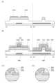
図1(A)は上面図であり、図1(A)に示す一点鎖線A1-A2方向の断面が図1(B
)に相当する。また、図1(A)に示す一点鎖線A3-A4方向の断面が図1(C)に相
当する。なお、図1(A)、(B)、(C)では、図の明瞭化のために一部の要素を拡大
、縮小、または省略して図示している。また、一点鎖線A1-A2方向をチャネル長方向
、一点鎖線A3-A4方向をチャネル幅方向と呼称する場合がある。FIG. 1A is a top view, and FIG. 1B is a cross section taken along the dashed line A1-A2 shown in FIG.
) corresponds to the cross section along the dashed line A3-A4 shown in FIG. 1A corresponds to FIG. 1C. In FIG. 1A, (B), and (C), some elements are enlarged, reduced, or omitted for clarity. The dashed line A1-A2 direction may be referred to as the channel length direction, and the dashed line A3-A4 direction may be referred to as the channel width direction.
なお、チャネル長とは、例えば、トランジスタの上面図において、半導体(またはトラン
ジスタがオン状態のときに半導体の中で電流の流れる部分)とゲート電極とが重なる領域
、またはチャネルが形成される領域における、ソース(ソース領域またはソース電極)と
ドレイン(ドレイン領域またはドレイン電極)との間の距離をいう。なお、一つのトラン
ジスタにおいて、チャネル長が全ての領域で同じ値をとるとは限らない。即ち、一つのト
ランジスタのチャネル長は、一つの値に定まらない場合がある。そのため、本明細書では
、チャネル長は、チャネルの形成される領域における、いずれか一の値、最大値、最小値
または平均値とする。Note that the channel length refers to, for example, the distance between the source (source region or source electrode) and the drain (drain region or drain electrode) in a region where the semiconductor (or the portion in the semiconductor through which current flows when the transistor is on) and the gate electrode overlap in a top view of the transistor, or in a region where a channel is formed. Note that the channel length of one transistor does not necessarily have the same value in all regions. That is, the channel length of one transistor may not be fixed to one value. Therefore, in this specification, the channel length is defined as any one value, maximum value, minimum value, or average value in the region where the channel is formed.
チャネル幅とは、例えば、半導体(またはトランジスタがオン状態のときに半導体の中で
電流の流れる部分)とゲート電極とが重なる領域、またはチャネルが形成される領域にお
ける、ソースとドレインとが向かい合っている部分の長さをいう。なお、一つのトランジ
スタにおいて、チャネル幅がすべての領域で同じ値をとるとは限らない。即ち、一つのト
ランジスタのチャネル幅は、一つの値に定まらない場合がある。そのため、本明細書では
、チャネル幅は、チャネルの形成される領域における、いずれか一の値、最大値、最小値
または平均値とする。The channel width refers to, for example, the length of the region where the semiconductor (or the portion in the semiconductor through which current flows when the transistor is on) and the gate electrode overlap, or the length of the portion where the source and drain face each other in the region where the channel is formed. Note that the channel width of one transistor does not necessarily have the same value in all regions. That is, the channel width of one transistor may not be determined to one value. Therefore, in this specification, the channel width is defined as any one value, maximum value, minimum value, or average value in the region where the channel is formed.
なお、トランジスタの構造によっては、実際にチャネルの形成される領域におけるチャネ
ル幅(以下、実効的なチャネル幅と呼ぶ。)と、トランジスタの上面図において示される
チャネル幅(以下、見かけ上のチャネル幅と呼ぶ。)と、が異なる場合がある。例えば、
立体的な構造を有するトランジスタでは、実効的なチャネル幅が、トランジスタの上面図
において示される見かけ上のチャネル幅よりも大きくなり、その影響が無視できなくなる
場合がある。例えば、微細かつ立体的な構造を有するトランジスタでは、半導体の上面に
形成されるチャネル領域の割合に対して、半導体の側面に形成されるチャネル領域の割合
が大きくなる場合がある。その場合は、上面図において示される見かけ上のチャネル幅よ
りも、実際にチャネルの形成される実効的なチャネル幅の方が大きくなる。Depending on the structure of a transistor, the channel width in a region where a channel is actually formed (hereinafter referred to as an effective channel width) may differ from the channel width shown in a top view of the transistor (hereinafter referred to as an apparent channel width).
In a transistor having a three-dimensional structure, the effective channel width may be larger than the apparent channel width shown in a top view of the transistor, and the influence of this may not be negligible. For example, in a transistor having a fine and three-dimensional structure, the proportion of the channel region formed on the side of the semiconductor may be larger than the proportion of the channel region formed on the top surface of the semiconductor. In this case, the effective channel width where the channel is actually formed is larger than the apparent channel width shown in the top view.
ところで、立体的な構造を有するトランジスタにおいては、実効的なチャネル幅の、実測
による見積もりが困難となる場合がある。例えば、設計値から実効的なチャネル幅を見積
もるためには、半導体の形状が既知という仮定が必要である。したがって、半導体の形状
が正確にわからない場合には、実効的なチャネル幅を正確に測定することは困難である。However, in a transistor having a three-dimensional structure, it may be difficult to estimate the effective channel width by actual measurement. For example, in order to estimate the effective channel width from a design value, it is necessary to assume that the shape of the semiconductor is known. Therefore, if the shape of the semiconductor is not known accurately, it is difficult to accurately measure the effective channel width.
そこで、本明細書では、トランジスタの上面図において、半導体とゲート電極とが重なる
領域における、ソースとドレインとが向かい合っている部分の長さである見かけ上のチャ
ネル幅を、「囲い込みチャネル幅(SCW:Surrounded Channel W
idth)」と呼ぶ場合がある。また、本明細書では、単にチャネル幅と記載した場合に
は、囲い込みチャネル幅または見かけ上のチャネル幅を指す場合がある。または、本明細
書では、単にチャネル幅と記載した場合には、実効的なチャネル幅を指す場合がある。な
お、チャネル長、チャネル幅、実効的なチャネル幅、見かけ上のチャネル幅、囲い込みチ
ャネル幅などは、断面TEM像などを取得して、その画像を解析することなどによって、
値を決定することができる。Therefore, in this specification, the apparent channel width, which is the length of the portion where the source and drain face each other in the region where the semiconductor and the gate electrode overlap in a top view of a transistor, is referred to as the "surrounded channel width (SCW)".
In this specification, when simply referred to as a channel width, it may refer to a surrounded channel width or an apparent channel width. In addition, in this specification, when simply referred to as a channel width, it may refer to an effective channel width. Note that the channel length, channel width, effective channel width, apparent channel width, surrounded channel width, etc. can be determined by obtaining a cross-sectional TEM image or the like and analyzing the image, etc.
A value can be determined.
なお、トランジスタの電界効果移動度や、チャネル幅当たりの電流値などを計算して求め
る場合、囲い込みチャネル幅を用いて計算する場合がある。その場合には、実効的なチャ
ネル幅を用いて計算する場合とは異なる値をとる場合がある。In addition, when calculating the field effect mobility of a transistor, the current value per channel width, and the like, the calculation may be performed using the enclosed channel width. In that case, the calculated value may be different from the value calculated using the effective channel width.
トランジスタ101は、基板110上の絶縁体120と、当該絶縁体120上の酸化物半
導体130と、当該酸化物半導体130と電気的に接続するソース電極140およびドレ
イン電極150と、酸化物半導体130、ソース電極140およびドレイン電極150上
のゲート絶縁体160と、酸化物半導体130、ソース電極140の一部およびドレイン
電極150の一部とゲート絶縁体160を介して重なるゲート電極170と、を有する。
また、ゲート絶縁体160およびゲート電極170上には絶縁体180を有していてもよ
い。また、絶縁体180上に酸化物で形成された絶縁体185が形成されていてもよい。
ただし、絶縁体185は有さなくてもよい。さらにその上部に他の絶縁体を形成してもよ
い。The
Also, an
However, the
本発明の一態様のトランジスタは、チャネル長が10nm以上300nm以下のトップゲ
ート型構造である。また、ゲート電極170とソース電極140とが互いに重なる領域1
91(LovS)およびゲート電極170とドレイン電極150とが互いに重なる領域1
92(LovD)を有する。領域191および領域192のチャネル長方向の幅は、寄生
容量を小さくするために3nm以上300nm未満とすることが好ましい。The transistor of one embodiment of the present invention has a top-gate structure and a channel length of 10 nm to 300 nm.
91 (LovS) and the
92 (LovD). The width of the
また、チャネルを形成する領域において、酸化物半導体130の膜厚は30nm以上30
0nm以下とすることが好ましい。例えば、100nm以上200nm以下とすることも
できる。なお、当該数値に絶縁体120のオーバーエッチングにて形成された凸部の高さ
が含まれていてもよい。即ち、当該凸部の高さと、酸化物半導体130の膜厚と、を併せ
て30nm以上300nm以下(例えば、100nm以上200nm以下)としても構わ
ない。In addition, in the region where a channel is formed, the thickness of the
It is preferable that the thickness of the
また、酸化物半導体130の膜厚をチャネル幅で除した値は、0.5以上とすることが好
ましい。例えば、0.5以上5以下または1以上3以下であることが好ましい。The value obtained by dividing the thickness of the
また、ゲート絶縁体160の厚さは、酸化膜換算膜厚で2nm以上30nm以下とするこ
とが好ましい。また、絶縁体120の厚さは、酸化膜換算膜厚で10nm以上1000n
m以下とすることが好ましい。The thickness of the
It is preferable that the length is set to m or less.
図1に示すトランジスタ101では、ゲート電極170は、酸化物半導体130のチャネ
ル幅方向を電気的に取り囲んだ構造となっている。特に、図2のように、ゲート電極17
0が酸化物半導体130を上面だけでなく側面も取り囲んでおり、かつ酸化物半導体13
0の下方まで伸びている構造となっていてもよい。このように、ゲート電極によって酸化
物半導体のチャネル幅方向を電気的に取り囲んだトランジスタの構造を、surroun
ded channel(s-channel)構造とよぶ。In the
0 surrounds the
0. The structure of a transistor in which the gate electrode electrically surrounds the oxide semiconductor in the channel width direction is called a surround structure.
This is called a dead channel (s-channel) structure.
トランジスタ101をsurrounded channel構造とし、チャネル幅を狭
くすることで、酸化物半導体130の側面に対してゲート電界によるキャリアの制御がし
やすくなる。そのため、良好なサブスレッショルド特性と極めて小さいオフ電流を有する
トランジスタ101が得られる。また、このような構造とすることで、酸化物半導体13
0の全体(バルク)にチャネルが形成される場合がある。s-channel構造では、
トランジスタのソース-ドレイン間に大電流を流すことができ、導通時の電流(オン電流
)を高くすることができる。By forming the
In some cases, a channel may be formed in the bulk of 0. In the s-channel structure,
A large current can be passed between the source and drain of the transistor, and the current when conductive (on-current) can be increased.
また、ソース電極140(および/または、ドレイン電極150)の、少なくとも一部(
または全部)は、酸化物半導体130などの半導体の、表面、側面、上面、および/また
は、下面の少なくとも一部(または全部)と、接触している。当該接触している酸化物半
導体130では、酸素欠損のサイトに水素が入り込むことでドナー準位を形成することが
あり、N型導電領域を有する。なお、酸素欠損のサイトに水素が入り込んだ状態をVOH
と表記する場合がある。その結果、N型導電領域を電流が流れることで、良好なオン電流
を得ることができる。In addition, at least a portion (
The
As a result, a current flows through the N-type conductive region, and a good on-current can be obtained.
また、酸化物半導体130のチャネル形成領域中の不純物濃度を低減し、酸化物半導体を
真性または実質的に真性にすることが有効である。ここで、実質的に真性とは、酸化物半
導体のキャリア密度が、1×10¹⁷個/cm3以下、好ましくは1×1015個/cm
3以下、さらに好ましくは1×10¹³個/cm3以下、より好ましくは1×1011個
/cm3以下、特に好ましくは1×1010個/cm3以下であり、1×10-9個/c
m3以上であることを指す。酸化物半導体において、水素、窒素、炭素、シリコン、およ
び主成分以外の金属元素は不純物となる。例えば、水素および窒素はドナー準位の形成に
寄与し、キャリア密度を増大させてしまう。It is also effective to reduce the impurity concentration in the channel formation region of the
3 or less, more preferably 1×10¹³ particles/cm3 or less, even more preferably 1×10¹¹ particles/cm3 or less, particularly preferably 1×10¹⁰ particles/cm3 or less, and 1×10⁻⁹ particles/cm
Inan oxide semiconductor, hydrogen, nitrogen, carbon, silicon, and metal elements other than the main components serve as impurities. For example, hydrogen and nitrogen contribute to the formation of a donor level and increase the carrier density.
当該酸化物半導体を用いたトランジスタは、チャネル形成領域におけるキャリア密度が低
いため、しきい値電圧がマイナスとなる電気特性になることが少ない。また、当該酸化物
半導体を用いたトランジスタは、酸化物半導体のキャリアトラップが少ないため、電気特
性の変動が小さく、信頼性の高いトランジスタとなる。また、当該酸化物半導体を用いた
トランジスタは、オフ電流を非常に低くすることが可能となる。Since the carrier density in a channel formation region of a transistor using the oxide semiconductor is low, the threshold voltage is unlikely to be a negative value. Since the transistor using the oxide semiconductor has few carrier traps in the oxide semiconductor, the change in the electrical characteristics is small, making the transistor highly reliable. Furthermore, the off-state current of the transistor using the oxide semiconductor can be made very low.
また、トランジスタ101が電子を多数キャリアとする蓄積型である場合、酸化物半導体
130のソース電極140およびドレイン電極150と接する領域からチャネル形成領域
へ延びる電界が遮蔽されやすく、短チャネルでもゲート電界によるキャリアの制御を行い
やすい。Furthermore, when the
また、絶縁表面上にトランジスタを形成することで、半導体基板をそのままチャネル形成
領域として用いる場合と異なり、ゲート電極と酸化物半導体もしくは半導体基板との間で
寄生容量が形成されないため、ゲート電界によるキャリアの制御が容易になる。また、良
好なスイッチング特性が得られる。In addition, by forming a transistor on an insulating surface, unlike the case where a semiconductor substrate is used as a channel formation region, no parasitic capacitance is formed between a gate electrode and an oxide semiconductor or a semiconductor substrate, which makes it easier to control carriers by a gate electric field, and good switching characteristics can be obtained.
このような構造とすることで、良好な電気特性が得られる。具体的には、優れたサブスレ
ッショルド特性、極めて小さいオフ電流、良好なオン電流が得られる。Such a structure provides good electrical characteristics, specifically, excellent subthreshold characteristics, extremely small off-current, and good on-current.
このような構造とすることで、微細なトランジスタにおいても良好な電気特性が得られる
。トランジスタの微細化により、トランジスタに寄生する各種容量が減少するため、良好
なスイッチング特性が得られる。With such a structure, good electrical characteristics can be obtained even in miniaturized transistors. Since various parasitic capacitances of the transistors are reduced by miniaturization of the transistors, good switching characteristics can be obtained.
一例として、チャネル長およびチャネル幅を50nmとすることができる。チャネルを形
成する領域において、酸化物半導体130の厚さを40nmとし、ゲート絶縁体160の
厚さを酸化膜換算膜厚で11nmとし、絶縁体120の厚さを酸化膜換算膜厚で390n
mとすることができる。For example, the channel length and the channel width can be set to 50 nm. In the region where the channel is formed, the thickness of the
m.
その結果、ゲート電圧3V、ドレイン電圧1V、ソース電圧0Vにおけるチャネル幅で規
格化したオン電流は58μA/μmで、かつ、オフ電流は0.1pA以下とすることがで
きる。また、しきい値電圧をプラスとすることができ(ノーマリオフの電気特性ともいう
)、さらには、ドレイン電流が1pAとなるゲート電圧が0V以上とすることも可能であ
る。また、DIBL(Drain Induced Barrier Lowering
)は、45mV/V以上100mV/V以下、代表的には67mV/V、SS(Subt
hreshold swing value)は60mV/dec以上120mV/de
c以下、代表的には92mV/decという優れた電気特性を得ることができる。As a result, the on-current normalized by the channel width at a gate voltage of 3 V, a drain voltage of 1 V, and a source voltage of 0 V is 58 μA/μm, and the off-current is 0.1 pA or less. In addition, the threshold voltage can be made positive (also called normally-off electrical characteristics), and further, the gate voltage at which the drain current becomes 1 pA can be made 0 V or more. In addition, DIBL (Drain Induced Barrier Lowering) is also possible.
) is 45mV/V or more and 100mV/V or less, typically 67mV/V, SS (Subt
threshold swing value) is 60mV/dec or more, 120mV/dec
c or less, typically 92 mV/dec, excellent electrical characteristics can be obtained.
このような構造のトランジスタを用いることにより、ノーマリオフであって、かつ、トラ
ンジスタのスイッチ速度が100ns未満、好ましくは10ns未満、10ps以上とす
ることができる。By using a transistor having such a structure, it is possible to make the transistor normally off and to make the switching speed of the transistor less than 100 ns, preferably less than 10 ns and 10 ps or more.
一例として、チャネル長64nm、チャネル幅68nmのトランジスタを書き込みトラン
ジスタとして用い、容量を充電させる場合、容量値14fFを持つ容量を約60nsで9
0%充電することができる。As an example, when a transistor having a channel length of 64 nm and a channel width of 68 nm is used as a write transistor and a capacitance is charged, a capacitance having a capacitance value of 14 fF is charged in about 60 ns.
It can be charged to 0%.
また、トランジスタのスイッチ速度が10ns未満、10ps以上、好ましくは3ns未
満、100ps以上とすることができる。Furthermore, the switching speed of the transistor can be set to less than 10 ns and 10 ps or more, and preferably less than 3 ns and 100 ps or more.
なお、トランジスタのスイッチ速度(スイッチングスピードとも呼ぶ)が速いとは、トラ
ンジスタのスイッチングに要する時間が短いことをいう。例えば、トランジスタのスイッ
チ速度とは、一つのトランジスタのゲート容量が90%充電されるのに要する時間を表し
、一つのトランジスタが負荷のない状態で非導通状態から導通状態となる時間を表す。こ
れは、ゲート電圧が変化した際に、トランジスタのドレイン電流の増分が、ゲート容量に
蓄積される電荷の増分を充電する時間と解釈することができる。または、トランジスタの
スイッチングに要する時間とは、トランジスタを増幅器として用いる場合に、電流利得が
1以上となる最大の周波数fT(遮断周波数ともいう)を用いて、1/(2×fT)で表
わす場合がある。または、電力利得が1以上となる最大の周波数fmax(最大発振周波
数ともいう)を用いて1/(2×fmax)で表わす場合がある。電力利得としては、単
方向電力利得や最大有能電力利得を用いることができる。In addition, the switching speed of a transistor is fast means that the time required for switching the transistor is short. For example, the switching speed of a transistor indicates the time required for the gate capacitance of one transistor to be charged by 90%, and indicates the time required for one transistor to go from a non-conducting state to a conducting state without a load. This can be interpreted as the time required for the increment of the drain current of the transistor to charge the increment of the charge stored in the gate capacitance when the gate voltage changes. Alternatively, the time required for switching the transistor may be expressed as 1/(2×fT ) using the maximum frequency fT (also called cutoff frequency) at which the current gain is 1 or more when the transistor is used as an amplifier. Alternatively, the time required for switching the transistor may be expressed as 1/(2×fmax ) using the maximum frequency fmax (also called maximum oscillation frequency) at which the power gain is 1 or more. As the power gain, a unidirectional power gain or a maximum available power gain may be used.
なお、スイッチ速度は、実際に測定してもよいし、計算によって検証してもよい。計算に
よって検証する場合には、SPICEを用いることができる。トランジスタモデルパラメ
ータは実際に測定したトランジスタの電気特性から抽出することが好ましい。電気特性の
測定は室温で行ってもよいし、低温(例えばー40℃)、高温(例えば125℃)におけ
る電気特性を合わせて測定してもよい。トランジスタモデルの一例として、RPI(Re
nsselaer Polytechnic Institute)モデルを用いること
ができる。また、レイアウトに基づいて、寄生容量や寄生抵抗といった寄生素子を抽出す
ることが好ましい。The switching speed may be actually measured or verified by calculation. When verifying by calculation, SPICE can be used. It is preferable to extract the transistor model parameters from the actually measured electrical characteristics of the transistor. The electrical characteristics may be measured at room temperature, or may be measured at low temperature (e.g., -40°C) and high temperature (e.g., 125°C). An example of a transistor model is RPI (Re
It is possible to use a model from the Institute of Electrical and Electronics Engineers (ISSEI). It is also preferable to extract parasitic elements such as parasitic capacitance and parasitic resistance based on the layout.
一例として、チャネル長64nm、チャネル幅68nmのトランジスタから抽出したトラ
ンジスタモデルパラメータを用いたSPICE計算において、1fF以下の容量を充電さ
せる場合、5ns以下で90%充電することができる。As an example, in a SPICE calculation using transistor model parameters extracted from a transistor having a channel length of 64 nm and a channel width of 68 nm, when a capacitance of 1 fF or less is charged, it can be charged to 90% in 5 ns or less.
また、このような構造のトランジスタを用いることにより、酸化膜換算膜厚で11nmと
いう比較的厚いゲート絶縁体でチャネル長が50nm程度まで短くなっても極小オフ電流
と、非常に良好なサブスレッショルド特性が得られる。Furthermore, by using a transistor having such a structure, even if the channel length is shortened to about 50 nm with a relatively thick gate insulator having an equivalent oxide thickness of 11 nm, a very small off-current and very good subthreshold characteristics can be obtained.
また、このような構造のトランジスタを用いることにより、酸化膜換算膜厚で11nmと
いう比較的厚いゲート絶縁体で、かつゲートオーバーラップ構造にもかかわらず、チャネ
ル長が50nm程度まで短くなっても極小オフ電流と、非常に良好なサブスレッショルド
特性が得られる。Furthermore, by using a transistor with such a structure, a very small off-state current and very good subthreshold characteristics can be obtained even when the channel length is shortened to about 50 nm, despite the relatively thick gate insulator with an equivalent oxide thickness of 11 nm and the gate overlap structure.
比較的厚いゲート絶縁体を用いることで、ゲート絶縁体を介したリーク電流が低減される
。また、薄いゲート絶縁体を形成する場合と比較して、容易に製造でき、膜厚ばらつきの
小さいゲート絶縁体を形成することが可能となる。The use of a relatively thick gate insulator reduces leakage current through the gate insulator and allows for the formation of a gate insulator that is easier to manufacture and has less variation in thickness than would be possible with a thinner gate insulator.
なお、トランジスタの「ソース」や「ドレイン」の機能は、異なる極性のトランジスタを
採用する場合や、回路動作において電流の方向が変化する場合などには入れ替わることが
ある。このため、本明細書においては、「ソース」や「ドレイン」という用語は、入れ替
えて用いることができるものとする。Note that the functions of the "source" and "drain" of a transistor may be interchanged when transistors of different polarity are used, when the direction of current flow changes during circuit operation, etc. For this reason, in this specification, the terms "source" and "drain" may be used interchangeably.
なお、ソース電極140(および/または、ドレイン電極150)の、少なくとも一部(
または全部)は、酸化物半導体130などの半導体の、表面、側面、上面、および/また
は、下面の少なくとも一部(または全部)に設けられている。In addition, at least a part (
The
または、ソース電極140(および/または、ドレイン電極150)の、少なくとも一部
(または全部)は、酸化物半導体130などの半導体の、表面、側面、上面、および/ま
たは、下面の少なくとも一部(または全部)と、接触している。または、ソース電極14
0(および/または、ドレイン電極150)の、少なくとも一部(または全部)は、酸化
物半導体130などの半導体の少なくとも一部(または全部)と、接触している。Alternatively, at least a part (or all) of the source electrode 140 (and/or the drain electrode 150) is in contact with at least a part (or all) of the surface, side, top, and/or bottom surface of the semiconductor such as the
At least a portion (or all) of the oxide semiconductor 130 (and/or the drain electrode 150 ) is in contact with at least a portion (or all) of a semiconductor such as the
または、ソース電極140(および/または、ドレイン電極150)の、少なくとも一部
(または全部)は、酸化物半導体130などの半導体の、表面、側面、上面、および/ま
たは、下面の少なくとも一部(または全部)と、電気的に接続されている。または、ソー
ス電極140(および/または、ドレイン電極150)の、少なくとも一部(または全部
)は、酸化物半導体130などの半導体の少なくとも一部(または全部)と、電気的に接
続されている。Alternatively, at least a part (or all) of the source electrode 140 (and/or the drain electrode 150) is electrically connected to at least a part (or all) of the surface, side, upper surface, and/or lower surface of a semiconductor such as the
または、ソース電極140(および/または、ドレイン電極150)の、少なくとも一部
(または全部)は、酸化物半導体130などの半導体の、表面、側面、上面、および/ま
たは、下面の少なくとも一部(または全部)に、近接して配置されている。または、ソー
ス電極140(および/または、ドレイン電極150)の、少なくとも一部(または全部
)は、酸化物半導体130などの半導体の少なくとも一部(または全部)に、近接して配
置されている。Alternatively, at least a part (or all) of the source electrode 140 (and/or the drain electrode 150) is disposed in proximity to at least a part (or all) of the surface, side, upper surface, and/or lower surface of a semiconductor such as the
または、ソース電極140(および/または、ドレイン電極150)の、少なくとも一部
(または全部)は、酸化物半導体130などの半導体の、表面、側面、上面、および/ま
たは、下面の少なくとも一部(または全部)の横側に配置されている。または、ソース電
極140(および/または、ドレイン電極150)の、少なくとも一部(または全部)は
、酸化物半導体130などの半導体の少なくとも一部(または全部)の横側に配置されて
いる。Alternatively, at least a portion (or all) of the source electrode 140 (and/or the drain electrode 150) is disposed on the lateral side of at least a portion (or all) of the surface, side, upper surface, and/or lower surface of a semiconductor such as the
または、ソース電極140(および/または、ドレイン電極150)の、少なくとも一部
(または全部)は、酸化物半導体130などの半導体の、表面、側面、上面、および/ま
たは、下面の少なくとも一部(または全部)の斜め上側に配置されている。または、ソー
ス電極140(および/または、ドレイン電極150)の、少なくとも一部(または全部
)は、酸化物半導体130などの半導体の少なくとも一部(または全部)の斜め上側に配
置されている。Alternatively, at least a part (or all) of the source electrode 140 (and/or the drain electrode 150) is disposed obliquely above at least a part (or all) of the front surface, side surface, upper surface, and/or lower surface of a semiconductor such as the
または、ソース電極140(および/または、ドレイン電極150)の、少なくとも一部
(または全部)は、酸化物半導体130などの半導体の、表面、側面、上面、および/ま
たは、下面の少なくとも一部(または全部)の上側に配置されている。または、ソース電
極140(および/または、ドレイン電極150)の、少なくとも一部(または全部)は
、酸化物半導体130などの半導体の少なくとも一部(または全部)の上側に配置されて
いる。Alternatively, at least a part (or all) of the source electrode 140 (and/or the drain electrode 150) is disposed on at least a part (or all) of the front surface, side surface, upper surface, and/or lower surface of a semiconductor such as the
また、トランジスタ101は、図3に示すように、酸化物半導体130と基板110との
間に導電体172を備えていてもよい。当該導電体を第2のゲート電極(バックゲート)
として用いることで、更なるオン電流の増加や、しきい値電圧の制御を行うことができる
。オン電流を増加させるには、例えば、ゲート電極170と導電体172を同電位として
トランジスタ101を駆動させればよい。また、しきい値電圧の制御を行うには、ゲート
電極170とは異なる定電位を導電体172に供給すればよい。3, the
By using the
また、本発明の一態様のトランジスタは、図4(A)、図4(B)および図4(C)に示
す構成であってもよい。図4(A)は上面図であり、図4(A)に示す一点鎖線B1-B
2方向の断面が図4(B)に相当する。また、図4(A)に示す一点鎖線B3-B4方向
の断面が図4(C)に相当する。なお、図4(A)、図4(B)および図4(C)では、
図の明瞭化のために一部の要素を拡大、縮小、または省略して図示している。また、一点
鎖線B1-B2方向をチャネル長方向、一点鎖線B3-B4方向をチャネル幅方向と呼称
する場合がある。The transistor of one embodiment of the present invention may have a structure illustrated in FIG. 4A, FIG. 4B, or FIG. 4C. FIG. 4A is a top view, and the dotted line B1-B in FIG.
The cross sections in the two directions correspond to Fig. 4(B). Also, the cross section in the direction of the dashed line B3-B4 shown in Fig. 4(A) corresponds to Fig. 4(C). Note that in Fig. 4(A), Fig. 4(B) and Fig. 4(C),
In order to clarify the drawings, some elements are enlarged, reduced, or omitted. Also, the direction of the dashed dotted line B1-B2 may be referred to as the channel length direction, and the direction of the dashed dotted line B3-B4 may be referred to as the channel width direction.
図4(A)、図4(B)および図4(C)に示すトランジスタ102は、酸化物半導体1
30が絶縁体120側から第1の酸化物半導体131、第2の酸化物半導体132、およ
び第3の酸化物半導体133の順で形成された点がトランジスタ101とは異なる。The
The
例えば、第1の酸化物半導体131、第2の酸化物半導体132、および第3の酸化物半
導体133には、それぞれ組成の異なる酸化物半導体などを用いることができる。ただし
、例えば、第1の酸化物半導体131と、第3の酸化物半導体133と、が同じまたはそ
の近傍の組成であってもよい。For example, oxide semiconductors having different compositions can be used as the
なお、トランジスタ101における酸化物半導体130の形状に関する説明は、トランジ
スタ102にも適用でき、同様の効果を得ることができる。また、図3に示す構成をトラ
ンジスタ102に適用することもできる。Note that the description regarding the shape of the
また、本発明の一態様のトランジスタは、図5(A)、図5(B)および図5(C)に示
す構成であってもよい。図5(A)は上面図であり、図5(A)に示す一点鎖線C1-C
2方向の断面が図5(B)に相当する。また、図5(A)に示す一点鎖線C3-C4方向
の断面が図5(C)に相当する。なお、図5(A)、図5(B)および図5(C)では、
図の明瞭化のために一部の要素を拡大、縮小、または省略して図示している。また、一点
鎖線C1-C2方向をチャネル長方向、一点鎖線C3-C4方向をチャネル幅方向と呼称
する場合がある。The transistor of one embodiment of the present invention may have a structure illustrated in FIG. 5A, FIG. 5B, or FIG. 5C. FIG. 5A is a top view, and the dashed line C1-C in FIG.
The cross sections in the two directions correspond to Fig. 5(B). Also, the cross section in the direction of the dashed line C3-C4 shown in Fig. 5(A) corresponds to Fig. 5(C). Note that in Figs. 5(A), 5(B) and 5(C),
In order to clarify the drawings, some elements are enlarged, reduced, or omitted. Also, the direction of the dashed dotted line C1-C2 may be referred to as the channel length direction, and the direction of the dashed dotted line C3-C4 may be referred to as the channel width direction.
図5(A)、図5(B)および図5(C)に示すトランジスタ103は、酸化物半導体1
30が絶縁体120側から第1の酸化物半導体131、第2の酸化物半導体132の順で
形成された積層と、当該積層の一部を覆う第3の酸化物半導体133を有する点が、トラ
ンジスタ101およびトランジスタ102とは異なる。The
The
例えば、第1の酸化物半導体131、第2の酸化物半導体132、および第3の酸化物半
導体133には、それぞれ組成の異なる酸化物半導体などを用いることができる。ただし
、例えば、第1の酸化物半導体131と、第3の酸化物半導体133と、が同じまたはそ
の近傍の組成であってもよい。For example, oxide semiconductors having different compositions can be used as the
具体的にトランジスタ103は、基板110上の絶縁体120と、当該絶縁体120上の
第1の酸化物半導体131、第2の酸化物半導体132の順で形成された積層と、当該積
層の一部と電気的に接続するソース電極140およびドレイン電極150と、当該積層の
一部、ソース電極140の一部、およびドレイン電極150の一部を覆う第3の酸化物半
導体133と、当該積層の一部、ソース電極140の一部、ドレイン電極150の一部、
第3の酸化物半導体133と重なるゲート絶縁体160およびゲート電極170と、を有
する。また、ソース電極140およびドレイン電極150、ならびにゲート電極170上
には絶縁体180が設けられていてもよい。また、絶縁体180上に酸化物で形成された
絶縁体185が形成されていてもよい。絶縁体185を有さなくてもよい。また、さらに
その上部に他の絶縁体を形成してもよい。Specifically, the
The semiconductor device has a
図1に示すトランジスタ101ではチャネルが形成される領域において酸化物半導体13
0は一層である。一方、図4に示すトランジスタ102では酸化物半導体130は基板1
10側から第1の酸化物半導体131、第2の酸化物半導体132、第3の酸化物半導体
133が積層された三層構造を有している。また、図5に示すトランジスタ103では、
トランジスタ102と同様に三層構造の酸化物半導体130を有している。一方、チャネ
ル形成領域において第2の酸化物半導体132は第1の酸化物半導体131および第3の
酸化物半導体133で取り囲まれている構造となっている。In the
On the other hand, in the
The
The
なお、トランジスタ102およびトランジスタ103の構造において、酸化物半導体13
0を構成する三層の材料を適切に選択することで電流を第2の酸化物半導体132の全体
に流すことができる。酸化物半導体130内部の第2の酸化物半導体132に電流が流れ
ることで、界面散乱の影響を受けにくく、高いオン電流を得ることができる。なお、第2
の酸化物半導体132を厚くすると、オン電流を向上させることができる。Note that in the structures of the
By appropriately selecting the materials of the three layers constituting the
When the
次に本発明の一態様のトランジスタの構成要素について詳細を説明する。Next, we will explain in detail the components of a transistor according to one embodiment of the present invention.
基板110は、単なる支持材料に限らず、他のトランジスタなどのデバイスが形成された
基板であってもよい。この場合、トランジスタのゲート電極170、ソース電極140、
およびドレイン電極150の一つは、上記の他のデバイスと電気的に接続されていてもよ
い。The
And one of the
絶縁体120は、基板110からの不純物の拡散を防止する役割を有するほか、酸化物半
導体130に酸素を供給する役割を担うことができる。したがって、絶縁体120は酸素
を含む絶縁体であることが好ましく、化学量論組成よりも多い酸素を含む絶縁体であるこ
とがより好ましい。例えば、昇温脱離ガス分光法(TDS:Thermal Desor
ption Spectrometry)にて、酸素原子に換算しての酸素の放出量が1
.0×1019atoms/cm3以上である膜とする。なお、上記TDS分析時におけ
る膜の表面温度としては100℃以上700℃以下、または100℃以上500℃以下の
範囲が好ましい。また、上述のように基板110が他のデバイスが形成された基板である
場合、絶縁体120は、層間絶縁体としての機能も有する。その場合は、表面が平坦にな
るようにCMP(Chemical Mechanical Polishing)法等
で平坦化処理を行うことが好ましい。The
In the optin spectrometry, the amount of oxygen released in terms of oxygen atoms was 1
The film has a surface concentration of 0.0×10¹⁹ atoms/cm3 or more. The surface temperature of the film during the TDS analysis is preferably in the range of 100° C. to 700° C., or 100° C. to 500° C. As described above, when the
なお、本実施の形態では、酸化物半導体130が三層構造である場合を主として詳細を説
明するが、積層数は問わない。トランジスタ101のように酸化物半導体130が一層の
場合は、本実施の形態で説明する第2の酸化物半導体132に相当する層を用いればよい
。また、酸化物半導体130が二層の場合は、例えば、トランジスタ102またはトラン
ジスタ103に示す酸化物半導体130の構成において、第3の酸化物半導体133を設
けない構成とすればよい。この構成の場合、第2の酸化物半導体132と第1の酸化物半
導体131を入れ替えることもできる。また、酸化物半導体130が四層以上である場合
は、例えば、本実施の形態で説明する三層構造の積層に対して他の酸化物半導体を積む構
成や当該三層構造におけるいずれかの界面に他の酸化物半導体を挿入する構成とすること
ができる。Note that in this embodiment, the
一例としては、第2の酸化物半導体132には、第1の酸化物半導体131および第3の
酸化物半導体133よりも電子親和力(真空準位から伝導帯下端までのエネルギー)が大
きい酸化物半導体を用いる。電子親和力は、真空準位と価電子帯上端とのエネルギー差(
イオン化ポテンシャル)から、伝導帯下端と価電子帯上端とのエネルギー差(エネルギー
ギャップ)を差し引いた値として求めることができる。For example, the
It can be calculated as the energy difference (energy gap) between the bottom of the conduction band and the top of the valence band from the ionization potential (EP).
第1の酸化物半導体131および第3の酸化物半導体133は、第2の酸化物半導体13
2を構成する金属元素を一種以上含み、例えば、伝導帯下端のエネルギーが第2の酸化物
半導体132よりも、0.05eV、0.07eV、0.1eV、0.15eVのいずれ
か以上であって、2eV、1eV、0.5eV、0.4eVのいずれか以下の範囲で真空
準位に近い酸化物半導体で形成することが好ましい。The
The
このような構造において、ゲート電極170に電界を印加すると、酸化物半導体130の
うち、伝導帯下端のエネルギーが最も小さい第2の酸化物半導体132にチャネルが形成
される。In such a structure, when an electric field is applied to the
また、第1の酸化物半導体131は、第2の酸化物半導体132を構成する金属元素を一
種以上含んで構成されるため、第2の酸化物半導体132と絶縁体120とが接した場合
の界面と比較して、第2の酸化物半導体132と第1の酸化物半導体131との界面には
界面準位を形成されにくくなる。該界面準位はチャネルを形成することがあるため、トラ
ンジスタのしきい値電圧が変動することがある。したがって、第1の酸化物半導体131
を設けることにより、トランジスタのしきい値電圧などの電気特性のばらつきを低減する
ことができる。また、当該トランジスタの信頼性を向上させることができる。Furthermore, since the
By providing the insulating film, variation in electrical characteristics such as a threshold voltage of a transistor can be reduced, and the reliability of the transistor can be improved.
また、第3の酸化物半導体133は、第2の酸化物半導体132を構成する金属元素を一
種以上含んで構成されるため、第2の酸化物半導体132とゲート絶縁体160が接した
場合の界面と比較して、第2の酸化物半導体132と第3の酸化物半導体133との界面
ではキャリアの散乱が起こりにくくなる。したがって、第3の酸化物半導体133を設け
ることにより、トランジスタの電界効果移動度を高くすることができる。Furthermore, since the
第1の酸化物半導体131および第3の酸化物半導体133には、例えば、Al、Ti、
Ga、Ge、Y、Zr、Sn、La、CeまたはHfを第2の酸化物半導体132よりも
高い原子数比で含む材料を用いることができる。具体的には、当該原子数比を1.5倍以
上、好ましくは2倍以上、さらに好ましくは3倍以上とする。前述の元素は酸素と強く結
合するため、酸素欠損が酸化物半導体に生じることを抑制する機能を有する。すなわち、
第1の酸化物半導体131および第3の酸化物半導体133は、第2の酸化物半導体13
2よりも酸素欠損が生じにくいと言うことができる。The
A material containing Ga, Ge, Y, Zr, Sn, La, Ce, or Hf at an atomic ratio higher than that of the
The
It can be said that oxygen deficiency is less likely to occur in this case than in the case of 2.
なお、第1の酸化物半導体131、第2の酸化物半導体132、第3の酸化物半導体13
3が、少なくともインジウム、亜鉛およびM(Al、Ti、Ga、Ge、Y、Zr、Sn
、La、CeまたはHf等の金属)を含むIn-M-Zn酸化物であるとき、第1の酸化
物半導体131をIn:M:Zn=x1:y1:z1[原子数比]、第2の酸化物半導体
132をIn:M:Zn=x2:y2:z2[原子数比]、第3の酸化物半導体133を
In:M:Zn=x3:y3:z3[原子数比]とすると、y1/x1およびy3/x3
がy2/x2よりも大きくなることが好ましい。y1/x1およびy3/x3はy2/x
2よりも1.5倍以上、好ましくは2倍以上、さらに好ましくは3倍以上とする。このと
き、第2の酸化物半導体132において、y2がx2以上であるとトランジスタの電気特
性を安定させることができる。ただし、y2がx2の3倍以上になると、トランジスタの
電界効果移動度が低下してしまうため、y2はx2の3倍未満であることが好ましい。Note that the
3 is at least indium, zinc and M (Al, Ti, Ga, Ge, Y, Zr, Sn
In the case of an In-M-Zn oxide containing an element (metal such as La, Ce, or Hf), when the
It is preferable thaty1 /x1 andy3 /x3 are greaterthany2 /x2 .
In the
第1の酸化物半導体131および第3の酸化物半導体133のZnおよびOを除いてのI
nおよびMの原子数比率は、好ましくはInが50atomic%未満、Mが50ato
mic%より高く、さらに好ましくはInが25atomic%未満、Mが75atom
ic%より高くする。また、第2の酸化物半導体132のZnおよびOを除いてのInお
よびMの原子数比率は、好ましくはInが25atomic%より高く、Mが75ato
mic%未満、さらに好ましくはInが34atomic%より高く、Mが66atom
ic%未満とする。I except for Zn and O in the
The atomic ratio of n and M is preferably less than 50 atomic % for In and less than 50 atomic % for M.
%, more preferably In is less than 25 atomic % and M is 75 atomic %.
The atomic ratio of In and M excluding Zn and O in the
%, more preferably In is higher than 34 atomic % and M is 66 atomic %.
It shall be less than IC%.
第1の酸化物半導体131および第3の酸化物半導体133の厚さは、3nm以上100
nm以下、好ましくは3nm以上50nm以下とする。また、第2の酸化物半導体132
の厚さは、3nm以上200nm以下、好ましくは10nm以上100nm以下、さらに
好ましくは10nm以上80nm以下とする。また、第2の酸化物半導体132は、第1
の酸化物半導体131および第3の酸化物半導体133より厚い方が好ましい。The
The thickness of the
The thickness of the
The thickness of the
なお、酸化物半導体をチャネルとするトランジスタに安定した電気特性を付与するために
は、酸化物半導体中の不純物濃度を低減し、酸化物半導体を真性または実質的に真性にす
ることが有効である。ここで、実質的に真性とは、酸化物半導体のキャリア密度が、1×
1017個/cm3以下、好ましくは1×1015個/cm3以下、さらに好ましくは1
×1013個/cm3以下、より好ましくは1×1011個/cm3以下、特に好ましく
は1×10¹⁰個/cm3以下であり、1×10-9個/cm3以上であることを指す。In order to provide a transistor having an oxide semiconductor as a channel with stable electrical characteristics, it is effective to reduce the impurity concentration in the oxide semiconductor so that the oxide semiconductor is intrinsic or substantially intrinsic.
1017 /cm3 or less, preferably 1 × 10¹⁵ /cm3 or less, more preferably 1
x 1013 particles/cm3 or less, more preferably 1 x 10¹¹ particles/cm3 or less, and particularly preferably 1 x 10¹⁰ particles/cm3 or less, and 1 x 10⁻⁹ particles/cm3 or more.
また、酸化物半導体において、水素、窒素、炭素、シリコン、および主成分以外の金属元
素は不純物となる。例えば、水素および窒素はドナー準位の形成に寄与し、キャリア密度
を増大させてしまう。また、シリコンは酸化物半導体中で不純物準位の形成に寄与する。
当該不純物準位はトラップとなり、トランジスタの電気特性を劣化させることがある。し
たがって、第1の酸化物半導体131、第2の酸化物半導体132および第3の酸化物半
導体133の層中や、それぞれの界面において不純物濃度を低減させることが好ましい。In an oxide semiconductor, hydrogen, nitrogen, carbon, silicon, and metal elements other than the main components act as impurities. For example, hydrogen and nitrogen contribute to the formation of donor levels and increase the carrier density. Silicon contributes to the formation of impurity levels in an oxide semiconductor.
The impurity levels become traps and may degrade the electrical characteristics of the transistor. Therefore, it is preferable to reduce the impurity concentrations in the
酸化物半導体を真性または実質的に真性とするためには、SIMS(Secondary
Ion Mass Spectrometry)分析において、例えば、酸化物半導体
のある深さにおいて、または、酸化物半導体のある領域において、シリコン濃度を1×1
019atoms/cm3未満、好ましくは5×1018atoms/cm3未満、さら
に好ましくは1×10¹⁸atoms/cm3未満とする。また、水素濃度は、例えば、
酸化物半導体のある深さにおいて、または、酸化物半導体のある領域において、2×10
20atoms/cm3以下、好ましくは5×1019atoms/cm3以下、より好
ましくは1×10¹⁹atoms/cm3以下、さらに好ましくは5×1018atom
s/cm3以下とする。また、窒素濃度は、例えば、酸化物半導体のある深さにおいて、
または、酸化物半導体のある領域において、5×10¹⁹atoms/cm3未満、好ま
しくは5×10¹⁸atoms/cm3以下、より好ましくは1×1018atoms/
cm3以下、さらに好ましくは5×10¹⁷atoms/cm3以下とする。In order to make the oxide semiconductor intrinsic or substantially intrinsic, a secondary ion beam (SIMS)
In the ion mass spectrometry (Ion Mass Spectrometry) analysis, for example, the silicon concentration is 1×1
The hydrogen concentration is, for example, less than0.19 atoms/cm.sup.3 , preferably less than5.times.10.sup.18 atoms/cm.sup.3 , and more preferably less than1.times.10.sup.18 atoms/cm.sup.3 .
At a certain depth in the oxide semiconductor or in a certain region in the oxide semiconductor,
20 atoms/cm3 or less, preferably 5×10¹⁹ atoms/cm3 orless , more preferably 1×10¹⁹ atoms/cm3 or less, and even more preferably 5×10¹⁸ atoms/cm3 or less.
The nitrogen concentration at a certain depth inthe oxide semiconductor is, for example,
Alternatively, in a region where the oxide semiconductor is present, the concentration is less than 5×10¹⁹ atoms/cm3 , preferably 5×10¹⁸ atoms/cm3 or less, more preferably 1×10¹⁸ atoms/
The concentration is preferably 5×10¹⁷ atoms/cm3 or less, and more preferably 5×10 17 atoms/cm3 or less.
また、酸化物半導体が結晶を含む場合、シリコンや炭素が高濃度で含まれると、酸化物半
導体の結晶性を低下させることがある。酸化物半導体の結晶性を低下させないためには、
例えば、酸化物半導体のある深さにおいて、または、酸化物半導体のある領域において、
シリコン濃度を1×10¹⁹atoms/cm3未満、好ましくは5×1018atom
s/cm3未満、さらに好ましくは1×1018atoms/cm3未満とすればよい。
また、例えば、酸化物半導体のある深さにおいて、または、酸化物半導体のある領域にお
いて、炭素濃度を1×10¹⁹atoms/cm3未満、好ましくは5×1018ato
ms/cm3未満、さらに好ましくは1×1018atoms/cm3未満とすればよい
。In addition, when an oxide semiconductor contains crystals, the crystallinity of the oxide semiconductor may be reduced if the oxide semiconductor contains silicon or carbon at a high concentration.
For example, at a certain depth in the oxide semiconductor or in a certain region in the oxide semiconductor,
The silicon concentration is set to less than 1×10¹⁹ atoms/cm3 , preferably less than 5×10¹⁸ atoms/
The concentration should be less than 1×10¹⁸ atoms/cm3 , and more preferably less than 1×10 18 atoms/cm3 .
For example, at a certain depth in the oxide semiconductor or in a certain region in the oxide semiconductor, the carbon concentration is set to less than 1×10¹⁹ atoms/cm3 , preferably less than 5×10¹⁸ atoms/
It is preferable that the concentration is less than 1×10¹⁸ atoms/cm3 , and more preferably less than 1×10 18 atoms/cm3 .
また、上述のように高純度化された酸化物半導体をチャネル形成領域に用いたトランジス
タのオフ電流は極めて小さい。例えば、ソースとドレインとの間の電圧を0.1V、5V
、または、10V程度とした場合に、トランジスタのチャネル幅で規格化したオフ電流を
数yA/μmから数zA/μmにまで低減することが可能となる。In addition, the off-state current of a transistor in which a highly purified oxide semiconductor is used for a channel formation region as described above is extremely small.
, or about 10 V, the off-state current normalized by the channel width of the transistor can be reduced from several yA/μm to several zA/μm.
また、上述のように高純度化された酸化物半導体は、キャリア発生源が少ないため、キャ
リア密度を低くすることができる。したがって、当該酸化物半導体を用いたトランジスタ
は、しきい値電圧がマイナスとなる電気特性になることが少ない。また、当該酸化物半導
体は、キャリアトラップが少ない。そのため、当該酸化物半導体を用いたトランジスタは
、電気特性の変動が小さく、信頼性の高いトランジスタとなる。In addition, since the highly purified oxide semiconductor as described above has a small carrier generation source, the carrier density can be reduced. Therefore, a transistor including the oxide semiconductor is unlikely to have electrical characteristics in which the threshold voltage is negative. In addition, the oxide semiconductor has few carrier traps. Therefore, the transistor including the oxide semiconductor has little fluctuation in its electrical characteristics and is highly reliable.
なお、トランジスタのゲート絶縁体としては、シリコンを含む絶縁体が多く用いられるた
め、上記理由により酸化物半導体のチャネルとなる領域は、本発明の一態様のトランジス
タのようにゲート絶縁体と接しない構造が好ましいということができる。また、ゲート絶
縁体と酸化物半導体との界面にチャネルが形成される場合、該界面でキャリアの散乱が起
こり、トランジスタの電界効果移動度が低くなることがある。このような観点からも、酸
化物半導体のチャネルとなる領域はゲート絶縁体から離すことが好ましいといえる。Note that since an insulator containing silicon is often used as the gate insulator of a transistor, for the above reasons, it is preferable that a region serving as a channel of the oxide semiconductor is not in contact with the gate insulator as in the transistor of one embodiment of the present invention. When a channel is formed at the interface between the gate insulator and the oxide semiconductor, carrier scattering occurs at the interface, which may reduce the field-effect mobility of the transistor. From this viewpoint, it is also preferable that the region serving as a channel of the oxide semiconductor is separated from the gate insulator.
したがって、酸化物半導体130を第1の酸化物半導体131、第2の酸化物半導体13
2、第3の酸化物半導体133の積層構造とすることで、第2の酸化物半導体132にチ
ャネルを形成することができ、高い電界効果移動度および安定した電気特性を有したトラ
ンジスタを形成することができる。また、良好なスイッチング特性が得られる。Therefore, the
By using a stacked structure of the
第1の酸化物半導体131、第2の酸化物半導体132、第3の酸化物半導体133のバ
ンド構造においては、伝導帯下端のエネルギーが連続的に変化する。これは、第1の酸化
物半導体131、第2の酸化物半導体132、第3の酸化物半導体133の組成が近似す
ることにより、酸素が相互に拡散しやすい点からも理解される。したがって、第1の酸化
物半導体131、第2の酸化物半導体132、第3の酸化物半導体133は組成が異なる
層の積層体ではあるが、物性的に連続であるということもでき、本明細書の図面において
、当該積層体のそれぞれの界面は点線で表している。In the band structures of the
主成分を共通として積層された酸化物半導体130は、各層を単に積層するのではなく連
続接合(ここでは特に伝導帯下端のエネルギーが各層の間で連続的に変化するU字型の井
戸構造(U Shape Well))が形成されるように作製する。すなわち、各層の
界面にトラップ中心や再結合中心のような欠陥準位を形成するような不純物濃度が低くな
るように積層構造を形成する。仮に、積層された酸化物半導体の層間に不純物が高濃度で
存在していると、エネルギーバンドの連続性が失われ、界面でキャリアがトラップあるい
は再結合により消滅してしまう場合がある。The
例えば、第1の酸化物半導体131および第3の酸化物半導体133にはIn:Ga:Z
n=1:3:2、1:3:3、1:3:4、1:3:6、1:6:4または1:9:6(
原子数比)、第2の酸化物半導体132にはIn:Ga:Zn=1:1:1、5:5:6
、または3:1:2(原子数比)などのIn-Ga-Zn酸化物などを用いることができ
る。また、第1の酸化物半導体131にIn:Ga:Zn=1:6:4または1:9:6
(原子数比)、第3の酸化物半導体133にIn:Ga:Zn=1:3:2、1:3:3
、1:3:4(原子数比)のIn-Ga-Zn酸化物などを用いてもよい。このような、
第1の酸化物半導体131、第2の酸化物半導体132および第3の酸化物半導体133
の成膜に、上述した原子数比の酸化物ターゲットを用いたスパッタリング法を用いると好
ましい。スパッタリング法を用いた場合、基板加熱温度にもよるが、成膜された酸化物半
導体の組成に対する亜鉛の比率が、ターゲットの組成と比べて20%から60%程度低減
する場合がある。また、成膜された酸化物半導体の組成に対するガリウムの比率が、ター
ゲットの組成と比べて1%から20%程度低減する場合がある。For example, the
n = 1:3:2, 1:3:3, 1:3:4, 1:3:6, 1:6:4 or 1:9:6 (
The
In the
The
Alternatively, an In-Ga-Zn oxide having an atomic ratio of 1:3:4 may be used.
A
It is preferable to use a sputtering method using an oxide target having the above atomic ratio for the deposition of the oxide semiconductor. When the sputtering method is used, the ratio of zinc to the composition of the deposited oxide semiconductor may be reduced by about 20% to 60% compared to the composition of the target, depending on the substrate heating temperature. Also, the ratio of gallium to the composition of the deposited oxide semiconductor may be reduced by about 1% to 20% compared to the composition of the target.
酸化物半導体130における第2の酸化物半導体132はウェル(井戸)となり、酸化物
半導体130を用いたトランジスタにおいて、チャネルは第2の酸化物半導体132に形
成される。なお、酸化物半導体130は伝導帯下端のエネルギーが連続的に変化している
ため、U字型井戸とも呼ぶことができる。また、このような構成で形成されたチャネルを
埋め込みチャネルということもできる。The
また、第1の酸化物半導体131および第3の酸化物半導体133と、酸化シリコン膜な
どの絶縁体との界面近傍には、不純物や欠陥に起因したトラップ準位が形成され得る。第
1の酸化物半導体131および第3の酸化物半導体133があることにより、第2の酸化
物半導体132と当該トラップ準位とを遠ざけることができる。Furthermore, trap states due to impurities or defects may be formed near interfaces between the
ただし、第1の酸化物半導体131および第3の酸化物半導体133の伝導帯下端のエネ
ルギーと、第2の酸化物半導体132の伝導帯下端のエネルギーとの差が小さい場合、第
2の酸化物半導体132の電子が該エネルギー差を越えてトラップ準位に達することがあ
る。マイナスの電荷となる電子がトラップ準位に捕獲されることで、トランジスタのしき
い値電圧はプラス方向にシフトしてしまう。However, when the difference between the energy of the conduction band minimum of the
したがって、トランジスタのしきい値電圧の変動を低減するには、第1の酸化物半導体1
31および第3の酸化物半導体133の伝導帯下端のエネルギーと、第2の酸化物半導体
132の伝導帯下端のエネルギーとの間に一定以上の差を設けることが好ましい。それぞ
れの当該エネルギー差は、0.1eV以上が好ましく、0.15eV以上がより好ましい
。Therefore, in order to reduce the fluctuation in the threshold voltage of the transistor, the
It is preferable to provide a certain or greater difference between the energy of the conduction band minimum of the
第1の酸化物半導体131、第2の酸化物半導体132および第3の酸化物半導体133
には、結晶部が含まれることが好ましい。特にc軸に配向した結晶を用いることでトラン
ジスタに安定した電気特性を付与することができる。A
It is preferable that the crystal portion is included. In particular, by using crystals oriented in the c-axis direction, stable electrical characteristics can be imparted to the transistor.
ソース電極140およびドレイン電極150には、酸化物半導体から酸素を引き抜く性質
を有する導電体を用いると好ましい。例えば、Al、Cr、Cu、Ta、Ti、Mo、W
などを用いることができる。上記材料において、特に酸素と結合しやすいTiや、後のプ
ロセス温度を比較的高く設定できる、融点の高いWを用いることがより好ましい。The
Of the above materials, it is more preferable to use Ti, which is particularly likely to bond with oxygen, or W, which has a high melting point and allows the subsequent process temperature to be set relatively high.
酸化物半導体から酸素を引き抜く性質を有する導電体の作用により、酸化物半導体中の酸
素が脱離し、酸化物半導体中に酸素欠損が形成される。当該酸化物半導体中に僅かに含ま
れる水素と当該酸素欠損が結合することにより当該領域は顕著にn型化する。したがって
、n型化した当該領域はトランジスタのソースまたはドレインとして作用させることがで
きる。Oxygen in the oxide semiconductor is released by the action of a conductor that has a property of extracting oxygen from the oxide semiconductor, and oxygen vacancies are formed in the oxide semiconductor. Hydrogen contained in a small amount in the oxide semiconductor is combined with the oxygen vacancies to remarkably change the region into an n-type region. Therefore, the n-type region can function as the source or drain of a transistor.
ゲート絶縁体160には、酸化アルミニウム、酸化マグネシウム、酸化シリコン、酸化窒
化シリコン、窒化酸化シリコン、窒化シリコン、酸化ガリウム、酸化ゲルマニウム、酸化
イットリウム、酸化ジルコニウム、酸化ランタン、酸化ネオジム、酸化ハフニウムおよび
酸化タンタルを一種以上含む絶縁体を用いることができる。また、ゲート絶縁体160は
上記材料の積層であってもよい。なお、ゲート絶縁体160に、ランタン(La)、窒素
、ジルコニウム(Zr)などを、不純物として含んでいてもよい。The
また、ゲート絶縁体160の積層構造の一例について説明する。ゲート絶縁体160は、
例えば、酸素、窒素、シリコン、ハフニウムなどを有する。具体的には、酸化ハフニウム
、および酸化シリコンまたは酸化窒化シリコンを含むと好ましい。An example of a stacked structure of the
For example, it contains oxygen, nitrogen, silicon, hafnium, etc. Specifically, it is preferable to contain hafnium oxide, silicon oxide, or silicon oxynitride.
酸化ハフニウムは、酸化シリコンや酸化窒化シリコンと比べて比誘電率が高い。したがっ
て、酸化膜換算膜厚に対して物理的な膜厚を大きくできるため、酸化膜換算膜厚を10n
m以下または5nm以下とした場合でも、トンネル電流によるリーク電流を小さくするこ
とができる。即ち、オフ電流の小さいトランジスタを実現することができる。さらに、結
晶構造を有する酸化ハフニウムは、非晶質構造を有する酸化ハフニウムと比べて高い比誘
電率を備える。したがって、オフ電流の小さいトランジスタとするためには、結晶構造を
有する酸化ハフニウムを用いることが好ましい。結晶構造の例としては、単斜晶系や立方
晶系などが挙げられる。ただし、本発明の一態様は、これらに限定されない。Hafnium oxide has a higher dielectric constant than silicon oxide or silicon oxynitride. Therefore, the physical thickness can be made larger than the equivalent oxide thickness.
Even when the thickness is set to 100 nm or less or 5 nm or less, the leakage current due to the tunnel current can be reduced. That is, a transistor with a small off-current can be realized. Furthermore, hafnium oxide having a crystalline structure has a higher relative dielectric constant than hafnium oxide having an amorphous structure. Therefore, in order to obtain a transistor with a small off-current, it is preferable to use hafnium oxide having a crystalline structure. Examples of the crystalline structure include a monoclinic system and a cubic system. However, one embodiment of the present invention is not limited thereto.
ところで、結晶構造を有する酸化ハフニウムの被形成面は、欠陥に起因した界面準位を有
する場合がある。該界面準位はトラップセンターとして機能する場合がある。そのため、
酸化ハフニウムがトランジスタのチャネル形成領域に近接して配置されるとき、該界面準
位によってトランジスタの電気特性が劣化する場合がある。そこで、該界面準位の影響を
低減するために、トランジスタのチャネル形成領域と酸化ハフニウムとの間に、別の膜を
配置することによって互いに離間させることが好ましい場合がある。この膜は、緩衝機能
を有する。緩衝機能を有する膜は、ゲート絶縁体160に含まれる膜であってもよいし、
酸化物半導体に含まれる膜であってもよい。即ち、緩衝機能を有する膜としては、酸化シ
リコン、酸化窒化シリコン、酸化物半導体などを用いることができる。なお、緩衝機能を
有する膜には、たとえば、チャネル形成領域となる半導体よりもエネルギーギャップの大
きい半導体または絶縁体を用いる。または、緩衝機能を有する膜には、たとえば、チャネ
ル形成領域となる半導体よりも電子親和力の小さい半導体または絶縁体を用いる。または
、緩衝機能を有する膜には、たとえば、チャネル形成領域となる半導体よりもイオン化エ
ネルギーの大きい半導体または絶縁体を用いる。Incidentally, the surface on which hafnium oxide having a crystalline structure is formed may have interface states due to defects. The interface states may function as trap centers.
When hafnium oxide is disposed close to a channel formation region of a transistor, the electrical characteristics of the transistor may be degraded due to the interface states. Therefore, in order to reduce the influence of the interface states, it may be preferable to separate the channel formation region of the transistor from the hafnium oxide by disposing another film between them. This film has a buffer function. The film having the buffer function may be a film included in the
The buffer film may be a film included in an oxide semiconductor. That is, silicon oxide, silicon oxynitride, an oxide semiconductor, or the like can be used as the film having a buffer function. Note that the buffer film may be made of, for example, a semiconductor or insulator having a larger energy gap than the semiconductor that will be the channel formation region. Alternatively, the buffer film may be made of, for example, a semiconductor or insulator having a smaller electron affinity than the semiconductor that will be the channel formation region. Alternatively, the buffer film may be made of, for example, a semiconductor or insulator having a larger ionization energy than the semiconductor that will be the channel formation region.
一方、上述した結晶構造を有する酸化ハフニウムの被形成面における界面準位(トラップ
センター)に電荷をトラップさせることで、トランジスタのしきい値電圧を制御できる場
合がある。該電荷を安定して存在させるためには、たとえば、チャネル形成領域と酸化ハ
フニウムとの間に、酸化ハフニウムよりもエネルギーギャップの大きい絶縁体を配置すれ
ばよい。または、酸化ハフニウムよりも電子親和力の小さい半導体または絶縁体を配置す
ればよい。または、緩衝機能を有する膜には、酸化ハフニウムよりもイオン化エネルギー
の大きい半導体または絶縁体を配置すればよい。このような絶縁体を用いることで、界面
準位にトラップされた電荷の放出が起こりにくくなり、長期間に渡って電荷を保持するこ
とができる。On the other hand, the threshold voltage of the transistor may be controlled by trapping the charge in the interface state (trap center) on the surface on which the hafnium oxide having the above-mentioned crystal structure is formed. In order to make the charge exist stably, for example, an insulator having a larger energy gap than hafnium oxide may be arranged between the channel formation region and the hafnium oxide. Alternatively, a semiconductor or insulator having a smaller electron affinity than hafnium oxide may be arranged in the film having a buffer function. By using such an insulator, the charge trapped in the interface state is less likely to be released, and the charge can be held for a long period of time.
そのような絶縁体として、例えば、酸化シリコン、酸化窒化シリコンが挙げられる。ゲー
ト絶縁体160内の界面準位に電荷を捕獲させるためには、酸化物半導体130からゲー
ト電極170に向かって電子を移動させればよい。具体的な例としては、高い温度(例え
ば、125℃以上450℃以下、代表的には150℃以上300℃以下)の下で、ゲート
電極170の電位をソース電極140やドレイン電極150の電位より高い状態にて1秒
以上、代表的には1分以上維持すればよい。Examples of such insulators include silicon oxide and silicon oxynitride. In order to trap charges at the interface state in the
このようにゲート絶縁体160などの界面準位に所望の量の電子を捕獲させたトランジス
タは、しきい値電圧がプラス側にシフトする。ゲート電極170の電圧や、電圧を印加す
る時間を調整することによって、電子を捕獲させる量(しきい値電圧の変動量)を制御す
ることができる。なお、電荷を捕獲させることができれば、ゲート絶縁体160内でなく
ても構わない。同様の構造を有する積層膜を、他の絶縁体に用いても構わない。In this way, a transistor in which a desired amount of electrons are trapped in the interface state of the
ゲート電極170には、Al、Ti、Cr、Co、Ni、Cu、Y、Zr、Mo、Ru、
Ag、TaおよびWなどの導電体を用いることができる。また、当該ゲート電極は、上記
材料の積層であってもよい。また、当該ゲート電極には、窒素を含んだ導電体を用いても
よい。The
Conductors such as Ag, Ta, and W can be used. The gate electrode may also be a stack of the above materials. The gate electrode may also be a conductor containing nitrogen.
ゲート絶縁体160、およびゲート電極170上に形成する絶縁体180には、酸化アル
ミニウム膜を含むことが好ましい。酸化アルミニウム膜は、水素、水分などの不純物、お
よび酸素の両方に対して膜を透過させない遮断効果が高い。したがって、酸化アルミニウ
ム膜は、トランジスタの作製工程中および作製後において、トランジスタの電気特性の変
動要因となる水素、水分などの不純物の酸化物半導体130への混入防止、酸化物半導体
130を構成する主成分材料である酸素の酸化物半導体からの放出防止、絶縁体120か
らの酸素の不必要な放出防止の効果を有する保護膜として用いることに適している。また
、酸化アルミニウム膜に含まれる酸素を酸化物半導体中に拡散させることもできる。The
また、絶縁体180上には絶縁体185が形成されていることが好ましい。絶縁体185
には、酸化マグネシウム、酸化シリコン、酸化窒化シリコン、窒化酸化シリコン、窒化シ
リコン、酸化ガリウム、酸化ゲルマニウム、酸化イットリウム、酸化ジルコニウム、酸化
ランタン、酸化ネオジム、酸化ハフニウムおよび酸化タンタルを一種以上含む絶縁体を用
いることができる。また、絶縁体185は上記材料の積層であってもよい。In addition, it is preferable that an
The
ここで、絶縁体185は絶縁体120と同様に化学量論組成よりも多くの酸素を有するこ
とが好ましい。絶縁体185から放出される酸素はゲート絶縁体160を経由して酸化物
半導体130のチャネル形成領域に拡散させることができることから、チャネル形成領域
に形成された酸素欠損に酸素を補填することができる。したがって、安定したトランジス
タの電気特性を得ることができる。Here, the
また、半導体装置を高集積化するにはトランジスタの微細化が必須である。一方、トラン
ジスタの微細化によりトランジスタの電気特性が悪化することが知られている。Further, miniaturization of transistors is essential for high integration of semiconductor devices, but it is known that miniaturization of transistors leads to deterioration of their electrical characteristics.
そこで、図5に示す本発明の一態様のトランジスタでは、前述したように、チャネルが形
成される第2の酸化物半導体132を覆うように第3の酸化物半導体133が形成されて
おり、チャネル形成層とゲート絶縁体が接しない構成となっている。そのため、チャネル
形成層とゲート絶縁体との界面で生じるキャリアの散乱を抑えることができ、トランジス
タのオン電流を大きくすることができる。その結果、良好なスイッチング特性が得られる
。5 according to one embodiment of the present invention, the
本発明の一態様のトランジスタでは、前述したように酸化物半導体130のチャネル幅方
向を電気的に取り囲むようにゲート電極170が形成されているため、酸化物半導体13
0に対しては垂直方向からのゲート電界に加えて、側面方向からのゲート電界が印加され
る。すなわち、酸化物半導体130の全体的にゲート電界が印加させることとなり、電流
はチャネルとなる第2の酸化物半導体132全体に流れるようになり、さらにオン電流を
高められる。その結果、良好なスイッチング特性が得られる。In the transistor of one embodiment of the present invention, the
For
また、本発明の一態様のトランジスタは、第2の酸化物半導体132を第1の酸化物半導
体131上に形成することで界面準位を形成しにくくする効果や、第2の酸化物半導体1
32を三層構造の中間に位置する層とすることで上下からの不純物混入の影響を排除でき
る効果などを併せて有する。そのため、上述したトランジスタのオン電流の向上に加えて
、しきい値電圧の安定化や、SSを向上させることができる。したがって、ゲート電圧V
gが0V時の電流を下げることができ、消費電力を低減させることができる。また、容量
に保持した電荷(あるいは情報)を当該トランジスタによって制御する場合に長期間にわ
たって保持(あるいは記憶)することができる。また、トランジスタのしきい値電圧が安
定化することから、半導体装置の長期信頼性を向上させることができる。In addition, in the transistor of one embodiment of the present invention, the
By making 32 the layer located in the middle of the three-layer structure, it is possible to eliminate the influence of impurities from above and below. Therefore, in addition to improving the on-current of the transistor as described above, it is possible to stabilize the threshold voltage and improve SS. Therefore, when the gate voltage V
The current when g is 0 V can be reduced, and power consumption can be reduced. Furthermore, when the charge (or information) held in the capacitance is controlled by the transistor, the charge (or information) can be held (or stored) for a long period of time. Furthermore, since the threshold voltage of the transistor is stabilized, the long-term reliability of the semiconductor device can be improved.
なお、本実施の形態は、本明細書で示す他の実施の形態および実施例と適宜組み合わせる
ことができる。Note that this embodiment mode can be appropriately combined with other embodiment modes and examples described in this specification.
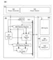
(実施の形態2)
本実施の形態では、本発明の一態様である図6に示すトランジスタ490の作製方法につ
いて説明する。図6(A)は、トランジスタ490の構成の一例を示す平面図である。図
6(B)には、図6(A)の一点鎖線E1-E2方向の断面図、および一点鎖線E3-E
4方向の断面図を示す。(Embodiment 2)
In this embodiment, a manufacturing method of a
Cross-sectional views in four directions are shown.
まず、絶縁体442を成膜する。絶縁体442は、スパッタリング法、化学気相成長(C
VD:Chemical Vapor Deposition)法、分子線エピタキシー
(MBE:Molecular Beam Epitaxy)法またはパルスレーザ堆積
(PLD:Pulsed Laser Deposition)法、原子層堆積(ALD
:Atomic Layer Deposition)法などを用いて成膜すればよい。First, the
Chemical Vapor Deposition (VD), Molecular Beam Epitaxy (MBE), Pulsed Laser Deposition (PLD), Atomic Layer Deposition (ALD)
The film may be formed by using a deposition technique such as atomic layer deposition (ALD).
絶縁体442は、金属または合金のターゲットを用い、DCスパッタリング法による成膜
すると好ましい。特に、反応性ガスとして酸素を用いたDCスパッタリング法では、ター
ゲット表面における反応が十分でないため、亜酸化物を含む絶縁体が成膜できる場合があ
る。亜酸化物は、水素や酸素などを捕獲して安定化する場合がある。したがって、絶縁体
442が亜酸化物を含む絶縁体である場合、水素や酸素などに対するブロック性の高い絶
縁体であることがわかる。The
なお、CVD法は、プラズマを利用するプラズマCVD(PECVD:Plasma E
nhanced CVD)法、熱を利用する熱CVD(TCVD:Thermal CV
D)法などに分類できる。さらに用いる原料ガスによって金属CVD(MCVD:Met
al CVD)法、有機金属CVD(MOCVD:Metal Organic CVD
)法に分けることができる。The CVD method is a plasma enhanced CVD (PECVD) method that uses plasma.
Improved CVD (CVD), Thermal CVD (TCVD)
Furthermore, depending on the source gas used, it can be classified into metal CVD (MCVD: Met
al CVD) method, Metal Organic CVD (MOCVD)
) laws.
プラズマCVD法は、比較的低温で高品質の膜が得られる。熱CVD法は、プラズマを用
いないため、プラズマダメージが生じず、欠陥の少ない膜が得られる。The plasma CVD method can obtain a high-quality film at a relatively low temperature, and the thermal CVD method does not use plasma, so no plasma damage occurs and a film with few defects can be obtained.
CVD法は、原料ガスの流量比によって、得られる膜の組成を制御することができる。例
えば、MCVD法およびMOCVD法では、原料ガスの流量比によって、任意の組成の膜
を成膜することができる。また、例えば、MCVD法およびMOCVD法では、成膜しな
がら原料ガスの流量比を変化させることによって、組成が連続的に変化した膜を成膜する
ことができる。原料ガスの流量比を変化させながら成膜する場合、複数の成膜室を用いて
成膜する場合と比べて、搬送や圧力調整に掛かる時間の分、成膜に掛かる時間を短くする
ことができる。したがって、トランジスタ490の生産性を高めることができる。In the CVD method, the composition of the film obtained can be controlled by the flow rate ratio of the source gas. For example, in the MCVD method and the MOCVD method, a film of any composition can be formed by changing the flow rate ratio of the source gas. In addition, for example, in the MCVD method and the MOCVD method, a film whose composition changes continuously can be formed by changing the flow rate ratio of the source gas while forming the film. When forming a film while changing the flow rate ratio of the source gas, the time required for film formation can be shortened by the time required for transportation and pressure adjustment compared to the case of forming a film using a plurality of film formation chambers. Therefore, the productivity of the
次に、導電体413となる導電体を成膜する。導電体413となる導電体は、スパッタリ
ング法、CVD法、MBE法またはPLD法、ALD法などを用いて成膜すればよい。Next, a conductor is formed to become the
次に、導電体413となる導電体の一部をエッチングし、導電体413を形成する。Next, a portion of the conductor that will become
次に、絶縁体402を成膜する(図7(A)参照。)。絶縁体402は、スパッタリング
法、CVD法、MBE法またはPLD法、ALD法などを用いて成膜すればよい。なお、
ここでは、絶縁体402は、CMP法などによって、上面から平坦化する場合について説
明する。絶縁体402の上面を平坦化することで、後の工程が容易となり、トランジスタ
490の歩留まりを高くすることができる。例えば、CMP法によって、絶縁体402の
RMS(Root Mean Square:二乗平均平方根)粗さを1nm以下、好ま
しくは0.5nm以下、さらに好ましくは0.3nm以下とする。または、1μm×1μ
mの範囲におけるRa(平均面粗さ)を1nm未満、好ましくは0.6nm未満、さらに
好ましくは0.5nm未満、より好ましくは0.4nm未満とする。または、1μm×1
μmの範囲におけるPeak-Valleyを10nm未満、好ましくは9nm未満、さ
らに好ましくは8nm未満、より好ましくは7nm未満とする。ただし、本発明の一態様
に係るトランジスタ490は、絶縁体402の上面を平坦化した場合に限定されない。Next, the
Here, the case where the
The Ra (average surface roughness) in the range of 1 μm×1 μm is set to less than 1 nm, preferably less than 0.6 nm, more preferably less than 0.5 nm, and even more preferably less than 0.4 nm.
The peak-valley in the μm range is set to less than 10 nm, preferably less than 9 nm, further preferably less than 8 nm, and further preferably less than 7 nm. However, the
絶縁体402は、過剰酸素を含ませるように成膜すればよい。または、絶縁体402の成
膜後に酸素を添加しても構わない。酸素の添加は、例えば、イオン注入法により、加速電
圧を2kV以上100kV以下とし、ドーズ量を5×10¹⁴ions/cm2以上5×
1016ions/cm2以下として行えばよい。The
It is sufficient to set the concentration at 1016 ions/cm2 or less.
なお、絶縁体402を積層膜で構成する場合には、それぞれの膜を、上記のような成膜方
法を用いて、異なる成膜方法で成膜してもよい。例えば、1層目をCVD法で成膜し、2
層目をALD法で成膜してもよい。または、1層目をスパッタリング法で成膜し、2層目
をALD法で成膜してもよい。このように、それぞれ異なる成膜方法を用いることによっ
て、各層の膜に異なる機能や性質を持たせることができる。そして、それらの膜を積層す
ることによって、積層膜全体として、より適切な膜を構成することができる。In addition, when the
The first layer may be formed by the ALD method. Alternatively, the first layer may be formed by the sputtering method and the second layer may be formed by the ALD method. In this way, by using different film formation methods, it is possible to give each layer different functions and properties. Then, by stacking these films, it is possible to form a more suitable film as a whole laminated film.
つまり、n層目(nは自然数)の膜を、スパッタリング法、CVD法、MBE法またはP
LD法、ALD法などのうちの少なくとも1つの方法で成膜し、n+1層目の膜を、スパ
ッタリング法、CVD法、MBE法またはPLD法、ALD法などのうちの少なくとも1
つの方法で成膜する。なお、n層目の膜と、n+1層目の膜とで、成膜方法が同じでも異
なっていてもよい。なお、n層目の膜とn+2層目の膜とで、成膜方法が同じでもよい。
または、すべての膜において、成膜方法が同じでもよい。That is, the nth layer (n is a natural number) is formed by sputtering, CVD, MBE or P
The n+1th layer is formed by at least one of the following methods: sputtering, CVD, MBE, PLD, ALD, etc.
The film is formed by one of the methods. The film formation methods for the nth layer and the (n+1)th layer may be the same or different. The film formation methods for the nth layer and the (n+2)th layer may be the same.
Alternatively, the deposition method may be the same for all the films.
次に、半導体406aとなる半導体436a、および半導体406bとなる半導体436
bをこの順に成膜する。半導体406aとなる半導体436a、および半導体406bと
なる半導体436bは、スパッタリング法、CVD法、MBE法またはPLD法、ALD
法などを用いて成膜すればよい。Next, a
The
The film may be formed by using a method such as a method for forming a thin film.
なお、半導体436aおよび半導体436bとして、In-Ga-Zn酸化物層をMOC
VD法によって成膜する場合、原料ガスとしてトリメチルインジウム、トリメチルガリウ
ムおよびジメチル亜鉛などを用いればよい。なお、上記原料ガスの組み合わせに限定され
ず、トリメチルインジウムに代えてトリエチルインジウムなどを用いてもよい。また、ト
リメチルガリウムに代えてトリエチルガリウムなどを用いてもよい。また、ジメチル亜鉛
に代えてジエチル亜鉛などを用いてもよい。The
When forming a film by the VD method, trimethylindium, trimethylgallium, dimethylzinc, or the like may be used as a source gas. The combination of source gases is not limited to the above, and triethylindium, or the like may be used instead of trimethylindium. Triethylgallium, or the like may be used instead of trimethylgallium. Diethylzinc, or the like may be used instead of dimethylzinc.
次に、第1の加熱処理を行うと好ましい。第1の加熱処理は、250℃以上650℃以下
、好ましくは300℃以上500℃以下で行えばよい。第1の加熱処理は、不活性ガス雰
囲気、または酸化性ガスを10ppm以上、1%以上もしくは10%以上含む雰囲気で行
う。第1の加熱処理は減圧状態で行ってもよい。または、第1の加熱処理は、不活性ガス
雰囲気で加熱処理した後に、脱離した酸素を補うために酸化性ガスを10ppm以上、1
%以上または10%以上含む雰囲気で加熱処理を行ってもよい。第1の加熱処理によって
、半導体436a、および半導体436bの結晶性を高めることや、水素や水などの不純
物を除去すること等ができる。Next, a first heat treatment is preferably performed. The first heat treatment may be performed at 250° C. to 650° C., preferably 300° C. to 500° C. The first heat treatment is performed in an inert gas atmosphere or an atmosphere containing 10 ppm or more, 1% or more, or 10% or more of an oxidizing gas. The first heat treatment may be performed under reduced pressure. Alternatively, the first heat treatment may be performed in an inert gas atmosphere, followed by adding 10 ppm or more, 1% or more of an oxidizing gas to compensate for the desorbed oxygen.
% or more or 10% or more of Cd may be used. By the first heat treatment, the crystallinity of the
次に、導電体416を成膜する(図7(B)参照。)。導電体416は、スパッタリング
法、CVD法、MBE法またはPLD法、ALD法などを用いて成膜すればよい。Next, a
導電体416aおよび導電体416bは、導電体416を成膜した後で、導電体416の
一部をエッチングすることで形成される。したがって、導電体416の成膜時に、半導体
406bへダメージを与えない成膜方法を用いると好ましい。即ち、導電体416の成膜
には、MCVD法などを用いると好ましい。The
なお、導電体416を積層膜で構成する場合には、それぞれの膜を、スパッタリング法、
CVD法(プラズマCVD法、熱CVD法、MCVD法、MOCVD法など)、MBE法
、PLD法、ALD法などのような成膜方法を用いて、異なる成膜方法で成膜してもよい
。例えば、1層目をMOCVD法で成膜し、2層目をスパッタリング法で成膜してもよい
。または、1層目をALD法で成膜し、2層目をMOCVD法で成膜してもよい。または
、1層目をALD法で成膜し、2層目をスパッタリング法で成膜してもよい。または、1
層目をALD法で成膜し、2層目をスパッタリング法で成膜し、3層目をALD法で成膜
してもよい。このように、それぞれ、異なる成膜方法を用いることによって、各層の膜に
異なる機能や性質を持たせることができる。そして、それらの膜を積層することによって
、積層膜全体として、より適切な膜を構成することができる。When the
The films may be formed by different film formation methods such as CVD (plasma CVD, thermal CVD, MCVD, MOCVD, etc.), MBE, PLD, ALD, etc. For example, the first layer may be formed by MOCVD, and the second layer may be formed by sputtering. Alternatively, the first layer may be formed by ALD, and the second layer may be formed by MOCVD. Alternatively, the first layer may be formed by ALD, and the second layer may be formed by sputtering. Alternatively, the first layer may be formed by ALD, and the second layer may be formed by sputtering.
The first layer may be formed by ALD, the second layer by sputtering, and the third layer by ALD. In this way, by using different film formation methods, each layer can have different functions and properties. By stacking these films, a more suitable film can be formed as a laminate film as a whole.
つまり、導電体416を積層膜で構成する場合には、例えば、n層目の膜を、スパッタリ
ング法、CVD法(プラズマCVD法、熱CVD法、MCVD法、MOCVD法など)、
MBE法、PLD法、ALD法などのうちの少なくとも1つの方法で成膜し、n+1層目
の膜を、スパッタリング法、CVD法(プラズマCVD法、熱CVD法、MCVD法、M
OCVD法など)、MBE法、PLD法、ALD法などのうちの少なくとも1つの方法で
成膜し、n層目の膜と、n+1層目の膜とで、成膜方法が異なっていてもよい(nは自然
数)。なお、n層目の膜とn+2層目の膜とで、成膜方法が同じでもよい。または、すべ
ての膜において、成膜方法が同じでもよい。That is, when the
The n+1 layer is formed by at least one of the methods of MBE, PLD, ALD, etc., and the n+1 layer is formed by sputtering, CVD (plasma CVD, thermal CVD, MCVD, M
The nth film and the n+1th film may be formed by at least one of the following methods: OCVD, MBE, PLD, ALD, etc. (n is a natural number). The nth film and the n+2th film may be formed by the same method. Alternatively, all the films may be formed by the same method.
なお、導電体416、または導電体416の積層膜の内の少なくとも一つの膜と、半導体
406aとなる半導体436a、または半導体406bとなる半導体436bとは、同じ
成膜方法を用いてもよい。例えば、どちらも、ALD法を用いてもよい。これにより、大
気に触れさせずに成膜することができる。その結果、不純物の混入を防ぐことができる。Note that the
なお、導電体416、または導電体416の積層膜の内の少なくとも一つの膜と、半導体
406aとなる半導体436a、または半導体406bとなる半導体436bと、絶縁体
402、または絶縁体402の積層膜の内の少なくとも一つの膜とは、同じ成膜方法を用
いてもよい。例えば、どれも、スパッタリング法を用いてもよい。これにより、大気に触
れさせずに成膜することができる。その結果、不純物の混入を防ぐことができる。ただし
、本発明の一態様に係る半導体装置の作製方法は、これらに限定されない。Note that the
次に、マスク426を形成する(図8(A)参照。)。マスク426は、感光性を有する
レジストを用いればよい。なお、マスク426として、フォトレジストの下地に、反射防
止膜(BARC:Bottom Anti Reflective Coating)を
設けてもよい。反射防止膜を設けることで、ハレーションによる不良を抑制することがで
き、微細な形状を得ることができる。Next, a
次に、マスク426をマスクに用いて、導電体416をエッチングし、導電体417を形
成する。なお、微細な形状を有する導電体417を形成するためには、微細な形状を有す
るマスク426を形成することになる。微細な形状を有するマスク426は、厚すぎると
倒れる場合があるため、自立できる程度の厚さの領域を有すると好ましい。また、マスク
426をマスクとしてエッチングする導電体416は、マスク426が耐えうる条件でエ
ッチングされる程度に薄いことが好ましい。ただし、導電体416は、後にトランジスタ
490のソース電極およびドレイン電極としての機能を有する導電体416aおよび導電
体416bとなるため、トランジスタ490のオン電流を大きくするためにはある程度の
厚さがあるほうが好ましい。したがって、例えば、5nm以上30nm以下、好ましくは
5nm以上20nm以下、さらに好ましくは5nm以上15nm以下の厚さの領域を有す
る導電体416とすればよい。Next, the
次に、導電体417をマスクに用いて、半導体436bおよび半導体436aをエッチン
グし、半導体406aおよび半導体406bを形成する。このとき、絶縁体402までエ
ッチングすると、s-channel構造が形成されやすくなる(図8(B)参照。)。Next, the
次に、導電体417の一部をエッチングし、導電体416aおよび導電体416bを形成
する(図9(A)参照。)。このように、半導体436aおよび半導体436bをエッチ
ングするためのマスクとして形成された導電体416は、トランジスタ490のソース電
極およびドレイン電極としての機能を有する導電体416aおよび導電体416bとなる
。導電体416aおよび導電体416bとなる導電体416をマスクとしても用いること
から、トランジスタ490を作製するための工程数を低減できる。また、トランジスタ4
90は、導電体416aおよび導電体416bの占有面積を小さくすることができるため
、微細な半導体装置に適した構造である。Next, part of the
The
次に、半導体406cとなる半導体を成膜する。半導体406cとなる半導体は、スパッ
タリング法、CVD法、MBE法またはPLD法、ALD法などを用いて成膜すればよい
。Next, a semiconductor to be the
なお、半導体406cとなる半導体として、In-Ga-Zn酸化物層をMOCVD法に
よって成膜する場合、原料ガスとしてトリメチルインジウム、トリメチルガリウムおよび
ジメチル亜鉛などを用いればよい。なお、上記原料ガスの組み合わせに限定されず、トリ
メチルインジウムに代えてトリエチルインジウムなどを用いてもよい。また、トリメチル
ガリウムに代えてトリエチルガリウムなどを用いてもよい。また、ジメチル亜鉛に代えて
ジエチル亜鉛などを用いてもよい。When an In-Ga-Zn oxide layer is formed by MOCVD as the
次に、第2の加熱処理を行っても構わない。例えば、半導体406aとして、半導体40
6cとなる半導体よりも酸素透過性の高い半導体を選択する。即ち、半導体406cとな
る半導体として、半導体406aよりも酸素透過性の低い半導体を選択する。換言すると
、半導体406aとして、酸素を透過する機能を有する半導体を選択する。また、半導体
406cとなる半導体として、酸素をブロックする機能を有する半導体を選択する。この
とき、第2の加熱処理を行うことで、半導体406aを介して、絶縁体402に含まれる
過剰酸素が半導体406bまで移動する。半導体406bは半導体406cとなる半導体
で覆われているため、過剰酸素の外方拡散が起こりにくい。そのため、このタイミングで
第2の加熱処理を行うことで、効率的に半導体406bの欠陥(酸素欠損)を低減するこ
とができる。なお、第2の加熱処理は、絶縁体402中の過剰酸素(酸素)が半導体40
6bまで拡散する温度で行えばよい。例えば、第1の加熱処理についての記載を参照して
も構わない。または、第2の加熱処理は、第1の加熱処理よりも低い温度が好ましい。低
下させる温度範囲は、20℃以上150℃以下、好ましくは40℃以上100℃以下とす
る。これにより、絶縁体402から余分に過剰酸素(酸素)が放出することを抑えること
ができる。。Next, a second heat treatment may be performed.
A semiconductor having higher oxygen permeability than the
The second heat treatment may be performed at a temperature at which the oxygen diffuses to the
次に、絶縁体412となる絶縁体を成膜する。絶縁体412となる絶縁体は、スパッタリ
ング法、CVD法、MBE法またはPLD法、ALD法などを用いて成膜すればよい。Next, an insulator to be the
なお、絶縁体412となる絶縁体を積層膜で構成する場合には、それぞれの膜を、スパッ
タリング法、CVD法(プラズマCVD法、熱CVD法、MCVD法、MOCVD法など
)、MBE法、PLD法、ALD法などのような成膜方法を用いて、異なる成膜方法で成
膜してもよい。例えば、1層目をMOCVD法で成膜し、2層目をスパッタリング法で成
膜してもよい。または、1層目をALD法で成膜し、2層目をMOCVD法で成膜しても
よい。または、1層目をALD法で成膜し、2層目をスパッタリング法で成膜してもよい
。または、1層目をALD法で成膜し、2層目をスパッタリング法で成膜し、3層目をA
LD法で成膜してもよい。このように、それぞれ、異なる成膜方法を用いることによって
、各層の膜に異なる機能や性質を持たせることができる。そして、それらの膜を積層する
ことによって、積層膜全体として、より適切な膜を構成することができる。In addition, when the insulator to be
The films may be formed by the LD method. In this way, by using different film formation methods, it is possible to give each layer a different function or property. By stacking these films, it is possible to form a more suitable film as a whole laminated film.
つまり、絶縁体412となる絶縁体を積層膜で構成する場合には、例えば、n層目の膜を
、スパッタリング法、CVD法(プラズマCVD法、熱CVD法、MCVD法、MOCV
D法など)、MBE法、PLD法、ALD法などのうちの少なくとも1つの方法で成膜し
、n+1層目の膜を、スパッタリング法、CVD法(プラズマCVD法、熱CVD法、M
CVD法、MOCVD法など)、MBE法、PLD法、ALD法などのうちの少なくとも
1つの方法で成膜し、n層目の膜と、n+1層目の膜とで、成膜方法が異なっていてもよ
い(nは自然数)。なお、n層目の膜とn+2層目の膜とで、成膜方法が同じでもよい。
または、すべての膜において、成膜方法が同じでもよい。That is, when the
The n+1 layer is formed by at least one method selected from the group consisting of a sputtering method, a CVD method (plasma CVD method, thermal CVD method, MBE method, PLD method, ALD method, etc.), and the n+2 layer is formed by at least one method selected from the group consisting of a sputtering method, a CVD method (plasma CVD method, thermal CVD method, M
The nth film and the n+1th film may be formed by at least one of the following methods: CVD, MOCVD, MBE, PLD, ALD, etc., and the film formation method may be different (n is a natural number). Note that the nth film and the n+2th film may be formed by the same film formation method.
Alternatively, the deposition method may be the same for all the films.
次に、第3の加熱処理を行っても構わない。例えば、半導体406aとして、半導体40
6cとなる半導体よりも酸素透過性の高い半導体を選択する。即ち、半導体406cとな
る半導体として、半導体406aよりも酸素透過性の低い半導体を選択する。また、半導
体406cとなる半導体として、酸素をブロックする機能を有する半導体を選択する。ま
たは、例えば、半導体406aとして、絶縁体412となる絶縁体よりも酸素透過性の高
い半導体を選択する。即ち、絶縁体412となる絶縁体として、半導体406aよりも酸
素透過性の低い絶縁体を選択する。換言すると、半導体406aとして、酸素を透過する
機能を有する半導体を選択する。また、絶縁体412となる絶縁体として、酸素をブロッ
クする機能を有する絶縁体を選択する。このとき、第3の加熱処理を行うことで、半導体
406aを介して、絶縁体402に含まれる過剰酸素が半導体406bまで移動する。半
導体406bは半導体406cとなる半導体および絶縁体412となる絶縁体で覆われて
いるため、過剰酸素の外方拡散が起こりにくい。そのため、このタイミングで第3の加熱
処理を行うことで、効率的に半導体406bの欠陥(酸素欠損)を低減することができる
。なお、第3の加熱処理は、絶縁体402中の過剰酸素(酸素)が半導体406bまで拡
散する温度で行えばよい。例えば、第1の加熱処理についての記載を参照しても構わない
。または、第3の加熱処理は、第1の加熱処理よりも低い温度が好ましい。低下させる温
度範囲は、20℃以上150℃以下、好ましくは40℃以上100℃以下とする。なお、
絶縁体412となる絶縁体が酸素をブロックする機能を有する場合、半導体406cとな
る半導体が酸素をブロックする機能を有さなくても構わない。Next, a third heat treatment may be performed.
A semiconductor having a higher oxygen permeability than the
In the case where the insulator to be the
次に、導電体404となる導電体を成膜する。導電体404となる導電体は、スパッタリ
ング法、CVD法、MBE法またはPLD法、ALD法などを用いて成膜すればよい。Next, a conductor is formed to become the
絶縁体412となる絶縁体は、トランジスタ490のゲート絶縁体として機能する。した
がって導電体404となる導電体の成膜時に、絶縁体412となる絶縁体へダメージを与
えない成膜方法を用いると好ましい。即ち、該導電体の成膜には、MCVD法などを用い
ると好ましい。The insulator that becomes the
なお、導電体404となる導電体を積層膜で構成する場合には、それぞれの膜を、スパッ
タリング法、CVD法(プラズマCVD法、熱CVD法、MCVD法、MOCVD法など
)、MBE法、PLD法、ALD法などのような成膜方法を用いて、異なる成膜方法で成
膜してもよい。例えば、1層目をMOCVD法で成膜し、2層目をスパッタリング法で成
膜してもよい。または、1層目をALD法で成膜し、2層目をMOCVD法で成膜しても
よい。または、1層目をALD法で成膜し、2層目をスパッタリング法で成膜してもよい
。または、1層目をALD法で成膜し、2層目をスパッタリング法で成膜し、3層目をA
LD法で成膜してもよい。このように、それぞれ、異なる成膜方法を用いることによって
、各層の膜に異なる機能や性質を持たせることができる。そして、それらの膜を積層する
ことによって、積層膜全体として、より適切な膜を構成することができる。In addition, when the conductor to be the
The films may be formed by the LD method. In this way, by using different film formation methods, it is possible to give each layer a different function or property. By stacking these films, it is possible to form a more suitable film as a whole laminated film.
つまり、導電体404となる導電体を積層膜で構成する場合には、例えば、n層目の膜を
、スパッタリング法、CVD法(プラズマCVD法、熱CVD法、MCVD法、MOCV
D法など)、MBE法、PLD法、ALD法などのうちの少なくとも1つの方法で成膜し
、n+1層目の膜を、スパッタリング法、CVD法(プラズマCVD法、熱CVD法、M
CVD法、MOCVD法など)、MBE法、PLD法、ALD法などのうちの少なくとも
1つの方法で成膜し、n層目の膜と、n+1層目の膜とで、成膜方法が異なっていてもよ
い(nは自然数)。なお、n層目の膜とn+2層目の膜とで、成膜方法が同じでもよい。
または、すべての膜において、成膜方法が同じでもよい。That is, when the conductor to be the
The n+1 layer is formed by at least one method selected from the group consisting of a sputtering method, a CVD method (plasma CVD method, thermal CVD method, MBE method, PLD method, ALD method, etc.), and the n+2 layer is formed by at least one method selected from the group consisting of a sputtering method, a CVD method (plasma CVD method, thermal CVD method, M
The nth film and the n+1th film may be formed by at least one of the following methods: CVD, MOCVD, MBE, PLD, ALD, etc., and the film formation method may be different (n is a natural number). Note that the nth film and the n+2th film may be formed by the same film formation method.
Alternatively, the deposition method may be the same for all the films.
なお、導電体404となる導電体、または導電体404となる導電体の積層膜の内の少な
くとも一つの膜と、絶縁体412となる絶縁体、または絶縁体412となる絶縁体の積層
膜の内の少なくとも一つの膜とは、同じ成膜方法を用いてもよい。例えば、どちらも、A
LD法を用いてもよい。これにより、大気に触れさせずに成膜することができる。その結
果、不純物の混入を防ぐことができる。または、例えば、絶縁体412となる絶縁体と接
する導電体404となる導電体と、導電体404となる導電体と接する絶縁体412とな
る絶縁体とは、同じ成膜方法を用いてもよい。これにより、同じチャンバーで成膜するこ
とができる。その結果、不純物の混入を防ぐことができる。The conductor to be the
An LD method may be used. This allows the film to be formed without exposure to the air. As a result, the inclusion of impurities can be prevented. Alternatively, for example, the same film formation method may be used for the conductor that becomes the
なお、導電体404となる導電体、または導電体404となる導電体の積層膜の内の少な
くとも一つの膜と、絶縁体412となる絶縁体、または絶縁体412となる絶縁体の積層
膜の内の少なくとも一つの膜とは同じ成膜方法を用いてもよい。例えば、どれも、スパッ
タリング法を用いてもよい。これにより、大気に触れさせずに成膜することができる。そ
の結果、不純物の混入を防ぐことができる。Note that the conductor that becomes the
次に、導電体404となる導電体の一部をエッチングして導電体404を形成する。なお
、導電体404は、半導体406bの少なくとも一部と重なるように形成する。Next, part of the conductor that is to become the
次に、導電体404となる導電体と同様に、絶縁体412となる絶縁体の一部をエッチン
グして絶縁体412を形成する。Next, similar to the conductor that becomes the
次に、導電体404となる導電体および絶縁体412となる絶縁体と同様に、半導体40
6cとなる半導体の一部をエッチングして半導体406cを形成する。Next, the
A part of the semiconductor that will become 6c is etched to form a
なお、導電体404となる導電体、絶縁体412となる絶縁体および半導体406cとな
る半導体の一部をエッチングする際には、同一のフォトリソグラフィ工程など用いてもよ
い。または、導電体404をマスクとして用いて絶縁体412となる絶縁体および半導体
406cとなる半導体をエッチングしてもよい。そのため、導電体404、絶縁体412
および半導体406cは、上面図において同様の形状となる。なお、図9(C1)に示す
拡大断面のように、導電体404よりも絶縁体412または/および半導体406cが突
出した(迫り出した)形状となる場合や、図9(C2)に示す拡大断面のように、導電体
404が絶縁体412または/および半導体406cよりも突出した(迫り出した)形状
となる場合がある。これらに示すような形状とすることによって、形状不良が低減され、
ゲートリーク電流を低減できる場合がある。Note that when etching the conductor to be the
9C1, the
The gate leakage current may be reduced.
次に、絶縁体408を成膜する(図9(B)参照。)。絶縁体408は、スパッタリング
法、CVD法、MBE法またはPLD法、ALD法などを用いて成膜すればよい。Next, the
次に、第4の加熱処理を行っても構わない。例えば、半導体406aとして、半導体40
6cよりも酸素透過性の高い半導体を選択する。即ち、半導体406cとして、半導体4
06aよりも酸素透過性の低い半導体を選択する。また、半導体406cとして、酸素を
ブロックする機能を有する半導体を選択する。または、例えば、半導体406aとして、
絶縁体412よりも酸素透過性の高い半導体を選択する。即ち、絶縁体412として、半
導体406aよりも酸素透過性の低い半導体を選択する。または、例えば、半導体406
aとして、絶縁体408よりも酸素透過性の高い半導体を選択する。即ち、絶縁体408
として、半導体406aよりも酸素透過性の低い半導体を選択する。換言すると、半導体
406aとして、酸素を透過する機能を有する半導体を選択する。また、絶縁体408と
して、酸素をブロックする機能を有する絶縁体を選択する。このとき、第4の加熱処理を
行うことで、半導体406aを介して、絶縁体402に含まれる過剰酸素が半導体406
bまで移動する。半導体406bは半導体406c、絶縁体412、絶縁体408のいず
れかで覆われているため、過剰酸素の外方拡散が起こりにくい。そのため、このタイミン
グで第4の加熱処理を行うことで、効率的に半導体406bの欠陥(酸素欠損)を低減す
ることができる。なお、第4の加熱処理は、絶縁体402中の過剰酸素(酸素)が半導体
406bまで拡散する温度で行えばよい。例えば、第1の加熱処理についての記載を参照
しても構わない。または、第4の加熱処理は、第1の加熱処理よりも低い温度が好ましい
。低下させる温度範囲は、20℃以上150℃以下、好ましくは40℃以上100℃以下
とする。なお、絶縁体408が酸素をブロックする機能を有する場合、半導体406cま
たは/および絶縁体412が酸素をブロックする機能を有さなくても構わない。Next, a fourth heat treatment may be performed.
A semiconductor having higher oxygen permeability than
For example, a semiconductor having a function of blocking oxygen is selected as the
A semiconductor having higher oxygen permeability than the
A semiconductor having a higher oxygen permeability than the
In other words, a semiconductor that transmits oxygen is selected as the
b. The
なお、第1の加熱処理、第2の加熱処理、第3の加熱処理および第4の加熱処理の全てま
たは一部を行わなくても構わない。Note that all or some of the first heat treatment, the second heat treatment, the third heat treatment, and the fourth heat treatment do not necessarily have to be performed.
次に、絶縁体418を成膜する。絶縁体418は、スパッタリング法、CVD法、MBE
法またはPLD法、ALD法などを用いて成膜すればよい。Next, the
The film may be formed by a deposition method, a PLD method, an ALD method, or the like.
以上のようにして、図6に示したトランジスタ490を作製することができる。In this manner, the
なお、本実施の形態は、本明細書で示す他の実施の形態および実施例と適宜組み合わせる
ことができる。Note that this embodiment mode can be appropriately combined with other embodiment modes and examples described in this specification.
(実施の形態3)
本実施の形態では、本発明の一態様であるトランジスタに使用することができる酸化物半
導体について説明する。(Embodiment 3)
In this embodiment, an oxide semiconductor that can be used for a transistor according to one embodiment of the present invention will be described.
酸化物半導体は、非単結晶酸化物半導体と単結晶酸化物半導体とに大別される。非単結晶
酸化物半導体とは、CAAC-OS(C Axis Aligned Crystall
ine Oxide Semiconductor)、多結晶酸化物半導体、微結晶酸化
物半導体、非晶質酸化物半導体などをいう。なお、CAAC-OSをCANC-OS(C
Axis Aligned Nano Crystalline Oxide Sem
iconductor)と呼ぶこともできる。Oxide semiconductors are roughly classified into non-single-crystal oxide semiconductors and single-crystal oxide semiconductors.
CAAC-OS refers to a semiconductor material such as a crystal oxide semiconductor, a polycrystalline oxide semiconductor, a microcrystalline oxide semiconductor, or an amorphous oxide semiconductor.
Axis Aligned Nano Crystalline Oxide Sem
It can also be called an I conductor.
まずは、CAAC-OSについて説明する。First, let me explain about CAAC-OS.
CAAC-OSは、c軸配向した複数の結晶部を有する酸化物半導体の一つである。CAAC-OS is a type of oxide semiconductor that has multiple crystal parts aligned along the c-axis.
透過型電子顕微鏡(TEM:Transmission Electron Micro
scope)によって、CAAC-OSの明視野像および回折パターンの複合解析像(高
分解能TEM像ともいう。)を観察することで複数の結晶部を確認することができる。一
方、高分解能TEM像によっても明確な結晶部同士の境界、即ち結晶粒界(グレインバウ
ンダリーともいう。)を確認することができない。そのため、CAAC-OSは、結晶粒
界に起因する電子移動度の低下が起こりにくいといえる。Transmission Electron Microscope (TEM)
By observing a composite analysis image (also referred to as a high-resolution TEM image) of a bright-field image and a diffraction pattern of the CAAC-OS using a TEM (transmission electron microscope) scope, multiple crystalline parts can be confirmed. On the other hand, even in a high-resolution TEM image, clear boundaries between crystalline parts, that is, crystal grain boundaries, cannot be confirmed. Therefore, it can be said that the decrease in electron mobility due to crystal grain boundaries is unlikely to occur in the CAAC-OS.
試料面と略平行な方向から、CAAC-OSの断面の高分解能TEM像を観察すると、結
晶部において、金属原子が層状に配列していることを確認できる。金属原子の各層は、C
AAC-OSを形成する面(被形成面ともいう。)または上面の凹凸を反映した形状であ
り、CAAC-OSの被形成面または上面と平行に配列する。When a high-resolution TEM image of a cross section of CAAC-OS is observed from a direction substantially parallel to the sample surface, it can be seen that metal atoms are arranged in layers in the crystal part.
The shape of the AAC-OS reflects the unevenness of a surface (also referred to as a surface on which the AAC-OS is formed) or a top surface, and the CAAC-OS is arranged in parallel to the surface on which the CAAC-OS is formed or the top surface.
本明細書において、「平行」とは、二つの直線が-10°以上10°以下の角度で配置さ
れている状態をいう。したがって、-5°以上5°以下の場合も含まれる。また、「略平
行」とは、二つの直線が-30°以上30°以下の角度で配置されている状態をいう。ま
た、「垂直」とは、二つの直線が80°以上100°以下の角度で配置されている状態を
いう。したがって、85°以上95°以下の場合も含まれる。また、「略垂直」とは、二
つの直線が60°以上120°以下の角度で配置されている状態をいう。In this specification, "parallel" refers to a state in which two straight lines are arranged at an angle of -10° or more and 10° or less. Therefore, the case of -5° or more and 5° or less is also included. Furthermore, "substantially parallel" refers to a state in which two straight lines are arranged at an angle of -30° or more and 30° or less. Furthermore, "perpendicular" refers to a state in which two straight lines are arranged at an angle of 80° or more and 100° or less. Therefore, the case of 85° or more and 95° or less is also included. Furthermore, "substantially perpendicular" refers to a state in which two straight lines are arranged at an angle of 60° or more and 120° or less.
一方、試料面と略垂直な方向から、CAAC-OSの平面の高分解能TEM像を観察する
と、結晶部において、金属原子が三角形状または六角形状に配列していることを確認でき
る。しかしながら、異なる結晶部間で、金属原子の配列に規則性は見られない。On the other hand, when a high-resolution TEM image of a plane of CAAC-OS is observed from a direction substantially perpendicular to the sample surface, it can be seen that metal atoms are arranged in a triangular or hexagonal shape in the crystal parts, but no regularity is observed in the arrangement of metal atoms between different crystal parts.
図38(A)は、CAAC-OSの断面の高分解能TEM像である。また、図38(B)
は、図38(A)をさらに拡大した断面の高分解能TEM像であり、理解を容易にするた
めに原子配列を強調表示している。FIG. 38A is a high-resolution TEM image of a cross section of CAAC-OS.
38(A) is a high-resolution TEM image of a cross section further enlarged from FIG. 38(A), in which the atomic arrangement is highlighted for ease of understanding.
図38(C)は、図38(A)のA-O-A’間において、丸で囲んだ領域(直径約4n
m)の局所的なフーリエ変換像である。図38(C)より、各領域においてc軸配向性が
確認できる。また、A-O間とO-A’間とでは、c軸の向きが異なるため、異なるグレ
インであることが示唆される。また、A-O間では、c軸の角度が14.3°、16.6
°、26.4°のように少しずつ連続的に変化していることがわかる。同様に、O-A’
間では、c軸の角度が-18.3°、-17.6°、-15.9°と少しずつ連続的に変
化していることがわかる。FIG. 38C shows the area surrounded by a circle (diameter: about 4n) between A-O-A' in FIG. 38A.
38(C) is a localized Fourier transform image of the lattice structure of the SiO2-Al2O3 grains. From FIG. 38(C), the c-axis orientation can be confirmed in each region. In addition, the c-axis orientation is different between A-O and O-A', suggesting that they are different grains. In addition, the c-axis angle is 14.3° and 16.6° between A-O.
26.4°, and so on.
It can be seen that the c-axis angle changes gradually and continuously between −18.3°, −17.6°, and −15.9°.
なお、CAAC-OSに対し、電子回折を行うと、配向性を示すスポット(輝点)が観測
される。例えば、CAAC-OSの上面に対し、例えば1nm以上30nm以下の電子線
を用いる電子回折(ナノビーム電子回折ともいう。)を行うと、スポットが観測される(
図39(A)参照。)。When electron diffraction is performed on the CAAC-OS, spots (bright points) showing orientation are observed. For example, when electron diffraction (also referred to as nanobeam electron diffraction) is performed on the top surface of the CAAC-OS using an electron beam with a diameter of 1 nm to 30 nm, spots are observed (
See Figure 39(A).
断面の高分解能TEM像および平面の高分解能TEM像より、CAAC-OSの結晶部は
配向性を有していることがわかる。The high-resolution cross-sectional TEM image and the high-resolution planar TEM image show that the crystal parts of the CAAC-OS have orientation.
なお、CAAC-OSに含まれるほとんどの結晶部は、一辺が100nm未満の立方体内
に収まる大きさである。したがって、CAAC-OSに含まれる結晶部は、一辺が10n
m未満、5nm未満または3nm未満の立方体内に収まる大きさの場合も含まれる。ただ
し、CAAC-OSに含まれる複数の結晶部が連結することで、一つの大きな結晶領域を
形成する場合がある。例えば、平面の高分解能TEM像において、2500nm2以上、
5μm2以上または1000μm2以上となる結晶領域が観察される場合がある。Most of the crystal parts included in the CAAC-OS are sized to fit within a cube with one side less than 100 nm.
However, a plurality of crystal parts included in the CAAC-OS may be connected to form a single large crystal region. For example, a high-resolution TEM image of a plane may have a size of 2500 nm ormore ,
Crystalline regions of5 μm2 or more or 1000 μm2 ormore may be observed.
CAAC-OSに対し、X線回折(XRD:X-Ray Diffraction)装置
を用いて構造解析を行うと、例えばInGaZnO4の結晶を有するCAAC-OSのo
ut-of-plane法による解析では、回折角(2θ)が31°近傍にピークが現れ
る場合がある。このピークは、InGaZnO4の結晶の(009)面に帰属されること
から、CAAC-OSの結晶がc軸配向性を有し、c軸が被形成面または上面に略垂直な
方向を向いていることが確認できる。When the structure of CAAC-OS is analyzed using an X-ray diffraction (XRD) device, for example, the o-phase structure of CAAC-OS having InGaZnO4 crystals is
In the analysis by the out-of-plane method, a peak may appear at a diffraction angle (2θ) of approximately 31°. This peak is attributed to the (009) plane of the InGaZnO4 crystal, and therefore it can be confirmed that the CAAC-OS crystal has a c-axis orientation, and the c-axis faces in a direction approximately perpendicular to the surface on which the CAAC-OS is formed or the upper surface.
一方、CAAC-OSに対し、c軸に略垂直な方向からX線を入射させるin-plan
e法による解析では、2θが56°近傍にピークが現れる場合がある。このピークは、I
nGaZnO4の結晶の(110)面に帰属される。InGaZnO4の単結晶酸化物半
導体であれば、2θを56°近傍に固定し、試料面の法線ベクトルを軸(φ軸)として試
料を回転させながら分析(φスキャン)を行うと、(110)面と等価な結晶面に帰属さ
れるピークが6本観察される。これに対し、CAAC-OSの場合は、2θを56°近傍
に固定してφスキャンした場合でも、明瞭なピークが現れない。On the other hand, in-plan X-ray irradiation is performed on CAAC-OS from a direction substantially perpendicular to the c-axis.
In the analysis by the Ie method, a peak may appear at 2θ of about 56°.
The peaks are attributed to the (110) plane of the crystal of InGaZnO4. In the case of a single crystal oxide semiconductor of InGaZnO4 , when 2θ is fixed at about 56° and an analysis (φ scan) is performed while rotating the sample around the axis (φ axis) of the normal vector of the sample surface, six peaks are observed that are attributed to a crystal plane equivalent to the (110) plane. In contrast, in the case of CAAC-OS, no clear peaks appear even when 2θ is fixed at about 56° and φ scan is performed.
以上のことから、CAAC-OSでは、異なる結晶部間ではa軸およびb軸の配向は不規
則であるが、c軸配向性を有し、かつc軸が被形成面または上面の法線ベクトルに平行な
方向を向いていることがわかる。したがって、前述の断面の高分解能TEM観察で確認さ
れた層状に配列した金属原子の各層は、結晶のab面に平行な面である。From the above, it can be seen that in CAAC-OS, the a-axis and b-axis orientations are irregular between different crystal parts, but the c-axis has a c-axis orientation, and the c-axis is parallel to the normal vector of the surface on which it is formed or the top surface. Therefore, each layer of metal atoms arranged in layers confirmed by the high-resolution TEM observation of the cross section described above is a plane parallel to the a-b plane of the crystal.
なお、結晶部は、CAAC-OSを成膜した際、または加熱処理などの結晶化処理を行っ
た際に形成される。上述したように、結晶のc軸は、CAAC-OSの被形成面または上
面の法線ベクトルに平行な方向に配向する。したがって、例えば、CAAC-OSの形状
をエッチングなどによって変化させた場合、結晶のc軸がCAAC-OSの被形成面また
は上面の法線ベクトルと平行にならないこともある。The crystal parts are formed when the CAAC-OS is formed or when a crystallization treatment such as heat treatment is performed. As described above, the c-axis of the crystal is oriented in a direction parallel to the normal vector of the surface on which the CAAC-OS is formed or the top surface. Therefore, for example, when the shape of the CAAC-OS is changed by etching or the like, the c-axis of the crystal may not be parallel to the normal vector of the surface on which the CAAC-OS is formed or the top surface.
また、CAAC-OS中において、c軸配向した結晶部の分布が均一でなくてもよい。例
えば、CAAC-OSの結晶部が、CAAC-OSの上面近傍からの結晶成長によって形
成される場合、上面近傍の領域は、被形成面近傍の領域よりもc軸配向した結晶部の割合
が高くなることがある。また、不純物の添加されたCAAC-OSは、不純物が添加され
た領域が変質し、部分的にc軸配向した結晶部の割合の異なる領域が形成されることもあ
る。Furthermore, the distribution of c-axis oriented crystal parts in the CAAC-OS does not have to be uniform. For example, when the crystal parts of the CAAC-OS are formed by crystal growth from the vicinity of the top surface of the CAAC-OS, the region near the top surface may have a higher proportion of c-axis oriented crystal parts than the region near the surface on which the CAAC-OS is formed. Furthermore, in the CAAC-OS to which an impurity is added, the region to which the impurity is added may be altered, and a region with a different proportion of c-axis oriented crystal parts may be formed.
なお、InGaZnO4の結晶を有するCAAC-OSのout-of-plane法に
よる解析では、2θが31°近傍のピークの他に、2θが36°近傍にもピークが現れる
場合がある。2θが36°近傍のピークは、CAAC-OS中の一部に、c軸配向性を有
さない結晶が含まれることを示している。CAAC-OSは、2θが31°近傍にピーク
を示し、2θが36°近傍にピークを示さないことが好ましい。In addition, in an out-of-plane analysis of CAAC-OS having InGaZnO4 crystals, in addition to a peak where 2θ is around 31°, a peak also appears where 2θ is around 36° in some cases. The peak where 2θ is around 36° indicates that some of the CAAC-OS contains crystals that do not have c-axis orientation. It is preferable that the CAAC-OS shows a peak where 2θ is around 31° and does not show a peak where 2θ is around 36°.
CAAC-OSは、不純物濃度の低い酸化物半導体である。不純物は、水素、炭素、シリ
コン、遷移金属元素などの酸化物半導体の主成分以外の元素である。特に、シリコンなど
の、酸化物半導体を構成する金属元素よりも酸素との結合力の強い元素は、酸化物半導体
から酸素を奪うことで酸化物半導体の原子配列を乱し、結晶性を低下させる要因となる。
また、鉄やニッケルなどの重金属、アルゴン、二酸化炭素などは、原子半径(または分子
半径)が大きいため、酸化物半導体内部に含まれると、酸化物半導体の原子配列を乱し、
結晶性を低下させる要因となる。なお、酸化物半導体に含まれる不純物は、キャリアトラ
ップやキャリア発生源となる場合がある。CAAC-OS is an oxide semiconductor with a low concentration of impurities. The impurities are elements other than the main components of the oxide semiconductor, such as hydrogen, carbon, silicon, and transition metal elements. In particular, elements such as silicon that bond stronger to oxygen than metal elements constituting the oxide semiconductor remove oxygen from the oxide semiconductor, thereby disrupting the atomic arrangement of the oxide semiconductor and causing a decrease in crystallinity.
In addition, heavy metals such as iron and nickel, argon, and carbon dioxide have large atomic (or molecular) radii, so when they are contained inside an oxide semiconductor, they disrupt the atomic arrangement of the oxide semiconductor,
Impurities contained in an oxide semiconductor may function as a carrier trap or a carrier generation source.
また、CAAC-OSは、欠陥準位密度の低い酸化物半導体である。例えば、酸化物半導
体中の酸素欠損は、キャリアトラップとなることや、水素を捕獲することによってキャリ
ア発生源となることがある。In addition, the CAAC-OS is an oxide semiconductor with a low density of defect states. For example, oxygen vacancies in an oxide semiconductor can serve as carrier traps or as a carrier generation source by capturing hydrogen.
不純物濃度が低く、欠陥準位密度が低い(酸素欠損の少ない)ことを、高純度真性または
実質的に高純度真性と呼ぶ。高純度真性または実質的に高純度真性である酸化物半導体は
、キャリア発生源が少ないため、キャリア密度を低くすることができる。したがって、当
該酸化物半導体を用いたトランジスタは、しきい値電圧がマイナスとなる電気特性(ノー
マリーオンともいう。)になることが少ない。また、高純度真性または実質的に高純度真
性である酸化物半導体は、キャリアトラップが少ない。そのため、当該酸化物半導体を用
いたトランジスタは、電気特性の変動が小さく、信頼性の高いトランジスタとなる。なお
、酸化物半導体のキャリアトラップに捕獲された電荷は、放出するまでに要する時間が長
く、あたかも固定電荷のように振る舞うことがある。そのため、不純物濃度が高く、欠陥
準位密度が高い酸化物半導体を用いたトランジスタは、電気特性が不安定となる場合があ
る。A semiconductor having a low impurity concentration and a low density of defect states (few oxygen vacancies) is called a highly pure intrinsic or substantially highly pure intrinsic oxide semiconductor. A highly pure intrinsic or substantially highly pure intrinsic oxide semiconductor has few carrier generation sources, and therefore the carrier density can be reduced. Therefore, a transistor using the oxide semiconductor is unlikely to have electrical characteristics in which the threshold voltage is negative (also referred to as normally-on). Furthermore, a highly pure intrinsic or substantially highly pure intrinsic oxide semiconductor has few carrier traps. Therefore, a transistor using the oxide semiconductor has small fluctuations in its electrical characteristics and is highly reliable. Note that charges trapped in carrier traps in the oxide semiconductor take a long time to be released and may behave as if they are fixed charges. Therefore, a transistor using an oxide semiconductor with a high impurity concentration and a high density of defect states may have unstable electrical characteristics.
また、CAAC-OSを用いたトランジスタは、可視光や紫外光の照射による電気特性の
変動が小さい。Furthermore, in a transistor using CAAC-OS, change in electrical characteristics due to irradiation with visible light or ultraviolet light is small.
次に、微結晶酸化物半導体について説明する。Next, we will explain microcrystalline oxide semiconductors.
微結晶酸化物半導体は、高分解能TEM像において、結晶部を確認することのできる領域
と、明確な結晶部を確認することのできない領域と、を有する。微結晶酸化物半導体に含
まれる結晶部は、1nm以上100nm以下、または1nm以上10nm以下の大きさで
あることが多い。特に、1nm以上10nm以下、または1nm以上3nm以下の微結晶
であるナノ結晶(nc:nanocrystal)を有する酸化物半導体を、nc-OS
(nanocrystalline Oxide Semiconductor)と呼ぶ
。また、nc-OSは、例えば、高分解能TEM像では、結晶粒界を明確に確認できない
場合がある。A microcrystalline oxide semiconductor has a region where a crystal part can be confirmed in a high-resolution TEM image and a region where a clear crystal part cannot be confirmed. The crystal parts contained in a microcrystalline oxide semiconductor often have a size of 1 nm to 100 nm, or 1 nm to 10 nm. In particular, an oxide semiconductor having nanocrystals (nc), which are microcrystals having a size of 1 nm to 10 nm, or 1 nm to 3 nm, is called an nc-OS.
In the nc-OS, the crystal grain boundaries may not be clearly observed in a high-resolution TEM image, for example.
nc-OSは、微小な領域(例えば、1nm以上10nm以下の領域、特に1nm以上3
nm以下の領域)において原子配列に周期性を有する。また、nc-OSは、異なる結晶
部間で結晶方位に規則性が見られない。そのため、層全体で配向性が見られない。したが
って、nc-OSは、分析方法によっては、非晶質酸化物半導体と区別が付かない場合が
ある。例えば、nc-OSに対し、結晶部よりも大きい径のX線を用いるXRD装置を用
いて構造解析を行うと、out-of-plane法による解析では、結晶面を示すピー
クが検出されない。また、nc-OSに対し、結晶部よりも大きいプローブ径(例えば5
0nm以上)の電子線を用いる電子回折(制限視野電子回折ともいう。)を行うと、ハロ
ーパターンのような回折パターンが観測される。一方、nc-OSに対し、結晶部の大き
さと近いか結晶部より小さいプローブ径の電子線を用いるナノビーム電子回折を行うと、
スポットが観測される。また、nc-OSに対しナノビーム電子回折を行うと、円を描く
ように(リング状に)輝度の高い領域が観測される場合がある。また、nc-OSに対し
ナノビーム電子回折を行うと、リング状の領域内に複数のスポットが観測される場合があ
る(図39(B)参照。)。The nc-OS is a microscopic region (for example, a region of 1 nm to 10 nm, particularly 1 nm to 3
The atomic arrangement has periodicity in the region of 5 nm or less. In addition, the nc-OS has no regularity in the crystal orientation between different crystal parts. Therefore, no orientation is observed throughout the layer. Therefore, the nc-OS may be indistinguishable from an amorphous oxide semiconductor depending on the analysis method. For example, when the structure of the nc-OS is analyzed using an XRD apparatus that uses X-rays with a diameter larger than that of the crystal parts, no peak indicating a crystal plane is detected in the analysis by the out-of-plane method. In addition, when the nc-OS is analyzed using an XRD apparatus that uses X-rays with a diameter larger than that of the crystal parts (for example, 5 nm or less), no peak indicating a crystal plane is detected.
When electron diffraction (also called selected area electron diffraction) is performed using an electron beam with a probe diameter of 1.0 nm or more, a diffraction pattern resembling a halo pattern is observed. On the other hand, when nanobeam electron diffraction is performed on nc-OS using an electron beam with a probe diameter close to or smaller than the size of the crystal part,
When nanobeam electron diffraction is performed on the nc-OS, a region with high brightness that draws a circle (ring shape) may be observed. When nanobeam electron diffraction is performed on the nc-OS, a plurality of spots may be observed within the ring shape region (see FIG. 39B).
nc-OSは、非晶質酸化物半導体よりも規則性の高い酸化物半導体である。そのため、
nc-OSは、非晶質酸化物半導体よりも欠陥準位密度が低くなる。ただし、nc-OS
は、異なる結晶部間で結晶方位に規則性が見られない。そのため、nc-OSは、CAA
C-OSと比べて欠陥準位密度が高くなる。The nc-OS is an oxide semiconductor that has higher order than an amorphous oxide semiconductor.
The nc-OS has a lower density of defect states than an amorphous oxide semiconductor.
In the case of nc-OS, there is no regularity in the crystal orientation between different crystal parts.
The density of defect states is higher than that of C-OS.
なお、酸化物半導体は、例えば、非晶質酸化物半導体、微結晶酸化物半導体、CAAC-
OSのうち、二種以上を有する積層膜であってもよい。The oxide semiconductor may be, for example, an amorphous oxide semiconductor, a microcrystalline oxide semiconductor, or a CAAC-
The optical film may be a stacked film having two or more kinds of OS.
酸化物半導体が複数の構造を有する場合、ナノビーム電子回折を用いることで構造解析が
可能となる場合がある。When an oxide semiconductor has a plurality of structures, the structures may be analyzed by using nanobeam electron diffraction.
図39(C)に、電子銃室10と、電子銃室10の下の光学系12と、光学系12の下の
試料室14と、試料室14の下の光学系16と、光学系16の下の観察室20と、観察室
20に設置されたカメラ18と、観察室20の下のフィルム室22と、を有する透過電子
回折測定装置を示す。カメラ18は、観察室20内部に向けて設置される。なお、フィル
ム室22を有さなくても構わない。39(C) shows a transmission electron diffraction measurement apparatus having an
また、図39(D)に、図39(C)で示した透過電子回折測定装置内部の構造を示す。
透過電子回折測定装置内部では、電子銃室10に設置された電子銃から放出された電子が
、光学系12を介して試料室14に配置された物質28に照射される。物質28を通過し
た電子は、光学系16を介して観察室20内部に設置された蛍光板32に入射する。蛍光
板32では、入射した電子の強度に応じたパターンが現れることで透過電子回折パターン
を測定することができる。FIG. 39D shows the internal structure of the transmission electron diffraction measurement apparatus shown in FIG. 39C.
Inside the transmission electron diffraction measurement apparatus, electrons emitted from an electron gun installed in an
カメラ18は、蛍光板32を向いて設置されており、蛍光板32に現れたパターンを撮影
することが可能である。カメラ18のレンズの中央、および蛍光板32の中央を通る直線
と、蛍光板32の上面と、の為す角度は、例えば、15°以上80°以下、30°以上7
5°以下、または45°以上70°以下とする。該角度が小さいほど、カメラ18で撮影
される透過電子回折パターンは歪みが大きくなる。ただし、あらかじめ該角度がわかって
いれば、得られた透過電子回折パターンの歪みを補正することも可能である。なお、カメ
ラ18をフィルム室22に設置しても構わない場合がある。例えば、カメラ18をフィル
ム室22に、電子24の入射方向と対向するように設置してもよい。この場合、蛍光板3
2の裏面から歪みの少ない透過電子回折パターンを撮影することができる。The camera 18 is installed facing the fluorescent screen 32 and is capable of photographing the pattern appearing on the fluorescent screen 32. The angle between the center of the lens of the camera 18 and the line passing through the center of the fluorescent screen 32, and the upper surface of the fluorescent screen 32 is, for example, 15° to 80°, or 30° to 70°.
The angle is set to 5° or less, or 45° to 70°. The smaller the angle, the more distortion there will be in the transmission electron diffraction pattern captured by the camera 18. However, if the angle is known in advance, it is possible to correct the distortion in the obtained transmission electron diffraction pattern. There are cases where the camera 18 may be installed in the film chamber 22. For example, the camera 18 may be installed in the film chamber 22 so as to face the direction of incidence of the electrons 24. In this case, the
A transmission electron diffraction pattern with little distortion can be photographed from the back surface of 2.
試料室14には、試料である物質28を固定するためのホルダが設置されている。ホルダ
は、物質28を通過する電子を透過するような構造をしている。ホルダは、例えば、物質
28をX軸、Y軸、Z軸などに移動させる機能を有していてもよい。ホルダの移動機能は
、例えば、1nm以上10nm以下、5nm以上50nm以下、10nm以上100nm
以下、50nm以上500nm以下、100nm以上1μm以下などの範囲で移動させる
精度を有すればよい。これらの範囲は、物質28の構造によって最適な範囲を設定すれば
よい。A holder for fixing a material 28, which is a sample, is installed in the sample chamber 14. The holder has a structure that allows electrons passing through the material 28 to pass through. The holder may have a function for moving the material 28 in the X-axis, Y-axis, Z-axis, etc., for example. The movement function of the holder is, for example, 1 nm to 10 nm, 5 nm to 50 nm, 10 nm to 100 nm,
It is sufficient to have a moving accuracy in a range of 50 nm to 500 nm, 100 nm to 1 μm, etc. These ranges may be set optimally depending on the structure of the substance 28.
次に、上述した透過電子回折測定装置を用いて、物質の透過電子回折パターンを測定する
方法について説明する。Next, a method for measuring the transmission electron diffraction pattern of a substance using the above-mentioned transmission electron diffraction measurement device will be described.
例えば、図39(D)に示すように物質におけるナノビームである電子24の照射位置を
変化させる(スキャンする)ことで、物質の構造が変化していく様子を確認することがで
きる。このとき、物質28がCAAC-OSであれば、図39(A)に示したような回折
パターンが観測される。または、物質28がnc-OSであれば、図39(B)に示した
ような回折パターンが観測される。For example, by changing (scanning) the irradiation position of the electron 24, which is a nanobeam, on the material as shown in Fig. 39D, it is possible to confirm how the structure of the material changes. In this case, if the material 28 is a CAAC-OS, a diffraction pattern such as that shown in Fig. 39A is observed. Alternatively, if the material 28 is an nc-OS, a diffraction pattern such as that shown in Fig. 39B is observed.
ところで、物質28がCAAC-OSであったとしても、部分的にnc-OSなどと同様
の回折パターンが観測される場合がある。したがって、CAAC-OSの良否は、一定の
範囲におけるCAAC-OSの回折パターンが観測される領域の割合(CAAC化率とも
いう。)で表すことができる場合がある。例えば、良質なCAAC-OSであれば、CA
AC化率は、50%以上、好ましくは80%以上、さらに好ましくは90%以上、より好
ましくは95%以上となる。なお、CAAC-OSと異なる回折パターンが観測される領
域の割合を非CAAC化率と表記する。Even if the substance 28 is a CAAC-OS, a diffraction pattern similar to that of an nc-OS may be observed partially. Therefore, the quality of the CAAC-OS may be expressed by the ratio of a region where the diffraction pattern of the CAAC-OS is observed in a certain range (also called the CAAC ratio). For example, a good quality CAAC-OS may have a diffraction pattern similar to that of an nc-OS.
The AC ratio is 50% or more, preferably 80% or more, further preferably 90% or more, and further preferably 95% or more. The ratio of a region where a diffraction pattern different from that of CAAC-OS is observed is referred to as a non-CAAC ratio.
一例として、成膜直後(as-sputteredと表記。)、または酸素を含む雰囲気
における450℃加熱処理後のCAAC-OSを有する各試料の上面に対し、スキャンし
ながら透過電子回折パターンを取得した。ここでは、5nm/秒の速度で60秒間スキャ
ンしながら回折パターンを観測し、観測された回折パターンを0.5秒ごとに静止画に変
換することで、CAAC化率を導出した。なお、電子線としては、プローブ径が1nmの
ナノビーム電子線を用いた。なお、同様の測定は6試料に対して行った。そしてCAAC
化率の算出には、6試料における平均値を用いた。As an example, a transmission electron diffraction pattern was obtained while scanning the top surface of each sample having CAAC-OS immediately after film formation (represented as as-sputtered) or after heat treatment at 450° C. in an oxygen-containing atmosphere. Here, the diffraction pattern was observed while scanning at a speed of 5 nm/sec for 60 sec, and the CAAC conversion rate was derived by converting the observed diffraction pattern into a still image every 0.5 sec. Note that a nanobeam electron beam with a probe diameter of 1 nm was used as the electron beam. Note that the same measurement was performed on six samples. Then,
The conversion rate was calculated using the average value of six samples.
各試料におけるCAAC化率を図40(A)に示す。成膜直後のCAAC-OSのCAA
C化率は75.7%(非CAAC化率は24.3%)であった。また、450℃加熱処理
後のCAAC-OSのCAAC化率は85.3%(非CAAC化率は14.7%)であっ
た。成膜直後と比べて、450℃加熱処理後のCAAC化率が高いことがわかる。即ち、
高い温度(例えば400℃以上)における加熱処理によって、非CAAC化率が低くなる
(CAAC化率が高くなる)ことがわかる。また、500℃未満の加熱処理においても高
いCAAC化率を有するCAAC-OSが得られることがわかる。The CAAC ratio in each sample is shown in FIG.
The C ratio was 75.7% (non-CAAC ratio was 24.3%). The CAAC ratio of the CAAC-OS after the heat treatment at 450° C. was 85.3% (non-CAAC ratio was 14.7%). It can be seen that the CAAC ratio after the heat treatment at 450° C. was higher than that immediately after the film formation. That is,
It can be seen that the non-CAAC ratio is decreased (the CAAC ratio is increased) by heat treatment at a high temperature (for example, 400° C. or higher). It can also be seen that a CAAC-OS having a high CAAC ratio can be obtained even by heat treatment at a temperature lower than 500° C.
ここで、CAAC-OSと異なる回折パターンのほとんどはnc-OSと同様の回折パタ
ーンであった。また、測定領域において非晶質酸化物半導体は、確認することができなか
った。したがって、加熱処理によって、nc-OSと同様の構造を有する領域が、隣接す
る領域の構造の影響を受けて再配列し、CAAC化していることが示唆される。Here, most of the diffraction patterns different from those of CAAC-OS were similar to those of nc-OS. In addition, no amorphous oxide semiconductor was observed in the measurement region. This suggests that a region having a structure similar to that of nc-OS was rearranged by the heat treatment due to the influence of the structure of an adjacent region to become CAAC.
図40(B)および図40(C)は、成膜直後および450℃加熱処理後のCAAC-O
Sの平面の高分解能TEM像である。図40(B)と図40(C)とを比較することによ
り、450℃加熱処理後のCAAC-OSは、膜質がより均質であることがわかる。即ち
、高い温度における加熱処理によって、CAAC-OSの膜質が向上することがわかる。40B and 40C show the CAAC-O film immediately after deposition and after heat treatment at 450° C.
40C are high-resolution TEM images of a plane of the CAAC-OS. Comparing FIG. 40B with FIG. 40C, it can be seen that the film quality of the CAAC-OS after heat treatment at 450° C. is more uniform. That is, it can be seen that the film quality of the CAAC-OS is improved by heat treatment at a high temperature.
このような測定方法を用いれば、複数の構造を有する酸化物半導体の構造解析が可能とな
る場合がある。By using such a measurement method, it may be possible to perform structural analysis of an oxide semiconductor having a plurality of structures.
以上が、半導体406a、半導体406b、半導体406cなどに適用可能な酸化物半導
体の構造である。The above is the structure of an oxide semiconductor that can be used for the
なお、本実施の形態は、本明細書で示す他の実施の形態および実施例と適宜組み合わせる
ことができる。Note that this embodiment mode can be appropriately combined with other embodiment modes and examples described in this specification.
(実施の形態4)
本実施の形態では、本発明の一態様のトランジスタを利用した回路の一例について図面を
参照して説明する。(Embodiment 4)
In this embodiment, an example of a circuit using a transistor of one embodiment of the present invention will be described with reference to drawings.
[断面構造]
図10(A)に本発明の一態様の半導体装置の断面図を示す。図10(A)に示す半導体
装置は、下部に第1の半導体材料を用いたトランジスタ2200を有し、上部に第2の半
導体材料を用いたトランジスタ2100を有している。図10(A)では、第2の半導体
材料を用いたトランジスタ2100として、先の実施の形態で例示したトランジスタを適
用した例を示している。なお、一点鎖線より左側がトランジスタのチャネル長方向の断面
、右側がチャネル幅方向の断面である。[Cross-sectional structure]
Fig. 10A shows a cross-sectional view of a semiconductor device of one embodiment of the present invention. The semiconductor device shown in Fig. 10A has a
第1の半導体材料と第2の半導体材料は異なる禁制帯幅を持つ材料とすることが好ましい
。例えば、第1の半導体材料を酸化物半導体以外の半導体材料(シリコン(歪シリコン含
む)、ゲルマニウム、シリコンゲルマニウム、炭化シリコン、ヒ化ガリウム、ヒ化アルミ
ニウムガリウム、リン化インジウム、窒化ガリウム、有機半導体など)とし、第2の半導
体材料を酸化物半導体とすることができる。酸化物半導体以外の材料として単結晶シリコ
ンなどを用いたトランジスタは、高速動作が容易である。一方で、酸化物半導体を用いた
トランジスタは、先の実施の形態で例示したトランジスタを適用することで、優れたサブ
スレッショルド特性が得られ、微細なトランジスタとすることが可能である。また、スイ
ッチ速度が速いため高速動作が可能であり、オフ電流が低いためリーク電流が小さい。The first semiconductor material and the second semiconductor material are preferably materials having different band gaps. For example, the first semiconductor material can be a semiconductor material other than an oxide semiconductor (silicon (including strained silicon), germanium, silicon germanium, silicon carbide, gallium arsenide, aluminum gallium arsenide, indium phosphide, gallium nitride, an organic semiconductor, or the like), and the second semiconductor material can be an oxide semiconductor. A transistor using single crystal silicon or the like as a material other than an oxide semiconductor can easily operate at high speed. On the other hand, the transistor using an oxide semiconductor can have excellent subthreshold characteristics and can be a fine transistor by applying the transistor exemplified in the above embodiment. In addition, a high-speed operation is possible due to a high switching speed, and a leakage current is small due to a low off-current.
トランジスタ2200は、nチャネル型のトランジスタまたはpチャネル型のトランジス
タのいずれであってもよく、回路によって適切なトランジスタを用いればよい。また、酸
化物半導体を用いた本発明の一態様のトランジスタを用いるほかは、用いる材料や構造な
ど、半導体装置の具体的な構成をここで示すものに限定する必要はない。The
図10(A)に示す構成では、トランジスタ2200の上部に、絶縁体2201、絶縁体
2207を介してトランジスタ2100が設けられている。また、トランジスタ2200
とトランジスタ2100の間には、複数の配線2202が設けられている。また、各種絶
縁体に埋め込まれた複数のプラグ2203により、上層と下層にそれぞれ設けられた配線
や電極が電気的に接続されている。また、トランジスタ2100を覆う絶縁体2204と
、絶縁体2204上に配線2205と、トランジスタ2100の一対の電極と同一の導電
体を加工して得られた配線2206と、が設けられている。In the structure shown in FIG. 10A , the
A plurality of
このように、2種類のトランジスタを積層することにより、回路の占有面積が低減され、
より高密度に複数の回路を配置することができる。In this way, by stacking two types of transistors, the area occupied by the circuit is reduced,
Multiple circuits can be arranged at higher density.
ここで、下層に設けられるトランジスタ2200にシリコン系半導体材料を用いた場合、
トランジスタ2200の半導体の近傍に設けられる絶縁体中の水素はシリコンのダングリ
ングボンドを終端し、トランジスタ2200の信頼性を向上させる効果がある。一方、上
層に設けられるトランジスタ2100に酸化物半導体を用いた場合、トランジスタ210
0の半導体の近傍に設けられる絶縁体中の水素は、酸化物半導体中にキャリアを生成する
要因の一つとなるため、トランジスタ2100の信頼性を低下させる要因となる場合があ
る。したがって、シリコン系半導体材料を用いたトランジスタ2200の上層に酸化物半
導体を用いたトランジスタ2100を積層して設ける場合、これらの間に水素の拡散を防
止する機能を有する絶縁体2207を設けることは特に効果的である。絶縁体2207に
より、下層に水素を閉じ込めることでトランジスタ2200の信頼性が向上することに加
え、下層から上層に水素が拡散することが抑制されることでトランジスタ2100の信頼
性も同時に向上させることができる。Here, when a silicon-based semiconductor material is used for the
Hydrogen in an insulator provided near the semiconductor of the
Hydrogen in an insulator provided near the semiconductor of 0 is one of the factors that generate carriers in the oxide semiconductor, and may be a factor that reduces the reliability of the
絶縁体2207としては、例えば酸化アルミニウム、酸化窒化アルミニウム、酸化ガリウ
ム、酸化窒化ガリウム、酸化イットリウム、酸化窒化イットリウム、酸化ハフニウム、酸
化窒化ハフニウム、イットリア安定化ジルコニア(YSZ)等を用いることができる。As the
また、酸化物半導体を含んで構成されるトランジスタ2100を覆うように、トランジス
タ2100上に水素の拡散を防止する機能を有するブロック膜2208(トランジスタ1
01乃至トランジスタ103では絶縁体180に相当)を形成することが好ましい。ブロ
ック膜2208としては、絶縁体2207と同様の材料を用いることができ、特に酸化ア
ルミニウムを適用することが好ましい。酸化アルミニウム膜は、水素、水分などの不純物
および酸素の双方に対して膜を透過させない遮断(ブロッキング)効果が高い。したがっ
て、トランジスタ2100を覆うブロック膜2208として酸化アルミニウム膜を用いる
ことで、トランジスタ2100に含まれる酸化物半導体からの酸素の脱離を防止するとと
もに、酸化物半導体への水および水素の混入を防止することができる。In addition, a blocking film 2208 (transistor 1) having a function of preventing diffusion of hydrogen is provided over the
It is preferable to form a
なお、トランジスタ2200は、プレーナ型のトランジスタだけでなく、様々なタイプの
トランジスタとすることができる。例えば、FIN(フィン)型、TRI-GATE(ト
ライゲート)型などのトランジスタなどとすることができる。その場合の断面図の例を、
図10(D)に示す。半導体基板2211の上に、絶縁体2212が設けられている。半
導体基板2211は、先端の細い凸部(フィンともいう)を有する。なお、凸部の上には
、絶縁体が設けられていてもよい。その絶縁体は、凸部を形成するときに、半導体基板2
211がエッチングされないようにするためのマスクとして機能するものである。なお、
凸部は、先端が細くなくてもよく、例えば、略直方体の凸部であってもよいし、先端が太
い凸部であってもよい。半導体基板2211の凸部の上には、ゲート絶縁体2214が設
けられ、その上には、ゲート電極2213が設けられている。半導体基板2211には、
ソース領域およびドレイン領域2215が形成されている。なお、ここでは、半導体基板
2211が、凸部を有する例を示したが、本発明の一態様に係る半導体装置は、これに限
定されない。例えば、SOI基板を加工して、凸部を有する半導体領域を形成しても構わ
ない。Note that the
10D. An
It functions as a mask to prevent 211 from being etched.
The protrusion does not have to have a thin tip, and may be, for example, a substantially rectangular parallelepiped protrusion or a protrusion with a thick tip. A
A source region and a
[回路構成例]
上記構成において、トランジスタ2100やトランジスタ2200の電極を適宜接続する
ことにより、様々な回路を構成することができる。以下では、本発明の一態様の半導体装
置を用いることにより実現できる回路構成の例を説明する。[Circuit configuration example]
In the above structure, various circuits can be configured by appropriately connecting electrodes of the
〔CMOSインバータ回路〕
図10(B)に示す回路図は、pチャネル型のトランジスタ2200とnチャネル型のト
ランジスタ2100を直列に接続し、且つそれぞれのゲートを接続した、いわゆるCMO
Sインバータの構成を示している。[CMOS inverter circuit]
The circuit diagram shown in FIG. 10B is a so-called CMO in which a p-
4 shows the configuration of an S inverter.
〔CMOSアナログスイッチ〕
また、図10(C)に示す回路図は、トランジスタ2100とトランジスタ2200のそ
れぞれのソースとドレインを接続した構成を示している。このような構成とすることで、
いわゆるCMOSアナログスイッチとして機能させることができる。[CMOS Analog Switch]
10C shows a configuration in which the source and drain of the
It can function as a so-called CMOS analog switch.
〔記憶装置の例〕
本発明の一態様であるトランジスタを使用し、電力が供給されない状況でも記憶内容の保
持が可能で、かつ、書き込み回数にも制限が無い半導体装置(記憶装置)の一例を図11
に示す。[Example of storage device]
FIG. 11 is an example of a semiconductor device (memory device) that includes a transistor according to one embodiment of the present invention, can retain stored data even when power is not supplied, and has no limit on the number of times data can be written.
As shown in.
図11(A)に示す半導体装置は、第1の半導体材料を用いたトランジスタ3200と第
2の半導体材料を用いたトランジスタ3300、および容量素子3400を有している。
なお、トランジスタ3300としては、上記実施の形態で説明したトランジスタを用いる
ことができる。The semiconductor device shown in FIG. 11A includes a
Note that the
図11(B)に図11(A)に示す半導体装置の断面図を示す。当該断面図の半導体装置
では、トランジスタ3300にバックゲートを設けた構成を示しているが、バックゲート
を設けない構成であってもよい。11B is a cross-sectional view of the semiconductor device shown in FIG 11A. In the semiconductor device in the cross-sectional view, a back gate is provided in the
図11(A)において、第1の配線3001はトランジスタ3200のソース電極と電気
的に接続され、第2の配線3002はトランジスタ3200のドレイン電極と電気的に接
続されている。また、第3の配線3003はトランジスタ3300のソース電極またはド
レイン電極の一方と電気的に接続され、第4の配線3004はトランジスタ3300のゲ
ート電極と電気的に接続されている。そして、トランジスタ3200のゲート電極は、ト
ランジスタ3300のソース電極またはドレイン電極の他方、および容量素子3400の
電極の一方と電気的に接続され、第5の配線3005は容量素子3400の電極の他方と
電気的に接続されている。11A, a
図11(A)に示す半導体装置では、トランジスタ3200のゲート電極の電位が保持可
能という特徴を活かすことで、次のように、情報の書き込み、保持、読み出しが可能であ
る。In the semiconductor device illustrated in FIG. 11A, by utilizing the feature that the potential of the gate electrode of the
情報の書き込みおよび保持について説明する。まず、第4の配線3004の電位を、トラ
ンジスタ3300がオン状態となる電位にして、トランジスタ3300をオン状態とする
。これにより、第3の配線3003の電位が、トランジスタ3200のゲート電極、およ
び容量素子3400の電極の一方に与えられる。すなわち、容量素子3400には所定の
電荷が与えられる。ここでは、LowレベルとHighレベルの二つの電位レベルを与え
ることとする。容量素子3400には二つの電位レベルに対応する電荷のいずれかが与え
られる。その後、第4の配線3004の電位を、トランジスタ3300がオフ状態となる
電位にして、トランジスタ3300をオフ状態とすることにより、容量素子3400に与
えられた電荷が保持される。このようにして、図11(A)に示す半導体装置に書き込み
を行う。Writing and holding of information will be described. First, the potential of the
トランジスタ3300のオフ電流は極めて小さいため、容量素子3400に与えられた電
荷は長時間にわたって保持される。したがって、電源が供給されない状況でも記憶内容の
保持が可能となる。Since the off-state current of the
次に情報の読み出しについて説明する。第1の配線3001に所定の電位(定電位)を与
えた状態で、第5の配線3005に適切な電位(読み出し電位)を与えると、容量素子3
400に保持された電荷量に応じて、第2の配線3002は異なる電位をとる。一般に、
トランジスタ3200をnチャネル型とすると、トランジスタ3200のゲート電極にH
ighレベル電位が与えられている場合の見かけのしきい値Vth_Hは、トランジスタ
3200のゲート電極にLowレベル電位が与えられている場合の見かけのしきい値Vt
h_Lより低くなるためである。ここで、見かけのしきい値電圧とは、トランジスタ32
00を「オン状態」とするために必要な第5の配線3005の電位をいうものとする。し
たがって、第5の配線3005の電位をVth_HとVth_Lの間の電位V0とするこ
とにより、トランジスタ3200のゲート電極に与えられた電位を判別できる。例えば、
書き込みにおいて、Highレベル電位が与えられていた場合には、第5の配線3005
の電位がV0(>Vth_H)となれば、トランジスタ3200は「オン状態」となる。
Lowレベル電位が与えられていた場合には、第5の配線3005の電位がV0(<Vt
h_L)となっても、トランジスタ3200は「オフ状態」のままである。このため、第
2の配線3002の電位を判別することで、保持されている情報を読み出すことができる
。Next, reading of information will be described. When a predetermined potential (constant potential) is applied to the
Depending on the amount of charge held in the second wiring 3000, the
If the
The apparent threshold value Vth_H when an ignition level potential is applied is the apparent threshold value Vt
h_L . Here, the apparent threshold voltage is the apparent threshold voltage of the transistor 32.
00 refers to the potential of the
In the case where a high level potential is applied in writing, the
When the potential of V0 (>Vth_H ), the
When a low-level potential is applied, the potential of the
h_L ), the
なお、メモリセルをアレイ状に配置して用いる場合、所望のメモリセルの情報のみを読み
出せることが必要になる。このように情報を読み出さない場合には、容量素子3400に
保持された電荷量にかかわらずトランジスタ3200が「オフ状態」となるような電位、
つまり、Vth_Hより小さい電位を第5の配線3005に与えればよい。または、容量
素子3400に保持された電荷量にかかわらずトランジスタ3200が「オン状態」とな
るような電位、つまり、Vth_Lより大きい電位を第5の配線3005に与えればよい
。In addition, when memory cells are arranged in an array, it is necessary to read out only the information of a desired memory cell. In this way, when the information is not read out, a potential that turns the
That is, a potential smaller than Vth_H may be applied to the
本実施の形態に示す半導体装置では、トランジスタ3300は、酸化物半導体を有する半
導体にチャネルが形成されるトランジスタである。トランジスタ3300は、オフ電流が
小さいため、これを用いることにより長期にわたり記憶内容を保持することが可能である
。つまり、リフレッシュ動作を必要としない、または、リフレッシュ動作の頻度が極めて
少ない半導体記憶装置とすることが可能となるため、消費電力を十分に低減することがで
きる。In the semiconductor device described in this embodiment, the
本実施の形態に示す半導体装置では、トランジスタ3300は、酸化物半導体を有する半
導体にチャネルが形成されるトランジスタである。トランジスタ3300は、先の実施の
形態で例示したトランジスタを適用することで、優れたサブスレッショルド特性が得られ
、微細なトランジスタとすることが可能である。また、スイッチ速度が速いため高速動作
が可能である。一方、トランジスタ3200は、酸化物半導体以外の半導体材料として単
結晶シリコンなどを用いたトランジスタであり、微細なトランジスタや高速動作が可能で
ある。これらを組み合わせることで、小型の半導体装置を実現できる。また、高速な書き
込み動作、読み出し動作が可能となる。In the semiconductor device described in this embodiment, the
図11(C)に示す半導体装置は、トランジスタ3200を設けていない点で図11(A
)と相違している。この場合も上記と同様の動作により情報の書き込みおよび保持動作が
可能である。The semiconductor device shown in FIG. 11C is different from the semiconductor device shown in FIG. 11A in that the
In this case, too, the writing and holding of information is possible by the same operations as described above.
次に、情報の読み出しについて説明する。トランジスタ3300がオン状態となると、浮
遊状態である第3の配線3003と容量素子3400とが導通し、第3の配線3003に
付随する配線容量と容量素子3400の間で電荷が再分配される。その結果、第3の配線
3003の電位が変化する。第3の配線3003の電位の変化量は、容量素子3400に
蓄積された電荷(または容量素子3400の電極の一方の電位)によって、異なる値をと
る。Next, reading of information will be described. When the
例えば、容量素子3400の一方の電極の電位をV、容量素子3400の容量をC、第3
の配線3003に付随する配線容量をCB、電荷が再分配される前の第3の配線3003
の電位をVB0とし、第5の配線3005の電位を0V、第3の配線3003に付随する
配線容量の他方の電極の電位を0Vとすると、電荷が再分配された後の第3の配線300
3の電位は、(CB×VB0+C×V)/(CB+C)となる。したがって、メモリセル
の状態として、容量素子3400の電極の一方の電位がV1とV0(V1>V0)の2状
態をとるとすると、電位V1を保持している場合の第3の配線3003の電位(=(CB
×VB0+C×V1)/(CB+C))は、電位V0を保持している場合の第3の配線3
003の電位(=(CB×VB0+C×V0)/(CB+C))よりも高くなることがわ
かる。For example, the potential of one electrode of the
The wiring capacitance associated with the
The potential of the
Therefore, if the potential of one electrode of the
×VB0+C×V1)/(CB+C)) is the potential of the
It can be seen that the potential is higher than the potential of 003 (=(CB×VB0+C×V0)/(CB+C)).
そして、第3の配線3003の電位を所定の電位と比較することで、情報を読み出すこと
ができる。Then, by comparing the potential of the
この場合、メモリセルを駆動させるための駆動回路に上記第1の半導体材料が適用された
トランジスタを用い、トランジスタ3300として第2の半導体材料が適用されたトラン
ジスタを駆動回路上に積層して設ける構成とすればよい。In this case, a transistor using the first semiconductor material may be used in a driver circuit for driving a memory cell, and a transistor using the second semiconductor material may be stacked on the driver circuit as
本実施の形態に示す半導体装置では、チャネル形成領域に酸化物半導体を用いたオフ電流
の極めて小さいトランジスタを適用することで、極めて長期にわたり記憶内容を保持する
ことが可能である。つまり、リフレッシュ動作が不要となるか、または、リフレッシュ動
作の頻度を極めて低くすることが可能となるため、消費電力を十分に低減することができ
る。また、電力の供給がない場合(ただし、電位は固定されていることが望ましい)であ
っても、長期にわたって記憶内容を保持することが可能である。In the semiconductor device described in this embodiment, by using a transistor which uses an oxide semiconductor and has an extremely low off-state current in a channel formation region, stored data can be retained for an extremely long period of time. That is, a refresh operation is not necessary or the frequency of the refresh operation can be reduced extremely, so that power consumption can be sufficiently reduced. Furthermore, even when there is no power supply (however, it is preferable that the potential is fixed), stored data can be retained for a long period of time.
本実施の形態に示す半導体装置では、トランジスタ3300は、酸化物半導体を有する半
導体にチャネルが形成されるトランジスタである。トランジスタ3300は、先の実施の
形態で例示したトランジスタを適用することで、優れたサブスレッショルド特性が得られ
、微細なトランジスタとすることが可能である。また、スイッチ速度が速いため高速動作
が可能である。その結果、小型の半導体装置を実現できる。また、高速な書き込み動作、
読み出し動作が可能となる。In the semiconductor device described in this embodiment, the
A read operation is then possible.
また、該半導体装置は、情報の書き込みに高い電圧が不要であるため、素子の劣化が起こ
りにくい。例えば、従来の不揮発性メモリのように、フローティングゲートへの電子の注
入や、フローティングゲートからの電子の引き抜きを行わないため、絶縁体の劣化といっ
た問題が生じない。すなわち、本発明の一態様に係る半導体装置は、従来の不揮発性メモ
リで問題となっている書き換え可能回数に制限はなく、信頼性が飛躍的に向上した半導体
装置である。さらに、トランジスタの導通状態、非導通状態によって、情報の書き込みが
行われるため、高速な動作が可能となる。In addition, since the semiconductor device does not require a high voltage for writing data, deterioration of elements is unlikely to occur. For example, unlike conventional nonvolatile memories, electrons are not injected into or extracted from a floating gate, and therefore problems such as deterioration of an insulator do not occur. That is, the semiconductor device according to one embodiment of the present invention is a semiconductor device with dramatically improved reliability without the limitation on the number of times that data can be rewritten, which is a problem in conventional nonvolatile memories. Furthermore, since data is written depending on the conductive state or nonconductive state of a transistor, high-speed operation is possible.
なお、本実施の形態は、本明細書で示す他の実施の形態および実施例と適宜組み合わせる
ことができる。Note that this embodiment mode can be appropriately combined with other embodiment modes and examples described in this specification.
(実施の形態5)
本発明の一態様に係る半導体装置の構成例を、図12に示す。(Embodiment 5)
FIG. 12 illustrates a configuration example of a semiconductor device according to one embodiment of the present invention.
図12に示す半導体装置200は、第1の記憶回路201と、第2の記憶回路202と、
第3の記憶回路203と、読み出し回路204と、を有する。半導体装置200には、電
位V1と電位V2の電位差が、電源電圧として供給される。電位V1と電位V2は一方が
ハイレベルであり、他方がローレベルである。以下、電位V1がローレベル、電位V2が
ハイレベルの場合を例に挙げて、本発明の一態様に係る半導体装置の構成例について説明
するものとする。A
The
第1の記憶回路201は、半導体装置200に電源電圧が供給されている期間において、
データを含む信号Dが入力されると、当該データを保持する機能を有する。そして、半導
体装置200に電源電圧が供給されている期間において、第1の記憶回路201からは、
保持されているデータを含む信号Qが出力される。一方、第1の記憶回路201は、半導
体装置200に電源電圧が供給されていない期間においては、データを保持することがで
きない。すなわち、第1の記憶回路201は、揮発性の記憶回路と呼ぶことができる。During a period in which a power supply voltage is supplied to the
When a signal D including data is input, the
A signal Q including the held data is output. On the other hand, the
第2の記憶回路202は、半導体装置200に電源電圧が供給されている期間において、
第1の記憶回路201に保持されているデータを読み込むことで、当該データを退避させ
る機能を有する。第3の記憶回路203は、半導体装置200に電源電圧が供給されてな
い期間において、第2の記憶回路202に保持されているデータを読み込むことで、当該
データを退避させる機能を有する。読み出し回路204は、電源電圧が半導体装置200
に供給されている期間において、第2の記憶回路202または第3の記憶回路203に保
持されたデータを読み出す機能を有する。During a period in which a power supply voltage is supplied to the
The
The
図12に示すように、第2の記憶回路202が、トランジスタ212と、容量素子219
と、を有する。第3の記憶回路203が、トランジスタ213と、トランジスタ215と
、容量素子220と、を有する。読み出し回路204が、トランジスタ210と、トラン
ジスタ218と、トランジスタ209と、トランジスタ217と、を有する。As shown in FIG. 12, the
The
トランジスタ212は、第1の記憶回路201に保持されているデータに応じた電荷を、
容量素子219に充放電する機能を有する。トランジスタ212は、第1の記憶回路20
1に保持されているデータに応じた電荷を容量素子219に対して高速に充放電できるこ
とが望ましい。具体的には、トランジスタ212が、結晶性を有するシリコン(好ましく
は多結晶シリコン、更に好ましくは単結晶シリコン)をチャネル形成領域に含むことが望
ましい。The
The
It is desirable that the charge corresponding to the data held in the
トランジスタ213は、容量素子219に保持されている電荷にしたがって導通状態また
は非導通状態が選択される。トランジスタ215は、トランジスタ213が導通状態であ
るときに、配線244の電位に応じた電荷を容量素子220に充放電する機能を有する。
トランジスタ215は、オフ電流が著しく小さいことが望ましい。具体的には、トランジ
スタ215が、酸化物半導体(好ましくはIn、Ga、およびZnを含む酸化物)をチャ
ネル形成領域に含むことが望ましい。The
It is preferable that the off-state current of the
各素子の接続関係を具体的に説明すると、トランジスタ212のソースおよびドレインの
一方は、第1の記憶回路201に接続されている。トランジスタ212のソースおよびド
レインの他方は、容量素子219の一方の電極、トランジスタ213のゲート、およびト
ランジスタ218のゲートに接続されている。容量素子219の他方の電極は、配線24
2に接続されている。トランジスタ213のソースおよびドレインの一方は、配線244
に接続されている。トランジスタ213のソースおよびドレインの他方は、トランジスタ
215のソースおよびドレインの一方に接続されている。トランジスタ215のソースお
よびドレインの他方は、容量素子220の一方の電極、およびトランジスタ210のゲー
トに接続されている。容量素子220の他方の電極は、配線243に接続されている。ト
ランジスタ210のソースおよびドレインの一方は、配線241に接続されている。トラ
ンジスタ210のソースおよびドレインの他方は、トランジスタ218のソースおよびド
レインの一方に接続されている。トランジスタ218のソースおよびドレインの他方は、
トランジスタ209のソースおよびドレインの一方に接続されている。トランジスタ20
9のソースおよびドレインの他方は、トランジスタ217のソースおよびドレインの一方
、および第1の記憶回路201に接続されている。トランジスタ217のソースおよびド
レインの他方は、配線240に接続されている。また、図12においては、トランジスタ
209のゲートは、トランジスタ217のゲートと接続されているが、トランジスタ20
9のゲートは、必ずしもトランジスタ217のゲートと接続されていなくてもよい。To specifically describe the connection relationship of each element, one of the source and the drain of the
2. One of the source and drain of the
. The other of the source and drain of the
The
The other of the source and drain of the
The gate of transistor 9 does not necessarily have to be connected to the gate of transistor 217 .
なお、図12では、第3の記憶回路203と読み出し回路204とが接続されているとと
もに、第2の記憶回路202と読み出し回路204とが接続されている場合を例示してい
るが、本発明の一態様はこの構成に必ずしも限定されない。すなわち、読み出し回路20
4は、少なくとも第3の記憶回路203と接続されていれば、第2の記憶回路202とは
必ずしも接続されていなくてもよい。ただし、読み出し回路204が第2の記憶回路20
2と接続されている構成の方が、第2の記憶回路202に保持されているデータを読み出
して第1の記憶回路201に当該データを供給することが可能となるので、時間的に粒度
の細かいパワーゲーティングを行うためには好ましい。12 illustrates an example in which the
The
The configuration in which the
トランジスタ215に先の実施の形態で例示したトランジスタを適用することで、オフ電
流が小さいだけでなく、優れたサブスレッショルド特性が得られ、微細なトランジスタと
することが可能である。また、スイッチ速度が速いため高速動作が可能である。その結果
、小型の半導体装置を実現できる。また、第1の記憶回路201に保持されているデータ
を高速に退避することが可能となるので、時間的に粒度の細かいパワーゲーティングを行
うことができる。By using the transistor described in the above embodiment as the
(実施の形態6)
本発明の一態様に係る半導体装置を用いた装置の構成の一例について、図13を用いなが
ら説明する。(Embodiment 6)
An example of the structure of a device using a semiconductor device according to one embodiment of the present invention will be described with reference to FIG.
図13に示す半導体装置300は、CPUコア301、パワーマネージメントユニット3
21および周辺回路322を有する。パワーマネージメントユニット321は、パワーコ
ントローラ302、およびパワースイッチ303を有する。周辺回路322は、キャッシ
ュメモリを有するキャッシュ304、バスインターフェース(BUS I/F)305、
およびデバッグインターフェース(Debug I/F)306を有する。CPUコア3
01は、データバス323、制御装置307、PC(プログラムカウンタ)308、パイ
プラインレジスタ309、パイプラインレジスタ310、ALU(Arithmetic
logic unit)311、およびレジスタファイル312を有する。CPUコア
301と、キャッシュ304等の周辺回路322とのデータのやり取りは、データバス3
23を介して行われる。本発明の一態様に係る半導体装置は、PC(プログラムカウンタ
)308、パイプラインレジスタ309、パイプラインレジスタ310、または/および
レジスタファイル312等に適用することができる。なお、これらは本発明の一態様に係
る半導体装置を適用できる回路の一例であって、レジスタを有する回路であれば、他の回
路にも適用することができる。本発明の一態様に係る半導体装置を、これらの回路に適用
することにより、消費電力を積極的に抑制することが可能な半導体装置を提供できる。The
The
and a debug interface (Debug I/F) 306.
01 includes a
The
23. The semiconductor device according to one embodiment of the present invention can be applied to a PC (program counter) 308, a
制御装置307は、PC308、パイプラインレジスタ309、パイプラインレジスタ3
10、ALU311、レジスタファイル312、キャッシュ304、バスインターフェー
ス305、デバッグインターフェース306、およびパワーコントローラ302の動作を
統括的に制御することで、入力されたアプリケーションなどのプログラムに含まれる命令
をデコードし、実行する機能を有する。The
10,
ALU311は、四則演算、論理演算などの各種演算処理を行う機能を有する。ALU311 has the function of performing various calculation processes such as arithmetic operations and logical operations.
キャッシュ304は、使用頻度の高いデータを一時的に記憶しておく機能を有する。PC
308は、次に実行する命令のアドレスを記憶する機能を有するレジスタである。なお、
図13では図示していないが、キャッシュ304には、キャッシュメモリの動作を制御す
るキャッシュコントローラが設けられている。The
Although not shown in FIG. 13, the
パイプラインレジスタ309は、命令データを一時的に記憶する機能を有するレジスタで
ある。The
レジスタファイル312は、汎用レジスタを含む複数のレジスタを有しており、制御装置
307のメインメモリから読み出されたデータ、またはALU311の演算処理により得
られたデータ、などを記憶することができる。The
パイプラインレジスタ310は、ALU311の演算処理に利用するデータ、またはAL
U311の演算処理の結果得られたデータなどを一時的に記憶する機能を有するレジスタ
である。The pipeline register 310 stores data to be used in the arithmetic processing of the
This is a register having the function of temporarily storing data obtained as a result of the arithmetic processing of U311.
バスインターフェース305は、半導体装置300と半導体装置300の外部にある各種
装置との間におけるデータの経路としての機能を有する。デバッグインターフェース30
6は、デバッグの制御を行うための命令を半導体装置300に入力するための信号の経路
としての機能を有する。バスインターフェース305とデバッグインターフェース306
には、それぞれにレジスタが付設されている。The bus interface 305 functions as a data path between the
The bus interface 305 and the
Each of these has a register attached thereto.
パワースイッチ303は、半導体装置300が有する、パワーコントローラ302以外の
各種回路への、電源電圧の供給を制御する機能を有する。上記各種回路は、幾つかのパワ
ードメインにそれぞれ属しており、同一のパワードメインに属する各種回路は、パワース
イッチ303によって電源電圧の供給の有無が制御される。また、パワーコントローラ3
02はパワースイッチ303の動作を制御する機能を有する。The
02 has a function of controlling the operation of the
上記構成を有する半導体装置300における、パワーゲーティングの動作の流れについて
、一例を挙げて説明する。An example of the flow of power gating operations in the
まず、CPUコア301が、電源電圧の供給を停止するタイミングを、パワーコントロー
ラ302のレジスタに設定する。次いで、CPUコア301からパワーコントローラ30
2へ、パワーゲーティングを開始する旨の命令を送る。次いで、半導体装置300内に含
まれる各種レジスタとキャッシュ304が、データの退避を開始する。次いで、半導体装
置300が有するパワーコントローラ302以外の各種回路への電源電圧の供給が、パワ
ースイッチ303により停止される。次いで、割込み信号がパワーコントローラ302に
入力されることで、半導体装置300が有する各種回路への電源電圧の供給が開始される
。なお、パワーコントローラ302にカウンタを設けておき、電源電圧の供給が開始され
るタイミングを、割込み信号の入力に依らずに、当該カウンタを用いて決めるようにして
もよい。次いで、各種レジスタとキャッシュ304が、データの復帰を開始する。次いで
、制御装置307における命令の実行が再開される。First, the
2 to start power gating. Next, various registers and a
本発明の一態様に係るトランジスタを、プロセッサが有するレジスタやキャッシュメモリ
などの記憶装置に用いることで、電源電圧の供給停止による記憶装置内のデータの消失を
防ぐことができる。また、電源電圧の供給を再開した後、短時間で電源供給停止前の状態
に復帰することができる。よって、プロセッサ全体、もしくはプロセッサを構成する一つ
、または複数の論理回路において、短い時間でも電源停止を行うことができるため、消費
電力を抑えることができる。By using a transistor according to one embodiment of the present invention in a storage device such as a register or a cache memory included in a processor, data loss in the storage device due to a power supply voltage stop can be prevented. In addition, after the supply of power supply voltage is resumed, the storage device can be restored to a state before the power supply stop in a short time. Therefore, the power supply can be stopped in a short time for the entire processor or one or more logic circuits constituting the processor, and power consumption can be reduced.
本発明の一態様に係るトランジスタは、オフ電流が小さいだけでなく、優れたサブスレッ
ショルド特性が得られ、微細なトランジスタとすることが可能である。また、スイッチ速
度が速いため高速動作が可能である。その結果、先の実施形態で例示した当該トランジス
タを用いたレジスタを適用することで、小型の半導体装置を実現できる。また、データを
高速に退避することが可能となるので、時間的に粒度の細かいパワーゲーティングを行う
ことができる。その結果、消費電力を抑えることができる。The transistor according to one embodiment of the present invention not only has a small off-state current but also has excellent subthreshold characteristics, and can be made into a miniaturized transistor. In addition, the transistor has a high switching speed and can operate at high speed. As a result, a small-sized semiconductor device can be realized by applying the register including the transistor described in the above embodiment. Furthermore, data can be saved at high speed, and therefore power gating with fine granularity in time can be performed. As a result, power consumption can be reduced.
なお、本発明の一態様に係るトランジスタを用いた記憶回路は、CPUだけでなく、DS
P(Digital Signal Processor)、カスタムLSI、PLD(
Programmable Logic Device)などのLSI、RF(Radi
o Frequency)タグ、GPU(Graphics Processing U
nit)にも応用可能である。Note that a memory circuit including a transistor according to one embodiment of the present invention can be used in not only a CPU but also a DS
P (Digital Signal Processor), custom LSI, PLD (
LSIs such as Programmable Logic Devices, RF (Radio
o Frequency) tag, GPU (Graphics Processing U)
It is also applicable to nit.
(実施の形態7)
本実施の形態では、本発明の一態様に係る半導体装置の使用例について説明する。(Seventh embodiment)
In this embodiment, an example of use of a semiconductor device according to one embodiment of the present invention will be described.
図14(A)に、リードフレーム型のインターポーザを用いたパッケージの断面構造を表
す斜視図を示す。図14(A)に示すパッケージは、本発明の一態様に係る半導体装置に
相当するチップ751が、ワイヤボンディング法により、インターポーザ750上の端子
752と接続されている。端子752は、インターポーザ750のチップ751がマウン
トされている面上に配置されている。そしてチップ751はモールド樹脂753によって
封止されていてもよいが、各端子752の一部が露出した状態で封止されるようにする。14A is a perspective view illustrating a cross-sectional structure of a package using a lead frame type interposer. In the package illustrated in FIG. 14A, a
パッケージが回路基板に実装されている電子機器(携帯電話)のモジュールの構成を、図
14(B)に示す。図14(B)に示す携帯電話のモジュールは、プリント配線基板80
1に、パッケージ802と、バッテリー804とが実装されている。また、表示素子が設
けられたパネル800に、プリント配線基板801がFPC803によって実装されてい
る。The structure of a module of an electronic device (a mobile phone) in which a package is mounted on a circuit board is shown in FIG. 14B. The mobile phone module shown in FIG. 14B includes a printed
A
(実施の形態8)
本発明の一態様に係る半導体装置は、表示機器、パーソナルコンピュータ、記録媒体を備
えた画像再生装置(代表的にはDVD:Digital Versatile Disc
などの記録媒体を再生し、その画像を表示しうる表示装置を有する装置)に用いることが
できる。その他に、本発明の一態様に係る半導体装置を用いることができる電子機器とし
て、携帯電話、携帯型を含むゲーム機、携帯データ端末、電子書籍端末、ビデオカメラ、
デジタルスチルカメラなどのカメラ、ゴーグル型表示装置(ヘッドマウントディスプレイ
)、ナビゲーションシステム、音響再生装置(カーオーディオ、デジタルオーディオプレ
イヤーなど)、複写機、ファクシミリ、プリンタ、プリンタ複合機、現金自動預け入れ払
い機(ATM)、自動販売機などが挙げられる。これら電子機器の具体例を図15に示す
。(Embodiment 8)
A semiconductor device according to one embodiment of the present invention can be used in a display device, a personal computer, an image playback device including a recording medium (typically, a DVD: Digital Versatile Disc,
Other examples of electronic devices in which the semiconductor device according to one embodiment of the present invention can be used include mobile phones, game consoles including portable ones, portable data terminals, e-book terminals, video cameras,
Examples include cameras such as digital still cameras, goggle-type display devices (head-mounted displays), navigation systems, audio playback devices (car audio, digital audio players, etc.), copiers, facsimiles, printers, printer-combination machines, automated teller machines (ATMs), vending machines, etc. Specific examples of these electronic devices are shown in FIG.
図15(A)は携帯型ゲーム機であり、筐体901、筐体902、表示部903、表示部
904、マイクロフォン905、スピーカー906、操作キー907、スタイラス908
などを有する。なお、図15(A)に示した携帯型ゲーム機は、2つの表示部903と表
示部904とを有しているが、携帯型ゲーム機が有する表示部の数は、これに限定されな
い。FIG. 15A shows a portable game machine, which includes a
15A includes two display units, ie, the
図15(B)は携帯データ端末であり、第1筐体911、第2筐体912、第1表示部9
13、第2表示部914、接続部915、操作キー916などを有する。第1表示部91
3は第1筐体911に設けられており、第2表示部914は第2筐体912に設けられて
いる。そして、第1筐体911と第2筐体912とは、接続部915により接続されてお
り、第1筐体911と第2筐体912の間の角度は、接続部915により変更が可能であ
る。第1表示部913における映像を、接続部915における第1筐体911と第2筐体
912との間の角度にしたがって、切り替える構成としてもよい。また、第1表示部91
3および第2表示部914の少なくとも一方に、位置入力装置としての機能が付加された
表示装置を用いるようにしてもよい。なお、位置入力装置としての機能は、表示装置にタ
ッチパネルを設けることで付加することができる。または、位置入力装置としての機能は
、フォトセンサーとも呼ばれる光電変換素子を表示装置の画素部に設けることでも、付加
することができる。FIG. 15B shows a portable data terminal, which includes a
13, a
The
A display device to which a function as a position input device is added may be used for at least one of the
図15(C)はノート型パーソナルコンピュータであり、筐体921、表示部922、キ
ーボード923、ポインティングデバイス924などを有する。FIG. 15C shows a notebook personal computer, which includes a
図15(D)は電気冷凍冷蔵庫であり、筐体931、冷蔵室用扉932、冷凍室用扉93
3などを有する。FIG. 15D shows an electric refrigerator-freezer, which includes a
3, etc.
図15(E)はビデオカメラであり、第1筐体941、第2筐体942、表示部943、
操作キー944、レンズ945、接続部946などを有する。操作キー944およびレン
ズ945は第1筐体941に設けられており、表示部943は第2筐体942に設けられ
ている。そして、第1筐体941と第2筐体942とは、接続部946により接続されて
おり、第1筐体941と第2筐体942の間の角度は、接続部946により変更が可能で
ある。表示部943における映像を、接続部946における第1筐体941と第2筐体9
42との間の角度にしたがって切り替える構成としてもよい。FIG. 15E shows a video camera, which includes a
The device has
42.
図15(F)は普通自動車であり、車体951、車輪952、ダッシュボード953、ラ
イト954などを有する。FIG. 15(F) shows a standard automobile, which has a
これらの電子機器に、本発明の一態様に係る半導体装置を用いることで、電子機器内のL
SIの省電力を行うことが可能となる。つまり、LSIに本発明の一態様であるトランジ
スタを使用し、電力が供給されない状況でも記憶内容の保持が可能な記憶回路を用いるこ
とで、当該LSIが一時的に使用されていない場合に、当該LSIへ供給する電源を遮断
することが可能となる。電源を遮断する前に、論理回路の状態を当該記憶回路に退避する
ことで可能となる。その結果、消費電力を低減することが可能となるとともに、電源を投
入後に、電源遮断前の状態に素早く戻ることで、高速に復帰することができる。By using the semiconductor device according to one embodiment of the present invention in these electronic devices,
It is possible to reduce power consumption of the SI. That is, by using a transistor according to one embodiment of the present invention for an LSI and using a memory circuit capable of retaining stored contents even when power is not supplied, it is possible to cut off power supplied to the LSI when the LSI is not used temporarily. This is possible by saving the state of the logic circuit in the memory circuit before cutting off the power. As a result, it is possible to reduce power consumption and quickly restore the state before the power is cut off after power is turned on.
先の実施の形態で例示したトランジスタを適用することで、優れたサブスレッショルド特
性が得られ、微細なトランジスタとすることが可能である。また、スイッチ速度が速いた
め高速動作が可能である。その結果、小型の半導体装置を実現できる。また、高速な書き
込み動作、読み出し動作が可能となる。その結果、素早く電源を遮断することができ、ま
た、電源投入後に素早く復帰することができる。By applying the transistor exemplified in the above embodiment, excellent subthreshold characteristics can be obtained, and a fine transistor can be obtained. In addition, high-speed operation is possible due to a high switching speed. As a result, a small-sized semiconductor device can be realized. In addition, high-speed write and read operations are possible. As a result, power can be quickly shut off and can be quickly restored after power is turned on.
なお、本実施の形態は、本明細書で示す他の実施の形態または実施例と適宜組み合わせる
ことができる。Note that this embodiment mode can be appropriately combined with other embodiment modes or examples described in this specification.
本実施例では、本発明の一態様の半導体装置について図面を用いて説明する。In this embodiment, a semiconductor device according to one embodiment of the present invention will be described with reference to the drawings.
チャネル形成領域であるC-axis aligned crystalline In
dium-Gallium-Zinc Oxide(CAAC-IGZO)アイランドの
上面だけでなく側面もゲート電極で取り囲んだ構造のトランジスタ、すなわちSurro
unded channel (s-channel) CAAC-IGZOトランジス
タを作製することにより、チャネル長を50nm程度まで微細化しても良好なサブスレッ
ショルド特性を維持することができる。The channel formation region, C-axis aligned crystalline In
A transistor with a structure in which the gate electrode surrounds not only the top surface but also the sides of a Caac-IGZO island, i.e., a Surro
By fabricating an undoped channel (s-channel) CAAC-IGZO transistor, good subthreshold characteristics can be maintained even when the channel length is miniaturized to about 50 nm.
図16(A)と図16(B)に、s-channel CAAC-IGZOトランジスタ
の模式図と平面図をそれぞれ示す。トランジスタは絶縁体BIと、絶縁体BI上のCAA
C-IGZOを有する酸化物半導体OSと、酸化物半導体OSと電気的に接続する電極M
E(ソース電極およびドレイン電極)と、酸化物半導体OS、電極ME上のゲート絶縁体
GIと、酸化物半導体OS、電極MEの一部とゲート絶縁体GIを介して重なるゲート電
極GEと、を有する。図16のトランジスタはトップゲート・トップコンタクト構造でゲ
ート電極GEがソース電極およびドレイン電極を構成する電極MEと重なった構造をして
いる。図16(B)に示すように、チャネル長Lchは電極ME間の距離、チャネル幅W
islandは酸化物半導体OSの幅を表す。16A and 16B are schematic and plan views, respectively, of an s-channel CAAC-IGZO transistor. The transistor is made of an insulator BI and a CAA
An oxide semiconductor OS having C-IGZO and an electrode M electrically connected to the oxide semiconductor OS
16A and 16B each have a gate electrode GE (source electrode and drain electrode), an oxide semiconductor OS, a gate insulator GI on the electrode ME, and a gate electrode GE overlapping with the oxide semiconductor OS and a part of the electrode ME via the gate insulator GI. The transistor in Fig. 16 has a top-gate/top-contact structure in which the gate electrode GE overlaps with the electrode ME constituting the source electrode and the drain electrode. As shown in Fig. 16B, the channel lengthLch is a function of the distance between the electrodes ME and the channel width W
An island represents the width of the oxide semiconductor OS.
図16(C)と図16(D)に、実際に作製したトランジスタの断面STEM(Scan
ning Transmission Electron Microscope)像を
示す。図に示す通り、トランジスタは絶縁体BIと、酸化物半導体OSと、電極ME(ソ
ース電極およびドレイン電極)と、ゲート絶縁体GIと、ゲート電極GEと、を有し、所
望のデバイス構造が出来ていることが確認できる。FIG. 16C and FIG. 16D show cross-sectional STEM (Scan TEM) images of the actually fabricated transistor.
10 shows a scanning transmission electron microscope (SEM) image of the transistor, in which it can be seen that the transistor has an insulator BI, an oxide semiconductor OS, an electrode ME (a source electrode and a drain electrode), a gate insulator GI, and a gate electrode GE, and that a desired device structure is formed.
酸化物半導体OSは、絶縁体BI上に、気体のArおよびO2を含む雰囲気のもとIn:
Ga:Zn=1:1:1(原子数比)の組成を有する多結晶ターゲットを用い、DCスパ
ッタリング法で、基板温度300℃として成膜した。図17(A)の酸化物半導体OSの
Out-of-plane X線回折スペクトラムは、図17(B)のような単位セルを
持つInGaZnO4結晶に起因する(009)回折ピークを示す。実際、図17(C)
に示す酸化物半導体OSの断面における高分解能TEM像を見ると、基板垂直方向に層状
に原子が配列した構造が観察される。また、図17(D)に示すように、酸化物半導体O
Sの表面における高分解能TEM像を見ると、三角形状および六角形状の原子配列が観察
される。これらの特徴より、酸化物半導体OSがCAAC-IGZOであることがわかる
。参考までに、図18にsingle crystalline Indium-Gal
lium-Zinc Oxide(単結晶IGZO)の高分解能TEM像を示す。なお、
図18(A)は断面における高分解能TEM像であり、図18(B)は表面における高分
解能TEM像である。単結晶IGZOとCAAC-IGZOとは構造が異なることがわか
る。The oxide semiconductor OSwas formed by depositing In:
The film was formed by DC sputtering using a polycrystalline target having a composition of Ga:Zn=1:1:1 (atomic ratio) at a substrate temperature of 300° C. The out-of-plane X-ray diffraction spectrum of the oxide semiconductor OS in FIG. 17A shows a (009) diffraction peak due to an InGaZnO4 crystal having a unit cell as shown in FIG. 17B. In fact, the diffraction peak in FIG. 17C is a diffraction peak due to an InGaZnO 4 crystal having a unit cell as shown in FIG.
In the high-resolution TEM image of the cross section of the oxide semiconductor OS shown in FIG. 17, a structure in which atoms are arranged in layers in the direction perpendicular to the substrate is observed.
In a high-resolution TEM image of the surface of S, triangular and hexagonal atomic arrangements are observed. These characteristics indicate that the oxide semiconductor OS is CAAC-IGZO.
A high-resolution TEM image of lithium-zinc oxide (single crystal IGZO) is shown.
18A is a high-resolution TEM image of a cross section, and FIG 18B is a high-resolution TEM image of a surface. It can be seen that single crystal IGZO and CAAC-IGZO have different structures.
酸化物半導体OSの膜厚は40nm、ゲート絶縁体GIの厚さは酸化膜換算膜厚で11n
m、絶縁体BIの厚さは酸化膜換算膜厚で390nmとしたときのトランジスタの電気特
性を調べた。図19(A)および(B)にWisland=47nm、Lch=56nm
のトランジスタにおけるId-Vd特性とId-Vg特性をそれぞれ示す。なお、Idは
トランジスタのドレイン電流、Vdはドレイン電圧、Vgはゲート電圧を、それぞれ示す
。また、図19(A)および(B)には、9サンプル測定したうちの中央値を示している
。アウトプット特性は良好であり、Vg=3V、Vd=1Vにおけるオン電流は58μA
/μmである。また、トランジスタ特性はノーマリオフである。オフ電流は通常の半導体
パラメータアナライザの測定下限(0.1pA未満)未満になる。turn-on電圧V
turn-on(Id=1pAにおけるVg)およびSSの9サンプルに対するVd依存
性を図20に示す。図20によると、短チャネルにも関わらず優れたサブスレッショルド
特性であることが分かる。すなわち、DIBL(Drain Induced Barr
ier Lowering)とSS(Subthreshold swing valu
e)は中央値で67mV/V、92mV/dec(Vd=1V)であった。The thickness of the oxide semiconductor OS is 40 nm, and the thickness of the gate insulator GI is 11 nm in terms of equivalent oxide thickness.
The electrical characteristics of the transistor were examined when the thickness of the insulator BI was set to 390 nm interms ofthe equivalent oxide thickness.
19A and 19B show the Id -Vd and Id -Vg characteristics of the transistor. Id is the drain current of the transistor, Vd is the drain voltage, and Vg is the gate voltage. Also, Figures 19A and 19B show the median values of the measurements of nine samples. The output characteristics are good, and the on-current at Vg =3 V and Vd =1 V is 58 μA.
/μm. The transistor characteristics are normally off. The off-current is less than the lower limit of measurement (less than 0.1 pA) of a normal semiconductor parameter analyzer. The turn-on voltage V
The turn-on (Vg at Id =1 pA) and Vd dependence for 9 samples of SS are shown in FIG. 20. FIG. 20 shows that the subthreshold characteristics are excellent despite the short channel. That is, the DIBL (Drain Induced Barrier)
ier Lowering) and SS (Subthreshold swing value
e) had a median value of 67 mV/V and 92 mV/dec (Vd =1 V).
これはチャネル幅が十分に狭いため、酸化物半導体OS側面からのゲート電界のチャネル
への影響が強くなるためである。実際、図21と図22に示すように、チャネル幅が大き
くなるほどサブスレッショルド特性が悪化している。図21には、チャネル長Lchを5
6nmに固定してチャネル幅を変化させたVd=1VにおけるId-Vg特性を示す。図
22にturn-on電圧とSSのチャネル幅依存性を示す。チャネル幅が大きくなると
、SSが増大しturn-on電圧が負方向にシフトしている。逆にチャネル幅Wisl
andが100nm未満では特性値が飽和し始めている。This is because the channel width is sufficiently narrow, and therefore the effect of the gate electric field from the side surface of the oxide semiconductor OS on the channel becomes strong. In fact, as shown in FIG. 21 and FIG. 22, the subthreshold characteristics deteriorate as the channel width increases. In FIG. 21, when the channel lengthLch is set to 500 s, the subthreshold characteristics deteriorate.
The Id -Vg characteristics at Vd =1V are shown when the channel width is changed while the channel width is fixed at 6 nm. Figure 22 shows the channel width dependence of the turn-on voltage and SS. When the channel width is increased, SS increases and the turn-on voltage shifts in the negative direction. Conversely, when the channel width Wisl
Whenand is less than 100 nm, the characteristic values begin to saturate.
チャネル幅の縮小に伴いSSが改善した理由を、デバイス計算を用いて考察する。Syn
opsys社のSentaurusを用いて、3Dデバイス計算を行った。デバイス構造
は、作製したs-channel CAAC-IGZOトランジスタを模した構造とした
。図30(A)および(B)に、それぞれ、Wisland=50nmおよび90nm、
Lch=56nmのトランジスタのチャネル幅方向の断面における活性層の電子電流密度
分布を示す。活性層は酸化物半導体に相当する。Vgは-1V、Vdは1Vを設定した。
図30(B)に示すように、Wislandが90nmのトランジスタは、ゲート電極か
ら遠い、活性層のバックチャネル側の電子電流密度が大きくなっていることが分かる。一
方、図30(A)に示すように、Wislandが50nmのトランジスタは、バックチ
ャネル側の電子電流密度が大きく低減している。このように、Wislandを狭くする
ことで、バックチャネル側の電子電流密度の制御性が高くなっている。その結果、SSが
改善したと言うことができる。The reason why SS improves with the reduction in channel width is considered using device calculations.
3D device calculations were performed using Sentaurus from Opsys. The device structure was a structure that imitated the fabricated s-channel CAAC-IGZO transistor. Figures 30(A) and (B) show the results for Wisland = 50 nm and 90 nm, respectively.
1 shows the electron current density distribution in the active layer in a cross section in the channel width direction of a transistor with Lch =56 nm. The active layer corresponds to an oxide semiconductor. Vg was set to -1 V and Vd was set to 1 V.
As shown in Fig. 30B, it can be seen that the transistor with Wisland of 90 nm has a large electron current density on the back channel side of the active layer, which is far from the gate electrode. On the other hand, as shown in Fig. 30A, the transistor with Wisland of 50 nm has a large reduction in electron current density on the back channel side. In this way, narrowing the Wisland improves the controllability of the electron current density on the back channel side. As a result, it can be said that SS has been improved.
活性層の上端部に丸みを持たせた場合の3Dデバイス計算の結果を、図31(A)および
図31(B)に示す。結果として、狭いチャネル幅をもつデバイス構造では、図23と図
24で示されるように短チャネル効果に強くなる。図23にチャネル幅を47nmに固定
して、チャネル長Lchを変化させたVd=1VにおけるId-Vg特性を示す。図24
にturn-on電圧とSSのチャネル長Lch依存性を示す。チャネル幅を47nmに
固定したとき、チャネル長Lch56nmまでの結果では短チャネル効果による特性劣化
がほとんど見られない。The results of 3D device calculations when the top end of the active layer is rounded are shown in Figures 31(A) and 31(B). As a result, a device structure with a narrow channel width is resistant to the short channel effect, as shown in Figures 23 and 24. Figure 23 shows the Id -Vg characteristics at Vd =1 V with the channel width fixed at 47 nm and the channel length Lch changed.
The channel lengthLch dependence of the turn-on voltage and SS is shown in Fig. 1. When the channel width is fixed at 47 nm, almost no degradation in characteristics due to the short channel effect is observed up to a channel lengthLch of 56 nm.
図32に、2種類のトランジスタ(図中、トランジスタAおよびトランジスタBと記載)
のドレイン電流Idのチャネル長Lch依存性を示す。ドレイン電流Idは、Vd=1V
、Vg=2.7Vにおける電流である。チャネル幅は約50nmである。トランジスタA
は、図23に示すId-Vg特性を得たトランジスタである。トランジスタBは、トラン
ジスタAと比較して、ソース電極およびドレイン電極の膜厚を厚くしたトランジスタであ
る。トランジスタBのドレイン電流Idは、6サンプルの平均値を用いた。図32より、
いずれのトランジスタにおいても、ドレイン電流Idはチャネル長Lchの縮小に伴い増
加することが確認される。トランジスタBのドレイン電流Idは、トランジスタAのドレ
イン電流Idと比較して、高く、また、チャネル長Lchの縮小に伴う増加が大きい。こ
れは、ソース電極およびドレイン電極の膜厚を厚くした結果、ソース電極およびドレイン
電極の抵抗値が低減されたためである。FIG. 32 shows two types of transistors (in the figure, shown as transistor A and transistor B).
The drain currentId is dependent on the channel lengthLchwhenVd =1V.
, current at Vg =2.7 V. The channel width is about 50 nm. Transistor A
is a transistor that obtained the Id -Vg characteristics shown in FIG. 23. Transistor B is a transistor in which the film thicknesses of the source electrode and drain electrode are made thicker than those of transistor A. The drain current Id of transistor B was the average value of six samples. From FIG.
It is confirmed that the drain currentId increases with the reduction of the channel lengthLch in both transistors. The drain currentId of the transistor B is higher thanthat of the transistor A, and increases more with the reduction of the channel lengthLch . This is because the resistance of the source and drain electrodes is reduced as a result of the thickening of the source and drain electrodes.
図33に、Vd=1V、Vg=2.7Vにおけるドレイン電流(図中、オン電流Ionと
記載)と、Vd=1V、Vg=0Vにおけるドレイン電流(図中、オフ電流Ioffと記
載)の関係を示す。データは、図23に示すId-Vg特性を得たトランジスタから取得
した。図33より、Vd=1V、Vg=0Vにおけるドレイン電流は、Vd=1V、Vg
=2.7Vにおけるドレイン電流に依らず、測定下限である10-13A以下であり、低
い値であることが確認された。33 shows the relationship between the drain current (in the figure, indicated as on-current Ion ) when Vd =1 V and Vg =2.7 V and the drain current (in the figure, indicated as off-current Ioff ) when Vd =1 V and Vg =0 V. The data was obtained from a transistorthat obtained the Id -Vgcharacteristics shown in FIG. 23. From FIG. 33, the drain current when Vd =1 V and Vg =0 V is
It was confirmed that the drain current was low, being equal to or less than 10−13 A, which is the lower limit of measurement, regardless of the drain current at V = 2.7 V.
s-channel CAAC-IGZOトランジスタを用いた一応用例として図25に
示すメモリ回路が挙げられる。図25に示すメモリ回路は、Siトランジスタとs-ch
annel CAAC-IGZOトランジスタ、および容量素子Csを有している。容量
素子Csの容量値は14fFである。As an application example of the s-channel CAAC-IGZO transistor, there is a memory circuit shown in FIG. 25. The memory circuit shown in FIG. 25 is a memory circuit using a Si transistor and an s-channel
The semiconductor device includes an annular CAAC-IGZO transistor and a capacitance element Cs, the capacitance value of which is 14 fF.
図25において、Siトランジスタのソース電極はソース線SLと電気的に接続され、ド
レイン電極はビット線RBLと電気的に接続される。また、s-channel CAA
C-IGZOトランジスタのゲート電極はワード線WWLと電気的に接続され、ソース電
極またはドレイン電極の一方はビット線WBLと電気的に接続される。そして、Siトラ
ンジスタのゲート電極および、s-channel CAAC-IGZOトランジスタの
ソース電極またはドレイン電極の他方は、容量素子Csの電極の一方と電気的に接続され
、容量素子Csの電極の他方はワード線RWL電気的に接続されている。In FIG. 25, the source electrode of the Si transistor is electrically connected to the source line SL, and the drain electrode is electrically connected to the bit line RBL.
The gate electrode of the C-IGZO transistor is electrically connected to the word line WWL, and one of the source electrode and the drain electrode is electrically connected to the bit line WBL. The gate electrode of the Si transistor and the other of the source electrode and the drain electrode of the s-channel CAAC-IGZO transistor are electrically connected to one of the electrodes of the capacitance element Cs, and the other of the electrodes of the capacitance element Cs is electrically connected to the word line RWL.
Wisland=64nm、Lch=68nmのs-channel CAAC-IGZ
Oトランジスタを用いたメモリセルを作製し、実測とSPICEで書き込み時間(Twr
ite)の比較を行った。ここで書き込み時間(Twrite)は図26に示すタイミン
グチャートより、ワード線WWLをローレベルの電位(L電位)からハイレベルの電位(
H電位)に上げた後、フローティングノード(FN)の電位(VFN)がビット線WBL
の電位の90%になるまでの時間とした。s-channel CAAC-IGZ with Wisland = 64 nm, Lch = 68 nm
A memory cell using an O transistor was fabricated, and the write time (Twr
Here, the write time (Twrite ) is calculated by changing the word line WWL from a low level potential (L potential) to a high level potential (
H potential), the potential (VFN ) of the floating node (FN) is raised to the bit line WBL
The time required for the potential to reach 90% of the original potential was measured.
図26は、メモリ回路への書き込みのタイミングチャートの一例を示している。ビット線
WBLをH電位(ここでは1.1V)として、ワード線WWLをH電位(ここでは3V)
とすると、s-channel CAAC-IGZOトランジスタがオンして、ビット線
WBLと容量素子Csの電極の一方が導通し、容量素子の電極の一方の電位(FNの電位
VFN)がビット線WBLの電位に近づいて、書き込まれる。ワード線WWLがL電位(
ここでは0V)となると、s-channel CAAC-IGZOトランジスタがオフ
して書き込みが終了する。その後、ビット線WBLはL電位(ここでは0V)となる。書
き込み動作においては、ワード線RWLはL電位(ここでは0V)、ソース線SLはL電
位(ここでは0V)、ビット線RBLはH電位(ここでは1.1V)とする。26 shows an example of a timing chart for writing to a memory circuit. The bit line WBL is set to an H potential (here, 1.1 V), and the word line WWL is set to an H potential (here, 3 V).
Then, the s-channel CAAC-IGZO transistor turns on, the bit line WBL and one of the electrodes of the capacitance element Cs are conductive, and the potential of one of the electrodes of the capacitance element (the potential VFN of FN) approaches the potential of the bit line WBL, and writing is performed.
When the potential of the word line RWL becomes L (here, 0 V), the s-channel CAAC-IGZO transistor turns off and writing ends. After that, the bit line WBL becomes L potential (here, 0 V). In the writing operation, the word line RWL is set to L potential (here, 0 V), the source line SL is set to L potential (here, 0 V), and the bit line RBL is set to H potential (here, 1.1 V).
図27に、書き込み時間と容量素子の電極の一方の電位(FNの電位VFN)の関係を示
す。図27に示すように実測では書き込み時間が60ns、SPICEでは50nsとな
り、概ね一致することが確認できた。Fig. 27 shows the relationship between the write time and the potential of one of the electrodes of the capacitance element (the potential VFN of FN). As shown in Fig. 27, the write time was 60 ns in the actual measurement and 50 ns in the SPICE measurement, and it was confirmed that they roughly matched.
また、図28において、s-channel CAAC-IGZOトランジスタとW=9
0nm、L=45nmのSiトランジスタで保持容量の値を条件振りした場合の書き込み
時間の変動をSPICEにて確認を行った。s-channel CAAC-IGZOト
ランジスタとSiトランジスタとでは約30倍の書き込み時間Twriteの差が確認さ
れた。しかし、s-channel CAAC-IGZOトランジスタのオフ電流は、V
gが0Vのときに10-19A未満と見積もられ、保持容量を1fF、FNノードのリー
クによる電圧降下を0.1Vまで許容すると1,000sより長いリテンションとなる。
また、この場合、書き込み時間は5ns未満となる。In addition, in FIG. 28, the s-channel CAAC-IGZO transistor and W=9
The change in the write time when the storage capacitance value is set as a condition for a Si transistor with a capacitance of 0 nm and L = 45 nm was confirmed by SPICE. A difference in the write time Twrite of about 30 times was confirmed between the s-channel CAAC-IGZO transistor and the Si transistor. However, the off-current of the s-channel CAAC-IGZO transistor was V
Wheng is 0 V, it is estimated to be less than 10−19 A, and if the retention capacitance is allowed to be 1 fF and the voltage drop due to leakage at the FN node is allowed to be up to 0.1 V, retention will be longer than 1,000 s.
In this case, the write time is less than 5 ns.
また、図29(A)に、室温における時間と容量素子の電極の一方の電位(FNの電位V
FN)の関係を示す。電位VFNが10%低下するまでの期間をデータの保持期間とする
と、図29(A)に示すように実測では、およそ3×10⁵s(3.5日)までデータを
保持できることがわかった。FIG. 29A shows the relationship between time at room temperature and the potential of one of the electrodes of the capacitor (the potential V
29A shows the relationship between the potential V and the potentialFN . If the data retention period is defined as the period until the potential VFN decreases by 10%, it was found that the data can be retained for approximately 3×10⁵ s (3.5 days) according to actual measurements, as shown in FIG.
また、図29(B)には、室温における電位VFNと、ビット線RBLとソース線SLと
の間を流れる電流と、の関係を示す。なお、FNの電位VFNは、s-channel
CAAC-IGZO トランジスタを導通状態とし、ビット線WBLに印加する電位を変
化させることによって変化させた。電位VFNの変化と前述の電流との間には、電位VF
Nが0V(厳密には0.02V程度)から1.1Vまでの範囲において、正の相関が見ら
れることがわかった。したがって、前述の電流をモニターすることにより、メモリ回路に
保持されたデータ(電位VFN)を読み出しすることが可能であることがわかる。29B shows the relationship between the potential VFN at room temperature and the current flowing between the bit line RBLand the source line SL.
The CAAC-IGZO transistor is turnedon , and the potential appliedto the bit line WBL is changed.
It was found that a positive correlation was observed whenN was in the range from 0 V (strictly speaking, about 0.02 V) to 1.1 V. Therefore, it is understood that by monitoring the above-mentioned current, it is possible to read out the data (potential VFN ) held in the memory circuit.
このような特性は、高速低消費電力LSIへ応用可能である。特に、メモリなどへの応用
が可能である。Such characteristics are applicable to high-speed, low-power consumption LSIs, particularly memories.
本実施例では、本発明の一態様の半導体装置について図面を用いて説明する。In this embodiment, a semiconductor device according to one embodiment of the present invention will be described with reference to the drawings.
微細化したs-channel CAAC-IGZOトランジスタの特徴を詳しく調べる
ことは、LSI等への応用において非常に重要である。そこで、様々なチャネル幅をもつ
チャネル長50nmレベルのs-channel CAAC-IGZOトランジスタを作
製し、それらの電流特性を比較することで、s-channel構造の効果を調べた。Detailed investigation of the characteristics of miniaturized s-channel CAAC-IGZO transistors is very important for their application to LSIs, etc. Therefore, we fabricated s-channel CAAC-IGZO transistors with various channel widths and channel lengths of 50 nm level, and compared their current characteristics to investigate the effect of the s-channel structure.
作製したs-channel CAAC-IGZOトランジスタの構造は、図16(A)
と図16(B)に示したトランジスタの模式図と平面図と同様であり、図16(A)と図
16(B)の説明を適宜参照することができる。s-channel CAAC-IGZ
Oトランジスタはトップゲート、トップコンタクト構造で、ゲート電極GEは、ソース電
極およびドレイン電極を構成する電極MEにオーバーラップしている。また、チャネル側
面に設けられたゲート電極GEは、酸化物半導体OS下の絶縁体BIの側壁の一部を覆う
構造になっている。図16(B)に示すように、チャネル長Lchは電極ME間の距離、
チャネル幅Wislandは酸化物半導体OSの幅を表す。The structure of the fabricated s-channel CAAC-IGZO transistor is shown in FIG.
16A and 16B are the same as the schematic diagrams and plan views of the transistors shown in FIG. 16A and FIG. 16B, and the descriptions of FIG. 16A and FIG. 16B can be referred to as appropriate.
The O transistor has a top-gate, top-contact structure, and the gate electrode GE overlaps with the electrodes ME constituting the source electrode and the drain electrode. The gate electrode GE provided on the side surface of the channel is structured to cover a part of the side wall of the insulator BI under the oxide semiconductor OS. As shown in FIG. 16B, the channel lengthLch is the distance between the electrodes ME,
The channel width Wisland represents the width of the oxide semiconductor OS.
作製プロセスを以下に示す。Si基板上に形成した絶縁体BI上に、酸化物半導体OSを
、DCスパッタ装置を用いて15nm成膜した。ターゲットは、In:Ga:Zn=1:
1:1(原子数比)の組成を有する多結晶ターゲットを用いた。また、成膜条件は、Ar
およびO2を含む雰囲気とし、成膜時の基板温度は300℃とした。ここで、このような
条件で成膜された酸化物半導体は、XRD装置を用いた構造解析や高分解能TEMによる
観察から、CAAC-IGZOであることが確認された。CAAC-IGZO成膜後にC
AAC-IGZOのアイランドを形成し、その次にソース電極およびドレイン電極をCA
AC-IGZOアイランドの上部に形成した。その後、酸化膜換算膜厚で11nmのゲー
ト絶縁体と、メタルのゲート電極を形成した。The manufacturing process is as follows: An oxide semiconductor OS was formed to a thickness of 15 nm on an insulator BI formed on a Si substrate by using a DC sputtering apparatus.
A polycrystalline target having a composition of 1:1 (atomic ratio) was used. The film formation conditions were Ar
The atmosphere contained oxygen and O2 , and the substrate temperature during film formation was 300° C. Here, the oxide semiconductor film formed under such conditions was confirmed to be CAAC-IGZO by structural analysis using an XRD device and observation using a high-resolution TEM.
An island of AAC-IGZO is formed, and then the source and drain electrodes are formed by CA
A gate insulator with an equivalent oxide thickness of 11 nm and a metal gate electrode were then formed on the AC-IGZO island.
図34(A)と(B)に、s-channel CAAC-IGZOトランジスタのチャ
ネル長方向とチャネル幅方向の断面STEM像を、それぞれ示す。図34(A)と(B)
より、所望の構造が得られていることが分かる。34(A) and (B) show cross-sectional STEM images of the s-channel CAAC-IGZO transistor in the channel length direction and the channel width direction, respectively.
It is clear that the desired structure is obtained.
図35(A)に、Wisland=110nm、Lch=51nmのs-channel
CAAC-IGZOトランジスタの、Vd=0.1Vおよび1VにおけるId-Vg特
性を示す。図35(B)に、Wisland=50nmで、Lch=51nmのs-ch
annel CAAC-IGZOトランジスタの、Vd=0.1Vおよび1VにおけるI
d-Vg特性を示す。図35(A)より、Wislandが110nmと広いときは、V
dが大きくなるとId-Vg特性がゲート電圧のマイナス方向にシフトし、DIBL効果
が確認できる。このときのDIBLは0.59V/Vである。一方、図35(B)のよう
にWislandが50nmと狭いときは、Vdが大きくなってもId-Vg特性のゲー
ト電圧のマイナス方向へのシフトは小さく、DIBL効果が抑えられていることが分かる
。このときのDIBLは0.14V/Vと小さくなっている。In FIG. 35A, an s-channel with Wisland = 110 nm and Lch = 51 nm is shown.
The Id -Vg characteristics of the CAAC-IGZO transistor at Vd =0.1V and 1 V are shown in FIG.
I of the CAAC-IGZO transistor at Vd =0.1 V and 1 V
35A showsthe d -Vg characteristics. When the Wisland is as wide as 110 nm, V
Asd increases, the Id -Vg characteristics shift in the negative direction of the gate voltage, and the DIBL effect can be confirmed. The DIBL in this case is 0.59 V/V. On the other hand, when Wisland is narrow at 50 nm as shown in Figure 35 (B), even if Vd increases, the shift of the Id -Vg characteristics in the negative direction of the gate voltage is small, and it can be seen that the DIBL effect is suppressed. The DIBL in this case is small at 0.14 V/V.
この理由を説明する。ドレイン電界により、チャネル中のポテンシャルが影響を受ける距
離を自然長といい、式(1)で表される。The reason for this will be explained below. The distance over which the potential in the channel is affected by the drain electric field is called the natural length, and is expressed by formula (1).
ここで、λnは自然長、εactは活性層の比誘電率、εoxはゲート絶縁体の比誘電率
、tactは活性層の膜厚、toxはゲート絶縁体の膜厚を示す。nはチャネルに対する
実効的なゲートの数(effective number of gate)を表す。活
性層は、s-channel CAAC-IGZOトランジスタにおいて、酸化物半導体
に相当する。例えば、単一のゲートが設けられているトランジスタ(シングルゲート構造
とも呼ぶ)では、nは1である。半導体を挟むように2つのゲートが設けられているトラ
ンジスタ(デュアルゲート構造とも呼ぶ)では、nは2である。半導体の上面と側面の3
方向を覆うようにゲートが設けられているトランジスタ(トライゲート構造とも呼ぶ)で
は、nは3である。半導体を一周して覆うようにゲートが設けられているトランジスタ(
クアドラプルゲート構造とも呼ぶ)では、nは4である。λnが短いほど、ドレイン電界
によるチャネル中のポテンシャルへの影響が小さいことを意味する。s-channel
CAAC-IGZO トランジスタでは、Wislandが広い場合、チャネル上面の
ゲート電極の寄与が支配的で、式(1)のnは1に近い。一方、Wislandが狭くな
ると、チャネル側面のゲート電極の寄与も大きくなるので、式(1)のnが3に近づき、
λnが短くなる。そのため、Wislandが狭くなることでDIBLが改善したと言う
ことができる。Here, λn is the natural length, εact is the relative dielectric constant of the active layer, εox is the relative dielectric constant of the gate insulator, tact is the film thickness of the active layer, and tox is the film thickness of the gate insulator. n represents the effective number of gates for the channel. In an s-channel CAAC-IGZO transistor, the active layer corresponds to an oxide semiconductor. For example, in a transistor having a single gate (also called a single-gate structure), n is 1. In a transistor having two gates sandwiching a semiconductor (also called a dual-gate structure), n is 2. In the case of a transistor having three gates, one on the top surface and one on the side of the semiconductor, n is 1.
In a transistor having a gate covering the entire direction (also called a tri-gate structure), n is 3.
In the quadruple gate structure, n is 4. The shorter λn means that the drain electric field has less effect on the potential in the channel.
In the CAAC-IGZO transistor, when the Wisland is wide, the contribution of the gate electrode on the top surface of the channel is dominant, and n in formula (1) is close to 1. On the other hand, when the Wisland is narrow, the contribution of the gate electrode on the side of the channel also becomes large, so that n in formula (1) approaches 3,
Therefore, it can be said that the DIBL has improved by narrowingthe W island.
図36に、Lchが51nmで、Wislandが様々な値を有する複数のs-chan
nel CAAC-IGZOトランジスタのId-Vg特性を示す。Vdは1Vである。
また、式(2)より求められる線形領域の電界効果移動度μFE_linも示す。FIG. 36 shows several s-chan graphs with Lch of 51 nm and Wisland of various values.
1 shows the Id -Vg characteristics of a 100-nm CAAC-IGZO transistor, where Vd is 1 V.
Also shown is the field effect mobility μFE_lin in the linear region calculated from equation (2).
ここで、gmはId-Vg特性より求めたトランスコンダクタンス、Coxはゲート絶縁
体容量である。比較したWislandは、50nm、90nm、210nm、510n
mである。Here,gmis the transconductance calculated from theId -Vg characteristic, andCox is the gate insulator capacitance.
m.
まず、オフ状態となる領域に着目する。図36より、Wislandが狭くなっていくと
SSが改善し、Wisland=50nmではSS=103mV/decとなっているこ
とが分かる。一方、Wislandを広くするとSSは悪化するものの、ゲート電圧を負
に大きくすれば、測定下限である10-13A以下のオフ電流が得られている。特に、W
islandが50nmと90nmの場合は、ノーマリオフ特性も同時に満たしている。First, we focus on the region in the off state. From FIG. 36, we can see that as Wisland becomes narrower, SS improves, and at Wisland = 50 nm, SS = 103 mV/dec. On the other hand, when W island is widened, SS deteriorates, but if the gate voltage is increased negatively, an off current of 10-13 A or less, which is the lower limit of measurement, is obtained. In particular, when Wisland is narrowed,
Whenthe island is 50 nm and 90 nm, the normally-off characteristic is also satisfied at the same time.
例えば、Wisland=510nmの場合は、Vgが-1.5V以下であれば、10-
13A以下のオフ電流が得られている。例えば、Wislandが50nmと90nmの
場合は、Vgが0V以下であれば、10-13A以下のオフ電流が得られている。For example, when Wisland =510 nm,if Vg is -1.5 V or less,
An off-current of10 −13 A or less is obtained. For example, when Wisland is 50 nm and 90 nm, if Vg is 0 V or less, an off-current of 10−13 A or less is obtained.
チャネル幅の縮小に伴いSSが改善した理由を、デバイス計算を用いて考察する。Syn
opsys社のSentaurusを用いて、3Dデバイス計算を行った。デバイス構造
は、作製したs-channel CAAC-IGZOトランジスタを模した構造とした
。図37(A)および(B)に、それぞれ、Wisland=50nmおよび90nm、
Lch=51nmのトランジスタのチャネル幅方向の断面における活性層の電子電流密度
分布を示す。活性層は酸化物半導体に相当する。Vgは-1V、Vdは1Vとした。図3
7(B)に示すように、Wislandが90nmのトランジスタは、ゲート電極から遠
い、活性層のバックチャネル側の電子電流密度が大きくなっていることが分かる。一方、
図37(A)に示すように、Wislandが50nmのトランジスタは、バックチャネ
ル側の電子電流密度が大きく低減している。このように、Wislandを狭くすること
で、バックチャネル側の電子電流密度の制御性が高くなっている。その結果、SSが改善
したと言うことができる。The reason why SS improves with the reduction in channel width is considered using device calculations.
3D device calculations were performed using Sentaurus from Opsys. The device structure was a structure that imitated the fabricated s-channel CAAC-IGZO transistor. Figures 37(A) and (B) show the results for Wisland = 50 nm and 90 nm, respectively.
The figure shows the electron current density distribution in the active layer in a cross section in the channel width direction of a transistor with Lch =51 nm. The active layer corresponds to an oxide semiconductor. Vg is set to -1 V and Vd is set to 1 V.
As shown in FIG. 7(B), in the transistor with a Wisland of 90 nm, the electron current density is large on the back channel side of the active layer, which is far from the gate electrode.
As shown in Fig. 37A, the electron current density on the back channel side of the transistor with a Wisland of 50 nm is significantly reduced. In this way, by narrowing the Wisland , the controllability of the electron current density on the back channel side is improved. As a result, it can be said that the SS is improved.
次に、オン状態となる領域に着目する。μFE_linは本来チャネル幅に依存しないは
ずであるが、Wislandの縮小に伴い上昇していることが分かる。この理由は、Wi
slandの縮小に伴い、チャネル側面を流れる電流の寄与がチャネル上面を流れる電流
に対して大きくなったためである。つまり、Wislandの縮小により、トランジスタ
一つ当たりに流せる電流を高めることができる。すなわち、s-channel構造のW
islandを狭くすることでオン電流特性の向上が可能である。Next, we focus on the region in which the device is on. μFE_lin should not depend on the channel width, but it is found to increase as Wisland decreases. The reason for this is that Wi
This is because the contribution of the current flowing on the side of the channel becomes larger than the current flowing on the top of the channel asthe sland is reduced. In other words, the current that can be passed through each transistor can be increased by reducing the Wisland .
By narrowingthe island , it is possible to improve the on-current characteristics.
以上のように、チャネル幅を狭くすることでDIBL、SS、オン電流特性が改善するこ
とがわかった。この理由としては、Wislandの縮小に伴い、チャネル上面に対して
チャネル側面のゲート電極の寄与が大きくなるためである。また、s-channel
CAAC-IGZOトランジスタでは、Wislandを狭くすることで、チャネル長5
0nmレベルの微細領域でも、ノーマリオフであり、オフ状態となる領域では、小さいS
Sと小さいオフ電流が得られ、オン状態となる領域では、優れたオン電流特性が得られる
ことが分かった。このような特徴を利用することで、Si-LSIでは実現できないよう
な低消費電力向けのLSI等を実現できる可能性がある。As described above, it was found that narrowing the channel width improves the DIBL, SS, and on-current characteristics. The reason for this is that as the Wisland shrinks, the contribution of the gate electrode on the side of the channel becomes greater than the channel top surface.
In the CAAC-IGZO transistor, the channel length is 5 nm by narrowing the Wisland .
Even in a microscopic region of 0 nm level, the device is normally off, and in the region where the device is in the off state, the small S
It was found that a small off-state current was obtained with a low temperature of 1000 s and that excellent on-state current characteristics were obtained in the on-state region. By utilizing these characteristics, it may be possible to realize LSIs for low power consumption that cannot be realized with Si-LSIs.
本実施例では、本発明の一態様の半導体装置について図面を用いて説明する。In this embodiment, a semiconductor device according to one embodiment of the present invention will be described with reference to the drawings.
微細化したs-channel CAAC-IGZOトランジスタの特徴を詳しく調べる
ことは、LSI等への応用において非常に重要である。そこで、様々なチャネル幅、チャ
ネル長を有するs-channel CAAC-IGZOトランジスタを作製し、s-c
hannel構造の特性安定性を調べた。なお、作製プロセスは実施例2と同様であり、
酸化物半導体OSを15nm成膜し、ゲート絶縁体GIを酸化膜換算膜厚で9.5nm成
膜したものを用いた。It is very important to investigate the characteristics of miniaturized s-channel CAAC-IGZO transistors in detail for their application to LSIs, etc. Therefore, we fabricated s-channel CAAC-IGZO transistors with various channel widths and lengths, and
The characteristic stability of the channel structure was investigated. The fabrication process was the same as in Example 2.
An oxide semiconductor OS was formed to a thickness of 15 nm, and a gate insulator GI was formed to a thickness of 9.5 nm in terms of equivalent oxide thickness.
図41、図42、図43に1枚の基板内に作製された234個のs-channel C
AAC-IGZOトランジスタの、Id-Vg特性で得られたしきい値Vthの累積度数
分布を示す。図41のトランジスタのサイズは、Wisland=54nm、Lch=1
18nmであり、測定時の条件は、Vd=1Vとした。図42のトランジスタのサイズは
、Wisland=54nm、Lch=518nmであり、測定時の条件は、Vd=1V
とした。図43のトランジスタのサイズは、Wisland=94nm、Lch=118
nmであり、測定時の条件は、Vd=1Vとした。図41乃至43より、種々のサイズお
けるCAAC-IGZOトランジスタのVth特性バラツキ(σVth)は43乃至70
mVであった。CAAC-IGZOをトランジスタに用いることで、高いオン電流、低い
SS、さらに極めて低いオフ電流などの、優れたトランジスタ特性向上を有するだけでな
く、トランジスタ特性のばらつきが少なく、安定していることが確認された。したがって
、このような特徴、および他の実施例において得られた特徴を組み合わせることにより、
Si-LSIでは実現できないような低消費電力向けのLSI等を安定して作製できる可
能性がある。41, 42, and 43 show 234 s-channel C
The cumulative frequency distribution of the threshold voltage Vth obtained from the Id -Vg characteristics of the AAC-IGZO transistor is shown. The size of the transistor in FIG. 41 is Wisland =54 nm, Lch =1
The size of the transistor in FIG. 42 is Wisland =54 nm, Lch =518 nm, and the condition during measurement isV d= 1 V.
The size of the transistor inFIG .
41 to 43, the Vth characteristic variation (σVth) of CAAC-IGZO transistors in various sizes ranges from 43 to 70
mV. It was confirmed that the use of CAAC-IGZO in a transistor not only provides excellent transistor characteristics such as a high on-current, low SS, and extremely low off-current, but also reduces the variation in the transistor characteristics and makes the transistor stable. Therefore, by combining these characteristics and the characteristics obtained in the other examples,
It may be possible to stably produce LSIs for low power consumption that cannot be realized with Si-LSIs.
10 電子銃室
12 光学系
14 試料室
16 光学系
18 カメラ
20 観察室
22 フィルム室
24 電子
28 物質
32 蛍光板
101 トランジスタ
102 トランジスタ
103 トランジスタ
110 基板
120 絶縁体
130 酸化物半導体
131 酸化物半導体
132 酸化物半導体
133 酸化物半導体
140 ソース電極
150 ドレイン電極
160 ゲート絶縁体
170 ゲート電極
172 導電体
180 絶縁体
185 絶縁体
191 領域
192 領域
200 半導体装置
201 記憶回路
202 記憶回路
203 記憶回路
204 回路
209 トランジスタ
210 トランジスタ
212 トランジスタ
213 トランジスタ
215 トランジスタ
217 トランジスタ
218 トランジスタ
219 容量素子
220 容量素子
240 配線
241 配線
242 配線
243 配線
244 配線
300 半導体装置
301 CPUコア
302 パワーコントローラ
303 パワースイッチ
304 キャッシュ
305 バスインターフェース
306 デバッグインターフェース
307 制御装置
308 PC
309 パイプラインレジスタ
310 パイプラインレジスタ
311 ALU
312 レジスタファイル
321 パワーマネージメントユニット
322 周辺回路
323 データバス
402 絶縁体
404 導電体
406a 半導体
406b 半導体
406c 半導体
408 絶縁体
412 絶縁体
413 導電体
416 導電体
416a 導電体
416b 導電体
417 導電体
418 絶縁体
426 マスク
436a 半導体
436b 半導体
442 絶縁体
490 トランジスタ
750 インターポーザ
751 チップ
752 端子
753 モールド樹脂
800 パネル
801 プリント配線基板
802 パッケージ
803 FPC
804 バッテリー
901 筐体
902 筐体
903 表示部
904 表示部
905 マイクロフォン
906 スピーカー
907 操作キー
908 スタイラス
911 筐体
912 筐体
913 表示部
914 表示部
915 接続部
916 操作キー
921 筐体
922 表示部
923 キーボード
924 ポインティングデバイス
931 筐体
932 冷蔵室用扉
933 冷凍室用扉
941 筐体
942 筐体
943 表示部
944 操作キー
945 レンズ
946 接続部
951 車体
952 車輪
953 ダッシュボード
954 ライト
2100 トランジスタ
2200 トランジスタ
2201 絶縁体
2202 配線
2203 プラグ
2204 絶縁体
2205 配線
2206 配線
2207 絶縁体
2208 ブロック膜
2211 半導体基板
2212 絶縁体
2213 ゲート電極
2214 ゲート絶縁体
2215 ソース領域およびドレイン領域
3001 配線
3002 配線
3003 配線
3004 配線
3005 配線
3200 トランジスタ
3300 トランジスタ
3400 容量素子10 Electron gun chamber 12 Optical system 14 Sample chamber 16 Optical system 18
309
312 Register file 321
Claims (2)
Translated fromJapaneseチャネル形成領域に酸化物半導体を含む第2のトランジスタと、を有する半導体装置であって、
前記第1のトランジスタのゲート電極は、第1の導電層を介して、前記第2のトランジスタのゲート電極と電気的に接続され、
前記第1のトランジスタのチャネル形成領域を有するシリコン層は、前記第2のトランジスタのソース電極及びドレイン電極の一方と電気的に接続され、
前記第2のトランジスタのチャネル長方向における断面視において、前記第2のトランジスタのチャネル形成領域を有する酸化物半導体層は、前記第1のトランジスタのゲート電極としての機能を有する第2の導電層の上方に設けられ、且つ、前記第2の導電層と重なりを有し、
前記第2のトランジスタのゲート電極は、前記酸化物半導体層の上方に設けられ、
前記第2のトランジスタのゲート電極の上方に位置する領域を有する第1の絶縁層を有し、
前記第1の導電層は、前記第1の絶縁層の上方に位置する領域を有し、
第1の膜厚を有する第1の領域と、前記第1の膜厚より小さい第2の膜厚を有する第2の領域と、を有する第2の絶縁層を有し、
前記酸化物半導体層は、前記第1の領域の上面に接して設けられ、且つ前記第2の領域には設けられておらず、
前記第2のトランジスタのチャネル幅方向の断面視において、前記第2のトランジスタのゲート電極は、ゲート絶縁層として機能する第3の絶縁層を介して前記酸化物半導体層の側面に対向する第3の領域と、前記第3の絶縁層を介して前記第1の領域における前記第2の絶縁層の側面と対向する第4の領域と、を有する、半導体装置。 a first transistor including silicon in a channel formation region;
a second transistor having a channel formation region including an oxide semiconductor,
a gate electrode of the first transistor is electrically connected to a gate electrode of the second transistor through a first conductive layer;
a silicon layer having a channel formation region of the first transistor is electrically connected to one of a source electrode and a drain electrode of the second transistor;
an oxide semiconductor layer having a channel formation region of the second transistor is provided above a second conductive layer functioning as a gate electrode of the first transistor and overlaps with the second conductive layer in a cross-sectional view in a channel length direction of the second transistor;
a gate electrode of the second transistor is provided above the oxide semiconductor layer;
a first insulating layer having a region located above a gate electrode of the second transistor;
the first conductive layerhas a region located above the first insulating layer;
a second insulating layer having a first region having a first thickness and a second region having a second thickness smaller than the first thickness;
the oxide semiconductor layer is provided in contact with an upper surface of the first region and is not provided in the second region;
a gate electrode of the second transistor has a third region facing a side surface of the oxide semiconductor layer with a third insulating layer functioning as a gate insulating layer interposed therebetween, and a fourth region facing a side surface of the second insulating layer in the first region with the third insulating layer interposed therebetween, in a cross-sectional view of the second transistor in a channel width direction .
チャネル形成領域に酸化物半導体を含む第2のトランジスタと、を有する半導体装置であって、
前記第1のトランジスタのゲート電極は、第1の導電層を介して、前記第2のトランジスタのゲート電極と電気的に接続され、
前記第1のトランジスタのチャネル形成領域を有するシリコン層は、前記第2のトランジスタのソース電極及びドレイン電極の一方と電気的に接続され、
前記第2のトランジスタのチャネル長方向における断面視において、前記第2のトランジスタのチャネル形成領域を有する酸化物半導体層は、前記第1のトランジスタのゲート電極としての機能を有する第2の導電層の上方に設けられ、且つ、前記第2の導電層と重なりを有し、
前記第2のトランジスタのチャネル幅方向における断面視において、前記酸化物半導体層の両端は、前記第2の導電層と重なりを有し、
前記第2のトランジスタのゲート電極は、前記酸化物半導体層の上方に設けられ、
前記第2のトランジスタのゲート電極の上方に位置する領域を有する第1の絶縁層を有し、
前記第1の導電層は、前記第1の絶縁層の上方に位置する領域を有し、
第1の膜厚を有する第1の領域と、前記第1の膜厚より小さい第2の膜厚を有する第2の領域と、を有する第2の絶縁層を有し、
前記酸化物半導体層は、前記第1の領域の上面に接して設けられ、且つ前記第2の領域には設けられておらず、
前記第2のトランジスタのチャネル幅方向の断面視において、前記第2のトランジスタのゲート電極は、ゲート絶縁層として機能する第3の絶縁層を介して前記酸化物半導体層の側面に対向する第3の領域と、前記第3の絶縁層を介して前記第1の領域における前記第2の絶縁層の側面と対向する第4の領域と、を有する、半導体装置。 a first transistor including silicon in a channel formation region;
a second transistor having a channel formation region including an oxide semiconductor,
a gate electrode of the first transistor is electrically connected to a gate electrode of the second transistor through a first conductive layer;
a silicon layer having a channel formation region of the first transistor is electrically connected to one of a source electrode and a drain electrode of the second transistor;
an oxide semiconductor layer having a channel formation region of the second transistor is provided above a second conductive layer functioning as a gate electrode of the first transistor and overlaps with the second conductive layer in a cross-sectional view in a channel length direction of the second transistor;
when viewed in a cross-section in a channel width direction of the second transistor, both ends of the oxide semiconductor layer overlap with the second conductive layer;
a gate electrode of the second transistor is provided above the oxide semiconductor layer;
a first insulating layer having a region located above a gate electrode of the second transistor;
the first conductive layerhas a region located above the first insulating layer;
a second insulating layer having a first region having a first thickness and a second region having a second thickness smaller than the first thickness;
the oxide semiconductor layer is provided in contact with an upper surface of the first region and is not provided in the second region;
a gate electrode of the second transistor has a third region facing a side surface of the oxide semiconductor layer with a third insulating layer functioning as a gate insulating layer interposed therebetween, and a fourth region facing a side surface of the second insulating layer in the first region with the third insulating layer interposed therebetween, in a cross-sectional view of the second transistor in a channel width direction .
Priority Applications (1)
| Application Number | Priority Date | Filing Date | Title |
|---|---|---|---|
| JP2024118837AJP2024150666A (en) | 2014-01-28 | 2024-07-24 | Semiconductor Device |
Applications Claiming Priority (9)
| Application Number | Priority Date | Filing Date | Title |
|---|---|---|---|
| JP2014013395 | 2014-01-28 | ||
| JP2014013395 | 2014-01-28 | ||
| JP2014120992 | 2014-06-11 | ||
| JP2014120992 | 2014-06-11 | ||
| JP2014161300 | 2014-08-07 | ||
| JP2014161300 | 2014-08-07 | ||
| JP2014209486 | 2014-10-10 | ||
| JP2014209486 | 2014-10-10 | ||
| JP2020201851AJP7141439B2 (en) | 2014-01-28 | 2020-12-04 | semiconductor equipment |
Related Parent Applications (1)
| Application Number | Title | Priority Date | Filing Date |
|---|---|---|---|
| JP2020201851ADivisionJP7141439B2 (en) | 2014-01-28 | 2020-12-04 | semiconductor equipment |
Related Child Applications (1)
| Application Number | Title | Priority Date | Filing Date |
|---|---|---|---|
| JP2024118837ADivisionJP2024150666A (en) | 2014-01-28 | 2024-07-24 | Semiconductor Device |
Publications (2)
| Publication Number | Publication Date |
|---|---|
| JP2022168145A JP2022168145A (en) | 2022-11-04 |
| JP7528163B2true JP7528163B2 (en) | 2024-08-05 |
Family
ID=53679829
Family Applications (5)
| Application Number | Title | Priority Date | Filing Date |
|---|---|---|---|
| JP2015013436AActiveJP6563657B2 (en) | 2014-01-28 | 2015-01-27 | Semiconductor device |
| JP2019136938AActiveJP6806857B2 (en) | 2014-01-28 | 2019-07-25 | Semiconductor device |
| JP2020201851AActiveJP7141439B2 (en) | 2014-01-28 | 2020-12-04 | semiconductor equipment |
| JP2022143530AActiveJP7528163B2 (en) | 2014-01-28 | 2022-09-09 | Semiconductor Device |
| JP2024118837APendingJP2024150666A (en) | 2014-01-28 | 2024-07-24 | Semiconductor Device |
Family Applications Before (3)
| Application Number | Title | Priority Date | Filing Date |
|---|---|---|---|
| JP2015013436AActiveJP6563657B2 (en) | 2014-01-28 | 2015-01-27 | Semiconductor device |
| JP2019136938AActiveJP6806857B2 (en) | 2014-01-28 | 2019-07-25 | Semiconductor device |
| JP2020201851AActiveJP7141439B2 (en) | 2014-01-28 | 2020-12-04 | semiconductor equipment |
Family Applications After (1)
| Application Number | Title | Priority Date | Filing Date |
|---|---|---|---|
| JP2024118837APendingJP2024150666A (en) | 2014-01-28 | 2024-07-24 | Semiconductor Device |
Country Status (4)
| Country | Link |
|---|---|
| US (2) | US9666722B2 (en) |
| JP (5) | JP6563657B2 (en) |
| TW (1) | TWI671906B (en) |
| WO (1) | WO2015114476A1 (en) |
Families Citing this family (17)
| Publication number | Priority date | Publication date | Assignee | Title |
|---|---|---|---|---|
| US9882014B2 (en) | 2013-11-29 | 2018-01-30 | Semiconductor Energy Laboratory Co., Ltd. | Semiconductor device and method for manufacturing the same |
| WO2015114476A1 (en)* | 2014-01-28 | 2015-08-06 | Semiconductor Energy Laboratory Co., Ltd. | Semiconductor device |
| KR102367921B1 (en) | 2014-03-14 | 2022-02-25 | 가부시키가이샤 한도오따이 에네루기 켄큐쇼 | Circuit system |
| TW201624708A (en) | 2014-11-21 | 2016-07-01 | 半導體能源研究所股份有限公司 | Semiconductor device and memory device |
| US9773919B2 (en)* | 2015-08-26 | 2017-09-26 | Semiconductor Energy Laboratory Co., Ltd. | Semiconductor device and manufacturing method thereof |
| DE112017001488T5 (en)* | 2016-03-22 | 2018-12-20 | Semiconductor Energy Laboratory Co., Ltd. | Semiconductor device and display device comprising the same |
| WO2017171739A1 (en)* | 2016-03-30 | 2017-10-05 | Intel Corporation | Transistor gate-channel arrangements |
| WO2017187301A1 (en)* | 2016-04-28 | 2017-11-02 | Semiconductor Energy Laboratory Co., Ltd. | Transistor, semiconductor device, and electronic device |
| KR102583770B1 (en)* | 2016-09-12 | 2023-10-06 | 삼성디스플레이 주식회사 | Memory transistor and display apparatus having the same |
| DE112017005330T5 (en) | 2016-10-21 | 2019-08-08 | Semiconductor Energy Laboratory Co., Ltd. | Semiconductor device |
| WO2018138619A1 (en) | 2017-01-30 | 2018-08-02 | Semiconductor Energy Laboratory Co., Ltd. | Semiconductor device |
| US10403743B2 (en)* | 2017-07-20 | 2019-09-03 | United Microelectronics Corp. | Manufacturing method of oxide semiconductor device |
| JP2019067938A (en)* | 2017-10-02 | 2019-04-25 | シャープ株式会社 | Thin film transistor |
| JP7171226B2 (en)* | 2018-05-02 | 2022-11-15 | 株式会社半導体エネルギー研究所 | Storage device |
| CN111081773B (en) | 2018-10-18 | 2023-03-24 | 联华电子股份有限公司 | Oxide semiconductor device and manufacturing method thereof |
| CN109545688B (en)* | 2018-11-20 | 2022-01-11 | 合肥鑫晟光电科技有限公司 | Method and device for determining final width-to-length ratio of channel region of thin film transistor |
| US11984508B2 (en)* | 2021-02-24 | 2024-05-14 | Taiwan Semiconductor Manufacturing Company Limited | Thin film transistor including a compositionally-modulated active region and methods for forming the same |
Citations (5)
| Publication number | Priority date | Publication date | Assignee | Title |
|---|---|---|---|---|
| JP2008235905A (en) | 2008-03-20 | 2008-10-02 | Semiconductor Energy Lab Co Ltd | Semiconductor device and its manufacturing method |
| JP2013013096A (en) | 2010-02-23 | 2013-01-17 | Semiconductor Energy Lab Co Ltd | Semiconductor device and display device |
| JP2013236068A (en) | 2012-04-12 | 2013-11-21 | Semiconductor Energy Lab Co Ltd | Semiconductor device and manufacturing method therefor |
| JP2013247143A (en) | 2012-05-23 | 2013-12-09 | Semiconductor Energy Lab Co Ltd | Semiconductor device |
| JP2013254942A (en) | 2012-05-11 | 2013-12-19 | Semiconductor Energy Lab Co Ltd | Semiconductor device and manufacturing method therefor |
Family Cites Families (134)
| Publication number | Priority date | Publication date | Assignee | Title |
|---|---|---|---|---|
| JPS60198861A (en) | 1984-03-23 | 1985-10-08 | Fujitsu Ltd | Thin film transistor |
| JPH0244256B2 (en) | 1987-01-28 | 1990-10-03 | Kagaku Gijutsucho Mukizaishitsu Kenkyushocho | INGAZN2O5DESHIMESARERUROTSUHOSHOKEINOSOJOKOZOOJUSURUKAGOBUTSUOYOBISONOSEIZOHO |
| JPS63210023A (en) | 1987-02-24 | 1988-08-31 | Natl Inst For Res In Inorg Mater | Compound having a hexagonal layered structure represented by InGaZn↓4O↓7 and its manufacturing method |
| JPH0244258B2 (en) | 1987-02-24 | 1990-10-03 | Kagaku Gijutsucho Mukizaishitsu Kenkyushocho | INGAZN3O6DESHIMESARERUROTSUHOSHOKEINOSOJOKOZOOJUSURUKAGOBUTSUOYOBISONOSEIZOHO |
| JPH0244260B2 (en) | 1987-02-24 | 1990-10-03 | Kagaku Gijutsucho Mukizaishitsu Kenkyushocho | INGAZN5O8DESHIMESARERUROTSUHOSHOKEINOSOJOKOZOOJUSURUKAGOBUTSUOYOBISONOSEIZOHO |
| JPH0244262B2 (en) | 1987-02-27 | 1990-10-03 | Kagaku Gijutsucho Mukizaishitsu Kenkyushocho | INGAZN6O9DESHIMESARERUROTSUHOSHOKEINOSOJOKOZOOJUSURUKAGOBUTSUOYOBISONOSEIZOHO |
| JPH0244263B2 (en) | 1987-04-22 | 1990-10-03 | Kagaku Gijutsucho Mukizaishitsu Kenkyushocho | INGAZN7O10DESHIMESARERUROTSUHOSHOKEINOSOJOKOZOOJUSURUKAGOBUTSUOYOBISONOSEIZOHO |
| JPH05251705A (en) | 1992-03-04 | 1993-09-28 | Fuji Xerox Co Ltd | Thin-film transistor |
| JP3479375B2 (en) | 1995-03-27 | 2003-12-15 | 科学技術振興事業団 | Metal oxide semiconductor device in which a pn junction is formed with a thin film transistor made of a metal oxide semiconductor such as cuprous oxide, and methods for manufacturing the same |
| KR100394896B1 (en) | 1995-08-03 | 2003-11-28 | 코닌클리케 필립스 일렉트로닉스 엔.브이. | A semiconductor device including a transparent switching element |
| JP3625598B2 (en) | 1995-12-30 | 2005-03-02 | 三星電子株式会社 | Manufacturing method of liquid crystal display device |
| JP4170454B2 (en) | 1998-07-24 | 2008-10-22 | Hoya株式会社 | Article having transparent conductive oxide thin film and method for producing the same |
| JP2000150861A (en) | 1998-11-16 | 2000-05-30 | Tdk Corp | Oxide thin film |
| JP3276930B2 (en) | 1998-11-17 | 2002-04-22 | 科学技術振興事業団 | Transistor and semiconductor device |
| TW460731B (en) | 1999-09-03 | 2001-10-21 | Ind Tech Res Inst | Electrode structure and production method of wide viewing angle LCD |
| JP4089858B2 (en) | 2000-09-01 | 2008-05-28 | 国立大学法人東北大学 | Semiconductor device |
| KR20020038482A (en) | 2000-11-15 | 2002-05-23 | 모리시타 요이찌 | Thin film transistor array, method for producing the same, and display panel using the same |
| JP3997731B2 (en) | 2001-03-19 | 2007-10-24 | 富士ゼロックス株式会社 | Method for forming a crystalline semiconductor thin film on a substrate |
| JP2002289859A (en) | 2001-03-23 | 2002-10-04 | Minolta Co Ltd | Thin film transistor |
| JP3925839B2 (en) | 2001-09-10 | 2007-06-06 | シャープ株式会社 | Semiconductor memory device and test method thereof |
| JP4090716B2 (en) | 2001-09-10 | 2008-05-28 | 雅司 川崎 | Thin film transistor and matrix display device |
| WO2003040441A1 (en) | 2001-11-05 | 2003-05-15 | Japan Science And Technology Agency | Natural superlattice homologous single crystal thin film, method for preparation thereof, and device using said single crystal thin film |
| JP4164562B2 (en) | 2002-09-11 | 2008-10-15 | 独立行政法人科学技術振興機構 | Transparent thin film field effect transistor using homologous thin film as active layer |
| JP4083486B2 (en) | 2002-02-21 | 2008-04-30 | 独立行政法人科学技術振興機構 | Method for producing LnCuO (S, Se, Te) single crystal thin film |
| CN1445821A (en) | 2002-03-15 | 2003-10-01 | 三洋电机株式会社 | Forming method of ZnO film and ZnO semiconductor layer, semiconductor element and manufacturing method thereof |
| JP3933591B2 (en) | 2002-03-26 | 2007-06-20 | 淳二 城戸 | Organic electroluminescent device |
| US7339187B2 (en) | 2002-05-21 | 2008-03-04 | State Of Oregon Acting By And Through The Oregon State Board Of Higher Education On Behalf Of Oregon State University | Transistor structures |
| JP2004022625A (en) | 2002-06-13 | 2004-01-22 | Murata Mfg Co Ltd | Semiconductor device and method of manufacturing the semiconductor device |
| US7105868B2 (en) | 2002-06-24 | 2006-09-12 | Cermet, Inc. | High-electron mobility transistor with zinc oxide |
| US7067843B2 (en) | 2002-10-11 | 2006-06-27 | E. I. Du Pont De Nemours And Company | Transparent oxide semiconductor thin film transistors |
| JP4166105B2 (en) | 2003-03-06 | 2008-10-15 | シャープ株式会社 | Semiconductor device and manufacturing method thereof |
| JP2004273732A (en) | 2003-03-07 | 2004-09-30 | Sharp Corp | Active matrix substrate and manufacturing method thereof |
| JP4108633B2 (en) | 2003-06-20 | 2008-06-25 | シャープ株式会社 | THIN FILM TRANSISTOR, MANUFACTURING METHOD THEREOF, AND ELECTRONIC DEVICE |
| US7262463B2 (en) | 2003-07-25 | 2007-08-28 | Hewlett-Packard Development Company, L.P. | Transistor including a deposited channel region having a doped portion |
| CN1998087B (en) | 2004-03-12 | 2014-12-31 | 独立行政法人科学技术振兴机构 | Amorphous oxide and thin film transistor |
| US7297977B2 (en) | 2004-03-12 | 2007-11-20 | Hewlett-Packard Development Company, L.P. | Semiconductor device |
| US7282782B2 (en) | 2004-03-12 | 2007-10-16 | Hewlett-Packard Development Company, L.P. | Combined binary oxide semiconductor device |
| US7145174B2 (en) | 2004-03-12 | 2006-12-05 | Hewlett-Packard Development Company, Lp. | Semiconductor device |
| DE102005026228B4 (en)* | 2004-06-08 | 2010-04-15 | Samsung Electronics Co., Ltd., Suwon | GAA type transistor and method of making the same |
| US7211825B2 (en) | 2004-06-14 | 2007-05-01 | Yi-Chi Shih | Indium oxide-based thin film transistors and circuits |
| JP2006100760A (en) | 2004-09-02 | 2006-04-13 | Casio Comput Co Ltd | Thin film transistor and manufacturing method thereof |
| US7285501B2 (en) | 2004-09-17 | 2007-10-23 | Hewlett-Packard Development Company, L.P. | Method of forming a solution processed device |
| US7298084B2 (en) | 2004-11-02 | 2007-11-20 | 3M Innovative Properties Company | Methods and displays utilizing integrated zinc oxide row and column drivers in conjunction with organic light emitting diodes |
| US7829444B2 (en) | 2004-11-10 | 2010-11-09 | Canon Kabushiki Kaisha | Field effect transistor manufacturing method |
| US7453065B2 (en) | 2004-11-10 | 2008-11-18 | Canon Kabushiki Kaisha | Sensor and image pickup device |
| KR100953596B1 (en) | 2004-11-10 | 2010-04-21 | 캐논 가부시끼가이샤 | Light emitting device |
| US7791072B2 (en) | 2004-11-10 | 2010-09-07 | Canon Kabushiki Kaisha | Display |
| EP2453481B1 (en) | 2004-11-10 | 2017-01-11 | Canon Kabushiki Kaisha | Field effect transistor with amorphous oxide |
| US7863611B2 (en) | 2004-11-10 | 2011-01-04 | Canon Kabushiki Kaisha | Integrated circuits utilizing amorphous oxides |
| AU2005302964B2 (en) | 2004-11-10 | 2010-11-04 | Canon Kabushiki Kaisha | Field effect transistor employing an amorphous oxide |
| US7579224B2 (en) | 2005-01-21 | 2009-08-25 | Semiconductor Energy Laboratory Co., Ltd. | Method for manufacturing a thin film semiconductor device |
| TWI505473B (en) | 2005-01-28 | 2015-10-21 | Semiconductor Energy Lab | Semiconductor device, electronic device, and method of manufacturing semiconductor device |
| TWI445178B (en) | 2005-01-28 | 2014-07-11 | Semiconductor Energy Lab | Semiconductor device, electronic device, and method of manufacturing semiconductor device |
| US7858451B2 (en) | 2005-02-03 | 2010-12-28 | Semiconductor Energy Laboratory Co., Ltd. | Electronic device, semiconductor device and manufacturing method thereof |
| US7948171B2 (en) | 2005-02-18 | 2011-05-24 | Semiconductor Energy Laboratory Co., Ltd. | Light emitting device |
| US20060197092A1 (en) | 2005-03-03 | 2006-09-07 | Randy Hoffman | System and method for forming conductive material on a substrate |
| US8681077B2 (en) | 2005-03-18 | 2014-03-25 | Semiconductor Energy Laboratory Co., Ltd. | Semiconductor device, and display device, driving method and electronic apparatus thereof |
| US7544967B2 (en) | 2005-03-28 | 2009-06-09 | Massachusetts Institute Of Technology | Low voltage flexible organic/transparent transistor for selective gas sensing, photodetecting and CMOS device applications |
| US7645478B2 (en) | 2005-03-31 | 2010-01-12 | 3M Innovative Properties Company | Methods of making displays |
| US8300031B2 (en) | 2005-04-20 | 2012-10-30 | Semiconductor Energy Laboratory Co., Ltd. | Semiconductor device comprising transistor having gate and drain connected through a current-voltage conversion element |
| JP2006344849A (en) | 2005-06-10 | 2006-12-21 | Casio Comput Co Ltd | Thin film transistor |
| US7402506B2 (en) | 2005-06-16 | 2008-07-22 | Eastman Kodak Company | Methods of making thin film transistors comprising zinc-oxide-based semiconductor materials and transistors made thereby |
| US7691666B2 (en) | 2005-06-16 | 2010-04-06 | Eastman Kodak Company | Methods of making thin film transistors comprising zinc-oxide-based semiconductor materials and transistors made thereby |
| US7507618B2 (en) | 2005-06-27 | 2009-03-24 | 3M Innovative Properties Company | Method for making electronic devices using metal oxide nanoparticles |
| KR100711890B1 (en) | 2005-07-28 | 2007-04-25 | 삼성에스디아이 주식회사 | OLED display and manufacturing method thereof |
| JP2007059128A (en) | 2005-08-23 | 2007-03-08 | Canon Inc | Organic EL display device and manufacturing method thereof |
| JP4850457B2 (en) | 2005-09-06 | 2012-01-11 | キヤノン株式会社 | Thin film transistor and thin film diode |
| JP5116225B2 (en) | 2005-09-06 | 2013-01-09 | キヤノン株式会社 | Manufacturing method of oxide semiconductor device |
| JP4280736B2 (en) | 2005-09-06 | 2009-06-17 | キヤノン株式会社 | Semiconductor element |
| JP2007073705A (en) | 2005-09-06 | 2007-03-22 | Canon Inc | Oxide semiconductor channel thin film transistor and method for manufacturing the same |
| EP1770788A3 (en) | 2005-09-29 | 2011-09-21 | Semiconductor Energy Laboratory Co., Ltd. | Semiconductor device having oxide semiconductor layer and manufacturing method thereof |
| JP5064747B2 (en) | 2005-09-29 | 2012-10-31 | 株式会社半導体エネルギー研究所 | Semiconductor device, electrophoretic display device, display module, electronic device, and method for manufacturing semiconductor device |
| JP5078246B2 (en) | 2005-09-29 | 2012-11-21 | 株式会社半導体エネルギー研究所 | Semiconductor device and manufacturing method of semiconductor device |
| JP5037808B2 (en) | 2005-10-20 | 2012-10-03 | キヤノン株式会社 | Field effect transistor using amorphous oxide, and display device using the transistor |
| CN101577231B (en) | 2005-11-15 | 2013-01-02 | 株式会社半导体能源研究所 | Semiconductor device and method of manufacturing the same |
| TWI292281B (en) | 2005-12-29 | 2008-01-01 | Ind Tech Res Inst | Pixel structure of active organic light emitting diode and method of fabricating the same |
| US7867636B2 (en) | 2006-01-11 | 2011-01-11 | Murata Manufacturing Co., Ltd. | Transparent conductive film and method for manufacturing the same |
| JP4977478B2 (en) | 2006-01-21 | 2012-07-18 | 三星電子株式会社 | ZnO film and method of manufacturing TFT using the same |
| US7576394B2 (en) | 2006-02-02 | 2009-08-18 | Kochi Industrial Promotion Center | Thin film transistor including low resistance conductive thin films and manufacturing method thereof |
| US7977169B2 (en) | 2006-02-15 | 2011-07-12 | Kochi Industrial Promotion Center | Semiconductor device including active layer made of zinc oxide with controlled orientations and manufacturing method thereof |
| KR20070101595A (en) | 2006-04-11 | 2007-10-17 | 삼성전자주식회사 | ZnO TFT |
| US20070252928A1 (en) | 2006-04-28 | 2007-11-01 | Toppan Printing Co., Ltd. | Structure, transmission type liquid crystal display, reflection type display and manufacturing method thereof |
| JP5028033B2 (en) | 2006-06-13 | 2012-09-19 | キヤノン株式会社 | Oxide semiconductor film dry etching method |
| JP4609797B2 (en) | 2006-08-09 | 2011-01-12 | Nec液晶テクノロジー株式会社 | Thin film device and manufacturing method thereof |
| JP4999400B2 (en) | 2006-08-09 | 2012-08-15 | キヤノン株式会社 | Oxide semiconductor film dry etching method |
| JP4332545B2 (en) | 2006-09-15 | 2009-09-16 | キヤノン株式会社 | Field effect transistor and manufacturing method thereof |
| JP5164357B2 (en) | 2006-09-27 | 2013-03-21 | キヤノン株式会社 | Semiconductor device and manufacturing method of semiconductor device |
| JP4274219B2 (en) | 2006-09-27 | 2009-06-03 | セイコーエプソン株式会社 | Electronic devices, organic electroluminescence devices, organic thin film semiconductor devices |
| US7622371B2 (en) | 2006-10-10 | 2009-11-24 | Hewlett-Packard Development Company, L.P. | Fused nanocrystal thin film semiconductor and method |
| US7772021B2 (en) | 2006-11-29 | 2010-08-10 | Samsung Electronics Co., Ltd. | Flat panel displays comprising a thin-film transistor having a semiconductive oxide in its channel and methods of fabricating the same for use in flat panel displays |
| JP2008140684A (en) | 2006-12-04 | 2008-06-19 | Toppan Printing Co Ltd | Color EL display and manufacturing method thereof |
| KR101303578B1 (en) | 2007-01-05 | 2013-09-09 | 삼성전자주식회사 | Etching method of thin film |
| US8207063B2 (en) | 2007-01-26 | 2012-06-26 | Eastman Kodak Company | Process for atomic layer deposition |
| KR100851215B1 (en) | 2007-03-14 | 2008-08-07 | 삼성에스디아이 주식회사 | Thin film transistor and organic light emitting display device using same |
| US7795613B2 (en) | 2007-04-17 | 2010-09-14 | Toppan Printing Co., Ltd. | Structure with transistor |
| KR101325053B1 (en) | 2007-04-18 | 2013-11-05 | 삼성디스플레이 주식회사 | Thin film transistor substrate and manufacturing method thereof |
| KR20080094300A (en) | 2007-04-19 | 2008-10-23 | 삼성전자주식회사 | Thin film transistors and methods of manufacturing the same and flat panel displays comprising thin film transistors |
| KR101334181B1 (en) | 2007-04-20 | 2013-11-28 | 삼성전자주식회사 | Thin Film Transistor having selectively crystallized channel layer and method of manufacturing the same |
| CN101663762B (en) | 2007-04-25 | 2011-09-21 | 佳能株式会社 | Oxynitride semiconductor |
| KR101345376B1 (en) | 2007-05-29 | 2013-12-24 | 삼성전자주식회사 | Fabrication method of ZnO family Thin film transistor |
| JP2009076879A (en)* | 2007-08-24 | 2009-04-09 | Semiconductor Energy Lab Co Ltd | Semiconductor device |
| US8202365B2 (en) | 2007-12-17 | 2012-06-19 | Fujifilm Corporation | Process for producing oriented inorganic crystalline film, and semiconductor device using the oriented inorganic crystalline film |
| JP5217752B2 (en)* | 2008-08-05 | 2013-06-19 | セイコーエプソン株式会社 | Electro-optical device and electronic apparatus |
| TWI511299B (en)* | 2008-09-01 | 2015-12-01 | Semiconductor Energy Lab | Semiconductor device manufacturing method |
| JP4623179B2 (en) | 2008-09-18 | 2011-02-02 | ソニー株式会社 | Thin film transistor and manufacturing method thereof |
| JP5451280B2 (en) | 2008-10-09 | 2014-03-26 | キヤノン株式会社 | Wurtzite crystal growth substrate, manufacturing method thereof, and semiconductor device |
| TWI397184B (en)* | 2009-04-29 | 2013-05-21 | Ind Tech Res Inst | Oxide semiconductor thin film transistor |
| JP5564331B2 (en) | 2009-05-29 | 2014-07-30 | 株式会社半導体エネルギー研究所 | Method for manufacturing semiconductor device |
| EP2491585B1 (en) | 2009-10-21 | 2020-01-22 | Semiconductor Energy Laboratory Co. Ltd. | Semiconductor device |
| SG10201406869QA (en) | 2009-10-29 | 2014-12-30 | Semiconductor Energy Lab | Semiconductor device |
| WO2011074407A1 (en) | 2009-12-18 | 2011-06-23 | Semiconductor Energy Laboratory Co., Ltd. | Semiconductor device and method for manufacturing the same |
| KR102111309B1 (en) | 2009-12-25 | 2020-05-15 | 가부시키가이샤 한도오따이 에네루기 켄큐쇼 | Method for manufacturing semiconductor device |
| KR20180006507A (en) | 2010-02-05 | 2018-01-17 | 가부시키가이샤 한도오따이 에네루기 켄큐쇼 | Semiconductor device and method for manufacturing the same |
| WO2012014786A1 (en) | 2010-07-30 | 2012-02-02 | Semiconductor Energy Laboratory Co., Ltd. | Semicondcutor device and manufacturing method thereof |
| CN102130009B (en)* | 2010-12-01 | 2012-12-05 | 北京大学深圳研究生院 | Manufacturing method of transistor |
| CN103500712B (en) | 2010-12-03 | 2016-05-25 | 株式会社半导体能源研究所 | Semiconductor device |
| TWI582999B (en)* | 2011-03-25 | 2017-05-11 | 半導體能源研究所股份有限公司 | Field effect transistor and memory and semiconductor circuit including the field effect transistor |
| KR20130007426A (en)* | 2011-06-17 | 2013-01-18 | 가부시키가이샤 한도오따이 에네루기 켄큐쇼 | Semiconductor device and manufacturing method thereof |
| KR102282833B1 (en) | 2011-06-17 | 2021-07-27 | 가부시키가이샤 한도오따이 에네루기 켄큐쇼 | Transistor |
| US9214474B2 (en)* | 2011-07-08 | 2015-12-15 | Semiconductor Energy Laboratory Co., Ltd. | Semiconductor device and method for manufacturing semiconductor device |
| US20130187150A1 (en) | 2012-01-20 | 2013-07-25 | Semiconductor Energy Laboratory Co., Ltd. | Semiconductor device |
| US9859114B2 (en)* | 2012-02-08 | 2018-01-02 | Semiconductor Energy Laboratory Co., Ltd. | Oxide semiconductor device with an oxygen-controlling insulating layer |
| US9312257B2 (en)* | 2012-02-29 | 2016-04-12 | Semiconductor Energy Laboratory Co., Ltd. | Semiconductor device |
| JP6220526B2 (en)* | 2012-02-29 | 2017-10-25 | 株式会社半導体エネルギー研究所 | Method for manufacturing semiconductor device |
| US8988152B2 (en)* | 2012-02-29 | 2015-03-24 | Semiconductor Energy Laboratory Co., Ltd. | Semiconductor device |
| US9219164B2 (en)* | 2012-04-20 | 2015-12-22 | Semiconductor Energy Laboratory Co., Ltd. | Semiconductor device with oxide semiconductor channel |
| US9236408B2 (en)* | 2012-04-25 | 2016-01-12 | Semiconductor Energy Laboratory Co., Ltd. | Oxide semiconductor device including photodiode |
| KR102119914B1 (en)* | 2012-05-31 | 2020-06-05 | 가부시키가이샤 한도오따이 에네루기 켄큐쇼 | Semiconductor device and manufacturing method thereof |
| JP6310194B2 (en)* | 2012-07-06 | 2018-04-11 | 株式会社半導体エネルギー研究所 | Semiconductor device |
| TWI620324B (en) | 2013-04-12 | 2018-04-01 | 半導體能源研究所股份有限公司 | Semiconductor device |
| TWI742574B (en) | 2013-05-16 | 2021-10-11 | 日商半導體能源研究所股份有限公司 | Semiconductor device |
| CN109888022A (en) | 2013-05-20 | 2019-06-14 | 株式会社半导体能源研究所 | semiconductor device |
| TWI664731B (en) | 2013-05-20 | 2019-07-01 | 半導體能源研究所股份有限公司 | Semiconductor device |
| WO2015114476A1 (en)* | 2014-01-28 | 2015-08-06 | Semiconductor Energy Laboratory Co., Ltd. | Semiconductor device |
- 2015
- 2015-01-14WOPCT/IB2015/050264patent/WO2015114476A1/enactiveApplication Filing
- 2015-01-23USUS14/603,632patent/US9666722B2/enactiveActive
- 2015-01-27JPJP2015013436Apatent/JP6563657B2/enactiveActive
- 2015-01-27TWTW104102737Apatent/TWI671906B/ennot_activeIP Right Cessation
- 2017
- 2017-05-25USUS15/604,934patent/US10304961B2/enactiveActive
- 2019
- 2019-07-25JPJP2019136938Apatent/JP6806857B2/enactiveActive
- 2020
- 2020-12-04JPJP2020201851Apatent/JP7141439B2/enactiveActive
- 2022
- 2022-09-09JPJP2022143530Apatent/JP7528163B2/enactiveActive
- 2024
- 2024-07-24JPJP2024118837Apatent/JP2024150666A/enactivePending
Patent Citations (5)
| Publication number | Priority date | Publication date | Assignee | Title |
|---|---|---|---|---|
| JP2008235905A (en) | 2008-03-20 | 2008-10-02 | Semiconductor Energy Lab Co Ltd | Semiconductor device and its manufacturing method |
| JP2013013096A (en) | 2010-02-23 | 2013-01-17 | Semiconductor Energy Lab Co Ltd | Semiconductor device and display device |
| JP2013236068A (en) | 2012-04-12 | 2013-11-21 | Semiconductor Energy Lab Co Ltd | Semiconductor device and manufacturing method therefor |
| JP2013254942A (en) | 2012-05-11 | 2013-12-19 | Semiconductor Energy Lab Co Ltd | Semiconductor device and manufacturing method therefor |
| JP2013247143A (en) | 2012-05-23 | 2013-12-09 | Semiconductor Energy Lab Co Ltd | Semiconductor device |
Also Published As
| Publication number | Publication date |
|---|---|
| JP6806857B2 (en) | 2021-01-06 |
| JP2024150666A (en) | 2024-10-23 |
| JP7141439B2 (en) | 2022-09-22 |
| JP6563657B2 (en) | 2019-08-21 |
| US10304961B2 (en) | 2019-05-28 |
| US20170263774A1 (en) | 2017-09-14 |
| US20150214378A1 (en) | 2015-07-30 |
| TW201530765A (en) | 2015-08-01 |
| JP2021040164A (en) | 2021-03-11 |
| US9666722B2 (en) | 2017-05-30 |
| WO2015114476A1 (en) | 2015-08-06 |
| JP2019216248A (en) | 2019-12-19 |
| TWI671906B (en) | 2019-09-11 |
| JP2022168145A (en) | 2022-11-04 |
| JP2016066774A (en) | 2016-04-28 |
Similar Documents
| Publication | Publication Date | Title |
|---|---|---|
| JP7528163B2 (en) | Semiconductor Device | |
| JP6950042B2 (en) | Semiconductor device | |
| JP7112539B2 (en) | semiconductor equipment | |
| US10050062B2 (en) | Semiconductor device and method for manufacturing the same | |
| KR102400212B1 (en) | Transistor and semiconductor device | |
| US9324876B2 (en) | Semiconductor device and method for manufacturing the same | |
| JP7399233B2 (en) | semiconductor equipment | |
| JP2015065426A (en) | Semiconductor device and manufacturing method of the same | |
| US20150294990A1 (en) | Semiconductor device and electronic device | |
| JP2020057807A (en) | Semiconductor device |
Legal Events
| Date | Code | Title | Description |
|---|---|---|---|
| A521 | Request for written amendment filed | Free format text:JAPANESE INTERMEDIATE CODE: A523 Effective date:20221006 | |
| A621 | Written request for application examination | Free format text:JAPANESE INTERMEDIATE CODE: A621 Effective date:20221006 | |
| A131 | Notification of reasons for refusal | Free format text:JAPANESE INTERMEDIATE CODE: A131 Effective date:20231121 | |
| A521 | Request for written amendment filed | Free format text:JAPANESE INTERMEDIATE CODE: A523 Effective date:20240117 | |
| A131 | Notification of reasons for refusal | Free format text:JAPANESE INTERMEDIATE CODE: A131 Effective date:20240326 | |
| A521 | Request for written amendment filed | Free format text:JAPANESE INTERMEDIATE CODE: A523 Effective date:20240521 | |
| TRDD | Decision of grant or rejection written | ||
| A01 | Written decision to grant a patent or to grant a registration (utility model) | Free format text:JAPANESE INTERMEDIATE CODE: A01 Effective date:20240625 | |
| A61 | First payment of annual fees (during grant procedure) | Free format text:JAPANESE INTERMEDIATE CODE: A61 Effective date:20240724 | |
| R150 | Certificate of patent or registration of utility model | Ref document number:7528163 Country of ref document:JP Free format text:JAPANESE INTERMEDIATE CODE: R150 |