JP7526809B2 - Manipulation of electromagnetic radiation - Google Patents
Manipulation of electromagnetic radiationDownload PDFInfo
- Publication number
- JP7526809B2 JP7526809B2JP2022560947AJP2022560947AJP7526809B2JP 7526809 B2JP7526809 B2JP 7526809B2JP 2022560947 AJP2022560947 AJP 2022560947AJP 2022560947 AJP2022560947 AJP 2022560947AJP 7526809 B2JP7526809 B2JP 7526809B2
- Authority
- JP
- Japan
- Prior art keywords
- optoelectronic device
- adjustment structure
- optical
- electrical contact
- adjustment
- Prior art date
- Legal status (The legal status is an assumption and is not a legal conclusion. Google has not performed a legal analysis and makes no representation as to the accuracy of the status listed.)
- Active
Links
- 230000005670electromagnetic radiationEffects0.000titleclaimsdescription54
- 230000003287optical effectEffects0.000claimsdescription148
- 230000005693optoelectronicsEffects0.000claimsdescription83
- 239000000758substrateSubstances0.000claimsdescription55
- 230000005684electric fieldEffects0.000claimsdescription44
- 239000000463materialSubstances0.000claimsdescription40
- 230000010287polarizationEffects0.000claimsdescription4
- 229910010272inorganic materialInorganic materials0.000claimsdescription3
- 239000011147inorganic materialSubstances0.000claimsdescription3
- 239000007787solidSubstances0.000claimsdescription3
- VYPSYNLAJGMNEJ-UHFFFAOYSA-NSilicium dioxideChemical compoundO=[Si]=OVYPSYNLAJGMNEJ-UHFFFAOYSA-N0.000description7
- 238000013459approachMethods0.000description7
- 239000004973liquid crystal related substanceSubstances0.000description6
- 238000013461designMethods0.000description5
- 238000005516engineering processMethods0.000description5
- 238000000034methodMethods0.000description5
- 230000002093peripheral effectEffects0.000description5
- 238000004088simulationMethods0.000description4
- 230000001788irregularEffects0.000description3
- 238000004519manufacturing processMethods0.000description3
- 230000005855radiationEffects0.000description3
- 235000012239silicon dioxideNutrition0.000description3
- 239000000377silicon dioxideSubstances0.000description3
- JBRZTFJDHDCESZ-UHFFFAOYSA-NAsGaChemical compound[As]#[Ga]JBRZTFJDHDCESZ-UHFFFAOYSA-N0.000description2
- 230000005697Pockels effectEffects0.000description2
- FTWRSWRBSVXQPI-UHFFFAOYSA-Nalumanylidynearsane;gallanylidynearsaneChemical compound[As]#[Al].[As]#[Ga]FTWRSWRBSVXQPI-UHFFFAOYSA-N0.000description2
- 230000008859changeEffects0.000description2
- 229910052681coesiteInorganic materials0.000description2
- 229910052906cristobaliteInorganic materials0.000description2
- 230000003111delayed effectEffects0.000description2
- 230000001419dependent effectEffects0.000description2
- 230000010354integrationEffects0.000description2
- 229910052751metalInorganic materials0.000description2
- 239000002184metalSubstances0.000description2
- 238000012986modificationMethods0.000description2
- 230000004048modificationEffects0.000description2
- 230000008569processEffects0.000description2
- 229910052682stishoviteInorganic materials0.000description2
- 229910052905tridymiteInorganic materials0.000description2
- WSMQKESQZFQMFW-UHFFFAOYSA-N5-methyl-pyrazole-3-carboxylic acidChemical compoundCC1=CC(C(O)=O)=NN1WSMQKESQZFQMFW-UHFFFAOYSA-N0.000description1
- 229910013641LiNbO 3Inorganic materials0.000description1
- 206010067623Radiation interactionDiseases0.000description1
- 229910052581Si3N4Inorganic materials0.000description1
- 229910004298SiO 2Inorganic materials0.000description1
- XUIMIQQOPSSXEZ-UHFFFAOYSA-NSiliconChemical compound[Si]XUIMIQQOPSSXEZ-UHFFFAOYSA-N0.000description1
- 238000010521absorption reactionMethods0.000description1
- 229910021417amorphous siliconInorganic materials0.000description1
- 229910002113barium titanateInorganic materials0.000description1
- JRPBQTZRNDNNOP-UHFFFAOYSA-Nbarium titanateChemical compound[Ba+2].[Ba+2].[O-][Ti]([O-])([O-])[O-]JRPBQTZRNDNNOP-UHFFFAOYSA-N0.000description1
- 238000005452bendingMethods0.000description1
- 230000005540biological transmissionEffects0.000description1
- 230000000903blocking effectEffects0.000description1
- 239000004020conductorSubstances0.000description1
- 238000012937correctionMethods0.000description1
- 229910021419crystalline siliconInorganic materials0.000description1
- 230000001934delayEffects0.000description1
- 238000001514detection methodMethods0.000description1
- 239000006185dispersionSubstances0.000description1
- 230000000694effectsEffects0.000description1
- 230000002708enhancing effectEffects0.000description1
- 239000011521glassSubstances0.000description1
- 238000001093holographyMethods0.000description1
- AMGQUBHHOARCQH-UHFFFAOYSA-Nindium;oxotinChemical compound[In].[Sn]=OAMGQUBHHOARCQH-UHFFFAOYSA-N0.000description1
- 229910052451lead zirconate titanateInorganic materials0.000description1
- HFGPZNIAWCZYJU-UHFFFAOYSA-Nlead zirconate titanateChemical compound[O-2].[O-2].[O-2].[O-2].[O-2].[Ti+4].[Zr+4].[Pb+2]HFGPZNIAWCZYJU-UHFFFAOYSA-N0.000description1
- GQYHUHYESMUTHG-UHFFFAOYSA-Nlithium niobateChemical compound[Li+].[O-][Nb](=O)=OGQYHUHYESMUTHG-UHFFFAOYSA-N0.000description1
- 239000011159matrix materialSubstances0.000description1
- 230000007246mechanismEffects0.000description1
- 239000000382optic materialSubstances0.000description1
- 229910021420polycrystalline siliconInorganic materials0.000description1
- 229920000642polymerPolymers0.000description1
- 229920005591polysiliconPolymers0.000description1
- 230000001902propagating effectEffects0.000description1
- 239000004065semiconductorSubstances0.000description1
- 238000007493shaping processMethods0.000description1
- 229910052710siliconInorganic materials0.000description1
- 239000010703siliconSubstances0.000description1
- HQVNEWCFYHHQES-UHFFFAOYSA-Nsilicon nitrideChemical compoundN12[Si]34N5[Si]62N3[Si]51N64HQVNEWCFYHHQES-UHFFFAOYSA-N0.000description1
- 229910052814silicon oxideInorganic materials0.000description1
- 230000002269spontaneous effectEffects0.000description1
- 238000006467substitution reactionMethods0.000description1
- 238000001429visible spectrumMethods0.000description1
Images


Classifications
- G—PHYSICS
- G02—OPTICS
- G02B—OPTICAL ELEMENTS, SYSTEMS OR APPARATUS
- G02B1/00—Optical elements characterised by the material of which they are made; Optical coatings for optical elements
- G02B1/002—Optical elements characterised by the material of which they are made; Optical coatings for optical elements made of materials engineered to provide properties not available in nature, e.g. metamaterials
- G02B1/007—Optical elements characterised by the material of which they are made; Optical coatings for optical elements made of materials engineered to provide properties not available in nature, e.g. metamaterials made of negative effective refractive index materials
- G—PHYSICS
- G02—OPTICS
- G02B—OPTICAL ELEMENTS, SYSTEMS OR APPARATUS
- G02B26/00—Optical devices or arrangements for the control of light using movable or deformable optical elements
- G02B26/06—Optical devices or arrangements for the control of light using movable or deformable optical elements for controlling the phase of light
- G—PHYSICS
- G02—OPTICS
- G02B—OPTICAL ELEMENTS, SYSTEMS OR APPARATUS
- G02B5/00—Optical elements other than lenses
- G02B5/18—Diffraction gratings
- G02B5/1809—Diffraction gratings with pitch less than or comparable to the wavelength
- G—PHYSICS
- G02—OPTICS
- G02B—OPTICAL ELEMENTS, SYSTEMS OR APPARATUS
- G02B5/00—Optical elements other than lenses
- G02B5/18—Diffraction gratings
- G02B5/1876—Diffractive Fresnel lenses; Zone plates; Kinoforms
- G—PHYSICS
- G02—OPTICS
- G02F—OPTICAL DEVICES OR ARRANGEMENTS FOR THE CONTROL OF LIGHT BY MODIFICATION OF THE OPTICAL PROPERTIES OF THE MEDIA OF THE ELEMENTS INVOLVED THEREIN; NON-LINEAR OPTICS; FREQUENCY-CHANGING OF LIGHT; OPTICAL LOGIC ELEMENTS; OPTICAL ANALOGUE/DIGITAL CONVERTERS
- G02F1/00—Devices or arrangements for the control of the intensity, colour, phase, polarisation or direction of light arriving from an independent light source, e.g. switching, gating or modulating; Non-linear optics
- G02F1/01—Devices or arrangements for the control of the intensity, colour, phase, polarisation or direction of light arriving from an independent light source, e.g. switching, gating or modulating; Non-linear optics for the control of the intensity, phase, polarisation or colour
- G02F1/03—Devices or arrangements for the control of the intensity, colour, phase, polarisation or direction of light arriving from an independent light source, e.g. switching, gating or modulating; Non-linear optics for the control of the intensity, phase, polarisation or colour based on ceramics or electro-optical crystals, e.g. exhibiting Pockels effect or Kerr effect
- G—PHYSICS
- G02—OPTICS
- G02F—OPTICAL DEVICES OR ARRANGEMENTS FOR THE CONTROL OF LIGHT BY MODIFICATION OF THE OPTICAL PROPERTIES OF THE MEDIA OF THE ELEMENTS INVOLVED THEREIN; NON-LINEAR OPTICS; FREQUENCY-CHANGING OF LIGHT; OPTICAL LOGIC ELEMENTS; OPTICAL ANALOGUE/DIGITAL CONVERTERS
- G02F2202/00—Materials and properties
- G02F2202/30—Metamaterials
Landscapes
- Physics & Mathematics (AREA)
- General Physics & Mathematics (AREA)
- Optics & Photonics (AREA)
- Nonlinear Science (AREA)
- Chemical & Material Sciences (AREA)
- Engineering & Computer Science (AREA)
- Ceramic Engineering (AREA)
- Crystallography & Structural Chemistry (AREA)
- Optical Modulation, Optical Deflection, Nonlinear Optics, Optical Demodulation, Optical Logic Elements (AREA)
- Light Receiving Elements (AREA)
- Optical Integrated Circuits (AREA)
Description
Translated fromJapanese本開示は、電磁放射線を操作するための光電子デバイスと、光電子デバイスを備える電子システムとに関する。The present disclosure relates to optoelectronic devices for manipulating electromagnetic radiation and electronic systems that include optoelectronic devices.
エンジニアは、多くの方法で光学素子の調整機能を実現してきた。当技術は、大きく2つのグループ、すなわち、機械駆動及び電気駆動のタイプのものに分けることができる。前者のグループはMEMSデバイスである。これらの手法は、例えば、レンズ及び/または位相板の相対位置を変更することによってレンズシステムの焦点距離を調整するために、顕微鏡スケールで既知の巨視的ソリューションを複製しようとする。この手法の利点は、概念がすぐに利用可能であり、光学素子に組み込まれている複雑さが少ないことを証明しているが、そのようなデバイスは不利に(kHz範囲で)遅く、アクチュエーター及び製造プロセスはかなり複雑である。Engineers have realized the adjustability of optical elements in many ways. The technologies can be broadly divided into two groups: mechanically and electrically actuated types. The former group are MEMS devices. These approaches try to replicate known macroscopic solutions on a microscopic scale, for example to adjust the focal length of a lens system by changing the relative position of lenses and/or phase plates. The advantages of this approach are that the concepts are readily available and prove to be less complex to be built into the optical elements, but such devices are disadvantageously slow (in the kHz range) and the actuators and manufacturing processes are rather complex.
電気的に駆動されるソリューションは、さらに2つのサブグループに分けることができる。2つのサブグループとして、すなわち、光学素子自体が制御される電気ゲーティングと、光学素子が埋め込まれた媒体を制御する媒体変調が挙げられる。液晶は後者の具体例である。レンズが液晶に浸されている場合、所定の方法で媒体全体に電位を印加することによって、レンズの焦点距離を調整できる。プロセスの複雑さの軽減は、この方式の最も強力な側面である。しかしながら、速度(液晶はHz範囲で反応する)及び動作上の柔軟性に欠けている。いくつかの液晶は60℃よりも高い温度では動作できない。Electrically actuated solutions can be further divided into two subgroups: electrical gating, where the optical element itself is controlled, and media modulation, where the medium in which the optical element is embedded is controlled. Liquid crystals are a concrete example of the latter. If a lens is immersed in liquid crystals, the focal length of the lens can be adjusted by applying a potential across the medium in a defined manner. The reduced process complexity is the strongest aspect of this approach. However, it lacks speed (liquid crystals respond in the Hz range) and operational flexibility. Some liquid crystals cannot operate at temperatures higher than 60°C.
電気ゲーティング手法では、電場を印加して材料の光学特性(例えば、屈折率)を局所的に変更し、適切な設計により、光学素子を実装できる。電気ゲーティングは、多くの場合、メタ表面と組み合わせて実施される。これは、電気光学材料を使用してメタ表面を設計し、適切な方法でメタ表面上に配置される電気接続を介して電気的に刺激する方法である。この手法の利点として、高度な統合、プロセスの複雑さの軽減、高速性、及び信頼性が挙げられる。しかしながら、この最先端の手法の欠点は、光学機能が単一要素で調整機能と組み合わされることであり、メタ表面を作成するための光学的複雑さ及び材料の制約が高くなる。この設計の複雑さにより、コストが増加するだけでなく、この技術の実装を完全に止めない場合、進行が妨げられる。Electrical gating techniques involve the application of an electric field to locally modify the optical properties (e.g., refractive index) of a material, which, with appropriate design, can be used to implement optical elements. Electrical gating is often implemented in combination with metasurfaces, a method in which a metasurface is designed using electro-optical materials and then electrically stimulated via electrical connections placed on the metasurface in an appropriate manner. Advantages of this approach include a high degree of integration, reduced process complexity, high speed, and reliability. However, a drawback of this state-of-the-art approach is that optical functionality is combined with tunability in a single element, resulting in high optical complexity and material constraints to create the metasurface. This design complexity not only increases costs, but also impedes progress, if not completely stops the implementation of this technology.
本発明の目的は、効率的に動作できる電磁放射線を操作するための光電子デバイスを提供することである。The object of the present invention is to provide an optoelectronic device for manipulating electromagnetic radiation that can operate efficiently.
この目的は、独立請求項による光電子デバイスによって実現される。複数の実施形態は、従属請求項から派生する。This object is achieved by an optoelectronic device according to the independent claims. Further embodiments follow from the dependent claims.
ある実施形態では、光電子デバイスは、主延長面を有する基板を備える。基板は主表面及び背面を有する。背面は主表面とは反対側に面している。基板は対象の電磁放射線に対して透過的である。ここでは、そして、以下の「透過的」とは、少なくとも80%または少なくとも90%の透過度を指す。一実施形態では、基板は、半導体材料、例えば、シリコン(Si)、酸化シリコン(SiO2)、またはガリウム砒素(GaAs)を含む。別の実施形態では、基板はガラスを含む。 In an embodiment, the optoelectronic device comprises a substrate having a main extension surface. The substrate has a main surface and a back surface. The back surface faces away from the main surface. The substrate is transparent to the electromagnetic radiation of interest. Here and hereinafter "transparent" refers to a degree of transmission of at least 80% or at least 90%. In one embodiment, the substrate comprises a semiconductor material, for example silicon (Si), silicon oxide (SiO2 ), or gallium arsenide (GaAs). In another embodiment, the substrate comprises glass.
少なくとも1つの調整構造は、基板の主表面上に配置される。これは、調整構造の背面が基板の主表面に面していることを意味する。調整構造は、電気光学材料を含む。いくつかの実施形態では、調整構造は固体無機材料を含む。例えば、調整構造は強誘電体材料を含む。有利には、液晶、ポリマー、または同様の材料を使用する必要がない。強誘電体材料等の固体無機材料は、CMOS技術で容易に製造及び統合でき、例えば、液晶よりも信頼性が高くなる。At least one tuning structure is disposed on a major surface of the substrate. This means that the back surface of the tuning structure faces the major surface of the substrate. The tuning structure comprises an electro-optical material. In some embodiments, the tuning structure comprises a solid inorganic material. For example, the tuning structure comprises a ferroelectric material. Advantageously, there is no need to use liquid crystals, polymers, or similar materials. Solid inorganic materials such as ferroelectric materials can be easily manufactured and integrated with CMOS technology and are, for example, more reliable than liquid crystals.
調整構造は、対象の電磁放射線に対して透過的である。調整構造は電気的に絶縁されている。例えば、調整構造は、チタン酸バリウム(BaTiO3)、ニオブ酸リチウム(LiNbO3)、チタン酸ジルコン酸鉛(Pb[ZrxTi1-x]O3)、またはタンタル酸リチウム(LiTaO3)を含む。少なくとも1つの調整構造は、横方向に延在し、基板の主延長面と平行に延びる。基板の主延長面に対して垂直に延びる横断方向において、調整構造は厚みを有する。例えば、調整構造の厚さは、少なくとも200nm、最大で2μmである。別の実施形態では、調整構造の厚さは、少なくとも300nm、最大で1μmである。 The adjustment structure is transparent to the electromagnetic radiation of interest. The adjustment structure is electrically insulating. For example, the adjustment structure comprises barium titanate (BaTiO3 ), lithium niobate (LiNbO3 ), lead zirconate titanate (Pb[Zrx Ti1-x ]O3 ), or lithium tantalate (LiTaO3 ). At least one adjustment structure extends laterally and parallel to the main extension plane of the substrate. In the transverse direction extending perpendicular to the main extension plane of the substrate, the adjustment structure has a thickness. For example, the thickness of the adjustment structure is at least 200 nm and at most 2 μm. In another embodiment, the thickness of the adjustment structure is at least 300 nm and at most 1 μm.
少なくとも1つの調整構造は、調整構造の第1の側にある第1の電気接点と、調整構造の第2の側にある第2の電気接点とを含む。調整構造の第1の側及び第2の側は離されている。これは、第1の側及び第2の側が互いに直接物理的に接触していないことを意味する。第1の電気接点及び第2の電気接点は、残りの調整構造とは異なる材料を含む。第1の電気接点及び第2の電気接点は導電性材料を含む。例えば、第1の電気接点及び第2の電気接点は、インジウムスズ酸化物(ITO)、ドープされたポリシリコンまたは金属を含む。各々、電気接点の材料が残りの調整構造の材料と直接物理的に接触している、調整構造の第1の側及び第2の側の領域は接触エリアを形成する。At least one tuning structure includes a first electrical contact on a first side of the tuning structure and a second electrical contact on a second side of the tuning structure. The first and second sides of the tuning structure are spaced apart, meaning that the first and second sides are not in direct physical contact with each other. The first and second electrical contacts include a different material than the rest of the tuning structure. The first and second electrical contacts include a conductive material. For example, the first and second electrical contacts include indium tin oxide (ITO), doped polysilicon, or metal. The regions of the first and second sides of the tuning structure, respectively, where the material of the electrical contact is in direct physical contact with the material of the rest of the tuning structure form a contact area.
カバー層は、少なくとも1つの調整構造をカバーする。これは、調整構造が基板及びカバー層によって埋め込まれていることを意味する。カバー層は、基板に面する調整構造の背面とは反対側にある調整構造の上面を覆う。カバー層は、さらに、基板の主延長面に対して垂直または横方向にある調整構造の側面をカバーし得る。しかしながら、調整構造の第1の電気接点及び第2の電気接点はそれでもアクセス可能であり得る。ある実施形態では、カバー層は、基板の材料とは異なる材料を含む。しかしながら、別の実施形態では、カバー層は基板と同じ材料を含む。例えば、カバー層はSiO2を含む。 The cover layer covers at least one adjustment structure. This means that the adjustment structure is embedded by the substrate and the cover layer. The cover layer covers the top surface of the adjustment structure opposite to the back surface of the adjustment structure facing the substrate. The cover layer may further cover the side surface of the adjustment structure that is perpendicular or transverse to the main extension surface of the substrate. However, the first electrical contact and the second electrical contact of the adjustment structure may still be accessible. In an embodiment, the cover layer comprises a material different from the material of the substrate. However, in another embodiment, the cover layer comprises the same material as the substrate. For example, the cover layer comprisesSiO2 .
光学構造はカバー層上に配置される。横断方向において、光学構造は、少なくとも1つの調整構造の上に配置される。これは、カバー層が光学構造と少なくとも1つの調整構造との間に配置されることを意味する。光学構造は、横方向に延在する層によって形成される。横断方向において、光学構造は厚みを有する。例えば、光学構造の厚さは、少なくとも200nm、最大で2μmである。別の実施形態では、光学構造の厚さは、少なくとも300nm、最大で1μmである。The optical structure is arranged on the cover layer. In the transverse direction, the optical structure is arranged on the at least one adjustment structure. This means that the cover layer is arranged between the optical structure and the at least one adjustment structure. The optical structure is formed by a layer extending in the transverse direction. In the transverse direction, the optical structure has a thickness. For example, the thickness of the optical structure is at least 200 nm and at most 2 μm. In another embodiment, the thickness of the optical structure is at least 300 nm and at most 1 μm.
一実施形態では、光学構造は、基板の主延長面と平行に延びる平面を有する。しかしながら、別の実施形態では、光学構造は曲面を有する。光学構造は、また、パターンを形成する構造物表面を有し得る。これは、カバー層とは反対側に面している光学構造の側面が凹部を有し得ることを意味する。一実施形態では、カバー層の一部が露出するように、凹部が光学構造の厚さ全体にわたって延在する。これは、光学構造の一部が互いに離され得ることを意味する。例えば、光学構造は、結晶シリコン(Si)、アモルファスシリコン(aSi)、二酸化シリコン(SiO2)、窒化シリコン(SiN4)、ガリウム砒素(GaAs)、またはアルミニウムガリウム砒素(AlGaAs)を含む。 In one embodiment, the optical structure has a plane extending parallel to the main extension plane of the substrate. However, in another embodiment, the optical structure has a curved surface. The optical structure may also have a structure surface forming a pattern. This means that the side of the optical structure facing away from the cover layer may have a recess. In one embodiment, the recess extends over the entire thickness of the optical structure so that a part of the cover layer is exposed. This means that parts of the optical structure may be separated from each other. For example, the optical structure comprises crystalline silicon (Si), amorphous silicon (aSi), silicon dioxide (SiO2 ), silicon nitride (SiN4 ), gallium arsenide (GaAs), or aluminum gallium arsenide (AlGaAs).
光電子デバイスは、さらに、第1の電気接点及び第2の電気接点に電気的に接続される電圧源を備える。任意の従来の電圧源を使用し得る。一実施形態では、電圧源は基板に統合される。別の実施形態では、電圧源は外部電圧源である。電圧源は、第1の電気接点及び第2の電気接点に直接接続され得る。しかしながら、導電性ワイヤを介した接続も可能である。電圧源は、少なくとも1つの調整構造内に電場を生成するために設けられる。これは、第1の電気接点と第2の電気接点との間に電位差を確立することによって実現される。調整構造が電気的に絶縁されているため、電場は調整構造全体にわたって確立される。少なくとも1つの調整構造内の電場は、時間とともに可変であり得る。さらに、2つ以上の調整構造が存在する場合、電場は調整構造の少なくとも2つにおいて異なり得る。これは、調整構造に異なる電位差をかけることによって実現できる。The optoelectronic device further comprises a voltage source electrically connected to the first electrical contact and the second electrical contact. Any conventional voltage source may be used. In one embodiment, the voltage source is integrated into the substrate. In another embodiment, the voltage source is an external voltage source. The voltage source may be directly connected to the first electrical contact and the second electrical contact. However, connection via a conductive wire is also possible. The voltage source is provided to generate an electric field in the at least one adjustment structure. This is achieved by establishing a potential difference between the first electrical contact and the second electrical contact. Since the adjustment structures are electrically insulated, the electric field is established throughout the adjustment structures. The electric field in the at least one adjustment structure may be variable over time. Furthermore, if more than one adjustment structure is present, the electric field may be different in at least two of the adjustment structures. This may be achieved by applying different potential differences to the adjustment structures.
従来の手法では、電気ゲーティングの調整機能について、電気光学材料の有効性によって課せられた厳しい光学設計上の制約に悩まされている。この欠点は、光学的機能(例えば、レンズ機能)を調整機構と組み合わせて単一要素にしようとする試みから生じると考えられている。Conventional approaches suffer from severe optical design constraints imposed by the availability of electro-optic materials for the adjustability of electrical gating. This shortcoming is believed to arise from attempting to combine the optical function (e.g., lens function) with the adjustability mechanism into a single element.
この開示で与えられた提案は、両方の機能を有利に分離し、さらに、高度な統合を維持することである。これは、上記に説明した層ベースのシステムによって実現され、光伝搬方向の第1の層は、電気駆動による調整機能用に設計される調整構造である。「光」という用語は、赤外線放射、近赤外線放射、及び可視光を含む一般的な電磁放射線を指し得る。続いて、光学機能を備えた層(光学構造)は調整構造の上にある。光学構造は独立型要素であり、調整構造がなくても適切に機能する。The proposal given in this disclosure is to advantageously separate both functions and still maintain a high degree of integration. This is achieved by the layer-based system described above, where the first layer in the light propagation direction is the tuning structure designed for the electrically actuated tuning function. The term "light" can refer to electromagnetic radiation in general, including infrared radiation, near infrared radiation, and visible light. Then, a layer with optical functionality (optical structure) is on top of the tuning structure. The optical structure is a standalone element and functions properly even without the tuning structure.
調整構造は完全に調整専用であり、光学機能及び調整機能が離れている。調整構造は、それを通過する光を局所的に遅延させるタスクがある。この局所的遅延は、特定の光学構造に合わせて設計できる。これにより、光学構造は、従来の手法のように調整可能に適した材料によって制約されない。代わりに、光学構造に使用されたものとは異なる材料を使用できる調整専用の要素として調整構造が導入される。The tuning structure is entirely dedicated to tuning, and the optical and tuning functions are separate. The tuning structure has the task of locally delaying the light passing through it. This local delay can be designed to suit the specific optical structure. This means that the optical structure is not constrained by suitable materials for tuning, as in conventional approaches. Instead, the tuning structure is introduced as a tuning-only element that can use different materials than those used for the optical structure.
さらに、光学構造は所与の入力であり、現在の技術の場合のように調整構造と同時に設計する必要がないため、調整機能を導入するための設計の複雑さが大幅に減少する。対照的に、光学構造のいずれかの既に利用可能な設計を使用できるため、実装コスト及び時間が削減される。調整構造が電磁放射線の入力波面を修正するため、この修正された波面が光学構造を通過するとき、結果について、光学構造の元の目標の偏差が制御されたものになる。Furthermore, the design complexity for introducing the adjustment function is significantly reduced, since the optical structure is a given input and does not need to be designed simultaneously with the adjustment structure, as is the case with current technology. In contrast, any already available design of the optical structure can be used, reducing implementation costs and time. The adjustment structure modifies the input wavefront of the electromagnetic radiation, so that when this modified wavefront passes through the optical structure, the result has a controlled deviation of the original target of the optical structure.
光電子デバイスのさらなる実施形態では、調整構造の少なくとも1つの光学特性は、各々の電場を印加することによって変更される。電場は、電圧源によって生成され、電気接点を介して調整構造に印加される電位差によって確立される。変更される光学特性は、例えば、調整構造に使用された材料の屈折率または光吸収である。特に、光学特性はポッケルス効果によって変化する。ポッケルス効果により、調整構造に使用された材料の屈折率は、印加された電場に線形比例して変化する。一実施形態では、調整構造が電気双極子運動量を有する強誘電体材料を含む場合、電場を印加すると、強誘電体材料の自発分極の方向の変化をもたらす。次に、これは、材料の誘電率の変化ももたらし、材料を伝播する電磁放射線の位相速度に結合される。In a further embodiment of the optoelectronic device, at least one optical property of the tuning structure is modified by applying a respective electric field. The electric field is established by a potential difference generated by a voltage source and applied to the tuning structure via the electrical contacts. The optical property that is modified is, for example, the refractive index or the optical absorption of the material used in the tuning structure. In particular, the optical property is changed by the Pockels effect. Due to the Pockels effect, the refractive index of the material used in the tuning structure changes in linear proportion to the applied electric field. In one embodiment, if the tuning structure comprises a ferroelectric material with electric dipole momentum, applying an electric field leads to a change in the direction of the spontaneous polarization of the ferroelectric material. This then also leads to a change in the dielectric constant of the material, which is coupled to the phase velocity of the electromagnetic radiation propagating through the material.
電位を印加するだけで調整構造に使用された材料の光学特性を変化させることは、調整構造を通過する電磁放射線を制御できることを意味する。有利には、調整可能なレンズまたはプリズム等の光学的にアクティブなデバイスを作成できる。Changing the optical properties of the materials used in the tuning structure by simply applying an electric potential means that the electromagnetic radiation passing through the tuning structure can be controlled. Advantageously, optically active devices such as tunable lenses or prisms can be created.
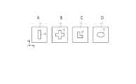
光電子デバイスのさらなる実施形態では、光学構造は、それぞれが、操作される電磁放射線の波長よりも小さい構造要素を含む。構造要素は、光学構造の構造物表面を形成する。例えば、構造要素は、光学構造の表面上にパターンを形成する。構造要素のサイズは、各方向において操作される電磁放射線の波長よりも小さくなり得る。特に横方向において、構造要素のサイズは波長よりも小さい。これは、操作される電磁放射線が赤外線範囲にある場合、光学構造の構造要素は50μmよりも小さくなり得ることを意味する。操作される電磁放射線が赤外線範囲にある場合、光学構造の構造要素は780nmよりも小さくなり得る。操作される電磁放射線が可視スペクトル内にある場合、光学構造の構造要素をさらに小さくなり得る。In a further embodiment of the optoelectronic device, the optical structure includes structural elements each smaller than the wavelength of the electromagnetic radiation to be manipulated. The structural elements form a structure surface of the optical structure. For example, the structural elements form a pattern on the surface of the optical structure. The size of the structural elements can be smaller than the wavelength of the electromagnetic radiation to be manipulated in each direction. In particular in the lateral direction, the size of the structural elements is smaller than the wavelength. This means that if the electromagnetic radiation to be manipulated is in the infrared range, the structural elements of the optical structure can be smaller than 50 μm. If the electromagnetic radiation to be manipulated is in the infrared range, the structural elements of the optical structure can be smaller than 780 nm. If the electromagnetic radiation to be manipulated is in the visible spectrum, the structural elements of the optical structure can be even smaller.
上面図では、構造要素の形状は任意であり、用途によって決まる。上面図は、横断方向において基板とは反対側に面している光学構造の側面からの光電子デバイスの図を指す。上面図の構造要素の形状は、電磁放射線が所望の方法で光学構造と相互作用するように設計される。電磁放射線の相互作用は、回折、屈折、位相遅延等によって発生する可能性がある。In the top view, the shape of the structural elements is arbitrary and depends on the application. The top view refers to a view of the optoelectronic device from the side of the optical structure facing away from the substrate in the transverse direction. The shape of the structural elements in the top view is designed to cause electromagnetic radiation to interact with the optical structure in a desired manner. Electromagnetic radiation interaction can occur through diffraction, refraction, phase delay, etc.
有利には、電磁放射線の波長よりも小さい構造要素を含む光学構造により、振幅、位相、分散、運動量、及び偏光に関して光特性を完全に制御することが可能である。構造要素の正確な形状、ジオメトリ、サイズ、向き、及び配置により、波をブロック、吸収、増強、または曲げることによって、様々な方法で電磁波を操作することが可能な特性が与えられる。そのような光学構造により、例えば、サブ波長グレーティング、偏光子、バイナリレンズ等の多様な光学素子を製造できる。Advantageously, optical structures containing structural elements smaller than the wavelength of electromagnetic radiation allow complete control over optical properties in terms of amplitude, phase, dispersion, momentum, and polarization. The precise shape, geometry, size, orientation, and placement of the structural elements impart properties that allow the electromagnetic waves to be manipulated in various ways by blocking, absorbing, enhancing, or bending the waves. Such optical structures allow the fabrication of a wide variety of optical elements, such as, for example, subwavelength gratings, polarizers, binary lenses, etc.
光電子デバイスのさらなる実施形態では、光学構造はメタマテリアルを含む。メタマテリアルは、自然発生の材料には見られない特性を有するように設計された材料である。これは、電磁波の伝播特性が動作波長よりもはるかに小さい特徴サイズを有するこれらの材料の構造によって主に定義される材料によって実現できる。これは、メタマテリアルが構成要素の特性からではなく、設計された構造及び形状から特性を導出することを意味する。別の実施形態では、光学構造はメタ表面を含む。メタ表面は、メタマテリアルの2次元の等価物であり、非常に薄い層の離散的なサブ波長構造で構成される。In a further embodiment of the optoelectronic device, the optical structure comprises a metamaterial. A metamaterial is a material designed to have properties not found in naturally occurring materials. This can be achieved by materials where the electromagnetic wave propagation properties are defined primarily by the structure of these materials, with feature sizes much smaller than the operating wavelength. This means that metamaterials derive their properties from the designed structure and geometry, not from the properties of the components. In another embodiment, the optical structure comprises a metasurface. A metasurface is the two-dimensional equivalent of a metamaterial, composed of discrete sub-wavelength structures in very thin layers.
有利には、メタマテリアル及びメタ表面は、バルク材では観察されない方法で電磁放射線の波に影響を与える可能性がある。例えば、メタマテリアルは、複素屈折率の負の実部を有し得る。メタマテリアルまたはメタ表面を含む光学構造により、光電子デバイス内の電磁放射線の伝播を完全に制御することが可能である。Advantageously, metamaterials and metasurfaces can affect electromagnetic radiation waves in ways not observed in bulk materials. For example, metamaterials can have a negative real part of the complex refractive index. Optical structures including metamaterials or metasurfaces can provide complete control over the propagation of electromagnetic radiation within optoelectronic devices.
光電子デバイスのさらなる実施形態では、光学構造は、レンズ、回折格子、ゾーンプレート、位相板、ホログラフィックプレート、及び拡散板を含むグループの1つの要素を形成する。レンズが光学構造によって形成される場合、レンズは、例えば、屈折レンズ、フレネルレンズ、またはマイクロレンズ等の任意の従来のレンズであり得る。これは、レンズを形成する光学構造が曲面を有し得ることを意味する。しかしながら、別の実施形態では、レンズはバイナリレンズである。これは、光学構造が、パターンを形成する構造物表面を有することを意味する。これは、カバー層とは反対側に面している光学構造の側面が凹部を有し得ることを意味する。他の実施形態では、光学構造は、回折格子、ゾーンプレート、またはホログラフィックプレートを形成する。これは、光学構造が構造物表面を伴う層によって形成されることを意味する。カバー層とは反対側に面している光学構造の側面が凹部を有し得る。これらの凹部は、規則的または不規則なパターンを形成し得る。光学構造が位相板または拡散板を形成する場合、光学構造の表面は、基板の主延長面に平行であり得る。In a further embodiment of the optoelectronic device, the optical structure forms one element of the group comprising a lens, a diffraction grating, a zone plate, a phase plate, a holographic plate, and a diffuser. If a lens is formed by the optical structure, the lens may be any conventional lens, such as, for example, a refractive lens, a Fresnel lens, or a microlens. This means that the optical structure forming the lens may have a curved surface. However, in another embodiment, the lens is a binary lens. This means that the optical structure has a structure surface that forms a pattern. This means that the side of the optical structure facing away from the cover layer may have recesses. In other embodiments, the optical structure forms a diffraction grating, a zone plate, or a holographic plate. This means that the optical structure is formed by a layer with a structure surface. The side of the optical structure facing away from the cover layer may have recesses. These recesses may form a regular or irregular pattern. If the optical structure forms a phase plate or a diffuser, the surface of the optical structure may be parallel to the main extension plane of the substrate.
有利には、光学構造は、任意の所望の光学素子を形成できる。このように、光電子デバイスは、例えば、ビーム成形、ビームステアリング、またはホログラフィの用途のような複数の用途に使用できる。Advantageously, the optical structures can form any desired optical element. In this way, optoelectronic devices can be used in multiple applications, such as, for example, beam shaping, beam steering, or holographic applications.
光電子デバイスのさらなる実施形態では、光学構造は、焦点距離、偏向角、位相遅延、光偏光、及びパターン投影を含むグループの要素である目標仕様を含む。光学構造の目標仕様は、少なくとも1つの調整構造内の電場を制御することによって変更される。光学構造は、独立型光学素子である。これは、光学構造が、調整構造、または調整構造に印加された電場とは独立した目標仕様を含むことを意味する。例えば、光学構造は、入射電磁放射線を集束、偏向、または拡散するために提供される。他の実施形態では、入射電磁放射線を遅延または偏光させるために光学構造が提供される。さらに他の実施形態では、光学構造は、入射電磁放射線を使用して、分析される対象物に光パターンを投影するために、すなわち、構造化された光を生成するために提供される。しかしながら、調整構造に電場を印加することによって、光学構造の目標仕様が変更される。これは、調整構造が電磁放射線の入力波面を修正するためであり、その結果、この修正された波面が光学構造を通過するとき、結果について、光学構造の元の目標仕様との偏差が制御されたものになる。例えば、調整構造は、それを通過する光を局所的に遅延させる。この局所的遅延は、特定の光学構造に合わせて設計できる。電場を印加及び/または変更すると、光学構造の2つ以上の目標仕様にも影響を与える可能性がある。In a further embodiment of the optoelectronic device, the optical structure includes target specifications that are members of the group including focal length, deflection angle, phase delay, light polarization, and pattern projection. The target specifications of the optical structure are altered by controlling the electric field in at least one adjustment structure. The optical structure is a stand-alone optical element. This means that the optical structure includes target specifications that are independent of the adjustment structure or the electric field applied to the adjustment structure. For example, the optical structure is provided to focus, deflect, or diffuse the incident electromagnetic radiation. In other embodiments, the optical structure is provided to retard or polarize the incident electromagnetic radiation. In yet other embodiments, the optical structure is provided to use the incident electromagnetic radiation to project a light pattern onto an object to be analyzed, i.e., to generate structured light. However, by applying an electric field to the adjustment structure, the target specifications of the optical structure are altered. This is because the adjustment structure modifies the input wavefront of the electromagnetic radiation, so that when this modified wavefront passes through the optical structure, the result has a controlled deviation from the original target specifications of the optical structure. For example, the adjustment structure locally retards the light passing through it. This localized retardation can be engineered for a particular optical structure. Applying and/or modifying the electric field can also affect two or more target specifications of the optical structure.
有利には、光学構造の目標仕様を動的に変更できる。これは、例えば、検出対象の物体が動作中に移動するカメラ用途で役立つ。したがって、焦点の変更が可能である。これは、さらに、走査用途のように、放射光が異なる方向に向けられる発光システムに役立つ。その上、光学構造の目標仕様の調整機能により、光電子デバイスを較正でき、製造変動を補償できる。Advantageously, the target specifications of the optical structure can be dynamically changed. This is useful, for example, in camera applications where the object to be detected moves during operation. Thus, the focus can be changed. This is also useful for light emitting systems where the emitted light is directed in different directions, such as in scanning applications. Moreover, the ability to adjust the target specifications of the optical structure allows the optoelectronic device to be calibrated and manufacturing variations to be compensated for.
光電子デバイスのさらなる実施形態では、上面図で、調整構造は円周部を含む。これは、調整構造の円周部をリングとして、もしくはフレームとして、またはリングもしくはフレームの一部として形成できることを意味する。上面図では、円周部は、調整構造がない内側領域を囲んでいる。円周部は、連続的または不連続的であり得る。後者の場合、円周部にギャップがあり得る。これは、円周部が分割リングを形成できることを意味する。有利には、調整構造の円周部の形状は、それを通過する電磁放射線を局所的に操作することを可能にする。In a further embodiment of the optoelectronic device, in a top view, the adjustment structure comprises a circumferential portion. This means that the circumferential portion of the adjustment structure can be formed as a ring or as a frame or as part of a ring or frame. In a top view, the circumferential portion surrounds an inner area where there is no adjustment structure. The circumferential portion can be continuous or discontinuous. In the latter case, there can be gaps in the circumferential portion. This means that the circumferential portion can form a split ring. Advantageously, the shape of the circumferential portion of the adjustment structure makes it possible to locally manipulate the electromagnetic radiation passing through it.
光電子デバイスのさらなる実施形態では、上面図で、少なくとも1つの別の調整構造は、少なくとも1つの別の円周部を含み、少なくとも1つの別の円周部は、横方向において円周部を囲む。これは、少なくとも1つの別の円周部が円周部よりも大きい直径を有することを意味する。別の調整構造は、サイズを除いて調整構造と同じ設定または特性を有し得る。ある実施形態では、光電子デバイスは複数の調整構造を含む。複数の調整構造は、それぞれ、少なくとも1つの別の円周部を含む。しかしながら、複数の調整構造は、それぞれ、2つ以上の別の円周部も含み得る。異なる調整構造の後ろに位置する別の円周部の直径は増加できる。これは、後ろに位置する別の円周部が横方向に前に位置する別の円周部を囲むことができることを意味する。しかしながら、別の円周部は互いに隣り合わせて配置され得るため、これらの円周部は、もう1つの別の円周部がない各々の内側領域を囲む。少なくとも1つの別の円周部は、連続的または不連続的であり得る。後者の場合、別の円周部にギャップがあり得る。これは、別の円周部が分割リングを形成できることを意味する。別の円周部の量及びそれらの互いに対する正確な配置は、所望の調整範囲に依存する。In a further embodiment of the optoelectronic device, in a top view, the at least one further adjustment structure includes at least one further circumferential portion, which laterally surrounds the circumferential portion. This means that the at least one further circumferential portion has a larger diameter than the circumferential portion. The further adjustment structure may have the same settings or characteristics as the adjustment structure, except for the size. In an embodiment, the optoelectronic device includes a plurality of adjustment structures. The plurality of adjustment structures each includes at least one further circumferential portion. However, the plurality of adjustment structures may each also include two or more further circumferential portions. The diameter of the further circumferential portions located behind the different adjustment structures can be increased. This means that the further circumferential portion located behind can laterally surround the further circumferential portion located in front. However, the further circumferential portions may be arranged next to each other, so that these circumferential portions surround each inner area where there is no other further circumferential portion. The at least one further circumferential portion may be continuous or discontinuous. In the latter case, there may be gaps in the further circumferential portion. This means that separate circumferential sections can form a split ring. The amount of separate circumferential sections and their exact location relative to each other depends on the desired adjustment range.
有利には、調整構造、または調整構造の一部は、空間的に局所化された調整構造を個々に調整できるように、リングまたはフレームとして配置できる。これにより、例えば、調整可能なレンズとして、異なる適用シナリオで光電子デバイスを使用することが可能である。Advantageously, the adjustment structure, or parts of the adjustment structure, can be arranged as a ring or frame, such that the spatially localized adjustment structures can be individually adjusted. This makes it possible to use the optoelectronic device in different application scenarios, for example as an adjustable lens.
さらなる実施形態では、光電子デバイスは、調整構造のアレイを形成する複数の調整構造を含む。調整構造のアレイは、規則的または不規則なグリッドを形成できる。上面図では、調整構造のアレイの要素である各調整構造は、長方形の形状を有し得る。しかしながら、各々の調整構造の多角形または円形も可能である。調整構造の量及び互いに対して正確な配置は、所望の調整範囲によって決まる。In a further embodiment, the optoelectronic device includes a plurality of adjustment structures forming an array of adjustment structures. The array of adjustment structures can form a regular or irregular grid. In top view, each adjustment structure that is an element of the array of adjustment structures can have a rectangular shape. However, polygonal or circular shapes of each adjustment structure are also possible. The amount of adjustment structures and their exact placement relative to each other depends on the desired tuning range.
有利には、調整構造は、空間的に局所化された調整構造を個々に調整できるように、アレイまたはマトリックスとして配置できる。これにより、例えば、ビームステアリング用途及びホログラフィで、異なる適用シナリオで光電子デバイスを使用することが可能である。Advantageously, the adjustment structures can be arranged in an array or matrix, such that spatially localized adjustment structures can be individually adjusted. This allows the optoelectronic device to be used in different application scenarios, for example in beam steering applications and in holography.
光電子デバイスのさらなる実施形態では、第1の電気接点及び第2の電気接点は、調整構造の各々の側面に配置される。調整構造の側面は、基板の主延長面に対して垂直または横方向に延びる。電気接点の材料が残りの調整構造の材料と直接物理的に接触している側面の領域は、接触エリアを形成する。これは、接触エリアが調整構造の各々の側面に配置されることを意味する。第1電気接点と第2電気接点との間の電位差は、調整構造内に電場をもたらし、その方向は、接触エリアの正確な場所及び電位差の符号に依存する。In a further embodiment of the optoelectronic device, the first electrical contact and the second electrical contact are arranged on each side of the adjustment structure. The side of the adjustment structure extends perpendicularly or laterally to the main extension plane of the substrate. The area of the side where the material of the electrical contact is in direct physical contact with the material of the remaining adjustment structure forms a contact area. This means that the contact area is arranged on each side of the adjustment structure. A potential difference between the first and second electrical contacts results in an electric field in the adjustment structure, the direction of which depends on the exact location of the contact area and the sign of the potential difference.
この配置により、調整構造内の電場を基板の主延長面と平行に向けることが有利に可能である。電場の強さ及び向きは、調整構造の光学特性に影響を与える。This arrangement advantageously allows the electric field in the tuning structure to be oriented parallel to the main extension plane of the substrate. The strength and orientation of the electric field influence the optical properties of the tuning structure.
光電子デバイスのさらなる実施形態では、第1の電気接点及び第2の電気接点は、各々、調整構造の上面及び背面に配置される。上面及び背面は、基板の主延長面と平行に延在する。上面及び背面は、調整構造の反対側に配置される。In a further embodiment of the optoelectronic device, the first electrical contact and the second electrical contact are respectively arranged on a top surface and a back surface of the adjustment structure. The top surface and the back surface extend parallel to a main extension surface of the substrate. The top surface and the back surface are arranged on opposite sides of the adjustment structure.
この配置により、有利には、調整構造内の電場を基板の主延長面に対して横断方向に向けることが有利に可能である。電場の強さ及び向きは、調整構造の光学特性に影響を与える。This arrangement advantageously makes it possible to orient the electric field in the adjustment structure transversely to the main extension plane of the substrate. The strength and orientation of the electric field influence the optical properties of the adjustment structure.
さらなる実施形態では、光電子デバイスは複数の調整構造を含む。電圧源によって生成された電場は、動作中の調整構造のうちの少なくとも2つにおいて異なる。これは、異なる調整構造に各々異なる電場を同時に印加できること、または異なる調整構造が必ずしも同じ電場を示すわけではないことを意味する。電場は強さ及び/または方向が異なり得る。有利には、異なる電場を異なる調整構造に印加することによって、光電子デバイスの光学特性を局所的に変化させることができる。次に、電磁放射線の伝播は、時間だけでなく空間的にも制御できる。In a further embodiment, the optoelectronic device comprises a plurality of tuning structures. The electric field generated by the voltage source is different in at least two of the tuning structures during operation. This means that different electric fields can be applied simultaneously to the different tuning structures, respectively, or that the different tuning structures do not necessarily exhibit the same electric field. The electric fields can differ in strength and/or direction. Advantageously, by applying different electric fields to the different tuning structures, the optical properties of the optoelectronic device can be locally changed. The propagation of the electromagnetic radiation can then be controlled not only in time but also in space.
光電子デバイスのさらなる実施形態では、電圧源によって生成された電場は、少なくとも1つの調整構造における動作中に時間とともに可変である。これは、調整構造内の電場を動作中に動的に変化させることができることを意味する。電場を変化させることで、非常に短い時間スケール内で発生する可能性がある。例えば、調整構造内の電場を変化させることで、数ピコ秒(ps)またはそれ以上の速さで行うことができる。上述のように、電場を変化させることによって、光電子デバイスの光学特性も変化する。有利には、光電子デバイスの光学目標仕様は動的に変更できる。これは、例えば、検出対象の物体が動作中に移動するカメラ用途で役立つ。さらに、電場を非常に短時間領域内で変化させることで、デバイスを通過する電磁放射線を超高速で変調することが可能である。In a further embodiment of the optoelectronic device, the electric field generated by the voltage source is variable over time during operation in at least one adjustment structure. This means that the electric field in the adjustment structure can be dynamically changed during operation. Changing the electric field can occur within a very short time scale. For example, changing the electric field in the adjustment structure can be done as fast as a few picoseconds (ps) or faster. As mentioned above, changing the electric field also changes the optical properties of the optoelectronic device. Advantageously, the optical target specifications of the optoelectronic device can be dynamically changed. This is useful, for example, in camera applications where the object to be detected moves during operation. Furthermore, by changing the electric field within a very short time domain, it is possible to modulate the electromagnetic radiation passing through the device at ultrafast speeds.
光電子デバイスのさらなる実施形態では、操作される電磁放射線は赤外線波長範囲にある。別の実施形態では、操作される電磁放射線は、近赤外波長範囲にある。さらに別の実施形態では、操作される電磁放射線は、近赤外波長範囲にある。さらに別の実施形態では、操作される電磁放射線は、上述の波長範囲の少なくとも2つに重なる範囲にある。基板、調整構造、カバー層、及び光学構造に使用された材料は、各々の波長範囲の電磁放射線に対して透過的である。例えば、操作される電磁放射線が赤外波長範囲にある場合、光電子デバイスの構成要素は、赤外放射に対して透過的な材料を含み得る。操作される電磁放射線が可視波長範囲にある場合、光電子デバイスの構成要素は、可視光に対して透過的な材料を含み得る。調整構造の電気接点は、また、各々の電磁放射線に対して透過的な材料を含み得る。しかしながら、上面図では電気接点の領域が比較的小さくなり得るため、電気接点は電磁放射線に対して透過的でない場合もある。これは、例えば、電気接点が金属を含む場合である。有利には、光電子デバイスは、様々な波長領域に適したものになるように設計できる。これにより、異なる用途で使用することが可能である。In a further embodiment of the optoelectronic device, the electromagnetic radiation to be manipulated is in the infrared wavelength range. In another embodiment, the electromagnetic radiation to be manipulated is in the near infrared wavelength range. In yet another embodiment, the electromagnetic radiation to be manipulated is in the near infrared wavelength range. In yet another embodiment, the electromagnetic radiation to be manipulated is in a range that overlaps at least two of the above-mentioned wavelength ranges. The materials used for the substrate, the adjustment structure, the cover layer, and the optical structure are transparent to the electromagnetic radiation of the respective wavelength range. For example, if the electromagnetic radiation to be manipulated is in the infrared wavelength range, the components of the optoelectronic device may include a material that is transparent to infrared radiation. If the electromagnetic radiation to be manipulated is in the visible wavelength range, the components of the optoelectronic device may include a material that is transparent to visible light. The electrical contacts of the adjustment structure may also include a material that is transparent to the respective electromagnetic radiation. However, the electrical contacts may not be transparent to the electromagnetic radiation, since the area of the electrical contacts may be relatively small in a top view. This is the case, for example, when the electrical contacts include a metal. Advantageously, the optoelectronic device can be designed to be suitable for various wavelength ranges. This allows it to be used for a variety of purposes.
さらなる実施形態では、光電子デバイスは電子システムに含まれる。電子システムは、特に、電磁放射線を放出及び/または感知するために設けられた光電子システムである。ある実施形態では、電子システムは照明器または光源を含む。光源は、例えば、フォトダイオードもしくは垂直キャビティ面発光レーザ(VCSEL)、または各々、フォトダイオードもしくはVCSELのアレイであり得る。電子システムに含まれる光電子デバイスによって、光源によって放出された電磁放射線を操作できる。例えば、電磁放射線は、増幅、遅延、方向付け、偏光等がもたらされ得る。別の実施形態では、電子システムは、電磁放射線用のセンサーまたは検出器を備える。検出器は、フォトダイオード、光電子増倍管(PMT)もしくはサーモパイル、または各々、それらのアレイであり得る。光電子デバイスによって、電子システムに到達する電磁放射線を操作できる。例えば、電磁放射線は、増幅、遅延、方向付け、偏光等がもたらされ得る。In a further embodiment, the optoelectronic device is included in an electronic system. The electronic system is in particular an optoelectronic system arranged to emit and/or sense electromagnetic radiation. In an embodiment, the electronic system includes an illuminator or light source. The light source can be, for example, a photodiode or a vertical cavity surface emitting laser (VCSEL), or an array of photodiodes or VCSELs, respectively. The optoelectronic device included in the electronic system allows the electromagnetic radiation emitted by the light source to be manipulated. For example, the electromagnetic radiation can be amplified, delayed, directed, polarized, etc. In another embodiment, the electronic system includes a sensor or detector for the electromagnetic radiation. The detector can be a photodiode, a photomultiplier tube (PMT) or a thermopile, or an array thereof, respectively. The optoelectronic device allows the electromagnetic radiation reaching the electronic system to be manipulated. For example, the electromagnetic radiation can be amplified, delayed, directed, polarized, etc.
これらの特性により、そのような電子システムは、ビーム形成及びビームステアリングの用途に使用できる。一実施形態では、電子システムはカメラシステムである。例えば、電子システムは3Dカメラであり、構造化された光を使用して、検出対象の物体の深度情報を取得する。特に、光電子システムは、光検出及び測距システム(ライダー)である。別の実施形態では、電子デバイスはホログラム発生器である。さらに別の実施形態では、電子デバイスは携帯電話等のスマートデバイスであり、光電子デバイスは集積光学素子として使用される。光電子デバイスは、微小電気機械システム(MEMS)の技術によって製造できるため、電子システムは小さい寸法を有し得る。These properties allow such electronic systems to be used in beam forming and beam steering applications. In one embodiment, the electronic system is a camera system. For example, the electronic system is a 3D camera that uses structured light to obtain depth information of the object being detected. In particular, the optoelectronic system is a light detection and ranging system (lidar). In another embodiment, the electronic device is a hologram generator. In yet another embodiment, the electronic device is a smart device such as a mobile phone, and the optoelectronic device is used as an integrated optical element. The optoelectronic device can be manufactured by microelectromechanical systems (MEMS) technology, so the electronic system can have small dimensions.
以下の図の説明は、さらに、例示的な実施形態を例示及び説明し得る。機能的に同一または同一の効果をもたらす構成要素は、同一の参照番号で示される。同一または実質的に同一の構成要素は、それらが最初に出現する図だけに関して説明され得る。これらの説明は、連続する図で必ずしも繰り返されるわけではない。The following figure description may further illustrate and explain exemplary embodiments. Components that are functionally identical or provide the same effect are indicated with the same reference numerals. Identical or substantially identical components may be described only with respect to the figure in which they first appear. These descriptions are not necessarily repeated in successive figures.
図1では、光電子デバイス1の実施形態の断面図が示される。図1による実施形態は、主表面3を有する基板2を含む。基板2は主延長面を有する。横方向x,yは、基板2の主延長面と平行に延在する。少なくとも1つの調整構造4が基板2の主表面3に配置される。図1に示される例では、基板2の主表面3に配置される4つの調整構造4がある。横方向x,yにおいて、調整構造4は互いに距離がある。これは、調整構造4が互いに離間していることを意味する。調整構造4は、それぞれ、基板2の主延長面に平行な上面5及び背面6を有する。上面5及び背面6は、調整構造4のそれぞれの反対側に配置される。調整構造4のそれぞれの背面6は基板2に面している。上面5は、基板2とは反対側に面している。In FIG. 1, a cross-sectional view of an embodiment of an optoelectronic device 1 is shown. The embodiment according to FIG. 1 comprises a
調整構造4のそれぞれは、第1の電気接点7及び第2の電気接点8を含む。電気接点7、8は、残りの調整構造4と比較して異なる材料を含む。図1に示される実施形態では、第1の電気接点7は調整構造4の上面5に配置される。第2の電気接点8は、調整構造4の背面6に配置される。電気接点7、8は、各々、上面5の全体を覆う、または背面6の全体を覆う。しかしながら、他の実施形態では、電気接点7、8は、調整構造4の各々の表面5、6の一部だけを覆う。図1に示される実施形態では、調整構造4の側面9は、第1の電気接点7及び第2の電気接点8がない。これは、第1の電気接点7及び第2の電気接点8が互いに物理的または電気的に接続されていないことを意味する。Each of the adjustment structures 4 includes a first
図1による光電子デバイス1は、さらに、カバー層10を含む。カバー層10は、基板2と同じ材料を含み得る。しかしながら、カバー層10は、また、異なる材料を含み得る。カバー層10は、基板2に面する背面6を除いて、少なくとも1つの調整構造4をその全ての側面で覆う。しかしながら、電気接点7、8はそれでもアクセス可能である。少なくとも1つの調整構造4がない領域上で、カバー層10は基板2と直接接触している。カバー層10は上面11を有する。上面11は、基板2の主延長面と平行に延在し得る。The optoelectronic device 1 according to FIG. 1 further comprises a
カバー層10の上面11には、光学構造12が配置される。基板2の主延長面に垂直な横断方向zにおいて、光学構造12は調整構造4の上にある。カバー層10は、調整構造4と光学構造12との間に配置される。図1に示される実施形態では、光学構造12は、複数の構造要素13を含む。これは、光学構造12が、パターンを形成する構造物表面21を有することを意味する。パターンは、一方の側では凹部14によって形成され、他方の側では構造要素13によって形成される。横断方向Zでは、光学構造12は厚みを有する。図1に示されるように、凹部14が光学構造12の全厚にわたって延在するため、カバー層10の上面11の一部は露出される。これは、光学構造12の構造要素13が互いに離されていることを意味する。しかしながら、図5~図7は、下記に説明される光学構造の異なる概念を示す。On the
図1に示されるように、光電子デバイス1は、さらに、電圧源15を備える。電圧源15は、示されるように、外部電圧源15であり得る。しかしながら、電圧源15は、また、基板2に統合できる。電圧源15は、少なくとも1つの調整構造4の第1の電気接点7及び第2の電気接点8に電気的に接続される。提示する目的のために、調整構造4の1つだけが図1の電圧源15に接続される。しかしながら、調整構造4のそれぞれは、同じ電圧源15または別の電圧源15に接続され得る。電圧源15は、第1の電気接点7と第2の電気接点8との間に電位差を生成するために提供される。次に、これにより、少なくとも1つの調整要素4内に電場が生成される。電源15から第1の電気接点7及び第2の電気接点8までの電気接続は、導電性ワイヤ16によって実現される。導電性ワイヤ16は、電気接点と同じ材料または異なる材料を含み得る。導電性ワイヤ16は、図1に示されるように、基板2及びカバー層10に統合できる。電気接点7、8は、導電性ワイヤを介してアクセス可能であり得る。As shown in FIG. 1, the optoelectronic device 1 further comprises a
動作中、電磁放射線は、3つの矢印によって示されるように、基板2の背面17に到達する。その後、電磁放射線は、基板2、調整構造4、及びカバー層10を通過し、光学構造12に到達する。光学構造12は、所定の方法で電磁放射線を操作する。光学構造12は、例えば、焦点距離、偏向角等によって電磁放射線を操作する目標仕様を有する。調整構造4に電場を印加することによって、電磁放射線の入力波面は、例えば、位相遅延によって修正されるため、修正された波面が光学構造12を通過するとき、結果は、光学構造12の元の目標仕様との偏差が制御されたものになる。In operation, electromagnetic radiation reaches the
図2A~図2Dは、光学構造12の構造要素13の異なる実施形態を上面図で示す。上面図は、基板2とは反対側に面するカバー層10の側面からの光電子デバイス1の図を指す。図2A~図2Dは、カバー層10の上面11に配置された各々の構造要素13のうちの1つの詳細だけを示す。他の構造要素までの長さ、幅、及び距離は、特に、操作される電磁放射線の波長よりも小さくなり得る。2A-2D show different embodiments of the
図2Aは、長方形の形状を有する構造要素13を示し、y方向の構造要素の寸法を指す長さは、x方向の構造要素の寸法を指す幅よりも大きい。しかしながら、構造要素13の割合は、また、等しくなり得る、または、置き換えられ得る。さらに、そのような構造要素13は、横方向x,yに回転できる。横方向x,yにおける構造要素13の向きは、隣接する構造要素13の向きに対して等しくなり得るまたは異なり得る。Figure 2A shows a
図2Bは、プラス形状を有するカバー層10の上にある構造要素13を示す。前述の実施形態と同様に、そのような構造要素13は横方向x,yに回転できる。横方向x,yにおける構造要素13の向きは、隣接する構造要素13の向きに対して等しくなり得るまたは異なり得る。Figure 2B shows a
図2Cは、L字型を有するカバー層10の上にある構造要素13を示す。前述の実施形態と同様に、そのような構造要素13は横方向x,yに回転できる。横方向x,yにおける構造要素13の向きは、隣接する構造要素13の向きに対して等しくなり得るまたは異なり得る。Figure 2C shows a
図2Dは、上面図において湾曲形状を有する、カバー層10の上にある構造要素13を示す。本実施形態では、構造要素13は楕円を形成する。しかしながら、例えば、円について、任意の他の湾曲形状も可能である。Figure 2D shows a
構造要素13の示される実施形態の全てが互いに組み合わせることができるため、構造要素13のうちの少なくとも2つが異なる形状を含むようになることに留意されたい。Please note that all of the illustrated embodiments of
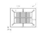
図3には、光電子デバイス1の別の実施形態の上面図が示される。この場合、光電子デバイス1は、基板2及びカバー層10を含み、これらは上面図において円形を有する。光電子デバイス1の調整構造4は、円周部18を含む。この場合、円周部18は、基板2上にリングを形成する。円周部18によって形成されたリングは直径を有し、調整構造4のない領域を囲む。別の調整構造4’は、別の円周部19を含む。別の円周部19は、円周部18よりも大きい直径を有し、横方向x,yにおいて円周部18を囲む。一方の側では、別の円周部はギャップを含む。これは、別の円周部19が分割リングを形成することを意味する。3 shows a top view of another embodiment of an optoelectronic device 1. In this case, the optoelectronic device 1 comprises a
調整構造4及び別の調整構造4’は、また、第1の電気接点7を含む。上述のように、第1の電気接点7は、各々の調整構造4、4’の上面5に配置され、これは、図3の観察者に向かって面する調整構造4、4’の側面を意味する。調整構造4及び別の調整構造4’は、また、各々の調整構造4、4’の背面6に配置される第2の電気接点8を含む。これは、調整構造4、4’の側面に、図3の観察者とは反対側を向いていることを意味する。図3では、第2の電気接点8が第1の電気接点7の下に正確に横断方向zに配置できることを示すために、第2の電気接点8は破線によって描かれる。その結果、斜視図の観察者から見えなくなる。The adjustment structure 4 and the further adjustment structure 4' also include a first
円周部18を含む調整構造4の第1の電気接点7及び第2の電気接点8は、それらが横方向yに円周部18から別の円周部19のギャップを通って光電子デバイス1の周辺領域に到達するように配置される。光電子デバイス1の周辺領域は、調整構造の上に光学構造が存在しないため、光学的に不活性である領域を指す。別の円周部19を含む別の調整構造4’の第1の電気接点7及び第2の電気接点8は、任意の横方向x,yにおいて、別の円周部19から周辺領域に到達する。この配置により、調整構造4、4’のそれぞれの第1の電気接点7及び第2の電気接点8はアクセス可能であり、光電子デバイス1の周辺領域で電圧源15(図示せず)に接続できる。The first
図3に示される実施形態は、上面図において円形を有する構造要素13を含む光学構造12を含む。上面図では、光学構造12によって覆われた全エリアは、円周部18及び別の円周部19によって横方向x,yにおいて囲まれたエリアにほぼ一致する。このエリアは、光学活性エリアと呼ばれ得る。3 includes an
図3に示される実施形態では、光学構造12は、調整可能なメタレンズ、すなわちメタマテリアルを含むレンズを形成するために提供できる。メタレンズは、光学活性エリアに対応する直径を有する。調整構造4及び別の調整構造4’は、メタレンズによって既に実装されている位相関数に補正を導入する。調整構造4、4’のそれぞれの電気接点7、8が別々に配置されるため、各々の調整構造4、4’は電場によって独立して制御できる。このように、必要に応じてレンズの直径に沿って異なる位相遅延を実現できる。In the embodiment shown in FIG. 3, the
図4に示される光電子デバイスの実施形態は、上面図で長方形の形状を有する、基板2及びカバー層10を含む。本実施形態は、さらに、アレイとして配置される複数の調整構造4を含むという点で、図3の実施形態とは異なる。この場合、アレイは6つの調整構造4を含む。図4では、調整構造4のそれぞれの第1の電気接点7だけが示される。しかしながら、第2の電気接点8(図示せず)は、第1の電気接点7の真下に配置できるため、観察者の視点からは見えない。電気接点7、8は、横方向x,yに、各々の調整構造4から光電子デバイス1の異なる周辺領域に向かって延在している。このように、それらは1つ以上の電圧源15(図示せず)に別々に接続できる。次に、これにより、調整構造4のそれぞれに電場を独立して制御することが可能になる。The embodiment of the optoelectronic device shown in FIG. 4 includes a
光学構造12は、調整構造4のアレイの上に横断方向zに配置される。横方向x,yにおいて構造要素13を含む光学構造12によって覆われるエリアは、調整構造4のアレイによって覆われたエリアとほぼ同じ大きさであり得る。しかしながら、図4に示されるように、調整構造4のアレイによって覆われた全エリアは、光学構造12によって覆われたエリアよりもわずかに大きくなり得る。両方のエリアの重なり合う領域は、光学活性エリアと呼ばれ得る。The
図5に示される光電子デバイス1の実施形態は、異なる光学構造12を示すという点で、図1に示される実施形態とは異なる。図5の光学構造12は、また、カバー層10とは反対側に面する構造物表面21を含む。しかしながら、構造要素13は、凹部14が光学構造12の全厚にわたって延在しないので、互いに物理的に接続される。したがって、カバー層10の上面11の一部は、光学構造12が存在するエリアで露出されない。これは、カバー層10が光学構造12によって完全に覆われていることを意味する。構造物表面21は、規則的または不規則的であり得るパターンを形成する。構造要素13は、図2a~図2dに従った形状を含み得る。別の実施形態では、構造要素13は、光学活性エリアにわたって同心リングを形成する。この場合、光学構造12は、ゾーンプレートまたはバイナリレンズを形成する。The embodiment of the optoelectronic device 1 shown in FIG. 5 differs from the embodiment shown in FIG. 1 in that it shows a different
図5は、少なくとも1つの調整構造4に電気的に接触するための異なる概念を示すという点で、図1とはさらに異なる。この場合、調整構造4のそれぞれは、調整構造4の側面9または別の側面9’に各々配置された、第1の電気接点7及び第2の電気接点8を有する。側面9及び別の側面9’は、基板2の主延長面に対して垂直または横方向に延びる。第1の電気接点7が配置される側面9は、第2の電気接点が配置される別の側面9’から分離される。このように、第1の電気接点7及び第2の電気接点8は、互いに電気的に絶縁される。図5に示されるように、第1の電気接点7及び第2の電気接点8は、調整構造4の各々の側面9,9’の全体を覆うことができる。5 further differs from FIG. 1 in that it shows a different concept for electrically contacting at least one adjustment structure 4. In this case, each of the adjustment structures 4 has a first
図6に示される光電子デバイス1の実施形態は、異なる光学構造12の別の変形を示すという点で、図5に示される実施形態とは異なる。この場合、光学構造12は、平面21を伴う層を形成する。これは、カバー層10とは反対側に面する光学構造12の表面21が、基板2の主延長面と平行に延びることを意味する。光学構造12が位相板または拡散板を形成する場合、光学構造12のこの実施形態を使用できる。The embodiment of the optoelectronic device 1 shown in FIG. 6 differs from the embodiment shown in FIG. 5 in that it shows another variant of a different
図7に示される光電子デバイス1の実施形態は、異なる光学構造12の別の変形を示すという点で、図6に示される実施形態とは異なる。この場合、光学構造12は曲面21を有する。これは、カバー層10とは反対側に面する光学構造12の表面21が、基板2の主延長面に対して曲率を示すことを意味する。光学構造12が屈折レンズを形成する場合、光学構造12のこの実施形態を使用できる。The embodiment of the optoelectronic device 1 shown in FIG. 7 differs from the embodiment shown in FIG. 6 in that it shows another variant of a different
図8は、シミュレーションによって得られた関数のグラフを示す。ここで、電磁放射線の強度Iは、光学構造12と、光学構造12の上の横断方向zの位置との間の距離dに対してプロットされる。強度IはW/m2の単位で与えられる。距離dはμmの単位で与えられる。 8 shows a graph of the function obtained by simulation, where the intensity I of the electromagnetic radiation is plotted against the distance d between the
この場合、光学構造12は、例えば、図3に関連して説明したようなレンズを形成する。シミュレーションの結果は、レンズを形成する光学構造12の焦点距離を見つけるために使用できる。しかしながら、光学構造12の任意の他の目標仕様も同様の方法で分析できることに留意されたい。In this case, the
3つの異なるシナリオの強度特性が示される。第1のシナリオ(曲線22)は、調整構造4に電場が印加されていない間の電磁放射線の強度Iを示す。第2のシナリオ及び第3のシナリオ(曲線23及び曲線24)は、各々の電場が整調構造4に印加される間の電磁放射線の強度Iを示す。曲線22は、約35μmで明確な最大値を示す。これは、光学構造12の焦点距離がこの距離で識別できることを意味する。また、シミュレーション結果として示されるものとして、光電子デバイス1は、光学構造12によって、調整なしでも、すなわち電場を印加することによって調整モードではない動作モードにおいて、目標仕様が示される。しかしながら、特定の強さ及び方向の電場を印加することによって、最大強度は約45μmの距離dだけシフトする(曲線23)。さらに、曲線24によって示されるように異なる電場を印加することによって、最大強度を反対方向、すなわち約25μmの距離dまでシフトできる。これは、光電子デバイス1の光学特性が、各々の電場を印加することによっていずれかの方向に動的に変化できることを意味する。The intensity characteristics of three different scenarios are shown. The first scenario (curve 22) shows the intensity I of the electromagnetic radiation while no electric field is applied to the tuning structure 4. The second and third scenarios (
本明細書に開示される光電子デバイス1の実施形態は、読者が発想の新規の態様を知ることを目的として説明されてきた。好ましい実施形態が示され説明されてきたが、当業者は、特許請求の範囲から不必要に逸脱することなく、開示された概念の多くの変更、修正、同等物、及び置換がなされ得る。The embodiments of the optoelectronic device 1 disclosed herein have been described with the objective of acquainting the reader with novel aspects of the concept. While preferred embodiments have been shown and described, those skilled in the art may make numerous variations, modifications, equivalents, and substitutions of the disclosed concepts without unnecessarily departing from the scope of the claims.
本開示は、開示された実施形態、及び上記で具体的に示され、説明されたものに限定されないことを理解されたい。むしろ、別個の従属請求項または明細書に記載された特徴は有利に組み合わされ得る。さらに、本開示の範囲は、当業者には明らかであり、添付の特許請求の範囲に含まれるそれらの変形及び修正を含む。It is to be understood that the present disclosure is not limited to the disclosed embodiments and those specifically shown and described above. Rather, features described in separate dependent claims or in the specification may be advantageously combined. Moreover, the scope of the present disclosure includes those variations and modifications that are obvious to those skilled in the art and that are included within the scope of the appended claims.
「含む(comprising)」という用語は、特許請求の範囲または発明を実施するための形態で使用される限り、対応する特徴または手順の他の要素またはステップを除外しない。「a」または「an」という用語が特徴に関連して使用される場合、それらの用語は複数のそのような特徴を除外しない。さらに、特許請求の範囲におけるいずれかの参照符号は、範囲を限定するものと解釈するべきではない。The term "comprising", when used in a claim or description, does not exclude other elements or steps of the corresponding feature or procedure. When the terms "a" or "an" are used in connection with a feature, they do not exclude a plurality of such features. Moreover, any reference signs in the claims should not be construed as limiting the scope.
この特許出願は、欧州出願特許第20172735.1号の優先権を主張し、その開示の内容は、参照により本明細書に組み込まれる。This patent application claims priority to European Patent Application No. 20172735.1, the disclosure of which is incorporated herein by reference.
1 光電子デバイス
2 基板
3 基板の主表面
4 調整構造
4’ 別の調整構造
5 調整構造の上面
6 調整構造の背面
7 第1の電気接点
8 第2の電気接点
9 調整構造の側面
9’ 調整構造の別の側面
10 カバー層
11 カバー層の上面
12 光学構造
13 光学構造の構造要素
14 光学構造の凹部
15 電圧源
16 導電性ワイヤ
17 基板の背面
18 調整構造の円周部
19 別の外周部
20 別の円周部のギャップ
21 光学構造の表面
22 関数グラフの第1の曲線
23 関数グラフの第2の曲線
24 関数グラフの第3の曲線
x,y 横方向
z 横断方向
d 光学構造までの距離 1
Claims (15)
Translated fromJapanese主延長面を有する基板(2)と、
前記基板(2)の主表面(3)上に配置された少なくとも1つの調整構造(4)であって、前記調整構造(4)は電気光学材料を含み、前記少なくとも1つの調整構造(4)は、前記調整構造(4)の第1の側にある第1の電気接点(7)と、前記調整構造(4)の第2の側にある第2の電気接点(8)とを含む、前記少なくとも1つの調整構造(4)と、
前記少なくとも1つの調整構造(4)を覆うカバー層(10)と、
前記カバー層(10)が光学構造(12)と前記少なくとも1つの調整構造(4)との間に配置されるように、前記カバー層(10)上に配置された光学構造(12)と、
前記第1の電気接点(7)及び前記第2の電気接点(8)に電気的に接続された電圧源(15)であって、前記少なくとも1つの調整構造(4)内に電場を生成するために設けられる、前記電圧源(15)と、
を含み、
前記光学構造(12)は、目標仕様を有し、前記目標仕様は、焦点距離、偏向角、位相遅延、光偏光、及びパターン投影のうちの少なくとも1つを含み、
前記光学構造(12)の前記目標仕様は、前記少なくとも1つの調整構造(4)内の前記電場を制御することによって変更される、光電子デバイス(1)。 An optoelectronic device (1) for manipulating electromagnetic radiation, comprising:
A substrate (2) having a main extension surface;
at least one adjustment structure (4) arranged on a main surface (3) of the substrate (2), the adjustment structure (4) comprising an electro-optical material, the at least one adjustment structure (4) comprising a first electrical contact (7) on a first side of the adjustment structure (4) and a second electrical contact (8) on a second side of the adjustment structure (4);
a cover layer (10) covering said at least one adjustment structure (4);
an optical structure (12) disposed on the cover layer (10) such that the cover layer (10) is disposed between the optical structure (12) and the at least one adjustment structure (4);
a voltage source (15) electrically connected to the first electrical contact (7) and the second electrical contact (8), the voltage source (15) being provided for generating an electric field within the at least one adjustment structure (4);
Including,
the optical structure (12)has target specifications, the target specificationsincludingat least one of a focal length, a deflection angle, a phase delay, a light polarization, and a pattern projection;
An optoelectronic device (1), wherein the target specification of the optical structure (12) is altered by controlling the electric field in the at least one tuning structure (4).
Applications Claiming Priority (3)
| Application Number | Priority Date | Filing Date | Title |
|---|---|---|---|
| EP20172735.1AEP3907536A1 (en) | 2020-05-04 | 2020-05-04 | Manipulating electromagnetic radiation |
| EP20172735.1 | 2020-05-04 | ||
| PCT/EP2021/061301WO2021224108A1 (en) | 2020-05-04 | 2021-04-29 | Manipulating electromagnetic radiation |
Publications (2)
| Publication Number | Publication Date |
|---|---|
| JP2023523158A JP2023523158A (en) | 2023-06-02 |
| JP7526809B2true JP7526809B2 (en) | 2024-08-01 |
Family
ID=70553757
Family Applications (1)
| Application Number | Title | Priority Date | Filing Date |
|---|---|---|---|
| JP2022560947AActiveJP7526809B2 (en) | 2020-05-04 | 2021-04-29 | Manipulation of electromagnetic radiation |
Country Status (7)
| Country | Link |
|---|---|
| US (1) | US20230161075A1 (en) |
| EP (1) | EP3907536A1 (en) |
| JP (1) | JP7526809B2 (en) |
| KR (1) | KR102737237B1 (en) |
| CN (1) | CN115485589B (en) |
| DE (1) | DE112021002589T5 (en) |
| WO (1) | WO2021224108A1 (en) |
Families Citing this family (3)
| Publication number | Priority date | Publication date | Assignee | Title |
|---|---|---|---|---|
| EP4523009A2 (en)* | 2022-05-11 | 2025-03-19 | Lumotive, Inc. | Tunable optical devices with integrated electronics |
| US11487184B1 (en) | 2022-05-11 | 2022-11-01 | Lumotive, LLC | Integrated driver and self-test control circuitry in tunable optical devices |
| DE102023125990A1 (en)* | 2023-09-26 | 2025-03-27 | Ams-Osram International Gmbh | OPTOELECTRONIC MODULE |
Citations (9)
| Publication number | Priority date | Publication date | Assignee | Title |
|---|---|---|---|---|
| JP2006293018A (en) | 2005-04-11 | 2006-10-26 | Rohm Co Ltd | Optical modulation apparatus and system |
| JP2006301630A (en) | 2005-04-15 | 2006-11-02 | Asml Netherlands Bv | Variable lens and exposure system |
| US20080151168A1 (en) | 2006-12-21 | 2008-06-26 | Citizen Watch Co., Ltd. | Liquid-crystal optical element, camera using the same, and optical pickup device using the same |
| US20130128334A1 (en) | 2011-11-18 | 2013-05-23 | Vuzix Corporation | Beam Steering Device |
| CN204129398U (en) | 2014-11-05 | 2015-01-28 | 华中科技大学 | A kind of infrared optically focused chip |
| US20150146116A1 (en) | 2013-11-28 | 2015-05-28 | Shenzhen China Star Optoelectronics Technology Co., Ltd. | Display device and liquid crystal prism cell panel |
| WO2017057700A1 (en) | 2015-10-01 | 2017-04-06 | 国立大学法人東京大学 | Optical modulator and optical modulation device |
| JP2019086765A (en) | 2017-11-08 | 2019-06-06 | 三星電子株式会社Samsung Electronics Co.,Ltd. | Projector including metal lens |
| JP2021051293A (en) | 2019-09-23 | 2021-04-01 | 三星電子株式会社Samsung Electronics Co.,Ltd. | Optical modulator and beam steering system comprising the same |
Family Cites Families (6)
| Publication number | Priority date | Publication date | Assignee | Title |
|---|---|---|---|---|
| GB2369896A (en)* | 2000-12-06 | 2002-06-12 | Marconi Comm Ltd | Tunable optical filter actuator |
| EP1785991A4 (en)* | 2004-08-04 | 2009-01-07 | Asahi Glass Co Ltd | LIQUID CRYSTAL LENS ELEMENT AND OPTICAL HEAD |
| CN104765205B (en)* | 2014-12-30 | 2018-07-20 | 厦门天马微电子有限公司 | A kind of array substrate, display panel and display device |
| KR102754868B1 (en)* | 2016-11-16 | 2025-01-14 | 삼성전자주식회사 | Two dimensionally light modulating device and electronic apparatus including the same |
| KR102464367B1 (en)* | 2017-01-10 | 2022-11-07 | 삼성전자주식회사 | Optical modulating device and system employing the same |
| CN110994091A (en)* | 2019-12-13 | 2020-04-10 | 华南理工大学 | Terahertz tunable filter based on super surface |
- 2020
- 2020-05-04EPEP20172735.1Apatent/EP3907536A1/ennot_activeWithdrawn
- 2021
- 2021-04-29DEDE112021002589.9Tpatent/DE112021002589T5/enactivePending
- 2021-04-29JPJP2022560947Apatent/JP7526809B2/enactiveActive
- 2021-04-29CNCN202180032477.6Apatent/CN115485589B/enactiveActive
- 2021-04-29KRKR1020227042105Apatent/KR102737237B1/enactiveActive
- 2021-04-29USUS17/922,900patent/US20230161075A1/enactivePending
- 2021-04-29WOPCT/EP2021/061301patent/WO2021224108A1/ennot_activeCeased
Patent Citations (9)
| Publication number | Priority date | Publication date | Assignee | Title |
|---|---|---|---|---|
| JP2006293018A (en) | 2005-04-11 | 2006-10-26 | Rohm Co Ltd | Optical modulation apparatus and system |
| JP2006301630A (en) | 2005-04-15 | 2006-11-02 | Asml Netherlands Bv | Variable lens and exposure system |
| US20080151168A1 (en) | 2006-12-21 | 2008-06-26 | Citizen Watch Co., Ltd. | Liquid-crystal optical element, camera using the same, and optical pickup device using the same |
| US20130128334A1 (en) | 2011-11-18 | 2013-05-23 | Vuzix Corporation | Beam Steering Device |
| US20150146116A1 (en) | 2013-11-28 | 2015-05-28 | Shenzhen China Star Optoelectronics Technology Co., Ltd. | Display device and liquid crystal prism cell panel |
| CN204129398U (en) | 2014-11-05 | 2015-01-28 | 华中科技大学 | A kind of infrared optically focused chip |
| WO2017057700A1 (en) | 2015-10-01 | 2017-04-06 | 国立大学法人東京大学 | Optical modulator and optical modulation device |
| JP2019086765A (en) | 2017-11-08 | 2019-06-06 | 三星電子株式会社Samsung Electronics Co.,Ltd. | Projector including metal lens |
| JP2021051293A (en) | 2019-09-23 | 2021-04-01 | 三星電子株式会社Samsung Electronics Co.,Ltd. | Optical modulator and beam steering system comprising the same |
Also Published As
| Publication number | Publication date |
|---|---|
| US20230161075A1 (en) | 2023-05-25 |
| JP2023523158A (en) | 2023-06-02 |
| KR20230003217A (en) | 2023-01-05 |
| KR102737237B1 (en) | 2024-12-02 |
| CN115485589A (en) | 2022-12-16 |
| WO2021224108A1 (en) | 2021-11-11 |
| CN115485589B (en) | 2024-06-21 |
| EP3907536A1 (en) | 2021-11-10 |
| DE112021002589T5 (en) | 2023-02-16 |
Similar Documents
| Publication | Publication Date | Title |
|---|---|---|
| JP7526809B2 (en) | Manipulation of electromagnetic radiation | |
| US9709829B2 (en) | Beam steering device | |
| US10856057B2 (en) | Optical device and methods | |
| US11340513B2 (en) | SAW modulators and light steering methods | |
| CN108627974A (en) | Photo-scanning system | |
| JPWO2018061515A1 (en) | Optical scanning device, optical receiving device, and optical detection system | |
| CN118938561A (en) | Optical scanning device | |
| JPWO2018061514A1 (en) | Optical scanning device, optical receiving device, and optical detection system | |
| JP5742141B2 (en) | Optical scanning device | |
| CN110446972B (en) | Optical scanning device, optical receiving device, and optical detection system | |
| US12135405B2 (en) | Electrically-controlled dynamic optical component comprising a planar metasurface | |
| JP2018128663A (en) | Optical scanning device, optical receiving device, and optical detection system | |
| WO2019130721A1 (en) | Optical device | |
| US20170131475A1 (en) | Infrared scene projector with per-pixel spectral and polarisation capability | |
| WO2023231859A1 (en) | Liquid crystal device, and optical modulation device and system | |
| WO2018061231A1 (en) | Optical scan device, optical reception device, and waveguide array | |
| US8089677B2 (en) | Dynamic optical grating device and associated method for modulating light | |
| JP7028456B2 (en) | Optical deflection element, drive method of optical deflection element, and optical deflection element module | |
| US11480836B2 (en) | Liquid crystal on silicon device with microlens | |
| CN104849860B (en) | A kind of system for removing laser light field coherence | |
| WO2025037445A1 (en) | Optical modulation device, optical observation device, and light irradiation device | |
| KR20240074400A (en) | Vr module using metasurface |
Legal Events
| Date | Code | Title | Description |
|---|---|---|---|
| A521 | Request for written amendment filed | Free format text:JAPANESE INTERMEDIATE CODE: A523 Effective date:20221202 | |
| A621 | Written request for application examination | Free format text:JAPANESE INTERMEDIATE CODE: A621 Effective date:20221202 | |
| A977 | Report on retrieval | Free format text:JAPANESE INTERMEDIATE CODE: A971007 Effective date:20230914 | |
| A131 | Notification of reasons for refusal | Free format text:JAPANESE INTERMEDIATE CODE: A131 Effective date:20230926 | |
| A131 | Notification of reasons for refusal | Free format text:JAPANESE INTERMEDIATE CODE: A131 Effective date:20240305 | |
| A521 | Request for written amendment filed | Free format text:JAPANESE INTERMEDIATE CODE: A523 Effective date:20240603 | |
| TRDD | Decision of grant or rejection written | ||
| A01 | Written decision to grant a patent or to grant a registration (utility model) | Free format text:JAPANESE INTERMEDIATE CODE: A01 Effective date:20240702 | |
| A61 | First payment of annual fees (during grant procedure) | Free format text:JAPANESE INTERMEDIATE CODE: A61 Effective date:20240722 | |
| R150 | Certificate of patent or registration of utility model | Ref document number:7526809 Country of ref document:JP Free format text:JAPANESE INTERMEDIATE CODE: R150 |