JP7525752B1 - Ceramic showerhead with conductive electrodes - Google Patents
Ceramic showerhead with conductive electrodesDownload PDFInfo
- Publication number
- JP7525752B1 JP7525752B1JP2024054295AJP2024054295AJP7525752B1JP 7525752 B1JP7525752 B1JP 7525752B1JP 2024054295 AJP2024054295 AJP 2024054295AJP 2024054295 AJP2024054295 AJP 2024054295AJP 7525752 B1JP7525752 B1JP 7525752B1
- Authority
- JP
- Japan
- Prior art keywords
- showerhead
- conductive material
- apertures
- manufacturing
- processing system
- Prior art date
- Legal status (The legal status is an assumption and is not a legal conclusion. Google has not performed a legal analysis and makes no representation as to the accuracy of the status listed.)
- Active
Links
Images


Classifications
- H—ELECTRICITY
- H01—ELECTRIC ELEMENTS
- H01J—ELECTRIC DISCHARGE TUBES OR DISCHARGE LAMPS
- H01J37/00—Discharge tubes with provision for introducing objects or material to be exposed to the discharge, e.g. for the purpose of examination or processing thereof
- H01J37/32—Gas-filled discharge tubes
- H01J37/32431—Constructional details of the reactor
- H01J37/32458—Vessel
- H01J37/32477—Vessel characterised by the means for protecting vessels or internal parts, e.g. coatings
- H01J37/32495—Means for protecting the vessel against plasma
- C—CHEMISTRY; METALLURGY
- C23—COATING METALLIC MATERIAL; COATING MATERIAL WITH METALLIC MATERIAL; CHEMICAL SURFACE TREATMENT; DIFFUSION TREATMENT OF METALLIC MATERIAL; COATING BY VACUUM EVAPORATION, BY SPUTTERING, BY ION IMPLANTATION OR BY CHEMICAL VAPOUR DEPOSITION, IN GENERAL; INHIBITING CORROSION OF METALLIC MATERIAL OR INCRUSTATION IN GENERAL
- C23C—COATING METALLIC MATERIAL; COATING MATERIAL WITH METALLIC MATERIAL; SURFACE TREATMENT OF METALLIC MATERIAL BY DIFFUSION INTO THE SURFACE, BY CHEMICAL CONVERSION OR SUBSTITUTION; COATING BY VACUUM EVAPORATION, BY SPUTTERING, BY ION IMPLANTATION OR BY CHEMICAL VAPOUR DEPOSITION, IN GENERAL
- C23C16/00—Chemical coating by decomposition of gaseous compounds, without leaving reaction products of surface material in the coating, i.e. chemical vapour deposition [CVD] processes
- C23C16/22—Chemical coating by decomposition of gaseous compounds, without leaving reaction products of surface material in the coating, i.e. chemical vapour deposition [CVD] processes characterised by the deposition of inorganic material, other than metallic material
- C23C16/30—Deposition of compounds, mixtures or solid solutions, e.g. borides, carbides, nitrides
- C23C16/34—Nitrides
- C—CHEMISTRY; METALLURGY
- C23—COATING METALLIC MATERIAL; COATING MATERIAL WITH METALLIC MATERIAL; CHEMICAL SURFACE TREATMENT; DIFFUSION TREATMENT OF METALLIC MATERIAL; COATING BY VACUUM EVAPORATION, BY SPUTTERING, BY ION IMPLANTATION OR BY CHEMICAL VAPOUR DEPOSITION, IN GENERAL; INHIBITING CORROSION OF METALLIC MATERIAL OR INCRUSTATION IN GENERAL
- C23C—COATING METALLIC MATERIAL; COATING MATERIAL WITH METALLIC MATERIAL; SURFACE TREATMENT OF METALLIC MATERIAL BY DIFFUSION INTO THE SURFACE, BY CHEMICAL CONVERSION OR SUBSTITUTION; COATING BY VACUUM EVAPORATION, BY SPUTTERING, BY ION IMPLANTATION OR BY CHEMICAL VAPOUR DEPOSITION, IN GENERAL
- C23C16/00—Chemical coating by decomposition of gaseous compounds, without leaving reaction products of surface material in the coating, i.e. chemical vapour deposition [CVD] processes
- C23C16/44—Chemical coating by decomposition of gaseous compounds, without leaving reaction products of surface material in the coating, i.e. chemical vapour deposition [CVD] processes characterised by the method of coating
- C23C16/4401—Means for minimising impurities, e.g. dust, moisture or residual gas, in the reaction chamber
- C23C16/4404—Coatings or surface treatment on the inside of the reaction chamber or on parts thereof
- C—CHEMISTRY; METALLURGY
- C23—COATING METALLIC MATERIAL; COATING MATERIAL WITH METALLIC MATERIAL; CHEMICAL SURFACE TREATMENT; DIFFUSION TREATMENT OF METALLIC MATERIAL; COATING BY VACUUM EVAPORATION, BY SPUTTERING, BY ION IMPLANTATION OR BY CHEMICAL VAPOUR DEPOSITION, IN GENERAL; INHIBITING CORROSION OF METALLIC MATERIAL OR INCRUSTATION IN GENERAL
- C23C—COATING METALLIC MATERIAL; COATING MATERIAL WITH METALLIC MATERIAL; SURFACE TREATMENT OF METALLIC MATERIAL BY DIFFUSION INTO THE SURFACE, BY CHEMICAL CONVERSION OR SUBSTITUTION; COATING BY VACUUM EVAPORATION, BY SPUTTERING, BY ION IMPLANTATION OR BY CHEMICAL VAPOUR DEPOSITION, IN GENERAL
- C23C16/00—Chemical coating by decomposition of gaseous compounds, without leaving reaction products of surface material in the coating, i.e. chemical vapour deposition [CVD] processes
- C23C16/44—Chemical coating by decomposition of gaseous compounds, without leaving reaction products of surface material in the coating, i.e. chemical vapour deposition [CVD] processes characterised by the method of coating
- C23C16/455—Chemical coating by decomposition of gaseous compounds, without leaving reaction products of surface material in the coating, i.e. chemical vapour deposition [CVD] processes characterised by the method of coating characterised by the method used for introducing gases into reaction chamber or for modifying gas flows in reaction chamber
- C23C16/45563—Gas nozzles
- C23C16/45565—Shower nozzles
- C—CHEMISTRY; METALLURGY
- C23—COATING METALLIC MATERIAL; COATING MATERIAL WITH METALLIC MATERIAL; CHEMICAL SURFACE TREATMENT; DIFFUSION TREATMENT OF METALLIC MATERIAL; COATING BY VACUUM EVAPORATION, BY SPUTTERING, BY ION IMPLANTATION OR BY CHEMICAL VAPOUR DEPOSITION, IN GENERAL; INHIBITING CORROSION OF METALLIC MATERIAL OR INCRUSTATION IN GENERAL
- C23C—COATING METALLIC MATERIAL; COATING MATERIAL WITH METALLIC MATERIAL; SURFACE TREATMENT OF METALLIC MATERIAL BY DIFFUSION INTO THE SURFACE, BY CHEMICAL CONVERSION OR SUBSTITUTION; COATING BY VACUUM EVAPORATION, BY SPUTTERING, BY ION IMPLANTATION OR BY CHEMICAL VAPOUR DEPOSITION, IN GENERAL
- C23C16/00—Chemical coating by decomposition of gaseous compounds, without leaving reaction products of surface material in the coating, i.e. chemical vapour deposition [CVD] processes
- C23C16/44—Chemical coating by decomposition of gaseous compounds, without leaving reaction products of surface material in the coating, i.e. chemical vapour deposition [CVD] processes characterised by the method of coating
- C23C16/455—Chemical coating by decomposition of gaseous compounds, without leaving reaction products of surface material in the coating, i.e. chemical vapour deposition [CVD] processes characterised by the method of coating characterised by the method used for introducing gases into reaction chamber or for modifying gas flows in reaction chamber
- C23C16/45563—Gas nozzles
- C23C16/45574—Nozzles for more than one gas
- C—CHEMISTRY; METALLURGY
- C23—COATING METALLIC MATERIAL; COATING MATERIAL WITH METALLIC MATERIAL; CHEMICAL SURFACE TREATMENT; DIFFUSION TREATMENT OF METALLIC MATERIAL; COATING BY VACUUM EVAPORATION, BY SPUTTERING, BY ION IMPLANTATION OR BY CHEMICAL VAPOUR DEPOSITION, IN GENERAL; INHIBITING CORROSION OF METALLIC MATERIAL OR INCRUSTATION IN GENERAL
- C23C—COATING METALLIC MATERIAL; COATING MATERIAL WITH METALLIC MATERIAL; SURFACE TREATMENT OF METALLIC MATERIAL BY DIFFUSION INTO THE SURFACE, BY CHEMICAL CONVERSION OR SUBSTITUTION; COATING BY VACUUM EVAPORATION, BY SPUTTERING, BY ION IMPLANTATION OR BY CHEMICAL VAPOUR DEPOSITION, IN GENERAL
- C23C16/00—Chemical coating by decomposition of gaseous compounds, without leaving reaction products of surface material in the coating, i.e. chemical vapour deposition [CVD] processes
- C23C16/44—Chemical coating by decomposition of gaseous compounds, without leaving reaction products of surface material in the coating, i.e. chemical vapour deposition [CVD] processes characterised by the method of coating
- C23C16/458—Chemical coating by decomposition of gaseous compounds, without leaving reaction products of surface material in the coating, i.e. chemical vapour deposition [CVD] processes characterised by the method of coating characterised by the method used for supporting substrates in the reaction chamber
- C23C16/4581—Chemical coating by decomposition of gaseous compounds, without leaving reaction products of surface material in the coating, i.e. chemical vapour deposition [CVD] processes characterised by the method of coating characterised by the method used for supporting substrates in the reaction chamber characterised by material of construction or surface finish of the means for supporting the substrate
- C—CHEMISTRY; METALLURGY
- C23—COATING METALLIC MATERIAL; COATING MATERIAL WITH METALLIC MATERIAL; CHEMICAL SURFACE TREATMENT; DIFFUSION TREATMENT OF METALLIC MATERIAL; COATING BY VACUUM EVAPORATION, BY SPUTTERING, BY ION IMPLANTATION OR BY CHEMICAL VAPOUR DEPOSITION, IN GENERAL; INHIBITING CORROSION OF METALLIC MATERIAL OR INCRUSTATION IN GENERAL
- C23C—COATING METALLIC MATERIAL; COATING MATERIAL WITH METALLIC MATERIAL; SURFACE TREATMENT OF METALLIC MATERIAL BY DIFFUSION INTO THE SURFACE, BY CHEMICAL CONVERSION OR SUBSTITUTION; COATING BY VACUUM EVAPORATION, BY SPUTTERING, BY ION IMPLANTATION OR BY CHEMICAL VAPOUR DEPOSITION, IN GENERAL
- C23C16/00—Chemical coating by decomposition of gaseous compounds, without leaving reaction products of surface material in the coating, i.e. chemical vapour deposition [CVD] processes
- C23C16/44—Chemical coating by decomposition of gaseous compounds, without leaving reaction products of surface material in the coating, i.e. chemical vapour deposition [CVD] processes characterised by the method of coating
- C23C16/50—Chemical coating by decomposition of gaseous compounds, without leaving reaction products of surface material in the coating, i.e. chemical vapour deposition [CVD] processes characterised by the method of coating using electric discharges
- H—ELECTRICITY
- H01—ELECTRIC ELEMENTS
- H01J—ELECTRIC DISCHARGE TUBES OR DISCHARGE LAMPS
- H01J37/00—Discharge tubes with provision for introducing objects or material to be exposed to the discharge, e.g. for the purpose of examination or processing thereof
- H01J37/32—Gas-filled discharge tubes
- H01J37/32431—Constructional details of the reactor
- H01J37/3244—Gas supply means
- H—ELECTRICITY
- H01—ELECTRIC ELEMENTS
- H01J—ELECTRIC DISCHARGE TUBES OR DISCHARGE LAMPS
- H01J37/00—Discharge tubes with provision for introducing objects or material to be exposed to the discharge, e.g. for the purpose of examination or processing thereof
- H01J37/32—Gas-filled discharge tubes
- H01J37/32431—Constructional details of the reactor
- H01J37/32532—Electrodes
- H01J37/32559—Protection means, e.g. coatings
- H—ELECTRICITY
- H01—ELECTRIC ELEMENTS
- H01L—SEMICONDUCTOR DEVICES NOT COVERED BY CLASS H10
- H01L21/00—Processes or apparatus adapted for the manufacture or treatment of semiconductor or solid state devices or of parts thereof
- H01L21/02—Manufacture or treatment of semiconductor devices or of parts thereof
- H01L21/04—Manufacture or treatment of semiconductor devices or of parts thereof the devices having potential barriers, e.g. a PN junction, depletion layer or carrier concentration layer
- H01L21/18—Manufacture or treatment of semiconductor devices or of parts thereof the devices having potential barriers, e.g. a PN junction, depletion layer or carrier concentration layer the devices having semiconductor bodies comprising elements of Group IV of the Periodic Table or AIIIBV compounds with or without impurities, e.g. doping materials
- H01L21/28—Manufacture of electrodes on semiconductor bodies using processes or apparatus not provided for in groups H01L21/20 - H01L21/268
- H01L21/283—Deposition of conductive or insulating materials for electrodes conducting electric current
- H01L21/285—Deposition of conductive or insulating materials for electrodes conducting electric current from a gas or vapour, e.g. condensation
- H01L21/28506—Deposition of conductive or insulating materials for electrodes conducting electric current from a gas or vapour, e.g. condensation of conductive layers
- H01L21/28512—Deposition of conductive or insulating materials for electrodes conducting electric current from a gas or vapour, e.g. condensation of conductive layers on semiconductor bodies comprising elements of Group IV of the Periodic Table
- H—ELECTRICITY
- H01—ELECTRIC ELEMENTS
- H01L—SEMICONDUCTOR DEVICES NOT COVERED BY CLASS H10
- H01L21/00—Processes or apparatus adapted for the manufacture or treatment of semiconductor or solid state devices or of parts thereof
- H01L21/02—Manufacture or treatment of semiconductor devices or of parts thereof
- H01L21/04—Manufacture or treatment of semiconductor devices or of parts thereof the devices having potential barriers, e.g. a PN junction, depletion layer or carrier concentration layer
- H01L21/18—Manufacture or treatment of semiconductor devices or of parts thereof the devices having potential barriers, e.g. a PN junction, depletion layer or carrier concentration layer the devices having semiconductor bodies comprising elements of Group IV of the Periodic Table or AIIIBV compounds with or without impurities, e.g. doping materials
- H01L21/30—Treatment of semiconductor bodies using processes or apparatus not provided for in groups H01L21/20 - H01L21/26
- H01L21/302—Treatment of semiconductor bodies using processes or apparatus not provided for in groups H01L21/20 - H01L21/26 to change their surface-physical characteristics or shape, e.g. etching, polishing, cutting
- H01L21/306—Chemical or electrical treatment, e.g. electrolytic etching
- H01L21/3065—Plasma etching; Reactive-ion etching
- H—ELECTRICITY
- H01—ELECTRIC ELEMENTS
- H01L—SEMICONDUCTOR DEVICES NOT COVERED BY CLASS H10
- H01L21/00—Processes or apparatus adapted for the manufacture or treatment of semiconductor or solid state devices or of parts thereof
- H01L21/02—Manufacture or treatment of semiconductor devices or of parts thereof
- H01L21/04—Manufacture or treatment of semiconductor devices or of parts thereof the devices having potential barriers, e.g. a PN junction, depletion layer or carrier concentration layer
- H01L21/18—Manufacture or treatment of semiconductor devices or of parts thereof the devices having potential barriers, e.g. a PN junction, depletion layer or carrier concentration layer the devices having semiconductor bodies comprising elements of Group IV of the Periodic Table or AIIIBV compounds with or without impurities, e.g. doping materials
- H01L21/30—Treatment of semiconductor bodies using processes or apparatus not provided for in groups H01L21/20 - H01L21/26
- H01L21/31—Treatment of semiconductor bodies using processes or apparatus not provided for in groups H01L21/20 - H01L21/26 to form insulating layers thereon, e.g. for masking or by using photolithographic techniques; After treatment of these layers; Selection of materials for these layers
- H01L21/3205—Deposition of non-insulating-, e.g. conductive- or resistive-, layers on insulating layers; After-treatment of these layers
- H01L21/321—After treatment
- H01L21/3213—Physical or chemical etching of the layers, e.g. to produce a patterned layer from a pre-deposited extensive layer
- H—ELECTRICITY
- H01—ELECTRIC ELEMENTS
- H01L—SEMICONDUCTOR DEVICES NOT COVERED BY CLASS H10
- H01L21/00—Processes or apparatus adapted for the manufacture or treatment of semiconductor or solid state devices or of parts thereof
- H01L21/67—Apparatus specially adapted for handling semiconductor or electric solid state devices during manufacture or treatment thereof; Apparatus specially adapted for handling wafers during manufacture or treatment of semiconductor or electric solid state devices or components ; Apparatus not specifically provided for elsewhere
- H01L21/67005—Apparatus not specifically provided for elsewhere
- H01L21/67011—Apparatus for manufacture or treatment
- H01L21/67017—Apparatus for fluid treatment
- H01L21/67063—Apparatus for fluid treatment for etching
- H01L21/67069—Apparatus for fluid treatment for etching for drying etching
Landscapes
- Chemical & Material Sciences (AREA)
- Engineering & Computer Science (AREA)
- Physics & Mathematics (AREA)
- Plasma & Fusion (AREA)
- Organic Chemistry (AREA)
- Metallurgy (AREA)
- Mechanical Engineering (AREA)
- Materials Engineering (AREA)
- Chemical Kinetics & Catalysis (AREA)
- General Chemical & Material Sciences (AREA)
- Analytical Chemistry (AREA)
- Power Engineering (AREA)
- Microelectronics & Electronic Packaging (AREA)
- Computer Hardware Design (AREA)
- Manufacturing & Machinery (AREA)
- General Physics & Mathematics (AREA)
- Condensed Matter Physics & Semiconductors (AREA)
- Inorganic Chemistry (AREA)
- Drying Of Semiconductors (AREA)
- Chemical Vapour Deposition (AREA)
- Plasma Technology (AREA)
- Formation Of Insulating Films (AREA)
Abstract
Translated fromJapanese
Description
Translated fromJapanese 関連出願の相互参照
[0001]本出願は、2019年1月11日に出願された米国特許出願第16/245,698号に対する優先権の利益を主張するものであり、その内容を、参照により本明細書に援用する。 CROSS-REFERENCE TO RELATED APPLICATIONS [0001] This application claims the benefit of priority to U.S. patent application Ser. No. 16/245,698, filed Jan. 11, 2019, the contents of which are incorporated herein by reference.
[0002]本技術は、半導体プロセス及び機器に関する。より具体的には、本技術は、システム電極として動作し得るセラミックチャンバ構成要素に関する。[0002] The present technology relates to semiconductor processes and equipment. More specifically, the present technology relates to ceramic chamber components that can act as system electrodes.
[0003]集積回路は、基板表面に複雑にパターニングされた材料層を製造するプロセスによって可能になる。基板にパターニングされた材料を製造するには、露出した材料を除去するための制御された方法が必要である。化学エッチングは、フォトレジストのパターンを下にある層に転写する、層を薄くする、又は表面にすでに存在する特徴の横方向の寸法を薄くすることを含む、様々な目的で使用される。多くの場合、ある材料を別の材料よりも速くエッチングして、例えば、パターン転写プロセスを容易にするエッチングプロセスを有することが望ましい。このようなエッチングプロセスは、第1の材料に対して選択的であると言われる。材料、回路、及びプロセスの多様性の結果として、エッチングプロセスは、様々な材料に対して選択性を有するように開発されてきた。[0003] Integrated circuits are made possible by processes that fabricate intricately patterned layers of material on a substrate surface. Fabricating patterned materials on a substrate requires a controlled method for removing exposed material. Chemical etching is used for a variety of purposes, including transferring a pattern in a photoresist to an underlying layer, thinning a layer, or thinning the lateral dimensions of features already present on a surface. It is often desirable to have an etching process that etches one material faster than another, for example, to facilitate the pattern transfer process. Such an etching process is said to be selective to the first material. As a result of the diversity of materials, circuits, and processes, etching processes have been developed that are selective to a variety of materials.
[0004]エッチングプロセスは、プロセスで使用される材料に基づいて、ウェット又はドライと呼ばれ得る。例えば、ウェットエッチングは、他の誘電体及び材料よりも幾つかの酸化物誘電体を優先的に除去し得る。ただし、ウェットプロセスでは、狭いトレンチに浸透するのが困難な場合があり、残りの材料が変形する場合もある。基板処理領域内に形成されたプラズマで生じるドライエッチングは、より狭いトレンチに浸透し、繊細な残りの構造の変形を減らし得る。ただし、プラズマが、放電時の電気アークの発生だけでなく、システム構成要素への衝撃及びエッチングを通して、基板又はチャンバの構成要素に損傷を与え得る。[0004] Etch processes may be referred to as wet or dry based on the materials used in the process. For example, wet etches may preferentially remove some oxide dielectrics over other dielectrics and materials. However, wet processes may have difficulty penetrating narrow trenches and may distort the remaining material. Dry etches, which occur with a plasma formed within the substrate processing region, may penetrate narrower trenches and reduce distortion of delicate remaining structures. However, plasmas may damage the substrate or chamber components through bombardment and etching of system components as well as the generation of electrical arcs during discharge.
[0005]したがって、高品質の装置及び構造を製造するために使用可能な改善されたシステム及び方法が必要である。これら及び他の必要性は、本技術によって対処される。[0005] Thus, there is a need for improved systems and methods that can be used to manufacture high quality devices and structures. These and other needs are addressed by the present technology.
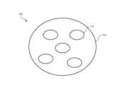
[0006]例示的な半導体処理チャンバのシャワーヘッドは、第1の面と、第1の面の反対側の第2の面とによって特徴付けられる誘電体プレートを含み得る。誘電体プレートは、誘電体プレートを通る複数の開孔を画定し得る。誘電体プレートは、誘電体プレートの第1の面に第1の環状チャネルを画定し得、第1の環状チャネルは、複数の開孔の周りに延在し得る。誘電体プレートは、誘電体プレートの第1の面に第2の環状チャネルを画定し得る。第2の環状チャネルは、第1の環状チャネルから半径方向外側に形成され得る。シャワーヘッドはまた、誘電体プレート内に埋め込まれ、開孔によって露出されずに複数の開孔の周りに延在する導電性材料も含み得る。導電性材料は、第2の環状チャネルで露出され得る。[0006] An exemplary semiconductor processing chamber showerhead may include a dielectric plate characterized by a first surface and a second surface opposite the first surface. The dielectric plate may define a plurality of apertures through the dielectric plate. The dielectric plate may define a first annular channel in the first surface of the dielectric plate, the first annular channel may extend around the plurality of apertures. The dielectric plate may define a second annular channel in the first surface of the dielectric plate. The second annular channel may be formed radially outward from the first annular channel. The showerhead may also include a conductive material embedded within the dielectric plate and extending around the plurality of apertures without being exposed by the apertures. The conductive material may be exposed at the second annular channel.
[0007]幾つかの実施形態では、第2の環状チャネルは、誘電体プレート内で、第1の環状チャネルよりも深い深さまで画定され得る。導電性材料は、第1の環状チャネルの深さよりも深い誘電体プレート内の深さで誘電体プレートを通って延在し得る。導電性材料は、第1の環状チャネルによって露出されずに第2の環状チャネルによって露出され得る。シャワーヘッドはまた、第2の環状チャネル内に着座し、導電性材料を電極として動作させるように構成されたRFガスケットも含み得る。シャワーヘッドはまた、第1の環状チャネル内に着座したエラストマー要素も含み得る。導電性材料は、第1の環状チャネルによって画定される、シャワーヘッドの内部領域全体に延在するフォイル(foil)又はメッシュを含み得る。導電性材料は、シャワーヘッドの内部領域から第2の環状チャネルまで延在する複数のタブを含み得る。[0007] In some embodiments, the second annular channel may be defined in the dielectric plate to a depth greater than that of the first annular channel. The conductive material may extend through the dielectric plate at a depth in the dielectric plate greater than that of the first annular channel. The conductive material may be exposed by the second annular channel without being exposed by the first annular channel. The showerhead may also include an RF gasket seated in the second annular channel and configured to operate the conductive material as an electrode. The showerhead may also include an elastomeric element seated in the first annular channel. The conductive material may include a foil or mesh extending throughout an interior region of the showerhead defined by the first annular channel. The conductive material may include a plurality of tabs extending from an interior region of the showerhead to the second annular channel.
[0008]本技術の幾つかの実施形態はまた、第1の誘電体材料を含むプレートを含み得る半導体処理チャンバのシャワーヘッドも包含し得る。プレートは、第1の面と、第1の面の反対側の第2の面とによって特徴づけられ得る。プレートは、プレートを通る複数の開孔を画定し得る。シャワーヘッドは、プレートの第1の面に配置された導電性材料を含み得、導電性材料は、複数の開孔の各開孔から第1の半径方向の距離に維持され得る。シャワーヘッドはまた、第2の誘電体材料を含むコーティングも含み得る。コーティングは、導電性材料全体に延在し得、コーティングは、複数の開孔の各開孔から第2の半径方向の距離に維持され得る。第2の半径方向の距離が第1の半径方向の距離よりも短くてよい。[0008] Some embodiments of the present technology may also include a showerhead for a semiconductor processing chamber that may include a plate including a first dielectric material. The plate may be characterized by a first side and a second side opposite the first side. The plate may define a plurality of apertures through the plate. The showerhead may include a conductive material disposed on the first side of the plate, the conductive material may be maintained a first radial distance from each aperture of the plurality of apertures. The showerhead may also include a coating including a second dielectric material. The coating may extend throughout the conductive material, and the coating may be maintained a second radial distance from each aperture of the plurality of apertures. The second radial distance may be less than the first radial distance.
[0009]幾つかの実施形態では、導電性材料は、シャワーヘッドの電気的結合を提供するために、シャワーヘッドの半径方向のエッジで露出され得る。シャワーヘッドは、プレートの第1の面において、複数の開孔の半径方向外側、及びシャワーヘッドの半径方向のエッジで露出された導電性材料の半径方向内側に環状チャネルを画定し得る。コーティングは、多層コーティングであり得る、又はそれを含み得る。第1の誘電体材料及び第2の誘電体材料は、異なる材料であり得る、又は異なる材料を含み得る。導電性材料は、有孔フォイル又はメッシュであり得る、又はそれを含み得る。[0009] In some embodiments, the conductive material may be exposed at a radial edge of the showerhead to provide electrical coupling to the showerhead. The showerhead may define an annular channel in the first surface of the plate radially outward of the plurality of apertures and radially inward of the conductive material exposed at the radial edge of the showerhead. The coating may be or may include a multi-layer coating. The first dielectric material and the second dielectric material may be or may include different materials. The conductive material may be or may include a perforated foil or mesh.
[0010]本技術の幾つかの実施形態は、リッドと基板支持体とを有する半導体処理チャンバを包含し得る。チャンバはまた、リッドと基板支持体との間に位置づけされたシャワーヘッドも含み得る。第1のプラズマ領域が、シャワーヘッドとリッドとの間に画定され得、第2のプラズマ領域が、シャワーヘッドと基板支持体との間に画定され得る。リッドと基板支持体とがそれぞれプラズマ生成電源に結合され得る。シャワーヘッドは、電気的に接地されていてよく、シャワーヘッドは、第1の誘電体プレートを含むプレートを含み得る。プレートは、第1の面と、第1の面の反対側の第2の面とによって特徴付けられ得る。プレートは、プレートを通る複数の開孔を画定し得、シャワーヘッドは、プレートの第1の面において、複数の開孔の半径方向外側に第1の環状チャネルを画定し得る。シャワーヘッドはまた、プレートに組み込まれた導電性材料も含み得る。導電性材料の露出は、第1の環状チャネルの半径方向外側の領域に限定され得る。[0010] Some embodiments of the present technology may include a semiconductor processing chamber having a lid and a substrate support. The chamber may also include a showerhead positioned between the lid and the substrate support. A first plasma region may be defined between the showerhead and the lid, and a second plasma region may be defined between the showerhead and the substrate support. The lid and the substrate support may each be coupled to a plasma generating power source. The showerhead may be electrically grounded, and may include a plate including a first dielectric plate. The plate may be characterized by a first surface and a second surface opposite the first surface. The plate may define a plurality of apertures therethrough, and the showerhead may define a first annular channel in the first surface of the plate radially outward of the plurality of apertures. The showerhead may also include a conductive material incorporated in the plate. Exposure of the conductive material may be limited to a region radially outward of the first annular channel.
[0011]幾つかの実施形態では、プレートは、プレートの第1の面に第2の環状チャネルを画定し得る。第2の環状チャネルは、第1の環状チャネルから半径方向外側に形成され得、導電性材料は、プレート内に埋め込まれ、第2の環状チャネルによって露出され得る。第2の環状チャネルは、プレート内で第1の環状チャネルよりも深い深さまで画定され得る。導電性材料は、第1の環状チャネルの深さよりも深いプレート内の深さでプレートを通って延在し得る。導電性材料は、第1の環状チャネルによって露出されずに第2の環状チャネルによって露出され得る。処理チャンバはまた、第2の環状チャネル内に着座し、導電性材料を電気的に接地するように構成されたRFガスケットも含み得る。チャンバはまた、第1の環状チャネル内に着座したエラストマー要素も含み得る。導電性材料は、プレートの第1の面に配置され得、導電性材料は、複数の開孔の各開孔から第1の半径方向の距離に維持され得る。シャワーヘッドはまた、第2の誘電体材料であり得るコーティングも含み得る。コーティングは、導電性材料全体に延在し得、コーティングは、複数の開孔の各開孔から第2の半径方向の距離に維持され得る。第2の半径方向の距離は、第1の半径方向の距離よりも短くてよい。コーティングは、多層コーティングであり得る、又はそれを含み得る。導電性材料は、有孔フォイル又はメッシュであり得る、又はそれを含み得る。[0011] In some embodiments, the plate may define a second annular channel in a first surface of the plate. The second annular channel may be formed radially outward from the first annular channel, and the conductive material may be embedded in the plate and exposed by the second annular channel. The second annular channel may be defined in the plate to a depth greater than that of the first annular channel. The conductive material may extend through the plate at a depth in the plate greater than the depth of the first annular channel. The conductive material may be exposed by the second annular channel without being exposed by the first annular channel. The processing chamber may also include an RF gasket seated in the second annular channel and configured to electrically ground the conductive material. The chamber may also include an elastomeric element seated in the first annular channel. The conductive material may be disposed on the first surface of the plate, and the conductive material may be maintained at a first radial distance from each aperture of the plurality of apertures. The showerhead may also include a coating, which may be a second dielectric material. The coating may extend over the conductive material, and the coating may be maintained at a second radial distance from each aperture of the plurality of apertures. The second radial distance may be less than the first radial distance. The coating may be or may include a multi-layer coating. The conductive material may be or may include a perforated foil or mesh.
[0012]上記技術は、従来のシステム及び技法に勝る多くの利益を提供し得る。例えば、シャワーヘッドは、プラズマ処理中に接地電極として動作し得る。更に、シャワーヘッドは、プラズマ形成中の金属とプラズマ種との衝撃を制限し得る。これら及び他の実施形態を、それらの利点及び特徴の多くとともに、以下の説明及び添付の図と併せてより詳細に説明する。[0012] The above techniques may provide many benefits over conventional systems and techniques. For example, the showerhead may act as a ground electrode during plasma processing. Additionally, the showerhead may limit bombardment of metal with plasma species during plasma formation. These and other embodiments, along with many of their advantages and features, are described in more detail in conjunction with the following description and accompanying figures.
[0013]開示された技術の性質及び利点のさらなる理解は、明細書及び図面の残りの部分を参照することによって実現され得る。[0013] A further understanding of the nature and advantages of the disclosed technology may be realized by reference to the remaining portions of the specification and drawings.
[0026]幾つかの図は、概略図として含まれている。これらの図は説明を目的としたものであり、特に縮尺通りであると述べられていない限り、縮尺通りであると見なされるべきではないことを理解されたい。更に、概略図として、図は理解を助けるために提供されており、現実的な表現と比較してすべての態様又は情報を含むとは限らず、説明のために追加又は誇張された資料を含み得る。[0026] Some figures are included as schematics. It should be understood that these figures are for illustrative purposes and should not be considered to scale unless specifically stated to be to scale. Additionally, as schematics, the figures are provided to aid in understanding and may not include all aspects or information compared to realistic representations and may include added or exaggerated material for illustrative purposes.
[0027]添付の図において、同様の構成要素及び/又は特徴は、同じ参照ラベルを有し得る。更に、同じタイプの様々な構成要素は、類似の構成要素を区別する文字が参照ラベルに続くことによって区別され得る。本明細書で最初の参照ラベルのみを使用する場合、その説明は、文字に関係なく、同じ最初の参照ラベルを持つ類似の構成要素のいずれにも適用可能である。[0027] In the accompanying figures, similar components and/or features may have the same reference label. Additionally, various components of the same type may be distinguished by following the reference label with a letter that distinguishes between the similar components. When only the first reference label is used in this specification, the description is applicable to any of the similar components having the same first reference label, regardless of the letter.
[0028]ドライエッチングプロセスは、処理領域の特定の領域内にプラズマ種を発生させ得る。異なるプラズマ領域は、局所領域、又は基板表面に近接する領域、ならびに処理チャンバの流体的に結合されているが物理的に分離されたセクション等の遠隔領域を含み得る。多くの処理チャンバには、チャンバ内の内部空間を画定する幾つかの様々な材料構成要素が含まれる。例えば、金属構成要素が、容量結合プラズマ工程等のために、チャンバ内の電極として動作するように組み込まれ得る。更に、誘電体材料が、電極を分離するために、又は材料コーティングとして機能するように含まれ得る。[0028] Dry etch processes may generate plasma species in specific regions of the processing region. Different plasma regions may include localized regions or regions proximate to the substrate surface as well as remote regions such as fluidly coupled but physically separated sections of the processing chamber. Many processing chambers include several different material components that define the interior space within the chamber. For example, metal components may be incorporated to act as electrodes within the chamber, such as for capacitively coupled plasma processes. Additionally, dielectric materials may be included to separate electrodes or to act as material coatings.
[0029]プラズマ電極として動作し得る、又はより具体的にはプラズマ種の流れを支援し得るシャワーヘッドは、プラズマ放出物に接触及び/又は他の方法で曝露され得る。多くのエッチャント材料がこれらの電極と相互作用し得、コーティングが剥がれ得る、又は露出領域に衝撃を与え得る。1つの非限定的な例として、幾つかの局所又はウエハレベルのプラズマ工程において、シャワーヘッド又はマニホールドは、基板処理領域でプラズマを発生させるための接地電極として動作し得、基板支持体又は他の何らかの構成要素がプラズマ生成電極として動作し得る。接地電極として動作するシャワーヘッドは、プラズマ種によって衝撃を受ける可能性があり、露出した金属上で金属種が基板を汚染する場合があり、工程中に短絡が引き起こされ得る。したがって、幾つかの従来の設計では、定期的にシャワーヘッドが交換され得る、又はシャワーヘッドが衝撃に耐性のあり得る材料でコーティングされ得る。[0029] Showerheads that may act as plasma electrodes or, more specifically, assist in the flow of plasma species may come into contact with and/or otherwise be exposed to plasma effluents. Many etchant materials may interact with these electrodes, causing coatings to peel off or bombarding exposed areas. As one non-limiting example, in some localized or wafer-level plasma processes, the showerhead or manifold may act as a ground electrode to generate plasma in the substrate processing area, and the substrate support or some other component may act as the plasma generating electrode. A showerhead acting as a ground electrode may be bombarded by plasma species, and metal species on exposed metal may contaminate the substrate, causing shorts during the process. Thus, in some conventional designs, the showerhead may be replaced periodically or may be coated with a material that may be resistant to bombardment.
[0030]幾つかの従来の設計で使用されるコーティングは、衝撃又は侵食に対して十分に機能し得るが、コーティングの腐食を引き起こし得るプラズマ放出種との化学反応に十分に耐えることができない可能性がある。したがって、これらの構成要素は、定期的に再コーティング又は交換が必要になり得る。更に、多くのシャワーヘッドには、チャンバを介して種を送達するための幾つかの穴が含まれる。コーティングがすべての開孔側壁とすべての露出面を完全にコーティングできない場合、遠隔で発生し得るプラズマ種が、局所的に発生する種と同じ問題を引き起こし得る。更に、穴が十分に小さくない場合、局所プラズマがこれらの穴を通って漏れ、他の上流構成要素に損傷を与え得る。しかしながら、穴が十分に小さく形成されると、多くの見通し距離内のコーティング装置は、穴内に完全なコーティングを提供することができない。したがって、多くの従来のシャワーヘッドは、電極としての長期的で安定した動作ができなかった。[0030] Coatings used in some conventional designs may perform well against impact or erosion, but may not be able to adequately withstand chemical reactions with plasma emitted species that can cause corrosion of the coating. Thus, these components may require periodic recoating or replacement. Additionally, many showerheads include several holes for delivering species through the chamber. If the coating cannot completely coat all of the aperture sidewalls and all exposed surfaces, plasma species that may be generated remotely may cause the same problems as locally generated species. Additionally, if the holes are not small enough, local plasma may leak through these holes and cause damage to other upstream components. However, if the holes are made small enough, many line-of-sight coating devices cannot provide a complete coating within the holes. Thus, many conventional showerheads are not capable of long-term, stable operation as electrodes.
[0031]本技術は、シャワーヘッドに誘電体又はセラミック材料を用いることによってこれらの問題を克服する。通常、セラミック材料は誘電特性のゆえに電極として使用することができない。本技術は、セラミック内に1又は複数の導電性材料を組み込んでおり、これにより、構成要素が電極として動作することが可能になる。導電性材料が、プラズマに暴露される領域のセラミック又は誘電体材料内に含まれ得、上記の汚染又は衝撃の問題を防止し得る。構成要素に特定の材料を用いることにより、導電性材料を完全に覆い得る、開孔サイズが縮小されたシャワーヘッドが製造され得る。更に、材料は、プラズマ曝露による侵食及び/又は腐食に耐えることができる。[0031] The present technology overcomes these problems by using dielectric or ceramic materials for the showerhead. Typically, ceramic materials cannot be used as electrodes due to their dielectric properties. The present technology incorporates one or more conductive materials within the ceramic, which allows the components to act as electrodes. The conductive material can be included within the ceramic or dielectric material in the areas exposed to the plasma, preventing the contamination or bombardment problems mentioned above. By using certain materials for the components, showerheads can be manufactured with reduced aperture size that can completely cover the conductive material. Additionally, the material can withstand erosion and/or corrosion due to plasma exposure.
[0032]残りの開示は、開示された技術を用いる特定のエッチングプロセスを定期的に特定するが、システム及び方法は、記載されたチャンバ又は他のチャンバで行われ得るように、堆積及び洗浄プロセス並びにチャンバに等しく適用可能であることは容易に理解される。したがって、本技術は、特定のエッチングプロセス又はチャンバのみでの使用に限定されると見なすべきではない。更に、本技術の基礎を提供するために例示的なチャンバを記載したが、本技術は、記載された工程を可能にし得る事実上すべての半導体処理チャンバに適用できることを理解されたい。[0032] Although the remainder of the disclosure periodically identifies particular etching processes that utilize the disclosed technology, it will be readily understood that the systems and methods are equally applicable to deposition and cleaning processes and chambers, as may be performed in the described chambers or other chambers. Thus, the technology should not be considered limited to use with only a particular etching process or chamber. Additionally, while an exemplary chamber has been described to provide a foundation for the technology, it should be understood that the technology is applicable to virtually any semiconductor processing chamber that may enable the steps described.
[0033]図1は、実施形態に係る堆積、エッチング、ベーキング、及び硬化チャンバの処理システム100の一実施形態を示す上面図である。この図では、一対の前方開口型統一ポッド(FOUP)102が、ロボットアーム104によって受け入れられ、タンデムセクション109a~cに位置づけされた基板処理チャンバ108a~fのうちの1つに配置される前に低圧保持領域106に配置される、様々なサイズの基板を供給する。第2のロボットアーム110を使用して、基板ウエハを保持領域106から基板処理チャンバ108a~fに、そしてその逆に輸送することができる。各基板処理チャンバ108a~fは、周期的層堆積(CLD)、原子層堆積(ALD)、化学気相堆積(CVD)、物理的気相堆積(PVD)、エッチング、前洗浄、ガス抜き、配向、及びその他の基板プロセスに加えて、本明細書に記載のドライエッチングプロセスを含む幾つかの基板処理工程を実行するように装備され得る。[0033] FIG. 1 is a top view of one embodiment of a deposition, etch, bake, and cure
[0034]基板処理チャンバ108a~fは、基板ウエハに誘電体膜を堆積、アニーリング、硬化、及び/又はエッチングするための1又は複数のシステム構成要素を含み得る。1つの構成では、2対の処理チャンバ、例えば、108c~d及び108e~fを使用して、誘電体材料を基板に堆積させることができ、第3の対の処理チャンバ、例えば、108a~bを使用して、堆積した誘電体をエッチングし得る。別の構成では、チャンバの3つの対すべて、例えば、108a~fが、基板上の誘電体膜をエッチングするように構成され得る。記載されたプロセスのいずれか1又は複数は、異なる実施形態に示す製造システムから分離されたチャンバで実行され得る。システム100による誘電体膜用の堆積、エッチング、アニーリング、及び硬化チャンバの追加の構成が考えられることが理解されよう。[0034] The
[0035]図2Aは、処理チャンバ内に仕切られたプラズマ生成領域を有する例示的なプロセスチャンバシステム200を示す断面図である。膜エッチング中、例えば、窒化チタン、窒化タンタル、タングステン、シリコン、ポリシリコン、酸化ケイ素、窒化ケイ素、酸窒化ケイ素、オキシ炭化ケイ素等のプロセスガスが、ガス入口アセンブリ205を通って第1のプラズマ領域215に流され得る。遠隔プラズマシステム(RPS)201が、オプションとしてシステムに含まれ得、次いでガス入口アセンブリ205を通って移動する第1のガスを処理し得る。入口アセンブリ205は、2つ以上の個別のガス供給チャネルを含み得、第2のチャネル(図示せず)は、含まれる場合、RPS201をバイパスし得る。2A is a cross-sectional view of an exemplary
[0036]冷却プレート203、面板217、イオンサプレッサ223、シャワーヘッド225、及び基板255がその上に配置された基板支持体265が示され、それぞれが実施形態に従って含まれ得る。幾つかの実施形態では、冷却プレート及び面板は、リッドアセンブリの態様として動作し得る。ペデスタル265は、熱交換流体が流れる熱交換チャネルを有して、基板の温度を制御することができ、処理工程中に基板又はウエハを加熱及び/又は冷却するように動作し得る。アルミニウム、セラミック、又はそれらの組み合わせを含み得るペデスタル265のウエハ支持プラッタはまた、埋込み抵抗ヒータ要素を使用して、約100℃以下から約1100℃以上等の比較的高い温度を達成するために抵抗加熱され得る。[0036] Shown are the cooling
[0037]面板217は、ピラミッド型、円錐形、又は狭い上部が広い下部に拡張する別の同様の構造のものであり得る。面板217は、図示したように更に平坦であり得、プロセスガスを分配するために使用される複数の貫通チャネルを含み得る。RPS201の使用に応じて、プラズマ生成ガス及び/又はプラズマ励起種は、第1のプラズマ領域215へのより均一な送達のために、図2Bに示す面板217の複数の穴を通過し得る。[0037] The
[0038]例示的な構成は、ガス/種が面板217の穴を通って第1のプラズマ領域215に流れるように、ガス入口アセンブリ205を、面板217によって第1のプラズマ領域215から仕切られたガス供給領域258に開放することを含み得る。構造的及び動作上の特徴は、第1のプラズマ領域215から供給領域258、ガス入口アセンブリ205、及び流体供給システム210へのプラズマの有意な逆流を防ぐように選択され得る。面板217、又はチャンバの導電性上部、及びシャワーヘッド225は、特徴の間に位置する絶縁リング220とともに示され、これにより、シャワーヘッド225及び/又はイオンサプレッサ223に対してAC電位を面板217に印加することができる。絶縁リング220は、面板217とシャワーヘッド225及び/又はイオンサプレッサ223との間に位置づけされ得、容量結合プラズマ(CCP)が第1のプラズマ領域に形成されることを可能にする。バッフル(図示せず)が更に第1のプラズマ領域215に位置していてよい、又はそうでなければガス入口アセンブリ205と結合して、ガス入口アセンブリ205を通る領域への流体の流れに影響を与え得る。[0038] An exemplary configuration may include opening the
[0039]イオンサプレッサ223は、非荷電中性又はラジカル種がイオンサプレッサ223を通過して、サプレッサとシャワーヘッドとの間の活性化ガス供給領域に入ることを可能にしつつも、第1のプラズマ領域215からのイオン帯電種の移動を抑制するように構成された、構造全体にわたり複数の開孔を画定するプレート又は他の形状を含み得る。実施形態では、イオンサプレッサ223は、様々な開孔構成を備えた有孔プレートを含み得る。これらの非荷電種には、反応性の低いキャリアガスとともに開孔を通って輸送される反応性の高い種が含まれ得る。上記のように、穴を通るイオン種の移動が減少し得、場合によっては完全に抑制される。イオンサプレッサ223を通過するイオン種の量を制御することにより、下にあるウエハ基板と接触するガス混合物に対する制御を有利に向上させることができ、これにより、ガス混合物の堆積及び/又はエッチング特性の制御が向上し得る。例えば、ガス混合物のイオン濃度の調整により、そのエッチング選択性、例えば、SiNx:SiOxエッチング比、Si:SiOxエッチング比等を大幅に変えることができる。堆積が行われる代替実施形態では、誘電体材料の共形から流動性までの堆積物のバランスもシフトし得る。[0039] The
[0040]イオンサプレッサ223の複数の開孔は、イオンサプレッサ223を通る活性ガス、すなわち、イオン、ラジカル、及び/又は中性種の通過を制御するように構成され得る。例えば、穴のアスペクト比、又は長さに対する穴の直径、及び/又は穴の形状は、イオンサプレッサ223を通過する活性ガス中のイオン帯電種の流れが減少するように制御され得る。イオンサプレッサ223の穴は、プラズマ励起領域215に面するテーパ部分と、シャワーヘッド225に面する円筒形部分とを含み得る。円筒形部分は、シャワーヘッド225へ送られるイオン種の流れを制御するように成形及び寸法決定され得る。調整可能な電気バイアスはまた、サプレッサを通るイオン種の流れを制御するための追加の手段として、イオンサプレッサ223に適用され得る。[0040] The multiple apertures of the
[0041]イオンサプレッサ223は、プラズマ生成領域から基板に移動するイオン帯電種の量を低減又は除去するように機能し得る。非帯電中性及びラジカル種は、依然としてイオンサプレッサの開口部を通過して基板と反応し得る。基板周囲の反応領域におけるイオン帯電種の完全な除去は、実施形態では実行されない場合があることに留意されたい。特定の場合において、イオン種は、エッチング及び/又は堆積プロセスを実行するために基板に到達することを意図している。これらの例では、イオンサプレッサは、プロセスを支援するレベルで反応領域のイオン種の濃度を制御するのに役立ち得る。[0041] The
[0042]イオンサプレッサ223と組み合わせたシャワーヘッド225は、第1のプラズマ領域215に存在するプラズマによる基板処理領域233におけるガスの直接励起を回避することを可能にしながらも、励起種がチャンバプラズマ領域215から基板処理領域233に移動することも可能にし得る。このように、チャンバは、プラズマがエッチングされている基板255に接触するのを防ぐように構成され得る。これにより、生成されたプラズマと直接接触すると損傷を受ける、位置ずれする、又はその他の方法で歪む可能性がある、基板上にパターニングされた様々な複雑な構造及び膜が有利に保護され得る。更に、プラズマが基板に接触する、又は基板レベルに近づくと、酸化物種のエッチング速度が増加し得る。したがって、材料の露出領域が酸化物である場合、この材料は、プラズマを基板から遠隔に維持することによって更に保護され得る。[0042] The
[0043]処理システムは、処理チャンバと電気的に結合されて、面板217、イオンサプレッサ223、シャワーヘッド225、及び/又はペデスタル265に電力を提供して、第1のプラズマ領域215又は処理領域233にプラズマを生成する電源240を更に含み得る。電源は、実行されるプロセスに応じて、調整可能な量の電力をチャンバに供給するように構成され得る。このような構成により、実行中のプロセスで調整可能なプラズマが使用可能になり得る。オン又はオフ機能がしばしば提示される遠隔プラズマユニットとは異なり、調整可能なプラズマは、プラズマ領域215に特定の量の電力を供給するように構成され得る。これは次に、前駆体が特定の方法で解離されて、これらの前駆体によって生じるエッチングプロファイルが強化され得るように、特定のプラズマ特性の発達を可能にし得る。[0043] The processing system may further include a
[0044]プラズマは、シャワーヘッド225の上のチャンバプラズマ領域215又はシャワーヘッド225の下の基板処理領域233のいずれかで点火され得る。プラズマは、例えば、フッ素含有前駆体又は他の前駆体の流入からラジカル前駆体を生成するために、チャンバプラズマ領域215に存在し得る。通常は高周波(RF)範囲のAC電圧が、面板217等の処理チャンバの導電性上部と、シャワーヘッド225及び/又はイオンサプレッサ223との間に印加され、堆積中にチャンバプラズマ領域215のプラズマが点火され得る。RF電源は、13.56MHzの高いRF周波数を生成し得るが、単独で、又は13.56MHzの周波数と組み合わせて他の周波数も生成し得る。[0044] A plasma may be ignited in either the
[0045]図2Bは、面板217を通る処理ガスの分配に影響を与える特徴を示す詳細図253である。図2A及び図2Bに示すように、面板217、冷却プレート203、及びガス入口アセンブリ205は交差して、プロセスガスがガス入口205から供給され得るガス供給領域258を画定する。ガスは、ガス供給領域258に充満し、面板217の開孔259を通って第1のプラズマ領域215に流れ得る。開孔259は、プロセスガスが処理領域233に流入し得るが、面板217を横切った後に、ガス供給領域258への逆流が部分的又は完全に防止されるように、実質的に一方向に流れを方向づけするように構成され得る。2B is a
[0046]処理チャンバセクション200で使用するためのシャワーヘッド225等のガス分配アセンブリは、デュアルチャネルシャワーヘッド(DCSH)と称され得、図3に記載の実施形態で更に詳述する。デュアルチャネルシャワーヘッドは、処理領域233の外側でのエッチャントの分離を可能にするエッチングプロセスを提供して、処理領域に送達される前に、チャンバ構成要素との、また互いとの相互作用を制限し得る。[0046] A gas distribution assembly such as the
[0047]シャワーヘッド225は、上部プレート214及び下部プレート216を含み得る。プレートは、互いに結合されて、プレート間の領域218を画定し得る。プレートは、上部プレート及び下部プレートを通る第1の流体チャネル219、及び下部プレート216を通る第2の流体チャネル221を提供するように結合され得る。形成されたチャネルは、領域218から第2の流体チャネル221のみを介して下部プレート216を通る流体アクセスを提供するように構成され得、第1の流体チャネル219は、プレートと第2の流体チャネル221との間の領域218から流体的に隔離され得る。領域218は、ガス分配アセンブリ225の側面を通して流体的にアクセス可能であり得る。[0047] The
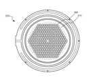
[0048]図3は、実施形態に係る処理チャンバと共に使用するためのシャワーヘッド325の底面図である。シャワーヘッド325は、図2Aに示すシャワーヘッド225に対応し得る。第1の流体チャネル219を図示する貫通穴365は、シャワーヘッド225を通る前駆体の流れを制御し、影響を与えるために、複数の形状及び構成を有し得る。第2の流体チャネル221を図示する小さな穴375は、貫通穴365の間でさえ、シャワーヘッドの表面全体に実質的に均一に分布され得、前駆体がシャワーヘッドを出るときに、他の構成よりも均一な前駆体の混合を提供するのに役立ち得る。3 is a bottom view of a
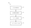
[0049]本技術の幾つかの実施形態に係るシャワーヘッドを製造するための方法400の例示的な工程を示す図4を参照する。上記のように、プラズマ生成電極又は接地電極のいずれかを含む、プラズマ工程中に電極として動作し得る幾つかのシャワーヘッド又はチャンバ構成要素は、セラミック又は誘電体材料で形成され得、誘電体と共に組み込まれる、又は誘電体内に組み込まれる導電性材料を含み得る。本開示全体に記載されるシャワーヘッドは、面板、イオンサプレッサ、ガス分配アセンブリ、又は上記チャンバで使用される他のシャワーヘッド又はマニホールド、又はプラズマ工程で上記構成要素を利用し得る他のいずれかのチャンバを含む、前述の構成要素のいずれかとして使用され得る。したがって、特定の設計を示したが、多くの異なる構成が本技術によって等しく包含されることを理解すべきである。[0049] Reference is now made to FIG. 4, which illustrates exemplary steps of a
[0050]幾つかの実施形態では、導電性材料は、形成工程中にシャワーヘッド内に組み込まれ得る、又はシャワーヘッド内に埋め込まれ得る。記載の構成要素の幾つかはセラミックであり得、構成要素は、熱及び/又は圧力を使用して構成要素を形成する成形工程で形成され得る。例えば、焼結を使用して、1又は複数の成形されたグリンボディからシャワーヘッドが形成され得る。シャワーヘッドを製造するための方法400の幾つかの実施形態では、工程405において、一体化して焼結し、例示的なシャワーヘッドを製造することができる2つのグリンボディ等のグリンボディが形成され得る。グリンボディは、円盤状であり得る、又は例示的な処理チャンバに着座するように他の任意の形状によって特徴付けられ得る。グリンボディは、焼成工程の前に2つの構成要素を結合することを可能にする1又は複数のプラグ穴又はスタッドを含むように成形され得、ボディは、幾つかのより大きいセットを含み得る、又はボディ間に分散された幾つかのスタッド及び/又はプラグ穴を含み得る。[0050] In some embodiments, the conductive material may be incorporated into the showerhead during the forming process or may be embedded in the showerhead. Some of the components described may be ceramic, and the components may be formed in a molding process that uses heat and/or pressure to form the components. For example, the showerhead may be formed from one or more molded green bodies using sintering. In some embodiments of the
[0051]グリンボディが形成されると、工程410において、導電性材料がグリンボディの1つに適用又は着座され得る。導電性材料は、以下に説明するように、特定の領域内のグリンボディの一方又は両方に適用されるメッシュ、フォイル、又はコーティングであり得る。導電性材料は、ガス流を提供するために後に穿孔されてシャワーヘッドになり得る開孔と同様のパターンであり得る開孔を含むように事前に形成され得る。例示的なシャワーヘッドは、数十、数百、又は数千の開孔を含み得、したがって、導電性材料の位置決めは、開孔形成により導電性材料が露出し得ないように実行され得る。上で説明したように、プラズマ放出物に暴露され得る導電性材料は、プラズマによってエッチングされ得る、スパッタされ得る、又はその他の方法で損傷を受ける可能性がある。したがって、例示的なシャワーヘッドの開発は、プラズマ曝露が起こり得る領域における導電性材料の曝露を明示的に制限するように実行され得る。[0051] Once the Grin bodies are formed, a conductive material may be applied or seated on one of the Grin bodies in
[0052]例えば、開孔は、完成したセラミックを通して形成又は穿孔され得る。したがって、導電性材料は、導電性材料を露出させることなくシャワーヘッド開孔を製造することを可能にする開孔を含むように、グリンボディに形成又は適用され得る。幾つかの実施形態では、導電性材料自体は、それがグリンボディ上に位置づけされるときに開孔を含み得る。例えば、画定される開孔を含むフォイルが製造され得る。追加の開孔は、後続の機械加工のためにフォイル開孔の位置決め機能を提供し得る、グリンボディのプラグ穴又はスタッドに対応し得る。別の例として、グリンボディが成形され得るために、プラグ穴及びスタッドが、開孔が製造され得る位置に対応するようにグリンボディ型の周りに分散され得、これにより、焼成工程中のずれが制限され得る。例えば、メッシュ又はフォイルがスタッドの周りのグリンボディに圧入され得る。メッシュタインをスタッドの周りで分離させることができ、これにより、型全体で導電性材料を一貫して適用することができ、鋭いエッジによる切断が制限され得る。[0052] For example, apertures can be formed or drilled through the finished ceramic. Thus, the conductive material can be formed or applied to the GRIN body to include apertures that allow for the production of showerhead apertures without exposing the conductive material. In some embodiments, the conductive material itself can include apertures when it is positioned on the GRIN body. For example, a foil can be produced that includes defined apertures. Additional apertures can correspond to plug holes or studs in the GRIN body that can provide a positioning function for the foil apertures for subsequent machining. As another example, plug holes and studs can be distributed around the GRIN body mold to correspond to the locations where the apertures can be produced so that the GRIN body can be molded, thereby limiting shifting during the firing process. For example, a mesh or foil can be pressed into the GRIN body around the studs. The mesh tines can be separated around the studs, which allows for consistent application of the conductive material throughout the mold and limits cutting by sharp edges.
[0053]導電性材料が適用されると、グリンボディが焼成されて、工程415においてシャワーヘッドが製造され得る。焼成は、セラミック構成要素を製造するための熱及び/又は圧力の印加を含み得る。上記焼成は、例えば、低温加熱とそれに続く高温加熱を含む複数の工程を含み得る。構成要素が形成された後、シャワーヘッドは、工程420においてパターニングされ得、これにより、機械加工中に開孔、チャネル、及び他の特徴が提供されて、最終的なシャワーヘッドが製造され得る。これらの製造されたシャワーヘッドは、シャワーヘッド全体に含まれる導電性材料を露出させ得ないシャワーヘッドの内部領域に幾つかの開孔を画定し得る。したがって、シャワーヘッドは、導電性材料がチャンバ処理領域内に露出されるのを制限又は防止しながら、流れ分配構成要素及び電極の両方として動作することができる。[0053] Once the conductive material is applied, the green body may be fired to produce the showerhead in
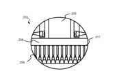
[0054]図5Aは、本技術の幾つかの実施形態に係る例示的なシャワーヘッド500を示す概略部分上面図である。シャワーヘッドは、例えばセラミックであり得る誘電体プレート505を含み得、シャワーヘッドはまた、組み込まれた導電性材料510を含み得る。図5Bは、本技術の幾つかの実施形態に係る例示的なシャワーヘッド500を示す概略部分断面図であり、図5Aと共にシャワーヘッドの様々な特徴を説明するものと見なすことができる。上記のように、シャワーヘッド500は、本技術によって包含される構成要素の1つの例示的な構成にすぎない。シャワーヘッド500は、本技術に係る様々なシャワーヘッドと共に含まれ得る機能を図示したものであるが、同様に包含される他の設計を制限するものではない。シャワーヘッド500は、前述のマニホールドのいずれかであり得、単一部品構成要素であり得る、又は幾つかの実施形態では、前述のようなガス分配アセンブリを製造するため等、構成要素の組み合わせの1つであり得る。シャワーヘッド500は、前述のような半導体処理チャンバ、又は本技術の実施形態における任意の他の処理チャンバ又はシステムに含まれ得る。5A is a schematic partial top view of an
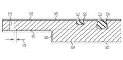
[0055]図示したように、誘電体プレート505は、上述した方法400によって、又は任意の他の方法によって形成されたセラミックプレートであり得、組み込まれた導電性材料510を含み得る。誘電体プレート505は、第1の面507と、第1の面507の反対側であり得る第2の面509とを含み得る。誘電体プレート505は、第1の面507から第2の面509まで延在する、プレートを通る幾つかの開孔515を画定し得、シャワーヘッドを通る前駆体のための経路を提供し得る。開孔515は、上記のように焼結した後、及び導電性材料510が組み込まれた後に、シャワーヘッドを通して形成され得る。幾つかの実施形態では、開孔515は、導電性材料510に接触又は導電性材料510を露出させ得ない。図示したように、導電性材料510は、開孔515の一部又はすべての周りに延在し得る。図5Bに示すように、導電性材料510は、形成されたときに開孔により導電性材料が露出されないようにするために、各開孔の周りに分離又は間隙518を維持し得る。[0055] As shown, the
[0056]誘電体プレート505は、1又は複数のチャネル、ならびに導電性材料510の組み込み後に機械加工され得る1又は複数の凹んだ特徴を画定し得る。焼結工程中に、材料特性と性質が変化し得、導電性材料、フォイル、又はメッシュが分散され得る。例えば、焼成する前に、誘電体プレート内の導電性材料510の正確な深さは既知であり得る。ただし、焼成後に、この位置がわずかに変化し得る。ラジアル間隙518により、開孔形成中にいずれの横方向の動きにも対応することができるようになる。しかしながら、導電性材料は、幾つかの実施形態では厚さがわずか数百ナノメートルであり得るため、任意の厚さが使用可能であるが、深さのわずかな変化により、電極結合及び特徴形成のための導電性材料の位置決めが困難になり得る。例えば、幾つかの例示的なシャワーヘッドは、第2の面509の内部領域に形成された凹部520を含み得る。焼成中に導電性材料510の位置がずれた場合、凹部520が形成されたときに導電性材料510が不注意に露出する可能性がある。本技術は、誘電体プレートでの導電性材料の露出を制限又は防止するために、幾つかの方法で位置決めを実行することができる。[0056] The
[0057]誘電体プレート505は、誘電体プレート505の第1の面507に第1の環状チャネル525を画定し得る。第1の環状チャネル525は、複数の開孔515の周りに延在し得、シャワーヘッドの内部領域526を画定し得る。第1の環状チャネル525は、真空工程中にシールを生成するために、Oリング又はエラストマー要素527を着座させるように構成され得る。したがって、内部領域526は、例えばプラズマ処理等の実行されている任意の処理にチャンバ内で暴露され得るシャワーヘッド500の一部であり得る。幾つかの実施形態では、導電性材料510は、開孔515が形成される場所を含めて、内部領域526のどこにも露出され得ない。[0057] The
[0058]導電性材料510は電極として結合され得るため、導電性材料は、結合を得るために少なくとも1つの位置で露出され得る。幾つかの実施形態では、誘電体プレート505は、誘電体プレート505の第1の面507に第2の環状チャネル530を画定し得る。第2の環状チャネル530は、RFガスケット533、又は導電性材料510に接触し得る任意の他の導電性接続を着座させるように構成され得る。第2の環状チャネル530は、第1の環状チャネル525から半径方向外側に形成され得、したがって、チャンバの処理領域の外部の位置に位置づけされ得る。したがって、第2の環状チャネル530は、例えば、チャンバ内で発生する事象に暴露され得ず、いかなるプラズマ放出物にも暴露され得ない。[0058] The
[0059]導電性材料510は、第2の環状チャネル530内の少なくとも1つの位置で露出され得、第2の環状チャネル530内の複数の位置で露出され得る。第2の環状チャネル530は、第1の環状チャネル525の半径方向外側に形成され得るので、導電性材料510は、第1の環状チャネル525を越えて延在し得る。第1の環状チャネル525での導電性材料の露出を防止するために、第2の環状チャネル530は、誘電体プレート505内で、第1の環状チャネル525よりも深い深さまで画定され得る。したがって、図5Bに示すように、導電性材料510は、第1の環状チャネル525より下の深さで第1の環状チャネル525を越えて延在し得、これにより、第1の環状チャネルでの導電性材料の露出が防止され得る。RFガスケット533が第2の環状チャネル530内に着座すると、ガスケットは、チャネル内に露出した導電性材料510に接触し得、これにより、導電性材料をチャンバ内の電極として動作させる経路が得られ得る。[0059] The
[0060]上記のように、導電性材料は、導電性材料の深さが既知のものとなるように、誘電体プレート内に位置づけされ得る。したがって、幾つかの実施形態では、第2の環状チャネル530は、シャワーヘッドの他の特徴の前に機械加工又は形成され得る。導電性材料510は、シャワーヘッドの外側領域まで完全に延在し得る、又は導電性材料510は、内部領域526のより均一なカバレッジから外部チャネル530が形成され得る外部領域まで延在する1又は複数のウイング又はタブ535を含み得る。1又は複数の位置決め穴又は溝を外部領域を通して下に形成して、例えば、含まれる場合に、タブ535の間等の導電性材料510の正確な深さが位置決めされ得る。既知になったら、第2の環状チャネル530を形成して、チャネル内の導電性材料510を完全に露出させることができる。導電性材料がシャワーヘッドの周りに延在し得、RFガスケット533又は他の電子結合もシャワーヘッドの周りに延在し得るため、位置決め中の外部領域の導電性材料の穿孔はいずれも、シャワーヘッドの周りに複数の接触点があることで、電極としての導電性材料の動作に影響を与えない可能性がある。[0060] As noted above, the conductive material can be positioned within the dielectric plate such that the depth of the conductive material is known. Thus, in some embodiments, the second
[0061]誘電体プレート505は、プラズマ種からの衝撃から保護し得る、ハロゲン含有プラズマ放出物等のプラズマ放出物に対して不活性であり得る任意の数の材料を含み得る。例えば、誘電体プレート505は、アルミニウム、イットリウム、ジルコニウム、シリコン、又は他の元素又は組み合わせを含む任意の数の金属の酸化物又は窒化物を含み得る。導電性材料は、電極として動作又は使用することができる任意の数の導電性材料であり得、アルミニウム、タングステン、モリブデン、タンタル、プラチナ、チタン、バナジウム、又はこれら又は他の導電性材料のいずれかの合金を含む任意の他の材料を含み得る。以下に記載される幾つかの実施形態は、焼結工程を含まない場合があるが、シャワーヘッドが方法400に従って製造され得る場合、焼成温度は1000℃をはるかに超える可能性がある。したがって、例えばアルミニウム等のより低い融点の金属は適切な候補でない場合がある。更に、セラミック材料及び導電性材料は、焼成中の膨張/収縮を制御するために、焼成温度に関する一定量のマッチングを生成するように選択され得る。[0061] The
[0062]製造されるシャワーヘッドの多孔度の量を制御するように、誘電体プレートを形成することもできる。構成要素は真空条件下で動作し得るため、真空状態又はシャワーヘッドによるガス抜きの影響を制限するために、多孔度が比較的低く維持され得る。同様に、より高い多孔度で特徴づけられる構成要素は、プラズマ種の吸収の増加の影響を受けやすい可能性があり、これにより、例えば、処理が実行される前に、より長いシーズニングを必要とし得る。したがって、幾つかの実施形態では、誘電体プレート505に使用される材料の多孔度は、約5%未満に制限され得、幾つかの実施形態では、約3%以下、約2%以下、約1%以下、約0.9%以下、約0.8%以下、約0.7%以下、約0.6%以下、約0.5%以下、約0.4%以下、約0.3%以下、約0.2%以下、又は約0.1%以下に制限され得る。[0062] The dielectric plate can also be formed to control the amount of porosity of the showerhead produced. Because the components may operate under vacuum conditions, the porosity can be kept relatively low to limit the effects of outgassing by the vacuum or showerhead. Similarly, components characterized with higher porosity may be susceptible to increased absorption of plasma species, which may require longer seasoning before processing can be performed, for example. Thus, in some embodiments, the porosity of the material used for the
[0063]多くの金属構成要素のように、コーティングの前に開孔が形成される場合、より小さい開孔が実現可能でない可能性がある、又は完全なコーティングが行われない場合がある。ただし、コーティングを容易にするために形成される開孔が大きいほど、プラズマ漏れが発生する可能性が高くなる。本技術は、開孔が導電性材料510に接触することなく誘電体プレート505を通ってのみ延在し得るため、これらの問題を克服する。したがって、コーティングの問題は、開孔の形成により導電性材料が露出し得ないセラミック材料を使用することによって克服されるため、後続のコーティングが実行され得る従来の材料よりも小さい開孔が穿孔され得る。したがって、幾つかの実施形態では、開孔515は、約10mm以下の直径によって特徴付けられ得、幾つかの実施形態では、約9mm以下、約8mm以下、約7mm以下、約6mm以下、約5mm以下、約4mm以下、約3mm以下、約2mm以下、約1mm以下の直径によって特徴付けられ得る。開孔サイズは、形成中に起こり得る移動量とともに、維持され得る間隙518に影響を及ぼし得る。したがって、半径方向の間隙であり得る間隙518は、各開孔の周りに約5mm以下延在し得、幾つかの実施形態では、各開孔の周りに約4mm以下、約3mm以下、約2mm以下、約1mm以下又は約0.5mm以下延在し得、これにより、開孔の形成中に導電性材料が露出されなくなる。[0063] As with many metal components, if the apertures are formed prior to coating, smaller apertures may not be feasible or complete coating may not occur. However, the larger the apertures formed to facilitate coating, the greater the chance of plasma leakage. The present technique overcomes these problems because the apertures may extend only through the
[0064]本技術に係るシャワーヘッドはまた、導電性材料の内部チャンバ環境への曝露を制限又は防止するための1又は複数のコーティングを含み得る。図6は、本技術の幾つかの実施形態に係る方法600の例示的な工程を示す図である。方法600は、前述のものと同様のシャワーヘッド、ならびに前述のような他のチャンバマニホールド又はディフューザを製造することができる。方法600は、誘電体構成要素を製造するための方法400の工程のいずれかを含み得、製造されたシャワーヘッドは、前述した材料、特性、又は性質のいずれかを含み得る。[0064] Showerheads according to the present technology may also include one or more coatings to limit or prevent exposure of conductive materials to the internal chamber environment. FIG. 6 illustrates exemplary steps of a
[0065]方法600は、方法400と同様に、本技術に係る方法の幾つかの実施形態に具体的に関連し得る又はし得ない1又は複数のオプションの工程を含み得る。例えば、工程の多くは、構造形成のより広い範囲を提供するために説明しているが、本技術にとって重要ではない、又は以下に更に説明する代替の方法論によって実行され得る。方法600は、方法600の工程と併せて説明する、図7A~図7Cの例示的なシャワーヘッド700の上面図に概略的に図示した工程を説明するものである。シャワーヘッド700は、同様に、本技術の実施形態における任意の処理チャンバに組み込まれ得る。図7は、例示の目的で一般的な概略図のみを図示したものであり、例示的なシャワーヘッドは、説明するように、任意の数の開孔又は構造要素を含み得ることを理解すべきである。[0065]
[0066]方法600は、工程605において開孔及び他の特徴を製造するためにプレートをエッチングすることを含み得る。例えば、上記のシャワーヘッド500の特徴、材料、又は性質のいずれかを有し得る開孔が、セラミック又は誘電体プレートを通して穿孔され得る。図7Aに示すように、開孔715は、シャワーヘッド700を製造するときに、誘電体プレート705を通して穿孔又は形成され得る。導電性又は金属材料のメッシュ、フォイル、印刷、又はスプレーが、工程610において、1又は複数の面上のプレートに適用され得る。導電性材料は、前述の導電性材料のいずれかであり得、シャワーヘッドの第1の面等の1又は複数の面上に位置づけ又は形成され得る。図7Bは、シャワーヘッド700の第1の面上での導電性材料710の形成を示すものである。図示したように、導電性材料710は、シャワーヘッドの第1の面全体に延在し得るが、間隙712は、各開孔の周りに維持され得る。例えば、導電性材料は、開孔から離れて、各開孔から第1の半径方向の距離に維持され得、これは、上記の任意の間隙距離に対応し得る。間隙712は、導電性材料が露出され得ないようにする同様の特徴を呈し得るが、間隙はまた、以下に説明するように、その後に追加されるコーティングのためのスペースも提供し得る。間隙は、事前に形成された導電性材料に含まれ得る、又は間隙を生じさせるために別のマスキング工程が実行され得る。[0066] The
[0067]次に、形成された開孔が、オプションの工程615でマスキングされ得る。マスキングは、穴の周りで実行され、各開孔の周りで半径方向又は横方向に限られた距離だけ延在し得る。次に、コーティングが工程620において塗布され、導電性材料710が覆われ得る。コーティングが塗布された後、マスクが、オプションの工程625で除去され得る。コーティングはまた、誘電体材料であり得、プレートの第1の誘電体材料に対する第2の誘電体材料であり得る。図7Cは、導電性材料710全体に延在するようにコーティング720が後に塗布されたシャワーヘッドを示す図である。コーティング720はまた、各開孔715からの間隙722を維持するために塗布され得、コーティング720は、各開孔からの第2の半径方向の距離に維持され得る。幾つかの実施形態では、第2の半径方向の距離は、第1の半径方向の距離よりも短くてよく、これにより、コーティング720が導電性材料710を完全に覆うようになり得る。[0067] The formed apertures may then be masked in
[0068]図7Cはまた、導電性材料710が、シャワーヘッド700の外部又は半径方向のエッジ725に沿った1又は複数の位置で露出され得ることを示している。露出は、エラストマー要素が着座し得る場所であり得る環状チャネル730の半径方向外側で発生し得る。環状チャネル730は、開孔の半径方向外側に画定され得、チャンバ内に露出され得るシャワーヘッドの内部領域と、チャンバ処理に露出され得ない外部領域との間の境界を画定し得る。図7Cに示したが、電極としての動作を可能にする材料の連続性を確保するために、開孔形成中にチャネルが前もって形成されていてよいことを理解されたい。したがって、導電性材料が領域725で露出されている場合、チャンバ環境内での導電性材料の露出を制限又は防止しながら、電極動作のための結合を可能にし得る。幾つかの実施形態では、ハイブリッドコーティングが塗布され得、シャワーヘッド全体に塗布される第1のコーティングを含み得るが、以下に記載されるような第2の層等の第2のより厚いコーティングは、エッジ領域に塗布され得ない。より薄いコーティングは、一部のプラズマ放出物から保護するが、電気的接触から完全に絶縁され得ない厚さのために、コーティングを介した電気的接続を可能にし得る。このオプションにより、幾つかの実施形態では、製造中に更なる柔軟性が得られ得る。[0068] FIG. 7C also illustrates that the
[0069]図7Dは、本技術の幾つかの実施形態に係る例示的なシャワーヘッドを示す概略部分断面図であり、例えば、シャワーヘッド700の別の図を示し得る。この図は、誘電体プレート705、導電性材料710、及びコーティング720を含むシャワーヘッドの一部を示しており、それらは、開孔715の周りに形成され得る。面取りされたエッジを有する開孔715を示したが、この図は、任意の開孔設計が本技術のいずれかに適応可能であることを単に例示するものであり、シャワーヘッド500、700、又は製造された他の任意のシャワーヘッドは、任意の開孔プロファイルによって特徴付けられ得る。7D is a schematic partial cross-sectional view showing an exemplary showerhead according to some embodiments of the present technology, which may show, for example, another view of
[0070]図7Dは、導電性材料710がプレート705の第1の面707全体にどのように形成され得るかを示す図である。幾つかの実施形態では、第2の面も1又は複数の材料を含み得るが、第1の面の反対側の第2の面709は、導電性材料又はコーティング720を含まなくてもよい。例えば、シャワーヘッド又はチャンバ構成要素の向きに応じて、構成要素の一方の側がより多くの衝撃に暴露され得、一方の側は化学反応性プラズマ放出物により多く暴露され得、コーティングはそれに応じて塗布され得るが、コーティングは、シャワーヘッドの片側又は両側に塗布可能である。図示したように、導電性材料710は、開孔715から第1の距離又は間隙712まで離れて維持され得る。コーティング720が、導電性材料710上に塗布され得、第1の間隙よりも短くてよい第2の距離又は間隙722に塗布され得る。したがって、本技術の実施形態では、導電性材料710は、シャワーヘッドの内部領域で完全に覆われ得る。7D illustrates how a
[0071]プレート及びコーティングの両方の誘電体材料は、前述の材料のいずれかであり得、導電性材料はまた、前述の材料のいずれかであり得る。さらに、コーティング720は、幾つかの実施形態では、一種のハイブリッド又は多層コーティングであり得る。例えば、コーティング720の第1の層が、導電性材料の第2のコーティング層への露出を制限するために含まれ得、これにより、例えば、導電性材料に対する酸化又は他の影響が制限され得る。[0071] The dielectric material of both the plate and the coating can be any of the materials previously described, and the conductive material can also be any of the materials previously described. Additionally, coating 720 can be a type of hybrid or multi-layer coating in some embodiments. For example, a first layer of
[0072]本技術の幾つかの実施形態に係るチャンバは、バイアスプラズマが基板処理領域に形成され得る修飾工程を実行するために使用され得る。この工程は、基板上の構造の物理的衝撃であってよく、不活性又は反応性の低い前駆体を用い得る。さらに、反応性エッチングが、遠隔領域に反応性プラズマ放出物を生成することによって実行され得る。前駆体は、基板から修飾された材料を除去するように構成され得るハロゲン前駆体を含み得る。したがって、記載されたシャワーヘッド等のチャンバの構成要素は、フッ素、塩素、又は他のハロゲン含有放出物等の化学反応性プラズマ放出物、ならびに物理的修飾に使用されるバイアスプラズマで生成されるイオンの両方に暴露され得る。例えば、例示的なシャワーヘッドは、基板に面する面及び開孔内に接触するバイアスプラズマ放出物等のプラズマ放出物、ならびに基板と相互作用する前に開孔を通って進む反応性放出物の両方に曝露され得る。上記の他の構成要素もまた、逆流するプラズマ放出物からのものを含む、一方又は両方のプラズマ放出物に曝露され得る。従来の構成要素は、プラズマ材料への導電性構成要素の曝露により劣化し得るが、本技術のシャワーヘッドは、プラズマ電極として動作しながら、導電性材料のいかなる曝露も制限又は防止し得る。[0072] The chamber according to some embodiments of the present technology may be used to perform a modification process in which a biased plasma may be formed in the substrate processing region. This process may be a physical bombardment of structures on the substrate and may use inert or less reactive precursors. Additionally, reactive etching may be performed by generating reactive plasma effluents in a remote region. The precursors may include halogen precursors that may be configured to remove modified materials from the substrate. Thus, components of the chamber, such as the described showerhead, may be exposed to both chemically reactive plasma effluents, such as fluorine, chlorine, or other halogen-containing effluents, as well as ions generated in the biased plasma used for physical modification. For example, the exemplary showerhead may be exposed to both plasma effluents, such as biased plasma effluents that contact the surface facing the substrate and within the apertures, as well as reactive effluents that travel through the apertures before interacting with the substrate. Other components listed above may also be exposed to one or both plasma effluents, including those from backflowing plasma effluents. While conventional components may be degraded by exposure of conductive components to plasma materials, the showerhead of the present technology may limit or prevent any exposure of conductive materials while operating as a plasma electrode.
[0073]プラズマ放出物は、チャンバ構成要素に異なる効果をもたらす可能性がある。例えば、イオンは、シャワーヘッドによって、遠隔で生成された化学反応性プラズマ放出物から少なくとも部分的に濾過され得る。しかしながら、例えば、フッ素含有放出物等の反応性放出物は、従来の構成要素設計でフッ化アルミニウムを形成すること等によって、露出した材料の腐食を引き起こす可能性がある。経時的に、このプロセスは露出した金属構成要素を腐食させ、交換が必要になる場合がある。さらに、基板処理領域でバイアスプラズマから形成されたプラズマ種は、構成要素に影響を与え、物理的損傷やスパッタリングを引き起こし、経時的に構成要素を侵食し得る。したがって、記載の構成要素のいずれも、チャンバの1又は複数の領域内で生成されたプラズマ放出物からの化学的腐食ならびに物理的侵食の影響を受けやすい可能性がある。[0073] Plasma effluents can have different effects on chamber components. For example, ions can be at least partially filtered from remotely generated chemically reactive plasma effluents by the showerhead. However, reactive effluents, such as fluorine-containing effluents, can cause corrosion of exposed materials, such as by forming aluminum fluorides in conventional component designs. Over time, this process can corrode exposed metal components and require replacement. Additionally, plasma species formed from the bias plasma in the substrate processing region can impact components, causing physical damage and sputtering, eroding the components over time. Thus, any of the described components can be susceptible to chemical corrosion as well as physical erosion from plasma effluents generated in one or more regions of the chamber.
[0074]腐食は、材料上にコーティング720を形成することによって、又はコーティングのために特定の材料を使用することによって、幾つかの方法で制御することができる。例えば、アルミニウムはフッ素含有プラズマ放出物への暴露によって腐食し得るが、酸化アルミニウム、又は他のめっき又はコーティングは、プラズマ放出物との接触で腐食しない可能性がある。したがって、記載の構成要素のいずれも、陽極酸化、酸化、原子層堆積、化学気相堆積、プラズマ溶射、無電解ニッケルめっき、電気めっきニッケル、チタン酸バリウム、又は露出した導電性材料を化学腐食から保護し得る他の任意の材料、例えばアルミニウム、モリブデン、プラチナ、又は前述の材料のいずれか等によってコーティングされ得る又は保護され得る。同様に、侵食は、材料上にコーティングを形成することによって、又はベースプレート705に特定の材料を使用することによって、幾つかの方法で制御することができる。例えば、アルミニウムやジルコニウムを含む追加の材料を含む場合と含まない場合とがある酸化イットリウム等の高性能材料は、バイアスプラズマ放出物によって引き起こされる物理的損傷から構成要素を保護し得る。ただし、構造に腐食性プラズマ放出物と侵食性プラズマ放出物の両方が接触し得る場合は、構成要素への損傷が依然として発生し得る。したがって、コーティング720は、記載のように複数の材料を含み得、ベースプレート705は、追加のコーティングも含み得る。材料は、実施形態において同じであり得る、異なり得る、又は組み合わせであり得る。例えば、コーティング720は、幾つかの実施形態では、プラズマ放出物に対する耐性を増強することが指摘されている他のいずれかの材料とともに、プラズマ溶射酸化イットリウムを含み得る。[0074] Corrosion can be controlled in several ways by forming a
[0075]さらに、ハイブリッドコーティング720の第1の層は、導電性材料710全体に共形的に延在し得る。前に説明したように、第1の層は、ハロゲン含有放出物又はエッチャント材料を含む反応性エッチャントから導電性材料を保護するように構成された耐食層であり得る。第1の層は、実施形態では、陽極酸化、無電解ニッケルめっき、電気めっきニッケル、酸化アルミニウム、又はチタン酸バリウムであり得る、又はそれらを含み得る。耐食性コーティングの形成プロセスにより、導電性材料の完全なカバレッジが達成され得る。カバレッジの深さは、約25μm以下であり得、約20μm以下、約15μm以下、約10μm以下、約5μm以下、約3μm以下、約1μm以下、約750nm以下、約500nm以下、約250nm以下、約100nm以下、又は約50nm以下であり得る。幾つかの実施形態では、厚さの増加を達成するための時間が比較的長くなり得るため、コーティングの厚さは、幾つかの実施形態では、約100nmから約300nmの間であり得る。第1の層の厚さが約3μm又は約5μm以上であり得る実施形態では、第2の層は含まれなくてよい。[0075] Additionally, the first layer of the
[0076]ハイブリッドコーティングの第2の層もまた、第1の層の外部に含まれ得る。第2の層は、酸化イットリウム、又は電子ビームコーティング又はアルミニウム、ジルコニウム、又は他の材料を含む酸化イットリウム等の他の高性能材料を含み得る。第2の層は、第1の面707全体で少なくとも部分的に延在していてよく、構成要素のプラズマに面する面全体に延在し得る。ハイブリッドコーティングの第2の層は、約25μm以下の厚さによって特徴付けられ得、幾つかの実施形態では、約20μm以下、約15μm以下、約10μm以下、約5μm以下、約1μm以下、約750nm以下、約500nm以下、約300nm以下、又は約100nm以下の厚さによって特徴付けられ得る。[0076] A second layer of hybrid coating may also be included external to the first layer. The second layer may include yttrium oxide or other high performance materials such as electron beam coating or yttrium oxide with aluminum, zirconium, or other materials. The second layer may extend at least partially across the
[0077]前述したように、コーティング720を塗布する前にマスキング工程が実行され得る。コーティングは、幾つかの実施形態ではスプレー機構によって塗布され得るので、前述のようなサイズであり得る開孔を通しての送達は困難であり得る。マスキングを行わないと、コーティングの完全な層が形成され得ず、一貫性のないコーティングから形成されたピッチングが発生する可能性があり、これにより、経時的な処理中にコーティングが除去されやすくなり、塗布の再現性が制限され得る。したがって、マスキングは、これが問題となる可能性があり且つコーティングを導電性材料及びプレートの第1の面に明確に沿うように限定し得る幾つかの実施形態で実行され得る。[0077] As previously mentioned, a masking step may be performed prior to application of
[0078]プレート705及び/又は導電性材料710は、幾つかの実施形態では、2つの層が使用される場合に、コーティングの第1の層又は第2の層の一方又は両方を形成する前に、テクスチャ加工され得る。例えば、コーティングは、テクスチャ加工された面への接着性が改善されていてよい。幾つかの実施形態では、テクスチャ加工は、ハイブリッドコーティングの一方又は両方の層の深さまで、又はそれよりも深い深さまで実行され得る。例えば、第1の層をコーティングする前に、又は第1の層と第2の層のコーティングとの間に、プレート及び/又は導電性材料が、機械加工、ビード又は他のブラスト技法、又は他の粗面化又はテクスチャ加工工程を介してテクスチャ加工され得る。テクスチャ加工は、少なくとも約50nmの深さまで実行され得、少なくとも約100nm、少なくとも約250nm、少なくとも約500nm、少なくとも約750nm、少なくとも約1μm、少なくとも約3μm、少なくとも約5μm、又はそれ以上の深さまで実行され得るが、テクスチャ加工は、下にある材料の露出を制限し、カバレッジを確保するために、材料の全体の厚さよりも深い深さまで拡張することはできない。[0078] The
[0079]図8は、本技術の幾つかの実施形態に係る方法800の例示的な工程を示す図である。方法800は、方法600で上述したシャワーヘッド形成の変形を含み得る。本方法を、本技術の幾つかの実施形態に係る例示的なシャワーヘッド900を示す概略上面図である図9A~図9Bを参照しながら説明する。方法800は、方法800でのコーティングに続いて開孔が形成され得るという点で、方法600とは異なり得る。例えば、方法800は、続いて開孔が穿孔され得る誘電体プレート上にマスクを形成することによって工程805において開始され得る。マスキングの後に、導電性メッシュ、フォイル、又はコーティングが、金属印刷又は金属堆積を含む幾つかの前述の技法によって実行され得、前述のように行われ得、続いて開孔が形成される間隙距離が維持され得る工程810において、適用され得る。工程815において、前述のように、第2の間隙を維持し得るコーティングが導電性材料上に塗布され得る。8 is a diagram illustrating exemplary steps of a
[0080]図9Aは、工程815でのコーティングに続く例示的なシャワーヘッドを示し得る。図示したように、シャワーヘッド900は、プレート905を通して開孔が形成されない場合があるが、図7で説明したシャワーヘッドに類似していてよい。マスク材料は、工程820において除去され得、次いで、開孔が、工程825においてプレートを通して機械加工され得る。図9Bに示すように、最終的なシャワーヘッドは、開孔915がコーティングに続いて形成されたが、図7の最終的シャワーヘッドに類似し得る。[0080] FIG. 9A may show an exemplary showerhead following coating at
[0081]本技術の実施形態に係るシャワーヘッドは、導電性ベース材料に基づいていてよい従来のシャワーヘッドよりも改善された耐食性及び耐侵食性を提供し得る。記載したように、導電性材料をセラミック又は他の誘電体材料と共に又はその中に組み込むことにより、処理チャンバ内の導電性材料の開孔サイズの縮小及び完全なカバレッジを含む改善されたカバレッジを可能にしつつ、電極としての動作も可能である。[0081] Showerheads according to embodiments of the present technology may provide improved corrosion and erosion resistance over conventional showerheads that may be based on conductive base materials. As described, incorporating a conductive material with or within a ceramic or other dielectric material allows for reduced aperture size and improved coverage, including complete coverage, of the conductive material within the processing chamber while also allowing operation as an electrode.
[0082]前述において、説明の目的で、本技術の様々な実施形態の理解を提供するために、多くの詳細を提示している。しかしながら、特定の実施形態は、これらの詳細の一部なしで、又は追加の詳細とともに実施され得ることが当業者には明らかであろう。[0082] In the foregoing, for purposes of explanation, numerous details are presented in order to provide an understanding of various embodiments of the present technology. However, it will be apparent to one of ordinary skill in the art that certain embodiments may be practiced without some of these details or with additional details.
[0083]幾つかの実施形態を開示したが、実施形態の主旨から逸脱することなく、様々な修正、代替構造、及び同等物を使用できることが当業者によって認識されるであろう。さらに、本技術を不必要に曖昧にすることを避けるために、幾つかの周知のプロセス及び要素は説明していない。したがって、上記の説明を、本技術の範囲を限定するものと解釈すべきではない。さらに、方法又はプロセスは、順次又は段階的に説明され得るが、工程は、同時に、又は列挙されたものとは異なる順序で実行され得ることが理解されるべきである。[0083] Although several embodiments have been disclosed, those skilled in the art will recognize that various modifications, alternative structures, and equivalents may be used without departing from the spirit of the embodiments. Moreover, some well-known processes and elements have not been described to avoid unnecessarily obscuring the present technology. Thus, the above description should not be construed as limiting the scope of the present technology. Furthermore, although a method or process may be described sequentially or stepwise, it should be understood that the steps may be performed simultaneously or in a different order than that listed.
[0084]値の範囲が提供される場合、文脈が明確に別段の指示をしない限り、その範囲の上限と下限との間の、下限の単位の最小部分までの各介在値もまた、具体的に開示されることを理解されたい。いずれかの記載された値又は記載された範囲の記載されていない介在値と、その記載された範囲の他のいずれかの記載された値又は介在値との間のいかなるより狭い範囲も含まれる。これらのより小さい範囲の上限と下限は、独立して範囲に含まれる又は除外される場合があり、より小さい範囲に一方、又は両方の限界値が含まれる、又はどちらも含まれない各範囲も、記載された範囲におけるいずれかの特に除外された限界値に従って、本技術に含まれる。記載された範囲に限界値の一方又は両方が含まれる場合、それら含まれる限界値の一方又は両方を除外する範囲も含まれる。[0084] Where a range of values is provided, it is understood that each intervening value between the upper and lower limits of that range, to the smallest fraction of the unit of the lower limit, is also specifically disclosed, unless the context clearly dictates otherwise. Any narrower range between any stated value or unstated intervening value in a stated range and any other stated or intervening value in that stated range is included. The upper and lower limits of these smaller ranges may be independently included or excluded in the range, and each range in which either or both limits are included in the smaller range is also included in the technology, subject to any specifically excluded limits in the stated range. When one or both limits are included in a stated range, ranges excluding one or both of those included limits are also included.
[0085]本明細書及び添付の特許請求の範囲で使用される場合、単数形「a」、「an」、及び「the」は、文脈が明確に別段の指示をしない限り、複数形の参照を含む。したがって、例えば、「1つの前駆体(a precursor)」への言及は、複数の上記前駆体を含み、「層(the layer)」への言及は、当業者に周知の1又は複数の層及びその同等物への言及等を含む。[0085] As used herein and in the appended claims, the singular forms "a," "an," and "the" include plural references unless the context clearly dictates otherwise. Thus, for example, a reference to "a precursor" includes a plurality of such precursors, a reference to "the layer" includes a reference to one or more layers and equivalents thereof known to those skilled in the art, and so forth.
[0086]また、本明細書及び以下の特許請求の範囲で使用する場合、「含む、備える(comprise)」、「含む、備える(comprising)」、「含む(contain)」、「含む(containing)」、「含む(include)」、及び「含む(including)」という用語は、記載された特徴、整数、構成要素、又は工程の存在を指定するものであるが、1又は複数の他の特徴、整数、構成要素、工程、実施、又は群の存在又は追加を排除するものではない。[0086] Additionally, as used herein and in the claims that follow, the terms "comprise," "comprising," "containing," "containing," "including," and "including" specify the presence of stated features, integers, components, or steps, but do not exclude the presence or addition of one or more other features, integers, components, steps, operations, or groups.
Claims (20)
Translated fromJapanese誘電体プレートの複数の開孔の位置のそれぞれから第1の径方向距離に導電性材料が維持された状態で、前記誘電体プレートの第1の面に前記導電性材料を適用することと、
前記複数の開孔の位置のそれぞれから第2の径方向距離にある前記複数の開孔の位置をマスキングすることと、
前記複数の開孔の位置をマスキングした後、前記導電性材料の露出部分に誘電体コーティングを適用することと、
を含む方法。 1. A method of manufacturing a showerhead for a semiconductor processing system, comprising:
applying a conductive material to a first surface of the dielectric plate while maintaining the conductive material a first radial distance from each of a plurality of aperture locations in the dielectric plate;
masking the plurality of aperture locations a second radial distance from each of the plurality of aperture locations;
applying a dielectric coating to exposed portions of the conductive material after masking locations of the plurality of apertures;
The method includes:
をさらに含む、請求項1に記載の、半導体処理システムのためのシャワーヘッドを製造する方法。 forming a plurality of apertures through a thickness of the dielectric plate, each aperture of the plurality of apertures disposed at one of the plurality of aperture locations;
10. The method of manufacturing a showerhead for a semiconductor processing system of claim 1, further comprising:
請求項2に記載の、半導体処理システムのためのシャワーヘッドを製造する方法。 forming the plurality of apertures includes one or both of drilling the plurality of apertures and etching the plurality of apertures.
3. The method of manufacturing a showerhead for a semiconductor processing system of claim 2.
請求項2に記載の、半導体処理システムのためのシャワーヘッドを製造する方法。 the plurality of apertures are formed prior to masking the locations of the plurality of apertures.
3. The method of manufacturing a showerhead for a semiconductor processing system of claim 2.
請求項2に記載の、半導体処理システムのためのシャワーヘッドを製造する方法。 the plurality of apertures are formed after applying the dielectric coating.
3. The method of manufacturing a showerhead for a semiconductor processing system of claim 2.
をさらに含む、請求項5に記載の、半導体処理システムのためのシャワーヘッドを製造する方法。 removing the masking layer prior to forming the plurality of apertures;
6. The method of manufacturing a showerhead for a semiconductor processing system of claim 5, further comprising:
をさらに含む、請求項1に記載の、半導体処理システムのためのシャワーヘッドを製造する方法。 removing said masking mask after applying said dielectric coating;
10. The method of manufacturing a showerhead for a semiconductor processing system of claim 1, further comprising:
前記導電性材料の前記露出部分に適用される第1の層と、
第2の層であって、前記第2の層を除く前記導電性材料の前記露出部分のエッジ領域をそのままにして、前記露出面の中央部分に適用される第2の層と、
を含む、請求項1に記載の、半導体処理システムのためのシャワーヘッドを製造する方法。 The dielectric coating comprises:
a first layer applied to the exposed portion of the conductive material;
a second layer applied to a central portion of the exposed surface, leaving an edge area of the exposed portion of the conductive material excluding the second layer;
10. The method of manufacturing a showerhead for a semiconductor processing system of claim 1, comprising:
1又は複数のグリンボディに前記導電性材料を適用することと、
前記第1の面に適用された前記導電性材料を有する前記誘電体プレートを形成するために、前記1又は複数のグリンボディ及び前記導電性材料を焼成することと、
を含む、
請求項1に記載の、半導体処理システムのためのシャワーヘッドを製造する方法。 Applying the conductive material comprises:
applying said conductive material to one or more green bodies;
firing the one or more GRIN bodies and the conductive material to form the dielectric plate having the conductive material applied to the first surface;
including,
10. The method of manufacturing a showerhead for a semiconductor processing system of claim 1.
をさらに含む、請求項1に記載の、半導体処理システムのためのシャワーヘッドを製造する方法。 10. The method of manufacturing a showerhead for a semiconductor processing system of claim 1, further comprising texturing one or both of the dielectric plate and the conductive material prior to applying at least a portion of the dielectric coating.
前記導電性材料の前記露出部分に適用される第1の層と、
第2の層であって、前記第2の層を除く前記導電性材料の前記露出部分のエッジ領域をそのままにして、前記露出面の中央部分に適用される第2の層と、
前記第1の層及び前記第2の層のいずれか又は両方まで又はより大きな深さに適用される前記テクスチャ加工のテクスチャと、
を含む、請求項16に記載の、半導体処理システムのためのシャワーヘッドを製造する方法。 The dielectric coating comprises:
a first layer applied to the exposed portion of the conductive material;
a second layer applied to a central portion of the exposed surface, leaving an edge area of the exposed portion of the conductive material excluding the second layer;
the texture of the texturing being applied to a depth up to or greater than either or both of the first layer and the second layer;
20. The method of manufacturing a showerhead for a semiconductor processing system of claim 16, comprising:
Applications Claiming Priority (5)
| Application Number | Priority Date | Filing Date | Title |
|---|---|---|---|
| US16/245,698 | 2019-01-11 | ||
| US16/245,698US10920319B2 (en) | 2019-01-11 | 2019-01-11 | Ceramic showerheads with conductive electrodes |
| JP2021539581AJP7237162B2 (en) | 2019-01-11 | 2019-12-06 | Ceramic shower head with conductive electrodes |
| PCT/US2019/064834WO2020146069A1 (en) | 2019-01-11 | 2019-12-06 | Ceramic showerheads with conductive electrodes |
| JP2023030072AJP7464772B2 (en) | 2019-01-11 | 2023-02-28 | Ceramic showerhead with conductive electrodes |
Related Parent Applications (1)
| Application Number | Title | Priority Date | Filing Date |
|---|---|---|---|
| JP2023030072ADivisionJP7464772B2 (en) | 2019-01-11 | 2023-02-28 | Ceramic showerhead with conductive electrodes |
Publications (2)
| Publication Number | Publication Date |
|---|---|
| JP7525752B1true JP7525752B1 (en) | 2024-07-30 |
| JP2024106347A JP2024106347A (en) | 2024-08-07 |
Family
ID=71516044
Family Applications (3)
| Application Number | Title | Priority Date | Filing Date |
|---|---|---|---|
| JP2021539581AActiveJP7237162B2 (en) | 2019-01-11 | 2019-12-06 | Ceramic shower head with conductive electrodes |
| JP2023030072AActiveJP7464772B2 (en) | 2019-01-11 | 2023-02-28 | Ceramic showerhead with conductive electrodes |
| JP2024054295AActiveJP7525752B1 (en) | 2019-01-11 | 2024-03-28 | Ceramic showerhead with conductive electrodes |
Family Applications Before (2)
| Application Number | Title | Priority Date | Filing Date |
|---|---|---|---|
| JP2021539581AActiveJP7237162B2 (en) | 2019-01-11 | 2019-12-06 | Ceramic shower head with conductive electrodes |
| JP2023030072AActiveJP7464772B2 (en) | 2019-01-11 | 2023-02-28 | Ceramic showerhead with conductive electrodes |
Country Status (6)
| Country | Link |
|---|---|
| US (3) | US10920319B2 (en) |
| JP (3) | JP7237162B2 (en) |
| KR (2) | KR102595824B1 (en) |
| CN (2) | CN119864270A (en) |
| TW (1) | TWI776107B (en) |
| WO (1) | WO2020146069A1 (en) |
Families Citing this family (10)
| Publication number | Priority date | Publication date | Assignee | Title |
|---|---|---|---|---|
| US11094508B2 (en)* | 2018-12-14 | 2021-08-17 | Applied Materials, Inc. | Film stress control for plasma enhanced chemical vapor deposition |
| US10920319B2 (en) | 2019-01-11 | 2021-02-16 | Applied Materials, Inc. | Ceramic showerheads with conductive electrodes |
| US20220028710A1 (en)* | 2020-07-21 | 2022-01-27 | Applied Materials, Inc. | Distribution components for semiconductor processing systems |
| JP7682377B2 (en)* | 2021-08-25 | 2025-05-23 | アプライド マテリアルズ インコーポレイテッド | Clamp-on dual channel shower head |
| CN118119733A (en)* | 2021-10-19 | 2024-05-31 | 应用材料公司 | Dummy holes and mesh patches for diffusers |
| JP7587056B2 (en)* | 2022-05-23 | 2024-11-19 | 株式会社日立ハイテク | How to recycle interior wall materials |
| US20240124978A1 (en)* | 2022-10-13 | 2024-04-18 | Eugenus, Inc. | Gas diffuser plate coated with emissivity-controlling thin film and methods of forming same |
| KR102761937B1 (en)* | 2022-11-24 | 2025-02-06 | (주)보부하이테크 | Method for manufacturing faceplate and method for manufacturing showerhead |
| KR20250072172A (en)* | 2023-11-16 | 2025-05-23 | (주)포인트엔지니어링 | Diffuser, Manufacturing Method thereof And PECVD |
| US20250259819A1 (en)* | 2024-02-08 | 2025-08-14 | Tokyo Electron Limited | Apparatus for plasma processing |
Citations (5)
| Publication number | Priority date | Publication date | Assignee | Title |
|---|---|---|---|---|
| JP2006210929A (en) | 2005-01-28 | 2006-08-10 | Applied Materials Inc | Plasma reactor overhead source power electrode with low arc discharge, cylindrical gas outlet and forming surface |
| JP2014509783A (en) | 2011-03-04 | 2014-04-21 | ノべラス・システムズ・インコーポレーテッド | Hybrid ceramic shower head |
| JP2014531753A (en) | 2011-09-07 | 2014-11-27 | ラム リサーチ コーポレーションLam Research Corporation | Dual chamber pulse plasma chamber |
| JP2016528380A (en) | 2013-06-20 | 2016-09-15 | アプライド マテリアルズ インコーポレイテッドApplied Materials,Incorporated | Plasma corrosion resistant rare earth oxide thin film coating |
| JP2016188424A (en) | 2015-01-12 | 2016-11-04 | ラム リサーチ コーポレーションLam Research Corporation | Gas distribution ceramic plate with embedded electrode |
Family Cites Families (2002)
| Publication number | Priority date | Publication date | Assignee | Title |
|---|---|---|---|---|
| US2369620A (en) | 1941-03-07 | 1945-02-13 | Battelle Development Corp | Method of coating cupreous metal with tin |
| US3451840A (en) | 1965-10-06 | 1969-06-24 | Us Air Force | Wire coated with boron nitride and boron |
| US3401302A (en) | 1965-11-01 | 1968-09-10 | Humphreys Corp | Induction plasma generator including cooling means, gas flow means, and operating means therefor |
| US3537474A (en) | 1968-02-19 | 1970-11-03 | Varian Associates | Push button vacuum control valve and vacuum system using same |
| US3756511A (en) | 1971-02-02 | 1973-09-04 | Kogyo Kaihatsu Kenyusho | Nozzle and torch for plasma jet |
| US3969077A (en) | 1971-12-16 | 1976-07-13 | Varian Associates | Alkali metal leak detection method and apparatus |
| US4232060A (en) | 1979-01-22 | 1980-11-04 | Richardson Chemical Company | Method of preparing substrate surface for electroless plating and products produced thereby |
| US4632857A (en) | 1974-05-24 | 1986-12-30 | Richardson Chemical Company | Electrolessly plated product having a polymetallic catalytic film underlayer |
| US4397812A (en) | 1974-05-24 | 1983-08-09 | Richardson Chemical Company | Electroless nickel polyalloys |
| US4006047A (en) | 1974-07-22 | 1977-02-01 | Amp Incorporated | Catalysts for electroless deposition of metals on comparatively low-temperature polyolefin and polyester substrates |
| US3937857A (en) | 1974-07-22 | 1976-02-10 | Amp Incorporated | Catalyst for electroless deposition of metals |
| US4341592A (en) | 1975-08-04 | 1982-07-27 | Texas Instruments Incorporated | Method for removing photoresist layer from substrate by ozone treatment |
| US4190488A (en) | 1978-08-21 | 1980-02-26 | International Business Machines Corporation | Etching method using noble gas halides |
| US4265943A (en) | 1978-11-27 | 1981-05-05 | Macdermid Incorporated | Method and composition for continuous electroless copper deposition using a hypophosphite reducing agent in the presence of cobalt or nickel ions |
| US4234628A (en) | 1978-11-28 | 1980-11-18 | The Harshaw Chemical Company | Two-step preplate system for polymeric surfaces |
| US4214946A (en) | 1979-02-21 | 1980-07-29 | International Business Machines Corporation | Selective reactive ion etching of polysilicon against SiO2 utilizing SF6 -Cl2 -inert gas etchant |
| US4361441A (en) | 1979-04-17 | 1982-11-30 | Plasma Holdings N.V. | Treatment of matter in low temperature plasmas |
| US4209357A (en) | 1979-05-18 | 1980-06-24 | Tegal Corporation | Plasma reactor apparatus |
| IT1130955B (en) | 1980-03-11 | 1986-06-18 | Oronzio De Nora Impianti | PROCEDURE FOR THE FORMATION OF ELECTROCES ON THE SURFACES OF SEMI-PERMEABLE MEMBRANES AND ELECTRODE-MEMBRANE SYSTEMS SO PRODUCED |
| US4361418A (en) | 1980-05-06 | 1982-11-30 | Risdon Corporation | High vacuum processing system having improved recycle draw-down capability under high humidity ambient atmospheric conditions |
| NL8004005A (en) | 1980-07-11 | 1982-02-01 | Philips Nv | METHOD FOR MANUFACTURING A SEMICONDUCTOR DEVICE |
| US4340462A (en) | 1981-02-13 | 1982-07-20 | Lam Research Corporation | Adjustable electrode plasma processing chamber |
| US4368223A (en) | 1981-06-01 | 1983-01-11 | Asahi Glass Company, Ltd. | Process for preparing nickel layer |
| DE3205345A1 (en) | 1982-02-15 | 1983-09-01 | Philips Patentverwaltung Gmbh, 2000 Hamburg | "METHOD FOR THE PRODUCTION OF FLUOREDOTED LIGHT-CONDUCTING FIBERS" |
| US4585920A (en) | 1982-05-21 | 1986-04-29 | Tegal Corporation | Plasma reactor removable insert |
| JPS591671A (en) | 1982-05-28 | 1984-01-07 | Fujitsu Ltd | Plasma cvd device |
| JPS59126778A (en) | 1983-01-11 | 1984-07-21 | Tokyo Denshi Kagaku Kabushiki | Method and device for plasma etching |
| JPS59222922A (en) | 1983-06-01 | 1984-12-14 | Nippon Telegr & Teleph Corp <Ntt> | Vapor growth apparatus |
| JPS6060060A (en) | 1983-09-12 | 1985-04-06 | 株式会社日立製作所 | Switchgear for door of railway rolling stock |
| US4579618A (en) | 1984-01-06 | 1986-04-01 | Tegal Corporation | Plasma reactor apparatus |
| US4656052A (en) | 1984-02-13 | 1987-04-07 | Kyocera Corporation | Process for production of high-hardness boron nitride film |
| US4656076A (en) | 1985-04-26 | 1987-04-07 | Triquint Semiconductors, Inc. | Self-aligned recessed gate process |
| US4600464A (en) | 1985-05-01 | 1986-07-15 | International Business Machines Corporation | Plasma etching reactor with reduced plasma potential |
| US4807016A (en) | 1985-07-15 | 1989-02-21 | Texas Instruments Incorporated | Dry etch of phosphosilicate glass with selectivity to undoped oxide |
| US4610775A (en) | 1985-07-26 | 1986-09-09 | Westinghouse Electric Corp. | Method and apparatus for clearing short-circuited, high-voltage cathodes in a sputtering chamber |
| JPS6245119A (en) | 1985-08-23 | 1987-02-27 | Matsushita Electric Ind Co Ltd | Dry etching device |
| US4749440A (en) | 1985-08-28 | 1988-06-07 | Fsi Corporation | Gaseous process and apparatus for removing films from substrates |
| US4668335A (en) | 1985-08-30 | 1987-05-26 | Advanced Micro Devices, Inc. | Anti-corrosion treatment for patterning of metallic layers |
| US4690746A (en) | 1986-02-24 | 1987-09-01 | Genus, Inc. | Interlayer dielectric process |
| US4715937A (en) | 1986-05-05 | 1987-12-29 | The Board Of Trustees Of The Leland Stanford Junior University | Low-temperature direct nitridation of silicon in nitrogen plasma generated by microwave discharge |
| US4960488A (en) | 1986-12-19 | 1990-10-02 | Applied Materials, Inc. | Reactor chamber self-cleaning process |
| US5000113A (en) | 1986-12-19 | 1991-03-19 | Applied Materials, Inc. | Thermal CVD/PECVD reactor and use for thermal chemical vapor deposition of silicon dioxide and in-situ multi-step planarized process |
| US5228501A (en) | 1986-12-19 | 1993-07-20 | Applied Materials, Inc. | Physical vapor deposition clamping mechanism and heater/cooler |
| US4951601A (en) | 1986-12-19 | 1990-08-28 | Applied Materials, Inc. | Multi-chamber integrated process system |
| JPS63204726A (en) | 1987-02-20 | 1988-08-24 | Anelva Corp | Vacuum processing equipment |
| US5322976A (en) | 1987-02-24 | 1994-06-21 | Polyonics Corporation | Process for forming polyimide-metal laminates |
| KR910006164B1 (en) | 1987-03-18 | 1991-08-16 | 가부시키가이샤 도시바 | Making method and there device of thin film |
| US4793897A (en) | 1987-03-20 | 1988-12-27 | Applied Materials, Inc. | Selective thin film etch process |
| US4786360A (en) | 1987-03-30 | 1988-11-22 | International Business Machines Corporation | Anisotropic etch process for tungsten metallurgy |
| US5198034A (en) | 1987-03-31 | 1993-03-30 | Epsilon Technology, Inc. | Rotatable substrate supporting mechanism with temperature sensing device for use in chemical vapor deposition equipment |
| EP0286306B1 (en) | 1987-04-03 | 1993-10-06 | Fujitsu Limited | Method and apparatus for vapor deposition of diamond |
| US4913929A (en) | 1987-04-21 | 1990-04-03 | The Board Of Trustees Of The Leland Stanford Junior University | Thermal/microwave remote plasma multiprocessing reactor and method of use |
| JP2598019B2 (en) | 1987-06-01 | 1997-04-09 | 富士通株式会社 | Photoreceptor manufacturing method |
| US4753898A (en) | 1987-07-09 | 1988-06-28 | Motorola, Inc. | LDD CMOS process |
| US4828649A (en) | 1987-07-16 | 1989-05-09 | Texas Instruments Incorporated | Method for etching an aluminum film doped with silicon |
| US4904621A (en) | 1987-07-16 | 1990-02-27 | Texas Instruments Incorporated | Remote plasma generation process using a two-stage showerhead |
| US4820377A (en) | 1987-07-16 | 1989-04-11 | Texas Instruments Incorporated | Method for cleanup processing chamber and vacuum process module |
| US4867841A (en) | 1987-07-16 | 1989-09-19 | Texas Instruments Incorporated | Method for etch of polysilicon film |
| US4857140A (en) | 1987-07-16 | 1989-08-15 | Texas Instruments Incorporated | Method for etching silicon nitride |
| JPS6432627A (en) | 1987-07-29 | 1989-02-02 | Hitachi Ltd | Low-temperature dry etching method |
| US4919750A (en) | 1987-09-14 | 1990-04-24 | International Business Machines Corporation | Etching metal films with complexing chloride plasma |
| US4810520A (en) | 1987-09-23 | 1989-03-07 | Magnetic Peripherals Inc. | Method for controlling electroless magnetic plating |
| US5180435A (en) | 1987-09-24 | 1993-01-19 | Research Triangle Institute, Inc. | Remote plasma enhanced CVD method and apparatus for growing an epitaxial semiconductor layer |
| US4991542A (en) | 1987-10-14 | 1991-02-12 | The Furukawa Electric Co., Ltd. | Method of forming a thin film by plasma CVD and apapratus for forming a thin film |
| US4981551A (en) | 1987-11-03 | 1991-01-01 | North Carolina State University | Dry etching of silicon carbide |
| US4792378A (en) | 1987-12-15 | 1988-12-20 | Texas Instruments Incorporated | Gas dispersion disk for use in plasma enhanced chemical vapor deposition reactor |
| JP2804037B2 (en) | 1988-02-05 | 1998-09-24 | 株式会社東芝 | Dry etching method |
| JPH01297141A (en) | 1988-05-25 | 1989-11-30 | Canon Inc | Microwave plasma processing device |
| US4900856A (en) | 1988-05-26 | 1990-02-13 | Ethyl Corporation | Preparation of metal halide-amine complexes |
| JPH029115A (en) | 1988-06-28 | 1990-01-12 | Mitsubishi Electric Corp | semiconductor manufacturing equipment |
| JPH02114525A (en) | 1988-10-24 | 1990-04-26 | Toshiba Corp | Organic compound film removal method and removal device |
| JPH02114530A (en) | 1988-10-25 | 1990-04-26 | Mitsubishi Electric Corp | Thin film forming equipment |
| KR930004115B1 (en) | 1988-10-31 | 1993-05-20 | 후지쓰 가부시끼가이샤 | Ashing method and apparatus |
| US5030319A (en) | 1988-12-27 | 1991-07-09 | Kabushiki Kaisha Toshiba | Method of oxide etching with condensed plasma reaction product |
| US4985372A (en) | 1989-02-17 | 1991-01-15 | Tokyo Electron Limited | Method of forming conductive layer including removal of native oxide |
| JP2823276B2 (en) | 1989-03-18 | 1998-11-11 | 株式会社東芝 | Method for manufacturing X-ray mask and apparatus for controlling internal stress of thin film |
| US4946903A (en) | 1989-03-27 | 1990-08-07 | The Research Foundation Of State University Of Ny | Oxyfluoropolymers having chemically reactive surface functionality and increased surface energies |
| US5186718A (en) | 1989-05-19 | 1993-02-16 | Applied Materials, Inc. | Staged-vacuum wafer processing system and method |
| US4987856A (en) | 1989-05-22 | 1991-01-29 | Advanced Semiconductor Materials America, Inc. | High throughput multi station processor for multiple single wafers |
| US5061838A (en) | 1989-06-23 | 1991-10-29 | Massachusetts Institute Of Technology | Toroidal electron cyclotron resonance reactor |
| US5270125A (en) | 1989-07-11 | 1993-12-14 | Redwood Microsystems, Inc. | Boron nutride membrane in wafer structure |
| US4993358A (en) | 1989-07-28 | 1991-02-19 | Watkins-Johnson Company | Chemical vapor deposition reactor and method of operation |
| US5013691A (en) | 1989-07-31 | 1991-05-07 | At&T Bell Laboratories | Anisotropic deposition of silicon dioxide |
| US5028565A (en) | 1989-08-25 | 1991-07-02 | Applied Materials, Inc. | Process for CVD deposition of tungsten layer on semiconductor wafer |
| US4994404A (en) | 1989-08-28 | 1991-02-19 | Motorola, Inc. | Method for forming a lightly-doped drain (LDD) structure in a semiconductor device |
| US4980018A (en) | 1989-11-14 | 1990-12-25 | Intel Corporation | Plasma etching process for refractory metal vias |
| EP0447155B1 (en) | 1990-03-12 | 1995-07-26 | Ngk Insulators, Ltd. | Wafer heaters for use in semi-conductor-producing apparatus, heating units using such wafer heaters, and production of heaters |
| JP2960466B2 (en) | 1990-03-19 | 1999-10-06 | 株式会社日立製作所 | Method and apparatus for forming wiring insulating film of semiconductor device |
| US5089441A (en) | 1990-04-16 | 1992-02-18 | Texas Instruments Incorporated | Low-temperature in-situ dry cleaning process for semiconductor wafers |
| US5328810A (en) | 1990-05-07 | 1994-07-12 | Micron Technology, Inc. | Method for reducing, by a factor or 2-N, the minimum masking pitch of a photolithographic process |
| US5147692A (en) | 1990-05-08 | 1992-09-15 | Macdermid, Incorporated | Electroless plating of nickel onto surfaces such as copper or fused tungston |
| US5069938A (en) | 1990-06-07 | 1991-12-03 | Applied Materials, Inc. | Method of forming a corrosion-resistant protective coating on aluminum substrate |
| US5238499A (en) | 1990-07-16 | 1993-08-24 | Novellus Systems, Inc. | Gas-based substrate protection during processing |
| US5083030A (en) | 1990-07-18 | 1992-01-21 | Applied Photonics Research | Double-sided radiation-assisted processing apparatus |
| US5235139A (en) | 1990-09-12 | 1993-08-10 | Macdermid, Incorprated | Method for fabricating printed circuits |
| US5074456A (en) | 1990-09-18 | 1991-12-24 | Lam Research Corporation | Composite electrode for plasma processes |
| US5089442A (en) | 1990-09-20 | 1992-02-18 | At&T Bell Laboratories | Silicon dioxide deposition method using a magnetic field and both sputter deposition and plasma-enhanced cvd |
| KR930011413B1 (en) | 1990-09-25 | 1993-12-06 | 가부시키가이샤 한도오따이 에네루기 겐큐쇼 | Plasma cvd method for using pulsed waveform |
| EP0478233B1 (en) | 1990-09-27 | 1996-01-03 | AT&T Corp. | Process for fabricating integrated circuits |
| JPH04142738A (en) | 1990-10-04 | 1992-05-15 | Sony Corp | Dry-etching method |
| JPH04355917A (en) | 1990-10-12 | 1992-12-09 | Seiko Epson Corp | Semiconductor device manufacturing equipment |
| US5549780A (en) | 1990-10-23 | 1996-08-27 | Semiconductor Energy Laboratory Co., Ltd. | Method for plasma processing and apparatus for plasma processing |
| JPH0817171B2 (en) | 1990-12-31 | 1996-02-21 | 株式会社半導体エネルギー研究所 | Plasma generator and etching method using the same |
| JP2640174B2 (en) | 1990-10-30 | 1997-08-13 | 三菱電機株式会社 | Semiconductor device and manufacturing method thereof |
| US5279705A (en) | 1990-11-28 | 1994-01-18 | Dainippon Screen Mfg. Co., Ltd. | Gaseous process for selectively removing silicon nitride film |
| JP3206916B2 (en) | 1990-11-28 | 2001-09-10 | 住友電気工業株式会社 | Method for reducing defect concentration, method for producing optical glass for transmitting ultraviolet light, and optical glass for transmitting ultraviolet light |
| US5217559A (en) | 1990-12-10 | 1993-06-08 | Texas Instruments Incorporated | Apparatus and method for in-situ deep ultraviolet photon-assisted semiconductor wafer processing |
| US5578130A (en) | 1990-12-12 | 1996-11-26 | Semiconductor Energy Laboratory Co., Ltd. | Apparatus and method for depositing a film |
| WO1992012535A1 (en) | 1991-01-08 | 1992-07-23 | Fujitsu Limited | Process for forming silicon oxide film |
| JP2697315B2 (en) | 1991-01-23 | 1998-01-14 | 日本電気株式会社 | Method of forming fluorine-containing silicon oxide film |
| JP2787142B2 (en) | 1991-03-01 | 1998-08-13 | 上村工業 株式会社 | Electroless tin, lead or their alloy plating method |
| DE4107006A1 (en) | 1991-03-05 | 1992-09-10 | Siemens Ag | METHOD FOR ANISOTROPICALLY DRYING ALUMINUM OR BZW. ALUMINUM ALLOYS CONTAINING LADDER RAILINGS IN INTEGRATED SEMICONDUCTOR CIRCUITS |
| US5897751A (en) | 1991-03-11 | 1999-04-27 | Regents Of The University Of California | Method of fabricating boron containing coatings |
| US5330578A (en) | 1991-03-12 | 1994-07-19 | Semiconductor Energy Laboratory Co., Ltd. | Plasma treatment apparatus |
| US5290383A (en) | 1991-03-24 | 1994-03-01 | Tokyo Electron Limited | Plasma-process system with improved end-point detecting scheme |
| WO1992017900A1 (en) | 1991-04-03 | 1992-10-15 | Eastman Kodak Company | HIGH DURABILITY MASK FOR DRY ETCHING OF GaAs |
| EP0511448A1 (en) | 1991-04-30 | 1992-11-04 | International Business Machines Corporation | Method and apparatus for in-situ and on-line monitoring of a trench formation process |
| JPH04341568A (en) | 1991-05-16 | 1992-11-27 | Toshiba Corp | Thin film forming method and thin film forming apparatus |
| JP2699695B2 (en) | 1991-06-07 | 1998-01-19 | 日本電気株式会社 | Chemical vapor deposition |
| US5203911A (en) | 1991-06-24 | 1993-04-20 | Shipley Company Inc. | Controlled electroless plating |
| US6074512A (en) | 1991-06-27 | 2000-06-13 | Applied Materials, Inc. | Inductively coupled RF plasma reactor having an overhead solenoidal antenna and modular confinement magnet liners |
| US6077384A (en) | 1994-08-11 | 2000-06-20 | Applied Materials, Inc. | Plasma reactor having an inductive antenna coupling power through a parallel plate electrode |
| US5279865A (en) | 1991-06-28 | 1994-01-18 | Digital Equipment Corporation | High throughput interlevel dielectric gap filling process |
| JPH0521393A (en) | 1991-07-11 | 1993-01-29 | Sony Corp | Plasma processor |
| JPH0562936A (en) | 1991-09-03 | 1993-03-12 | Mitsubishi Electric Corp | Plasma processor and plasma cleaning method |
| US5240497A (en) | 1991-10-08 | 1993-08-31 | Cornell Research Foundation, Inc. | Alkaline free electroless deposition |
| US5318668A (en) | 1991-10-24 | 1994-06-07 | Matsushita Electric Industrial Co., Ltd. | Dry etching method |
| JPH05226480A (en) | 1991-12-04 | 1993-09-03 | Nec Corp | Manufacture of semiconductor device |
| US5290382A (en) | 1991-12-13 | 1994-03-01 | Hughes Aircraft Company | Methods and apparatus for generating a plasma for "downstream" rapid shaping of surfaces of substrates and films |
| US5279669A (en) | 1991-12-13 | 1994-01-18 | International Business Machines Corporation | Plasma reactor for processing substrates comprising means for inducing electron cyclotron resonance (ECR) and ion cyclotron resonance (ICR) conditions |
| US5352636A (en) | 1992-01-16 | 1994-10-04 | Applied Materials, Inc. | In situ method for cleaning silicon surface and forming layer thereon in same chamber |
| US5300463A (en) | 1992-03-06 | 1994-04-05 | Micron Technology, Inc. | Method of selectively etching silicon dioxide dielectric layers on semiconductor wafers |
| JP3084497B2 (en) | 1992-03-25 | 2000-09-04 | 東京エレクトロン株式会社 | Method for etching SiO2 film |
| JP2773530B2 (en) | 1992-04-15 | 1998-07-09 | 日本電気株式会社 | Method for manufacturing semiconductor device |
| JP2792335B2 (en) | 1992-05-27 | 1998-09-03 | 日本電気株式会社 | Method for manufacturing semiconductor device |
| US5274917A (en) | 1992-06-08 | 1994-01-04 | The Whitaker Corporation | Method of making connector with monolithic multi-contact array |
| US5880036A (en) | 1992-06-15 | 1999-03-09 | Micron Technology, Inc. | Method for enhancing oxide to nitride selectivity through the use of independent heat control |
| DE69320963T2 (en) | 1992-06-22 | 1999-05-12 | Lam Research Corp., Fremont, Calif. | PLASMA CLEANING METHOD FOR REMOVING RESIDUES IN A PLASMA TREATMENT CHAMBER |
| US5286297A (en) | 1992-06-24 | 1994-02-15 | Texas Instruments Incorporated | Multi-electrode plasma processing apparatus |
| US5534072A (en) | 1992-06-24 | 1996-07-09 | Anelva Corporation | Integrated module multi-chamber CVD processing system and its method for processing subtrates |
| US5252178A (en) | 1992-06-24 | 1993-10-12 | Texas Instruments Incorporated | Multi-zone plasma processing method and apparatus |
| JP3688726B2 (en) | 1992-07-17 | 2005-08-31 | 株式会社東芝 | Manufacturing method of semiconductor device |
| US5380560A (en) | 1992-07-28 | 1995-01-10 | International Business Machines Corporation | Palladium sulfate solution for the selective seeding of the metal interconnections on polyimide dielectrics for electroless metal deposition |
| US5248371A (en) | 1992-08-13 | 1993-09-28 | General Signal Corporation | Hollow-anode glow discharge apparatus |
| US5292370A (en) | 1992-08-14 | 1994-03-08 | Martin Marietta Energy Systems, Inc. | Coupled microwave ECR and radio-frequency plasma source for plasma processing |
| US5271972A (en) | 1992-08-17 | 1993-12-21 | Applied Materials, Inc. | Method for depositing ozone/TEOS silicon oxide films of reduced surface sensitivity |
| US5326427A (en) | 1992-09-11 | 1994-07-05 | Lsi Logic Corporation | Method of selectively etching titanium-containing materials on a semiconductor wafer using remote plasma generation |
| US5306530A (en) | 1992-11-23 | 1994-04-26 | Associated Universities, Inc. | Method for producing high quality thin layer films on substrates |
| JP2809018B2 (en) | 1992-11-26 | 1998-10-08 | 日本電気株式会社 | Semiconductor device and manufacturing method thereof |
| KR100238629B1 (en) | 1992-12-17 | 2000-01-15 | 히가시 데쓰로 | Stage having eletrostatic chuck and plasma processing apparatus using same |
| US5500249A (en) | 1992-12-22 | 1996-03-19 | Applied Materials, Inc. | Uniform tungsten silicide films produced by chemical vapor deposition |
| US5756402A (en) | 1992-12-28 | 1998-05-26 | Kabushiki Kaisha Toshiba | Method of etching silicon nitride film |
| US5624582A (en) | 1993-01-21 | 1997-04-29 | Vlsi Technology, Inc. | Optimization of dry etching through the control of helium backside pressure |
| US5366585A (en) | 1993-01-28 | 1994-11-22 | Applied Materials, Inc. | Method and apparatus for protection of conductive surfaces in a plasma processing reactor |
| US5345999A (en) | 1993-03-17 | 1994-09-13 | Applied Materials, Inc. | Method and apparatus for cooling semiconductor wafers |
| US5302233A (en) | 1993-03-19 | 1994-04-12 | Micron Semiconductor, Inc. | Method for shaping features of a semiconductor structure using chemical mechanical planarization (CMP) |
| JP3236111B2 (en) | 1993-03-31 | 2001-12-10 | キヤノン株式会社 | Plasma processing apparatus and processing method |
| US5800686A (en) | 1993-04-05 | 1998-09-01 | Applied Materials, Inc. | Chemical vapor deposition chamber with substrate edge protection |
| KR0142150B1 (en) | 1993-04-09 | 1998-07-15 | 윌리엄 티. 엘리스 | Method for Etching Boron Nitride |
| US5416048A (en) | 1993-04-16 | 1995-05-16 | Micron Semiconductor, Inc. | Method to slope conductor profile prior to dielectric deposition to improve dielectric step-coverage |
| EP0628644B1 (en) | 1993-05-27 | 2003-04-02 | Applied Materials, Inc. | Improvements in or relating to susceptors suitable for use in chemical vapour deposition devices |
| US5591269A (en) | 1993-06-24 | 1997-01-07 | Tokyo Electron Limited | Vacuum processing apparatus |
| US5292682A (en) | 1993-07-06 | 1994-03-08 | Eastman Kodak Company | Method of making two-phase charge coupled device |
| US5413670A (en) | 1993-07-08 | 1995-05-09 | Air Products And Chemicals, Inc. | Method for plasma etching or cleaning with diluted NF3 |
| US5560779A (en) | 1993-07-12 | 1996-10-01 | Olin Corporation | Apparatus for synthesizing diamond films utilizing an arc plasma |
| WO1995002900A1 (en) | 1993-07-15 | 1995-01-26 | Astarix, Inc. | Aluminum-palladium alloy for initiation of electroless plating |
| DE69421465T2 (en) | 1993-07-30 | 2000-02-10 | Applied Materials, Inc. | Process for the deposition of silicon nitride on silicon surfaces |
| US5483920A (en) | 1993-08-05 | 1996-01-16 | Board Of Governors Of Wayne State University | Method of forming cubic boron nitride films |
| US5685946A (en) | 1993-08-11 | 1997-11-11 | The United States Of America As Represented By The Administrator Of The National Aeronautics And Space Administration | Method of producing buried porous silicon-geramanium layers in monocrystalline silicon lattices |
| US5468597A (en) | 1993-08-25 | 1995-11-21 | Shipley Company, L.L.C. | Selective metallization process |
| US5865896A (en) | 1993-08-27 | 1999-02-02 | Applied Materials, Inc. | High density plasma CVD reactor with combined inductive and capacitive coupling |
| US5614055A (en) | 1993-08-27 | 1997-03-25 | Applied Materials, Inc. | High density plasma CVD and etching reactor |
| US5384284A (en) | 1993-10-01 | 1995-01-24 | Micron Semiconductor, Inc. | Method to form a low resistant bond pad interconnect |
| SE501888C2 (en) | 1993-10-18 | 1995-06-12 | Ladislav Bardos | A method and apparatus for generating a discharge in own vapor from a radio frequency electrode for continuous self-sputtering of the electrode |
| US5505816A (en) | 1993-12-16 | 1996-04-09 | International Business Machines Corporation | Etching of silicon dioxide selectively to silicon nitride and polysilicon |
| US5415890A (en) | 1994-01-03 | 1995-05-16 | Eaton Corporation | Modular apparatus and method for surface treatment of parts with liquid baths |
| US5403434A (en) | 1994-01-06 | 1995-04-04 | Texas Instruments Incorporated | Low-temperature in-situ dry cleaning process for semiconductor wafer |
| JP3188363B2 (en) | 1994-01-21 | 2001-07-16 | エフエスアイ・インターナショナル・インコーポレーテッド | Temperature controller using circulating coolant and temperature control method therefor |
| US5399237A (en) | 1994-01-27 | 1995-03-21 | Applied Materials, Inc. | Etching titanium nitride using carbon-fluoride and carbon-oxide gas |
| US5451259A (en) | 1994-02-17 | 1995-09-19 | Krogh; Ole D. | ECR plasma source for remote processing |
| US5454170A (en) | 1994-03-02 | 1995-10-03 | Vlsi Technology Inc. | Robot to pedestal alignment head |
| US5439553A (en) | 1994-03-30 | 1995-08-08 | Penn State Research Foundation | Controlled etching of oxides via gas phase reactions |
| EP0680072B1 (en) | 1994-04-28 | 2003-10-08 | Applied Materials, Inc. | A method of operating a high density plasma CVD reactor with combined inductive and capacitive coupling |
| US5468342A (en) | 1994-04-28 | 1995-11-21 | Cypress Semiconductor Corp. | Method of etching an oxide layer |
| US6110838A (en) | 1994-04-29 | 2000-08-29 | Texas Instruments Incorporated | Isotropic polysilicon plus nitride stripping |
| US5531835A (en) | 1994-05-18 | 1996-07-02 | Applied Materials, Inc. | Patterned susceptor to reduce electrostatic force in a CVD chamber |
| US5628829A (en) | 1994-06-03 | 1997-05-13 | Materials Research Corporation | Method and apparatus for low temperature deposition of CVD and PECVD films |
| US5665640A (en) | 1994-06-03 | 1997-09-09 | Sony Corporation | Method for producing titanium-containing thin films by low temperature plasma-enhanced chemical vapor deposition using a rotating susceptor reactor |
| US5580421A (en) | 1994-06-14 | 1996-12-03 | Fsi International | Apparatus for surface conditioning |
| US5767373A (en) | 1994-06-16 | 1998-06-16 | Novartis Finance Corporation | Manipulation of protoporphyrinogen oxidase enzyme activity in eukaryotic organisms |
| US5580385A (en) | 1994-06-30 | 1996-12-03 | Texas Instruments, Incorporated | Structure and method for incorporating an inductively coupled plasma source in a plasma processing chamber |
| JP3501524B2 (en) | 1994-07-01 | 2004-03-02 | 東京エレクトロン株式会社 | Vacuum exhaust system for processing equipment |
| JP3411678B2 (en) | 1994-07-08 | 2003-06-03 | 東京エレクトロン株式会社 | Processing equipment |
| US5592358A (en) | 1994-07-18 | 1997-01-07 | Applied Materials, Inc. | Electrostatic chuck for magnetic flux processing |
| US5563105A (en) | 1994-09-30 | 1996-10-08 | International Business Machines Corporation | PECVD method of depositing fluorine doped oxide using a fluorine precursor containing a glass-forming element |
| JPH08107101A (en) | 1994-10-03 | 1996-04-23 | Fujitsu Ltd | Plasma processing apparatus and plasma processing method |
| US5597439A (en) | 1994-10-26 | 1997-01-28 | Applied Materials, Inc. | Process gas inlet and distribution passages |
| US5558717A (en) | 1994-11-30 | 1996-09-24 | Applied Materials | CVD Processing chamber |
| TW344897B (en) | 1994-11-30 | 1998-11-11 | At&T Tcorporation | A process for forming gate oxides possessing different thicknesses on a semiconductor substrate |
| CN1053764C (en) | 1994-12-09 | 2000-06-21 | 中国科学院微电子中心 | Beam caused electrographic technology |
| CA2208109C (en) | 1994-12-19 | 2006-06-20 | Alcan International Limited | Cleaning aluminium workpieces |
| US5792376A (en) | 1995-01-06 | 1998-08-11 | Kabushiki Kaisha Toshiba | Plasma processing apparatus and plasma processing method |
| US5772770A (en) | 1995-01-27 | 1998-06-30 | Kokusai Electric Co, Ltd. | Substrate processing apparatus |
| JPH08279495A (en) | 1995-02-07 | 1996-10-22 | Seiko Epson Corp | Plasma processing apparatus and method |
| US5571576A (en) | 1995-02-10 | 1996-11-05 | Watkins-Johnson | Method of forming a fluorinated silicon oxide layer using plasma chemical vapor deposition |
| US5670066A (en) | 1995-03-17 | 1997-09-23 | Lam Research Corporation | Vacuum plasma processing wherein workpiece position is detected prior to chuck being activated |
| US6039851A (en) | 1995-03-22 | 2000-03-21 | Micron Technology, Inc. | Reactive sputter faceting of silicon dioxide to enhance gap fill of spaces between metal lines |
| US5556521A (en) | 1995-03-24 | 1996-09-17 | Sony Corporation | Sputter etching apparatus with plasma source having a dielectric pocket and contoured plasma source |
| JPH08264510A (en) | 1995-03-27 | 1996-10-11 | Toshiba Corp | Silicon nitride film etching method and etching apparatus |
| US5571577A (en) | 1995-04-07 | 1996-11-05 | Board Of Trustees Operating Michigan State University | Method and apparatus for plasma treatment of a surface |
| JP3270852B2 (en) | 1995-04-20 | 2002-04-02 | 東京エレクトロン株式会社 | Pressure adjusting device and room communication method using the same |
| JP3360098B2 (en) | 1995-04-20 | 2002-12-24 | 東京エレクトロン株式会社 | Shower head structure of processing equipment |
| US20010028922A1 (en) | 1995-06-07 | 2001-10-11 | Sandhu Gurtej S. | High throughput ILD fill process for high aspect ratio gap fill |
| TW323387B (en) | 1995-06-07 | 1997-12-21 | Tokyo Electron Co Ltd | |
| JP3599204B2 (en) | 1995-06-08 | 2004-12-08 | アネルバ株式会社 | CVD equipment |
| JP2814370B2 (en) | 1995-06-18 | 1998-10-22 | 東京エレクトロン株式会社 | Plasma processing equipment |
| US5997962A (en) | 1995-06-30 | 1999-12-07 | Tokyo Electron Limited | Plasma process utilizing an electrostatic chuck |
| US5968379A (en) | 1995-07-14 | 1999-10-19 | Applied Materials, Inc. | High temperature ceramic heater assembly with RF capability and related methods |
| US6022446A (en) | 1995-08-21 | 2000-02-08 | Shan; Hongching | Shallow magnetic fields for generating circulating electrons to enhance plasma processing |
| US6197364B1 (en) | 1995-08-22 | 2001-03-06 | International Business Machines Corporation | Production of electroless Co(P) with designed coercivity |
| US5755859A (en) | 1995-08-24 | 1998-05-26 | International Business Machines Corporation | Cobalt-tin alloys and their applications for devices, chip interconnections and packaging |
| US6053982A (en) | 1995-09-01 | 2000-04-25 | Asm America, Inc. | Wafer support system |
| US6228751B1 (en) | 1995-09-08 | 2001-05-08 | Semiconductor Energy Laboratory Co., Ltd. | Method of manufacturing a semiconductor device |
| US5719085A (en) | 1995-09-29 | 1998-02-17 | Intel Corporation | Shallow trench isolation technique |
| US5716506A (en) | 1995-10-06 | 1998-02-10 | Board Of Trustees Of The University Of Illinois | Electrochemical sensors for gas detection |
| JPH09106898A (en) | 1995-10-09 | 1997-04-22 | Anelva Corp | Plasma CVD apparatus, plasma processing apparatus and plasma CVD method |
| US5635086A (en) | 1995-10-10 | 1997-06-03 | The Esab Group, Inc. | Laser-plasma arc metal cutting apparatus |
| JPH09106899A (en) | 1995-10-11 | 1997-04-22 | Anelva Corp | Plasma CVD apparatus and method and dry etching apparatus and method |
| US5814238A (en) | 1995-10-12 | 1998-09-29 | Sandia Corporation | Method for dry etching of transition metals |
| US5910340A (en) | 1995-10-23 | 1999-06-08 | C. Uyemura & Co., Ltd. | Electroless nickel plating solution and method |
| US6015724A (en) | 1995-11-02 | 2000-01-18 | Semiconductor Energy Laboratory Co. | Manufacturing method of a semiconductor device |
| US5648125A (en) | 1995-11-16 | 1997-07-15 | Cane; Frank N. | Electroless plating process for the manufacture of printed circuit boards |
| US5599740A (en) | 1995-11-16 | 1997-02-04 | Taiwan Semiconductor Manufacturing Company, Ltd. | Deposit-etch-deposit ozone/teos insulator layer method |
| US5846598A (en) | 1995-11-30 | 1998-12-08 | International Business Machines Corporation | Electroless plating of metallic features on nonmetallic or semiconductor layer without extraneous plating |
| US5756400A (en) | 1995-12-08 | 1998-05-26 | Applied Materials, Inc. | Method and apparatus for cleaning by-products from plasma chamber surfaces |
| US5733816A (en) | 1995-12-13 | 1998-03-31 | Micron Technology, Inc. | Method for depositing a tungsten layer on silicon |
| US6261637B1 (en) | 1995-12-15 | 2001-07-17 | Enthone-Omi, Inc. | Use of palladium immersion deposition to selectively initiate electroless plating on Ti and W alloys for wafer fabrication |
| WO1997022733A1 (en) | 1995-12-19 | 1997-06-26 | Fsi International | Electroless deposition of metal films with spray processor |
| US5883012A (en) | 1995-12-21 | 1999-03-16 | Motorola, Inc. | Method of etching a trench into a semiconductor substrate |
| WO1997024761A1 (en) | 1995-12-27 | 1997-07-10 | Lam Research Corporation | Methods and apparatus for filling trenches in a semiconductor wafer |
| US5679606A (en) | 1995-12-27 | 1997-10-21 | Taiwan Semiconductor Manufacturing Company, Ltd. | method of forming inter-metal-dielectric structure |
| DE69636880T2 (en) | 1995-12-28 | 2007-11-15 | Taiyo Nippon Sanso Corporation | Method and arrangement for transporting substrate disks |
| US5824599A (en) | 1996-01-16 | 1998-10-20 | Cornell Research Foundation, Inc. | Protected encapsulation of catalytic layer for electroless copper interconnect |
| US5674787A (en) | 1996-01-16 | 1997-10-07 | Sematech, Inc. | Selective electroless copper deposited interconnect plugs for ULSI applications |
| US5891513A (en) | 1996-01-16 | 1999-04-06 | Cornell Research Foundation | Electroless CU deposition on a barrier layer by CU contact displacement for ULSI applications |
| US6036878A (en) | 1996-02-02 | 2000-03-14 | Applied Materials, Inc. | Low density high frequency process for a parallel-plate electrode plasma reactor having an inductive antenna |
| US5872052A (en) | 1996-02-12 | 1999-02-16 | Micron Technology, Inc. | Planarization using plasma oxidized amorphous silicon |
| US5648175A (en) | 1996-02-14 | 1997-07-15 | Applied Materials, Inc. | Chemical vapor deposition reactor system and integrated circuit |
| US6004884A (en) | 1996-02-15 | 1999-12-21 | Lam Research Corporation | Methods and apparatus for etching semiconductor wafers |
| US6200412B1 (en) | 1996-02-16 | 2001-03-13 | Novellus Systems, Inc. | Chemical vapor deposition system including dedicated cleaning gas injection |
| TW335517B (en) | 1996-03-01 | 1998-07-01 | Hitachi Ltd | Apparatus and method for processing plasma |
| US5656093A (en) | 1996-03-08 | 1997-08-12 | Applied Materials, Inc. | Wafer spacing mask for a substrate support chuck and method of fabricating same |
| JPH09260356A (en) | 1996-03-22 | 1997-10-03 | Toshiba Corp | Dry etching method |
| KR20000005011A (en) | 1996-03-25 | 2000-01-25 | 알만드 피. 뉴커만스 | Apparatus and method for attaching an implantable hearing aid microactuator |
| US6065425A (en) | 1996-03-25 | 2000-05-23 | Canon Kabushiki Kaisha | Plasma process apparatus and plasma process method |
| US5858876A (en) | 1996-04-01 | 1999-01-12 | Chartered Semiconductor Manufacturing, Ltd. | Simultaneous deposit and etch method for forming a void-free and gap-filling insulator layer upon a patterned substrate layer |
| US5712185A (en) | 1996-04-23 | 1998-01-27 | United Microelectronics | Method for forming shallow trench isolation |
| US5843847A (en) | 1996-04-29 | 1998-12-01 | Applied Materials, Inc. | Method for etching dielectric layers with high selectivity and low microloading |
| US6176667B1 (en) | 1996-04-30 | 2001-01-23 | Applied Materials, Inc. | Multideck wafer processing system |
| KR100230981B1 (en) | 1996-05-08 | 1999-11-15 | 김광호 | Plasma Etching Method in Semiconductor Device Manufacturing Process |
| US5660957A (en) | 1996-05-16 | 1997-08-26 | Fujitsu Limited | Electron-beam treatment procedure for patterned mask layers |
| US5820723A (en) | 1996-06-05 | 1998-10-13 | Lam Research Corporation | Universal vacuum chamber including equipment modules such as a plasma generating source, vacuum pumping arrangement and/or cantilevered substrate support |
| US5863376A (en) | 1996-06-05 | 1999-01-26 | Lam Research Corporation | Temperature controlling method and apparatus for a plasma processing chamber |
| US6048798A (en) | 1996-06-05 | 2000-04-11 | Lam Research Corporation | Apparatus for reducing process drift in inductive coupled plasma etching such as oxide layer |
| JPH1068094A (en) | 1996-06-13 | 1998-03-10 | Samsung Electron Co Ltd | Etching gas mixture for transition metal thin film and method of etching transition metal thin film using the same |
| US5846373A (en) | 1996-06-28 | 1998-12-08 | Lam Research Corporation | Method for monitoring process endpoints in a plasma chamber and a process monitoring arrangement in a plasma chamber |
| US5885358A (en) | 1996-07-09 | 1999-03-23 | Applied Materials, Inc. | Gas injection slit nozzle for a plasma process reactor |
| US5846883A (en) | 1996-07-10 | 1998-12-08 | Cvc, Inc. | Method for multi-zone high-density inductively-coupled plasma generation |
| US5993916A (en) | 1996-07-12 | 1999-11-30 | Applied Materials, Inc. | Method for substrate processing with improved throughput and yield |
| US5846332A (en) | 1996-07-12 | 1998-12-08 | Applied Materials, Inc. | Thermally floating pedestal collar in a chemical vapor deposition chamber |
| US6170428B1 (en) | 1996-07-15 | 2001-01-09 | Applied Materials, Inc. | Symmetric tunable inductively coupled HDP-CVD reactor |
| US5781693A (en) | 1996-07-24 | 1998-07-14 | Applied Materials, Inc. | Gas introduction showerhead for an RTP chamber with upper and lower transparent plates and gas flow therebetween |
| US5868897A (en) | 1996-07-31 | 1999-02-09 | Toyo Technologies, Inc. | Device and method for processing a plasma to alter the surface of a substrate using neutrals |
| JPH1079372A (en) | 1996-09-03 | 1998-03-24 | Matsushita Electric Ind Co Ltd | Plasma processing method and plasma processing apparatus |
| US5661093A (en) | 1996-09-12 | 1997-08-26 | Applied Materials, Inc. | Method for the stabilization of halogen-doped films through the use of multiple sealing layers |
| US5888906A (en) | 1996-09-16 | 1999-03-30 | Micron Technology, Inc. | Plasmaless dry contact cleaning method using interhalogen compounds |
| US5747373A (en) | 1996-09-24 | 1998-05-05 | Taiwan Semiconductor Manufacturing Company Ltd. | Nitride-oxide sidewall spacer for salicide formation |
| US5846375A (en) | 1996-09-26 | 1998-12-08 | Micron Technology, Inc. | Area specific temperature control for electrode plates and chucks used in semiconductor processing equipment |
| US5835334A (en) | 1996-09-30 | 1998-11-10 | Lam Research | Variable high temperature chuck for high density plasma chemical vapor deposition |
| US5904827A (en) | 1996-10-15 | 1999-05-18 | Reynolds Tech Fabricators, Inc. | Plating cell with rotary wiper and megasonic transducer |
| US6308654B1 (en) | 1996-10-18 | 2001-10-30 | Applied Materials, Inc. | Inductively coupled parallel-plate plasma reactor with a conical dome |
| US5951776A (en) | 1996-10-25 | 1999-09-14 | Applied Materials, Inc. | Self aligning lift mechanism |
| KR100237825B1 (en) | 1996-11-05 | 2000-01-15 | 윤종용 | Pedestal of Semiconductor Device Manufacturing Equipment |
| US5804259A (en) | 1996-11-07 | 1998-09-08 | Applied Materials, Inc. | Method and apparatus for depositing a multilayered low dielectric constant film |
| US5935334A (en) | 1996-11-13 | 1999-08-10 | Applied Materials, Inc. | Substrate processing apparatus with bottom-mounted remote plasma system |
| US6114216A (en) | 1996-11-13 | 2000-09-05 | Applied Materials, Inc. | Methods for shallow trench isolation |
| US5935340A (en) | 1996-11-13 | 1999-08-10 | Applied Materials, Inc. | Method and apparatus for gettering fluorine from chamber material surfaces |
| US5812403A (en) | 1996-11-13 | 1998-09-22 | Applied Materials, Inc. | Methods and apparatus for cleaning surfaces in a substrate processing system |
| US5994209A (en) | 1996-11-13 | 1999-11-30 | Applied Materials, Inc. | Methods and apparatus for forming ultra-shallow doped regions using doped silicon oxide films |
| US5939831A (en) | 1996-11-13 | 1999-08-17 | Applied Materials, Inc. | Methods and apparatus for pre-stabilized plasma generation for microwave clean applications |
| US5968587A (en) | 1996-11-13 | 1999-10-19 | Applied Materials, Inc. | Systems and methods for controlling the temperature of a vapor deposition apparatus |
| US6019848A (en) | 1996-11-13 | 2000-02-01 | Applied Materials, Inc. | Lid assembly for high temperature processing chamber |
| US5963840A (en) | 1996-11-13 | 1999-10-05 | Applied Materials, Inc. | Methods for depositing premetal dielectric layer at sub-atmospheric and high temperature conditions |
| US5873781A (en) | 1996-11-14 | 1999-02-23 | Bally Gaming International, Inc. | Gaming machine having truly random results |
| US5882786A (en) | 1996-11-15 | 1999-03-16 | C3, Inc. | Gemstones formed of silicon carbide with diamond coating |
| US6152070A (en) | 1996-11-18 | 2000-11-28 | Applied Materials, Inc. | Tandem process chamber |
| US5855681A (en) | 1996-11-18 | 1999-01-05 | Applied Materials, Inc. | Ultra high throughput wafer vacuum processing system |
| US5830805A (en) | 1996-11-18 | 1998-11-03 | Cornell Research Foundation | Electroless deposition equipment or apparatus and method of performing electroless deposition |
| US5844195A (en) | 1996-11-18 | 1998-12-01 | Applied Materials, Inc. | Remote plasma source |
| US5695810A (en) | 1996-11-20 | 1997-12-09 | Cornell Research Foundation, Inc. | Use of cobalt tungsten phosphide as a barrier material for copper metallization |
| FR2756663B1 (en) | 1996-12-04 | 1999-02-26 | Berenguer Marc | PROCESS FOR TREATING A SEMICONDUCTOR SUBSTRATE COMPRISING A SURFACE TREATMENT STEP |
| US5951896A (en) | 1996-12-04 | 1999-09-14 | Micro C Technologies, Inc. | Rapid thermal processing heater technology and method of use |
| JPH10172792A (en) | 1996-12-05 | 1998-06-26 | Tokyo Electron Ltd | Plasma processing device |
| US6312554B1 (en) | 1996-12-05 | 2001-11-06 | Applied Materials, Inc. | Apparatus and method for controlling the ratio of reactive to non-reactive ions in a semiconductor wafer processing chamber |
| US5843538A (en) | 1996-12-09 | 1998-12-01 | John L. Raymond | Method for electroless nickel plating of metal substrates |
| DE19651646C2 (en) | 1996-12-12 | 2002-07-11 | Deutsch Zentr Luft & Raumfahrt | Method of blowing a first and second fuel component and blowing head |
| US6120640A (en) | 1996-12-19 | 2000-09-19 | Applied Materials, Inc. | Boron carbide parts and coatings in a plasma reactor |
| US5948702A (en) | 1996-12-19 | 1999-09-07 | Texas Instruments Incorporated | Selective removal of TixNy |
| US5953635A (en) | 1996-12-19 | 1999-09-14 | Intel Corporation | Interlayer dielectric with a composite dielectric stack |
| KR100234539B1 (en) | 1996-12-24 | 1999-12-15 | 윤종용 | Etching Device for Semiconductor Device Manufacturing |
| US5788825A (en) | 1996-12-30 | 1998-08-04 | Samsung Electronics Co., Ltd. | Vacuum pumping system for a sputtering device |
| US5955037A (en) | 1996-12-31 | 1999-09-21 | Atmi Ecosys Corporation | Effluent gas stream treatment system having utility for oxidation treatment of semiconductor manufacturing effluent gases |
| DE19700231C2 (en) | 1997-01-07 | 2001-10-04 | Geesthacht Gkss Forschung | Device for filtering and separating flow media |
| TW415970B (en) | 1997-01-08 | 2000-12-21 | Ebara Corp | Vapor-phase film growth apparatus and gas ejection head |
| US5913147A (en) | 1997-01-21 | 1999-06-15 | Advanced Micro Devices, Inc. | Method for fabricating copper-aluminum metallization |
| US5882424A (en) | 1997-01-21 | 1999-03-16 | Applied Materials, Inc. | Plasma cleaning of a CVD or etch reactor using a low or mixed frequency excitation field |
| JPH10223608A (en) | 1997-02-04 | 1998-08-21 | Sony Corp | Manufacture of semiconductor device |
| US5800621A (en) | 1997-02-10 | 1998-09-01 | Applied Materials, Inc. | Plasma source for HDP-CVD chamber |
| US6035101A (en) | 1997-02-12 | 2000-03-07 | Applied Materials, Inc. | High temperature multi-layered alloy heater assembly and related methods |
| US6013584A (en) | 1997-02-19 | 2000-01-11 | Applied Materials, Inc. | Methods and apparatus for forming HDP-CVD PSG film used for advanced pre-metal dielectric layer applications |
| US6479373B2 (en) | 1997-02-20 | 2002-11-12 | Infineon Technologies Ag | Method of structuring layers with a polysilicon layer and an overlying metal or metal silicide layer using a three step etching process with fluorine, chlorine, bromine containing gases |
| US6190233B1 (en) | 1997-02-20 | 2001-02-20 | Applied Materials, Inc. | Method and apparatus for improving gap-fill capability using chemical and physical etchbacks |
| DE19706682C2 (en) | 1997-02-20 | 1999-01-14 | Bosch Gmbh Robert | Anisotropic fluorine-based plasma etching process for silicon |
| US5990000A (en) | 1997-02-20 | 1999-11-23 | Applied Materials, Inc. | Method and apparatus for improving gap-fill capability using chemical and physical etchbacks |
| US6059643A (en) | 1997-02-21 | 2000-05-09 | Aplex, Inc. | Apparatus and method for polishing a flat surface using a belted polishing pad |
| US6328803B2 (en) | 1997-02-21 | 2001-12-11 | Micron Technology, Inc. | Method and apparatus for controlling rate of pressure change in a vacuum process chamber |
| US6267074B1 (en) | 1997-02-24 | 2001-07-31 | Foi Corporation | Plasma treatment systems |
| KR100295518B1 (en) | 1997-02-25 | 2001-11-30 | 아끼구사 나오유끼 | Etching method of silicon nitride layer and manufacturing method of semiconductor device |
| US5789300A (en) | 1997-02-25 | 1998-08-04 | Advanced Micro Devices, Inc. | Method of making IGFETs in densely and sparsely populated areas of a substrate |
| US6039834A (en) | 1997-03-05 | 2000-03-21 | Applied Materials, Inc. | Apparatus and methods for upgraded substrate processing system with microwave plasma source |
| TW418461B (en) | 1997-03-07 | 2001-01-11 | Tokyo Electron Ltd | Plasma etching device |
| US5850105A (en) | 1997-03-21 | 1998-12-15 | Advanced Micro Devices, Inc. | Substantially planar semiconductor topography using dielectrics and chemical mechanical polish |
| TW376547B (en) | 1997-03-27 | 1999-12-11 | Matsushita Electric Industrial Co Ltd | Method and apparatus for plasma processing |
| US6030666A (en) | 1997-03-31 | 2000-02-29 | Lam Research Corporation | Method for microwave plasma substrate heating |
| US6017414A (en) | 1997-03-31 | 2000-01-25 | Lam Research Corporation | Method of and apparatus for detecting and controlling in situ cleaning time of vacuum processing chambers |
| US5786276A (en) | 1997-03-31 | 1998-07-28 | Applied Materials, Inc. | Selective plasma etching of silicon nitride in presence of silicon or silicon oxides using mixture of CH3F or CH2F2 and CF4 and O2 |
| US5968610A (en) | 1997-04-02 | 1999-10-19 | United Microelectronics Corp. | Multi-step high density plasma chemical vapor deposition process |
| JPH10284360A (en) | 1997-04-02 | 1998-10-23 | Hitachi Ltd | Substrate temperature control device and method |
| US5866483A (en) | 1997-04-04 | 1999-02-02 | Applied Materials, Inc. | Method for anisotropically etching tungsten using SF6, CHF3, and N2 |
| EP1008674B1 (en)* | 1997-04-11 | 2013-05-29 | Tokyo Electron Limited | Elecrode unit and processor |
| US6174450B1 (en) | 1997-04-16 | 2001-01-16 | Lam Research Corporation | Methods and apparatus for controlling ion energy and plasma density in a plasma processing system |
| US6143158A (en) | 1997-04-25 | 2000-11-07 | Fuji Photo Film Co., Ltd. | Method for producing an aluminum support for a lithographic printing plate |
| US6204200B1 (en) | 1997-05-05 | 2001-03-20 | Texas Instruments Incorporated | Process scheme to form controlled airgaps between interconnect lines to reduce capacitance |
| US6149828A (en) | 1997-05-05 | 2000-11-21 | Micron Technology, Inc. | Supercritical etching compositions and method of using same |
| US5969422A (en) | 1997-05-15 | 1999-10-19 | Advanced Micro Devices, Inc. | Plated copper interconnect structure |
| US6189483B1 (en) | 1997-05-29 | 2001-02-20 | Applied Materials, Inc. | Process kit |
| US6083344A (en) | 1997-05-29 | 2000-07-04 | Applied Materials, Inc. | Multi-zone RF inductively coupled source configuration |
| US5937323A (en) | 1997-06-03 | 1999-08-10 | Applied Materials, Inc. | Sequencing of the recipe steps for the optimal low-k HDP-CVD processing |
| US6136685A (en) | 1997-06-03 | 2000-10-24 | Applied Materials, Inc. | High deposition rate recipe for low dielectric constant films |
| US6706334B1 (en) | 1997-06-04 | 2004-03-16 | Tokyo Electron Limited | Processing method and apparatus for removing oxide film |
| US5872058A (en) | 1997-06-17 | 1999-02-16 | Novellus Systems, Inc. | High aspect ratio gapfill process by using HDP |
| US5885749A (en) | 1997-06-20 | 1999-03-23 | Clear Logic, Inc. | Method of customizing integrated circuits by selective secondary deposition of layer interconnect material |
| US5933757A (en) | 1997-06-23 | 1999-08-03 | Lsi Logic Corporation | Etch process selective to cobalt silicide for formation of integrated circuit structures |
| US6815633B1 (en) | 1997-06-26 | 2004-11-09 | Applied Science & Technology, Inc. | Inductively-coupled toroidal plasma source |
| US6388226B1 (en) | 1997-06-26 | 2002-05-14 | Applied Science And Technology, Inc. | Toroidal low-field reactive gas source |
| US6150628A (en) | 1997-06-26 | 2000-11-21 | Applied Science And Technology, Inc. | Toroidal low-field reactive gas source |
| US6518155B1 (en) | 1997-06-30 | 2003-02-11 | Intel Corporation | Device structure and method for reducing silicide encroachment |
| US6184121B1 (en) | 1997-07-10 | 2001-02-06 | International Business Machines Corporation | Chip interconnect wiring structure with low dielectric constant insulator and methods for fabricating the same |
| US5944049A (en) | 1997-07-15 | 1999-08-31 | Applied Materials, Inc. | Apparatus and method for regulating a pressure in a chamber |
| JPH1136076A (en) | 1997-07-16 | 1999-02-09 | Tokyo Electron Ltd | Cvd deposition apparatus and cvd deposition method |
| US5982100A (en) | 1997-07-28 | 1999-11-09 | Pars, Inc. | Inductively coupled plasma reactor |
| US6090212A (en) | 1997-08-15 | 2000-07-18 | Micro C Technologies, Inc. | Substrate platform for a semiconductor substrate during rapid high temperature processing and method of supporting a substrate |
| US6007635A (en) | 1997-11-26 | 1999-12-28 | Micro C Technologies, Inc. | Platform for supporting a semiconductor substrate and method of supporting a substrate during rapid high temperature processing |
| US5814365A (en) | 1997-08-15 | 1998-09-29 | Micro C Technologies, Inc. | Reactor and method of processing a semiconductor substate |
| US5926737A (en) | 1997-08-19 | 1999-07-20 | Tokyo Electron Limited | Use of TiCl4 etchback process during integrated CVD-Ti/TiN wafer processing |
| US6080446A (en) | 1997-08-21 | 2000-06-27 | Anelva Corporation | Method of depositing titanium nitride thin film and CVD deposition apparatus |
| US6258170B1 (en) | 1997-09-11 | 2001-07-10 | Applied Materials, Inc. | Vaporization and deposition apparatus |
| US6063688A (en) | 1997-09-29 | 2000-05-16 | Intel Corporation | Fabrication of deep submicron structures and quantum wire transistors using hard-mask transistor width definition |
| US6161500A (en) | 1997-09-30 | 2000-12-19 | Tokyo Electron Limited | Apparatus and method for preventing the premature mixture of reactant gases in CVD and PECVD reactions |
| US6364957B1 (en) | 1997-10-09 | 2002-04-02 | Applied Materials, Inc. | Support assembly with thermal expansion compensation |
| US6688375B1 (en) | 1997-10-14 | 2004-02-10 | Applied Materials, Inc. | Vacuum processing system having improved substrate heating and cooling |
| US6110556A (en) | 1997-10-17 | 2000-08-29 | Applied Materials, Inc. | Lid assembly for a process chamber employing asymmetric flow geometries |
| GB9722028D0 (en) | 1997-10-17 | 1997-12-17 | Shipley Company Ll C | Plating of polymers |
| US6379575B1 (en) | 1997-10-21 | 2002-04-30 | Applied Materials, Inc. | Treatment of etching chambers using activated cleaning gas |
| US6013191A (en) | 1997-10-27 | 2000-01-11 | Advanced Refractory Technologies, Inc. | Method of polishing CVD diamond films by oxygen plasma |
| US6136693A (en) | 1997-10-27 | 2000-10-24 | Chartered Semiconductor Manufacturing Ltd. | Method for planarized interconnect vias using electroless plating and CMP |
| US6063712A (en) | 1997-11-25 | 2000-05-16 | Micron Technology, Inc. | Oxide etch and method of etching |
| US6136165A (en) | 1997-11-26 | 2000-10-24 | Cvc Products, Inc. | Apparatus for inductively-coupled-plasma-enhanced ionized physical-vapor deposition |
| US5849639A (en) | 1997-11-26 | 1998-12-15 | Lucent Technologies Inc. | Method for removing etching residues and contaminants |
| US6079356A (en) | 1997-12-02 | 2000-06-27 | Applied Materials, Inc. | Reactor optimized for chemical vapor deposition of titanium |
| US6077780A (en) | 1997-12-03 | 2000-06-20 | Advanced Micro Devices, Inc. | Method for filling high aspect ratio openings of an integrated circuit to minimize electromigration failure |
| US6143476A (en) | 1997-12-12 | 2000-11-07 | Applied Materials Inc | Method for high temperature etching of patterned layers using an organic mask stack |
| US5976327A (en) | 1997-12-12 | 1999-11-02 | Applied Materials, Inc. | Step coverage and overhang improvement by pedestal bias voltage modulation |
| US6083844A (en) | 1997-12-22 | 2000-07-04 | Lam Research Corporation | Techniques for etching an oxide layer |
| US6415858B1 (en) | 1997-12-31 | 2002-07-09 | Temptronic Corporation | Temperature control system for a workpiece chuck |
| US6406759B1 (en) | 1998-01-08 | 2002-06-18 | The University Of Tennessee Research Corporation | Remote exposure of workpieces using a recirculated plasma |
| US6140234A (en) | 1998-01-20 | 2000-10-31 | International Business Machines Corporation | Method to selectively fill recesses with conductive metal |
| US5932077A (en) | 1998-02-09 | 1999-08-03 | Reynolds Tech Fabricators, Inc. | Plating cell with horizontal product load mechanism |
| US6635578B1 (en) | 1998-02-09 | 2003-10-21 | Applied Materials, Inc | Method of operating a dual chamber reactor with neutral density decoupled from ion density |
| US6074514A (en) | 1998-02-09 | 2000-06-13 | Applied Materials, Inc. | High selectivity etch using an external plasma discharge |
| US6627532B1 (en) | 1998-02-11 | 2003-09-30 | Applied Materials, Inc. | Method of decreasing the K value in SiOC layer deposited by chemical vapor deposition |
| US6186091B1 (en) | 1998-02-11 | 2001-02-13 | Silicon Genesis Corporation | Shielded platen design for plasma immersion ion implantation |
| US6340435B1 (en) | 1998-02-11 | 2002-01-22 | Applied Materials, Inc. | Integrated low K dielectrics and etch stops |
| US6054379A (en) | 1998-02-11 | 2000-04-25 | Applied Materials, Inc. | Method of depositing a low k dielectric with organo silane |
| US6197688B1 (en) | 1998-02-12 | 2001-03-06 | Motorola Inc. | Interconnect structure in a semiconductor device and method of formation |
| US6171661B1 (en) | 1998-02-25 | 2001-01-09 | Applied Materials, Inc. | Deposition of copper with increased adhesion |
| US6892669B2 (en) | 1998-02-26 | 2005-05-17 | Anelva Corporation | CVD apparatus |
| JP4151862B2 (en) | 1998-02-26 | 2008-09-17 | キヤノンアネルバ株式会社 | CVD equipment |
| US6551939B2 (en) | 1998-03-17 | 2003-04-22 | Anneal Corporation | Plasma surface treatment method and resulting device |
| US5920792A (en) | 1998-03-19 | 1999-07-06 | Winbond Electronics Corp | High density plasma enhanced chemical vapor deposition process in combination with chemical mechanical polishing process for preparation and planarization of intemetal dielectric layers |
| US6197181B1 (en) | 1998-03-20 | 2001-03-06 | Semitool, Inc. | Apparatus and method for electrolytically depositing a metal on a microelectronic workpiece |
| US6565729B2 (en) | 1998-03-20 | 2003-05-20 | Semitool, Inc. | Method for electrochemically depositing metal on a semiconductor workpiece |
| US6194038B1 (en) | 1998-03-20 | 2001-02-27 | Applied Materials, Inc. | Method for deposition of a conformal layer on a substrate |
| US6602434B1 (en) | 1998-03-27 | 2003-08-05 | Applied Materials, Inc. | Process for etching oxide using hexafluorobutadiene or related fluorocarbons and manifesting a wide process window |
| US6203657B1 (en) | 1998-03-31 | 2001-03-20 | Lam Research Corporation | Inductively coupled plasma downstream strip module |
| US6395150B1 (en) | 1998-04-01 | 2002-05-28 | Novellus Systems, Inc. | Very high aspect ratio gapfill using HDP |
| JP2976965B2 (en) | 1998-04-02 | 1999-11-10 | 日新電機株式会社 | Film forming method and film forming apparatus |
| EP1070346A1 (en) | 1998-04-02 | 2001-01-24 | Applied Materials, Inc. | Method for etching low k dielectrics |
| US6198616B1 (en) | 1998-04-03 | 2001-03-06 | Applied Materials, Inc. | Method and apparatus for supplying a chucking voltage to an electrostatic chuck within a semiconductor wafer processing system |
| US6174810B1 (en) | 1998-04-06 | 2001-01-16 | Motorola, Inc. | Copper interconnect structure and method of formation |
| US6117245A (en) | 1998-04-08 | 2000-09-12 | Applied Materials, Inc. | Method and apparatus for controlling cooling and heating fluids for a gas distribution plate |
| US5997649A (en) | 1998-04-09 | 1999-12-07 | Tokyo Electron Limited | Stacked showerhead assembly for delivering gases and RF power to a reaction chamber |
| US6184489B1 (en) | 1998-04-13 | 2001-02-06 | Nec Corporation | Particle-removing apparatus for a semiconductor device manufacturing apparatus and method of removing particles |
| US6416647B1 (en) | 1998-04-21 | 2002-07-09 | Applied Materials, Inc. | Electro-chemical deposition cell for face-up processing of single semiconductor substrates |
| US6113771A (en) | 1998-04-21 | 2000-09-05 | Applied Materials, Inc. | Electro deposition chemistry |
| US6077386A (en) | 1998-04-23 | 2000-06-20 | Sandia Corporation | Method and apparatus for monitoring plasma processing operations |
| US6179924B1 (en) | 1998-04-28 | 2001-01-30 | Applied Materials, Inc. | Heater for use in substrate processing apparatus to deposit tungsten |
| US6093594A (en) | 1998-04-29 | 2000-07-25 | Advanced Micro Devices, Inc. | CMOS optimization method utilizing sacrificial sidewall spacer |
| US6081414A (en) | 1998-05-01 | 2000-06-27 | Applied Materials, Inc. | Apparatus for improved biasing and retaining of a workpiece in a workpiece processing system |
| US6030881A (en) | 1998-05-05 | 2000-02-29 | Novellus Systems, Inc. | High throughput chemical vapor deposition process capable of filling high aspect ratio structures |
| US6218288B1 (en) | 1998-05-11 | 2001-04-17 | Micron Technology, Inc. | Multiple step methods for forming conformal layers |
| US6509283B1 (en) | 1998-05-13 | 2003-01-21 | National Semiconductor Corporation | Thermal oxidation method utilizing atomic oxygen to reduce dangling bonds in silicon dioxide grown on silicon |
| US6126753A (en) | 1998-05-13 | 2000-10-03 | Tokyo Electron Limited | Single-substrate-processing CVD apparatus and method |
| US6007785A (en) | 1998-05-20 | 1999-12-28 | Academia Sinica | Apparatus for efficient ozone generation |
| US6148761A (en) | 1998-06-16 | 2000-11-21 | Applied Materials, Inc. | Dual channel gas distribution plate |
| KR100296137B1 (en) | 1998-06-16 | 2001-08-07 | 박종섭 | method for fabricating semiconductor device having HDP-CVD oxide layer as passivation layer |
| US6302964B1 (en) | 1998-06-16 | 2001-10-16 | Applied Materials, Inc. | One-piece dual gas faceplate for a showerhead in a semiconductor wafer processing system |
| US6086677A (en) | 1998-06-16 | 2000-07-11 | Applied Materials, Inc. | Dual gas faceplate for a showerhead in a semiconductor wafer processing system |
| US6147009A (en) | 1998-06-29 | 2000-11-14 | International Business Machines Corporation | Hydrogenated oxidized silicon carbon material |
| DE69929607T2 (en) | 1998-06-30 | 2006-07-27 | Semitool, Inc., Kalispell | METALIZATION STRUCTURES FOR MICROELECTRONIC APPLICATIONS AND METHOD FOR PRODUCING THESE STRUCTURES |
| US6562128B1 (en) | 2001-11-28 | 2003-05-13 | Seh America, Inc. | In-situ post epitaxial treatment process |
| US6037018A (en) | 1998-07-01 | 2000-03-14 | Taiwan Semiconductor Maufacturing Company | Shallow trench isolation filled by high density plasma chemical vapor deposition |
| US6248429B1 (en) | 1998-07-06 | 2001-06-19 | Micron Technology, Inc. | Metallized recess in a substrate |
| JP2000026975A (en) | 1998-07-09 | 2000-01-25 | Komatsu Ltd | Surface treatment equipment |
| KR100265866B1 (en) | 1998-07-11 | 2000-12-01 | 황철주 | Apparatus for manufacturing semiconductor device |
| US6182603B1 (en) | 1998-07-13 | 2001-02-06 | Applied Komatsu Technology, Inc. | Surface-treated shower head for use in a substrate processing chamber |
| US6063683A (en) | 1998-07-27 | 2000-05-16 | Acer Semiconductor Manufacturing, Inc. | Method of fabricating a self-aligned crown-shaped capacitor for high density DRAM cells |
| US6436816B1 (en) | 1998-07-31 | 2002-08-20 | Industrial Technology Research Institute | Method of electroless plating copper on nitride barrier |
| US6162370A (en) | 1998-08-28 | 2000-12-19 | Ashland Inc. | Composition and method for selectively etching a silicon nitride film |
| US6383951B1 (en) | 1998-09-03 | 2002-05-07 | Micron Technology, Inc. | Low dielectric constant material for integrated circuit fabrication |
| US6440863B1 (en) | 1998-09-04 | 2002-08-27 | Taiwan Semiconductor Manufacturing Company | Plasma etch method for forming patterned oxygen containing plasma etchable layer |
| US6165912A (en) | 1998-09-17 | 2000-12-26 | Cfmt, Inc. | Electroless metal deposition of electronic components in an enclosable vessel |
| US6037266A (en) | 1998-09-28 | 2000-03-14 | Taiwan Semiconductor Manufacturing Company | Method for patterning a polysilicon gate with a thin gate oxide in a polysilicon etcher |
| JP3725708B2 (en) | 1998-09-29 | 2005-12-14 | 株式会社東芝 | Semiconductor device |
| US6170429B1 (en) | 1998-09-30 | 2001-01-09 | Lam Research Corporation | Chamber liner for semiconductor process chambers |
| US6277733B1 (en) | 1998-10-05 | 2001-08-21 | Texas Instruments Incorporated | Oxygen-free, dry plasma process for polymer removal |
| JP3764594B2 (en) | 1998-10-12 | 2006-04-12 | 株式会社日立製作所 | Plasma processing method |
| US6180523B1 (en) | 1998-10-13 | 2001-01-30 | Industrial Technology Research Institute | Copper metallization of USLI by electroless process |
| US6228758B1 (en) | 1998-10-14 | 2001-05-08 | Advanced Micro Devices, Inc. | Method of making dual damascene conductive interconnections and integrated circuit device comprising same |
| US6251802B1 (en) | 1998-10-19 | 2001-06-26 | Micron Technology, Inc. | Methods of forming carbon-containing layers |
| US6107199A (en) | 1998-10-24 | 2000-08-22 | International Business Machines Corporation | Method for improving the morphology of refractory metal thin films |
| US6454860B2 (en) | 1998-10-27 | 2002-09-24 | Applied Materials, Inc. | Deposition reactor having vaporizing, mixing and cleaning capabilities |
| US20030101938A1 (en) | 1998-10-27 | 2003-06-05 | Applied Materials, Inc. | Apparatus for the deposition of high dielectric constant films |
| JP3064268B2 (en) | 1998-10-29 | 2000-07-12 | アプライド マテリアルズ インコーポレイテッド | Film forming method and apparatus |
| US6176198B1 (en) | 1998-11-02 | 2001-01-23 | Applied Materials, Inc. | Apparatus and method for depositing low K dielectric materials |
| US6462371B1 (en) | 1998-11-24 | 2002-10-08 | Micron Technology Inc. | Films doped with carbon for use in integrated circuit technology |
| US6203863B1 (en) | 1998-11-27 | 2001-03-20 | United Microelectronics Corp. | Method of gap filling |
| US6228233B1 (en) | 1998-11-30 | 2001-05-08 | Applied Materials, Inc. | Inflatable compliant bladder assembly |
| US6251236B1 (en) | 1998-11-30 | 2001-06-26 | Applied Materials, Inc. | Cathode contact ring for electrochemical deposition |
| US6258220B1 (en) | 1998-11-30 | 2001-07-10 | Applied Materials, Inc. | Electro-chemical deposition system |
| US6015747A (en) | 1998-12-07 | 2000-01-18 | Advanced Micro Device | Method of metal/polysilicon gate formation in a field effect transistor |
| US6242349B1 (en) | 1998-12-09 | 2001-06-05 | Advanced Micro Devices, Inc. | Method of forming copper/copper alloy interconnection with reduced electromigration |
| US6364954B2 (en) | 1998-12-14 | 2002-04-02 | Applied Materials, Inc. | High temperature chemical vapor deposition chamber |
| EP1014434B1 (en) | 1998-12-24 | 2008-03-26 | ATMEL Germany GmbH | Method for anisotropically plasma dry-etching a silicon nitride layer with a gas mixture containing fluorine |
| DE19901210A1 (en) | 1999-01-14 | 2000-07-27 | Siemens Ag | Semiconductor component and method for its production |
| KR100331544B1 (en) | 1999-01-18 | 2002-04-06 | 윤종용 | Method for introducing gases into a reactor chamber and a shower head used therein |
| US6499425B1 (en) | 1999-01-22 | 2002-12-31 | Micron Technology, Inc. | Quasi-remote plasma processing method and apparatus |
| TW428256B (en) | 1999-01-25 | 2001-04-01 | United Microelectronics Corp | Structure of conducting-wire layer and its fabricating method |
| JP3330554B2 (en) | 1999-01-27 | 2002-09-30 | 松下電器産業株式会社 | Etching method |
| US6245669B1 (en) | 1999-02-05 | 2001-06-12 | Taiwan Semiconductor Manufacturing Company | High selectivity Si-rich SiON etch-stop layer |
| US6740247B1 (en) | 1999-02-05 | 2004-05-25 | Massachusetts Institute Of Technology | HF vapor phase wafer cleaning and oxide etching |
| KR100322545B1 (en) | 1999-02-10 | 2002-03-18 | 윤종용 | Method of filling contact hole preceded by pre-dry cleaning for semiconductor device |
| US6010962A (en) | 1999-02-12 | 2000-01-04 | Taiwan Semiconductor Manufacturing Company | Copper chemical-mechanical-polishing (CMP) dishing |
| US6245670B1 (en) | 1999-02-19 | 2001-06-12 | Advanced Micro Devices, Inc. | Method for filling a dual damascene opening having high aspect ratio to minimize electromigration failure |
| TW469534B (en) | 1999-02-23 | 2001-12-21 | Matsushita Electric Industrial Co Ltd | Plasma processing method and apparatus |
| US6291282B1 (en) | 1999-02-26 | 2001-09-18 | Texas Instruments Incorporated | Method of forming dual metal gate structures or CMOS devices |
| TW582050B (en) | 1999-03-03 | 2004-04-01 | Ebara Corp | Apparatus and method for processing substrate |
| US6136163A (en) | 1999-03-05 | 2000-10-24 | Applied Materials, Inc. | Apparatus for electro-chemical deposition with thermal anneal chamber |
| US6312995B1 (en) | 1999-03-08 | 2001-11-06 | Advanced Micro Devices, Inc. | MOS transistor with assisted-gates and ultra-shallow “Psuedo” source and drain extensions for ultra-large-scale integration |
| US6468604B1 (en) | 1999-03-17 | 2002-10-22 | Anelva Corporation | Method for manufacturing a titanium nitride thin film |
| US6197705B1 (en) | 1999-03-18 | 2001-03-06 | Chartered Semiconductor Manufacturing Ltd. | Method of silicon oxide and silicon glass films deposition |
| US6797189B2 (en) | 1999-03-25 | 2004-09-28 | Hoiman (Raymond) Hung | Enhancement of silicon oxide etch rate and nitride selectivity using hexafluorobutadiene or other heavy perfluorocarbon |
| US6238582B1 (en) | 1999-03-30 | 2001-05-29 | Veeco Instruments, Inc. | Reactive ion beam etching method and a thin film head fabricated using the method |
| US6144099A (en) | 1999-03-30 | 2000-11-07 | Advanced Micro Devices, Inc. | Semiconductor metalization barrier |
| JP2000290777A (en) | 1999-04-07 | 2000-10-17 | Tokyo Electron Ltd | Gas treating device, buffle member, and gas treating method |
| US6263830B1 (en) | 1999-04-12 | 2001-07-24 | Matrix Integrated Systems, Inc. | Microwave choke for remote plasma generator |
| US6099697A (en) | 1999-04-13 | 2000-08-08 | Applied Materials, Inc. | Method of and apparatus for restoring a support surface in a semiconductor wafer processing system |
| US6110836A (en) | 1999-04-22 | 2000-08-29 | Applied Materials, Inc. | Reactive plasma etch cleaning of high aspect ratio openings |
| US6450116B1 (en) | 1999-04-22 | 2002-09-17 | Applied Materials, Inc. | Apparatus for exposing a substrate to plasma radicals |
| US6110832A (en) | 1999-04-28 | 2000-08-29 | International Business Machines Corporation | Method and apparatus for slurry polishing |
| JP3965258B2 (en) | 1999-04-30 | 2007-08-29 | 日本碍子株式会社 | Ceramic gas supply structure for semiconductor manufacturing equipment |
| US6541671B1 (en) | 2002-02-13 | 2003-04-01 | The Regents Of The University Of California | Synthesis of 2H- and 13C-substituted dithanes |
| US6490146B2 (en) | 1999-05-07 | 2002-12-03 | Applied Materials Inc. | Electrostatic chuck bonded to base with a bond layer and method |
| JP3099066B1 (en) | 1999-05-07 | 2000-10-16 | 東京工業大学長 | Manufacturing method of thin film structure |
| US6310755B1 (en) | 1999-05-07 | 2001-10-30 | Applied Materials, Inc. | Electrostatic chuck having gas cavity and method |
| JP3482904B2 (en) | 1999-05-10 | 2004-01-06 | 松下電器産業株式会社 | Plasma processing method and apparatus |
| US7091605B2 (en) | 2001-09-21 | 2006-08-15 | Eastman Kodak Company | Highly moisture-sensitive electronic device element and method for fabrication |
| EP1198610A4 (en) | 1999-05-14 | 2004-04-07 | Univ California | PLASMA POWER GENERATING DEVICE WITH A LARGE PRESSURE RANGE AT LOW TEMPERATURES |
| US6129829A (en) | 1999-05-14 | 2000-10-10 | Thompson; Donald E. | Electrostatic filter for dielectric fluid |
| JP2000331993A (en) | 1999-05-19 | 2000-11-30 | Mitsubishi Electric Corp | Plasma processing equipment |
| US6464795B1 (en) | 1999-05-21 | 2002-10-15 | Applied Materials, Inc. | Substrate support member for a processing chamber |
| EP1115147A4 (en) | 1999-05-26 | 2007-05-02 | Tadahiro Ohmi | PLASMA TREATMENT DEVICE |
| US6323128B1 (en) | 1999-05-26 | 2001-11-27 | International Business Machines Corporation | Method for forming Co-W-P-Au films |
| JP3320685B2 (en) | 1999-06-02 | 2002-09-03 | 株式会社半導体先端テクノロジーズ | Fine pattern forming method |
| US6916399B1 (en) | 1999-06-03 | 2005-07-12 | Applied Materials Inc | Temperature controlled window with a fluid supply system |
| US6565661B1 (en) | 1999-06-04 | 2003-05-20 | Simplus Systems Corporation | High flow conductance and high thermal conductance showerhead system and method |
| US6174812B1 (en) | 1999-06-08 | 2001-01-16 | United Microelectronics Corp. | Copper damascene technology for ultra large scale integration circuits |
| US20020033233A1 (en) | 1999-06-08 | 2002-03-21 | Stephen E. Savas | Icp reactor having a conically-shaped plasma-generating section |
| US6367413B1 (en) | 1999-06-15 | 2002-04-09 | Tokyo Electron Limited | Apparatus for monitoring substrate biasing during plasma processing of a substrate |
| US6821571B2 (en) | 1999-06-18 | 2004-11-23 | Applied Materials Inc. | Plasma treatment to enhance adhesion and to minimize oxidation of carbon-containing layers |
| US6161576A (en) | 1999-06-23 | 2000-12-19 | Mks Instruments, Inc. | Integrated turbo pump and control valve system |
| US6110530A (en) | 1999-06-25 | 2000-08-29 | Applied Materials, Inc. | CVD method of depositing copper films by using improved organocopper precursor blend |
| FR2795555B1 (en) | 1999-06-28 | 2002-12-13 | France Telecom | METHOD FOR MANUFACTURING A SEMICONDUCTOR DEVICE INCLUDING AN ALTERNATIVELY STACKED LAYER OF SILICON AND LAYERS OF DIELECTRIC MATERIAL |
| US6277752B1 (en) | 1999-06-28 | 2001-08-21 | Taiwan Semiconductor Manufacturing Company | Multiple etch method for forming residue free patterned hard mask layer |
| US6242360B1 (en) | 1999-06-29 | 2001-06-05 | Lam Research Corporation | Plasma processing system apparatus, and method for delivering RF power to a plasma processing |
| US6415736B1 (en) | 1999-06-30 | 2002-07-09 | Lam Research Corporation | Gas distribution apparatus for semiconductor processing |
| US6245192B1 (en) | 1999-06-30 | 2001-06-12 | Lam Research Corporation | Gas distribution apparatus for semiconductor processing |
| US6444083B1 (en) | 1999-06-30 | 2002-09-03 | Lam Research Corporation | Corrosion resistant component of semiconductor processing equipment and method of manufacturing thereof |
| US6516815B1 (en) | 1999-07-09 | 2003-02-11 | Applied Materials, Inc. | Edge bead removal/spin rinse dry (EBR/SRD) module |
| US6352081B1 (en) | 1999-07-09 | 2002-03-05 | Applied Materials, Inc. | Method of cleaning a semiconductor device processing chamber after a copper etch process |
| US6258223B1 (en) | 1999-07-09 | 2001-07-10 | Applied Materials, Inc. | In-situ electroless copper seed layer enhancement in an electroplating system |
| US6351013B1 (en) | 1999-07-13 | 2002-02-26 | Advanced Micro Devices, Inc. | Low-K sub spacer pocket formation for gate capacitance reduction |
| US6342733B1 (en) | 1999-07-27 | 2002-01-29 | International Business Machines Corporation | Reduced electromigration and stressed induced migration of Cu wires by surface coating |
| US6281135B1 (en) | 1999-08-05 | 2001-08-28 | Axcelis Technologies, Inc. | Oxygen free plasma stripping process |
| US6237527B1 (en) | 1999-08-06 | 2001-05-29 | Axcelis Technologies, Inc. | System for improving energy purity and implant consistency, and for minimizing charge accumulation of an implanted substrate |
| US6235643B1 (en) | 1999-08-10 | 2001-05-22 | Applied Materials, Inc. | Method for etching a trench having rounded top and bottom corners in a silicon substrate |
| KR100750420B1 (en) | 1999-08-17 | 2007-08-21 | 동경 엘렉트론 주식회사 | Plasma assisted process execution method and plasma assisted process execution reactor |
| US6602806B1 (en) | 1999-08-17 | 2003-08-05 | Applied Materials, Inc. | Thermal CVD process for depositing a low dielectric constant carbon-doped silicon oxide film |
| EP1077480B1 (en) | 1999-08-17 | 2008-11-12 | Applied Materials, Inc. | Method and apparatus to enhance properties of Si-O-C low K films |
| EP1077274A1 (en) | 1999-08-17 | 2001-02-21 | Applied Materials, Inc. | Lid cooling mechanism and method for optimized deposition of low-k dielectric using tri methylsilane-ozone based processes |
| EP1077479A1 (en) | 1999-08-17 | 2001-02-21 | Applied Materials, Inc. | Post-deposition treatment to enchance properties of Si-O-C low K film |
| JP4220075B2 (en) | 1999-08-20 | 2009-02-04 | 東京エレクトロン株式会社 | Film forming method and film forming apparatus |
| US6322716B1 (en) | 1999-08-30 | 2001-11-27 | Cypress Semiconductor Corp. | Method for conditioning a plasma etch chamber |
| US6375748B1 (en) | 1999-09-01 | 2002-04-23 | Applied Materials, Inc. | Method and apparatus for preventing edge deposition |
| EP1083593A1 (en) | 1999-09-10 | 2001-03-14 | Interuniversitair Micro-Elektronica Centrum Vzw | Etching of silicon nitride by anhydrous halogen gas |
| US6441492B1 (en) | 1999-09-10 | 2002-08-27 | James A. Cunningham | Diffusion barriers for copper interconnect systems |
| US6548414B2 (en) | 1999-09-14 | 2003-04-15 | Infineon Technologies Ag | Method of plasma etching thin films of difficult to dry etch materials |
| JP3514186B2 (en) | 1999-09-16 | 2004-03-31 | 日新電機株式会社 | Thin film forming method and apparatus |
| US6503843B1 (en) | 1999-09-21 | 2003-01-07 | Applied Materials, Inc. | Multistep chamber cleaning and film deposition process using a remote plasma that also enhances film gap fill |
| US6432819B1 (en) | 1999-09-27 | 2002-08-13 | Applied Materials, Inc. | Method and apparatus of forming a sputtered doped seed layer |
| US6153935A (en) | 1999-09-30 | 2000-11-28 | International Business Machines Corporation | Dual etch stop/diffusion barrier for damascene interconnects |
| US6287643B1 (en) | 1999-09-30 | 2001-09-11 | Novellus Systems, Inc. | Apparatus and method for injecting and modifying gas concentration of a meta-stable or atomic species in a downstream plasma reactor |
| US6321587B1 (en) | 1999-10-15 | 2001-11-27 | Radian International Llc | Solid state fluorine sensor system and method |
| US6423284B1 (en) | 1999-10-18 | 2002-07-23 | Advanced Technology Materials, Inc. | Fluorine abatement using steam injection in oxidation treatment of semiconductor manufacturing effluent gases |
| US6364949B1 (en) | 1999-10-19 | 2002-04-02 | Applied Materials, Inc. | 300 mm CVD chamber design for metal-organic thin film deposition |
| KR100338768B1 (en) | 1999-10-25 | 2002-05-30 | 윤종용 | Method for removing oxide layer and semiconductor manufacture apparatus for removing oxide layer |
| DE29919142U1 (en) | 1999-10-30 | 2001-03-08 | Agrodyn Hochspannungstechnik GmbH, 33803 Steinhagen | Plasma nozzle |
| US6551924B1 (en) | 1999-11-02 | 2003-04-22 | International Business Machines Corporation | Post metalization chem-mech polishing dielectric etch |
| JP3366301B2 (en) | 1999-11-10 | 2003-01-14 | 日本電気株式会社 | Plasma CVD equipment |
| US6162302A (en) | 1999-11-16 | 2000-12-19 | Agilent Technologies | Method of cleaning quartz substrates using conductive solutions |
| US8114245B2 (en) | 1999-11-26 | 2012-02-14 | Tadahiro Ohmi | Plasma etching device |
| US6465350B1 (en) | 1999-11-29 | 2002-10-15 | Texas Instruments Incorporated | Aluminum nitride thin film formation on integrated circuits |
| US6599842B2 (en) | 1999-11-29 | 2003-07-29 | Applied Materials, Inc. | Method for rounding corners and removing damaged outer surfaces of a trench |
| US6573194B2 (en) | 1999-11-29 | 2003-06-03 | Texas Instruments Incorporated | Method of growing surface aluminum nitride on aluminum films with low energy barrier |
| WO2001040537A1 (en) | 1999-11-30 | 2001-06-07 | The Regents Of The University Of California | Method for producing fluorinated diamond-like carbon films |
| US6342453B1 (en) | 1999-12-03 | 2002-01-29 | Applied Materials, Inc. | Method for CVD process control for enhancing device performance |
| DE10060002B4 (en) | 1999-12-07 | 2016-01-28 | Komatsu Ltd. | Device for surface treatment |
| JP2001164371A (en) | 1999-12-07 | 2001-06-19 | Nec Corp | Plasma cvd system and plasma cvd film deposition method |
| KR20010062209A (en) | 1999-12-10 | 2001-07-07 | 히가시 데쓰로 | Processing apparatus with a chamber having therein a high-etching resistant sprayed film |
| JP3659101B2 (en) | 1999-12-13 | 2005-06-15 | 富士ゼロックス株式会社 | Nitride semiconductor device and manufacturing method thereof |
| JP4695238B2 (en) | 1999-12-14 | 2011-06-08 | 東京エレクトロン株式会社 | Pressure control method |
| KR100385133B1 (en) | 1999-12-16 | 2003-05-22 | 엘지전자 주식회사 | System of Multiplexing and Demultiplexing Cell in the Switching System |
| US6277763B1 (en) | 1999-12-16 | 2001-08-21 | Applied Materials, Inc. | Plasma processing of tungsten using a gas mixture comprising a fluorinated gas and oxygen |
| US6225745B1 (en) | 1999-12-17 | 2001-05-01 | Axcelis Technologies, Inc. | Dual plasma source for plasma process chamber |
| US6534809B2 (en) | 1999-12-22 | 2003-03-18 | Agilent Technologies, Inc. | Hardmask designs for dry etching FeRAM capacitor stacks |
| US6350697B1 (en) | 1999-12-22 | 2002-02-26 | Lam Research Corporation | Method of cleaning and conditioning plasma reaction chamber |
| WO2001046492A1 (en) | 1999-12-22 | 2001-06-28 | Tokyo Electron Limited | Method and system for reducing damage to substrates during plasma processing with a resonator source |
| US6238513B1 (en) | 1999-12-28 | 2001-05-29 | International Business Machines Corporation | Wafer lift assembly |
| US6463782B1 (en) | 2000-01-13 | 2002-10-15 | Taiwan Semiconductor Manufacturing Co., Ltd. | Self-centering calibration tool and method of calibrating |
| US6306246B1 (en) | 2000-01-14 | 2001-10-23 | Advanced Micro Devices, Inc. | Dual window optical port for improved end point detection |
| KR100767762B1 (en) | 2000-01-18 | 2007-10-17 | 에이에스엠 저펜 가부시기가이샤 | A CVD semiconductor-processing device provided with a remote plasma source for self cleaning |
| US6772827B2 (en) | 2000-01-20 | 2004-08-10 | Applied Materials, Inc. | Suspended gas distribution manifold for plasma chamber |
| US6477980B1 (en) | 2000-01-20 | 2002-11-12 | Applied Materials, Inc. | Flexibly suspended gas distribution manifold for plasma chamber |
| US6656831B1 (en) | 2000-01-26 | 2003-12-02 | Applied Materials, Inc. | Plasma-enhanced chemical vapor deposition of a metal nitride layer |
| US6494959B1 (en) | 2000-01-28 | 2002-12-17 | Applied Materials, Inc. | Process and apparatus for cleaning a silicon surface |
| JP3723712B2 (en) | 2000-02-10 | 2005-12-07 | 株式会社日立国際電気 | Substrate processing apparatus and substrate processing method |
| KR100378871B1 (en) | 2000-02-16 | 2003-04-07 | 주식회사 아펙스 | showerhead apparatus for radical assisted deposition |
| US6743473B1 (en) | 2000-02-16 | 2004-06-01 | Applied Materials, Inc. | Chemical vapor deposition of barriers from novel precursors |
| US6447636B1 (en) | 2000-02-16 | 2002-09-10 | Applied Materials, Inc. | Plasma reactor with dynamic RF inductive and capacitive coupling control |
| US6573030B1 (en) | 2000-02-17 | 2003-06-03 | Applied Materials, Inc. | Method for depositing an amorphous carbon layer |
| TW580735B (en) | 2000-02-21 | 2004-03-21 | Hitachi Ltd | Plasma treatment apparatus and treating method of sample material |
| US6350320B1 (en) | 2000-02-22 | 2002-02-26 | Applied Materials, Inc. | Heater for processing chamber |
| US6319766B1 (en) | 2000-02-22 | 2001-11-20 | Applied Materials, Inc. | Method of tantalum nitride deposition by tantalum oxide densification |
| EP1127957A1 (en) | 2000-02-24 | 2001-08-29 | Asm Japan K.K. | A film forming apparatus having cleaning function |
| US6391788B1 (en) | 2000-02-25 | 2002-05-21 | Applied Materials, Inc. | Two etchant etch method |
| US6958098B2 (en) | 2000-02-28 | 2005-10-25 | Applied Materials, Inc. | Semiconductor wafer support lift-pin assembly |
| JP2001319885A (en) | 2000-03-02 | 2001-11-16 | Hitachi Kokusai Electric Inc | Substrate processing apparatus and semiconductor manufacturing method |
| JP3979791B2 (en) | 2000-03-08 | 2007-09-19 | 株式会社ルネサステクノロジ | Semiconductor device and manufacturing method thereof |
| US6537707B1 (en) | 2000-03-15 | 2003-03-25 | Agilent Technologies, Inc. | Two-stage roughing and controlled deposition rates for fabricating laser ablation masks |
| US6900596B2 (en) | 2002-07-09 | 2005-05-31 | Applied Materials, Inc. | Capacitively coupled plasma reactor with uniform radial distribution of plasma |
| US6528751B1 (en) | 2000-03-17 | 2003-03-04 | Applied Materials, Inc. | Plasma reactor with overhead RF electrode tuned to the plasma |
| US7030335B2 (en) | 2000-03-17 | 2006-04-18 | Applied Materials, Inc. | Plasma reactor with overhead RF electrode tuned to the plasma with arcing suppression |
| US6527968B1 (en) | 2000-03-27 | 2003-03-04 | Applied Materials Inc. | Two-stage self-cleaning silicon etch process |
| JP3433721B2 (en) | 2000-03-28 | 2003-08-04 | ティーディーケイ株式会社 | Dry etching method and fine processing method |
| JP4056195B2 (en) | 2000-03-30 | 2008-03-05 | 株式会社ルネサステクノロジ | Manufacturing method of semiconductor integrated circuit device |
| AU2001247685A1 (en) | 2000-03-30 | 2001-10-15 | Tokyo Electron Limited | Method of and apparatus for tunable gas injection in a plasma processing system |
| JP2001284340A (en) | 2000-03-30 | 2001-10-12 | Hitachi Kokusai Electric Inc | Semiconductor manufacturing apparatus and semiconductor device manufacturing method |
| DE10016340C1 (en) | 2000-03-31 | 2001-12-06 | Promos Technologies Inc | Fabrication of deep trench in semiconductor substrate during e.g., fabrication of deep-trench type capacitor utilizes plasma etching composition comprising hydrogen bromide, nitrogen fluoride, chlorine gas, and helium/oxygen gas mixture |
| US6558564B1 (en) | 2000-04-05 | 2003-05-06 | Applied Materials Inc. | Plasma energy control by inducing plasma instability |
| JP2001355074A (en) | 2000-04-10 | 2001-12-25 | Sony Corp | Electroless plating method and apparatus |
| US7892974B2 (en) | 2000-04-11 | 2011-02-22 | Cree, Inc. | Method of forming vias in silicon carbide and resulting devices and circuits |
| KR20010096229A (en) | 2000-04-18 | 2001-11-07 | 황 철 주 | Apparatus and method for forming ultra-thin film of semiconductor device |
| US6762129B2 (en) | 2000-04-19 | 2004-07-13 | Matsushita Electric Industrial Co., Ltd. | Dry etching method, fabrication method for semiconductor device, and dry etching apparatus |
| US6329297B1 (en) | 2000-04-21 | 2001-12-11 | Applied Materials, Inc. | Dilute remote plasma clean |
| JP2001308023A (en) | 2000-04-21 | 2001-11-02 | Tokyo Electron Ltd | Heat treatment apparatus and method |
| US6502530B1 (en) | 2000-04-26 | 2003-01-07 | Unaxis Balzers Aktiengesellschaft | Design of gas injection for the electrode in a capacitively coupled RF plasma reactor |
| US6387207B1 (en) | 2000-04-28 | 2002-05-14 | Applied Materials, Inc. | Integration of remote plasma generator with semiconductor processing chamber |
| US6458718B1 (en) | 2000-04-28 | 2002-10-01 | Asm Japan K.K. | Fluorine-containing materials and processes |
| JP2001313282A (en) | 2000-04-28 | 2001-11-09 | Nec Corp | Method of dry etching |
| KR100367662B1 (en) | 2000-05-02 | 2003-01-10 | 주식회사 셈테크놀러지 | Hyperthermal Neutral Particle Beam Source and Neutral Particle Beam Processing Apparatus Employing the Same |
| JP3662472B2 (en) | 2000-05-09 | 2005-06-22 | エム・エフエスアイ株式会社 | Substrate surface treatment method |
| EP1435654A3 (en) | 2000-05-10 | 2004-07-14 | Ibiden Co., Ltd. | Electrostatic chuck |
| US6679981B1 (en) | 2000-05-11 | 2004-01-20 | Applied Materials, Inc. | Inductive plasma loop enhancing magnetron sputtering |
| KR100638916B1 (en) | 2000-05-17 | 2006-10-25 | 동경 엘렉트론 주식회사 | Processing unit and its maintenance method |
| JP3448737B2 (en) | 2000-05-25 | 2003-09-22 | 住友重機械工業株式会社 | Wafer chuck cooling plate and wafer chuck |
| US6418874B1 (en) | 2000-05-25 | 2002-07-16 | Applied Materials, Inc. | Toroidal plasma source for plasma processing |
| US6645585B2 (en) | 2000-05-30 | 2003-11-11 | Kyocera Corporation | Container for treating with corrosive-gas and plasma and method for manufacturing the same |
| TW454429B (en) | 2000-05-31 | 2001-09-11 | Nanya Technology Corp | Plasma generator |
| JP2002194547A (en) | 2000-06-08 | 2002-07-10 | Applied Materials Inc | Method for depositing amorphous carbon layer |
| KR20010111058A (en) | 2000-06-09 | 2001-12-15 | 조셉 제이. 스위니 | Full area temperature controlled electrostatic chuck and method of fabricating same |
| US6603269B1 (en) | 2000-06-13 | 2003-08-05 | Applied Materials, Inc. | Resonant chamber applicator for remote plasma source |
| US6509623B2 (en) | 2000-06-15 | 2003-01-21 | Newport Fab, Llc | Microelectronic air-gap structures and methods of forming the same |
| US6391753B1 (en) | 2000-06-20 | 2002-05-21 | Advanced Micro Devices, Inc. | Process for forming gate conductors |
| US6645550B1 (en) | 2000-06-22 | 2003-11-11 | Applied Materials, Inc. | Method of treating a substrate |
| US6531069B1 (en) | 2000-06-22 | 2003-03-11 | International Business Machines Corporation | Reactive Ion Etching chamber design for flip chip interconnections |
| US6427623B2 (en) | 2000-06-23 | 2002-08-06 | Anelva Corporation | Chemical vapor deposition system |
| US6620723B1 (en) | 2000-06-27 | 2003-09-16 | Applied Materials, Inc. | Formation of boride barrier layers using chemisorption techniques |
| JP4371543B2 (en) | 2000-06-29 | 2009-11-25 | 日本電気株式会社 | Remote plasma CVD apparatus and film forming method |
| US6303418B1 (en) | 2000-06-30 | 2001-10-16 | Chartered Semiconductor Manufacturing Ltd. | Method of fabricating CMOS devices featuring dual gate structures and a high dielectric constant gate insulator layer |
| DE10032607B4 (en) | 2000-07-07 | 2004-08-12 | Leo Elektronenmikroskopie Gmbh | Particle beam device with a particle source to be operated in ultra-high vacuum and a cascade-shaped pump arrangement for such a particle beam device |
| US6835278B2 (en) | 2000-07-07 | 2004-12-28 | Mattson Technology Inc. | Systems and methods for remote plasma clean |
| US6440870B1 (en) | 2000-07-12 | 2002-08-27 | Applied Materials, Inc. | Method of etching tungsten or tungsten nitride electrode gates in semiconductor structures |
| US6736987B1 (en) | 2000-07-12 | 2004-05-18 | Techbank Corporation | Silicon etching apparatus using XeF2 |
| US6794311B2 (en) | 2000-07-14 | 2004-09-21 | Applied Materials Inc. | Method and apparatus for treating low k dielectric layers to reduce diffusion |
| KR100366623B1 (en) | 2000-07-18 | 2003-01-09 | 삼성전자 주식회사 | Method for cleaning semiconductor substrate or LCD substrate |
| US6815646B2 (en) | 2000-07-25 | 2004-11-09 | Ibiden Co., Ltd. | Ceramic substrate for semiconductor manufacture/inspection apparatus, ceramic heater, electrostatic clampless holder, and substrate for wafer prober |
| US6764958B1 (en) | 2000-07-28 | 2004-07-20 | Applied Materials Inc. | Method of depositing dielectric films |
| US20020185226A1 (en) | 2000-08-10 | 2002-12-12 | Lea Leslie Michael | Plasma processing apparatus |
| US6939434B2 (en) | 2000-08-11 | 2005-09-06 | Applied Materials, Inc. | Externally excited torroidal plasma source with magnetic control of ion distribution |
| US6677242B1 (en) | 2000-08-12 | 2004-01-13 | Applied Materials Inc. | Integrated shallow trench isolation approach |
| US6412437B1 (en) | 2000-08-18 | 2002-07-02 | Micron Technology, Inc. | Plasma enhanced chemical vapor deposition reactor and plasma enhanced chemical vapor deposition process |
| US6446572B1 (en) | 2000-08-18 | 2002-09-10 | Tokyo Electron Limited | Embedded plasma source for plasma density improvement |
| US6800830B2 (en) | 2000-08-18 | 2004-10-05 | Hitachi Kokusai Electric, Inc. | Chemistry for boron diffusion barrier layer and method of application in semiconductor device fabrication |
| US6335288B1 (en) | 2000-08-24 | 2002-01-01 | Applied Materials, Inc. | Gas chemistry cycling to achieve high aspect ratio gapfill with HDP-CVD |
| US6459066B1 (en) | 2000-08-25 | 2002-10-01 | Board Of Regents, The University Of Texas System | Transmission line based inductively coupled plasma source with stable impedance |
| US6372657B1 (en) | 2000-08-31 | 2002-04-16 | Micron Technology, Inc. | Method for selective etching of oxides |
| JP2002075972A (en) | 2000-09-04 | 2002-03-15 | Hitachi Ltd | Method for manufacturing semiconductor device |
| JP4484345B2 (en) | 2000-09-11 | 2010-06-16 | 東京エレクトロン株式会社 | Semiconductor device and manufacturing method thereof |
| US6465366B1 (en) | 2000-09-12 | 2002-10-15 | Applied Materials, Inc. | Dual frequency plasma enhanced chemical vapor deposition of silicon carbide layers |
| JP4717295B2 (en) | 2000-10-04 | 2011-07-06 | 株式会社半導体エネルギー研究所 | Dry etching apparatus and etching method |
| US6461974B1 (en) | 2000-10-06 | 2002-10-08 | Lam Research Corporation | High temperature tungsten etching process |
| DK200001497A (en) | 2000-10-08 | 2002-04-09 | Scanavo As | Storage device for a data carrier |
| JP2002115068A (en) | 2000-10-11 | 2002-04-19 | Applied Materials Inc | Showerhead, substrate treatment apparatus, and substrate manufacturing method |
| KR100375102B1 (en) | 2000-10-18 | 2003-03-08 | 삼성전자주식회사 | Method for CVD and apparatus for performing the same in semiconductor device processing |
| US6403491B1 (en) | 2000-11-01 | 2002-06-11 | Applied Materials, Inc. | Etch method using a dielectric etch chamber with expanded process window |
| US6610362B1 (en) | 2000-11-20 | 2003-08-26 | Intel Corporation | Method of forming a carbon doped oxide layer on a substrate |
| KR100382725B1 (en) | 2000-11-24 | 2003-05-09 | 삼성전자주식회사 | Method of manufacturing semiconductor device in the clustered plasma apparatus |
| US6291348B1 (en) | 2000-11-30 | 2001-09-18 | Advanced Micro Devices, Inc. | Method of forming Cu-Ca-O thin films on Cu surfaces in a chemical solution and semiconductor device thereby formed |
| AUPR179500A0 (en) | 2000-11-30 | 2000-12-21 | Saintech Pty Limited | Ion source |
| US6544340B2 (en) | 2000-12-08 | 2003-04-08 | Applied Materials, Inc. | Heater with detachable ceramic top plate |
| US6448537B1 (en) | 2000-12-11 | 2002-09-10 | Eric Anton Nering | Single-wafer process chamber thermal convection processes |
| US6692903B2 (en) | 2000-12-13 | 2004-02-17 | Applied Materials, Inc | Substrate cleaning apparatus and method |
| US6461972B1 (en) | 2000-12-22 | 2002-10-08 | Lsi Logic Corporation | Integrated circuit fabrication dual plasma process with separate introduction of different gases into gas flow |
| US6537429B2 (en) | 2000-12-29 | 2003-03-25 | Lam Research Corporation | Diamond coatings on reactor wall and method of manufacturing thereof |
| US6533910B2 (en) | 2000-12-29 | 2003-03-18 | Lam Research Corporation | Carbonitride coated component of semiconductor processing equipment and method of manufacturing thereof |
| US20020124867A1 (en) | 2001-01-08 | 2002-09-12 | Apl Co., Ltd. | Apparatus and method for surface cleaning using plasma |
| US6500772B2 (en) | 2001-01-08 | 2002-12-31 | International Business Machines Corporation | Methods and materials for depositing films on semiconductor substrates |
| FR2819341B1 (en) | 2001-01-11 | 2003-06-27 | St Microelectronics Sa | METHOD FOR INTEGRATING A DRAM CELL |
| US6879981B2 (en) | 2001-01-16 | 2005-04-12 | Corigin Ltd. | Sharing live data with a non cooperative DBMS |
| US6849854B2 (en) | 2001-01-18 | 2005-02-01 | Saintech Pty Ltd. | Ion source |
| US6358827B1 (en) | 2001-01-19 | 2002-03-19 | Taiwan Semiconductor Manufacturing Company | Method of forming a squared-off, vertically oriented polysilicon spacer gate |
| JP4644943B2 (en) | 2001-01-23 | 2011-03-09 | 東京エレクトロン株式会社 | Processing equipment |
| US6743732B1 (en) | 2001-01-26 | 2004-06-01 | Taiwan Semiconductor Manufacturing Company | Organic low K dielectric etch with NH3 chemistry |
| US6893969B2 (en) | 2001-02-12 | 2005-05-17 | Lam Research Corporation | Use of ammonia for etching organic low-k dielectrics |
| US6537733B2 (en) | 2001-02-23 | 2003-03-25 | Applied Materials, Inc. | Method of depositing low dielectric constant silicon carbide layers |
| US6878206B2 (en) | 2001-07-16 | 2005-04-12 | Applied Materials, Inc. | Lid assembly for a processing system to facilitate sequential deposition techniques |
| JP4657473B2 (en) | 2001-03-06 | 2011-03-23 | 東京エレクトロン株式会社 | Plasma processing equipment |
| US6348407B1 (en) | 2001-03-15 | 2002-02-19 | Chartered Semiconductor Manufacturing Inc. | Method to improve adhesion of organic dielectrics in dual damascene interconnects |
| KR100423953B1 (en) | 2001-03-19 | 2004-03-24 | 디지웨이브 테크놀러지스 주식회사 | Chemical Vapor Deposition Apparatus |
| JP3924483B2 (en) | 2001-03-19 | 2007-06-06 | アイピーエス リミテッド | Chemical vapor deposition equipment |
| JP5013353B2 (en) | 2001-03-28 | 2012-08-29 | 隆 杉野 | Film forming method and film forming apparatus |
| US6670278B2 (en) | 2001-03-30 | 2003-12-30 | Lam Research Corporation | Method of plasma etching of silicon carbide |
| US20020177321A1 (en) | 2001-03-30 | 2002-11-28 | Li Si Yi | Plasma etching of silicon carbide |
| US7084070B1 (en) | 2001-03-30 | 2006-08-01 | Lam Research Corporation | Treatment for corrosion in substrate processing |
| FR2823032B1 (en) | 2001-04-03 | 2003-07-11 | St Microelectronics Sa | ELECTROMECHANICAL RESONATOR WITH VIBRATING BEAM |
| US20020144657A1 (en) | 2001-04-05 | 2002-10-10 | Chiang Tony P. | ALD reactor employing electrostatic chuck |
| US6761796B2 (en) | 2001-04-06 | 2004-07-13 | Axcelis Technologies, Inc. | Method and apparatus for micro-jet enabled, low-energy ion generation transport in plasma processing |
| JP3707394B2 (en) | 2001-04-06 | 2005-10-19 | ソニー株式会社 | Electroless plating method |
| MXPA03008665A (en) | 2001-04-20 | 2004-02-17 | Corus Aluminium Walzprod Gmbh | Method of plating and pretreating aluminium workpieces. |
| JP2002319571A (en) | 2001-04-20 | 2002-10-31 | Kawasaki Microelectronics Kk | Preprocessing method for etching tank and manufacturing method for semiconductor device |
| US20030019428A1 (en) | 2001-04-28 | 2003-01-30 | Applied Materials, Inc. | Chemical vapor deposition chamber |
| JP4549022B2 (en) | 2001-04-30 | 2010-09-22 | ラム リサーチ コーポレイション | Method and apparatus for controlling spatial temperature distribution across the surface of a workpiece support |
| US6914009B2 (en) | 2001-05-07 | 2005-07-05 | Applied Materials Inc | Method of making small transistor lengths |
| US6740601B2 (en) | 2001-05-11 | 2004-05-25 | Applied Materials Inc. | HDP-CVD deposition process for filling high aspect ratio gaps |
| US20020197823A1 (en) | 2001-05-18 | 2002-12-26 | Yoo Jae-Yoon | Isolation method for semiconductor device |
| US20020170678A1 (en) | 2001-05-18 | 2002-11-21 | Toshio Hayashi | Plasma processing apparatus |
| US6717189B2 (en) | 2001-06-01 | 2004-04-06 | Ebara Corporation | Electroless plating liquid and semiconductor device |
| US6506291B2 (en) | 2001-06-14 | 2003-01-14 | Applied Materials, Inc. | Substrate support with multilevel heat transfer mechanism |
| US6573606B2 (en) | 2001-06-14 | 2003-06-03 | International Business Machines Corporation | Chip to wiring interface with single metal alloy layer applied to surface of copper interconnect |
| DE10296935T5 (en) | 2001-06-14 | 2004-04-22 | Mattson Technology Inc., Fremont | Barrier reinforcement process for copper vias (or interconnects) |
| US20060191637A1 (en) | 2001-06-21 | 2006-08-31 | John Zajac | Etching Apparatus and Process with Thickness and Uniformity Control |
| US6685803B2 (en) | 2001-06-22 | 2004-02-03 | Applied Materials, Inc. | Plasma treatment of processing gases |
| US6770166B1 (en) | 2001-06-29 | 2004-08-03 | Lam Research Corp. | Apparatus and method for radio frequency de-coupling and bias voltage control in a plasma reactor |
| US20030000647A1 (en) | 2001-06-29 | 2003-01-02 | Applied Materials, Inc. | Substrate processing chamber |
| US6596599B1 (en) | 2001-07-16 | 2003-07-22 | Taiwan Semiconductor Manufacturing Company | Gate stack for high performance sub-micron CMOS devices |
| KR100400044B1 (en) | 2001-07-16 | 2003-09-29 | 삼성전자주식회사 | Shower head of wafer treatment apparatus having gap controller |
| US20030029715A1 (en) | 2001-07-25 | 2003-02-13 | Applied Materials, Inc. | An Apparatus For Annealing Substrates In Physical Vapor Deposition Systems |
| US6596654B1 (en) | 2001-08-24 | 2003-07-22 | Novellus Systems, Inc. | Gap fill for high aspect ratio structures |
| US6846745B1 (en) | 2001-08-03 | 2005-01-25 | Novellus Systems, Inc. | High-density plasma process for filling high aspect ratio structures |
| JP3914452B2 (en) | 2001-08-07 | 2007-05-16 | 株式会社ルネサステクノロジ | Manufacturing method of semiconductor integrated circuit device |
| US6984288B2 (en) | 2001-08-08 | 2006-01-10 | Lam Research Corporation | Plasma processor in plasma confinement region within a vacuum chamber |
| US7179556B2 (en) | 2001-08-10 | 2007-02-20 | Denso Corporation | Fuel cell system |
| KR20040018558A (en) | 2001-08-13 | 2004-03-03 | 가부시키 가이샤 에바라 세이사꾸쇼 | Semiconductor device and production method therefor, and plating solution |
| US20030038305A1 (en) | 2001-08-21 | 2003-02-27 | Wasshuber Christoph A. | Method for manufacturing and structure of transistor with low-k spacer |
| US6753506B2 (en) | 2001-08-23 | 2004-06-22 | Axcelis Technologies | System and method of fast ambient switching for rapid thermal processing |
| US6762127B2 (en) | 2001-08-23 | 2004-07-13 | Yves Pierre Boiteux | Etch process for dielectric materials comprising oxidized organo silane materials |
| WO2003018867A1 (en) | 2001-08-29 | 2003-03-06 | Applied Materials, Inc. | Semiconductor processing using an efficiently coupled gas source |
| WO2003021002A1 (en) | 2001-08-29 | 2003-03-13 | Tokyo Electron Limited | Apparatus and method for plasma processing |
| US6796314B1 (en) | 2001-09-07 | 2004-09-28 | Novellus Systems, Inc. | Using hydrogen gas in a post-etch radio frequency-plasma contact cleaning process |
| KR100441297B1 (en) | 2001-09-14 | 2004-07-23 | 주성엔지니어링(주) | Remote plasma-Assisted CCP type PECVD apparatus |
| US20030054608A1 (en) | 2001-09-17 | 2003-03-20 | Vanguard International Semiconductor Corporation | Method for forming shallow trench isolation in semiconductor device |
| US6555467B2 (en) | 2001-09-28 | 2003-04-29 | Sharp Laboratories Of America, Inc. | Method of making air gaps copper interconnect |
| US6462372B1 (en) | 2001-10-09 | 2002-10-08 | Silicon-Based Technology Corp. | Scaled stack-gate flash memory device |
| US6656837B2 (en) | 2001-10-11 | 2003-12-02 | Applied Materials, Inc. | Method of eliminating photoresist poisoning in damascene applications |
| AU2002301252B2 (en) | 2001-10-12 | 2007-12-20 | Bayer Aktiengesellschaft | Photovoltaic modules with a thermoplastic hot-melt adhesive layer and a process for their production |
| US6855906B2 (en) | 2001-10-16 | 2005-02-15 | Adam Alexander Brailove | Induction plasma reactor |
| US20030072639A1 (en) | 2001-10-17 | 2003-04-17 | Applied Materials, Inc. | Substrate support |
| KR100433091B1 (en) | 2001-10-23 | 2004-05-28 | 주식회사 하이닉스반도체 | Method for forming metal line using damascene process |
| JP3759895B2 (en) | 2001-10-24 | 2006-03-29 | 松下電器産業株式会社 | Etching method |
| US20080102203A1 (en) | 2001-10-26 | 2008-05-01 | Dien-Yeh Wu | Vortex chamber lids for atomic layer deposition |
| US7780785B2 (en) | 2001-10-26 | 2010-08-24 | Applied Materials, Inc. | Gas delivery apparatus for atomic layer deposition |
| US6916398B2 (en) | 2001-10-26 | 2005-07-12 | Applied Materials, Inc. | Gas delivery apparatus and method for atomic layer deposition |
| US20030087488A1 (en) | 2001-11-07 | 2003-05-08 | Tokyo Electron Limited | Inductively coupled plasma source for improved process uniformity |
| JP4040284B2 (en) | 2001-11-08 | 2008-01-30 | 住友大阪セメント株式会社 | Electrode built-in susceptor for plasma generation and manufacturing method thereof |
| JP2003158080A (en) | 2001-11-22 | 2003-05-30 | Mitsubishi Electric Corp | Semiconductor manufacturing apparatus, deposit removing method in semiconductor manufacturing apparatus, and semiconductor device manufacturing method |
| KR100443121B1 (en) | 2001-11-29 | 2004-08-04 | 삼성전자주식회사 | Method for processing of semiconductor and apparatus for processing of semiconductor |
| US6794290B1 (en) | 2001-12-03 | 2004-09-21 | Novellus Systems, Inc. | Method of chemical modification of structure topography |
| US7017514B1 (en) | 2001-12-03 | 2006-03-28 | Novellus Systems, Inc. | Method and apparatus for plasma optimization in water processing |
| JP4392852B2 (en) | 2001-12-07 | 2010-01-06 | 東京エレクトロン株式会社 | Exhaust ring mechanism and plasma processing apparatus used in plasma processing apparatus |
| AU2002354103A1 (en) | 2001-12-07 | 2003-06-17 | Tokyo Electron Limited | Nitriding method for insulation film, semiconductor device and production method for semiconductor device, substrate treating device and substrate treating method |
| US6905968B2 (en) | 2001-12-12 | 2005-06-14 | Applied Materials, Inc. | Process for selectively etching dielectric layers |
| JP2006501634A (en) | 2001-12-13 | 2006-01-12 | アプライド マテリアルズ インコーポレイテッド | Method and apparatus for etching a substrate |
| US6890850B2 (en) | 2001-12-14 | 2005-05-10 | Applied Materials, Inc. | Method of depositing dielectric materials in damascene applications |
| US6605874B2 (en) | 2001-12-19 | 2003-08-12 | Intel Corporation | Method of making semiconductor device using an interconnect |
| AU2002366943A1 (en) | 2001-12-20 | 2003-07-09 | Tokyo Electron Limited | Method and apparatus comprising a magnetic filter for plasma processing a workpiece |
| US20030116087A1 (en) | 2001-12-21 | 2003-06-26 | Nguyen Anh N. | Chamber hardware design for titanium nitride atomic layer deposition |
| US20030116439A1 (en) | 2001-12-21 | 2003-06-26 | International Business Machines Corporation | Method for forming encapsulated metal interconnect structures in semiconductor integrated circuit devices |
| JP2003197615A (en) | 2001-12-26 | 2003-07-11 | Tokyo Electron Ltd | Plasma treatment apparatus and method for cleaning the same |
| KR100442167B1 (en) | 2001-12-26 | 2004-07-30 | 주성엔지니어링(주) | Method of removing native oxide film |
| US20030124842A1 (en) | 2001-12-27 | 2003-07-03 | Applied Materials, Inc. | Dual-gas delivery system for chemical vapor deposition processes |
| KR100484258B1 (en) | 2001-12-27 | 2005-04-22 | 주식회사 하이닉스반도체 | Method for fabricating semiconductor device |
| US6828241B2 (en) | 2002-01-07 | 2004-12-07 | Applied Materials, Inc. | Efficient cleaning by secondary in-situ activation of etch precursor from remote plasma source |
| US6942929B2 (en) | 2002-01-08 | 2005-09-13 | Nianci Han | Process chamber having component with yttrium-aluminum coating |
| US6827815B2 (en) | 2002-01-15 | 2004-12-07 | Applied Materials, Inc. | Showerhead assembly for a processing chamber |
| US6730175B2 (en) | 2002-01-22 | 2004-05-04 | Applied Materials, Inc. | Ceramic substrate support |
| US6869880B2 (en) | 2002-01-24 | 2005-03-22 | Applied Materials, Inc. | In situ application of etch back for improved deposition into high-aspect-ratio features |
| US20040060514A1 (en) | 2002-01-25 | 2004-04-01 | Applied Materials, Inc. A Delaware Corporation | Gas distribution showerhead |
| US6866746B2 (en) | 2002-01-26 | 2005-03-15 | Applied Materials, Inc. | Clamshell and small volume chamber with fixed substrate support |
| US6998014B2 (en) | 2002-01-26 | 2006-02-14 | Applied Materials, Inc. | Apparatus and method for plasma assisted deposition |
| US7138014B2 (en) | 2002-01-28 | 2006-11-21 | Applied Materials, Inc. | Electroless deposition apparatus |
| TWI239794B (en) | 2002-01-30 | 2005-09-11 | Alps Electric Co Ltd | Plasma processing apparatus and method |
| US7226504B2 (en) | 2002-01-31 | 2007-06-05 | Sharp Laboratories Of America, Inc. | Method to form thick relaxed SiGe layer with trench structure |
| US6632325B2 (en) | 2002-02-07 | 2003-10-14 | Applied Materials, Inc. | Article for use in a semiconductor processing chamber and method of fabricating same |
| US7048814B2 (en) | 2002-02-08 | 2006-05-23 | Applied Materials, Inc. | Halogen-resistant, anodized aluminum for use in semiconductor processing apparatus |
| US7033447B2 (en) | 2002-02-08 | 2006-04-25 | Applied Materials, Inc. | Halogen-resistant, anodized aluminum for use in semiconductor processing apparatus |
| US6821348B2 (en) | 2002-02-14 | 2004-11-23 | 3M Innovative Properties Company | In-line deposition processes for circuit fabrication |
| US20080213496A1 (en) | 2002-02-14 | 2008-09-04 | Applied Materials, Inc. | Method of coating semiconductor processing apparatus with protective yttrium-containing coatings |
| US7479304B2 (en) | 2002-02-14 | 2009-01-20 | Applied Materials, Inc. | Gas distribution plate fabricated from a solid yttrium oxide-comprising substrate |
| US6656848B1 (en) | 2002-02-22 | 2003-12-02 | Scientific Systems Research Limited | Plasma chamber conditioning |
| JP3921234B2 (en) | 2002-02-28 | 2007-05-30 | キヤノンアネルバ株式会社 | Surface treatment apparatus and manufacturing method thereof |
| US6677167B2 (en) | 2002-03-04 | 2004-01-13 | Hitachi High-Technologies Corporation | Wafer processing apparatus and a wafer stage and a wafer processing method |
| US6646233B2 (en) | 2002-03-05 | 2003-11-11 | Hitachi High-Technologies Corporation | Wafer stage for wafer processing apparatus and wafer processing method |
| US20060252265A1 (en) | 2002-03-06 | 2006-11-09 | Guangxiang Jin | Etching high-kappa dielectric materials with good high-kappa foot control and silicon recess control |
| US20030168174A1 (en) | 2002-03-08 | 2003-09-11 | Foree Michael Todd | Gas cushion susceptor system |
| US7252011B2 (en) | 2002-03-11 | 2007-08-07 | Mks Instruments, Inc. | Surface area deposition trap |
| US7256370B2 (en) | 2002-03-15 | 2007-08-14 | Steed Technology, Inc. | Vacuum thermal annealer |
| JP3813562B2 (en) | 2002-03-15 | 2006-08-23 | 富士通株式会社 | Semiconductor device and manufacturing method thereof |
| US20040003828A1 (en) | 2002-03-21 | 2004-01-08 | Jackson David P. | Precision surface treatments using dense fluids and a plasma |
| US6913651B2 (en) | 2002-03-22 | 2005-07-05 | Blue29, Llc | Apparatus and method for electroless deposition of materials on semiconductor substrates |
| JP4053326B2 (en) | 2002-03-27 | 2008-02-27 | 東芝松下ディスプレイテクノロジー株式会社 | Thin film transistor manufacturing method |
| US6883733B1 (en) | 2002-03-28 | 2005-04-26 | Novellus Systems, Inc. | Tapered post, showerhead design to improve mixing on dual plenum showerheads |
| US6541397B1 (en) | 2002-03-29 | 2003-04-01 | Applied Materials, Inc. | Removable amorphous carbon CMP stop |
| US6843858B2 (en) | 2002-04-02 | 2005-01-18 | Applied Materials, Inc. | Method of cleaning a semiconductor processing chamber |
| US20030190426A1 (en) | 2002-04-03 | 2003-10-09 | Deenesh Padhi | Electroless deposition method |
| US6921556B2 (en) | 2002-04-12 | 2005-07-26 | Asm Japan K.K. | Method of film deposition using single-wafer-processing type CVD |
| US6616967B1 (en) | 2002-04-15 | 2003-09-09 | Texas Instruments Incorporated | Method to achieve continuous hydrogen saturation in sparingly used electroless nickel plating process |
| US6897532B1 (en) | 2002-04-15 | 2005-05-24 | Cypress Semiconductor Corp. | Magnetic tunneling junction configuration and a method for making the same |
| US6818562B2 (en) | 2002-04-19 | 2004-11-16 | Applied Materials Inc | Method and apparatus for tuning an RF matching network in a plasma enhanced semiconductor wafer processing system |
| US7013834B2 (en) | 2002-04-19 | 2006-03-21 | Nordson Corporation | Plasma treatment system |
| KR100448714B1 (en) | 2002-04-24 | 2004-09-13 | 삼성전자주식회사 | Insulating layer in Semiconductor Device with Multi-nanolaminate Structure of SiNx and BN and Method for Forming the Same |
| JP3773189B2 (en) | 2002-04-24 | 2006-05-10 | 独立行政法人科学技術振興機構 | Window probe, plasma monitoring apparatus, and plasma processing apparatus |
| US6794889B2 (en) | 2002-04-26 | 2004-09-21 | Agilent Technologies, Inc. | Unified apparatus and method to assure probe card-to-wafer parallelism in semiconductor automatic wafer test, probe card measurement systems, and probe card manufacturing |
| US6528409B1 (en) | 2002-04-29 | 2003-03-04 | Advanced Micro Devices, Inc. | Interconnect structure formed in porous dielectric material with minimized degradation and electromigration |
| US6908862B2 (en) | 2002-05-03 | 2005-06-21 | Applied Materials, Inc. | HDP-CVD dep/etch/dep process for improved deposition into high aspect ratio features |
| JP2003324072A (en) | 2002-05-07 | 2003-11-14 | Nec Electronics Corp | Semiconductor manufacturing equipment |
| US20030215570A1 (en) | 2002-05-16 | 2003-11-20 | Applied Materials, Inc. | Deposition of silicon nitride |
| TW538497B (en) | 2002-05-16 | 2003-06-21 | Nanya Technology Corp | Method to form a bottle-shaped trench |
| US6825051B2 (en) | 2002-05-17 | 2004-11-30 | Asm America, Inc. | Plasma etch resistant coating and process |
| JP2003338491A (en) | 2002-05-21 | 2003-11-28 | Mitsubishi Electric Corp | Plasma processing apparatus and semiconductor device manufacturing method |
| US6500728B1 (en) | 2002-05-24 | 2002-12-31 | Taiwan Semiconductor Manufacturing Company | Shallow trench isolation (STI) module to improve contact etch process window |
| US6673200B1 (en) | 2002-05-30 | 2004-01-06 | Lsi Logic Corporation | Method of reducing process plasma damage using optical spectroscopy |
| US20030224217A1 (en) | 2002-05-31 | 2003-12-04 | Applied Materials, Inc. | Metal nitride formation |
| KR100434110B1 (en) | 2002-06-04 | 2004-06-04 | 삼성전자주식회사 | Method of Manufacturing Semiconductor Device |
| US20030230385A1 (en) | 2002-06-13 | 2003-12-18 | Applied Materials, Inc. | Electro-magnetic configuration for uniformity enhancement in a dual chamber plasma processing system |
| TWI275661B (en) | 2002-06-14 | 2007-03-11 | Sekisui Chemical Co Ltd | Oxide film forming method and oxide film forming apparatus |
| US6924191B2 (en) | 2002-06-20 | 2005-08-02 | Applied Materials, Inc. | Method for fabricating a gate structure of a field effect transistor |
| US7311797B2 (en) | 2002-06-27 | 2007-12-25 | Lam Research Corporation | Productivity enhancing thermal sprayed yttria-containing coating for plasma reactor |
| DE10229037A1 (en) | 2002-06-28 | 2004-01-29 | Robert Bosch Gmbh | Device and method for producing chlorine trifluoride and plant for etching semiconductor substrates with this device |
| US20040072446A1 (en) | 2002-07-02 | 2004-04-15 | Applied Materials, Inc. | Method for fabricating an ultra shallow junction of a field effect transistor |
| US6767844B2 (en) | 2002-07-03 | 2004-07-27 | Taiwan Semiconductor Manufacturing Co., Ltd | Plasma chamber equipped with temperature-controlled focus ring and method of operating |
| US6838125B2 (en) | 2002-07-10 | 2005-01-04 | Applied Materials, Inc. | Method of film deposition using activated precursor gases |
| US7357138B2 (en) | 2002-07-18 | 2008-04-15 | Air Products And Chemicals, Inc. | Method for etching high dielectric constant materials and for cleaning deposition chambers for high dielectric constant materials |
| US7988398B2 (en) | 2002-07-22 | 2011-08-02 | Brooks Automation, Inc. | Linear substrate transport apparatus |
| US6818561B1 (en) | 2002-07-30 | 2004-11-16 | Advanced Micro Devices, Inc. | Control methodology using optical emission spectroscopy derived data, system for performing same |
| EP1585999A4 (en) | 2002-08-02 | 2008-09-17 | E A Fischione Instr Inc | Methods and apparatus for preparing specimens for microscopy |
| US20060046412A1 (en) | 2002-08-06 | 2006-03-02 | Tegal Corporation | Method and system for sequential processing in a two-compartment chamber |
| US6921555B2 (en) | 2002-08-06 | 2005-07-26 | Tegal Corporation | Method and system for sequential processing in a two-compartment chamber |
| US20040058293A1 (en) | 2002-08-06 | 2004-03-25 | Tue Nguyen | Assembly line processing system |
| US20060040055A1 (en) | 2002-08-06 | 2006-02-23 | Tegal Corporation | Method and system for sequential processing in a two-compartment chamber |
| JP3861036B2 (en) | 2002-08-09 | 2006-12-20 | 三菱重工業株式会社 | Plasma CVD equipment |
| US7541270B2 (en) | 2002-08-13 | 2009-06-02 | Micron Technology, Inc. | Methods for forming openings in doped silicon dioxide |
| US20040033677A1 (en) | 2002-08-14 | 2004-02-19 | Reza Arghavani | Method and apparatus to prevent lateral oxidation in a transistor utilizing an ultra thin oxygen-diffusion barrier |
| US7192486B2 (en) | 2002-08-15 | 2007-03-20 | Applied Materials, Inc. | Clog-resistant gas delivery system |
| US6781173B2 (en) | 2002-08-29 | 2004-08-24 | Micron Technology, Inc. | MRAM sense layer area control |
| US6946033B2 (en) | 2002-09-16 | 2005-09-20 | Applied Materials Inc. | Heated gas distribution plate for a processing chamber |
| JP3991315B2 (en) | 2002-09-17 | 2007-10-17 | キヤノンアネルバ株式会社 | Thin film forming apparatus and method |
| JP3832409B2 (en) | 2002-09-18 | 2006-10-11 | 住友電気工業株式会社 | Wafer holder and semiconductor manufacturing apparatus |
| US7335609B2 (en) | 2004-08-27 | 2008-02-26 | Applied Materials, Inc. | Gap-fill depositions introducing hydroxyl-containing precursors in the formation of silicon containing dielectric materials |
| JP4260450B2 (en) | 2002-09-20 | 2009-04-30 | 東京エレクトロン株式会社 | Manufacturing method of electrostatic chuck in vacuum processing apparatus |
| US7166200B2 (en) | 2002-09-30 | 2007-01-23 | Tokyo Electron Limited | Method and apparatus for an improved upper electrode plate in a plasma processing system |
| US20070051471A1 (en) | 2002-10-04 | 2007-03-08 | Applied Materials, Inc. | Methods and apparatus for stripping |
| US6991959B2 (en) | 2002-10-10 | 2006-01-31 | Asm Japan K.K. | Method of manufacturing silicon carbide film |
| KR100500852B1 (en) | 2002-10-10 | 2005-07-12 | 최대규 | Remote plasma generator |
| JP4606713B2 (en) | 2002-10-17 | 2011-01-05 | ルネサスエレクトロニクス株式会社 | Semiconductor device and manufacturing method thereof |
| US6699380B1 (en) | 2002-10-18 | 2004-03-02 | Applied Materials Inc. | Modular electrochemical processing system |
| TW587139B (en) | 2002-10-18 | 2004-05-11 | Winbond Electronics Corp | Gas distribution system and method for the plasma gas in the chamber |
| US7628897B2 (en) | 2002-10-23 | 2009-12-08 | Applied Materials, Inc. | Reactive ion etching for semiconductor device feature topography modification |
| US6802944B2 (en) | 2002-10-23 | 2004-10-12 | Applied Materials, Inc. | High density plasma CVD process for gapfill into high aspect ratio features |
| US6853043B2 (en) | 2002-11-04 | 2005-02-08 | Applied Materials, Inc. | Nitrogen-free antireflective coating for use with photolithographic patterning |
| JP2004165317A (en) | 2002-11-12 | 2004-06-10 | Renesas Technology Corp | Semiconductor device and method of manufacturing the same |
| EP1420080A3 (en) | 2002-11-14 | 2005-11-09 | Applied Materials, Inc. | Apparatus and method for hybrid chemical deposition processes |
| KR100862658B1 (en) | 2002-11-15 | 2008-10-10 | 삼성전자주식회사 | Gas injection device of semiconductor processing system |
| US6861332B2 (en) | 2002-11-21 | 2005-03-01 | Intel Corporation | Air gap interconnect method |
| US6902628B2 (en) | 2002-11-25 | 2005-06-07 | Applied Materials, Inc. | Method of cleaning a coated process chamber component |
| JP2004179426A (en) | 2002-11-27 | 2004-06-24 | Tokyo Electron Ltd | Cleaning method of substrate processing apparatus |
| US6713873B1 (en) | 2002-11-27 | 2004-03-30 | Intel Corporation | Adhesion between dielectric materials |
| US7347901B2 (en) | 2002-11-29 | 2008-03-25 | Tokyo Electron Limited | Thermally zoned substrate holder assembly |
| TW561068B (en) | 2002-11-29 | 2003-11-11 | Au Optronics Corp | Nozzle head with excellent corrosion resistance for dry etching process and anti-corrosion method thereof |
| US7396773B1 (en) | 2002-12-06 | 2008-07-08 | Cypress Semiconductor Company | Method for cleaning a gate stack |
| US20040118519A1 (en) | 2002-12-20 | 2004-06-24 | Applied Materials, Inc. | Blocker plate bypass design to improve clean rate at the edge of the chamber |
| DE10260352A1 (en) | 2002-12-20 | 2004-07-15 | Infineon Technologies Ag | Method of manufacturing a capacitor arrangement and capacitor arrangement |
| US20040118344A1 (en) | 2002-12-20 | 2004-06-24 | Lam Research Corporation | System and method for controlling plasma with an adjustable coupling to ground circuit |
| US6806949B2 (en) | 2002-12-31 | 2004-10-19 | Tokyo Electron Limited | Monitoring material buildup on system components by optical emission |
| KR100964398B1 (en) | 2003-01-03 | 2010-06-17 | 삼성전자주식회사 | Inductively Coupled Antenna and Plasma Processing Equipment Employing the Same |
| US6720213B1 (en) | 2003-01-15 | 2004-04-13 | International Business Machines Corporation | Low-K gate spacers by fluorine implantation |
| US6808748B2 (en) | 2003-01-23 | 2004-10-26 | Applied Materials, Inc. | Hydrogen assisted HDP-CVD deposition process for aggressive gap-fill technology |
| US7500445B2 (en) | 2003-01-27 | 2009-03-10 | Applied Materials, Inc. | Method and apparatus for cleaning a CVD chamber |
| US7316761B2 (en) | 2003-02-03 | 2008-01-08 | Applied Materials, Inc. | Apparatus for uniformly etching a dielectric layer |
| US7205248B2 (en) | 2003-02-04 | 2007-04-17 | Micron Technology, Inc. | Method of eliminating residual carbon from flowable oxide fill |
| US7078351B2 (en) | 2003-02-10 | 2006-07-18 | Taiwan Semiconductor Manufacturing Company, Ltd. | Photoresist intensive patterning and processing |
| US6982175B2 (en) | 2003-02-14 | 2006-01-03 | Unaxis Usa Inc. | End point detection in time division multiplexed etch processes |
| KR101276694B1 (en) | 2003-02-14 | 2013-06-19 | 어플라이드 머티어리얼스, 인코포레이티드 | Cleaning of native oxide with hydrogen-containing radicals |
| US20060137613A1 (en) | 2004-01-27 | 2006-06-29 | Shigeru Kasai | Plasma generating apparatus, plasma generating method and remote plasma processing apparatus |
| US20040195208A1 (en) | 2003-02-15 | 2004-10-07 | Pavel Elizabeth G. | Method and apparatus for performing hydrogen optical emission endpoint detection for photoresist strip and residue removal |
| US6969619B1 (en) | 2003-02-18 | 2005-11-29 | Novellus Systems, Inc. | Full spectrum endpoint detection |
| WO2004075274A1 (en) | 2003-02-19 | 2004-09-02 | Matsushita Electric Industrial Co., Ltd. | Method for introducing impurities |
| US20040163590A1 (en) | 2003-02-24 | 2004-08-26 | Applied Materials, Inc. | In-situ health check of liquid injection vaporizer |
| US7212078B2 (en) | 2003-02-25 | 2007-05-01 | Tokyo Electron Limited | Method and assembly for providing impedance matching network and network assembly |
| US20040163601A1 (en) | 2003-02-26 | 2004-08-26 | Masanori Kadotani | Plasma processing apparatus |
| DE10308870B4 (en) | 2003-02-28 | 2006-07-27 | Austriamicrosystems Ag | Bipolar transistor with improved base-emitter junction and method of manufacture |
| US6913992B2 (en) | 2003-03-07 | 2005-07-05 | Applied Materials, Inc. | Method of modifying interlayer adhesion |
| CN100388434C (en) | 2003-03-12 | 2008-05-14 | 东京毅力科创株式会社 | Substrate holding structure and plasma processing apparatus for semiconductor processing |
| US20040182315A1 (en) | 2003-03-17 | 2004-09-23 | Tokyo Electron Limited | Reduced maintenance chemical oxide removal (COR) processing system |
| US6951821B2 (en) | 2003-03-17 | 2005-10-04 | Tokyo Electron Limited | Processing system and method for chemically treating a substrate |
| JP2004296467A (en) | 2003-03-25 | 2004-10-21 | Hitachi Kokusai Electric Inc | Substrate processing equipment |
| US20040187787A1 (en) | 2003-03-31 | 2004-09-30 | Dawson Keith E. | Substrate support having temperature controlled substrate support surface |
| US6844929B2 (en) | 2003-04-09 | 2005-01-18 | Phase Shift Technology | Apparatus and method for holding and transporting thin opaque plates |
| US7575692B2 (en) | 2003-04-11 | 2009-08-18 | Hoya Corporation | Method for etching chromium thin film and method for producing photomask |
| US7037376B2 (en) | 2003-04-11 | 2006-05-02 | Applied Materials Inc. | Backflush chamber clean |
| US7126225B2 (en) | 2003-04-15 | 2006-10-24 | Taiwan Semiconductor Manufacturing Company, Ltd. | Apparatus and method for manufacturing a semiconductor wafer with reduced delamination and peeling |
| US6942753B2 (en) | 2003-04-16 | 2005-09-13 | Applied Materials, Inc. | Gas distribution plate assembly for large area plasma enhanced chemical vapor deposition |
| TWI227565B (en) | 2003-04-16 | 2005-02-01 | Au Optronics Corp | Low temperature poly-Si thin film transistor and method of manufacturing the same |
| US6872909B2 (en) | 2003-04-16 | 2005-03-29 | Applied Science And Technology, Inc. | Toroidal low-field reactive gas and plasma source having a dielectric vacuum vessel |
| JP5404984B2 (en) | 2003-04-24 | 2014-02-05 | 東京エレクトロン株式会社 | Plasma monitoring method, plasma monitoring apparatus, and plasma processing apparatus |
| US20040211357A1 (en) | 2003-04-24 | 2004-10-28 | Gadgil Pradad N. | Method of manufacturing a gap-filled structure of a semiconductor device |
| US6830624B2 (en) | 2003-05-02 | 2004-12-14 | Applied Materials, Inc. | Blocker plate by-pass for remote plasma clean |
| US7008877B2 (en) | 2003-05-05 | 2006-03-07 | Unaxis Usa Inc. | Etching of chromium layers on photomasks utilizing high density plasma and low frequency RF bias |
| US6903511B2 (en) | 2003-05-06 | 2005-06-07 | Zond, Inc. | Generation of uniformly-distributed plasma |
| DE10320472A1 (en) | 2003-05-08 | 2004-12-02 | Kolektor D.O.O. | Plasma treatment for cleaning copper or nickel |
| US6713835B1 (en) | 2003-05-22 | 2004-03-30 | International Business Machines Corporation | Method for manufacturing a multi-level interconnect structure |
| US7045020B2 (en) | 2003-05-22 | 2006-05-16 | Applied Materials, Inc. | Cleaning a component of a process chamber |
| KR100965758B1 (en) | 2003-05-22 | 2010-06-24 | 주성엔지니어링(주) | Showerhead assembly of plasma enhanced chemical vapor deposition system for liquid crystal display |
| US8580076B2 (en) | 2003-05-22 | 2013-11-12 | Lam Research Corporation | Plasma apparatus, gas distribution assembly for a plasma apparatus and processes therewith |
| KR100623563B1 (en)* | 2003-05-27 | 2006-09-13 | 마츠시다 덴코 가부시키가이샤 | Plasma processing apparatus, method for producing reaction vessel for plasma generation, and plasma processing method |
| US20040237897A1 (en) | 2003-05-27 | 2004-12-02 | Hiroji Hanawa | High-Frequency electrostatically shielded toroidal plasma and radical source |
| JP4108633B2 (en) | 2003-06-20 | 2008-06-25 | シャープ株式会社 | THIN FILM TRANSISTOR, MANUFACTURING METHOD THEREOF, AND ELECTRONIC DEVICE |
| US7067432B2 (en) | 2003-06-26 | 2006-06-27 | Applied Materials, Inc. | Methodology for in-situ and real-time chamber condition monitoring and process recovery during plasma processing |
| KR100853388B1 (en) | 2003-06-27 | 2008-08-21 | 도쿄엘렉트론가부시키가이샤 | Cleaning method and substrate processing method |
| US7151277B2 (en) | 2003-07-03 | 2006-12-19 | The Regents Of The University Of California | Selective etching of silicon carbide films |
| JP4245996B2 (en) | 2003-07-07 | 2009-04-02 | 株式会社荏原製作所 | Cap film forming method by electroless plating and apparatus used therefor |
| US7368392B2 (en) | 2003-07-10 | 2008-05-06 | Applied Materials, Inc. | Method of fabricating a gate structure of a field effect transistor having a metal-containing gate electrode |
| US6995073B2 (en) | 2003-07-16 | 2006-02-07 | Intel Corporation | Air gap integration |
| JP3866694B2 (en) | 2003-07-30 | 2007-01-10 | 株式会社日立ハイテクノロジーズ | LSI device etching method and apparatus |
| US7256134B2 (en) | 2003-08-01 | 2007-08-14 | Applied Materials, Inc. | Selective etching of carbon-doped low-k dielectrics |
| JP4239750B2 (en) | 2003-08-13 | 2009-03-18 | セイコーエプソン株式会社 | Microlens and microlens manufacturing method, optical device, optical transmission device, laser printer head, and laser printer |
| US20050035455A1 (en) | 2003-08-14 | 2005-02-17 | Chenming Hu | Device with low-k dielectric in close proximity thereto and its method of fabrication |
| US7182816B2 (en) | 2003-08-18 | 2007-02-27 | Tokyo Electron Limited | Particulate reduction using temperature-controlled chamber shield |
| US7361865B2 (en) | 2003-08-27 | 2008-04-22 | Kyocera Corporation | Heater for heating a wafer and method for fabricating the same |
| US7521000B2 (en) | 2003-08-28 | 2009-04-21 | Applied Materials, Inc. | Process for etching photomasks |
| US6903031B2 (en) | 2003-09-03 | 2005-06-07 | Applied Materials, Inc. | In-situ-etch-assisted HDP deposition using SiF4 and hydrogen |
| EP1667217A1 (en) | 2003-09-03 | 2006-06-07 | Tokyo Electron Limited | Gas treatment device and heat readiting method |
| US7282244B2 (en) | 2003-09-05 | 2007-10-16 | General Electric Company | Replaceable plate expanded thermal plasma apparatus and method |
| KR100518594B1 (en) | 2003-09-09 | 2005-10-04 | 삼성전자주식회사 | Local SONOS type non-volatile memory device and manufacturing method thereof |
| US7030034B2 (en) | 2003-09-18 | 2006-04-18 | Micron Technology, Inc. | Methods of etching silicon nitride substantially selectively relative to an oxide of aluminum |
| JP2005101141A (en) | 2003-09-24 | 2005-04-14 | Renesas Technology Corp | Semiconductor integrated circuit device and manufacturing method thereof |
| US6967405B1 (en) | 2003-09-24 | 2005-11-22 | Yongsik Yu | Film for copper diffusion barrier |
| US7071532B2 (en) | 2003-09-30 | 2006-07-04 | International Business Machines Corporation | Adjustable self-aligned air gap dielectric for low capacitance wiring |
| US7371688B2 (en) | 2003-09-30 | 2008-05-13 | Air Products And Chemicals, Inc. | Removal of transition metal ternary and/or quaternary barrier materials from a substrate |
| KR20030083663A (en) | 2003-10-04 | 2003-10-30 | 삼영플랜트주식회사 | Method and apparatus for manufacturing a sand and stone using a construction waste matter |
| JP4399227B2 (en) | 2003-10-06 | 2010-01-13 | 株式会社フジキン | Chamber internal pressure control device and internal pressure controlled chamber |
| US20050087517A1 (en) | 2003-10-09 | 2005-04-28 | Andrew Ott | Adhesion between carbon doped oxide and etch stop layers |
| US7408225B2 (en) | 2003-10-09 | 2008-08-05 | Asm Japan K.K. | Apparatus and method for forming thin film using upstream and downstream exhaust mechanisms |
| US7581511B2 (en) | 2003-10-10 | 2009-09-01 | Micron Technology, Inc. | Apparatus and methods for manufacturing microfeatures on workpieces using plasma vapor processes |
| US7125792B2 (en) | 2003-10-14 | 2006-10-24 | Infineon Technologies Ag | Dual damascene structure and method |
| US20070111519A1 (en) | 2003-10-15 | 2007-05-17 | Applied Materials, Inc. | Integrated electroless deposition system |
| US7465358B2 (en) | 2003-10-15 | 2008-12-16 | Applied Materials, Inc. | Measurement techniques for controlling aspects of a electroless deposition process |
| JP2005129666A (en) | 2003-10-22 | 2005-05-19 | Canon Inc | Processing method and apparatus |
| JP2005129688A (en) | 2003-10-23 | 2005-05-19 | Hitachi Ltd | Manufacturing method of semiconductor device |
| JP4306403B2 (en) | 2003-10-23 | 2009-08-05 | 東京エレクトロン株式会社 | Shower head structure and film forming apparatus using the same |
| US7053994B2 (en) | 2003-10-28 | 2006-05-30 | Lam Research Corporation | Method and apparatus for etch endpoint detection |
| KR100561848B1 (en) | 2003-11-04 | 2006-03-16 | 삼성전자주식회사 | Helical resonator type plasma processing device |
| US7709392B2 (en) | 2003-11-05 | 2010-05-04 | Taiwan Semiconductor Manufacturing Co., Ltd. | Low K dielectric surface damage control |
| JP4273932B2 (en) | 2003-11-07 | 2009-06-03 | 株式会社島津製作所 | Surface wave excitation plasma CVD equipment |
| US20050103267A1 (en) | 2003-11-14 | 2005-05-19 | Hur Gwang H. | Flat panel display manufacturing apparatus |
| US20050145341A1 (en) | 2003-11-19 | 2005-07-07 | Masaki Suzuki | Plasma processing apparatus |
| JP4393844B2 (en) | 2003-11-19 | 2010-01-06 | 東京エレクトロン株式会社 | Plasma film forming apparatus and plasma film forming method |
| JP4256763B2 (en) | 2003-11-19 | 2009-04-22 | 東京エレクトロン株式会社 | Plasma processing method and plasma processing apparatus |
| KR100558925B1 (en) | 2003-11-24 | 2006-03-10 | 세메스 주식회사 | Wafer Edge Etching Equipment |
| US20050109276A1 (en) | 2003-11-25 | 2005-05-26 | Applied Materials, Inc. | Thermal chemical vapor deposition of silicon nitride using BTBAS bis(tertiary-butylamino silane) in a single wafer chamber |
| US20050112876A1 (en) | 2003-11-26 | 2005-05-26 | Chih-Ta Wu | Method to form a robust TiCI4 based CVD TiN film |
| US7431966B2 (en) | 2003-12-09 | 2008-10-07 | Micron Technology, Inc. | Atomic layer deposition method of depositing an oxide on a substrate |
| US7081407B2 (en) | 2003-12-16 | 2006-07-25 | Lam Research Corporation | Method of preventing damage to porous low-k materials during resist stripping |
| KR100546401B1 (en) | 2003-12-17 | 2006-01-26 | 삼성전자주식회사 | Semiconductor memory device comprising self-aligned charge trap layer and method of manufacturing same |
| US7220497B2 (en) | 2003-12-18 | 2007-05-22 | Lam Research Corporation | Yttria-coated ceramic components of semiconductor material processing apparatuses and methods of manufacturing the components |
| US6958286B2 (en) | 2004-01-02 | 2005-10-25 | International Business Machines Corporation | Method of preventing surface roughening during hydrogen prebake of SiGe substrates |
| US6893967B1 (en) | 2004-01-13 | 2005-05-17 | Advanced Micro Devices, Inc. | L-shaped spacer incorporating or patterned using amorphous carbon or CVD organic materials |
| US6852584B1 (en) | 2004-01-14 | 2005-02-08 | Tokyo Electron Limited | Method of trimming a gate electrode structure |
| US7361605B2 (en) | 2004-01-20 | 2008-04-22 | Mattson Technology, Inc. | System and method for removal of photoresist and residues following contact etch with a stop layer present |
| US20060033678A1 (en) | 2004-01-26 | 2006-02-16 | Applied Materials, Inc. | Integrated electroless deposition system |
| US7012027B2 (en) | 2004-01-27 | 2006-03-14 | Taiwan Semiconductor Manufacturing Company, Ltd. | Zirconium oxide and hafnium oxide etching using halogen containing chemicals |
| US7064078B2 (en) | 2004-01-30 | 2006-06-20 | Applied Materials | Techniques for the use of amorphous carbon (APF) for various etch and litho integration scheme |
| US7528074B2 (en) | 2004-02-09 | 2009-05-05 | Foundation For Advancement Of International Science | Method of manufacturing a semiconductor device and method of etching an insulating film |
| US7291550B2 (en) | 2004-02-13 | 2007-11-06 | Chartered Semiconductor Manufacturing Ltd. | Method to form a contact hole |
| US7015415B2 (en) | 2004-02-18 | 2006-03-21 | Dry Plasma Systems, Inc. | Higher power density downstream plasma |
| JP4707959B2 (en) | 2004-02-20 | 2011-06-22 | 日本エー・エス・エム株式会社 | Shower plate, plasma processing apparatus and plasma processing method |
| US20060054280A1 (en) | 2004-02-23 | 2006-03-16 | Jang Geun-Ha | Apparatus of manufacturing display substrate and showerhead assembly equipped therein |
| JP4698251B2 (en) | 2004-02-24 | 2011-06-08 | アプライド マテリアルズ インコーポレイテッド | Movable or flexible shower head mounting |
| US20050230350A1 (en) | 2004-02-26 | 2005-10-20 | Applied Materials, Inc. | In-situ dry clean chamber for front end of line fabrication |
| US20070123051A1 (en) | 2004-02-26 | 2007-05-31 | Reza Arghavani | Oxide etch with nh4-nf3 chemistry |
| US7780793B2 (en) | 2004-02-26 | 2010-08-24 | Applied Materials, Inc. | Passivation layer formation by plasma clean process to reduce native oxide growth |
| US20060051966A1 (en) | 2004-02-26 | 2006-03-09 | Applied Materials, Inc. | In-situ chamber clean process to remove by-product deposits from chemical vapor etch chamber |
| US7407893B2 (en) | 2004-03-05 | 2008-08-05 | Applied Materials, Inc. | Liquid precursors for the CVD deposition of amorphous carbon films |
| US8037896B2 (en) | 2004-03-09 | 2011-10-18 | Mks Instruments, Inc. | Pressure regulation in remote zones |
| US7196342B2 (en) | 2004-03-10 | 2007-03-27 | Cymer, Inc. | Systems and methods for reducing the influence of plasma-generated debris on the internal components of an EUV light source |
| US20060081337A1 (en) | 2004-03-12 | 2006-04-20 | Shinji Himori | Capacitive coupling plasma processing apparatus |
| US7682985B2 (en) | 2004-03-17 | 2010-03-23 | Lam Research Corporation | Dual doped polysilicon and silicon germanium etch |
| US7109521B2 (en) | 2004-03-18 | 2006-09-19 | Cree, Inc. | Silicon carbide semiconductor structures including multiple epitaxial layers having sidewalls |
| US7582555B1 (en) | 2005-12-29 | 2009-09-01 | Novellus Systems, Inc. | CVD flowable gap fill |
| US7244474B2 (en) | 2004-03-26 | 2007-07-17 | Applied Materials, Inc. | Chemical vapor deposition plasma process using an ion shower grid |
| US7291360B2 (en) | 2004-03-26 | 2007-11-06 | Applied Materials, Inc. | Chemical vapor deposition plasma process using plural ion shower grids |
| US7695590B2 (en) | 2004-03-26 | 2010-04-13 | Applied Materials, Inc. | Chemical vapor deposition plasma reactor having plural ion shower grids |
| US7697260B2 (en) | 2004-03-31 | 2010-04-13 | Applied Materials, Inc. | Detachable electrostatic chuck |
| US7358192B2 (en) | 2004-04-08 | 2008-04-15 | Applied Materials, Inc. | Method and apparatus for in-situ film stack processing |
| JP4761723B2 (en) | 2004-04-12 | 2011-08-31 | 日本碍子株式会社 | Substrate heating device |
| US7273526B2 (en) | 2004-04-15 | 2007-09-25 | Asm Japan K.K. | Thin-film deposition apparatus |
| US8083853B2 (en) | 2004-05-12 | 2011-12-27 | Applied Materials, Inc. | Plasma uniformity control by gas diffuser hole design |
| US7785672B2 (en) | 2004-04-20 | 2010-08-31 | Applied Materials, Inc. | Method of controlling the film properties of PECVD-deposited thin films |
| US7018941B2 (en) | 2004-04-21 | 2006-03-28 | Applied Materials, Inc. | Post treatment of low k dielectric films |
| JP3998003B2 (en) | 2004-04-23 | 2007-10-24 | ソニー株式会社 | Plasma etching method |
| TWI249774B (en) | 2004-04-23 | 2006-02-21 | Nanya Technology Corp | Forming method of self-aligned contact for semiconductor device |
| US20050238807A1 (en) | 2004-04-27 | 2005-10-27 | Applied Materials, Inc. | Refurbishment of a coated chamber component |
| US7115974B2 (en) | 2004-04-27 | 2006-10-03 | Taiwan Semiconductor Manfacturing Company, Ltd. | Silicon oxycarbide and silicon carbonitride based materials for MOS devices |
| US7708859B2 (en) | 2004-04-30 | 2010-05-04 | Lam Research Corporation | Gas distribution system having fast gas switching capabilities |
| US20050241579A1 (en) | 2004-04-30 | 2005-11-03 | Russell Kidd | Face shield to improve uniformity of blanket CVD processes |
| US7449220B2 (en) | 2004-04-30 | 2008-11-11 | Oc Oerlikon Blazers Ag | Method for manufacturing a plate-shaped workpiece |
| US20050266691A1 (en) | 2004-05-11 | 2005-12-01 | Applied Materials Inc. | Carbon-doped-Si oxide etch using H2 additive in fluorocarbon etch chemistry |
| US20050252449A1 (en) | 2004-05-12 | 2005-11-17 | Nguyen Son T | Control of gas flow and delivery to suppress the formation of particles in an MOCVD/ALD system |
| US8328939B2 (en) | 2004-05-12 | 2012-12-11 | Applied Materials, Inc. | Diffuser plate with slit valve compensation |
| US8074599B2 (en) | 2004-05-12 | 2011-12-13 | Applied Materials, Inc. | Plasma uniformity control by gas diffuser curvature |
| KR101197084B1 (en) | 2004-05-21 | 2012-11-07 | 가부시키가이샤 한도오따이 에네루기 켄큐쇼 | Semiconductor device and manufacturing method thereof |
| KR100580584B1 (en) | 2004-05-21 | 2006-05-16 | 삼성전자주식회사 | Surface cleaning method of remote plasma generating tube, substrate processing method and substrate processing apparatus using same |
| US7049200B2 (en) | 2004-05-25 | 2006-05-23 | Applied Materials Inc. | Method for forming a low thermal budget spacer |
| KR100624566B1 (en) | 2004-05-31 | 2006-09-19 | 주식회사 하이닉스반도체 | Semiconductor device having a fluid insulating film on top of capacitor and its manufacturing method |
| US7699932B2 (en) | 2004-06-02 | 2010-04-20 | Micron Technology, Inc. | Reactors, systems and methods for depositing thin films onto microfeature workpieces |
| US7651583B2 (en) | 2004-06-04 | 2010-01-26 | Tokyo Electron Limited | Processing system and method for treating a substrate |
| US20050274324A1 (en) | 2004-06-04 | 2005-12-15 | Tokyo Electron Limited | Plasma processing apparatus and mounting unit thereof |
| US20050274396A1 (en) | 2004-06-09 | 2005-12-15 | Hong Shih | Methods for wet cleaning quartz surfaces of components for plasma processing chambers |
| US7226852B1 (en) | 2004-06-10 | 2007-06-05 | Lam Research Corporation | Preventing damage to low-k materials during resist stripping |
| US7430496B2 (en) | 2004-06-16 | 2008-09-30 | Tokyo Electron Limited | Method and apparatus for using a pressure control system to monitor a plasma processing system |
| US7253107B2 (en) | 2004-06-17 | 2007-08-07 | Asm International N.V. | Pressure control system |
| US7122949B2 (en) | 2004-06-21 | 2006-10-17 | Neocera, Inc. | Cylindrical electron beam generating/triggering device and method for generation of electrons |
| US20050284573A1 (en) | 2004-06-24 | 2005-12-29 | Egley Fred D | Bare aluminum baffles for resist stripping chambers |
| US7220687B2 (en) | 2004-06-25 | 2007-05-22 | Applied Materials, Inc. | Method to improve water-barrier performance by changing film surface morphology |
| US20060005856A1 (en) | 2004-06-29 | 2006-01-12 | Applied Materials, Inc. | Reduction of reactive gas attack on substrate heater |
| US20060000802A1 (en) | 2004-06-30 | 2006-01-05 | Ajay Kumar | Method and apparatus for photomask plasma etching |
| US8349128B2 (en) | 2004-06-30 | 2013-01-08 | Applied Materials, Inc. | Method and apparatus for stable plasma processing |
| US7097779B2 (en) | 2004-07-06 | 2006-08-29 | Tokyo Electron Limited | Processing system and method for chemically treating a TERA layer |
| US20060165994A1 (en) | 2004-07-07 | 2006-07-27 | General Electric Company | Protective coating on a substrate and method of making thereof |
| JP2006049817A (en) | 2004-07-07 | 2006-02-16 | Showa Denko Kk | Plasma processing method and plasma etching method |
| US7845309B2 (en) | 2004-07-13 | 2010-12-07 | Nordson Corporation | Ultra high speed uniform plasma processing system |
| KR100614648B1 (en) | 2004-07-15 | 2006-08-23 | 삼성전자주식회사 | Substrate Processing Apparatus Used for Manufacturing Semiconductor Devices |
| KR100584485B1 (en) | 2004-07-20 | 2006-05-29 | 동부일렉트로닉스 주식회사 | How to prevent metal corrosion of semiconductor devices |
| US7767561B2 (en) | 2004-07-20 | 2010-08-03 | Applied Materials, Inc. | Plasma immersion ion implantation reactor having an ion shower grid |
| US20060016783A1 (en) | 2004-07-22 | 2006-01-26 | Dingjun Wu | Process for titanium nitride removal |
| JP4492947B2 (en) | 2004-07-23 | 2010-06-30 | ルネサスエレクトロニクス株式会社 | Manufacturing method of semiconductor device |
| JP4579611B2 (en) | 2004-07-26 | 2010-11-10 | 株式会社日立ハイテクノロジーズ | Dry etching method |
| US7217626B2 (en) | 2004-07-26 | 2007-05-15 | Texas Instruments Incorporated | Transistor fabrication methods using dual sidewall spacers |
| US7381291B2 (en) | 2004-07-29 | 2008-06-03 | Asm Japan K.K. | Dual-chamber plasma processing apparatus |
| US20060021703A1 (en) | 2004-07-29 | 2006-02-02 | Applied Materials, Inc. | Dual gas faceplate for a showerhead in a semiconductor wafer processing system |
| US7806077B2 (en) | 2004-07-30 | 2010-10-05 | Amarante Technologies, Inc. | Plasma nozzle array for providing uniform scalable microwave plasma generation |
| US7192863B2 (en) | 2004-07-30 | 2007-03-20 | Texas Instruments Incorporated | Method of eliminating etch ridges in a dual damascene process |
| WO2006020424A2 (en) | 2004-08-02 | 2006-02-23 | Veeco Instruments Inc. | Multi-gas distribution injector for chemical vapor deposition reactors |
| US20060024954A1 (en) | 2004-08-02 | 2006-02-02 | Zhen-Cheng Wu | Copper damascene barrier and capping layer |
| JP4718141B2 (en) | 2004-08-06 | 2011-07-06 | 東京エレクトロン株式会社 | Thin film forming method and thin film forming apparatus |
| US20060032833A1 (en) | 2004-08-10 | 2006-02-16 | Applied Materials, Inc. | Encapsulation of post-etch halogenic residue |
| US7247570B2 (en) | 2004-08-19 | 2007-07-24 | Micron Technology, Inc. | Silicon pillars for vertical transistors |
| US20060043066A1 (en) | 2004-08-26 | 2006-03-02 | Kamp Thomas A | Processes for pre-tapering silicon or silicon-germanium prior to etching shallow trenches |
| US20060042752A1 (en) | 2004-08-30 | 2006-03-02 | Rueger Neal R | Plasma processing apparatuses and methods |
| CN101053063B (en) | 2004-09-01 | 2012-10-03 | 艾克塞利斯技术公司 | Apparatus and plasma ashing method for increasing photoresist removal rate |
| US7115525B2 (en) | 2004-09-02 | 2006-10-03 | Micron Technology, Inc. | Method for integrated circuit fabrication using pitch multiplication |
| US7329576B2 (en) | 2004-09-02 | 2008-02-12 | Micron Technology, Inc. | Double-sided container capacitors using a sacrificial layer |
| JP2006108629A (en) | 2004-09-10 | 2006-04-20 | Toshiba Corp | Manufacturing method of semiconductor device |
| US20060292846A1 (en) | 2004-09-17 | 2006-12-28 | Pinto Gustavo A | Material management in substrate processing |
| US7138767B2 (en) | 2004-09-30 | 2006-11-21 | Tokyo Electron Limited | Surface wave plasma processing system and method of using |
| US7268084B2 (en) | 2004-09-30 | 2007-09-11 | Tokyo Electron Limited | Method for treating a substrate |
| JP4467453B2 (en) | 2004-09-30 | 2010-05-26 | 日本碍子株式会社 | Ceramic member and manufacturing method thereof |
| US7544251B2 (en) | 2004-10-07 | 2009-06-09 | Applied Materials, Inc. | Method and apparatus for controlling temperature of a substrate |
| US7148155B1 (en) | 2004-10-26 | 2006-12-12 | Novellus Systems, Inc. | Sequential deposition/anneal film densification method |
| US7053003B2 (en) | 2004-10-27 | 2006-05-30 | Lam Research Corporation | Photoresist conditioning with hydrogen ramping |
| JP2006128485A (en) | 2004-10-29 | 2006-05-18 | Asm Japan Kk | Semiconductor processing apparatus |
| US20060093756A1 (en) | 2004-11-03 | 2006-05-04 | Nagarajan Rajagopalan | High-power dielectric seasoning for stable wafer-to-wafer thickness uniformity of dielectric CVD films |
| US20060097397A1 (en) | 2004-11-10 | 2006-05-11 | Russell Stephen W | Method for forming a dual layer, low resistance metallization during the formation of a semiconductor device |
| US7618515B2 (en) | 2004-11-15 | 2009-11-17 | Tokyo Electron Limited | Focus ring, plasma etching apparatus and plasma etching method |
| EP1662546A1 (en) | 2004-11-25 | 2006-05-31 | The European Community, represented by the European Commission | Inductively coupled plasma processing apparatus |
| US7722737B2 (en) | 2004-11-29 | 2010-05-25 | Applied Materials, Inc. | Gas distribution system for improved transient phase deposition |
| US7052553B1 (en) | 2004-12-01 | 2006-05-30 | Lam Research Corporation | Wet cleaning of electrostatic chucks |
| US7256121B2 (en) | 2004-12-02 | 2007-08-14 | Texas Instruments Incorporated | Contact resistance reduction by new barrier stack process |
| US20060118240A1 (en) | 2004-12-03 | 2006-06-08 | Applied Science And Technology, Inc. | Methods and apparatus for downstream dissociation of gases |
| FR2878913B1 (en) | 2004-12-03 | 2007-01-19 | Cit Alcatel | CONTROL OF PARTIAL GAS PRESSURES FOR PROCESS OPTIMIZATION |
| JP2006193822A (en) | 2004-12-16 | 2006-07-27 | Sharp Corp | Plating apparatus, plating method, semiconductor device, and manufacturing method of semiconductor device |
| US20060130971A1 (en) | 2004-12-21 | 2006-06-22 | Applied Materials, Inc. | Apparatus for generating plasma by RF power |
| JP2006179693A (en) | 2004-12-22 | 2006-07-06 | Shin Etsu Chem Co Ltd | Electrostatic chuck with heater |
| JP4191137B2 (en) | 2004-12-24 | 2008-12-03 | 東京エレクトロン株式会社 | Cleaning method for substrate processing apparatus |
| US7365016B2 (en) | 2004-12-27 | 2008-04-29 | Dalsa Semiconductor Inc. | Anhydrous HF release of process for MEMS devices |
| KR100653722B1 (en) | 2005-01-05 | 2006-12-05 | 삼성전자주식회사 | Method for manufacturing a semiconductor device having a low dielectric film |
| US7465953B1 (en) | 2005-01-07 | 2008-12-16 | Board Of Regents, The University Of Texas System | Positioning of nanoparticles and fabrication of single election devices |
| US7253123B2 (en) | 2005-01-10 | 2007-08-07 | Applied Materials, Inc. | Method for producing gate stack sidewall spacers |
| KR100610019B1 (en) | 2005-01-11 | 2006-08-08 | 삼성전자주식회사 | Plasma distribution device and dry stripping device having same |
| US20060162661A1 (en) | 2005-01-22 | 2006-07-27 | Applied Materials, Inc. | Mixing energized and non-energized gases for silicon nitride deposition |
| US7829243B2 (en) | 2005-01-27 | 2010-11-09 | Applied Materials, Inc. | Method for plasma etching a chromium layer suitable for photomask fabrication |
| JP4601439B2 (en) | 2005-02-01 | 2010-12-22 | 株式会社日立ハイテクノロジーズ | Plasma processing equipment |
| GB0502149D0 (en) | 2005-02-02 | 2005-03-09 | Boc Group Inc | Method of operating a pumping system |
| US7341943B2 (en) | 2005-02-08 | 2008-03-11 | Taiwan Semiconductor Manufacturing Co., Ltd. | Post etch copper cleaning using dry plasma |
| US20060183270A1 (en) | 2005-02-14 | 2006-08-17 | Tessera, Inc. | Tools and methods for forming conductive bumps on microelectronic elements |
| JP4475136B2 (en) | 2005-02-18 | 2010-06-09 | 東京エレクトロン株式会社 | Processing system, pre-processing apparatus and storage medium |
| US7344912B1 (en) | 2005-03-01 | 2008-03-18 | Spansion Llc | Method for patterning electrically conducting poly(phenyl acetylene) and poly(diphenyl acetylene) |
| JP4506677B2 (en) | 2005-03-11 | 2010-07-21 | 東京エレクトロン株式会社 | Film forming method, film forming apparatus, and storage medium |
| JP2006261217A (en) | 2005-03-15 | 2006-09-28 | Canon Anelva Corp | Thin film formation method |
| JP4518986B2 (en) | 2005-03-17 | 2010-08-04 | 東京エレクトロン株式会社 | Atmospheric transfer chamber, post-processing transfer method, program, and storage medium |
| US20060246217A1 (en) | 2005-03-18 | 2006-11-02 | Weidman Timothy W | Electroless deposition process on a silicide contact |
| US20060252252A1 (en) | 2005-03-18 | 2006-11-09 | Zhize Zhu | Electroless deposition processes and compositions for forming interconnects |
| US20060210723A1 (en) | 2005-03-21 | 2006-09-21 | Tokyo Electron Limited | Plasma enhanced atomic layer deposition system and method |
| US7435454B2 (en) | 2005-03-21 | 2008-10-14 | Tokyo Electron Limited | Plasma enhanced atomic layer deposition system and method |
| KR100610465B1 (en) | 2005-03-25 | 2006-08-08 | 주식회사 하이닉스반도체 | Manufacturing Method of Semiconductor Device |
| US20060215347A1 (en) | 2005-03-28 | 2006-09-28 | Tokyo Electron Limited | Processing apparatus and recording medium |
| US7442274B2 (en) | 2005-03-28 | 2008-10-28 | Tokyo Electron Limited | Plasma etching method and apparatus therefor |
| KR100689826B1 (en) | 2005-03-29 | 2007-03-08 | 삼성전자주식회사 | High density plasma chemical vapor deposition methods using fluorine-containing chemical etching gas and methods of manufacturing semiconductor devices using the same |
| JP4860167B2 (en) | 2005-03-30 | 2012-01-25 | 東京エレクトロン株式会社 | Load lock device, processing system, and processing method |
| US7789962B2 (en) | 2005-03-31 | 2010-09-07 | Tokyo Electron Limited | Device and method for controlling temperature of a mounting table, a program therefor, and a processing apparatus including same |
| US20060228889A1 (en) | 2005-03-31 | 2006-10-12 | Edelberg Erik A | Methods of removing resist from substrates in resist stripping chambers |
| US7288482B2 (en) | 2005-05-04 | 2007-10-30 | International Business Machines Corporation | Silicon nitride etching methods |
| US7431856B2 (en) | 2005-05-18 | 2008-10-07 | National Research Council Of Canada | Nano-tip fabrication by spatially controlled etching |
| KR100731164B1 (en) | 2005-05-19 | 2007-06-20 | 주식회사 피에조닉스 | Apparatus of chemical vapor deposition with a shower head and method therof |
| US20060266288A1 (en) | 2005-05-27 | 2006-11-30 | Applied Materials, Inc. | High plasma utilization for remote plasma clean |
| JP4853857B2 (en) | 2005-06-15 | 2012-01-11 | 東京エレクトロン株式会社 | Substrate processing method, computer-readable recording medium, and substrate processing apparatus |
| KR100676203B1 (en) | 2005-06-21 | 2007-01-30 | 삼성전자주식회사 | Cooling device of electrostatic chuck for semiconductor equipment |
| US20060286774A1 (en) | 2005-06-21 | 2006-12-21 | Applied Materials. Inc. | Method for forming silicon-containing materials during a photoexcitation deposition process |
| CN101010448B (en) | 2005-06-23 | 2010-09-29 | 东京毅力科创株式会社 | Constitutional member for semiconductor processing apparatus and method for producing same |
| JP4554461B2 (en) | 2005-07-26 | 2010-09-29 | 株式会社日立ハイテクノロジーズ | Manufacturing method of semiconductor device |
| US8535443B2 (en) | 2005-07-27 | 2013-09-17 | Applied Materials, Inc. | Gas line weldment design and process for CVD aluminum |
| US8366829B2 (en) | 2005-08-05 | 2013-02-05 | Advanced Micro-Fabrication Equipment, Inc. Asia | Multi-station decoupled reactive ion etch chamber |
| JP5213150B2 (en) | 2005-08-12 | 2013-06-19 | 国立大学法人東北大学 | Plasma processing apparatus and product manufacturing method using plasma processing apparatus |
| US8709162B2 (en) | 2005-08-16 | 2014-04-29 | Applied Materials, Inc. | Active cooling substrate support |
| US7833381B2 (en) | 2005-08-18 | 2010-11-16 | David Johnson | Optical emission interferometry for PECVD using a gas injection hole |
| DE102006038885B4 (en) | 2005-08-24 | 2013-10-10 | Wonik Ips Co., Ltd. | Method for depositing a Ge-Sb-Te thin film |
| US20070056925A1 (en) | 2005-09-09 | 2007-03-15 | Lam Research Corporation | Selective etch of films with high dielectric constant with H2 addition |
| WO2007035880A2 (en) | 2005-09-21 | 2007-03-29 | Applied Materials, Inc. | Method and apparatus for forming device features in an integrated electroless deposition system |
| US20070066084A1 (en) | 2005-09-21 | 2007-03-22 | Cory Wajda | Method and system for forming a layer with controllable spstial variation |
| US7718030B2 (en) | 2005-09-23 | 2010-05-18 | Tokyo Electron Limited | Method and system for controlling radical distribution |
| JP4823628B2 (en) | 2005-09-26 | 2011-11-24 | 東京エレクトロン株式会社 | Substrate processing method and recording medium |
| DE102005047081B4 (en) | 2005-09-30 | 2019-01-31 | Robert Bosch Gmbh | Process for the plasma-free etching of silicon with the etching gas ClF3 or XeF2 |
| US8102123B2 (en) | 2005-10-04 | 2012-01-24 | Topanga Technologies, Inc. | External resonator electrode-less plasma lamp and method of exciting with radio-frequency energy |
| US7438534B2 (en) | 2005-10-07 | 2008-10-21 | Edwards Vacuum, Inc. | Wide range pressure control using turbo pump |
| KR100703014B1 (en) | 2005-10-26 | 2007-04-06 | 삼성전자주식회사 | Silicon oxide etchant and method for manufacturing semiconductor device using same |
| US7884032B2 (en) | 2005-10-28 | 2011-02-08 | Applied Materials, Inc. | Thin film deposition |
| US20070099806A1 (en) | 2005-10-28 | 2007-05-03 | Stewart Michael P | Composition and method for selectively removing native oxide from silicon-containing surfaces |
| EP1780779A3 (en) | 2005-10-28 | 2008-06-11 | Interuniversitair Microelektronica Centrum ( Imec) | A plasma for patterning advanced gate stacks |
| US7696101B2 (en) | 2005-11-01 | 2010-04-13 | Micron Technology, Inc. | Process for increasing feature density during the manufacture of a semiconductor device |
| TWI332532B (en) | 2005-11-04 | 2010-11-01 | Applied Materials Inc | Apparatus and process for plasma-enhanced atomic layer deposition |
| US20070107750A1 (en) | 2005-11-14 | 2007-05-17 | Sawin Herbert H | Method of using NF3 for removing surface deposits from the interior of chemical vapor deposition chambers |
| JP4918778B2 (en) | 2005-11-16 | 2012-04-18 | 株式会社日立製作所 | Manufacturing method of semiconductor integrated circuit device |
| US20070117396A1 (en) | 2005-11-22 | 2007-05-24 | Dingjun Wu | Selective etching of titanium nitride with xenon difluoride |
| US7704887B2 (en) | 2005-11-22 | 2010-04-27 | Applied Materials, Inc. | Remote plasma pre-clean with low hydrogen pressure |
| US7862683B2 (en) | 2005-12-02 | 2011-01-04 | Tokyo Electron Limited | Chamber dry cleaning |
| KR100663668B1 (en) | 2005-12-07 | 2007-01-09 | 주식회사 뉴파워 프라즈마 | Plasma processing apparatus for parallel processing of a plurality of substrates |
| US7405160B2 (en) | 2005-12-13 | 2008-07-29 | Tokyo Electron Limited | Method of making semiconductor device |
| US7662723B2 (en) | 2005-12-13 | 2010-02-16 | Lam Research Corporation | Methods and apparatus for in-situ substrate processing |
| JP4344949B2 (en) | 2005-12-27 | 2009-10-14 | セイコーエプソン株式会社 | Shower head, film forming apparatus including shower head, and method for manufacturing ferroelectric film |
| US7449538B2 (en) | 2005-12-30 | 2008-11-11 | Hynix Semiconductor Inc. | Hard mask composition and method for manufacturing semiconductor device |
| US8088248B2 (en) | 2006-01-11 | 2012-01-03 | Lam Research Corporation | Gas switching section including valves having different flow coefficients for gas distribution system |
| KR100712727B1 (en) | 2006-01-26 | 2007-05-04 | 주식회사 아토 | Shower head with insulator |
| JP2007191792A (en) | 2006-01-19 | 2007-08-02 | Atto Co Ltd | Gas separation type showerhead |
| US20070169703A1 (en) | 2006-01-23 | 2007-07-26 | Brent Elliot | Advanced ceramic heater for substrate processing |
| US8173228B2 (en) | 2006-01-27 | 2012-05-08 | Applied Materials, Inc. | Particle reduction on surfaces of chemical vapor deposition processing apparatus |
| US7494545B2 (en) | 2006-02-03 | 2009-02-24 | Applied Materials, Inc. | Epitaxial deposition process and apparatus |
| KR100785164B1 (en) | 2006-02-04 | 2007-12-11 | 위순임 | Multiple output remote plasma generator and substrate processing system having same |
| KR100678696B1 (en) | 2006-02-08 | 2007-02-06 | 주식회사 뉴파워 프라즈마 | Self-enhanced plasma source with ferrite core assembly to form an annular plasma |
| KR100752622B1 (en) | 2006-02-17 | 2007-08-30 | 한양대학교 산학협력단 | Remote Plasma Generator |
| CN101378850A (en) | 2006-02-21 | 2009-03-04 | 应用材料股份有限公司 | Enhanced Remote Plasma Source Cleaning for Dielectric Coatings |
| US20070207275A1 (en) | 2006-02-21 | 2007-09-06 | Applied Materials, Inc. | Enhancement of remote plasma source clean for dielectric films |
| US7713430B2 (en) | 2006-02-23 | 2010-05-11 | Micron Technology, Inc. | Using positive DC offset of bias RF to neutralize charge build-up of etch features |
| US7520969B2 (en) | 2006-03-07 | 2009-04-21 | Applied Materials, Inc. | Notched deposition ring |
| RU2008140382A (en) | 2006-03-16 | 2010-04-27 | Новартис АГ (CH) | HETEROCYCLIC ORGANIC COMPOUNDS, FOR example, FOR THE TREATMENT OF MELANOMA |
| US7977245B2 (en) | 2006-03-22 | 2011-07-12 | Applied Materials, Inc. | Methods for etching a dielectric barrier layer with high selectivity |
| US7381651B2 (en) | 2006-03-22 | 2008-06-03 | Axcelis Technologies, Inc. | Processes for monitoring the levels of oxygen and/or nitrogen species in a substantially oxygen and nitrogen-free plasma ashing process |
| US8343280B2 (en) | 2006-03-28 | 2013-01-01 | Tokyo Electron Limited | Multi-zone substrate temperature control system and method of operating |
| WO2007112454A2 (en) | 2006-03-28 | 2007-10-04 | Stratusys Inc. | Apparatus and method for processing substrates using one or more vacuum transfer chamber units |
| US7743731B2 (en) | 2006-03-30 | 2010-06-29 | Tokyo Electron Limited | Reduced contaminant gas injection system and method of using |
| US7906032B2 (en) | 2006-03-31 | 2011-03-15 | Tokyo Electron Limited | Method for conditioning a process chamber |
| US7780865B2 (en) | 2006-03-31 | 2010-08-24 | Applied Materials, Inc. | Method to improve the step coverage and pattern loading for dielectric films |
| JP5042517B2 (en) | 2006-04-10 | 2012-10-03 | ルネサスエレクトロニクス株式会社 | Manufacturing method of semiconductor device |
| CN100539080C (en) | 2006-04-12 | 2009-09-09 | 中芯国际集成电路制造(上海)有限公司 | Form the method for multi-crystal silicon floating bar structure by autoregistration |
| US20070243714A1 (en) | 2006-04-18 | 2007-10-18 | Applied Materials, Inc. | Method of controlling silicon-containing polymer build up during etching by using a periodic cleaning step |
| US7488685B2 (en) | 2006-04-25 | 2009-02-10 | Micron Technology, Inc. | Process for improving critical dimension uniformity of integrated circuit arrays |
| US8603252B2 (en) | 2006-04-26 | 2013-12-10 | Advanced Technology Materials, Inc. | Cleaning of semiconductor processing systems |
| US8226769B2 (en) | 2006-04-27 | 2012-07-24 | Applied Materials, Inc. | Substrate support with electrostatic chuck having dual temperature zones |
| US20070254169A1 (en) | 2006-04-28 | 2007-11-01 | Kamins Theodore I | Structures including organic self-assembled monolayers and methods of making the structures |
| US7297564B1 (en) | 2006-05-02 | 2007-11-20 | Sharp Laboratories Of America, Inc. | Fabrication of vertical sidewalls on (110) silicon substrates for use in Si/SiGe photodetectors |
| US7601607B2 (en) | 2006-05-15 | 2009-10-13 | Chartered Semiconductor Manufacturing, Ltd. | Protruded contact and insertion of inter-layer-dielectric material to match damascene hardmask to improve undercut for low-k interconnects |
| JP5578389B2 (en) | 2006-05-16 | 2014-08-27 | Nltテクノロジー株式会社 | Laminated film pattern forming method and gate electrode forming method |
| US20070266946A1 (en) | 2006-05-22 | 2007-11-22 | Byung-Chul Choi | Semiconductor device manufacturing apparatus and method of using the same |
| JP5119609B2 (en) | 2006-05-25 | 2013-01-16 | 東京エレクトロン株式会社 | Film forming method, film forming apparatus, storage medium, and semiconductor device |
| US20070281106A1 (en) | 2006-05-30 | 2007-12-06 | Applied Materials, Inc. | Process chamber for dielectric gapfill |
| US20070277734A1 (en) | 2006-05-30 | 2007-12-06 | Applied Materials, Inc. | Process chamber for dielectric gapfill |
| US7825038B2 (en) | 2006-05-30 | 2010-11-02 | Applied Materials, Inc. | Chemical vapor deposition of high quality flow-like silicon dioxide using a silicon containing precursor and atomic oxygen |
| US7790634B2 (en) | 2006-05-30 | 2010-09-07 | Applied Materials, Inc | Method for depositing and curing low-k films for gapfill and conformal film applications |
| US7665951B2 (en) | 2006-06-02 | 2010-02-23 | Applied Materials, Inc. | Multiple slot load lock chamber and method of operation |
| JP5069427B2 (en) | 2006-06-13 | 2012-11-07 | 北陸成型工業株式会社 | Shower plate, and plasma processing apparatus, plasma processing method and electronic device manufacturing method using the same |
| US7777152B2 (en) | 2006-06-13 | 2010-08-17 | Applied Materials, Inc. | High AC current high RF power AC-RF decoupling filter for plasma reactor heated electrostatic chuck |
| US7932181B2 (en) | 2006-06-20 | 2011-04-26 | Lam Research Corporation | Edge gas injection for critical dimension uniformity improvement |
| US20070296967A1 (en) | 2006-06-27 | 2007-12-27 | Bhupendra Kumra Gupta | Analysis of component for presence, composition and/or thickness of coating |
| US8114781B2 (en) | 2006-06-29 | 2012-02-14 | Tokyo Electron Limited | Substrate processing method and substrate processing apparatus |
| US7416989B1 (en) | 2006-06-30 | 2008-08-26 | Novellus Systems, Inc. | Adsorption based material removal process |
| US7618889B2 (en) | 2006-07-18 | 2009-11-17 | Applied Materials, Inc. | Dual damascene fabrication with low k materials |
| US9275887B2 (en) | 2006-07-20 | 2016-03-01 | Applied Materials, Inc. | Substrate processing with rapid temperature gradient control |
| US20080029032A1 (en) | 2006-08-01 | 2008-02-07 | Sun Jennifer Y | Substrate support with protective layer for plasma resistance |
| GB0615343D0 (en) | 2006-08-02 | 2006-09-13 | Point 35 Microstructures Ltd | Improved etch process |
| GB0616131D0 (en) | 2006-08-14 | 2006-09-20 | Oxford Instr Plasma Technology | Surface processing apparatus |
| US20080045030A1 (en) | 2006-08-15 | 2008-02-21 | Shigeru Tahara | Substrate processing method, substrate processing system and storage medium |
| US20080124937A1 (en) | 2006-08-16 | 2008-05-29 | Songlin Xu | Selective etching method and apparatus |
| KR100761757B1 (en) | 2006-08-17 | 2007-09-28 | 삼성전자주식회사 | Film formation method |
| KR100818708B1 (en) | 2006-08-18 | 2008-04-01 | 주식회사 하이닉스반도체 | Method of manufacturing semiconductor device including surface cleaning |
| US7575007B2 (en) | 2006-08-23 | 2009-08-18 | Applied Materials, Inc. | Chamber recovery after opening barrier over copper |
| US8110787B1 (en) | 2006-08-23 | 2012-02-07 | ON Semiconductor Trading, Ltd | Image sensor with a reflective waveguide |
| US20080063810A1 (en) | 2006-08-23 | 2008-03-13 | Applied Materials, Inc. | In-situ process state monitoring of chamber |
| US20080063798A1 (en) | 2006-08-30 | 2008-03-13 | Kher Shreyas S | Precursors and hardware for cvd and ald |
| US7611980B2 (en) | 2006-08-30 | 2009-11-03 | Micron Technology, Inc. | Single spacer process for multiplying pitch by a factor greater than two and related intermediate IC structures |
| US7452766B2 (en) | 2006-08-31 | 2008-11-18 | Micron Technology, Inc. | Finned memory cells and the fabrication thereof |
| KR100849929B1 (en) | 2006-09-16 | 2008-08-26 | 주식회사 피에조닉스 | Chemical vapor deposition method and apparatus equipped with a shower head for actively controlling the injection speed of the reaction gas |
| US7297894B1 (en) | 2006-09-25 | 2007-11-20 | Tokyo Electron Limited | Method for multi-step temperature control of a substrate |
| US20080075668A1 (en) | 2006-09-27 | 2008-03-27 | Goldstein Alan H | Security Device Using Reversibly Self-Assembling Systems |
| CN101153396B (en) | 2006-09-30 | 2010-06-09 | 中芯国际集成电路制造(上海)有限公司 | Plasma etching method |
| US7589950B2 (en) | 2006-10-13 | 2009-09-15 | Applied Materials, Inc. | Detachable electrostatic chuck having sealing assembly |
| JP2008103645A (en) | 2006-10-20 | 2008-05-01 | Toshiba Corp | Production method of semiconductor device |
| US20080099147A1 (en) | 2006-10-26 | 2008-05-01 | Nyi Oo Myo | Temperature controlled multi-gas distribution assembly |
| US7655571B2 (en) | 2006-10-26 | 2010-02-02 | Applied Materials, Inc. | Integrated method and apparatus for efficient removal of halogen residues from etched substrates |
| JP2008109043A (en) | 2006-10-27 | 2008-05-08 | Oki Electric Ind Co Ltd | Semiconductor device manufacturing method and semiconductor device |
| US8002946B2 (en) | 2006-10-30 | 2011-08-23 | Applied Materials, Inc. | Mask etch plasma reactor with cathode providing a uniform distribution of etch rate |
| US7943005B2 (en) | 2006-10-30 | 2011-05-17 | Applied Materials, Inc. | Method and apparatus for photomask plasma etching |
| US20080102640A1 (en) | 2006-10-30 | 2008-05-01 | Applied Materials, Inc. | Etching oxide with high selectivity to titanium nitride |
| US7909961B2 (en) | 2006-10-30 | 2011-03-22 | Applied Materials, Inc. | Method and apparatus for photomask plasma etching |
| US7880232B2 (en) | 2006-11-01 | 2011-02-01 | Micron Technology, Inc. | Processes and apparatus having a semiconductor fin |
| US7725974B2 (en) | 2006-11-02 | 2010-06-01 | Hughes Randall L | Shoe and foot cleaning and disinfecting system |
| US20080178805A1 (en) | 2006-12-05 | 2008-07-31 | Applied Materials, Inc. | Mid-chamber gas distribution plate, tuned plasma flow control grid and electrode |
| US7939422B2 (en) | 2006-12-07 | 2011-05-10 | Applied Materials, Inc. | Methods of thin film process |
| JP2010512650A (en) | 2006-12-11 | 2010-04-22 | アプライド マテリアルズ インコーポレイテッド | Dry photoresist removal process and equipment |
| US8702866B2 (en) | 2006-12-18 | 2014-04-22 | Lam Research Corporation | Showerhead electrode assembly with gas flow modification for extended electrode life |
| TWM318795U (en) | 2006-12-18 | 2007-09-11 | Lighthouse Technology Co Ltd | Package structure |
| WO2008074672A1 (en) | 2006-12-20 | 2008-06-26 | Nxp B.V. | Improving adhesion of diffusion barrier on cu containing interconnect element |
| US7922863B2 (en) | 2006-12-22 | 2011-04-12 | Applied Materials, Inc. | Apparatus for integrated gas and radiation delivery |
| JP5229711B2 (en) | 2006-12-25 | 2013-07-03 | 国立大学法人名古屋大学 | Pattern forming method and semiconductor device manufacturing method |
| US20080156631A1 (en) | 2006-12-27 | 2008-07-03 | Novellus Systems, Inc. | Methods of Producing Plasma in a Container |
| JP2008163430A (en) | 2006-12-28 | 2008-07-17 | Jtekt Corp | High corrosion resistance member and method for manufacturing the same |
| US20080157225A1 (en) | 2006-12-29 | 2008-07-03 | Suman Datta | SRAM and logic transistors with variable height multi-gate transistor architecture |
| KR20080063988A (en) | 2007-01-03 | 2008-07-08 | 삼성전자주식회사 | Etching Device Using Neutral Beam |
| US8097105B2 (en) | 2007-01-11 | 2012-01-17 | Lam Research Corporation | Extending lifetime of yttrium oxide as a plasma chamber material |
| JP5168907B2 (en) | 2007-01-15 | 2013-03-27 | 東京エレクトロン株式会社 | Plasma processing apparatus, plasma processing method, and storage medium |
| JP4421618B2 (en) | 2007-01-17 | 2010-02-24 | 東京エレクトロン株式会社 | Manufacturing method of fin-type field effect transistor |
| US7728364B2 (en) | 2007-01-19 | 2010-06-01 | International Business Machines Corporation | Enhanced mobility CMOS transistors with a V-shaped channel with self-alignment to shallow trench isolation |
| JP4299863B2 (en) | 2007-01-22 | 2009-07-22 | エルピーダメモリ株式会社 | Manufacturing method of semiconductor device |
| US8444926B2 (en) | 2007-01-30 | 2013-05-21 | Applied Materials, Inc. | Processing chamber with heated chamber liner |
| JP5048352B2 (en) | 2007-01-31 | 2012-10-17 | 東京エレクトロン株式会社 | Substrate processing method and substrate processing apparatus |
| KR100878015B1 (en) | 2007-01-31 | 2009-01-13 | 삼성전자주식회사 | Oxide removal method and trench filling method |
| KR100843236B1 (en) | 2007-02-06 | 2008-07-03 | 삼성전자주식회사 | Micro pattern formation method of semiconductor device using double patterning process |
| JP2008205219A (en) | 2007-02-20 | 2008-09-04 | Masato Toshima | Showerhead, and cvd apparatus using the same showerhead |
| CN100577866C (en) | 2007-02-27 | 2010-01-06 | 中微半导体设备(上海)有限公司 | Gas shower head assembly used in plasma reaction chamber, its manufacturing method and its refurbishment and reuse method |
| US20080202892A1 (en) | 2007-02-27 | 2008-08-28 | Smith John M | Stacked process chambers for substrate vacuum processing tool |
| US20080216901A1 (en) | 2007-03-06 | 2008-09-11 | Mks Instruments, Inc. | Pressure control for vacuum processing system |
| US20080216958A1 (en) | 2007-03-07 | 2008-09-11 | Novellus Systems, Inc. | Plasma Reaction Apparatus Having Pre-Seasoned Showerheads and Methods for Manufacturing the Same |
| US7977249B1 (en) | 2007-03-07 | 2011-07-12 | Novellus Systems, Inc. | Methods for removing silicon nitride and other materials during fabrication of contacts |
| JP4833890B2 (en) | 2007-03-12 | 2011-12-07 | 東京エレクトロン株式会社 | Plasma processing apparatus and plasma distribution correction method |
| JP2010521820A (en) | 2007-03-12 | 2010-06-24 | 東京エレクトロン株式会社 | Dynamic temperature backside gas control to improve process uniformity within the substrate |
| KR100853485B1 (en) | 2007-03-19 | 2008-08-21 | 주식회사 하이닉스반도체 | Method of manufacturing semiconductor device having recess gate |
| US20080233709A1 (en) | 2007-03-22 | 2008-09-25 | Infineon Technologies North America Corp. | Method for removing material from a semiconductor |
| US7815814B2 (en) | 2007-03-23 | 2010-10-19 | Tokyo Electron Limited | Method and system for dry etching a metal nitride |
| JP4418027B2 (en) | 2007-03-28 | 2010-02-17 | キヤノンアネルバ株式会社 | Vacuum processing equipment |
| JP4988402B2 (en) | 2007-03-30 | 2012-08-01 | 株式会社日立ハイテクノロジーズ | Plasma processing equipment |
| US8235001B2 (en) | 2007-04-02 | 2012-08-07 | Hitachi Kokusai Electric Inc. | Substrate processing apparatus and method for manufacturing semiconductor device |
| WO2008129977A1 (en) | 2007-04-17 | 2008-10-30 | Ulvac, Inc. | Film forming apparatus |
| JP5282419B2 (en) | 2007-04-18 | 2013-09-04 | ソニー株式会社 | Semiconductor device and manufacturing method thereof |
| JP5135879B2 (en) | 2007-05-21 | 2013-02-06 | 富士電機株式会社 | Method for manufacturing silicon carbide semiconductor device |
| KR100777043B1 (en) | 2007-05-22 | 2007-11-16 | 주식회사 테스 | Amorphous carbon film formation method and semiconductor device manufacturing method using same |
| US8084105B2 (en) | 2007-05-23 | 2011-12-27 | Applied Materials, Inc. | Method of depositing boron nitride and boron nitride-derived materials |
| US7942969B2 (en) | 2007-05-30 | 2011-05-17 | Applied Materials, Inc. | Substrate cleaning chamber and components |
| US7807578B2 (en) | 2007-06-01 | 2010-10-05 | Applied Materials, Inc. | Frequency doubling using spacer mask |
| JP2008305871A (en) | 2007-06-05 | 2008-12-18 | Spansion Llc | Semiconductor device and manufacturing method thereof |
| KR20080111627A (en) | 2007-06-19 | 2008-12-24 | 삼성전자주식회사 | Plasma processing apparatus and method thereof |
| US20090004873A1 (en) | 2007-06-26 | 2009-01-01 | Intevac, Inc. | Hybrid etch chamber with decoupled plasma controls |
| US7585716B2 (en) | 2007-06-27 | 2009-09-08 | International Business Machines Corporation | High-k/metal gate MOSFET with reduced parasitic capacitance |
| JP5008478B2 (en) | 2007-06-27 | 2012-08-22 | 東京エレクトロン株式会社 | Substrate processing apparatus and shower head |
| US20090000641A1 (en) | 2007-06-28 | 2009-01-01 | Applied Materials, Inc. | Methods and apparatus for cleaning deposition chamber parts using selective spray etch |
| KR100877107B1 (en) | 2007-06-28 | 2009-01-07 | 주식회사 하이닉스반도체 | Method of forming interlayer insulating film of semiconductor device |
| JP4438008B2 (en) | 2007-06-29 | 2010-03-24 | 東京エレクトロン株式会社 | Substrate processing equipment |
| US8021514B2 (en) | 2007-07-11 | 2011-09-20 | Applied Materials, Inc. | Remote plasma source for pre-treatment of substrates prior to deposition |
| US8197636B2 (en) | 2007-07-12 | 2012-06-12 | Applied Materials, Inc. | Systems for plasma enhanced chemical vapor deposition and bevel edge etching |
| JP5660753B2 (en) | 2007-07-13 | 2015-01-28 | アプライド マテリアルズ インコーポレイテッドApplied Materials,Incorporated | High temperature cathode for plasma etching |
| DE102007033685A1 (en) | 2007-07-19 | 2009-01-22 | Robert Bosch Gmbh | A method of etching a layer on a silicon semiconductor substrate |
| US8488971B2 (en) | 2007-07-19 | 2013-07-16 | Koninklijke Philips N.V. | Method, system and device for transmitting lighting device data |
| JP5077659B2 (en) | 2007-07-20 | 2012-11-21 | ニチアス株式会社 | Catalytic converter and holding material for catalytic converter |
| US8008166B2 (en) | 2007-07-26 | 2011-08-30 | Applied Materials, Inc. | Method and apparatus for cleaning a substrate surface |
| US8108981B2 (en) | 2007-07-31 | 2012-02-07 | Applied Materials, Inc. | Method of making an electrostatic chuck with reduced plasma penetration and arcing |
| EP2042516A1 (en) | 2007-09-27 | 2009-04-01 | Protaffin Biotechnologie AG | Glycosaminoglycan-antagonising MCP-1 mutants and methods of using same |
| US8367227B2 (en) | 2007-08-02 | 2013-02-05 | Applied Materials, Inc. | Plasma-resistant ceramics with controlled electrical resistivity |
| JP5251033B2 (en) | 2007-08-14 | 2013-07-31 | ソニー株式会社 | Manufacturing method of semiconductor device |
| JP4160104B1 (en) | 2007-08-16 | 2008-10-01 | 株式会社アルバック | Ashing equipment |
| KR20100045954A (en) | 2007-08-21 | 2010-05-04 | 파나소닉 주식회사 | Plasma processing device and method of monitoring plasma discharge state in plasma processing device |
| US8202393B2 (en) | 2007-08-29 | 2012-06-19 | Lam Research Corporation | Alternate gas delivery and evacuation system for plasma processing apparatuses |
| KR101190074B1 (en) | 2007-08-31 | 2012-10-11 | 도쿄엘렉트론가부시키가이샤 | Semiconductor device manufacturing method |
| TWI459851B (en) | 2007-09-10 | 2014-11-01 | Ngk Insulators Ltd | Heating equipment |
| JP5148955B2 (en) | 2007-09-11 | 2013-02-20 | 東京エレクトロン株式会社 | Substrate mounting mechanism and substrate processing apparatus |
| JP5347294B2 (en) | 2007-09-12 | 2013-11-20 | 東京エレクトロン株式会社 | Film forming apparatus, film forming method, and storage medium |
| JP5169097B2 (en) | 2007-09-14 | 2013-03-27 | 住友電気工業株式会社 | Semiconductor device manufacturing apparatus and manufacturing method |
| US20120122319A1 (en) | 2007-09-19 | 2012-05-17 | Hironobu Shimizu | Coating method for coating reaction tube prior to film forming process |
| US7781332B2 (en) | 2007-09-19 | 2010-08-24 | International Business Machines Corporation | Methods to mitigate plasma damage in organosilicate dielectrics using a protective sidewall spacer |
| JP5194125B2 (en) | 2007-09-25 | 2013-05-08 | ラム リサーチ コーポレーション | Temperature control module for showerhead electrode assembly, showerhead electrode assembly and method for controlling temperature of upper electrode of showerhead electrode assembly |
| US7838361B2 (en) | 2007-09-28 | 2010-11-23 | Hynix Semiconductor Inc. | Method for fabricating recess gate in semiconductor device |
| US20090084317A1 (en) | 2007-09-28 | 2009-04-02 | Applied Materials, Inc. | Atomic layer deposition chamber and components |
| JP2009088229A (en) | 2007-09-28 | 2009-04-23 | Tokyo Electron Ltd | Film forming apparatus, film forming method, storage medium, and gas supply apparatus |
| US8298931B2 (en) | 2007-09-28 | 2012-10-30 | Sandisk 3D Llc | Dual damascene with amorphous carbon for 3D deep via/trench application |
| EP2215282B1 (en) | 2007-10-11 | 2016-11-30 | Valence Process Equipment, Inc. | Chemical vapor deposition reactor |
| US7838390B2 (en) | 2007-10-12 | 2010-11-23 | Samsung Electronics Co., Ltd. | Methods of forming integrated circuit devices having ion-cured electrically insulating layers therein |
| US20090095222A1 (en) | 2007-10-16 | 2009-04-16 | Alexander Tam | Multi-gas spiral channel showerhead |
| US7976631B2 (en) | 2007-10-16 | 2011-07-12 | Applied Materials, Inc. | Multi-gas straight channel showerhead |
| US20090095221A1 (en) | 2007-10-16 | 2009-04-16 | Alexander Tam | Multi-gas concentric injection showerhead |
| US8252696B2 (en) | 2007-10-22 | 2012-08-28 | Applied Materials, Inc. | Selective etching of silicon nitride |
| US7871926B2 (en) | 2007-10-22 | 2011-01-18 | Applied Materials, Inc. | Methods and systems for forming at least one dielectric layer |
| CN101889329B (en) | 2007-10-31 | 2012-07-04 | 朗姆研究公司 | High lifetime consumable silicon nitride-silicon dioxide plasma processing components |
| TWI508129B (en) | 2007-10-31 | 2015-11-11 | Lam Res Corp | Temperature control module using gas pressure to control thermal conductance between liquid coolant and component body |
| EP2208221A4 (en) | 2007-11-01 | 2010-12-15 | Eugene Technology Co Ltd | Apparatus for surface-treating wafer using high-frequency inductively-coupled plasma |
| WO2009057223A1 (en) | 2007-11-02 | 2009-05-07 | Canon Anelva Corporation | Surface treating apparatus and method for substrate treatment |
| US7964040B2 (en) | 2007-11-08 | 2011-06-21 | Applied Materials, Inc. | Multi-port pumping system for substrate processing chambers |
| CN104037065A (en) | 2007-11-08 | 2014-09-10 | 朗姆研究公司 | Pitch reduction using oxide spacer |
| JP5150217B2 (en) | 2007-11-08 | 2013-02-20 | 東京エレクトロン株式会社 | Shower plate and substrate processing apparatus |
| US20090120364A1 (en) | 2007-11-09 | 2009-05-14 | Applied Materials, Inc. | Gas mixing swirl insert assembly |
| JP5172617B2 (en) | 2007-11-12 | 2013-03-27 | シャープ株式会社 | Vapor growth apparatus and vapor growth method |
| US7704849B2 (en) | 2007-12-03 | 2010-04-27 | Micron Technology, Inc. | Methods of forming trench isolation in silicon of a semiconductor substrate by plasma |
| FR2924501B1 (en) | 2007-12-04 | 2010-02-05 | Commissariat Energie Atomique | METHOD FOR ADJUSTING AN EXCITATION AND DETECTION CIRCUIT FOR NUCLEAR MAGNETIC RESONANCE AND CIRCUIT FOR EXCITATION AND DETECTION ADAPTED TO THE IMPLEMENTATION OF SUCH A METHOD |
| DE202008016190U1 (en) | 2007-12-04 | 2009-03-19 | Parabel Ag | Multilayer solar element |
| JP5142692B2 (en) | 2007-12-11 | 2013-02-13 | 株式会社東芝 | Nonvolatile semiconductor memory device |
| US8187486B1 (en) | 2007-12-13 | 2012-05-29 | Novellus Systems, Inc. | Modulating etch selectivity and etch rate of silicon nitride thin films |
| US8512509B2 (en) | 2007-12-19 | 2013-08-20 | Applied Materials, Inc. | Plasma reactor gas distribution plate with radially distributed path splitting manifold |
| US20090159213A1 (en) | 2007-12-19 | 2009-06-25 | Applied Materials, Inc. | Plasma reactor gas distribution plate having a path splitting manifold immersed within a showerhead |
| US7989329B2 (en) | 2007-12-21 | 2011-08-02 | Applied Materials, Inc. | Removal of surface dopants from a substrate |
| CN101903996B (en) | 2007-12-21 | 2013-04-03 | 应用材料公司 | Method and apparatus for controlling temperature of a substrate |
| US8129029B2 (en) | 2007-12-21 | 2012-03-06 | Applied Materials, Inc. | Erosion-resistant plasma chamber components comprising a metal base structure with an overlying thermal oxidation coating |
| JP4974873B2 (en) | 2007-12-26 | 2012-07-11 | 新光電気工業株式会社 | Electrostatic chuck and substrate temperature control fixing device |
| US20090170331A1 (en) | 2007-12-27 | 2009-07-02 | International Business Machines Corporation | Method of forming a bottle-shaped trench by ion implantation |
| WO2009084194A1 (en) | 2007-12-28 | 2009-07-09 | Tokyo Electron Limited | Etching method for metal film and metal oxide film, and manufacturing method for semiconductor device |
| US7910477B2 (en) | 2007-12-28 | 2011-03-22 | Texas Instruments Incorporated | Etch residue reduction by ash methodology |
| JP2009170509A (en) | 2008-01-11 | 2009-07-30 | Hitachi High-Technologies Corp | Plasma processing apparatus with electrostatic chuck with built-in heater |
| US8018023B2 (en) | 2008-01-14 | 2011-09-13 | Kabushiki Kaisha Toshiba | Trench sidewall protection by a carbon-rich layer in a semiconductor device |
| US7998864B2 (en) | 2008-01-29 | 2011-08-16 | International Business Machines Corporation | Noble metal cap for interconnect structures |
| US20090191711A1 (en) | 2008-01-30 | 2009-07-30 | Ying Rui | Hardmask open process with enhanced cd space shrink and reduction |
| TW200933812A (en) | 2008-01-30 | 2009-08-01 | Promos Technologies Inc | Process for forming trench isolation structure and semiconductor device produced thereby |
| US20090194810A1 (en) | 2008-01-31 | 2009-08-06 | Masahiro Kiyotoshi | Semiconductor device using element isolation region of trench isolation structure and manufacturing method thereof |
| CN101911253B (en) | 2008-01-31 | 2012-08-22 | 应用材料公司 | Closed loop MOCVD deposition control |
| JP5224837B2 (en) | 2008-02-01 | 2013-07-03 | 株式会社東芝 | Substrate plasma processing apparatus and plasma processing method |
| JP5250279B2 (en) | 2008-02-23 | 2013-07-31 | 東京エレクトロン株式会社 | Probe device |
| TWI478275B (en) | 2008-02-26 | 2015-03-21 | Kyocera Corp | A wafer support portion and a method of manufacturing the same, and an electrostatic chuck using the same |
| US20090214825A1 (en) | 2008-02-26 | 2009-08-27 | Applied Materials, Inc. | Ceramic coating comprising yttrium which is resistant to a reducing plasma |
| US8066895B2 (en) | 2008-02-28 | 2011-11-29 | Applied Materials, Inc. | Method to control uniformity using tri-zone showerhead |
| US8336891B2 (en) | 2008-03-11 | 2012-12-25 | Ngk Insulators, Ltd. | Electrostatic chuck |
| US7906818B2 (en) | 2008-03-13 | 2011-03-15 | Micron Technology, Inc. | Memory array with a pair of memory-cell strings to a single conductive pillar |
| JP5188849B2 (en) | 2008-03-14 | 2013-04-24 | Sppテクノロジーズ株式会社 | Plasma processing equipment |
| US9520275B2 (en) | 2008-03-21 | 2016-12-13 | Tokyo Electron Limited | Mono-energetic neutral beam activated chemical processing system and method of using |
| US20110011341A1 (en) | 2008-03-24 | 2011-01-20 | Tokyo Electron Limited | Shower plate and plasma processing device using the same |
| JP5352103B2 (en) | 2008-03-27 | 2013-11-27 | 東京エレクトロン株式会社 | Heat treatment apparatus and treatment system |
| DE102008016425B4 (en) | 2008-03-31 | 2015-11-19 | Advanced Micro Devices, Inc. | A method of patterning a metallization layer by reducing degradation of the dielectric material caused by resist removal |
| JP5026326B2 (en) | 2008-04-04 | 2012-09-12 | 株式会社日立ハイテクノロジーズ | Method and system for determining etching process state |
| US20090258162A1 (en) | 2008-04-12 | 2009-10-15 | Applied Materials, Inc. | Plasma processing apparatus and method |
| JP2009266952A (en) | 2008-04-23 | 2009-11-12 | Seiko Epson Corp | Method for manufacturing and manufacturing apparatus for device |
| US7977246B2 (en) | 2008-04-25 | 2011-07-12 | Applied Materials, Inc. | Thermal annealing method for preventing defects in doped silicon oxide surfaces during exposure to atmosphere |
| US8441640B2 (en) | 2008-05-02 | 2013-05-14 | Applied Materials, Inc. | Non-contact substrate support position sensing system and corresponding adjustments |
| US8252194B2 (en) | 2008-05-02 | 2012-08-28 | Micron Technology, Inc. | Methods of removing silicon oxide |
| US20090275206A1 (en) | 2008-05-05 | 2009-11-05 | Applied Materials, Inc. | Plasma process employing multiple zone gas distribution for improved uniformity of critical dimension bias |
| US20090274590A1 (en) | 2008-05-05 | 2009-11-05 | Applied Materials, Inc. | Plasma reactor electrostatic chuck having a coaxial rf feed and multizone ac heater power transmission through the coaxial feed |
| US20090277874A1 (en) | 2008-05-09 | 2009-11-12 | Applied Materials, Inc. | Method and apparatus for removing polymer from a substrate |
| US20090277587A1 (en) | 2008-05-09 | 2009-11-12 | Applied Materials, Inc. | Flowable dielectric equipment and processes |
| US8357435B2 (en) | 2008-05-09 | 2013-01-22 | Applied Materials, Inc. | Flowable dielectric equipment and processes |
| US8277670B2 (en) | 2008-05-13 | 2012-10-02 | Lam Research Corporation | Plasma process with photoresist mask pretreatment |
| KR100999182B1 (en) | 2008-05-20 | 2010-12-08 | 주식회사 뉴파워 프라즈마 | Plasma reactor with built-in transformer |
| KR100998011B1 (en) | 2008-05-22 | 2010-12-03 | 삼성엘이디 주식회사 | Chemical Vapor Deposition Equipment |
| KR101006848B1 (en) | 2008-05-28 | 2011-01-14 | 주식회사 코미코 | Substrate support device and substrate processing apparatus including same |
| DE102008026134A1 (en) | 2008-05-30 | 2009-12-17 | Advanced Micro Devices, Inc., Sunnyvale | Microstructure device with a metallization structure with self-aligned air gaps between dense metal lines |
| US7754601B2 (en) | 2008-06-03 | 2010-07-13 | Taiwan Semiconductor Manufacturing Co., Ltd. | Semiconductor interconnect air gap formation process |
| US20090302005A1 (en) | 2008-06-04 | 2009-12-10 | General Electric Company | Processes for texturing a surface prior to electroless plating |
| KR20090128913A (en) | 2008-06-11 | 2009-12-16 | 성균관대학교산학협력단 | Texturing device and method of silicon substrate for solar cell |
| JP2010003826A (en) | 2008-06-19 | 2010-01-07 | Toshiba Corp | Method of manufacturing semiconductor device |
| US7699935B2 (en) | 2008-06-19 | 2010-04-20 | Applied Materials, Inc. | Method and system for supplying a cleaning gas into a process chamber |
| US8607731B2 (en) | 2008-06-23 | 2013-12-17 | Applied Materials, Inc. | Cathode with inner and outer electrodes at different heights |
| JP5222040B2 (en) | 2008-06-25 | 2013-06-26 | 東京エレクトロン株式会社 | Microwave plasma processing equipment |
| EP2290124A1 (en) | 2008-06-27 | 2011-03-02 | Mitsubishi Heavy Industries, Ltd. | Vacuum processing apparatus and method for operating vacuum processing apparatus |
| JP5211332B2 (en) | 2008-07-01 | 2013-06-12 | 株式会社ユーテック | Plasma CVD apparatus, DLC film and thin film manufacturing method |
| US8291857B2 (en) | 2008-07-03 | 2012-10-23 | Applied Materials, Inc. | Apparatuses and methods for atomic layer deposition |
| US8206506B2 (en) | 2008-07-07 | 2012-06-26 | Lam Research Corporation | Showerhead electrode |
| US8161906B2 (en) | 2008-07-07 | 2012-04-24 | Lam Research Corporation | Clamped showerhead electrode assembly |
| KR101245430B1 (en) | 2008-07-11 | 2013-03-19 | 도쿄엘렉트론가부시키가이샤 | Plasma processing apparatus and plasma processing method |
| TW201015654A (en) | 2008-07-11 | 2010-04-16 | Applied Materials Inc | Chamber components for CVD applications |
| JP4473344B2 (en) | 2008-07-15 | 2010-06-02 | キヤノンアネルバ株式会社 | Plasma processing method and plasma processing apparatus |
| US8336188B2 (en) | 2008-07-17 | 2012-12-25 | Formfactor, Inc. | Thin wafer chuck |
| US20100018648A1 (en) | 2008-07-23 | 2010-01-28 | Applied Marterials, Inc. | Workpiece support for a plasma reactor with controlled apportionment of rf power to a process kit ring |
| JP2011253832A (en) | 2008-07-24 | 2011-12-15 | Canon Anelva Corp | Resist trimming method and trimming device |
| KR20100013980A (en) | 2008-08-01 | 2010-02-10 | 주식회사 하이닉스반도체 | Method of fabricating the trench isolation layer for semiconductor device |
| US20100025370A1 (en) | 2008-08-04 | 2010-02-04 | Applied Materials, Inc. | Reactive gas distributor, reactive gas treatment system, and reactive gas treatment method |
| KR101582785B1 (en) | 2008-08-12 | 2016-01-07 | 어플라이드 머티어리얼스, 인코포레이티드 | Electrostatic chuck assembly |
| US7882808B2 (en) | 2008-08-20 | 2011-02-08 | Crazy K Poultry + Livestock, LLC | Protective hen apron |
| EP2324687B1 (en) | 2008-08-20 | 2016-01-27 | Vision Dynamics Holding B.V. | Device for generating a plasma discharge for patterning the surface of a substrate |
| US8268729B2 (en) | 2008-08-21 | 2012-09-18 | International Business Machines Corporation | Smooth and vertical semiconductor fin structure |
| JP2010047818A (en) | 2008-08-25 | 2010-03-04 | Toshiba Corp | Semiconductor manufacturing equipment and semiconductor manufacturing method |
| KR100997502B1 (en) | 2008-08-26 | 2010-11-30 | 금호석유화학 주식회사 | Organic anti-reflective coating composition comprising ring-opened phthalic anhydride and method for preparing same |
| KR101025741B1 (en) | 2008-09-02 | 2011-04-04 | 주식회사 하이닉스반도체 | Method for manufacturing active pillar of vertical channel transistor |
| US8871645B2 (en) | 2008-09-11 | 2014-10-28 | Applied Materials, Inc. | Semiconductor devices suitable for narrow pitch applications and methods of fabrication thereof |
| US8168268B2 (en) | 2008-12-12 | 2012-05-01 | Ovishinsky Innovation, LLC | Thin film deposition via a spatially-coordinated and time-synchronized process |
| US7709396B2 (en) | 2008-09-19 | 2010-05-04 | Applied Materials, Inc. | Integral patterning of large features along with array using spacer mask patterning process flow |
| JP5295833B2 (en) | 2008-09-24 | 2013-09-18 | 株式会社東芝 | Substrate processing apparatus and substrate processing method |
| US20100081285A1 (en) | 2008-09-30 | 2010-04-01 | Tokyo Electron Limited | Apparatus and Method for Improving Photoresist Properties |
| US7968441B2 (en) | 2008-10-08 | 2011-06-28 | Applied Materials, Inc. | Dopant activation anneal to achieve less dopant diffusion (better USJ profile) and higher activation percentage |
| US7928003B2 (en) | 2008-10-10 | 2011-04-19 | Applied Materials, Inc. | Air gap interconnects using carbon-based films |
| US7910491B2 (en) | 2008-10-16 | 2011-03-22 | Applied Materials, Inc. | Gapfill improvement with low etch rate dielectric liners |
| US20100099263A1 (en) | 2008-10-20 | 2010-04-22 | Applied Materials, Inc. | Nf3/h2 remote plasma process with high etch selectivity of psg/bpsg over thermal oxide and low density surface defects |
| US8207470B2 (en) | 2008-10-20 | 2012-06-26 | Industry-University Cooperation Foundation Hanyang University | Apparatus for generating remote plasma |
| WO2010048076A2 (en) | 2008-10-21 | 2010-04-29 | Applied Materials, Inc. | Plasma source for chamber cleaning and process |
| US8173547B2 (en) | 2008-10-23 | 2012-05-08 | Lam Research Corporation | Silicon etch with passivation using plasma enhanced oxidation |
| US20100101727A1 (en) | 2008-10-27 | 2010-04-29 | Helin Ji | Capacitively coupled remote plasma source with large operating pressure range |
| JP5396065B2 (en) | 2008-10-28 | 2014-01-22 | 株式会社日立製作所 | Manufacturing method of semiconductor device |
| US8206829B2 (en) | 2008-11-10 | 2012-06-26 | Applied Materials, Inc. | Plasma resistant coatings for plasma chamber components |
| US20100116788A1 (en) | 2008-11-12 | 2010-05-13 | Lam Research Corporation | Substrate temperature control by using liquid controlled multizone substrate support |
| US8043933B2 (en) | 2008-11-24 | 2011-10-25 | Applied Materials, Inc. | Integration sequences with top surface profile modification |
| JP5358165B2 (en) | 2008-11-26 | 2013-12-04 | ルネサスエレクトロニクス株式会社 | Manufacturing method of semiconductor integrated circuit device |
| US20100144140A1 (en) | 2008-12-10 | 2010-06-10 | Novellus Systems, Inc. | Methods for depositing tungsten films having low resistivity for gapfill applications |
| US20100147219A1 (en) | 2008-12-12 | 2010-06-17 | Jui Hai Hsieh | High temperature and high voltage electrode assembly design |
| US8540844B2 (en) | 2008-12-19 | 2013-09-24 | Lam Research Corporation | Plasma confinement structures in plasma processing systems |
| US8869741B2 (en) | 2008-12-19 | 2014-10-28 | Lam Research Corporation | Methods and apparatus for dual confinement and ultra-high pressure in an adjustable gap plasma chamber |
| US8058179B1 (en) | 2008-12-23 | 2011-11-15 | Novellus Systems, Inc. | Atomic layer removal process with higher etch amount |
| JP2010154699A (en) | 2008-12-26 | 2010-07-08 | Hitachi Ltd | Magnetic flux variable type rotating electrical machine |
| US20100183825A1 (en) | 2008-12-31 | 2010-07-22 | Cambridge Nanotech Inc. | Plasma atomic layer deposition system and method |
| KR101587601B1 (en) | 2009-01-14 | 2016-01-25 | 삼성전자주식회사 | Method for manufacturing nonvolatile memory device |
| US20100187694A1 (en) | 2009-01-28 | 2010-07-29 | Chen-Hua Yu | Through-Silicon Via Sidewall Isolation Structure |
| KR20100087915A (en) | 2009-01-29 | 2010-08-06 | 삼성전자주식회사 | Semiconductor memory device with cylinder type storage node and method of fabricating the same |
| US7964517B2 (en) | 2009-01-29 | 2011-06-21 | Texas Instruments Incorporated | Use of a biased precoat for reduced first wafer defects in high-density plasma process |
| CN102301458B (en) | 2009-01-31 | 2016-01-20 | 应用材料公司 | Method and apparatus for etching |
| KR101527195B1 (en) | 2009-02-02 | 2015-06-10 | 삼성전자주식회사 | Nonvolatile memory device having vertical structure |
| JP5210191B2 (en) | 2009-02-03 | 2013-06-12 | 東京エレクトロン株式会社 | Silicon nitride film dry etching method |
| JP2010180458A (en) | 2009-02-06 | 2010-08-19 | Kit:Kk | Method for forming oxide layer on aluminum surface and method for manufacturing semiconductor device |
| KR101617781B1 (en) | 2009-02-13 | 2016-05-03 | 어플라이드 머티어리얼스, 인코포레이티드 | Rf bus and rf return bus for plasma chamber electrode |
| KR101566922B1 (en) | 2009-02-16 | 2015-11-09 | 삼성전자주식회사 | Method for forming metal silicide layer of semiconductor device combining just dry etching and chemical dry etching |
| US8148749B2 (en) | 2009-02-19 | 2012-04-03 | Fairchild Semiconductor Corporation | Trench-shielded semiconductor device |
| US20110048325A1 (en) | 2009-03-03 | 2011-03-03 | Sun Hong Choi | Gas Distribution Apparatus and Substrate Processing Apparatus Having the Same |
| US20100224322A1 (en) | 2009-03-03 | 2010-09-09 | Applied Materials, Inc. | Endpoint detection for a reactor chamber using a remote plasma chamber |
| WO2010102125A2 (en) | 2009-03-05 | 2010-09-10 | Applied Materials, Inc. | Inductively coupled plasma reactor having rf phase control and methods of use thereof |
| US20110124144A1 (en) | 2009-03-17 | 2011-05-26 | Roth & Rau Ag | Substrate processing system and substrate processing method |
| KR101539699B1 (en) | 2009-03-19 | 2015-07-27 | 삼성전자주식회사 | Non-volatile memory device having three-dimensional structure and manufacturing method thereof |
| US8312839B2 (en) | 2009-03-24 | 2012-11-20 | Applied Materials, Inc. | Mixing frequency at multiple feeding points |
| US8382999B2 (en) | 2009-03-26 | 2013-02-26 | Applied Materials, Inc. | Pulsed plasma high aspect ratio dielectric process |
| JP5657262B2 (en) | 2009-03-27 | 2015-01-21 | 東京エレクトロン株式会社 | Plasma processing equipment |
| KR101534357B1 (en) | 2009-03-31 | 2015-07-06 | 도쿄엘렉트론가부시키가이샤 | Substrate support device and substrate support method |
| JP5501807B2 (en) | 2009-03-31 | 2014-05-28 | 東京エレクトロン株式会社 | Processing equipment |
| US8026179B2 (en) | 2009-04-09 | 2011-09-27 | Macronix International Co., Ltd. | Patterning method and integrated circuit structure |
| US8272346B2 (en) | 2009-04-10 | 2012-09-25 | Lam Research Corporation | Gasket with positioning feature for clamped monolithic showerhead electrode |
| US20100263588A1 (en) | 2009-04-15 | 2010-10-21 | Gan Zhiyin | Methods and apparatus for epitaxial growth of semiconductor materials |
| US8193075B2 (en) | 2009-04-20 | 2012-06-05 | Applied Materials, Inc. | Remote hydrogen plasma with ion filter for terminating silicon dangling bonds |
| US9431237B2 (en) | 2009-04-20 | 2016-08-30 | Applied Materials, Inc. | Post treatment methods for oxide layers on semiconductor devices |
| JP5710591B2 (en) | 2009-04-20 | 2015-04-30 | アプライド マテリアルズ インコーポレイテッドApplied Materials,Incorporated | Enhanced removal of residual fluorine radicals using a silicon coating on the process chamber walls |
| SG10201401671SA (en) | 2009-04-21 | 2014-07-30 | Applied Materials Inc | Cvd apparatus for improved film thickness non-uniformity and particle performance |
| US8110889B2 (en) | 2009-04-28 | 2012-02-07 | Applied Materials, Inc. | MOCVD single chamber split process for LED manufacturing |
| US8623141B2 (en) | 2009-05-18 | 2014-01-07 | Taiwan Semiconductor Manufacturing Co., Ltd. | Piping system and control for semiconductor processing |
| WO2010141257A2 (en) | 2009-06-03 | 2010-12-09 | Applied Materials, Inc. | Method and apparatus for etching |
| US8753447B2 (en) | 2009-06-10 | 2014-06-17 | Novellus Systems, Inc. | Heat shield for heater in semiconductor processing apparatus |
| US8492292B2 (en) | 2009-06-29 | 2013-07-23 | Applied Materials, Inc. | Methods of forming oxide layers on substrates |
| JP5777615B2 (en) | 2009-07-15 | 2015-09-09 | アプライド マテリアルズ インコーポレイテッドApplied Materials,Incorporated | Flow control mechanism of CVD chamber |
| US8124531B2 (en) | 2009-08-04 | 2012-02-28 | Novellus Systems, Inc. | Depositing tungsten into high aspect ratio features |
| US7935643B2 (en) | 2009-08-06 | 2011-05-03 | Applied Materials, Inc. | Stress management for tensile films |
| US8404598B2 (en) | 2009-08-07 | 2013-03-26 | Applied Materials, Inc. | Synchronized radio frequency pulsing for plasma etching |
| US7989365B2 (en) | 2009-08-18 | 2011-08-02 | Applied Materials, Inc. | Remote plasma source seasoning |
| KR101095119B1 (en) | 2009-08-19 | 2011-12-16 | 삼성전기주식회사 | Die package and its manufacturing method |
| US9299539B2 (en) | 2009-08-21 | 2016-03-29 | Lam Research Corporation | Method and apparatus for measuring wafer bias potential |
| US20120223048A1 (en) | 2009-08-26 | 2012-09-06 | Veeco Process Equipment Inc. | System for Fabricating a Pattern on Magnetic Recording Media |
| US20110117728A1 (en) | 2009-08-27 | 2011-05-19 | Applied Materials, Inc. | Method of decontamination of process chamber after in-situ chamber clean |
| US8211808B2 (en) | 2009-08-31 | 2012-07-03 | Applied Materials, Inc. | Silicon-selective dry etch for carbon-containing films |
| WO2011027515A1 (en) | 2009-09-02 | 2011-03-10 | 積水化学工業株式会社 | Method for etching silicon-containing film |
| US8997909B2 (en) | 2009-09-03 | 2015-04-07 | Game Changers, Llc | Air cushion transport |
| WO2011028349A2 (en) | 2009-09-04 | 2011-03-10 | Applied Materials, Inc. | Remote hydrogen plasma source of silicon containing film deposition |
| US20110061812A1 (en) | 2009-09-11 | 2011-03-17 | Applied Materials, Inc. | Apparatus and Methods for Cyclical Oxidation and Etching |
| US20110061810A1 (en) | 2009-09-11 | 2011-03-17 | Applied Materials, Inc. | Apparatus and Methods for Cyclical Oxidation and Etching |
| US20110065276A1 (en) | 2009-09-11 | 2011-03-17 | Applied Materials, Inc. | Apparatus and Methods for Cyclical Oxidation and Etching |
| JP5648349B2 (en) | 2009-09-17 | 2015-01-07 | 東京エレクトロン株式会社 | Deposition equipment |
| US8216640B2 (en) | 2009-09-25 | 2012-07-10 | Hermes-Epitek Corporation | Method of making showerhead for semiconductor processing apparatus |
| US8329587B2 (en) | 2009-10-05 | 2012-12-11 | Applied Materials, Inc. | Post-planarization densification |
| WO2011044451A2 (en) | 2009-10-09 | 2011-04-14 | Applied Materials, Inc. | Multi-gas centrally cooled showerhead design |
| TWI430714B (en) | 2009-10-15 | 2014-03-11 | Orbotech Lt Solar Llc | Showerhead assembly for plasma processing chamber and method for fabricating gas ionization plate thereof |
| EP2315028A1 (en) | 2009-10-26 | 2011-04-27 | Atlas Antibodies AB | PODXL protein in colorectal cancer |
| US8741097B2 (en) | 2009-10-27 | 2014-06-03 | Tokyo Electron Limited | Plasma processing apparatus and plasma processing method |
| WO2011052384A1 (en) | 2009-10-30 | 2011-05-05 | Semiconductor Energy Laboratory Co., Ltd. | Semiconductor device and method for manufacturing the same |
| CN102598131B (en) | 2009-11-04 | 2016-04-13 | 应用材料公司 | For the Plasma ion implantation technique that the magnetic disk medium of patterning is applied |
| JP5257328B2 (en) | 2009-11-04 | 2013-08-07 | 東京エレクトロン株式会社 | Substrate processing apparatus, substrate processing method, and storage medium |
| JP2013510438A (en) | 2009-11-06 | 2013-03-21 | ラムバス・インコーポレーテッド | Three-dimensional memory array stack structure |
| US8455364B2 (en) | 2009-11-06 | 2013-06-04 | International Business Machines Corporation | Sidewall image transfer using the lithographic stack as the mandrel |
| US8742665B2 (en) | 2009-11-18 | 2014-06-03 | Applied Materials, Inc. | Plasma source design |
| KR20110054840A (en) | 2009-11-18 | 2011-05-25 | 주식회사 아토 | Shower head assembly and thin film deposition apparatus having same |
| US8771538B2 (en) | 2009-11-18 | 2014-07-08 | Applied Materials, Inc. | Plasma source design |
| WO2011066508A2 (en) | 2009-11-30 | 2011-06-03 | Applied Materials, Inc. | Chamber for processing hard disk drive substrates |
| WO2011072143A2 (en) | 2009-12-09 | 2011-06-16 | Novellus Systems, Inc. | Novel gap fill integration |
| US8604697B2 (en) | 2009-12-09 | 2013-12-10 | Jehara Corporation | Apparatus for generating plasma |
| WO2011070945A1 (en) | 2009-12-11 | 2011-06-16 | 株式会社アルバック | Thin film manufacturing apparatus, thin film manufacturing method, and method for manufacturing semiconductor device |
| US8202803B2 (en) | 2009-12-11 | 2012-06-19 | Tokyo Electron Limited | Method to remove capping layer of insulation dielectric in interconnect structures |
| US20110139748A1 (en) | 2009-12-15 | 2011-06-16 | University Of Houston | Atomic layer etching with pulsed plasmas |
| US20110140229A1 (en) | 2009-12-16 | 2011-06-16 | Willy Rachmady | Techniques for forming shallow trench isolation |
| US8274017B2 (en) | 2009-12-18 | 2012-09-25 | Applied Materials, Inc. | Multifunctional heater/chiller pedestal for wide range wafer temperature control |
| US20110151677A1 (en) | 2009-12-21 | 2011-06-23 | Applied Materials, Inc. | Wet oxidation process performed on a dielectric material formed from a flowable cvd process |
| US8501629B2 (en) | 2009-12-23 | 2013-08-06 | Applied Materials, Inc. | Smooth SiConi etch for silicon-containing films |
| JP4927158B2 (en) | 2009-12-25 | 2012-05-09 | 東京エレクトロン株式会社 | Substrate processing method, recording medium storing program for executing substrate processing method, and substrate processing apparatus |
| US20110303146A1 (en) | 2009-12-28 | 2011-12-15 | Osamu Nishijima | Plasma doping apparatus |
| US8329262B2 (en) | 2010-01-05 | 2012-12-11 | Applied Materials, Inc. | Dielectric film formation using inert gas excitation |
| JP5710209B2 (en) | 2010-01-18 | 2015-04-30 | 東京エレクトロン株式会社 | Electromagnetic power feeding mechanism and microwave introduction mechanism |
| JP5166458B2 (en) | 2010-01-22 | 2013-03-21 | 株式会社東芝 | Semiconductor device and manufacturing method thereof |
| JP5608384B2 (en) | 2010-02-05 | 2014-10-15 | 東京エレクトロン株式会社 | Semiconductor device manufacturing method and plasma etching apparatus |
| EP2360292B1 (en) | 2010-02-08 | 2012-03-28 | Roth & Rau AG | Parallel plate reactor for uniform thin film deposition with reduced tool foot-print |
| US8946828B2 (en) | 2010-02-09 | 2015-02-03 | Taiwan Semiconductor Manufacturing Company, Ltd. | Semiconductor device having elevated structure and method of manufacturing the same |
| US8361338B2 (en) | 2010-02-11 | 2013-01-29 | Taiwan Semiconductor Manufacturing Company, Ltd. | Hard mask removal method |
| US20110198034A1 (en) | 2010-02-11 | 2011-08-18 | Jennifer Sun | Gas distribution showerhead with coating material for semiconductor processing |
| JP5476152B2 (en) | 2010-02-16 | 2014-04-23 | 積水化学工業株式会社 | Silicon nitride etching method and apparatus |
| US8456009B2 (en) | 2010-02-18 | 2013-06-04 | Taiwan Semiconductor Manufacturing Company, Ltd. | Semiconductor structure having an air-gap region and a method of manufacturing the same |
| JP5662079B2 (en) | 2010-02-24 | 2015-01-28 | 東京エレクトロン株式会社 | Etching method |
| US20110207332A1 (en) | 2010-02-25 | 2011-08-25 | Taiwan Semiconductor Manufacturing Co., Ltd. | Thin film coated process kits for semiconductor manufacturing tools |
| KR101214758B1 (en) | 2010-02-26 | 2012-12-21 | 성균관대학교산학협력단 | Etching Method |
| JP2013521650A (en) | 2010-03-05 | 2013-06-10 | アプライド マテリアルズ インコーポレイテッド | Conformal layer by radical component CVD |
| SG183536A1 (en) | 2010-03-12 | 2012-09-27 | Applied Materials Inc | Atomic layer deposition chamber with multi inject |
| EP2548238B8 (en) | 2010-03-16 | 2015-06-17 | SanDisk 3D, LLC | Method of forming bottom electrodes for use with metal oxide resistivity switching layers |
| JP5450187B2 (en) | 2010-03-16 | 2014-03-26 | 株式会社日立ハイテクノロジーズ | Plasma processing apparatus and plasma processing method |
| KR20130055582A (en) | 2010-03-17 | 2013-05-28 | 어플라이드 머티어리얼스, 인코포레이티드 | Method and apparatus for remote plasma source assisted silicon-containing film deposition |
| US8435902B2 (en) | 2010-03-17 | 2013-05-07 | Applied Materials, Inc. | Invertable pattern loading with dry etch |
| US8574447B2 (en) | 2010-03-31 | 2013-11-05 | Lam Research Corporation | Inorganic rapid alternating process for silicon etch |
| US20110256692A1 (en) | 2010-04-14 | 2011-10-20 | Applied Materials, Inc. | Multiple precursor concentric delivery showerhead |
| US8637411B2 (en) | 2010-04-15 | 2014-01-28 | Novellus Systems, Inc. | Plasma activated conformal dielectric film deposition |
| US20110256421A1 (en) | 2010-04-16 | 2011-10-20 | United Technologies Corporation | Metallic coating for single crystal alloys |
| US8288268B2 (en) | 2010-04-29 | 2012-10-16 | International Business Machines Corporation | Microelectronic structure including air gap |
| US20110265951A1 (en) | 2010-04-30 | 2011-11-03 | Applied Materials, Inc. | Twin chamber processing system |
| US8475674B2 (en) | 2010-04-30 | 2013-07-02 | Applied Materials, Inc. | High-temperature selective dry etch having reduced post-etch solid residue |
| US8496756B2 (en) | 2010-04-30 | 2013-07-30 | Applied Materials, Inc. | Methods for processing substrates in process systems having shared resources |
| US8562742B2 (en) | 2010-04-30 | 2013-10-22 | Applied Materials, Inc. | Apparatus for radial delivery of gas to a chamber and methods of use thereof |
| US20110265884A1 (en) | 2010-04-30 | 2011-11-03 | Applied Materials, Inc. | Twin chamber processing system with shared vacuum pump |
| US20110278260A1 (en) | 2010-05-14 | 2011-11-17 | Applied Materials, Inc. | Inductive plasma source with metallic shower head using b-field concentrator |
| US8361906B2 (en) | 2010-05-20 | 2013-01-29 | Applied Materials, Inc. | Ultra high selectivity ashable hard mask film |
| US20140154668A1 (en) | 2010-05-21 | 2014-06-05 | The Trustees Of Princeton University | Structures for Enhancement of Local Electric Field, Light Absorption, Light Radiation, Material Detection and Methods for Making and Using of the Same. |
| US9324576B2 (en) | 2010-05-27 | 2016-04-26 | Applied Materials, Inc. | Selective etch for silicon films |
| US8373239B2 (en) | 2010-06-08 | 2013-02-12 | International Business Machines Corporation | Structure and method for replacement gate MOSFET with self-aligned contact using sacrificial mandrel dielectric |
| JP5751895B2 (en) | 2010-06-08 | 2015-07-22 | 株式会社日立国際電気 | Semiconductor device manufacturing method, cleaning method, and substrate processing apparatus |
| JP2011258768A (en) | 2010-06-09 | 2011-12-22 | Sumitomo Electric Ind Ltd | Silicon carbide substrate, substrate with epitaxial layer, semiconductor device and method of manufacturing silicon carbide substrate |
| US20110304078A1 (en) | 2010-06-14 | 2011-12-15 | Applied Materials, Inc. | Methods for removing byproducts from load lock chambers |
| US8928061B2 (en) | 2010-06-30 | 2015-01-06 | SanDisk Technologies, Inc. | Three dimensional NAND device with silicide containing floating gates |
| US8349681B2 (en) | 2010-06-30 | 2013-01-08 | Sandisk Technologies Inc. | Ultrahigh density monolithic, three dimensional vertical NAND memory device |
| JP5463224B2 (en) | 2010-07-09 | 2014-04-09 | 日本発條株式会社 | Manufacturing method of plate with flow path, plate with flow path, temperature control plate, cold plate, and shower plate |
| US20120009796A1 (en) | 2010-07-09 | 2012-01-12 | Applied Materials, Inc. | Post-ash sidewall healing |
| KR101202352B1 (en) | 2010-07-19 | 2012-11-16 | 삼성디스플레이 주식회사 | Organic light emitting display device and method for manufacturing the same |
| US8338211B2 (en) | 2010-07-27 | 2012-12-25 | Amtech Systems, Inc. | Systems and methods for charging solar cell layers |
| US8278203B2 (en) | 2010-07-28 | 2012-10-02 | Sandisk Technologies Inc. | Metal control gate formation in non-volatile storage |
| US8869742B2 (en) | 2010-08-04 | 2014-10-28 | Lam Research Corporation | Plasma processing chamber with dual axial gas injection and exhaust |
| US9184028B2 (en) | 2010-08-04 | 2015-11-10 | Lam Research Corporation | Dual plasma volume processing apparatus for neutral/ion flux control |
| US9449793B2 (en) | 2010-08-06 | 2016-09-20 | Lam Research Corporation | Systems, methods and apparatus for choked flow element extraction |
| JP5198611B2 (en) | 2010-08-12 | 2013-05-15 | 株式会社東芝 | Gas supply member, plasma processing apparatus, and method for forming yttria-containing film |
| US8222125B2 (en) | 2010-08-12 | 2012-07-17 | Ovshinsky Innovation, Llc | Plasma deposition of amorphous semiconductors at microwave frequencies |
| JP2012057251A (en)* | 2010-08-13 | 2012-03-22 | Toshiba Corp | Protective film, method for forming the same, apparatus for manufacturing semiconductor, and plasma treatment apparatus |
| WO2012052858A1 (en) | 2010-08-16 | 2012-04-26 | L'air Liquide Societe Anonyme Pour L'etude Et L'exploitation Des Procedes Georges Claude | Etching of oxide materials |
| US20120017989A1 (en) | 2010-08-24 | 2012-01-26 | Pai-Chun Chang | Metal and metal oxide surface texturing |
| KR20120022251A (en) | 2010-09-01 | 2012-03-12 | 삼성전자주식회사 | Plasma etching method and apparatus thereof |
| US8573152B2 (en) | 2010-09-03 | 2013-11-05 | Lam Research Corporation | Showerhead electrode |
| US8580699B2 (en) | 2010-09-10 | 2013-11-12 | Applied Materials, Inc. | Embedded catalyst for atomic layer deposition of silicon oxide |
| US20120088356A1 (en) | 2010-09-14 | 2012-04-12 | Applied Materials, Inc. | Integrated platform for in-situ doping and activation of substrates |
| KR20120029291A (en) | 2010-09-16 | 2012-03-26 | 삼성전자주식회사 | Semiconductor devices and methods of fabricating the same |
| US8840754B2 (en) | 2010-09-17 | 2014-09-23 | Lam Research Corporation | Polar regions for electrostatic de-chucking with lift pins |
| US8993434B2 (en) | 2010-09-21 | 2015-03-31 | Applied Materials, Inc. | Methods for forming layers on a substrate |
| KR101209003B1 (en) | 2010-10-14 | 2012-12-06 | 주식회사 유진테크 | Method and apparatus for manufacturing memory device having 3 dimensional structure |
| US8633423B2 (en) | 2010-10-14 | 2014-01-21 | Applied Materials, Inc. | Methods and apparatus for controlling substrate temperature in a process chamber |
| US8183134B2 (en) | 2010-10-19 | 2012-05-22 | Taiwan Semiconductor Manufacturing Company, Ltd. | Semiconductor device and manufacturing method with improved epitaxial quality of III-V compound on silicon surfaces |
| US20120097330A1 (en) | 2010-10-20 | 2012-04-26 | Applied Materials, Inc. | Dual delivery chamber design |
| US9123762B2 (en) | 2010-10-22 | 2015-09-01 | Applied Materials, Inc. | Substrate support with symmetrical feed structure |
| WO2012058377A2 (en) | 2010-10-29 | 2012-05-03 | Applied Materials, Inc. | Methods for etching oxide layers using process gas pulsing |
| JP5544343B2 (en) | 2010-10-29 | 2014-07-09 | 東京エレクトロン株式会社 | Deposition equipment |
| US9111994B2 (en) | 2010-11-01 | 2015-08-18 | Magnachip Semiconductor, Ltd. | Semiconductor device and method of fabricating the same |
| US8133349B1 (en) | 2010-11-03 | 2012-03-13 | Lam Research Corporation | Rapid and uniform gas switching for a plasma etch process |
| US8440571B2 (en) | 2010-11-03 | 2013-05-14 | Applied Materials, Inc. | Methods for deposition of silicon carbide and silicon carbonitride films |
| US8389416B2 (en) | 2010-11-22 | 2013-03-05 | Tokyo Electron Limited | Process for etching silicon with selectivity to silicon-germanium |
| KR20120058962A (en) | 2010-11-30 | 2012-06-08 | 삼성전자주식회사 | Fabricating method of semiconductor device |
| US8475103B2 (en) | 2010-12-09 | 2013-07-02 | Hamilton Sundstand Corporation | Sealing washer assembly for large diameter holes on flat surfaces |
| US8470713B2 (en) | 2010-12-13 | 2013-06-25 | International Business Machines Corporation | Nitride etch for improved spacer uniformity |
| US8741778B2 (en) | 2010-12-14 | 2014-06-03 | Applied Materials, Inc. | Uniform dry etch in two stages |
| US9719169B2 (en) | 2010-12-20 | 2017-08-01 | Novellus Systems, Inc. | System and apparatus for flowable deposition in semiconductor fabrication |
| JP5728221B2 (en) | 2010-12-24 | 2015-06-03 | 東京エレクトロン株式会社 | Substrate processing method and storage medium |
| US20120177846A1 (en) | 2011-01-07 | 2012-07-12 | Applied Materials, Inc. | Radical steam cvd |
| KR101246170B1 (en) | 2011-01-13 | 2013-03-25 | 국제엘렉트릭코리아 주식회사 | Injection member used in manufacturing semiconductor device and plasma processing apparatus having the same |
| KR101529578B1 (en) | 2011-01-14 | 2015-06-19 | 성균관대학교산학협력단 | Apparatus and method for treating substrate using plasma |
| US20120180954A1 (en) | 2011-01-18 | 2012-07-19 | Applied Materials, Inc. | Semiconductor processing system and methods using capacitively coupled plasma |
| US10283321B2 (en) | 2011-01-18 | 2019-05-07 | Applied Materials, Inc. | Semiconductor processing system and methods using capacitively coupled plasma |
| US9018692B2 (en) | 2011-01-19 | 2015-04-28 | Macronix International Co., Ltd. | Low cost scalable 3D memory |
| US8363476B2 (en) | 2011-01-19 | 2013-01-29 | Macronix International Co., Ltd. | Memory device, manufacturing method and operating method of the same |
| US9443749B2 (en) | 2011-01-20 | 2016-09-13 | Tokyo Electron Limited | Vacuum processing apparatus |
| US8723423B2 (en) | 2011-01-25 | 2014-05-13 | Advanced Energy Industries, Inc. | Electrostatic remote plasma source |
| US9068265B2 (en) | 2011-02-01 | 2015-06-30 | Applied Materials, Inc. | Gas distribution plate with discrete protective elements |
| KR101732936B1 (en) | 2011-02-14 | 2017-05-08 | 삼성전자주식회사 | Method for forming fine patterns of a semiconductor device |
| US8771539B2 (en) | 2011-02-22 | 2014-07-08 | Applied Materials, Inc. | Remotely-excited fluorine and water vapor etch |
| US20120216955A1 (en) | 2011-02-25 | 2012-08-30 | Toshiba Materials Co., Ltd. | Plasma processing apparatus |
| WO2012118847A2 (en) | 2011-02-28 | 2012-09-07 | Inpria Corportion | Solution processible hardmarks for high resolusion lithography |
| US10453694B2 (en) | 2011-03-01 | 2019-10-22 | Applied Materials, Inc. | Abatement and strip process chamber in a dual loadlock configuration |
| WO2012118951A2 (en) | 2011-03-01 | 2012-09-07 | King Abdullah University Of Science And Technology | Silicon germanium mask for deep silicon etching |
| WO2012148568A1 (en) | 2011-03-01 | 2012-11-01 | Applied Materials, Inc. | Method and apparatus for substrate transfer and radical confinement |
| FR2972563B1 (en) | 2011-03-07 | 2013-03-01 | Altis Semiconductor Snc | METHOD FOR TREATING AN OXIDIZED METAL NITRIDE LAYER |
| US8999856B2 (en) | 2011-03-14 | 2015-04-07 | Applied Materials, Inc. | Methods for etch of sin films |
| US20120238108A1 (en) | 2011-03-14 | 2012-09-20 | Applied Materials, Inc. | Two-stage ozone cure for dielectric films |
| US9064815B2 (en) | 2011-03-14 | 2015-06-23 | Applied Materials, Inc. | Methods for etch of metal and metal-oxide films |
| TWI534291B (en) | 2011-03-18 | 2016-05-21 | 應用材料股份有限公司 | Showerhead assembly |
| JP5837178B2 (en) | 2011-03-22 | 2015-12-24 | アプライド マテリアルズ インコーポレイテッドApplied Materials,Incorporated | Liner assembly for chemical vapor deposition chambers |
| JP5994772B2 (en) | 2011-03-23 | 2016-09-21 | 住友大阪セメント株式会社 | Electrostatic chuck device |
| US8980418B2 (en) | 2011-03-24 | 2015-03-17 | Uchicago Argonne, Llc | Sequential infiltration synthesis for advanced lithography |
| JP6003011B2 (en) | 2011-03-31 | 2016-10-05 | 東京エレクトロン株式会社 | Substrate processing equipment |
| JP5864879B2 (en) | 2011-03-31 | 2016-02-17 | 東京エレクトロン株式会社 | Substrate processing apparatus and control method thereof |
| JP5815967B2 (en) | 2011-03-31 | 2015-11-17 | 東京エレクトロン株式会社 | Substrate cleaning apparatus and vacuum processing system |
| US9196463B2 (en) | 2011-04-07 | 2015-11-24 | Varian Semiconductor Equipment Associates, Inc. | System and method for plasma monitoring using microwaves |
| US8460569B2 (en) | 2011-04-07 | 2013-06-11 | Varian Semiconductor Equipment Associates, Inc. | Method and system for post-etch treatment of patterned substrate features |
| US20120258607A1 (en) | 2011-04-11 | 2012-10-11 | Lam Research Corporation | E-Beam Enhanced Decoupled Source for Semiconductor Processing |
| US8815720B2 (en) | 2011-04-12 | 2014-08-26 | Varian Semiconductor Equipment Associates, Inc. | Method of etching a workpiece |
| US9695510B2 (en) | 2011-04-21 | 2017-07-04 | Kurt J. Lesker Company | Atomic layer deposition apparatus and process |
| US8415250B2 (en) | 2011-04-29 | 2013-04-09 | International Business Machines Corporation | Method of forming silicide contacts of different shapes selectively on regions of a semiconductor device |
| US8298954B1 (en) | 2011-05-06 | 2012-10-30 | International Business Machines Corporation | Sidewall image transfer process employing a cap material layer for a metal nitride layer |
| US20120285621A1 (en) | 2011-05-10 | 2012-11-15 | Applied Materials, Inc. | Semiconductor chamber apparatus for dielectric processing |
| CA2834809A1 (en) | 2011-05-13 | 2012-11-22 | Greencentre Canada | Group 11 mono-metallic precursor compounds and use thereof in metal deposition |
| US9012283B2 (en) | 2011-05-16 | 2015-04-21 | International Business Machines Corporation | Integrated circuit (IC) chip having both metal and silicon gate field effect transistors (FETs) and method of manufacture |
| US8663389B2 (en) | 2011-05-21 | 2014-03-04 | Andrew Peter Clarke | Method and apparatus for crystal growth using a membrane-assisted semi-closed reactor |
| JP5563522B2 (en) | 2011-05-23 | 2014-07-30 | 東京エレクトロン株式会社 | Plasma processing equipment |
| US8562785B2 (en) | 2011-05-31 | 2013-10-22 | Lam Research Corporation | Gas distribution showerhead for inductively coupled plasma etch reactor |
| KR101390900B1 (en) | 2011-05-31 | 2014-04-30 | 세메스 주식회사 | Apparatus for treating substrate |
| US8466073B2 (en) | 2011-06-03 | 2013-06-18 | Applied Materials, Inc. | Capping layer for reduced outgassing |
| WO2012169747A2 (en) | 2011-06-09 | 2012-12-13 | 한국기초과학지원연구원 | Plasma-generating source comprising a belt-type magnet, and thin-film deposition system using same |
| US8637372B2 (en) | 2011-06-29 | 2014-01-28 | GlobalFoundries, Inc. | Methods for fabricating a FINFET integrated circuit on a bulk silicon substrate |
| US8883637B2 (en) | 2011-06-30 | 2014-11-11 | Novellus Systems, Inc. | Systems and methods for controlling etch selectivity of various materials |
| US9117867B2 (en) | 2011-07-01 | 2015-08-25 | Applied Materials, Inc. | Electrostatic chuck assembly |
| US9054048B2 (en) | 2011-07-05 | 2015-06-09 | Applied Materials, Inc. | NH3 containing plasma nitridation of a layer on a substrate |
| CN102867748B (en) | 2011-07-06 | 2015-09-23 | 中国科学院微电子研究所 | Transistor, manufacturing method thereof and semiconductor chip comprising transistor |
| KR20110086540A (en) | 2011-07-12 | 2011-07-28 | 조인숙 | Selective Etching Method of Film Using Fluorine Compound |
| US8617411B2 (en) | 2011-07-20 | 2013-12-31 | Lam Research Corporation | Methods and apparatus for atomic layer etching |
| US8741775B2 (en) | 2011-07-20 | 2014-06-03 | Applied Materials, Inc. | Method of patterning a low-K dielectric film |
| US8921177B2 (en) | 2011-07-22 | 2014-12-30 | Taiwan Semiconductor Manufacturing Company, Ltd. | Method of fabricating an integrated circuit device |
| JP2013033965A (en) | 2011-07-29 | 2013-02-14 | Semes Co Ltd | Substrate processing apparatus, substrate processing facility, and substrate processing method |
| US8771536B2 (en) | 2011-08-01 | 2014-07-08 | Applied Materials, Inc. | Dry-etch for silicon-and-carbon-containing films |
| US20130034666A1 (en) | 2011-08-01 | 2013-02-07 | Applied Materials, Inc. | Inductive plasma sources for wafer processing and chamber cleaning |
| KR101271247B1 (en) | 2011-08-02 | 2013-06-07 | 주식회사 유진테크 | Equipment for manufacturing semiconductor |
| CN102915902B (en) | 2011-08-02 | 2015-11-25 | 中微半导体设备(上海)有限公司 | A kind of plasma processing apparatus of capacitance coupling type and substrate processing method thereof |
| JP5893864B2 (en) | 2011-08-02 | 2016-03-23 | 東京エレクトロン株式会社 | Plasma etching method |
| US9117759B2 (en) | 2011-08-10 | 2015-08-25 | Micron Technology, Inc. | Methods of forming bulb-shaped trenches in silicon |
| US20130045605A1 (en) | 2011-08-18 | 2013-02-21 | Applied Materials, Inc. | Dry-etch for silicon-and-nitrogen-containing films |
| US8735291B2 (en) | 2011-08-25 | 2014-05-27 | Tokyo Electron Limited | Method for etching high-k dielectric using pulsed bias power |
| US8679982B2 (en) | 2011-08-26 | 2014-03-25 | Applied Materials, Inc. | Selective suppression of dry-etch rate of materials containing both silicon and oxygen |
| US20150270135A1 (en) | 2011-09-01 | 2015-09-24 | Tel Epion Inc. | Gas cluster ion beam etching process |
| US8679983B2 (en) | 2011-09-01 | 2014-03-25 | Applied Materials, Inc. | Selective suppression of dry-etch rate of materials containing both silicon and nitrogen |
| US9039911B2 (en) | 2012-08-27 | 2015-05-26 | Lam Research Corporation | Plasma-enhanced etching in an augmented plasma processing system |
| US20130217243A1 (en) | 2011-09-09 | 2013-08-22 | Applied Materials, Inc. | Doping of dielectric layers |
| US8808562B2 (en) | 2011-09-12 | 2014-08-19 | Tokyo Electron Limited | Dry metal etching method |
| US20130260564A1 (en) | 2011-09-26 | 2013-10-03 | Applied Materials, Inc. | Insensitive dry removal process for semiconductor integration |
| US8927390B2 (en) | 2011-09-26 | 2015-01-06 | Applied Materials, Inc. | Intrench profile |
| US8664012B2 (en) | 2011-09-30 | 2014-03-04 | Tokyo Electron Limited | Combined silicon oxide etch and contamination removal process |
| US8551891B2 (en) | 2011-10-04 | 2013-10-08 | Applied Materials, Inc. | Remote plasma burn-in |
| US9653267B2 (en) | 2011-10-06 | 2017-05-16 | Applied Materials, Inc. | Temperature controlled chamber liner |
| JP6122856B2 (en) | 2011-10-06 | 2017-04-26 | エーエスエムエル ネザーランズ ビー.ブイ. | Chuck, lithographic apparatus and method of using the chuck |
| US8808563B2 (en) | 2011-10-07 | 2014-08-19 | Applied Materials, Inc. | Selective etch of silicon by way of metastable hydrogen termination |
| US20130087309A1 (en) | 2011-10-11 | 2013-04-11 | Applied Materials, Inc. | Substrate support with temperature control |
| JP5740281B2 (en) | 2011-10-20 | 2015-06-24 | 東京エレクトロン株式会社 | Metal film dry etching method |
| US9666414B2 (en) | 2011-10-27 | 2017-05-30 | Applied Materials, Inc. | Process chamber for etching low k and other dielectric films |
| US9017481B1 (en) | 2011-10-28 | 2015-04-28 | Asm America, Inc. | Process feed management for semiconductor substrate processing |
| US20130107415A1 (en) | 2011-10-28 | 2013-05-02 | Applied Materials, Inc. | Electrostatic chuck |
| US9574268B1 (en) | 2011-10-28 | 2017-02-21 | Asm America, Inc. | Pulsed valve manifold for atomic layer deposition |
| WO2013070438A1 (en) | 2011-11-08 | 2013-05-16 | Applied Materials, Inc. | Precursor distribution features for improved deposition uniformity |
| US20130115372A1 (en) | 2011-11-08 | 2013-05-09 | Primestar Solar, Inc. | High emissivity distribution plate in vapor deposition apparatus and processes |
| JP5779482B2 (en) | 2011-11-15 | 2015-09-16 | 株式会社日立ハイテクノロジーズ | Plasma processing apparatus and plasma processing method |
| US8652298B2 (en) | 2011-11-21 | 2014-02-18 | Lam Research Corporation | Triode reactor design with multiple radiofrequency powers |
| US8898889B2 (en) | 2011-11-22 | 2014-12-02 | Lam Research Corporation | Chuck assembly for plasma processing |
| US8900364B2 (en) | 2011-11-29 | 2014-12-02 | Intermolecular, Inc. | High productivity vapor processing system |
| US8440523B1 (en) | 2011-12-07 | 2013-05-14 | International Business Machines Corporation | Micromechanical device and methods to fabricate same using hard mask resistant to structure release etch |
| US20130149866A1 (en) | 2011-12-12 | 2013-06-13 | Texas Instruments Incorporated | Baffle plate for semiconductor processing apparatus |
| US8988848B2 (en) | 2011-12-15 | 2015-03-24 | Applied Materials, Inc. | Extended and independent RF powered cathode substrate for extreme edge tunability |
| KR20130072911A (en) | 2011-12-22 | 2013-07-02 | 에스케이하이닉스 주식회사 | Nonvolatile memory device and method for fabricating the same |
| KR101878311B1 (en) | 2011-12-30 | 2018-07-17 | 삼성전자주식회사 | Method of forming semiconductor device using high-K layer for spacer etch stop and related device |
| US8603891B2 (en) | 2012-01-20 | 2013-12-10 | Micron Technology, Inc. | Methods for forming vertical memory devices and apparatuses |
| US8747686B2 (en) | 2012-01-27 | 2014-06-10 | Applied Materials, Inc. | Methods of end point detection for substrate fabrication processes |
| JP6010406B2 (en) | 2012-01-27 | 2016-10-19 | 東京エレクトロン株式会社 | Microwave radiation mechanism, microwave plasma source, and surface wave plasma processing apparatus |
| SG11201403527UA (en) | 2012-02-08 | 2014-09-26 | Iwatani Corp | Method for treating inner surface of chlorine trifluoride supply passage in apparatus using chlorine trifluoride |
| US20130175654A1 (en) | 2012-02-10 | 2013-07-11 | Sylvain Muckenhirn | Bulk nanohole structures for thermoelectric devices and methods for making the same |
| JP6545460B2 (en) | 2012-02-29 | 2019-07-17 | アプライド マテリアルズ インコーポレイテッドApplied Materials,Incorporated | Abatement and stripping process chamber in load lock configuration |
| TWI602283B (en) | 2012-03-27 | 2017-10-11 | 諾發系統有限公司 | Tungsten feature fill |
| US8747610B2 (en) | 2012-03-30 | 2014-06-10 | Tokyo Electron Limited | Plasma source pumping and gas injection baffle |
| US8937800B2 (en) | 2012-04-24 | 2015-01-20 | Applied Materials, Inc. | Electrostatic chuck with advanced RF and temperature uniformity |
| US9162236B2 (en) | 2012-04-26 | 2015-10-20 | Applied Materials, Inc. | Proportional and uniform controlled gas flow delivery for dry plasma etch apparatus |
| US20130284369A1 (en) | 2012-04-26 | 2013-10-31 | Applied Materials, Inc. | Two-phase operation of plasma chamber by phase locked loop |
| CN104247003B (en) | 2012-04-26 | 2018-06-15 | 应用材料公司 | Method and apparatus for preventing bonding adhesive erosion of electrostatic chucks |
| US9161428B2 (en) | 2012-04-26 | 2015-10-13 | Applied Materials, Inc. | Independent control of RF phases of separate coils of an inductively coupled plasma reactor |
| US9948214B2 (en) | 2012-04-26 | 2018-04-17 | Applied Materials, Inc. | High temperature electrostatic chuck with real-time heat zone regulating capability |
| JP6005579B2 (en) | 2012-04-27 | 2016-10-12 | 日本碍子株式会社 | Components for semiconductor manufacturing equipment |
| US9394615B2 (en) | 2012-04-27 | 2016-07-19 | Applied Materials, Inc. | Plasma resistant ceramic coated conductive article |
| US9976215B2 (en) | 2012-05-01 | 2018-05-22 | Taiwan Semiconductor Manufacturing Co., Ltd. | Semiconductor film formation apparatus and process |
| JP2013235912A (en) | 2012-05-08 | 2013-11-21 | Tokyo Electron Ltd | Method for etching substrate to be processed and plasma etching device |
| CN103388132B (en) | 2012-05-11 | 2015-11-25 | 中微半导体设备(上海)有限公司 | Gas shower head, its manufacturing method and thin film growth reactor |
| US20130298942A1 (en) | 2012-05-14 | 2013-11-14 | Applied Materials, Inc. | Etch remnant removal |
| KR101917815B1 (en) | 2012-05-31 | 2018-11-13 | 에스케이하이닉스 주식회사 | Semiconductor device with air gap and method for fabricating the same |
| FR2991320B1 (en) | 2012-06-05 | 2014-06-27 | Commissariat Energie Atomique | PROCESS FOR THE PREPARATION OF METHYL AMINES |
| US8974164B2 (en) | 2012-06-26 | 2015-03-10 | Newfrey Llc | Plastic high heat fastener |
| US8916477B2 (en) | 2012-07-02 | 2014-12-23 | Novellus Systems, Inc. | Polysilicon etch with high selectivity |
| US9034773B2 (en) | 2012-07-02 | 2015-05-19 | Novellus Systems, Inc. | Removal of native oxide with high selectivity |
| US8802572B2 (en) | 2012-07-10 | 2014-08-12 | Applied Materials, Inc. | Method of patterning a low-k dielectric film |
| KR101989514B1 (en) | 2012-07-11 | 2019-06-14 | 삼성전자주식회사 | Semiconductor device and method of forming the same |
| US9267739B2 (en) | 2012-07-18 | 2016-02-23 | Applied Materials, Inc. | Pedestal with multi-zone temperature control and multiple purge capabilities |
| US9184030B2 (en) | 2012-07-19 | 2015-11-10 | Lam Research Corporation | Edge exclusion control with adjustable plasma exclusion zone ring |
| US9631273B2 (en) | 2012-07-25 | 2017-04-25 | Taiwan Semiconductor Manufacturing Company, Ltd. | Apparatus for dielectric deposition process |
| WO2014021426A1 (en) | 2012-08-01 | 2014-02-06 | Tdk株式会社 | Ferrite magnetic material, ferrite sintered magnet, and motor |
| US9373517B2 (en) | 2012-08-02 | 2016-06-21 | Applied Materials, Inc. | Semiconductor processing with DC assisted RF power for improved control |
| US8772888B2 (en) | 2012-08-10 | 2014-07-08 | Avalanche Technology Inc. | MTJ MRAM with stud patterning |
| US8747680B1 (en) | 2012-08-14 | 2014-06-10 | Everspin Technologies, Inc. | Method of manufacturing a magnetoresistive-based device |
| JP2015529395A (en) | 2012-08-23 | 2015-10-05 | アプライド マテリアルズ インコーポレイテッドApplied Materials,Incorporated | Method and hardware for cleaning a UV chamber |
| US8993058B2 (en) | 2012-08-28 | 2015-03-31 | Applied Materials, Inc. | Methods and apparatus for forming tantalum silicate layers on germanium or III-V semiconductor devices |
| US20140062285A1 (en) | 2012-08-29 | 2014-03-06 | Mks Instruments, Inc. | Method and Apparatus for a Large Area Inductive Plasma Source |
| US9121097B2 (en) | 2012-08-31 | 2015-09-01 | Novellus Systems, Inc. | Variable showerhead flow by varying internal baffle conductance |
| JP6027374B2 (en) | 2012-09-12 | 2016-11-16 | 東京エレクトロン株式会社 | Plasma processing apparatus and filter unit |
| US9021985B2 (en) | 2012-09-12 | 2015-05-05 | Asm Ip Holdings B.V. | Process gas management for an inductively-coupled plasma deposition reactor |
| US9034770B2 (en) | 2012-09-17 | 2015-05-19 | Applied Materials, Inc. | Differential silicon oxide etch |
| US9023734B2 (en) | 2012-09-18 | 2015-05-05 | Applied Materials, Inc. | Radical-component oxide etch |
| US9390937B2 (en) | 2012-09-20 | 2016-07-12 | Applied Materials, Inc. | Silicon-carbon-nitride selective etch |
| US20140099794A1 (en) | 2012-09-21 | 2014-04-10 | Applied Materials, Inc. | Radical chemistry modulation and control using multiple flow pathways |
| US9132436B2 (en) | 2012-09-21 | 2015-09-15 | Applied Materials, Inc. | Chemical control features in wafer process equipment |
| US9018022B2 (en) | 2012-09-24 | 2015-04-28 | Lam Research Corporation | Showerhead electrode assembly in a capacitively coupled plasma processing apparatus |
| TWI604528B (en) | 2012-10-02 | 2017-11-01 | 應用材料股份有限公司 | Directional sio2 etch using plasma pre-treatment and high-temperature etchant deposition |
| TWI591712B (en) | 2012-10-03 | 2017-07-11 | 應用材料股份有限公司 | Directional sio2 etch using low-temperature etchant deposition and plasma post-treatment |
| KR102137617B1 (en) | 2012-10-19 | 2020-07-24 | 도쿄엘렉트론가부시키가이샤 | Plasma processing apparatus |
| CN103794460B (en) | 2012-10-29 | 2016-12-21 | 中微半导体设备(上海)有限公司 | The coating improved for performance of semiconductor devices |
| US9165783B2 (en) | 2012-11-01 | 2015-10-20 | Applied Materials, Inc. | Method of patterning a low-k dielectric film |
| US8765574B2 (en) | 2012-11-09 | 2014-07-01 | Applied Materials, Inc. | Dry etch process |
| JP6035117B2 (en) | 2012-11-09 | 2016-11-30 | 東京エレクトロン株式会社 | Plasma etching method and plasma etching apparatus |
| US8969212B2 (en) | 2012-11-20 | 2015-03-03 | Applied Materials, Inc. | Dry-etch selectivity |
| US8980763B2 (en) | 2012-11-30 | 2015-03-17 | Applied Materials, Inc. | Dry-etch for selective tungsten removal |
| US9064816B2 (en) | 2012-11-30 | 2015-06-23 | Applied Materials, Inc. | Dry-etch for selective oxidation removal |
| US9777564B2 (en) | 2012-12-03 | 2017-10-03 | Pyrophase, Inc. | Stimulating production from oil wells using an RF dipole antenna |
| US20140166618A1 (en) | 2012-12-14 | 2014-06-19 | The Penn State Research Foundation | Ultra-high speed anisotropic reactive ion etching |
| US9982343B2 (en) | 2012-12-14 | 2018-05-29 | Applied Materials, Inc. | Apparatus for providing plasma to a process chamber |
| US9111877B2 (en) | 2012-12-18 | 2015-08-18 | Applied Materials, Inc. | Non-local plasma oxide etch |
| US8921234B2 (en) | 2012-12-21 | 2014-12-30 | Applied Materials, Inc. | Selective titanium nitride etching |
| JP6173684B2 (en) | 2012-12-25 | 2017-08-02 | 株式会社日立ハイテクノロジーズ | Manufacturing method of semiconductor device |
| JP5962773B2 (en) | 2012-12-28 | 2016-08-03 | ニュー パワー プラズマ カンパニー リミテッド | Plasma reactor and plasma ignition method using the same |
| JP6328931B2 (en) | 2012-12-31 | 2018-05-23 | ローム アンド ハース エレクトロニック マテリアルズ エルエルシーRohm and Haas Electronic Materials LLC | Photoresist pattern trimming method |
| US9165823B2 (en) | 2013-01-08 | 2015-10-20 | Macronix International Co., Ltd. | 3D stacking semiconductor device and manufacturing method thereof |
| US9093389B2 (en) | 2013-01-16 | 2015-07-28 | Applied Materials, Inc. | Method of patterning a silicon nitride dielectric film |
| JP6080571B2 (en) | 2013-01-31 | 2017-02-15 | 東京エレクトロン株式会社 | Mounting table and plasma processing apparatus |
| US8970114B2 (en) | 2013-02-01 | 2015-03-03 | Lam Research Corporation | Temperature controlled window of a plasma processing chamber component |
| US10256079B2 (en) | 2013-02-08 | 2019-04-09 | Applied Materials, Inc. | Semiconductor processing systems having multiple plasma configurations |
| JP2014154421A (en) | 2013-02-12 | 2014-08-25 | Tokyo Electron Ltd | Plasma processing apparatus, plasma processing method, and high-frequency generator |
| US20140234466A1 (en) | 2013-02-21 | 2014-08-21 | HGST Netherlands B.V. | Imprint mold and method for making using sidewall spacer line doubling |
| US9449795B2 (en) | 2013-02-28 | 2016-09-20 | Novellus Systems, Inc. | Ceramic showerhead with embedded RF electrode for capacitively coupled plasma reactor |
| TWI487004B (en) | 2013-03-01 | 2015-06-01 | Winbond Electronics Corp | Patterning method and method of forming memory device |
| US9362130B2 (en) | 2013-03-01 | 2016-06-07 | Applied Materials, Inc. | Enhanced etching processes using remote plasma sources |
| US9040422B2 (en) | 2013-03-05 | 2015-05-26 | Applied Materials, Inc. | Selective titanium nitride removal |
| KR102064914B1 (en) | 2013-03-06 | 2020-01-10 | 삼성전자주식회사 | Apparatus for etching process and method of the etching process |
| US8801952B1 (en) | 2013-03-07 | 2014-08-12 | Applied Materials, Inc. | Conformal oxide dry etch |
| US10170282B2 (en) | 2013-03-08 | 2019-01-01 | Applied Materials, Inc. | Insulated semiconductor faceplate designs |
| US8859433B2 (en) | 2013-03-11 | 2014-10-14 | International Business Machines Corporation | DSA grapho-epitaxy process with etch stop material |
| US20140262031A1 (en) | 2013-03-12 | 2014-09-18 | Sergey G. BELOSTOTSKIY | Multi-mode etch chamber source assembly |
| US8946023B2 (en) | 2013-03-12 | 2015-02-03 | Sandisk Technologies Inc. | Method of making a vertical NAND device using sequential etching of multilayer stacks |
| KR102021988B1 (en) | 2013-03-12 | 2019-09-17 | 삼성전자주식회사 | Semiconductor device and method for fabricating the same |
| TWI591211B (en) | 2013-03-13 | 2017-07-11 | 應用材料股份有限公司 | Methods of etching films comprising transition metals |
| US20140273525A1 (en) | 2013-03-13 | 2014-09-18 | Intermolecular, Inc. | Atomic Layer Deposition of Reduced-Leakage Post-Transition Metal Oxide Films |
| US20140273451A1 (en) | 2013-03-13 | 2014-09-18 | Applied Materials, Inc. | Tungsten deposition sequence |
| CN105122431A (en) | 2013-03-13 | 2015-12-02 | 应用材料公司 | Pulsed pc plasma etching process and apparatus |
| US9556507B2 (en) | 2013-03-14 | 2017-01-31 | Applied Materials, Inc. | Yttria-based material coated chemical vapor deposition chamber heater |
| US9117670B2 (en) | 2013-03-14 | 2015-08-25 | Sunedison Semiconductor Limited (Uen201334164H) | Inject insert liner assemblies for chemical vapor deposition systems and methods of using same |
| WO2014159427A1 (en) | 2013-03-14 | 2014-10-02 | Applied Materials, Inc | Resist hardening and development processes for semiconductor device manufacturing |
| US9006106B2 (en) | 2013-03-14 | 2015-04-14 | Applied Materials, Inc. | Method of removing a metal hardmask |
| US9276011B2 (en) | 2013-03-15 | 2016-03-01 | Micron Technology, Inc. | Cell pillar structures and integrated flows |
| WO2014145263A1 (en) | 2013-03-15 | 2014-09-18 | Dr. Py Institute, Llc | Single-use needle assembly and method |
| US8946076B2 (en) | 2013-03-15 | 2015-02-03 | Micron Technology, Inc. | Methods of fabricating integrated structures, and methods of forming vertically-stacked memory cells |
| US20140271097A1 (en) | 2013-03-15 | 2014-09-18 | Applied Materials, Inc. | Processing systems and methods for halide scavenging |
| JP5386046B1 (en) | 2013-03-27 | 2014-01-15 | エピクルー株式会社 | Susceptor support and epitaxial growth apparatus provided with this susceptor support |
| US10125422B2 (en) | 2013-03-27 | 2018-11-13 | Applied Materials, Inc. | High impedance RF filter for heater with impedance tuning device |
| US10941501B2 (en) | 2013-03-29 | 2021-03-09 | Analytical Specialties, Inc. | Method and composition for metal finishing |
| US9245761B2 (en) | 2013-04-05 | 2016-01-26 | Lam Research Corporation | Internal plasma grid for semiconductor fabrication |
| US9230819B2 (en) | 2013-04-05 | 2016-01-05 | Lam Research Corporation | Internal plasma grid applications for semiconductor fabrication in context of ion-ion plasma processing |
| US20140308758A1 (en) | 2013-04-10 | 2014-10-16 | Applied Materials, Inc. | Patterning magnetic memory |
| US8748322B1 (en) | 2013-04-16 | 2014-06-10 | Applied Materials, Inc. | Silicon oxide recess etch |
| US20140311581A1 (en) | 2013-04-19 | 2014-10-23 | Applied Materials, Inc. | Pressure controller configuration for semiconductor processing applications |
| US9449797B2 (en) | 2013-05-07 | 2016-09-20 | Lam Research Corporation | Component of a plasma processing apparatus having a protective in situ formed layer on a plasma exposed surface |
| US9720022B2 (en) | 2015-05-19 | 2017-08-01 | Lam Research Corporation | Systems and methods for providing characteristics of an impedance matching model for use with matching networks |
| US20140342569A1 (en) | 2013-05-16 | 2014-11-20 | Applied Materials, Inc. | Near surface etch selectivity enhancement |
| US8895449B1 (en) | 2013-05-16 | 2014-11-25 | Applied Materials, Inc. | Delicate dry clean |
| US9114438B2 (en) | 2013-05-21 | 2015-08-25 | Applied Materials, Inc. | Copper residue chamber clean |
| US9082826B2 (en) | 2013-05-24 | 2015-07-14 | Lam Research Corporation | Methods and apparatuses for void-free tungsten fill in three-dimensional semiconductor features |
| JP6002087B2 (en) | 2013-05-29 | 2016-10-05 | 東京エレクトロン株式会社 | Graphene generation method |
| US20140357083A1 (en) | 2013-05-31 | 2014-12-04 | Applied Materials, Inc. | Directed block copolymer self-assembly patterns for advanced photolithography applications |
| JP6180799B2 (en) | 2013-06-06 | 2017-08-16 | 株式会社日立ハイテクノロジーズ | Plasma processing equipment |
| KR102038647B1 (en) | 2013-06-21 | 2019-10-30 | 주식회사 원익아이피에스 | Substrate support apparatus and substrate process apparatus having the same |
| US10808317B2 (en)* | 2013-07-03 | 2020-10-20 | Lam Research Corporation | Deposition apparatus including an isothermal processing zone |
| US9677176B2 (en) | 2013-07-03 | 2017-06-13 | Novellus Systems, Inc. | Multi-plenum, dual-temperature showerhead |
| US9493879B2 (en) | 2013-07-12 | 2016-11-15 | Applied Materials, Inc. | Selective sputtering for pattern transfer |
| US8871651B1 (en) | 2013-07-12 | 2014-10-28 | Globalfoundries Inc. | Mask formation processing |
| US8932947B1 (en) | 2013-07-23 | 2015-01-13 | Applied Materials, Inc. | Methods for forming a round bottom silicon trench recess for semiconductor applications |
| US9362163B2 (en) | 2013-07-30 | 2016-06-07 | Lam Research Corporation | Methods and apparatuses for atomic layer cleaning of contacts and vias |
| KR102154112B1 (en) | 2013-08-01 | 2020-09-09 | 삼성전자주식회사 | a semiconductor device including metal interconnections and method for fabricating the same |
| US20150050812A1 (en) | 2013-08-13 | 2015-02-19 | Globalfoundries Inc. | Wafer-less auto clean of processing chamber |
| US9543163B2 (en) | 2013-08-20 | 2017-01-10 | Applied Materials, Inc. | Methods for forming features in a material layer utilizing a combination of a main etching and a cyclical etching process |
| JP2016529736A (en) | 2013-08-27 | 2016-09-23 | 東京エレクトロン株式会社 | How to trim a hard mask horizontally |
| US9773648B2 (en) | 2013-08-30 | 2017-09-26 | Applied Materials, Inc. | Dual discharge modes operation for remote plasma |
| JP5837012B2 (en) | 2013-09-12 | 2015-12-24 | ラピスセミコンダクタ株式会社 | MONITORING METHOD, PLASMA MONITORING METHOD, MONITORING SYSTEM, AND PLASMA MONITORING SYSTEM |
| US9230980B2 (en) | 2013-09-15 | 2016-01-05 | Sandisk Technologies Inc. | Single-semiconductor-layer channel in a memory opening for a three-dimensional non-volatile memory device |
| US8956980B1 (en) | 2013-09-16 | 2015-02-17 | Applied Materials, Inc. | Selective etch of silicon nitride |
| US9051655B2 (en) | 2013-09-16 | 2015-06-09 | Applied Materials, Inc. | Boron ionization for aluminum oxide etch enhancement |
| US8980758B1 (en) | 2013-09-17 | 2015-03-17 | Applied Materials, Inc. | Methods for etching an etching stop layer utilizing a cyclical etching process |
| TWI660429B (en) | 2013-09-27 | 2019-05-21 | 美商應用材料股份有限公司 | Method of enabling seamless cobalt gap-fill |
| US8951429B1 (en) | 2013-10-29 | 2015-02-10 | Applied Materials, Inc. | Tungsten oxide processing |
| US9214377B2 (en) | 2013-10-31 | 2015-12-15 | Applied Materials, Inc. | Methods for silicon recess structures in a substrate by utilizing a doping layer |
| US9576809B2 (en) | 2013-11-04 | 2017-02-21 | Applied Materials, Inc. | Etch suppression with germanium |
| US9236265B2 (en) | 2013-11-04 | 2016-01-12 | Applied Materials, Inc. | Silicon germanium processing |
| JP6033496B2 (en) | 2013-11-06 | 2016-11-30 | マットソン テクノロジー インコーポレイテッドMattson Technology, Inc. | Novel mask removal method for vertical NAND devices |
| CN109166782B (en) | 2013-11-06 | 2020-08-07 | 应用材料公司 | Particle Generation Suppressor by DC Bias Modulation |
| US9520303B2 (en) | 2013-11-12 | 2016-12-13 | Applied Materials, Inc. | Aluminum selective etch |
| US8945414B1 (en) | 2013-11-13 | 2015-02-03 | Intermolecular, Inc. | Oxide removal by remote plasma treatment with fluorine and oxygen radicals |
| US9330937B2 (en) | 2013-11-13 | 2016-05-03 | Intermolecular, Inc. | Etching of semiconductor structures that include titanium-based layers |
| US9514953B2 (en) | 2013-11-20 | 2016-12-06 | Applied Materials, Inc. | Methods for barrier layer removal |
| FR3013503B1 (en) | 2013-11-20 | 2015-12-18 | Commissariat Energie Atomique | METHOD OF SELECTIVELY ENGRAVING A MASK PROVIDED ON A SILICY SUBSTRATE |
| KR102237700B1 (en) | 2013-11-27 | 2021-04-08 | 삼성전자주식회사 | Vertical memory devices and methods of manufacturing the same |
| US9245762B2 (en) | 2013-12-02 | 2016-01-26 | Applied Materials, Inc. | Procedure for etch rate consistency |
| US9117855B2 (en) | 2013-12-04 | 2015-08-25 | Applied Materials, Inc. | Polarity control for remote plasma |
| WO2015082083A1 (en) | 2013-12-04 | 2015-06-11 | Nec Europe Ltd. | Method and system for generating a virtual device resource accessible by an application |
| US20150170926A1 (en) | 2013-12-16 | 2015-06-18 | David J. Michalak | Dielectric layers having ordered elongate pores |
| US9312168B2 (en) | 2013-12-16 | 2016-04-12 | Applied Materials, Inc. | Air gap structure integration using a processing system |
| US20150170879A1 (en) | 2013-12-17 | 2015-06-18 | Applied Materials, Inc. | Semiconductor system assemblies and methods of operation |
| US20150170943A1 (en) | 2013-12-17 | 2015-06-18 | Applied Materials, Inc. | Semiconductor system assemblies and methods of operation |
| US20150171008A1 (en) | 2013-12-17 | 2015-06-18 | GLOBAL FOUNDRIES Singapore Ptd. Ltd. | Integrated circuits with dummy contacts and methods for producing such integrated circuits |
| US9263278B2 (en) | 2013-12-17 | 2016-02-16 | Applied Materials, Inc. | Dopant etch selectivity control |
| KR102102787B1 (en) | 2013-12-17 | 2020-04-22 | 삼성전자주식회사 | Substrate treating apparatus and blocker plate assembly |
| US9287095B2 (en) | 2013-12-17 | 2016-03-15 | Applied Materials, Inc. | Semiconductor system assemblies and methods of operation |
| US9190293B2 (en) | 2013-12-18 | 2015-11-17 | Applied Materials, Inc. | Even tungsten etch for high aspect ratio trenches |
| US9622375B2 (en) | 2013-12-31 | 2017-04-11 | Applied Materials, Inc. | Electrostatic chuck with external flow adjustments for improved temperature distribution |
| US9111907B2 (en) | 2014-01-02 | 2015-08-18 | Globalfoundries Inc. | Silicide protection during contact metallization and resulting semiconductor structures |
| KR102128465B1 (en) | 2014-01-03 | 2020-07-09 | 삼성전자주식회사 | Vertical structure non-volatile memory device |
| US9945033B2 (en) | 2014-01-06 | 2018-04-17 | Applied Materials, Inc. | High efficiency inductively coupled plasma source with customized RF shield for plasma profile control |
| US20150200042A1 (en) | 2014-01-10 | 2015-07-16 | Applied Materials, Inc. | Recessing ultra-low k dielectric using remote plasma source |
| US9287134B2 (en) | 2014-01-17 | 2016-03-15 | Applied Materials, Inc. | Titanium oxide etch |
| US9299577B2 (en) | 2014-01-24 | 2016-03-29 | Applied Materials, Inc. | Methods for etching a dielectric barrier layer in a dual damascene structure |
| US20150214066A1 (en) | 2014-01-27 | 2015-07-30 | Applied Materials, Inc. | Method for material removal in dry etch reactor |
| US9293568B2 (en) | 2014-01-27 | 2016-03-22 | Applied Materials, Inc. | Method of fin patterning |
| US9396989B2 (en) | 2014-01-27 | 2016-07-19 | Applied Materials, Inc. | Air gaps between copper lines |
| US9502218B2 (en) | 2014-01-31 | 2016-11-22 | Applied Materials, Inc. | RPS assisted RF plasma source for semiconductor processing |
| US9385028B2 (en) | 2014-02-03 | 2016-07-05 | Applied Materials, Inc. | Air gap process |
| US9305749B2 (en) | 2014-02-10 | 2016-04-05 | Applied Materials, Inc. | Methods of directing magnetic fields in a plasma source, and associated systems |
| JP6059165B2 (en) | 2014-02-19 | 2017-01-11 | 東京エレクトロン株式会社 | Etching method and plasma processing apparatus |
| US10683571B2 (en) | 2014-02-25 | 2020-06-16 | Asm Ip Holding B.V. | Gas supply manifold and method of supplying gases to chamber using same |
| US9499898B2 (en) | 2014-03-03 | 2016-11-22 | Applied Materials, Inc. | Layered thin film heater and method of fabrication |
| US9209031B2 (en) | 2014-03-07 | 2015-12-08 | Sandisk Technologies Inc. | Metal replacement process for low resistance source contacts in 3D NAND |
| US9299575B2 (en) | 2014-03-17 | 2016-03-29 | Applied Materials, Inc. | Gas-phase tungsten etch |
| US9299537B2 (en) | 2014-03-20 | 2016-03-29 | Applied Materials, Inc. | Radial waveguide systems and methods for post-match control of microwaves |
| US9299538B2 (en) | 2014-03-20 | 2016-03-29 | Applied Materials, Inc. | Radial waveguide systems and methods for post-match control of microwaves |
| US9136273B1 (en) | 2014-03-21 | 2015-09-15 | Applied Materials, Inc. | Flash gate air gap |
| US9903020B2 (en) | 2014-03-31 | 2018-02-27 | Applied Materials, Inc. | Generation of compact alumina passivation layers on aluminum plasma equipment components |
| US9190290B2 (en) | 2014-03-31 | 2015-11-17 | Applied Materials, Inc. | Halogen-free gas-phase silicon etch |
| US9269590B2 (en) | 2014-04-07 | 2016-02-23 | Applied Materials, Inc. | Spacer formation |
| KR102175763B1 (en) | 2014-04-09 | 2020-11-09 | 삼성전자주식회사 | Semiconductor Memory Device And Method Of Fabricating The Same |
| US9177853B1 (en) | 2014-05-14 | 2015-11-03 | Sandisk Technologies Inc. | Barrier layer stack for bit line air gap formation |
| CN104392963B (en) | 2014-05-16 | 2017-07-11 | 中国科学院微电子研究所 | Three-dimensional semiconductor device manufacturing method |
| US9520485B2 (en) | 2014-05-21 | 2016-12-13 | Macronix International Co., Ltd. | 3D independent double gate flash memory on bounded conductor layer |
| US9881788B2 (en) | 2014-05-22 | 2018-01-30 | Lam Research Corporation | Back side deposition apparatus and applications |
| US20150345029A1 (en) | 2014-05-28 | 2015-12-03 | Applied Materials, Inc. | Metal removal |
| US9309598B2 (en) | 2014-05-28 | 2016-04-12 | Applied Materials, Inc. | Oxide and metal removal |
| US10077497B2 (en)* | 2014-05-30 | 2018-09-18 | Lam Research Corporation | Hollow cathode discharge (HCD) suppressing capacitively coupled plasma electrode and gas distribution faceplate |
| US10269541B2 (en) | 2014-06-02 | 2019-04-23 | Applied Materials, Inc. | Workpiece processing chamber having a thermal controlled microwave window |
| US9773683B2 (en) | 2014-06-09 | 2017-09-26 | American Air Liquide, Inc. | Atomic layer or cyclic plasma etching chemistries and processes |
| US9666449B2 (en) | 2014-06-17 | 2017-05-30 | Micron Technology, Inc. | Conductors having a variable concentration of germanium for governing removal rates of the conductor during control gate formation |
| US9406523B2 (en) | 2014-06-19 | 2016-08-02 | Applied Materials, Inc. | Highly selective doped oxide removal method |
| US9378969B2 (en) | 2014-06-19 | 2016-06-28 | Applied Materials, Inc. | Low temperature gas-phase carbon removal |
| US20150371865A1 (en) | 2014-06-19 | 2015-12-24 | Applied Materials, Inc. | High selectivity gas phase silicon nitride removal |
| US20150371861A1 (en) | 2014-06-23 | 2015-12-24 | Applied Materials, Inc. | Protective silicon oxide patterning |
| US9502518B2 (en) | 2014-06-23 | 2016-11-22 | Stmicroelectronics, Inc. | Multi-channel gate-all-around FET |
| KR102248205B1 (en) | 2014-06-25 | 2021-05-04 | 삼성전자주식회사 | Semiconductor device having vertical channel and air gap |
| US9768270B2 (en) | 2014-06-25 | 2017-09-19 | Sandisk Technologies Llc | Method of selectively depositing floating gate material in a memory device |
| US10487399B2 (en) | 2014-06-26 | 2019-11-26 | Applied Materials, Inc. | Atomic layer deposition chamber with counter-flow multi inject |
| US10196741B2 (en) | 2014-06-27 | 2019-02-05 | Applied Materials, Inc. | Wafer placement and gap control optimization through in situ feedback |
| KR20160002543A (en) | 2014-06-30 | 2016-01-08 | 세메스 주식회사 | Substrate treating apparatus |
| US20160005833A1 (en) | 2014-07-03 | 2016-01-07 | Applied Materials, Inc. | Feol low-k spacers |
| US9911579B2 (en) | 2014-07-03 | 2018-03-06 | Applied Materials, Inc. | Showerhead having a detachable high resistivity gas distribution plate |
| US10192717B2 (en) | 2014-07-21 | 2019-01-29 | Applied Materials, Inc. | Conditioning remote plasma source for enhanced performance having repeatable etch and deposition rates |
| US9425058B2 (en) | 2014-07-24 | 2016-08-23 | Applied Materials, Inc. | Simplified litho-etch-litho-etch process |
| US9159606B1 (en) | 2014-07-31 | 2015-10-13 | Applied Materials, Inc. | Metal air gap |
| US9496167B2 (en) | 2014-07-31 | 2016-11-15 | Applied Materials, Inc. | Integrated bit-line airgap formation and gate stack post clean |
| US9378978B2 (en) | 2014-07-31 | 2016-06-28 | Applied Materials, Inc. | Integrated oxide recess and floating gate fin trimming |
| US20160043099A1 (en) | 2014-08-05 | 2016-02-11 | Applied Materials, Inc. | Wordline 3d flash memory air gap |
| US9165786B1 (en) | 2014-08-05 | 2015-10-20 | Applied Materials, Inc. | Integrated oxide and nitride recess for better channel contact in 3D architectures |
| US20160042968A1 (en) | 2014-08-05 | 2016-02-11 | Applied Materials, Inc. | Integrated oxide and si etch for 3d cell channel mobility improvements |
| US9659753B2 (en) | 2014-08-07 | 2017-05-23 | Applied Materials, Inc. | Grooved insulator to reduce leakage current |
| US9460898B2 (en) | 2014-08-08 | 2016-10-04 | Applied Materials, Inc. | Plasma generation chamber with smooth plasma resistant coating |
| US9553102B2 (en) | 2014-08-19 | 2017-01-24 | Applied Materials, Inc. | Tungsten separation |
| JP6315809B2 (en) | 2014-08-28 | 2018-04-25 | 東京エレクトロン株式会社 | Etching method |
| US9558928B2 (en) | 2014-08-29 | 2017-01-31 | Lam Research Corporation | Contact clean in high-aspect ratio structures |
| US9355856B2 (en) | 2014-09-12 | 2016-05-31 | Applied Materials, Inc. | V trench dry etch |
| US9735009B2 (en) | 2014-09-15 | 2017-08-15 | Applied Materials, Inc. | Pre-clean of silicon germanium for pre-metal contact at source and drain and pre-high K at channel |
| US9355862B2 (en) | 2014-09-24 | 2016-05-31 | Applied Materials, Inc. | Fluorine-based hardmask removal |
| US9368364B2 (en) | 2014-09-24 | 2016-06-14 | Applied Materials, Inc. | Silicon etch process with tunable selectivity to SiO2 and other materials |
| US10083818B2 (en) | 2014-09-24 | 2018-09-25 | Applied Materials, Inc. | Auto frequency tuned remote plasma source |
| JP5764246B1 (en) | 2014-09-24 | 2015-08-19 | 株式会社日立国際電気 | Substrate processing apparatus, gas introduction shaft and gas supply plate |
| US9613822B2 (en) | 2014-09-25 | 2017-04-04 | Applied Materials, Inc. | Oxide etch selectivity enhancement |
| CN105448737A (en) | 2014-09-30 | 2016-03-30 | 联华电子股份有限公司 | Etching process method for forming silicon groove and fin field effect transistor |
| US20160099173A1 (en) | 2014-10-03 | 2016-04-07 | Applied Materials, Inc. | Methods for etching a barrier layer for an interconnection structure for semiconductor applications |
| US10407771B2 (en) | 2014-10-06 | 2019-09-10 | Applied Materials, Inc. | Atomic layer deposition chamber with thermal lid |
| US9240315B1 (en) | 2014-10-10 | 2016-01-19 | Applied Materials, Inc. | CVD oxide surface pre-conditioning by inductively coupled O2 plasma |
| US9355922B2 (en) | 2014-10-14 | 2016-05-31 | Applied Materials, Inc. | Systems and methods for internal surface conditioning in plasma processing equipment |
| US9966240B2 (en) | 2014-10-14 | 2018-05-08 | Applied Materials, Inc. | Systems and methods for internal surface conditioning assessment in plasma processing equipment |
| JP6789932B2 (en) | 2014-10-17 | 2020-11-25 | ラム リサーチ コーポレーションLam Research Corporation | Gas supply delivery arrangement including gas separator for adjustable gas flow control |
| US10008404B2 (en) | 2014-10-17 | 2018-06-26 | Applied Materials, Inc. | Electrostatic chuck assembly for high temperature processes |
| US9652567B2 (en) | 2014-10-20 | 2017-05-16 | Lam Research Corporation | System, method and apparatus for improving accuracy of RF transmission models for selected portions of an RF transmission path |
| US9825051B2 (en) | 2014-10-22 | 2017-11-21 | Sandisk Technologies Llc | Three dimensional NAND device containing fluorine doped layer and method of making thereof |
| US9508529B2 (en) | 2014-10-23 | 2016-11-29 | Lam Research Corporation | System, method and apparatus for RF power compensation in a plasma processing system |
| US10102321B2 (en) | 2014-10-24 | 2018-10-16 | Lam Research Corporation | System, method and apparatus for refining radio frequency transmission system models |
| US9202708B1 (en) | 2014-10-24 | 2015-12-01 | Applied Materials, Inc. | Doped silicon oxide etch |
| US9368369B2 (en) | 2014-11-06 | 2016-06-14 | Applied Materials, Inc. | Methods for forming a self-aligned contact via selective lateral etch |
| US9419135B2 (en) | 2014-11-13 | 2016-08-16 | Sandisk Technologies Llc | Three dimensional NAND device having reduced wafer bowing and method of making thereof |
| US9466494B2 (en) | 2014-11-18 | 2016-10-11 | Taiwan Semiconductor Manufacturing Company, Ltd. | Selective growth for high-aspect ration metal fill |
| US9799509B2 (en) | 2014-11-26 | 2017-10-24 | Asm Ip Holding B.V. | Cyclic aluminum oxynitride deposition |
| US11637002B2 (en) | 2014-11-26 | 2023-04-25 | Applied Materials, Inc. | Methods and systems to enhance process uniformity |
| JP6320282B2 (en) | 2014-12-05 | 2018-05-09 | 東京エレクトロン株式会社 | Etching method |
| US9299583B1 (en) | 2014-12-05 | 2016-03-29 | Applied Materials, Inc. | Aluminum oxide selective etch |
| US10224210B2 (en) | 2014-12-09 | 2019-03-05 | Applied Materials, Inc. | Plasma processing system with direct outlet toroidal plasma source |
| US10573496B2 (en) | 2014-12-09 | 2020-02-25 | Applied Materials, Inc. | Direct outlet toroidal plasma source |
| US10781518B2 (en) | 2014-12-11 | 2020-09-22 | Applied Materials, Inc. | Gas cooled electrostatic chuck (ESC) having a gas channel formed therein and coupled to a gas box on both ends of the gas channel |
| US9536749B2 (en) | 2014-12-15 | 2017-01-03 | Lam Research Corporation | Ion energy control by RF pulse shape |
| US20160181116A1 (en) | 2014-12-18 | 2016-06-23 | Lam Research Corporation | Selective nitride etch |
| US9396961B2 (en) | 2014-12-22 | 2016-07-19 | Lam Research Corporation | Integrated etch/clean for dielectric etch applications |
| US9502258B2 (en) | 2014-12-23 | 2016-11-22 | Applied Materials, Inc. | Anisotropic gap etch |
| US10134750B2 (en) | 2014-12-30 | 2018-11-20 | Toshiba Memory Corporation | Stacked type semiconductor memory device and method for manufacturing the same |
| US9633867B2 (en) | 2015-01-05 | 2017-04-25 | Lam Research Corporation | Method and apparatus for anisotropic tungsten etching |
| US9431268B2 (en) | 2015-01-05 | 2016-08-30 | Lam Research Corporation | Isotropic atomic layer etch for silicon and germanium oxides |
| US9425041B2 (en) | 2015-01-06 | 2016-08-23 | Lam Research Corporation | Isotropic atomic layer etch for silicon oxides using no activation |
| US9343272B1 (en) | 2015-01-08 | 2016-05-17 | Applied Materials, Inc. | Self-aligned process |
| US9779919B2 (en) | 2015-01-09 | 2017-10-03 | Hitachi High-Technologies Corporation | Plasma processing apparatus and plasma processing method |
| US11257693B2 (en) | 2015-01-09 | 2022-02-22 | Applied Materials, Inc. | Methods and systems to improve pedestal temperature control |
| JP2016134530A (en) | 2015-01-20 | 2016-07-25 | 株式会社東芝 | Processing control apparatus, processing control program, and processing control method |
| US9373522B1 (en) | 2015-01-22 | 2016-06-21 | Applied Mateials, Inc. | Titanium nitride removal |
| US9449846B2 (en) | 2015-01-28 | 2016-09-20 | Applied Materials, Inc. | Vertical gate separation |
| US10354860B2 (en) | 2015-01-29 | 2019-07-16 | Versum Materials Us, Llc | Method and precursors for manufacturing 3D devices |
| US20160225652A1 (en) | 2015-02-03 | 2016-08-04 | Applied Materials, Inc. | Low temperature chuck for plasma processing systems |
| US9728437B2 (en) | 2015-02-03 | 2017-08-08 | Applied Materials, Inc. | High temperature chuck for plasma processing systems |
| US20160237570A1 (en) | 2015-02-13 | 2016-08-18 | Applied Materials, Inc. | Gas delivery apparatus for process equipment |
| JP6396822B2 (en) | 2015-02-16 | 2018-09-26 | 東京エレクトロン株式会社 | Method for controlling potential of susceptor of plasma processing apparatus |
| US9275834B1 (en) | 2015-02-20 | 2016-03-01 | Applied Materials, Inc. | Selective titanium nitride etch |
| US9343358B1 (en) | 2015-02-23 | 2016-05-17 | Sandisk Technologies Inc. | Three-dimensional memory device with stress compensation layer within a word line stack |
| CN107548520B (en) | 2015-02-24 | 2021-05-25 | 东芝存储器株式会社 | Semiconductor memory device and method of manufacturing the same |
| US9881805B2 (en) | 2015-03-02 | 2018-01-30 | Applied Materials, Inc. | Silicon selective removal |
| TWI670749B (en) | 2015-03-13 | 2019-09-01 | 美商應用材料股份有限公司 | Plasma source coupled to a process chamber |
| US9478433B1 (en) | 2015-03-30 | 2016-10-25 | Applied Materials, Inc. | Cyclic spacer etching process with improved profile control |
| US9502238B2 (en) | 2015-04-03 | 2016-11-22 | Lam Research Corporation | Deposition of conformal films by atomic layer deposition and atomic layer etch |
| US20160307772A1 (en) | 2015-04-15 | 2016-10-20 | Applied Materials, Inc. | Spacer formation process with flat top profile |
| KR102452593B1 (en) | 2015-04-15 | 2022-10-11 | 삼성전자주식회사 | Method for fabricating semiconductor devices |
| US9576815B2 (en) | 2015-04-17 | 2017-02-21 | Applied Materials, Inc. | Gas-phase silicon nitride selective etch |
| US10049862B2 (en) | 2015-04-17 | 2018-08-14 | Lam Research Corporation | Chamber with vertical support stem for symmetric conductance and RF delivery |
| US9576788B2 (en) | 2015-04-24 | 2017-02-21 | Applied Materials, Inc. | Cleaning high aspect ratio vias |
| US9870899B2 (en) | 2015-04-24 | 2018-01-16 | Lam Research Corporation | Cobalt etch back |
| US10253412B2 (en) | 2015-05-22 | 2019-04-09 | Lam Research Corporation | Deposition apparatus including edge plenum showerhead assembly |
| JP6295439B2 (en) | 2015-06-02 | 2018-03-20 | パナソニックIpマネジメント株式会社 | Plasma processing apparatus and method, and electronic device manufacturing method |
| CN107533978B (en) | 2015-06-04 | 2021-01-08 | 东芝存储器株式会社 | Semiconductor memory device and method of manufacturing the same |
| US9449843B1 (en) | 2015-06-09 | 2016-09-20 | Applied Materials, Inc. | Selectively etching metals and metal nitrides conformally |
| JP2017017277A (en) | 2015-07-06 | 2017-01-19 | 株式会社Screenホールディングス | Heat treatment device and heat treatment method |
| US9659791B2 (en) | 2015-07-16 | 2017-05-23 | Applied Materials, Inc. | Metal removal with reduced surface roughness |
| US11473826B2 (en) | 2015-07-27 | 2022-10-18 | Mitegen, Llc | Cryogenic cooling apparatus, methods, and applications |
| US9564341B1 (en) | 2015-08-04 | 2017-02-07 | Applied Materials, Inc. | Gas-phase silicon oxide selective etch |
| US9691645B2 (en) | 2015-08-06 | 2017-06-27 | Applied Materials, Inc. | Bolted wafer chuck thermal management systems and methods for wafer processing systems |
| US9741593B2 (en) | 2015-08-06 | 2017-08-22 | Applied Materials, Inc. | Thermal management systems and methods for wafer processing systems |
| US9349605B1 (en) | 2015-08-07 | 2016-05-24 | Applied Materials, Inc. | Oxide etch selectivity systems and methods |
| US9972504B2 (en) | 2015-08-07 | 2018-05-15 | Lam Research Corporation | Atomic layer etching of tungsten for enhanced tungsten deposition fill |
| US9620376B2 (en) | 2015-08-19 | 2017-04-11 | Lam Research Corporation | Self limiting lateral atomic layer etch |
| US10504700B2 (en) | 2015-08-27 | 2019-12-10 | Applied Materials, Inc. | Plasma etching systems and methods with secondary plasma injection |
| US9659788B2 (en) | 2015-08-31 | 2017-05-23 | American Air Liquide, Inc. | Nitrogen-containing compounds for etching semiconductor structures |
| US10147736B2 (en) | 2015-09-03 | 2018-12-04 | Toshiba Memory Corporation | Semiconductor memory device and method for manufacturing same |
| US9837286B2 (en) | 2015-09-04 | 2017-12-05 | Lam Research Corporation | Systems and methods for selectively etching tungsten in a downstream reactor |
| US9564338B1 (en) | 2015-09-08 | 2017-02-07 | Applied Materials, Inc. | Silicon-selective removal |
| US9412752B1 (en) | 2015-09-22 | 2016-08-09 | Macronix International Co., Ltd. | Reference line and bit line structure for 3D memory |
| US9460959B1 (en) | 2015-10-02 | 2016-10-04 | Applied Materials, Inc. | Methods for pre-cleaning conductive interconnect structures |
| US9853101B2 (en) | 2015-10-07 | 2017-12-26 | Taiwan Semiconductor Manufacturing Company, Ltd. | Strained nanowire CMOS device and method of forming |
| JP6868616B2 (en) | 2015-10-08 | 2021-05-12 | アプライド マテリアルズ インコーポレイテッドApplied Materials,Incorporated | Shower head with reduced plasma ignition on the back |
| US10192751B2 (en) | 2015-10-15 | 2019-01-29 | Lam Research Corporation | Systems and methods for ultrahigh selective nitride etch |
| US20170133202A1 (en) | 2015-11-09 | 2017-05-11 | Lam Research Corporation | Computer addressable plasma density modification for etch and deposition processes |
| JP2017098478A (en) | 2015-11-27 | 2017-06-01 | 東京エレクトロン株式会社 | Etching method |
| US10043636B2 (en) | 2015-12-10 | 2018-08-07 | Lam Research Corporation | Apparatuses and methods for avoiding electrical breakdown from RF terminal to adjacent non-RF terminal |
| US9831097B2 (en) | 2015-12-18 | 2017-11-28 | Applied Materials, Inc. | Methods for selective etching of a silicon material using HF gas without nitrogen etchants |
| TWI692799B (en) | 2015-12-18 | 2020-05-01 | 美商應用材料股份有限公司 | Cleaning method |
| US20170178899A1 (en) | 2015-12-18 | 2017-06-22 | Lam Research Corporation | Directional deposition on patterned structures |
| JP6907217B2 (en) | 2016-01-20 | 2021-07-21 | アプライド マテリアルズ インコーポレイテッドApplied Materials,Incorporated | Lateral hard mask Hybrid carbon hard mask for shrinking recesses |
| US10074730B2 (en) | 2016-01-28 | 2018-09-11 | International Business Machines Corporation | Forming stacked nanowire semiconductor device |
| US10147588B2 (en) | 2016-02-12 | 2018-12-04 | Lam Research Corporation | System and method for increasing electron density levels in a plasma of a substrate processing system |
| TWI677593B (en) | 2016-04-01 | 2019-11-21 | 美商應用材料股份有限公司 | Apparatus and method for providing a uniform flow of gas |
| KR102649369B1 (en) | 2016-04-11 | 2024-03-21 | 삼성전자주식회사 | Semicondutor device and method of forming the same |
| WO2017184223A1 (en) | 2016-04-22 | 2017-10-26 | Applied Materials, Inc. | Substrate support pedestal having plasma confinement features |
| US10269566B2 (en) | 2016-04-29 | 2019-04-23 | Lam Research Corporation | Etching substrates using ale and selective deposition |
| US10622189B2 (en)* | 2016-05-11 | 2020-04-14 | Lam Research Corporation | Adjustable side gas plenum for edge rate control in a downstream reactor |
| US10522371B2 (en) | 2016-05-19 | 2019-12-31 | Applied Materials, Inc. | Systems and methods for improved semiconductor etching and component protection |
| US10504754B2 (en) | 2016-05-19 | 2019-12-10 | Applied Materials, Inc. | Systems and methods for improved semiconductor etching and component protection |
| KR102156390B1 (en) | 2016-05-20 | 2020-09-16 | 어플라이드 머티어리얼스, 인코포레이티드 | Gas distribution showerhead for semiconductor processing |
| GB201609119D0 (en) | 2016-05-24 | 2016-07-06 | Spts Technologies Ltd | A method of cleaning a plasma processing module |
| US10662527B2 (en) | 2016-06-01 | 2020-05-26 | Asm Ip Holding B.V. | Manifolds for uniform vapor deposition |
| US9812462B1 (en) | 2016-06-07 | 2017-11-07 | Sandisk Technologies Llc | Memory hole size variation in a 3D stacked memory |
| JP6792786B2 (en) | 2016-06-20 | 2020-12-02 | 東京エレクトロン株式会社 | Gas mixer and substrate processing equipment |
| US9865484B1 (en) | 2016-06-29 | 2018-01-09 | Applied Materials, Inc. | Selective etch using material modification and RF pulsing |
| US9978768B2 (en) | 2016-06-29 | 2018-05-22 | Sandisk Technologies Llc | Method of making three-dimensional semiconductor memory device having laterally undulating memory films |
| US10522377B2 (en) | 2016-07-01 | 2019-12-31 | Lam Research Corporation | System and method for substrate support feed-forward temperature control based on RF power |
| US20180025900A1 (en) | 2016-07-22 | 2018-01-25 | Applied Materials, Inc. | Alkali metal and alkali earth metal reduction |
| US10083961B2 (en) | 2016-09-07 | 2018-09-25 | International Business Machines Corporation | Gate cut with integrated etch stop layer |
| US10629473B2 (en) | 2016-09-09 | 2020-04-21 | Applied Materials, Inc. | Footing removal for nitride spacer |
| US10062575B2 (en) | 2016-09-09 | 2018-08-28 | Applied Materials, Inc. | Poly directional etch by oxidation |
| JP2018046185A (en) | 2016-09-15 | 2018-03-22 | 東京エレクトロン株式会社 | Method for etching silicon oxide and silicon nitride mutually and selectively |
| WO2018052477A2 (en) | 2016-09-15 | 2018-03-22 | Applied Materials, Inc. | An integrated method for wafer outgassing reduction |
| US20180080124A1 (en) | 2016-09-19 | 2018-03-22 | Applied Materials, Inc. | Methods and systems for thermal ale and ald |
| US9721789B1 (en) | 2016-10-04 | 2017-08-01 | Applied Materials, Inc. | Saving ion-damaged spacers |
| US9934942B1 (en) | 2016-10-04 | 2018-04-03 | Applied Materials, Inc. | Chamber with flow-through source |
| US10062585B2 (en) | 2016-10-04 | 2018-08-28 | Applied Materials, Inc. | Oxygen compatible plasma source |
| US10546729B2 (en) | 2016-10-04 | 2020-01-28 | Applied Materials, Inc. | Dual-channel showerhead with improved profile |
| US10062579B2 (en) | 2016-10-07 | 2018-08-28 | Applied Materials, Inc. | Selective SiN lateral recess |
| US9947549B1 (en) | 2016-10-10 | 2018-04-17 | Applied Materials, Inc. | Cobalt-containing material removal |
| US9960068B1 (en) | 2016-12-02 | 2018-05-01 | Lam Research Corporation | Moment cancelling pad raising mechanism in wafer positioning pedestal for semiconductor processing |
| JP6731549B2 (en) | 2016-10-28 | 2020-07-29 | シグニファイ ホールディング ビー ヴィSignify Holding B.V. | Lighting monitoring |
| KR102633031B1 (en) | 2016-11-04 | 2024-02-05 | 에스케이하이닉스 주식회사 | Semiconductor memory device |
| US10163696B2 (en) | 2016-11-11 | 2018-12-25 | Applied Materials, Inc. | Selective cobalt removal for bottom up gapfill |
| US9768034B1 (en) | 2016-11-11 | 2017-09-19 | Applied Materials, Inc. | Removal methods for high aspect ratio structures |
| US10242908B2 (en) | 2016-11-14 | 2019-03-26 | Applied Materials, Inc. | Airgap formation with damage-free copper |
| US10026621B2 (en) | 2016-11-14 | 2018-07-17 | Applied Materials, Inc. | SiN spacer profile patterning |
| US10164042B2 (en) | 2016-11-29 | 2018-12-25 | Taiwan Semiconductor Manufacturing Co., Ltd. | Semiconductor device and manufacturing method thereof |
| US10141328B2 (en) | 2016-12-15 | 2018-11-27 | Macronix International Co., Ltd. | Three dimensional memory device and method for fabricating the same |
| US10566206B2 (en) | 2016-12-27 | 2020-02-18 | Applied Materials, Inc. | Systems and methods for anisotropic material breakthrough |
| US10692880B2 (en) | 2016-12-27 | 2020-06-23 | Applied Materials, Inc. | 3D NAND high aspect ratio structure etch |
| US10123065B2 (en) | 2016-12-30 | 2018-11-06 | Mora Global, Inc. | Digital video file generation |
| US20180190501A1 (en) | 2017-01-05 | 2018-07-05 | Tokyo Electron Limited | Plasma processing apparatus |
| US9960045B1 (en) | 2017-02-02 | 2018-05-01 | Applied Materials, Inc. | Charge-trap layer separation and word-line isolation for enhanced 3-D NAND structure |
| US10403507B2 (en) | 2017-02-03 | 2019-09-03 | Applied Materials, Inc. | Shaped etch profile with oxidation |
| US10431429B2 (en) | 2017-02-03 | 2019-10-01 | Applied Materials, Inc. | Systems and methods for radial and azimuthal control of plasma uniformity |
| US10043684B1 (en) | 2017-02-06 | 2018-08-07 | Applied Materials, Inc. | Self-limiting atomic thermal etching systems and methods |
| US9779956B1 (en) | 2017-02-06 | 2017-10-03 | Lam Research Corporation | Hydrogen activated atomic layer etching |
| US10319739B2 (en) | 2017-02-08 | 2019-06-11 | Applied Materials, Inc. | Accommodating imperfectly aligned memory holes |
| US10208383B2 (en) | 2017-02-09 | 2019-02-19 | The Regents Of The University Of Colorado, A Body Corporate | Atomic layer etching processes using sequential, self-limiting thermal reactions comprising oxidation and fluorination |
| US20180261686A1 (en) | 2017-03-13 | 2018-09-13 | Applied Materials, Inc. | Transistor sidewall formation process |
| US10943834B2 (en) | 2017-03-13 | 2021-03-09 | Applied Materials, Inc. | Replacement contact process |
| US10755900B2 (en)* | 2017-05-10 | 2020-08-25 | Applied Materials, Inc. | Multi-layer plasma erosion protection for chamber components |
| US11276559B2 (en) | 2017-05-17 | 2022-03-15 | Applied Materials, Inc. | Semiconductor processing chamber for multiple precursor flow |
| JP7176860B6 (en) | 2017-05-17 | 2022-12-16 | アプライド マテリアルズ インコーポレイテッド | Semiconductor processing chamber to improve precursor flow |
| US10049891B1 (en) | 2017-05-31 | 2018-08-14 | Applied Materials, Inc. | Selective in situ cobalt residue removal |
| US10727080B2 (en) | 2017-07-07 | 2020-07-28 | Applied Materials, Inc. | Tantalum-containing material removal |
| US20190032211A1 (en)* | 2017-07-28 | 2019-01-31 | Lam Research Corporation | Monolithic ceramic gas distribution plate |
| TWI815813B (en)* | 2017-08-04 | 2023-09-21 | 荷蘭商Asm智慧財產控股公司 | Showerhead assembly for distributing a gas within a reaction chamber |
| US10043674B1 (en) | 2017-08-04 | 2018-08-07 | Applied Materials, Inc. | Germanium etching systems and methods |
| US10297458B2 (en) | 2017-08-07 | 2019-05-21 | Applied Materials, Inc. | Process window widening using coated parts in plasma etch processes |
| US11049719B2 (en) | 2017-08-30 | 2021-06-29 | Applied Materials, Inc. | Epitaxy system integrated with high selectivity oxide removal and high temperature contaminant removal |
| JP6883495B2 (en) | 2017-09-04 | 2021-06-09 | 東京エレクトロン株式会社 | Etching method |
| US10964512B2 (en) | 2018-02-15 | 2021-03-30 | Applied Materials, Inc. | Semiconductor processing chamber multistage mixing apparatus and methods |
| US10679870B2 (en) | 2018-02-15 | 2020-06-09 | Applied Materials, Inc. | Semiconductor processing chamber multistage mixing apparatus |
| US11721527B2 (en) | 2019-01-07 | 2023-08-08 | Applied Materials, Inc. | Processing chamber mixing systems |
| US10920319B2 (en) | 2019-01-11 | 2021-02-16 | Applied Materials, Inc. | Ceramic showerheads with conductive electrodes |
- 2019
- 2019-01-11USUS16/245,698patent/US10920319B2/enactiveActive
- 2019-12-06CNCN202510085107.9Apatent/CN119864270A/enactivePending
- 2019-12-06CNCN201980088573.5Apatent/CN113614900B/enactiveActive
- 2019-12-06KRKR1020217025441Apatent/KR102595824B1/enactiveActive
- 2019-12-06KRKR1020237036811Apatent/KR102754576B1/enactiveActive
- 2019-12-06WOPCT/US2019/064834patent/WO2020146069A1/ennot_activeCeased
- 2019-12-06JPJP2021539581Apatent/JP7237162B2/enactiveActive
- 2019-12-12TWTW108145467Apatent/TWI776107B/enactive
- 2021
- 2021-02-16USUS17/176,411patent/US11591693B2/enactiveActive
- 2023
- 2023-02-23USUS18/173,704patent/US11834744B2/enactiveActive
- 2023-02-28JPJP2023030072Apatent/JP7464772B2/enactiveActive
- 2024
- 2024-03-28JPJP2024054295Apatent/JP7525752B1/enactiveActive
Patent Citations (5)
| Publication number | Priority date | Publication date | Assignee | Title |
|---|---|---|---|---|
| JP2006210929A (en) | 2005-01-28 | 2006-08-10 | Applied Materials Inc | Plasma reactor overhead source power electrode with low arc discharge, cylindrical gas outlet and forming surface |
| JP2014509783A (en) | 2011-03-04 | 2014-04-21 | ノべラス・システムズ・インコーポレーテッド | Hybrid ceramic shower head |
| JP2014531753A (en) | 2011-09-07 | 2014-11-27 | ラム リサーチ コーポレーションLam Research Corporation | Dual chamber pulse plasma chamber |
| JP2016528380A (en) | 2013-06-20 | 2016-09-15 | アプライド マテリアルズ インコーポレイテッドApplied Materials,Incorporated | Plasma corrosion resistant rare earth oxide thin film coating |
| JP2016188424A (en) | 2015-01-12 | 2016-11-04 | ラム リサーチ コーポレーションLam Research Corporation | Gas distribution ceramic plate with embedded electrode |
Also Published As
| Publication number | Publication date |
|---|---|
| JP2022517763A (en) | 2022-03-10 |
| JP7237162B2 (en) | 2023-03-10 |
| JP2023078176A (en) | 2023-06-06 |
| JP7464772B2 (en) | 2024-04-09 |
| TWI776107B (en) | 2022-09-01 |
| WO2020146069A1 (en) | 2020-07-16 |
| TW202031927A (en) | 2020-09-01 |
| US20200224313A1 (en) | 2020-07-16 |
| CN113614900B (en) | 2025-01-24 |
| US10920319B2 (en) | 2021-02-16 |
| US20210189564A1 (en) | 2021-06-24 |
| CN113614900A (en) | 2021-11-05 |
| US20230203657A1 (en) | 2023-06-29 |
| US11834744B2 (en) | 2023-12-05 |
| JP2024106347A (en) | 2024-08-07 |
| KR102595824B1 (en) | 2023-10-30 |
| KR20230153521A (en) | 2023-11-06 |
| CN119864270A (en) | 2025-04-22 |
| US11591693B2 (en) | 2023-02-28 |
| KR20210104163A (en) | 2021-08-24 |
| KR102754576B1 (en) | 2025-01-15 |
Similar Documents
| Publication | Publication Date | Title |
|---|---|---|
| JP7525752B1 (en) | Ceramic showerhead with conductive electrodes | |
| KR102594473B1 (en) | Semiconductor substrate supports with built-in RF shielding | |
| US9460898B2 (en) | Plasma generation chamber with smooth plasma resistant coating | |
| US11515195B2 (en) | Semiconductor chamber components with high-performance coating | |
| US20230290616A1 (en) | Semiconductor chamber components with multi-layer coating | |
| US20200087788A1 (en) | Multiple channel showerheads | |
| US20190206660A1 (en) | Conditioned semiconductor system parts | |
| US12362150B2 (en) | Semiconductor chamber components with advanced coating techniques |
Legal Events
| Date | Code | Title | Description |
|---|---|---|---|
| A521 | Request for written amendment filed | Free format text:JAPANESE INTERMEDIATE CODE: A523 Effective date:20240430 | |
| A621 | Written request for application examination | Free format text:JAPANESE INTERMEDIATE CODE: A621 Effective date:20240430 | |
| A871 | Explanation of circumstances concerning accelerated examination | Free format text:JAPANESE INTERMEDIATE CODE: A871 Effective date:20240430 | |
| TRDD | Decision of grant or rejection written | ||
| A01 | Written decision to grant a patent or to grant a registration (utility model) | Free format text:JAPANESE INTERMEDIATE CODE: A01 Effective date:20240618 | |
| A61 | First payment of annual fees (during grant procedure) | Free format text:JAPANESE INTERMEDIATE CODE: A61 Effective date:20240718 | |
| R150 | Certificate of patent or registration of utility model | Ref document number:7525752 Country of ref document:JP Free format text:JAPANESE INTERMEDIATE CODE: R150 |