JP7524443B2 - MEMORY SYSTEM AND CONTROL METHOD - Patent application - Google Patents
MEMORY SYSTEM AND CONTROL METHOD - Patent applicationDownload PDFInfo
- Publication number
- JP7524443B2 JP7524443B2JP2023180929AJP2023180929AJP7524443B2JP 7524443 B2JP7524443 B2JP 7524443B2JP 2023180929 AJP2023180929 AJP 2023180929AJP 2023180929 AJP2023180929 AJP 2023180929AJP 7524443 B2JP7524443 B2JP 7524443B2
- Authority
- JP
- Japan
- Prior art keywords
- block
- data
- host
- memory
- offset
- Prior art date
- Legal status (The legal status is an assumption and is not a legal conclusion. Google has not performed a legal analysis and makes no representation as to the accuracy of the status listed.)
- Active
Links
Images


Landscapes
- Memory System (AREA)
Description
Translated fromJapanese本発明の実施形態は、不揮発性メモリを制御する技術に関する。An embodiment of the present invention relates to a technology for controlling non-volatile memory.
近年、不揮発性メモリを備えるメモリシステムが広く普及している。In recent years, memory systems equipped with non-volatile memory have become widespread.
このようなメモリシステムの一つとして、NANDフラッシュ技術ベースのソリッドステートドライブ(SSD)が知られている。One such memory system is a solid-state drive (SSD) based on NAND flash technology.
データセンターのサーバにおいても、ストレージとしてSSDが使用されている。サーバのようなホスト計算機において利用されるストレージにおいては、高いI/O性能が求められている。このため、最近では、ホストとストレージとの間の新たなインタフェースが提案され始めている。SSDs are also used as storage in data center servers. High I/O performance is required for storage used in host computers such as servers. For this reason, new interfaces between hosts and storage have recently begun to be proposed.
しかし、一般に、NAND型フラッシュメモリの制御は複雑であるため、I/O性能を改善するための新たなインタフェースの実現に際しては、ホストとストレージ(メモリシステム)との間の適切な役割分担を考慮することが必要とされる。However, since the control of NAND flash memory is generally complex, when implementing a new interface to improve I/O performance, it is necessary to consider an appropriate division of roles between the host and the storage (memory system).
本発明が解決しようとする課題は、I/O性能の改善を図ることができるメモリシステムおよび制御方法を提供することである。The problem that this invention aims to solve is to provide a memory system and control method that can improve I/O performance.
実施形態によれば、ホストに接続可能なメモリシステムは、各々が消去動作の単位である複数のブロックを各々が有する複数のメモリダイを含む不揮発性メモリと、前記不揮発性メモリに電気的に接続されたコントローラとを具備する。前記コントローラは、前記複数のメモリダイの各々が一つのドメインのみに属するように前記複数のメモリダイを複数のドメインに分類する。前記コントローラは、第1のデータの書き込みを要求し且つ前記第1のデータが書き込まれるべきドメインの識別子を少なくとも指定するライトコマンドを前記ホストから受信した場合、前記複数のドメインから、前記指定された識別子に関連付けられたドメインを選択し、前記選択されたドメインに属する第1のメモリダイに含まれるブロックの集合から、前記第1のデータが書き込まれるべき第1のブロックを選択し、前記第1のデータを前記第1のブロック内の第1の記憶位置に書き込む。前記コントローラは、少なくとも前記第1のメモリダイの識別子と前記第1のブロックの識別子とを用いて前記第1の記憶位置を前記ホストに通知する。 According to an embodiment, a memory system connectable to a host includes a non-volatile memory including a plurality of memory dies each having a plurality of blocks each of which is a unit of an erase operation, and a controller electrically connected to the non-volatile memory. The controller classifies the plurality of memory dies into a plurality of domains such that each of the plurality of memory dies belongs to only one domain. When the controller receives a write command from the host requesting writing of first data and specifying at least an identifier of a domain to which the first data is to be written, the controller selects a domain associated with the specified identifier from the plurality of domains, selects a first block to which the first data is to be written from a set of blocks included in a first memory die belonging to the selected domain, and writes the first data to a first memory location in the first block. The controller notifies the hostof the first memory location using at least the identifier of the first memory die and the identifier of the first block.
以下、図面を参照して、実施形態を説明する。The following describes the embodiment with reference to the drawings.
まず、図1を参照して、一実施形態に係るメモリシステムを含む計算機システムの構成を説明する。First, referring to FIG. 1, the configuration of a computer system including a memory system according to one embodiment will be described.
このメモリシステムは、不揮発性メモリにデータを書き込み、不揮発性メモリからデータを読み出すように構成された半導体ストレージデバイスである。このメモリシステムは、NANDフラッシュ技術ベースのフラッシュストレージデバイス3として実現されている。The memory system is a semiconductor storage device configured to write data to and read data from non-volatile memory. The memory system is realized as a
この計算機システムは、ホスト(ホストデバイス)2と、複数のフラッシュストレージデバイス3とを含んでいてもよい。ホスト2は、複数のフラッシュストレージデバイス3によって構成されるフラッシュアレイをストレージとして使用するように構成されたサーバであってもよい。ホスト(サーバ)2と複数のフラッシュストレージデバイス3は、インタフェース50を介して相互接続される(内部相互接続)。この内部相互接続のためのインタフェース50としては、これに限定されないが、PCI Express(PCIe)(登録商標)、NVM Express(NVMe)(登録商標)、Ethernet(登録商標)、NVMe over Fabrics(NVMeOF)等を使用し得る。This computer system may include a host (host device) 2 and multiple
ホスト2として機能するサーバの典型例としては、データセンター内のサーバが挙げられる。A typical example of a server that functions as a
ホスト2がデータセンター内のサーバによって実現されるケースにおいては、このホスト(サーバ)2は、ネットワーク51を介して複数のエンドユーザ端末(クライアント)61に接続されてもよい。ホスト2は、これらエンドユーザ端末61に対して様々なサービスを提供することができる。In the case where the
ホスト(サーバ)2によって提供可能なサービスの例には、(1)システム開発プラットフォームを各クライアント(各エンドユーザ端末61)に提供するプラットホーム・アズ・ア・サービス(PaaS)、(2)仮想サーバのようなインフラストラクチャを各クライアント(各エンドユーザ端末61)に提供するインフラストラクチャ・アズ・ア・サービス(IaaS)、等がある。Examples of services that can be provided by the host (server) 2 include (1) Platform as a Service (PaaS), which provides a system development platform to each client (each end-user terminal 61), and (2) Infrastructure as a Service (IaaS), which provides infrastructure such as a virtual server to each client (each end-user terminal 61).
複数の仮想マシンが、このホスト(サーバ)2として機能する物理サーバ上で実行されてもよい。ホスト(サーバ)2上で走るこれら仮想マシンの各々は、対応する幾つかのクライアント(エンドユーザ端末61)に各種サービスを提供するように構成された仮想サーバとして機能することができる。Multiple virtual machines may be executed on this physical server functioning as the host (server) 2. Each of these virtual machines running on the host (server) 2 can function as a virtual server configured to provide various services to a number of corresponding clients (end-user terminals 61).
ホスト(サーバ)2は、フラッシュアレイを構成する複数のフラッシュストレージデバイス3を管理するストレージ管理機能と、エンドユーザ端末61それぞれに対してストレージアクセスを含む様々なサービスを提供するフロントエンド機能とを含む。The host (server) 2 includes a storage management function that manages the multiple
従来型SSDにおいては、NAND型フラッシュメモリのブロック/ページの階層構造はSSD内のフラッシュトランスレーション層(FTL)によって隠蔽されている。つまり、従来型SSDのFTLは、(1)論理物理アドレス変換テーブルとして機能するルックアップテーブルを使用して、論理アドレスそれぞれとNAND型フラッシュメモリの物理アドレスそれぞれとの間のマッピングを管理する機能、(2)ページ単位のリード/ライトとブロック単位の消去動作とを隠蔽するための機能と、(3)NAND型フラッシュメモリのガベージコレクション(GC)を実行する機能、等を有している。論理アドレスそれぞれとNAND型フラッシュメモリの物理アドレスの間のマッピングは、ホストからは見えない。NAND型フラッシュメモリのブロック/ページ構造もホストからは見えない。In conventional SSDs, the block/page hierarchical structure of the NAND flash memory is hidden by the flash translation layer (FTL) in the SSD. In other words, the FTL of a conventional SSD has the following functions: (1) a function to manage mapping between each logical address and each physical address of the NAND flash memory using a lookup table that functions as a logical-physical address conversion table, (2) a function to hide page-based read/write and block-based erase operations, and (3) a function to perform garbage collection (GC) of the NAND flash memory. The mapping between each logical address and the physical address of the NAND flash memory is invisible to the host. The block/page structure of the NAND flash memory is also invisible to the host.
一方、ホストにおいても、一種のアドレス変換(アプリケーションレベルアドレス変換)が実行されることがある。このアドレス変換は、アプリケーションレベルアドレス変換テーブルを使用して、アプリケーション用の論理アドレスそれぞれとSSD用の論理アドレスそれぞれとの間のマッピングを管理する。また、ホストにおいても、SSD用の論理アドレス空間上に生じるフラグメントの解消のために、この論理アドレス空間上のデータ配置を変更するための一種のGC(アプリケーションレベルGC)が実行される。On the other hand, a type of address conversion (application level address conversion) may also be performed on the host. This address conversion uses an application level address conversion table to manage the mapping between each logical address for the application and each logical address for the SSD. Also, on the host, a type of GC (application level GC) is performed to change the data arrangement on the logical address space for the SSD in order to eliminate fragmentation that occurs in this logical address space.
しかし、ホストおよびSSDがそれぞれアドレス変換テーブルを有するという冗長な構成(SSDは論理物理アドレス変換テーブルとして機能するルックアップテーブルを有し、ホストはアプリケーションレベルアドレス変換テーブルを有する)においては、これらアドレス変換テーブルを保持するために膨大なメモリリソースが消費される。さらに、ホスト側のアドレス変換とSSD側のアドレス変換とを含む2重のアドレス変換は、I/O性能を低下させる要因にもなる。However, in a redundant configuration in which the host and SSD each have their own address translation table (the SSD has a lookup table that functions as a logical-physical address translation table, and the host has an application-level address translation table), huge memory resources are consumed to hold these address translation tables. Furthermore, the double address translation, which includes address translation on the host side and address translation on the SSD side, can also cause a decrease in I/O performance.
さらに、ホスト側のアプリケーションレベルGCは、SSDへのデータ書き込み量を実際のユーザデータ量の数倍(例えば2倍)程度に増やす要因となる。このようなデータ書き込み量の増加は、SSDのライトアンプリフィケーションを増加させてはいないが、システム全体のストレージ性能を低下させ、またSSDの寿命も短くする。Furthermore, host-side application-level GC causes the amount of data written to the SSD to increase by several times (e.g., twice) the actual amount of user data. Although this increase in the amount of data written does not increase the write amplification of the SSD, it reduces the storage performance of the entire system and also shortens the lifespan of the SSD.
このような問題点を解消するために、従来型SSDのFTLの機能の全てをホストに移すという対策も提案されている。To solve these problems, a solution has been proposed that would move all of the FTL functions of conventional SSDs to the host.
しかし、この対策を実装するためには、NAND型フラッシュメモリのブロックおよびページをホストが直接的にハンドリングすることが必要となる。NAND型フラッシュメモリの容量はNAND型フラッシュメモリの世代毎に増加しており、これに伴ってNAND型フラッシュメモリのブロックサイズ/ページサイズも世代毎に異なる。このためホスト2では異なるブロックサイズ・ページサイズのNAND型フラッシュメモリを混在して使用することが想到される。異なるブロックサイズ/ページサイズを扱うことはホストにとっては困難である。また、様々な製造上の理由などにより発生する予測不可能な数の不良ページ(バッドページ)が存在することがありうるので、ブロック内の実質的に利用可能なページ数がブロック毎に異なることが想定され、そのNAND型フラッシュメモリ内のブロックサイズがブロック毎に異なる場合もあり得る。バッドページおよび不均一なブロックサイズをハンドリングすることは、ホストにとってはなおさら困難である。However, in order to implement this measure, it is necessary for the host to directly handle the blocks and pages of the NAND flash memory. The capacity of the NAND flash memory increases with each generation of the NAND flash memory, and the block size/page size of the NAND flash memory also differs with each generation. For this reason, it is conceivable that the
そこで、本実施形態では、FTLの役割はホスト2とフラッシュストレージデバイス3との間で分担される。ホスト2は論理物理アドレス変換テーブルとして機能するルックアップテーブルを管理するが、書き込みに使用すべきブロックの選択は、ホスト2ではなく、フラッシュストレージデバイス3によって実行される。また、GCも、ホスト2ではなく、フラッシュストレージデバイス3によって実行される。以下では、ホスト2に移されたFTL機能をグローバルFTLと称する。Therefore, in this embodiment, the role of the FTL is shared between the
ホスト2のグローバルFTLは、ストレージサービスを実行する機能、ルックアップテーブル(LUT)を管理する機能、ウェアー制御機能、高可用性を実現するための機能、同じ内容を有する複数の重複データ部がストレージに格納されることを防止する重複排除(De-duplication)機能、等を有していてもよい。The global FTL of
一方、フラッシュストレージデバイス3は、ローレベルアブストラクション(LLA)を実行することができる。LLAはNAND型フラッシュメモリのアブストラクションのための機能である。LLAは、ブロックサイズの不均一性の吸収、ブロック/ページ構造の吸収、データ配置を補助する機能等を含む。データ配置を補助する機能には、ガベージコレクションのためのコピー元ブロックとコピー先ブロックとを決定する機能、有効データのコピー先位置を上位階層(ホスト2)に通知する機能、ユーザデータの書き込み先位置(ブロック番号、このブロック内の位置)を決定する機能、ユーザデータが書き込まれたこの書き込み先位置(ブロック番号、このブロック内の位置)を上位階層(ホスト2)に通知する機能、等を含む。また、LLAは、GCを実行する機能を有する。さらに、LLAは、フラッシュストレージデバイス3のリソース管理をドメイン(QoSドメイン)毎に実行するQoS制御機能も有している。On the other hand, the
QoS制御機能には、QoSドメイン毎(またはブロック毎)にアクセス単位を決める機能が含まれる。アクセス単位は、ホスト2がライト/リードすることが可能な最小データサイズ(Grain)を示す。フラッシュストレージデバイス3は単一、あるいは複数のアクセス単位(Grain)をサポートしており、ホスト2は、フラッシュストレージデバイス3が複数のアクセス単位をサポートしている場合にはQoSドメイン毎(またはブロック毎)に、使用すべきアクセス単位をフラッシュストレージデバイス3に指示することができる。The QoS control function includes a function to determine the access unit for each QoS domain (or for each block). The access unit indicates the minimum data size (grain) that the
また、QoS制御機能には、QoSドメイン間の性能干渉をできるだけ防ぐための機能が含まれている。この機能は、基本的には、安定したレイテンシを保つための機能である。The QoS control function also includes a function for preventing performance interference between QoS domains as much as possible. This function is basically a function for maintaining stable latency.
これを実現するために、フラッシュストレージデバイス3は、NAND型フラッシュメモリ内の多数のブロックの各々が一つのグループのみに属するようにNAND型フラッシュメモリ内の多数のブロックを複数のグループに分類してもよい。この場合、各グループは複数のブロックを含むが、同じブロックが異なるグループによって共有されることはない。これら複数のグループは上述の複数のQoSドメインとして機能する。To achieve this, the
あるいは、フラッシュストレージデバイス3は、フラッシュストレージデバイス3内の複数のNAND型フラッシュメモリダイの各々が一つのグループ(一つのQoSドメイン)のみに属するようにフラッシュストレージデバイス3内の複数のNAND型フラッシュメモリダイを複数のグループ(複数のQoSドメイン)に分類してもよい。この場合、各グループ(QoSドメイン)は複数のダイを含むが、同じダイが異なるQoSドメインによって共有されることはない。Alternatively, the
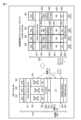
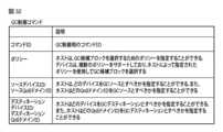
図2は、従来型SSDとホストとの間の役割分担と、本実施形態のフラッシュストレージデバイス3とホスト2との間の役割分担とを示す。Figure 2 shows the division of roles between a conventional SSD and a host, and the division of roles between the
図2の左部は、従来型SSDと仮想ディスクサービスを実行するホストとを含む計算機システム全体の階層構造を表している。The left part of Figure 2 shows the hierarchical structure of the entire computer system, including a conventional SSD and a host running a virtual disk service.
ホスト(サーバ)においては、複数のエンドユーザに複数の仮想マシンを提供するための仮想マシンサービス101が実行される。仮想マシンサービス101上の各仮想マシンにおいては、対応するエンドユーザによって使用されるオペレーティングシステムおよびユーザアプリケーション102が実行される。A
また、ホスト(サーバ)においては、複数のユーザアプリケーション102に対応する複数の仮想ディスクサービス103が実行される。各仮想ディスクサービス103は、従来型SSD内のストレージリソースの容量の一部を、対応するユーザアプリケーション102用のストレージリソース(仮想ディスク)として割り当てる。各仮想ディスクサービス103においては、アプリケーションレベルアドレス変換テーブルを使用して、アプリケーションレベルの論理アドレスをSSD用の論理アドレスに変換するアプリケーションレベルアドレス変換も実行される。さらに、ホストにおいては、アプリケーションレベルGC104も実行される。In addition, in the host (server), multiple
ホスト(サーバ)から従来型SSDへのコマンドの送信および従来型SSDからホスト(サーバ)へのコマンド完了のレスポンスの返送は、ホスト(サーバ)および従来型SSDの各々に存在するI/Oキュー200を介して実行される。The sending of commands from the host (server) to the conventional SSD and the return of command completion responses from the conventional SSD to the host (server) are performed via an I/
従来型SSDは、ライトバッファ(WB)301、ルックアップテーブル(LUT)302、ガベージコレクション機能303、NAND型フラッシュメモリ(NANDフラッシュアレイ)304を含む。従来型SSDは、一つのルックアップテーブル(LUT)302のみを管理しており、NAND型フラッシュメモリ(NANDフラッシュアレイ)304のリソースは複数の仮想ディスクサービス103によって共有される。A conventional SSD includes a write buffer (WB) 301, a lookup table (LUT) 302, a
この構成においては、仮想ディスクサービス103下のアプリケーションレベルGC104と従来型SSD内のガベージコレクション機能303(LUTレベルGC)とを含む重複したGCにより、ライトアンプリフィケーションが大きくなる。また、従来型SSDにおいては、あるエンドユーザまたはある仮想ディスクサービス103からのデータ書き込み量の増加によってGCの頻度が増加し、これによって他のエンドユーザまたは他の仮想ディスクサービス103に対するI/O性能が劣化するというノイジーネイバー問題が生じうる。In this configuration, write amplification increases due to overlapping GCs including the
また、各仮想ディスクサービス内のアプリケーションレベルアドレス変換テーブルと従来型SSD内のLUT302とを含む重複したリソースの存在により、多くのメモリリソースが消費される。In addition, the existence of overlapping resources, including the application level address translation table in each virtual disk service and the
図2の右部は、本実施形態のフラッシュストレージデバイス3とホスト2とを含む計算機システム全体の階層構造を表している。The right part of Figure 2 shows the hierarchical structure of the entire computer system including the
ホスト(サーバ)2においては、複数のエンドユーザに複数の仮想マシンを提供するための仮想マシンサービス401が実行される。仮想マシンサービス401上の各仮想マシンにおいては、対応するエンドユーザによって使用されるオペレーティングシステムおよびユーザアプリケーション402が実行される。A
また、ホスト(サーバ)2においては、複数のユーザアプリケーション402に対応する複数のI/Oサービス403が実行される。これらI/Oサービス403には、LBAベースのブロックI/Oサービス、キー・バリュー・ストアサービスなどが含まれてもよい。各I/Oサービス403は、論理アドレスそれぞれとフラッシュストレージデバイス3の物理アドレスそれぞれとの間のマッピングを管理するルックアップテーブル(LUT)を含む。ここで、論理アドレスとは、アクセス対象のデータを識別可能な識別子を意味する。この論理アドレスは、論理アドレス空間上の位置を指定する論理ブロックアドレス(LBA)であってもよいし、あるいは、キー・バリュー・ストアのキー(タグ)であってもよい。In addition, in the host (server) 2, multiple I/
LBAベースのブロックI/Oサービスにおいては、論理アドレス(LBA)それぞれとフラッシュストレージデバイス3の物理アドレスそれぞれとの間のマッピングを管理するLUTが使用されてもよい。In an LBA-based block I/O service, a LUT may be used that manages the mapping between each logical address (LBA) and each physical address of the
キー・バリュー・ストアサービスにおいては、論理アドレス(つまり、キーのようなタグ)それぞれとこれら論理アドレス(つまり、キーのようなタグ)に対応するデータが格納されているフラッシュストレージデバイス3の物理アドレスそれぞれとの間のマッピングを管理するLUTが使用されてもよい。このLUTにおいては、タグと、このタグによって識別されるデータが格納されている物理アドレスと、このデータのデータ長との対応関係が管理されてもよい。In the key-value store service, a LUT may be used that manages the mapping between each logical address (i.e., a key-like tag) and each physical address of the
各エンドユーザは、使用すべきアドレッシング方法(LBA、キー・バリュー・ストアのキー、等)を選択することができる。Each end user can choose which addressing method to use (LBA, key-value store key, etc.).
これら各LUTは、ユーザアプリケーション402からの論理アドレスそれぞれをフラッシュストレージデバイス3用の論理アドレスそれぞれに変換するのではなく、ユーザアプリケーション402からの論理アドレスそれぞれをフラッシュストレージデバイス3の物理アドレスそれぞれに変換する。つまり、これら各LUTは、フラッシュストレージデバイス3用の論理アドレスを物理アドレスに変換するテーブルとアプリケーションレベルアドレス変換テーブルとが統合(マージ)されたテーブルである。Each of these LUTs does not convert each logical address from the
ホスト(サーバ)2においては、上述のQoSドメイン毎にI/Oサービス403が存在する。あるQoSドメインに属するI/Oサービス403は、対応するQoSドメイン内のユーザアプリケーション402によって使用される論理アドレスそれぞれと対応するQoSドメインに割り当てられたリソースグループに属するブロック群の物理アドレスそれぞれとの間のマッピングを管理する。In the host (server) 2, an I/
ホスト(サーバ)2からフラッシュストレージデバイス3へのコマンドの送信およびフラッシュストレージデバイス3からホスト(サーバ)2へのコマンド完了のレスポンス等の返送は、ホスト(サーバ)2およびフラッシュストレージデバイス3の各々に存在するI/Oキュー500を介して実行される。これらI/Oキュー500も、複数のQoSドメインに対応する複数のキューグループに分類されていてもよい。The sending of commands from the host (server) 2 to the
フラッシュストレージデバイス3は、複数のQoSドメインに対応する複数のライトバッファ(WB)601、複数のQoSドメインに対応する複数のガベージコレクション(GC)機能602、NAND型フラッシュメモリ(NANDフラッシュアレイ)603を含む。The
この図2の右部に示す構成においては、従来型SSD内のLUT302とアプリケーションレベルアドレス変換テーブルとがI/Oサービス403内の一つのLUTとしてマージされているので、アドレス変換情報の格納のために消費されるメモリリソースの量を低減できる。また、アドレス変換ステージの数が減少するので、I/O性能を向上することが可能となる。In the configuration shown on the right side of Figure 2, the
さらに、アプリケーションレベルGCとLUTレベルGCを含む重複したGCではなく、フラッシュストレージデバイス3のみがGC(ユニファイドGC)のためのデータコピーを実行する。したがって、重複したGCが実行される構成に比し、システム全体のライトアンプリフィケーションを大幅に低減することが可能となる。この結果、I/O性能を改善することができ、且つフラッシュストレージデバイス3の寿命を最大化することが可能となる。Furthermore, only the
図3は、図1のシステム構成の変形例を示す。Figure 3 shows a modified example of the system configuration in Figure 1.
図3においては、複数のホスト2Aと複数のフラッシュストレージデバイス3との間のデータ転送がネットワーク機器(ここでは、ネットワークスイッチ1)を介して実行される。In FIG. 3, data transfer between
すなわち、図3の計算機システムにおいては、図1のサーバ2のストレージ管理機能がマネージャ2Bに移され、且つサーバ2のフロントエンド機能が複数のホスト(エンドユーザサービス用ホスト)2Aに移されている。In other words, in the computer system of FIG. 3, the storage management function of the
マネージャ2Bは、複数のフラッシュストレージデバイス3を管理し、各ホスト(エンドユーザサービス用ホスト)2Aからの要求に応じて、これらフラッシュストレージデバイス3のストレージリソースを各ホスト(エンドユーザサービス用ホスト)2Aに割り当てる。The
各ホスト(エンドユーザサービス用ホスト)2Aは、ネットワークを介して一つ以上のエンドユーザ端末61に接続される。各ホスト(エンドユーザサービス用ホスト)2Aは、上述の統合(マージ)された論理物理アドレス変換テーブルであるルックアップテーブル(LUT)を管理する。各ホスト(エンドユーザサービス用ホスト)2Aは、自身のLUTを使用して、対応するエンドユーザによって使用される論理アドレスそれぞれと自身に割り当てられたリソースの物理アドレスそれぞれとの間のマッピングのみを管理する。したがって、この構成は、システムを容易にスケールアウトすることを可能にする。Each host (host for end-user services) 2A is connected to one or more end-
各ホスト2AのグローバルFTLは、ルックアップテーブル(LUT)を管理する機能、高可用性を実現するための機能、重複排除(De-duplication)機能、QoSポリシー制御機能等を有する。The global FTL of each
マネージャ2Bは、複数のフラッシュストレージデバイス3を管理するための専用のデバイス(計算機)である。マネージャ2Bは、各ホスト2Aから要求された容量分のストレージリソースを予約するグローバルリソース予約機能を有する。さらに、マネージャ2Bは、各フラッシュストレージデバイス3の消耗度を監視するためのウェアー監視機能、予約されたストレージリソース(NANDリソース)を各ホスト2Aに割り当てるNANDリソース割り当て機能、QoSポリシー制御機能、グローバルクロック管理機能、等を有する。The
各フラッシュストレージデバイス3は、ローカルFTLを有する。このローカルFTLは、各ホスト2AのグローバルFTLと連携するための機能である。このローカルFTLは、QoS制御機能、各QoSドメインのライトバッファを管理する機能、QoSドメイン内でまたはQoSドメイン間でGCデータコピーを実行する機能、リカバリのためのLUTコピー機能、重複排除(De-duplication)のために使用される参照カウントを管理する機能、ワークロード解析機能、ハウスキーピング機能、等を含んでいてもよい。Each
図3のシステム構成によれば、各フラッシュストレージデバイス3の管理はマネージャ2Bによって実行されるので、各ホスト2Aは、自身に割り当てられた一つ以上のフラッシュストレージデバイス3にI/O要求を送信する動作と、フラッシュストレージデバイス3からのレスポンスを受信するという動作とのみを実行すればよい。つまり、複数のホスト2Aと複数のフラッシュストレージデバイス3との間のデータ転送はスイッチ1のみを介して実行され、マネージャ2Bはこのデータ転送には関与しない。また、上述したように、ホスト2Aそれぞれによって管理されるLUTの内容は互いに独立している。よって、容易にホスト2Aの数を増やすことができるので、スケールアウト型のシステム構成を実現することができる。According to the system configuration of FIG. 3, management of each
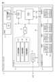
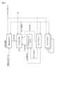
図4は、フラッシュストレージデバイス3の構成例を示す。Figure 4 shows an example configuration of a
フラッシュストレージデバイス3は、コントローラ4および不揮発性メモリ(NAND型フラッシュメモリ)5を備える。フラッシュストレージデバイス3は、ランダムアクセスメモリ、例えば、DRAM6も備えていてもよい。The
NAND型フラッシュメモリ5は、マトリクス状に配置された複数のメモリセルを含むメモリセルアレイを含む。NAND型フラッシュメモリ5は、2次元構造のNAND型フラッシュメモリであってもよいし、3次元構造のNAND型フラッシュメモリであってもよい。The
NAND型フラッシュメモリ5のメモリセルアレイは、複数のブロックBLK0~BLKm-1を含む。ブロックBLK0~BLKm-1の各々は多数のページ(ここではページP0~Pn-1)によって編成される。ブロックBLK0~BLKm-1は、消去単位として機能する。ブロックは、「消去ブロック」、「物理ブロック」、または「物理消去ブロック」と称されることもある。ページP0~Pn-1の各々は、同一ワード線に接続された複数のメモリセルを含む。ページP0~Pn-1は、データ書き込み動作およびデータ読み込み動作の単位である。The memory cell array of the
コントローラ4は、Toggle、オープンNANDフラッシュインタフェース(ONFI)のようなNANDインタフェース13を介して、不揮発性メモリであるNAND型フラッシュメモリ5に電気的に接続されている。コントローラ4は、NAND型フラッシュメモリ5を制御するように構成されたメモリコントローラ(制御回路)である。The
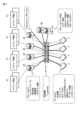
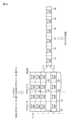
NAND型フラッシュメモリ5は、図5に示すように、複数のNAND型フラッシュメモリダイを含む。各NAND型フラッシュメモリダイは、複数のブロックBLKを含むメモリセルアレイとこのメモリセルアレイを制御する周辺回路とを含む不揮発性メモリダイである。個々のNAND型フラッシュメモリダイは独立して動作可能である。このため、NAND型フラッシュメモリダイは、並列動作単位として機能する。NAND型フラッシュメモリダイは、「NAND型フラッシュメモリチップ」または「不揮発性メモリチップ」とも称される。図5においては、NANDインタフェース13に16個のチャンネルCh1、Ch2、…Ch16が接続されており、これらチャンネルCh1、Ch2、…Ch16の各々に、同数(例えばチャンネル当たり2個のダイ)のNAND型フラッシュメモリダイそれぞれが接続されている場合が例示されている。各チャンネルは、対応するNAND型フラッシュメモリダイと通信するための通信線(メモリバス)を含む。As shown in FIG. 5, the
コントローラ4は、チャンネルCh1、Ch2、…Ch16を介してNAND型フラッシュメモリダイ#1~#32を制御する。コントローラ4は、チャンネルCh1、Ch2、…Ch16を同時に駆動することができる。The
チャンネルCh1~Ch16に接続された16個のNAND型フラッシュメモリダイ#1~#16は第1のバンクとして編成されてもよく、またチャンネルCh1~Ch16に接続された残りの16個のNAND型フラッシュメモリダイ#17~#32は第2のバンクとして編成されてもよい。バンクは、複数のメモリモジュールをバンクインタリーブによって並列動作させるための単位として機能する。図5の構成例においては、16チャンネルと、2つのバンクを使用したバンクインタリーブとによって、最大32個のNAND型フラッシュメモリダイを並列動作させることができる。The 16 NAND flash memory dies #1 to #16 connected to channels Ch1 to Ch16 may be organized as a first bank, and the remaining 16 NAND flash memory dies #17 to #32 connected to channels Ch1 to Ch16 may be organized as a second bank. A bank functions as a unit for operating multiple memory modules in parallel by bank interleaving. In the configuration example of FIG. 5, a maximum of 32 NAND flash memory dies can be operated in parallel by using 16 channels and bank interleaving using two banks.
本実施形態では、コントローラ4は、各々が複数のブロックBLKから構成される複数のブロック(以下、スーパーブロックと称する)を管理してもよく、スーパーブロックの単位で消去動作を実行してもよい。In this embodiment, the
スーパーブロックは、これに限定されないが、NAND型フラッシュメモリダイ#1~#32から一つずつ選択される計32個のブロックBLKを含んでいてもよい。なお、NAND型フラッシュメモリダイ#1~#32の各々はマルチプレーン構成を有していてもよい。例えば、NAND型フラッシュメモリダイ#1~#32の各々が、2つのプレーンを含むマルチプレーン構成を有する場合には、一つのスーパーブロックは、NAND型フラッシュメモリダイ#1~#32に対応する64個のプレーンから一つずつ選択される計64個のブロックBLKを含んでいてもよい。図6には、一つのスーパーブロックSBが、NAND型フラッシュメモリダイ#1~#32から一つずつ選択される計32個のブロックBLK(図5においては太枠で囲まれているブロックBLK)から構成される場合が例示されている。Although not limited to this, the superblock may include a total of 32 blocks BLK selected one by one from the NAND flash memory dies #1 to #32. Each of the NAND flash memory dies #1 to #32 may have a multi-plane configuration. For example, if each of the NAND flash memory dies #1 to #32 has a multi-plane configuration including two planes, one superblock may include a total of 64 blocks BLK selected one by one from the 64 planes corresponding to the NAND flash memory dies #1 to #32. FIG. 6 illustrates a case in which one superblock SB is composed of a total of 32 blocks BLK (blocks BLK surrounded by a thick frame in FIG. 5) selected one by one from the NAND flash memory dies #1 to #32.
図4に示されているように、コントローラ4は、ホストインタフェース11、CPU12、NANDインタフェース13、およびDRAMインタフェース14等を含む。これらCPU12、NANDインタフェース13、DRAMインタフェース14は、バス10を介して相互接続される。As shown in FIG. 4, the
このホストインタフェース11は、ホスト2との通信を実行するように構成されたホストインタフェース回路である。このホストインタフェース11は、例えば、PCIeコントローラ(NVMeコントローラ)であってよい。ホストインタフェース11は、ホスト2から様々な要求(コマンド)を受信する。これら要求(コマンド)には、ライト要求(ライトコマンド)、リード要求(リードコマンド)、他の様々な要求(コマンド)が含まれる。The
CPU12は、ホストインタフェース11、NANDインタフェース13、DRAMインタフェース14を制御するように構成されたプロセッサである。CPU12は、フラッシュストレージデバイス3の電源オンに応答してNAND型フラッシュメモリ5または図示しないROMから制御プログラム(ファームウェア)をDRAM6にロードし、そしてこのファームウェアを実行することによって様々な処理を行う。なお、ファームウェアはコントローラ4内の図示しないSRAM上にロードされてもよい。このCPU12は、ホスト2からの様々なコマンドを処理するためのコマンド処理等を実行することができる。CPU12の動作は、CPU12によって実行される上述のファームウェアによって制御される。なお、コマンド処理の一部または全部は、コントローラ4内の専用ハードウェアによって実行してもよい。The
CPU12は、ライト動作制御部21、リード動作制御部22、およびGC動作制御部23として機能することができる。これらライト動作制御部21、リード動作制御部22、およびGC動作制御部23においては、図2の右部に示すシステム構成を実現するためのアプリケーションプログラムインタフェース(API)が実装されている。The
ライト動作制御部21は、論理アドレスを指定するライト要求(ライトコマンド)をホスト2から受信する。論理アドレスは、書き込むべきデータ(ユーザデータ)を識別可能な識別子であり、例えば、LBAであってもよいし、あるいはキー・バリュー・ストアのキーのようなタグであってもよい。ライトコマンドを受信した場合、ライト動作制御部21は、まず、ホスト2からのデータを書き込むべきブロック(書き込み先ブロック)およびこのブロック内の位置(書き込み先位置)を決定する。次いで、ライト動作制御部21は、ホスト2からのデータ(ライトデータ)を、この書き込み先ブロックの書き込み先位置に書き込む。この場合、ライト動作制御部21は、ホスト2からのデータのみならず、このデータとこのデータの論理アドレスの双方を書き込み先ブロックに書き込むことができる。The write
そして、ライト動作制御部21は、指定された論理アドレスと、データ(ライトデータ)が書き込まれたNAND型フラッシュメモリ5内の位置(物理記憶位置)を示す物理アドレスとをホスト2に返す。Then, the write
この場合、この物理アドレスは、(1)この書き込み先ブロックのブロック番号と、(2)この書き込み先ブロック内の書き込み先位置を示すブロック内オフセットとによって表される。ブロック番号は、データが書き込まれたブロックを指定する識別子である。ブロック番号としては、複数のブロック内の任意の一つを一意に識別可能な様々な値を使用し得る。In this case, this physical address is represented by (1) the block number of the destination block, and (2) an offset within the block that indicates the destination position within the destination block. The block number is an identifier that specifies the block to which the data is written. Various values that can uniquely identify any one of multiple blocks can be used as the block number.
ブロック内オフセットは、書き込み先ブロックの先頭から書き込み先位置までのオフセット、つまり書き込み先ブロックの先頭に対する書き込み先位置のオフセットを示す。書き込み先ブロックの先頭から書き込み先位置までのオフセットのサイズは、ページサイズとは異なるサイズを有する粒度(Grain)の倍数で示される。粒度(Grain)は、上述のアクセス単位である。粒度(Grain)のサイズの最大値は、ブロックサイズまでに制限される。換言すれば、ブロック内オフセットは、書き込み先ブロックの先頭から書き込み先位置までのオフセットをページサイズとは異なるサイズを有する粒度の倍数で示す。The offset within a block indicates the offset from the beginning of the destination block to the destination position, that is, the offset of the destination position relative to the beginning of the destination block. The size of the offset from the beginning of the destination block to the destination position is indicated as a multiple of a granularity (Grain) having a size different from the page size. The granularity (Grain) is the access unit described above. The maximum value of the granularity (Grain) size is limited to the block size. In other words, the offset within a block indicates the offset from the beginning of the destination block to the destination position as a multiple of a granularity having a size different from the page size.
粒度(Grain)は、ページサイズよりも小さいサイズを有していてもよい。例えば、ページサイズが16Kバイトである場合、粒度(Grain)は、そのサイズが4Kバイトであってもよい。この場合、ある一つのブロックにおいては、各々サイズが4Kバイトである複数のオフセット位置が規定される。ブロック内の最初のオフセット位置に対応するブロック内オフセットは、例えば0であり、ブロック内の次のオフセット位置に対応するブロック内オフセットは、例えば1である、ブロック内のさらに次のオフセット位置に対応するブロック内オフセットは、例えば2である。The granularity may have a size smaller than the page size. For example, if the page size is 16 Kbytes, the granularity may have a size of 4 Kbytes. In this case, in one block, multiple offset positions are defined, each of which is 4 Kbytes in size. The intra-block offset corresponding to the first offset position in the block is, for example, 0, the intra-block offset corresponding to the next offset position in the block is, for example, 1, and the intra-block offset corresponding to the next offset position in the block is, for example, 2.
あるいは、粒度(Grain)は、ページサイズよりも大きなサイズを有していてもよい。例えば、粒度(Grain)は、ページサイズの数倍のサイズであってもよい。ページサイズが16Kバイトである場合、粒度は、32Kバイトのサイズであってもよい。Alternatively, the grain may have a size larger than the page size. For example, the grain may be several times the size of the page size. If the page size is 16 Kbytes, the grain may be 32 Kbytes in size.
このように、ライト動作制御部21は、データを書き込むべきブロックおよびこのブロック内の位置の双方を自身で決定し、そしてホスト2からのデータ(ユーザデータ)が書き込まれた位置を示す物理アドレスとして、ブロック番号およびページ番号ではなく、ブロック番号およびブロック内オフセットをホスト2に通知する。これにより、ホスト2は、ブロックサイズ、ページ書き込み順序制約、バッドページ、ページサイズ等を意識することなく、ユーザデータをNAND型フラッシュメモリ5に書き込むことができ、さらに、ブロック番号およびブロック内オフセットによって表された物理アドレスを、このユーザデータの論理アドレスにマッピングすることができる。In this way, the write
リード動作制御部22は、物理アドレス(すなわち、ブロック番号およびブロック内オフセット)を指定するリード要求(リードコマンド)をホスト2から受信した場合、これらブロック番号およびブロック内オフセットに基づいてNAND型フラッシュメモリ5からデータをリードする。リード対象のブロックは、ブロック番号によって特定される。このブロック内のリード対象の物理記憶位置は、ブロック内オフセットによって特定される。このブロック内オフセットを使用することにより、ホスト2は、NAND型フラッシュメモリの世代毎の異なるページサイズをハンドリングする必要がない。When the read
リード対象の物理記憶位置を得るために、リード動作制御部22は、まず、このブロック内オフセットを、ページサイズを表す粒度の数(ここでは、4)で除算し、そしてこの除算によって得られる商および余りを、リード対象のページ番号およびリード対象のページ内オフセットとしてそれぞれ決定してもよい。To obtain the physical memory location of the read target, the read
GC動作制御部23は、NAND型フラッシュメモリ5のガベージコレクションを実行する場合、このガベージコレクションのためのコピー元ブロック(GCソースブロック)およびコピー先ブロック(GCデスティネーションブロック)をNAND型フラッシュメモリ5内の多数のブロックから選択する。この場合、GC動作制御部23は、通常、複数のコピー元ブロック(GCソースブロック)と、一つ以上のコピー先ブロック(GCデスティネーションブロック)とを選択する。コピー元ブロック(GCソースブロック)を選択するための条件(GCポリシー)は、ホスト2によって指定されてもよい。例えば、有効データ量が最も少ないブロックをコピー元ブロック(GCソースブロック)として優先的に選択するというGCポリシーが使用されてもよいし、別のGCポリシーが使用されてもよい。このように、コピー元ブロック(GCソースブロック)およびコピー先ブロック(GCデスティネーションブロック)の選択は、ホスト2ではなく、フラッシュストレージデバイス3のコントローラ4(GC動作制御部23)によって実行される。コントローラ4は、各ブロック管理テーブルを使用して、各ブロックの有効データ量を管理してもよい。When the GC
ガベージコレクションのコピー元グループ(ソースQosドメイン)およびコピー先グループ(デスティネーションQosドメイン)を指定するコマンド(GC制御コマンド)をホスト2から受信した場合、GC動作制御部23は、コピー元グループに属するブロック群からガベージコレクションのコピー元ブロックを選択し、コピー先グループに属するブロック群からガベージコレクションのコピー先ブロックを選択する。When a command (GC control command) that specifies the source group (source Qos domain) and destination group (destination Qos domain) for garbage collection is received from the
有効データ/無効データの管理は、ブロック管理テーブル32を使用して実行されてもよい。このブロック管理テーブル32は、例えば、ブロック毎に存在してもよい。あるブロックに対応するブロック管理テーブル32においては、このブロック内のデータそれぞれの有効/無効を示すビットマップフラグが格納されている。ここで、有効データとは、LUTから参照されているデータ(すなわち論理アドレスから最新のデータとして紐付けられているデータ)であって、後にホスト2からリードされる可能性があるデータを意味する。無効データとは、もはやホスト2からリードされる可能性が無いデータを意味する。例えば、ある論理アドレスに関連付けられているデータは有効データであり、どの論理アドレスにも関連付けられていないデータは無効データである。Management of valid data/invalid data may be performed using a block management table 32. This block management table 32 may exist for each block, for example. In the block management table 32 corresponding to a certain block, a bitmap flag indicating whether each piece of data in this block is valid/invalid is stored. Here, valid data means data referenced by the LUT (i.e., data linked to a logical address as the latest data) and data that may be read by the
GC動作制御部23は、コピー元ブロック(GCソースブロック)内に格納されている有効データを書き込むべきコピー先ブロック(GCデスティネーションブロック)内の位置(コピー先位置)を決定し、有効データをコピー先ブロック(GCデスティネーションブロック)のこの決定された位置(コピー先位置)にコピーする。この場合、GC動作制御部23は、有効データとこの有効データの論理アドレスの双方を、コピー先ブロック(GCデスティネーションブロック)にコピーしてもよい。GC動作制御部23は、コピー元ブロック(GCソースブロック)に対応するブロック管理テーブル32を参照することによってGCソースブロック内の有効データを特定してもよい。あるいは、別の実施形態では、有効データ/無効データの管理がホスト2によって実行されてもよい。この場合には、GC動作制御部23は、GCソースブロック内の各データの有効/無効を示す情報をホスト2から受信し、この受信した情報に基づいて、GCソースブロック内の有効データを特定してもよい。The GC
そして、GC動作制御部23は、コピーされた有効データの論理アドレスと、コピー先ブロック(GCデスティネーションブロック)のブロック番号と、コピー先ブロック(GCデスティネーションブロック)の先頭からコピー先位置までのオフセットを上述の粒度の倍数で示すブロック内オフセットとをホスト2に通知する。Then, the GC
本実施形態では、上述したように、ライト動作制御部21は、ホスト2からのデータ(ライトデータ)とホスト2からの論理アドレスの双方を書き込み先ブロックに書き込むことができる。このため、GC動作制御部23は、コピー元ブロック(GCソースブロック)内の各データの論理アドレスをこのコピー元ブロック(GCソースブロック)から容易に取得することができるので、コピーされた有効データの論理アドレスをホスト2に容易に通知することができる。In this embodiment, as described above, the write
NANDインタフェース13は、CPU12の制御の下、NAND型フラッシュメモリ5を制御するように構成されたメモリ制御回路である。DRAMインタフェース14は、CPU12の制御の下、DRAM6を制御するように構成されたDRAM制御回路である。DRAM6の記憶領域の一部は、ライトバッファ(WB)31の格納のために使用される。また、DRAM6の記憶領域の他の一部は、ブロック管理テーブル32の格納のために使用される。なお、これらライトバッファ(WB)31およびブロック管理テーブル32は、コントローラ4内の図示しないSRAMに格納されてもよい。The
図7は、フラッシュストレージデバイス3に適用されるライトコマンドを示す。Figure 7 shows a write command applied to
ライトコマンドは、フラッシュストレージデバイス3にデータの書き込みを要求するコマンドである。このライトコマンドは、コマンドID、QoSドメインID、論理アドレス、長さ、等を含んでもよい。The write command is a command that requests writing of data to the
コマンドIDはこのコマンドがライトコマンドであることを示すID(コマンドコード)であり、ライトコマンドにはライトコマンド用のコマンドIDが含まれる。The command ID is an ID (command code) that indicates that this command is a write command, and the write command includes a command ID for the write command.
QoSドメインIDは、データが書き込まれるべきQoSドメインを一意に識別可能な識別子である。あるエンドユーザからのライト要求に応じてホスト2から送信されるライトコマンドは、このエンドユーザに対応するQoSドメインを指定するQoSドメインIDを含んでもよい。ネームスペースIDがQoSドメインIDとして扱われてもよい。The QoS domain ID is an identifier that can uniquely identify the QoS domain to which data is to be written. A write command sent from the
論理アドレスは、書き込まれるべきライトデータを識別するための識別子である。この論理アドレスは、上述したように、LBAであってもよいし、キー・バリュー・ストアのキーであってもよい。論理アドレスがLBAである場合には、このライトコマンドに含まれる論理アドレス(開始LBA)は、ライトデータが書き込まれるべき論理位置(最初の論理位置)を示す。The logical address is an identifier for identifying the write data to be written. As described above, this logical address may be an LBA or a key of a key-value store. If the logical address is an LBA, the logical address (start LBA) included in this write command indicates the logical location (first logical location) where the write data should be written.
長さは、書き込まれるべきライトデータの長さを示す。この長さ(データ長)は、粒度(Grain)の数によって指定されてもよいし、LBAの数によって指定されてもよいし、あるいはそのサイズがバイトによって指定されてもよい。The length indicates the length of the write data to be written. This length (data length) may be specified by the number of grains, the number of LBAs, or the size may be specified by bytes.
上述したように、コントローラ4は、NAND型フラッシュメモリ5内の多数のブロックの各々が一つのグループのみに属するようにNAND型フラッシュメモリ5内の多数のブロックを複数のグループ(複数のQoSドメイン)に分類することができる。そして、コントローラ4は、グループ(QoSドメイン)毎に、フリーブロックリスト(フリーブロックプール)とアクティブブロックリスト(アクティブブロックプール)とを管理することができる。As described above, the
各ブロックの状態は、有効データを格納しているアクティブブロックと、有効データを格納していないフリーブロックとに大別される。アクティブブロックである各ブロックは、アクティブブロックリストによって管理される。一方、フリーブロックである各ブロックは、フリーブロックリストによって管理される。The state of each block is broadly classified into active blocks, which store valid data, and free blocks, which do not store valid data. Active blocks are managed by the active block list. On the other hand, free blocks are managed by the free block list.
ホスト2からライトコマンドを受信した時、コントローラ4は、ホスト2からのデータが書き込まれるべきブロック(書き込み先ブロック)およびこの書き込み先ブロック内の位置(書き込み先位置)を決定する。コントローラ4は、QoSドメインIDに対応するQoSドメインに属するフリーブロック群の一つを書き込み先ブロックとして決定してもよい。書き込み先位置は、ページ書き込み順序の制約およびバッドページ等を考慮して決定される。そして、コントローラ4は、ホスト2からのデータを、書き込み先ブロック内の書き込み先位置に書き込む。When a write command is received from the
なお、この書き込み先ブロック全体がユーザデータで満たされたならば、コントローラ4は、この書き込み先ブロックをアクティブブロックリスト(アクティブブロックプール)に移動する。そして、コントローラ4は、このQoSドメインに対応するフリーブロックリストからフリーブロックを再び選択し、この選択したフリーブロックを新たな書き込み先ブロックとして割り当てる。When the entire destination block is filled with user data, the
もしフリーブロックリストによって管理されている残りフリーブロックの数が所定のポリシーによって定められる閾値以下に低下した場合あるいはホスト2からガベージコレクションを実施する指示があった場合、コントローラ4は、このQoSドメインのガベージコレクションを開始してもよい。If the number of remaining free blocks managed by the free block list falls below a threshold defined by a specified policy, or if the
このQoSドメインのガベージコレクションでは、コントローラ4は、このQoSドメインに対応するアクティブブロック群からコピー元ブロック(GCソースブロック)とコピー先ブロック(GCデスティネーションブロック)を選択する。どのブロックをGC候補(コピー元ブロック)として選択するかは、ホスト2によって指定される上述のポリシーに従って決定されてもよいし、ホスト2から指定されても良い。ポリシーも基づく場合には例えば、有効データ量が最も少ないブロックがGC候補(コピー元ブロック)として選択されてもよい。In garbage collection of this QoS domain, the
図8は、図7のライトコマンドに対するレスポンスを示す。Figure 8 shows the response to the write command in Figure 7.
このレスポンスは、論理アドレス、物理アドレス、長さを含む。This response includes the logical address, physical address, and length.
論理アドレスは、図7のライトコマンドに含まれていた論理アドレスである。The logical address is the logical address included in the write command in Figure 7.
物理アドレスは、図7のライトコマンドに応じてデータが書き込まれたNAND型フラッシュメモリ5内の物理記憶位置を示す。本実施形態では、この物理アドレスは、ブロック番号とページ番号との組み合わせではなく、上述したように、ブロック番号とオフセット(ブロック内オフセット)との組み合わせによって指定される。ブロック番号は、フラッシュストレージデバイス3内の全てのブロックの任意の一つを一意に識別可能な識別子である。全てのブロックに異なるブロック番号が付与されている場合には、これらブロック番号を直接使用してもよい。あるいは、ブロック番号は、ダイ番号と、ダイ内ブロック番号との組み合わせによって表現されてもよい。長さは、書き込まれるべきライトデータの長さを示す。この長さ(データ長)は、粒度(Grain)の数によって指定されてもよいし、LBAの数によって指定されてもよいし、あるいはそのサイズがバイトによって指定されてもよい。The physical address indicates the physical storage location in the
図9は、フラッシュストレージデバイス3に適用されるTrimコマンドを示す。Figure 9 shows the Trim command applied to
このTrimコマンドは、無効にすべきデータが格納されている物理記憶位置を示すブロック番号およびブロック内オフセットを含むコマンドである。つまり、このTrimコマンドは、LBAのような論理アドレスではなく、物理アドレスを指定可能である。このTrimコマンドは、コマンドID、物理アドレス、長さを含む。This Trim command includes a block number and an offset within the block that indicate the physical memory location where the data to be invalidated is stored. In other words, this Trim command can specify a physical address rather than a logical address such as an LBA. This Trim command includes a command ID, a physical address, and a length.
コマンドIDはこのコマンドがTrimコマンドであることを示すID(コマンドコード)であり、TrimコマンドにはTrimコマンド用のコマンドIDが含まれる。The command ID is an ID (command code) that indicates that this command is a Trim command, and the Trim command includes a command ID for the Trim command.
物理アドレスは、無効化すべきデータが格納されている最初の物理記憶位置を示す。本実施形態では、この物理アドレスは、ブロック番号とオフセット(ブロック内オフセット)との組み合わせによって指定される。The physical address indicates the first physical memory location where the data to be invalidated is stored. In this embodiment, this physical address is specified by a combination of a block number and an offset (offset within the block).
長さは、無効化すべきデータの長さを示す。この長さ(データ長)は、粒度(Grain)の数によって指定されてもよいし、バイトによって指定されてもよい。The length indicates the length of the data to be invalidated. This length (data length) may be specified by the number of grains or by bytes.
コントローラ4は、複数のブロックの各々に含まれるデータそれぞれの有効/無効を示すフラグ(ビットマップフラグ)をブロック管理テーブル32を使用して管理する。無効にすべきデータが格納されている物理記憶位置を示すブロック番号およびオフセット(ブロック内オフセット)を含むTrimコマンドをホスト2から受信した場合、コントローラ4は、ブロック管理テーブル32を更新して、Trimコマンドに含まれるブロック番号およびブロック内オフセットに対応する物理記憶位置のデータに対応するフラグ(ビットマップフラグ)を無効を示す値に変更する。The
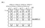
図10は、物理アドレスを規定するブロック番号およびオフセットを示す。Figure 10 shows the block number and offset that define the physical address.
ブロック番号はある一つのブロックBLKを指定する。各ブロックBLKは、図10に示されているように、複数のページ(ここでは、ページ0~ページn)を含む。The block number specifies a block BLK. Each block BLK contains multiple pages (here,
ページサイズ(各ページのユーザデータ格納領域)が16Kバイトであり、粒度(Grain)が4KBのサイズであるケースにおいては、このブロックBLKは、4×(n+1)個の領域に論理的に分割される。When the page size (user data storage area of each page) is 16 KB and the granularity is 4 KB, this block BLK is logically divided into 4 x (n + 1) areas.
オフセット+0はページ0の最初の4KB領域を示し、オフセット+1はページ0の2番目の4KB領域を示し、オフセット+2はページ0の3番目の4KB領域を示し、オフセット+3はページ0の4番目の4KB領域を示す。Offset +0 points to the first 4KB area of
オフセット+4はページ1の最初の4KB領域を示し、オフセット+5はページ1の2番目の4KB領域を示し、オフセット+6はページ1の3番目の4KB領域を示し、オフセット+7はページ1の4番目の4KB領域を示す。Offset +4 points to the first 4KB area on
図11は、ライトコマンドに応じて実行される書き込み動作とこのライトコマンドに対するレスポンスに含まれる返値との関係を示す。Figure 11 shows the relationship between the write operation performed in response to a write command and the return value included in the response to this write command.
フラッシュストレージデバイス3のコントローラ4は、有効データを含まないフリーブロック群をフリーブロックリストによって管理しており、これらフリーブロック群から一つのブロック(フリーブロック)を選択し、選択したブロックを書き込み先ブロックとして割り当てる。いま、ブロックBLK#1が書き込み先ブロックとして割り当てられた場合を想定する。コントローラ4は、ページ0、ページ1、ページ2、…ページnという順序で、データをページ単位でブロックBLK#1に書き込む。The
図11においては、ブロックBLK#1のページ0に16Kバイト分のデータがすでに書き込まれている状態で、論理アドレス(LBAx)および長さ(=4)を指定するライトコマンドがホスト2から受信された場合が想定されている。コントローラ4は、ブロックBLK#1のページ1を書き込み先位置として決定し、ホスト2から受信される16Kバイト分のライトデータをブロックBLK#1のページ1に書き込む。そして、コントローラ4は、このライトコマンドに対するレスポンス(論理アドレス、ブロック番号、オフセット(ブロック内オフセット)、長さ)をホスト2に返す。このケースにおいては、論理アドレスはLBAxであり、ブロック番号はBLK#1であり、オフセット(ブロック内オフセット)は+5であり、長さは4である。In FIG. 11, it is assumed that 16 Kbytes of data has already been written to
図12は、不良ページ(バッドページ)をスキップする書き込み動作を示す。Figure 12 shows a write operation that skips a bad page.
図12においては、ブロックBLK#1のページ0、ページ1にデータがすでに書き込まれている状態で、論理アドレス(LBAx+1)および長さ(=4)を指定するライトコマンドがホスト2から受信された場合が想定されている。もしブロックBLK#1のページ2が不良ページであるならば、コントローラ4は、ブロックBLK#1のページ3を書き込み先位置として決定し、ホスト2から受信される16Kバイト分のライトデータをブロックBLK#1のページ3に書き込む。そして、コントローラ4は、このライトコマンドに対するレスポンス(論理アドレス、ブロック番号、オフセット(ブロック内オフセット)、長さ)をホスト2に返す。このケースにおいては、論理アドレスはLBAx+1であり、ブロック番号はBLK#1であり、オフセット(ブロック内オフセット)は+12であり、長さは4である。In FIG. 12, it is assumed that data has already been written to
図13は、不良ページをスキップする書き込み動作の別の例を示す。Figure 13 shows another example of a write operation that skips a bad page.
図13においては、不良ページを挟む2つのページに跨がってデータが書き込まれる場合が想定されている。いま、ブロックBLK#2のページ0、ページ1にデータがすでに書き込まれており、且つライトバッファ31に未書き込みの8Kバイト分のライトデータが残っている場合を想定する。この状態で、論理アドレス(LBAy)および長さ(=6)を指定するライトコマンドが受信されたならば、コントローラ4は、未書き込みの8Kバイトライトデータと、ホスト2から新たに受信される24Kバイトライトデータ内の最初の8Kバイトライトデータとを使用して、ページサイズに対応する16Kバイトライトデータを準備する。そして、コントローラ4は、この準備した16KバイトライトデータをブロックBLK#2のページ2に書き込む。In FIG. 13, it is assumed that data is written across two pages, one of which is a defective page. Assume that data has already been written to
もしブロックBLK#2の次のページ3が不良ページであるならば、コントローラ4は、ブロックBLK#2のページ4を次の書き込み先位置として決定し、ホスト2から受信された24Kバイトライトデータ内の残りの16Kバイトライトデータを、ブロックBLK#2のページ4に書き込む。If the
そして、コントローラ4は、このライトコマンドに対するレスポンス(論理アドレス、ブロック番号、オフセット(ブロック内オフセット)、長さ)をホスト2に返す。このケースにおいては、このレスポンスは、LBAy、ブロック番号(=BLK#2)、オフセット(=+10)、長さ(=2)、ブロック番号(=BLK#2)、オフセット(=+16)、長さ(=4)を含んでもよい。Then, the
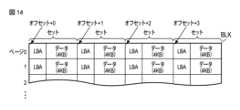
図14、図15は、論理アドレスとデータのペアをブロック内のページに書き込む動作を示す。Figures 14 and 15 show the operation of writing a logical address and data pair to a page in a block.
各ブロックにおいて、各ページは、ユーザデータを格納するためのユーザデータ領域と管理データを格納するための冗長領域とを含んでもよい。ページサイズは16KB+アルファである。In each block, each page may include a user data area for storing user data and a redundant area for storing management data. The page size is 16KB+alpha.
コントローラ4は、4KBユーザデータとこの4KBユーザデータに対応する論理アドレス(例えばLBA)との双方を書き込み先ブロックBLKに書き込む。この場合、図14に示すように、各々がLBAと4KBユーザデータとを含む4つのデータセットが同じページに書き込まれてもよい。ブロック内オフセットは、セット境界を示してもよい。The
あるいは、図15に示されているように、4つの4KBユーザデータがページ内のユーザデータ領域に書き込まれ、これら4つの4KBユーザデータに対応する4つのLBAがこのページ内の冗長領域に書き込まれてもよい。Alternatively, as shown in FIG. 15, four 4 KB user data may be written to the user data area in a page, and four LBAs corresponding to these four 4 KB user data may be written to the redundant area in the page.
図16は、スーバーブロックが使用されるケースにおけるブロック番号とオフセット(ブロック内オフセット)との関係を示す。以下では、ブロック内オフセットは単にオフセットとしても参照される。Figure 16 shows the relationship between block number and offset (offset within block) in the case where superblocks are used. In the following, the offset within block is also referred to simply as offset.
ここでは、図示を簡単化するために、ある一つのスーパーブロックSB#1が4つのブロックBLK#11、BLK#21、BLK#31、BLK#41から構成されている場合が想定されている。コントローラ4は、ブロックBLK#11のページ0、ブロックBLK#21のページ0、ブロックBLK#31のページ0、ブロックBLK#41のページ0、ブロックBLK#11のページ1、ブロックBLK#21のページ1、ブロックBLK#31のページ1、ブロックBLK#41のページ1、…という順序でデータを書き込む。To simplify the illustration, it is assumed here that one
オフセット+0はブロックBLK#11のページ0の最初の4KB領域を示し、オフセット+1はブロックBLK#11のページ0の2番目の4KB領域を示し、オフセット+2はブロックBLK#11のページ0の3番目の4KB領域を示し、オフセット+3はブロックBLK#11のページ0の4番目の4KB領域を示す。Offset +0 indicates the first 4KB area of
オフセット+4はブロックBLK#21のページ0の最初の4KB領域を示し、オフセット+5はブロックBLK#21のページ0の2番目の4KB領域を示し、オフセット+6はブロックBLK#21のページ0の3番目の4KB領域を示し、オフセット+7はブロックBLK#21のページ0の4番目の4KB領域を示す。Offset +4 indicates the first 4KB area of
同様に、オフセット+12はブロックBLK#41のページ0の最初の4KB領域を示し、オフセット+13はブロックBLK#41のページ0の2番目の4KB領域を示し、オフセット+14はブロックBLK#41のページ0の3番目の4KB領域を示し、オフセット+15はブロックBLK#41のページ0の4番目の4KB領域を示す。Similarly, offset +12 points to the first 4KB area of
オフセット+16はブロックBLK#11のページ1の最初の4KB領域を示し、オフセット+17はブロックBLK#11のページ1の2番目の4KB領域を示し、オフセット+18はブロックBLK#11のページ1の3番目の4KB領域を示し、オフセット+19はブロックBLK#11のページ1の4番目の4KB領域を示す。Offset +16 indicates the first 4KB area of
オフセット+20はブロックBLK#21のページ1の最初の4KB領域を示し、オフセット+21はブロックBLK#21のページ1の2番目の4KB領域を示し、オフセット+22はブロックBLK#21のページ1の3番目の4KB領域を示し、オフセット+23はブロックBLK#21のページ1の4番目の4KB領域を示す。Offset +20 indicates the first 4KB area of
同様に、オフセット+28はブロックBLK#41のページ1の最初の4KB領域を示し、オフセット+29はブロックBLK#41のページ1の2番目の4KB領域を示し、オフセット+30はブロックBLK#41のページ1の3番目の4KB領域を示し、オフセット+31はブロックBLK#41のページ1の4番目の4KB領域を示す。Similarly, offset +28 indicates the first 4KB region of
例えば、あるLBA(LBAx)を指定するライトコマンドに対応する4Kバイトデータをオフセット+8に対応する位置に書き込んだ場合には、コントローラ4は、論理アドレス(=LBAx)、ブロック番号(=SB#1)、オフセット(=+8)、長さ(=1)をこのライトコマンドに対するレスポンスとしてホスト2に返してもよい。For example, if 4K bytes of data corresponding to a write command specifying a certain LBA (LBAx) are written to a location corresponding to offset +8, the
図17は、ホスト2とフラッシュストレージデバイス3とによって実行される書き込み動作処理のシーケンスを示す。Figure 17 shows the sequence of a write operation process performed by the
ホスト2は、QoSドメインID、LBA、長さを含むライトコマンドをフラッシュストレージデバイス3に送信する。フラッシュストレージデバイス3のコントローラ4がこのライトコマンドを受信した時、コントローラ4は、ホスト2からのライトデータを書き込むべき書き込み先ブロックおよびこの書き込み先ブロック内の位置を決定する。より詳しくは、コントローラ4は、フリーブロックリストから一つのフリーブロックを選択し、選択したフリーブロックを書き込み先ブロックとして割り当てる(ステップS12)。つまり、この選択されたフリーブロックおよびこの選択されたフリーブロック内の利用可能な最初のページが、ホスト2からのライトデータを書き込むべき書き込み先ブロックおよびこの書き込み先ブロック内の位置として決定される。もし書き込み先ブロックがすでに割り当てられている場合には、このステップ12における書き込み先ブロック割り当て処理を実行する必要は無い。すでに割り当てられている書き込み先ブロック内の利用可能な次のページが、ホスト2からのライトデータを書き込むべき書き込み先ブロック内の位置として決定される。The
コントローラ4は、複数のQoSドメインに対応する複数のフリーブロックリストを管理してもよい。あるQoSドメインに対応するフリーブロックリストにおいては、このQoSドメインに対して予約されたブロック群のみが登録されてもよい。この場合、ステップS12では、コントローラ4は、ライトコマンドのQoSドメインIDによって指定されるQoSドメインに対応するフリーブロックリストを選択し、この選択したフリーブロックリストから一つのフリーブロックを選択し、この選択したフリーブロックを書き込み先ブロックとして割り当ててもよい。これにより、異なるQoSドメインに対応するデータが同じブロックに混在されてしまうことを防止することができる。The
コントローラ4は、ホスト2から受信されるライトデータを書き込み先ブロックに書き込む(ステップS12)。ステップS12では、コントローラ4は、論理アドレス(ここではLBA)とライトデータの双方を書き込み先ブロックに書き込む。The
コントローラ4は、ブロック管理テーブル32を更新して、書き込まれたデータに対応するビットマップフラグ(つまり、このデータが書き込まれた物理記憶位置の物理アドレスに対応するビットマップフラグ)を0から1に変更する(ステップS13)。例えば、図18に示されているように、開始LBAがLBAxである16Kバイト更新データがブロックBLK#1のオフセット+4~+7に対応する物理記憶位置に書き込まれた場合を想定する。この場合、図19に示されているように、ブロックBLK#1用のブロック管理テーブルにおいては、オフセット+4~+7に対応するビットマップフラグそれぞれが0から1に変更される。The
コントローラ4は、このライトコマンドに対するレスポンスをホスト2に返す(ステップS14)。例えば、図18に示されているように、開始LBAがLBAxである16Kバイト更新データがブロックBLK#1のオフセット+4~+7に対応する物理記憶位置に書き込まれたならば、LBAx、ブロック番号(=BLK1)、オフセット(=+4)、長さ(=4)を含むレスポンスがコントローラ4からホスト2に送信される。The
ホスト2がこのレスポンスを受信した時、ホスト2は、ホスト2によって管理されているLUTを更新して、書き込まれたライトデータに対応する論理アドレスそれぞれに物理アドレスをマッピングする。図20に示されているように、LUTは、複数の論理アドレス(例えばLBA)それぞれに対応する複数のエントリを含む。ある論理アドレス(例えばあるLBA)に対応するエントリには、このLBAに対応するデータが格納されているNAND型フラッシュメモリ5内の位置(物理記憶位置)を示す物理アドレスPBA、つまりブロック番号、オフセット(ブロック内オフセット)が格納される。図18に示されているように、開始LBAがLBAxである16Kバイト更新データがブロックBLK#1のオフセット+4~+7に対応する物理記憶位置に書き込まれたならば、図20に示されているように、LUTが更新されて、LBAxに対応するエントリにBLK#1、オフセット+4が格納され、LBAx+1に対応するエントリにBLK#1、オフセット+5が格納され、LBAx+2に対応するエントリにBLK#1、オフセット+6が格納され、LBAx+3に対応するエントリにBLK#1、オフセット+7が格納される。When the
この後、ホスト2は、上述の更新データの書き込みによって不要になった以前のデータを無効化するためのTrimコマンドをフラッシュストレージデバイス3に送信する(ステップS21)。図18に示されているように、以前のデータがブロックBLK#0のオフセット+0、オフセット+1、オフセット+2、オフセット+3に対応する位置に格納されている場合には、図21に示すように、ブロック番号(=BLK#0)、オフセット(=+0)、長さ(=4)を指定するTrimコマンドがホスト2からフラッシュストレージデバイス3に送信される。フラッシュストレージデバイス3のコントローラ4は、このTrimコマンドに応じて、ブロック管理テーブル32を更新する(ステップS15)。ステップS15においては、図21に示すように、ブロックBLK#0用のブロック管理テーブルにおいて、オフセット+0~+3に対応するビットマップフラグそれぞれが1から0に変更される。After this, the
図22は、フラッシュストレージデバイス3に適用されるリードコマンドを示す。Figure 22 shows a read command applied to
リードコマンドは、フラッシュストレージデバイス3にデータの読み出しを要求するコマンドである。このリードコマンドは、コマンドID、物理アドレスPBA、長さ、転送先ポインタを含む。The read command is a command that requests the
コマンドIDはこのコマンドがリードコマンドであることを示すID(コマンドコード)であり、リードコマンドにはリードコマンド用のコマンドIDが含まれる。The command ID is an ID (command code) that indicates that this command is a read command, and the read command contains a command ID for the read command.
物理アドレスPBAは、データが読み出されるべき最初の物理記憶位置を示す。物理アドレスPBAは、ブロック番号、オフセット(ブロック内オフセット)によって指定される。The physical address PBA indicates the first physical memory location from which data is to be read. The physical address PBA is specified by the block number and offset (offset within the block).
長さは、リードすべきデータの長さを示す。このデータ長は、Grainの数によって指定可能である。The length indicates the length of the data to be read. This data length can be specified by the number of grains.
転送先ポインタは、読み出されたデータが転送されるべきホスト2内のメモリ上の位置を示す。The destination pointer indicates the location in memory in
一つのリードコマンドは、物理アドレスPBA(ブロック番号、オフセット)と長さの組を複数指定することができる。A single read command can specify multiple pairs of physical address PBA (block number, offset) and length.
図23は、リード動作を示す。Figure 23 shows the read operation.
ここでは、ブロック番号(=BLK#2)、オフセット(=+5)、長さ(=3)を指定するリードコマンドがホスト2から受信された場合が想定されている。フラッシュストレージデバイス4のコントローラ5は、ブロック番号(=BLK#2)、オフセット(=+5)、長さ(=3)に基づいて、BLK#2からデータd1~d3をリードする。この場合、コントローラ4は、BLK#2のページ1から1ページサイズ分のデータをリードし、このリードデータからデータd1~データd3を抽出する。次いで、コントローラ4は、データd1~データd3を、転送先ポインタによって指定されるホストメモリ上に転送する。Here, it is assumed that a read command specifying the block number (=BLK#2), offset (=+5), and length (=3) has been received from the
図24は、ホスト2からのリードコマンドに応じて、異なる物理記憶位置にそれぞれ格納されているデータ部をリードする動作を示す。Figure 24 shows the operation of reading data portions stored in different physical storage locations in response to a read command from
ここでは、ブロック番号(=BLK#2)、オフセット(=+10)、長さ(=2)、ブロック番号(=BLK#2)、オフセット(=+16)、長さ(=4)を指定するリードコマンドがホスト2から受信された場合が想定されている。フラッシュストレージデバイス4のコントローラ5は、ブロック番号(=BLK#2)、オフセット(=+10)、長さ(=2)に基づいて、BLK#2のページ2から1ページサイズ分のデータをリードし、このリードデータからデータd1~データd2を抽出する。次いで、コントローラ5は、ブロック番号(=BLK#2)、オフセット(=+16)、長さ(=4)に基づいて、BLK#2のページ4から1ページサイズ分のデータ(データd3~データd4)をリードする。そして、コントローラ5は、データd1~データd2とデータd3~データd4とを結合することによって得られる長さ(=6)のリードデータを、リードコマンド内の転送先ポインタによって指定されるホストメモリ上に転送する。Here, it is assumed that a read command specifying the block number (=BLK#2), offset (=+10), length (=2), block number (=BLK#2), offset (=+16), and length (=4) is received from the
これにより、たとえブロック内に不良ページが存在する場合であっても、リードエラーを引き起こすことなく、別個の物理記憶位置からデータ部をリードすることができる。また、たとえデータが2つのブロックに跨がって書き込まれている場合であっても、このデータを一つのリードコマンドの発行によってリードすることができる。This allows the data portion to be read from a separate physical memory location without causing a read error, even if a bad page exists in a block. Also, even if data is written across two blocks, this data can be read by issuing a single read command.
図25は、ホスト2とフラッシュストレージデバイス3とによって実行されるリード処理のシーケンスを示す。Figure 25 shows the sequence of a read process performed by the
ホスト2は、ホスト2によって管理されているLUTを参照して、ユーザアプリケーションからのリード要求に含まれる論理アドレスをブロック番号、オフセットに変換する。そして、ホスト2は、このブロック番号、オフセット、長さを指定するリードコマンドをフラッシュストレージデバイス3に送信する。The
フラッシュストレージデバイス3のコントローラ4がリードコマンドをホスト2から受信した時、コントローラ4は、このリードコマンドによって指定されたブロック番号に対応するブロックをリード対象のブロックとして決定するとともに、このリードコマンドによって指定されたオフセットに基づいてリード対象のページを決定する(ステップS31)。ステップS31では、コントローラ4は、まず、リードコマンドによって指定されたオフセットを、ページサイズを表す粒度の数(ここでは、4)で除算してもよい。そして、コントローラ4は、この除算によって得られる商および余りを、リード対象のページ番号およびリード対象のページ内オフセット位置としてそれぞれ決定してもよい。When the
コントローラ4は、ブロック番号、オフセット、長さによって規定されるデータをNAND型フラッシュメモリ5からリードし(ステップS32)、このリードデータをホスト2に送信する。The
図26は、フラッシュストレージデバイス3に適用されるGC制御コマンドを示す。Figure 26 shows the GC control commands applied to the
GC制御コマンドは、コマンドID、ポリシー、ソースQoSドメインID、デスティネーションQoSドメインID、等を含んでもよい。The GC control command may include a command ID, a policy, a source QoS domain ID, a destination QoS domain ID, etc.
コマンドIDはこのコマンドがGC制御コマンドであることを示すID(コマンドコード)であり、GC制御コマンドにはGC制御コマンド用のコマンドIDが含まれる。The command ID is an ID (command code) that indicates that this command is a GC control command, and the GC control command includes a command ID for the GC control command.
ポリシーは、GC候補ブロック(GCソースブロック)を選択するための条件(GCポリシー)を指定するパラメータである。フラッシュストレージデバイス3のコントローラ4は、複数のGCポリシーをサポートしている。A policy is a parameter that specifies the conditions (GC policy) for selecting GC candidate blocks (GC source blocks). The
コントローラ4によってサポートされているGCポリシーには、有効データ量が少ないブロックを優先的にGC候補ブロック(GCソースブロック)として選択するというポリシー(Greedy)が含まれてもよい。The GC policies supported by the
また、コントローラ4によってサポートされているGCポリシーには、低い更新頻度を有するデータ(コールドデータ)が集められているブロックを、高い更新頻度を有するデータ(ホットデータ)が集められているブロックよりも優先的にGC候補ブロック(GCソースブロック)として選択するというポリシーが含まれていてもよい。The GC policy supported by the
さらに、GCポリシーは、GC開始条件を指定してもよい。GC開始条件は、例えば、残りフリーブロックの個数を示してもよい。Furthermore, the GC policy may specify a GC start condition. The GC start condition may indicate, for example, the number of remaining free blocks.
コントローラ4は、有効データを含むブロック群をアクティブブロックリストによって管理しており、GCを実行する場合には、GC制御コマンドによって指定されたGCポリシーに基づいて、アクティブブロックリストによって管理されているブロック群から一つ以上のGC候補ブロック(GCソースブロック)を選択する。The
ソースQoSドメインIDは、どのQoSドメインをGCソースとすべきかを指定するパラメータである。コントローラ4は、ソースQoSドメインIDによって指定されるQoSドメインに属するブロック群、つまりこのQoSドメインに対応するアクティブブロックリストから、一つ以上のGC候補ブロック(GCソースブロック)を選択する。The source QoS domain ID is a parameter that specifies which QoS domain should be the GC source. The
デスティネーションQoSドメインIDは、どのQoSドメインをGCデスティネーションとすべきかを指定するパラメータである。コントローラ4は、デスティネーションQoSドメインIDによって指定されるQoSドメインに属するフリーブロック群内の一つ以上のフリーブロックをGCデスティネーションブロックとして選択することができる。The destination QoS domain ID is a parameter that specifies which QoS domain should be the GC destination. The
ソースQoSドメインIDおよびデスティネーションQoSドメインIDは、同じQoSドメインを指定してもよいし、互いに異なるQoSドメインを指定してもよい。つまり、ソースQoSドメインIDおよびデスティネーションQoSドメインIDの各々は、複数のQoSドメインの任意の一つを指定するパラメータである。The source QoS domain ID and the destination QoS domain ID may specify the same QoS domain, or may specify different QoS domains. In other words, each of the source QoS domain ID and the destination QoS domain ID is a parameter that specifies any one of multiple QoS domains.
コントローラ4は、ソースQoSドメインに対応する残りフリーブロックの数がポリシーによって指定される閾値以下になった場合に、GCを開始してもよい。もしGCの強制実行を指定するポリシーを含むGC制御コマンドを受信したならば、コントローラ4は、ホスト2からこのGC制御コマンドを受信した時にGCを即座に開始してもよい。The
図27は、GC用コールバックコマンドを示す。Figure 27 shows the callback command for GC.
GC用コールバックコマンドは、GCによってコピーされた有効データの論理アドレスとこの有効データのコピー先位置を示すブロック番号およびオフセットとをホスト2に通知するために使用される。The GC callback command is used to notify the
GC用コールバックコマンドは、コマンドID、論理アドレス、長さ、デスティネーション物理アドレス、ソース物理アドレス(オプショナル)を含んでよい。The GC callback command may include a command ID, a logical address, a length, a destination physical address, and a source physical address (optional).
コマンドIDはこのコマンドがGC用コールバックコマンドであることを示すID(コマンドコード)であり、GC用コールバックコマンドにはGC用コールバックコマンド用のコマンドIDが含まれる。The command ID is an ID (command code) that indicates that this command is a GC callback command, and the GC callback command includes a command ID for the GC callback command.
論理アドレスは、GCによってGCソースブロックからGCデスティネーションブロックにコピーされた有効データの論理アドレスを示す。The logical address indicates the logical address of the valid data copied by GC from the GC source block to the GC destination block.
長さは、このコピーされたデータの長さを示す。このデータ長は、粒度(Grain)の数によって指定されてもよい。Length indicates the length of the copied data. This data length may be specified by the number of grains.
デスティネーション物理アドレスは、有効データがコピーされたGCデスティネーションブロック内の位置を示す。デスティネーション物理アドレスは、ブロック番号、オフセット(ブロック内オフセット)によって指定される。The destination physical address indicates the location within the GC destination block where the valid data has been copied. The destination physical address is specified by the block number and offset (offset within the block).
ソース物理アドレス(オプショナル)は、有効データが格納されていたGCソースブロック内の位置を示す。ソース物理アドレスは、ブロック番号、オフセット(ブロック内オフセット)によって指定される。The source physical address (optional) indicates the location within the GC source block where valid data was stored. The source physical address is specified by the block number and offset (offset within the block).
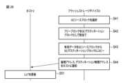
図28は、ガベージコレクション(GC)動作の手順を示す。Figure 28 shows the procedure for garbage collection (GC) operations.
フラッシュストレージデバイス3のコントローラ4は、ホスト2によって指定されたポリシーに基づいて、ソースQoSドメインIDによって指定されるQoSドメインに属するブロック群から、有効データと無効データとが混在する一つ以上のGCソースブロック(コピー元ブロック)を選択する(ステップS41)。次いで、コントローラ4は、デスティネーションQoSドメインIDによって指定されるQoSドメインに属するフリーブロック群から一つ以上のフリーブロックを選択し、選択したフリーブロックをGCデスティネーションブロック(コピー先ブロック)として割り当てる(ステップS42)。Based on the policy specified by the
コントローラ4は、GCソースブロック(コピー元ブロック)内の全ての有効データをGCデスティネーションブロック(コピー先ブロック)にコピーする(ステップS44)。ステップS44では、コントローラ4は、GCソースブロック(コピー元ブロック)内の有効データのみならず、この有効データとこの有効データに対応する論理アドレスの双方を、GCソースブロック(コピー元ブロック)からGCデスティネーションブロック(コピー先ブロック)にコピーする。これにより、GCデスティネーションブロック(コピー先ブロック)内にデータと論理アドレスとのペアを保持することができる。The
そして、コントローラ4は、コピーされた有効データの論理アドレスと、この有効データがコピーされたGCデスティネーションブロック(コピー先ブロック)内の位置を示すデスティネーション物理アドレス(ブロック番号、オフセット(ブロック内オフセット))を、GC用コールバックコマンドを使用してホスト2に通知する(ステップS44)。なお、ステップS44では、コントローラ4は、コピーされた有効データの論理アドレスとデスティネーション物理アドレスとみならず、ソース物理アドレスもホスト2に通知してもよい。Then, the
ホスト2がこのGC用コールバックコマンドを受信した時、ホスト2は、ホスト2によって管理されているLUTを更新して、コピーされた有効データに対応する論理アドレスそれぞれにデスティネーション物理アドレスをマッピングする(ステップS51)。When the
図29は、GCのために実行されるデータコピー動作の例を示す。Figure 29 shows an example of a data copy operation performed for GC.
図29では、GCソースブロック(ここではブロックBLK#50)のオフセット+4に対応する位置に格納されている有効データ(LBA=10)が、GCデスティネーションブロック(ここではブロックBLK#100)のオフセット+0に対応する位置にコピーされ、GCソースブロック(ここではブロックBLK#50)のオフセット+10に対応する位置に格納されている有効データ(LBA=20)が、GCデスティネーションブロック(ここではブロックBLK#100)のオフセット+1に対応する位置にコピーされた場合が想定されている。この場合、コントローラ4は、{LBA10、BLK#100、オフセット(=+0)、LBA20、BLK#100、オフセット(=+1)}をホストに通知する(GC用コールバック処理)。In FIG. 29, it is assumed that valid data (LBA=10) stored at a position corresponding to offset +4 in the GC source block (here, block BLK#50) is copied to a position corresponding to offset +0 in the GC destination block (here, block BLK#100), and valid data (LBA=20) stored at a position corresponding to offset +10 in the GC source block (here, block BLK#50) is copied to a position corresponding to offset +1 in the GC destination block (here, block BLK#100). In this case, the
図30は、図29のデータコピー動作の結果に基づいて更新されるホスト2のLUTの内容を示す。Figure 30 shows the contents of the LUT of
このLUTにおいては、LBA10に対応するブロック番号およびオフセットは、BLK#50、オフセット(=+4)から、BLK#100、オフセット(=+0)に更新される。同様に、LBA20に対応するブロック番号およびオフセットは、BLK#50、オフセット(=+10)から、BLK#100、オフセット(=+1)に更新される。In this LUT, the block number and offset corresponding to LBA10 are updated from
LUTが更新された後、ホスト2は、BLK#50およびオフセット(=+4)を指定するTrimコマンドをフラッシュストレージデバイス3に送信して、BLK#50のオフセット(=+4)に対応する位置に格納されているデータを無効化してもよい。さらに、ホスト2は、BLK#50およびオフセット(=+10)を指定するTrimコマンドをフラッシュストレージデバイス3に送信して、BLK#50のオフセット(=+10)に対応する位置に格納されているデータを無効化してもよい。After the LUT is updated, the
図31は、ライトコマンドに対するレスポンスとGC用コールバック処理との関係を示す。Figure 31 shows the relationship between the response to a write command and the GC callback process.
コントローラ4がある論理アドレスに対応する有効データをコピーしている間に、この論理アドレスを指定するライトコマンドがホスト2から受信されるというケースが起こる場合がある。There may be cases where a write command specifying a logical address is received from the
図31では、図29のデータコピー動作(LBA10に対応するデータコピー動作)の実行中に、LBA10を指定するライトコマンドがホスト2から受信された場合が想定されている。In FIG. 31, it is assumed that a write
コントローラ4は、ホスト2から受信されるライトデータを書き込み先ブロックに書き込む(ここではBLK#3のオフセット+0に対応する位置に書き込まれる)。そして、コントローラ4は、{LBA10、BLK#3、オフセット(=+0)}をホスト2に通知する。The
ホスト2は、LUTを更新して、LBA10に対応するブロック番号およびオフセットを、BLK#50、オフセット(+4)から、BLK#3、オフセット(+0)に変更する。
もしこの後に、LBA10のデスティネーション物理アドレスがコントローラ4からホスト2に通知されたならば、LBA10に対応する最新データが格納されている位置を示すブロック番号およびオフセット(BLK#3、オフセット(+0))が、LBA10に対応するデスティネーション物理アドレス(ここでは、BLK#100、オフセット(=+0))に誤って変更されてしまう可能性がある。If the destination physical address of LBA10 is subsequently notified to the
本実施形態では、コントローラ4は、LBA10とデスティネーション物理アドレス(BLK#100、オフセット(=+0))のみならず、ソース物理アドレス(BLK#50、オフセット(=+4))もホスト2に通知することができる。ホスト2は、ソース物理アドレス(BLK#50、オフセット(=+4))が、LUTによってLBA10に現在マッピングされているブロック番号、オフセットに一致しない場合には、LUTを更新しない。これにより、LBA10に対応する最新データが格納されている位置を示すブロック番号およびオフセット(BLK#3、オフセット(+0))が、LBA10に対応するデスティネーション物理アドレス(ここでは、BLK#100、オフセット(=+0))に誤って変更されてしまうことを防止することができる。In this embodiment, the
図32は、GC制御コマンドの別の例を示す。Figure 32 shows another example of a GC control command.
この図32のGC制御コマンドは、ソースQoSドメインIDの代わりに、ソースデバイスIDとソースQoSドメインIDのペアを指定してもよい。さらに、この図32のGC制御コマンドは、デスティネーションQoSドメインIDの代わりに、デスティネーションデバイスIDとデスティネーションQoSドメインIDのペアを指定してもよい。これにより、あるフラッシュストレージデバイス3をGCソースとして動作させ、別のフラッシュストレージデバイス3をGCデスティネーションとして動作させることが可能となる。ソースデバイスIDとデスティネーションデバイスIDが同じである場合には、一つのフラッシュストレージデバイス3内でGCが実行される。The GC control command in FIG. 32 may specify a pair of a source device ID and a source QoS domain ID instead of a source QoS domain ID. Furthermore, the GC control command in FIG. 32 may specify a pair of a destination device ID and a destination QoS domain ID instead of a destination QoS domain ID. This makes it possible to operate one
図33は、図32のGC制御コマンドに対応するGC用コールバックコマンドの例を示す。Figure 33 shows an example of a GC callback command corresponding to the GC control command in Figure 32.
図33のGC用コールバックコマンドは、デスティネーション物理アドレスの代わりに、デスティネーションデバイスIDとデスティネーション物理アドレスのペアを含む。また、図33のGC用コールバックコマンドは、ソース物理アドレス(オプショナル)の代わりに、ソースデバイスIDとソース物理アドレスのペア(オプショナル)を含んでもよい。The GC callback command in FIG. 33 includes a pair of a destination device ID and a destination physical address instead of a destination physical address. The GC callback command in FIG. 33 may also include a pair of a source device ID and a source physical address (optional) instead of a source physical address (optional).
いま、デバイスIDが1のフラッシュストレージデバイス3をGCソースとして動作させ、デバイスIDが2のフラッシュストレージデバイス3をGCデスティネーションとして動作させる場合を想定する。ホスト2は、ソースデバイスID#1およびデスティネーションデバイスID#2を指定するGC制御コマンドを、デバイスID#1のフラッシュストレージデバイス3と、デバイスID#2のフラッシュストレージデバイス3に送信してもよい。Now, assume that the
デバイスID#1のフラッシュストレージデバイス3は、ソースQoSドメインIDによって指定されるQoSドメインに属するブロック群からGCソースブロックを選択し、GCソースブロック内の有効データとこの有効データの論理アドレスとを、デスティネーションデバイスIDによって指定されるフラッシュストレージデバイス(デバイスID#2のフラッシュストレージデバイス)宛てに送信する。GCソースブロック内の有効データとこの有効データの論理アドレスは、例えば、図3のスイッチ1を介して、デバイスID#1のフラッシュストレージデバイス3からデバイスID#2のフラッシュストレージデバイス3に転送される。The
デバイスID#2のフラッシュストレージデバイス3は、デスティネーションQoSドメインIDによって指定されるQoSドメインに属するフリーブロック群からGCデスティネーションブロックを選択し、スイッチ1を介して受信される有効データおよび論理ドレスをGCデスティネーションブロックに書き込む(コピーする)。The
デバイスID#2のフラッシュストレージデバイス3は、コピーされた有効データの論理アドレスと、この有効データがコピーされたデスティネーション物理アドレス(ブロック番号、オフセット)を、GC用コールバックコマンドによってホスト2に通知する。The
デバイスID#1のフラッシュストレージデバイス3は、コピーされた有効データの論理アドレスと、この有効データが格納されているソース物理アドレス(ブロック番号、オフセット)を、GC用コールバックコマンドによってホスト2に通知する。The
図34は、書き込み/リード/GC動作を示す。Figure 34 shows the write/read/GC operations.
まず、ホスト2からのデータを書き込むホストライト動作について説明する。First, we will explain the host write operation, which writes data from
(1)コントローラ4は、ホスト2からLBAとライトデータを受信する。(1) The
(2)コントローラ4は、LBAとライトデータの双方を書き込み先ブロックに書き込む。書き込み先ブロックが割り当てられていない場合には、コントローラ4は、フリーブロックリストから一つのフリーブロックを選択し、この選択したフリーブロックを新たな書き込み先ブロックとして割り当てる。そして、コントローラ4は、LBAとライトデータの双方をこの新たな書き込み先ブロックに書き込む。(2) The
(3)コントローラ4は、このLBAと、このライトデータが書き込まれた書き込み先ブロック内の位置を示す物理アドレスPBAをホスト2に通知する。この物理アドレスPBAは、ブロック番号およびオフセットによって表される。書き込み先ブロック全体がデータで満たされると、コントローラ4は、この書き込み先ブロックをアクティブブロックリストに登録する。(3) The
次に、リード動作について説明する。Next, we will explain the read operation.
(4)ホスト2は、ホスト2によって管理されているLUTを参照して、ユーザアプリケーションからのリード要求に含まれるLBAをリード用物理アドレスPBA(ブロック番号、オフセット)に変換する。(4) The
(5)ホスト2から受信されるリード用物理アドレスPBA(ブロック番号、オフセット)に基づいて、コントローラ4は、このブロック番号を有するブロックをリード対象のブロックとして決定する。リード対象のブロックは、アクティブブロックリストによって管理されているブロック群(アクティブブロック)のいずれか一つ、または現在のGCソースブロック、または現在の書き込み先ブロックである。そして、コントローラ4は、オフセットに基づいて、リード対象のブロックからデータをリードする。(5) Based on the read physical address PBA (block number, offset) received from the
次に、GC動作について説明する。Next, we will explain GC operation.
(6)コントローラ4は、GCソースブロック(コピー元ブロック)およびGCデスティネーションブロック(コピー先ブロック)を選択し、GCソースブロック内に格納されている有効データとこの有効データのLBAの双方をGCデスティネーションブロックにコピーする。(6) The
(7)コントローラ4は、コピーされた有効データのLBAと、この有効データがコピーされたGCデスティネーションブロック内の位置を示すPBA(ブロック番号、オフセット)の双方を、ホスト2に通知する。(7) The
あるいは、コントローラ4は、コピーされた有効データのLBAと、この有効データがコピーされたGCデスティネーションブロック内の位置を示すPBA(ブロック番号、オフセット)と、この有効データが格納されているGCソースブロック内の位置を示すPBA(ブロック番号、オフセット)とを、ホスト2に通知してもよい。Alternatively, the
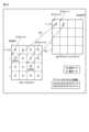
図35は、参照カウントを管理するためのブロック管理テーブルの構成例を示す。Figure 35 shows an example of the configuration of a block management table for managing reference counts.
ホスト2は重複排除機能をサポートしている。したがって、ユーザアプリケーションから書き込み要求されたデータと一致する重複データがフラッシュストレージデバイス3(NAND型フラッシュメモリ5)にすでに存在する場合には、ホスト2は、このデータをフラッシュストレージデバイス3に書き込まず、このデータが格納されている位置(ブロック番号、オフセット)を指すポインタのみを、書き込み要求されたデータのLBAに関連付ける。このため、フラッシュストレージデバイス3(NAND型フラッシュメモリ5)に格納されている各4Kバイトデータは、一つの論理アドレスから参照されるだけでなく、複数の論理アドレスから参照される可能性がある。The
本実施形態においては、フラッシュストレージデバイス3は、4Kバイトデータ毎に参照カウントを管理する機能を有している。ここで、あるデータに対応する参照カウントは、このデータを参照している論理アドレスの数を示す。In this embodiment, the
図35では、ブロックBLK#1用のブロック管理テーブルが例示されている。Figure 35 shows an example of a block management table for
ブロックBLK#1用のブロック管理テーブルは、ブロックBLK#1の複数のオフセット値それぞれに対応する複数のエントリを含む。The block management table for
例えば、オフセット+0に対応するエントリには、ブロックBLK#1のオフセット+0に対応する位置に格納されている4KBデータに対応する参照カウントが格納される。同様に、オフセット+1に対応するエントリには、ブロックBLK#1のオフセット+1に対応する位置に格納されている4KBデータに対応する参照カウントが格納される。For example, the entry corresponding to offset +0 stores a reference count corresponding to 4 KB data stored at a position corresponding to offset +0 in
参照カウントが1以上であるデータは有効データであり、参照カウントが0のデータは無効データである。Data with a reference count of 1 or greater is valid data, and data with a reference count of 0 is invalid data.
フラッシュストレージデバイス3は、ホスト2から受信されるデュプリケートコマンド/Ttimコマンドに基づいて、参照カウントをインクリメント/デクリメントする。The
図36は、参照カウントの管理のためにフラッシュストレージデバイス3に適用されるデュプリケートコマンドを示す。Figure 36 shows the duplicate command applied to
デュプリケートコマンドは、ある物理アドレス(ブロック番号、オフセット)に格納されているデータの参照カウントを1増やすことをフラッシュストレージデバイス3に要求するコマンドである。The duplicate command is a command that requests the
このデュプリケートコマンドは、コマンドID、物理アドレスPBA、長さ、等を含んでもよい。This duplicate command may include a command ID, a physical address PBA, a length, etc.
コマンドIDはこのコマンドがデュプリケートコマンドであることを示すID(コマンドコード)であり、デュプリケートコマンドにはデュプリケートコマンド用のコマンドIDが含まれる。The command ID is an ID (command code) that indicates that this command is a duplicate command, and the duplicate command contains a command ID for the duplicate command.
物理アドレスPBAは、参照カウントを1だけ増やすべきデータが格納されている最初の物理記憶位置を示す。物理アドレスPBAは、ブロック番号、オフセット(ブロック内オフセット)によって指定される。The physical address PBA indicates the first physical memory location where the data for which the reference count should be increased by 1 is stored. The physical address PBA is specified by the block number and offset (offset within the block).
長さは、参照カウントを1だけ増やすべきデータの長さを示す。このデータ長は、粒度(Grain)の数によって指定可能である。The length indicates the length of the data for which the reference count should be increased by 1. This data length can be specified by the number of grains.
コントローラ4は、参照カウントを増やすべきデータが格納されている物理記憶位置を示すブロック番号およびブロック内オフセットを含むデュプリケートコマンドをホスト2から受信した場合、ブロック管理テーブル32を更新して、デュプリケートコマンドに含まれるブロック番号およびブロック内オフセットに対応する物理記憶位置のデータに対応する参照カウントを1増やす。When the
図37は、参照カウントの管理のためにフラッシュストレージデバイス3に適用されるTrimコマンドを示す。Figure 37 shows the Trim command applied to the
このTrimコマンドは、ある物理アドレス(ブロック番号、オフセット)に格納されているデータの参照カウントを1減らすことをフラッシュストレージデバイス3に要求するコマンドである。This Trim command requests the
このTrimコマンドは、コマンドID、物理アドレスPBA、長さ、等を含んでもよい。This Trim command may include a command ID, a physical address PBA, a length, etc.
コマンドIDはこのコマンドがTrimコマンドであることを示すID(コマンドコード)であり、TrimコマンドにはTrimコマンド用のコマンドIDが含まれる。The command ID is an ID (command code) that indicates that this command is a Trim command, and the Trim command includes a command ID for the Trim command.
物理アドレスPBAは、参照カウントを1だけ減らすべきデータが格納されている最初の物理記憶位置を示す。物理アドレスPBAは、ブロック番号、オフセット(ブロック内オフセット)によって指定される。The physical address PBA indicates the first physical memory location where the data whose reference count is to be decremented by 1 is stored. The physical address PBA is specified by the block number and offset (offset within the block).
長さは、参照カウントを1だけ減らすべきデータの長さを示す。このデータ長は、粒度(Grain)の数によって指定可能である。The length indicates the length of the data for which the reference count should be decremented by 1. This data length can be specified by the number of grains.
コントローラ4は、参照カウントを減らすべきデータが格納されている物理記憶位置を示すブロック番号およびブロック内オフセットを含むTrimコマンドをホスト2から受信した場合、ブロック管理テーブル32を更新して、Trimコマンドに含まれるブロック番号およびブロック内オフセットに対応する物理記憶位置のデータに対応する参照カウントを1減らす。When the
図38は、参照カウントインクリメント/デクリメント処理を示す。Figure 38 shows the reference count increment/decrement process.
フラッシュストレージデバイス3のコントローラ4がホスト2からデュプリケートコマンドを受信した時、コントローラ4は、デュプリケートコマンドによって指定される物理アドレスPBA(ブロック番号、オフセット)に対応する参照カウント、つまり、このブロック番号およびオフセットによって指定されるNAND型フラッシュメモリ5内の物理記憶位置に格納されているデータに対応する参照カウントを1増やす(ステップS61)。この場合、コントローラ4は、デュプリケートコマンドによって指定されるブロック番号を有するブロックに対応するブロック管理テーブル32を更新する。このブロック管理テーブル32の更新では、デュプリケートコマンドによって指定されるオフセットに対応するブロック管理テーブル32内のエントリに格納されている参照カウントが1増やされる。デュプリケートコマンドによって指定される長さが2以上の場合には、デュプリケートコマンドによって指定されるオフセットに対応する参照カウントのみならず、このオフセットに後続する幾つかのオフセットに対応する参照カウントも1増やされる。When the
フラッシュストレージデバイス3のコントローラ4がホスト2からTrimコマンドを受信した時、コントローラ4は、Trimコマンドによって指定される物理アドレスPBA(ブロック番号、オフセット)に対応する参照カウント、つまり、このブロック番号およびオフセットによって指定されるNAND型フラッシュメモリ5内の物理記憶位置に格納されているデータに対応する参照カウントを1減らす(ステップS62)。この場合、コントローラ4は、Trimコマンドによって指定されるブロック番号を有するブロックに対応するブロック管理テーブル32を更新する。このブロック管理テーブル32の更新では、Trimコマンドによって指定されるオフセットに対応するブロック管理テーブル32内のエントリに格納されている参照カウントが1減らされる。Trimコマンドによって指定される長さが2以上の場合には、Trimコマンドによって指定されるオフセットに対応する参照カウントのみならず、このオフセットに後続する幾つかのオフセットに対応する参照カウントも1減らされる。When the
GCにおいては、コントローラ4は、GCソースブロックに対応するブロック管理テーブルを参照して、サイズが4KBであるデータ単位で、GCソースブロック内のデータが有効データであるか無効データであるかを判定する。コントローラ4は、参照カウントが0であるデータは無効データであると判定し、参照カウントが1以上であるデータは有効データであると判定する。そして、コントローラ4は、有効データ(参照カウントが1以上のデータ)とこの有効データに対応する論理アドレスをGCソースブロックからGCデスティネーションブロックにコピーする。In GC, the
より詳しくは、コントローラ4は、NAND型フラッシュメモリ5のガベージコレクションを実行する場合、ガベージコレクションのためのコピー元ブロックおよびコピー先ブロックを選択する。コントローラ4は、コピー元ブロック内に格納されている、参照カウントが1以上の第1のデータ(有効データ)と第1のデータの論理アドレスの双方をコピー先ブロックにコピーする。そして、コントローラ4は、第1のデータの論理アドレスと、コピー先ブロックのブロック番号と、第1のデータがコピーされた、コピー先ブロックの先頭からのオフセット位置を粒度の倍数で示すブロック内オフセットとを、ホスト2に通知する。More specifically, when the
以上説明したように、本実施形態によれば、ホスト2ではなく、フラッシュストレージデバイス3が、ホスト2からのデータ(ユーザデータ)を書き込むべき書き込み先ブロックおよびこの書き込み先ブロック内の位置(書き込み先位置)を決定する。フラッシュストレージデバイス3は、ユーザデータを書き込み先ブロック内の書き込み先位置に書き込み、そして、書き込み先ブロックのブロック番号と、書き込み先ブロックの先頭から書き込み先位置までのオフセットをページサイズとは異なるサイズを有する粒度の倍数で示すブロック内オフセットとをホスト2に通知する。これにより、ホスト2は、ブロックサイズ、ページ書き込み順序制約、バッドページ、ページサイズ等を意識を意識することなく、ユーザデータをNAND型フラッシュメモリ5に書き込むことができ、さらに、ブロック番号およびブロック内オフセットによって表される物理アドレス(抽象化された物理アドレス)をこのユーザデータの論理アドレスにマッピングすることができる。As described above, according to this embodiment, the
このように、フラッシュストレージデバイス3が、書き込み先ブロックおよびこの書き込み先ブロック内の位置を決定し、且つブロック番号とブロック内オフセットとをホスト2に返すという構成により、上位階層(ホスト2)のアプリケーションレベルアドレス変換テーブルと従来型SSDのLUTレベルアドレス変換テーブルとのマージを実現することが可能となり、しかも、フラッシュストレージデバイス3が、NAND型フラッシュメモリ5の特徴/制約を考慮してNAND型フラッシュメモリ5を制御することが可能となる。したがって、ホスト2とフラッシュストレージデバイス3との間の適切な役割分担を実現でき、これによってホスト2とフラッシュストレージデバイス3とを含むシステム全体のI/O性能の向上を図ることができる。In this way, the
また、本実施形態によれば、アドレス変換テーブルを管理するホスト2ではなく、フラッシュストレージデバイス3がガベージコレクションのためのコピー元ブロックおよびコピー先ブロックを選択し、コピー元ブロック内に格納されている有効データをコピー先ブロックにコピーする。そして、フラッシュストレージデバイス3が、コピーされた有効データの論理アドレスと、コピー先ブロックのブロック番号と、有効データがコピーされたコピー先ブロック内の位置を示すブロック内オフセットとを、ホスト2に通知する。このように、ガベージコレクションはフラッシュストレージデバイス3によって実行され、しかも論理アドレス、ブロック番号、ブロック内オフセットがフラッシュストレージデバイス3からホスト2に通知されるので、ホスト2は、論理アドレスそれぞれとNAND型フラッシュメモリ5の物理アドレス(つまり、ブロック番号とブロック内オフセットとのペア)それぞれとの間のマッピングをアドレス変換テーブル(LUT)を使用して正しい管理することができる。また、アプリケーションレベルGCをフラッシュストレージデバイス3のGCとマージすることができので、ライトアンプリフィケーションを大幅に低減することができる。According to this embodiment, the
なお、フラッシュストレージデバイス3は、ストレージアレイ内に設けられる複数のフラッシュストレージデバイス3の一つとして利用されてもよい。ストレージアレイは、サーバ計算機のような情報処理装置にケーブルまたはネットワークを介して接続されてもよい。ストレージアレイは、このストレージアレイ内の複数のフラッシュストレージデバイス3を制御するコントローラを含む。フラッシュストレージデバイス3がストレージアレイに適用された場合には、このストレージアレイのコントローラが、フラッシュストレージデバイス3のホスト2として機能してもよい。The
また、本実施形態では、不揮発性メモリとしてNAND型フラッシュメモリを例示した。しかし、本実施形態の機能は、例えば、MRAM(Magnetoresistive
Random Access Memory)、PRAM(Phase change
Random Access Memory)、ReRAM(Resistive Random Access Memory)、又は、FeRAM(Ferroelectric Random Access Memory)のような他の様々な不揮発性メモリにも適用できる。 In the present embodiment, a NAND flash memory is exemplified as a nonvolatile memory. However, the function of the present embodiment can be applied to, for example, an MRAM (Magnetoresistive Random Access Memory).
Random Access Memory), PRAM (Phase change
The present invention can also be applied to various other non-volatile memories such as Random Access Memory (RRAM), Resistive Random Access Memory (ReRAM), or Ferroelectric Random Access Memory (FeRAM).
本発明のいくつかの実施形態を説明したが、これらの実施形態は、例として提示したものであり、発明の範囲を限定することは意図していない。これら新規な実施形態は、その他の様々な形態で実施されることが可能であり、発明の要旨を逸脱しない範囲で、種々の省略、置き換え、変更を行うことができる。これら実施形態やその変形は、発明の範囲や要旨に含まれるとともに、特許請求の範囲に記載された発明とその均等の範囲に含まれる。Although several embodiments of the present invention have been described, these embodiments are presented as examples and are not intended to limit the scope of the invention. These novel embodiments can be implemented in various other forms, and various omissions, substitutions, and modifications can be made without departing from the gist of the invention. These embodiments and their modifications are included in the scope and gist of the invention, and are included in the scope of the invention and its equivalents described in the claims.
2…ホスト、3…フラッシュストレージデバイス、4…コントローラ、5…NAND型フラッシュメモリ、21…ライト動作制御部、22…リード動作制御部、23…GC動作制御部。2... host, 3... flash storage device, 4... controller, 5... NAND flash memory, 21... write operation control unit, 22... read operation control unit, 23... GC operation control unit.
Claims (18)
Translated fromJapanese各々が消去動作の単位である複数のブロックを各々が有する複数のメモリダイを含む不揮発性メモリと、
前記不揮発性メモリに電気的に接続されたコントローラとを具備し、
前記コントローラは、
前記複数のメモリダイの各々が一つのドメインのみに属するように前記複数のメモリダイを複数のドメインに分類し、
第1のデータの書き込みを要求し且つ前記第1のデータが書き込まれるべきドメインの識別子を少なくとも指定するライトコマンドを前記ホストから受信した場合、前記複数のドメインから、前記指定された識別子に関連付けられたドメインを選択し、前記選択されたドメインに属する第1のメモリダイに含まれるブロックの集合から、前記第1のデータが書き込まれるべき第1のブロックを選択し、前記第1のデータを前記第1のブロック内の第1の記憶位置に書き込み、
少なくとも前記第1のメモリダイの識別子と前記第1のブロックの識別子とを用いて前記第1の記憶位置を前記ホストに通知するように構成されている、メモリシステム。 1. A memory system connectable to a host, comprising:
A non-volatile memory including a plurality of memory dies each having a plurality of blocks each being a unit of an erase operation;
a controller electrically connected to the non-volatile memory;
The controller:
classifying the plurality of memory dies into a plurality of domains such that each of the plurality of memory dies belongs to only one domain;
when a write command is received from the host requesting writing of first data and specifying at least an identifier of a domain to which the first data is to be written, selecting a domain associated with the specified identifier from among the plurality of domains, selecting a first block to which the first data is to be written from a set of blocks included in a first memory die belonging to the selected domain, and writing the first data to a first memory location within the first block;
11. A memory system configured to inform the hostof the first storage location using at least an identifier of the first memory die and an identifier of the first block.
前記コントローラは、前記複数のページの各々のサイズとは異なるサイズを有する粒度の倍数を使用して前記オフセットアドレスを指定する、請求項3記載のメモリシステム。 Each of the plurality of blocks includes a plurality of pages, and each of the plurality of pages is a unit of a data write operation;
4. The memory system of claim 3, wherein the controller specifies the offset address using a multiple of a granularity having a size different from a size of each of the plurality of pages.
前記第1のデータと前記論理アドレスを前記第1のブロックから前記不揮発性メモリの第2のブロック内の第2の記憶位置にコピーし、
前記第2の記憶位置と前記論理アドレスとを前記ホストに通知するようにさらに構成されている、請求項7記載のメモリシステム。 The controller:
copying the first data and the logical address from the first block to a second location in a second block of the non-volatile memory;
8. The memory system of claim 7, further configured to communicate said second storage location and said logical address to said host.
前記複数のメモリダイの各々が一つのドメインのみに属するように前記複数のメモリダイを複数のドメインに分類することと、
第1のデータの書き込みを要求し且つ前記第1のデータが書き込まれるべきドメインの識別子を少なくとも指定するライトコマンドをホストから受信した場合、前記複数のドメインから、前記指定された識別子に関連付けられたドメインを選択し、前記選択されたドメインに属する第1のメモリダイに含まれるブロックの集合から、前記第1のデータが書き込まれるべき第1のブロックを選択し、前記第1のデータを前記第1のブロック内の第1の記憶位置に書き込むことと、
少なくとも前記第1のメモリダイの識別子と前記第1のブロックの識別子とを用いて前記第1の記憶位置を前記ホストに通知することとを具備する、制御方法。 A method for controlling a non-volatile memory including a plurality of memory dies, each of which has a plurality of blocks that are units of an erase operation, by a controller, comprising:
classifying the plurality of memory dies into a plurality of domains such that each of the plurality of memory dies belongs to only one domain;
when receiving a write command from a host requesting writing of first data and specifying at least an identifier of a domain to which the first data is to be written, selecting a domain associated with the specified identifier from among the multiple domains, selecting a first block to which the first data is to be written from a set of blocks included in a first memory die belonging to the selected domain, and writing the first data to a first memory location in the first block;
and informing the hostof the first memory location using at least an identifier of the first memory die and an identifier of the first block.
前記オフセットアドレスは、前記複数のページの各々のサイズとは異なるサイズを有する粒度の倍数を使用して指定される、請求項12記載の制御方法。 Each of the plurality of blocks includes a plurality of pages, and each of the plurality of pages is a unit of a data write operation;
The control method according to claim 12 , wherein the offset address is specified using a multiple of a granularity having a size different from a size of each of the plurality of pages.
前記第2の記憶位置と前記論理アドレスとを前記ホストに通知することとをさらに具備する、請求項16記載の制御方法。 copying the first data and the logical address from the first block to a second storage location in a second block of the non-volatile memory;
17. The method of claim 16, further comprising: notifying the host of the second storage location and the logical address.
Priority Applications (1)
| Application Number | Priority Date | Filing Date | Title |
|---|---|---|---|
| JP2023180929AJP7524443B2 (en) | 2020-10-23 | 2023-10-20 | MEMORY SYSTEM AND CONTROL METHOD - Patent application |
Applications Claiming Priority (3)
| Application Number | Priority Date | Filing Date | Title |
|---|---|---|---|
| JP2020177990AJP7102482B2 (en) | 2020-10-23 | 2020-10-23 | Memory system and control method |
| JP2022106944AJP7490714B2 (en) | 2020-10-23 | 2022-07-01 | MEMORY SYSTEM AND CONTROL METHOD - Patent application |
| JP2023180929AJP7524443B2 (en) | 2020-10-23 | 2023-10-20 | MEMORY SYSTEM AND CONTROL METHOD - Patent application |
Related Parent Applications (1)
| Application Number | Title | Priority Date | Filing Date |
|---|---|---|---|
| JP2022106944ADivisionJP7490714B2 (en) | 2020-10-23 | 2022-07-01 | MEMORY SYSTEM AND CONTROL METHOD - Patent application |
Publications (2)
| Publication Number | Publication Date |
|---|---|
| JP2023174933A JP2023174933A (en) | 2023-12-08 |
| JP7524443B2true JP7524443B2 (en) | 2024-07-29 |
Family
ID=74165291
Family Applications (3)
| Application Number | Title | Priority Date | Filing Date |
|---|---|---|---|
| JP2020177990AActiveJP7102482B2 (en) | 2020-10-23 | 2020-10-23 | Memory system and control method |
| JP2022106944AActiveJP7490714B2 (en) | 2020-10-23 | 2022-07-01 | MEMORY SYSTEM AND CONTROL METHOD - Patent application |
| JP2023180929AActiveJP7524443B2 (en) | 2020-10-23 | 2023-10-20 | MEMORY SYSTEM AND CONTROL METHOD - Patent application |
Family Applications Before (2)
| Application Number | Title | Priority Date | Filing Date |
|---|---|---|---|
| JP2020177990AActiveJP7102482B2 (en) | 2020-10-23 | 2020-10-23 | Memory system and control method |
| JP2022106944AActiveJP7490714B2 (en) | 2020-10-23 | 2022-07-01 | MEMORY SYSTEM AND CONTROL METHOD - Patent application |
Country Status (1)
| Country | Link |
|---|---|
| JP (3) | JP7102482B2 (en) |
Families Citing this family (1)
| Publication number | Priority date | Publication date | Assignee | Title |
|---|---|---|---|---|
| KR20250118679A (en)* | 2024-01-30 | 2025-08-06 | 삼성전자주식회사 | Non-volatile memory and storage device including the same |
Citations (6)
| Publication number | Priority date | Publication date | Assignee | Title |
|---|---|---|---|---|
| WO2011068109A1 (en) | 2009-12-03 | 2011-06-09 | 株式会社日立製作所 | Storage device and memory controller |
| JP2011253250A (en) | 2010-05-31 | 2011-12-15 | Toshiba Corp | Data storage device and memory adjustment method |
| JP2013097789A (en) | 2011-10-31 | 2013-05-20 | Apple Inc | Systems and methods for obtaining and using nonvolatile memory health information |
| WO2016013076A1 (en) | 2014-07-23 | 2016-01-28 | 富士通株式会社 | Information processing device, memory controller, storage device control program, and storage device control method |
| JP2017027387A (en) | 2015-07-23 | 2017-02-02 | 株式会社東芝 | Memory system |
| JP2017162068A (en) | 2016-03-08 | 2017-09-14 | 東芝メモリ株式会社 | Storage system, information processing system, and control method |
Family Cites Families (5)
| Publication number | Priority date | Publication date | Assignee | Title |
|---|---|---|---|---|
| US8285946B2 (en)* | 2009-12-15 | 2012-10-09 | International Business Machines Corporation | Reducing access contention in flash-based memory systems |
| JP5093294B2 (en)* | 2010-05-14 | 2012-12-12 | Tdk株式会社 | MEMORY CONTROLLER, FLASH MEMORY SYSTEM HAVING MEMORY CONTROLLER, AND FLASH MEMORY CONTROL METHOD |
| US20160321010A1 (en)* | 2015-04-28 | 2016-11-03 | Kabushiki Kaisha Toshiba | Storage system having a host directly manage physical data locations of storage device |
| JP2017027388A (en)* | 2015-07-23 | 2017-02-02 | 株式会社東芝 | Memory system and control method for nonvolatile memory |
| JP6523193B2 (en)* | 2016-03-08 | 2019-05-29 | 東芝メモリ株式会社 | Storage system, information processing system and control method |
- 2020
- 2020-10-23JPJP2020177990Apatent/JP7102482B2/enactiveActive
- 2022
- 2022-07-01JPJP2022106944Apatent/JP7490714B2/enactiveActive
- 2023
- 2023-10-20JPJP2023180929Apatent/JP7524443B2/enactiveActive
Patent Citations (6)
| Publication number | Priority date | Publication date | Assignee | Title |
|---|---|---|---|---|
| WO2011068109A1 (en) | 2009-12-03 | 2011-06-09 | 株式会社日立製作所 | Storage device and memory controller |
| JP2011253250A (en) | 2010-05-31 | 2011-12-15 | Toshiba Corp | Data storage device and memory adjustment method |
| JP2013097789A (en) | 2011-10-31 | 2013-05-20 | Apple Inc | Systems and methods for obtaining and using nonvolatile memory health information |
| WO2016013076A1 (en) | 2014-07-23 | 2016-01-28 | 富士通株式会社 | Information processing device, memory controller, storage device control program, and storage device control method |
| JP2017027387A (en) | 2015-07-23 | 2017-02-02 | 株式会社東芝 | Memory system |
| JP2017162068A (en) | 2016-03-08 | 2017-09-14 | 東芝メモリ株式会社 | Storage system, information processing system, and control method |
Also Published As
| Publication number | Publication date |
|---|---|
| JP2023174933A (en) | 2023-12-08 |
| JP7102482B2 (en) | 2022-07-19 |
| JP2022121655A (en) | 2022-08-19 |
| JP2021007058A (en) | 2021-01-21 |
| JP7490714B2 (en) | 2024-05-27 |
Similar Documents
| Publication | Publication Date | Title |
|---|---|---|
| US12038834B2 (en) | Memory system and method for controlling nonvolatile memory during command processing without replacing defective blocks | |
| US11669444B2 (en) | Computing system and method for controlling storage device | |
| JP6785205B2 (en) | Memory system and control method | |
| US11797436B2 (en) | Memory system and method for controlling nonvolatile memory | |
| JP6982468B2 (en) | Memory system and control method | |
| JP7013546B2 (en) | Memory system | |
| JP7524443B2 (en) | MEMORY SYSTEM AND CONTROL METHOD - Patent application | |
| JP7661297B2 (en) | Memory System | |
| JP7567009B2 (en) | MEMORY SYSTEM AND CONTROL METHOD - Patent application | |
| JP7204020B2 (en) | Control method | |
| JP7167295B2 (en) | Memory system and control method |
Legal Events
| Date | Code | Title | Description |
|---|---|---|---|
| A621 | Written request for application examination | Free format text:JAPANESE INTERMEDIATE CODE: A621 Effective date:20231020 | |
| A521 | Request for written amendment filed | Free format text:JAPANESE INTERMEDIATE CODE: A523 Effective date:20231109 | |
| A977 | Report on retrieval | Free format text:JAPANESE INTERMEDIATE CODE: A971007 Effective date:20240410 | |
| A131 | Notification of reasons for refusal | Free format text:JAPANESE INTERMEDIATE CODE: A131 Effective date:20240416 | |
| A521 | Request for written amendment filed | Free format text:JAPANESE INTERMEDIATE CODE: A523 Effective date:20240425 | |
| TRDD | Decision of grant or rejection written | ||
| A01 | Written decision to grant a patent or to grant a registration (utility model) | Free format text:JAPANESE INTERMEDIATE CODE: A01 Effective date:20240618 | |
| A61 | First payment of annual fees (during grant procedure) | Free format text:JAPANESE INTERMEDIATE CODE: A61 Effective date:20240717 | |
| R150 | Certificate of patent or registration of utility model | Ref document number:7524443 Country of ref document:JP Free format text:JAPANESE INTERMEDIATE CODE: R150 |