JP7519507B2 - Plasma processing apparatus and plasma processing method - Google Patents
Plasma processing apparatus and plasma processing methodDownload PDFInfo
- Publication number
- JP7519507B2 JP7519507B2JP2023097775AJP2023097775AJP7519507B2JP 7519507 B2JP7519507 B2JP 7519507B2JP 2023097775 AJP2023097775 AJP 2023097775AJP 2023097775 AJP2023097775 AJP 2023097775AJP 7519507 B2JP7519507 B2JP 7519507B2
- Authority
- JP
- Japan
- Prior art keywords
- period
- frequency power
- lower electrode
- high frequency
- plasma processing
- Prior art date
- Legal status (The legal status is an assumption and is not a legal conclusion. Google has not performed a legal analysis and makes no representation as to the accuracy of the status listed.)
- Active
Links
- 238000003672processing methodMethods0.000titleclaimsdescription22
- 239000000758substrateSubstances0.000claimsdescription70
- 238000000034methodMethods0.000description13
- 150000002500ionsChemical class0.000description12
- XAGFODPZIPBFFR-UHFFFAOYSA-NaluminiumChemical compound[Al]XAGFODPZIPBFFR-UHFFFAOYSA-N0.000description5
- 229910052782aluminiumInorganic materials0.000description5
- 239000000919ceramicSubstances0.000description3
- 238000010586diagramMethods0.000description3
- 238000009792diffusion processMethods0.000description3
- SIWVEOZUMHYXCS-UHFFFAOYSA-Noxo(oxoyttriooxy)yttriumChemical compoundO=[Y]O[Y]=OSIWVEOZUMHYXCS-UHFFFAOYSA-N0.000description3
- 239000010453quartzSubstances0.000description3
- VYPSYNLAJGMNEJ-UHFFFAOYSA-Nsilicon dioxideInorganic materialsO=[Si]=OVYPSYNLAJGMNEJ-UHFFFAOYSA-N0.000description3
- 239000013626chemical specieSubstances0.000description2
- 239000004020conductorSubstances0.000description2
- 239000003989dielectric materialSubstances0.000description2
- 238000012986modificationMethods0.000description2
- 230000004048modificationEffects0.000description2
- 239000003507refrigerantSubstances0.000description2
- 229910052710siliconInorganic materials0.000description2
- 239000010703siliconSubstances0.000description2
- 238000007792additionMethods0.000description1
- 238000002048anodisation reactionMethods0.000description1
- 238000007743anodisingMethods0.000description1
- 239000011248coating agentSubstances0.000description1
- 238000000576coating methodMethods0.000description1
- PMHQVHHXPFUNSP-UHFFFAOYSA-Mcopper(1+);methylsulfanylmethane;bromideChemical compoundBr[Cu].CSCPMHQVHHXPFUNSP-UHFFFAOYSA-M0.000description1
- 230000007423decreaseEffects0.000description1
- 230000003111delayed effectEffects0.000description1
- 230000005684electric fieldEffects0.000description1
- 238000009616inductively coupled plasmaMethods0.000description1
- 239000011810insulating materialSubstances0.000description1
- 239000012212insulatorSubstances0.000description1
- 239000007788liquidSubstances0.000description1
- TWNQGVIAIRXVLR-UHFFFAOYSA-Noxo(oxoalumanyloxy)alumaneChemical compoundO=[Al]O[Al]=OTWNQGVIAIRXVLR-UHFFFAOYSA-N0.000description1
- HBMJWWWQQXIZIP-UHFFFAOYSA-Nsilicon carbideChemical compound[Si+]#[C-]HBMJWWWQQXIZIP-UHFFFAOYSA-N0.000description1
- 229910010271silicon carbideInorganic materials0.000description1
- 238000006467substitution reactionMethods0.000description1
- 230000001360synchronised effectEffects0.000description1
- 230000008016vaporizationEffects0.000description1
Images


Classifications
- H—ELECTRICITY
- H01—ELECTRIC ELEMENTS
- H01J—ELECTRIC DISCHARGE TUBES OR DISCHARGE LAMPS
- H01J37/00—Discharge tubes with provision for introducing objects or material to be exposed to the discharge, e.g. for the purpose of examination or processing thereof
- H01J37/32—Gas-filled discharge tubes
- H01J37/32009—Arrangements for generation of plasma specially adapted for examination or treatment of objects, e.g. plasma sources
- H01J37/32082—Radio frequency generated discharge
- H01J37/32137—Radio frequency generated discharge controlling of the discharge by modulation of energy
- H—ELECTRICITY
- H01—ELECTRIC ELEMENTS
- H01J—ELECTRIC DISCHARGE TUBES OR DISCHARGE LAMPS
- H01J37/00—Discharge tubes with provision for introducing objects or material to be exposed to the discharge, e.g. for the purpose of examination or processing thereof
- H01J37/32—Gas-filled discharge tubes
- H01J37/32009—Arrangements for generation of plasma specially adapted for examination or treatment of objects, e.g. plasma sources
- H01J37/32082—Radio frequency generated discharge
- H01J37/32091—Radio frequency generated discharge the radio frequency energy being capacitively coupled to the plasma
- H—ELECTRICITY
- H01—ELECTRIC ELEMENTS
- H01J—ELECTRIC DISCHARGE TUBES OR DISCHARGE LAMPS
- H01J37/00—Discharge tubes with provision for introducing objects or material to be exposed to the discharge, e.g. for the purpose of examination or processing thereof
- H01J37/32—Gas-filled discharge tubes
- H01J37/32009—Arrangements for generation of plasma specially adapted for examination or treatment of objects, e.g. plasma sources
- H01J37/32082—Radio frequency generated discharge
- H01J37/32137—Radio frequency generated discharge controlling of the discharge by modulation of energy
- H01J37/32146—Amplitude modulation, includes pulsing
- H—ELECTRICITY
- H01—ELECTRIC ELEMENTS
- H01J—ELECTRIC DISCHARGE TUBES OR DISCHARGE LAMPS
- H01J37/00—Discharge tubes with provision for introducing objects or material to be exposed to the discharge, e.g. for the purpose of examination or processing thereof
- H01J37/32—Gas-filled discharge tubes
- H01J37/32009—Arrangements for generation of plasma specially adapted for examination or treatment of objects, e.g. plasma sources
- H01J37/32082—Radio frequency generated discharge
- H01J37/32174—Circuits specially adapted for controlling the RF discharge
- H—ELECTRICITY
- H01—ELECTRIC ELEMENTS
- H01J—ELECTRIC DISCHARGE TUBES OR DISCHARGE LAMPS
- H01J37/00—Discharge tubes with provision for introducing objects or material to be exposed to the discharge, e.g. for the purpose of examination or processing thereof
- H01J37/32—Gas-filled discharge tubes
- H01J37/32431—Constructional details of the reactor
- H01J37/32532—Electrodes
- H—ELECTRICITY
- H01—ELECTRIC ELEMENTS
- H01L—SEMICONDUCTOR DEVICES NOT COVERED BY CLASS H10
- H01L21/00—Processes or apparatus adapted for the manufacture or treatment of semiconductor or solid state devices or of parts thereof
- H01L21/02—Manufacture or treatment of semiconductor devices or of parts thereof
- H01L21/04—Manufacture or treatment of semiconductor devices or of parts thereof the devices having potential barriers, e.g. a PN junction, depletion layer or carrier concentration layer
- H01L21/18—Manufacture or treatment of semiconductor devices or of parts thereof the devices having potential barriers, e.g. a PN junction, depletion layer or carrier concentration layer the devices having semiconductor bodies comprising elements of Group IV of the Periodic Table or AIIIBV compounds with or without impurities, e.g. doping materials
- H01L21/30—Treatment of semiconductor bodies using processes or apparatus not provided for in groups H01L21/20 - H01L21/26
- H01L21/302—Treatment of semiconductor bodies using processes or apparatus not provided for in groups H01L21/20 - H01L21/26 to change their surface-physical characteristics or shape, e.g. etching, polishing, cutting
- H01L21/306—Chemical or electrical treatment, e.g. electrolytic etching
- H01L21/3065—Plasma etching; Reactive-ion etching
- H—ELECTRICITY
- H05—ELECTRIC TECHNIQUES NOT OTHERWISE PROVIDED FOR
- H05H—PLASMA TECHNIQUE; PRODUCTION OF ACCELERATED ELECTRICALLY-CHARGED PARTICLES OR OF NEUTRONS; PRODUCTION OR ACCELERATION OF NEUTRAL MOLECULAR OR ATOMIC BEAMS
- H05H1/00—Generating plasma; Handling plasma
- H05H1/24—Generating plasma
- H05H1/46—Generating plasma using applied electromagnetic fields, e.g. high frequency or microwave energy
- H05H1/4645—Radiofrequency discharges
- H—ELECTRICITY
- H01—ELECTRIC ELEMENTS
- H01J—ELECTRIC DISCHARGE TUBES OR DISCHARGE LAMPS
- H01J37/00—Discharge tubes with provision for introducing objects or material to be exposed to the discharge, e.g. for the purpose of examination or processing thereof
- H01J37/32—Gas-filled discharge tubes
- H01J37/32431—Constructional details of the reactor
- H01J37/32715—Workpiece holder
Landscapes
- Physics & Mathematics (AREA)
- Engineering & Computer Science (AREA)
- Plasma & Fusion (AREA)
- Analytical Chemistry (AREA)
- Chemical & Material Sciences (AREA)
- Spectroscopy & Molecular Physics (AREA)
- Electromagnetism (AREA)
- Condensed Matter Physics & Semiconductors (AREA)
- General Physics & Mathematics (AREA)
- Manufacturing & Machinery (AREA)
- Computer Hardware Design (AREA)
- Microelectronics & Electronic Packaging (AREA)
- Power Engineering (AREA)
- Drying Of Semiconductors (AREA)
- Plasma Technology (AREA)
Description
Translated fromJapanese本開示の例示的実施形態は、プラズマ処理装置及びプラズマ処理方法に関するものである。An exemplary embodiment of the present disclosure relates to a plasma processing apparatus and a plasma processing method.
基板に対するプラズマ処理では、プラズマ処理装置が用いられる。下記の特許文献1は、一種のプラズマ処理装置が記載されている。特許文献1に記載されたプラズマ処理装置は、チャンバ、電極、高周波電源、及び高周波バイアス電源を備えている。電極は、チャンバ内に設けられている。基板は、電極上に載置される。高周波電源は、チャンバ内で高周波電界を形成するために高周波電力のパルスを供給する。高周波バイアス電源は、電極に高周波バイアス電力のパルスを供給する。A plasma processing apparatus is used for plasma processing of a substrate. Patent Document 1 below describes one type of plasma processing apparatus. The plasma processing apparatus described in Patent Document 1 includes a chamber, an electrode, a high-frequency power supply, and a high-frequency bias power supply. The electrode is provided in the chamber. The substrate is placed on the electrode. The high-frequency power supply supplies a pulse of high-frequency power to form a high-frequency electric field in the chamber. The high-frequency bias power supply supplies a pulse of high-frequency bias power to the electrode.
本開示は、プラズマから基板に供給されるイオンのエネルギーを制御する技術を提供する。This disclosure provides a technique for controlling the energy of ions delivered from a plasma to a substrate.
一つの例示的実施形態において、プラズマ処理装置が提供される。プラズマ処理装置は、チャンバ、基板支持器、高周波電源、バイアス電源、及び制御部を備える。基板支持器は、下部電極及び静電チャックを有する。静電チャックは、下部電極上に設けられている。基板支持器は、チャンバ内で、その上に載置される基板を支持するように構成されている。高周波電源は、チャンバ内のガスからプラズマを生成するために供給される高周波電力を発生するように構成されている。高周波電力は、第1の周波数を有する。バイアス電源は、下部電極に電気的に接続されている。バイアス電源は、第2の周波数で規定される周期で周期的にパルス状の負極性の直流電圧を下部電極に印加するように構成されている。第2の周波数は、第1の周波数よりも低い。制御部は、高周波電源を制御するように構成されている。制御部は、周期内の第1の部分期間内で高周波電力を供給するように高周波電源を制御する。制御部は、周期内の第2の部分期間における高周波電力のパワーレベルを、第1の部分期間における高周波電力のパワーレベルから減少されたパワーレベルに設定するように高周波電源を制御する。In one exemplary embodiment, a plasma processing apparatus is provided. The plasma processing apparatus includes a chamber, a substrate support, a radio frequency power supply, a bias power supply, and a controller. The substrate support has a lower electrode and an electrostatic chuck. The electrostatic chuck is provided on the lower electrode. The substrate support is configured to support a substrate placed thereon in the chamber. The radio frequency power supply is configured to generate radio frequency power supplied to generate plasma from a gas in the chamber. The radio frequency power has a first frequency. The bias power supply is electrically connected to the lower electrode. The bias power supply is configured to apply a periodically pulsed negative polarity DC voltage to the lower electrode with a period defined by the second frequency. The second frequency is lower than the first frequency. The controller is configured to control the radio frequency power supply. The controller controls the radio frequency power supply to supply radio frequency power within a first subperiod of the period. The controller controls the radio frequency power supply to set a power level of the radio frequency power in the second subperiod of the period to a power level reduced from the power level of the radio frequency power in the first subperiod.
一つの例示的実施形態によれば、プラズマから基板に供給されるイオンのエネルギーを制御する技術が提供される。According to one exemplary embodiment, a technique is provided for controlling the energy of ions delivered from a plasma to a substrate.
以下、種々の例示的実施形態について説明する。Various exemplary embodiments are described below.
一つの例示的実施形態において、プラズマ処理装置が提供される。プラズマ処理装置は、チャンバ、基板支持器、高周波電源、バイアス電源、及び制御部を備える。基板支持器は、下部電極及び静電チャックを有する。静電チャックは、下部電極上に設けられている。基板支持器は、チャンバ内で、その上に載置される基板を支持するように構成されている。高周波電源は、チャンバ内のガスからプラズマを生成するために供給される高周波電力を発生するように構成されている。高周波電力は、第1の周波数を有する。バイアス電源は、下部電極に電気的に接続されている。バイアス電源は、第2の周波数で規定される周期で周期的にパルス状の負極性の直流電圧を下部電極に印加するように構成されている。第2の周波数は、第1の周波数よりも低い。制御部は、高周波電源を制御するように構成されている。制御部は、周期内の第1の部分期間内で高周波電力を供給するように高周波電源を制御する。制御部は、周期内の第2の部分期間における高周波電力のパワーレベルを、第1の部分期間における高周波電力のパワーレベルから減少されたパワーレベルに設定するように高周波電源を制御する。In one exemplary embodiment, a plasma processing apparatus is provided. The plasma processing apparatus includes a chamber, a substrate support, a radio frequency power supply, a bias power supply, and a controller. The substrate support has a lower electrode and an electrostatic chuck. The electrostatic chuck is provided on the lower electrode. The substrate support is configured to support a substrate placed thereon in the chamber. The radio frequency power supply is configured to generate radio frequency power supplied to generate plasma from a gas in the chamber. The radio frequency power has a first frequency. The bias power supply is electrically connected to the lower electrode. The bias power supply is configured to apply a periodically pulsed negative polarity DC voltage to the lower electrode with a period defined by the second frequency. The second frequency is lower than the first frequency. The controller is configured to control the radio frequency power supply. The controller controls the radio frequency power supply to supply radio frequency power within a first subperiod of the period. The controller controls the radio frequency power supply to set a power level of the radio frequency power in the second subperiod of the period to a power level reduced from the power level of the radio frequency power in the first subperiod.
上記実施形態では、パルス状の負極性の直流電圧が、第2の周波数で規定される周期(以下、「パルス周期」という)で周期的に下部電極に供給される。パルス周期内では、基板の電位が変動する。パルス周期内の第1の部分期間では、パルス周期内の第2の部分期間における高周波電力のパワーレベルよりも高いパワーレベルを有する高周波電力が供給される。したがって、基板に供給されるイオンのエネルギーは、パルス周期内での第1の部分期間及び第2の部分期間の各々の時間範囲の設定に依存する。故に、上記実施形態によれば、プラズマから基板に供給されるイオンのエネルギーを制御することが可能となる。In the above embodiment, a pulsed negative DC voltage is periodically supplied to the lower electrode at a period (hereinafter referred to as the "pulse period") defined by the second frequency. Within the pulse period, the potential of the substrate fluctuates. In the first partial period within the pulse period, high frequency power is supplied having a power level higher than the power level of the high frequency power in the second partial period within the pulse period. Thus, the energy of the ions supplied to the substrate depends on the setting of the time ranges of the first partial period and the second partial period within the pulse period. Therefore, according to the above embodiment, it is possible to control the energy of the ions supplied from the plasma to the substrate.
一つの例示的実施形態において、第1の部分期間は、パルス状の負極性の直流電圧が下部電極に印加される期間であってもよい。第2の部分期間は、パルス状の負極性の直流電圧が下部電極に印加されない期間であってもよい。この実施形態によれば、比較的高いエネルギーを有するイオンが基板に供給され得る。In one exemplary embodiment, the first sub-period may be a period during which a pulsed negative DC voltage is applied to the lower electrode. The second sub-period may be a period during which a pulsed negative DC voltage is not applied to the lower electrode. According to this embodiment, ions having a relatively high energy may be provided to the substrate.
一つの例示的実施形態において、第1の部分期間は、パルス状の負極性の直流電圧が下部電極に印加されない期間であってもよい。2の部分期間は、パルス状の負極性の直流電圧が下部電極に印加される期間であってもよい。この実施形態によれば、比較的低いエネルギーを有するイオンが基板に供給され得る。In one exemplary embodiment, the first sub-period may be a period during which no pulsed negative DC voltage is applied to the lower electrode. The second sub-period may be a period during which a pulsed negative DC voltage is applied to the lower electrode. According to this embodiment, ions having a relatively low energy may be provided to the substrate.
一つの例示的実施形態において、制御部は、第2の部分期間において高周波電力の供給を停止するように高周波電源を制御してもよい。即ち、制御部は、パルス周期で周期的に高周波電力のパルスを供給するように、高周波電源を制御してもよい。In one exemplary embodiment, the control unit may control the high frequency power source to stop supplying high frequency power during the second partial period. That is, the control unit may control the high frequency power source to periodically supply pulses of high frequency power with a pulse period.
一つの例示的実施形態において、制御部は、第1の部分期間において高周波電力のパルスを周期的に供給するように高周波電源を制御してもよい。In one exemplary embodiment, the control unit may control the high frequency power source to periodically provide pulses of high frequency power during the first subperiod.
一つの例示的実施形態において、第1の部分期間内で高周波電力のパルスが供給される周期を規定する周波数は、第2の周波数の2倍以上、且つ、第1の周波数の0.5倍以下であってもよい。In one exemplary embodiment, the frequency that defines the period during which pulses of high frequency power are supplied within the first subperiod may be greater than or equal to twice the second frequency and less than or equal to 0.5 times the first frequency.
別の例示的実施形態において、プラズマ処理方法が提供される。プラズマ処理方法において用いられるプラズマ処理装置は、チャンバ、基板支持器、高周波電源、及びバイアス電源を備える。基板支持器は、下部電極及び静電チャックを有する。静電チャックは、下部電極上に設けられている。基板支持器は、チャンバ内で、その上に載置される基板を支持するように構成されている。高周波電源は、チャンバ内のガスからプラズマを生成するために供給される高周波電力を発生するように構成されている。高周波電力は第1の周波数を有する。バイアス電源は、下部電極に電気的に接続されている。プラズマ処理方法は、静電チャック上に基板が載置されている状態で該基板にプラズマ処理を行うために実行される。プラズマ処理方法は、第2の周波数で規定される周期(即ち、パルス周期)で周期的にバイアス電源から下部電極にパルス状の負極性の直流電圧を印加する工程を含む。第2の周波数は、第1の周波数よりも低い。プラズマ処理方法は、周期内の第1の部分期間内で高周波電源から高周波電力を供給する工程を更に含む。プラズマ処理方法は、周期内の第2の部分期間における高周波電力のパワーレベルを第1の部分期間における高周波電力のパワーレベルから減少されたパワーレベルに設定する工程を更に含む。In another exemplary embodiment, a plasma processing method is provided. A plasma processing apparatus used in the plasma processing method includes a chamber, a substrate support, a high frequency power supply, and a bias power supply. The substrate support has a lower electrode and an electrostatic chuck. The electrostatic chuck is provided on the lower electrode. The substrate support is configured to support a substrate placed thereon in the chamber. The high frequency power supply is configured to generate high frequency power supplied to generate plasma from a gas in the chamber. The high frequency power has a first frequency. The bias power supply is electrically connected to the lower electrode. The plasma processing method is performed to perform plasma processing on a substrate while the substrate is placed on the electrostatic chuck. The plasma processing method includes a step of periodically applying a pulsed negative polarity DC voltage from the bias power supply to the lower electrode at a period (i.e., a pulse period) defined by a second frequency. The second frequency is lower than the first frequency. The plasma processing method further includes a step of supplying high frequency power from the high frequency power supply within a first partial period within the period. The plasma processing method further includes a step of setting the power level of the high frequency power in the second partial period within the cycle to a power level that is reduced from the power level of the high frequency power in the first partial period.
一つの例示的実施形態において、第1の部分期間は、パルス状の負極性の直流電圧が下部電極に印加される期間であってもよい。第2の部分期間は、パルス状の負極性の直流電圧が下部電極に印加されない期間であってもよい。In one exemplary embodiment, the first sub-period may be a period during which a pulsed negative DC voltage is applied to the lower electrode. The second sub-period may be a period during which a pulsed negative DC voltage is not applied to the lower electrode.
一つの例示的実施形態において、第1の部分期間は、パルス状の負極性の直流電圧が下部電極に印加されない期間であってもよい。第2の部分期間は、パルス状の負極性の直流電圧が前記下部電極に印加される期間であってもよい。In one exemplary embodiment, the first sub-period may be a period during which no pulsed negative DC voltage is applied to the lower electrode. The second sub-period may be a period during which a pulsed negative DC voltage is applied to the lower electrode.
一つの例示的実施形態において、高周波電力の供給が第2の部分期間において停止されてもよい。In one exemplary embodiment, the supply of high frequency power may be stopped during the second subperiod.
一つの例示的実施形態において、高周波電源から高周波電力のパルスが、第1の部分期間において周期的に供給されてもよい。In one exemplary embodiment, pulses of high frequency power may be provided periodically from the high frequency power source during the first subperiod.
一つの例示的実施形態において、第1の部分期間内で高周波電力のパルスが供給される周期を規定する周波数は、第2の周波数の2倍以上、且つ、第1の周波数の0.5倍以下であってもよい。In one exemplary embodiment, the frequency that defines the period during which pulses of high frequency power are supplied within the first subperiod may be greater than or equal to twice the second frequency and less than or equal to 0.5 times the first frequency.
一つの例示的実施形態において、プラズマ処理方法は、チャンバ内でプラズマが存在している期間において、上記パルス周期で周期的にバイアス電源から下部電極にパルス状の負極性の直流電圧を印加する工程を更に含んでいてもよい。この期間は、第2の周波数で規定される周期の時間長よりも長い時間長を有する。この期間において、高周波電源からの高周波電力の供給が停止される。In one exemplary embodiment, the plasma processing method may further include a step of periodically applying a pulsed negative DC voltage from the bias power supply to the lower electrode at the above-mentioned pulse period during a period in which plasma exists in the chamber. This period has a time length longer than the time length of the period defined by the second frequency. During this period, the supply of high frequency power from the high frequency power supply is stopped.
一つの例示的実施形態において、プラズマ処理方法は、上記パルス周期の時間長よりも長い時間長を有する期間において、高周波電源から高周波電力を供給する工程を更に含んでいてもよい。この期間では、バイアス電源からの下部電極に対するパルス状の負極性の直流電圧の印加が停止される。In one exemplary embodiment, the plasma processing method may further include a step of supplying high frequency power from the high frequency power supply during a period of time that is longer than the time length of the pulse period. During this period, application of the pulsed negative DC voltage from the bias power supply to the lower electrode is stopped.
以下、図面を参照して種々の例示的実施形態について詳細に説明する。なお、各図面において同一又は相当の部分に対しては同一の符号を附すこととする。Various exemplary embodiments will be described in detail below with reference to the drawings. Note that the same or equivalent parts in each drawing will be given the same reference numerals.
図1は、一つの例示的実施形態に係るプラズマ処理装置を概略的に示す図である。図1に示すプラズマ処理装置1は、容量結合型のプラズマ処理装置である。プラズマ処理装置1は、チャンバ10を備えている。チャンバ10は、その中に内部空間10sを提供している。内部空間10sの中心軸線は、鉛直方向に延びる軸線AXである。Figure 1 is a schematic diagram of a plasma processing apparatus according to an exemplary embodiment. The plasma processing apparatus 1 shown in Figure 1 is a capacitively coupled plasma processing apparatus. The plasma processing apparatus 1 includes a
一実施形態において、チャンバ10は、チャンバ本体12を含んでいる。チャンバ本体12は、略円筒形状を有している。内部空間10sは、チャンバ本体12の中に提供されている。チャンバ本体12は、例えばアルミニウムから構成されている。チャンバ本体12は電気的に接地されている。チャンバ本体12の内壁面、即ち内部空間10sを画成する壁面には、耐プラズマ性を有する膜が形成されている。この膜は、陽極酸化処理によって形成された膜又は酸化イットリウムから形成された膜といったセラミック製の膜であり得る。In one embodiment, the
チャンバ本体12の側壁には通路12pが形成されている。基板Wは、内部空間10sとチャンバ10の外部との間で搬送されるときに、通路12pを通過する。この通路12pの開閉のために、ゲートバルブ12gがチャンバ本体12の側壁に沿って設けられている。A
プラズマ処理装置1は、基板支持器16を更に備える。基板支持器16は、チャンバ10の中で、その上に載置された基板Wを支持するように構成されている。基板Wは、略円盤形状を有する。基板支持器16は、支持部17によって支持されている。支持部17は、チャンバ本体12の底部から上方に延在している。支持部17は、略円筒形状を有している。支持部17は、石英といった絶縁材料から形成されている。The plasma processing apparatus 1 further includes a
基板支持器16は、下部電極18及び静電チャック20を有する。下部電極18及び静電チャック20は、チャンバ10の中に設けられている。下部電極18は、アルミニウムといった導電性材料から形成されており、略円盤形状を有している。The
下部電極18内には、流路18fが形成されている。流路18fは、熱交換媒体用の流路である。熱交換媒体としては、液状の冷媒、或いは、その気化によって下部電極18を冷却する冷媒(例えば、フロン)が用いられる。流路18fには、熱交換媒体の供給装置(例えば、チラーユニット)が接続されている。この供給装置は、チャンバ10の外部に設けられている。流路18fには、供給装置から配管23aを介して熱交換媒体が供給される。流路18fに供給された熱交換媒体は、配管23bを介して供給装置に戻される。A
静電チャック20は、下部電極18上に設けられている。基板Wは、内部空間10sの中で処理されるときに、静電チャック20上に載置され、静電チャック20によって保持される。The
静電チャック20は、本体及び電極を有している。静電チャック20の本体は、酸化アルミニウム又は窒化アルミニウムといった誘電体から形成されている。静電チャック20の本体は、略円盤形状を有している。静電チャック20の中心軸線は、軸線AXに略一致している。静電チャック20の電極は、本体内に設けられている。静電チャック20の電極は、膜形状を有している。静電チャック20の電極には、直流電源がスイッチを介して電気的に接続されている。直流電源からの電圧が静電チャック20の電極に印加されると、静電チャック20と基板Wとの間で静電引力が発生する。発生した静電引力により、基板Wは静電チャック20に引き付けられ、静電チャック20によって保持される。The
静電チャック20は、基板載置領域を含んでいる。基板載置領域は、略円盤形状を有する領域である。基板載置領域の中心軸線は、軸線AXに略一致している。基板Wは、チャンバ10内で処理されるときには、基板載置領域の上面の上に載置される。The
一実施形態において、静電チャック20は、エッジリング載置領域を更に含んでいてもよい。エッジリング載置領域は、静電チャック20の中心軸線の周りで基板載置領域を囲むように周方向に延在している。エッジリング載置領域の上面の上にはエッジリングERが搭載される。エッジリングERは、環形状を有している。エッジリングERは、軸線AXにその中心軸線が一致するように、エッジリング載置領域上に載置される。基板Wは、エッジリングERによって囲まれた領域内に配置される。即ち、エッジリングERは、基板Wのエッジを囲むように配置される。エッジリングERは、導電性を有し得る。エッジリングERは、例えばシリコン又は炭化ケイ素から形成されている。エッジリングERは、石英といった誘電体から形成されていてもよい。In one embodiment, the
プラズマ処理装置1は、ガス供給ライン25を更に備え得る。ガス供給ライン25は、ガス供給機構からの伝熱ガス、例えばHeガスを、静電チャック20の上面と基板Wの裏面(下面)との間の間隙に供給する。The plasma processing apparatus 1 may further include a
プラズマ処理装置1は、絶縁領域27を更に備え得る。絶縁領域27は、支持部17上に配置されている。絶縁領域27は、軸線AXに対して径方向において下部電極18の外側に配置されている。絶縁領域27は、下部電極18の外周面に沿って周方向に延在している。絶縁領域27は、石英といった絶縁体から形成されている。エッジリングERは、絶縁領域27及びエッジリング載置領域上に載置される。The plasma processing apparatus 1 may further include an
プラズマ処理装置1は、上部電極30を更に備えている。上部電極30は、基板支持器16の上方に設けられている。上部電極30は、部材32と共にチャンバ本体12の上部開口を閉じている。部材32は、絶縁性を有している。上部電極30は、この部材32を介してチャンバ本体12の上部に支持されている。The plasma processing apparatus 1 further includes an
上部電極30は、天板34及び支持体36を含んでいる。天板34の下面は、内部空間10sを画成している。天板34には、複数のガス吐出孔34aが形成されている。複数のガス吐出孔34aの各々は、天板34を板厚方向(鉛直方向)に貫通している。この天板34は、限定されるものではないが、例えばシリコンから形成されている。或いは、天板34は、アルミニウム製の部材の表面に耐プラズマ性の膜を設けた構造を有し得る。この膜は、陽極酸化処理によって形成された膜又は酸化イットリウムから形成された膜といったセラミック製の膜であり得る。The
支持体36は、天板34を着脱自在に支持している。支持体36は、例えばアルミニウムといった導電性材料から形成されている。支持体36の内部には、ガス拡散室36aが設けられている。ガス拡散室36aからは、複数のガス孔36bが下方に延びている。複数のガス孔36bは、複数のガス吐出孔34aにそれぞれ連通している。支持体36には、ガス導入ポート36cが形成されている。ガス導入ポート36cは、ガス拡散室36aに接続している。ガス導入ポート36cには、ガス供給管38が接続されている。The
ガス供給管38には、ガスソース群40が、バルブ群41、流量制御器群42、及びバルブ群43を介して接続されている。ガスソース群40、バルブ群41、流量制御器群42、及びバルブ群43は、ガス供給部を構成している。ガスソース群40は、複数のガスソースを含んでいる。バルブ群41及びバルブ群43の各々は、複数のバルブ(例えば開閉バルブ)を含んでいる。流量制御器群42は、複数の流量制御器を含んでいる。流量制御器群42の複数の流量制御器の各々は、マスフローコントローラ又は圧力制御式の流量制御器である。ガスソース群40の複数のガスソースの各々は、バルブ群41の対応のバルブ、流量制御器群42の対応の流量制御器、及びバルブ群43の対応のバルブを介して、ガス供給管38に接続されている。プラズマ処理装置1は、ガスソース群40の複数のガスソースのうち選択された一以上のガスソースからのガスを、個別に調整された流量で、内部空間10sに供給することが可能である。The
基板支持器16又は支持部17とチャンバ本体12の側壁との間には、バッフルプレート48が設けられている。バッフルプレート48は、例えば、アルミニウム製の部材に酸化イットリウム等のセラミックを被覆することにより構成され得る。このバッフルプレート48には、多数の貫通孔が形成されている。バッフルプレート48の下方においては、排気管52がチャンバ本体12の底部に接続されている。この排気管52には、排気装置50が接続されている。排気装置50は、自動圧力制御弁といった圧力制御器、及び、ターボ分子ポンプなどの真空ポンプを有しており、内部空間10sの圧力を減圧することができる。A
プラズマ処理装置1は、高周波電源61を更に備えている。高周波電源61は、高周波電力RFを発生する電源である。高周波電力RFは、チャンバ10内のガスからプラズマを生成するために用いられる。高周波電力RFは、第1の周波数を有する。第1の周波数は、27~100MHzの範囲内の周波数、例えば40MHz又は60MHzの周波数である。高周波電源61は、高周波電力RFを下部電極18に供給するために、整合回路63を介して下部電極18に接続されている。整合回路63は、高周波電源61の出力インピーダンスと負荷側(下部電極18側)のインピーダンスを整合させるよう構成されている。なお、高周波電源61は、下部電極18に電気的に接続されていなくてもよく、整合回路63を介して上部電極30に接続されていてもよい。The plasma processing apparatus 1 further includes a high-
プラズマ処理装置1は、バイアス電源62を更に備えている。バイアス電源62は、下部電極18に電気的に接続されている。一実施形態において、バイアス電源62は、ローパスフィルタ64を介して下部電極18に電気的に接続されている。バイアス電源62は、第2の周波数で規定される周期PP、即ちパルス周期で周期的にパルス状の負極性の直流電圧PVを下部電極18に印加するように構成されている。第2の周波数は、第1の周波数よりも低い。第2の周波数は、例えば、50kHz以上、27MHz以下である。 The plasma processing apparatus 1 further includes a
プラズマ処理装置1においてプラズマ処理が行われる場合には、内部空間10sにガスが供給される。そして、高周波電力RFが供給されることにより、内部空間10sの中でガスが励起される。その結果、内部空間10sの中でプラズマが生成される。基板支持器16によって支持された基板Wは、プラズマからのイオン及びラジカルといった化学種により処理される。例えば、基板は、プラズマからの化学種によりエッチングされる。プラズマ処理装置1では、パルス状の負極性の直流電圧PVが下部電極18に印加されることにより、プラズマからのイオンが基板Wに向けて加速される。When plasma processing is performed in the plasma processing apparatus 1, gas is supplied to the
プラズマ処理装置1は、制御部MCを更に備える。制御部MCは、プロセッサ、記憶装置、入力装置、表示装置等を備えるコンピュータであり、プラズマ処理装置1の各部を制御する。制御部MCは、記憶装置に記憶されている制御プログラムを実行し、当該記憶装置に記憶されているレシピデータに基づいてプラズマ処理装置1の各部を制御する。制御部MCによる制御により、レシピデータによって指定されたプロセスがプラズマ処理装置1において実行される。後述するプラズマ処理方法は、制御部MCによるプラズマ処理装置1の各部の制御により、プラズマ処理装置1において実行され得る。The plasma processing apparatus 1 further includes a control unit MC. The control unit MC is a computer equipped with a processor, a storage device, an input device, a display device, etc., and controls each part of the plasma processing apparatus 1. The control unit MC executes a control program stored in the storage device, and controls each part of the plasma processing apparatus 1 based on recipe data stored in the storage device. Under the control of the control unit MC, a process specified by the recipe data is executed in the plasma processing apparatus 1. The plasma processing method described below can be executed in the plasma processing apparatus 1 under the control of each part of the plasma processing apparatus 1 by the control unit MC.
制御部MCは、周期PP内の第1の部分期間P1内の少なくとも一部の期間において高周波電力RFを供給するように高周波電源61を制御する。プラズマ処理装置1では、高周波電力RFは、下部電極18に供給される。或いは、高周波電力RFは、上部電極30に供給されてもよい。制御部MCは、周期PP内の第2の部分期間P2における高周波電力RFのパワーレベルを、第1の部分期間P1における高周波電力RFのパワーレベルから減少されたパワーレベルに設定する。即ち、制御部MCは、第1の部分期間P1において高周波電力RFの一つ以上のパルスPRFを供給するように高周波電源61を制御する。 The control unit MC controls the high
第2の部分期間P2における高周波電力RFのパワーレベルは、0[W]であってもよい。即ち、制御部MCは、第2の部分期間P2においては、高周波電力RFの供給を停止するように、高周波電源61を制御してもよい。或いは、第2の部分期間P2における高周波電力RFのパワーレベルは、0[W]よりも大きくてもよい。 The power level of the high frequency power RF in thesecond partial period P2 may be 0 [W]. That is, the control unit MC may control the high
制御部MCは、同期パルス、遅延時間長、及び供給時間長が制御部MCを高周波電源61に与えるように構成されている。同期パルスは、パルス状の負極性の直流電圧PVに同期されている。遅延時間長は、同期パルスによって特定される周期PPの開始時点からの遅延時間長である。供給時間長は、高周波電力RFの供給時間の長さである。高周波電源61は、周期PPの開始時点に対して遅延時間長だけ遅れた時点から供給時間長の間、高周波電力RFの一つ以上のパルスPRFを供給する。その結果、第1の部分期間P1において、高周波電力RFが下部電極18に供給される。なお、遅延時間長は、ゼロであってもよい。 The control unit MC is configured to provide a synchronization pulse, a delay time length, and a supply time length to the high
一実施形態において、プラズマ処理装置1は、電圧センサ78を更に備えていてもよい。電圧センサ78は、基板Wの電位を直接的に又は間接的に測定するように構成されている。図1に示す例では、電圧センサ78は、下部電極18の電位を測定するように構成されている。具体的には、電圧センサ78は、下部電極18とバイアス電源62との間で接続されている給電路の電位を測定する。In one embodiment, the plasma processing apparatus 1 may further include a
制御部MCは、電圧センサ78によって測定された基板Wの電位が周期PPにおける基板Wの電位の平均値VAVEよりも高いか又は低い期間を第1の部分期間P1として決定してもよい。制御部MCは、電圧センサ78によって測定された基板Wの電位が平均値VAVEよりも低いか又は高い期間を第2の部分期間P2として決定してもよい。基板Wの電位の平均値VAVEは、予め定められた値であってもよい。制御部MCは、決定した第1の部分期間P1において上述したように高周波電力RFを供給するように高周波電源61を制御し得る。また、制御部MCは、決定した第2の部分期間P2において上述したように高周波電力RFのパワーレベルを設定するように高周波電源61を制御し得る。 The controller MC may determine, as the first partial periodP1 , a period during which the potential of the substrate W measured by the
プラズマ処理装置1では、パルス状の負極性の直流電圧PVが周期PPで周期的に下部電極18に供給されるので、基板Wの電位が周期PP内において変動する。周期PP内の第1の部分期間P1では、周期PP内の第2の部分期間P2における高周波電力RFのパワーレベルよりも高いパワーレベルを有する高周波電力RFが供給される。したがって、基板Wに供給されるイオンのエネルギーは、周期PP内での第1の部分期間P1及び第2の部分期間P2の各々の時間範囲の設定に依存する。故に、プラズマ処理装置1によれば、プラズマから基板Wに供給されるイオンのエネルギーを制御することが可能となる。 In the plasma processing apparatus 1, a pulsed negative DC voltage PV is periodically supplied to the
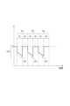
図2は、一例に係る高周波電力及びパルス状の負極性の直流電圧のタイミングチャートである。図2において、「VO」は、バイアス電源62の出力電圧を示しており、「RF」は、高周波電力RFのパワーレベルを示している。図2に示す例では、第1の部分期間P1は、パルス状の負極性の直流電圧PVが下部電極18に印加される期間である。図2に示す例では、第2の部分期間P2は、パルス状の負極性の直流電圧PVが下部電極18に印加されない期間である。図2に示す例では、第1の部分期間P1において高周波電力RFの一つのパルスPRFが供給されている。この例によれば、比較的高いエネルギーを有するイオンが基板Wに供給され得る。 FIG. 2 is a timing chart of the high frequency power and the pulsed negative DC voltage according to an example. In FIG. 2, "VO" indicates the output voltage of the
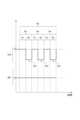
図3は、別の例に係る高周波電力及びパルス状の負極性の直流電圧のタイミングチャートである。図3において、「VO」は、バイアス電源62の出力電圧を示しており、「RF」は、高周波電力RFのパワーレベルを示している。図3に示す例では、第1の部分期間P1は、パルス状の負極性の直流電圧PVが下部電極18に印加されない期間である。図3に示す例では、第2の部分期間P2は、パルス状の負極性の直流電圧PVが下部電極18に印加される期間である。図3に示す例では、第1の部分期間P1において高周波電力RFの一つのパルスPRFが供給されている。この例によれば、比較的低いエネルギーを有するイオンが基板Wに供給され得る。 FIG. 3 is a timing chart of the high frequency power and the pulsed negative DC voltage according to another example. In FIG. 3, "VO" indicates the output voltage of the
図4は、更に別の例に係るパルス状の負極性の直流電圧のタイミングチャートである。図4において、「VO」は、バイアス電源62の出力電圧を示している。図4に示すように、パルス状の負極性の直流電圧PVの電圧レベルは、それが下部電極18に印加されている期間内において、変化してもよい。図4に示す例では、パルス状の負極性の直流電圧PVの電圧レベルは、それが下部電極18に印加されている期間内において、低下している。即ち、図4に示す例では、パルス状の負極性の直流電圧PVの電圧レベルの絶対値は、それが下部電極18に印加されている期間内において、増加している。なお、パルス状の負極性の直流電圧PVは、第1の部分期間P1において下部電極18に印加されてもよく、或いは、第2の部分期間P2において下部電極18に印加されてもよい。 FIG. 4 is a timing chart of a pulsed negative DC voltage according to yet another example. In FIG. 4, "VO" indicates the output voltage of the
図5は、更に別の例に係る高周波電力のタイミングチャートである。図5において、「RF」は、高周波電力RFのパワーレベルを示している。図5に示すように、制御部MCは、第1の部分期間P1において、高周波電力RFの複数のパルスPRFを順に供給するように高周波電源61を制御してもよい。即ち、制御部MCは、第1の部分期間P1において、複数のパルスPRFを含むパルス群PGを供給するように高周波電源61を制御してもよい。第1の部分期間P1において、高周波電力RFのパルスPRFは、周期的に供給されてもよい。第1の部分期間P1において高周波電力RFのパルスPRFが供給される周期PRFGを規定する周波数は、第2の周波数の2倍以上、且つ、第1の周波数の0.5倍以下であり得る。 FIG. 5 is a timing chart of radio frequency power according to yet another example. In FIG. 5, "RF" indicates the power level of the radio frequency power RF. As shown in FIG. 5, the control unit MC may control the radio frequency power supply61 to sequentially supply a plurality of pulses PRF of the radio frequency power RF in the first partial period P1. That is, the control unit MC may control the radio
図6は、更に別の例に係る高周波電力及びパルス状の負極性の直流電圧のタイミングチャートである。図6において、「VO」は、バイアス電源62の出力電圧を示しており、「RF」は、高周波電力RFのパワーレベルを示している。プラズマ処理装置1は、図2又は図3に示す例のように、期間PAにおいて、パルス状の負極性の直流電圧PVを周期PPで周期的に下部電極18に印加し、且つ、周期PP内において高周波電力RFの一つ以上のパルスPRFを供給する。図6に示すように、制御部MCは、別の期間PBにおいて、高周波電力RFの供給を停止するように高周波電源61を制御してもよい。期間PBにおいて、制御部MCは、高周波電力RFの供給が停止されている状態で、周期PPで周期的に下部電極18にパルス状の負極性の直流電圧PVを印加するようにバイアス電源62を制御してもよい。期間PBは、周期PPの時間長よりも長い時間長を有する期間である。期間PBは、チャンバ10内でプラズマが存在している期間であり得る。期間PBは、例えば、期間PAに続く期間であり得る。 FIG. 6 is a timing chart of the high frequency power and the pulsed negative DC voltage according to yet another example. In FIG. 6, "VO" indicates the output voltage of the
図7は、更に別の例に係る高周波電力及びパルス状の負極性の直流電圧のタイミングチャートである。図7において、「VO」は、バイアス電源62の出力電圧を示しており、「RF」は、高周波電力RFのパワーレベルを示している。図7に示すように、制御部MCは、別の期間PCにおいて、下部電極18に対するパルス状の負極性の直流電圧PVの印加を停止するようにバイアス電源62を制御してもよい。期間PCにおいて、制御部MCは、下部電極18に対するパルス状の負極性の直流電圧PVの印加が停止されている状態で、高周波電力RFを供給するように高周波電源61を制御してもよい。制御部MCは、期間PCにおいて、高周波電力RFのパルスPRF又はパルス群PGを周期的に供給するように高周波電源61を制御し得る。期間PCにおける高周波電力RFのパルスPRF又はパルス群PGの供給の周期PRFCは、期間PAにおける高周波電力RFのパルスPRF又はパルス群PGの供給の周期、即ち周期PPと同じ周期であり得る。なお、期間PCにおいても、パルス群PGを形成する高周波電力RFのパルスPRFの供給の周期PRFGを規定する周波数は、第2の周波数の2倍以上、且つ、第1の周波数の0.5倍以下であり得る。 FIG. 7 is a timing chart of the high frequency power and the pulsed negative DC voltage according to yet another example. In FIG. 7, "VO" indicates the output voltage of the
図8の(a)及び図8の(b)の各々は、更に別の例に係るパルス状の負極性の直流電圧のタイミングチャートである。図8の(a)に示す例におけるバイアス電源62の出力電圧VOは、その極性が第2の部分期間P2内且つ第1の部分期間P1の直前に正極性に変更されている点で、図2に示す例におけるバイアス電源62の出力電圧VOと異なっている。即ち、図8の(a)に示す例では、正極性の直流電圧が、第2の部分期間P2内且つ第1の部分期間P1の直前に、バイアス電源62から下部電極18に印加されている。なお、パルス状の負極性の直流電圧PVが第1の部分期間P1内に下部電極18に印加される場合には、第2の部分期間P2の少なくとも一部において、正極性の直流電圧がバイアス電源62から下部電極18に印加されてもよい。 Each of (a) of FIG. 8 and (b) of FIG. 8 is a timing chart of a pulsed negative DC voltage according to another example. The output voltage VO of the
図8の(b)に示す例におけるバイアス電源62の出力電圧VOは、その極性が第1の部分期間P1内且つ第2の部分期間P2の直前に正極性に変更されている点で、図3に示す例におけるバイアス電源62の出力電圧VOと異なっている。即ち、図8の(b)に示す例では、正極性の直流電圧が、第1の部分期間P1内且つ第2の部分期間P2の直前に、バイアス電源62から下部電極18に印加されている。なお、パルス状の負極性の直流電圧PVが第2の部分期間P2内に下部電極18に印加される場合には、第1の部分期間P1の少なくとも一部において、正極性の直流電圧がバイアス電源62から下部電極18に印加されてもよい。 The output voltage VO of the
以下、図9を参照する。図9は、一つの例示的実施形態に係るプラズマ処理方法を示す流れ図である。図9に示すプラズマ処理方法(以下、「方法MT」という)は、上述したプラズマ処理装置1を用いて実行され得る。Refer to FIG. 9 below. FIG. 9 is a flow chart showing a plasma processing method according to one exemplary embodiment. The plasma processing method shown in FIG. 9 (hereinafter, referred to as "method MT") can be performed using the plasma processing apparatus 1 described above.
方法MTは、静電チャック20上に基板Wが載置されている状態で実行される。方法MTは、基板Wにプラズマ処理を行うために実行される。方法MTでは、ガスがガス供給部からチャンバ10内に供給される。そして、チャンバ10内のガスの圧力が指定された圧力に排気装置50によって設定される。The method MT is performed with the substrate W placed on the
方法MTでは、工程ST1が実行される。工程ST1では、バイアス電源62から下部電極18にパルス状の負極性の直流電圧PVが周期PPで周期的に印加される。 In the method MT, a step ST1 is performed in which a pulsed negative DC voltage PV is periodically applied to the
工程ST2は、周期PP内の第1の部分期間P1において実行される。工程ST3は、周期PP内の第2の部分期間P2において実行される。第1の部分期間P1は、パルス状の負極性の直流電圧PVが下部電極18に印加される期間であってもよい。第2の部分期間P2は、パルス状の負極性の直流電圧PVが下部電極18に印加されない期間であってもよい。或いは、第1の部分期間P1は、パルス状の負極性の直流電圧PVが下部電極18に印加されない期間であってもよい。第2の部分期間P2は、パルス状の負極性の直流電圧PVが下部電極18に印加される期間であってもよい。 The process ST2 is performed in a first partial periodP1 in the cycleP1 . The process ST3 is performed in a second partial period P2 in the cycleP1 . The first partial periodP1 may be a period in which a pulsed negative DC voltage PV is appliedto the
工程ST2では、プラズマの生成のために、高周波電源61から高周波電力RFが供給される。第1の部分期間P1においては、高周波電力RFの一つ以上のパルスPRFが供給され得る。第1の部分期間P1においては、高周波電力RFの複数のパルスPRFが順に供給されてもよい。即ち、第1の部分期間P1において、複数のパルスPRFを含むパルス群PGが供給されてもよい。第1の部分期間P1において、高周波電力RFのパルスPRFは、周期的に供給されてもよい。第1の部分期間P1において高周波電力RFのパルスPRFが供給される周期PRFGを規定する周波数は、第2の周波数の2倍以上、且つ、第1の周波数の0.5倍以下であり得る。 In the process ST2, a high frequency power RF is supplied from the high
工程ST3では、周期PP内の第2の部分期間P2における高周波電力RFのパワーレベルが、第1の部分期間P1における高周波電力RFのパワーレベルから減少されたパワーレベルに設定される。第2の部分期間P2において高周波電力RFの供給は停止されてもよい。 In step ST3, the power level of the radio frequency power RF in the second partial periodP2 in the cycleP2 is set to a power level that is reduced from the power level of the radio frequency power RF in the first partial periodP1 . The supply of the radio frequency power RF in the second partial periodP2 may be stopped.
工程ST1~工程ST3は、上述した期間PAにおいて実行され得る。方法MTでは、期間PB(図6参照)において、高周波電源61からの高周波電力RFの供給が停止されている状態で、周期PPで周期的にバイアス電源62から下部電極18にパルス状の負極性の直流電圧PVが印加されてもよい。上述したように、期間PBは、周期PPの時間長よりも長い時間長を有する期間である。期間PBは、チャンバ10内でプラズマが存在している期間であり得る。期間PBは、例えば、期間PAに続く期間であり得る。 Steps ST1 to ST3 may be performed during the above-mentioned period PA. In the method MT, during the period PB (see FIG. 6 ), a pulsed negative DC voltage PV may be applied from the
方法MTでは、別の期間PC(図7参照)において、バイアス電源62からの下部電極18に対するパルス状の負極性の直流電圧PVの印加が停止されている状態で、高周波電源61から高周波電力RFが供給されてもよい。期間PCにおいて、制御部MCは、下部電極18に対するパルス状の負極性の直流電圧PVの印加が停止されている状態で、高周波電力RFを供給するように高周波電源61を制御してもよい。期間PCにおいては、高周波電力RFのパルスPRF又はパルス群PGが高周波電源61から周期的に供給されてもよい。期間PCにおける高周波電力RFのパルスPRF又はパルス群PGの供給の周期PRFCは、期間PAにおける高周波電力RFのパルスPRF又はパルス群PGの供給の周期、即ち周期PPと同じ周期であり得る。なお、期間PCにおいても、パルス群PGを形成する高周波電力RFのパルスPRFの供給の周期PRFGを規定する周波数は、第2の周波数の2倍以上、且つ、第1の周波数の0.5倍以下であり得る。 In the method MT, in another period PC (see FIG. 7 ), high frequency power RF may be supplied from the high
以上、種々の例示的実施形態について説明してきたが、上述した例示的実施形態に限定されることなく、様々な追加、省略、置換、及び変更がなされてもよい。また、異なる実施形態における要素を組み合わせて他の実施形態を形成することが可能である。Although various exemplary embodiments have been described above, various additions, omissions, substitutions, and modifications may be made without being limited to the exemplary embodiments described above. In addition, elements in different embodiments may be combined to form other embodiments.
別の実施形態に係るプラズマ処理装置は、プラズマ処理装置1とは異なる容量結合型のプラズマ処理装置であってもよい。また、更に別の実施形態に係るプラズマ処理装置は、誘導結合型プラズマ処理装置であってもよい。また、更に別の実施形態に係るプラズマ処理装置は、ECR(電子サイクロトロン共鳴)プラズマ処理装置であってもよい。また、更に別の実施形態に係るプラズマ処理装置は、マイクロ波といった表面波を用いてプラズマを生成するプラズマ処理装置であってもよい。The plasma processing apparatus according to another embodiment may be a capacitively coupled plasma processing apparatus different from the plasma processing apparatus 1. Furthermore, the plasma processing apparatus according to yet another embodiment may be an inductively coupled plasma processing apparatus. Furthermore, the plasma processing apparatus according to yet another embodiment may be an ECR (electron cyclotron resonance) plasma processing apparatus. Furthermore, the plasma processing apparatus according to yet another embodiment may be a plasma processing apparatus that generates plasma using surface waves such as microwaves.
また、周期PPは、第1の部分期間P1及び第2の部分期間P2を含む三つ以上の部分期間から構成されていてもよい。周期PP内の三つ以上の部分期間の時間長は、互いに同一であってもよく、互いに異なっていてもよい。三つ以上の部分期間の各々における高周波電力RFのパワーレベルは、前後の部分期間における高周波電力RFのパワーレベルとは異なるパワーレベルに設定され得る。 Furthermore, the periodP1 may be composed of three or more partial periods including a first partial periodP1 and a second partial periodP2 . The time lengths of the three or more partial periods in the periodP1 may be the same as each other or may be different from each other. The power level of the radio frequency power RF in each of the three or more partial periods may be set to a power level different from the power levels of the radio frequency power RF in the preceding and following partial periods.
以上の説明から、本開示の種々の実施形態は、説明の目的で本明細書で説明されており、本開示の範囲及び主旨から逸脱することなく種々の変更をなし得ることが、理解されるであろう。したがって、本明細書に開示した種々の実施形態は限定することを意図しておらず、真の範囲と主旨は、添付の特許請求の範囲によって示される。From the foregoing, it will be understood that the various embodiments of the present disclosure have been described herein for purposes of illustration, and that various modifications may be made without departing from the scope and spirit of the present disclosure. Accordingly, the various embodiments disclosed herein are not intended to be limiting, with the true scope and spirit being indicated by the appended claims.
1…プラズマ処理装置、10…チャンバ、16…基板支持器、18…下部電極、20…静電チャック、61…高周波電源、62…バイアス電源、MC…制御部。1...plasma processing apparatus, 10...chamber, 16...substrate support, 18...lower electrode, 20...electrostatic chuck, 61...high frequency power supply, 62...bias power supply, MC...control unit.
Claims (11)
Translated fromJapanese下部電極及び該下部電極上に設けられた静電チャックを有し、前記チャンバ内で、その上に載置される基板を支持するように構成された基板支持器と、
前記チャンバ内のガスからプラズマを生成するために供給される高周波電力を発生するように構成された高周波電源であり、該高周波電力は第1の周波数を有する、該高周波電源と、
前記下部電極に電気的に接続されており、前記第1の周波数よりも低い第2の周波数で規定される周期で周期的にパルス状の負極性の直流電圧を前記下部電極に印加するように構成されたバイアス電源と、
前記高周波電源を制御するように構成された制御部と、
を備え、
前記制御部は、
第1の期間に含まれる前記周期内の第1の部分期間内で前記高周波電力を供給し、前記周期内の第2の部分期間における前記高周波電力のパワーレベルを前記第1の部分期間における前記高周波電力のパワーレベルから減少されたパワーレベルに設定するように前記高周波電源を制御し、
前記チャンバ内でプラズマが存在している第2の期間であって前記第2の周波数で規定される前記周期の時間長よりも長い時間長を有する該第2の期間において、前記高周波電力の供給を停止するよう前記高周波電源を制御し、且つ、該第2の期間において、前記第2の周波数で規定される前記周期で周期的に前記下部電極に前記パルス状の負極性の直流電圧を印加するよう前記バイアス電源を制御する、
プラズマ処理装置。 A chamber;
a substrate support having a lower electrode and an electrostatic chuck disposed on the lower electrode, the substrate support being configured to support a substrate placed thereon within the chamber;
a radio frequency power supply configured to generate radio frequency power that is supplied to generate a plasma from gas in the chamber, the radio frequency power having a first frequency;
a bias power supply electrically connected to the lower electrode and configured to apply a negative DC voltage to the lower electrode in a pulsed manner at a period defined by a second frequency lower than the first frequency;
A control unit configured to control the high frequency power source;
Equipped with
The control unit is
supplying the high frequency power in a first partial period of the cycleincluded in a first period , and controlling the high frequency powersource to set a power level of the high frequency power in a second partial period of the cycle to a power level that is reduced from the power level of the high frequency power in the first partial period;
controlling the high frequency power supply to stop supplying the high frequency power during a second period during which plasma exists in the chamber, the second period having a time length longer than a time length of the cycle defined by the second frequency, and controlling the bias power supply to periodically apply the pulsed negative DC voltage to the lower electrode at the cycle defined by the second frequency during the second period.
Plasma processing equipment.
前記第2の部分期間は、前記パルス状の負極性の直流電圧が前記下部電極に印加されない期間である、
請求項1に記載のプラズマ処理装置。 the first partial period is a period during which the pulsed negative DC voltage is applied to the lower electrode,
the second partial period is a period during which the pulsed negative DC voltage is not applied to the lower electrode;
The plasma processing apparatus according to claim 1 .
前記第2の部分期間は、前記パルス状の負極性の直流電圧が前記下部電極に印加される期間である、
請求項1に記載のプラズマ処理装置。 the first partial period is a period during which the pulsed negative DC voltage is not applied to the lower electrode,
the second partial period is a period during which the pulsed negative DC voltage is applied to the lower electrode;
The plasma processing apparatus according to claim 1 .
該プラズマ処理装置は、
チャンバと、
下部電極及び該下部電極上に設けられた静電チャックを有し、前記チャンバ内で、その上に載置される基板を支持するように構成された基板支持器と、
前記チャンバ内のガスからプラズマを生成するために供給される高周波電力を発生するように構成された高周波電源であり、該高周波電力は第1の周波数を有する、該高周波電源と、
前記下部電極に電気的に接続されたバイアス電源と、
を備え、
該プラズマ処理方法は、前記静電チャック上に基板が載置されている状態で該基板にプラズマ処理を行うために実行され、
前記第1の周波数よりも低い第2の周波数で規定される周期で周期的に前記バイアス電源から前記下部電極にパルス状の負極性の直流電圧を印加する工程と、
第1の期間に含まれる前記周期内の第1の部分期間内で前記高周波電源から前記高周波電力を供給する工程と、
前記第1の期間に含まれる前記周期内の第2の部分期間内で前記高周波電力のパワーレベルを前記第1の部分期間における前記高周波電力のパワーレベルから減少されたパワーレベルに設定する工程と、
前記チャンバ内でプラズマが存在している第2の期間であって前記第2の周波数で規定される前記周期の時間長よりも長い時間長を有する該第2の期間において、前記高周波電源からの前記高周波電力の供給が停止されている状態で、前記第2の周波数で規定される該周期で周期的に前記バイアス電源から前記下部電極に前記パルス状の負極性の直流電圧を印加する工程と、
を含むプラズマ処理方法。 A plasma processing method using a plasma processing apparatus, comprising:
The plasma processing apparatus includes:
A chamber;
a substrate support having a lower electrode and an electrostatic chuck disposed on the lower electrode, the substrate support being configured to support a substrate placed thereon within the chamber;
a radio frequency power supply configured to generate radio frequency power that is supplied to generate a plasma from gas in the chamber, the radio frequency power having a first frequency;
a bias power supply electrically connected to the lower electrode;
Equipped with
The plasma processing method is carried out to perform a plasma processing on a substrate in a state where the substrate is placed on the electrostatic chuck,
applying a pulsed negative DC voltage from the bias power supply to the lower electrode periodically at a period defined by a second frequency lower than the first frequency;
supplying the high frequency power from the high frequency power source within a first partial period ofthe cycle included in a first period ;
setting a power level of the high frequency power within a second partial period ofthe cycle included in the first period to a power level that is reduced from the power level of the high frequency power within the first partial period;
applying the pulsed negative DC voltage from the bias power supply to the lower electrode periodically at the period defined by the second frequency in a state where the supply of high frequency power from the high frequency power supply is stopped during a second period during which plasma exists in the chamber, the second period having a time length longer than a time length of the period defined by the second frequency;
A plasma processing method comprising:
前記第2の部分期間は、前記パルス状の負極性の直流電圧が前記下部電極に印加されない期間である、
請求項6に記載のプラズマ処理方法。 the first partial period is a period during which the pulsed negative DC voltage is applied to the lower electrode,
the second partial period is a period during which the pulsed negative DC voltage is not applied to the lower electrode;
The plasma processing method according to claim6 .
前記第2の部分期間は、前記パルス状の負極性の直流電圧が前記下部電極に印加される期間である、
請求項6に記載のプラズマ処理方法。 the first partial period is a period during which the pulsed negative DC voltage is not applied to the lower electrode,
the second partial period is a period during which the pulsed negative DC voltage is applied to the lower electrode;
The plasma processing method according to claim6 .
Priority Applications (1)
| Application Number | Priority Date | Filing Date | Title |
|---|---|---|---|
| JP2024109623AJP7734239B2 (en) | 2019-01-09 | 2024-07-08 | Plasma processing apparatus and plasma processing method |
Applications Claiming Priority (6)
| Application Number | Priority Date | Filing Date | Title |
|---|---|---|---|
| JP2019001662 | 2019-01-09 | ||
| JP2019001662 | 2019-01-09 | ||
| JP2019018833 | 2019-02-05 | ||
| JP2019018833 | 2019-02-05 | ||
| PCT/JP2019/049499WO2020145051A1 (en) | 2019-01-09 | 2019-12-17 | Plasma treatment device and plasma treatment method |
| JP2020565660AJP7297795B2 (en) | 2019-01-09 | 2019-12-17 | Plasma processing apparatus and plasma processing method |
Related Parent Applications (1)
| Application Number | Title | Priority Date | Filing Date |
|---|---|---|---|
| JP2020565660ADivisionJP7297795B2 (en) | 2019-01-09 | 2019-12-17 | Plasma processing apparatus and plasma processing method |
Related Child Applications (1)
| Application Number | Title | Priority Date | Filing Date |
|---|---|---|---|
| JP2024109623ADivisionJP7734239B2 (en) | 2019-01-09 | 2024-07-08 | Plasma processing apparatus and plasma processing method |
Publications (2)
| Publication Number | Publication Date |
|---|---|
| JP2023115076A JP2023115076A (en) | 2023-08-18 |
| JP7519507B2true JP7519507B2 (en) | 2024-07-19 |
Family
ID=71521294
Family Applications (3)
| Application Number | Title | Priority Date | Filing Date |
|---|---|---|---|
| JP2020565660AActiveJP7297795B2 (en) | 2019-01-09 | 2019-12-17 | Plasma processing apparatus and plasma processing method |
| JP2023097775AActiveJP7519507B2 (en) | 2019-01-09 | 2023-06-14 | Plasma processing apparatus and plasma processing method |
| JP2024109623AActiveJP7734239B2 (en) | 2019-01-09 | 2024-07-08 | Plasma processing apparatus and plasma processing method |
Family Applications Before (1)
| Application Number | Title | Priority Date | Filing Date |
|---|---|---|---|
| JP2020565660AActiveJP7297795B2 (en) | 2019-01-09 | 2019-12-17 | Plasma processing apparatus and plasma processing method |
Family Applications After (1)
| Application Number | Title | Priority Date | Filing Date |
|---|---|---|---|
| JP2024109623AActiveJP7734239B2 (en) | 2019-01-09 | 2024-07-08 | Plasma processing apparatus and plasma processing method |
Country Status (7)
| Country | Link |
|---|---|
| US (1) | US20220084787A1 (en) |
| JP (3) | JP7297795B2 (en) |
| KR (1) | KR20210111269A (en) |
| CN (2) | CN119153304A (en) |
| SG (1) | SG11202107162UA (en) |
| TW (2) | TW202431904A (en) |
| WO (1) | WO2020145051A1 (en) |
Families Citing this family (24)
| Publication number | Priority date | Publication date | Assignee | Title |
|---|---|---|---|---|
| US10510575B2 (en) | 2017-09-20 | 2019-12-17 | Applied Materials, Inc. | Substrate support with multiple embedded electrodes |
| US11476145B2 (en) | 2018-11-20 | 2022-10-18 | Applied Materials, Inc. | Automatic ESC bias compensation when using pulsed DC bias |
| JP7297795B2 (en)* | 2019-01-09 | 2023-06-26 | 東京エレクトロン株式会社 | Plasma processing apparatus and plasma processing method |
| US11361947B2 (en)* | 2019-01-09 | 2022-06-14 | Tokyo Electron Limited | Apparatus for plasma processing and method of etching |
| KR102827481B1 (en) | 2019-01-22 | 2025-06-30 | 어플라이드 머티어리얼스, 인코포레이티드 | Feedback loop to control pulse voltage waveform |
| JP7511423B2 (en)* | 2019-12-17 | 2024-07-05 | 東京エレクトロン株式会社 | Plasma processing apparatus, plasma processing method, and power supply system |
| US11848176B2 (en) | 2020-07-31 | 2023-12-19 | Applied Materials, Inc. | Plasma processing using pulsed-voltage and radio-frequency power |
| TW202232567A (en)* | 2020-10-30 | 2022-08-16 | 日商東京威力科創股份有限公司 | Etching method and plasma processing apparatus |
| JP7309799B2 (en)* | 2020-10-30 | 2023-07-18 | 東京エレクトロン株式会社 | Etching method and plasma processing apparatus |
| US11901157B2 (en) | 2020-11-16 | 2024-02-13 | Applied Materials, Inc. | Apparatus and methods for controlling ion energy distribution |
| US11798790B2 (en) | 2020-11-16 | 2023-10-24 | Applied Materials, Inc. | Apparatus and methods for controlling ion energy distribution |
| JP7737401B2 (en)* | 2020-12-10 | 2025-09-10 | 東京エレクトロン株式会社 | Plasma processing method and plasma processing apparatus |
| JP7336608B2 (en)* | 2021-02-04 | 2023-08-31 | 東京エレクトロン株式会社 | Plasma processing apparatus and plasma processing method |
| US11791138B2 (en) | 2021-05-12 | 2023-10-17 | Applied Materials, Inc. | Automatic electrostatic chuck bias compensation during plasma processing |
| US11948780B2 (en) | 2021-05-12 | 2024-04-02 | Applied Materials, Inc. | Automatic electrostatic chuck bias compensation during plasma processing |
| US11967483B2 (en) | 2021-06-02 | 2024-04-23 | Applied Materials, Inc. | Plasma excitation with ion energy control |
| US11569066B2 (en) | 2021-06-23 | 2023-01-31 | Applied Materials, Inc. | Pulsed voltage source for plasma processing applications |
| US11476090B1 (en) | 2021-08-24 | 2022-10-18 | Applied Materials, Inc. | Voltage pulse time-domain multiplexing |
| US12106938B2 (en) | 2021-09-14 | 2024-10-01 | Applied Materials, Inc. | Distortion current mitigation in a radio frequency plasma processing chamber |
| CN118872034A (en)* | 2022-03-31 | 2024-10-29 | 东京毅力科创株式会社 | Plasma treatment equipment |
| US11972924B2 (en) | 2022-06-08 | 2024-04-30 | Applied Materials, Inc. | Pulsed voltage source for plasma processing applications |
| US12315732B2 (en) | 2022-06-10 | 2025-05-27 | Applied Materials, Inc. | Method and apparatus for etching a semiconductor substrate in a plasma etch chamber |
| US12272524B2 (en) | 2022-09-19 | 2025-04-08 | Applied Materials, Inc. | Wideband variable impedance load for high volume manufacturing qualification and on-site diagnostics |
| WO2025057636A1 (en)* | 2023-09-15 | 2025-03-20 | 東京エレクトロン株式会社 | Plasma processing device |
Citations (3)
| Publication number | Priority date | Publication date | Assignee | Title |
|---|---|---|---|---|
| JP2010219491A (en) | 2009-02-20 | 2010-09-30 | Tokyo Electron Ltd | Plasma etching method, plasma etching apparatus, and storage medium |
| JP2012054534A (en) | 2010-09-01 | 2012-03-15 | Samsung Electronics Co Ltd | Plasma etching method and apparatus therefor |
| JP2016152252A (en) | 2015-02-16 | 2016-08-22 | 東京エレクトロン株式会社 | Method for controlling potential of susceptor in plasma processing apparatus |
Family Cites Families (22)
| Publication number | Priority date | Publication date | Assignee | Title |
|---|---|---|---|---|
| KR100276736B1 (en)* | 1993-10-20 | 2001-03-02 | 히가시 데쓰로 | Plasma processing equipment |
| JP3700278B2 (en) | 1996-08-23 | 2005-09-28 | ソニー株式会社 | Manufacturing method of semiconductor device having dual gate structure |
| US6335535B1 (en)* | 1998-06-26 | 2002-01-01 | Nissin Electric Co., Ltd | Method for implanting negative hydrogen ion and implanting apparatus |
| JP2920188B1 (en)* | 1998-06-26 | 1999-07-19 | 日新電機株式会社 | Pulse bias hydrogen negative ion implantation method and implantation apparatus |
| JP4538209B2 (en)* | 2003-08-28 | 2010-09-08 | 株式会社日立ハイテクノロジーズ | Manufacturing method of semiconductor device |
| JP5221403B2 (en)* | 2009-01-26 | 2013-06-26 | 東京エレクトロン株式会社 | Plasma etching method, plasma etching apparatus and storage medium |
| JP2010238881A (en)* | 2009-03-31 | 2010-10-21 | Tokyo Electron Ltd | Plasma processing apparatus and plasma processing method |
| US8404598B2 (en)* | 2009-08-07 | 2013-03-26 | Applied Materials, Inc. | Synchronized radio frequency pulsing for plasma etching |
| KR102025540B1 (en) | 2012-08-28 | 2019-09-26 | 에이이에스 글로벌 홀딩스 피티이 리미티드 | Wide dynamic range ion energy bias control; fast ion energy switching; ion energy control and pulsed bias supply; and a virtual front panel |
| JP6224958B2 (en)* | 2013-02-20 | 2017-11-01 | 東京エレクトロン株式会社 | Plasma processing apparatus and plasma processing method |
| JP2015053384A (en)* | 2013-09-06 | 2015-03-19 | 東京エレクトロン株式会社 | Plasma processing method and plasma processing device |
| JP5701958B2 (en)* | 2013-10-15 | 2015-04-15 | 東京エレクトロン株式会社 | Substrate processing equipment |
| KR102124407B1 (en) | 2016-01-18 | 2020-06-18 | 주식회사 히타치하이테크 | Plasma processing method and plasma processing device |
| JP6479698B2 (en)* | 2016-02-18 | 2019-03-06 | 東芝メモリ株式会社 | Semiconductor manufacturing apparatus and semiconductor device manufacturing method |
| JP6770868B2 (en)* | 2016-10-26 | 2020-10-21 | 東京エレクトロン株式会社 | Method for impedance matching of plasma processing equipment |
| JP6697372B2 (en)* | 2016-11-21 | 2020-05-20 | キオクシア株式会社 | Dry etching method and semiconductor device manufacturing method |
| US10927449B2 (en)* | 2017-01-25 | 2021-02-23 | Applied Materials, Inc. | Extension of PVD chamber with multiple reaction gases, high bias power, and high power impulse source for deposition, implantation, and treatment |
| US10373804B2 (en) | 2017-02-03 | 2019-08-06 | Applied Materials, Inc. | System for tunable workpiece biasing in a plasma reactor |
| US12230475B2 (en)* | 2018-08-14 | 2025-02-18 | Tokyo Electron Limited | Systems and methods of control for plasma processing |
| JP7297795B2 (en)* | 2019-01-09 | 2023-06-26 | 東京エレクトロン株式会社 | Plasma processing apparatus and plasma processing method |
| CN116844934A (en)* | 2019-02-05 | 2023-10-03 | 东京毅力科创株式会社 | Plasma processing apparatus |
| JP7262375B2 (en)* | 2019-11-26 | 2023-04-21 | 東京エレクトロン株式会社 | Plasma processing method and plasma processing apparatus |
- 2019
- 2019-12-17JPJP2020565660Apatent/JP7297795B2/enactiveActive
- 2019-12-17USUS17/421,001patent/US20220084787A1/enactivePending
- 2019-12-17SGSG11202107162UApatent/SG11202107162UA/enunknown
- 2019-12-17CNCN202411261847.5Apatent/CN119153304A/enactivePending
- 2019-12-17CNCN201980087489.1Apatent/CN113228830B/enactiveActive
- 2019-12-17KRKR1020217023745Apatent/KR20210111269A/enactivePending
- 2019-12-17WOPCT/JP2019/049499patent/WO2020145051A1/ennot_activeCeased
- 2019-12-19TWTW113115655Apatent/TW202431904A/enunknown
- 2019-12-19TWTW108146683Apatent/TWI849020B/enactive
- 2023
- 2023-06-14JPJP2023097775Apatent/JP7519507B2/enactiveActive
- 2024
- 2024-07-08JPJP2024109623Apatent/JP7734239B2/enactiveActive
Patent Citations (3)
| Publication number | Priority date | Publication date | Assignee | Title |
|---|---|---|---|---|
| JP2010219491A (en) | 2009-02-20 | 2010-09-30 | Tokyo Electron Ltd | Plasma etching method, plasma etching apparatus, and storage medium |
| JP2012054534A (en) | 2010-09-01 | 2012-03-15 | Samsung Electronics Co Ltd | Plasma etching method and apparatus therefor |
| JP2016152252A (en) | 2015-02-16 | 2016-08-22 | 東京エレクトロン株式会社 | Method for controlling potential of susceptor in plasma processing apparatus |
Also Published As
| Publication number | Publication date |
|---|---|
| JP2023115076A (en) | 2023-08-18 |
| WO2020145051A1 (en) | 2020-07-16 |
| CN113228830A (en) | 2021-08-06 |
| SG11202107162UA (en) | 2021-07-29 |
| CN113228830B (en) | 2024-10-01 |
| JP7297795B2 (en) | 2023-06-26 |
| CN119153304A (en) | 2024-12-17 |
| JP7734239B2 (en) | 2025-09-04 |
| JPWO2020145051A1 (en) | 2021-11-18 |
| TW202042598A (en) | 2020-11-16 |
| JP2024133658A (en) | 2024-10-02 |
| TW202431904A (en) | 2024-08-01 |
| KR20210111269A (en) | 2021-09-10 |
| US20220084787A1 (en) | 2022-03-17 |
| TWI849020B (en) | 2024-07-21 |
Similar Documents
| Publication | Publication Date | Title |
|---|---|---|
| JP7519507B2 (en) | Plasma processing apparatus and plasma processing method | |
| US11742184B2 (en) | Plasma processing apparatus and plasma processing method | |
| KR102820562B1 (en) | Plasma processing apparatus and etching method | |
| JP7511423B2 (en) | Plasma processing apparatus, plasma processing method, and power supply system | |
| JP2024160333A (en) | Substrate support and plasma processing apparatus | |
| JP7710548B2 (en) | Plasma Processing Equipment | |
| JP7174687B2 (en) | Plasma processing apparatus and etching method | |
| JP7535438B2 (en) | Plasma processing apparatus and plasma processing method | |
| KR102857736B1 (en) | Plasma processing apparatus and plasma processing method | |
| KR102866883B1 (en) | Plasma processing apparatus and plasma processing method |
Legal Events
| Date | Code | Title | Description |
|---|---|---|---|
| A521 | Request for written amendment filed | Free format text:JAPANESE INTERMEDIATE CODE: A523 Effective date:20230712 | |
| A621 | Written request for application examination | Free format text:JAPANESE INTERMEDIATE CODE: A621 Effective date:20230712 | |
| TRDD | Decision of grant or rejection written | ||
| A01 | Written decision to grant a patent or to grant a registration (utility model) | Free format text:JAPANESE INTERMEDIATE CODE: A01 Effective date:20240611 | |
| A61 | First payment of annual fees (during grant procedure) | Free format text:JAPANESE INTERMEDIATE CODE: A61 Effective date:20240708 | |
| R150 | Certificate of patent or registration of utility model | Ref document number:7519507 Country of ref document:JP Free format text:JAPANESE INTERMEDIATE CODE: R150 |