Movatterモバイル変換


[0]ホーム

URL:


JP7499428B1 - Conductor crimping structure with connection terminal - Google Patents

Conductor crimping structure with connection terminal
Download PDF

Info

Publication number
JP7499428B1
JP7499428B1JP2024038979AJP2024038979AJP7499428B1JP 7499428 B1JP7499428 B1JP 7499428B1JP 2024038979 AJP2024038979 AJP 2024038979AJP 2024038979 AJP2024038979 AJP 2024038979AJP 7499428 B1JP7499428 B1JP 7499428B1
Authority
JP
Japan
Prior art keywords
conductor
crimping
layer plate
inner layer
connection terminal
Prior art date
Legal status (The legal status is an assumption and is not a legal conclusion. Google has not performed a legal analysis and makes no representation as to the accuracy of the status listed.)
Active
Application number
JP2024038979A
Other languages
Japanese (ja)
Other versions
JP2025139896A (en
Inventor
健一 三田村
次雄 安保
Current Assignee (The listed assignees may be inaccurate. Google has not performed a legal analysis and makes no representation or warranty as to the accuracy of the list.)
Union Machinery Co Ltd
Delta Plus Co Ltd
Original Assignee
Union Machinery Co Ltd
Delta Plus Co Ltd
Priority date (The priority date is an assumption and is not a legal conclusion. Google has not performed a legal analysis and makes no representation as to the accuracy of the date listed.)
Filing date
Publication date
Application filed by Union Machinery Co Ltd, Delta Plus Co LtdfiledCriticalUnion Machinery Co Ltd
Priority to JP2024038979ApriorityCriticalpatent/JP7499428B1/en
Application grantedgrantedCritical
Publication of JP7499428B1publicationCriticalpatent/JP7499428B1/en
Priority to EP24207170.2Aprioritypatent/EP4560838A1/en
Priority to CN202411636763.5Aprioritypatent/CN120049216A/en
Priority to US18/950,180prioritypatent/US20250174916A1/en
Publication of JP2025139896ApublicationCriticalpatent/JP2025139896A/en
Activelegal-statusCriticalCurrent
Anticipated expirationlegal-statusCritical

Links

Images

Landscapes

Abstract

Translated fromJapanese
Figure 0007499428000001

【課題】 電線の導体を導体圧着部により強固に圧着固定し、電気的接続の信頼性を確保する。
【解決手段】 導体圧着部3には、予め内層板3bと外層板3aとの二層構造による第1、第2圧着片3e、3fがU字状に立ち上げられている。また、各圧着片3e、3fの折り返し部の外層板3aと内層板3bとの間に空隙部3c、3dが形成されている。圧着片3e、3f間に単体から成る導体6を配置し、導体圧着装置のプレス上型Pu、プレス下型Pdにより、外層板3aと内層板3b、特に第1、第2圧着片3e、3fを押し潰すことにより、導体6を周囲から加締めて固定する。この加締めにおいて、下方から導体6の中心に向う押圧力、及び斜め上方から導体6の中心に向う2方向の押圧力を加えて、導体6に接するこれらの押圧部3k、3l、3m同士の間の内層板3bと導体6の間に3個所の非押圧部3n、3o、3pを設ける。
【選択図】図10

Figure 0007499428000001

The conductor of an electric wire is firmly crimped and fixed by a conductor crimping portion, thereby ensuring the reliability of the electrical connection.
[Solution] In the conductor crimping portion 3, the first and second crimping pieces 3e, 3f are raised in a U-shape in advance by a two-layer structure of an inner layer plate 3b and an outer layer plate 3a. In addition, gaps 3c, 3d are formed between the outer layer plate 3a and the inner layer plate 3b at the folded-back portions of each crimping piece 3e, 3f. A conductor 6 made of a single unit is placed between the crimping pieces 3e, 3f, and the outer layer plate 3a and the inner layer plate 3b, especially the first and second crimping pieces 3e, 3f, are crushed by the press upper die Pu and the press lower die Pd of the conductor crimping device, thereby crimping and fixing the conductor 6 from the periphery. In this crimping, a pressing force is applied from below toward the center of the conductor 6, and a pressing force is applied in two directions from diagonally above toward the center of the conductor 6, and three non-pressing parts 3n, 3o, 3p are provided between the inner layer plate 3b and the conductor 6 between the pressing parts 3k, 3l, 3m that contact the conductor 6.
[Selected figure] Figure 10

Description

Translated fromJapanese

本発明は、例えばコネクタハウジングに内装し、相手側コネクタの接続端子と嵌合する小型の接続端子による導体圧着構造に関するものである。The present invention relates to a conductor crimping structure using small connection terminals that are fitted inside a connector housing and engage with the connection terminals of a mating connector.

電気関係部品の小型化、軽量化、集積化に伴い、回路の接続に使用される接続端子には、より小型のものが常に要求されている。このことから、細線化された電線の導体に対応して、特許文献1に係る圧着接続端子が開示されている。As electrical components become smaller, lighter, and more integrated, there is a constant demand for smaller connection terminals used to connect circuits. For this reason, the crimp connection terminal inPatent Document 1 is disclosed to accommodate thinner electric wire conductors.

この特許文献1に係る圧着接続端子は、圧着片を二層構造とし、この二層構造の圧着片間に空隙部を形成し、細径の導体に対して加締め力を過大に加えて過度の変形等を与えることなく、この空隙部を維持する適度の弾発性を有する加締め力による加締めて固定することにより、撚線から成る細径の導体を確実に圧着接続することを可能としている。The crimp connection terminal according toPatent Document 1 has a two-layered crimp piece, a gap is formed between the two-layered crimp pieces, and the crimping force has a moderate elasticity to maintain the gap without excessively applying a crimping force to the thin conductor, causing excessive deformation, etc., making it possible to reliably crimp and connect thin conductors made of twisted wires.

従来においては、使用する導体は複数本の芯線を撚り合わせた撚線を用いるが合が殆どであって、導体自体が或る程度の柔軟性、可塑性を有している。従って、特許文献1のように空隙部を設けた圧着接続端子を用いて、適度の弾発性を有する加締め力により導体を圧着すれば、導体が細線であっても不自然に変形することがなく、また導電性等の電気的特性や引き抜き等の機械的特性を悪化させることはない。Conventionally, the conductors used are almost always twisted wires made by twisting together multiple core wires, and the conductors themselves have a certain degree of flexibility and plasticity. Therefore, if a crimp connection terminal with a gap is used as inPatent Document 1, and the conductor is crimped with a moderate elastic crimping force, the conductor will not unnaturally deform even if it is a thin wire, and electrical properties such as conductivity and mechanical properties such as pull-out will not deteriorate.

特開2020-71920号公報JP 2020-71920 A

しかし、近年においては、主に経済性の観点から、接続端子に接続する信号電線には、導体として単体の銅合金等の金属線の使用が試みられ、その直径も0.25~0.6mm程度の超細線とされている。However, in recent years, mainly from the perspective of economy, attempts have been made to use metal wires such as simple copper alloys as conductors for the signal wires that connect to the connection terminals, with the diameter being made into ultra-fine wires of around 0.25 to 0.6 mm.

このような単体から成る細線導体を従来の端子圧着片により接続する場合は、一般的には断面が図12に示すような単体の導体aを圧着片bにより全体を包み込む圧着構造になる。しかし、芯線を撚り合わせた導体とは異なり、単体の導体aは柔軟性、可塑性に乏しく剛体に近く、特に細線の導体aにあっては、圧着片bが導体aの周囲を均等な加締め力で加締めているとは限らず、必ずしも十分な機械固定力、電気導電性が得られない。When connecting such a thin conductor consisting of a single unit using a conventional terminal crimping piece, the crimping structure generally has a cross section as shown in Figure 12, in which the single conductor a is entirely wrapped by the crimping piece b. However, unlike a conductor made of twisted core wires, the single conductor a has little flexibility or plasticity and is close to a rigid body. In particular, in the case of a thin conductor a, the crimping piece b does not necessarily crimp the periphery of the conductor a with an even crimping force, and sufficient mechanical fixing force and electrical conductivity are not necessarily obtained.

しかも、単体から成る細径の導体を使用した場合には、特許文献1のような空隙部を有する圧着接続端子を用いても、なお導体を良好に圧着できないことが多く、機械的、電気的な問題が生じ易い。一方、通常の導体に対しては、導体の表面に発生し電気的障害となる酸化物や硫化物は圧着時に破壊されて除去し易いが、単体から成る細径の導体ではこの酸化物や硫化物の除去が極めて難しいという問題がある。Moreover, when using a thin conductor made of a single piece, even if a crimp connection terminal with a gap as inPatent Document 1 is used, the conductor still often cannot be crimped well, and mechanical and electrical problems are likely to occur. On the other hand, for normal conductors, oxides and sulfides that occur on the surface of the conductor and cause electrical interference are easily destroyed and removed during crimping, but with thin conductors made of a single piece, the problem is that it is extremely difficult to remove these oxides and sulfides.

本発明の目的は、上述の課題を解決し、単線から成る導体であっても、導体を確実に加締めて良好な固定力と導電性とを実現できる接続端子による導体圧着構造を提供することにある。The object of the present invention is to solve the above problems and provide a conductor crimping structure using a connection terminal that can reliably crimp the conductor and achieve good fixing force and conductivity, even if the conductor is made of a single wire.

上記目的を達成するための本発明に係る接続端子による導体圧着構造は、導電金属板を打抜き、折曲して導体圧着部を形成し、該導体圧着部の底部からU字状に立ち上げた一対の圧着片を有する圧着接続端子を用いて、前記圧着片により単体の金属線から成る断面円形の導体を加締めて固定した接続端子による導体圧着構造であって、前記各圧着片は、外層板と、該外層板の上端部の折り返し部から内側に折り返して前記外層板に積層した内層板とから成る二層構造であり、前記底部に対して上方左右に位置し、前記外層板と前記内層板との間の前記折り返し部の内側に、それぞれ空隙部を設け、前記内層板と前記導体との間には、前記底部及び一対の前記空隙部から前記導体の中心に向けて集中する3方向の押圧力によって前記内層板に対して変形を与えて形成される3個所の押圧部と、これらの押圧部同士の間に形成される3個所の非押圧部と備えることを特徴とする。The conductor crimping structure using a connection terminal according to the present invention, which is intended to achieve the above object, is a conductor crimping structure using a connection terminal in which a conductor crimping portion is formed by punching and bending a conductive metal plate, and a crimping connection terminal having a pair of crimping pieces that are raised in a U-shape from the bottom of the conductor crimping portion is used to crimp and fix a conductor having a circular cross section made of a single metal wire, and each of the crimping pieces has a two-layer structure consisting of an outer layer plate and an inner layer plate that is folded inward from the folded portion at the upper end of the outer layer plate and laminated on the outer layer plate, and is located on the left and right above the bottom, and has a gap portion on the inside of the folded portion between the outer layer plate and the inner layer plate, and between the inner layer plate and the conductor, three pressing portions are formed by deforming the inner layer plate by pressing forces in three directions that are concentrated from the bottom and the pair of gap portions toward the center of the conductor, and three non-pressing portions are formed between these pressing portions.

本発明に係る接続端子による導体圧着構造によれば、二層構造の圧着片に設けた空隙部を用いて導体を加締めると共に、導体に対し局部的に強い押圧力を集中する押圧部を3個所に設けると共に、これらの押圧部に隣接する3個所の圧着片と導体との間に非押圧部を設けることにより、導体に対する確実な加締めによる固定が可能で、機械的、電気的な信頼性を確保し得る。The conductor crimping structure of the connection terminal according to the present invention uses a gap provided in the two-layered crimping piece to crimp the conductor, and provides three pressure sections that locally concentrate a strong pressure force on the conductor. In addition, non-pressing sections are provided between the conductor and the three crimping pieces adjacent to these pressure sections, allowing the conductor to be securely crimped and fixed, ensuring mechanical and electrical reliability.

使用する圧着接続端子の斜視図である。FIG. 2 is a perspective view of a crimp connection terminal to be used.打抜いた導電金属板の平面図である。FIG. 2 is a plan view of a stamped conductive metal plate.折曲工程の一工程での導体圧着部の斜視図である。FIG. 11 is a perspective view of the conductor crimping portion in one step of a bending process.圧着前部の圧着片をU字状に立ち上げた状態の横断面図である。FIG. 11 is a cross-sectional view of the crimping piece at the front crimping portion raised into a U-shape.圧着後部の圧着片をU字状に立ち上げた状態の横断面図である。FIG. 11 is a cross-sectional view of the crimping piece at the rear of the crimping portion, in a state where the crimping piece is raised into a U-shape.圧着前部の第1、第2圧着片内に導体を配置した状態の説明図である。13 is an explanatory diagram of a state in which a conductor is disposed within the first and second crimping pieces of the front crimping portion. FIG.圧着前部の圧着工程1における断面構造図である。FIG. 2 is a cross-sectional structural view of the front crimping portion in crimpingstep 1.圧着前部の圧着工程2における断面構造図である。FIG. 13 is a cross-sectional structural view of the front crimping portion in crimpingstep 2.圧着前部の圧着工程3における断面構造図である。FIG. 13 is a cross-sectional structural view of the front crimping portion in crimpingstep 3.圧着前部の圧着工程4における断面構造図である。FIG. 13 is a cross-sectional structural view of the front crimping portion in crimpingstep 4.導体を圧着固定した状態の圧着接続端子の斜視図である。3 is a perspective view of the crimp connection terminal with the conductor crimped and fixed thereto; FIG.従来の圧着固定構造の断面図である。FIG. 1 is a cross-sectional view of a conventional crimping and fixing structure.

本発明を図1~図11に図示の実施例に基づいて詳細に説明する。
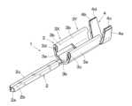
図1は本発明に係る接続端子による導体圧着構造で使用する実施例の圧着接続端子1の斜視図である。この圧着接続端子1は例えば厚さ0.1mmの薄肉の黄銅製であり、予め両表面に銅メッキ、スズメッキ等を施した1枚の導電金属板を打抜き、接続部、圧着部等が折曲により形成されている。
The present invention will be described in detail based on the embodiments shown in FIGS.
1 is a perspective view of acrimp connection terminal 1 according to an embodiment of the present invention, which is used in a conductor crimping structure using a connection terminal according to the present invention. Thecrimp connection terminal 1 is made of thin brass, for example 0.1 mm thick, and is punched out from a single conductive metal plate with both surfaces previously plated with copper or tin, and the connection portion, crimping portion, etc. are formed by bending.

圧着接続端子1の前方側には、相手側コネクタの接続端子と接続する例えば雄型挿入部である接続部2が形成され、後方側に導体圧着部3、被覆圧着部4が順次に配列されている。また、導体圧着部3は、長手方向に沿って前方から圧着前部3Xと圧着後部3Yとに区分されている。実際の圧着接続端子1には、コネクタハウジング内での姿勢を安定させるためのスタビライザや、コネクタハウジングに対する前後方向への抜け出しを防止するための係止部等が付設されることもあるが、これらの公知の機構の図示は省略している。The front side of thecrimp connection terminal 1 is formed with aconnection section 2, e.g. a male insertion section, which connects with the connection terminal of the mating connector, and theconductor crimping section 3 and theinsulation crimping section 4 are arranged in sequence on the rear side. Theconductor crimping section 3 is divided into acrimp front section 3X and a crimprear section 3Y from the front along the longitudinal direction. An actualcrimp connection terminal 1 may be provided with a stabilizer for stabilizing its position within the connector housing, a locking section for preventing it from slipping out of the connector housing in the forward and backward directions, and the like, but these well-known mechanisms are not shown in the figures.

図2は圧着接続端子1に成型する前の導電金属板5の打抜いた状態の平面図であり、接続部2、導体圧着部3、被覆圧着部4が素材として平面状に区画化されている。被覆圧着部4の更に後方には、打抜いた状態の圧着接続端子同士1を連結するための送り片5aが設けられており、各圧着接続端子1の後端の被覆圧着部4が連結片5bを介して送り片5aに接続されている。なお、送り片5aにはパイロット孔5cが設けられ、圧着接続端子1のその後の成型工程において、導電金属板5を間欠的に搬送するために使用される。Figure 2 is a plan view of theconductive metal plate 5 in a punched state before being formed into thecrimp connection terminal 1, with theconnection portion 2,conductor crimping portion 3, and coating crimpingportion 4 being partitioned into a planar shape as a material. Further behind thecoating crimping portion 4, afeed piece 5a is provided for connecting thecrimp connection terminals 1 in the punched state, and thecoating crimping portion 4 at the rear end of eachcrimp connection terminal 1 is connected to thefeed piece 5a via a connectingpiece 5b. Thefeed piece 5a is provided with apilot hole 5c, which is used to intermittently transport theconductive metal plate 5 in the subsequent molding process of thecrimp connection terminal 1.

このように打抜かれた導電金属板5は、例えば必要に応じて面取りや表面処理が行われた後に、送り片5aにより搬送されながら、フォーミングプレスによる各成型工程において、接続部2、導体圧着部3、被覆圧着部4が順次に折曲され、図1に示す圧着接続端子1に成型される。そして、成型後に連結片5bは切断され、各圧着接続端子1は個々に分離される。Theconductive metal plate 5 punched out in this manner is then subjected to chamfering or surface treatment as necessary, and then conveyed by thefeed piece 5a. In each forming process by the forming press, theconnection portion 2, theconductor crimping portion 3, and thecoating crimping portion 4 are successively bent, and formed into thecrimp connection terminal 1 shown in FIG. 1. After forming, the connectingpiece 5b is cut off, and eachcrimp connection terminal 1 is individually separated.

接続部2においては、図1、図2に示すように、導電金属板5の下板とする底板2aの両側から上板となる折返片2b、2cが、点線に沿って上側に折り返され、更に折返片2b、2cの両縁同士が突き合わされた二層構造の雄型挿込端とされている。なお、接続部2は他の雄型形状や、或いは雌型の受用接続部とする場合もある。As shown in Figures 1 and 2, in theconnection part 2, the foldedpieces 2b and 2c that form the upper plate are folded upward along the dotted lines from both sides of thebottom plate 2a that forms the lower plate of theconductive metal plate 5, and the edges of the foldedpieces 2b and 2c are butted together to form a two-layered male insertion end. Note that theconnection part 2 may have another male shape or may be a female receptacle connection part.

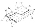
図2に示す導電金属板5では、圧着前部3X、圧着前部3Xはそれぞれ、中央に配置された外層板3aと、この外層板3aの両側から幅方向に延在され、幅方向の長さが異なる2枚の内層板3bとから構成されている。導体圧着部3の2本の長手方向の点線は、後述する折曲工程で外層板3aから内層板3bを内側に折り返す位置を示している。In theconductive metal plate 5 shown in FIG. 2, the crimpingfront portion 3X and the crimpingfront portion 3X are each composed of anouter layer plate 3a located in the center and twoinner layer plates 3b that extend widthwise from both sides of theouter layer plate 3a and have different width lengths. The two dotted lines in the longitudinal direction of theconductor crimping portion 3 indicate the positions where theinner layer plate 3b is folded inward from theouter layer plate 3a in the folding process described below.

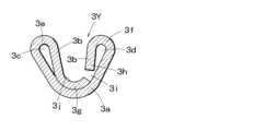
図3は折曲工程の1工程における導体圧着部3の斜視図である。圧着前部3X、圧着後部3Yでは、内層板3bが外層板3aの上端部からそれぞれ折り返し部において内側に折り返されて積層した二層構造とされている。そして、圧着前部3Xの片側の内層板3bの幅が長く延在され、圧着後部3Yでは他側の内層板3bの幅が長くされている。更に、圧着前部3X、圧着後部3Yの折り返し部の内層板3bと外層板3aの間のそれぞれには、断面が例えば水滴形状、風船形状、円形状、楕円形状等の空隙部3c、3dが形成されている。なお、圧着前部3Xの空隙部3cと圧着後部3Yの空隙部3dとは長手方向に連通し、圧着前部3Xの空隙部3dと圧着後部3Yの空隙部3cとは長手方向に連通している。Figure 3 is a perspective view of theconductor crimping portion 3 in one step of the bending process. In the front crimpingportion 3X and therear crimping portion 3Y, theinner layer plate 3b is folded inward from the upper end of theouter layer plate 3a at the folded portion to form a two-layer structure. The width of theinner layer plate 3b on one side of thefront crimping portion 3X is extended, and the width of theinner layer plate 3b on the other side of therear crimping portion 3Y is extended. Furthermore, between theinner layer plate 3b and theouter layer plate 3a of the folded portion of thefront crimping portion 3X and therear crimping portion 3Y, respectively,gaps 3c and 3d having a cross section of, for example, a water drop shape, a balloon shape, a circle shape, an ellipse shape, etc. are formed. Thegap 3c of thefront crimping portion 3X and thegap 3d of therear crimping portion 3Y are connected in the longitudinal direction, and thegap 3d of thefront crimping portion 3X and thegap 3c of therear crimping portion 3Y are connected in the longitudinal direction.

次の折曲工程において、圧着前部3X及び圧着後部3Yでは、両側の外層板3a、内層板3bをそれぞれ図4及び図5に示すように、第1、第2圧着片3e、3fとして、斜め上方に向けてU字状に立ち上げている。この状態において、圧着前部3Xと圧着後部3Yとは左右対称とされている。圧着前部3Xの第1圧着片3e側の内層板3bは外層板3aの上端部の折り返し部から下方に向けられ端縁部3gは外層板3aによる底部を覆い、更に第2圧着片3fの立ち上がり部の略中間位置にまで外層板3aに沿って長く延在されている。一方、第2圧着片3f側の内層板3bは外層板3aの上端部の折り返し部から下方に向けられ、端縁部3hは第2圧着片3fの立ち上がり部の略中間位置までと短く延在されている。そして、内層板3bの端縁部3g、端縁部3h同士との間には、外層板3a上に沿った隙間3iが形成されている。In the next folding process, theouter layer 3a and theinner layer 3b on both sides of the crimpedfront portion 3X and the crimpedrear portion 3Y are raised in a U-shape diagonally upward as the first and second crimpedpieces 3e and 3f, as shown in Figures 4 and 5, respectively. In this state, the crimpedfront portion 3X and the crimpedrear portion 3Y are bilaterally symmetrical. Theinner layer 3b on the first crimpedpiece 3e side of the crimpedfront portion 3X is directed downward from the folded portion of the upper end of theouter layer 3a, and theedge portion 3g covers the bottom portion of theouter layer 3a and further extends long along theouter layer 3a to approximately the middle position of the rising portion of the second crimpedpiece 3f. On the other hand, theinner layer 3b on the second crimpedpiece 3f side is directed downward from the folded portion of the upper end of theouter layer 3a, and theedge portion 3h is extended short to approximately the middle position of the rising portion of the second crimpedpiece 3f. Agap 3i is formed between theedge portions 3g and 3h of theinner layer plate 3b along theouter layer plate 3a.

このように、圧着前部3Xと圧着後部3Yとを左右対称としているのは、導体圧着部3の長さを大きくした場合に、後述する圧着工程において、導体に対する圧着力が左右不均衡となり易く、圧着接続端子1が捩れることを防止し、圧着力を左右均等に加えるためである。The reason why the front crimpingportion 3X andrear crimping portion 3Y are symmetrical in this way is that if the length of theconductor crimping portion 3 is increased, the crimping force on the conductor is likely to become unbalanced between the left and right in the crimping process described below, and this prevents thecrimp connection terminal 1 from twisting and applies the crimping force evenly to the left and right.

単体の導体6を圧着接続端子1により圧着接続するに際しては、先ず図6に示すように、絶縁被覆部が剥離された状態の、例えば直径0.32mmの例えば銅合金である金属線から成る導体6を、圧着接続端子1の長手方向に沿って圧着前部3Xの第1、第2圧着片3e、3fの間に挿入し、内層板3bの底部3j上に載置する。なお、圧着後部3Yにおいても、導体6に対する圧着は同時にかつ同様になされるので、以後の圧着工程は圧着前部3Xについてのみ説明する。When crimping asingle conductor 6 with acrimp connection terminal 1, first, as shown in FIG. 6, theconductor 6, which is a metal wire, for example, a copper alloy, with its insulating coating stripped off and having a diameter of, for example, 0.32 mm, is inserted between the first andsecond crimp pieces 3e, 3f of thecrimp front part 3X along the longitudinal direction of thecrimp connection terminal 1, and placed on thebottom part 3j of theinner layer plate 3b. Note that crimping of theconductor 6 is performed simultaneously and in the same way in the crimprear part 3Y, so the subsequent crimping process will only be described for thecrimp front part 3X.

導体圧着装置による導体6に対する圧着工程では、プレス上型Puとプレス下型Pdとの間に第1、第2圧着片3e、3fを配置した状態で、プレス上型Puの下降、プレス下型Pdの上昇を相対的に行う。なお、このプレス上型Pu、プレス下型Pdは、圧着前部3Xと圧着後部3Yとを区別することなく一体に作動するようにされている。In the process of crimping theconductor 6 by the conductor crimping device, the upper press die Pu is lowered and the lower press die Pd is raised relative to the first andsecond crimping pieces 3e, 3f, which are positioned between the upper press die Pu and the lower press die Pd. The upper press die Pu and the lower press die Pd are designed to operate together without distinguishing between the front crimpingpart 3X and the rear crimpingpart 3Y.

プレス上型Pu、プレス下型Pdとの作動により、図7に示すように、第1、第2圧着片3e、3fはプレス上型Pu、プレス下型Pdの形状に従って導体6を包み込むように変形する。この過程で、第1、第2圧着片3e、3fへの加締めにより、内層板3bの端縁部3g、3h間の隙間3iは縮小され、空隙部3c、3dの大きさも縮小され、外層板3aの側面はプレス上型Puにより立ち上げられ、外層板3a、内層板3bによる底部は、プレス下型Pdに沿ってU字形から偏平状に変形する。By the operation of the press upper die Pu and press lower die Pd, the first andsecond crimping pieces 3e, 3f are deformed to encase theconductor 6 according to the shapes of the press upper die Pu and press lower die Pd, as shown in Figure 7. During this process, thegap 3i between theedge portions 3g, 3h of theinner layer plate 3b is reduced by the crimping of the first and second crimpingpieces 3e, 3f, and the size of thevoids 3c, 3d is also reduced, the side of theouter layer plate 3a is raised by the press upper die Pu, and the bottom portion formed by theouter layer plate 3a andinner layer plate 3b is deformed from a U-shape to a flattened shape along the press lower die Pd.

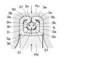
更に、図8に示すようにプレス上型Puとプレス下型Pdの作動により、強い加締め力が第1、第2圧着片3e、3fに加えることにより、第1、第2圧着片3e、3fは更に導体6を包み込むように変形する。このとき、導体6には主に矢印で示す3方向からの押圧力、つまり、底部3jから導体6の中心に向う導体6への上方向の押圧力、及び底部3jに対して上方左右に位置する空隙部3c、3dから導体6の中心に向う導体6への斜め下方向の押圧力が加えられる。そして、これらの導体6の中心に向けて集中して掛かる押圧力の3方向の角度は、約120度間隔とされている。Furthermore, as shown in FIG. 8, by operating the press upper die Pu and press lower die Pd, a strong crimping force is applied to the first andsecond crimping pieces 3e, 3f, which deform further to encase theconductor 6. At this time, theconductor 6 is subjected to pressure forces mainly from three directions indicated by arrows, that is, an upward pressure force from thebottom 3j toward the center of theconductor 6, and a diagonally downward pressure force from thegaps 3c, 3d located above and to the left and right of thebottom 3j toward the center of theconductor 6. The angles of the three directions of the pressure forces concentrated toward the center of theconductor 6 are spaced at intervals of approximately 120 degrees.

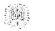
更なる加締めにより、図9に示すように、第1、第2圧着片3e、3fでは、加締め過程で外層板3a、内層板3bの厚みが増加すると共に、空隙部3c、3dの大きさは更に縮小される。この加締め過程で、プレス上型Pu、プレス下型Pdによる押圧力を特に前述の3方向から局部的に集中させ、この押圧力を集中させた3個所において、内層板3dが導体6に接する押圧部3k、3l、3mを設けると共に、これらの押圧部3k、3l、3m同士の間の導体6に沿った3個所においては、内層板3dから導体6に対して押圧力を加えることがなく、この部分における内層板3dと導体6の間に3個所の非押圧部3n、3o、3pを設ける。As a result of further crimping, as shown in Figure 9, the thickness of theouter layer plate 3a and theinner layer plate 3b increases during the crimping process in the first and second crimpingpieces 3e and 3f, and the size of thegaps 3c and 3d is further reduced. During this crimping process, the pressing force from the press upper die Pu and the press lower die Pd is concentrated locally, particularly from the three directions mentioned above, and at the three locations where this pressing force is concentrated,pressing parts 3k, 3l, and 3m are provided where theinner layer plate 3d contacts theconductor 6, and at three locations along theconductor 6 between thesepressing parts 3k, 3l, and 3m, no pressing force is applied from theinner layer plate 3d to theconductor 6, and threenon-pressing parts 3n, 3o, and 3p are provided between theinner layer plate 3d and theconductor 6 in these locations.

即ち、導体6の外周面に対して導体6を固定する押圧力を3個所に集中させることにより、押圧部3k、3l、3mにおいて導体6のこの部分の酸化物や硫化物から成る被膜を破壊しこれを除去して、内層板3dとの間における電気的接続の信頼性を高めることができる。In other words, by concentrating the pressing force that fixes theconductor 6 to the outer periphery of theconductor 6 at three points, the coating made of oxides and sulfides on this part of theconductor 6 atpressing parts 3k, 3l, and 3m is destroyed and removed, thereby improving the reliability of the electrical connection between theinner layer plate 3d.

プレス上型Pu、プレス下型Pdによる押圧によって、内層板3bと導体6との間に、押圧部3k、3l、3mと非押圧部3n、3o、3pとが形成されるまでの間には、概ね次のような現象が発生している。By the time the pressing by the upper press die Pu and the lower press die Pd forms the pressedparts 3k, 3l, 3m and thenon-pressed parts 3n, 3o, 3p between theinner layer board 3b and theconductor 6, the following phenomena generally occur:

外層板3aは、プレス上型Pu、プレス下型Pdによる押圧力を受けて変形し、降伏点を超えると塑性変形する。従って、プレス上型Pu、プレス下型Pdによる押圧を解除しても、外層板3aは元の形状に戻ることはない。これに対し、内層板3bは、プレス上型Pu、プレス下型Pdによる押圧力を、外層板3aを介して受けている。内層板3bのうち、外層板3aに沿って延在する部分においては、外層板3aに沿った形状に塑性変形する。Theouter layer plate 3a is deformed by the pressing force of the upper press die Pu and the lower press die Pd, and undergoes plastic deformation when it exceeds its yield point. Therefore, even if the pressing force of the upper press die Pu and the lower press die Pd is released, theouter layer plate 3a does not return to its original shape. In contrast, theinner layer plate 3b receives the pressing force of the upper press die Pu and the lower press die Pd through theouter layer plate 3a. The portion of theinner layer plate 3b that extends along theouter layer plate 3a undergoes plastic deformation into a shape that follows theouter layer plate 3a.

なお、内層板3bのうち、空隙部3c、3dに沿って延在する部分においては、外層板3aを介して内層板3bに掛かる押圧力は、内層板3bの端縁部3g、3h間の隙間3iを縮小させることに費やされた後に、空隙部3c、3dを縮小させることに使われることになる。このため、外層板3aにかかる押圧力が外層板3aの降伏点を超えたからといって、直ちに内層板3bにかかる押圧力も内層板3bの降伏点を超えるものとはならない。そこで、このような外層板3aと内層板3bとの間に存在する押圧力の掛かり方の違いを利用することによって、内層板3bに生ずる変形において、その全部を塑性変形へと至らしめることなく、弾性変形に留まる部分を残すことができる。In the portion of theinner layer 3b that extends along thegaps 3c and 3d, the pressing force applied to theinner layer 3b through theouter layer 3a is used to reduce thegap 3i between theedge portions 3g and 3h of theinner layer 3b, and is then used to reduce thegaps 3c and 3d. Therefore, even if the pressing force applied to theouter layer 3a exceeds the yield point of theouter layer 3a, the pressing force applied to theinner layer 3b does not immediately exceed the yield point of theinner layer 3b. Therefore, by utilizing the difference in the way the pressing force is applied between theouter layer 3a and theinner layer 3b, it is possible to prevent the entire deformation of theinner layer 3b from becoming plastic, and to leave a portion that remains elastically deformed.

従って、プレス上型Pu、プレス下型Pdによる押圧を解除すると、内層板3bにおいて、弾性変形により縮小した空隙部3c、3dが元の大きさへと拡大しようとする弾性復元力が生ずる。この弾性復元力は、内層板3bのうち、空隙部3c、3dに沿って延在する部分を外層板3aから離間させる方向に、つまり内方へと押し戻そうとする。このとき、内方へと押し戻されようとする内層板3bは、導体6と接して導体6を押圧し、内層板3bは導体6に対して付勢力を伴って接し、導体6が内層板3bの間に圧着されることになる。Therefore, when the pressure from the upper press die Pu and the lower press die Pd is released, an elastic restoring force is generated in theinner layer plate 3b, which causes thegaps 3c and 3d, which have been reduced in size by elastic deformation, to expand to their original size. This elastic restoring force tries to push the parts of theinner layer plate 3b that extend along thegaps 3c and 3d in a direction that separates them from theouter layer plate 3a, that is, inward. At this time, theinner layer plate 3b, which is being pushed back inward, comes into contact with theconductor 6 and presses it, and theinner layer plate 3b comes into contact with theconductor 6 with a biasing force, and theconductor 6 is crimped between theinner layer plates 3b.

そして、本実施例はこのような加締めを可能とする第1、第2圧着片3e、3fと、単体から成る導体6とを組み合わせることによって、次のような作用効果が得られることになる。In this embodiment, by combining the first and second crimpingpieces 3e and 3f, which enable such crimping, with theconductor 6, which is made of a single piece, the following effects are obtained.

導体が複数本の芯線を撚り合わせて成る場合においては、各芯線の間に隙間が存在するため、導体が内層板3bによって押圧されると、各芯線は互いの間の隙間を埋めるようにして移動する。その結果、導体の全体としての形状は、内層板3bに囲まれた空間の形状に沿う形状へと変化する。このため、内層板3bからの押圧力は各芯線を移動させることに使われるため、各芯線が内層板3bから受ける押圧力は、導体が単線のものから成る場合に比較して小さい。このことに応じて、各芯線の表面を覆う酸化物等の被膜が破壊される程度もまた小さいものとなる。When a conductor is made of multiple twisted core wires, there are gaps between each core wire, so when the conductor is pressed by theinner layer plate 3b, the core wires move to fill the gaps between them. As a result, the overall shape of the conductor changes to a shape that conforms to the shape of the space surrounded by theinner layer plate 3b. Because the pressing force from theinner layer plate 3b is used to move each core wire, the pressing force that each core wire receives from theinner layer plate 3b is smaller than when the conductor is made of a single wire. Accordingly, the degree to which the oxide or other coating that covers the surface of each core wire is destroyed is also smaller.

これに対し、導体6が単体である場合においては、導体が撚線の場合のように芯線の移動を伴わないことから、内層板3bからの押圧力は導体6の3個所に集中して掛かり続けることとなる。その結果として、導体6と内層板3bとの接触面積は小さくなるものの、導体6と内層板3bとが接する3個所の押圧部3k、3l、3mにおいて、大きな付勢力を伴う接触を可能とし、十分な機械的性能、電気的性能が得られ、更には酸化物等から成る被膜の破壊除去をも可能とする。In contrast, when theconductor 6 is a single piece, the core wire does not move as in the case of a stranded conductor, and the pressing force from theinner layer plate 3b continues to be concentrated at three points on theconductor 6. As a result, although the contact area between theconductor 6 and theinner layer plate 3b is small, contact with a large pressing force is possible at the threepressing points 3k, 3l, and 3m where theconductor 6 and theinner layer plate 3b come into contact, resulting in sufficient mechanical and electrical performance, and even enabling the destruction and removal of the coating made of oxides, etc.

上述の作用効果は、導体として撚線を採用した場合からは、予見することができず、単体の導体6を使用する本発明において新たに見出されたものである。即ち、導体として複数本の芯線を撚り合わせて成るものを採用した場合には、断面において周面で接触するに対し、導体として単線を採用した場合には複数の点で接触することにおいて、両者の発想は互いに異なる。The above-mentioned effects could not be predicted when a twisted wire is used as the conductor, but were newly discovered in the present invention, which uses asingle conductor 6. That is, when a conductor made of multiple twisted core wires is used, the conductor makes contact at the circumferential surface in cross section, whereas when a solid wire is used as the conductor, the conductor makes contact at multiple points, and the two concepts are different.

このように、空隙部3c、3dに加えて、導体6の上方及び下方両側と内層板3bとの間に、3個所の非押圧部3n、3o、3pを設けて、外層板3a、内層板3bにより導体6を加締めることにより、図10に示すように、空隙部3c、3d、非押圧部3n、3o、3pが更に縮小された接続端子による導体圧着構造が得られる。この構造により、導体6への加締めは、弾力性を保持しながら確実になされ、電気的、機械的な信頼性が確保されることになる。In this way, in addition to thegaps 3c and 3d, threenon-pressurized portions 3n, 3o, and 3p are provided between the upper and lower sides of theconductor 6 and theinner plate 3b, and theconductor 6 is crimped by theouter plate 3a and theinner plate 3b, resulting in a conductor crimping structure with a connection terminal in which thegaps 3c, 3d and thenon-pressurized portions 3n, 3o, and 3p are further reduced, as shown in Figure 10. With this structure, theconductor 6 is crimped reliably while retaining its elasticity, ensuring electrical and mechanical reliability.

なお図10においては、3個所の押圧部3n、3o、3pに空隙が生じているように図示しており、導体6に対して3個所の押圧部3k、3l、3mによる3方向からの付勢力を伴う接触がなされている。導体6を押圧部3k、3l、3mにより加締めて圧着固定した際に、非押圧部3n、3o、3pが形成されるが、これらの非押圧部3o、3pについては、非押圧状態で内層板3bと導体6とを接触させて空隙が生じないようにしてもよい。In FIG. 10, the threepressing parts 3n, 3o, and 3p are shown as having gaps, and the threepressing parts 3k, 3l, and 3m are in contact with theconductor 6 with a biasing force from three directions. When theconductor 6 is crimped and fixed by thepressing parts 3k, 3l, and 3m, thenon-pressing parts 3n, 3o, and 3p are formed, but for thesenon-pressing parts 3o and 3p, theinner layer plate 3b and theconductor 6 may be in contact in a non-pressing state to prevent gaps from being generated.

つまり、底部3jからの押圧力の上方向と空隙部3cからの押圧力の左下斜め方向との間に形成される非押圧部3oと、底部3jからの押圧力の上方向と空隙部3dからの右下斜め方向との間に形成される非押圧部3pに対しては、内層板3bと導体6とを接触させて空隙が生じないようにし、空隙部3cからの押圧力の左下斜め方向と空隙部3dからの右下斜め方向との間に形成される非押圧部3nのみに空隙が生ずるようにしてもよい。更には、非押圧部3n、3o、3pの全てが、非押圧状態で内層板3bと導体6とを接触させて空隙が生じないようにすることもできる。In other words, theinner layer plate 3b and theconductor 6 may be in contact with each other to prevent gaps from being generated for the non-pressed portion 3o formed between the upward direction of the pressing force from the bottom 3j and the downward left diagonal direction of the pressing force from thegap 3c, and thenon-pressed portion 3p formed between the upward direction of the pressing force from the bottom 3j and the downward right diagonal direction from thegap 3d, and a gap may be generated only in thenon-pressed portion 3n formed between the downward left diagonal direction of the pressing force from thegap 3c and the downward right diagonal direction from thegap 3d. Furthermore, it is also possible to prevent gaps from being generated for all of thenon-pressed portions 3n, 3o, and 3p by contacting theinner layer plate 3b and theconductor 6 in an unpressed state.

このようにして、プレス上型Pu、プレス下型Pdによる押圧によって、内層板3bと導体6との間には、底部3j及び空隙部3c、3dが存在する3方向から導体6の中心に向けて押圧力を集中する。これにより、内層板3bに対して変形を与えて形成される3個所の押圧部3k、3l、3mと、これらの押圧部3k、3l、3mの形成に伴い押圧部3k、3l、3m同士の間に形成される3個所の非押圧部3n、3o、3pとが存在することになる。In this way, by pressing with the upper press die Pu and the lower press die Pd, pressing forces are concentrated between theinner layer plate 3b and theconductor 6 from three directions, where the bottom 3j and thegaps 3c and 3d exist, toward the center of theconductor 6. This results in three pressedparts 3k, 3l, and 3m formed by deforming theinner layer plate 3b, and threenon-pressed parts 3n, 3o, and 3p formed between the pressedparts 3k, 3l, and 3m as a result of the formation of these pressedparts 3k, 3l, and 3m.

また、被覆圧着部4においては、導体圧着装置と連動する被覆圧着装置によって、絶縁被覆部7の外側を被覆圧着部4の一対の被覆圧着片4a、4bにより加締めることにより、辺部4c、4dが絶縁被覆部7に喰い込むようにして圧着される。これにより、被覆圧着部4により絶縁被覆部7を固定し、電線に作用する引抜力に対抗することができる。In addition, in thecoating crimping part 4, the outer side of the insulating coating part 7 is crimped by a pair ofcoating crimping pieces 4a, 4b of thecoating crimping part 4 using a coating crimping device that works in conjunction with the conductor crimping device, so that thesides 4c, 4d are crimped so as to bite into the insulating coating part 7. This allows the insulating coating part 7 to be fixed by thecoating crimping part 4 and to resist the pulling force acting on the electric wire.

図11は導体6を導体圧着部3の圧着前部3X、圧着後部3Yにより圧着接続し、被覆圧着部4では被覆圧着片4a、4bにより絶縁被覆部7を圧着固定した状態を示している。Figure 11 shows the state in which theconductor 6 is crimped and connected by thefront crimping part 3X and rear crimpingpart 3Y of theconductor crimping part 3, and the insulating coating part 7 is crimped and fixed by thecoating crimping pieces 4a and 4b in thecoating crimping part 4.

なお、実施例においては、導体圧着部3は前後に圧着前部3Xと圧着後部3Yに分けて設けたが、このように分けることなく、導体圧着部3の全体をこれらの何れか一方のみの形状とすることもできる。また、内層板3bの長さは左右均等な長さとし、左右対称形としてもよい。In the embodiment, theconductor crimping section 3 is divided into a front crimpingsection 3X and arear crimping section 3Y, but the entireconductor crimping section 3 may have only one of these shapes without being divided in this way. Also, the length of theinner layer plate 3b may be equal on the left and right, and may be symmetrical on the left and right.

更に、実施例においては、空隙部3c、3dを圧着接続端子1に予め形成しておいたが、導体圧着工程時において、プレス上型Puの形状によって、外層板3aと内層板3bとの間に空隙部3c、3dを形成することもできる。Furthermore, in the embodiment, thegaps 3c and 3d are formed in advance in thecrimp connection terminal 1, but during the conductor crimping process, thegaps 3c and 3d can also be formed between theouter layer plate 3a and theinner layer plate 3b depending on the shape of the press upper die Pu.

1 圧着接続端子
2 接続部
3 導体圧着部
3X 圧着前部
3Y 圧着後部
3a 外層板
3b 内層板
3c、3d 空隙部
3e、3f 圧着片
3k、3l、3m 押圧部
3n、3o、3p 非押圧部
4 被覆圧着部
5 導電金属板
6 導体
7 絶縁被覆部
REFERENCE SIGNSLIST 1Crimp connection terminal 2Connection portion 3Conductor crimping portion 3X Crimpingfront portion 3Y Crimpingrear portion 3aOuter layer plate 3bInner layer plate 3c,3d Space portion 3e, 3f Crimpingpiece 3k, 3l,3m Pressing portion 3n, 3o, 3pNon-pressing portion 4Covering crimping portion 5Conductive metal plate 6 Conductor 7 Insulating cover portion

Claims (4)

Translated fromJapanese
導電金属板を打抜き、折曲して導体圧着部を形成し、該導体圧着部の底部からU字状に立ち上げた一対の圧着片を有する圧着接続端子を用いて、前記圧着片により単体の金属線から成る断面円形の導体を加締めて固定した接続端子による導体圧着構造であって、
前記各圧着片は、外層板と、該外層板の上端部の折り返し部から内側に折り返して前記外層板に積層した内層板とから成る二層構造であり、
前記底部に対して上方左右に位置し、前記外層板と前記内層板との間の前記折り返し部の内側に、それぞれ空隙部を設け、
前記内層板と前記導体との間には、前記底部及び一対の前記空隙部から前記導体の中心に向けて集中する3方向の押圧力によって前記内層板に対して変形を与えて形成される3個所の押圧部と、これらの押圧部同士の間に形成される3個所の非押圧部と備えることを特徴とする接続端子による導体圧着構造。
A conductor crimping structure using a connection terminal, in which a conductor crimping portion is formed by punching and bending a conductive metal plate, and a crimping connection terminal having a pair of crimping pieces standing up in a U-shape from a bottom of the conductor crimping portion is used to crimp and fix a conductor having a circular cross section made of a single metal wire by the crimping pieces,
Each of the pressure-bonding pieces has a two-layer structure including an outer layer plate and an inner layer plate folded inward from a folded-back portion at an upper end of the outer layer plate and laminated on the outer layer plate,
A gap is provided on the left and right sides of the bottom and on the inside of the folded portion between the outer layer board and the inner layer board,
A conductor crimping structure using a connection terminal, characterized in that between the inner layer plate and the conductor, there are three pressed portions formed by deforming the inner layer plate by three-directional pressing forces concentrated from the bottom and a pair of the void portions toward the center of the conductor, and three non-pressed portions formed between these pressed portions.
前記3個所の前記非押圧部のうち、少なくとも前記底部の斜め両側に形成される2個所の前記非押圧部においては、前記内層板は前記導体に非押圧状態で接触していることを特徴とする請求項1に記載の接続端子による導体圧着構造。The conductor crimping structure using the connection terminal described in claim 1, characterized in that, of the three non-pressed portions, at least two non-pressed portions formed on both diagonal sides of the bottom portion are in contact with the conductor in a non-pressed state. 前記導体に対する前記3方向の押圧力は、略120度間隔の方向から加えたことを特徴とする請求項1に記載の接続端子による導体圧着構造。The conductor crimping structure using the connection terminal according to claim 1, characterized in that the three directional pressure forces on the conductor are applied from directions spaced approximately 120 degrees apart. 前記外層板と前記内層板との間に設けた前記空隙部は、前記圧着接続端子に予め形成しておいたことを特徴とする請求項1に記載の接続端子による導体圧着構造。The conductor crimping structure using the connection terminal according to claim 1, characterized in that the gap between the outer layer plate and the inner layer plate is formed in advance in the crimp connection terminal.
JP2024038979A2023-11-242024-03-13 Conductor crimping structure with connection terminalActiveJP7499428B1 (en)

Priority Applications (4)

Application NumberPriority DateFiling DateTitle
JP2024038979AJP7499428B1 (en)2024-03-132024-03-13 Conductor crimping structure with connection terminal
EP24207170.2AEP4560838A1 (en)2023-11-242024-10-17Conductor crimp structure using connection terminal
CN202411636763.5ACN120049216A (en)2023-11-242024-11-15Conductor press-connection structure for connecting terminal
US18/950,180US20250174916A1 (en)2023-11-242024-11-18Conductor crimp structure using connection terminal

Applications Claiming Priority (1)

Application NumberPriority DateFiling DateTitle
JP2024038979AJP7499428B1 (en)2024-03-132024-03-13 Conductor crimping structure with connection terminal

Publications (2)

Publication NumberPublication Date
JP7499428B1true JP7499428B1 (en)2024-06-13
JP2025139896A JP2025139896A (en)2025-09-29

Family

ID=91377593

Family Applications (1)

Application NumberTitlePriority DateFiling Date
JP2024038979AActiveJP7499428B1 (en)2023-11-242024-03-13 Conductor crimping structure with connection terminal

Country Status (1)

CountryLink
JP (1)JP7499428B1 (en)

Citations (2)

* Cited by examiner, † Cited by third party
Publication numberPriority datePublication dateAssigneeTitle
JP6506877B1 (en)2018-10-292019-04-24株式会社デルタプラス Crimp connection terminal
JP2021144898A (en)2020-03-132021-09-24株式会社デルタプラスMethod for terminal crimp to wire conductor and crimp connection terminal used for the method

Patent Citations (2)

* Cited by examiner, † Cited by third party
Publication numberPriority datePublication dateAssigneeTitle
JP6506877B1 (en)2018-10-292019-04-24株式会社デルタプラス Crimp connection terminal
JP2021144898A (en)2020-03-132021-09-24株式会社デルタプラスMethod for terminal crimp to wire conductor and crimp connection terminal used for the method

Also Published As

Publication numberPublication date
JP2025139896A (en)2025-09-29

Similar Documents

PublicationPublication DateTitle
KR101100950B1 (en) Wire with terminal connector and terminal connector
JP5603521B1 (en) Method for manufacturing connection structure, connection structure, wire harness, crimping member, and crimping apparatus
CN111106454B (en)Crimp connection terminal
JP2009152110A (en)Crimping structure and crimping method
EP3425735B1 (en)Crimp connection terminal and production method therefor
JP2018147828A (en)Crimp connection terminal and method of connecting the crimp connection terminal
JP2009123622A (en) Crimp terminal for aluminum wire
JP2009245695A (en)Crimp terminal
JP6744975B1 (en) Crimp connection terminal
JP7499428B1 (en) Conductor crimping structure with connection terminal
JP6858896B1 (en) Crimping connection terminal
JP7504336B1 (en) Conductor crimping structure with connection terminal
JP2010067478A (en)Terminal fitting, and electric wire with terminal fitting
EP4560838A1 (en)Conductor crimp structure using connection terminal
JP2933929B2 (en) Electrical connector
JP2020071908A (en) Crimp connection terminal
JP6770659B1 (en) Wire conductor crimping method for connection terminals
EP1662615A2 (en)Electric connector
WO2017150644A1 (en)Crimp connection terminal and production method therefor
JP7467516B2 (en) Crimp Terminal
JP5195191B2 (en) Terminal fittings and electric wires with terminal fittings
JP2019057392A (en) Crimp terminal, terminal with electric wire, and manufacturing method thereof
EP3968473B1 (en)Method of manufacturing female terminal
JP2010118238A (en)Connection structure of terminal metal fitting to electric wire
JP2009193889A (en) Terminal fitting and wire harness

Legal Events

DateCodeTitleDescription
A621Written request for application examination

Free format text:JAPANESE INTERMEDIATE CODE: A621

Effective date:20240313

A871Explanation of circumstances concerning accelerated examination

Free format text:JAPANESE INTERMEDIATE CODE: A871

Effective date:20240313

A131Notification of reasons for refusal

Free format text:JAPANESE INTERMEDIATE CODE: A131

Effective date:20240409

A521Request for written amendment filed

Free format text:JAPANESE INTERMEDIATE CODE: A523

Effective date:20240419

TRDDDecision of grant or rejection written
A01Written decision to grant a patent or to grant a registration (utility model)

Free format text:JAPANESE INTERMEDIATE CODE: A01

Effective date:20240507

A61First payment of annual fees (during grant procedure)

Free format text:JAPANESE INTERMEDIATE CODE: A61

Effective date:20240603

R150Certificate of patent or registration of utility model

Ref document number:7499428

Country of ref document:JP

Free format text:JAPANESE INTERMEDIATE CODE: R150


[8]ページ先頭

©2009-2025 Movatter.jp