JP7494973B1 - Electrostatic Chuck - Google Patents
Electrostatic ChuckDownload PDFInfo
- Publication number
- JP7494973B1 JP7494973B1JP2023049641AJP2023049641AJP7494973B1JP 7494973 B1JP7494973 B1JP 7494973B1JP 2023049641 AJP2023049641 AJP 2023049641AJP 2023049641 AJP2023049641 AJP 2023049641AJP 7494973 B1JP7494973 B1JP 7494973B1
- Authority
- JP
- Japan
- Prior art keywords
- hole
- electrode
- opening
- radius
- substrate
- Prior art date
- Legal status (The legal status is an assumption and is not a legal conclusion. Google has not performed a legal analysis and makes no representation as to the accuracy of the status listed.)
- Active
Links
Images


Classifications
- H—ELECTRICITY
- H01—ELECTRIC ELEMENTS
- H01L—SEMICONDUCTOR DEVICES NOT COVERED BY CLASS H10
- H01L21/00—Processes or apparatus adapted for the manufacture or treatment of semiconductor or solid state devices or of parts thereof
- H01L21/67—Apparatus specially adapted for handling semiconductor or electric solid state devices during manufacture or treatment thereof; Apparatus specially adapted for handling wafers during manufacture or treatment of semiconductor or electric solid state devices or components ; Apparatus not specifically provided for elsewhere
- H01L21/683—Apparatus specially adapted for handling semiconductor or electric solid state devices during manufacture or treatment thereof; Apparatus specially adapted for handling wafers during manufacture or treatment of semiconductor or electric solid state devices or components ; Apparatus not specifically provided for elsewhere for supporting or gripping
- H01L21/6831—Apparatus specially adapted for handling semiconductor or electric solid state devices during manufacture or treatment thereof; Apparatus specially adapted for handling wafers during manufacture or treatment of semiconductor or electric solid state devices or components ; Apparatus not specifically provided for elsewhere for supporting or gripping using electrostatic chucks
- H01L21/6833—Details of electrostatic chucks
- H—ELECTRICITY
- H01—ELECTRIC ELEMENTS
- H01J—ELECTRIC DISCHARGE TUBES OR DISCHARGE LAMPS
- H01J37/00—Discharge tubes with provision for introducing objects or material to be exposed to the discharge, e.g. for the purpose of examination or processing thereof
- H01J37/32—Gas-filled discharge tubes
- H01J37/32431—Constructional details of the reactor
- H01J37/32532—Electrodes
- H01J37/32541—Shape
- H—ELECTRICITY
- H01—ELECTRIC ELEMENTS
- H01L—SEMICONDUCTOR DEVICES NOT COVERED BY CLASS H10
- H01L21/00—Processes or apparatus adapted for the manufacture or treatment of semiconductor or solid state devices or of parts thereof
- H01L21/67—Apparatus specially adapted for handling semiconductor or electric solid state devices during manufacture or treatment thereof; Apparatus specially adapted for handling wafers during manufacture or treatment of semiconductor or electric solid state devices or components ; Apparatus not specifically provided for elsewhere
- H01L21/683—Apparatus specially adapted for handling semiconductor or electric solid state devices during manufacture or treatment thereof; Apparatus specially adapted for handling wafers during manufacture or treatment of semiconductor or electric solid state devices or components ; Apparatus not specifically provided for elsewhere for supporting or gripping
- H01L21/6831—Apparatus specially adapted for handling semiconductor or electric solid state devices during manufacture or treatment thereof; Apparatus specially adapted for handling wafers during manufacture or treatment of semiconductor or electric solid state devices or components ; Apparatus not specifically provided for elsewhere for supporting or gripping using electrostatic chucks
Landscapes
- Engineering & Computer Science (AREA)
- Physics & Mathematics (AREA)
- Microelectronics & Electronic Packaging (AREA)
- Condensed Matter Physics & Semiconductors (AREA)
- General Physics & Mathematics (AREA)
- Manufacturing & Machinery (AREA)
- Computer Hardware Design (AREA)
- Power Engineering (AREA)
- Chemical & Material Sciences (AREA)
- Analytical Chemistry (AREA)
- Plasma & Fusion (AREA)
- Container, Conveyance, Adherence, Positioning, Of Wafer (AREA)
- Drying Of Semiconductors (AREA)
- Jigs For Machine Tools (AREA)
Abstract
Translated fromJapanese
Description
Translated fromJapanese本発明は静電チャックに関する。The present invention relates to an electrostatic chuck.
例えばCVD装置等の半導体製造装置には、処理の対象となるシリコンウェハ等の基板を吸着し保持するための装置として、静電チャックが設けられる。静電チャックは、吸着電極が設けられた誘電体基板を備える。吸着電極に電圧が印加されると静電力が生じ、誘電体基板上に載置された基板が吸着され保持される。For example, in semiconductor manufacturing equipment such as CVD equipment, an electrostatic chuck is provided as a device for attracting and holding a substrate such as a silicon wafer to be processed. The electrostatic chuck has a dielectric substrate on which an attraction electrode is provided. When a voltage is applied to the attraction electrode, an electrostatic force is generated, and the substrate placed on the dielectric substrate is attracted and held.
下記特許文献1に記載されているように、誘電体基板には、半導体製造装置においてプラズマを発生させるための一対の対向電極のうちの1つ、であるRF電極が内蔵されることもある。この場合、誘電体基板には、吸着電極とRF電極の両方が内蔵される。As described in the following Patent Document 1, the dielectric substrate may have an RF electrode built in, which is one of a pair of opposing electrodes for generating plasma in a semiconductor manufacturing device. In this case, the dielectric substrate has both an adsorption electrode and an RF electrode built in.
また、誘電体基板には、載置面を垂直に貫く貫通穴が形成されることが多い。このような貫通穴は、例えば、誘電体基板と基板との間にヘリウム等の不活性ガスを供給すること、等を目的として形成されるものである。貫通穴の内面においてRF電極が露出することの無いように、RF電極には、上面視で貫通穴と重なる部分に円形の開口が形成される。当該開口は、貫通穴と同心であり且つ貫通穴を包含するように形成される。In addition, dielectric substrates often have through holes formed vertically through the mounting surface. Such through holes are formed, for example, for the purpose of supplying an inert gas such as helium between the dielectric substrate and the substrate. To prevent the RF electrode from being exposed on the inner surface of the through hole, a circular opening is formed in the RF electrode at a portion that overlaps with the through hole in a top view. The opening is formed to be concentric with the through hole and to encompass the through hole.
基板の処理中においては、吸着電極は高電位となる一方で、RF電極は所定の低い電位(例えば、誘電体基板を支持するベースプレートと同じ接地電位)に保たれる。このとき、貫通穴においては、吸着電極からRF電極の開口の縁に向かって、強い電界が生じる。このような電界の方向は貫通穴の伸びる方向と概ね同じであるから、貫通穴を通じた経路で絶縁破壊が起こってしまう可能性がある。During substrate processing, the chucking electrode is at a high potential, while the RF electrode is kept at a predetermined low potential (for example, the same ground potential as the base plate that supports the dielectric substrate). At this time, a strong electric field is generated in the through-hole from the chucking electrode toward the edge of the opening of the RF electrode. Since the direction of this electric field is roughly the same as the extension direction of the through-hole, there is a possibility that insulation breakdown will occur along the path through the through-hole.
本発明はこのような課題に鑑みてなされたものであり、その目的は、貫通穴を通じた絶縁破壊の発生を抑制することのできる静電チャック、を提供することにある。The present invention was made in consideration of these problems, and its purpose is to provide an electrostatic chuck that can suppress the occurrence of dielectric breakdown through the through holes.
上記課題を解決するために、本発明に係る静電チャックは、被吸着物が載置される載置面を有し、当該載置面に対し垂直に貫通穴が形成された誘電体基板と、誘電体基板の内部に埋め込まれたRF電極と、を備える。RF電極には、貫通穴と同心であり且つ貫通穴を包含する円形の開口が形成されており、開口の半径が1.75mm以上である。In order to solve the above problems, the electrostatic chuck according to the present invention comprises a dielectric substrate having a mounting surface on which an object to be attracted is placed and in which a through hole is formed perpendicular to the mounting surface, and an RF electrode embedded inside the dielectric substrate. The RF electrode has a circular opening that is concentric with and encompasses the through hole, and the radius of the opening is 1.75 mm or more.
このような構成の静電チャックでは、RF電極に形成された開口の半径が1.75mm以上となっているため、開口の縁は貫通穴の内面から十分に遠い位置にある。貫通穴においては、高電位の部分から開口の縁に向かう電界のうち、貫通穴の伸びる方向に沿った成分が小さくなる。これにより、貫通穴を通じて絶縁破壊が生じる可能性を従来よりも低く抑えることができる。尚、上記の「高電位の部分」とは、例えば、誘電体基板に埋め込まれた吸着電極である。In an electrostatic chuck having such a configuration, the radius of the opening formed in the RF electrode is 1.75 mm or more, so that the edge of the opening is located sufficiently far from the inner surface of the through hole. In the through hole, the component of the electric field that flows from the high potential portion toward the edge of the opening along the direction in which the through hole extends is small. This makes it possible to reduce the possibility of dielectric breakdown through the through hole to a lower level than in the past. The "high potential portion" mentioned above is, for example, an adhesion electrode embedded in a dielectric substrate.
また、本発明に係る静電チャックでは、開口の半径は5.35mm以下であることも好ましい。開口の半径を大きくするほど、開口の縁は貫通穴の内面から遠ざかるので、貫通穴を通じた絶縁破壊の生じる可能性は低くなる。ただし、開口の半径を大きくし過ぎると、RF電極よりも載置面側で高電位となっている部分(例えば吸着電極)の周りの電界が、開口を通じて他の部分にも影響を与えてしまい、当該部分で絶縁破壊を生じさせてしまう可能性がある。本発明者らが実験等により確認したところによれば、開口の半径を5.35mm以下とすれば、このような絶縁破壊の発生を防止できるという知見が得られている。In addition, in the electrostatic chuck according to the present invention, it is also preferable that the radius of the opening is 5.35 mm or less. The larger the radius of the opening, the farther the edge of the opening is from the inner surface of the through hole, so the lower the possibility of dielectric breakdown through the through hole. However, if the radius of the opening is made too large, the electric field around the part (e.g., the chucking electrode) that is at a higher potential on the mounting surface side than the RF electrode may affect other parts through the opening, causing dielectric breakdown in those parts. According to the inventors' confirmation through experiments, etc., it has been found that if the radius of the opening is 5.35 mm or less, the occurrence of such dielectric breakdown can be prevented.
また、本発明に係る静電チャックでは、貫通穴がガス供給用の穴であることも好ましい。貫通穴がガス供給用の穴である場合には、貫通穴の内側の圧力は、絶縁破壊が比較的生じやすい圧力域となる。このような場合には、上記のような本発明を適用することの効果が特に大きい。In the electrostatic chuck according to the present invention, it is also preferable that the through-hole is a gas supply hole. When the through-hole is a gas supply hole, the pressure inside the through-hole is a pressure range in which dielectric breakdown is relatively likely to occur. In such a case, the effect of applying the present invention as described above is particularly large.
本発明によれば、貫通穴を通じた絶縁破壊の発生を抑制することのできる静電チャック、を提供することができる。The present invention provides an electrostatic chuck that can suppress the occurrence of dielectric breakdown through a through hole.
以下、添付図面を参照しながら本実施形態について説明する。説明の理解を容易にするため、各図面において同一の構成要素に対しては可能な限り同一の符号を付して、重複する説明は省略する。Hereinafter, this embodiment will be described with reference to the attached drawings. To facilitate understanding of the description, the same components in each drawing are denoted by the same reference numerals as much as possible, and duplicate descriptions will be omitted.
本実施形態に係る静電チャック10は、例えばCVD成膜装置のような不図示の半導体製造装置の内部において、処理対象となる基板Wを静電力によって吸着し保持するものである。基板Wは、例えばシリコンウェハである。静電チャック10は、半導体製造装置以外の装置に用いられてもよい。The
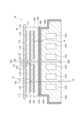
図1には、基板Wを吸着保持した状態の静電チャック10の構成が、模式的な断面図として示されている。静電チャック10は、誘電体基板100と、ベースプレート200と、接合層300と、を備える。Figure 1 shows a schematic cross-sectional view of the configuration of an
誘電体基板100は、セラミック焼結体からなる略円盤状の部材である。誘電体基板100は、例えば高純度の酸化アルミニウム(Al2O3)を含むが、他の材料を含んでもよい。誘電体基板100におけるセラミックスの純度や種類、添加物等は、半導体製造装置において誘電体基板100に求められる耐プラズマ性等を考慮して、適宜設定することができる。 The
誘電体基板100のうち図1における上方側の面110は、被吸着物である基板Wが載置される「載置面」となっている。また、誘電体基板100のうち図1における下方側の面120は、後述の接合層300を介してベースプレート200に接合される「被接合面」となっている。面110に対し垂直な方向に沿って、面110側から静電チャック10を見た場合の視点のことを、以下では「上面視」のようにも表記する。The
誘電体基板100の内部には吸着電極130が埋め込まれている。吸着電極130は、例えばタングステン等の金属材料により形成された薄い平板状の層であり、面110に対し平行となるように配置されている。吸着電極130の材料としては、タングステンの他、モリブデン、白金、パラジウム等を用いてもよい。給電路13を介して外部から吸着電極130に電圧が印加されると、面110と基板Wとの間に静電力が生じ、これにより基板Wが吸着保持される。吸着電極130は、所謂「単極」の電極として本実施形態のように1つだけ設けられていてもよいが、所謂「双極」の電極として2つ設けられていてもよい。An
図1においては、給電路13の全体が簡略化して描かれている。給電路13のうち誘電体基板100の内部の部分は、例えば、導電体の充填された細長いビア(穴)として構成されており、その下端には不図示の電極端子が設けられている。給電路13のうちベースプレート200を貫いている部分は、上記の電極端子に一端が接続された導電性の金属部材(例えばバスバー)である。ベースプレート200には、当該金属を挿通するための不図示の貫通穴が形成されている。当該貫通穴の内面と給電路13との間には、例えば円筒状の絶縁部材が設けられていてもよい。1, the entire
誘電体基板100の内部には、上記の吸着電極130に加えて、RF電極140も埋め込まれている。RF電極140は、半導体製造装置においてプラズマを発生させるための一対の対向電極のうちの1つ、として設けられている。対向電極のうちのもう一つは、半導体製造装置において静電チャック10よりも上方側となる位置に設けられる。これらの対向電極の間に高周波の交流電圧が印加されると、基板Wの上方側においてプラズマが発生し、基板Wに対する成膜やエッチング等の処理に供される。In addition to the above-mentioned
RF電極140は、吸着電極130と同様に、例えばタングステン等の金属材料により形成された薄い平板状の層である。RF電極140の材料としては、タングステンの他、モリブデン、白金、パラジウム等を用いてもよい。RF電極140は、吸着電極130よりも面120側となる位置に埋め込まれている。換言すれば、吸着電極130は、RF電極140よりも面110側となる位置に埋め込まれている。RF電極140は、吸着電極130と同様に、面110や吸着電極130に対して平行となるように配置されている。RF電極140は、上面視において略円形の単一の電極である。The
RF電極140のうち、上面視で給電路13と重なる分には、開口143が形成されている。開口143を形成しておくことにより、給電路13とRF電極140との間の絶縁が確保されている。An
図1に示されるように、RF電極140には給電路14が接続されている。給電路14は、RF電極140ともう一方の対向電極との間に高周波の交流電圧を印加する際に、RF電極140の電位をベースプレート200の電位と一致させるために設けられた電路である。図1においては、給電路14の全体が簡略化して描かれている。給電路14は、例えば、一端がRF電極140に繋がっており、他端が面120から下方に向けて突出するように形成された電極端子として構成される。給電路14のうち上記のように突出している部分は、ベースプレート200の面120に形成された不図示の凹部に埋め込まれており、ベースプレート200の金属部分に対して繋がっている。As shown in FIG. 1, the
誘電体基板100と基板Wとの間には空間SPが形成されている。半導体製造装置において成膜等の処理が行われる際には、空間SPには、後述のガス穴150を介して外部から温度調整用のヘリウムガスが供給される。誘電体基板100と基板Wとの間にヘリウムガスを介在させることで、両者間の熱抵抗が調整され、これにより基板Wの温度が適温に保たれる。尚、空間SPに供給される温度調整用のガスは、ヘリウムとは異なる種類のガスであってもよい。A space SP is formed between the
吸着面である面110上にはシールリング111やドット112が設けられており、空間SPはこれらの周囲に形成されている。A
シールリング111は、最外周となる位置において空間SPを区画する壁である。シールリング111の上端は面110の一部となっており、基板Wに当接する。尚、空間SPを分割するように複数のシールリング111が設けられていてもよい。このような構成とすることで、それぞれの空間SPにおけるヘリウムガスの圧力を個別に調整し、処理中における基板Wの表面温度分布を均一に近づけることが可能となる。The
図1等において符号「116」が付されている部分は、空間SPの底面である。以下では、当該部分のことを「底面116」とも称する。シールリング111は、次に述べるドット112と共に、面110の一部を底面116の位置まで掘り下げた結果として形成されている。The portion marked with the reference symbol "116" in FIG. 1 and other figures is the bottom surface of the space SP. Hereinafter, this portion will also be referred to as the "
ドット112は、底面116から突出する円形の突起である。ドット112は複数設けられており、誘電体基板100の吸着面において略均等に分散配置されている。それぞれのドット112の上端は、面110の一部となっており、基板Wに当接する。このようなドット112を複数設けておくことで、基板Wの撓みが抑制される。The
空間SPの底面116には、溝113が形成されている。溝113は、底面116から更に面120側へと後退させるように形成された溝である。溝113は、ガス穴150から供給されるヘリウムガスを、空間SP内に素早く拡散させ、空間SP内の圧力分布を短時間のうちに略均一とすることを目的として形成されている。A
誘電体基板100には、面120から面110側に向かって垂直に伸びるガス穴150が形成されており、当該ガス穴150が、図2に示される貫通穴151を介して空間SPに繋がっている。ガス穴150は複数個形成されているが、図1においてはそのうちの1つのみが図示されている。The
ベースプレート200は、誘電体基板100を支持する略円盤状の部材である。ベースプレート200は、例えばアルミニウムのような金属により形成されている。ベースプレート200のうち、図1における上方側の面210は、接合層300を介して誘電体基板100に接合される「被接合面」となっている。The
ベースプレート200のうち、図1における下方側の面220を除く表面の略全体には、絶縁膜230が形成されている。絶縁膜230は、例えばアルミナのような絶縁性の材料からなる膜であり、例えば溶射によって形成されている。先に述べた面210は、その全体が絶縁膜230上の面となっている。尚、ベースプレート200のうち絶縁膜230が形成されている範囲は、図1の例とは異なる範囲であってもよい。例えば、被接合面である面210の範囲のみに絶縁膜230が形成されていてもよい。An insulating
ベースプレート200の内部には、冷媒を流すための冷媒流路270が形成されている。半導体製造装置において成膜等の処理が行われる際には、外部から冷媒が冷媒流路270に供給され、これによりベースプレート200が冷却される。処理中において基板Wで生じた熱は、空間SPのヘリウムガス、誘電体基板100、及びベースプレート200を介して冷媒へと伝えられ、冷媒と共に外部へと排出される。A
ベースプレート200には、面210から面220側に向かって垂直に伸びるガス穴250が形成されている。ガス穴250は、上面視において誘電体基板100のガス穴150と重なる位置、のそれぞれに形成されており、接合層300に設けられた貫通穴を介してガス穴150に連通されている。ガス穴250は、誘電体基板100のガス穴150と共に、空間SPに向けてヘリウムガスを供給するための経路の一部となっている。Gas holes 250 are formed in the
尚、ガス穴250は、本実施形態のように全体が直線状に伸びるように形成されていてもよいが、面220に向かう途中で屈曲するように形成されていてもよい。また、面210側の複数のガス穴250を、ベースプレート200の内部において少数の流路に集約した上で、当該流路を面220側まで伸ばすような構成としてもよい。The gas holes 250 may be formed so as to extend linearly as in this embodiment, but may also be formed so as to bend on the way to the
接合層300は、誘電体基板100とベースプレート200との間に設けられた層であって、両者を接合している。接合層300は、絶縁性の材料からなる接着材を硬化させたものである。このような接着剤としては、例えばシリコーン系の接着剤を用いることができる。The
ガス穴150の上端部やその近傍部分の具体的な構成について説明する。図2には、当該部分の構成が模式的な断面図として示されている。同図に示されるように、ガス穴150は、溝113の直下となる位置において、面120から溝113に向かって伸びるように形成されているのであるが、溝113の底面までは到達していない。ガス穴150と空間SPとの間は貫通穴151によって連通されている。The specific configuration of the upper end of the
貫通穴151は、ガス穴150の上端から溝113の底面まで、直線状に伸びるように形成された円形の貫通穴である。貫通穴151の半径は、ガス穴150の半径よりも小さい。また、貫通穴151の中心軸AXは、ガス穴150の中心軸と一致している。つまり、貫通穴151は、面110に対し垂直な方向に伸びている。ガス穴150を通ったヘリウムガスは、貫通穴151から空間SPへと供給される。貫通穴151は、貫通穴であるガス穴150のうち最も面110側の部分、すなわち、ガスの出口部分ということもできる。The through
上記のように、ガス穴150のうちガスの出口部分の半径を小さくしておくことで、ガス穴150を通じた絶縁破壊の発生を生じにくくすることができる。このような態様に換えて、ガス穴150が、そのまま溝113の底面まで伸びているような態様であってもよい。As described above, by making the radius of the gas outlet portion of the
図2に示されるように、ガス穴150の内部には、多孔質プラグ155が配置されている。多孔質プラグ155は、通気性を有する多孔質部材により形成された略円柱形状の部材である。多孔質プラグ155の上端と、ガス穴150の上端との間には、空間PNが形成されている。多孔質プラグ155の配置によって、基板Wとベースプレート200との間における絶縁破壊の発生を、更に生じにくくすることができる。これと同様に、ガス穴250のうち接合層300の近傍となる部分にも、絶縁破壊を防止するための多孔質プラグが配置されていてもよい。2, a
吸着電極130のうち、上面視で貫通穴151やガス穴150と重なる部分には、開口131が形成されている。上面視において、開口131は円形の開口であり、その中心は中心軸AXの上にある。また、開口131の半径R1は貫通穴151の半径R0よりも大きい。つまり、開口131は、上面視において貫通穴151と同心であり、且つ貫通穴151を包含する円形の開口となっている。尚、貫通穴151の半径R0は、例えば0.15mmもしくはそれ以下である。An
RF電極140のうち、上面視で貫通穴151やガス穴150と重なる部分には、開口141が形成されている。上面視において、開口141は円形の開口であり、その中心は中心軸AXの上にある。また、開口141の半径R2は貫通穴151の半径R0よりも大きい。つまり、開口141は、上面視において貫通穴151と同心であり、且つ貫通穴151を包含する円形の開口となっている。本実施形態では、開口141の半径R2が開口131の半径R1よりも大きい。An
開口131や開口141が形成されていることで、貫通穴151の内面において、吸着電極130やRF電極140が露出してしまうことが防止されている。The formation of the
本実施形態では、開口141の半径R2が十分に大きくなっており、具体的には1.75mm以上となっている。In this embodiment, the radius R2 of the
このような構成としたことの理由について説明する。図3(B)には、比較例に係る静電チャックのうち、図2と対応する部分の構成が示されている。この比較例では、開口141の半径R2が、開口131の半径R1と同程度に小さくなっている。。The reason for this configuration will be explained below. FIG. 3B shows the configuration of a portion of an electrostatic chuck according to a comparative example that corresponds to FIG. 2. In this comparative example, the radius R2 of the
基板Wの処理中においては、吸着電極130は高電位となる一方で、RF電極140は所定の低い電位(ベースプレート200と同じ電位であって、例えば接地電位)に保たれる。図3(B)に示される各矢印は、開口141や開口131の縁近傍における電気力線を模式的に表している。図3(B)では、それぞれの電気力線は、開口131の縁から開口141の縁に向かって伸びている。尚、開口131の大きさによっては、開口141の縁に向かう電気力線は、処理中の基板Wから伸びている場合もある。During processing of the substrate W, the chucking
この比較例のように、開口141の半径R2が比較的小さくなっている場合には、貫通穴151における電界の方向(つまり、上記電気力線の方向)は、貫通穴151の伸びる方向と概ね同じになる。このため、この比較例の構成においては、貫通穴151を通じた経路で絶縁破壊が起こってしまう可能性がある。When the radius R2 of the
そこで、本実施形態に係る静電チャック10では、半径R2を十分に大きくすることで上記のような絶縁破壊を防止している。Therefore, in the
図3(A)では、図2と同じ本実施形態の断面に、図3(B)と同様に電気力線を示す矢印を表してある。本実施形態では、開口141の半径R2を大きくしたことで、開口141の縁が貫通穴151から遠ざかっている。その結果、貫通穴151においては、高電位の部分から開口141の縁に向かう電界のうち、貫通穴151の伸びる方向に沿った成分が小さくなる。「高電位の部分」とは、例えば吸着電極130であるが、処理中の基板Wである場合もある。In FIG. 3(A), the cross section of this embodiment is the same as in FIG. 2, but arrows indicating electric field lines are shown in the same manner as in FIG. 3(B). In this embodiment, the radius R2 of the
図3(A)の本実施形態においては、開口141に向かう電界のうち、貫通穴151の伸びる方向に沿った成分が小さくなるので、貫通穴151を通じて絶縁破壊が生じる可能性を従来よりも低く抑えることが可能となっている。In the present embodiment shown in FIG. 3(A), the component of the electric field directed toward the
本発明者らが実験等により確認したところによれば、半径R2を1.75mm以上としておけば、貫通穴151を通じた絶縁破壊の発生を十分に防止できるという知見が得られている。The inventors have confirmed through experiments and other means that if the radius R2 is set to 1.75 mm or greater, it is possible to sufficiently prevent dielectric breakdown through the through
尚、半径R2を1.75mm以上としたことによる上記の効果は、半径R2と半径R1とが互いに同一の場合でも、ある程度奏することが確認されている。つまり、半径R2だけでなく半径R1をも大きくした場合であっても、貫通穴151を通じた絶縁破壊の発生を防止することができる。ただし、吸着電極130の開口131を大きくし過ぎると、吸着力が不足して、基板Wの保持が十分には行われなくなってしまう恐れがある。このため、本実施形態のように、RF電極140の開口141のみを大きくすることが好ましい。It has been confirmed that the above-mentioned effect of setting the radius R2 to 1.75 mm or more is achieved to some extent even when the radius R2 and the radius R1 are the same. In other words, even when not only the radius R2 but also the radius R1 are increased, it is possible to prevent the occurrence of dielectric breakdown through the through-
開口141の半径R2を大きくするほど、貫通穴151において絶縁破壊が生じる可能性は低くなる。図4(B)には、半径R2を極端に大きくした場合の比較例が示されている。図4(A)は、図3(A)と同じ本実施形態を表している。The larger the radius R2 of the
図4(B)の比較例のように、半径R2を大きくし過ぎた場合には、高電位となっている部分(この例では吸着電極130)から伸びる電気力線の一部が、開口141を通じて下方側の部分にまで影響を与えてしまうことがある。例えば、図4(B)において矢印AR1で示される電気力線は、RF電極140によって遮蔽されることなく、接合層300の近傍部分にも電位差を生じさせる。その結果、接合層300に形成された貫通穴の内面(図4(B)において符号「301」が付されている部分)に沿った絶縁破壊を生じさせてしまう可能性がある。As in the comparative example of FIG. 4B, if the radius R2 is made too large, some of the electric field lines extending from the part with high potential (the chucking
本発明者らが実験等により確認したところによれば、半径R2を5.35mm以下とすれば、このような絶縁破壊の発生を十分に防止できるという知見が得られている。このため、半径R2を大きくし過ぎることなく、5.35mm以下としておくことが好ましい。The inventors have confirmed through experiments that if the radius R2 is 5.35 mm or less, the occurrence of such dielectric breakdown can be sufficiently prevented. For this reason, it is preferable to keep the radius R2 at 5.35 mm or less, without making it too large.
半径R2と半径R0との差は、1.6mm以上であり且つ5.4mm以下の範囲内であることが好ましい。また、本実施形態のように、半径R2を半径R1よりも大きくする場合には、半径R2と半径R1との差を2.7mm以下とすることが好ましい。It is preferable that the difference between radius R2 and radius R0 is in the range of 1.6 mm or more and 5.4 mm or less. Furthermore, when radius R2 is made larger than radius R1 as in this embodiment, it is preferable that the difference between radius R2 and radius R1 is 2.7 mm or less.
以上のような開口141や開口131は、誘電体基板100のうち、貫通穴151とは別の目的で設けられた貫通穴と上面視で重なる位置に形成してもよい。例えば、誘電体基板100には、半導体製造装置に設けられた不図示のリフトピンを挿通するためのリフトピン穴、が形成されることもある。上面視でリフトピン穴と重なる位置のそれぞれに、本実施形態と同様の開口141や開口131を形成しても、以上で説明したものと同様の効果を奏することができる。The
ただし、ガス供給用の穴である貫通穴151においては、その内側の圧力は、絶縁破壊が比較的生じやすい圧力域となる傾向がある。このため、貫通穴151の位置においては、上記のような開口141や開口131の形状を適用することの効果が特に大きい。However, the pressure inside the through
以上、具体例を参照しつつ本実施形態について説明した。しかし、本開示はこれらの具体例に限定されるものではない。これら具体例に、当業者が適宜設計変更を加えたものも、本開示の特徴を備えている限り、本開示の範囲に包含される。前述した各具体例が備える各要素およびその配置、条件、形状などは、例示したものに限定されるわけではなく適宜変更することができる。前述した各具体例が備える各要素は、技術的な矛盾が生じない限り、適宜組み合わせを変えることができる。The present embodiment has been described above with reference to specific examples. However, the present disclosure is not limited to these specific examples. Design modifications to these specific examples made by a person skilled in the art are also included within the scope of the present disclosure as long as they have the features of the present disclosure. The elements of each of the above-mentioned specific examples, as well as their arrangement, conditions, shape, etc., are not limited to those exemplified and can be modified as appropriate. The elements of each of the above-mentioned specific examples can be combined in different ways as appropriate, as long as no technical contradictions arise.
W:基板
10:静電チャック
100:誘電体基板
110:面
140:RF電極
141:開口
151:貫通穴 W: Substrate 10: Electrostatic chuck 100: Dielectric substrate 110: Surface 140: RF electrode 141: Opening 151: Through hole
Claims (3)
Translated fromJapanese前記誘電体基板の内部に埋め込まれた吸着電極と、
前記吸着電極とは異なる位置において、前記誘電体基板の内部に埋め込まれたRF電極と、を備え、
前記RF電極には、前記貫通穴と同心であり且つ前記貫通穴を包含する円形の開口が形成されており、
前記開口の半径が1.75mm以上であることを特徴とする静電チャック。 a dielectric substrate having a mounting surface on which an object to be attached is placed and having a through hole formed perpendicular to the mounting surface;
an adsorption electrode embedded inside the dielectric substrate;
an RF electrode embedded in the dielectric substrateat a position different from the chucking electrode ;
The RF electrode has a circular opening formed therein that is concentric with and encompasses the through hole;
The opening has a radius of 1.75 mm or more.
Priority Applications (5)
| Application Number | Priority Date | Filing Date | Title |
|---|---|---|---|
| JP2023049641AJP7494973B1 (en) | 2023-03-27 | 2023-03-27 | Electrostatic Chuck |
| KR1020240015739AKR20240145386A (en) | 2023-03-27 | 2024-02-01 | Electrostatic chuck |
| CN202410172197.0ACN118712115A (en) | 2023-03-27 | 2024-02-07 | Electrostatic chuck |
| TW113105881ATW202439372A (en) | 2023-03-27 | 2024-02-20 | Electrostatic suction cup |
| US18/610,491US20240331985A1 (en) | 2023-03-27 | 2024-03-20 | Electrostatic chuck |
Applications Claiming Priority (1)
| Application Number | Priority Date | Filing Date | Title |
|---|---|---|---|
| JP2023049641AJP7494973B1 (en) | 2023-03-27 | 2023-03-27 | Electrostatic Chuck |
Publications (2)
| Publication Number | Publication Date |
|---|---|
| JP7494973B1true JP7494973B1 (en) | 2024-06-04 |
| JP2024138919A JP2024138919A (en) | 2024-10-09 |
Family
ID=91321925
Family Applications (1)
| Application Number | Title | Priority Date | Filing Date |
|---|---|---|---|
| JP2023049641AActiveJP7494973B1 (en) | 2023-03-27 | 2023-03-27 | Electrostatic Chuck |
Country Status (2)
| Country | Link |
|---|---|
| JP (1) | JP7494973B1 (en) |
| CN (1) | CN118712115A (en) |
Citations (7)
| Publication number | Priority date | Publication date | Assignee | Title |
|---|---|---|---|---|
| JP2000349141A (en) | 1999-06-09 | 2000-12-15 | Mitsubishi Electric Corp | Plasma processing equipment |
| JP2006128203A (en) | 2004-10-26 | 2006-05-18 | Kyocera Corp | Wafer support member and semiconductor manufacturing apparatus using the same |
| JP2009218592A (en) | 2008-03-11 | 2009-09-24 | Ngk Insulators Ltd | Electrostatic chuck |
| JP3154629U (en) | 2009-08-04 | 2009-10-22 | 日本碍子株式会社 | Electrostatic chuck |
| WO2017126534A1 (en) | 2016-01-19 | 2017-07-27 | 住友大阪セメント株式会社 | Electrostatic chuck device |
| WO2020153449A1 (en) | 2019-01-24 | 2020-07-30 | 京セラ株式会社 | Electrostatic chuck |
| JP2021040109A (en) | 2019-09-05 | 2021-03-11 | Toto株式会社 | Electrostatic chuck |
Family Cites Families (1)
| Publication number | Priority date | Publication date | Assignee | Title |
|---|---|---|---|---|
| JP3457477B2 (en)* | 1995-09-06 | 2003-10-20 | 日本碍子株式会社 | Electrostatic chuck |
- 2023
- 2023-03-27JPJP2023049641Apatent/JP7494973B1/enactiveActive
- 2024
- 2024-02-07CNCN202410172197.0Apatent/CN118712115A/enactivePending
Patent Citations (7)
| Publication number | Priority date | Publication date | Assignee | Title |
|---|---|---|---|---|
| JP2000349141A (en) | 1999-06-09 | 2000-12-15 | Mitsubishi Electric Corp | Plasma processing equipment |
| JP2006128203A (en) | 2004-10-26 | 2006-05-18 | Kyocera Corp | Wafer support member and semiconductor manufacturing apparatus using the same |
| JP2009218592A (en) | 2008-03-11 | 2009-09-24 | Ngk Insulators Ltd | Electrostatic chuck |
| JP3154629U (en) | 2009-08-04 | 2009-10-22 | 日本碍子株式会社 | Electrostatic chuck |
| WO2017126534A1 (en) | 2016-01-19 | 2017-07-27 | 住友大阪セメント株式会社 | Electrostatic chuck device |
| WO2020153449A1 (en) | 2019-01-24 | 2020-07-30 | 京セラ株式会社 | Electrostatic chuck |
| JP2021040109A (en) | 2019-09-05 | 2021-03-11 | Toto株式会社 | Electrostatic chuck |
Also Published As
| Publication number | Publication date |
|---|---|
| CN118712115A (en) | 2024-09-27 |
| JP2024138919A (en) | 2024-10-09 |
Similar Documents
| Publication | Publication Date | Title |
|---|---|---|
| JP7494973B1 (en) | Electrostatic Chuck | |
| JP2025144847A (en) | Electrostatic chuck | |
| JP2024139669A (en) | Electrostatic Chuck | |
| JP7675124B2 (en) | Electrostatic Chuck | |
| JP7709480B2 (en) | Electrostatic Chuck | |
| JP7343069B1 (en) | electrostatic chuck | |
| JP7494972B1 (en) | Electrostatic Chuck | |
| JP7670191B1 (en) | Electrostatic Chuck | |
| JP7697548B1 (en) | Electrostatic Chuck | |
| KR20240145386A (en) | Electrostatic chuck | |
| JP7658477B1 (en) | Electrostatic Chuck | |
| JP7639953B1 (en) | Electrostatic Chuck | |
| JP2025146828A (en) | Electrostatic chuck | |
| JP2025144846A (en) | Electrostatic chuck | |
| JP7747092B2 (en) | Electrostatic chuck | |
| JP2024175418A (en) | Electrostatic Chuck | |
| JP2025084481A (en) | Electrostatic Chuck | |
| JP2024139692A (en) | Electrostatic Chuck | |
| JP2025113555A (en) | Electrostatic chuck | |
| JP2024175417A (en) | Electrostatic Chuck | |
| JP2024175420A (en) | Electrostatic Chuck | |
| JP2025080476A (en) | Electrostatic Chuck | |
| JP2025112084A (en) | holding device | |
| JP2025050250A (en) | Electrostatic Chuck | |
| JP2025131339A (en) | Electrostatic chuck |
Legal Events
| Date | Code | Title | Description |
|---|---|---|---|
| A621 | Written request for application examination | Free format text:JAPANESE INTERMEDIATE CODE: A621 Effective date:20230530 | |
| A871 | Explanation of circumstances concerning accelerated examination | Free format text:JAPANESE INTERMEDIATE CODE: A871 Effective date:20230530 | |
| A131 | Notification of reasons for refusal | Free format text:JAPANESE INTERMEDIATE CODE: A131 Effective date:20230808 | |
| A131 | Notification of reasons for refusal | Free format text:JAPANESE INTERMEDIATE CODE: A131 Effective date:20231226 | |
| A521 | Request for written amendment filed | Free format text:JAPANESE INTERMEDIATE CODE: A523 Effective date:20240206 | |
| TRDD | Decision of grant or rejection written | ||
| A01 | Written decision to grant a patent or to grant a registration (utility model) | Free format text:JAPANESE INTERMEDIATE CODE: A01 Effective date:20240423 | |
| A61 | First payment of annual fees (during grant procedure) | Free format text:JAPANESE INTERMEDIATE CODE: A61 Effective date:20240506 | |
| R150 | Certificate of patent or registration of utility model | Ref document number:7494973 Country of ref document:JP Free format text:JAPANESE INTERMEDIATE CODE: R150 | |
| R157 | Certificate of patent or utility model (correction) | Free format text:JAPANESE INTERMEDIATE CODE: R157 |