JP7489509B2 - Semiconductor Device - Google Patents
Semiconductor DeviceDownload PDFInfo
- Publication number
- JP7489509B2 JP7489509B2JP2023028593AJP2023028593AJP7489509B2JP 7489509 B2JP7489509 B2JP 7489509B2JP 2023028593 AJP2023028593 AJP 2023028593AJP 2023028593 AJP2023028593 AJP 2023028593AJP 7489509 B2JP7489509 B2JP 7489509B2
- Authority
- JP
- Japan
- Prior art keywords
- film
- oxide semiconductor
- semiconductor film
- transistor
- oxide
- Prior art date
- Legal status (The legal status is an assumption and is not a legal conclusion. Google has not performed a legal analysis and makes no representation as to the accuracy of the status listed.)
- Active
Links
Images


Classifications
- H—ELECTRICITY
- H10—SEMICONDUCTOR DEVICES; ELECTRIC SOLID-STATE DEVICES NOT OTHERWISE PROVIDED FOR
- H10D—INORGANIC ELECTRIC SEMICONDUCTOR DEVICES
- H10D62/00—Semiconductor bodies, or regions thereof, of devices having potential barriers
- H10D62/40—Crystalline structures
- H—ELECTRICITY
- H10—SEMICONDUCTOR DEVICES; ELECTRIC SOLID-STATE DEVICES NOT OTHERWISE PROVIDED FOR
- H10D—INORGANIC ELECTRIC SEMICONDUCTOR DEVICES
- H10D30/00—Field-effect transistors [FET]
- H10D30/01—Manufacture or treatment
- H10D30/021—Manufacture or treatment of FETs having insulated gates [IGFET]
- H10D30/031—Manufacture or treatment of FETs having insulated gates [IGFET] of thin-film transistors [TFT]
- H—ELECTRICITY
- H10—SEMICONDUCTOR DEVICES; ELECTRIC SOLID-STATE DEVICES NOT OTHERWISE PROVIDED FOR
- H10D—INORGANIC ELECTRIC SEMICONDUCTOR DEVICES
- H10D30/00—Field-effect transistors [FET]
- H10D30/60—Insulated-gate field-effect transistors [IGFET]
- H10D30/67—Thin-film transistors [TFT]
- H10D30/674—Thin-film transistors [TFT] characterised by the active materials
- H10D30/6755—Oxide semiconductors, e.g. zinc oxide, copper aluminium oxide or cadmium stannate
- H—ELECTRICITY
- H10—SEMICONDUCTOR DEVICES; ELECTRIC SOLID-STATE DEVICES NOT OTHERWISE PROVIDED FOR
- H10D—INORGANIC ELECTRIC SEMICONDUCTOR DEVICES
- H10D86/00—Integrated devices formed in or on insulating or conducting substrates, e.g. formed in silicon-on-insulator [SOI] substrates or on stainless steel or glass substrates
- H10D86/40—Integrated devices formed in or on insulating or conducting substrates, e.g. formed in silicon-on-insulator [SOI] substrates or on stainless steel or glass substrates characterised by multiple TFTs
- H10D86/421—Integrated devices formed in or on insulating or conducting substrates, e.g. formed in silicon-on-insulator [SOI] substrates or on stainless steel or glass substrates characterised by multiple TFTs having a particular composition, shape or crystalline structure of the active layer
- H10D86/423—Integrated devices formed in or on insulating or conducting substrates, e.g. formed in silicon-on-insulator [SOI] substrates or on stainless steel or glass substrates characterised by multiple TFTs having a particular composition, shape or crystalline structure of the active layer comprising semiconductor materials not belonging to the Group IV, e.g. InGaZnO
- H—ELECTRICITY
- H10—SEMICONDUCTOR DEVICES; ELECTRIC SOLID-STATE DEVICES NOT OTHERWISE PROVIDED FOR
- H10D—INORGANIC ELECTRIC SEMICONDUCTOR DEVICES
- H10D86/00—Integrated devices formed in or on insulating or conducting substrates, e.g. formed in silicon-on-insulator [SOI] substrates or on stainless steel or glass substrates
- H10D86/40—Integrated devices formed in or on insulating or conducting substrates, e.g. formed in silicon-on-insulator [SOI] substrates or on stainless steel or glass substrates characterised by multiple TFTs
- H10D86/60—Integrated devices formed in or on insulating or conducting substrates, e.g. formed in silicon-on-insulator [SOI] substrates or on stainless steel or glass substrates characterised by multiple TFTs wherein the TFTs are in active matrices
- H—ELECTRICITY
- H10—SEMICONDUCTOR DEVICES; ELECTRIC SOLID-STATE DEVICES NOT OTHERWISE PROVIDED FOR
- H10D—INORGANIC ELECTRIC SEMICONDUCTOR DEVICES
- H10D99/00—Subject matter not provided for in other groups of this subclass
Landscapes
- Thin Film Transistor (AREA)
- Electroluminescent Light Sources (AREA)
- Liquid Crystal (AREA)
- Chemical & Material Sciences (AREA)
- Crystallography & Structural Chemistry (AREA)
- Physical Deposition Of Substances That Are Components Of Semiconductor Devices (AREA)
- Drying Of Semiconductors (AREA)
Description
Translated fromJapanese酸化物半導体を用いる半導体装置の作製方法に関する。This relates to a method for manufacturing a semiconductor device using an oxide semiconductor.
電界効果トランジスタの一つである薄膜トランジスタ(TFT)は、絶縁表面上に形成さ
れた厚さ数~数百nm程度の半導体膜を活性層として用いており、液晶表示装置、発光装
置などのフラットパネルディスプレイや、ICなどの電子デバイスに広く応用されている
。Thin film transistors (TFTs), a type of field effect transistor, use a semiconductor film with a thickness of several to several hundred nanometers formed on an insulating surface as an active layer, and are widely used in flat panel displays such as liquid crystal display devices and light-emitting devices, as well as electronic devices such as ICs.
近年では、シリコンやゲルマニウムのみならず、金属酸化物を活性層として用いるトラン
ジスタの開発が行われている。金属酸化物は様々な用途に用いられており、例えば、よく
知られた金属酸化物である酸化インジウムは、液晶表示装置などで透明電極材料として用
いられている。そして、金属酸化物の中には半導体特性を示すものがあり、酸化物半導体
と呼ばれている。半導体特性を示す金属酸化物としては、例えば、酸化タングステン、酸
化錫、酸化インジウム、酸化亜鉛などがあり、このような半導体特性を示す金属酸化物を
チャネル形成領域に用いるトランジスタが、既に知られている(特許文献1乃至4、非特
許文献1)。In recent years, transistors using metal oxides as active layers, in addition to silicon and germanium, have been developed. Metal oxides are used for various purposes. For example, indium oxide, a well-known metal oxide, is used as a transparent electrode material in liquid crystal display devices and the like. Some metal oxides exhibit semiconducting properties and are called oxide semiconductors. Examples of metal oxides that exhibit semiconducting properties include tungsten oxide, tin oxide, indium oxide, and zinc oxide, and transistors that use such metal oxides that exhibit semiconducting properties in a channel formation region are already known (
ところで、金属酸化物は一元系酸化物のみでなく多元系酸化物も知られている。例えば、
ホモロガス相を有するInGaO3(ZnO)m(m:自然数)は、In、Ga及びZn
を有する多元系酸化物半導体として知られている(非特許文献2乃至4)。そして、上記
のようなIn-Ga-Zn系酸化物で構成される酸化物半導体をトランジスタのチャネル
層に適用可能であることが確認されている(特許文献5、非特許文献5及び6)。Incidentally, metal oxides include not only single-component oxides but also multi-component oxides. For example,
InGaO3 (ZnO)m (m: natural number) having a homologous phase is a compound of In, Ga, and Zn.
(
安定した電気特性を有するトランジスタを有する、信頼性のよい半導体装置を作製するた
めの、半導体装置の作製方法を提供することを課題の一とする。An object of the present invention is to provide a method for manufacturing a semiconductor device in order to manufacture a reliable semiconductor device including a transistor with stable electrical characteristics.
酸化物半導体をチャネル形成領域に用いたトランジスタを有する半導体装置の作製におい
て、酸化物半導体膜内の水分などの極性分子を含む不純物を低減し、酸化物半導体膜の純
度を高めるために、マイクロ波、高周波などの電磁波の照射を行う。また、酸化物半導体
膜中だけでなく、ゲート絶縁膜内に存在する水分などの不純物を低減する、または、酸化
物半導体膜の上下に接する膜と酸化物半導体膜の界面に存在する水分などの不純物を低減
するために、電磁波の照射を行う。In manufacturing a semiconductor device including a transistor in which an oxide semiconductor is used for a channel formation region, the oxide semiconductor film is irradiated with electromagnetic waves such as microwaves or high frequency waves in order to reduce impurities including polar molecules such as moisture in the oxide semiconductor film and to increase the purity of the oxide semiconductor film. In addition, the oxide semiconductor film is irradiated with electromagnetic waves in order to reduce impurities such as moisture present not only in the oxide semiconductor film but also in a gate insulating film or to reduce impurities such as moisture present at interfaces between the oxide semiconductor film and films in contact with the top and bottom of the oxide semiconductor film.
具体的には、水分などの不純物を低減するため、酸化物半導体膜を形成後、酸化物半導体
膜が露出した状態で窒素、または希ガス(アルゴン、ヘリウムなど)の不活性気体雰囲気
下、或いは減圧下で、水に吸収されやすい周波数の電磁波(マイクロ波だと周波数300
MHz以上3THz以下、高周波だと周波数1MHz以上300MHz以下)を、酸化物
半導体膜に照射することで、酸化物半導体膜が含有する水分を低減する。なお、酸化物半
導体膜には水素、OHも含まれているので、これらも電磁波の照射により酸化物半導体膜
から脱離すると考えられる。Specifically, in order to reduce impurities such as moisture, after an oxide semiconductor film is formed, electromagnetic waves having a frequency that is easily absorbed by water (a frequency of 300 nm for microwaves) are irradiated under an inert gas atmosphere of nitrogen or a rare gas (such as argon or helium) or under reduced pressure while the oxide semiconductor film is exposed.
The oxide semiconductor film is irradiated with electromagnetic waves having a frequency of from 1 MHz to 3 THz, or from 1 MHz to 300 MHz in the case of a high frequency, to thereby reduce moisture contained in the oxide semiconductor film. Note that the oxide semiconductor film also contains hydrogen and OH, which are considered to be released from the oxide semiconductor film by irradiation with electromagnetic waves.
酸化物半導体膜への電磁波の照射は、加熱処理と並行して行うようにしても良い。電磁波
の照射を加熱処理と並行して行うことで、酸化物半導体膜中の水分などの不純物を短い時
間でより効率よく低減することができる。ただし、加熱処理は、酸化物半導体を構成して
いるZnなどの融点の低い金属が気化しにくい温度、例えば100℃以上350℃未満、
好ましくは150℃以上250℃未満で行う。なお、室温で酸化物半導体膜に電磁波を照
射したとしても、水分子が電磁波のエネルギーを吸収して振動を行うため、結果的に酸化
物半導体膜の温度は室温よりも高くなることが予想される。加熱処理を電磁波の照射と並
行して行う場合、電磁波の照射による温度上昇分を考慮して、酸化物半導体膜の温度を管
理することが望ましい。また、電磁波の照射と加熱処理を併用する場合、加熱処理の設定
温度まで酸化物半導体膜の温度を上昇させてから、電磁波の照射を行い、その後、室温以
上100℃未満の範囲まで酸化物半導体膜を徐冷する。The oxide semiconductor film may be irradiated with electromagnetic waves in parallel with heat treatment. By irradiating with electromagnetic waves in parallel with heat treatment, impurities such as moisture in the oxide semiconductor film can be reduced more efficiently in a short time. Note that the heat treatment should be performed at a temperature at which a metal with a low melting point, such as Zn, which constitutes the oxide semiconductor, is unlikely to vaporize, for example, at 100° C. or higher and lower than 350° C.
The temperature is preferably 150° C. or higher and lower than 250° C. Even if the oxide semiconductor film is irradiated with electromagnetic waves at room temperature, water molecules absorb the energy of the electromagnetic waves and vibrate, so that the temperature of the oxide semiconductor film is expected to be higher than room temperature. When the heat treatment is performed in parallel with the electromagnetic wave irradiation, it is preferable to manage the temperature of the oxide semiconductor film in consideration of the temperature increase due to the electromagnetic wave irradiation. When the electromagnetic wave irradiation and the heat treatment are used in combination, the temperature of the oxide semiconductor film is increased to a set temperature for the heat treatment, and then the electromagnetic wave irradiation is performed, and the oxide semiconductor film is gradually cooled to a temperature range of room temperature or higher and lower than 100° C.
酸化物半導体膜内に存在する水分などの不純物の除去を加熱処理単独で短時間にて行うに
は、上記設定温度の範囲より高い温度になるよう酸化物半導体膜を加熱するのがより効果
的ではある。しかし本発明の一態様では、電磁波の照射を用いることで、上記設定温度、
もしくは上記設定温度よりも低い温度範囲であっても、水分などの不純物の効率的な除去
を短時間にて実現することができる。よって、水分などの不純物の除去を行う際に、融点
の低いZnなどの金属が気化して酸化物半導体の組成比に変化が生じるのを防ぐことがで
き、酸化物半導体で作製されるトランジスタの特性の劣化を防ぐことができる。In order to remove impurities such as moisture present in the oxide semiconductor film in a short time by heat treatment alone, it is more effective to heat the oxide semiconductor film to a temperature higher than the above-mentioned set temperature range.
Alternatively, even if the temperature range is lower than the above set temperature, impurities such as moisture can be efficiently removed in a short time. Therefore, when impurities such as moisture are removed, it is possible to prevent a change in the composition ratio of the oxide semiconductor caused by vaporization of a metal such as Zn having a low melting point, and it is possible to prevent deterioration of the characteristics of a transistor made of the oxide semiconductor.
電子供与体(ドナー)となる水分、水素、OHなどの不純物の脱離により高純度化された
酸化物半導体(purified OS)は、i型(真性半導体)又はi型に限りなく近
い。上記酸化物半導体をトランジスタに用いることで、閾値電圧の変動など、不純物によ
ってトランジスタの特性が劣化するのを防ぐことができ、信頼性が向上する。An oxide semiconductor (purified OS) that is highly purified by eliminating impurities such as moisture, hydrogen, and OH that serve as electron donors (donors) is an i-type (intrinsic semiconductor) or is very close to an i-type. By using such an oxide semiconductor in a transistor, deterioration of the characteristics of the transistor due to impurities, such as a shift in threshold voltage, can be prevented, and reliability can be improved.
さらに、酸化物半導体膜に電磁波の照射を行い、水分などの不純物の除去を行った後、酸
化物半導体膜に接するように酸化物絶縁膜の形成を行っても良い。上記構成により、電磁
波の照射、或いは電磁波の照射と並行して行った加熱処理により、酸化物半導体膜に酸素
欠損が発生していたとしても、酸化物半導体膜に酸素が供与される。そのため、酸化物半
導体膜の酸化物絶縁膜と接する領域において、ドナーとなる酸素欠損を低減し、化学量論
比を満たすことができる。その結果、酸化物半導体膜をi型化または実質的にi型化にす
ることができ、トランジスタの電気特性の向上および、電気特性のばらつきを軽減するこ
とができる。Furthermore, the oxide semiconductor film may be irradiated with electromagnetic waves to remove impurities such as moisture, and then an oxide insulating film may be formed in contact with the oxide semiconductor film. With the above structure, even if oxygen vacancies are generated in the oxide semiconductor film by irradiation with electromagnetic waves or heat treatment performed in parallel with the irradiation with electromagnetic waves, oxygen is provided to the oxide semiconductor film. Therefore, in a region of the oxide semiconductor film in contact with the oxide insulating film, oxygen vacancies serving as donors can be reduced and the stoichiometric ratio can be satisfied. As a result, the oxide semiconductor film can be made i-type or substantially i-type, and the electrical characteristics of the transistor can be improved and the variation in the electrical characteristics can be reduced.
具体的に、高純度化された酸化物半導体は、二次イオン質量分析法(SIMS:Seco
ndary Ion Mass Spectroscopy)による水素濃度の測定値が
、5×10¹⁹/cm3以下、好ましくは5×1018/cm3以下、より好ましくは5
×1017/cm3以下、さらに好ましくは1×1016/cm3未満とする。また、ホ
ール効果測定により測定できる酸化物半導体膜のキャリア密度は、1×10¹⁴/cm3
未満、好ましくは1×10¹²/cm3未満、さらに好ましくは1×1011/cm3未
満とする。また、酸化物半導体のバンドギャップは、2eV以上、好ましくは2.5eV
以上、より好ましくは3eV以上である。Specifically, the highly purified oxide semiconductor is analyzed by secondary ion mass spectrometry (SIMS).
The hydrogen concentration measured by undary ion mass spectroscopy is 5×10¹⁹ /cm3 or less, preferably 5×10¹⁸ /cm3 or less, and more preferably 5×10 18 /
The carrier density of the oxide semiconductor filmthat can be measured by Hall effect measurement is preferably 1×10 14/ cm3 or less, more preferably less than 1×10¹⁶ /cm3.
The band gap of the oxide semiconductor is2 eV or more, preferably2.5 eVormore .
It is preferably 3 eV or more.
ここで、酸化物半導体膜中の、水素濃度の分析について触れておく。酸化物半導体膜中及
び導電膜中の水素濃度測定は、二次イオン質量分析法(SIMS:Secondary
Ion Mass Spectroscopy)で行う。SIMS分析は、その原理上、
試料表面近傍や、材質が異なる膜との積層界面近傍のデータを正確に得ることが困難であ
ることが知られている。そこで、膜中における水素濃度の厚さ方向の分布をSIMSで分
析する場合、対象となる膜が存在する範囲において、値に極端な変動が無く、ほぼ一定の
値が得られる領域における平均値を、水素濃度として採用する。また、測定の対象となる
膜の厚さが小さい場合、隣接する膜内の水素濃度の影響を受けて、ほぼ一定の値が得られ
る領域を見いだせない場合がある。この場合、当該膜が存在する領域における、水素濃度
の最大値または最小値を、当該膜中の水素濃度として採用する。さらに、当該膜の存在す
る領域において、最大値を有する山型のピーク、最小値を有する谷型のピークが存在しな
い場合、変曲点の値を水素濃度として採用する。Here, the analysis of the hydrogen concentration in the oxide semiconductor film will be described. The hydrogen concentration in the oxide semiconductor film and the conductive film is measured by secondary ion mass spectrometry (SIMS).
The SIMS analysis is carried out by ion mass spectroscopy.
It is known that it is difficult to obtain accurate data near the sample surface or near the laminated interface with a film of a different material. Therefore, when analyzing the distribution of hydrogen concentration in the thickness direction in a film by SIMS, the average value in the region where the target film exists and where there is no extreme fluctuation in the value and an almost constant value is obtained is adopted as the hydrogen concentration. Furthermore, when the thickness of the film to be measured is small, it may be difficult to find a region where an almost constant value is obtained due to the influence of the hydrogen concentration in the adjacent film. In this case, the maximum or minimum value of the hydrogen concentration in the region where the film exists is adopted as the hydrogen concentration in the film. Furthermore, when there is no mountain-shaped peak with a maximum value or a valley-shaped peak with a minimum value in the region where the film exists, the value of the inflection point is adopted as the hydrogen concentration.
なお、酸化物半導体は、四元系金属酸化物であるIn-Sn-Ga-Zn-O系酸化物半
導体や、三元系金属酸化物であるIn-Ga-Zn-O系酸化物半導体、In-Sn-Z
n-O系酸化物半導体、In-Al-Zn-O系酸化物半導体、Sn-Ga-Zn-O系
酸化物半導体、Al-Ga-Zn-O系酸化物半導体、Sn-Al-Zn-O系酸化物半
導体や、二元系金属酸化物であるIn-Zn-O系酸化物半導体、Sn-Zn-O系酸化
物半導体、Al-Zn-O系酸化物半導体、Zn-Mg-O系酸化物半導体、Sn-Mg
-O系酸化物半導体、In-Mg-O系酸化物半導体、In-Ga-O系酸化物半導体や
、In-O系酸化物半導体、Sn-O系酸化物半導体、Zn-O系酸化物半導体などを用
いることができる。なお、本明細書においては、例えば、In-Sn-Ga-Zn-O系
酸化物半導体とは、インジウム(In)、錫(Sn)、ガリウム(Ga)、亜鉛(Zn)
を有する金属酸化物、という意味であり、その化学量論比は特に問わない。また、上記酸
化物半導体は、珪素を含んでいてもよい。The oxide semiconductor may be an In—Sn—Ga—Zn—O-based oxide semiconductor, which is a quaternary metal oxide, an In—Ga—Zn—O-based oxide semiconductor, an In—Sn—Ga—Zn—O-based oxide semiconductor, which is a ternary metal oxide, or an In—Sn—Zn
n-O-based oxide semiconductors, In-Al-Zn-O-based oxide semiconductors, Sn-Ga-Zn-O-based oxide semiconductors, Al-Ga-Zn-O-based oxide semiconductors, Sn-Al-Zn-O-based oxide semiconductors, and binary metal oxides such as In-Zn-O-based oxide semiconductors, Sn-Zn-O-based oxide semiconductors, Al-Zn-O-based oxide semiconductors, Zn-Mg-O-based oxide semiconductors, Sn-Mg
In the present specification, for example, an In-Sn-Ga-Zn-O-based oxide semiconductor refers to an In-Sn-Ga-Zn-O-based oxide semiconductor, which is a semiconductor formed of indium (In), tin (Sn), gallium (Ga), zinc (Zn), or the like.
The stoichiometric ratio is not particularly limited. The oxide semiconductor may contain silicon.
また、酸化物半導体は、化学式InMO3(ZnO)m(m>0)で表記することができ
る。ここで、Mは、Ga、Al、MnおよびCoから選ばれた一または複数の金属元素を
示す。The oxide semiconductor can be expressed by the chemical formula InMO3 (ZnO)m (m>0), where M represents one or more metal elements selected from the group consisting of Ga, Al, Mn, and Co.
なお、酸化物半導体膜に接して形成する酸化物絶縁膜は、水分や、水素イオンや、OH-
などの不純物をブロックする無機絶縁膜、具体的には酸化珪素膜、または窒化酸化珪素膜
を用いる。Note that the oxide insulating film formed in contact with the oxide semiconductor film is resistant to moisture, hydrogen ions, and OH−
An inorganic insulating film that blocks impurities such as those mentioned above, specifically, a silicon oxide film or a silicon nitride oxide film, is used.
さらに、酸化物半導体膜に接するように酸化物絶縁膜を形成した後、再度電磁波の照射を
行ってもよい。酸化物半導体膜に接するように酸化物絶縁膜を形成してから再度電磁波の
照射を行うと、トランジスタの電気的特性のばらつきを軽減することができる。Further, after an oxide insulating film is formed in contact with the oxide semiconductor film, the transistor may be irradiated with electromagnetic waves again. When an oxide insulating film is formed in contact with the oxide semiconductor film and then the transistor is irradiated with electromagnetic waves again, variation in electrical characteristics of the transistor can be reduced.
安定した電気特性を有するトランジスタを作製し、提供することができる。また、電気特
性が良好で信頼性の高いトランジスタを有する半導体装置を提供することができる。A transistor having stable electrical characteristics can be manufactured and provided, and a semiconductor device including a transistor having favorable electrical characteristics and high reliability can be provided.
以下では、本発明の実施の形態について図面を用いて詳細に説明する。ただし、本発明は
以下の説明に限定されず、本発明の趣旨及びその範囲から逸脱することなくその形態及び
詳細を様々に変更し得ることは、当業者であれば容易に理解される。したがって、本発明
は、以下に示す実施の形態の記載内容に限定して解釈されるものではない。Hereinafter, the embodiments of the present invention will be described in detail with reference to the drawings. However, the present invention is not limited to the following description, and it is easily understood by those skilled in the art that the form and details of the present invention can be modified in various ways without departing from the spirit and scope of the present invention. Therefore, the present invention should not be interpreted as being limited to the description of the embodiments shown below.
なお本発明は、マイクロプロセッサ、画像処理回路などの集積回路や、RFタグ、半導体
表示装置等、ありとあらゆる半導体装置の作製に用いることができる。半導体装置とは、
半導体特性を利用することで機能しうる装置全般を意味し、半導体表示装置、半導体回路
および電子機器は全て半導体装置である。半導体表示装置は、液晶表示装置、有機発光素
子(OLED)に代表される発光素子を各画素に備えた発光装置、DMD(Digita
l Micromirror Device)、PDP(Plasma Display
Panel)、FED(Field Emission Display)等や、半導
体膜を用いた回路素子を駆動回路に有しているその他の半導体表示装置がその範疇に含ま
れる。The present invention can be used to manufacture all kinds of semiconductor devices, such as integrated circuits such as microprocessors and image processing circuits, RF tags, and semiconductor display devices.
The term "semiconductor device" refers to any device that can function by utilizing semiconductor characteristics, and semiconductor display devices, semiconductor circuits, and electronic devices are all semiconductor devices. Semiconductor display devices include liquid crystal display devices, light-emitting devices in which each pixel has a light-emitting element, such as an organic light-emitting diode (OLED), and digital multilayer (DMD) displays.
Micromirror Device, PDP (Plasma Display)
This category includes semiconductor display devices such as LCDs, LCD panels, FEDs (Field Emission Displays), and other semiconductor display devices having circuit elements using semiconductor films in their drive circuits.
(実施の形態1)
半導体装置の作製方法について、図1及び図2を用いて説明する。(Embodiment 1)
A method for manufacturing a semiconductor device will be described with reference to FIGS.
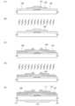
図1(A)に示すように、絶縁表面を有する基板100上にゲート電極101を設ける。
下地膜となる絶縁膜を基板100とゲート電極101の間に設けてもよい。下地膜は、基
板100からの不純物元素の拡散を防止する絶縁膜、具体的には、窒化珪素膜、酸化珪素
膜、窒化酸化珪素膜、又は酸化窒化珪素膜のうちの一を単層で用いるか、又は選択した複
数の膜を積層させて用いることができる。ゲート電極101の材料は、モリブデン、チタ
ン、クロム、タンタル、タングステン、アルミニウム、銅、ネオジム、スカンジウム等の
金属材料又はこれらを主成分とする合金材料を用いた導電膜を、単層で又は積層で用いる
ことができる。As shown in FIG. 1A, a
An insulating film serving as a base film may be provided between the
例えば、ゲート電極101の二層の積層構造としては、アルミニウム膜上にモリブデン膜
が積層された二層構造、または銅膜上にモリブデン膜を積層した二層構造、または銅膜上
に窒化チタン膜若しくは窒化タンタルを積層した二層構造、窒化チタン膜とモリブデン膜
とを積層した二層構造とすることが好ましい。三層の積層構造としては、タングステン膜
または窒化タングステン膜と、アルミニウムと珪素の合金膜またはアルミニウムとチタン
の合金膜と、窒化チタン膜またはチタン膜とを積層した三層構造とすることが好ましい。For example, the two-layered structure of the
なお、本明細書において酸化窒化物とは、その組成として、窒素よりも酸素の含有量が多
い物質であり、また、窒化酸化物とは、その組成として、酸素よりも窒素の含有量が多い
物質をいう。例えば、酸化窒化珪素とは、酸素が50原子%以上70原子%以下、窒素が
0.5原子%以上15原子%以下、珪素が25原子%以上35原子%以下、水素が0.1
原子%以上10原子%以下の範囲で含まれる物質とすることができる。また、窒化酸化珪
素とは、酸素が5原子%以上30原子%以下、窒素が20原子%以上55原子%以下、珪
素が25原子%以上35原子%以下、水素が10原子%以上30原子%以下の範囲で含ま
れる物質とすることができる。但し、上記組成の範囲は、ラザフォード後方散乱法(RB
S:Rutherford Backscattering Spectrometry
)や、水素前方散乱法(HFS:Hydrogen Forward Scatteri
ng)を用いて測定した場合のものである。また、構成元素の含有比率は、その合計が1
00原子%を超えない値をとる。In this specification, an oxynitride refers to a substance whose composition contains more oxygen than nitrogen, and a nitride oxide refers to a substance whose composition contains more nitrogen than oxygen. For example, silicon oxynitride refers to a substance whose composition contains 50 atomic % or more and 70 atomic % or less of oxygen, 0.5 atomic % or more and 15 atomic % or less of nitrogen, 25 atomic % or more and 35 atomic % or less of silicon, and 0.1 atomic % or less of hydrogen.
Silicon nitride oxide can be a substance containing oxygen in the range of 5 atomic % to 30 atomic %; nitrogen in the range of 20 atomic % to 55 atomic %; silicon in the range of 25 atomic % to 35 atomic %; and hydrogen in the range of 10 atomic % to 30 atomic %. However, the above composition ranges are determined by Rutherford backscattering spectrometry (RB
S: Rutherford Backscattering Spectrometry
) and Hydrogen Forward Scattering (HFS)
The content ratio of the constituent elements is measured when the total is 1
The value does not exceed 0.00 atomic %.
次いで、ゲート電極101上にゲート絶縁膜103を形成する。ゲート絶縁膜103は、
プラズマCVD法又はスパッタリング法等を用いて、酸化珪素膜、窒化珪素膜、酸化窒化
珪素膜又は窒化酸化珪素膜を単層で又は積層させて形成することができる。例えば、成膜
ガスとして、シラン(例えばモノシラン)、酸素及び窒素を用いてプラズマCVD法によ
り酸化窒化珪素膜を形成すれば良い。Next, a
A silicon oxide film, a silicon nitride film, a silicon oxynitride film, or a silicon nitride oxide film can be formed in a single layer or in a stacked layer by using a plasma CVD method, a sputtering method, etc. For example, a silicon oxynitride film may be formed by a plasma CVD method using silane (e.g., monosilane), oxygen, and nitrogen as a deposition gas.
次いで、ゲート絶縁膜103上に、酸化物半導体膜を形成する。なお、酸化物半導体膜を
スパッタ法により成膜する前に、アルゴンガスを導入してプラズマを発生させる逆スパッ
タを行い、ゲート絶縁膜103の表面に付着しているゴミを除去することが好ましい。逆
スパッタとは、ターゲット側に電圧を印加せずに、アルゴン雰囲気下で基板側にRF電源
を用いて電圧を印加して基板近傍にプラズマを形成して表面を改質する方法である。なお
、アルゴン雰囲気に代えて窒素、ヘリウムなどを用いてもよい。また、アルゴン雰囲気に
酸素、亜酸化窒素などを加えた雰囲気で行ってもよい。また、アルゴン雰囲気に塩素、四
フッ化炭素などを加えた雰囲気で行ってもよい。Next, an oxide semiconductor film is formed over the
チャネル形成領域を形成するための酸化物半導体膜には、半導体特性を有する酸化物材料
を用いればよく、例えば、In-Ga-Zn-O系非単結晶膜を用いる。酸化物半導体膜
は、In-Ga-Zn-O系酸化物半導体をターゲットとして用い、スパッタ法により成
膜する。また、酸化物半導体膜は、希ガス(例えばアルゴン)雰囲気下、酸素雰囲気下、
又は希ガス(例えばアルゴン)及び酸素雰囲気下においてスパッタ法により形成すること
ができる。The oxide semiconductor film for forming the channel formation region may be formed using an oxide material having semiconductor characteristics, for example, an In—Ga—Zn—O-based non-single crystal film. The oxide semiconductor film is formed by a sputtering method using an In—Ga—Zn—O-based oxide semiconductor as a target. The oxide semiconductor film is formed under a rare gas (e.g., argon) atmosphere, an oxygen atmosphere, or
Alternatively, it can be formed by a sputtering method in an atmosphere of rare gas (eg, argon) and oxygen.
ゲート絶縁膜103、及び酸化物半導体膜を大気に触れさせることなく連続的に形成して
もよい。大気に触れさせることなく連続成膜することで、界面が、水やハイドロカーボン
などの、大気成分や大気中に浮遊する不純物元素に汚染されることなく各積層界面を形成
することができるので、トランジスタ特性のばらつきを低減することができる。The
次いで、酸化物半導体膜をエッチングなどにより所望の形状に加工(パターニング)し、
島状の酸化物半導体膜104(第1の酸化物半導体膜)を形成する。なお、スパッタ等で
成膜された酸化物半導体膜中には、不純物である水分または水素が多量に含まれているこ
とが判明している。水分または水素はドナー準位を形成しやすいため、酸化物半導体にと
っては不純物である。そこで、図1(B)に示すように、不活性ガス雰囲気(窒素、また
はヘリウム、ネオン、アルゴン等)下、酸素雰囲気下、超乾燥空気雰囲気下、或いは減圧
下において、島状の酸化物半導体膜104にマイクロ波、高周波などの電磁波の照射を行
うことで、酸化物半導体膜中の水分または水素などの不純物を低減して、高純度化された
島状の酸化物半導体膜105(第2の酸化物半導体膜)を形成する。上記ガスは、水の含
有量が20ppm以下、好ましくは1ppm以下、好ましくは10ppb以下であること
が望ましい。Next, the oxide semiconductor film is processed (patterned) into a desired shape by etching or the like,
An island-shaped oxide semiconductor film 104 (first oxide semiconductor film) is formed. Note that it has been found that a large amount of moisture or hydrogen, which is an impurity, is contained in an oxide semiconductor film formed by sputtering or the like. Moisture or hydrogen is an impurity for an oxide semiconductor because it easily forms a donor level. Therefore, as shown in FIG. 1B, impurities such as moisture or hydrogen in the oxide semiconductor film are reduced by irradiating the island-shaped
マイクロ波の照射を行う場合、300MHz以上3THz以下、好ましくは300MHz
以上300GHz以下の周波数帯を用いることができる。また、高周波の照射を行う場合
、1MHz以上300MHz以下、好ましくは4MHz以上80MHz以下の周波数帯を
用いることができる。特に、電子レンジなどの電磁波発生装置において一般的に汎用され
ている、915MHz、2.45GHzの周波数を有するマイクロ波は、分極した水の分
子と共振しやすい。よって、上記周波数のマイクロ波は、水の損失係数が大きく、島状の
酸化物半導体膜104中の水分をより効率よく脱離させるのに有用である。例えば、2.
45GHzのマイクロ波を用いる場合、出力600Wで5分程度の照射を行うことで、高
純度化された島状の酸化物半導体膜105を形成することができる。When irradiating with microwaves, the frequency is 300 MHz or more and 3 THz or less, preferably 300 MHz.
A frequency band of 1 MHz to 300 MHz, preferably 4 MHz to 80 MHz, can be used for high-frequency irradiation. In particular, microwaves having frequencies of 915 MHz and 2.45 GHz, which are commonly used in electromagnetic wave generating devices such as microwave ovens, tend to resonate with polarized water molecules. Thus, microwaves of the above frequencies have a large water loss coefficient and are useful for more efficiently desorbing moisture from the island-shaped
In the case of using microwaves of 45 GHz, irradiation with microwaves at an output of 600 W for about five minutes can form a highly purified island-shaped
マイクロ波を用いる効果としては、マイクロ波の加熱効果を利用して、均一且つ急激に水
を加熱することで、通常の所謂加熱とは異なる化学反応を起こさせるというものである。
マイクロ波領域で起きている分子運動は、分子の回転や拡散のランダムな運動であり、結
果として加熱効果も生ずるが、非熱の効果も当然存在する。水を特徴づける誘電緩和は、
約25GHzのところに存在する。複素誘電率をε*=ε’-iε”とすると、虚部ε”
は、誘電損失と呼ばれる。虚部ε”の値が0でない周波数の電磁波を照射すると、その電
磁波は誘電体に吸収される。電子レンジの周波数は2.4GHzで、水の誘電損失のピー
クより約一桁小さいが、水の誘電損失のピークは、低い方は数GHz以下から高い方は遠
赤外領域まで拡がっているので、この領域の電磁波であれば水に吸収され、水の温度を上
げることができる。電子レンジは、水の誘電損失の低い方の裾野にエネルギーを与えて加
熱していることになる。水はDebye緩和で表現されることが知られている。Deby
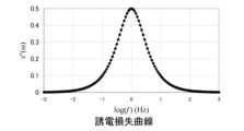
e緩和の場合、吸収曲線は図23の様に示される。図23の横軸は、電磁波の周波数fの
対数で表現されており、縦軸は誘電損失(虚部ε”)に角周波数ωを掛けた値を示してい
る。対応する電磁波の周波数における誘電損失は、図24で示される。誘電損失のピーク
値の周波数で、吸収曲線は最大値の約2分の1の値をとり、損失のスペクトルの高周波数
側の裾野で吸収係数が飽和する。効率よく加熱することを考えるならば、図23に示す吸
収曲線がある程度大きくなる周波数で、電力を投入するのが良いことが分かる。The effect of using microwaves is that the heating effect of microwaves is utilized to heat water uniformly and rapidly, thereby causing a chemical reaction different from that caused by ordinary so-called heating.
The molecular motion occurring in the microwave region is the random rotation and diffusion of molecules, which results in a heating effect, but of course there are also non-thermal effects. The dielectric relaxation that characterizes water is as follows:
It exists at about 25 GHz. If the complex dielectric constant is ε* = ε'-iε", the imaginary part ε"
is called the dielectric loss. When electromagnetic waves with a frequency where the imaginary part ε" is not zero are irradiated, the electromagnetic waves are absorbed by the dielectric. The frequency of a microwave oven is 2.4 GHz, which is about one order of magnitude lower than the peak of the dielectric loss of water. However, the peak of the dielectric loss of water extends from a few GHz on the low side to the far infrared region on the high side, so that electromagnetic waves in this region are absorbed by the water and the temperature of the water can be increased. In other words, a microwave oven heats water by providing energy to the low base of the dielectric loss of water. It is known that water can be expressed by Debye relaxation.
In the case of e-relaxation, the absorption curve is shown in FIG. 23. The horizontal axis in FIG. 23 is expressed as the logarithm of the frequency f of the electromagnetic wave, and the vertical axis indicates the value obtained by multiplying the dielectric loss (imaginary part ε") by the angular frequency ω. The dielectric loss at the corresponding electromagnetic wave frequency is shown in FIG. 24. At the frequency of the peak value of the dielectric loss, the absorption curve takes a value that is about half the maximum value, and the absorption coefficient saturates at the high-frequency foot of the loss spectrum. If efficient heating is considered, it will be understood that it is best to input power at a frequency where the absorption curve shown in FIG. 23 becomes somewhat large.
マイクロ波の照射は、マイクロ波を反射させることができる金属をその内壁に用いた処理
室内で行うことができる。この場合、マイクロ波は、マグネトロンなどを用いたマイクロ
波発生装置において生成された後、導波管により処理室内に導入され、被処理物に照射さ
れる。マイクロ波は高周波に比べて波長が短いため、光と同様に処理室内を自由に伝搬す
ることができる。被照射物に吸収されずに処理室内の内壁に照射されたマイクロ波は、内
壁において乱反射するので、最終的に被照射物に吸収されやすい。Microwave irradiation can be performed in a processing chamber whose inner wall is made of a metal capable of reflecting microwaves. In this case, microwaves are generated in a microwave generator using a magnetron or the like, and then introduced into the processing chamber through a waveguide, where they are irradiated onto the object to be processed. Since microwaves have a shorter wavelength than high frequencies, they can propagate freely within the processing chamber like light. Microwaves irradiated onto the inner wall of the processing chamber without being absorbed by the object to be irradiated are diffusely reflected by the inner wall, and are ultimately likely to be absorbed by the object to be irradiated.
高周波の照射は、処理室内において一対の電極間に被照射物を設置し、高周波発生回路を
用いて該電極間に高周波電圧を印加することで行うことができる。The radio frequency irradiation can be performed by placing the object to be irradiated between a pair of electrodes in a processing chamber and applying a radio frequency voltage between the electrodes using a radio frequency generating circuit.
なお、処理室内に導入する窒素、またはヘリウム、ネオン、アルゴン等の希ガスには、水
、水素などが含まれないことが好ましい。具体的に処理室に導入する窒素、またはヘリウ
ム、ネオン、アルゴン等の希ガスの純度は、6N(99.9999%)以上、好ましくは
7N(99.99999%)以上、(即ち不純物濃度を1ppm以下、好ましくは0.1
ppm以下)であることが好ましい。It is preferable that the nitrogen or rare gas such as helium, neon, or argon introduced into the processing chamber does not contain water, hydrogen, etc. Specifically, the purity of the nitrogen or rare gas such as helium, neon, or argon introduced into the processing chamber is 6N (99.9999%) or more, preferably 7N (99.99999%) or more (i.e., the impurity concentration is 1 ppm or less, preferably 0.1 ppm or less).
It is preferable that the content is less than 1 ppm.
或いは、窒素ガス雰囲気または希ガス雰囲気などの不活性ガス雰囲気に代えて、大気圧下
の露点がマイナス60℃以下の、水分含有量が少ない空気下において、電磁波の照射を行
うようにしても良い。Alternatively, instead of an inert gas atmosphere such as a nitrogen gas atmosphere or a rare gas atmosphere, electromagnetic waves may be irradiated in air with a low moisture content and a dew point of −60° C. or less at atmospheric pressure.
マイクロ波、高周波などの電磁波の照射による水分、水素、OHの脱離は、酸化物半導体
膜の内部に含まれる水分子内の結合子、水素と酸化物半導体の結合子、水酸基と酸化物半
導体の結合子などが、電磁波のエネルギーを吸収し、振動して切れることにより行われる
。よって、酸化物半導体膜の外部から内部へ熱伝導などによって徐々に熱を伝えていく外
部加熱を用いる場合よりも、効率よく上記結合子を切り離すことができるので、酸化物半
導体膜の温度の上昇を抑えつつ、水分、水素、OHを酸化物半導体膜から脱離させること
ができる。The desorption of moisture, hydrogen, and OH by irradiation with electromagnetic waves such as microwaves and high frequency waves occurs when bonds in water molecules contained inside the oxide semiconductor film, bonds between hydrogen and the oxide semiconductor, bonds between hydroxyl groups and the oxide semiconductor, etc., absorb the energy of the electromagnetic waves and vibrate and break. Therefore, the bonds can be cut more efficiently than when using external heating that gradually transfers heat from the outside to the inside of the oxide semiconductor film by thermal conduction, etc., and therefore moisture, hydrogen, and OH can be desorbed from the oxide semiconductor film while suppressing an increase in the temperature of the oxide semiconductor film.
水分、水素、OHなどの脱離により高純度化した酸化物半導体をチャネル形成領域に有す
るトランジスタは、閾値電圧の変動など、不純物によってもたらされる特性の劣化が抑え
られ、高い信頼性を得ることができる。A transistor having a channel formation region made of an oxide semiconductor that has been highly purified by eliminating moisture, hydrogen, OH, and the like can have high reliability because degradation of characteristics caused by impurities, such as a shift in threshold voltage, can be suppressed.
また、電磁波の照射と並行して、島状の酸化物半導体膜104に加熱処理を施しても良い
。電磁波の照射と加熱処理を併用する場合、不活性ガス雰囲気(窒素、またはヘリウム、
ネオン、アルゴン等)下、酸素雰囲気下、超乾燥空気雰囲気下、或いは減圧下において加
熱処理の設定温度まで島状の酸化物半導体膜104の温度を上昇させてから、上述した電
磁波の照射を行い、その後、上記雰囲気を維持した状態で、室温以上100℃未満の範囲
まで島状の酸化物半導体膜104を徐冷するのが望ましい。なお、減圧下で加熱処理を行
った場合は、加熱後に不活性ガスを流して大気圧に戻してから、冷却しても良い。上記ガ
スは、水の含有量が20ppm以下、好ましくは1ppm以下、好ましくは10ppb以
下であることが望ましい。In addition, heat treatment may be performed on the island-shaped
It is preferable to increase the temperature of the island-shaped
加熱処理は、酸化物半導体を構成しているZnなどの融点の低い金属が気化しにくい温度
、例えば100℃以上350℃未満、好ましくは150℃以上250℃未満で行う。電磁
波の照射を加熱処理と並行して行うことで、酸化物半導体膜中の水分などの不純物を、短
い時間でより効率よく低減することができる。The heat treatment is performed at a temperature at which a metal with a low melting point, such as Zn, which constitutes the oxide semiconductor, is not easily vaporized, for example, at a temperature of 100° C. or higher and lower than 350° C., preferably at a temperature of 150° C. or higher and lower than 250° C. By performing the electromagnetic wave irradiation in parallel with the heat treatment, impurities such as moisture in the oxide semiconductor film can be reduced more efficiently in a short time.
なお、室温で酸化物半導体膜に電磁波を照射したとしても、水分子が電磁波のエネルギー
を吸収して振動を行うため、結果的に酸化物半導体膜の温度は室温よりも高くなることが
予想される。加熱処理を電磁波の照射と並行して行う場合、電磁波の照射による温度上昇
分を考慮して、酸化物半導体膜の温度を管理することが望ましい。Note that even if the oxide semiconductor film is irradiated with electromagnetic waves at room temperature, the temperature of the oxide semiconductor film is expected to be higher than room temperature because water molecules absorb the energy of the electromagnetic waves and vibrate. When heat treatment is performed in parallel with the electromagnetic wave irradiation, it is preferable to manage the temperature of the oxide semiconductor film in consideration of the temperature increase due to the electromagnetic wave irradiation.
加熱処理は、電気炉を用いた加熱方法、加熱した気体を用いるGRTA(Gas Rap
id Thermal Anneal)法またはランプ光を用いるLRTA(Lamp
Rapid Thermal Anneal)法などの瞬間加熱方法などを用いることが
できる。例えば、電気炉を用いて加熱処理を行う場合、昇温特性を0.1℃/min以上
20℃/min以下、降温特性を0.1℃/min以上15℃/min以下とすることが
好ましい。Heat treatment can be performed using an electric furnace or a GRTA (Gas Rapid Transient Annealing) method using heated gas.
id Thermal Anneal (LRTA) method using lamp light or
For example, when the heat treatment is performed using an electric furnace, it is preferable that the temperature rise characteristic is 0.1° C./min to 20° C./min and the temperature fall characteristic is 0.1° C./min to 15° C./min.
加熱処理後の、島状の酸化物半導体膜105は、非晶質であることが好ましいが、一部結
晶化していても良い。After the heat treatment, the island-shaped
なお、酸化物半導体膜に電磁波の照射を行った後に、酸素雰囲気下で該酸化物半導体膜に
加熱処理を施すことで、酸化物半導体膜に含まれる水などの不純物を除去することができ
る。そして、酸素雰囲気下での加熱処理により、酸化物半導体膜を酸素が過剰な状態とす
ることで、高抵抗化できる。加熱処理の温度は、酸化物半導体を構成しているZnなどの
融点の低い金属が気化しにくい温度、例えば100℃以上350℃未満、好ましくは15
0℃以上250℃未満で行う。上記酸素雰囲気下の加熱処理に用いられる酸素ガスには、
水、水素などが含まれないことが好ましい。または、加熱処理装置に導入する酸素ガスの
純度を、6N(99.9999%)以上、好ましくは7N(99.99999%)以上、
(即ち酸素中の不純物濃度を1ppm以下、好ましくは0.1ppm以下)とすることが
好ましい。Note that impurities such as water contained in the oxide semiconductor film can be removed by performing heat treatment on the oxide semiconductor film in an oxygen atmosphere after the oxide semiconductor film is irradiated with electromagnetic waves. The heat treatment in the oxygen atmosphere can make the oxide semiconductor film have an excess of oxygen, thereby increasing the resistance of the oxide semiconductor film. The temperature of the heat treatment is set to a temperature at which a metal with a low melting point, such as Zn, which constitutes the oxide semiconductor, is not easily vaporized, for example, at 100° C. or higher and lower than 350° C., and preferably at 15° C. or higher.
The heat treatment is carried out at a temperature of 0° C. or higher and lower than 250° C. The oxygen gas used in the heat treatment in the oxygen atmosphere includes
It is preferable that the oxygen gas does not contain water, hydrogen, etc. Alternatively, the purity of the oxygen gas introduced into the heat treatment device is 6N (99.9999%) or more, preferably 7N (99.99999%) or more.
(That is, it is preferable to keep the impurity concentration in oxygen at 1 ppm or less, and preferably at 0.1 ppm or less).
次いで、ゲート絶縁膜103、島状の酸化物半導体膜105上に導電膜を形成する。上記
導電膜の材料としては、アルミニウム、クロム、タンタル、チタン、マンガン、マグネシ
ウム、モリブデン、タングステン、ジルコニウム、ベリリウム、トリウムから選ばれた元
素、または上記元素を1つまたは複数成分として含む合金等が挙げられる。Next, a conductive film is formed over the
なお、導電膜の形成後に加熱処理を行う場合には、この加熱処理に対する耐熱性を導電膜
に持たせることが好ましい。アルミニウム単体では耐熱性が劣り、また腐蝕しやすい等の
問題点があるので、導電膜の形成後に加熱処理を行う場合は、耐熱性導電性材料と組み合
わせて導電膜を形成する。アルミニウムと組み合わせる耐熱性導電性材料としては、チタ
ン、タンタル、タングステン、モリブデン、クロム、ネオジム、スカンジウムから選ばれ
た元素、または上記元素を1つまたは複数成分として含む合金、または上記元素を成分と
して含む窒化物などが好ましい。In addition, when a heat treatment is performed after the formation of a conductive film, it is preferable that the conductive film has heat resistance against the heat treatment. Since aluminum alone has problems such as poor heat resistance and susceptibility to corrosion, when a heat treatment is performed after the formation of a conductive film, the conductive film is formed in combination with a heat-resistant conductive material. As the heat-resistant conductive material to be combined with aluminum, an element selected from titanium, tantalum, tungsten, molybdenum, chromium, neodymium, and scandium, an alloy containing one or more of the above elements as a component, or a nitride containing the above elements as a component, is preferable.
次いで図1(C)に示すように、上記導電膜をエッチングなどにより所望の形状に加工(
パターニング)し、ソース電極106又はドレイン電極107を形成する。なお、上記パ
ターニングの際に、ソース電極106とドレイン電極107の形成によって、島状の酸化
物半導体膜の露出した部分が一部エッチングされることで、溝部(凹部)を有する島状の
酸化物半導体膜108が形成される。Next, as shown in FIG. 1C, the conductive film is processed into a desired shape by etching or the like.
The
そして、図1(D)に示すように、島状の酸化物半導体膜108に、不活性ガス雰囲気(
窒素、またはヘリウム、ネオン、アルゴン等)下、酸素雰囲気下、超乾燥空気雰囲気下、
或いは減圧下において、マイクロ波、高周波などの電磁波の照射を行うことで、高純度化
された島状の酸化物半導体膜109を形成する。上記ガスは、水の含有量が20ppm以
下、好ましくは1ppm以下、好ましくは10ppb以下であることが望ましい。島状の
酸化物半導体膜108へのマイクロ波、高周波などの電磁波の照射、または併用して行わ
れる加熱処理については、島状の酸化物半導体膜104に対して行ったマイクロ波、高周
波などの電磁波の照射についての説明を参照して、実施することができる。Then, as shown in FIG. 1D , the island-shaped
Nitrogen, helium, neon, argon, etc.), oxygen atmosphere, ultra-dry air atmosphere,
Alternatively, the island-shaped
本発明の一態様では、電磁波の照射により高温の加熱処理を施さなくとも、より低温で、
より短時間で、酸化物半導体中の水、水素、OHなどの不純物を脱離させることができる
。よって、水、水素、OHなどの不純物を脱離させるための加熱処理により、ソース電極
106及びドレイン電極107に含まれる金属が、島状の酸化物半導体膜108中に入り
込んでしまうのを防ぎ、オフ電流が高くなるなどのトランジスタの特性の劣化が生じてし
まうのを防ぐことができる。In one embodiment of the present invention, the heat treatment can be performed at a lower temperature without high-temperature heat treatment by irradiation with electromagnetic waves.
Impurities such as water, hydrogen, and OH in the oxide semiconductor can be eliminated in a shorter time. Therefore, the heat treatment for eliminating impurities such as water, hydrogen, and OH can prevent metal contained in the
また、本実施の形態では、パターニングにより形成された島状の酸化物半導体膜104に
対して電磁波の照射を行い、また、ソース電極106及びドレイン電極107を形成する
ことによって同時に形成された島状の酸化物半導体膜108に対しても再び電磁波の照射
を行っている。しかし、電磁波の照射は必ずしも2回行う必要はない。パターニングによ
り形成された島状の酸化物半導体膜104に対して行う電磁波の照射だけを実施しても良
いし、ソース電極106及びドレイン電極107を形成することによって同時に形成され
た島状の酸化物半導体膜108に対して行う電磁波の照射だけを実施しても良い。或いは
、上記2回の電磁波の照射のうち、パターニングにより形成された島状の酸化物半導体膜
104に対して電磁波の照射を行う代わりに、パターニングにより島状の酸化物半導体膜
104を形成する前の酸化物半導体膜に対して電磁波の照射を行う様にしても良い。或い
は、上記2回の電磁波の照射に加え、パターニングにより島状の酸化物半導体膜104を
形成する前の酸化物半導体膜に対して電磁波の照射を行う様にしても良い。或いは、パタ
ーニングにより島状の酸化物半導体膜104を形成する前の酸化物半導体膜に対して行う
電磁波の照射だけを実施するようにしても良い。In this embodiment, the island-shaped
次いで、図1(E)に示すように、島状の酸化物半導体膜109に接するように、スパッ
タ法で酸化物絶縁膜110を形成する。高純度化された島状の酸化物半導体膜109に接
して形成する酸化物絶縁膜110は、水分や、水素、OHなどの不純物を極力含まず、こ
れらが外部から侵入することをブロックする、酸化珪素膜、窒化酸化珪素膜などの無機絶
縁膜を用いる。1E, an
本実施の形態では、酸化物絶縁膜110として膜厚300nmの酸化珪素膜を成膜する。
成膜時の基板温度は、室温以上300℃以下とすればよく、本実施の形態では100℃と
する。酸化珪素膜のスパッタ法による成膜は、希ガス(例えばアルゴン)雰囲気下、酸素
雰囲気下、又は希ガス(例えばアルゴン)及び酸素雰囲気下において行うことができる。
また、ターゲットとして酸化珪素ターゲットを用いても珪素ターゲットを用いてもよい。
例えば珪素ターゲットを用いて、酸素、及び窒素雰囲気下でスパッタ法により酸化珪素膜
を形成することができる。In this embodiment, a silicon oxide film is formed as the
The substrate temperature during film formation may be from room temperature to 300° C. inclusive, and in this embodiment, is 100° C. The silicon oxide film can be formed by sputtering in a rare gas (e.g., argon) atmosphere, an oxygen atmosphere, or a rare gas (e.g., argon) and oxygen atmosphere.
As the target, a silicon oxide target or a silicon target may be used.
For example, a silicon oxide film can be formed by sputtering using a silicon target in an oxygen and nitrogen atmosphere.
高純度化された酸化物半導体膜105に接してスパッタ法またはPCVD法などにより酸
化物絶縁膜110を形成すると、電磁波の照射、或いは電磁波の照射と並行して行った加
熱処理により、酸化物半導体膜105に酸素欠損が発生していたとしても、酸化物半導体
膜105に酸素が供与される。そのため、酸化物半導体膜105の酸化物絶縁膜110と
接する領域において、ドナーとなる酸素欠損を低減し、化学量論比を満たすことができる
。その結果、酸化物半導体膜105をi型化または実質的にi型化することで形成される
酸化物半導体膜111(第3の酸化物半導体膜)を得ることができ、トランジスタの電気
特性の向上および、電気特性のばらつきを軽減することができる。When the
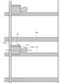
図2に、本実施の形態で作製したトランジスタ112の上面図を示す。図1(E)は、図
2の破線A1-A2における断面図に相当する。トランジスタ112は、ゲート電極10
1と、ゲート電極101上のゲート絶縁膜103と、ゲート絶縁膜103上の酸化物半導
体膜111と、酸化物半導体膜111上のソース電極106及びドレイン電極107とを
有する。2 shows a top view of a
1 , a
また、酸化物絶縁膜110を形成後、窒素雰囲気下、又は大気雰囲気下(大気中)におい
てトランジスタ112に加熱処理(好ましくは150℃以上350℃未満)を行ってもよ
い。例えば、窒素雰囲気下で250℃、1時間の加熱処理を行う。該加熱処理を行うと、
酸化物半導体膜105が酸化物絶縁膜110と接した状態で加熱されることになり、トラ
ンジスタ112の電気的特性のばらつきを軽減することができる。この加熱処理(好まし
くは150℃以上350℃未満)は、酸化物絶縁膜110の形成後であれば特に限定され
ず、他の工程、例えば樹脂膜形成時の加熱処理や、透明導電膜を低抵抗化させるための加
熱処理と兼ねることで、工程数を増やすことなく行うことができる。After the
The
なお、ソース電極106及びドレイン電極107を形成した後、島状の酸化物半導体膜1
08に電磁波を照射して島状の酸化物半導体膜109を形成する工程と、酸化物半導体膜
109に接するように酸化物絶縁膜110を形成する工程とを、大気に触れさせることな
く連続的に処理(連続処理、インサイチュ(insitu)工程)することで、最終的に
形成される酸化物半導体膜111中に含まれる水分や、水素、OHなどの不純物を、より
低減させることができる。その結果、トランジスタ112の信頼性を、より高めることが
できる。After the
By performing the step of forming the island-shaped
なお、作製工程において、島状の酸化物半導体膜108に電磁波を照射して島状の酸化物
半導体膜109を形成する工程と、酸化物絶縁膜110を形成する工程の間に、基板搬送
工程、アライメント工程、加熱または冷却する工程等を有しても、本明細書における連続
処理の範囲にあるとする。ただし、洗浄工程、ウェットエッチング、レジスト形成といっ
た液体を用いる工程が上記2つの工程間にある場合、本連続処理の範囲には当てはまらな
いとする。Note that in the manufacturing process, even if a substrate transport step, an alignment step, a heating step, a cooling step, or the like is included between a step of forming the island-shaped
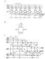
上述した連続処理は、例えばマイクロ波プラズマCVD装置を用いて行うことができる。
図22はマイクロ波プラズマCVD装置の反応室の構成を示す断面図である。マイクロ波
プラズマCVD装置の反応室には、処理容器180、処理容器180内に設けられ基板1
00を配置するための支持台181、処理容器180内にガスを導入するためのガス供給
部182、処理容器180内のガスを排気するために真空ポンプに接続する排気口183
、プラズマ発生用のマイクロ波を供給するマイクロ波発生装置184、マイクロ波発生装
置184からマイクロ波を処理容器180に導入する導波管185、導波管185に接し
且つ開口部187aを有する天板187、取り付け具188で天板187に設けられた複
数の誘電体板186が設けられる。The above-mentioned continuous processing can be carried out using, for example, a microwave plasma CVD device.
22 is a cross-sectional view showing the configuration of a reaction chamber of a microwave plasma CVD apparatus. The reaction chamber of the microwave plasma CVD apparatus includes a
1, a support table 181 for placing the wafer W, a
The
また、基板100及び誘電体板186の間に非原料ガスを流すガス管197、及び原料ガ
スを流すガス管198が設けられる。ガス管197、ガス管198は、ガス供給部182
と接続される。具体的には、非原料ガスを流すガス管197は、バルブ195及び質量流
量コントローラ193を介して非原料ガス供給源191に接続される。また、原料ガスを
流すガス管198は、バルブ196及び質量流量コントローラ194を介して非原料ガス
供給源192に接続される。また、支持台181に温度制御部199を設けることによっ
て、基板100の温度を制御することも可能である。また、支持台181に高周波電源を
接続し、高周波電源から出力された高周波電圧により、支持台181に所定のバイアス電
圧を印加する構成としてもよい。なお、ガス供給部182及びマイクロ波発生装置184
は反応室の外に設けられる。In addition, a
Specifically, a
is provided outside the reaction chamber.
マイクロ波発生装置184は、周波数が1GHz、2.45GHzまたは8.3GHzの
マイクロ波を供給することができる。なお、マイクロ波発生装置184を複数有すること
で、一辺が1000mmを超えるような大面積の基板に対して、一様にマイクロ波を照射
することができ、また、プラズマCVD法を用いて均一性の高い酸化物絶縁膜110を高
い成膜速度で形成することができる。The
処理容器180、及び天板187は、表面がアルミナ、酸化珪素、フッ素樹脂のいずれか
の絶縁膜で覆われた金属、例えばアルミニウムを含む合金で形成される。また、取り付け
具188は金属、例えばアルミニウムを含む合金で形成される。The
誘電体板186は、天板187の開口部に密着するように設けられる。マイクロ波発生装
置184で発生したマイクロ波が導波管185及び天板187の開口部を経て、誘電体板
186に伝播し、誘電体板186を透過して処理容器180内に放出される。The
誘電体板186は、サファイア、石英ガラス、アルミナ、酸化珪素、窒化珪素等のセラミ
ックスで形成される。なお、誘電体板186は、プラズマ700発生側に窪みが形成され
てもよい。当該窪みにより、安定したプラズマを生成することができる。一辺が1000
mmを超えるような大面積の基板に対して、一様にマイクロ波を照射することができ、ま
た、プラズマCVD法を用いて均一性の酸化物絶縁膜110を高い成膜速度で形成するこ
とができる。The
A large substrate having an area exceeding 1 mm can be uniformly irradiated with microwaves, and the
非原料ガスを流すガス管197と原料ガスを流すガス管198は、交差するように設けら
れており、非原料ガスを流すガス管197の吹出し口が誘電体板186側に設けられ、原
料ガスを流すガス管198の吹出し口が基板100側に設けられる。非原料ガスが誘電体
板186側に噴出させることにより、誘電体板186表面での成膜を回避しつつ、プラズ
マ170を発生させることができる。また、基板100により近い位置で原料ガスを噴出
すことが可能であり、成膜速度を高めることが可能である。ガス管197、ガス管198
は、アルミナ、窒化アルミニウム等のセラミックスで形成される。セラミックスはマイク
ロ波の透過率が高いため、ガス管197、ガス管198をセラミックスで形成することで
、誘電体板186の直下にガス管を設けても、電界の乱れが生じずプラズマの分布を均一
にすることができる。
are made of ceramics such as alumina, aluminum nitride, etc. Ceramics have high microwave transmittance, so by making
上記マイクロ波プラズマCVD装置を用いてマイクロ波の照射を行う場合は、処理容器1
80内を真空にした後、非原料ガス供給源191から窒素、ヘリウム、ネオンまたはアル
ゴンなどの不活性ガスを処理容器180内に導入する。加熱処理をマイクロ波の照射と並
行して行う場合は、マイクロ波の照射を行う前に基板100が所定の温度に達するように
、温度制御部199において支持台181の温度を制御する。なお、処理容器180内に
放出されたマイクロ波の電界エネルギーにより、非原料ガスがプラズマ化するが、当該プ
ラズマ170は、誘電体板186表面でより密度が高いため、基板100へのダメージを
低減することができる。When irradiating microwaves using the microwave plasma CVD apparatus, a
After evacuating the inside of the
そして、マイクロ波の照射を行った後、酸化物絶縁膜110を酸化珪素で成膜するには、
まず、基板100の温度を制御する。基板100は室温若しくは温度制御部199により
100℃~350℃に加熱する。そして、処理容器180内を真空にした後、プラズマ着
火用ガスとして、ヘリウム、アルゴン、ネオン、キセノン、クリプトン等の希ガスのいず
れか一種以上及び酸素ガスを導入する。希ガスと共に、酸素ガスを処理容器180内に導
入することで、プラズマの着火を容易とすることができる。After the microwave irradiation, the
First, the temperature of the
なお、マイクロ波の照射を行う段階で、既に処理容器180内にヘリウム、ネオンまたは
アルゴンを導入してある場合、あえて酸化物絶縁膜110を成膜する際に処理容器180
内の気体を入れ替えなくとも良い。また、マイクロ波の照射と加熱処理とを並行して行っ
た場合、加熱処理後に基板100の温度を下げずに、そのまま酸化物絶縁膜110を成膜
する工程に移行しても良い。Note that in the case where helium, neon, or argon has already been introduced into the
In addition, when microwave irradiation and heat treatment are performed in parallel, the process may proceed to the step of forming the
また、基板100と誘電体板186との間隔は、10mm~80mm(好ましくは10m
mから30mm)程度である。次に、処理容器180内を所定の圧力に保つ。処理容器1
80内の圧力は1~200Pa、好ましくは1~100Paとする。次に、マイクロ波発
生装置の電源をオンにし、マイクロ波発生装置184から導波管185にマイクロ波を供
給し、処理容器180内でプラズマを生成する。マイクロ波発生装置の出力は500~6
000W、好ましくは4000~6000Wとする。マイクロ波の導入によりプラズマの
励起を行うと、低電子温度(0.7eV以上3eV以下、好ましくは0.7eV以上1.
5eV以下)で高電子密度(1×10¹¹~1×1013cm-3以上)のプラズマを生
成することができる。次に、ガス管198から原料ガスを処理容器180内に導入する。
具体的には、酸素ガスの供給を停止し、原料ガスとして、シラン及び酸素を導入すること
で、基板100上に酸化珪素を有する酸化物絶縁膜110を形成することができる。次に
、原料ガスの供給を停止し、処理容器180内の圧力を低下し、マイクロ波発生装置18
4の電源をオフにする。The distance between the
Next, the inside of the
The pressure inside 80 is set to 1 to 200 Pa, preferably 1 to 100 Pa. Next, the power supply of the
000 W, preferably 4000 to 6000 W. When plasma is excited by introducing microwaves, a low electron temperature (0.7 eV to 3 eV, preferably 0.7 eV to 1.
5 eV or less) and high electron density (1×10¹¹ to 1×1013 cm−3 or more) plasma can be generated. Next, a source gas is introduced into the
Specifically, the supply of oxygen gas is stopped and silane and oxygen are introduced as source gases, so that the
Turn off the power to
なお、図22では、マイクロ波プラズマCVD装置の反応室の一つを例示しているが、マ
イクロ波プラズマCVD装置が複数の反応室を有し、該複数の反応室が直接連結している
か、或いは共通のチャンバーに連結していても良い。Although FIG. 22 shows an example of one reaction chamber of a microwave plasma CVD apparatus, the microwave plasma CVD apparatus may have multiple reaction chambers, and the multiple reaction chambers may be directly connected to each other or may be connected to a common chamber.
(実施の形態2)
本実施の形態では、実施の形態1で示したトランジスタ112とは構造が異なるトランジ
スタを有する、半導体装置の作製方法について説明する。なお、実施の形態1と同一部分
又は同様な機能を有する部分、及び工程は、実施の形態1と同様に行うことができるため
、繰り返しの説明は省略する。(Embodiment 2)
This embodiment describes a method for manufacturing a semiconductor device including a transistor having a structure different from that of the
半導体装置の作製方法について、図3及び図4を用いて説明する。The method for manufacturing a semiconductor device is explained using Figures 3 and 4.
図3(A)に示すように、絶縁表面を有する基板200上にゲート電極201を設ける。
下地膜となる絶縁膜を基板200とゲート電極201の間に設けてもよい。ゲート電極2
01の材料及びその構造については、実施の形態1に示したゲート電極101の材料及び
構造を参照すれば良い。下地膜は、基板200からの不純物元素の拡散を防止する絶縁膜
、具体的には、窒化珪素膜、酸化珪素膜、窒化酸化珪素膜、又は酸化窒化珪素膜のうちの
一を単層で用いるか、又は選択した複数の膜を積層させて用いることができる。As shown in FIG. 3A, a
An insulating film serving as a base film may be provided between the
For the material and structure of the
次いで、ゲート電極201上にゲート絶縁膜203を形成する。ゲート絶縁膜203は、
プラズマCVD法又はスパッタリング法等を用いて、酸化珪素膜、窒化珪素膜、酸化窒化
珪素膜又は窒化酸化珪素膜を単層で又は積層させて形成することができる。例えば、成膜
ガスとして、シラン(例えばモノシラン)、酸素及び窒素を用いてプラズマCVD法によ
り酸化窒化珪素膜を形成すれば良い。Next, a
A silicon oxide film, a silicon nitride film, a silicon oxynitride film, or a silicon nitride oxide film can be formed in a single layer or in a stacked layer by using a plasma CVD method, a sputtering method, etc. For example, a silicon oxynitride film may be formed by a plasma CVD method using silane (e.g., monosilane), oxygen, and nitrogen as a deposition gas.
次いで、ゲート絶縁膜203上に導電膜を形成する。そして、上記導電膜をエッチングな
どにより所望の形状に加工(パターニング)し、ソース電極206及びドレイン電極20
7を形成する。上記導電膜の材料については、実施の形態1においてソース電極106及
びドレイン電極107を形成する際にパターニングした導電膜の材料を参照すれば良い。Next, a conductive film is formed on the
Regarding the material of the conductive film, the material of the conductive film patterned when the
次いで、ソース電極206及びドレイン電極207及びゲート絶縁膜203上に、酸化物
半導体膜を形成する。そして、図3(B)に示すように、上記酸化物半導体膜をエッチン
グなどにより所望の形状に加工(パターニング)し、島状の酸化物半導体膜204(第1
の酸化物半導体膜)を形成する。Next, an oxide semiconductor film is formed over the
In the above process, an oxide semiconductor film (
チャネル形成領域を形成するための酸化物半導体膜には、実施の形態1において示した半
導体特性を有する酸化物材料を用いれば良い。酸化物半導体膜は、希ガス(例えばアルゴ
ン)雰囲気下、酸素雰囲気下、又は希ガス(例えばアルゴン)及び酸素雰囲気下において
スパッタ法により形成することができる。なお、酸化物半導体膜をスパッタ法により成膜
する前に、アルゴンガスを導入してプラズマを発生させる逆スパッタを行い、ゲート絶縁
膜203の表面に付着しているゴミを除去することが好ましい。The oxide semiconductor film for forming the channel formation region may be formed using the oxide material having the semiconductor characteristics described in
次いで、図3(C)に示すように、不活性ガス雰囲気(窒素、またはヘリウム、ネオン、
アルゴン等)下、酸素雰囲気下、超乾燥空気雰囲気下、或いは減圧下において、島状の酸
化物半導体膜204にマイクロ波、高周波などの電磁波の照射を行うことで、水分、水素
、OHなどの脱離により、高純度化された島状の酸化物半導体膜205(第2の酸化物半
導体膜)を形成する。上記ガスは、水の含有量が20ppm以下、好ましくは1ppm以
下、好ましくは10ppb以下であることが望ましい。上記電磁波の照射と並行して、島
状の酸化物半導体膜204に加熱処理を施しても良い。Next, as shown in FIG. 3C, an inert gas atmosphere (nitrogen, helium, neon,
The island-shaped
酸化物半導体膜204への電磁波の照射及び加熱処理については、実施の形態1において
示した、酸化物半導体膜104への電磁波の照射及び加熱処理についての説明を参照すれ
ば良い。For the irradiation of the
水分、水素、OHなどの脱離により高純度化した酸化物半導体をチャネル形成領域に有す
るトランジスタは、閾値電圧の変動など、不純物によってもたらされる特性の劣化が抑え
られ、高い信頼性を得ることができる。A transistor having a channel formation region made of an oxide semiconductor that has been highly purified by eliminating moisture, hydrogen, OH, and the like can have high reliability because degradation of characteristics caused by impurities, such as a shift in threshold voltage, can be suppressed.
また、本発明の一態様では、電磁波の照射により高温の加熱処理を施さなくとも、より低
温で、より短時間で、酸化物半導体中の水、水素、OHなどの不純物を脱離させることが
できる。よって、水、水素、OHなどの不純物を脱離させるための加熱処理により、ソー
ス電極206及びドレイン電極207に含まれる金属が、島状の酸化物半導体膜205中
に入り込んでしまうのを防ぎ、オフ電流が高くなるなどのトランジスタの特性の劣化が生
じてしまうのを防ぐことができる。In one embodiment of the present invention, impurities such as water, hydrogen, and OH in the oxide semiconductor can be eliminated at a lower temperature and in a shorter time without high-temperature heat treatment by electromagnetic wave irradiation. Therefore, the heat treatment for eliminating impurities such as water, hydrogen, and OH can prevent metal contained in the
また、本実施の形態では、パターニングにより形成された島状の酸化物半導体膜204に
対して電磁波の照射を行っているが、パターニング後ではなく、パターニング前の酸化物
半導体膜に対して電磁波の照射を行う様にしても良い。或いは、パターニング前とパター
ニング後の両方において、電磁波の照射を行う様にしても良い。Although the island-shaped
次いで、図3(D)に示すように、島状の酸化物半導体膜205に接するように、スパッ
タ法で酸化物絶縁膜210を形成する。高純度化された島状の酸化物半導体膜205に接
して形成する酸化物絶縁膜210は、水分や、水素、OHなどの不純物を極力含まず、こ
れらが外部から侵入することをブロックする、酸化珪素膜、窒化酸化珪素膜などの無機絶
縁膜を用いる。3D , an
本実施の形態では、酸化物絶縁膜210として膜厚300nmの酸化珪素膜を成膜する。
成膜時の基板温度は、室温以上300℃以下とすればよく、本実施の形態では100℃と
する。高純度化された酸化物半導体膜205に接してスパッタ法またはPCVD法などに
より酸化物絶縁膜210を形成すると、電磁波の照射、或いは電磁波の照射と並行して行
った加熱処理により、酸化物半導体膜205に酸素欠損が発生していたとしても、酸化物
半導体膜205に酸素が供与される。そのため、酸化物半導体膜205の酸化物絶縁膜2
10と接する領域において、ドナーとなる酸素欠損を低減し、化学量論比を満たすことが
できる。その結果、酸化物半導体膜205をi型化または実質的にi型化することで形成
される酸化物半導体膜211(第3の酸化物半導体膜)を得ることができ、トランジスタ
の電気特性の向上および、電気特性のばらつきを軽減することができる。In this embodiment, a silicon oxide film with a thickness of 300 nm is formed as the
The substrate temperature during film formation may be from room temperature to 300° C. inclusive, and is set to 100° C. in this embodiment. When the
In the region in contact with the
図4に、本実施の形態で作製したトランジスタ212の上面図を示す。図3(D)は、図
4の破線B1-B2における断面図に相当する。トランジスタ212は、ゲート電極20
1と、ゲート電極201上のゲート絶縁膜203と、ゲート絶縁膜203上のソース電極
206及びドレイン電極207と、ゲート絶縁膜203、ソース電極206及びドレイン
電極207上の酸化物半導体膜211とを有する。4 shows a top view of a
1 , a
また、酸化物絶縁膜210を形成後、窒素雰囲気下、又は大気雰囲気下(大気中)におい
てトランジスタ212に加熱処理(好ましくは150℃以上350℃未満)を行ってもよ
い。例えば、窒素雰囲気下で250℃、1時間の加熱処理を行う。該加熱処理を行うと、
酸化物半導体膜205が酸化物絶縁膜210と接した状態で加熱されることになり、トラ
ンジスタ212の電気的特性のばらつきを軽減することができる。この加熱処理(好まし
くは150℃以上350℃未満)は、酸化物絶縁膜210の形成後であれば特に限定され
ず、他の工程、例えば樹脂膜形成時の加熱処理や、透明導電膜を低抵抗化させるための加
熱処理と兼ねることで、工程数を増やすことなく行うことができる。After the
The
なお、ソース電極206及びドレイン電極207を形成した後、島状の酸化物半導体膜2
04に電磁波を照射して島状の酸化物半導体膜205を形成する工程と、酸化物半導体膜
205に接するように酸化物絶縁膜210を形成する工程とを、大気に触れさせることな
く連続的に処理(連続処理、インサイチュ(insitu)工程)することで、最終的に
形成される酸化物半導体膜205中に含まれる水分や、水素、OHなどの不純物を、より
低減させることができる。その結果、トランジスタ212の信頼性を、より高めることが
できる。After the
By performing the step of forming the island-shaped
また、本実施の形態は他の実施の形態と自由に組み合わせることができる。In addition, this embodiment can be freely combined with other embodiments.
(実施の形態3)
トランジスタを含む半導体装置の作製工程について、図5乃至図10を用いて説明する。(Embodiment 3)
A manufacturing process of a semiconductor device including a transistor will be described with reference to FIGS.
図5(A)において、透光性を有する基板400にはコーニング社の7059ガラスや1
737ガラスなどに代表されるバリウムホウケイ酸ガラスやアルミノホウケイ酸ガラスな
どのガラス基板を用いることができる。In FIG. 5A, a
A glass substrate such as barium borosilicate glass or aluminoborosilicate glass, typified by 737 glass, can be used.
次いで、導電膜を基板400全面に形成した後、第1のフォトリソグラフィ工程を行い、
レジストマスクを形成し、エッチングにより不要な部分を除去して配線及び電極(ゲート
電極401を含むゲート配線、容量配線408、及び第1の端子421)を形成する。こ
のとき少なくともゲート電極401の端部にテーパー形状が形成されるようにエッチング
する。Next, a conductive film is formed on the entire surface of the
A resist mask is formed, and unnecessary portions are removed by etching to form wirings and electrodes (a gate wiring including a
ゲート電極401を含むゲート配線と容量配線408、端子部の第1の端子421は、耐
熱性導電性材料としては、チタン、タンタル、タングステン、モリブデン、クロム、ネオ
ジム、スカンジウムから選ばれた元素、または上述した元素を成分とする合金か、上述し
た元素を組み合わせた合金膜、または上述した元素を成分とする窒化物で形成する。The gate wiring including the
次いで、図5(B)に示すように、ゲート電極401、容量配線408、第1の端子42
1上にゲート絶縁膜402を全面に成膜する。ゲート絶縁膜402はスパッタ法、PCV
D法などを用い、膜厚を50~250nmとする。Next, as shown in FIG. 5B, the
The
The film thickness is set to 50 to 250 nm using method D or the like.
例えば、ゲート絶縁膜402としてスパッタ法により酸化珪素膜を用い、100nmの厚
さで形成する。勿論、ゲート絶縁膜402はこのような酸化珪素膜に限定されるものでな
く、酸化窒化珪素膜、窒化珪素膜、酸化アルミニウム、酸化タンタル膜などの他の絶縁膜
を用い、これらの材料から成る単層または積層構造として形成しても良い。For example, a silicon oxide film is formed by sputtering to a thickness of 100 nm as the
次に、ゲート絶縁膜402上に、酸化物半導体膜403(In-Ga-Zn-O系非単結
晶膜)を成膜する。プラズマ処理後、大気に曝すことなくIn-Ga-Zn-O系非単結
晶膜を成膜することは、ゲート絶縁膜402と酸化物半導体膜403の界面にゴミや水分
を付着させない点で有用である。ここでは、直径8インチのIn、Ga、及びZnを含む
酸化物半導体ターゲット(In-Ga-Zn-O系酸化物半導体ターゲット(In2O3
:Ga2O3:ZnO=1:1:1))を用いて、基板400とターゲットの間の距離を
170mm、圧力0.4Pa、直流(DC)電源0.5kW、酸素のみ、アルゴンのみ、
又はアルゴン及び酸素雰囲気下で成膜する。なお、パルス直流(DC)電源を用いると、
ごみが軽減でき、膜厚分布も均一となるために好ましい。In-Ga-Zn-O系非単結
晶膜の膜厚は、5nm~200nmとする。本実施の形態では、例えば酸化物半導体膜4
03として、In-Ga-Zn-O系酸化物半導体ターゲットを用いてスパッタ法により
膜厚50nmのIn-Ga-Zn-O系非単結晶膜を成膜する。Next, an oxide semiconductor film 403 (In—Ga—Zn—O-based non-single crystal film) is formed over the
:Ga2 O3 :ZnO=1:1:1), the distance between the
Alternatively, the film is formed under an atmosphere of argon and oxygen. When a pulsed direct current (DC) power source is used,
This is preferable because it is possible to reduce dust and to make the film thickness distribution uniform. The film thickness of the In—Ga—Zn—O-based non-single crystal film is set to 5 nm to 200 nm. In this embodiment, for example, the
As step 03, an In-Ga-Zn-O-based non-single crystal film is formed to a thickness of 50 nm by a sputtering method using an In-Ga-Zn-O-based oxide semiconductor target.
スパッタ法にはスパッタ用電源に高周波電源を用いるRFスパッタ法と、DCスパッタ法
があり、さらにパルス的にバイアスを与えるパルスDCスパッタ法もある。RFスパッタ
法は主に絶縁膜を成膜する場合に用いられ、DCスパッタ法は主に金属膜を成膜する場合
に用いられる。There are two types of sputtering: RF sputtering, which uses a high-frequency power source as the sputtering power source, and DC sputtering, which also has a pulsed DC sputtering method that applies a bias in a pulsed manner. RF sputtering is mainly used when depositing insulating films, and DC sputtering is mainly used when depositing metal films.
また、材料の異なるターゲットを複数設置できる多元スパッタ装置もある。多元スパッタ
装置は、同一チャンバーで異なる材料膜を積層成膜することも、同一チャンバーで複数種
類の材料を同時に放電させて成膜することもできる。There are also multi-target sputtering devices that can accommodate multiple targets of different materials. Multi-target sputtering devices can deposit layers of different materials in the same chamber, or deposit films by discharging multiple types of materials simultaneously in the same chamber.
また、チャンバー内部に磁石機構を備えたマグネトロンスパッタ法を用いるスパッタ装置
や、グロー放電を使わずマイクロ波を用いて発生させたプラズマを用いるECRスパッタ
法を用いるスパッタ装置がある。There are also sputtering devices that use a magnetron sputtering method equipped with a magnet mechanism inside the chamber, and sputtering devices that use an ECR sputtering method that uses plasma generated by microwaves without using glow discharge.
また、スパッタ法を用いる成膜方法として、成膜中にターゲット物質とスパッタガス成分
とを化学反応させてそれらの化合物薄膜を形成するリアクティブスパッタ法や、成膜中に
基板にも電圧をかけるバイアススパッタ法もある。Other examples of film formation methods using sputtering include reactive sputtering, which forms a compound thin film by chemically reacting a target material with sputtering gas components during film formation, and bias sputtering, which also applies a voltage to the substrate during film formation.
次に、図5(C)に示すように、第2のフォトリソグラフィ工程を行い、レジストマスク
を形成し、酸化物半導体膜403をエッチングする。例えば燐酸と酢酸と硝酸を混ぜた溶
液を用いたウェットエッチングにより、不要な部分を除去して島状の酸化物半導体膜40
4をゲート電極401と重なるように形成する。なお、ここでのエッチングは、ウェット
エッチングに限定されずドライエッチングを用いてもよい。5C, a second photolithography process is performed to form a resist mask, and the
4 is formed so as to overlap with the
ドライエッチングに用いるエッチングガスとしては、塩素を含むガス(塩素系ガス、例え
ば塩素(Cl2)、塩化硼素(BCl3)、塩化珪素(SiCl4)、四塩化炭素(CC
l4)など)が好ましい。The etching gas used in the dry etching is a gas containing chlorine (a chlorine-based gas, for example, chlorine (Cl2 ), boron chloride (BCl3 ), silicon chloride (SiCl4 ), carbon tetrachloride (CC
l4 ) and the like) are preferred.
また、フッ素を含むガス(フッ素系ガス、例えば四弗化炭素(CF4)、弗化硫黄(SF
6)、弗化窒素(NF3)、トリフルオロメタン(CHF3)など)、臭化水素(HBr
)、酸素(O2)、これらのガスにヘリウム(He)やアルゴン(Ar)などの希ガスを
添加したガス、などを用いることができる。In addition, gases containing fluorine (fluorine-based gases, for example, carbon tetrafluoride (CF4 ), sulfur fluoride (SF
6 ), nitrogen fluoride (NF3 ), trifluoromethane (CHF3 ), etc.), hydrogen bromide (HBr
), oxygen (O2 ), or a gas obtained by adding a rare gas such as helium (He) or argon (Ar) to these gases, or the like, can be used.
ドライエッチング法としては、平行平板型RIE(Reactive Ion Etch
ing)法や、ICP(Inductively Coupled Plasma:誘導
結合型プラズマ)エッチング法を用いることができる。所望の加工形状にエッチングでき
るように、エッチング条件(コイル型の電極に印加される電力量、基板側の電極に印加さ
れる電力量、基板側の電極温度等)を適宜調節する。As the dry etching method, a parallel plate type RIE (Reactive Ion Etch) is used.
In order to etch into a desired shape, the etching conditions (such as the amount of power applied to the coil-shaped electrode, the amount of power applied to the electrode on the substrate side, and the temperature of the electrode on the substrate side) are appropriately adjusted.
ウェットエッチングに用いるエッチング液としては、燐酸と酢酸と硝酸を混ぜた溶液など
を用いることができる。また、ITO07N(関東化学社製)を用いてもよい。The etching solution used for the wet etching may be a mixture of phosphoric acid, acetic acid, and nitric acid, or ITO07N (manufactured by Kanto Chemical Co., Ltd.).
また、ウェットエッチング後のエッチング液はエッチングされた材料とともに洗浄によっ
て除去される。その除去された材料を含むエッチング液の廃液を精製し、含まれる材料を
再利用してもよい。当該エッチング後の廃液から酸化物半導体膜に含まれるインジウム等
の材料を回収して再利用することにより、資源を有効活用し低コスト化することができる
。In addition, the etching solution after the wet etching is removed by washing together with the etched materials. The waste liquid of the etching solution containing the removed materials may be refined and the contained materials may be reused. By recovering and reusing materials such as indium contained in the oxide semiconductor film from the waste liquid after the etching, resources can be effectively utilized and costs can be reduced.
所望の形状に加工できるように、材料に合わせてエッチング条件(エッチング液、エッチ
ング時間、温度等)を適宜調節する。The etching conditions (etching solution, etching time, temperature, etc.) are adjusted appropriately according to the material so that the desired shape can be obtained.
次に、図6(A)に示すように、不活性ガス雰囲気(窒素、またはヘリウム、ネオン、ア
ルゴン等)下、酸素雰囲気下、超乾燥空気雰囲気下、或いは減圧下において、酸化物半導
体膜404に電磁波の照射を行う。電磁波の照射と並行して加熱処理を行っても良い。上
記ガスは、水の含有量が20ppm以下、好ましくは1ppm以下、好ましくは10pp
b以下であることが望ましい。電磁波の照射により、水分、水素、OHなどの不純物が脱
離することで高純度化された酸化物半導体膜405が形成される。6A, the
By irradiation with electromagnetic waves, impurities such as moisture, hydrogen, and OH are eliminated, so that a highly purified
例えば、窒素雰囲気下において、2.45GHzのマイクロ波を用い、出力600Wで5
分程度の照射を行うことで、高純度化された島状の酸化物半導体膜405を形成すること
ができる。加熱処理を並行して行う場合、酸化物半導体を構成しているZnなどの融点の
低い金属が気化しにくい温度、例えば100℃以上350℃未満、好ましくは150℃以
上250℃未満で行う。電磁波の照射を加熱処理と並行して行うことで、酸化物半導体膜
中の水分などの不純物を、短い時間でより効率よく低減することができる。この場合、電
磁波の照射は、基板400の温度が加熱処理による設定温度に達した状態で行う。For example, in a nitrogen atmosphere, a microwave of 2.45 GHz is used, and the output is 600 W and the
By performing irradiation for about minutes, a highly purified island-shaped
なお、図6(A)の破線C1-C2の範囲内の断面図と、破線D1-D2の範囲内の断面
図は、図8に示す平面図の、破線C1-C2における断面図と、破線D1-D2における
断面図に相当する。Note that the cross-sectional view within the range of dashed line C1-C2 and the cross-sectional view within the range of dashed line D1-D2 in FIG. 6A correspond to the cross-sectional view along dashed line C1-C2 and the cross-sectional view along dashed line D1-D2 in the plan view shown in FIG. 8.
次に、図6(B)に示すように、酸化物半導体膜405上に金属材料からなる導電膜40
6をスパッタ法や真空蒸着法で形成する。導電膜406の材料としては、アルミニウム、
クロム、タンタル、チタン、モリブデン、タングステンから選ばれた元素、または上述し
た元素を成分とする合金か、上述した元素を組み合わせた合金膜等が挙げられる。Next, as shown in FIG. 6B , a
The
Examples of the film include an element selected from chromium, tantalum, titanium, molybdenum, and tungsten, an alloy containing the above elements, and an alloy film of a combination of the above elements.
導電膜406を形成した後に加熱処理を行う場合には、この加熱処理に耐える耐熱性を導
電膜に持たせることが好ましい。In the case where heat treatment is performed after the
次に、図6(C)に示すように、第3のフォトリソグラフィ工程を行い、レジストマスク
を形成し、エッチングにより不要な部分を除去してソース電極407a及びドレイン電極
407b、及び第2の端子420を形成する。この際のエッチング方法としてウェットエ
ッチングまたはドライエッチングを用いる。例えば導電膜406としてアルミニウム膜、
又はアルミニウム合金膜を用いる場合は、燐酸と酢酸と硝酸を混ぜた溶液を用いたウェッ
トエッチングを行うことができる。また、アンモニア過水を用いたウェットエッチングに
より、導電膜406をエッチングしてソース電極407a及びドレイン電極407bを形
成してもよい。6C, a third photolithography process is performed to form a resist mask, and unnecessary portions are removed by etching to form the
Alternatively, in the case of using an aluminum alloy film, wet etching using a mixed solution of phosphoric acid, acetic acid, and nitric acid can be performed. Alternatively, the
このエッチング工程において、酸化物半導体膜405の露出領域も一部エッチングされ、
島状の酸化物半導体膜409となる。よって、ソース電極407a又はドレイン電極40
7bの間の酸化物半導体膜409は膜厚の薄い領域となる。In this etching step, the exposed region of the
The
The
この第3のフォトリソグラフィ工程において、ソース電極407a及びドレイン電極40
7bと同じ材料である第2の端子420を端子部に残す。なお、第2の端子420はソー
ス配線(ソース電極407aを含むソース配線)と電気的に接続されている。In this third photolithography step, the
The
また、多階調マスクにより形成した複数(例えば二種類)の厚さの領域を有するレジスト
マスクを用いると、レジストマスクの数を減らすことができるため、工程簡略化、低コス
ト化が図れる。Furthermore, by using a resist mask having regions of a plurality of thicknesses (for example, two types) formed by a multi-tone mask, the number of resist masks can be reduced, which simplifies the process and reduces costs.
次に、レジストマスクを除去し、図7(A)に示すように、不活性ガス雰囲気(窒素、ま
たはヘリウム、ネオン、アルゴン等)下、酸素雰囲気下、超乾燥空気雰囲気下、或いは減
圧下において、酸化物半導体膜409に電磁波の照射を行う。上記ガスは、水の含有量が
20ppm以下、好ましくは1ppm以下、好ましくは10ppb以下であることが望ま
しい。電磁波の照射と並行して加熱処理を行っても良い。電磁波の照射により、水分、水
素、OHなどの不純物が脱離することで高純度化された酸化物半導体膜410が形成され
る。なお、酸化物半導体膜409への電磁波の照射、加熱処理については、島状の酸化物
半導体膜404に対して行った電磁波の照射の説明を参照して、実施することが可能であ
る。Next, the resist mask is removed, and the
本発明の一態様では、電磁波の照射により高温の加熱処理を施さなくとも、より低温で、
より短時間で、酸化物半導体中の水、水素、OHなどの不純物を脱離させることができる
。よって、水、水素、OHなどの不純物を脱離させるための加熱処理により、ソース電極
407a及びドレイン電極407bに含まれる金属が、島状の酸化物半導体膜410中に
入り込んでしまうのを防ぎ、オフ電流が高くなるなどのトランジスタの特性の劣化が生じ
てしまうのを防ぐことができる。In one embodiment of the present invention, the heat treatment can be performed at a lower temperature without high-temperature heat treatment by irradiation with electromagnetic waves.
Impurities such as water, hydrogen, and OH in the oxide semiconductor can be eliminated in a shorter time. Therefore, the heat treatment for eliminating impurities such as water, hydrogen, and OH can prevent metal contained in the
また、本実施の形態では、パターニングにより形成された島状の酸化物半導体膜404に
対して電磁波の照射を行い、また、ソース電極407a及びドレイン電極407bを形成
することによって同時に形成された島状の酸化物半導体膜409に対しても再び電磁波の
照射を行っている。しかし、電磁波の照射は必ずしも2回行う必要はない。パターニング
により形成された島状の酸化物半導体膜404に対して行う電磁波の照射だけを実施して
も良いし、ソース電極407a及びドレイン電極407bを形成することによって同時に
形成された島状の酸化物半導体膜409に対して行う電磁波の照射だけを実施しても良い
。或いは、上記2回の電磁波の照射のうち、パターニングにより形成された島状の酸化物
半導体膜404に対して電磁波の照射を行う代わりに、パターニングにより島状の酸化物
半導体膜404を形成する前の酸化物半導体膜403に対して電磁波の照射を行う様にし
ても良い。或いは、上記2回の電磁波の照射に加え、酸化物半導体膜403に対して電磁
波の照射を行う様にしても良い。或いは、酸化物半導体膜403に対して行う電磁波の照
射だけを実施するようにしても良い。In this embodiment, the island-shaped
なお、図7(A)の破線C1-C2の範囲内の断面図と、破線D1-D2の範囲内の断面
図は、図9に示す平面図の、破線C1-C2における断面図と、破線D1-D2における
断面図に相当する。Note that the cross-sectional view within the range of dashed line C1-C2 and the cross-sectional view within the range of dashed line D1-D2 in FIG. 7A correspond to the cross-sectional view along dashed line C1-C2 and the cross-sectional view along dashed line D1-D2 in the plan view shown in FIG.
次に、図7(B)に示すように、ゲート絶縁膜402、酸化物半導体膜410、ソース電
極407a及びドレイン電極407bを覆う酸化物絶縁膜411を形成する。酸化物絶縁
膜411はPCVD法により形成する酸化窒化珪素膜を用いる。ソース電極407a及び
ドレイン電極407bの間に設けられた酸化物半導体膜410の露出領域と酸化物絶縁膜
411である酸化窒化珪素膜が接して設けられることによって、電磁波の照射、或いは電
磁波の照射と並行して行った加熱処理により、酸化物半導体膜410に酸素欠損が発生し
ていたとしても、酸化物半導体膜410に酸素が供与される。そのため、酸化物半導体膜
410の酸化物絶縁膜411と接する領域において、ドナーとなる酸素欠損を低減し、化
学量論比を満たすことができる。その結果、酸化物半導体膜410をi型化または実質的
にi型化することで形成される酸化物半導体膜412を得ることができ、トランジスタの
電気特性の向上および、電気特性のばらつきを軽減することができる。Next, as shown in FIG. 7B , an
次いで、酸化物絶縁膜411を形成した後、加熱処理を行ってもよい。加熱処理は大気雰
囲気下、又は窒素雰囲気下において、150℃以上350℃未満で行えばよい。該加熱処
理を行うと、酸化物半導体膜412が酸化物絶縁膜411と接した状態で加熱されること
になり、さらに酸化物半導体膜412を高抵抗化させてトランジスタの電気特性の向上お
よび、電気特性のばらつきを軽減することができる。この加熱処理(好ましくは150℃
以上350℃未満)は、酸化物絶縁膜411の形成後であれば特に限定されず、他の工程
、例えば樹脂膜形成時の加熱処理や、透明導電膜を低抵抗化させるための加熱処理と兼ね
ることで、工程数を増やすことなく行うことができる。Next, after the
The heating step (heat treatment at a temperature of 300° C. or higher but lower than 350° C.) can be performed without increasing the number of steps by combining it with another step, such as a heat treatment for forming a resin film or a heat treatment for reducing the resistance of a transparent conductive film, as long as it is performed after the formation of the
以上の工程でトランジスタ413が作製できる。
次に、第4のフォトリソグラフィ工程を行い、レジストマスクを形成し、酸化物絶縁膜4
11及びゲート絶縁膜402のエッチングによりコンタクトホールを形成し、ドレイン電
極407bの一部、第1の端子421の一部、第2の端子420の一部を露出させる。次
いで、レジストマスクを除去した後、透明導電膜を成膜する。透明導電膜の材料としては
、酸化インジウム(In2O3)や酸化インジウム酸化スズ合金(In2O3―SnO2
、ITOと略記する)などをスパッタ法や真空蒸着法などを用いて形成する。このような
材料のエッチング処理は塩酸系の溶液により行う。しかし、特にITOのエッチングは残
渣が発生しやすいので、エッチング加工性を改善するために酸化インジウム酸化亜鉛合金
(In2O3―ZnO)を用いても良い。また、透明導電膜を低抵抗化させるための加熱
処理を行う場合、酸化物半導体膜412を高抵抗化させてトランジスタの電気特性の向上
および、電気特性のばらつきを軽減する熱処理と兼ねることができる。Next, a fourth photolithography process is performed to form a resist mask, and an
Contact holes are formed by etching the
A metal oxide such as ITO (indium oxide, abbreviated as ITO) is formed by sputtering or vacuum deposition. Such a material is etched using a hydrochloric acid-based solution. However, since the etching of ITO is particularly prone to leaving residues, an indium oxide-zinc oxide alloy (In2 O3 -ZnO) may be used to improve the etching processability. When heat treatment is performed to reduce the resistance of the transparent conductive film, the
次に、第5のフォトリソグラフィ工程を行い、レジストマスクを形成し、エッチングによ
り不要な部分を除去してドレイン電極407bに接続された画素電極414と、第1の端
子421に接続された透明導電膜415と、第2の端子420に接続された透明導電膜4
16とを形成する。Next, a fifth photolithography process is performed, a resist mask is formed, and unnecessary portions are removed by etching to obtain the
16 is formed.
透明導電膜415、416はFPCとの接続に用いられる電極または配線となる。第1の
端子421上に形成された透明導電膜415は、ゲート配線の入力端子として機能する接
続用の端子電極となる。第2の端子420上に形成された透明導電膜416は、ソース配
線の入力端子として機能する接続用の端子電極である。The transparent
この第5のフォトリソグラフィ工程において、ゲート絶縁膜402及び酸化物絶縁膜41
1を誘電体として、容量配線408と画素電極414とで保持容量が形成される。In the fifth photolithography step, the
A storage capacitor is formed by the
レジストマスクを除去した段階での断面図を図7(C)に示す。なお、図7(C)の破線
C1-C2の範囲内の断面図と、破線D1-D2の範囲内の断面図は、図10に示す平面
図の、破線C1-C2における断面図と、破線D1-D2における断面図に相当する。A cross-sectional view at the stage where the resist mask has been removed is shown in Fig. 7C. Note that the cross-sectional view within the range of the dashed lines C1-C2 and D1-D2 in Fig. 7C corresponds to the cross-sectional view along the dashed lines C1-C2 and D1-D2 in the plan view shown in Fig. 10.
こうして5回のフォトリソグラフィ工程により、5枚のフォトマスクを使用して、ボトム
ゲート型のスタガ構造のトランジスタであるトランジスタ413を有する画素トランジス
タ部、保持容量を完成させることができる。そして、これらを個々の画素に対応してマト
リクス状に配置して画素部を構成することによりアクティブマトリクス型の表示装置を作
製するための一方の基板とすることができる。本明細書では便宜上このような基板をアク
ティブマトリクス基板と呼ぶ。In this way, five photolithography steps are performed using five photomasks to complete a pixel transistor portion having the
アクティブマトリクス型の液晶表示装置を作製する場合には、アクティブマトリクス基板
と、対向電極が設けられた対向基板との間に液晶層を設け、アクティブマトリクス基板と
対向基板とを固定する。When an active matrix type liquid crystal display device is manufactured, a liquid crystal layer is provided between an active matrix substrate and a counter substrate having a counter electrode provided thereon, and the active matrix substrate and the counter substrate are fixed together.
また、容量配線を設けず、画素電極を隣り合う画素のゲート配線と酸化物絶縁膜及びゲー
ト絶縁膜を介して重ねて保持容量を形成してもよい。Alternatively, instead of providing a capacitance line, a pixel electrode may be overlapped with the gate line of an adjacent pixel via an oxide insulating film and a gate insulating film to form a storage capacitor.
アクティブマトリクス型の液晶表示装置においては、マトリクス状に配置された画素電極
を駆動することによって、画面上に表示パターンが形成される。具体的には、選択された
画素電極と該画素電極に対応する対向電極の間に電圧が印加されることによって、画素電
極と対向電極の間に生じた電界によって液晶層の光学変調が行われ、この光学変調が表示
パターンとして観察者に認識される。In an active matrix liquid crystal display device, a display pattern is formed on a screen by driving pixel electrodes arranged in a matrix. Specifically, a voltage is applied between a selected pixel electrode and a counter electrode corresponding to the pixel electrode, and an electric field is generated between the pixel electrode and the counter electrode, which causes optical modulation of the liquid crystal layer. This optical modulation is recognized by an observer as a display pattern.
液晶表示装置の動画表示において、液晶分子自体の応答が遅いため、残像が生じる、また
は動画のぼけが生じるという問題がある。液晶表示装置の動画特性を改善するため、全面
黒表示を1フレームおきに行う、所謂、黒挿入と呼ばれる駆動技術がある。In moving image display on a liquid crystal display device, the response of the liquid crystal molecules themselves is slow, which can cause problems such as afterimages or blurred moving images. In order to improve the moving image characteristics of a liquid crystal display device, there is a driving technique called black insertion, which displays a full black screen every other frame.
また、フレーム周期数を通常のフレーム周波数(60Hz)の1.5倍、好ましくは2倍
以上にすることで動画特性を改善する、所謂、倍速駆動と呼ばれる駆動技術もある。There is also a driving technique called double-speed driving, which improves moving image characteristics by increasing the frame frequency to 1.5 times, preferably 2 times or more, the normal frame frequency (60 Hz).
また、液晶表示装置の動画特性を改善するため、バックライトとして複数のLED(発光
ダイオード)光源または複数のEL光源などを用いて面光源を構成し、面光源を構成して
いる各光源を独立して1フレーム期間内で間欠点灯駆動する駆動技術もある。面光源とし
て、3種類以上のLEDを用いてもよいし、白色発光のLEDを用いてもよい。独立して
複数のLEDを制御できるため、液晶層の光学変調の切り替えタイミングに合わせてLE
Dの発光タイミングを同期させることもできる。この駆動技術は、LEDを部分的に消灯
することができるため、特に一画面を占める黒い表示領域の割合が多い映像表示の場合に
は、消費電力の低減効果が図れる。Also, in order to improve the moving image characteristics of a liquid crystal display device, there is a driving technology in which a surface light source is formed using a plurality of LED (light emitting diode) light sources or a plurality of EL light sources as a backlight, and each light source constituting the surface light source is independently driven to be intermittently lit within one frame period. As a surface light source, three or more types of LEDs may be used, or a white light emitting LED may be used. Since a plurality of LEDs can be controlled independently, the LEDs can be controlled in accordance with the switching timing of the optical modulation of the liquid crystal layer.
It is also possible to synchronize the light emission timing of the LEDs. This driving technology can partially turn off the LEDs, which can reduce power consumption, especially in the case of video displays that have a large proportion of black display areas occupying the entire screen.
これらの駆動技術を組み合わせることによって、液晶表示装置の動画特性などの表示特性
を従来よりも改善することができる。By combining these driving techniques, it is possible to improve the display characteristics, such as the moving image characteristics, of a liquid crystal display device compared to the conventional ones.
本明細書に開示するnチャネル型のトランジスタは、酸化物半導体膜をチャネル形成領域
に用いており、良好な動特性を有するため、これらの駆動技術を組み合わせることができ
る。The n-channel transistor disclosed in this specification uses an oxide semiconductor film for a channel formation region and has favorable dynamic characteristics; therefore, these driving techniques can be combined.
発光表示装置を作製する際、各有機発光素子の間に有機樹脂膜を用いた隔壁を設ける場合
がある。その場合には、有機樹脂膜を加熱処理するため、トランジスタの電気特性の向上
および、電気特性のばらつきを軽減する熱処理と兼ねることができる。When manufacturing a light-emitting display device, a partition using an organic resin film may be provided between each organic light-emitting element. In this case, the organic resin film is subjected to a heat treatment, which can serve as a heat treatment for improving the electrical characteristics of the transistor and reducing the variation in the electrical characteristics.
酸化物半導体を用いたトランジスタで形成することにより、製造コストを低減することが
できる。特に、電磁波の照射による水分、水素、OHなどの不純物の低減によって酸化物
半導体膜の純度を高めるため、成膜チャンバー内の露点を下げた特殊なスパッタ装置や超
高純度の酸化物半導体ターゲットを用いなくとも、電気特性が良好で信頼性のよいトラン
ジスタを有する半導体装置を作製することができる。In particular, since the purity of the oxide semiconductor film is increased by reducing impurities such as moisture, hydrogen, and OH by irradiation with electromagnetic waves, a semiconductor device including a transistor with good electrical characteristics and high reliability can be manufactured without using a special sputtering apparatus with a lowered dew point in a deposition chamber or an ultrahigh-purity oxide semiconductor target.
チャネル形成領域の半導体膜は高抵抗化領域であるので、トランジスタの電気特性は安定
化し、オフ電流の増加などを防止することができる。よって、電気特性が良好で信頼性の
よいトランジスタを有する半導体装置とすることが可能となる。Since the semiconductor film in the channel formation region is a high resistance region, the electrical characteristics of the transistor are stabilized and an increase in off-current can be prevented, etc. Therefore, a semiconductor device including a transistor with good electrical characteristics and high reliability can be provided.
本実施の形態は、他の実施の形態に記載した構成と適宜組み合わせて実施することが可能
である。This embodiment mode can be implemented in appropriate combination with structures described in other embodiment modes.
(実施の形態4)
本実施の形態では、実施の形態1で示したトランジスタ112、実施の形態2で示したト
ランジスタ212とは、構造が異なるトランジスタを有する、半導体装置の作製方法につ
いて説明する。なお、実施の形態1と同一部分又は同様な機能を有する部分、及び工程は
、実施の形態1と同様に行うことができるため、繰り返しの説明は省略する。(Embodiment 4)
In this embodiment, a method for manufacturing a semiconductor device including a transistor having a structure different from that of the
半導体装置の作製方法について、図11及び図12を用いて説明する。The method for manufacturing a semiconductor device is explained using Figures 11 and 12.
図11(A)に示すように、絶縁表面を有する基板300上にゲート電極301を設ける
。下地膜となる絶縁膜を基板300とゲート電極301の間に設けてもよい。ゲート電極
301の材料及びその構造については、実施の形態1に示したゲート電極101の材料及
び構造を参照すれば良い。下地膜は、基板300からの不純物元素の拡散を防止する絶縁
膜、具体的には、窒化珪素膜、酸化珪素膜、窒化酸化珪素膜、又は酸化窒化珪素膜のうち
の一を単層で用いるか、又は選択した複数の膜を積層させて用いることができる。11A, a
次いで、ゲート電極301上にゲート絶縁膜303を形成する。ゲート絶縁膜303は、
プラズマCVD法又はスパッタリング法等を用いて、酸化珪素膜、窒化珪素膜、酸化窒化
珪素膜又は窒化酸化珪素膜を単層で又は積層させて形成することができる。例えば、成膜
ガスとして、シラン(例えばモノシラン)、酸素及び窒素を用いてプラズマCVD法によ
り酸化窒化珪素膜を形成すれば良い。Next, a
A silicon oxide film, a silicon nitride film, a silicon oxynitride film, or a silicon nitride oxide film can be formed in a single layer or in a stacked layer by using a plasma CVD method, a sputtering method, etc. For example, a silicon oxynitride film may be formed by a plasma CVD method using silane (e.g., monosilane), oxygen, and nitrogen as a deposition gas.
次いで、ゲート絶縁膜303上に、酸化物半導体膜を形成する。そして、上記酸化物半導
体膜をエッチングなどにより所望の形状に加工(パターニング)し、島状の酸化物半導体
膜304(第1の酸化物半導体膜)を形成する。Next, an oxide semiconductor film is formed over the
チャネル形成領域を形成するための酸化物半導体膜には、実施の形態1において示した半
導体特性を有する酸化物材料を用いれば良い。酸化物半導体膜は、希ガス(例えばアルゴ
ン)雰囲気下、酸素雰囲気下、又は希ガス(例えばアルゴン)及び酸素雰囲気下において
スパッタ法により形成することができる。なお、酸化物半導体膜をスパッタ法により成膜
する前に、アルゴンガスを導入してプラズマを発生させる逆スパッタを行い、ゲート絶縁
膜303の表面に付着しているゴミを除去することが好ましい。The oxide semiconductor film for forming the channel formation region may be formed using the oxide material having the semiconductor characteristics described in
次いで、図11(B)に示すように、不活性ガス雰囲気(窒素、またはヘリウム、ネオン
、アルゴン等)下、酸素雰囲気下、超乾燥空気雰囲気下、或いは減圧下において、島状の
酸化物半導体膜304にマイクロ波、高周波などの電磁波の照射を行うことで、水分、水
素、OHなどの脱離により、高純度化された島状の酸化物半導体膜305(第2の酸化物
半導体膜)を形成する。上記ガスは、水の含有量が20ppm以下、好ましくは1ppm
以下、好ましくは10ppb以下であることが望ましい。上記電磁波の照射と並行して、
島状の酸化物半導体膜304に加熱処理を施しても良い。11B, the island-shaped
It is desirable that the concentration is 10 ppb or less, preferably 10 ppb or less.
The island-shaped
酸化物半導体膜304への電磁波の照射及び加熱処理については、実施の形態1において
示した、酸化物半導体膜104への電磁波の照射及び加熱処理についての説明を参照すれ
ば良い。For the irradiation of the
水分、水素、OHなどの脱離により高純度化した酸化物半導体をチャネル形成領域に有す
るトランジスタは、閾値電圧の変動など、不純物によってもたらされる特性の劣化が抑え
られ、高い信頼性を得ることができる。A transistor having a channel formation region made of an oxide semiconductor that has been highly purified by eliminating moisture, hydrogen, OH, and the like can have high reliability because degradation of characteristics caused by impurities, such as a shift in threshold voltage, can be suppressed.
なお、本実施の形態では、パターニングにより形成された島状の酸化物半導体膜304に
対して電磁波の照射を行っているが、パターニング後ではなく、パターニング前の酸化物
半導体膜に対して電磁波の照射を行う様にしても良い。或いは、パターニング前とパター
ニング後の両方において、電磁波の照射を行う様にしても良い。Note that in this embodiment, the island-shaped
次いで、島状の酸化物半導体膜305のうち、後にチャネル形成領域となる部分と重なる
ように、島状の酸化物半導体膜305上にチャネル保護膜313を形成する。チャネル保
護膜313を設けることによって、酸化物半導体膜305のチャネル形成領域となる部分
に対する、後の工程時におけるダメージ(エッチング時のプラズマやエッチング剤による
膜減りなど)を防ぐことができる。従ってトランジスタの信頼性を向上させることができ
る。Next, a channel
チャネル保護膜313には、酸素を含む無機材料(酸化珪素、酸化窒化珪素、窒化酸化珪
素など)を用いることができる。チャネル保護膜313は、プラズマCVD法や熱CVD
法などの気相成長法やスパッタリング法を用いて形成することができる。チャネル保護膜
313は成膜後にエッチングにより形状を加工する。ここでは、スパッタ法により酸化珪
素膜を形成し、フォトリソグラフィによるマスクを用いてエッチング加工することでチャ
ネル保護膜313を形成する。The
The channel
また、電磁波の照射後、大気に触れさせることなく連続的にチャネル保護膜313となる
酸化物絶縁膜を形成することもできる。大気に触れさせることなく連続的に処理すること
で、界面が、水やハイドロカーボンなどの、大気成分や大気中に浮遊する不純物元素に汚
染されることなく各積層界面を形成することができるので、トランジスタ特性のばらつき
を低減することができる。In addition, after the irradiation of electromagnetic waves, an oxide insulating film that becomes the channel
また、高純度化された酸化物半導体膜305に接してスパッタ法またはPCVD法などに
より酸化物絶縁膜であるチャネル保護膜313を形成すると、電磁波の照射、或いは電磁
波の照射と並行して行った加熱処理により、酸化物半導体膜305に酸素欠損が発生して
いたとしても、酸化物半導体膜305に酸素が供与される。そのため、酸化物半導体膜3
05のチャネル保護膜313と接する領域において、ドナーとなる酸素欠損を低減し、化
学量論比を満たすことができる。その結果、酸化物半導体膜305をi型化または実質的
にi型化することで形成される酸化物半導体膜311(第3の酸化物半導体膜)を得るこ
とができ、トランジスタの電気特性の向上および、電気特性のばらつきを軽減することが
できる。In addition, when the channel
In the region of the
次いで、島状の酸化物半導体膜311及びチャネル保護膜313上に導電膜を形成する。
そして、上記導電膜をエッチングなどにより所望の形状に加工(パターニング)し、図1
1(C)に示すように、ソース電極306及びドレイン電極307を形成する。上記導電
膜の材料については、実施の形態1においてソース電極106及びドレイン電極107を
形成する際にパターニングした導電膜の材料を参照すれば良い。Next, a conductive film is formed over the island-shaped
Then, the conductive film is processed (patterned) into a desired shape by etching or the like, and the result is shown in FIG.
As shown in FIG. 1C, a
次いで、図11(D)に示すように、島状の酸化物半導体膜311に接するように、スパ
ッタ法で絶縁膜310を形成する。高純度化された島状の酸化物半導体膜305に接して
形成する絶縁膜310は、水分や、水素、OHなどの不純物を極力含まず、これらが外部
から侵入することをブロックする、酸化珪素膜、窒化酸化珪素膜などの無機絶縁膜を用い
る。11D , an insulating
本実施の形態では、絶縁膜310として膜厚300nmの酸化珪素膜を成膜する。成膜時
の基板温度は、室温以上300℃以下とすればよく、本実施の形態では100℃とする。In this embodiment mode, a silicon oxide film having a thickness of 300 nm is formed as the insulating
図12に、本実施の形態で作製したトランジスタ312の上面図を示す。図11(E)は
、図12の破線B1-B2における断面図に相当する。トランジスタ312は、ゲート電
極301と、ゲート電極301上のゲート絶縁膜303と、ゲート絶縁膜303上の酸化
物半導体膜311と、酸化物半導体膜311上のチャネル保護膜313と、酸化物半導体
膜311及びチャネル保護膜313上のソース電極306及びドレイン電極307とを有
する。12 shows a top view of a
また、絶縁膜310を形成後、窒素雰囲気下、又は大気雰囲気下(大気中)においてトラ
ンジスタ312に加熱処理(好ましくは150℃以上350℃未満)を行ってもよい。例
えば、窒素雰囲気下で250℃、1時間の加熱処理を行う。該加熱処理を行うと、酸化物
半導体膜311がチャネル保護膜313と接した状態で加熱されることになり、トランジ
スタ312の電気的特性のばらつきを軽減することができる。この加熱処理(好ましくは
150℃以上350℃未満)は、チャネル保護膜313の形成後であれば特に限定されず
、他の工程、例えば樹脂膜形成時の加熱処理や、透明導電膜を低抵抗化させるための加熱
処理と兼ねることで、工程数を増やすことなく行うことができる。After the insulating
なお、島状の酸化物半導体膜304を形成する工程と、島状の酸化物半導体膜304に電
磁波を照射して島状の酸化物半導体膜305を形成する工程と、酸化物半導体膜311に
接するようにチャネル保護膜313を形成する工程とは、大気に触れさせることなく連続
的に処理(連続処理、インサイチュ(insitu)工程)することで、最終的に形成さ
れる酸化物半導体膜311中に含まれる水分や、水素、OHなどの不純物を、より低減さ
せることができる。その結果、トランジスタ312の信頼性を、より高めることができる
。Note that the step of forming the island-shaped
また、本実施の形態は他の実施の形態と自由に組み合わせることができる。In addition, this embodiment can be freely combined with other embodiments.
(実施の形態5)
本実施の形態では、本発明の半導体装置の作製方法を用いて形成することができ、なおか
つ、実施の形態1乃至実施の形態4と構造が一部異なるトランジスタの構成について説明
する。(Embodiment 5)
In this embodiment mode, a structure of a transistor which can be formed by a manufacturing method of a semiconductor device of the present invention and has a structure which is partly different from those in
まず、図13(A)に示すトランジスタの構造及びその作製方法について説明する。First, we will explain the structure of the transistor shown in Figure 13(A) and its manufacturing method.
実施の形態1において、島状の酸化物半導体膜105を形成した後、酸化物半導体膜10
5上に、トランジスタのソース領域及びドレイン領域(n+層、バッファ層ともいう)と
して用いる第2の酸化物半導体膜を形成し、第2の酸化物半導体膜上に導電膜を形成する
。In the first embodiment, after the island-shaped
A second oxide semiconductor film used as a source region and a drain region (also referred to as an n+ layer or a buffer layer) of a transistor is formed over the second oxide semiconductor film. A conductive film is formed over the second oxide semiconductor film.
次いで、第2の酸化物半導体膜、導電膜をエッチング工程により選択的にエッチングし、
第2の酸化物半導体膜からソース領域120a及びドレイン領域120b(n+層、バッ
ファ層ともいう)、導電膜からソース電極121a及びドレイン電極121bを形成する
。ソース領域120a及びドレイン領域120bには、In-Ga-Zn-O系非単結晶
膜を用いる。なお、このエッチング工程により、島状の酸化物半導体膜105は、ソース
領域120a及びドレイン領域120bとは重ならずに露出している領域が一部エッチン
グされ、溝部(凹部)を有する酸化物半導体膜となる。Next, the second oxide semiconductor film and the conductive film are selectively etched by an etching process.
A
次いで、溝部を有する酸化物半導体膜に接してスパッタ法またはPCVD法による酸化珪
素膜を酸化物絶縁膜123として形成する。溝部を有する酸化物半導体膜に接して形成す
る酸化物絶縁膜123は、水分や、水素イオンや、OH-などの不純物を極力含まず、こ
れらが外部から侵入することをブロックする無機絶縁膜を用い、具体的には酸化珪素膜、
または窒化酸化珪素膜を用いる。Next, a silicon oxide film is formed by a sputtering method or a PCVD method as the
Alternatively, a silicon nitride oxide film is used.
溝部を有する酸化物半導体膜に接してスパッタ法またはPCVD法などにより酸化物絶縁
膜123を形成すると、電磁波の照射、或いは電磁波の照射と並行して行った加熱処理に
より、溝部を有する酸化物半導体膜に酸素欠損が発生していたとしても、上記酸化物半導
体膜に酸素が供与される。そのため、酸化物半導体膜の酸化物絶縁膜123と接する領域
において、ドナーとなる酸素欠損を低減し、化学量論比を満たすことができる。その結果
、溝部を有する酸化物半導体膜をi型化または実質的にi型化することで形成される酸化
物半導体膜122を得ることができ、図13(A)に示すような電気特性の向上および、
電気特性のばらつきを軽減することができるトランジスタが得られる。When the
A transistor capable of reducing variations in electrical characteristics can be obtained.
また、酸化物半導体膜122とソース電極121aの間にソース領域120aを、酸化物
半導体膜122とドレイン電極121bとの間にドレイン領域120bを有する。ソース
領域120a及びドレイン領域120bに、n型の導電型を示す酸化物半導体膜を用いる
。In addition, a
また、トランジスタのソース領域120a及びドレイン領域120bとして用いる第2の
酸化物半導体膜は、チャネル形成領域として用いる第1の酸化物半導体膜の膜厚よりも薄
く、且つ、より高い導電率(電気伝導度)を有するのが好ましい。The second oxide semiconductor film used as the
またチャネル形成領域として用いる第1の酸化物半導体膜は非晶質構造を有し、ソース領
域120a及びドレイン領域120bとして用いる第2の酸化物半導体膜は非晶質構造の
中に結晶粒(ナノクリスタル)を含む場合がある。このソース領域120a及びドレイン
領域120bとして用いる第2の酸化物半導体膜中の結晶粒(ナノクリスタル)は直径1
nm~10nm、代表的には2nm~4nm程度である。The first oxide semiconductor film used as the channel formation region has an amorphous structure, and the second oxide semiconductor film used as the
nm to 10 nm, typically about 2 nm to 4 nm.
また、酸化物絶縁膜123を形成後、窒素雰囲気下、又は大気雰囲気下(大気中)におい
てトランジスタに加熱処理(好ましくは150℃以上350℃未満)を行ってもよい。例
えば、窒素雰囲気下で250℃、1時間の加熱処理を行う。該加熱処理を行うと、酸化物
半導体膜122が酸化物絶縁膜123と接した状態で加熱されることになり、トランジス
タの電気的特性のばらつきを軽減することができる。After the
次に、図13(B)に示すトランジスタの構造及びその作製方法について説明する。Next, we will explain the structure of the transistor shown in Figure 13 (B) and its manufacturing method.
実施の形態1において、パターニング前の酸化物半導体膜を形成した後、該酸化物半導体
膜上に、トランジスタのソース領域及びドレイン領域(n+層、バッファ層ともいう)と
して用いる第2の酸化物半導体膜を形成する。第2の酸化物半導体膜には、In-Ga-
Zn-O系非単結晶膜を用いる。In
A Zn--O based non-single crystal film is used.
次いで、パターニング前の酸化物半導体膜と、第2の酸化物半導体膜とをエッチングし、
パターニング前の酸化物半導体膜からチャネル形成領域となる第1の島状の酸化物半導体
膜と、第2の酸化物半導体膜から第2の島状の酸化物半導体膜を形成する。Next, the oxide semiconductor film before patterning and the second oxide semiconductor film are etched.
A first island-shaped oxide semiconductor film which is to be a channel formation region is formed from the oxide semiconductor film before patterning, and a second island-shaped oxide semiconductor film is formed from the second oxide semiconductor film.
次いで、第1の島状の酸化物半導体膜と、第2の島状の酸化物半導体膜とに電磁波の照射
、または電磁波の照射に加熱処理を併用することで、第1の島状の酸化物半導体膜と、第
2の島状の酸化物半導体膜とから、水分、水素、OHなどの不純物を脱離させる。Next, the first island-shaped oxide semiconductor film and the second island-shaped oxide semiconductor film are irradiated with electromagnetic waves or the electromagnetic wave irradiation is combined with heat treatment, so that impurities such as moisture, hydrogen, and OH are released from the first island-shaped oxide semiconductor film and the second island-shaped oxide semiconductor film.
次いで、第1の島状の酸化物半導体膜及び第2の島状の酸化物半導体膜上に導電膜を形成
し、該導電膜を選択的にエッチングする。上記エッチングにより、第2の島状の酸化物半
導体膜からソース領域130a及びドレイン領域130b(n+層、バッファ層ともいう
)、導電膜からソース電極131a及びドレイン電極131bを形成する。なお、このエ
ッチング工程により、第1の島状の酸化物半導体膜は、ソース領域130a及びドレイン
領域130bとは重ならずに露出している領域が一部エッチングされ、溝部(凹部)を有
する酸化物半導体膜となる。Next, a conductive film is formed over the first island-shaped oxide semiconductor film and the second island-shaped oxide semiconductor film, and the conductive film is selectively etched. Through the above etching, a
次いで、溝部を有する酸化物半導体膜に接してスパッタ法またはPCVD法による酸化珪
素膜を酸化物絶縁膜133として形成する。溝部を有する酸化物半導体膜に接して形成す
る酸化物絶縁膜133は、水分、水素、OHなどの不純物を極力含まず、これらが外部か
ら侵入することをブロックする無機絶縁膜を用い、具体的には酸化珪素膜、または窒化酸
化珪素膜を用いる。Next, a silicon oxide film is formed by a sputtering method or a PCVD method in contact with the oxide semiconductor film having the grooves as the
溝部を有する酸化物半導体膜に接してスパッタ法またはPCVD法などにより酸化物絶縁
膜133を形成すると、電磁波の照射、或いは電磁波の照射と並行して行った加熱処理に
より、溝部を有する酸化物半導体膜に酸素欠損が発生していたとしても、上記酸化物半導
体膜に酸素が供与される。そのため、酸化物半導体膜の酸化物絶縁膜133と接する領域
において、ドナーとなる酸素欠損を低減し、化学量論比を満たすことができる。その結果
、溝部を有する酸化物半導体膜をi型化または実質的にi型化することで形成される酸化
物半導体膜132を得ることができ、図13(B)に示すような電気特性の向上および、
電気特性のばらつきを軽減することができるトランジスタが得られる。When the
A transistor capable of reducing variations in electrical characteristics can be obtained.
また、酸化物半導体膜132とソース電極131aの間にソース領域130aを、酸化物
半導体膜132とドレイン電極131bとの間にドレイン領域130bを有する。ソース
領域130a及びドレイン領域130bに、n型の導電型を示す酸化物半導体膜を用いる
。A
また、トランジスタのソース領域130a及びドレイン領域130bとして用いる第2の
酸化物半導体膜は、チャネル形成領域として用いる第1の酸化物半導体膜の膜厚よりも薄
く、且つ、より高い導電率(電気伝導度)を有するのが好ましい。The second oxide semiconductor film used as the
またチャネル形成領域として用いる酸化物半導体膜は非晶質構造を有し、ソース領域13
0a及びドレイン領域130bとして用いる第2の酸化物半導体膜は非晶質構造の中に結
晶粒(ナノクリスタル)を含む場合がある。このソース領域130a及びドレイン領域1
30bとして用いる第2の酸化物半導体膜中の結晶粒(ナノクリスタル)は直径1nm~
10nm、代表的には2nm~4nm程度である。In addition, the oxide semiconductor film used as the channel formation region has an amorphous structure.
The second oxide semiconductor film used as the
The crystal grains (nanocrystals) in the second oxide semiconductor film used as 30b have a diameter of 1 nm to
10 nm, typically about 2 nm to 4 nm.
また、酸化物絶縁膜133を形成後、窒素雰囲気下、又は大気雰囲気下(大気中)におい
てトランジスタに加熱処理(好ましくは150℃以上350℃未満)を行ってもよい。例
えば、窒素雰囲気下で250℃、1時間の加熱処理を行う。該加熱処理を行うと、酸化物
半導体膜132が酸化物絶縁膜133と接した状態で加熱されることになり、トランジス
タの電気的特性のばらつきを軽減することができる。After the
図13(C)に示すトランジスタの構造及びその作製方法について説明する。The structure of the transistor shown in Figure 13(C) and its manufacturing method are described below.
実施の形態1において、島状の酸化物半導体膜105を形成した後、島状の酸化物半導体
膜105のうち、後にチャネル形成領域となる部分と重なるように、島状の酸化物半導体
膜105上にチャネル保護膜145を形成する。チャネル保護膜145には、酸素を含む
無機材料(酸化珪素、酸化窒化珪素、窒化酸化珪素など)を用いることができる。高純度
化された酸化物半導体膜105に接してスパッタ法またはPCVD法などにより酸化物絶
縁膜であるチャネル保護膜145を形成すると、電磁波の照射、或いは電磁波の照射と並
行して行った加熱処理により、酸化物半導体膜105に酸素欠損が発生していたとしても
、上記酸化物半導体膜105に酸素が供与される。そのため、酸化物半導体膜105のチ
ャネル保護膜145と接する領域において、ドナーとなる酸素欠損を低減し、化学量論比
を満たすことができる。その結果、酸化物半導体膜105をi型化または実質的にi型化
することで形成される酸化物半導体膜142を得ることができ、トランジスタの電気特性
の向上および、電気特性のばらつきを軽減することができる。In the first embodiment, after the island-shaped
次いで、上記酸化物半導体膜142上に、トランジスタのソース領域及びドレイン領域(
n+層、バッファ層ともいう)として用いる第2の酸化物半導体膜を形成し、第2の酸化
物半導体膜上に導電膜を形成する。Next, a source region and a drain region (
A second oxide semiconductor film to be used as an n+ layer (also referred to as a buffer layer) is formed, and a conductive film is formed over the second oxide semiconductor film.
次いで、第2の酸化物半導体膜、導電膜をエッチング工程により選択的にエッチングし、
第2の酸化物半導体膜からソース領域140a及びドレイン領域140b(n+層、バッ
ファ層ともいう)、導電膜からソース電極141a及びドレイン電極141bを形成する
。ソース領域140a及びドレイン領域140bには、In-Ga-Zn-O系非単結晶
膜を用いる。ソース領域140a及びドレイン領域140b、ソース電極141a及びド
レイン電極141bを形成することによって、図13(C)に示すようなトランジスタが
完成する。Next, the second oxide semiconductor film and the conductive film are selectively etched by an etching process.
A
次いで、スパッタ法またはPCVD法を用いて、ソース領域140a又はドレイン領域1
40bと、ソース電極141a又はドレイン電極141bと、チャネル保護膜145とを
覆うように、絶縁膜143を形成する。絶縁膜143は、水分、水素、OHなどの不純物
を極力含まず、これらが外部から侵入することをブロックする無機絶縁膜を用い、具体的
には酸化珪素膜、または窒化酸化珪素膜を用いる。Next, the
An insulating
また、酸化物半導体膜142とソース電極141aの間にソース領域140aを、酸化物
半導体膜142とドレイン電極141bとの間にドレイン領域140bを有する。ソース
領域140a及びドレイン領域140bに、n型の導電型を示す酸化物半導体膜を用いる
。In addition, a
また、トランジスタのソース領域140a及びドレイン領域140bとして用いる第2の
酸化物半導体膜は、チャネル形成領域として用いる第1の酸化物半導体膜の膜厚よりも薄
く、且つ、より高い導電率(電気伝導度)を有するのが好ましい。The second oxide semiconductor film used as the
またチャネル形成領域として用いる第1の酸化物半導体膜は非晶質構造を有し、ソース領
域140a及びドレイン領域140bとして用いる第2の酸化物半導体膜は非晶質構造の
中に結晶粒(ナノクリスタル)を含む場合がある。このソース領域140a及びドレイン
領域140bとして用いる第2の酸化物半導体膜中の結晶粒(ナノクリスタル)は直径1
nm~10nm、代表的には2nm~4nm程度である。The first oxide semiconductor film used as the channel formation region has an amorphous structure, and the second oxide semiconductor film used as the
nm to 10 nm, typically about 2 nm to 4 nm.
また、絶縁膜143を形成後、窒素雰囲気下、又は大気雰囲気下(大気中)においてトラ
ンジスタに加熱処理(好ましくは150℃以上350℃未満)を行ってもよい。例えば、
窒素雰囲気下で250℃、1時間の加熱処理を行う。該加熱処理を行うと、酸化物半導体
膜142がチャネル保護膜145と接した状態で加熱されることになり、トランジスタの
電気的特性のばらつきを軽減することができる。After the insulating
Heat treatment is performed in a nitrogen atmosphere at 250° C. for 1 hour. By performing the heat treatment, the
また、本実施の形態は他の実施の形態と自由に組み合わせることができる。In addition, this embodiment can be freely combined with other embodiments.
(実施の形態6)
本実施の形態では、本発明の一態様に係るトランジスタをスイッチング素子として用いた
、液晶表示装置の構成について説明する。(Embodiment 6)
In this embodiment, a structure of a liquid crystal display device using a transistor according to one embodiment of the present invention as a switching element will be described.
図14に、本発明の液晶表示装置の断面図を一例として示す。図14に示すトランジスタ
1401は、絶縁表面上に形成されたゲート電極1402と、ゲート電極1402を覆う
ように形成されたゲート絶縁膜1403と、ゲート絶縁膜1403を間に挟んでゲート電
極1402と重なるように形成された、酸化物半導体膜1404と、酸化物半導体膜14
04上に形成されたソース領域及びドレイン領域として機能する一対の半導体膜1405
と、一対の半導体膜1405上に形成されたソース電極及びドレイン電極として機能する
、一対の導電膜1406と、酸化物絶縁膜1407とを有する。酸化物絶縁膜1407は
、少なくとも酸化物半導体膜1404と接しており、ゲート電極1402と、ゲート絶縁
膜1403と、酸化物半導体膜1404と、一対の半導体膜1405と、一対の導電膜1
406とを覆うように形成されている。14 shows an example of a cross-sectional view of a liquid crystal display device of the present invention. A
A pair of
The
406.
酸化物絶縁膜1407上には絶縁膜1408が形成されている。酸化物絶縁膜1407、
絶縁膜1408の一部には開口部が設けられており、該開口部において導電膜1406の
一つと接するように、画素電極1410が形成されている。An insulating
An opening is provided in a part of the insulating
また、絶縁膜1408上には、液晶素子のセルギャップを制御するためのスペーサ141
7が形成されている。スペーサ1417は絶縁膜を所望の形状にエッチングすることで形
成することが可能であるが、フィラーを絶縁膜1408上に分散させることでセルギャッ
プを制御するようにしても良い。Moreover, on the insulating
The
そして、画素電極1410上には、配向膜1411が形成されている。配向膜1411は
、例えば絶縁膜にラビング処理を施すことで、形成することができる。また画素電極14
10と対峙する位置には、対向電極1413が設けられており、対向電極1413の画素
電極1410に近い側には配向膜1414が形成されている。そして、画素電極1410
と、対向電極1413の間においてシール材1416に囲まれた領域には、液晶1415
が設けられている。なおシール材1416にはフィラーが混入されていても良い。An
A
In the region surrounded by the
The sealing
画素電極1410と対向電極1413は、例えば酸化インジウムスズ(ITSO)、酸化
インジウムスズ(ITO)、酸化亜鉛(ZnO)、酸化インジウム亜鉛(IZO)、ガリ
ウムを添加した酸化亜鉛(GZO)などの透明導電材料を用いることができる。なお、本
実施の形態では、画素電極1410及び対向電極1413に光を透過する導電膜を用い、
透過型の液晶素子を作製する例を示すが、本発明はこの構成に限定されない。本発明の一
態様に係る液晶表示装置は、半透過型または反射型であっても良い。The
Although an example of manufacturing a transmissive liquid crystal element is shown, the present invention is not limited to this structure. The liquid crystal display device according to one embodiment of the present invention may be a semi-transmissive or reflective type.
カラーフィルタや、ディスクリネーションを防ぐための遮蔽膜(ブラックマトリクス)な
どが、図14に示した液晶表示装置に設けられていても良い。A color filter, a shielding film (black matrix) for preventing disclination, and the like may be provided in the liquid crystal display device shown in FIG.
なお、本実施の形態では、液晶表示装置として、TN(Twisted Nematic
)型を示したが、VA(Vertical Alignment)型、OCB(opti
cally compensated Birefringence)型、IPS(In
-Plane Switching)型等の、その他の液晶表示装置にも、本発明のトラ
ンジスタを用いることができる。In this embodiment, a TN (Twisted Nematic) liquid crystal display device is used.
) type, VA (Vertical Alignment) type, OCB (opti
caly compensated birefringence type, IPS (In
The transistor of the present invention can also be used in other liquid crystal display devices such as a liquid crystal display device of a liquid crystal display (LCD) type, ...
本発明の一態様に係る液晶表示装置は、移動度及びオン電流が高く、なおかつ信頼性の高
いトランジスタを用いているため、コントラスト及び視認性が高い。A liquid crystal display device according to one embodiment of the present invention has high contrast and visibility because a transistor which has high mobility, high on-state current, and high reliability is used.
本実施の形態は他の実施の形態と自由に組み合わせることができる。This embodiment can be freely combined with other embodiments.
(実施の形態7)
本実施の形態では、本発明の一態様に係るトランジスタを画素に用いた、発光装置の構成
について説明する。本実施の形態では、発光素子を駆動させるためのトランジスタがn型
の場合における、画素の断面構造について、図15を用いて説明する。なお図15では、
第1の電極が陰極、第2の電極が陽極の場合について説明するが、第1の電極が陽極、第
2の電極が陰極であっても良い。(Seventh embodiment)
In this embodiment, a structure of a light-emitting device in which a transistor according to one embodiment of the present invention is used for a pixel will be described. In this embodiment, a cross-sectional structure of a pixel in which a transistor for driving a light-emitting element is an n-type transistor will be described with reference to FIG.
Although the case where the first electrode is a cathode and the second electrode is an anode will be described, the first electrode may be an anode and the second electrode may be a cathode.
なお、図15では、実施の形態1において示した構造を有するトランジスタを、画素に用
いている発光装置を例に挙げて説明するが、他の実施の形態において示した構造を有する
トランジスタを発光装置の画素に用いることも可能である。Note that in Figure 15, a light-emitting device in which a transistor having the structure described in
図15(A)に、トランジスタ6031がn型で、発光素子6033から発せられる光を
第1の電極6034側から取り出す場合の、画素の断面図を示す。トランジスタ6031
は絶縁膜6037で覆われており、絶縁膜6037上には開口部を有する隔壁6038が
形成されている。隔壁6038の開口部において第1の電極6034が一部露出しており
、該開口部において第1の電極6034、電界発光層6035、第2の電極6036が順
に積層されている。15A shows a cross-sectional view of a pixel in which a
is covered with an insulating
第1の電極6034は、光を透過する材料または膜厚で形成し、なおかつ仕事関数の小さ
い金属、合金、電気伝導性化合物、およびこれらの混合物などで形成することができる。
具体的には、LiやCs等のアルカリ金属、およびMg、Ca、Sr等のアルカリ土類金
属、これらを含む合金(Mg:Ag、Al:Li、Mg:Inなど)、およびこれらの化
合物(フッ化カルシウム、窒化カルシウム)の他、YbやEr等の希土類金属を用いるこ
とができる。また電子注入層を設ける場合、アルミニウムなどの他の導電層を用いること
も可能である。そして第1の電極6034を、光が透過する程度の膜厚(好ましくは、5
nm~30nm程度)で形成する。さらに、光が透過する程度の膜厚を有する上記導電層
の上または下に接するように、透光性酸化物導電材料を用いて透光性を有する導電層を形
成し、第1の電極6034のシート抵抗を抑えるようにしても良い。なお、インジウム錫
酸化物(ITO)、酸化亜鉛(ZnO)、酸化インジウム亜鉛(IZO)、ガリウムを添
加した酸化亜鉛(GZO)などその他の透光性酸化物導電材料を用いた導電層だけを用い
ることも可能である。またITO及び酸化珪素を含むインジウム錫酸化物(以下、ITS
Oとする)や、酸化珪素を含んだ酸化インジウムに、さらに2~20%の酸化亜鉛(Zn
O)を混合したものを用いても良い。透光性酸化物導電材料を用いる場合、電界発光層6
035に電子注入層を設けるのが望ましい。The
Specifically, alkali metals such as Li and Cs, alkaline earth metals such as Mg, Ca, Sr, alloys containing these (Mg:Ag, Al:Li, Mg:In, etc.), and compounds of these (calcium fluoride, calcium nitride), as well as rare earth metals such as Yb and Er, can be used. When an electron injection layer is provided, other conductive layers such as aluminum can also be used. The
The
O) or indium oxide containing silicon oxide, with 2 to 20% zinc oxide (Zn
When a transparent oxide conductive material is used, the
It is preferable to provide an electron injection layer in the layer 035.
また第2の電極6036は、光を反射もしくは遮蔽する材料及び膜厚で形成し、なおかつ
陽極として用いるのに適する材料で形成する。例えば、窒化チタン、窒化ジルコニウム、
チタン、タングステン、ニッケル、白金、クロム、銀、アルミニウム等の1つまたは複数
からなる単層膜の他、窒化チタンとアルミニウムを主成分とする膜との積層、窒化チタン
膜とアルミニウムを主成分とする膜と窒化チタン膜との三層構造等を第2の電極6036
に用いることができる。The
The
can be used.
電界発光層6035は、単数または複数の層で構成されている。複数の層で構成されてい
る場合、これらの層は、キャリア輸送特性の観点から正孔注入層、正孔輸送層、発光層、
電子輸送層、電子注入層などに分類することができる。電界発光層6035が発光層の他
に、正孔注入層、正孔輸送層、電子輸送層、電子注入層のいずれかを有している場合、第
1の電極6034から、電子注入層、電子輸送層、発光層、正孔輸送層、正孔注入層の順
に積層する。なお各層の境目は必ずしも明確である必要はなく、互いの層を構成している
材料が一部混合し、界面が不明瞭になっている場合もある。各層には、有機系の材料、無
機系の材料を用いることが可能である。有機系の材料として、高分子系、中分子系、低分
子系のいずれの材料も用いることが可能である。なお中分子系の材料とは、構造単位の繰
返しの数(重合度)が2から20程度の低重合体に相当する。正孔注入層と正孔輸送層と
の区別は必ずしも厳密なものではなく、これらは正孔輸送性(正孔移動度)が特に重要な
特性である意味において同じである。便宜上正孔注入層は陽極に接する側の層であり、正
孔注入層に接する層を正孔輸送層と呼んで区別する。電子輸送層、電子注入層についても
同様であり、陰極に接する層を電子注入層と呼び、電子注入層に接する層を電子輸送層と
呼んでいる。発光層は電子輸送層を兼ねる場合もあり、発光性電子輸送層とも呼ばれる。The
They can be classified into an electron transport layer, an electron injection layer, and the like. When the
図15(A)に示した画素の場合、発光素子6033から発せられる光を、白抜きの矢印
で示すように第1の電極6034側から取り出すことができる。In the case of the pixel shown in FIG. 15A, light emitted from a light-emitting
次に図15(B)に、トランジスタ6041がn型で、発光素子6043から発せられる
光を第2の電極6046側から取り出す場合の、画素の断面図を示す。トランジスタ60
41は絶縁膜6047で覆われており、絶縁膜6047上には開口部を有する隔壁604
8が形成されている。隔壁6048の開口部において第1の電極6044が一部露出して
おり、該開口部において第1の電極6044、電界発光層6045、第2の電極6046
が順に積層されている。Next, FIG. 15B shows a cross-sectional view of a pixel in which the
41 is covered with an insulating
8 is formed. The
are layered in order.
第1の電極6044は、光を反射もしくは遮蔽する材料及び膜厚で形成し、なおかつ仕事
関数の小さい金属、合金、電気伝導性化合物、およびこれらの混合物などで形成すること
ができる。具体的には、LiやCs等のアルカリ金属、およびMg、Ca、Sr等のアル
カリ土類金属、これらを含む合金(Mg:Ag、Al:Li、Mg:Inなど)、および
これらの化合物(フッ化カルシウム、窒化カルシウム)の他、YbやEr等の希土類金属
を用いることができる。また電子注入層を設ける場合、アルミニウムなどの他の導電層を
用いることも可能である。The
また第2の電極6046は、光を透過する材料または膜厚で形成し、なおかつ陽極として
用いるのに適する材料で形成する。例えば、インジウム錫酸化物(ITO)、酸化亜鉛(
ZnO)、酸化インジウム亜鉛(IZO)、ガリウムを添加した酸化亜鉛(GZO)など
その他の透光性酸化物導電材料を第2の電極6046に用いることが可能である。またI
TO及び酸化珪素を含むインジウム錫酸化物(以下、ITSOとする)や、酸化珪素を含
んだ酸化インジウムに、さらに2~20%の酸化亜鉛(ZnO)を混合したものを第2の
電極6046に用いても良い。また上記透光性酸化物導電材料の他に、例えば窒化チタン
、窒化ジルコニウム、チタン、タングステン、ニッケル、白金、クロム、銀、アルミニウ
ム等の1つまたは複数からなる単層膜の他、窒化チタンとアルミニウムを主成分とする膜
との積層、窒化チタン膜とアルミニウムを主成分とする膜と窒化チタン膜との三層構造等
を第2の電極6046に用いることもできる。ただし透光性酸化物導電材料以外の材料を
用いる場合、光が透過する程度の膜厚(好ましくは、5nm~30nm程度)で第2の電
極6046を形成する。The
Other transparent oxide conductive materials such as indium zinc oxide (ZnO), indium zinc oxide (IZO), and gallium-added zinc oxide (GZO) can be used for the
TO and indium tin oxide containing silicon oxide (hereinafter referred to as ITSO), or indium oxide containing silicon oxide further mixed with 2 to 20% zinc oxide (ZnO) may be used for the
電界発光層6045は、図15(A)の電界発光層6035と同様に形成することができ
る。The
図15(B)に示した画素の場合、発光素子6043から発せられる光を、白抜きの矢印
で示すように第2の電極6046側から取り出すことができる。In the case of the pixel shown in FIG. 15B, light emitted from the
次に図15(C)に、トランジスタ6051がn型で、発光素子6053から発せられる
光を第1の電極6054側及び第2の電極6056側から取り出す場合の、画素の断面図
を示す。トランジスタ6051は絶縁膜6057で覆われており、絶縁膜6057上には
開口部を有する隔壁6058が形成されている。隔壁6058の開口部において第1の電
極6054が一部露出しており、該開口部において第1の電極6054、電界発光層60
55、第2の電極6056が順に積層されている。15C shows a cross-sectional view of a pixel in which the
55 and a
第1の電極6054は、図15(A)の第1の電極6034と同様に形成することができ
る。また第2の電極6056は、図15(B)の第2の電極6046と同様に形成するこ
とができる。電界発光層6055は、図15(A)の電界発光層6035と同様に形成す
ることができる。The
図15(C)に示した画素の場合、発光素子6053から発せられる光を、白抜きの矢印
で示すように第1の電極6054側及び第2の電極6056側から取り出すことができる
。In the case of the pixel shown in FIG. 15C, light emitted from a light-emitting
本実施の形態は、他の実施の形態と適宜組み合わせて実施することが出来る。This embodiment can be implemented in appropriate combination with other embodiments.
(実施の形態8)
本実施の形態では、同一基板上に少なくとも駆動回路の一部と、画素部に配置するトラン
ジスタを作製する例について以下に説明する。(Embodiment 8)
In this embodiment mode, an example in which at least a part of a driver circuit and a transistor disposed in a pixel portion are manufactured over the same substrate will be described below.
画素部に配置するトランジスタは、他の実施の形態において示した構造を有する。また、
他の実施の形態において示したトランジスタは全てnチャネル型トランジスタであるため
、駆動回路のうち、nチャネル型トランジスタで構成することができる駆動回路の一部を
、画素部のトランジスタと同一基板上に形成する。The transistor disposed in the pixel portion has the structure shown in the other embodiment.
Since all the transistors described in the other embodiments are n-channel transistors, part of the driver circuit that can be configured with n-channel transistors is formed over the same substrate as the transistors in the pixel portion.
アクティブマトリクス型の半導体表示装置のブロック図の一例を図16(A)に示す。表
示装置の基板5300上には、画素部5301、第1の走査線駆動回路5302、第2の
走査線駆動回路5303、信号線駆動回路5304を有する。画素部5301には、複数
の信号線が信号線駆動回路5304から延伸して配置され、複数の走査線が第1の走査線
駆動回路5302、及び第2の走査線駆動回路5303から延伸して配置されている。な
お走査線と信号線との交差領域には、各々、表示素子を有する画素がマトリクス状に配置
されている。また、表示装置の基板5300はFPC(Flexible Printe
d Circuit)等の接続部を介して、タイミング制御回路5305(コントローラ
、制御ICともいう)に接続されている。FIG. 16A shows an example of a block diagram of an active matrix type semiconductor display device. A
The timing control circuit 5305 (also referred to as a controller or control IC) is connected via a connection portion such as a 3D Circuit.
図16(A)では、第1の走査線駆動回路5302、第2の走査線駆動回路5303、信
号線駆動回路5304は、画素部5301と同じ基板5300上に形成される。そのため
、外部に設ける駆動回路等の部品の数が減るので、コストの低減を図ることができる。ま
た、基板5300外部に駆動回路を設けた場合の配線を延伸させることによる接続部での
接続数を減らすことができ、信頼性の向上、又は歩留まりの向上を図ることができる。16A, a first scanning
なお、タイミング制御回路5305は、第1の走査線駆動回路5302に対し、一例とし
て、第1の走査線駆動回路用スタート信号(GSP1)、走査線駆動回路用クロック信号
(GCLK1)を供給する。また、タイミング制御回路5305は、第2の走査線駆動回
路5303に対し、一例として、第2の走査線駆動回路用スタート信号(GSP2)(ス
タートパルスともいう)、走査線駆動回路用クロック信号(GCLK2)を供給する。信
号線駆動回路5304に、信号線駆動回路用スタート信号(SSP)、信号線駆動回路用
クロック信号(SCLK)、ビデオ信号用データ(DATA)(単にビデオ信号ともいう
)、ラッチ信号(LAT)を供給するものとする。なお、第1の走査線駆動回路5302
と第2の走査線駆動回路5303との一方を省略することが可能である。The
It is possible to omit one of the first scanning
図16(B)では、駆動周波数が低い回路(例えば、第1の走査線駆動回路5302、第
2の走査線駆動回路5303)を画素部5301と同じ基板5300に形成し、信号線駆
動回路5304を画素部5301とは別の基板に形成する構成について示している。当該
構成により、単結晶半導体を用いたトランジスタと比較すると電界効果移動度が小さいト
ランジスタによって、基板5300に形成する駆動回路を構成することができる。したが
って、表示装置の大型化、工程数の削減、コストの低減、又は歩留まりの向上などを図る
ことができる。16B shows a structure in which circuits with a low driving frequency (for example, a first scanning
次に、図17(A)、図17(B)ではnチャネル型トランジスタで構成する信号線駆動
回路の構成、動作について一例を示し説明する。Next, an example of the configuration and operation of a signal line driver circuit including n-channel transistors will be described with reference to FIGS.
信号線駆動回路は、シフトレジスタ5601、及びスイッチング回路5602を有する。
スイッチング回路5602は、スイッチング回路5602_1~5602_N(Nは自然
数)という複数の回路を有する。スイッチング回路5602_1~5602_Nは、各々
、トランジスタ5603_1~5603_k(kは自然数)という複数のトランジスタを
有する。トランジスタ5603_1~5603_kは、nチャネル型トランジスタである
例を説明する。The signal line driver circuit has a
The
信号線駆動回路の接続関係について、スイッチング回路5602_1を例にして説明する
。トランジスタ5603_1~5603_kの第1端子は、各々、配線5604_1~5
604_kと接続される。トランジスタ5603_1~5603_kの第2端子は、各々
、信号線S1~Skと接続される。トランジスタ5603_1~5603_kのゲートは
、シフトレジスタ5601と接続される。The connection relationship of the signal line driver circuit will be described using the switching circuit 5602_1 as an example.
A second terminal of the transistors 5603_1 to 5603_k is connected to the signal lines S1 to Sk, respectively. Gates of the transistors 5603_1 to 5603_k are connected to the
シフトレジスタ5601は、配線5605_1~5605_Nに順番にHレベル(H信号
、高電源電位レベル、ともいう)の信号を出力し、スイッチング回路5602_1~56
02_Nを順番に選択する機能を有する。The
02_N in order.
スイッチング回路5602_1は、配線5604_1~5604_kと信号線S1~Sk
との導通状態(第1端子と第2端子との間の導通)を制御する機能、即ち配線5604_
1~5604_kの電位を信号線S1~Skに供給するか否かを制御する機能を有する。
このように、スイッチング回路5602_1は、セレクタとしての機能を有する。またト
ランジスタ5603_1~5603_kは、各々、配線5604_1~5604_kと信
号線S1~Skとの導通状態を制御する機能、即ち配線5604_1~5604_kの電
位を信号線S1~Skに供給する機能を有する。このように、トランジスタ5603_1
~5603_kは、各々、スイッチとしての機能を有する。The switching circuit 5602_1 includes wirings 5604_1 to 5604_k and signal lines S1 to Sk.
5604_, that is, a function of controlling the conduction state (conduction between the first terminal and the second terminal) with
The signal lines S1 to Sk have a function of controlling whether or not the potentials of 1 to 5604_k are supplied to the signal lines S1 to Sk.
In this way, the switching circuit 5602_1 has a function as a selector. The transistors 5603_1 to 5603_k each have a function of controlling the electrical continuity between the wirings 5604_1 to 5604_k and the signal lines S1 to Sk, that is, a function of supplying the potentials of the wirings 5604_1 to 5604_k to the signal lines S1 to Sk.
. . 5603_k each have a function as a switch.
なお、配線5604_1~5604_kには、各々、ビデオ信号用データ(DATA)が
入力される。ビデオ信号用データ(DATA)は、画像情報又は画像信号に応じたアナロ
グ信号である場合が多い。Note that video signal data (DATA) is input to each of the wirings 5604_1 to 5604_k. The video signal data (DATA) is often an analog signal corresponding to image information or an image signal.
次に、図17(A)の信号線駆動回路の動作について、図17(B)のタイミングチャー
トを参照して説明する。図17(B)には、信号Sout_1~Sout_N、及び信号
Vdata_1~Vdata_kの一例を示す。信号Sout_1~Sout_Nは、各
々、シフトレジスタ5601の出力信号の一例であり、信号Vdata_1~Vdata
_kは、各々、配線5604_1~5604_kに入力される信号の一例である。なお、
信号線駆動回路の1動作期間は、表示装置における1ゲート選択期間に対応する。1ゲー
ト選択期間は、一例として、期間T1~期間TNに分割される。期間T1~TNは、各々
、選択された行に属する画素にビデオ信号用データ(DATA)を書き込むための期間で
ある。Next, the operation of the signal line driver circuit in FIG. 17A will be described with reference to the timing chart in FIG. 17B. FIG. 17B shows examples of signals Sout_1 to Sout_N and signals Vdata_1 to Vdata_k. The signals Sout_1 to Sout_N are examples of output signals of the
_k are examples of signals input to the wirings 5604_1 to 5604_k, respectively.
One operation period of the signal line driver circuit corresponds to one gate selection period in the display device. One gate selection period is divided into periods T1 to TN, for example. Each of the periods T1 to TN is a period for writing video signal data (DATA) to pixels belonging to a selected row.
期間T1~期間TNにおいて、シフトレジスタ5601は、Hレベルの信号を配線560
5_1~5605_Nに順番に出力する。例えば、期間T1において、シフトレジスタ5
601は、ハイレベルの信号を配線5605_1に出力する。すると、トランジスタ56
03_1~5603_kはオンになるので、配線5604_1~5604_kと、信号線
S1~Skとが導通状態になる。このとき、配線5604_1~5604_kには、Da
ta(S1)~Data(Sk)が入力される。Data(S1)~Data(Sk)は
、各々、トランジスタ5603_1~5603_kを介して、選択される行に属する画素
のうち、1列目~k列目の画素に書き込まれる。こうして、期間T1~TNにおいて、選
択された行に属する画素に、k列ずつ順番にビデオ信号用データ(DATA)が書き込ま
れる。In the period T1 to the period TN, the
For example, in the period T1, the
The transistor 56 outputs a high-level signal to the wiring 5605_1.
Since the wirings 5604_1 to 5604_k are turned on, the wirings 5604_1 to 5604_k and the signal lines S1 to Sk are in a conductive state.
Data (S1) to Data (Sk) are input. Data (S1) to Data (Sk) are written to the pixels in the first to k-th columns of the pixels in the selected row via transistors 5603_1 to 5603_k, respectively. In this manner, during periods T1 to TN, video signal data (DATA) is written to the pixels in the selected row in order of k columns.
以上のように、ビデオ信号用データ(DATA)が複数の列ずつ画素に書き込まれること
によって、ビデオ信号用データ(DATA)の数、又は配線の数を減らすことができる。
よって、外部回路との接続数を減らすことができる。また、ビデオ信号が複数の列ずつ画
素に書き込まれることによって、書き込み時間を長くすることができ、ビデオ信号の書き
込み不足を防止することができる。As described above, by writing the video signal data (DATA) to the pixels for multiple columns at a time, the number of video signal data (DATA) or the number of wirings can be reduced.
This makes it possible to reduce the number of connections to external circuits. Also, by writing video signals to pixels in groups of multiple columns, the writing time can be extended, making it possible to prevent insufficient writing of video signals.
なお、シフトレジスタ5601及びスイッチング回路5602としては、他の実施の形態
に示すトランジスタで構成される回路を用いることが可能である。この場合、シフトレジ
スタ5601が有する全てのトランジスタの極性をnチャネル型、又はpチャネル型のい
ずれかの極性のみで構成することができる。Note that circuits including transistors described in other embodiments can be used as the
なお、走査線駆動回路の構成について説明する。走査線駆動回路は、シフトレジスタを有
している。また場合によってはレベルシフタやバッファ等を有していても良い。走査線駆
動回路において、シフトレジスタにクロック信号(CLK)及びスタートパルス信号(S
P)が入力されることによって、選択信号が生成される。生成された選択信号はバッファ
において緩衝増幅され、対応する走査線に供給される。走査線には、1ライン分の画素の
トランジスタのゲート電極が接続されている。そして、1ライン分の画素のトランジスタ
を一斉にONにしなくてはならないので、バッファは大きな電流を流すことが可能なもの
が用いられる。The configuration of the scanning line driver circuit will be described. The scanning line driver circuit has a shift register. In some cases, it may also have a level shifter, a buffer, or the like. In the scanning line driver circuit, a clock signal (CLK) and a start pulse signal (S
A selection signal is generated by inputting a signal from the input terminal P to the buffer. The generated selection signal is buffered and amplified in a buffer, and then supplied to a corresponding scanning line. The gate electrodes of the transistors of pixels for one line are connected to the scanning line. Since the transistors of the pixels for one line must all be turned ON at the same time, a buffer capable of passing a large current is used.
走査線駆動回路及び、または信号線駆動回路の一部に用いるシフトレジスタの一形態につ
いて図18及び図19を用いて説明する。One mode of a shift register used in a part of a scanning line driver circuit and/or a signal line driver circuit will be described with reference to FIGS.
走査線駆動回路、信号線駆動回路のシフトレジスタについて、図18及び図19を参照し
て説明する。シフトレジスタは、第1のパルス出力回路10_1乃至第Nのパルス出力回
路10_N(Nは、N≧3の自然数)を有している(図18(A)参照)。図18(A)
に示すシフトレジスタの第1のパルス出力回路10_1乃至第Nのパルス出力回路10_
Nには、第1の配線11より第1のクロック信号CK1、第2の配線12より第2のクロ
ック信号CK2、第3の配線13より第3のクロック信号CK3、第4の配線14より第
4のクロック信号CK4が供給される。また第1のパルス出力回路10_1では、第5の
配線15からのスタートパルスSP1(第1のスタートパルス)が入力される。また2段
目以降の第nのパルス出力回路10_n(nは、2≦n≦Nの自然数)では、一段前段の
パルス出力回路10_n-1からの信号(前段信号OUT(n-1)という)が入力され
る。また第1のパルス出力回路10_1では、2段後段の第3のパルス出力回路10_3
からの信号が入力される。同様に、2段目以降の第nのパルス出力回路10_nでは、2
段後段の第(n+2)のパルス出力回路10_(n+2)からの信号(後段信号OUT(
n+2)という)が入力される。従って、各段のパルス出力回路からは、後段及び/また
は二つ前段のパルス出力回路に入力するための第1の出力信号(OUT(1)(SR)~
OUT(N)(SR))、及び別の回路等に入力される第2の出力信号(OUT(1)~
OUT(N))が出力される。なお、図18(A)に示すように、シフトレジスタの最終
段の2つの段には、後段信号OUT(n+2)が入力されないため、一例としては、別途
第2のスタートパルスSP2、第3のスタートパルスSP3をそれぞれ入力する構成とす
ればよい。The shift register of the scanning line driver circuit and the signal line driver circuit will be described with reference to Fig. 18 and Fig. 19. The shift register includes a first pulse output circuit 10_1 to an N-th pulse output circuit 10_N (N is a natural number of N≧3) (see Fig. 18A).
The first pulse output circuit 10_1 to the N-th pulse output circuit 10_
A first clock signal CK1 is supplied to the first pulse output circuit 10_1 through the
Similarly, in the n-th pulse output circuit 10_n in the second stage or later, a signal from
A signal from the (n+2)th pulse output circuit 10_(n+2) in the subsequent stage (subsequent stage signal OUT(
Therefore, the first output signal (OUT(1)(SR) to (OUT(n+2)) is output from the pulse output circuit of each stage to be input to the pulse output circuit of the next stage and/or the pulse output circuit of the previous stage.
OUT(N)(SR)), and a second output signal (OUT(1) to
18A, the rear stage signal OUT(n+2) is not input to the final two stages of the shift register, so that, for example, a second start pulse SP2 and a third start pulse SP3 may be separately input to each of the final two stages of the shift register.
なお、クロック信号(CK)は、一定の間隔でHレベルとLレベル(L信号、低電源電位
レベル、ともいう)を繰り返す信号である。ここで、第1のクロック信号(CK1)~第
4のクロック信号(CK4)は、順に1/4周期分遅延している。本実施の形態では、第
1のクロック信号(CK1)~第4のクロック信号(CK4)を利用して、パルス出力回
路の駆動の制御等を行う。なお、クロック信号は、入力される駆動回路に応じて、GCK
、SCKということもあるが、ここではCKとして説明を行う。The clock signal (CK) is a signal that repeats H level and L level (also called an L signal or low power supply potential level) at regular intervals. Here, the first clock signal (CK1) to the fourth clock signal (CK4) are delayed by 1/4 cycle in order. In this embodiment, the first clock signal (CK1) to the fourth clock signal (CK4) are used to control the driving of the pulse output circuit. The clock signal is set to GCK depending on the driving circuit to which it is input.
, SCK, but here we will use CK for explanation.
第1の入力端子21、第2の入力端子22及び第3の入力端子23は、第1の配線11~
第4の配線14のいずれかと電気的に接続されている。例えば、図18(A)において、
第1のパルス出力回路10_1は、第1の入力端子21が第1の配線11と電気的に接続
され、第2の入力端子22が第2の配線12と電気的に接続され、第3の入力端子23が
第3の配線13と電気的に接続されている。また、第2のパルス出力回路10_2は、第
1の入力端子21が第2の配線12と電気的に接続され、第2の入力端子22が第3の配
線13と電気的に接続され、第3の入力端子23が第4の配線14と電気的に接続されて
いる。The
The
In the first pulse output circuit 10_1, the
第1のパルス出力回路10_1~第Nのパルス出力回路10_Nの各々は、第1の入力端
子21、第2の入力端子22、第3の入力端子23、第4の入力端子24、第5の入力端
子25、第1の出力端子26、第2の出力端子27を有しているとする(図18(B)参
照)。第1のパルス出力回路10_1において、第1の入力端子21に第1のクロック信
号CK1が入力され、第2の入力端子22に第2のクロック信号CK2が入力され、第3
の入力端子23に第3のクロック信号CK3が入力され、第4の入力端子24にスタート
パルスが入力され、第5の入力端子25に後段信号OUT(3)が入力され、第1の出力
端子26より第1の出力信号OUT(1)(SR)が出力され、第2の出力端子27より
第2の出力信号OUT(1)が出力されていることとなる。Each of the first pulse output circuit 10_1 to the N-th pulse output circuit 10_N has a
A third clock signal CK3 is input to the
次に、パルス出力回路の具体的な回路構成の一例について、図18(C)で説明する。Next, an example of a specific circuit configuration of a pulse output circuit is described with reference to Figure 18 (C).
第1のパルス出力回路10_1は、第1のトランジスタ31~第13のトランジスタ43
を有している(図18(C)参照)。また、上述した第1の入力端子21~第5の入力端
子25、及び第1の出力端子26、第2の出力端子27に加え、第1の高電源電位VDD
が供給される電源線51、第2の高電源電位VCCが供給される電源線52、低電源電位
VSSが供給される電源線53から、第1のトランジスタ31~第13のトランジスタ4
3に信号、または電源電位が供給される。ここで図18(C)の各電源線の電源電位の大
小関係は、第1の電源電位VDDは第2の電源電位VCC以上の電位とし、第2の電源電
位VCCは第3の電源電位VSSより大きい電位とする。なお、第1のクロック信号(C
K1)~第4のクロック信号(CK4)は、一定の間隔でHレベルとLレベルを繰り返す
信号であるが、HレベルのときVDD、LレベルのときVSSであるとする。なお電源線
51の電位VDDを、電源線52の電位VCCより高くすることにより、動作に影響を与
えることなく、トランジスタのゲート電極に印加される電位を低く抑えることができ、ト
ランジスタのしきい値のシフトを低減し、劣化を抑制することができる。The first pulse output circuit 10_1 includes a
(See FIG. 18C). In addition to the
A
A signal or a power supply potential is supplied to the
The fourth clock signal (CK1) to the fourth clock signal (CK4) are signals that alternate between H level and L level at regular intervals, and are assumed to be VDD when they are H level and VSS when they are L level. By making the potential VDD of the
図18(C)において第1のトランジスタ31は、第1端子が電源線51に電気的に接続
され、第2端子が第9のトランジスタ39の第1端子に電気的に接続され、ゲート電極が
第4の入力端子24に電気的に接続されている。第2のトランジスタ32は、第1端子が
電源線53に電気的に接続され、第2端子が第9のトランジスタ39の第1端子に電気的
に接続され、ゲート電極が第4のトランジスタ34のゲート電極に電気的に接続されてい
る。第3のトランジスタ33は、第1端子が第1の入力端子21に電気的に接続され、第
2端子が第1の出力端子26に電気的に接続されている。第4のトランジスタ34は、第
1端子が電源線53に電気的に接続され、第2端子が第1の出力端子26に電気的に接続
されている。第5のトランジスタ35は、第1端子が電源線53に電気的に接続され、第
2端子が第2のトランジスタ32のゲート電極及び第4のトランジスタ34のゲート電極
に電気的に接続され、ゲート電極が第4の入力端子24に電気的に接続されている。第6
のトランジスタ36は、第1端子が電源線52に電気的に接続され、第2端子が第2のト
ランジスタ32のゲート電極及び第4のトランジスタ34のゲート電極に電気的に接続さ
れ、ゲート電極が第5の入力端子25に電気的に接続されている。第7のトランジスタ3
7は、第1端子が電源線52に電気的に接続され、第2端子が第8のトランジスタ38の
第2端子に電気的に接続され、ゲート電極が第3の入力端子23に電気的に接続されてい
る。第8のトランジスタ38は、第1端子が第2のトランジスタ32のゲート電極及び第
4のトランジスタ34のゲート電極に電気的に接続され、ゲート電極が第2の入力端子2
2に電気的に接続されている。第9のトランジスタ39は、第1端子が第1のトランジス
タ31の第2端子及び第2のトランジスタ32の第2端子に電気的に接続され、第2端子
が第3のトランジスタ33のゲート電極及び第10のトランジスタ40のゲート電極に電
気的に接続され、ゲート電極が電源線52に電気的に接続されている。第10のトランジ
スタ40は、第1端子が第1の入力端子21に電気的に接続され、第2端子が第2の出力
端子27に電気的に接続され、ゲート電極が第9のトランジスタ39の第2端子に電気的
に接続されている。第11のトランジスタ41は、第1端子が電源線53に電気的に接続
され、第2端子が第2の出力端子27に電気的に接続され、ゲート電極が第2のトランジ
スタ32のゲート電極及び第4のトランジスタ34のゲート電極に電気的に接続されてい
る。第12のトランジスタ42は、第1端子が電源線53に電気的に接続され、第2端子
が第2の出力端子27に電気的に接続され、ゲート電極が第7のトランジスタ37のゲー
ト電極に電気的に接続されている。第13のトランジスタ43は、第1端子が電源線53
に電気的に接続され、第2端子が第1の出力端子26に電気的に接続され、ゲート電極が
第7のトランジスタ37のゲート電極に電気的に接続されている。18C, the
The
The
2. The
, the second terminal is electrically connected to the
図18(C)において、第3のトランジスタ33のゲート電極、第10のトランジスタ4
0のゲート電極、及び第9のトランジスタ39の第2端子の接続箇所をノードAとする。
また、第2のトランジスタ32のゲート電極、第4のトランジスタ34のゲート電極、第
5のトランジスタ35の第2端子、第6のトランジスタ36の第2端子、第8のトランジ
スタ38の第1端子、及び第11のトランジスタ41のゲート電極の接続箇所をノードB
とする(図19(A)参照)。In FIG. 18C, the gate electrode of the
The connection point of the gate electrode of
A connection point of the gate electrode of the
(See FIG. 19A).
なお、トランジスタとは、ゲートと、ドレインと、ソースとを含む少なくとも三つの端子
を有する素子であり、ドレイン領域とソース領域の間にチャネル領域を有しており、ドレ
イン領域とチャネル領域とソース領域とを介して電流を流すことが出来る。ここで、ソー
スとドレインとは、トランジスタの構造や動作条件等によって変わるため、いずれがソー
スまたはドレインであるかを限定することが困難である。そこで、ソース及びドレインと
して機能する領域を、ソースもしくはドレインと呼ばない場合がある。その場合、一例と
しては、それぞれを第1端子、第2端子と表記する場合がある。A transistor is an element having at least three terminals including a gate, a drain, and a source, and has a channel region between the drain region and the source region, and can pass a current through the drain region, the channel region, and the source region. Here, the source and the drain vary depending on the structure and operating conditions of the transistor, so it is difficult to determine which is the source and which is the drain. Therefore, the regions that function as the source and the drain may not be called the source or the drain. In that case, as an example, they may be referred to as the first terminal and the second terminal, respectively.
ここで、図19(A)に示したパルス出力回路を複数具備するシフトレジスタのタイミン
グチャートについて図19(B)に示す。なおシフトレジスタが走査線駆動回路である場
合、図19(B)中の期間61は垂直帰線期間であり、期間62はゲート選択期間に相当
する。Here, Fig. 19B shows a timing chart of a shift register having a plurality of pulse output circuits shown in Fig. 19A. Note that when the shift register is a scanning line driver circuit, a
本実施例では、本発明の一態様に係る液晶表示装置の構成について説明する。In this example, we will explain the configuration of a liquid crystal display device according to one embodiment of the present invention.
図20は、本発明の液晶表示装置の構造を示す斜視図の一例である。図20に示す液晶表
示装置は、一対の基板間に液晶素子が形成された液晶パネル1601と、第1の拡散板1
602と、プリズムシート1603と、第2の拡散板1604と、導光板1605と、反
射板1606と、光源1607と、回路基板1608とを有している。20 is a perspective view showing an example of the structure of a liquid crystal display device of the present invention. The liquid crystal display device shown in FIG. 20 includes a
602 , a
液晶パネル1601と、第1の拡散板1602と、プリズムシート1603と、第2の拡
散板1604と、導光板1605と、反射板1606とは、順に積層されている。光源1
607は導光板1605の端部に設けられており、導光板1605内部に拡散された光源
1607からの光は、第1の拡散板1602、プリズムシート1603及び第2の拡散板
1604によって、均一に液晶パネル1601に照射される。The
607 is provided at the end of the
なお、本実施例では、第1の拡散板1602と第2の拡散板1604とを用いているが、
拡散板の数はこれに限定されず、単数であっても3以上であっても良い。そして、拡散板
は導光板1605と液晶パネル1601の間に設けられていれば良い。よって、プリズム
シート1603よりも液晶パネル1601に近い側にのみ拡散板が設けられていても良い
し、プリズムシート1603よりも導光板1605に近い側にのみ拡散板が設けられてい
ても良い。In this embodiment, the
The number of diffusers is not limited to this, and may be one or three or more. The diffuser may be provided between the
またプリズムシート1603は、図20に示した断面が鋸歯状の形状に限定されず、導光
板1605からの光を液晶パネル1601側に集光できる形状を有していれば良い。Furthermore, the cross section of the
回路基板1608には、液晶パネル1601に入力される各種信号を生成する回路、また
はこれら信号に処理を施す回路などが設けられている。そして図20では、回路基板16
08と液晶パネル1601とが、FPC(Flexible Printed Circ
uit)1609を介して接続されている。なお、上記回路は、COG(Chip ON
Glass)法を用いて液晶パネル1601に接続されていても良いし、上記回路の一
部がFPC1609にCOF(Chip ON Film)法を用いて接続されていても
良い。The
08 and the
The above circuit is connected via a COG (Chip ON
The circuit may be connected to the
図20では、光源1607の駆動を制御する制御系の回路が回路基板1608に設けられ
ており、該制御系の回路と光源1607とがFPC1610を介して接続されている例を
示している。ただし、上記制御系の回路は液晶パネル1601に形成されていても良く、
この場合は液晶パネル1601と光源1607とがFPCなどにより接続されるようにす
る。20 shows an example in which a control circuit for controlling the driving of a
In this case, the
なお、図20は、液晶パネル1601の端に光源1607を配置するエッジライト型の光
源を例示しているが、本発明の液晶表示装置は光源1607が液晶パネル1601の直下
に配置される直下型であっても良い。Although FIG. 20 illustrates an edge-light type light source in which
本実施例は、上記実施の形態と適宜組み合わせて実施することができる。This embodiment can be implemented in appropriate combination with the above embodiment.
本発明の作製方法を用いることで、信頼性の高いトランジスタを作成することが可能であ
る。よって、本発明の一態様に係る作製方法を用いることで、信頼性が高く、高性能な半
導体装置を提供することが可能である。By using the manufacturing method of the present invention, a highly reliable transistor can be manufactured. Therefore, by using the manufacturing method according to one embodiment of the present invention, a highly reliable and high-performance semiconductor device can be provided.
また、本発明の作製方法をでは、加熱処理の温度を抑えることができるので、ガラスより
も耐熱性の劣る、プラスチック等の可撓性を有する合成樹脂からなる基板上においても、
特性が優れており、信頼性が高いトランジスタを作製することが可能である。従って、本
発明の一態様に係る作製方法を用いることで、信頼性が高く、高性能であり、なおかつ軽
量でかつフレキシブルな半導体装置を提供することが可能である。プラスチック基板とし
て、ポリエチレンテレフタレート(PET)に代表されるポリエステル、ポリエーテルス
ルホン(PES)、ポリエチレンナフタレート(PEN)、ポリカーボネート(PC)、
ポリエーテルエーテルケトン(PEEK)、ポリスルホン(PSF)、ポリエーテルイミ
ド(PEI)、ポリアリレート(PAR)、ポリブチレンテレフタレート(PBT)、ポ
リイミド、アクリロニトリルブタジエンスチレン樹脂、ポリ塩化ビニル、ポリプロピレン
、ポリ酢酸ビニル、アクリル樹脂などが挙げられる。In addition, in the manufacturing method of the present invention, since the temperature of the heat treatment can be suppressed, it is possible to form a thin film on a substrate made of flexible synthetic resin such as plastic, which has a lower heat resistance than glass.
A transistor with excellent characteristics and high reliability can be manufactured. Therefore, by using the manufacturing method according to one embodiment of the present invention, a highly reliable, high-performance, lightweight, and flexible semiconductor device can be provided. Examples of plastic substrates include polyesters typified by polyethylene terephthalate (PET), polyethersulfone (PES), polyethylene naphthalate (PEN), polycarbonate (PC),
Examples of the resin include polyether ether ketone (PEEK), polysulfone (PSF), polyetherimide (PEI), polyarylate (PAR), polybutylene terephthalate (PBT), polyimide, acrylonitrile butadiene styrene resin, polyvinyl chloride, polypropylene, polyvinyl acetate, and acrylic resin.
本発明の一態様に係る作製方法により形成された半導体装置を用いた電子機器は、表示装
置、ノート型パーソナルコンピュータ、記録媒体を備えた画像再生装置(代表的にはDV
D:Digital Versatile Disc等の記録媒体を再生し、その画像を
表示しうるディスプレイを有する装置)に用いることができる。その他、携帯電話、携帯
型ゲーム機、携帯情報端末、電子書籍、RFIDで用いられるICカードやタグ、ビデオ
カメラ、デジタルスチルカメラ、ゴーグル型ディスプレイ(ヘッドマウントディスプレイ
)、ナビゲーションシステム、音響再生装置(カーオーディオ、デジタルオーディオプレ
イヤー等)などが挙げられる。これら電子機器の具体例を図21に示す。Electronic devices using a semiconductor device manufactured by a manufacturing method according to one embodiment of the present invention include display devices, notebook personal computers, and image playback devices (typically, DV
D: Digital Versatile Disc (a device having a display capable of reproducing a recording medium such as a digital video game player and displaying the image). Other examples include mobile phones, portable game machines, portable information terminals, electronic books, IC cards and tags used in RFID, video cameras, digital still cameras, goggle-type displays (head-mounted displays), navigation systems, and audio reproduction devices (car audio, digital audio players, etc.). Specific examples of these electronic devices are shown in FIG. 21.
図21(A)は電子書籍であり、筐体7001、表示部7002等を有する。本発明の一
態様に係る半導体装置は、表示部7002またはその他の信号処理回路に用いることがで
きる。表示部7002またはその他の信号処理回路に本発明の一態様に係る半導体装置を
用いることで、信頼性が高く、高性能な電子書籍を提供することができる。また、可撓性
を有する基板を用いることで、表示部7002に用いられる半導体表示装置や、その他の
信号処理回路に可撓性を持たせることができるので、信頼性が高く高機能でありながら、
フレキシブルで軽く使い勝手の良い電子書籍を提供することができる。FIG. 21A shows an e-book reader having a housing 7001, a display portion 7002, and the like. The semiconductor device according to one embodiment of the present invention can be used for the display portion 7002 or other signal processing circuits. By using the semiconductor device according to one embodiment of the present invention for the display portion 7002 or other signal processing circuits, a highly reliable and high-performance e-book reader can be provided. In addition, by using a flexible substrate, the semiconductor display device used for the display portion 7002 and other signal processing circuits can be made flexible, so that the e-book reader can be highly reliable and highly functional.
It is possible to provide e-books that are flexible, light and easy to use.
図21(B)はICカードであり、筐体7011、ICチップ7012等を有する。本発
明の一態様に係る半導体装置は、ICチップ7012に用いることができる。ICチップ
7012に本発明の一態様に係る半導体装置を用いることで、信頼性が高く、高性能なI
Cカードを提供することができる。また、可撓性を有する基板を用いることで、ICチッ
プ7012に可撓性を持たせることができるので、軽くて強度の高いICカードを提供す
ることができる。なお、図21(B)では接触型のICカードを例示しているが、アンテ
ナを有する非接触型のICカードにも、本発明の一態様に係る半導体装置を用いることが
できる。21B shows an IC card, which includes a housing 7011, an IC chip 7012, and the like. A semiconductor device according to one embodiment of the present invention can be used for the IC chip 7012. By using a semiconductor device according to one embodiment of the present invention for the IC chip 7012, a highly reliable and high-performance IC can be obtained.
In addition, by using a flexible substrate, the IC chip 7012 can be made flexible, so that a lightweight IC card with high strength can be provided. Note that although a contact IC card is illustrated in FIG. 21B, the semiconductor device according to one embodiment of the present invention can also be used for a non-contact IC card having an antenna.
図21(C)は表示装置であり、筐体7021、表示部7022等を有する。本発明の一
態様に係る半導体装置は、表示部7022またはその他の信号処理回路に用いることがで
きる。表示部7022またはその他の信号処理回路に本発明の一態様に係る半導体装置を
用いることで、信頼性が高く、高性能な表示装置を提供することができる。また、可撓性
を有する基板を用いることで、表示部7022に用いられる半導体表示装置や、その他の
信号処理回路に可撓性を持たせることができるので、信頼性が高く高機能でありながら、
フレキシブルで軽量の表示装置を実現することができる。よって、図21(C)に示すよ
うに、布地などに固定させて表示装置を使用することができ、半導体装置の応用の幅が格
段に広がる。FIG. 21C shows a display device having a housing 7021, a display portion 7022, and the like. The semiconductor device according to one embodiment of the present invention can be used for the display portion 7022 or other signal processing circuits. By using the semiconductor device according to one embodiment of the present invention for the display portion 7022 or other signal processing circuits, a highly reliable and high-performance display device can be provided. In addition, by using a flexible substrate, the semiconductor display device used for the display portion 7022 and other signal processing circuits can be made flexible, so that the display device can be highly reliable and highly functional.
A flexible and lightweight display device can be realized. Therefore, as shown in FIG. 21C, the display device can be fixed to a cloth or the like and used, which significantly expands the range of applications of the semiconductor device.
図21(D)は携帯型ゲーム機であり、筐体7301、筐体7302、表示部7303、
表示部7304、マイクロホン7305、スピーカー7306、操作キー7307、スタ
イラス7308等を有する。本発明の一態様に係る半導体装置は、表示部7303、表示
部7304またはその他の信号処理回路に用いることができる。表示部7303、表示部
7304またはその他の信号処理回路に本発明の一態様に係る半導体装置を用いることで
、より高機能のアプリケーションが搭載された信頼性の高い携帯型ゲーム機を提供するこ
とができる。なお、図21(D)に示した携帯型ゲーム機は、2つの表示部7303と表
示部7304とを有しているが、携帯型ゲーム機が有する表示部の数は、これに限定され
ない。FIG. 21D shows a portable game machine, which includes a housing 7301, a housing 7302, a display portion 7303,
The device includes a display portion 7304, a microphone 7305, a speaker 7306, operation keys 7307, a stylus 7308, and the like. The semiconductor device according to one embodiment of the present invention can be used for the display portion 7303, the display portion 7304, or another signal processing circuit. By using the semiconductor device according to one embodiment of the present invention for the display portion 7303, the display portion 7304, or another signal processing circuit, a highly reliable portable game machine equipped with a more advanced application can be provided. Note that although the portable game machine illustrated in FIG. 21D includes two display portions 7303 and 7304, the number of display portions included in the portable game machine is not limited to this.
本実施例は、上記実施の形態または上記実施例と適宜組み合わせて実施することが可能で
ある。This embodiment can be implemented in appropriate combination with any of the above-described embodiment modes or embodiments.
10 パルス出力回路
11 配線
12 配線
13 配線
14 配線
15 配線
21 入力端子
22 入力端子
23 入力端子
24 入力端子
25 入力端子
26 出力端子
27 出力端子
31 トランジスタ
32 トランジスタ
33 トランジスタ
34 トランジスタ
35 トランジスタ
36 トランジスタ
37 トランジスタ
38 トランジスタ
39 トランジスタ
40 トランジスタ
41 トランジスタ
42 トランジスタ
43 トランジスタ
51 電源線
52 電源線
53 電源線
61 期間
62 期間
100 基板
101 ゲート電極
103 ゲート絶縁膜
104 酸化物半導体膜
105 酸化物半導体膜
106 ソース電極
107 ドレイン電極
108 酸化物半導体膜
109 酸化物半導体膜
110 酸化物絶縁膜
111 酸化物半導体膜
112 トランジスタ
122 酸化物半導体膜
123 酸化物絶縁膜
132 酸化物半導体膜
133 酸化物絶縁膜
142 酸化物半導体膜
143 絶縁膜
145 チャネル保護膜
170 プラズマ
180 処理容器
181 支持台
182 ガス供給部
183 排気口
184 マイクロ波発生装置
185 導波管
186 誘電体板
187 天板
188 取り付け具
191 非原料ガス供給源
192 非原料ガス供給源
193 質量流量コントローラ
194 質量流量コントローラ
195 バルブ
196 バルブ
197 ガス管
198 ガス管
199 温度制御部
200 基板
201 ゲート電極
203 ゲート絶縁膜
204 酸化物半導体膜
205 酸化物半導体膜
206 ソース電極
207 ドレイン電極
210 酸化物絶縁膜
211 酸化物半導体膜
212 トランジスタ
300 基板
301 ゲート電極
303 ゲート絶縁膜
304 酸化物半導体膜
305 酸化物半導体膜
306 ソース電極
307 ドレイン電極
310 絶縁膜
311 酸化物半導体膜
312 トランジスタ
313 チャネル保護膜
400 基板
401 ゲート電極
402 ゲート絶縁膜
403 酸化物半導体膜
404 酸化物半導体膜
405 酸化物半導体膜
406 導電膜
408 容量配線
409 酸化物半導体膜
410 酸化物半導体膜
411 酸化物絶縁膜
412 酸化物半導体膜
413 トランジスタ
414 画素電極
415 透明導電膜
416 透明導電膜
420 第2の端子
421 第1の端子
120a ソース領域
120b ドレイン領域
121a ソース電極
121b ドレイン電極
130a ソース領域
130b ドレイン領域
131a ソース電極
131b ドレイン電極
140a ソース領域
140b ドレイン領域
141a ソース電極
141b ドレイン電極
187a 開口部
1401 トランジスタ
1402 ゲート電極
1403 ゲート絶縁膜
1404 酸化物半導体膜
1405 半導体膜
1406 導電膜
1407 酸化物絶縁膜
1408 絶縁膜
1410 画素電極
1411 配向膜
1413 対向電極
1414 配向膜
1415 液晶
1416 シール材
1417 スペーサ
1601 液晶パネル
1602 拡散板
1603 プリズムシート
1604 拡散板
1605 導光板
1606 反射板
1607 光源
1608 回路基板
1609 FPC
1610 FPC
407a ソース電極
407b ドレイン電極
5300 基板
5301 画素部
5302 走査線駆動回路
5303 走査線駆動回路
5304 信号線駆動回路
5305 タイミング制御回路
5601 シフトレジスタ
5602 スイッチング回路
5603 トランジスタ
5604 配線
5605 配線
6031 トランジスタ
6033 発光素子
6034 電極
6035 電界発光層
6036 電極
6037 絶縁膜
6038 隔壁
6041 トランジスタ
6043 発光素子
6044 電極
6045 電界発光層
6046 電極
6047 絶縁膜
6048 隔壁
6051 トランジスタ
6053 発光素子
6054 電極
6055 電界発光層
6056 電極
6057 絶縁膜
6058 隔壁
7001 筐体
7002 表示部
7011 筐体
7012 ICチップ
7021 筐体
7022 表示部
7301 筐体
7302 筐体
7303 表示部
7304 表示部
7305 マイクロホン
7306 スピーカー
7307 操作キー
7308 スタイラス10 Pulse output circuit 11 Wiring 12 Wiring 13 Wiring 14 Wiring 15 Wiring 21 Input terminal 22 Input terminal 23 Input terminal 24 Input terminal 25 Input terminal 26 Output terminal 27 Output terminal 31 Transistor 32 Transistor 33 Transistor 34 Transistor 35 Transistor 36 Transistor 37 Transistor 38 Transistor 39 Transistor 40 Transistor 41 Transistor 42 Transistor 43 Transistor 51 Power supply line 52 Power supply line 53 Power supply line 61 Period 62 Period 100 Substrate 101 Gate electrode 103 Gate insulating film 104 Oxide semiconductor film 105 Oxide semiconductor film 106 Source electrode 107 Drain electrode 108 Oxide semiconductor film 109 Oxide semiconductor film 110 Oxide insulating film 111 Oxide semiconductor film 112 Transistor 122 Oxide semiconductor film 123 Oxide insulating film 132 Oxide semiconductor film 133 Oxide insulating film 142 Oxide semiconductor film 143 Insulating film 145 Channel protective film 170 Plasma 180 Processing vessel 181 Support 182 Gas supply unit 183 Exhaust port 184 Microwave generator 185 Waveguide 186 Dielectric plate 187 Top plate 188 Mounting fixture 191 Non-raw material gas supply source 192 Non-raw material gas supply source 193 Mass flow controller 194 Mass flow controller 195 Valve 196 Valve 197 Gas pipe 198 Gas pipe 199 Temperature controller 200 Substrate 201 Gate electrode 203 Gate insulating film 204 Oxide semiconductor film 205 Oxide semiconductor film 206 Source electrode 207 Drain electrode 210 Oxide insulating film 211 Oxide semiconductor film 212 Transistor 300 Substrate 301 Gate electrode 303 Gate insulating film 304 Oxide semiconductor film 305 Oxide semiconductor film 306 Source electrode 307 Drain electrode 310 Insulating film 311 Oxide semiconductor film 312 Transistor 313 Channel protective film 400 Substrate 401 Gate electrode 402 Gate insulating film 403 Oxide semiconductor film 404 Oxide semiconductor film 405 Oxide semiconductor film 406 Conductive film 408 Capacitive wiring 409 Oxide semiconductor film 410 Oxide semiconductor film 411 Oxide insulating film 412 Oxide semiconductor film 413 Transistor 414 Pixel electrode 415 Transparent conductive film 416 Transparent conductive film 420 Second terminal 421 First terminal 120a Source region 120b Drain region 121a Source electrode 121b Drain electrode 130a Source region 130b Drain region 131a Source electrode 131b Drain electrode 140a Source region 140b Drain region 141a Source electrode 141b Drain electrode 187a Opening 1401 Transistor 1402 Gate electrode 1403 Gate insulating film 1404 Oxide semiconductor film 1405 Semiconductor film 1406 Conductive film 1407 Oxide insulating film 1408 Insulating film 1410 Pixel electrode 1411 Alignment film 1413 Counter electrode 1414 Alignment film 1415 Liquid crystal 1416 Sealing material 1417 Spacer 1601 Liquid crystal panel 1602 Diffusion plate 1603 Prism sheet 1604 Diffusion plate 1605 Light guide plate 1606 Reflection plate 1607 Light source 1608 Circuit board 1609 FPC
1610 FPC
Claims (4)
Translated fromJapanese前記ゲート電極上の第1の絶縁膜と、
前記第1の絶縁膜上の第1の金属酸化物膜と、
前記第1の金属酸化物膜の上面に接するように配置される第2の金属酸化物膜及び第3の金属酸化物膜と、
前記第2の金属酸化物膜上の第1の導電膜と、
前記第3の金属酸化物膜上の第2の導電膜と、
前記第1の金属酸化物膜上、前記第1の導電膜上、及び前記第2の導電膜上の第2の絶縁膜と、
前記第2の絶縁膜上の画素電極と、を有し、
前記第1の金属酸化物膜は、少なくともIn及びZnを含み、かつ、結晶を有し、
前記第1の金属酸化物膜は、チャネル長方向において対向する第1の端部及び第2の端部を有し、
前記第1の端部は、前記ゲート電極と重なりを有し、
前記第2の端部は、前記ゲート電極と重なりを有さず、
前記第2の絶縁膜は、前記第1の導電膜と前記第2の導電膜との間において、前記第1の金属酸化物膜と接する領域を有し、
前記第2の絶縁膜は、前記第1の端部と接する領域、及び前記第2の端部と接する領域を有し、
前記第2の導電膜は、前記画素電極と接続される半導体装置。 A gate electrode;
a first insulating film on the gate electrode;
a first metal oxide film on the first insulating film;
a second metal oxide film and a third metal oxide film disposed so as to be in contact with an upper surface of the first metal oxide film;
a first conductive film on the second metal oxide film;
a second conductive film on the third metal oxide film;
a second insulating film on the first metal oxide film, the first conductive film, and the second conductive film;
a pixel electrode on the second insulating film;
the first metal oxide film contains at least In and Zn and has a crystal structure;
the first metal oxide film has a first end and a second end opposed to each other in a channel length direction;
the first end has an overlap with the gate electrode;
the second end does not overlap with the gate electrode;
the second insulating film has a region in contact with the first metal oxide film between the first conductive film and the second conductive film,
the second insulating film has a region in contact with the first end portion and a region in contact with the second end portion,
The second conductive film is connected to the pixel electrode.
前記ゲート電極上の第1の絶縁膜と、
前記第1の絶縁膜上の第1の金属酸化物膜と、
前記第1の金属酸化物膜の上面に接するように配置され、前記第1の金属酸化物膜よりも導電性の高い第2の金属酸化物膜及び第3の金属酸化物膜と、
前記第2の金属酸化物膜上の第1の導電膜と、
前記第3の金属酸化物膜上の第2の導電膜と、
前記第1の金属酸化物膜上、前記第1の導電膜上、及び前記第2の導電膜上の第2の絶縁膜と、
前記第2の絶縁膜上の画素電極と、を有し、
前記第1の金属酸化物膜は、少なくともIn及びZnを含み、かつ、結晶を有し、
前記第1の金属酸化物膜は、チャネル長方向において対向する第1の端部及び第2の端部を有し、
前記第1の端部は、前記ゲート電極と重なりを有し、
前記第2の端部は、前記ゲート電極と重なりを有さず、
前記第2の絶縁膜は、前記第1の導電膜と前記第2の導電膜との間において、前記第1の金属酸化物膜と接する領域を有し、
前記第2の絶縁膜は、前記第1の端部と接する領域、及び前記第2の端部と接する領域を有し、
前記第2の導電膜は、前記画素電極と接続される半導体装置。 A gate electrode;
a first insulating film on the gate electrode;
a first metal oxide film on the first insulating film;
a second metal oxide film and a third metal oxide film, which are disposed so as to be in contact with an upper surface of the first metal oxide film and have a higher conductivity than the first metal oxide film;
a first conductive film on the second metal oxide film;
a second conductive film on the third metal oxide film;
a second insulating film on the first metal oxide film, the first conductive film, and the second conductive film;
a pixel electrode on the second insulating film;
the first metal oxide film contains at least In and Zn and has a crystal structure;
the first metal oxide film has a first end and a second end opposed to each other in a channel length direction;
the first end has an overlap with the gate electrode;
the second end does not overlap with the gate electrode;
the second insulating film has a region in contact with the first metal oxide film between the first conductive film and the second conductive film,
the second insulating film has a region in contact with the first end portion and a region in contact with the second end portion,
The second conductive film is connected to the pixel electrode.
前記ゲート電極上の第1の絶縁膜と、
前記第1の絶縁膜上の第1の金属酸化物膜と、
前記第1の金属酸化物膜の上面に接するように配置される第2の金属酸化物膜及び第3の金属酸化物膜と、
前記第2の金属酸化物膜上の第1の導電膜と、
前記第3の金属酸化物膜上の第2の導電膜と、
前記第1の金属酸化物膜上、前記第1の導電膜上、及び前記第2の導電膜上の第2の絶縁膜と、
前記第2の絶縁膜上の画素電極と、を有し、
前記第1の金属酸化物膜は、少なくともIn及びZnを含み、かつ、結晶を有し、
前記第1の金属酸化物膜は、チャネル長方向において対向する第1の端部及び第2の端部を有し、
前記第1の端部は、前記ゲート電極と重なりを有し、
前記第2の端部は、前記ゲート電極と重なりを有さず、
前記第2の絶縁膜は、前記第1の導電膜と前記第2の導電膜との間において、前記第1の金属酸化物膜と接する領域を有し、
前記第2の絶縁膜は、前記第1の端部と接する領域、及び前記第2の端部と接する領域を有し、
前記第2の導電膜は、前記第2の絶縁膜が有する開口部を介して前記画素電極と接続され、
前記開口部は、前記第1の金属酸化物膜と重なりを有する半導体装置。 A gate electrode;
a first insulating film on the gate electrode;
a first metal oxide film on the first insulating film;
a second metal oxide film and a third metal oxide film disposed so as to be in contact with an upper surface of the first metal oxide film;
a first conductive film on the second metal oxide film;
a second conductive film on the third metal oxide film;
a second insulating film on the first metal oxide film, the first conductive film, and the second conductive film;
a pixel electrode on the second insulating film;
the first metal oxide film contains at least In and Zn and has a crystal structure;
the first metal oxide film has a first end and a second end opposed to each other in a channel length direction;
the first end has an overlap with the gate electrode;
the second end does not overlap with the gate electrode;
the second insulating film has a region in contact with the first metal oxide film between the first conductive film and the second conductive film,
the second insulating film has a region in contact with the first end portion and a region in contact with the second end portion,
the second conductive film is connected to the pixel electrode through an opening in the second insulating film;
The opening overlaps with the first metal oxide film.
前記ゲート電極上の第1の絶縁膜と、
前記第1の絶縁膜上の第1の金属酸化物膜と、
前記第1の金属酸化物膜の上面に接するように配置され、前記第1の金属酸化物膜よりも導電性の高い第2の金属酸化物膜及び第3の金属酸化物膜と、
前記第2の金属酸化物膜上の第1の導電膜と、
前記第3の金属酸化物膜上の第2の導電膜と、
前記第1の金属酸化物膜上、前記第1の導電膜上、及び前記第2の導電膜上の第2の絶縁膜と、
前記第2の絶縁膜上の画素電極と、を有し、
前記第1の金属酸化物膜は、少なくともIn及びZnを含み、かつ、結晶を有し、
前記第1の金属酸化物膜は、チャネル長方向において対向する第1の端部及び第2の端部を有し、
前記第1の端部は、前記ゲート電極と重なりを有し、
前記第2の端部は、前記ゲート電極と重なりを有さず、
前記第2の絶縁膜は、前記第1の導電膜と前記第2の導電膜との間において、前記第1の金属酸化物膜と接する領域を有し、
前記第2の絶縁膜は、前記第1の端部と接する領域、及び前記第2の端部と接する領域を有し、
前記第2の導電膜は、前記第2の絶縁膜が有する開口部を介して前記画素電極と接続され、
前記開口部は、前記第1の金属酸化物膜と重なりを有する半導体装置。
A gate electrode;
a first insulating film on the gate electrode;
a first metal oxide film on the first insulating film;
a second metal oxide film and a third metal oxide film, which are disposed so as to be in contact with an upper surface of the first metal oxide film and have a higher conductivity than the first metal oxide film;
a first conductive film on the second metal oxide film;
a second conductive film on the third metal oxide film;
a second insulating film on the first metal oxide film, the first conductive film, and the second conductive film;
a pixel electrode on the second insulating film;
the first metal oxide film contains at least In and Zn and has a crystal structure;
the first metal oxide film has a first end and a second end opposed to each other in a channel length direction;
the first end has an overlap with the gate electrode;
the second end does not overlap with the gate electrode;
the second insulating film has a region in contact with the first metal oxide film between the first conductive film and the second conductive film,
the second insulating film has a region in contact with the first end portion and a region in contact with the second end portion,
the second conductive film is connected to the pixel electrode through an opening in the second insulating film;
The opening overlaps with the first metal oxide film.
Priority Applications (1)
| Application Number | Priority Date | Filing Date | Title |
|---|---|---|---|
| JP2024077666AJP2024097945A (en) | 2009-07-17 | 2024-05-13 | Semiconductor Device |
Applications Claiming Priority (4)
| Application Number | Priority Date | Filing Date | Title |
|---|---|---|---|
| JP2009168650 | 2009-07-17 | ||
| JP2009168650 | 2009-07-17 | ||
| JP2020051100AJP7016902B2 (en) | 2009-07-17 | 2020-03-23 | Semiconductor device |
| JP2022010329AJP7236571B2 (en) | 2009-07-17 | 2022-01-26 | semiconductor equipment |
Related Parent Applications (1)
| Application Number | Title | Priority Date | Filing Date |
|---|---|---|---|
| JP2022010329ADivisionJP7236571B2 (en) | 2009-07-17 | 2022-01-26 | semiconductor equipment |
Related Child Applications (1)
| Application Number | Title | Priority Date | Filing Date |
|---|---|---|---|
| JP2024077666ADivisionJP2024097945A (en) | 2009-07-17 | 2024-05-13 | Semiconductor Device |
Publications (2)
| Publication Number | Publication Date |
|---|---|
| JP2023054363A JP2023054363A (en) | 2023-04-13 |
| JP7489509B2true JP7489509B2 (en) | 2024-05-23 |
Family
ID=43449292
Family Applications (9)
| Application Number | Title | Priority Date | Filing Date |
|---|---|---|---|
| JP2010159825AExpired - Fee RelatedJP5618661B2 (en) | 2009-07-17 | 2010-07-14 | Method for manufacturing semiconductor device |
| JP2014183918AActiveJP5857103B2 (en) | 2009-07-17 | 2014-09-10 | Method for manufacturing semiconductor device |
| JP2015241319AExpired - Fee RelatedJP6039047B2 (en) | 2009-07-17 | 2015-12-10 | Method for manufacturing semiconductor device |
| JP2016215337AActiveJP6310038B2 (en) | 2009-07-17 | 2016-11-02 | Method for manufacturing oxide semiconductor film |
| JP2018047444AWithdrawnJP2018133576A (en) | 2009-07-17 | 2018-03-15 | Method for manufacturing oxide semiconductor film |
| JP2020051100AActiveJP7016902B2 (en) | 2009-07-17 | 2020-03-23 | Semiconductor device |
| JP2022010329AActiveJP7236571B2 (en) | 2009-07-17 | 2022-01-26 | semiconductor equipment |
| JP2023028593AActiveJP7489509B2 (en) | 2009-07-17 | 2023-02-27 | Semiconductor Device |
| JP2024077666APendingJP2024097945A (en) | 2009-07-17 | 2024-05-13 | Semiconductor Device |
Family Applications Before (7)
| Application Number | Title | Priority Date | Filing Date |
|---|---|---|---|
| JP2010159825AExpired - Fee RelatedJP5618661B2 (en) | 2009-07-17 | 2010-07-14 | Method for manufacturing semiconductor device |
| JP2014183918AActiveJP5857103B2 (en) | 2009-07-17 | 2014-09-10 | Method for manufacturing semiconductor device |
| JP2015241319AExpired - Fee RelatedJP6039047B2 (en) | 2009-07-17 | 2015-12-10 | Method for manufacturing semiconductor device |
| JP2016215337AActiveJP6310038B2 (en) | 2009-07-17 | 2016-11-02 | Method for manufacturing oxide semiconductor film |
| JP2018047444AWithdrawnJP2018133576A (en) | 2009-07-17 | 2018-03-15 | Method for manufacturing oxide semiconductor film |
| JP2020051100AActiveJP7016902B2 (en) | 2009-07-17 | 2020-03-23 | Semiconductor device |
| JP2022010329AActiveJP7236571B2 (en) | 2009-07-17 | 2022-01-26 | semiconductor equipment |
Family Applications After (1)
| Application Number | Title | Priority Date | Filing Date |
|---|---|---|---|
| JP2024077666APendingJP2024097945A (en) | 2009-07-17 | 2024-05-13 | Semiconductor Device |
Country Status (4)
| Country | Link |
|---|---|
| US (3) | US8241949B2 (en) |
| JP (9) | JP5618661B2 (en) |
| TW (2) | TWI524427B (en) |
| WO (1) | WO2011007682A1 (en) |
Families Citing this family (25)
| Publication number | Priority date | Publication date | Assignee | Title |
|---|---|---|---|---|
| WO2011007682A1 (en)* | 2009-07-17 | 2011-01-20 | Semiconductor Energy Laboratory Co., Ltd. | Method of manufacturing semiconductor device |
| KR101747158B1 (en)* | 2009-11-06 | 2017-06-14 | 가부시키가이샤 한도오따이 에네루기 켄큐쇼 | Method for manufacturing semiconductor device |
| TWI621184B (en) | 2010-08-16 | 2018-04-11 | 半導體能源研究所股份有限公司 | Semiconductor device manufacturing method |
| US9646829B2 (en)* | 2011-03-04 | 2017-05-09 | Semiconductor Energy Laboratory Co., Ltd. | Manufacturing method of semiconductor device |
| WO2012121265A1 (en)* | 2011-03-10 | 2012-09-13 | Semiconductor Energy Laboratory Co., Ltd. | Memory device and method for manufacturing the same |
| TWI567736B (en)* | 2011-04-08 | 2017-01-21 | 半導體能源研究所股份有限公司 | Memory element and signal processing circuit |
| KR101895326B1 (en)* | 2011-05-13 | 2018-09-05 | 가부시키가이샤 한도오따이 에네루기 켄큐쇼 | Display device |
| KR101425064B1 (en) | 2011-06-09 | 2014-08-01 | 엘지디스플레이 주식회사 | Oxide thin film transistor and method of fabricating the same |
| JP5933895B2 (en)* | 2011-11-10 | 2016-06-15 | 株式会社半導体エネルギー研究所 | Semiconductor device and manufacturing method of semiconductor device |
| US9048265B2 (en) | 2012-05-31 | 2015-06-02 | Semiconductor Energy Laboratory Co., Ltd. | Method for manufacturing semiconductor device comprising oxide semiconductor layer |
| KR102343715B1 (en) | 2012-07-20 | 2021-12-27 | 가부시키가이샤 한도오따이 에네루기 켄큐쇼 | Semiconductor device and method for manufacturing semiconductor device |
| JP6015389B2 (en)* | 2012-11-30 | 2016-10-26 | 株式会社リコー | Field effect transistor, display element, image display device, and system |
| TWI614813B (en)* | 2013-01-21 | 2018-02-11 | 半導體能源研究所股份有限公司 | Semiconductor device manufacturing method |
| JP6370048B2 (en)* | 2013-01-21 | 2018-08-08 | 株式会社半導体エネルギー研究所 | Method for manufacturing semiconductor device |
| TWI508191B (en)* | 2013-03-21 | 2015-11-11 | Univ Nat Chiao Tung | Semiconductor component manufacturing method |
| JP6134274B2 (en) | 2014-02-17 | 2017-05-24 | 株式会社東芝 | Semiconductor manufacturing apparatus and semiconductor device manufacturing method |
| US10043913B2 (en) | 2014-04-30 | 2018-08-07 | Semiconductor Energy Laboratory Co., Ltd. | Semiconductor film, semiconductor device, display device, module, and electronic device |
| KR102316679B1 (en)* | 2014-08-19 | 2021-10-26 | 삼성디스플레이 주식회사 | ORGANIC LIGHT EMITTING DISPLAY DEVICE and manufacturing method for the same |
| TWI560781B (en)* | 2014-09-10 | 2016-12-01 | Au Optronics Corp | Method for fabricating thin film transistor and apparatus thereof |
| JP6968567B2 (en)* | 2016-04-22 | 2021-11-17 | 株式会社半導体エネルギー研究所 | Manufacturing method of semiconductor device |
| WO2019216092A1 (en)* | 2018-05-08 | 2019-11-14 | ソニーセミコンダクタソリューションズ株式会社 | Oxide semiconductor film etching method, oxide semiconductor product, and electronic device |
| US11508850B2 (en) | 2018-09-05 | 2022-11-22 | Semiconductor Energy Laboratory Co., Ltd. | Manufacturing method of semiconductor device |
| JP7355752B2 (en)* | 2018-10-05 | 2023-10-03 | 株式会社半導体エネルギー研究所 | Method for manufacturing semiconductor devices |
| JP7418230B2 (en)* | 2020-02-03 | 2024-01-19 | 東京エレクトロン株式会社 | Plasma treatment method and plasma treatment device |
| CN112652539B (en)* | 2020-12-29 | 2022-06-10 | 光华临港工程应用技术研发(上海)有限公司 | Microwave annealing modification method for gallium oxide material |
Citations (3)
| Publication number | Priority date | Publication date | Assignee | Title |
|---|---|---|---|---|
| JP2008311342A (en) | 2007-06-13 | 2008-12-25 | Idemitsu Kosan Co Ltd | Crystalline oxide semiconductor and thin film transistor using the same |
| JP2009049388A (en) | 2007-07-20 | 2009-03-05 | Semiconductor Energy Lab Co Ltd | Method for manufacturing display device |
| JP2009158940A (en) | 2007-12-03 | 2009-07-16 | Semiconductor Energy Lab Co Ltd | Semiconductor device and manufacturing method thereof |
Family Cites Families (158)
| Publication number | Priority date | Publication date | Assignee | Title |
|---|---|---|---|---|
| JPS60160127A (en)* | 1984-01-30 | 1985-08-21 | Nec Corp | Method for drying semiconductor substrate |
| JPS60198861A (en) | 1984-03-23 | 1985-10-08 | Fujitsu Ltd | Thin film transistor |
| JPH0244256B2 (en) | 1987-01-28 | 1990-10-03 | Kagaku Gijutsucho Mukizaishitsu Kenkyushocho | INGAZN2O5DESHIMESARERUROTSUHOSHOKEINOSOJOKOZOOJUSURUKAGOBUTSUOYOBISONOSEIZOHO |
| JPS63210023A (en) | 1987-02-24 | 1988-08-31 | Natl Inst For Res In Inorg Mater | Compound having a hexagonal layered structure represented by InGaZn↓4O↓7 and its manufacturing method |
| JPH0244260B2 (en) | 1987-02-24 | 1990-10-03 | Kagaku Gijutsucho Mukizaishitsu Kenkyushocho | INGAZN5O8DESHIMESARERUROTSUHOSHOKEINOSOJOKOZOOJUSURUKAGOBUTSUOYOBISONOSEIZOHO |
| JPH0244258B2 (en) | 1987-02-24 | 1990-10-03 | Kagaku Gijutsucho Mukizaishitsu Kenkyushocho | INGAZN3O6DESHIMESARERUROTSUHOSHOKEINOSOJOKOZOOJUSURUKAGOBUTSUOYOBISONOSEIZOHO |
| JPH0244262B2 (en) | 1987-02-27 | 1990-10-03 | Kagaku Gijutsucho Mukizaishitsu Kenkyushocho | INGAZN6O9DESHIMESARERUROTSUHOSHOKEINOSOJOKOZOOJUSURUKAGOBUTSUOYOBISONOSEIZOHO |
| JPH0244263B2 (en) | 1987-04-22 | 1990-10-03 | Kagaku Gijutsucho Mukizaishitsu Kenkyushocho | INGAZN7O10DESHIMESARERUROTSUHOSHOKEINOSOJOKOZOOJUSURUKAGOBUTSUOYOBISONOSEIZOHO |
| EP0445535B1 (en) | 1990-02-06 | 1995-02-01 | Sel Semiconductor Energy Laboratory Co., Ltd. | Method of forming an oxide film |
| JP2585118B2 (en) | 1990-02-06 | 1997-02-26 | 株式会社半導体エネルギー研究所 | Method for manufacturing thin film transistor |
| JPH05251705A (en) | 1992-03-04 | 1993-09-28 | Fuji Xerox Co Ltd | Thin-film transistor |
| JP3479375B2 (en) | 1995-03-27 | 2003-12-15 | 科学技術振興事業団 | Metal oxide semiconductor device in which a pn junction is formed with a thin film transistor made of a metal oxide semiconductor such as cuprous oxide, and methods for manufacturing the same |
| US5963823A (en) | 1995-05-19 | 1999-10-05 | Semiconductor Energy Laboratory Co., Ltd. | Manufacturing method of thin film semiconductor device |
| JP3859744B2 (en) | 1995-05-19 | 2006-12-20 | 株式会社半導体エネルギー研究所 | Method for manufacturing semiconductor device and active matrix display device |
| KR100394896B1 (en) | 1995-08-03 | 2003-11-28 | 코닌클리케 필립스 일렉트로닉스 엔.브이. | A semiconductor device including a transparent switching element |
| US5847410A (en) | 1995-11-24 | 1998-12-08 | Semiconductor Energy Laboratory Co. | Semiconductor electro-optical device |
| JP3625598B2 (en) | 1995-12-30 | 2005-03-02 | 三星電子株式会社 | Manufacturing method of liquid crystal display device |
| JP3220645B2 (en) | 1996-09-06 | 2001-10-22 | 富士通株式会社 | Method for manufacturing semiconductor device |
| JPH1041515A (en) | 1996-07-26 | 1998-02-13 | Toshiba Corp | Method for manufacturing thin film transistor and method for manufacturing active matrix liquid crystal display device |
| JP3208658B2 (en)* | 1997-03-27 | 2001-09-17 | 株式会社アドバンスト・ディスプレイ | Manufacturing method of electro-optical element |
| JPH11354067A (en)* | 1998-06-11 | 1999-12-24 | Nissin Electric Co Ltd | Oxygen negative ion beam implanting method and implanting apparatus thereof |
| JP4519954B2 (en)* | 1998-07-07 | 2010-08-04 | 大陽日酸株式会社 | Highly clean dry air and method and apparatus for producing dry air |
| KR100367165B1 (en) | 1998-07-07 | 2003-01-09 | 닛폰산소 가부시키가이샤 | Method for producing highly clean dry air |
| JP4170454B2 (en) | 1998-07-24 | 2008-10-22 | Hoya株式会社 | Article having transparent conductive oxide thin film and method for producing the same |
| JP3292240B2 (en)* | 1998-10-21 | 2002-06-17 | 日本電気株式会社 | Thin film transistor device and method of manufacturing the same |
| JP2000150861A (en) | 1998-11-16 | 2000-05-30 | Tdk Corp | Oxide thin film |
| JP3276930B2 (en) | 1998-11-17 | 2002-04-22 | 科学技術振興事業団 | Transistor and semiconductor device |
| TW460731B (en) | 1999-09-03 | 2001-10-21 | Ind Tech Res Inst | Electrode structure and production method of wide viewing angle LCD |
| JP2001168029A (en)* | 1999-12-10 | 2001-06-22 | Sony Corp | Semiconductor film forming method and thin film semiconductor device manufacturing method |
| JP2001345450A (en) | 2000-06-01 | 2001-12-14 | Matsushita Electric Ind Co Ltd | Method for manufacturing thin film semiconductor device |
| JP2002058995A (en) | 2000-08-21 | 2002-02-26 | Matsushita Electric Works Ltd | Plasma treating device and plasma treating method |
| JP4089858B2 (en) | 2000-09-01 | 2008-05-28 | 国立大学法人東北大学 | Semiconductor device |
| KR20020038482A (en) | 2000-11-15 | 2002-05-23 | 모리시타 요이찌 | Thin film transistor array, method for producing the same, and display panel using the same |
| JP3997731B2 (en) | 2001-03-19 | 2007-10-24 | 富士ゼロックス株式会社 | Method for forming a crystalline semiconductor thin film on a substrate |
| JP2002289859A (en) | 2001-03-23 | 2002-10-04 | Minolta Co Ltd | Thin film transistor |
| JP4090716B2 (en) | 2001-09-10 | 2008-05-28 | 雅司 川崎 | Thin film transistor and matrix display device |
| JP3925839B2 (en) | 2001-09-10 | 2007-06-06 | シャープ株式会社 | Semiconductor memory device and test method thereof |
| KR20090091831A (en) | 2001-10-02 | 2009-08-28 | 도꾸리쯔교세이호진상교기쥬쯔소고겡뀨죠 | Metal oxide thin film and its manufacturing method |
| WO2003040441A1 (en) | 2001-11-05 | 2003-05-15 | Japan Science And Technology Agency | Natural superlattice homologous single crystal thin film, method for preparation thereof, and device using said single crystal thin film |
| JP4164562B2 (en) | 2002-09-11 | 2008-10-15 | 独立行政法人科学技術振興機構 | Transparent thin film field effect transistor using homologous thin film as active layer |
| JP4083486B2 (en) | 2002-02-21 | 2008-04-30 | 独立行政法人科学技術振興機構 | Method for producing LnCuO (S, Se, Te) single crystal thin film |
| CN1445821A (en) | 2002-03-15 | 2003-10-01 | 三洋电机株式会社 | Forming method of ZnO film and ZnO semiconductor layer, semiconductor element and manufacturing method thereof |
| JP3933591B2 (en) | 2002-03-26 | 2007-06-20 | 淳二 城戸 | Organic electroluminescent device |
| US7339187B2 (en) | 2002-05-21 | 2008-03-04 | State Of Oregon Acting By And Through The Oregon State Board Of Higher Education On Behalf Of Oregon State University | Transistor structures |
| JP2004015034A (en) | 2002-06-12 | 2004-01-15 | Handotai Process Kenkyusho:Kk | Film forming method, film forming device and method for cleaning film forming device |
| JP2004022625A (en) | 2002-06-13 | 2004-01-22 | Murata Mfg Co Ltd | Semiconductor device and method of manufacturing the semiconductor device |
| US7105868B2 (en) | 2002-06-24 | 2006-09-12 | Cermet, Inc. | High-electron mobility transistor with zinc oxide |
| US7067843B2 (en) | 2002-10-11 | 2006-06-27 | E. I. Du Pont De Nemours And Company | Transparent oxide semiconductor thin film transistors |
| JP2004207493A (en) | 2002-12-25 | 2004-07-22 | Mitsubishi Electric Corp | Semiconductor device, method of manufacturing the same, and solar cell |
| JP4166105B2 (en) | 2003-03-06 | 2008-10-15 | シャープ株式会社 | Semiconductor device and manufacturing method thereof |
| JP2004273732A (en) | 2003-03-07 | 2004-09-30 | Sharp Corp | Active matrix substrate and manufacturing method thereof |
| JP4108633B2 (en) | 2003-06-20 | 2008-06-25 | シャープ株式会社 | THIN FILM TRANSISTOR, MANUFACTURING METHOD THEREOF, AND ELECTRONIC DEVICE |
| US7262463B2 (en) | 2003-07-25 | 2007-08-28 | Hewlett-Packard Development Company, L.P. | Transistor including a deposited channel region having a doped portion |
| US7282782B2 (en) | 2004-03-12 | 2007-10-16 | Hewlett-Packard Development Company, L.P. | Combined binary oxide semiconductor device |
| CN1998087B (en) | 2004-03-12 | 2014-12-31 | 独立行政法人科学技术振兴机构 | Amorphous oxide and thin film transistor |
| US7297977B2 (en) | 2004-03-12 | 2007-11-20 | Hewlett-Packard Development Company, L.P. | Semiconductor device |
| US7145174B2 (en) | 2004-03-12 | 2006-12-05 | Hewlett-Packard Development Company, Lp. | Semiconductor device |
| US7211825B2 (en) | 2004-06-14 | 2007-05-01 | Yi-Chi Shih | Indium oxide-based thin film transistors and circuits |
| JP2006100760A (en) | 2004-09-02 | 2006-04-13 | Casio Comput Co Ltd | Thin film transistor and manufacturing method thereof |
| US7285501B2 (en) | 2004-09-17 | 2007-10-23 | Hewlett-Packard Development Company, L.P. | Method of forming a solution processed device |
| JP2006120382A (en) | 2004-10-20 | 2006-05-11 | Seiko Epson Corp | Manufacturing apparatus and method of organic EL device, electro-optical device, and electronic apparatus |
| US7298084B2 (en) | 2004-11-02 | 2007-11-20 | 3M Innovative Properties Company | Methods and displays utilizing integrated zinc oxide row and column drivers in conjunction with organic light emitting diodes |
| US7863611B2 (en) | 2004-11-10 | 2011-01-04 | Canon Kabushiki Kaisha | Integrated circuits utilizing amorphous oxides |
| US7453065B2 (en) | 2004-11-10 | 2008-11-18 | Canon Kabushiki Kaisha | Sensor and image pickup device |
| US7791072B2 (en) | 2004-11-10 | 2010-09-07 | Canon Kabushiki Kaisha | Display |
| US7829444B2 (en) | 2004-11-10 | 2010-11-09 | Canon Kabushiki Kaisha | Field effect transistor manufacturing method |
| AU2005302964B2 (en) | 2004-11-10 | 2010-11-04 | Canon Kabushiki Kaisha | Field effect transistor employing an amorphous oxide |
| KR100953596B1 (en) | 2004-11-10 | 2010-04-21 | 캐논 가부시끼가이샤 | Light emitting device |
| JP5126730B2 (en)* | 2004-11-10 | 2013-01-23 | キヤノン株式会社 | Method for manufacturing field effect transistor |
| EP2453481B1 (en) | 2004-11-10 | 2017-01-11 | Canon Kabushiki Kaisha | Field effect transistor with amorphous oxide |
| US7579224B2 (en) | 2005-01-21 | 2009-08-25 | Semiconductor Energy Laboratory Co., Ltd. | Method for manufacturing a thin film semiconductor device |
| TWI445178B (en) | 2005-01-28 | 2014-07-11 | Semiconductor Energy Lab | Semiconductor device, electronic device, and method of manufacturing semiconductor device |
| TWI505473B (en) | 2005-01-28 | 2015-10-21 | Semiconductor Energy Lab | Semiconductor device, electronic device, and method of manufacturing semiconductor device |
| US7858451B2 (en) | 2005-02-03 | 2010-12-28 | Semiconductor Energy Laboratory Co., Ltd. | Electronic device, semiconductor device and manufacturing method thereof |
| US7948171B2 (en) | 2005-02-18 | 2011-05-24 | Semiconductor Energy Laboratory Co., Ltd. | Light emitting device |
| US20060197092A1 (en) | 2005-03-03 | 2006-09-07 | Randy Hoffman | System and method for forming conductive material on a substrate |
| US8681077B2 (en) | 2005-03-18 | 2014-03-25 | Semiconductor Energy Laboratory Co., Ltd. | Semiconductor device, and display device, driving method and electronic apparatus thereof |
| US7544967B2 (en) | 2005-03-28 | 2009-06-09 | Massachusetts Institute Of Technology | Low voltage flexible organic/transparent transistor for selective gas sensing, photodetecting and CMOS device applications |
| US7645478B2 (en) | 2005-03-31 | 2010-01-12 | 3M Innovative Properties Company | Methods of making displays |
| US8300031B2 (en) | 2005-04-20 | 2012-10-30 | Semiconductor Energy Laboratory Co., Ltd. | Semiconductor device comprising transistor having gate and drain connected through a current-voltage conversion element |
| JP2006344849A (en) | 2005-06-10 | 2006-12-21 | Casio Comput Co Ltd | Thin film transistor |
| US7691666B2 (en) | 2005-06-16 | 2010-04-06 | Eastman Kodak Company | Methods of making thin film transistors comprising zinc-oxide-based semiconductor materials and transistors made thereby |
| US7402506B2 (en) | 2005-06-16 | 2008-07-22 | Eastman Kodak Company | Methods of making thin film transistors comprising zinc-oxide-based semiconductor materials and transistors made thereby |
| US7507618B2 (en) | 2005-06-27 | 2009-03-24 | 3M Innovative Properties Company | Method for making electronic devices using metal oxide nanoparticles |
| KR100711890B1 (en) | 2005-07-28 | 2007-04-25 | 삼성에스디아이 주식회사 | OLED display and manufacturing method thereof |
| JP2007059128A (en) | 2005-08-23 | 2007-03-08 | Canon Inc | Organic EL display device and manufacturing method thereof |
| JP4870403B2 (en)* | 2005-09-02 | 2012-02-08 | 財団法人高知県産業振興センター | Thin film transistor manufacturing method |
| JP4560502B2 (en) | 2005-09-06 | 2010-10-13 | キヤノン株式会社 | Field effect transistor |
| JP2007073705A (en)* | 2005-09-06 | 2007-03-22 | Canon Inc | Oxide semiconductor channel thin film transistor and method for manufacturing the same |
| JP4280736B2 (en) | 2005-09-06 | 2009-06-17 | キヤノン株式会社 | Semiconductor element |
| JP4850457B2 (en) | 2005-09-06 | 2012-01-11 | キヤノン株式会社 | Thin film transistor and thin film diode |
| JP5116225B2 (en) | 2005-09-06 | 2013-01-09 | キヤノン株式会社 | Manufacturing method of oxide semiconductor device |
| EP1770788A3 (en) | 2005-09-29 | 2011-09-21 | Semiconductor Energy Laboratory Co., Ltd. | Semiconductor device having oxide semiconductor layer and manufacturing method thereof |
| JP5064747B2 (en) | 2005-09-29 | 2012-10-31 | 株式会社半導体エネルギー研究所 | Semiconductor device, electrophoretic display device, display module, electronic device, and method for manufacturing semiconductor device |
| JP5078246B2 (en) | 2005-09-29 | 2012-11-21 | 株式会社半導体エネルギー研究所 | Semiconductor device and manufacturing method of semiconductor device |
| JP5037808B2 (en) | 2005-10-20 | 2012-10-03 | キヤノン株式会社 | Field effect transistor using amorphous oxide, and display device using the transistor |
| CN101577231B (en) | 2005-11-15 | 2013-01-02 | 株式会社半导体能源研究所 | Semiconductor device and method of manufacturing the same |
| TWI292281B (en) | 2005-12-29 | 2008-01-01 | Ind Tech Res Inst | Pixel structure of active organic light emitting diode and method of fabricating the same |
| US7867636B2 (en) | 2006-01-11 | 2011-01-11 | Murata Manufacturing Co., Ltd. | Transparent conductive film and method for manufacturing the same |
| JP4977478B2 (en) | 2006-01-21 | 2012-07-18 | 三星電子株式会社 | ZnO film and method of manufacturing TFT using the same |
| US7576394B2 (en) | 2006-02-02 | 2009-08-18 | Kochi Industrial Promotion Center | Thin film transistor including low resistance conductive thin films and manufacturing method thereof |
| US7977169B2 (en) | 2006-02-15 | 2011-07-12 | Kochi Industrial Promotion Center | Semiconductor device including active layer made of zinc oxide with controlled orientations and manufacturing method thereof |
| JP5110803B2 (en) | 2006-03-17 | 2012-12-26 | キヤノン株式会社 | FIELD EFFECT TRANSISTOR USING OXIDE FILM FOR CHANNEL AND METHOD FOR MANUFACTURING THE SAME |
| JP2007258286A (en) | 2006-03-22 | 2007-10-04 | Tokyo Electron Ltd | Heat treatment apparatus and method, and storage medium |
| KR20070101595A (en) | 2006-04-11 | 2007-10-17 | 삼성전자주식회사 | ZnO TFT |
| US20070252928A1 (en) | 2006-04-28 | 2007-11-01 | Toppan Printing Co., Ltd. | Structure, transmission type liquid crystal display, reflection type display and manufacturing method thereof |
| WO2007139009A1 (en) | 2006-05-25 | 2007-12-06 | Fuji Electric Holdings Co., Ltd. | Oxide semiconductor, thin film transistor, and their production methods |
| WO2007138937A1 (en) | 2006-05-26 | 2007-12-06 | Semiconductor Energy Laboratory Co., Ltd. | Semiconductor device and manufacturing method thereof |
| JP5235333B2 (en)* | 2006-05-26 | 2013-07-10 | 株式会社半導体エネルギー研究所 | Method for manufacturing semiconductor device |
| JP5028033B2 (en) | 2006-06-13 | 2012-09-19 | キヤノン株式会社 | Oxide semiconductor film dry etching method |
| JP4999400B2 (en) | 2006-08-09 | 2012-08-15 | キヤノン株式会社 | Oxide semiconductor film dry etching method |
| JP4609797B2 (en)* | 2006-08-09 | 2011-01-12 | Nec液晶テクノロジー株式会社 | Thin film device and manufacturing method thereof |
| JP4332545B2 (en) | 2006-09-15 | 2009-09-16 | キヤノン株式会社 | Field effect transistor and manufacturing method thereof |
| JP5164357B2 (en) | 2006-09-27 | 2013-03-21 | キヤノン株式会社 | Semiconductor device and manufacturing method of semiconductor device |
| JP4274219B2 (en) | 2006-09-27 | 2009-06-03 | セイコーエプソン株式会社 | Electronic devices, organic electroluminescence devices, organic thin film semiconductor devices |
| US7622371B2 (en) | 2006-10-10 | 2009-11-24 | Hewlett-Packard Development Company, L.P. | Fused nanocrystal thin film semiconductor and method |
| US7772021B2 (en) | 2006-11-29 | 2010-08-10 | Samsung Electronics Co., Ltd. | Flat panel displays comprising a thin-film transistor having a semiconductive oxide in its channel and methods of fabricating the same for use in flat panel displays |
| JP2008140684A (en) | 2006-12-04 | 2008-06-19 | Toppan Printing Co Ltd | Color EL display and manufacturing method thereof |
| KR101303578B1 (en) | 2007-01-05 | 2013-09-09 | 삼성전자주식회사 | Etching method of thin film |
| US8207063B2 (en) | 2007-01-26 | 2012-06-26 | Eastman Kodak Company | Process for atomic layer deposition |
| JP5042662B2 (en)* | 2007-02-21 | 2012-10-03 | 三菱電機株式会社 | Liquid crystal display device and manufacturing method thereof |
| KR100858088B1 (en) | 2007-02-28 | 2008-09-10 | 삼성전자주식회사 | Thin film transistor and method of manufacturing the same |
| KR100851215B1 (en) | 2007-03-14 | 2008-08-07 | 삼성에스디아이 주식회사 | Thin film transistor and organic light emitting display device using same |
| JP2008251657A (en) | 2007-03-29 | 2008-10-16 | Dainippon Screen Mfg Co Ltd | Substrate treatment device |
| JP5197058B2 (en)* | 2007-04-09 | 2013-05-15 | キヤノン株式会社 | Light emitting device and manufacturing method thereof |
| WO2008126879A1 (en) | 2007-04-09 | 2008-10-23 | Canon Kabushiki Kaisha | Light-emitting apparatus and production method thereof |
| US7795613B2 (en) | 2007-04-17 | 2010-09-14 | Toppan Printing Co., Ltd. | Structure with transistor |
| KR101325053B1 (en) | 2007-04-18 | 2013-11-05 | 삼성디스플레이 주식회사 | Thin film transistor substrate and manufacturing method thereof |
| KR20080094300A (en) | 2007-04-19 | 2008-10-23 | 삼성전자주식회사 | Thin film transistors and methods of manufacturing the same and flat panel displays comprising thin film transistors |
| KR101334181B1 (en) | 2007-04-20 | 2013-11-28 | 삼성전자주식회사 | Thin Film Transistor having selectively crystallized channel layer and method of manufacturing the same |
| CN101663762B (en) | 2007-04-25 | 2011-09-21 | 佳能株式会社 | Oxynitride semiconductor |
| JP5183091B2 (en)* | 2007-04-27 | 2013-04-17 | パナソニック液晶ディスプレイ株式会社 | Display device |
| JP2008306176A (en) | 2007-05-08 | 2008-12-18 | Tokyo Electron Ltd | Method and apparatus for heat treatment of compound semiconductor |
| JP5294651B2 (en) | 2007-05-18 | 2013-09-18 | キヤノン株式会社 | Inverter manufacturing method and inverter |
| US8188468B2 (en) | 2007-05-25 | 2012-05-29 | National University Corporation Tohoku University | Compound-type thin film, method of forming the same, and electronic device using the same |
| KR101334182B1 (en)* | 2007-05-28 | 2013-11-28 | 삼성전자주식회사 | Fabrication method of ZnO family Thin film transistor |
| KR101345376B1 (en) | 2007-05-29 | 2013-12-24 | 삼성전자주식회사 | Fabrication method of ZnO family Thin film transistor |
| KR20100048954A (en) | 2007-07-27 | 2010-05-11 | 파나소닉 주식회사 | Semiconductor device and method for manufacturing the same |
| US8004045B2 (en) | 2007-07-27 | 2011-08-23 | Panasonic Corporation | Semiconductor device and method for producing the same |
| US8063437B2 (en) | 2007-07-27 | 2011-11-22 | Panasonic Corporation | Semiconductor device and method for producing the same |
| JP2009071163A (en) | 2007-09-14 | 2009-04-02 | Tokyo Electron Ltd | Semiconductor manufacturing method, semiconductor manufacturing apparatus, and display device |
| JP5311955B2 (en)* | 2007-11-01 | 2013-10-09 | 株式会社半導体エネルギー研究所 | Method for manufacturing display device |
| JP2009130180A (en)* | 2007-11-26 | 2009-06-11 | Sony Corp | Electronic device manufacturing method and electronic device |
| KR101523353B1 (en)* | 2007-12-03 | 2015-05-27 | 가부시키가이샤 한도오따이 에네루기 켄큐쇼 | Thin film transistor and semiconductor device |
| US8202365B2 (en) | 2007-12-17 | 2012-06-19 | Fujifilm Corporation | Process for producing oriented inorganic crystalline film, and semiconductor device using the oriented inorganic crystalline film |
| JP5423396B2 (en)* | 2007-12-20 | 2014-02-19 | コニカミノルタ株式会社 | Electronic device and method for manufacturing electronic device |
| US8461583B2 (en)* | 2007-12-25 | 2013-06-11 | Idemitsu Kosan Co., Ltd. | Oxide semiconductor field effect transistor and method for manufacturing the same |
| JP2009177149A (en) | 2007-12-26 | 2009-08-06 | Konica Minolta Holdings Inc | Metal oxide semiconductor, manufacturing method thereof, and thin film transistor |
| JP2010010175A (en)* | 2008-06-24 | 2010-01-14 | Konica Minolta Holdings Inc | Thin film transistor, and method of manufacturing thin film transistor |
| KR101439260B1 (en)* | 2008-07-17 | 2014-09-11 | 삼성디스플레이 주식회사 | Method for preparing metallic oxide phosphors |
| JP2010040552A (en)* | 2008-07-31 | 2010-02-18 | Idemitsu Kosan Co Ltd | Thin film transistor and manufacturing method thereof |
| TWI469354B (en) | 2008-07-31 | 2015-01-11 | Semiconductor Energy Lab | Semiconductor device and method of manufacturing same |
| JP4623179B2 (en) | 2008-09-18 | 2011-02-02 | ソニー株式会社 | Thin film transistor and manufacturing method thereof |
| JP5451280B2 (en) | 2008-10-09 | 2014-03-26 | キヤノン株式会社 | Wurtzite crystal growth substrate, manufacturing method thereof, and semiconductor device |
| JP5616012B2 (en) | 2008-10-24 | 2014-10-29 | 株式会社半導体エネルギー研究所 | Method for manufacturing semiconductor device |
| EP2515337B1 (en) | 2008-12-24 | 2016-02-24 | Semiconductor Energy Laboratory Co., Ltd. | Driver circuit and semiconductor device |
| EP2256814B1 (en) | 2009-05-29 | 2019-01-16 | Semiconductor Energy Laboratory Co, Ltd. | Oxide semiconductor device and method for manufacturing the same |
| WO2011007682A1 (en)* | 2009-07-17 | 2011-01-20 | Semiconductor Energy Laboratory Co., Ltd. | Method of manufacturing semiconductor device |
- 2010
- 2010-06-25WOPCT/JP2010/061293patent/WO2011007682A1/enactiveApplication Filing
- 2010-06-29TWTW099121255Apatent/TWI524427B/enactive
- 2010-06-29TWTW104141711Apatent/TWI605523B/ennot_activeIP Right Cessation
- 2010-07-13USUS12/835,115patent/US8241949B2/enactiveActive
- 2010-07-14JPJP2010159825Apatent/JP5618661B2/ennot_activeExpired - Fee Related
- 2012
- 2012-08-09USUS13/570,517patent/US8952378B2/enactiveActive
- 2014
- 2014-09-10JPJP2014183918Apatent/JP5857103B2/enactiveActive
- 2015
- 2015-02-05USUS14/614,970patent/US10256291B2/enactiveActive
- 2015-12-10JPJP2015241319Apatent/JP6039047B2/ennot_activeExpired - Fee Related
- 2016
- 2016-11-02JPJP2016215337Apatent/JP6310038B2/enactiveActive
- 2018
- 2018-03-15JPJP2018047444Apatent/JP2018133576A/ennot_activeWithdrawn
- 2020
- 2020-03-23JPJP2020051100Apatent/JP7016902B2/enactiveActive
- 2022
- 2022-01-26JPJP2022010329Apatent/JP7236571B2/enactiveActive
- 2023
- 2023-02-27JPJP2023028593Apatent/JP7489509B2/enactiveActive
- 2024
- 2024-05-13JPJP2024077666Apatent/JP2024097945A/enactivePending
Patent Citations (3)
| Publication number | Priority date | Publication date | Assignee | Title |
|---|---|---|---|---|
| JP2008311342A (en) | 2007-06-13 | 2008-12-25 | Idemitsu Kosan Co Ltd | Crystalline oxide semiconductor and thin film transistor using the same |
| JP2009049388A (en) | 2007-07-20 | 2009-03-05 | Semiconductor Energy Lab Co Ltd | Method for manufacturing display device |
| JP2009158940A (en) | 2007-12-03 | 2009-07-16 | Semiconductor Energy Lab Co Ltd | Semiconductor device and manufacturing method thereof |
Also Published As
| Publication number | Publication date |
|---|---|
| US20120302004A1 (en) | 2012-11-29 |
| JP5857103B2 (en) | 2016-02-10 |
| JP2020096204A (en) | 2020-06-18 |
| JP2016086178A (en) | 2016-05-19 |
| US8952378B2 (en) | 2015-02-10 |
| JP2022044747A (en) | 2022-03-17 |
| US20110014745A1 (en) | 2011-01-20 |
| US20150144947A1 (en) | 2015-05-28 |
| JP2011040731A (en) | 2011-02-24 |
| TWI524427B (en) | 2016-03-01 |
| JP2015035607A (en) | 2015-02-19 |
| JP2023054363A (en) | 2023-04-13 |
| JP6039047B2 (en) | 2016-12-07 |
| TW201118956A (en) | 2011-06-01 |
| JP7236571B2 (en) | 2023-03-09 |
| JP6310038B2 (en) | 2018-04-11 |
| US8241949B2 (en) | 2012-08-14 |
| TW201611129A (en) | 2016-03-16 |
| JP7016902B2 (en) | 2022-02-07 |
| JP5618661B2 (en) | 2014-11-05 |
| US10256291B2 (en) | 2019-04-09 |
| JP2018133576A (en) | 2018-08-23 |
| JP2017063208A (en) | 2017-03-30 |
| WO2011007682A1 (en) | 2011-01-20 |
| TWI605523B (en) | 2017-11-11 |
| JP2024097945A (en) | 2024-07-19 |
Similar Documents
| Publication | Publication Date | Title |
|---|---|---|
| JP7489509B2 (en) | Semiconductor Device | |
| JP6731103B2 (en) | Semiconductor device | |
| JP6723294B2 (en) | Light emitting device | |
| TWI779937B (en) | Method for manufacturing semiconductor device | |
| TWI609427B (en) | Semiconductor device and manufacturing method thereof | |
| TWI623979B (en) | Semiconductor device and method of manufacturing same |
Legal Events
| Date | Code | Title | Description |
|---|---|---|---|
| A621 | Written request for application examination | Free format text:JAPANESE INTERMEDIATE CODE: A621 Effective date:20230303 | |
| TRDD | Decision of grant or rejection written | ||
| A977 | Report on retrieval | Free format text:JAPANESE INTERMEDIATE CODE: A971007 Effective date:20240411 | |
| A01 | Written decision to grant a patent or to grant a registration (utility model) | Free format text:JAPANESE INTERMEDIATE CODE: A01 Effective date:20240416 | |
| A61 | First payment of annual fees (during grant procedure) | Free format text:JAPANESE INTERMEDIATE CODE: A61 Effective date:20240513 | |
| R150 | Certificate of patent or registration of utility model | Ref document number:7489509 Country of ref document:JP Free format text:JAPANESE INTERMEDIATE CODE: R150 |