JP7484457B2 - Micro LED display device - Google Patents
Micro LED display deviceDownload PDFInfo
- Publication number
- JP7484457B2 JP7484457B2JP2020100654AJP2020100654AJP7484457B2JP 7484457 B2JP7484457 B2JP 7484457B2JP 2020100654 AJP2020100654 AJP 2020100654AJP 2020100654 AJP2020100654 AJP 2020100654AJP 7484457 B2JP7484457 B2JP 7484457B2
- Authority
- JP
- Japan
- Prior art keywords
- light
- micro led
- wavelength conversion
- micro
- display device
- Prior art date
- Legal status (The legal status is an assumption and is not a legal conclusion. Google has not performed a legal analysis and makes no representation as to the accuracy of the status listed.)
- Active
Links
- 238000005192partitionMethods0.000claimsdescription169
- 239000000758substrateSubstances0.000claimsdescription151
- 238000006243chemical reactionMethods0.000claimsdescription150
- 238000000149argon plasma sinteringMethods0.000claimsdescription85
- 238000000034methodMethods0.000claimsdescription82
- 238000004519manufacturing processMethods0.000claimsdescription31
- LLHKCFNBLRBOGN-UHFFFAOYSA-Npropylene glycol methyl ether acetateChemical compoundCOCC(C)OC(C)=OLLHKCFNBLRBOGN-UHFFFAOYSA-N0.000claimsdescription25
- 239000002096quantum dotSubstances0.000claimsdescription17
- OAICVXFJPJFONN-UHFFFAOYSA-NPhosphorusChemical compound[P]OAICVXFJPJFONN-UHFFFAOYSA-N0.000claimsdescription12
- 239000010410layerSubstances0.000description222
- 238000000576coating methodMethods0.000description40
- 239000000463materialSubstances0.000description37
- 239000000049pigmentSubstances0.000description36
- 239000011248coating agentSubstances0.000description34
- 239000011342resin compositionSubstances0.000description34
- -1polysiloxanesPolymers0.000description32
- 239000011347resinSubstances0.000description32
- 229920005989resinPolymers0.000description32
- 230000015572biosynthetic processEffects0.000description31
- 239000007787solidSubstances0.000description27
- 239000000203mixtureSubstances0.000description26
- 238000001035dryingMethods0.000description25
- 239000000243solutionSubstances0.000description24
- 238000010438heat treatmentMethods0.000description23
- 238000002156mixingMethods0.000description23
- 239000002245particleSubstances0.000description23
- 230000000052comparative effectEffects0.000description22
- 239000006185dispersionSubstances0.000description20
- 150000001875compoundsChemical class0.000description19
- 229920001296polysiloxanePolymers0.000description18
- GWEVSGVZZGPLCZ-UHFFFAOYSA-NTitan oxideChemical classO=[Ti]=OGWEVSGVZZGPLCZ-UHFFFAOYSA-N0.000description17
- 239000002904solventSubstances0.000description17
- 230000003287optical effectEffects0.000description16
- 239000011159matrix materialSubstances0.000description15
- 239000003566sealing materialSubstances0.000description14
- 239000000178monomerSubstances0.000description13
- 238000004040coloringMethods0.000description12
- 239000011521glassSubstances0.000description12
- 239000003999initiatorSubstances0.000description12
- 239000007788liquidSubstances0.000description12
- 238000010586diagramMethods0.000description11
- WGTYBPLFGIVFAS-UHFFFAOYSA-Mtetramethylammonium hydroxideChemical compound[OH-].C[N+](C)(C)CWGTYBPLFGIVFAS-UHFFFAOYSA-M0.000description10
- 239000003086colorantSubstances0.000description9
- 230000005284excitationEffects0.000description9
- 229920000642polymerPolymers0.000description9
- 239000000126substanceSubstances0.000description9
- MCMNRKCIXSYSNV-UHFFFAOYSA-NZirconium dioxideChemical compoundO=[Zr]=OMCMNRKCIXSYSNV-UHFFFAOYSA-N0.000description8
- 229920001721polyimidePolymers0.000description8
- 239000003505polymerization initiatorSubstances0.000description8
- 238000002360preparation methodMethods0.000description8
- 239000004065semiconductorSubstances0.000description8
- XLYOFNOQVPJJNP-UHFFFAOYSA-NwaterSubstancesOXLYOFNOQVPJJNP-UHFFFAOYSA-N0.000description8
- MPIAGWXWVAHQBB-UHFFFAOYSA-N[3-prop-2-enoyloxy-2-[[3-prop-2-enoyloxy-2,2-bis(prop-2-enoyloxymethyl)propoxy]methyl]-2-(prop-2-enoyloxymethyl)propyl] prop-2-enoateChemical compoundC=CC(=O)OCC(COC(=O)C=C)(COC(=O)C=C)COCC(COC(=O)C=C)(COC(=O)C=C)COC(=O)C=CMPIAGWXWVAHQBB-UHFFFAOYSA-N0.000description7
- 229920000058polyacrylatePolymers0.000description7
- OKKJLVBELUTLKV-UHFFFAOYSA-NMethanolChemical compoundOCOKKJLVBELUTLKV-UHFFFAOYSA-N0.000description6
- KWYUFKZDYYNOTN-UHFFFAOYSA-MPotassium hydroxideChemical compound[OH-].[K+]KWYUFKZDYYNOTN-UHFFFAOYSA-M0.000description6
- 239000011230binding agentSubstances0.000description6
- 238000011161developmentMethods0.000description6
- 230000018109developmental processEffects0.000description6
- 239000002270dispersing agentSubstances0.000description6
- 238000000605extractionMethods0.000description6
- 150000002923oximesChemical class0.000description6
- 229940067265pigment yellow 138Drugs0.000description6
- 239000002994raw materialSubstances0.000description6
- RTZKZFJDLAIYFH-UHFFFAOYSA-NDiethyl etherChemical compoundCCOCCRTZKZFJDLAIYFH-UHFFFAOYSA-N0.000description5
- 239000004642PolyimideSubstances0.000description5
- 239000007864aqueous solutionSubstances0.000description5
- 229920001577copolymerPolymers0.000description5
- 125000004386diacrylate groupChemical group0.000description5
- 238000011156evaluationMethods0.000description5
- 239000011572manganeseSubstances0.000description5
- 238000005259measurementMethods0.000description5
- 239000012860organic pigmentSubstances0.000description5
- OGIDPMRJRNCKJF-UHFFFAOYSA-Ntitanium oxideInorganic materials[Ti]=OOGIDPMRJRNCKJF-UHFFFAOYSA-N0.000description5
- 239000012463white pigmentSubstances0.000description5
- LRZPQLZONWIQOJ-UHFFFAOYSA-N10-(2-methylprop-2-enoyloxy)decyl 2-methylprop-2-enoateChemical compoundCC(=C)C(=O)OCCCCCCCCCCOC(=O)C(C)=CLRZPQLZONWIQOJ-UHFFFAOYSA-N0.000description4
- NIXOWILDQLNWCW-UHFFFAOYSA-N2-Propenoic acidNatural productsOC(=O)C=CNIXOWILDQLNWCW-UHFFFAOYSA-N0.000description4
- PTJWCLYPVFJWMP-UHFFFAOYSA-N2-[[3-hydroxy-2-[[3-hydroxy-2,2-bis(hydroxymethyl)propoxy]methyl]-2-(hydroxymethyl)propoxy]methyl]-2-(hydroxymethyl)propane-1,3-diolChemical compoundOCC(CO)(CO)COCC(CO)(CO)COCC(CO)(CO)COPTJWCLYPVFJWMP-UHFFFAOYSA-N0.000description4
- 229920000178Acrylic resinPolymers0.000description4
- 239000004925Acrylic resinSubstances0.000description4
- ZZSNKZQZMQGXPY-UHFFFAOYSA-NEthyl celluloseChemical compoundCCOCC1OC(OC)C(OCC)C(OCC)C1OC1C(O)C(O)C(OC)C(CO)O1ZZSNKZQZMQGXPY-UHFFFAOYSA-N0.000description4
- 229910052693EuropiumInorganic materials0.000description4
- 238000005481NMR spectroscopyMethods0.000description4
- NBIIXXVUZAFLBC-UHFFFAOYSA-NPhosphoric acidChemical compoundOP(O)(O)=ONBIIXXVUZAFLBC-UHFFFAOYSA-N0.000description4
- RTAQQCXQSZGOHL-UHFFFAOYSA-NTitaniumChemical compound[Ti]RTAQQCXQSZGOHL-UHFFFAOYSA-N0.000description4
- XLOMVQKBTHCTTD-UHFFFAOYSA-NZinc monoxideChemical class[Zn]=OXLOMVQKBTHCTTD-UHFFFAOYSA-N0.000description4
- TZCXTZWJZNENPQ-UHFFFAOYSA-Lbarium sulfateChemical class[Ba+2].[O-]S([O-])(=O)=OTZCXTZWJZNENPQ-UHFFFAOYSA-L0.000description4
- 239000011324beadSubstances0.000description4
- XCJYREBRNVKWGJ-UHFFFAOYSA-Ncopper(II) phthalocyanineChemical compound[Cu+2].C12=CC=CC=C2C(N=C2[N-]C(C3=CC=CC=C32)=N2)=NC1=NC([C]1C=CC=CC1=1)=NC=1N=C1[C]3C=CC=CC3=C2[N-]1XCJYREBRNVKWGJ-UHFFFAOYSA-N0.000description4
- SWXVUIWOUIDPGS-UHFFFAOYSA-Ndiacetone alcoholChemical compoundCC(=O)CC(C)(C)OSWXVUIWOUIDPGS-UHFFFAOYSA-N0.000description4
- 238000011049fillingMethods0.000description4
- 239000001056green pigmentSubstances0.000description4
- QSHDDOUJBYECFT-UHFFFAOYSA-NmercuryChemical compound[Hg]QSHDDOUJBYECFT-UHFFFAOYSA-N0.000description4
- 229910052753mercuryInorganic materials0.000description4
- 229910052751metalInorganic materials0.000description4
- 239000002184metalSubstances0.000description4
- 239000003921oilSubstances0.000description4
- IEQIEDJGQAUEQZ-UHFFFAOYSA-NphthalocyanineChemical groupN1C(N=C2C3=CC=CC=C3C(N=C3C4=CC=CC=C4C(=N4)N3)=N2)=C(C=CC=C2)C2=C1N=C1C2=CC=CC=C2C4=N1IEQIEDJGQAUEQZ-UHFFFAOYSA-N0.000description4
- 238000012545processingMethods0.000description4
- 150000003254radicalsChemical class0.000description4
- 239000001054red pigmentSubstances0.000description4
- 229910052710siliconInorganic materials0.000description4
- 239000002002slurrySubstances0.000description4
- 229910052719titaniumInorganic materials0.000description4
- 239000010936titaniumSubstances0.000description4
- 239000004408titanium dioxideSubstances0.000description4
- 239000001052yellow pigmentSubstances0.000description4
- ARXJGSRGQADJSQ-UHFFFAOYSA-N1-methoxypropan-2-olChemical compoundCOCC(C)OARXJGSRGQADJSQ-UHFFFAOYSA-N0.000description3
- PGILKWYQSRPDLO-UHFFFAOYSA-N2-(2-methylprop-2-enoyloxy)decyl 2-methylprop-2-enoateChemical compoundCCCCCCCCC(OC(=O)C(C)=C)COC(=O)C(C)=CPGILKWYQSRPDLO-UHFFFAOYSA-N0.000description3
- ZWEHNKRNPOVVGH-UHFFFAOYSA-N2-ButanoneChemical compoundCCC(C)=OZWEHNKRNPOVVGH-UHFFFAOYSA-N0.000description3
- OKTJSMMVPCPJKN-UHFFFAOYSA-NCarbonChemical compound[C]OKTJSMMVPCPJKN-UHFFFAOYSA-N0.000description3
- LFQSCWFLJHTTHZ-UHFFFAOYSA-NEthanolChemical groupCCOLFQSCWFLJHTTHZ-UHFFFAOYSA-N0.000description3
- XEKOWRVHYACXOJ-UHFFFAOYSA-NEthyl acetateChemical compoundCCOC(C)=OXEKOWRVHYACXOJ-UHFFFAOYSA-N0.000description3
- LYCAIKOWRPUZTN-UHFFFAOYSA-NEthylene glycolChemical compoundOCCOLYCAIKOWRPUZTN-UHFFFAOYSA-N0.000description3
- YCKRFDGAMUMZLT-UHFFFAOYSA-NFluorine atomChemical compound[F]YCKRFDGAMUMZLT-UHFFFAOYSA-N0.000description3
- 229910001218Gallium arsenideInorganic materials0.000description3
- ZMXDDKWLCZADIW-UHFFFAOYSA-NN,N-DimethylformamideChemical compoundCN(C)C=OZMXDDKWLCZADIW-UHFFFAOYSA-N0.000description3
- 239000004793PolystyreneSubstances0.000description3
- DNIAPMSPPWPWGF-UHFFFAOYSA-NPropylene glycolChemical compoundCC(O)CODNIAPMSPPWPWGF-UHFFFAOYSA-N0.000description3
- XUIMIQQOPSSXEZ-UHFFFAOYSA-NSiliconChemical compound[Si]XUIMIQQOPSSXEZ-UHFFFAOYSA-N0.000description3
- CDBYLPFSWZWCQE-UHFFFAOYSA-LSodium CarbonateChemical compound[Na+].[Na+].[O-]C([O-])=OCDBYLPFSWZWCQE-UHFFFAOYSA-L0.000description3
- HEMHJVSKTPXQMS-UHFFFAOYSA-MSodium hydroxideChemical compound[OH-].[Na+]HEMHJVSKTPXQMS-UHFFFAOYSA-M0.000description3
- NRTOMJZYCJJWKI-UHFFFAOYSA-NTitanium nitrideChemical compound[Ti]#NNRTOMJZYCJJWKI-UHFFFAOYSA-N0.000description3
- YXFVVABEGXRONW-UHFFFAOYSA-NTolueneChemical compoundCC1=CC=CC=C1YXFVVABEGXRONW-UHFFFAOYSA-N0.000description3
- ZMANZCXQSJIPKH-UHFFFAOYSA-NTriethylamineChemical compoundCCN(CC)CCZMANZCXQSJIPKH-UHFFFAOYSA-N0.000description3
- SEEVRZDUPHZSOX-UHFFFAOYSA-N[1-[9-ethyl-6-(2-methylbenzoyl)carbazol-3-yl]ethylideneamino] acetateChemical compoundC=1C=C2N(CC)C3=CC=C(C(C)=NOC(C)=O)C=C3C2=CC=1C(=O)C1=CC=CC=C1CSEEVRZDUPHZSOX-UHFFFAOYSA-N0.000description3
- GUCYFKSBFREPBC-UHFFFAOYSA-N[phenyl-(2,4,6-trimethylbenzoyl)phosphoryl]-(2,4,6-trimethylphenyl)methanoneChemical compoundCC1=CC(C)=CC(C)=C1C(=O)P(=O)(C=1C=CC=CC=1)C(=O)C1=C(C)C=C(C)C=C1CGUCYFKSBFREPBC-UHFFFAOYSA-N0.000description3
- 229910052782aluminiumInorganic materials0.000description3
- 239000001055blue pigmentSubstances0.000description3
- UHYPYGJEEGLRJD-UHFFFAOYSA-Ncadmium(2+);selenium(2-)Chemical compound[Se-2].[Cd+2]UHYPYGJEEGLRJD-UHFFFAOYSA-N0.000description3
- 239000006229carbon blackSubstances0.000description3
- 238000007598dipping methodMethods0.000description3
- KPUWHANPEXNPJT-UHFFFAOYSA-NdisiloxaneChemical class[SiH3]O[SiH3]KPUWHANPEXNPJT-UHFFFAOYSA-N0.000description3
- 238000000295emission spectrumMethods0.000description3
- 239000003822epoxy resinSubstances0.000description3
- 235000019325ethyl celluloseNutrition0.000description3
- 239000011737fluorineSubstances0.000description3
- 229910052731fluorineInorganic materials0.000description3
- 239000001023inorganic pigmentSubstances0.000description3
- VLKZOEOYAKHREP-UHFFFAOYSA-Nn-HexaneChemical compoundCCCCCCVLKZOEOYAKHREP-UHFFFAOYSA-N0.000description3
- 238000000059patterningMethods0.000description3
- 229920002120photoresistant polymerPolymers0.000description3
- 229920000647polyepoxidePolymers0.000description3
- 229920002223polystyrenePolymers0.000description3
- 239000000047productSubstances0.000description3
- 239000005871repellentSubstances0.000description3
- 238000007650screen-printingMethods0.000description3
- 239000010703siliconSubstances0.000description3
- 239000004094surface-active agentSubstances0.000description3
- OVTCUIZCVUGJHS-VQHVLOKHSA-Ntrans-dipyrrinChemical classC=1C=CNC=1/C=C1\C=CC=N1OVTCUIZCVUGJHS-VQHVLOKHSA-N0.000description3
- 238000005406washingMethods0.000description3
- 150000003751zincPolymers0.000description3
- LEJBBGNFPAFPKQ-UHFFFAOYSA-N2-(2-prop-2-enoyloxyethoxy)ethyl prop-2-enoateChemical compoundC=CC(=O)OCCOCCOC(=O)C=CLEJBBGNFPAFPKQ-UHFFFAOYSA-N0.000description2
- XFCMNSHQOZQILR-UHFFFAOYSA-N2-[2-(2-methylprop-2-enoyloxy)ethoxy]ethyl 2-methylprop-2-enoateChemical compoundCC(=C)C(=O)OCCOCCOC(=O)C(C)=CXFCMNSHQOZQILR-UHFFFAOYSA-N0.000description2
- INQDDHNZXOAFFD-UHFFFAOYSA-N2-[2-(2-prop-2-enoyloxyethoxy)ethoxy]ethyl prop-2-enoateChemical compoundC=CC(=O)OCCOCCOCCOC(=O)C=CINQDDHNZXOAFFD-UHFFFAOYSA-N0.000description2
- HCLJOFJIQIJXHS-UHFFFAOYSA-N2-[2-[2-(2-prop-2-enoyloxyethoxy)ethoxy]ethoxy]ethyl prop-2-enoateChemical compoundC=CC(=O)OCCOCCOCCOCCOC(=O)C=CHCLJOFJIQIJXHS-UHFFFAOYSA-N0.000description2
- XLLIQLLCWZCATF-UHFFFAOYSA-N2-methoxyethyl acetateChemical compoundCOCCOC(C)=OXLLIQLLCWZCATF-UHFFFAOYSA-N0.000description2
- ZADOWCXTUZWAKL-UHFFFAOYSA-N3-(3-trimethoxysilylpropyl)oxolane-2,5-dioneChemical compoundCO[Si](OC)(OC)CCCC1CC(=O)OC1=OZADOWCXTUZWAKL-UHFFFAOYSA-N0.000description2
- LZMNXXQIQIHFGC-UHFFFAOYSA-N3-[dimethoxy(methyl)silyl]propyl 2-methylprop-2-enoateChemical compoundCO[Si](C)(OC)CCCOC(=O)C(C)=CLZMNXXQIQIHFGC-UHFFFAOYSA-N0.000description2
- MXLMTQWGSQIYOW-UHFFFAOYSA-N3-methyl-2-butanolChemical compoundCC(C)C(C)OMXLMTQWGSQIYOW-UHFFFAOYSA-N0.000description2
- YEJRWHAVMIAJKC-UHFFFAOYSA-N4-ButyrolactoneChemical compoundO=C1CCCO1YEJRWHAVMIAJKC-UHFFFAOYSA-N0.000description2
- UJOBWOGCFQCDNV-UHFFFAOYSA-N9H-carbazoleChemical compoundC1=CC=C2C3=CC=CC=C3NC2=C1UJOBWOGCFQCDNV-UHFFFAOYSA-N0.000description2
- NIXOWILDQLNWCW-UHFFFAOYSA-MAcrylateChemical compound[O-]C(=O)C=CNIXOWILDQLNWCW-UHFFFAOYSA-M0.000description2
- 229910000980Aluminium gallium arsenideInorganic materials0.000description2
- IJGRMHOSHXDMSA-UHFFFAOYSA-NAtomic nitrogenChemical compoundN#NIJGRMHOSHXDMSA-UHFFFAOYSA-N0.000description2
- KAKZBPTYRLMSJV-UHFFFAOYSA-NButadieneChemical compoundC=CC=CKAKZBPTYRLMSJV-UHFFFAOYSA-N0.000description2
- SXNICUVVDOTUPD-UHFFFAOYSA-NCC1=CC(C)=CC(C)=C1C(=O)P(=O)C1=CC=CC=C1Chemical compoundCC1=CC(C)=CC(C)=C1C(=O)P(=O)C1=CC=CC=C1SXNICUVVDOTUPD-UHFFFAOYSA-N0.000description2
- XTHFKEDIFFGKHM-UHFFFAOYSA-NDimethoxyethaneChemical compoundCOCCOCXTHFKEDIFFGKHM-UHFFFAOYSA-N0.000description2
- IAZDPXIOMUYVGZ-UHFFFAOYSA-NDimethylsulphoxideChemical compoundCS(C)=OIAZDPXIOMUYVGZ-UHFFFAOYSA-N0.000description2
- 239000004593EpoxySubstances0.000description2
- QUSNBJAOOMFDIB-UHFFFAOYSA-NEthylamineChemical compoundCCNQUSNBJAOOMFDIB-UHFFFAOYSA-N0.000description2
- VZCYOOQTPOCHFL-OWOJBTEDSA-NFumaric acidChemical compoundOC(=O)\C=C\C(O)=OVZCYOOQTPOCHFL-OWOJBTEDSA-N0.000description2
- JMASRVWKEDWRBT-UHFFFAOYSA-NGallium nitrideChemical compound[Ga]#NJMASRVWKEDWRBT-UHFFFAOYSA-N0.000description2
- XEEYBQQBJWHFJM-UHFFFAOYSA-NIronChemical compound[Fe]XEEYBQQBJWHFJM-UHFFFAOYSA-N0.000description2
- UQSXHKLRYXJYBZ-UHFFFAOYSA-NIron oxideChemical compound[Fe]=OUQSXHKLRYXJYBZ-UHFFFAOYSA-N0.000description2
- KFZMGEQAYNKOFK-UHFFFAOYSA-NIsopropanolChemical compoundCC(C)OKFZMGEQAYNKOFK-UHFFFAOYSA-N0.000description2
- CERQOIWHTDAKMF-UHFFFAOYSA-NMethacrylic acidChemical compoundCC(=C)C(O)=OCERQOIWHTDAKMF-UHFFFAOYSA-N0.000description2
- NQSMEZJWJJVYOI-UHFFFAOYSA-NMethyl 2-benzoylbenzoateChemical compoundCOC(=O)C1=CC=CC=C1C(=O)C1=CC=CC=C1NQSMEZJWJJVYOI-UHFFFAOYSA-N0.000description2
- LRHPLDYGYMQRHN-UHFFFAOYSA-NN-ButanolChemical compoundCCCCOLRHPLDYGYMQRHN-UHFFFAOYSA-N0.000description2
- SECXISVLQFMRJM-UHFFFAOYSA-NN-MethylpyrrolidoneChemical compoundCN1CCCC1=OSECXISVLQFMRJM-UHFFFAOYSA-N0.000description2
- AMQJEAYHLZJPGS-UHFFFAOYSA-NN-PentanolChemical compoundCCCCCOAMQJEAYHLZJPGS-UHFFFAOYSA-N0.000description2
- PXHVJJICTQNCMI-UHFFFAOYSA-NNickelChemical compound[Ni]PXHVJJICTQNCMI-UHFFFAOYSA-N0.000description2
- 229910019142PO4Inorganic materials0.000description2
- 239000004372Polyvinyl alcoholSubstances0.000description2
- 239000004115Sodium SilicateSubstances0.000description2
- PPBRXRYQALVLMV-UHFFFAOYSA-NStyreneNatural productsC=CC1=CC=CC=C1PPBRXRYQALVLMV-UHFFFAOYSA-N0.000description2
- 239000004809TeflonSubstances0.000description2
- 229920006362Teflon®Polymers0.000description2
- DKGAVHZHDRPRBM-UHFFFAOYSA-NTert-ButanolChemical compoundCC(C)(C)ODKGAVHZHDRPRBM-UHFFFAOYSA-N0.000description2
- WYURNTSHIVDZCO-UHFFFAOYSA-NTetrahydrofuranChemical compoundC1CCOC1WYURNTSHIVDZCO-UHFFFAOYSA-N0.000description2
- LFOXEOLGJPJZAA-UHFFFAOYSA-N[(2,6-dimethoxybenzoyl)-(2,4,4-trimethylpentyl)phosphoryl]-(2,6-dimethoxyphenyl)methanoneChemical compoundCOC1=CC=CC(OC)=C1C(=O)P(=O)(CC(C)CC(C)(C)C)C(=O)C1=C(OC)C=CC=C1OCLFOXEOLGJPJZAA-UHFFFAOYSA-N0.000description2
- 238000010521absorption reactionMethods0.000description2
- YRKCREAYFQTBPV-UHFFFAOYSA-NacetylacetoneChemical compoundCC(=O)CC(C)=OYRKCREAYFQTBPV-UHFFFAOYSA-N0.000description2
- XAGFODPZIPBFFR-UHFFFAOYSA-NaluminiumChemical compound[Al]XAGFODPZIPBFFR-UHFFFAOYSA-N0.000description2
- 229910000147aluminium phosphateInorganic materials0.000description2
- BYFGZMCJNACEKR-UHFFFAOYSA-Naluminium(i) oxideChemical compound[Al]O[Al]BYFGZMCJNACEKR-UHFFFAOYSA-N0.000description2
- 150000008366benzophenonesChemical class0.000description2
- 239000011258core-shell materialSubstances0.000description2
- BGTOWKSIORTVQH-UHFFFAOYSA-NcyclopentanoneChemical compoundO=C1CCCC1BGTOWKSIORTVQH-UHFFFAOYSA-N0.000description2
- 239000002019doping agentSubstances0.000description2
- 238000002296dynamic light scatteringMethods0.000description2
- LZCLXQDLBQLTDK-UHFFFAOYSA-Nethyl 2-hydroxypropanoateChemical compoundCCOC(=O)C(C)OLZCLXQDLBQLTDK-UHFFFAOYSA-N0.000description2
- 239000010419fine particleSubstances0.000description2
- 229910002804graphiteInorganic materials0.000description2
- 239000010439graphiteSubstances0.000description2
- RBTKNAXYKSUFRK-UHFFFAOYSA-Nheliogen blueChemical class[Cu].[N-]1C2=C(C=CC=C3)C3=C1N=C([N-]1)C3=CC=CC=C3C1=NC([N-]1)=C(C=CC=C3)C3=C1N=C([N-]1)C3=CC=CC=C3C1=N2RBTKNAXYKSUFRK-UHFFFAOYSA-N0.000description2
- CATSNJVOTSVZJV-UHFFFAOYSA-Nheptan-2-oneChemical compoundCCCCCC(C)=OCATSNJVOTSVZJV-UHFFFAOYSA-N0.000description2
- AMWRITDGCCNYAT-UHFFFAOYSA-Lhydroxy(oxo)manganese;manganeseChemical compound[Mn].O[Mn]=O.O[Mn]=OAMWRITDGCCNYAT-UHFFFAOYSA-L0.000description2
- ZXEKIIBDNHEJCQ-UHFFFAOYSA-NisobutanolChemical compoundCC(C)COZXEKIIBDNHEJCQ-UHFFFAOYSA-N0.000description2
- 229910052757nitrogenInorganic materials0.000description2
- 150000001282organosilanesChemical class0.000description2
- RVTZCBVAJQQJTK-UHFFFAOYSA-Noxygen(2-);zirconium(4+)Chemical class[O-2].[O-2].[Zr+4]RVTZCBVAJQQJTK-UHFFFAOYSA-N0.000description2
- XNLICIUVMPYHGG-UHFFFAOYSA-Npentan-2-oneChemical compoundCCCC(C)=OXNLICIUVMPYHGG-UHFFFAOYSA-N0.000description2
- 230000002093peripheral effectEffects0.000description2
- 125000002080perylenyl groupChemical groupC1(=CC=C2C=CC=C3C4=CC=CC5=CC=CC(C1=C23)=C45)*0.000description2
- 235000021317phosphateNutrition0.000description2
- 229910052698phosphorusInorganic materials0.000description2
- 229920000728polyesterPolymers0.000description2
- 229920002451polyvinyl alcoholPolymers0.000description2
- BWHMMNNQKKPAPP-UHFFFAOYSA-Lpotassium carbonateChemical compound[K+].[K+].[O-]C([O-])=OBWHMMNNQKKPAPP-UHFFFAOYSA-L0.000description2
- WGYKZJWCGVVSQN-UHFFFAOYSA-NpropylamineChemical compoundCCCNWGYKZJWCGVVSQN-UHFFFAOYSA-N0.000description2
- 150000003242quaternary ammonium saltsChemical class0.000description2
- 230000007261regionalizationEffects0.000description2
- 230000002940repellentEffects0.000description2
- 238000007789sealingMethods0.000description2
- NTHWMYGWWRZVTN-UHFFFAOYSA-Nsodium silicateChemical compound[Na+].[Na+].[O-][Si]([O-])=ONTHWMYGWWRZVTN-UHFFFAOYSA-N0.000description2
- 229910052911sodium silicateInorganic materials0.000description2
- 238000003756stirringMethods0.000description2
- 238000003786synthesis reactionMethods0.000description2
- 238000010998test methodMethods0.000description2
- VZCYOOQTPOCHFL-UHFFFAOYSA-Ntrans-butenedioic acidNatural productsOC(=O)C=CC(O)=OVZCYOOQTPOCHFL-UHFFFAOYSA-N0.000description2
- 238000002834transmittanceMethods0.000description2
- JLGNHOJUQFHYEZ-UHFFFAOYSA-Ntrimethoxy(3,3,3-trifluoropropyl)silaneChemical compoundCO[Si](OC)(OC)CCC(F)(F)FJLGNHOJUQFHYEZ-UHFFFAOYSA-N0.000description2
- DBUFXGVMAMMWSD-UHFFFAOYSA-Ntrimethoxy-[3-(7-oxabicyclo[4.1.0]heptan-4-yl)propyl]silaneChemical compoundC1C(CCC[Si](OC)(OC)OC)CCC2OC21DBUFXGVMAMMWSD-UHFFFAOYSA-N0.000description2
- 229910052844willemiteInorganic materials0.000description2
- 239000011787zinc oxideChemical class0.000description2
- 229910001928zirconium oxideInorganic materials0.000description2
- YBNMDCCMCLUHBL-UHFFFAOYSA-N(2,5-dioxopyrrolidin-1-yl) 4-pyren-1-ylbutanoateChemical compoundC=1C=C(C2=C34)C=CC3=CC=CC4=CC=C2C=1CCCC(=O)ON1C(=O)CCC1=OYBNMDCCMCLUHBL-UHFFFAOYSA-N0.000description1
- HJIAMFHSAAEUKR-UHFFFAOYSA-N(2-hydroxyphenyl)-phenylmethanoneChemical compoundOC1=CC=CC=C1C(=O)C1=CC=CC=C1HJIAMFHSAAEUKR-UHFFFAOYSA-N0.000description1
- RYNQKSJRFHJZTK-UHFFFAOYSA-N(3-methoxy-3-methylbutyl) acetateChemical compoundCOC(C)(C)CCOC(C)=ORYNQKSJRFHJZTK-UHFFFAOYSA-N0.000description1
- MYWOJODOMFBVCB-UHFFFAOYSA-N1,2,6-trimethylphenanthreneChemical compoundCC1=CC=C2C3=CC(C)=CC=C3C=CC2=C1CMYWOJODOMFBVCB-UHFFFAOYSA-N0.000description1
- LZDKZFUFMNSQCJ-UHFFFAOYSA-N1,2-diethoxyethaneChemical compoundCCOCCOCCLZDKZFUFMNSQCJ-UHFFFAOYSA-N0.000description1
- VDYWHVQKENANGY-UHFFFAOYSA-N1,3-Butyleneglycol dimethacrylateChemical compoundCC(=C)C(=O)OC(C)CCOC(=O)C(C)=CVDYWHVQKENANGY-UHFFFAOYSA-N0.000description1
- GDXHBFHOEYVPED-UHFFFAOYSA-N1-(2-butoxyethoxy)butaneChemical compoundCCCCOCCOCCCCGDXHBFHOEYVPED-UHFFFAOYSA-N0.000description1
- VQYUAFDBUVMFKD-UHFFFAOYSA-N1-(4-phenylsulfanylphenyl)octane-1,2-dioneChemical compoundC1=CC(C(=O)C(=O)CCCCCC)=CC=C1SC1=CC=CC=C1VQYUAFDBUVMFKD-UHFFFAOYSA-N0.000description1
- ZDQNWDNMNKSMHI-UHFFFAOYSA-N1-[2-(2-prop-2-enoyloxypropoxy)propoxy]propan-2-yl prop-2-enoateChemical compoundC=CC(=O)OC(C)COC(C)COCC(C)OC(=O)C=CZDQNWDNMNKSMHI-UHFFFAOYSA-N0.000description1
- RWNUSVWFHDHRCJ-UHFFFAOYSA-N1-butoxypropan-2-olChemical compoundCCCCOCC(C)ORWNUSVWFHDHRCJ-UHFFFAOYSA-N0.000description1
- JOLQKTGDSGKSKJ-UHFFFAOYSA-N1-ethoxypropan-2-olChemical compoundCCOCC(C)OJOLQKTGDSGKSKJ-UHFFFAOYSA-N0.000description1
- 2390000129561-hydroxycyclohexylphenyl-ketoneSubstances0.000description1
- GQCZPFJGIXHZMB-UHFFFAOYSA-N1-tert-Butoxy-2-propanolChemical compoundCC(O)COC(C)(C)CGQCZPFJGIXHZMB-UHFFFAOYSA-N0.000description1
- PIZHFBODNLEQBL-UHFFFAOYSA-N2,2-diethoxy-1-phenylethanoneChemical compoundCCOC(OCC)C(=O)C1=CC=CC=C1PIZHFBODNLEQBL-UHFFFAOYSA-N0.000description1
- KWVGIHKZDCUPEU-UHFFFAOYSA-N2,2-dimethoxy-2-phenylacetophenoneChemical compoundC=1C=CC=CC=1C(OC)(OC)C(=O)C1=CC=CC=C1KWVGIHKZDCUPEU-UHFFFAOYSA-N0.000description1
- LZHUBCULTHIFNO-UHFFFAOYSA-N2,4-dihydroxy-1,5-bis[4-(2-hydroxyethoxy)phenyl]-2,4-dimethylpentan-3-oneChemical compoundC=1C=C(OCCO)C=CC=1CC(C)(O)C(=O)C(O)(C)CC1=CC=C(OCCO)C=C1LZHUBCULTHIFNO-UHFFFAOYSA-N0.000description1
- SMZOUWXMTYCWNB-UHFFFAOYSA-N2-(2-methoxy-5-methylphenyl)ethanamineChemical compoundCOC1=CC=C(C)C=C1CCNSMZOUWXMTYCWNB-UHFFFAOYSA-N0.000description1
- QSZNJRZRSXHXSF-UHFFFAOYSA-N2-(3-benzoylphenyl)propanoate [N-[bis(dimethylamino)methylidene]-N'-propan-2-ylcarbamimidoyl]-propan-2-ylazaniumChemical compoundCC(C)N\C(NC(N(C)C)=[N+](C)C)=N/C(C)C.CC(C([O-])=O)c1cccc(c1)C(=O)c1ccccc1QSZNJRZRSXHXSF-UHFFFAOYSA-N0.000description1
- JAHNSTQSQJOJLO-UHFFFAOYSA-N2-(3-fluorophenyl)-1h-imidazoleChemical compoundFC1=CC=CC(C=2NC=CN=2)=C1JAHNSTQSQJOJLO-UHFFFAOYSA-N0.000description1
- PUBNJSZGANKUGX-UHFFFAOYSA-N2-(dimethylamino)-2-[(4-methylphenyl)methyl]-1-(4-morpholin-4-ylphenyl)butan-1-oneChemical compoundC=1C=C(N2CCOCC2)C=CC=1C(=O)C(CC)(N(C)C)CC1=CC=C(C)C=C1PUBNJSZGANKUGX-UHFFFAOYSA-N0.000description1
- HZAXFHJVJLSVMW-UHFFFAOYSA-N2-Aminoethan-1-olChemical compoundNCCOHZAXFHJVJLSVMW-UHFFFAOYSA-N0.000description1
- XNWFRZJHXBZDAG-UHFFFAOYSA-N2-METHOXYETHANOLChemical compoundCOCCOXNWFRZJHXBZDAG-UHFFFAOYSA-N0.000description1
- PTTPXKJBFFKCEK-UHFFFAOYSA-N2-Methyl-4-heptanoneChemical compoundCC(C)CC(=O)CC(C)CPTTPXKJBFFKCEK-UHFFFAOYSA-N0.000description1
- FWLHAQYOFMQTHQ-UHFFFAOYSA-N2-N-[8-[[8-(4-aminoanilino)-10-phenylphenazin-10-ium-2-yl]amino]-10-phenylphenazin-10-ium-2-yl]-8-N,10-diphenylphenazin-10-ium-2,8-diamine hydroxy-oxido-dioxochromiumChemical compoundO[Cr]([O-])(=O)=O.O[Cr]([O-])(=O)=O.O[Cr]([O-])(=O)=O.Nc1ccc(Nc2ccc3nc4ccc(Nc5ccc6nc7ccc(Nc8ccc9nc%10ccc(Nc%11ccccc%11)cc%10[n+](-c%10ccccc%10)c9c8)cc7[n+](-c7ccccc7)c6c5)cc4[n+](-c4ccccc4)c3c2)cc1FWLHAQYOFMQTHQ-UHFFFAOYSA-N0.000description1
- QQZOPKMRPOGIEB-UHFFFAOYSA-N2-OxohexaneChemical compoundCCCCC(C)=OQQZOPKMRPOGIEB-UHFFFAOYSA-N0.000description1
- HWSSEYVMGDIFMH-UHFFFAOYSA-N2-[2-[2-(2-methylprop-2-enoyloxy)ethoxy]ethoxy]ethyl 2-methylprop-2-enoateChemical compoundCC(=C)C(=O)OCCOCCOCCOC(=O)C(C)=CHWSSEYVMGDIFMH-UHFFFAOYSA-N0.000description1
- LTHJXDSHSVNJKG-UHFFFAOYSA-N2-[2-[2-[2-(2-methylprop-2-enoyloxy)ethoxy]ethoxy]ethoxy]ethyl 2-methylprop-2-enoateChemical compoundCC(=C)C(=O)OCCOCCOCCOCCOC(=O)C(C)=CLTHJXDSHSVNJKG-UHFFFAOYSA-N0.000description1
- QSRJVOOOWGXUDY-UHFFFAOYSA-N2-[2-[2-[3-(3-tert-butyl-4-hydroxy-5-methylphenyl)propanoyloxy]ethoxy]ethoxy]ethyl 3-(3-tert-butyl-4-hydroxy-5-methylphenyl)propanoateChemical compoundCC(C)(C)C1=C(O)C(C)=CC(CCC(=O)OCCOCCOCCOC(=O)CCC=2C=C(C(O)=C(C)C=2)C(C)(C)C)=C1QSRJVOOOWGXUDY-UHFFFAOYSA-N0.000description1
- FDSUVTROAWLVJA-UHFFFAOYSA-N2-[[3-hydroxy-2,2-bis(hydroxymethyl)propoxy]methyl]-2-(hydroxymethyl)propane-1,3-diol;prop-2-enoic acidChemical compoundOC(=O)C=C.OC(=O)C=C.OC(=O)C=C.OC(=O)C=C.OC(=O)C=C.OCC(CO)(CO)COCC(CO)(CO)COFDSUVTROAWLVJA-UHFFFAOYSA-N0.000description1
- UHFFVFAKEGKNAQ-UHFFFAOYSA-N2-benzyl-2-(dimethylamino)-1-(4-morpholin-4-ylphenyl)butan-1-oneChemical compoundC=1C=C(N2CCOCC2)C=CC=1C(=O)C(CC)(N(C)C)CC1=CC=CC=C1UHFFVFAKEGKNAQ-UHFFFAOYSA-N0.000description1
- BFSVOASYOCHEOV-UHFFFAOYSA-N2-diethylaminoethanolChemical compoundCCN(CC)CCOBFSVOASYOCHEOV-UHFFFAOYSA-N0.000description1
- 2299400130852-diethylaminoethanolDrugs0.000description1
- ZNQVEEAIQZEUHB-UHFFFAOYSA-N2-ethoxyethanolChemical compoundCCOCCOZNQVEEAIQZEUHB-UHFFFAOYSA-N0.000description1
- SVONRAPFKPVNKG-UHFFFAOYSA-N2-ethoxyethyl acetateChemical compoundCCOCCOC(C)=OSVONRAPFKPVNKG-UHFFFAOYSA-N0.000description1
- LWRBVKNFOYUCNP-UHFFFAOYSA-N2-methyl-1-(4-methylsulfanylphenyl)-2-morpholin-4-ylpropan-1-oneChemical compoundC1=CC(SC)=CC=C1C(=O)C(C)(C)N1CCOCC1LWRBVKNFOYUCNP-UHFFFAOYSA-N0.000description1
- UVNIWYMQSYQAIS-UHFFFAOYSA-N3-(4-azidophenyl)-1-phenylprop-2-en-1-oneChemical compoundC1=CC(N=[N+]=[N-])=CC=C1C=CC(=O)C1=CC=CC=C1UVNIWYMQSYQAIS-UHFFFAOYSA-N0.000description1
- MFKRHJVUCZRDTF-UHFFFAOYSA-N3-methoxy-3-methylbutan-1-olChemical compoundCOC(C)(C)CCOMFKRHJVUCZRDTF-UHFFFAOYSA-N0.000description1
- QMYGFTJCQFEDST-UHFFFAOYSA-N3-methoxybutyl acetateChemical compoundCOC(C)CCOC(C)=OQMYGFTJCQFEDST-UHFFFAOYSA-N0.000description1
- FQMIAEWUVYWVNB-UHFFFAOYSA-N3-prop-2-enoyloxybutyl prop-2-enoateChemical compoundC=CC(=O)OC(C)CCOC(=O)C=CFQMIAEWUVYWVNB-UHFFFAOYSA-N0.000description1
- LDMRLRNXHLPZJN-UHFFFAOYSA-N3-propoxypropan-1-olChemical compoundCCCOCCCOLDMRLRNXHLPZJN-UHFFFAOYSA-N0.000description1
- ACZGCWSMSTYWDQ-UHFFFAOYSA-N3h-1-benzofuran-2-oneChemical compoundC1=CC=C2OC(=O)CC2=C1ACZGCWSMSTYWDQ-UHFFFAOYSA-N0.000description1
- OKISUZLXOYGIFP-UHFFFAOYSA-N4,4'-dichlorobenzophenoneChemical compoundC1=CC(Cl)=CC=C1C(=O)C1=CC=C(Cl)C=C1OKISUZLXOYGIFP-UHFFFAOYSA-N0.000description1
- XOJWAAUYNWGQAU-UHFFFAOYSA-N4-(2-methylprop-2-enoyloxy)butyl 2-methylprop-2-enoateChemical compoundCC(=C)C(=O)OCCCCOC(=O)C(C)=CXOJWAAUYNWGQAU-UHFFFAOYSA-N0.000description1
- WVYWICLMDOOCFB-UHFFFAOYSA-N4-methyl-2-pentanolChemical compoundCC(C)CC(C)OWVYWICLMDOOCFB-UHFFFAOYSA-N0.000description1
- JHWGFJBTMHEZME-UHFFFAOYSA-N4-prop-2-enoyloxybutyl prop-2-enoateChemical compoundC=CC(=O)OCCCCOC(=O)C=CJHWGFJBTMHEZME-UHFFFAOYSA-N0.000description1
- FIHBHSQYSYVZQE-UHFFFAOYSA-N6-prop-2-enoyloxyhexyl prop-2-enoateChemical compoundC=CC(=O)OCCCCCCOC(=O)C=CFIHBHSQYSYVZQE-UHFFFAOYSA-N0.000description1
- LPEKGGXMPWTOCB-UHFFFAOYSA-N8beta-(2,3-epoxy-2-methylbutyryloxy)-14-acetoxytithifolinNatural productsCOC(=O)C(C)OLPEKGGXMPWTOCB-UHFFFAOYSA-N0.000description1
- VSTXGLUKQFCDIF-UHFFFAOYSA-N9-(2-methylprop-2-enoyloxy)decyl 2-methylprop-2-enoateChemical compoundCC(=C)C(=O)OC(C)CCCCCCCCOC(=O)C(C)=CVSTXGLUKQFCDIF-UHFFFAOYSA-N0.000description1
- YJVIKVWFGPLAFS-UHFFFAOYSA-N9-(2-methylprop-2-enoyloxy)nonyl 2-methylprop-2-enoateChemical compoundCC(=C)C(=O)OCCCCCCCCCOC(=O)C(C)=CYJVIKVWFGPLAFS-UHFFFAOYSA-N0.000description1
- QTBSBXVTEAMEQO-UHFFFAOYSA-MAcetateChemical groupCC([O-])=OQTBSBXVTEAMEQO-UHFFFAOYSA-M0.000description1
- 229910017115AlSbInorganic materials0.000description1
- VHUUQVKOLVNVRT-UHFFFAOYSA-NAmmonium hydroxideChemical compound[NH4+].[OH-]VHUUQVKOLVNVRT-UHFFFAOYSA-N0.000description1
- 229910015894BeTeInorganic materials0.000description1
- 239000005711Benzoic acidSubstances0.000description1
- WPYMKLBDIGXBTP-UHFFFAOYSA-NBenzoic acidNatural productsOC(=O)C1=CC=CC=C1WPYMKLBDIGXBTP-UHFFFAOYSA-N0.000description1
- DKPFZGUDAPQIHT-UHFFFAOYSA-NButyl acetateNatural productsCCCCOC(C)=ODKPFZGUDAPQIHT-UHFFFAOYSA-N0.000description1
- MRABAEUHTLLEML-UHFFFAOYSA-NButyl lactateChemical compoundCCCCOC(=O)C(C)OMRABAEUHTLLEML-UHFFFAOYSA-N0.000description1
- RXNHFNJLPJIWDE-UHFFFAOYSA-NCC(=C)C(O)=O.CC(=C)C(O)=O.CC(=C)C(O)=O.CC(=C)C(O)=O.CC(=C)C(O)=O.CC(=C)C(O)=O.CC(=C)C(O)=O.CC(=C)C(O)=O.CC(=C)C(O)=O.CC(=C)C(O)=O.CC(=C)C(O)=O.CC(=C)C(O)=O.OCC(CO)(CO)CO.OCC(CO)(CO)CO.OCC(CO)(CO)CO.OCC(CO)(CO)CO.OCC(CO)(CO)COChemical compoundCC(=C)C(O)=O.CC(=C)C(O)=O.CC(=C)C(O)=O.CC(=C)C(O)=O.CC(=C)C(O)=O.CC(=C)C(O)=O.CC(=C)C(O)=O.CC(=C)C(O)=O.CC(=C)C(O)=O.CC(=C)C(O)=O.CC(=C)C(O)=O.CC(=C)C(O)=O.OCC(CO)(CO)CO.OCC(CO)(CO)CO.OCC(CO)(CO)CO.OCC(CO)(CO)CO.OCC(CO)(CO)CORXNHFNJLPJIWDE-UHFFFAOYSA-N0.000description1
- QDVFAJDPENEMJV-UHFFFAOYSA-NCC(=C)C(O)=O.CC(=C)C(O)=O.CC(=C)C(O)=O.CC(=C)C(O)=O.CC(=C)C(O)=O.CC(=C)C(O)=O.CC(=C)C(O)=O.CC(=C)C(O)=O.CC(=C)C(O)=O.CC(=C)C(O)=O.CC(=C)C(O)=O.OCC(CO)(CO)CO.OCC(CO)(CO)CO.OCC(CO)(CO)CO.OCC(CO)(CO)CO.OCC(CO)(CO)COChemical compoundCC(=C)C(O)=O.CC(=C)C(O)=O.CC(=C)C(O)=O.CC(=C)C(O)=O.CC(=C)C(O)=O.CC(=C)C(O)=O.CC(=C)C(O)=O.CC(=C)C(O)=O.CC(=C)C(O)=O.CC(=C)C(O)=O.CC(=C)C(O)=O.OCC(CO)(CO)CO.OCC(CO)(CO)CO.OCC(CO)(CO)CO.OCC(CO)(CO)CO.OCC(CO)(CO)COQDVFAJDPENEMJV-UHFFFAOYSA-N0.000description1
- MBTVDJXROISMNX-UHFFFAOYSA-NCCCCC(CCCCCOC(=O)C(=C)C)OC(=O)C(=C)CChemical compoundCCCCC(CCCCCOC(=O)C(=C)C)OC(=O)C(=C)CMBTVDJXROISMNX-UHFFFAOYSA-N0.000description1
- OYPRJOBELJOOCE-UHFFFAOYSA-NCalciumChemical compound[Ca]OYPRJOBELJOOCE-UHFFFAOYSA-N0.000description1
- 229910004613CdTeInorganic materials0.000description1
- VYZAMTAEIAYCRO-UHFFFAOYSA-NChromiumChemical compound[Cr]VYZAMTAEIAYCRO-UHFFFAOYSA-N0.000description1
- RYGMFSIKBFXOCR-UHFFFAOYSA-NCopperChemical compound[Cu]RYGMFSIKBFXOCR-UHFFFAOYSA-N0.000description1
- 229910021589Copper(I) bromideInorganic materials0.000description1
- 229910021591Copper(I) chlorideInorganic materials0.000description1
- 229910021593Copper(I) fluorideInorganic materials0.000description1
- 229910021595Copper(I) iodideInorganic materials0.000description1
- XDTMQSROBMDMFD-UHFFFAOYSA-NCyclohexaneChemical compoundC1CCCCC1XDTMQSROBMDMFD-UHFFFAOYSA-N0.000description1
- 239000001856Ethyl celluloseSubstances0.000description1
- IAYPIBMASNFSPL-UHFFFAOYSA-NEthylene oxideChemical compoundC1CO1IAYPIBMASNFSPL-UHFFFAOYSA-N0.000description1
- 229910002601GaNInorganic materials0.000description1
- 229910005540GaPInorganic materials0.000description1
- 229910005542GaSbInorganic materials0.000description1
- 229910052688GadoliniumInorganic materials0.000description1
- 229910005987Ge3N4Inorganic materials0.000description1
- 229910005829GeSInorganic materials0.000description1
- 229910005866GeSeInorganic materials0.000description1
- 229910005900GeTeInorganic materials0.000description1
- 229910004262HgTeInorganic materials0.000description1
- 229910000673Indium arsenideInorganic materials0.000description1
- GPXJNWSHGFTCBW-UHFFFAOYSA-NIndium phosphideChemical compound[In]#PGPXJNWSHGFTCBW-UHFFFAOYSA-N0.000description1
- 239000004640Melamine resinSubstances0.000description1
- 229920000877Melamine resinPolymers0.000description1
- NTIZESTWPVYFNL-UHFFFAOYSA-NMethyl isobutyl ketoneChemical compoundCC(C)CC(C)=ONTIZESTWPVYFNL-UHFFFAOYSA-N0.000description1
- UIHCLUNTQKBZGK-UHFFFAOYSA-NMethyl isobutyl ketoneNatural productsCCC(C)C(C)=OUIHCLUNTQKBZGK-UHFFFAOYSA-N0.000description1
- VVQNEPGJFQJSBK-UHFFFAOYSA-NMethyl methacrylateChemical compoundCOC(=O)C(C)=CVVQNEPGJFQJSBK-UHFFFAOYSA-N0.000description1
- FXHOOIRPVKKKFG-UHFFFAOYSA-NN,N-DimethylacetamideChemical compoundCN(C)C(C)=OFXHOOIRPVKKKFG-UHFFFAOYSA-N0.000description1
- CTQNGGLPUBDAKN-UHFFFAOYSA-NO-XyleneChemical compoundCC1=CC=CC=C1CCTQNGGLPUBDAKN-UHFFFAOYSA-N0.000description1
- YAHUNCKQQQOYHZ-UHFFFAOYSA-NOC(=O)C=C.OC(=O)C=C.OC(=O)C=C.OC(=O)C=C.OC(=O)C=C.OC(=O)C=C.OC(=O)C=C.OC(=O)C=C.OC(=O)C=C.OC(=O)C=C.OC(=O)C=C.OC(=O)C=C.OCC(CO)(CO)CO.OCC(CO)(CO)CO.OCC(CO)(CO)CO.OCC(CO)(CO)CO.OCC(CO)(CO)COChemical compoundOC(=O)C=C.OC(=O)C=C.OC(=O)C=C.OC(=O)C=C.OC(=O)C=C.OC(=O)C=C.OC(=O)C=C.OC(=O)C=C.OC(=O)C=C.OC(=O)C=C.OC(=O)C=C.OC(=O)C=C.OCC(CO)(CO)CO.OCC(CO)(CO)CO.OCC(CO)(CO)CO.OCC(CO)(CO)CO.OCC(CO)(CO)COYAHUNCKQQQOYHZ-UHFFFAOYSA-N0.000description1
- BQBSSBWYNWDUSF-UHFFFAOYSA-NOC(=O)C=C.OC(=O)C=C.OC(=O)C=C.OC(=O)C=C.OC(=O)C=C.OC(=O)C=C.OC(=O)C=C.OC(=O)C=C.OC(=O)C=C.OC(=O)C=C.OC(=O)C=C.OCC(CO)(CO)CO.OCC(CO)(CO)CO.OCC(CO)(CO)CO.OCC(CO)(CO)CO.OCC(CO)(CO)COChemical compoundOC(=O)C=C.OC(=O)C=C.OC(=O)C=C.OC(=O)C=C.OC(=O)C=C.OC(=O)C=C.OC(=O)C=C.OC(=O)C=C.OC(=O)C=C.OC(=O)C=C.OC(=O)C=C.OCC(CO)(CO)CO.OCC(CO)(CO)CO.OCC(CO)(CO)CO.OCC(CO)(CO)CO.OCC(CO)(CO)COBQBSSBWYNWDUSF-UHFFFAOYSA-N0.000description1
- 229910002665PbTeInorganic materials0.000description1
- 206010034972Photosensitivity reactionDiseases0.000description1
- 239000004952PolyamideSubstances0.000description1
- 239000004962Polyamide-imideSubstances0.000description1
- 239000004695Polyether sulfoneSubstances0.000description1
- 239000004698PolyethyleneSubstances0.000description1
- 239000002202Polyethylene glycolSubstances0.000description1
- 239000004721Polyphenylene oxideSubstances0.000description1
- OFOBLEOULBTSOW-UHFFFAOYSA-NPropanedioic acidNatural productsOC(=O)CC(O)=OOFOBLEOULBTSOW-UHFFFAOYSA-N0.000description1
- GOOHAUXETOMSMM-UHFFFAOYSA-NPropylene oxideChemical compoundCC1CO1GOOHAUXETOMSMM-UHFFFAOYSA-N0.000description1
- 229910052581Si3N4Inorganic materials0.000description1
- VYPSYNLAJGMNEJ-UHFFFAOYSA-NSilicium dioxideChemical compoundO=[Si]=OVYPSYNLAJGMNEJ-UHFFFAOYSA-N0.000description1
- BQCADISMDOOEFD-UHFFFAOYSA-NSilverChemical compound[Ag]BQCADISMDOOEFD-UHFFFAOYSA-N0.000description1
- 229910005642SnTeInorganic materials0.000description1
- 229910052771TerbiumInorganic materials0.000description1
- 229910052775ThuliumInorganic materials0.000description1
- DAKWPKUUDNSNPN-UHFFFAOYSA-NTrimethylolpropane triacrylateChemical compoundC=CC(=O)OCC(CC)(COC(=O)C=C)COC(=O)C=CDAKWPKUUDNSNPN-UHFFFAOYSA-N0.000description1
- OKKRPWIIYQTPQF-UHFFFAOYSA-NTrimethylolpropane trimethacrylateChemical compoundCC(=C)C(=O)OCC(CC)(COC(=O)C(C)=C)COC(=O)C(C)=COKKRPWIIYQTPQF-UHFFFAOYSA-N0.000description1
- 229920001807Urea-formaldehydePolymers0.000description1
- 229910009372YVO4Inorganic materials0.000description1
- HCHKCACWOHOZIP-UHFFFAOYSA-NZincChemical compound[Zn]HCHKCACWOHOZIP-UHFFFAOYSA-N0.000description1
- 229910007709ZnTeInorganic materials0.000description1
- GCNKJQRMNYNDBI-UHFFFAOYSA-N[2-(hydroxymethyl)-2-(2-methylprop-2-enoyloxymethyl)butyl] 2-methylprop-2-enoateChemical compoundCC(=C)C(=O)OCC(CO)(CC)COC(=O)C(C)=CGCNKJQRMNYNDBI-UHFFFAOYSA-N0.000description1
- TUOBEAZXHLTYLF-UHFFFAOYSA-N[2-(hydroxymethyl)-2-(prop-2-enoyloxymethyl)butyl] prop-2-enoateChemical compoundC=CC(=O)OCC(CO)(CC)COC(=O)C=CTUOBEAZXHLTYLF-UHFFFAOYSA-N0.000description1
- JUDXBRVLWDGRBC-UHFFFAOYSA-N[2-(hydroxymethyl)-3-(2-methylprop-2-enoyloxy)-2-(2-methylprop-2-enoyloxymethyl)propyl] 2-methylprop-2-enoateChemical compoundCC(=C)C(=O)OCC(CO)(COC(=O)C(C)=C)COC(=O)C(C)=CJUDXBRVLWDGRBC-UHFFFAOYSA-N0.000description1
- HVVWZTWDBSEWIH-UHFFFAOYSA-N[2-(hydroxymethyl)-3-prop-2-enoyloxy-2-(prop-2-enoyloxymethyl)propyl] prop-2-enoateChemical compoundC=CC(=O)OCC(CO)(COC(=O)C=C)COC(=O)C=CHVVWZTWDBSEWIH-UHFFFAOYSA-N0.000description1
- BRHJUILQKFBMTL-UHFFFAOYSA-N[4,4-bis(dimethylamino)cyclohexa-1,5-dien-1-yl]-phenylmethanoneChemical compoundC1=CC(N(C)C)(N(C)C)CC=C1C(=O)C1=CC=CC=C1BRHJUILQKFBMTL-UHFFFAOYSA-N0.000description1
- DBHQYYNDKZDVTN-UHFFFAOYSA-N[4-(4-methylphenyl)sulfanylphenyl]-phenylmethanoneChemical compoundC1=CC(C)=CC=C1SC1=CC=C(C(=O)C=2C=CC=CC=2)C=C1DBHQYYNDKZDVTN-UHFFFAOYSA-N0.000description1
- 150000001242acetic acid derivativesChemical class0.000description1
- CSCPPACGZOOCGX-WFGJKAKNSA-Nacetone d6Chemical compound[2H]C([2H])([2H])C(=O)C([2H])([2H])[2H]CSCPPACGZOOCGX-WFGJKAKNSA-N0.000description1
- 150000008062acetophenonesChemical class0.000description1
- 239000002253acidSubstances0.000description1
- 150000008065acid anhydridesChemical class0.000description1
- 239000000853adhesiveSubstances0.000description1
- 230000001070adhesive effectEffects0.000description1
- 238000007605air dryingMethods0.000description1
- 150000001298alcoholsChemical class0.000description1
- 150000001338aliphatic hydrocarbonsChemical class0.000description1
- 239000003513alkaliSubstances0.000description1
- 229910052783alkali metalInorganic materials0.000description1
- 150000001340alkali metalsChemical class0.000description1
- PNEYBMLMFCGWSK-UHFFFAOYSA-Naluminium oxideInorganic materials[O-2].[O-2].[O-2].[Al+3].[Al+3]PNEYBMLMFCGWSK-UHFFFAOYSA-N0.000description1
- 150000001408amidesChemical class0.000description1
- 150000001412aminesChemical class0.000description1
- QGZKDVFQNNGYKY-UHFFFAOYSA-NammoniaNatural productsNQGZKDVFQNNGYKY-UHFFFAOYSA-N0.000description1
- 238000004458analytical methodMethods0.000description1
- 150000004945aromatic hydrocarbonsChemical class0.000description1
- 229910052785arsenicInorganic materials0.000description1
- 150000001495arsenic compoundsChemical class0.000description1
- 125000003118aryl groupChemical group0.000description1
- QVGXLLKOCUKJST-UHFFFAOYSA-Natomic oxygenChemical compound[O]QVGXLLKOCUKJST-UHFFFAOYSA-N0.000description1
- 239000002585baseSubstances0.000description1
- WURBFLDFSFBTLW-UHFFFAOYSA-NbenzilChemical compoundC=1C=CC=CC=1C(=O)C(=O)C1=CC=CC=C1WURBFLDFSFBTLW-UHFFFAOYSA-N0.000description1
- 235000010233benzoic acidNutrition0.000description1
- RWCCWEUUXYIKHB-UHFFFAOYSA-NbenzophenoneChemical compoundC=1C=CC=CC=1C(=O)C1=CC=CC=C1RWCCWEUUXYIKHB-UHFFFAOYSA-N0.000description1
- 239000012965benzophenoneSubstances0.000description1
- MQDJYUACMFCOFT-UHFFFAOYSA-Nbis[2-(1-hydroxycyclohexyl)phenyl]methanoneChemical compoundC=1C=CC=C(C(=O)C=2C(=CC=CC=2)C2(O)CCCCC2)C=1C1(O)CCCCC1MQDJYUACMFCOFT-UHFFFAOYSA-N0.000description1
- VYHBFRJRBHMIQZ-UHFFFAOYSA-Nbis[4-(diethylamino)phenyl]methanoneChemical compoundC1=CC(N(CC)CC)=CC=C1C(=O)C1=CC=C(N(CC)CC)C=C1VYHBFRJRBHMIQZ-UHFFFAOYSA-N0.000description1
- 230000000903blocking effectEffects0.000description1
- 229910052796boronInorganic materials0.000description1
- 150000001642boronic acid derivativesChemical class0.000description1
- 239000005388borosilicate glassSubstances0.000description1
- PVEOYINWKBTPIZ-UHFFFAOYSA-Nbut-3-enoic acidChemical compoundOC(=O)CC=CPVEOYINWKBTPIZ-UHFFFAOYSA-N0.000description1
- 239000001191butyl (2R)-2-hydroxypropanoateSubstances0.000description1
- 239000006227byproductSubstances0.000description1
- 229910052791calciumInorganic materials0.000description1
- 239000011575calciumSubstances0.000description1
- 229910052799carbonInorganic materials0.000description1
- 150000004649carbonic acid derivativesChemical class0.000description1
- 150000001732carboxylic acid derivativesChemical class0.000description1
- 150000001735carboxylic acidsChemical class0.000description1
- 238000005266castingMethods0.000description1
- 125000002091cationic groupChemical group0.000description1
- 150000001768cationsChemical class0.000description1
- 229920003174cellulose-based polymerPolymers0.000description1
- OEYIOHPDSNJKLS-UHFFFAOYSA-NcholineChemical compoundC[N+](C)(C)CCOOEYIOHPDSNJKLS-UHFFFAOYSA-N0.000description1
- 229960001231cholineDrugs0.000description1
- 229910052804chromiumInorganic materials0.000description1
- 239000011651chromiumSubstances0.000description1
- 229910017052cobaltInorganic materials0.000description1
- 239000010941cobaltSubstances0.000description1
- GUTLYIVDDKVIGB-UHFFFAOYSA-Ncobalt atomChemical compound[Co]GUTLYIVDDKVIGB-UHFFFAOYSA-N0.000description1
- 239000002131composite materialChemical class0.000description1
- 229910052802copperInorganic materials0.000description1
- 239000010949copperSubstances0.000description1
- 150000001879copperPolymers0.000description1
- OXBLHERUFWYNTN-UHFFFAOYSA-Mcopper(I) chlorideChemical compound[Cu]ClOXBLHERUFWYNTN-UHFFFAOYSA-M0.000description1
- LDHQCZJRKDOVOX-NSCUHMNNSA-Ncrotonic acidChemical compoundC\C=C\C(O)=OLDHQCZJRKDOVOX-NSCUHMNNSA-N0.000description1
- 239000013078crystalSubstances0.000description1
- 230000007547defectEffects0.000description1
- 229910003460diamondInorganic materials0.000description1
- 239000010432diamondSubstances0.000description1
- ZBCBWPMODOFKDW-UHFFFAOYSA-NdiethanolamineChemical compoundOCCNCCOZBCBWPMODOFKDW-UHFFFAOYSA-N0.000description1
- HPNMFZURTQLUMO-UHFFFAOYSA-NdiethylamineChemical compoundCCNCCHPNMFZURTQLUMO-UHFFFAOYSA-N0.000description1
- WEHWNAOGRSTTBQ-UHFFFAOYSA-NdipropylamineChemical compoundCCCNCCCWEHWNAOGRSTTBQ-UHFFFAOYSA-N0.000description1
- KGGOIDKBHYYNIC-UHFFFAOYSA-Nditert-butyl 4-[3,4-bis(tert-butylperoxycarbonyl)benzoyl]benzene-1,2-dicarboperoxoateChemical compoundC1=C(C(=O)OOC(C)(C)C)C(C(=O)OOC(C)(C)C)=CC=C1C(=O)C1=CC=C(C(=O)OOC(C)(C)C)C(C(=O)OOC(C)(C)C)=C1KGGOIDKBHYYNIC-UHFFFAOYSA-N0.000description1
- ODQWQRRAPPTVAG-GZTJUZNOSA-NdoxepinChemical compoundC1OC2=CC=CC=C2C(=C/CCN(C)C)/C2=CC=CC=C21ODQWQRRAPPTVAG-GZTJUZNOSA-N0.000description1
- 230000000694effectsEffects0.000description1
- 238000005401electroluminescenceMethods0.000description1
- 238000010894electron beam technologyMethods0.000description1
- 238000010828elutionMethods0.000description1
- 238000005530etchingMethods0.000description1
- 150000002170ethersChemical class0.000description1
- XPKFLEVLLPKCIW-UHFFFAOYSA-Nethyl 4-(diethylamino)benzoateChemical compoundCCOC(=O)C1=CC=C(N(CC)CC)C=C1XPKFLEVLLPKCIW-UHFFFAOYSA-N0.000description1
- 229920001249ethyl cellulosePolymers0.000description1
- 229940116333ethyl lactateDrugs0.000description1
- OGPBJKLSAFTDLK-UHFFFAOYSA-Neuropium atomChemical compound[Eu]OGPBJKLSAFTDLK-UHFFFAOYSA-N0.000description1
- 239000000284extractSubstances0.000description1
- 238000001914filtrationMethods0.000description1
- 150000002222fluorine compoundsChemical class0.000description1
- 239000001530fumaric acidSubstances0.000description1
- 229910052733galliumInorganic materials0.000description1
- 239000007789gasSubstances0.000description1
- 229910052732germaniumInorganic materials0.000description1
- VOZRXNHHFUQHIL-UHFFFAOYSA-Nglycidyl methacrylateChemical compoundCC(=C)C(=O)OCC1CO1VOZRXNHHFUQHIL-UHFFFAOYSA-N0.000description1
- 150000002334glycolsChemical class0.000description1
- 229940093920gynecological arsenic compoundDrugs0.000description1
- LNEPOXFFQSENCJ-UHFFFAOYSA-NhaloperidolChemical compoundC1CC(O)(C=2C=CC(Cl)=CC=2)CCN1CCCC(=O)C1=CC=C(F)C=C1LNEPOXFFQSENCJ-UHFFFAOYSA-N0.000description1
- FUZZWVXGSFPDMH-UHFFFAOYSA-Nhexanoic acidChemical compoundCCCCCC(O)=OFUZZWVXGSFPDMH-UHFFFAOYSA-N0.000description1
- 150000004679hydroxidesChemical class0.000description1
- 208000009322hypertrophic pyloric stenosisDiseases0.000description1
- 238000007654immersionMethods0.000description1
- 229910052738indiumInorganic materials0.000description1
- WPYVAWXEWQSOGY-UHFFFAOYSA-Nindium antimonideChemical compound[Sb]#[In]WPYVAWXEWQSOGY-UHFFFAOYSA-N0.000description1
- RPQDHPTXJYYUPQ-UHFFFAOYSA-Nindium arsenideChemical compound[In]#[As]RPQDHPTXJYYUPQ-UHFFFAOYSA-N0.000description1
- 238000007641inkjet printingMethods0.000description1
- 229910052742ironInorganic materials0.000description1
- GJRQTCIYDGXPES-UHFFFAOYSA-Niso-butyl acetateNatural productsCC(C)COC(C)=OGJRQTCIYDGXPES-UHFFFAOYSA-N0.000description1
- FGKJLKRYENPLQH-UHFFFAOYSA-MisocaproateChemical compoundCC(C)CCC([O-])=OFGKJLKRYENPLQH-UHFFFAOYSA-M0.000description1
- OQAGVSWESNCJJT-UHFFFAOYSA-Nisovaleric acid methyl esterNatural productsCOC(=O)CC(C)COQAGVSWESNCJJT-UHFFFAOYSA-N0.000description1
- 150000002576ketonesChemical class0.000description1
- 238000003475laminationMethods0.000description1
- 239000002346layers by functionSubstances0.000description1
- CDOSHBSSFJOMGT-UHFFFAOYSA-NlinaloolChemical compoundCC(C)=CCCC(C)(O)C=CCDOSHBSSFJOMGT-UHFFFAOYSA-N0.000description1
- 239000004973liquid crystal related substanceSubstances0.000description1
- VZCYOOQTPOCHFL-UPHRSURJSA-Nmaleic acidChemical compoundOC(=O)\C=C/C(O)=OVZCYOOQTPOCHFL-UPHRSURJSA-N0.000description1
- 239000011976maleic acidSubstances0.000description1
- WPBNNNQJVZRUHP-UHFFFAOYSA-Lmanganese(2+);methyl n-[[2-(methoxycarbonylcarbamothioylamino)phenyl]carbamothioyl]carbamate;n-[2-(sulfidocarbothioylamino)ethyl]carbamodithioateChemical compound[Mn+2].[S-]C(=S)NCCNC([S-])=S.COC(=O)NC(=S)NC1=CC=CC=C1NC(=S)NC(=O)OCWPBNNNQJVZRUHP-UHFFFAOYSA-L0.000description1
- 238000000691measurement methodMethods0.000description1
- 150000001247metal acetylidesChemical class0.000description1
- 239000002905metal composite materialSubstances0.000description1
- 229910044991metal oxideInorganic materials0.000description1
- 150000004706metal oxidesChemical class0.000description1
- 229910052976metal sulfideInorganic materials0.000description1
- 150000002739metalsChemical class0.000description1
- YDKNBNOOCSNPNS-UHFFFAOYSA-Nmethyl 1,3-benzoxazole-2-carboxylateChemical compoundC1=CC=C2OC(C(=O)OC)=NC2=C1YDKNBNOOCSNPNS-UHFFFAOYSA-N0.000description1
- 229920000609methyl cellulosePolymers0.000description1
- 125000002496methyl groupChemical group[H]C([H])([H])*0.000description1
- 229940057867methyl lactateDrugs0.000description1
- 239000001923methylcelluloseSubstances0.000description1
- 235000010981methylcelluloseNutrition0.000description1
- LVHBHZANLOWSRM-UHFFFAOYSA-Nmethylenebutanedioic acidNatural productsOC(=O)CC(=C)C(O)=OLVHBHZANLOWSRM-UHFFFAOYSA-N0.000description1
- YKYONYBAUNKHLG-UHFFFAOYSA-Nn-Propyl acetateNatural productsCCCOC(C)=OYKYONYBAUNKHLG-UHFFFAOYSA-N0.000description1
- GNVRJGIVDSQCOP-UHFFFAOYSA-Nn-ethyl-n-methylethanamineChemical compoundCCN(C)CCGNVRJGIVDSQCOP-UHFFFAOYSA-N0.000description1
- 229910052759nickelInorganic materials0.000description1
- 150000004767nitridesChemical class0.000description1
- 239000012299nitrogen atmosphereSubstances0.000description1
- YAGMLECKUBJRNO-UHFFFAOYSA-Noctyl 4-(dimethylamino)benzoateChemical compoundCCCCCCCCOC(=O)C1=CC=C(N(C)C)C=C1YAGMLECKUBJRNO-UHFFFAOYSA-N0.000description1
- 239000003960organic solventSubstances0.000description1
- 150000004893oxazinesChemical class0.000description1
- 229910052760oxygenInorganic materials0.000description1
- 239000001301oxygenSubstances0.000description1
- FZUGPQWGEGAKET-UHFFFAOYSA-NparbenateChemical compoundCCOC(=O)C1=CC=C(N(C)C)C=C1FZUGPQWGEGAKET-UHFFFAOYSA-N0.000description1
- CSHWQDPOILHKBI-UHFFFAOYSA-NperyreneNatural productsC1=CC(C2=CC=CC=3C2=C2C=CC=3)=C3C2=CC=CC3=C1CSHWQDPOILHKBI-UHFFFAOYSA-N0.000description1
- LYXOWKPVTCPORE-UHFFFAOYSA-Nphenyl-(4-phenylphenyl)methanoneChemical compoundC=1C=C(C=2C=CC=CC=2)C=CC=1C(=O)C1=CC=CC=C1LYXOWKPVTCPORE-UHFFFAOYSA-N0.000description1
- NBIIXXVUZAFLBC-UHFFFAOYSA-KphosphateChemical compound[O-]P([O-])([O-])=ONBIIXXVUZAFLBC-UHFFFAOYSA-K0.000description1
- 239000010452phosphateSubstances0.000description1
- 150000003013phosphoric acid derivativesChemical class0.000description1
- 230000001699photocatalysisEffects0.000description1
- 230000036211photosensitivityEffects0.000description1
- FSDNTQSJGHSJBG-UHFFFAOYSA-Npiperidine-4-carbonitrileChemical compoundN#CC1CCNCC1FSDNTQSJGHSJBG-UHFFFAOYSA-N0.000description1
- 229920003227poly(N-vinyl carbazole)Polymers0.000description1
- 229920001921poly-methyl-phenyl-siloxanePolymers0.000description1
- 229920002401polyacrylamidePolymers0.000description1
- 229920002647polyamidePolymers0.000description1
- 229920006122polyamide resinPolymers0.000description1
- 229920002312polyamide-imidePolymers0.000description1
- 229920000767polyanilinePolymers0.000description1
- 239000004645polyester resinSubstances0.000description1
- 229920001225polyester resinPolymers0.000description1
- 229920000570polyetherPolymers0.000description1
- 229920006393polyether sulfonePolymers0.000description1
- 229920000573polyethylenePolymers0.000description1
- 229920001223polyethylene glycolPolymers0.000description1
- 239000009719polyimide resinSubstances0.000description1
- 229920006254polymer filmPolymers0.000description1
- 229920000098polyolefinPolymers0.000description1
- 229920005672polyolefin resinPolymers0.000description1
- 229920005650polypropylene glycol diacrylatePolymers0.000description1
- 229920005651polypropylene glycol dimethacrylatePolymers0.000description1
- 229920002635polyurethanePolymers0.000description1
- 239000004814polyurethaneSubstances0.000description1
- 229920002689polyvinyl acetatePolymers0.000description1
- 239000011118polyvinyl acetateSubstances0.000description1
- 235000019422polyvinyl alcoholNutrition0.000description1
- 229920000036polyvinylpyrrolidonePolymers0.000description1
- 239000001267polyvinylpyrrolidoneSubstances0.000description1
- 235000013855polyvinylpyrrolidoneNutrition0.000description1
- 150000004033porphyrin derivativesChemical class0.000description1
- 229910000027potassium carbonateInorganic materials0.000description1
- 238000004382pottingMethods0.000description1
- 239000000843powderSubstances0.000description1
- 150000003141primary aminesChemical class0.000description1
- BDERNNFJNOPAEC-UHFFFAOYSA-Npropan-1-olChemical compoundCCCOBDERNNFJNOPAEC-UHFFFAOYSA-N0.000description1
- 229940090181propyl acetateDrugs0.000description1
- 239000008213purified waterSubstances0.000description1
- 150000003216pyrazinesChemical class0.000description1
- 238000006862quantum yield reactionMethods0.000description1
- 239000012925reference materialSubstances0.000description1
- 229910052594sapphireInorganic materials0.000description1
- 239000010980sapphireSubstances0.000description1
- 239000000565sealantSubstances0.000description1
- 150000003335secondary aminesChemical class0.000description1
- 229910052711seleniumInorganic materials0.000description1
- SBIBMFFZSBJNJF-UHFFFAOYSA-Nselenium;zincChemical compound[Se]=[Zn]SBIBMFFZSBJNJF-UHFFFAOYSA-N0.000description1
- 150000004760silicatesChemical class0.000description1
- 229910052709silverInorganic materials0.000description1
- 239000004332silverSubstances0.000description1
- 239000002356single layerSubstances0.000description1
- 229910000029sodium carbonateInorganic materials0.000description1
- 235000019795sodium metasilicateNutrition0.000description1
- 230000003595spectral effectEffects0.000description1
- 238000004528spin coatingMethods0.000description1
- 238000005507sprayingMethods0.000description1
- 230000000087stabilizing effectEffects0.000description1
- 230000003068static effectEffects0.000description1
- 125000001424substituent groupChemical group0.000description1
- 229910019655synthetic inorganic crystalline materialInorganic materials0.000description1
- OCGWQDWYSQAFTO-UHFFFAOYSA-NtellanylideneleadChemical compound[Pb]=[Te]OCGWQDWYSQAFTO-UHFFFAOYSA-N0.000description1
- 229910052714telluriumInorganic materials0.000description1
- 150000003512tertiary aminesChemical class0.000description1
- 125000001302tertiary amino groupChemical group0.000description1
- YLQBMQCUIZJEEH-UHFFFAOYSA-NtetrahydrofuranNatural productsC=1C=COC=1YLQBMQCUIZJEEH-UHFFFAOYSA-N0.000description1
- CZDYPVPMEAXLPK-UHFFFAOYSA-NtetramethylsilaneChemical compoundC[Si](C)(C)CCZDYPVPMEAXLPK-UHFFFAOYSA-N0.000description1
- 238000009210therapy by ultrasoundMethods0.000description1
- 229920002803thermoplastic polyurethanePolymers0.000description1
- 229910052718tinInorganic materials0.000description1
- DQFBYFPFKXHELB-VAWYXSNFSA-Ntrans-chalconeChemical compoundC=1C=CC=CC=1C(=O)\C=C\C1=CC=CC=C1DQFBYFPFKXHELB-VAWYXSNFSA-N0.000description1
- LDHQCZJRKDOVOX-UHFFFAOYSA-Ntrans-crotonic acidNatural productsCC=CC(O)=OLDHQCZJRKDOVOX-UHFFFAOYSA-N0.000description1
- 238000012546transferMethods0.000description1
- QWVYNEUUYROOSZ-UHFFFAOYSA-Ntrioxido(oxo)vanadium;yttrium(3+)Chemical class[Y+3].[O-][V]([O-])([O-])=OQWVYNEUUYROOSZ-UHFFFAOYSA-N0.000description1
- 238000001291vacuum dryingMethods0.000description1
- NQPDZGIKBAWPEJ-UHFFFAOYSA-Nvaleric acidChemical compoundCCCCC(O)=ONQPDZGIKBAWPEJ-UHFFFAOYSA-N0.000description1
- 230000000007visual effectEffects0.000description1
- 239000008096xyleneSubstances0.000description1
- 238000004383yellowingMethods0.000description1
- 229910052727yttriumInorganic materials0.000description1
- 229910019901yttrium aluminum garnetInorganic materials0.000description1
- 229910052725zincInorganic materials0.000description1
- 239000011701zincSubstances0.000description1
Images


Landscapes
- Optical Filters (AREA)
- Devices For Indicating Variable Information By Combining Individual Elements (AREA)
- Led Device Packages (AREA)
Description
Translated fromJapanese本発明はフルカラーマイクロLEDディスプレイ装置に関する。The present invention relates to a full-color micro LED display device.
近年、スマートフォンやタブレットなどの情報端末機器の発展や、テレビをはじめとするフラットパネルディスプレイの高精細化に伴い、ディスプレイの高性能化の要求は更に高まっている。LEDディスプレイは、光源となるLED素子のサイズを従来の1mm程度から、ミニLEDディスプレイと呼ばれる100~500μm、マイクロLEDディスプレイと呼ばれる100μm以下まで小型化することにより、従来の高輝度かつ広色域という特徴に加え、更なる高精細化が可能となった。マイクロLEDディスプレイは、液晶、プラズマディスプレイ、有機ELディスプレイ等に代わる新たなディスプレイとして盛んに研究開発が行われており、サイネージやテレビなどの大型ディスプレイ用途からタブレット、パーソナルコンピュータ、スマートフォン、ウェアラブル機器等の小型サイズまで幅広く応用が期待されている。In recent years, with the development of information terminal devices such as smartphones and tablets, and the increasing resolution of flat panel displays such as televisions, the demand for higher performance displays is increasing. LED displays have been miniaturized by reducing the size of the LED elements that serve as light sources from the conventional 1 mm to 100-500 μm, known as mini LED displays, and 100 μm or less, known as micro LED displays, making it possible to achieve even higher resolution in addition to the conventional characteristics of high brightness and wide color gamut. Micro LED displays are being actively researched and developed as a new display to replace liquid crystal displays, plasma displays, and organic electroluminescence displays, and are expected to be used in a wide range of applications, from large display applications such as signage and televisions to small-sized applications such as tablets, personal computers, smartphones, and wearable devices.
マイクロLEDディスプレイについて、例えば、ディスプレイ基板と、マイクロLEDデバイスの対のアレイと、前記マイクロLEDデバイスの対のアレイの上の、蛍光体粒子を含む波長変換層のアレイと、を備えることを特徴とするディスプレイパネル(例えば、特許文献1参照)や、マイクロLED駆動基板と、マイクロLEDパネルと、を備え、前記マイクロLEDパネルは、複数のマイクロLEDピクセルと、複数の隔壁と、を含むことを特徴とするマイクロLEDディスプレイ装置(例えば、特許文献2参照)などが提案されている。Regarding micro LED displays, for example, a display panel (see, for example, Patent Document 1) characterized by comprising a display substrate, an array of pairs of micro LED devices, and an array of a wavelength conversion layer containing phosphor particles on the array of pairs of micro LED devices, and a micro LED display device (see, for example, Patent Document 2) characterized by comprising a micro LED drive substrate and a micro LED panel, the micro LED panel including a plurality of micro LED pixels and a plurality of partitions have been proposed.
しかしながら、特許文献1、2に記載されるような色変換蛍光体を含むマイクロLEDディスプレイは、色発光部からの光があらゆる方向に発生することから、コントラストの低下や、隣接画素へ光漏れする課題があった。隣接画素への光漏れを抑制するためには、隔壁の遮光性を高めることが有効であると考えられるが、遮光性の高い隔壁により色発光部からの光が吸収され、ディスプレイとしての光の取り出し効率が低くなり、輝度が不十分となる課題があった。特に、4K、8Kと言われる高精細表示装置においては、画素サイズが小さくなるため、輝度の課題が顕著となることから、より高い輝度が求められている。However, micro LED displays containing color conversion phosphors as described in
そこで、本発明は、輝度とコントラストが高く、隣接画素間における光の混色を抑制することができるマイクロLEDディスプレイを提供することを目的とする。Therefore, the present invention aims to provide a micro LED display that has high brightness and contrast and can suppress color mixing between adjacent pixels.
本発明は、複数のマイクロLEDを備えたマイクロLEDアレイ基板と、前記複数のマイクロLED間に設けられた隔壁と、前記マイクロLEDアレイ基板に対向する基板と、
を有するマイクロLEDディスプレイ装置であって、前記隔壁は、断面形状が逆テーパー形状またはT字形状である遮光部と遮光部の側面に設けられた反射部とを有するマイクロLEDディスプレイ装置である。 The present invention relates to a micro LED array substrate having a plurality of micro LEDs, a partition wall provided between the plurality of micro LEDs, and a substrate facing the micro LED array substrate;
The partition has a light-shielding portion having a cross-sectional shape of an inverted taper or T-shape and a reflecting portion provided on a side surface of the light-shielding portion.
本発明のマイクロLEDディスプレイ装置は、輝度とコントラストが高く、隣接画素間における光の混色を抑制することができる。The micro LED display device of the present invention has high brightness and contrast, and can suppress color mixing between adjacent pixels.
以下、本発明のマイクロLEDディスプレイ装置の好適な実施の形態を具体的に説明するが、本発明は以下の実施の形態に限定されるものではなく、目的や用途に応じて種々に変更して実施することができる。The following describes in detail a preferred embodiment of the micro LED display device of the present invention, but the present invention is not limited to the following embodiment and can be modified in various ways depending on the purpose and application.
[マイクロLEDディスプレイ装置]
まず、本発明のマイクロLEDディスプレイ装置の基本的な構造について説明する。マイクロLEDディスプレイ装置は、複数のマイクロLEDを備えたマイクロLEDアレイ基板と、前記複数のマイクロLED間に設けられた隔壁と、マイクロLEDアレイ基板に対向する基板を有する。 [Micro LED display device]
First, the basic structure of the micro LED display device of the present invention will be described. The micro LED display device includes a micro LED array substrate having a plurality of micro LEDs, partition walls provided between the plurality of micro LEDs, and a substrate facing the micro LED array substrate.
マイクロLEDアレイ基板は、複数のマイクロLEDと、マトリクス状に配列された前記マイクロLEDを個別にスイッチング駆動する駆動基板を有することが好ましい。It is preferable that the micro LED array substrate has a plurality of micro LEDs and a drive substrate that individually switches and drives the micro LEDs arranged in a matrix.
マイクロLEDは、P型半導体とN型半導体が接合されたPN接合により構成され、マイクロLEDに順方向の電圧をかけると、チップ内を電子と正孔が移動し、電流が流れる。その際、電子と正孔が結合することによってエネルギー差が生じ、余剰エネルギーが光エネルギーに変換され、発光する。マイクロLEDから放出される光の波長は、Ga、N、In、Al、P、Asなど半導体を構成する化合物によって異なり、この波長の違いが発光色を決定する。また、白色は、2種類以上の色の異なる光を混ぜることによって表示することが一般的であるが、LEDの場合、赤、緑、青の3原色を混色することにより色の再現性が大幅に改善され、より自然な白色を表示することが可能となる。Micro LEDs are made up of a PN junction, which is a joint between a P-type semiconductor and an N-type semiconductor. When a forward voltage is applied to a micro LED, electrons and holes move inside the chip, causing a current to flow. When this happens, an energy difference occurs as the electrons and holes combine, and the excess energy is converted into light energy, which then emits light. The wavelength of the light emitted from a micro LED varies depending on the compound that makes up the semiconductor, such as Ga, N, In, Al, P, or As, and this difference in wavelength determines the color of the emitted light. In addition, white is generally displayed by mixing two or more different colors of light, but in the case of LEDs, color reproducibility is greatly improved by mixing the three primary colors of red, green, and blue, making it possible to display a more natural white color.
マイクロLEDの駆動基板への実装方法としては、例えば、赤色、緑色、青色に発光するマイクロLEDを、マトリクス状に駆動基板の所定の位置へ配列して実装する方法や、青色に発光するマイクロLEDまたは紫外線を発光する紫外マイクロLEDなどの単一種のLEDを、駆動基板へ配列して実装する方法などが挙げられる。後者の方法は、マイクロLEDの配列実装を容易にすることができる。この場合、量子ドット等の波長変換材料を利用して、赤色、緑色、青色のサブピクセルを作ることができる。Methods for mounting micro LEDs on a drive board include, for example, a method of mounting micro LEDs that emit red, green, and blue light in a matrix at predetermined positions on the drive board, and a method of mounting a single type of LED, such as a micro LED that emits blue light or an ultraviolet micro LED that emits ultraviolet light, in an array on the drive board. The latter method makes it easier to mount an array of micro LEDs. In this case, red, green, and blue subpixels can be created using wavelength conversion materials such as quantum dots.
例えば、青色に発光するマイクロLEDを用いる場合、まず、青色に発光するマイクロLEDのみを配列して実装したマイクロLEDアレイ基板を作製し、次に赤色と緑色のサブピクセルに相当する位置に、青色の光により励起して赤色や緑色に波長変換して発光する波長変換層を配列することが好ましい。これにより、青色に発光するマイクロLEDのみを使用して、赤色、緑色、青色のサブピクセルを形成することが可能となる。なお、マイクロLEDから放出させる光は指向性を有するため、マイクロLEDから放出される青色の発光と、波長変換層により波長変換された赤色、緑色の光との間には、光の放射角度に違いがある。そのため、青色のサブピクセルに相当する位置には、光散乱層を配列することが好ましい。これにより、前述したサブピクセルの色による光の放射角度の違いを抑制することができる。For example, when using micro LEDs that emit blue light, it is preferable to first prepare a micro LED array substrate in which only micro LEDs that emit blue light are arranged and mounted, and then arrange a wavelength conversion layer that is excited by blue light and emits red or green light by wavelength conversion at positions corresponding to the red and green subpixels. This makes it possible to form red, green, and blue subpixels using only micro LEDs that emit blue light. Note that since the light emitted from the micro LEDs has directionality, there is a difference in the light emission angle between the blue light emitted from the micro LEDs and the red and green light that have been wavelength converted by the wavelength conversion layer. Therefore, it is preferable to arrange a light scattering layer at the position corresponding to the blue subpixel. This makes it possible to suppress the difference in light emission angle due to the color of the subpixels described above.
一方、紫外光を放出する紫外マイクロLEDを用いる場合、まず、紫外マイクロLEDのみを配列して実装したマイクロLEDアレイ基板を作製し、赤色、緑色、青色のサブピクセルに相当する位置に、紫外光により励起して赤色、緑色、青色に波長変換して発光する波長変換層を配列することが好ましい。On the other hand, when using ultraviolet micro-LEDs that emit ultraviolet light, it is preferable to first prepare a micro-LED array substrate in which only ultraviolet micro-LEDs are arranged and mounted, and then arrange wavelength conversion layers that are excited by ultraviolet light and emit red, green, and blue light by wavelength conversion at positions corresponding to the red, green, and blue subpixels.
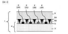
以下、本発明を実施するための形態の具体例を、図面に基づいて詳細に説明する。図1は、本発明のマイクロLEDディスプレイ装置の一態様を示す断面図である。マイクロLEDディスプレイ装置1は、複数のマイクロLED2が駆動基板3上に配列および実装されたマイクロLEDアレイ基板4と、マイクロLED2を区画する隔壁5と、マイクロLEDアレイ基板に対向する基板6を有する。マイクロLED2は、赤色マイクロLED2R、緑色マイクロLED2G、青色マイクロLED2Bをマトリクス状に配列したものであり、マイクロLEDディスプレイ装置1はフルカラー表示することができる。Specific examples of embodiments for carrying out the present invention will be described in detail below with reference to the drawings. FIG. 1 is a cross-sectional view showing one embodiment of a micro LED display device of the present invention. The micro
<マイクロLEDアレイ基板>
マイクロLEDとしては、例えば、赤色発光無機LED、緑色発光無機LED、青色発光無機LEDなどが挙げられる。マイクロLEDを構成する半導体材料としては、例えばInzGa1-zN(0<Z<1)、AlAs、GaAs、AlGaAs等が挙げられる。これらを2種以上用いてもよい。 <Micro LED array substrate>
Examples of micro-LEDs include red-emitting inorganic LEDs, green-emitting inorganic LEDs, and blue-emitting inorganic LEDs. Examples of semiconductor materials constituting micro-LEDs includeInzGa1-zN (0<Z<1), AlAs, GaAs, and AlGaAs. Two or more of these may be used.
各マイクロLEDは、マイクロLEDアレイ基板にマトリクス状に配列されることが好ましい。The micro LEDs are preferably arranged in a matrix on the micro LED array substrate.
各マイクロLEDは、外部に設けた駆動回路から駆動信号を供給し、それぞれ個別にオン及びオフ駆動して点灯及び消灯させる、すなわちスイッチ駆動するための配線を設けた駆動基板に接続されることが好ましい。It is preferable that each micro LED is connected to a drive board provided with wiring for switching on and off by supplying a drive signal from an external drive circuit and individually driving each micro LED to light up and light down.
<隔壁>
本発明における隔壁は、マイクロLEDディスプレイ装置の画素数に応じた繰り返しパターンを有することが好ましい。各マイクロLED間およびその周囲には、隔壁を有する。本発明における隔壁は、断面形状が、逆テーパー形状またはT字形状である遮光部を有し、遮光部の側面に反射部を有する。ここで、隔壁の断面形状とは、隔壁の厚み(高さ)方向に平行かつ隔壁の幅方向に平行な断面の形状を意味する。断面形状が逆テーパー形状またはT字形状である遮光部を有することにより、遮光性を向上させて、マイクロLEDおよび各画素発光部からの光漏れや各画素間の混色を抑制し、コントラストを向上させることができる。さらに、遮光部の側面に反射部を有することにより、マイクロLEDから隔壁方向に発光した光を反射して光の取り出し効率を高めることができ、輝度を向上させることができる。 <Bulkhead>
The partition wall in the present invention preferably has a repeating pattern according to the number of pixels of the micro LED display device. The partition wall is provided between and around each micro LED. The partition wall in the present invention has a light shielding portion having a cross-sectional shape of an inverse taper shape or a T-shape, and has a reflecting portion on the side of the light shielding portion. Here, the cross-sectional shape of the partition wall means a cross-sectional shape parallel to the thickness (height) direction of the partition wall and parallel to the width direction of the partition wall. By having a light shielding portion having a cross-sectional shape of an inverse taper shape or a T-shape, the light shielding property can be improved, and light leakage from the micro LED and each pixel light emitting portion and color mixing between each pixel can be suppressed, and contrast can be improved. Furthermore, by having a reflecting portion on the side of the light shielding portion, the light emitted from the micro LED toward the partition wall can be reflected to increase the light extraction efficiency, and the brightness can be improved.
隔壁の断面における逆テーパー形状またはT字形状の遮光部は、隣接する画素に対して略平行に、隔壁の厚み方向に位置する遮光層と、隔壁の幅方向に略平行に、隔壁上面に位置する遮光層を有することが好ましい。本明細書においては、前者を画素間遮光層、後者を上面遮光層と記載する場合がある。一般的に、マイクロLEDや、マイクロLEDの光によって励起して発光する波長変換層を含む画素部から放出される光は、全方向に放出されるため、一部の光は隔壁方向に放出される。そのため、隔壁方向に放出された光が隔壁を透過すると、隣接する他の画素部へ光漏れし、混色する課題が生じる。また、マイクロLEDは輝度が高く、隣接画素への光漏れおよび混色を抑制するためには、十分な遮光性が必要となる。このような課題に対して、隔壁内部に画素間遮光層を設けることにより、画素間光漏れを抑制することが可能となる。また、隔壁の光取出し方向側である上面に上面遮光層を有することにより、コントラストを向上させることができる。The light shielding portion having an inverse taper shape or a T-shape in the cross section of the partition preferably has a light shielding layer located in the thickness direction of the partition, approximately parallel to the adjacent pixels, and a light shielding layer located on the upper surface of the partition, approximately parallel to the width direction of the partition. In this specification, the former may be described as an inter-pixel light shielding layer, and the latter as an upper surface light shielding layer. Generally, light emitted from a pixel portion including a micro LED or a wavelength conversion layer excited by light from the micro LED and emitting light is emitted in all directions, so some of the light is emitted in the direction of the partition. Therefore, when light emitted in the direction of the partition passes through the partition, light leaks to other adjacent pixel portions, causing color mixing. In addition, micro LEDs have high brightness, and sufficient light shielding is required to suppress light leakage and color mixing to adjacent pixels. To address this issue, it is possible to suppress light leakage between pixels by providing an inter-pixel light shielding layer inside the partition. In addition, by having an upper surface light shielding layer on the upper surface of the partition, which is the light extraction direction side, contrast can be improved.
一方、遮光性の高い隔壁を設けると、前述したような画素部から放出される光を吸収するため、光取り出し効率が低下し、ディスプレイ装置としての輝度が低下する。本発明における隔壁構造は、画素間遮光層の側面に反射部を設けることにより、画素間遮光層や上面遮光層による効果を奏しながら、画素部から放出される光を反射して輝度を高めることができ、輝度とコントラストを向上させ、隣接画素間における光の混色を抑制することができる。On the other hand, if a partition with high light-shielding properties is provided, the light emitted from the pixel portion as described above will be absorbed, reducing the light extraction efficiency and the brightness of the display device. The partition structure of the present invention provides a reflective portion on the side of the inter-pixel light-shielding layer, thereby reflecting the light emitted from the pixel portion and increasing the brightness while still achieving the effects of the inter-pixel light-shielding layer and the top light-shielding layer, thereby improving the brightness and contrast and suppressing the mixing of light between adjacent pixels.
本発明における隔壁は、マイクロLEDディスプレイ装置の画素数に応じた繰り返しパターンを有することが好ましい。画素数としては、例えば、縦に4000個、横に2000個などが挙げられる。画素数は、表示される画像の解像度、すなわちきめ細かさに影響する。そのため、要求される画像の解像度と画像表示装置の画面サイズに応じた数の画素を形成するよう、隔壁のパターン形成寸法を選択することが好ましい。The partition wall of the present invention preferably has a repeating pattern according to the number of pixels of the micro LED display device. The number of pixels can be, for example, 4000 vertically and 2000 horizontally. The number of pixels affects the resolution, i.e., fineness, of the displayed image. Therefore, it is preferable to select the pattern formation dimensions of the partition wall so as to form a number of pixels according to the required image resolution and screen size of the image display device.
また、隔壁の厚みは、光源となる各マイクロLEDの厚みよりも大きいことが好ましく、具体的には、3μm~120μmが好ましい。In addition, the thickness of the partition is preferably greater than the thickness of each micro LED that serves as the light source, and specifically, is preferably 3 μm to 120 μm.
以下、遮光部と反射部とに分けて、図面を用いて詳細に説明する。The light-shielding section and the reflecting section will be explained in detail below with reference to the drawings.
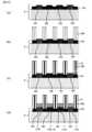
(遮光部)
図1に示すマイクロLEDディスプレイ装置1において、隔壁5は、断面形状が逆テーパー形状である遮光部5Aを有する。遮光部5Aは、厚み1.0μmあたりの光学濃度が0.1~4.0であることが好ましい。 (Light shielding part)
1, the
図4に、本発明における隔壁の断面形状の一態様を示す。図4における隔壁5は、逆テーパー形状の遮光部5Aを有する。図4における遮光部5Aの厚みは、側面に反射部5Bを有する部分(画素間遮光層)の長さLと、側面に反射部を持たない頂部(上面遮光層)の長さRに分解することができる。厚み1.0μmあたりの光学濃度を0.1以上とすることにより、遮光性をより向上させて光漏れや混色をより抑制することができる。厚み1.0μmあたりの光学濃度は、0.5以上がより好ましい。一方、厚み1.0μmあたりの光学濃度を4.0以下とすることにより、パターン加工性を向上させることができる。厚み1.0μmあたりの光学濃度は、3.0以下がより好ましい。遮光部5Aの光学濃度(OD値)は、光学濃度計(361T(visual);X-rite社製)を用いて入射光および透過光の強度を測定し、下記式(1)より算出することができる。
OD値 = log10(I0/I) ・・・ 式(1)
I0 : 入射光強度
I : 透過光強度。 FIG. 4 shows one embodiment of the cross-sectional shape of the partition wall in the present invention. The
OD value=log10(I0 /I) Equation (1)
I0 : Incident light intensity I: Transmitted light intensity.
なお、光学濃度を上記範囲にするための手段としては、例えば、遮光部5Aを後述する樹脂および黒色顔料を含有する組成とすることなどが挙げられる。In addition, one example of a means for achieving the optical density within the above range is to make the light-shielding
マイクロLED2から隣接画素へ光漏れする光の強度は、マイクロLED2から隔壁5へ入射する光の強度の1%以下に抑制することが好ましい。すなわち、遮光部5AのOD値は2以上であることが好ましい。It is preferable that the intensity of light leaking from the micro-LED 2 to an adjacent pixel be suppressed to 1% or less of the intensity of light incident on the
また、隔壁5の幅Wは、パターン加工性の観点から、3μm以上が好ましい。一方、隔壁5の幅Wは、マイクロLED2の発光領域を多く確保して輝度をより高める観点から、100μm以下であることが好ましい。隔壁5の厚みHは、マイクロLED2よりも厚い3μm以上が好ましい。The width W of the
遮光部5Aの厚みのうち、頂部(上面遮光層)の長さRは、遮光性を高め、高コントラストにすることで表示特性を向上させるために、0.5μm以上が好ましく、1.0μm以上がより好ましい。一方、遮光部5Aの頂部(上面遮光層)の長さRは、平坦性を向上させる観点から、10μm以下が好ましく、5μm以下がより好ましい。The length R of the top (upper light-shielding layer) of the light-shielding
また、隔壁5の側面における反射部5Bの厚みと遮光部5Aのうちの上面遮光層の厚み、すなわち図4に示すLとRの関係は、RよりもLのほうが大きいことが好ましい。In addition, the relationship between the thickness of the
また、遮光部5AのマイクロLEDアレイ基板に対して水平方向の長さを遮光部5Aの幅とすると、図4における遮光部5Aの幅は、最小値X1、最大値X2で表される。遮光部5Aの幅の最小値X1は、遮光性をより向上させて光漏れや混色をより抑制する観点から、0.5μm以上が好ましく、1.0μm以上がより好ましい。一方、遮光部5Aの幅の最小値X1は、反射部5Bの加工性の観点から、10μm以下が好ましく、5μm以下がより好ましい。また、遮光部5Aの幅の最大値X2は、1μm以上が好ましく、90μm以下が好ましい。If the horizontal length of the light-shielding
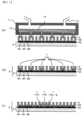
図5に、本発明における隔壁の断面形状の別の一態様を示す。図5における隔壁5は、T字形状の遮光部5Aを有する。図5における遮光部5Aの厚みは、側面に反射部5Bを有する部分(画素間遮光層)の長さLと、側面に反射部を持たない頂部(上面遮光層)の長さRに分解することができる。遮光部5Aの厚みのうち、頂部(上面遮光層)の長さRは、遮遮光性を高め、高コントラストにすることで表示特性を向上させるために、0.5μm以上が好ましく、1.0μm以上がより好ましい。一方、遮光部5Aの頂部(上面遮光層)の長さRは、平坦性を向上させる観点から、10μm以下が好ましく、5μm以下がより好ましい。Figure 5 shows another embodiment of the cross-sectional shape of the partition wall in the present invention. The
また、隔壁5の側面における反射部5Bの厚みと遮光部5Aのうちの上面遮光層の厚み、すなわち図5に示すLとRの関係は、RよりもLのほうが大きいことが好ましい。In addition, the relationship between the thickness of the
また、図5における遮光部5Aの幅は、X3で表される。遮光部5Aの幅X3は、遮光性をより向上させて光漏れや混色をより抑制する観点から、0.5μm以上が好ましく、1.0μm以上がより好ましい。一方、反射部5Bの加工性の観点から、10μm以下が好ましく、5μm以下がより好ましい。The width of the light-shielding
遮光部5Aは、樹脂および黒色顔料を含有することが好ましい。樹脂は、隔壁のクラック耐性および耐光性を向上させる機能を有する。黒色顔料は、入射した光を吸収し、射出光を低減する機能を有する。The light-shielding
樹脂としては、例えば、エポキシ樹脂、(メタ)アクリルポリマー、ポリウレタン、ポリエステル、ポリイミド、ポリオレフィン、ポリシロキサンなどが挙げられる。これらを2種以上含有してもよい。これらの中でも、耐熱性および溶媒耐性に優れることから、ポリイミドが好ましい。Examples of resins include epoxy resins, (meth)acrylic polymers, polyurethanes, polyesters, polyimides, polyolefins, polysiloxanes, etc. Two or more of these may be contained. Among these, polyimides are preferred because of their excellent heat resistance and solvent resistance.
黒色顔料としては、例えば、黒色有機顔料、混色有機顔料、無機顔料等が挙げられる。黒色有機顔料としては、例えば、カーボンブラック、ペリレンブラック、アニリンブラック、ベンゾフラノン系顔料などが挙げられる。これらは、樹脂で被覆されていてもよい。混色有機顔料としては、例えば、赤、青、緑、紫、黄色、マゼンダおよび/またはシアン等の2種以上の顔料を混合して疑似黒色化したものが挙げられる。黒色無機顔料としては、例えば、グラファイト;チタン、銅、鉄、マンガン、コバルト、クロム、ニッケル、亜鉛、カルシウム、銀等の金属の微粒子;金属酸化物;金属複合酸化物;金属硫化物;金属窒化物;金属酸窒化物;金属炭化物などが挙げられる。Examples of black pigments include black organic pigments, mixed-color organic pigments, and inorganic pigments. Examples of black organic pigments include carbon black, perylene black, aniline black, and benzofuranone-based pigments. These may be coated with resin. Examples of mixed-color organic pigments include pseudo-black pigments made by mixing two or more pigments such as red, blue, green, purple, yellow, magenta, and/or cyan. Examples of black inorganic pigments include graphite; fine particles of metals such as titanium, copper, iron, manganese, cobalt, chromium, nickel, zinc, calcium, and silver; metal oxides; metal composite oxides; metal sulfides; metal nitrides; metal oxynitrides; and metal carbides.
(反射部)
図1に示すマイクロLEDディスプレイ装置1において、隔壁5は、遮光部5Aの側面に反射部5Bを有する。反射部5Bは、波長550nmにおける厚み10μmあたりの反射率が40~90%であることが好ましい。ここで、反射部5Bの厚みとは、マイクロLEDアレイ基板に対して垂直方向(図1の上下方向)の反射部5Bの長さを指す。 (Reflective part)
In the micro
図4における反射部5Bは、逆テーパー形状の凸部を有する凹構造を有し、図4における反射部5Bの厚みは、反射部5Bの長さLで表される。波長550nmにおける厚み10μmあたりの反射率を40%以上とすることにより、隔壁5側面における反射により輝度をより向上させることができる。波長550nmにおける厚み10μmあたりの反射率は、70%以上がより好ましい。一方、波長550nmにおける厚み10μmあたりの反射率を90%以下とすることにより、パターン形成精度を向上させることができる。反射部5Bの波長550nmにおける厚み10μmあたりの反射率は、厚み10μmの反射部5Bについて、上面から分光測色計(例えば、コニカミノルタ(株)製CM-2600d)を用いて、SCIモードにより測定することができる。ただし、測定に十分な面積を確保できない場合や、厚み10μmの測定サンプルが採取できない場合において、反射部5Bの組成が既知である場合には、反射部5Bと同組成の厚み10μmのベタ膜を作製し、反射部5Bに代えて、該ベタ膜について反射率を測定してもよい。例えば、反射部5Bを形成した材料を用いて、厚みを10μmとし、パターン形成しないこと以外は反射部5Bの形成と同じ加工条件によりベタ膜を作製し、得られたベタ膜について、上面から、同様に反射率を測定してもよい。The
なお、反射率を上記範囲にするための手段としては、例えば、反射部5Bを後述する樹脂および白色顔料を含有する組成とすることなどが挙げられる。One way to achieve a reflectance within the above range is to make the
反射部5Bの厚みLは、3~120μmが好ましい。The thickness L of the
また、図4において、反射部5BのマイクロLEDアレイ基板に対して水平方向の長さ、すなわち反射部5Bの幅は、最小値Y1、最大値Y2で表される。反射部5Bの幅の最小値Y1は、0.5~20μmが好ましい。また、最大値Y2は1~40μmが好ましい。In addition, in FIG. 4, the horizontal length of the
図5に、本発明における隔壁の断面形状の別の一態様を示す。図5における隔壁5は、中央に空洞を有する反射部5Bを有する。図5における遮光部5Bの厚みは、反射部5Bの長さLで表される。反射部5Bの厚みLは、3~120μmが好ましい。Figure 5 shows another embodiment of the cross-sectional shape of the partition wall in the present invention. The
また、図5における反射部5Bの幅は、Y3で表される。反射部5Bの幅Y3は、0.5~40μmが好ましい。The width of the
なお、本発明において、一つの隔壁5の断面に対して、反射部5Bは遮光部5Aを挟んで両側に存在する。図4および図5においては説明を簡略化するために遮光部5Aを挟んだ両側の反射部の寸法は同一として記載するが、反射部5Bの寸法は遮光部5Aを挟んで非対称でもよい。In the present invention, the
反射部5Bは、樹脂および白色顔料を含有することが好ましい。樹脂は、隔壁のクラック耐性および耐光性を向上させる機能を有する。白色顔料は、反射部5Bの反射率を向上させる機能を有する。例えば、樹脂、白色顔料、光重合開始剤、光重合性化合物および有機溶媒を含有する感光性着色組成物を用いることにより、高い反射率を有し、厚膜化しても高い解像度を有する反射部を形成することができる。The
樹脂としては、遮光部5Aを構成する樹脂として例示したものが挙げられる。耐熱性に優れることから、ポリイミドおよびポリシロキサンが好ましい。Examples of resins include those exemplified as resins constituting the light-shielding
白色顔料としては、例えば、二酸化チタン、酸化ジルコニウム、酸化亜鉛、硫酸バリウム、これらの複合化合物などが挙げられる。これらを2種以上含有してもよい。これらの中でも、反射率が高く工業的利用が容易な二酸化チタンが好ましい。二酸化チタンの結晶構造は、アナターゼ型、ルチル型、ブルッカイト型に分類される。これらの中でも、光触媒活性が低いことから、ルチル型酸化チタンが好ましい。Examples of white pigments include titanium dioxide, zirconium oxide, zinc oxide, barium sulfate, and composite compounds of these. Two or more of these may be contained. Of these, titanium dioxide is preferred because it has a high reflectance and is easy to use industrially. The crystal structure of titanium dioxide is classified into anatase type, rutile type, and brookite type. Of these, rutile type titanium oxide is preferred because it has low photocatalytic activity.
<マイクロLEDアレイ基板に対向する基板>
本発明におけるマイクロLEDアレイ基板に対向する基板としては、例えば、ガラス板、樹脂板、樹脂フイルムなどが挙げられる。ガラス板の材質としては、無アルカリガラスが好ましい。樹脂板および樹脂フイルムの材質としては、ポリエステル、(メタ)アクリルポリマー、透明ポリイミド、ポリエーテルスルフォン等が好ましい。ガラス板および樹脂板の厚みは、1mm以下が好ましく、0.8mm以下が好ましい。樹脂フイルムの厚みは、100μm以下が好ましい。 <Substrate facing the micro LED array substrate>
Examples of the substrate facing the micro LED array substrate in the present invention include a glass plate, a resin plate, and a resin film. The material of the glass plate is preferably alkali-free glass. The material of the resin plate and the resin film is preferably polyester, (meth)acrylic polymer, transparent polyimide, polyethersulfone, and the like. The thickness of the glass plate and the resin plate is preferably 1 mm or less, and preferably 0.8 mm or less. The thickness of the resin film is preferably 100 μm or less.
図2は、本発明のマイクロLEDディスプレイ装置の別の一態様を示す断面図である。マイクロLEDディスプレイ装置1は、複数のマイクロLED2が駆動基板3上に配列および実装されたマイクロLEDアレイ基板4と、マイクロLED2の上部の波長変換層7および/または光散乱層8と、マイクロLED2を区画する隔壁5と、マイクロLEDアレイ基板に対向する基板6を有する。図2においては、マイクロLED2は単一色であり、波長変換層7によりマイクロLED2の発光を色変換し、フルカラー表示することができる。図2に示すマイクロLEDディスプレイ装置1の基本構成は図1に示すマイクロLEDディスプレイ装置1と同様である。Figure 2 is a cross-sectional view showing another embodiment of the micro LED display device of the present invention. The micro
<マイクロLEDアレイ基板>
本実施形態は、マイクロLEDを光源として、光源からの光により励起される波長変換層を有する構成を有するマイクロLEDディスプレイ装置である。波長変換層における波長変換材料を励起する光源としては、紫外光、青色光が好ましく、マイクロLEDとしては、紫外マイクロLED、青色マイクロLEDなどが挙げられる。紫外から青色波長帯の光を放射する、窒化ガリウム(GaN)を主材料するマイクロLEDが好ましい。例えば、波長200nm~380nmの近紫外線を放射する紫外マイクロLEDであってもよいし、波長380nm~500nmの青色光を放射する青色マイクロLEDであってもよい。 <Micro LED array substrate>
The present embodiment is a micro-LED display device having a configuration in which a wavelength conversion layer is excited by light from a micro-LED as a light source. The light source for exciting the wavelength conversion material in the wavelength conversion layer is preferably ultraviolet light or blue light, and examples of the micro-LED include ultraviolet micro-LEDs and blue micro-LEDs. A micro-LED that emits light in the ultraviolet to blue wavelength range and is mainly made of gallium nitride (GaN) is preferred. For example, it may be an ultraviolet micro-LED that emits near-ultraviolet light with a wavelength of 200 nm to 380 nm, or a blue micro-LED that emits blue light with a wavelength of 380 nm to 500 nm.
<波長変換層>
本実施形態において、赤色画素部および緑色画素部は、マイクロLED2からの励起光を吸収し、赤色、緑色を発光する波長変換物質を含有する波長変換層7から構成される。また、青色画素部は、マイクロLED2からの励起光を吸収し、青色を発光する波長変換物質を含有する波長変換層7および/または光散乱層8から構成される。 Wavelength Conversion Layer
In this embodiment, the red pixel portion and the green pixel portion are composed of a
各画素のON/OFFは、マイクロLEDのON/OFFにより行う。紫外マイクロLEDを用いる場合、波長変換層の赤色画素部7Rには、紫外線により励起されて赤色の蛍光を発する赤色波長変換材料を含有することが好ましく、波長変換層の緑色画素部7Gには、紫外線により励起されて緑色の蛍光を発する緑色波長変換物質を含有することが好ましく、波長変換層の青色画素部7Bには、紫外線により励起されて青色の蛍光を発する青色波長変換物質を含有することが好ましい。また、青色マイクロLEDを用いる場合、波長変換層の赤色画素部7Rには、青色励起光により励起されて赤色の蛍光を発する赤色波長変換物質を含有することが好ましく、波長変換層の緑色画素部7Gには、青色励起光により励起されて緑色の蛍光を発する緑色波長変換物質を含有することが好ましく、波長変換層の青色画素部7Bには、指向性を有する励起光を散乱して等方発光に変換して外部へ取り出し可能となる光散乱性物質を含有した光散乱層8が形成されることが好ましい。また、図2において、各色対応の波長変換層は、ストライプ状に設けても、各LEDに個別に対応させて設けてもよい。Each pixel is turned on/off by turning on/off the micro LED. When an ultraviolet micro LED is used, the
波長変換層7は、無機蛍光体および/または有機蛍光体を含有することが好ましい。無機蛍光体は、発光スペクトルのピーク波長により、緑色や赤色などの各色を発光する。無機蛍光体としては、波長400~500nmの励起光により励起され、発光スペクトルが500~700nmの領域にピークを有するものや、量子ドットと称される無機半導体微粒子などが挙げられる。これらの中でも、無機蛍光体が好ましい。無機蛍光体の形状としては、例えば、球状、柱状などが挙げられる。かかる無機蛍光体としては、例えば、YAG系蛍光体、TAG系蛍光体、サイアロン系蛍光体、Mn4+付活フッ化物錯体蛍光体等が挙げられるが特に限定されない。また、これらを2種以上用いてもよい。例えば、赤色では、Y2O3:Eu、YVO4:Eu、(Y,Gd)BO3:Eu、Y(P,V)O4:Eu、Y2O3S:Eu、などがあげられる。緑色では、Zn2GeO2:Mn、BaAl12O19:Mn、Zn2SiO4:Mn、Zn2SiO4:Mn,As、Y3Al5O12:Ce、Gd2O2S:Tb、などがあげられる。青色では、BaMgAl14O23:Eu、BaMgAl16O27:Eu、BaMg2Al14O24:Eu、Y2SiO3:Ceなどがあげられる。中でも、組成式Y1-aEuaTaO4(式中、aは、0.005~0.1である)で表されるユーロピウム付活タンタル酸イットリウム蛍光体が好ましく挙げられる。赤色蛍光体には、ユーロピウム付活ホウ酸イットリウムガドリニウムやユーロピウム付活燐酸バナジン酸イットリウムなどが好ましく用いられ、緑色蛍光体には、組成式Y1-bTbbTaO4(式中、bは、0.001~0.2である)で表されるテルビウム付活タンタル酸イットリウムが好ましく用いられる。また、青色蛍光体には、Y1-cTmcTaO4(式中、cは、0.001~0.2である)で表されるツリウム付活タンタル酸イットリウムが好ましく用いられる。 The
さらに、量子ドットがより好ましい。量子ドットは他の蛍光体と比較して平均粒子径が小さいことから、波長変換発光材料を含有する層の表面を平滑化して表面における光散乱を抑制することができるため、光の取り出し効率をより向上させ、輝度をより向上させることができる。Furthermore, quantum dots are more preferable. Since quantum dots have a smaller average particle size than other phosphors, they can smooth the surface of the layer containing the wavelength conversion luminescent material and suppress light scattering on the surface, thereby further improving the light extraction efficiency and brightness.
量子ドットの材料としては、例えば、II-IV族、III-V族、IV-VI族、IV族の半導体などが挙げられる。これらの無機半導体としては、例えば、Si、Ge、Sn、Se、Te、B、C(ダイアモンドを含む)、P、BN、BP、BAs、AlN、AlP、AlAs、AlSb、GaN、GaP、GaAs、GaSb、InN、InP、InAs、InSb、ZnO、ZnS、ZnSe、ZnTe、CdS、CdSe、CdSeZn、CdTe、HgS、HgSe、HgTe、BeS、BeSe、BeTe、MgS、MgSe、GeS、GeSe、GeTe、SnS、SnSe、SnTe、PbO、PbS、PbSe、PbTe、CuF、CuCl、CuBr、CuI、Si3N4、Ge3N4、Al2O3などが挙げられる。これらを2種以上用いてもよい。 Examples of quantum dot materials include Group II-IV, Group III-V, Group IV-VI, and Group IV semiconductors. Examples of these inorganic semiconductors include Si, Ge, Sn, Se, Te, B, C (including diamond), P, BN, BP, BAs, AlN, AlP, AlAs, AlSb, GaN, GaP, GaAs, GaSb, InN, InP, InAs, InSb, ZnO, ZnS, ZnSe, ZnTe, CdS, CdSe, CdSeZn, CdTe, HgS, HgSe, HgTe, BeS, BeSe, BeTe, MgS, MgSe, GeS, GeSe, GeTe, SnS, SnSe, SnTe, PbO, PbS, PbSe, PbTe, CuF, CuCl, CuBr, CuI,Si3N4 ,Ge3N4 ,andAl2O.3. Two or more of these may be used.
量子ドットは、p型ドーパントまたはn型ドーパントを含有してもよい。また、量子ドットは、コアシェル構造を有してもよい。コアシェル構造においては、シェルの周囲に目的に応じて任意の適切な機能層(単一層または複数層)が形成されていてもよく、シェル表面に表面処理および/または化学修飾がなされていてもよい。The quantum dots may contain a p-type dopant or an n-type dopant. The quantum dots may have a core-shell structure. In the core-shell structure, any suitable functional layer (single layer or multiple layers) may be formed around the shell depending on the purpose, and the shell surface may be surface-treated and/or chemically modified.
量子ドットの形状としては、例えば、球状、柱状、燐片状、板状、不定形等が挙げられる。量子ドットの平均粒子径は、所望の発光波長に応じて選択することができ、1~30nmが好ましい。量子ドットの平均粒子径が1~10nmであれば、青色、緑色および赤色のそれぞれにおいて、発光スペクトルにおけるピークをよりシャープにすることができる。例えば、量子ドットの平均粒子径が約2nmの場合には青色光を、約3nmの場合には緑色光を、約6nmの場合には赤色光を発光する。量子ドットの平均粒子径は2nm以上が好ましく、8nm以下が好ましい。量子ドットの平均粒子径は、動的光散乱法により測定することができる。平均粒子径の測定装置としては、ダイナミック光散乱光度計DLS-8000(大塚電子(株)製)などが挙げられる。The shape of the quantum dots can be, for example, spherical, columnar, scaly, plate-like, amorphous, etc. The average particle size of the quantum dots can be selected according to the desired emission wavelength, and is preferably 1 to 30 nm. If the average particle size of the quantum dots is 1 to 10 nm, the peaks in the emission spectrum can be made sharper in each of blue, green, and red. For example, when the average particle size of the quantum dots is about 2 nm, blue light is emitted, when it is about 3 nm, green light is emitted, and when it is about 6 nm, red light is emitted. The average particle size of the quantum dots is preferably 2 nm or more, and preferably 8 nm or less. The average particle size of the quantum dots can be measured by dynamic light scattering. An example of an average particle size measuring device is the dynamic light scattering photometer DLS-8000 (manufactured by Otsuka Electronics Co., Ltd.).
有機蛍光体としては、例えば、青色の励起光により励起され赤色および緑色の蛍光を発する蛍光体として、ピロメテン系誘導体などが挙げられる。その他には、置換基の選択により赤色または緑色の蛍光を発するペリレン系誘導体、ポルフィリン系誘導体、オキサジン系誘導体、ピラジン系誘導体などが挙げられる。これらを2種以上含有してもよい。これらの中でも、量子収率が高いことから、ピロメテン誘導体が好ましい。ピロメテン誘導体は、例えば、特開2011-241160号公報に記載の方法により得ることができる。As an example of an organic fluorescent material, pyrromethene derivatives can be mentioned as a fluorescent material that is excited by blue excitation light and emits red and green fluorescence. Other examples include perylene derivatives, porphyrin derivatives, oxazine derivatives, and pyrazine derivatives that emit red or green fluorescence depending on the selection of the substituent. Two or more of these may be contained. Among these, pyrromethene derivatives are preferred because of their high quantum yield. Pyrromethene derivatives can be obtained, for example, by the method described in JP 2011-241160 A.
波長変換層は、前記無機蛍光体および/または有機蛍光体をバインダー樹脂に分散させ、波長変換ペーストとしてパターン加工することで形成できる。バインダー樹脂として、例えば、ポリビニルアセテート、ポリビニルアルコール、エチルセルロース、メチルセルロース、ポリエチレン、ポリメチルシロキサン若しくはポリメチルフェニルシロキサン等のシリコン樹脂、ポリスチレン、ブタジエン/スチレンコポリマー、ポリスチレン、ポリビニルピロリドン、ポリアミド、高分子量ポリエーテル、エチレンオキサイドとプロピレンオキサイドとの共重合体、ポリアクリルアミド又はアクリル樹脂などが好ましく挙げられる。これらの樹脂の中でも、セルロース系ポリマーを使用することが好ましい。波長変換層は、波長変換ペーストを硬化させて形成することが好ましい。波長変換ペーストを硬化させる方法は特に限定されないが、重合性化合物を含有する波長変換ペーストを熱や光で硬化させる方法や、溶媒を含有する波長変換ペーストから加熱により溶媒を揮発させて硬化させる方法などが挙げられる。波長変換ペーストは、上記の必須成分に加え、モノマー、重合開始剤、溶媒、分散剤などを適宜含んでいても良い。The wavelength conversion layer can be formed by dispersing the inorganic phosphor and/or organic phosphor in a binder resin and patterning the resulting wavelength conversion paste. Examples of the binder resin include silicon resins such as polyvinyl acetate, polyvinyl alcohol, ethyl cellulose, methyl cellulose, polyethylene, polymethyl siloxane, and polymethylphenyl siloxane, polystyrene, butadiene/styrene copolymers, polystyrene, polyvinylpyrrolidone, polyamide, high molecular weight polyether, copolymers of ethylene oxide and propylene oxide, polyacrylamide, and acrylic resins. Among these resins, it is preferable to use a cellulose-based polymer. The wavelength conversion layer is preferably formed by curing the wavelength conversion paste. The method for curing the wavelength conversion paste is not particularly limited, but examples include a method of curing a wavelength conversion paste containing a polymerizable compound with heat or light, and a method of curing a wavelength conversion paste containing a solvent by volatilizing the solvent by heating. In addition to the above essential components, the wavelength conversion paste may also contain a monomer, a polymerization initiator, a solvent, a dispersant, and the like as appropriate.
モノマーとしては、分子中にエチレン性不飽和二重結合を有する化合物であることが好ましい。モノマーは、分子中に2つ以上のエチレン性不飽和二重結合を有することが好ましい。モノマーとしては、例えば、ジエチレングリコールジアクリレート、トリエチレングリコールジアクリレート、テトラエチレングリコールジアクリレート、ポリエチレングリコールジアクリレート、ジプロピレングリコールジアクリレート、トリプロピレングリコールジアクリレート、ポリプロピレングリコールジアクリレート、ジエチレングリコールジメタクリレート、トリエチレングリコールジメタクリレート、テトラエチレングリコールジメタクリレート、ポリプロピレングリコールジメタクリレート、トリメチロールプロパンジアクリレート、トリメチロールプロパントリアクリレート、トリメチロールプロパンジメタクリレート、トリメチロールプロパントリメタクリレート、1,3-ブタンジオールジアクリレート、1,3-ブタンジオールジメタクリレート、ネオペンチルグリコールジアクリレート、1,4-ブタンジオールジアクリレート、1,4-ブタンジオールジメタクリレート、1,6-ヘキサンジオールジアクリレート、1,9-ノナンジオールジメタクリレート、1,10-デカンジオールジメタクリレート、ジメチロール-トリシクロデカンジアクリレート、ペンタエリスリトールトリアクリレート、ペンタエリスリトールテトラアクリレート、ペンタエリスリトールトリメタクリレート、ペンタエリスリトールテトラメタクリレート、ジペンタエリスリトールペンタアクリレート、ジペンタエリスリトールヘキサアクリレート、トリペンタエリスリトールヘプタアクリレート、トリペンタエリスリトールオクタアクリレート、テトラペンタエリスリトールノナアクリレート、テトラペンタエリスリトールデカアクリレート、ペンタペンタエリスリトールウンデカアクリレート、ペンタペンタエリスリトールドデカアクリレート、トリペンタエリスリトールヘプタメタクリレート、トリペンタエリスリトールオクタメタクリレート、テトラペンタエリスリトールノナメタクリレート、テトラペンタエリスリトールデカメタクリレート、ペンタペンタエリスリトールウンデカメタクリレート、ペンタペンタエリスリトールドデカメタクリレート、ジメチロール-トリシクロデカンジアクリレート等が挙げられる。これらを2種以上含有してもよい。波長変換ペースト中におけるモノマーの含有量は、波長変換ペーストの固形分率を高める観点から、固形分中、1重量%以上が好ましく、10重量%以上がより好ましく、30重量%以上がさらにより好ましい。一方、ノズルからの吐出を安定化させる観点から、モノマーの含有量は、固形分中、80重量%以下が好ましく、70重量%以下がより好ましい。波長変換ペーストに重合開始剤を含む場合には、例えば、ラジカル開始剤やカチオン開始剤、すなわち、光(紫外線、電子線を含む)、または熱により反応し、ラジカルやカチオンなどの活性種を発生させるものであればどのようなものでもよい。これらの中でも、ラジカル開始剤であることが好ましい。重合開始剤としては、例えば、2-メチル-[4-(メチルチオ)フェニル]-2-モルフォリノプロパン-1-オン、2-ジメチルアミノ-2-(4-メチルベンジル)-1-(4-モルフォリン-4-イル-フェニル)-ブタン-1-オン、2-ベンジル-2-ジメチルアミノ-1-(4-モルフォリノフェニル)-ブタノン-1などのα-アミノアルキルフェノン化合物;2,4,6-トリメチルベンゾイルフェニルホスフィンオキサイド、ビス(2,4,6-トリメチルベンゾイル)-フェニルホスフィンオキサイド、ビス(2,6-ジメトキシベンゾイル)-(2,4,4-トリメチルペンチル)-ホスフィンオキサイドなどのアシルホスフィンオキサイド化合物;1-フェニル-1,2-プロパンジオン-2-(O-エトキシカルボニル)オキシム、1-[4-(フェニルチオ)フェニル]オクタン-1,2-ジオン=2-(O-ベンゾイルオキシム)]、1-フェニル-1,2-ブタジオン-2-(O-メトキシカルボニル)オキシム、1,3-ジフェニルプロパントリオン-2-(O-エトキシカルボニル)オキシム、エタノン,1-[9-エチル-6-(2-メチルベンゾイル)-9H-カルバゾール-3-イル]-,1-(O-アセチルオキシム)などのオキシムエステル化合物;ベンジルジメチルケタールなどのベンジルケタール化合物;2-ヒドロキシ-2-メチル-1-フェニルプロパン-1-オン、1-(4-イソプロピルフェニル)-2-ヒドロキシ-2-メチルプロパン-1-オン、4-(2-ヒドロキシエトキシ)フェニル-(2-ヒドロキシ-2-プロピル)ケトン、1-ヒドロキシシクロヘキシル-フェニルケトンなどのα-ヒドロキシケトン化合物;ベンゾフェノン、4,4-ビス(ジメチルアミノ)ベンゾフェノン、4,4-ビス(ジエチルアミノ)ベンゾフェノン、O-ベンゾイル安息香酸メチル、4-フェニルベンゾフェノン、4,4-ジクロロベンゾフェノン、ヒドロキシベンゾフェノン、4-ベンゾイル-4’-メチル-ジフェニルサルファイド、アルキル化ベンゾフェノン、3,3’,4,4’-テトラ(t-ブチルパーオキシカルボニル)ベンゾフェノンなどのベンゾフェノン化合物;2,2-ジエトキシアセトフェノン、2,3-ジエトキシアセトフェノン、4-t-ブチルジクロロアセトフェノン、ベンザルアセトフェノン、4-アジドベンザルアセトフェノンなどのアセトフェノン化合物;2-フェニル-2-オキシ酢酸メチルなどの芳香族ケトエステル化合物;4-ジメチルアミノ安息香酸エチル、4-ジメチルアミノ安息香酸(2-エチル)ヘキシル、4-ジエチルアミノ安息香酸エチル、2-ベンゾイル安息香酸メチルなどの安息香酸エステル化合物などが挙げられる。これらを2種以上含有してもよい。The monomer is preferably a compound having an ethylenically unsaturated double bond in the molecule. The monomer preferably has two or more ethylenically unsaturated double bonds in the molecule. Examples of the monomer include diethylene glycol diacrylate, triethylene glycol diacrylate, tetraethylene glycol diacrylate, polyethylene glycol diacrylate, dipropylene glycol diacrylate, tripropylene glycol diacrylate, polypropylene glycol diacrylate, diethylene glycol dimethacrylate, triethylene glycol dimethacrylate, tetraethylene glycol dimethacrylate, polypropylene glycol dimethacrylate, trimethylolpropane diacrylate, trimethylolpropane triacrylate, trimethylolpropane dimethacrylate, trimethylolpropane trimethacrylate, 1,3-butanediol diacrylate, 1,3-butanediol dimethacrylate, neopentyl glycol diacrylate, 1,4-butanediol diacrylate, 1,4-butanediol dimethacrylate, 1,6-hexanediol diacrylate, 1,9-nonanediol dimethacrylate, 1,10-decanediol dimethacrylate, 1,2-decanediol dimethacrylate, 1,3-decanediol dimethacrylate, 1,4-dec ...10-decanediol dimethacrylate, 1,2-decanediol dimethacrylate, 1,3-decanediol dimethacrylate, 1,4-decanediol dimethacrylate, 1,6-decanediol dimethacrylate, 1,9-decanediol dimethacrylate, 1,10-decanediol dimethacrylate, 1,10-decanediol dimethacrylate, 1,10-decanediol dimethacrylate, 1,2-decanediol dimethacrylate, 1,3-decanediol dimethacrylate, 1,4- Methacrylate, dimethylol-tricyclodecane diacrylate, pentaerythritol triacrylate, pentaerythritol tetraacrylate, pentaerythritol trimethacrylate, pentaerythritol tetramethacrylate, dipentaerythritol pentaacrylate, dipentaerythritol hexaacrylate, tripentaerythritol heptaacrylate, tripentaerythritol octaacrylate, tetrapentaerythritol nonaacrylate, tetrapentaerythritol decaacrylate, pentapentaerythritol undecaacrylate, pentapentaerythritol dodecaacrylate, tripentaerythritol heptamethacrylate, tripentaerythritol octamethacrylate, tetrapentaerythritol nonamethacrylate, tetrapentaerythritol decamethacrylate, pentapentaerythritol undecamethacrylate, pentapentaerythritol dodecamethacrylate, dimethylol-tricyclodecane diacrylate, and the like. Two or more of these may be contained. The content of the monomer in the wavelength conversion paste is preferably 1% by weight or more, more preferably 10% by weight or more, and even more preferably 30% by weight or more, based on the solid content, from the viewpoint of increasing the solid content rate of the wavelength conversion paste. On the other hand, the content of the monomer is preferably 80% by weight or less, more preferably 70% by weight or less, based on the solid content, from the viewpoint of stabilizing the ejection from the nozzle. When the wavelength conversion paste contains a polymerization initiator, it may be, for example, a radical initiator or a cationic initiator, that is, any initiator that reacts with light (including ultraviolet rays and electron beams) or heat to generate active species such as radicals and cations. Among these, a radical initiator is preferable. Examples of the polymerization initiator include α-aminoalkylphenone compounds such as 2-methyl-[4-(methylthio)phenyl]-2-morpholinopropan-1-one, 2-dimethylamino-2-(4-methylbenzyl)-1-(4-morpholin-4-yl-phenyl)-butan-1-one, and 2-benzyl-2-dimethylamino-1-(4-morpholinophenyl)-butanone-1; 2,4,6-trimethylbenzoylphenylphosphine oxide, bis(2,4,6-trimethylbenzoyl)-phenylphosphine oxide, and bis(2,6-dimethoxybenzoyl)-(2,4,4-trimethylpentyl)-phosphine oxide. acylphosphine oxide compounds such as 1-phenyl-1,2-propanedione-2-(O-ethoxycarbonyl)oxime, 1-[4-(phenylthio)phenyl]octane-1,2-dione=2-(O-benzoyloxime)], 1-phenyl-1,2-butadione-2-(O-methoxycarbonyl)oxime, 1,3-diphenylpropanetrione-2-(O-ethoxycarbonyl)oxime, ethanone, 1-[9-ethyl-6-(2-methylbenzoyl)-9H-carbazol-3-yl]-, 1-(O-acetyloxime) and other oxime ester compounds; benzil ketal compounds such as benzil dimethyl ketal; 2-hydroxyphenyl ketal compounds such as 1-phenyl-1,2-propanedione-2-(O-ethoxycarbonyl)oxime, 1-phenyl-1,2-butadione-2-(O-methoxycarbonyl)oxime, 1,3-diphenylpropanetrione-2-(O-ethoxycarbonyl)oxime, ethanone, 1-[9-ethyl-6-(2-methylbenzoyl)-9H-carbazol-3-yl]-, 1-(O-acetyloxime) and other oxime ester compounds; α-hydroxyketone compounds such as 4-(2-hydroxyethoxy)phenyl-(2-hydroxy-2-propyl)ketone, and 1-hydroxycyclohexyl-phenyl ketone; benzophenone, 4,4-bis(dimethylamino)benzophenone, 4,4-bis(diethylamino)benzophenone, methyl O-benzoylbenzoate, 4-phenylbenzophenone, 4,4-dichlorobenzophenone, hydroxybenzophenone, 4-benzoyl-4'-methyl-diphenyl sulfide, and arsenic compounds; Benzophenone compounds such as alkylated benzophenone and 3,3',4,4'-tetra(t-butylperoxycarbonyl)benzophenone; acetophenone compounds such as 2,2-diethoxyacetophenone, 2,3-diethoxyacetophenone, 4-t-butyldichloroacetophenone, benzalacetophenone, and 4-azidobenzalacetophenone; aromatic ketoester compounds such as methyl 2-phenyl-2-oxyacetate; benzoic acid ester compounds such as ethyl 4-dimethylaminobenzoate, (2-ethyl)hexyl 4-dimethylaminobenzoate, ethyl 4-diethylaminobenzoate, and methyl 2-benzoylbenzoate. Two or more of these may be included.
波長変換ペーストは。重合開始剤による着色を抑制するため、2,4,6-トリメチルベンゾイルフェニルホスフィンオキサイド、ビス(2,4,6-トリメチルベンゾイル)-フェニルホスフィンオキサイド、ビス(2,6-ジメトキシベンゾイル)-(2,4,4-トリメチルペンチル)-ホスフィンオキサイド等のアシルホスフィンオキサイド系重合開始剤を含むことが好ましい。波長変換ペースト中における重合開始剤の含有量は、ラジカル硬化を効率的に進める観点から、固形分中、0.01重量%以上が好ましく、0.1重量%以上がより好ましい。一方、残留した重合開始剤の溶出等を抑制し、黄変をより抑制させる観点から、重合開始剤の含有量は、固形分中、20重量%以下が好ましく、10重量%以下がより好ましい。The wavelength conversion paste preferably contains an acylphosphine oxide-based polymerization initiator such as 2,4,6-trimethylbenzoylphenylphosphine oxide, bis(2,4,6-trimethylbenzoyl)-phenylphosphine oxide, or bis(2,6-dimethoxybenzoyl)-(2,4,4-trimethylpentyl)-phosphine oxide, in order to suppress coloration caused by the polymerization initiator. The content of the polymerization initiator in the wavelength conversion paste is preferably 0.01% by weight or more, and more preferably 0.1% by weight or more, based on the solid content, in order to efficiently promote radical curing. On the other hand, in order to suppress elution of the remaining polymerization initiator and to further suppress yellowing, the content of the polymerization initiator is preferably 20% by weight or less, and more preferably 10% by weight or less, based on the solid content.
波長変換ペーストに溶媒を含む場合には、例えば、メタノール、エタノール、プロパノール、イソプロパノール、ブタノール、イソブタノール、t-ブタノール、ペンタノール、4-メチル-2-ペンタノール、3-メチル-2-ブタノール、3-メチル-3-メトキシ-1-ブタノール、ジアセトンアルコールなどのアルコール類;エチレングリコール、プロピレングリコールなどのグリコール類;エチレングリコールモノメチルエーテル、エチレングリコールモノエチルエーテル、プロピレングリコールモノメチルエーテル、プロピレングリコールモノエチルエーテル、プロピレングリコールモノプロピルエーテル、プロピレングリコールモノブチルエーテル、プロピレングリコールモノ-t-ブチルエーテル、エチレングリコールジメチルエーテル、エチレングリコールジエチルエーテル、エチレングリコールジブチルエーテル、ジエチルエーテルなどのエーテル類;メチルエチルケトン、アセチルアセトン、メチルプロピルケトン、メチルブチルケトン、メチルイソブチルケトン、ジイソブチルケトン、シクロペンタノン、2-ヘプタノンなどのケトン類;ジメチルホルムアミド、ジメチルアセトアミドなどのアミド類;エチルアセテート、プロピルアセテート、ブチルアセテート、イソブチルアセテート、エチレングリコールモノエチルエーテルアセテート、プロピレングリコールモノメチルエーテルアセテート、3-メトキシブチルアセテート、3-メチル-3-メトキシブチルアセテート、乳酸メチル、乳酸エチル、乳酸ブチルなどのアセテート類;トルエン、キシレン、ヘキサン、シクロヘキサンなどの芳香族または脂肪族炭化水素;γ-ブチロラクトン、N-メチル-2-ピロリドン、ジメチルスルホキシドなどが好ましく挙げられる。このうち、前記溶媒が、アセテート類であるのがさらに好ましい。When the wavelength conversion paste contains a solvent, for example, alcohols such as methanol, ethanol, propanol, isopropanol, butanol, isobutanol, t-butanol, pentanol, 4-methyl-2-pentanol, 3-methyl-2-butanol, 3-methyl-3-methoxy-1-butanol, and diacetone alcohol; glycols such as ethylene glycol and propylene glycol; ethylene glycol monomethyl ether, ethylene glycol monoethyl ether, propylene glycol monomethyl ether, propylene glycol monoethyl ether, propylene glycol monopropyl ether, propylene glycol monobutyl ether, propylene glycol mono-t-butyl ether, ethylene glycol dimethyl ether, ethylene glycol diethyl ether, and ethylene glycol dibutyl ether. Preferred examples of the solvent include ethers such as ethyl ether and diethyl ether; ketones such as methyl ethyl ketone, acetylacetone, methyl propyl ketone, methyl butyl ketone, methyl isobutyl ketone, diisobutyl ketone, cyclopentanone, and 2-heptanone; amides such as dimethylformamide and dimethylacetamide; acetates such as ethyl acetate, propyl acetate, butyl acetate, isobutyl acetate, ethylene glycol monoethyl ether acetate, propylene glycol monomethyl ether acetate, 3-methoxybutyl acetate, 3-methyl-3-methoxybutyl acetate, methyl lactate, ethyl lactate, and butyl lactate; aromatic or aliphatic hydrocarbons such as toluene, xylene, hexane, and cyclohexane; and γ-butyrolactone, N-methyl-2-pyrrolidone, and dimethyl sulfoxide. Of these, it is more preferred that the solvent is an acetate.
本発明の波長変換ペーストに分散剤を含む場合には、分散剤として、例えば、“Disperbyk”(登録商標)106、108、110、180、190、2001、2155、140、145(以上、商品名、ビックケミー(株)製)などが好ましく挙げられる。When the wavelength conversion paste of the present invention contains a dispersant, examples of the dispersant that can be preferably used include "Disperbyk" (registered trademark) 106, 108, 110, 180, 190, 2001, 2155, 140, and 145 (all trade names, manufactured by BYK-Chemie Co., Ltd.).
<光散乱層>
波長変換層における波長変換材料を励起する光源として青色マイクロLEDを用いる場合、マイクロLEDから放出させる光は指向性を有するため、マイクロLEDから放出される青色の発光と、波長変換層により波長変換された赤色、緑色の光との間には、光の放射角度に違いがある。そのため青色のサブピクセルに相当する位置には、光散乱層を配列することが好ましい。光散乱層には光散乱性粒子を含有することが好ましい。光散乱性粒子の粒子径は100~500nmであることが更に好ましい。光散乱性粒子を含有することにより、波長変換層内で青色光が散乱されることにより光路長が長くなり、波長変換材料による光変換効率を向上させることができる。光散乱性粒子には、例えば、アルミナ、酸化ジルコニウム、酸化チタン、硫酸バリウムなどがあげられるが特に限定さない。波長変換材料として量子ドットを用いる場合、光散乱性粒子は、酸化チタンであるのが好ましい。 <Light Scattering Layer>
When a blue micro-LED is used as a light source for exciting the wavelength conversion material in the wavelength conversion layer, the light emitted from the micro-LED has a directivity, so there is a difference in the light emission angle between the blue light emitted from the micro-LED and the red and green lights wavelength-converted by the wavelength conversion layer. Therefore, it is preferable to arrange a light scattering layer at a position corresponding to the blue subpixel. It is preferable that the light scattering layer contains light scattering particles. It is more preferable that the particle diameter of the light scattering particles is 100 to 500 nm. By containing light scattering particles, the blue light is scattered in the wavelength conversion layer, so that the optical path length is increased, and the light conversion efficiency by the wavelength conversion material can be improved. Examples of light scattering particles include alumina, zirconium oxide, titanium oxide, barium sulfate, and the like, but are not particularly limited. When quantum dots are used as the wavelength conversion material, the light scattering particles are preferably titanium oxide.
光散乱層は、前記光散乱性粒子をバインダー樹脂に分散させ、光散乱ペーストとしてパターン加工することで形成できる。光散乱ペーストは、前述した波長変換ペーストに含有する前記無機蛍光体および/または有機蛍光体を光散乱粒子に置き換えることで同様に用いることができる。The light scattering layer can be formed by dispersing the light scattering particles in a binder resin and patterning the resulting light scattering paste. The light scattering paste can be used in the same way by replacing the inorganic phosphor and/or organic phosphor contained in the wavelength conversion paste described above with light scattering particles.
<隔壁>
隔壁としては、例えば、前述の図4や図5に示す構造を有するものなどが挙げられる。図2に示すようなマイクロLED2上に波長変換層7および/または光散乱層8を有する場合においては、隔壁5の幅Wは、パターン加工性を高める観点から、3μm以上が好ましい。一方、隔壁5の幅Wは、波長変換層7の発光領域を多く確保してより輝度を向上させる観点から、100μm以下であることが好ましい。隔壁5の厚みHは、波長変換層7および/または光散乱層8より厚く、マイクロLEDの厚みに対応する5~120μmが好ましい。 <Bulkhead>
Examples of the partition wall include those having the structures shown in Fig. 4 and Fig. 5 described above. In the case where the
(遮光層)
本実施形態は、光源として紫外光や青色光を好ましく用いるため、図2に示す隔壁5の遮光部5Aの光学濃度は、光源となる紫外光や青色光に対する光学濃度であることが好ましく、入射光の強度が最大となる任意の波長に対する光学濃度であることが更に好ましい。特定の波長における光学濃度(OD値)は、透過率測定器(U-4100 Spectrophotometer;HITACHI製)を用いて、特定の波長における入射光および透過光の強度を測定し、前述した式(1)によって算出することが可能である。 (Light-shielding layer)
In this embodiment, ultraviolet light or blue light is preferably used as the light source, and therefore the optical density of the light-shielding
図3は、本発明のマイクロLEDディスプレイ装置の別の一態様を示す断面図である。マイクロLEDディスプレイ装置1は、複数のマイクロLED2が駆動基板3上に配列および実装されたマイクロLEDアレイ基板4と、マイクロLEDアレイ基板に対向する基板6、すなわちマイクロLED2を区画する隔壁5と波長変換層7および/または光散散乱層8とカラーフィルタ9を含む基板と、マイクロLEDアレイ基板4とマイクロLEDアレイ基板に対向する基板6を封止接着する透光性封止材料10を有する。Figure 3 is a cross-sectional view showing another embodiment of the micro LED display device of the present invention. The micro
図3においては、マイクロLED2は単一色であり、マイクロLED2から透光性封止材料10に入射した光は波長変換層7により色変換された後、カラーフィルタ9を透過することにより、波長変換層7において変換された特定の波長帯以外の波長帯の光を遮断し、より高色域なフルカラー表示ができる。また、カラーフィルタ9を設けることにより、外光による波長変換層7の発光に起因する色純度の低下を抑制することができる。図3に示すマイクロLEDディスプレイ装置1の基本構成は、図2に示すマイクロLEDディスプレイ装置1と同様である。In FIG. 3, the
<カラーフィルタ>
本実施形態において、赤色画素部および緑色画素部は、マイクロLED2からの励起光を吸収し、赤色、緑色を発光する波長変換物質を含有する波長変換層7と、着色樹脂組成物からなるカラーフィルタ赤色画素部9Rおよびカラーフィルタ緑色画素部9Gから構成される。また、青色画素部は、マイクロLED2からの励起光を吸収し、青色を発光する波長変換物質を含有する波長変換層7および/または光散乱層8と、着色組成物からなるカラーフィルタ青色画素部9Bから構成される。 <Color filter>
In this embodiment, the red pixel portion and the green pixel portion are composed of a
カラーフィルタは、例えば、透明な基板上に、樹脂ブラックマトリクスと、赤色、緑色および青色の画素を有することが好ましい。この場合、樹脂ブラックマトリクスは、隔壁5における遮光層5Aの一部(上面遮光層)とみなすことができる。樹脂ブラックマトリクスは、顔料を含有することが好ましい。顔料としては、例えば、ピグメントブラック7などの有機顔料や、カーボンブラック、チタン窒化物、チタン酸窒化物、黒鉛、酸化鉄、酸化マンガン、チタンブラックなどの無機顔料などが挙げられる。これらを2種以上含有してもよい。これらの顔料は、表面処理が施されていてもよい。尚、高い遮光性を有することから、カーボンブラック又はチタン窒化物、チタン酸窒化物が好ましい
また、赤色画素は、赤色顔料を含有することが好ましく、赤色顔料の例としては、C.I.ピグメントレッド9、48、97、122、123、144、149、166、168、177、179、180、192、209、215、216、217、220、223、224、226、227、228、240、254などが挙げられる。 The color filter preferably has, for example, a resin black matrix and red, green and blue pixels on a transparent substrate. In this case, the resin black matrix can be regarded as a part (upper light-shielding layer) of the light-
また、青色画素は、青色顔料を含有することが好ましく、青色顔料の例としては、C.I.ピグメントブルー15、15:3、15:4、15:6、22、60、64やピグメントバイオレット19、23、29、30、32、37、40、50などが挙げられる。The blue pixel preferably contains a blue pigment, and examples of the blue pigment include C.I. Pigment Blue 15, 15:3, 15:4, 15:6, 22, 60, and 64, and Pigment Violet 19, 23, 29, 30, 32, 37, 40, and 50.
また、緑色画素は、フタロシアニン骨格を有する緑色顔料と黄色顔料を含有することが好ましい。フタロシアニン骨格を有する緑顔料としては、例えば、C.I.ピグメントグリーン36(臭素化銅フタロシアニン)、C.I.ピグメントグリーン7(臭塩素化銅フタロシアニン)、などのポリハロゲン化銅フタロシアニン;C.I.ピグメントグリーン58(臭素化亜鉛フタロシアニン)、C.I.ピグメントグリーン59(臭塩素化亜鉛フタロシアニン)などのポリハロゲン化亜鉛フタロシアニンなどが挙げられる。黄色顔料としては、例えば、C.I.ピグメントイエロー138、C.I.ピグメントイエロー150、C.I.ピグメントイエロー139等が挙げられる。The green pixel preferably contains a green pigment having a phthalocyanine skeleton and a yellow pigment. Examples of green pigments having a phthalocyanine skeleton include polyhalogenated copper phthalocyanines such as C.I. Pigment Green 36 (brominated copper phthalocyanine) and C.I. Pigment Green 7 (brominated copper phthalocyanine); polyhalogenated zinc phthalocyanines such as C.I. Pigment Green 58 (brominated zinc phthalocyanine) and C.I. Pigment Green 59 (brominated zinc phthalocyanine). Examples of yellow pigments include C.I. Pigment Yellow 138, C.I. Pigment Yellow 150, and C.I. Pigment Yellow 139.
カラーフィルタの各色画素部に用いる色顔料のバインダー樹脂としては、特に限定はないが、アクリル樹脂やエポキシ樹脂、ポリイミド樹脂、ウレタン樹脂、尿素樹脂、ポリビニールアルコール樹脂、メラミン樹脂、ポリアミド樹脂、ポリアミドイミド樹脂、ポリエステル樹脂、ポリオレフィン樹脂、等が好ましい。安定性の面からアクリル樹脂が特に好ましく用いられる。There are no particular limitations on the binder resin for the color pigments used in each color pixel portion of the color filter, but acrylic resin, epoxy resin, polyimide resin, urethane resin, urea resin, polyvinyl alcohol resin, melamine resin, polyamide resin, polyamideimide resin, polyester resin, polyolefin resin, etc. are preferred. Acrylic resin is particularly preferred from the standpoint of stability.
アクリル系樹脂としては、特に限定はないが、不飽和カルボン酸とエチレン性不飽和化合物の共重合体を好ましく用いることができる。不飽和カルボン酸の例としては、例えばアクリル酸、メタクリル酸、イタコン酸、クロトン酸、マレイン酸、フマル酸、ビニル酢酸、あるいは酸無水物などがあげられる。There are no particular limitations on the acrylic resin, but a copolymer of an unsaturated carboxylic acid and an ethylenically unsaturated compound can be preferably used. Examples of unsaturated carboxylic acids include acrylic acid, methacrylic acid, itaconic acid, crotonic acid, maleic acid, fumaric acid, vinylacetic acid, and acid anhydrides.
<隔壁>
隔壁としては、例えば、前述の図4や図5に示す構造を有するものなどが挙げられる。図3に示すようなマイクロLED2上に透光性封止材料10、波長変換層7および/または光散乱層8、カラーフィルタ9を有する場合においては、カラーフィルタのブラックマトリクスを隔壁5における遮光層5Aの一部(上面遮光層)とみなすことができる。隔壁5の幅Wは、パターン加工性を高める観点から、3μm以上が好ましい。一方、隔壁5の幅Wは、波長変換層7の発光領域を多く確保してより輝度を向上させる観点から、100μm以下であることが好ましい。隔壁5の厚みHは、波長変換層7および/または光散乱層8より厚く、マイクロLEDの厚みに対応する観点から、5~120μmが好ましい。 <Bulkhead>
Examples of the partition wall include those having the structures shown in FIG. 4 and FIG. 5. In the case where the light-transmitting sealing material 10, the
<透光性封止材料>
本実施形態においては、光の外部取り出し効率を高めるために、透光性封止材料を設けている。例えばマイクロLEDの材料としてAlGaAsやGaAs等を用いる場合、マイクロLEDの屈折率は3.5程度であり、空気の屈折率1.0との屈折率差が大きい。したがって、接合界面で発光した光を有効に取り出すために、空気よりも屈折率が高い透光性封止材料を用いることが好ましい。屈折率の高い透光性封止材料としては、例としてポリビニールカルバゾールやエポキシ系樹脂等が好ましい。 <Light-transmitting sealing material>
In this embodiment, a light-transmitting sealing material is provided to improve the efficiency of light extraction. For example, when AlGaAs, GaAs, or the like is used as the material of the micro LED, the refractive index of the micro LED is about 3.5, which is significantly different from the refractive index of air, which is 1.0. Therefore, in order to effectively extract the light emitted at the bonding interface, it is preferable to use a light-transmitting sealing material having a refractive index higher than that of air. As a light-transmitting sealing material having a high refractive index, for example, polyvinyl carbazole, epoxy resin, or the like is preferable.
[製造方法]
次に、本発明のマイクロLEDディスプレイ装置の製造方法について、例を挙げて説明する。本発明におけるマイクロLEDディスプレイ装置の製造方法は、少なくとも(I)マイクロLEDアレイ基板を作製する工程、(II)隔壁、波長変換層および/または光散乱層、カラーフィルタのうち少なくとも一つを形成する工程、(III)マイクロLEDアレイ基板を、マイクロLEDアレイ基板に対向する基板と貼り合わせる組み立て工程、を有することが好ましい。以下に、各工程について説明する。 [Production method]
Next, the manufacturing method of the micro LED display device of the present invention will be described with an example. The manufacturing method of the micro LED display device of the present invention preferably includes at least (I) a step of preparing a micro LED array substrate, (II) a step of forming at least one of a partition wall, a wavelength conversion layer and/or a light scattering layer, and a color filter, and (III) an assembly step of bonding the micro LED array substrate to a substrate facing the micro LED array substrate. Each step will be described below.
(I)マイクロLEDアレイ基板を作製する工程
マイクロLEDアレイ基板は、例えば、(i)サファイアやシリコンなどのソースウエハ上にマイクロLEDを形成した後、外部に設けた駆動回路から駆動信号をLEDに供給して各マイクロLEDを個別にオン/オフ駆動することにより点灯/消灯させるための配線を有する駆動基板上に、ボンディング装置等を使用して、マトリクス状に配置するよう直接的に転写して接続する方法や、(ii)複数のCMOSセルを行と列とに配列した駆動基板上に、マイクロLEDを形成する発光構造物を単位ピクセル領域に応じてエッチングし、マイクロLEDパネルを形成した後、マイクロLED駆動基板上に複数のバンプを配置し、複数のバンプが配置された駆動基板上にマイクロLEDパネルをフリップチップボンディングすることにより各マイクロLEDを個別的に駆動可能にする、フリップチップボンディング方式と呼ばれる方法等により得ることができる。尚、マイクロLEDアレイ基板を作製する方法は、(i)や(ii)に限定されない。 (I) Process for Producing Micro LED Array Substrate The micro LED array substrate can be obtained, for example, by (i) forming micro LEDs on a source wafer such as sapphire or silicon, and then directly transferring and connecting the micro LEDs to a driving substrate having wiring for individually turning on/off each micro LED by supplying a driving signal to the LEDs from an external driving circuit, using a bonding device or the like, so as to be arranged in a matrix, or (ii) etching a light-emitting structure forming the micro LED according to a unit pixel area on a driving substrate on which a plurality of CMOS cells are arranged in rows and columns, forming a micro LED panel, arranging a plurality of bumps on the micro LED driving substrate, and flip-chip bonding the micro LED panel on the driving substrate on which the plurality of bumps are arranged, thereby making it possible to drive each micro LED individually, using a method called a flip-chip bonding method. Note that the method for producing the micro LED array substrate is not limited to (i) or (ii).
(II)隔壁、波長変換層および/または光散乱層、カラーフィルタのうち少なくとも一つを形成する工程
隔壁を形成する工程は、反射部を形成する工程、遮光部を形成する工程、反射部と遮光部を組み合わせる工程を有することが好ましい。反射部上に直接遮光部を形成する場合においては、遮光部と反射部を組み合わせる工程が省略される。必要に応じて、波長変換層および/または光散乱層を形成する工程を有してもよい。また、必要に応じてカラーフィルタを形成する工程とカラーフィルタ上に波長変換層および/または光散乱層を形成する工程を有してもよい。尚、隔壁はマイクロLEDアレイ基板側およびマイクロLEDアレイ基板に対向する基板側のどちらに形成してもよい。隔壁、波長変換層および光散乱層、カラーフィルタの具体的な形成例を、図面を用いて以下に説明する。尚、隔壁、波長変換層、光散乱層、カラーフィルタの形成方法は以下に限定されない。 (II) Step of forming at least one of the partition wall, the wavelength conversion layer and/or the light scattering layer, and the color filter The step of forming the partition wall preferably includes a step of forming a reflecting portion, a step of forming a light shielding portion, and a step of combining the reflecting portion and the light shielding portion. In the case of forming the light shielding portion directly on the reflecting portion, the step of combining the light shielding portion and the reflecting portion is omitted. If necessary, the step of forming a wavelength conversion layer and/or a light scattering layer may be included. Also, if necessary, the step of forming a color filter and a step of forming a wavelength conversion layer and/or a light scattering layer on the color filter may be included. The partition wall may be formed on either the micro LED array substrate side or the substrate side facing the micro LED array substrate. Specific examples of the formation of the partition wall, the wavelength conversion layer, the light scattering layer, and the color filter are described below with reference to the drawings. The method of forming the partition wall, the wavelength conversion layer, the light scattering layer, and the color filter is not limited to the following.
(i)隔壁形成例1
図6に、本発明のマイクロLEDディスプレイ装置の製造方法の一態様の製造フロー図を示す。図6に示すマイクロLEDディスプレイ装置1は、駆動基板3とマイクロLED2を有するマイクロLEDアレイ基板4上に、遮光部5Aと反射部5Bを有する隔壁5を有する。かかるマイクロLEDディスプレイ装置1は、マイクロLEDアレイ基板4上に、図6(a)および(b)に示すように、反射部5Bを形成する工程と、反射部5Bの上部および反射部間の空隙に遮光部5Aを形成する工程、図6(c)に示すようにマイクロLEDアレイ基板に対向する基板6を配置する工程を有する。以下に、反射部5Bおよび遮光部5Aの形成方法を詳細に説明する。 (i) Partition Wall Formation Example 1
FIG. 6 shows a manufacturing flow diagram of one embodiment of the manufacturing method of the micro LED display device of the present invention. The micro
(反射部)
一例として、前述の感光性着色組成物をマイクロLEDアレイ基板4上に塗布して反射部を形成する方法を説明する。 (Reflective part)
As an example, a method of forming a reflective portion by applying the above-mentioned photosensitive coloring composition onto the micro
まず、反射部として感光性着色組成物をマイクロLEDアレイ基板4上に塗布して塗膜を形成する。塗布方式としては、例えば、スピンコーティング、スリットコーティング、スクリーン印刷、インクジェット塗布、バーコーター塗布等が挙げられる。塗膜を形成した後、感光性着色組成物を塗布した基板を乾燥(プリベーク)することが好ましい。乾燥方法としては、例えば、減圧乾燥、加熱乾燥などが挙げられる。加熱装置としては、例えば、ホットプレート、オーブン等が挙げられる。加熱温度は60~150℃が好ましく、加熱時間は30秒間~3分間が好ましい。その後、このようにして得られた塗膜を露光し、現像することにより、パターン形成する。First, a photosensitive coloring composition is applied onto the micro
露光は、所望のマスクを介して行うことが好ましい。露光機としては、例えば、ステッパー、ミラープロジェクションマスクアライナー(MPA)等が挙げられる。露光強度は10~4000J/m2程度(波長365nm露光量換算(以降i線露光量換算と記載する):全波長露光)が好ましい。露光光源としては、例えば、i線、g線、h線等の紫外線や、KrF(波長248nm)レーザー、ArF(波長193nm)レーザーなどが挙げられる。 The exposure is preferably carried out through a desired mask. Examples of the exposure machine include a stepper and a mirror projection mask aligner (MPA). The exposure intensity is preferably about 10 to 4000 J/m2 (converted into an exposure dose at a wavelength of 365 nm (hereinafter referred to as an i-line exposure dose conversion): full wavelength exposure). Examples of the exposure light source include ultraviolet rays such as i-line, g-line, and h-line, KrF (wavelength 248 nm) laser, and ArF (wavelength 193 nm) laser.
現像方法としては、例えば、シャワー、ディッピング、パドル等の方法が挙げられる。現像液に浸漬する時間は5秒間~10分間が好ましい。また、隔壁の遮光部に相当する空隙部分の現像を促進するために、現像液をディップした状態で超音波処理を行うことも可能である。現像液としては、例えば、アルカリ金属の水酸化物、炭酸塩、リン酸塩、ケイ酸塩、ホウ酸塩等の無機アルカリ;2-ジエチルアミノエタノール、モノエタノールアミン、ジエタノールアミン等のアミン類;テトラメチルアンモニウムヒドロキサイド、コリン等の4級アンモニウム塩の水溶液などが挙げられる。現像後、水でリンスすることが好ましい。続いて50~140℃で乾燥ベークをしても構わない。加熱装置としては、例えば、ホットプレート、オーブン等が挙げられる。加熱温度は120~250℃が好ましく、加熱時間は15分間~2時間が好ましい。このようにして得られたパターン形成された塗膜を有する基板を加熱することにより、塗膜を硬化させて図6(a)に示す反射部5Bを形成する。Examples of the developing method include showering, dipping, and paddle methods. The time for immersion in the developer is preferably 5 seconds to 10 minutes. In addition, in order to promote development of the gaps corresponding to the light-shielding parts of the partition, ultrasonic treatment can be performed while dipping in the developer. Examples of the developing solution include inorganic alkalis such as hydroxides, carbonates, phosphates, silicates, and borates of alkali metals; amines such as 2-diethylaminoethanol, monoethanolamine, and diethanolamine; and aqueous solutions of quaternary ammonium salts such as tetramethylammonium hydroxide and choline. After development, it is preferable to rinse with water. Subsequently, dry baking at 50 to 140°C may be performed. Examples of the heating device include a hot plate and an oven. The heating temperature is preferably 120 to 250°C, and the heating time is preferably 15 minutes to 2 hours. By heating the substrate having the patterned coating film obtained in this manner, the coating film is hardened to form the
(遮光部)
一例として、感光性着色組成物を用いて遮光部を形成する方法を説明する。例えば、特開2015-1654号公報に記載の感光性材料を、反射部5Bに挟まれた空隙部分に充填し、同時に隔壁の上面遮光層を一括形成する。塗布方式としては、空隙部分へ塗液を充填するために、例えば、スリットコーティング、スクリーン印刷、インクジェット塗布、バーコーター塗布等が好ましい。その後、前述の反射部と同様に乾燥、露光、現像することによりパターン形成を行う。なお、反射部5Bに挟まれた空隙部分に非感光性着色組成物を充填した後に、感光性着色組成物を使用して上面遮光層を形成することもできる。 (Light shielding part)
As an example, a method of forming a light-shielding portion using a photosensitive coloring composition will be described. For example, a photosensitive material described in JP-A-2015-1654 is filled into the gap portion sandwiched between the
上記方法により、図6(b)に示す遮光部5Aを形成することができる。なお、図6においては、断面形状がT字構造である遮光部5Aの場合を例示したが、同様の方法により、断面形状が逆テーパー形状の遮光部を形成することもできる。The above method can be used to form the light-shielding
その後、後述するマイクロLEDアレイ基板に対向する基板と貼り合わせる組み立て工程により、図6(c)に示すマイクロLEDディスプレイ装置1を得る。Then, an assembly process is performed in which the micro LED array substrate is bonded to an opposing substrate, as described below, to obtain the micro
(ii)隔壁形成例2
図7に、本発明のマイクロLEDディスプレイ装置の製造方法の別の一態様の製造フロー図を示す。図7に示すマイクロLEDディスプレイ装置1は、図6と同様に、マイクロLEDアレイ基板4上に、遮光部5Aと反射部5Bを有する隔壁5を有する。以下に、反射部5Bおよび遮光部5Aの形成方法を説明する。 (ii) Partition Wall Formation Example 2
Fig. 7 shows a manufacturing flow diagram of another embodiment of the manufacturing method of the micro LED display device of the present invention. The micro
(反射部)
隔壁形成例1と同様の方法により、マイクロLEDアレイ基板4上に図7(a)に示す反射部5Bを形成する。 (Reflective part)
The
(遮光部)
続いて、隔壁形成例1と同様の方法により、反射部5Bに挟まれた空隙部分に、図7(b)に示す画素間遮光層に相当する遮光部5Aの一部を形成する。この場合、空隙部分へ着色組成物を充填すればよく、着色組成物は感光性を有しても有していなくてもよい。なお、着色組成物に非感光性着色組成物を用いる場合は、塗布、乾燥後の露光および現像工程は省略される。 (Light shielding part)
Next, a part of the light-shielding
一方、マイクロLEDアレイ基板に対向する基板6上に、隔壁形成例1と同様の方法により、感光性着色組成物を用いて図7(c)に示す隔壁頂部(上部遮光層)に相当する遮光部5Aの一部を形成する。On the other hand, on the
その後、後述する組み立て工程により、遮光部5Aを形成し、図7(d)に示すマイクロLEDディスプレイ装置を得る。Then, the light-shielding
なお、図7においては、断面形状がT字構造である遮光部5Aの場合を例示したが、同様の方法により、断面形状が逆テーパー形状の遮光部を形成することもできる。Note that Figure 7 shows an example of a light-shielding
(iii)隔壁形成例3
図8に、本発明のマイクロLEDディスプレイ装置の製造方法の別の一態様の製造フロー図を示す。図8に示すマイクロLEDディスプレイ装置1は、マイクロLEDアレイ基板4上に、遮光部5Aと反射部5Bを有する隔壁5を有し、反射部5Bによって隔てられた領域に、波長変換層7および/または光散乱層8を有する。かかるマイクロLEDディスプレイ装置1は、図8(a)に示すように、マイクロLEDアレイ基板4上に、反射部5Bを形成する工程、図8(b)に示すように、反射部5Bによって隔てられた領域に、波長変換層7および/または光散乱層8を形成する工程、図8(c)に示すように、前記反射部5Bの上部および反射部間の空隙に位置する遮光部5Aを形成する工程、図8(d)に示すようにマイクロLEDアレイ基板に対向する基板6を配置する工程を有する。以下に、反射部5B、波長変換層7および光散乱層8、遮光部5Aの形成方法を説明する。 (iii) Partition Wall Formation Example 3
FIG. 8 shows a manufacturing flow diagram of another embodiment of the manufacturing method of the micro LED display device of the present invention. The micro
(反射部)
隔壁形成例1と同様の方法により、マイクロLEDアレイ基板4上に図8(a)に示す反射部5Bを形成する。 (Reflective part)
The
(波長変換層および光散乱層)
次いで、前記反射部5Bによって隔てられた領域に、波長変換層を形成する波長変換発光材料塗液(以降波長変換ペーストと記載する)および/または光散乱層を形成する光散乱層材料塗液(以降光散乱ペーストと記載する)を充填し、乾燥することにより波長変換層7および/または光散乱層8を形成する。 (Wavelength Conversion Layer and Light Scattering Layer)
Next, a wavelength-converting luminescent material coating liquid (hereinafter referred to as wavelength conversion paste) for forming a wavelength conversion layer and/or a light-scattering layer material coating liquid (hereinafter referred to as light-scattering paste) for forming a light-scattering layer is filled into the area separated by the
波長変換ペーストおよび/または光散乱ペーストの充填方法としては、各画素に種類の異なる波長変換発光材料や光散乱層材料を容易に塗り分ける観点から、インクジェット塗布法、ノズル塗布法などが好ましい。得られた塗布膜を減圧乾燥および/または加熱乾燥してもよい。減圧乾燥する場合、乾燥溶媒が減圧チャンバー内壁に再凝縮することを防ぐために、減圧乾燥温度は、80℃以下が好ましい。減圧乾燥の圧力は、塗布膜に含まれる溶媒の蒸気圧以下が好ましく、1~1000Paが好ましい。減圧乾燥時間は、10秒~10分間が好ましい。加熱乾燥する場合、加熱乾燥装置としては、例えば、オーブンやホットプレートなどが挙げられる。加熱乾燥温度は、60~200℃が好ましい。加熱乾燥時間は、1~60分間が好ましい。As a method for filling the wavelength conversion paste and/or light scattering paste, from the viewpoint of easily applying different types of wavelength conversion luminescent materials and light scattering layer materials to each pixel, inkjet coating method, nozzle coating method, etc. are preferred. The obtained coating film may be dried under reduced pressure and/or dried by heating. When drying under reduced pressure, the reduced pressure drying temperature is preferably 80°C or less to prevent the drying solvent from re-condensing on the inner wall of the reduced pressure chamber. The pressure for drying under reduced pressure is preferably equal to or less than the vapor pressure of the solvent contained in the coating film, and is preferably 1 to 1000 Pa. The reduced pressure drying time is preferably 10 seconds to 10 minutes. When drying by heating, examples of the heating drying device include an oven and a hot plate. The heating drying temperature is preferably 60 to 200°C. The heating drying time is preferably 1 to 60 minutes.
(遮光部)
続いて、マイクロLEDアレイ基板に対向する基板6上に、隔壁形成例2と同様の方法により、図8(c)に示すように、遮光部5Aを形成する。後述する組み立て工程において、図8(c)に示すように、反射部5B、波長変換層7および/または光散乱層8を形成したマイクロLEDアレイ基板4と、遮光部5Aを形成したマイクロLEDアレイ基板に対向する基板6を対向させ、精度よく貼り合わせることにより図8(d)に示すマイクロLEDディスプレイ装置の一例が完成する。なお、図8においては、断面形状がT字構造である遮光部5Aの場合を例示したが、同様の方法により、断面形状が逆テーパー形状の遮光部を形成することもできる。 (Light shielding part)
Next, a light-shielding
(iv)隔壁形成例4
図9~図10に、本発明のマイクロLEDディスプレイ装置の製造方法の別の一態様の製造フロー図を示す。なお、製造フロー前半を図9に、後半を図10にそれぞれ示す。 (iv) Partition Wall Formation Example 4
9 and 10 are diagrams showing a manufacturing flow of another embodiment of the method for manufacturing a micro LED display device of the present invention. The first half of the manufacturing flow is shown in FIG. 9, and the second half is shown in FIG.
図10に示すマイクロLEDディスプレイ装置1は、マイクロLEDアレイ基板4と、カラーフィルタ9と、カラーフィルタ9上に遮光部5Aと反射部5Bを有する隔壁5と、隔壁5によって隔てられたカラーフィルタ色画素領域(9R、9G、9B)上に、波長変換層7および/または光散乱層8とを有する。The micro
かかるマイクロLEDディスプレイ装置1は、図9(a)に示すように、カラーフィルタ9を形成する工程、図9(b)に示すように、カラーフィルタ9上に隔壁5の反射部5Bを形成する工程、図9(c)に示すように、反射部5Bの間の空隙に遮光部5Aを形成する工程、図9(d)に示すように、反射部5Bによって隔てられた領域に、各カラーフィルタ色画素部(9R、9G、9B)に対応して波長変換層7および/または光散乱層8を形成する工程、図10(a)に示すように、前記波長変換層7および/または光散乱層8の上部の空隙に透光性封止材料10を充填する工程、図10(b)に示すように、マイクロLEDアレイ基板4と、マイクロLEDアレイ基板に対向する基板6すなわち隔壁5と波長変換層7および/または光散乱層8を形成したカラーフィルタ9を貼り合わせて封止する工程を有する。以下に、カラーフィルタ9、反射部5B、遮光部5A、波長変換層7および/または光散乱層8の形成方法を説明する。The micro
(カラーフィルタ)
カラーフィルタ9の形成方法を、着色樹脂組成物が感光性である場合について説明する。 (Color Filter)
A method for forming the
まず、着色樹脂組成物を基板上に塗布する。塗布方法としては、スピンコーター、バーコーター、ブレードコーター、ロールコーター、ダイコーター、インクジェット印刷法、スクリーン印刷法などを用いて基板に着色樹脂組成物を塗布する方法、基板を着色樹脂組成物中に浸漬する方法、着色樹脂組成物を基板に噴霧するなどの種々の方法を用いることができる。First, the colored resin composition is applied onto a substrate. Various methods can be used for application, such as applying the colored resin composition onto the substrate using a spin coater, bar coater, blade coater, roll coater, die coater, inkjet printing, screen printing, etc., immersing the substrate in the colored resin composition, or spraying the colored resin composition onto the substrate.
基板としては、ソーダガラス、無アルカリガラス、ホウケイ酸ガラス、石英ガラスなどの透明基板が好ましく用いられる。着色樹脂組成物を前記のような方法で透明基板上に塗布した後、風乾、加熱乾燥、真空乾燥などにより、着色樹脂組成物の塗膜を形成する。As the substrate, a transparent substrate such as soda glass, alkali-free glass, borosilicate glass, or quartz glass is preferably used. After the colored resin composition is applied onto the transparent substrate by the method described above, a coating film of the colored resin composition is formed by air drying, heat drying, vacuum drying, or the like.
次に、着色樹脂組成物の塗膜上にマスクを設置し、超高圧水銀灯、ケミカル灯、高圧水銀灯等を用いて、紫外線等により選択的に露光を行う。露光機はプロキシミティ、ミラープロジャクション、レンズスキャン等問わず使用できるが、精度の観点からレンズスキャン方式が好ましい。Next, a mask is placed on the coating of the colored resin composition, and selective exposure is performed with ultraviolet light, etc., using an ultra-high pressure mercury lamp, chemical lamp, high pressure mercury lamp, etc. Any exposure machine can be used, including proximity, mirror projection, and lens scan, but the lens scan method is preferred from the standpoint of accuracy.
その後、アルカリ性現像液で現像を行う。アルカリ性現像液に用いるアルカリ性物質としては、例えば水酸化ナトリウム、水酸化カリウム、炭酸ナトリウム、炭酸カリウム、ケイ酸ナトリウム、メタケイ酸ナトリウム、アンモニア水等の無機アルカリ類、エチルアミン、n-プロピルアミン等の1級アミン類、ジエチルアミン、ジ-n-プロピルアミン等の2級アミン類、トリエチルアミン、メチルジエチルアミン等の3級アミン類、テトラメチルアンモニウムヒドロキシド等の有機アルカリ類等が挙げられる。Then, development is carried out with an alkaline developer. Examples of alkaline substances used in the alkaline developer include inorganic alkalis such as sodium hydroxide, potassium hydroxide, sodium carbonate, potassium carbonate, sodium silicate, sodium metasilicate, and aqueous ammonia; primary amines such as ethylamine and n-propylamine; secondary amines such as diethylamine and di-n-propylamine; tertiary amines such as triethylamine and methyldiethylamine; and organic alkalis such as tetramethylammonium hydroxide.
その後、得られた塗膜パターンを加熱処理することによって画素がパターンニングされたカラーフィルタとなる。加熱処理は通常、空気中、窒素雰囲気中、あるいは、真空中などで、150~350℃、好ましくは180~250℃の温度のもとで、0.5~5時間、連続的または段階的に行われる。この加熱工程により、感光性着色剤組成物の樹脂成分の硬化が進む。パターンニング工程をブラックマトリクスと赤色、緑色、青色の3原色の各画素について順次行い、図9(a)に示すカラーフィルタ9を得る。この上に必要に応じてオーバーコート膜を形成してもよい。オーバーコート膜としては、例えば、エポキシ膜、アクリルエポキシ膜、アクリル膜、シロキサンポリマー系の膜、ポリイミド膜、ケイ素含有ポリイミド膜、ポリイミドシロキサン膜等が挙げられる。尚、本実施形態ではカラーフィルタ形成工程にて加工したブラックマトリクスが遮光部5Aの一部(上面遮光層)となる。尚、カラーフィルタ9の形成に用いる着色樹脂組成物は非感光性であってもよく、非感光性着色樹脂組成物を用いる場合には、前記着色樹脂組成物の塗膜上にポジ型フォトレジストを同様の方法で塗布、乾燥してポジ型フォトレジスト塗膜を形成する工程、および露光、現像後にポジ型フォトレジスト塗膜をメチルセルソルブアセテート等により剥離する工程を追加することで、感光性着色樹脂組成物を用いた場合と同様にカラーフィルタ9を形成することができる。Then, the obtained coating pattern is heated to form a color filter with patterned pixels. The heating process is usually performed continuously or stepwise for 0.5 to 5 hours at a temperature of 150 to 350°C, preferably 180 to 250°C, in air, nitrogen atmosphere, or vacuum. This heating process promotes hardening of the resin component of the photosensitive colorant composition. The patterning process is performed sequentially for the black matrix and each pixel of the three primary colors of red, green, and blue to obtain the
(反射部)
隔壁形成例1と同様の方法により、カラーフィルタ9のブラックマトリクスすなわち遮光部5Aの一部(上面遮光層)上に、図9(b)に示す反射部5Bを形成する。 (Reflective part)
In the same manner as in the partition wall formation example 1, the
(遮光部)
続いて、隔壁形成例2と同様の方法により、図9(b)の反射部5Bに挟まれた空隙部分に、画素間遮光層に相当する遮光部5Aの一部を形成することで、前述した遮光部5Aの一部(上面遮光層)に相当するカラーフィルタのブラックマトリクスと合わせて図9(c)に示す遮光部5Aを形成する。 (Light shielding part)
Next, by using a method similar to that used in partition formation example 2, a part of light-shielding
(波長変換層および光散乱層)
次いで、隔壁形成例3と同様の方法により、カラーフィルタ9上に図9(d)に示す波長変換層7および/または光散乱層8を形成する。 (Wavelength Conversion Layer and Light Scattering Layer)
Next, the
その後、図10(a)に示すように透光性封止材料10を充填して、マイクロLEDアレイ基板4とマイクロLEDアレイ基板に対向する基板6とを貼り合わせる組み立て工程により、図10(b)に示すマイクロLEDディスプレイ装置の一例が完成する。なお、図9~図10においては、断面形状がT字構造である遮光部5Aの場合を例示したが、同様の方法により、断面形状が逆テーパー形状の遮光部を形成することもできる。Then, as shown in FIG. 10(a), a light-transmitting sealing material 10 is filled, and an assembly process is performed in which the micro
また、別の方法として、例えば、予めマイクロLEDアレイ基板4側に、隔壁形成例2と同様の方法により隔壁5の一部、すなわち反射部5Bと遮光部5Aの一部(画素間遮光層)を形成し、その後、カラーフィルタ9上に隔壁5の一部と波長変換層7および/または光散乱層8を形成し、透光性封止材料10を充填してカラーフィルタ9とマイクロLEDアレイ基板4を貼り合わせて、図10(b)に示すマイクロLEDディスプレイ装置1を完成させてもよい。As another method, for example, a part of the
更に別の方法として、例えば、予めマイクロLEDアレイ基板4側に、隔壁形成例3と同様の方法により遮光部5Aの一部(画素間遮光層)のみを形成し、カラーフィルタ9上に隔壁5の一部、すなわち遮光部5Aの一部(上面遮光層)と反射部5B、波長変換層7および/または光散乱層8を形成し、透光性封止材料10を充填してカラーフィルタ9とマイクロLEDアレイ基板4を貼り合わせて、図10(b)に示すマイクロLEDディスプレイ装置1を完成させてもよい。As another alternative method, for example, only a part of the light-shielding
(v)波長変換層および光散乱層形成例
図11に本発明の本発明のマイクロLEDディスプレイ装置の波長変換層および光散乱層形成方法の一態様を示す製造フロー図を示す。 (v) Example of Formation of Wavelength Conversion Layer and Light Scattering Layer FIG. 11 shows a manufacturing flow diagram illustrating one embodiment of a method for forming a wavelength conversion layer and a light scattering layer in a micro LED display device according to the present invention.
図11に示すマイクロLEDディスプレイ装置の一部は、カラーフィルタ9と、カラーフィルタ9上に遮光部5Aと反射部5Bを有する隔壁5と、隔壁5によって隔てられたカラーフィルタ色画素領域(9R、9G、9B)上に、波長変換層7および/または光散乱層8を有する。The part of the micro LED display device shown in FIG. 11 has a
かかるマイクロLEDディスプレイ装置の一部は、図11(a)に示すように、隔壁5によって隔てられたカラーフィルタ緑色画素領域(9G)上に、ノズル塗布法によって波長変換ペースト14を塗布する工程、図11(b)に示すように、カラーフィルタ緑色画素領域(9G)上に波長変換層の緑色画素部(7G)を形成する工程、および同様の方法を繰り返し波長変換層の赤色画素部(7R)、波長変換層の青色画素部(7B)および/または光散乱層8を形成して、図11(c)に示すような波長変換層7および/または光散乱層8を形成する工程を有する。尚、波長変換層の緑色画素部、波長変換層の赤色画素部、波長変換層の青色画素部および/または光散乱層の形成順序が変わってもよい。以下に、具体的に説明する。As shown in FIG. 11(a), a part of such a micro LED display device includes a step of applying
図11(a)では、波長変換層および光散乱層形成方法の一例として、隔壁形成例4と同様の方法で形成した隔壁付きカラーフィルタ9上に、ノズル塗布法を用いて波長変換層を形成する。ノズル塗布法ではまず、塗布ヘッド11の内部のマニホールドと呼ばれる空間に、波長変換ペーストおよび/または光散乱ペースト14を充填する。続いて、その空間に接続された加圧配管12を通して圧力を制御された圧縮空気を導入しながら、下地基板であるカラーフィルタ9に対向して相対的に移動し、吐出孔13から波長変換ペーストおよび/または光散乱ペースト14を吐出して塗布する。圧縮空気の圧力はペーストの吐出性の観点より、100kPa~1500kPaの範囲が好ましく、より好ましくは300~800kPaの範囲がよい。吐出孔13から吐出された波長変換ペースト14は、カラーフィルタ9上の隔壁5で区切られた空間内に充填される。得られた塗布膜を減圧乾燥および/または加熱乾燥してもよい。減圧乾燥する場合、乾燥溶媒が減圧チャンバー内壁に再凝縮することを防ぐために、減圧乾燥温度は、80℃以下が好ましい。減圧乾燥の圧力は、塗布膜に含まれる溶媒の蒸気圧以下が好ましく、1~1000Paが好ましい。減圧乾燥時間は、10秒間~10分間が好ましい。加熱乾燥する場合、加熱乾燥装置としては、例えば、オーブンやホットプレートなどが挙げられる。加熱乾燥温度は、60~200℃が好ましい。加熱乾燥時間は、1~60分間が好ましい。以上の工程により、図11(b)に示すような波長変換層の緑色画素部7Gを形成する。次に波長変換層の赤色画素部、波長変換層の青色画素部および光散乱層についても同様の方法でノズル塗布を行うことで、図11(c)に示すような波長変換層7および光散乱層8を得ることができる。11(a), as an example of a method for forming a wavelength conversion layer and a light scattering layer, a wavelength conversion layer is formed on a
尚、ノズル塗布法により、隔壁によって隔てられたカラーフィルタ色画素領域上に、波長変換ペーストおよび/または光散乱ペーストを塗布する場合、隔壁上に波長変換ペーストおよび/または光散乱ペーストが接液することで、ペーストの一部が隔壁上に残渣として形成されてしまうと、後工程の貼り合わせの際の不良の要因となる。また、隔壁上に波長変換ペーストおよび/または光散乱ペーストが残渣として形成されると、次工程で再度ノズル塗布する際に、残渣に波長変換ペーストおよび/または光散乱ペーストが接液して混色を引き起こす原因となる。このような隔壁上残渣を抑制するために、隔壁は撥液性を有することが好ましい。When the wavelength conversion paste and/or light scattering paste is applied by nozzle coating onto color filter color pixel regions separated by partitions, if the wavelength conversion paste and/or light scattering paste comes into contact with the partitions and part of the paste is left as a residue on the partitions, this can cause defects during lamination in a later process. Furthermore, if the wavelength conversion paste and/or light scattering paste is left as a residue on the partitions, the wavelength conversion paste and/or light scattering paste will come into contact with the residue when nozzle coating is performed again in the next process, causing color mixing. In order to suppress such residues on the partitions, it is preferable that the partitions have liquid repellency.
隔壁はノズル塗布の際に塗布ヘッドと対向する面に撥液性を有することが好ましく、マイクロLEDディスプレイの構成によって、遮光部および反射部にそれぞれ撥液性を具備させることが好ましい。具体的には、塗布ヘッドと対向する隔壁の一面が遮光層の一部(上面遮光層)である場合には、上面遮光層に撥液性を有していることが好ましく、塗布ヘッドと対向する隔壁の一面が反射部および遮光部の一部(画素間遮光層)である場合には、反射部および画素間遮光層にそれぞれ撥液性を有することが好ましい。It is preferable that the partition has liquid repellency on the surface facing the application head during nozzle application, and it is preferable that the light-shielding portion and the reflecting portion each have liquid repellency depending on the configuration of the micro LED display. Specifically, when one surface of the partition facing the application head is part of the light-shielding layer (upper light-shielding layer), it is preferable that the upper light-shielding layer has liquid repellency, and when one surface of the partition facing the application head is part of the reflecting portion and the light-shielding portion (inter-pixel light-shielding layer), it is preferable that the reflecting portion and the inter-pixel light-shielding layer each have liquid repellency.
隔壁の撥液性は、JIS R3257「基板ガラス表面のぬれ性試験方法」に準拠した静的法により、対象となる隔壁の測定表面にPGMEA滴を載せPGMEA接触角を測定して評価することができる。本発明における隔壁のPGMEA接触角は30°以上が好ましく、40°以上がより好ましく、50°以上が更により好ましい。The liquid repellency of the partition wall can be evaluated by a static method conforming to JIS R3257 "Test method for wettability of substrate glass surface" by placing a PGMEA drop on the measurement surface of the partition wall to be measured and measuring the PGMEA contact angle. In the present invention, the PGMEA contact angle of the partition wall is preferably 30° or more, more preferably 40° or more, and even more preferably 50° or more.
(III)マイクロLEDアレイ基板を、マイクロLEDアレイ基板に対向する基板と貼り合わせる組み立て工程
前述の方法により隔壁、波長変換層および/または光散乱層、カラーフィルタのうち少なくとも一つを形成した後、マイクロLEDアレイ基板4と、マイクロLEDアレイ基板に対向する基板6とを対面させた状態で接着剤等を用いて貼り合わせることにより、マイクロLEDディスプレイ装置を得る。前述した隔壁形成例2および隔壁形成例3のようなマイクロLEDアレイ基板に対向する基板6上に遮光部5Aの少なくとも一部を予め形成した後に貼り合わせる場合は、アライメント等により位置決めを行い、貼り合わせることが好ましい。また、前述した隔壁形成例4のように透光性封止材料10を用いて封止接着してもよい。透光性封止材料10を用いる場合は、浸漬法、ポッティング法、キャスティング法、トランファーモールド形成法等の方法により封止接着することが好ましい。 (III) Assembly process of bonding the micro LED array substrate to a substrate facing the micro LED array substrate After forming at least one of the partition wall, the wavelength conversion layer and/or the light scattering layer, and the color filter by the above-mentioned method, the micro
以下に実施例及び比較例を挙げて本発明をさらに具体的に説明する。尚、本実施例及び比較例は図3示すマイクロLEDディスプレイ装置の構成、図4、図5に示す隔壁の形状、および図9、図10、図11に示す製造フローを例に説明するが、本発明はこれに限定されるものではない。また、次の化合物について、以下の略語を使用した。
PGMEA:プロピレングリコールモノメチルエーテルアセテート
DAA:ジアセトンアルコール
(実施例1)
(アクリルポリマーの合成)
文献(特許第3120476号公報;実施例1)記載の方法により、メチルメタクリレート/メタクリル酸/スチレン共重合体(質量比30/40/30)を合成後、グリシジルメタクリレート40質量部を付加させ、精製水で再沈、濾過、乾燥することにより、平均分子量(Mw)40,000、酸価110(mgKOH/g)のアクリルポリマー粉末を得た。 The present invention will be described in more detail below with reference to examples and comparative examples. The present examples and comparative examples are described using the configuration of the micro LED display device shown in Figure 3, the shape of the partition wall shown in Figures 4 and 5, and the manufacturing flow shown in Figures 9, 10, and 11 as examples, but the present invention is not limited thereto. The following abbreviations are used for the following compounds.
PGMEA: Propylene glycol monomethyl ether acetate DAA: Diacetone alcohol (Example 1)
(Synthesis of Acrylic Polymer)
According to the method described in the literature (Japanese Patent No. 3120476, Example 1), a methyl methacrylate/methacrylic acid/styrene copolymer (mass ratio 30/40/30) was synthesized, and then 40 parts by mass of glycidyl methacrylate was added thereto. The copolymer was then reprecipitated in purified water, filtered, and dried to obtain an acrylic polymer powder having an average molecular weight (Mw) of 40,000 and an acid value of 110 (mgKOH/g).
(遮光部用樹脂組成物の調整)
黒色顔料として窒化チタン粒子(日清エンジニアリング製)を200g、アクリルポリマーのPGMEA35質量%溶液を114g、高分子分散剤として3級アミノ基と4級アンモニウム塩を有するディスパービックLPN-21116を25g及びPGMEA661gをタンクに仕込み、ホモミキサーで20分撹拌し、予備分散液を得た。その後、0.05mmφジルコニアビーズを75%充填した遠心分離セパレーターを具備したウルトラアペックスミル(寿工業製)に予備分散液を供給し、回転速度8m/sで3時間分散を行い、固形分濃度25質量%、着色材/樹脂(質量比)=80/20の黒色顔料分散液を得た。PGMEA32.78gに、光重合開始剤としてNCI-831(ADEKA製)を0.35g添加し、固形分が溶解するまで撹拌した。さらに、アクリルポリマーのPGMEA35質量%溶液を4.86g、多官能モノマーとしてジペンタエリスリトールヘキサアクリレート(日本化薬(株)製)を2.46g、密着改良剤としてKBM5103(信越化学(株)製)を0.60g、界面活性剤としてシリコーン系界面活性剤BYK333のPGMEA10質量%溶液を0.40g、撥液化合物として、光重合性フッ素含有化合物(“メガファック”(登録商標)RS-76-E、DIC(株)製)の40重量%PGMEA希釈溶液1.47gを添加し、室温にて1時間撹拌し、感光性レジストを得た。この感光性レジストに黒色顔料分散液を56.98g添加することで全固形分濃度20%、黒色顔料/樹脂(質量比)=58/42、の遮光部用樹脂組成物を調製した。 (Preparation of resin composition for light-shielding portion)
200 g of titanium nitride particles (manufactured by Nisshin Engineering) as a black pigment, 114 g of a 35% by mass solution of acrylic polymer in PGMEA, 25 g of Disperbyk LPN-21116 having a tertiary amino group and a quaternary ammonium salt as a polymer dispersant, and 661 g of PGMEA were charged in a tank and stirred with a homomixer for 20 minutes to obtain a preliminary dispersion. Thereafter, the preliminary dispersion was supplied to an Ultra Apex Mill (manufactured by Kotobuki Industries) equipped with a centrifugal separator filled with 75% of 0.05 mmφ zirconia beads, and dispersion was performed for 3 hours at a rotation speed of 8 m/s to obtain a black pigment dispersion having a solid concentration of 25% by mass and a colorant/resin (mass ratio) of 80/20. 0.35 g of NCI-831 (manufactured by ADEKA) was added as a photopolymerization initiator to 32.78 g of PGMEA, and the mixture was stirred until the solids were dissolved. Further, 4.86 g of a 35% by mass solution of acrylic polymer in PGMEA, 2.46 g of dipentaerythritol hexaacrylate (manufactured by Nippon Kayaku Co., Ltd.) as a polyfunctional monomer, 0.60 g of KBM5103 (manufactured by Shin-Etsu Chemical Co., Ltd.) as an adhesion improver, 0.40 g of a 10% by mass solution of silicone surfactant BYK333 in PGMEA as a surfactant, and 1.47 g of a 40% by weight diluted solution of photopolymerizable fluorine-containing compound ("Megafac" (registered trademark) RS-76-E, manufactured by DIC Corporation) as a liquid repellent compound were added, and stirred at room temperature for 1 hour to obtain a photosensitive resist. 56.98 g of black pigment dispersion was added to this photosensitive resist to prepare a resin composition for the light-shielding portion with a total solids concentration of 20% and a black pigment/resin (mass ratio) of 58/42.
(遮光部(上面遮光層)の形成)
透明基板である無アルカリガラス(1737;コーニング製;厚み0.5mm)基板上に、遮光部用樹脂組成物をスピンコーターで塗布し、90℃で10分間プリベークを行った。この塗布膜にマスクアライナーPEM-6M(ユニオン光学(株)製)を用い、フォトマスクを介して紫外線を100mJ/cm2(i線露光量換算:全波長露光)の露光量で露光した。次に、テトラメチルアンモニウムヒドロキシドの0.5質量%水溶液のアルカリ現像液で現像し、続いて純水洗浄することにより、パターンニング基板を得た。得られたパターンニング基板を熱風オーブン中230℃で30分保持しキュアを行なうことで、図9(a)に示されるような遮光層5Aの一部(上面遮光層)を形成した。尚、上面遮光層の厚み(図5:R)は5μmとなった。 (Formation of light-shielding portion (upper light-shielding layer))
The resin composition for the light-shielding portion was applied to a transparent non-alkali glass (1737; Corning; thickness 0.5 mm) substrate using a spin coater, and prebaked at 90° C. for 10 minutes. This coating film was exposed to ultraviolet light through a photomask at an exposure dose of 100 mJ/cm2 (i-line exposure equivalent: full wavelength exposure) using a mask aligner PEM-6M (Union Optical Co., Ltd.). Next, the substrate was developed with an alkaline developer of a 0.5% by mass aqueous solution of tetramethylammonium hydroxide, followed by washing with pure water to obtain a patterned substrate. The obtained patterned substrate was held in a hot air oven at 230° C. for 30 minutes to perform curing, thereby forming a part of the light-
(カラーフィルタ用着色樹脂組成物の調整)
緑顔料(ピグメントグリーン58;DIC(株)製 “FASTGEN(登録商標)Green A110”)150g、高分子分散剤(ビックケミー製“BYK-6919”)75g、バインダーポリマー(ダイセル化学製、“サイクロマー(登録商標)P”、ACA250、45質量%溶液)100g、プロピレングリコールモノメチルエーテル(PMA)675gを混合してスラリーを作製した。スラリーを入れたビーカーをダイノーミルとチューブでつなぎ、メディアとして直径0.5mmのジルコニアビーズを使用して、周速14m/sで8時間の分散処理を行い、ピグメントグリーン58分散液を作製した。 (Preparation of Color Resin Composition for Color Filter)
A slurry was prepared by mixing 150 g of a green pigment (Pigment Green 58; FASTGEN (registered trademark) Green A110 manufactured by DIC Corporation), 75 g of a polymer dispersant (BYK-6919 manufactured by BYK Chemie), 100 g of a binder polymer (Cyclomer (registered trademark) P manufactured by Daicel Chemical Industries, ACA250, 45% by mass solution), and 675 g of propylene glycol monomethyl ether (PMA). The beaker containing the slurry was connected to a Dyno Mill via a tube, and a dispersion treatment was carried out for 8 hours at a peripheral speed of 14 m/s using zirconia beads having a diameter of 0.5 mm as a medium, to prepare a Pigment Green 58 dispersion.
黄顔料(ピグメントイエロー138;東洋インキ製 “LIONOGEN(登録商標) YELLOW1010”)150g、高分子分散剤(ビックケミー製“BYK-6919”)75g、バインダーポリマー(ダイセル化学製、“サイクロマー(登録商標)P”、ACA250、45質量%溶液)100g、プロピレングリコールモノメチルエーテル(PMA)675gを混合してスラリーを作製した。スラリーを入れたビーカーをダイノーミルとチューブでつなぎ、メディアとして直径0.5mmのジルコニアビーズを使用して、周速14m/sで8時間の分散処理を行い、ピグメントイエロー138分散液を作製した。A slurry was prepared by mixing 150 g of yellow pigment (Pigment Yellow 138; Toyo Ink's "LIONOGEN (registered trademark) YELLOW 1010"), 75 g of polymer dispersant (BYK-6919) made by BYK Chemie, 100 g of binder polymer (Daicel Chemical's "Cyclomer (registered trademark) P", ACA250, 45% by weight solution), and 675 g of propylene glycol monomethyl ether (PMA). The beaker containing the slurry was connected to a Dyno Mill via a tube, and dispersion treatment was carried out for 8 hours at a peripheral speed of 14 m/s using zirconia beads with a diameter of 0.5 mm as the medium, to prepare a Pigment Yellow 138 dispersion.
続いて上記ピグメントグリーン58分散液36.84g、上記ピグメントイエロー138分散液24.56g、サイクロマー(登録商標)P1.51g、DPHAモノマー(日本化薬製 “カヤラッド(登録商標)DPHA”)4.59g、カルバゾール系開始剤(BASF製“OXE02”)0.29g、PMA32.21gを添加し、ピグメントグリーン58/ピグメントイエロー138=60/40の緑色樹脂組成物を得た。Next, 36.84 g of the above Pigment Green 58 dispersion, 24.56 g of the above Pigment Yellow 138 dispersion, 1.51 g of Cyclomer (registered trademark) P, 4.59 g of DPHA monomer ("Kayarad (registered trademark) DPHA" manufactured by Nippon Kayaku), 0.29 g of carbazole initiator ("OXE02" manufactured by BASF), and 32.21 g of PMA were added to obtain a green resin composition of Pigment Green 58/Pigment Yellow 138 = 60/40.
赤色樹脂組成物も同様に、緑顔料及び黄顔料を赤顔料(ピグメントレッド254;東京化成工業(株)製 150g)に置き換えて、ピグメントレッド254分散液を作製した。また、前記ピグメントグリーン58分散液及びピグメントイエロー138分散液の総量を、ピグメントレッド254分散液に置き換えて、同様に赤色樹脂組成物を得た。Similarly, a red resin composition was prepared by replacing the green and yellow pigments with a red pigment (Pigment Red 254; Tokyo Chemical Industry Co., Ltd., 150 g) to prepare a Pigment Red 254 dispersion. A red resin composition was also obtained by replacing the total amount of the Pigment Green 58 dispersion and Pigment Yellow 138 dispersion with Pigment Red 254 dispersion.
青色樹脂組成物も同様に、赤顔料を青顔料(ピグメントブルー15;東京化成工業(株)製 150g)に置き換えて、ピグメントブルー15分散液を作製した。また、前記ピグメントレッド254分散液を、ピグメントブルー15分散液に置き換えて、同様に青色樹脂組成物を得た。Similarly, a blue resin composition was prepared by replacing the red pigment with a blue pigment (Pigment Blue 15; 150 g, manufactured by Tokyo Chemical Industry Co., Ltd.) to prepare a Pigment Blue 15 dispersion. A blue resin composition was also obtained by replacing the Pigment Red 254 dispersion with Pigment Blue 15 dispersion.
(カラーフィルタの作製)
ブラックマトリクスとなる遮光層5Aの一部(上面遮光層)を形成した基板上に、前記緑色樹脂組成物をスピンコーターで塗布した後、90℃で10分の加熱乾燥を行った。得られた塗布膜に、ネガ用フォトマスクを介して、この塗布膜にマスクアライナーPEM-6M(ユニオン光学(株)製)を用い、フォトマスクを介して紫外線を100mJ/cm2(i線露光量換算:全波長露光)で露光した。次に、テトラメチルアンモニウムヒドロキシドの0.3質量%水溶液のアルカリ現像液で現像し、続いて純水洗浄することにより、所望のパターンを形成し、230℃30分加熱硬化を行った。 (Fabrication of Color Filters)
The green resin composition was applied by a spin coater onto a substrate on which a part of the light-
同様にして赤色樹脂組成物および青色樹脂組組成物を用いて、赤画素および青画素をそれぞれ同基板上に形成し、図9(a)に示す緑画素9G、赤画素9Rおよび青画素9Bを有するカラーフィルタ9を得た。Similarly, red and blue pixels were formed on the same substrate using a red resin composition and a blue resin composition, respectively, to obtain a
(ポリシロキサン溶液の分析方法)
ポリシロキサン溶液の固形分濃度は、以下の方法により求めた。アルミカップにポリシロキサン溶液を1.5g秤取し、ホットプレートを用いて250℃で30分間加熱して液分を蒸発させた。加熱後のアルミカップに残った固形分の重量を秤量して、加熱前の重量に対する割合からポリシロキサン溶液の固形分濃度を求めた。 (Method of Analyzing Polysiloxane Solutions)
The solids concentration of the polysiloxane solution was determined by the following method: 1.5 g of the polysiloxane solution was weighed out in an aluminum cup and heated at 250° C. for 30 minutes using a hot plate to evaporate the liquid. The weight of the solids remaining in the aluminum cup after heating was weighed, and the solids concentration of the polysiloxane solution was determined from the ratio to the weight before heating.
ポリシロキサンの重量平均分子量は、以下の方法により求めた。GPC分析装置(HLC-8220;東ソー(株)製)を用い、流動層としてテトラヒドロフランを用いて、「JIS K 7252-3(制定年月日=2008/03/20)」に基づきGPC分析を行い、ポリスチレン換算の重量平均分子量を測定した。The weight average molecular weight of the polysiloxane was determined by the following method. Using a GPC analyzer (HLC-8220; manufactured by Tosoh Corporation) and tetrahydrofuran as the fluidized bed, GPC analysis was performed based on "JIS K 7252-3 (established on March 20, 2008)" to measure the weight average molecular weight in terms of polystyrene.
ポリシロキサン中の各繰り返し単位の含有比率は、以下の方法により求めた。ポリシロキサン溶液を直径10mmの“テフロン”(登録商標)製NMRサンプル管に注入して29Si-NMR測定を行い、オルガノシランに由来するSi全体の積分値に対する、特定のオルガノシランに由来するSiの積分値の割合から各繰り返し単位の含有比率を算出した。29Si-NMR測定条件を以下に示す。
装置:核磁気共鳴装置(JNM-GX270、日本電子(株)製)
測定法:ゲーテッドデカップリング法
測定核周波数:53.6693MHz(29Si核)
スペクトル幅:20000Hz
パルス幅:12μs(45°パルス)
パルス繰り返し時間:30.0秒
溶媒:アセトン-d6
基準物質:テトラメチルシラン
測定温度:23℃
試料回転数:0.0Hz。 The content ratio of each repeating unit in the polysiloxane was determined by the following method. The polysiloxane solution was injected into a 10 mm diameter "Teflon" (registered trademark) NMR sample tube to carry out29 Si-NMR measurement, and the content ratio of each repeating unit was calculated from the ratio of the integrated value of Si derived from a specific organosilane to the integrated value of the total Si derived from the organosilane. The29 Si-NMR measurement conditions are shown below.
Apparatus: Nuclear magnetic resonance apparatus (JNM-GX270, manufactured by JEOL Ltd.)
Measurement method: Gated decoupling method Measurement nucleus frequency: 53.6693 MHz (29Si nucleus)
Spectral width: 20,000 Hz
Pulse width: 12 μs (45° pulse)
Pulse repetition time: 30.0 sec Solvent: acetone-d6
Reference material: tetramethylsilane Measurement temperature: 23°C
Sample rotation speed: 0.0 Hz.
(ポリシロキサン溶液の合成)
1000mLの三口フラスコに、トリフルオロプロピルトリメトキシシランを147.32g(0.675mol)、3-メタクリロキシプロピルメチルジメトキシシランを40.66g(0.175mol)、3-トリメトキシシリルプロピルコハク酸無水物を26.23g(0.10mol)、3-(3,4-エポキシシクロヘキシル)プロピルトリメトキシシランを12.32g(0.05mol)、BHTを0.808g、PGMEAを171.62g仕込み、室温で撹拌しながら水52.65gにリン酸2.265g(仕込みモノマーに対して1.0重量%)を溶かしたリン酸水溶液を30分間かけて添加した。その後、フラスコを70℃のオイルバスに浸けて90分間撹拌した後、オイルバスを30分間かけて115℃まで昇温した。昇温開始1時間後に溶液温度(内温)が100℃に到達し、そこから2時間加熱撹拌し(内温は100~110℃)、ポリシロキサン溶液を得た。なお昇温および加熱撹拌中、窒素95体積%、酸素5体積%の混合気体を0.05L/分流した。反応中に副生成物であるメタノール、水が合計131.35g留出した。得られたポリシロキサン溶液に、固形分濃度が40重量%となるようにPGMEAを追加し、ポリシロキサン溶液を得た。なお、得られたポリシロキサンの重量平均分子量は4,000であった。また、ポリシロキサンにおける、トリフルオロプロピルトリメトキシシラン、3-メタクリロキシプロピルメチルジメトキシシラン、3-トリメトキシシリルプロピルコハク酸無水物、3-(3,4-エポキシシクロヘキシル)プロピルトリメトキシシランに由来する繰り返し単位のモル比は、それぞれ67.5mol%、17.5mol%、10mol%、5mol%であった。 (Synthesis of polysiloxane solution)
In a 1000mL three-neck flask, 147.32g (0.675mol) of trifluoropropyltrimethoxysilane, 40.66g (0.175mol) of 3-methacryloxypropylmethyldimethoxysilane, 26.23g (0.10mol) of 3-trimethoxysilylpropylsuccinic anhydride, 12.32g (0.05mol) of 3-(3,4-epoxycyclohexyl)propyltrimethoxysilane, 0.808g of BHT, 171.62g of PGMEA were charged, and an aqueous phosphoric acid solution in which 2.265g of phosphoric acid (1.0% by weight relative to the charged monomer) was dissolved in 52.65g of water was added over 30 minutes while stirring at room temperature. After that, the flask was immersed in a 70 ° C. oil bath and stirred for 90 minutes, and the oil bath was heated to 115 ° C. over 30 minutes. One hour after the start of the temperature rise, the solution temperature (internal temperature) reached 100°C, and the mixture was heated and stirred for 2 hours (internal temperature: 100-110°C) to obtain a polysiloxane solution. During the temperature rise and heating and stirring, a mixed gas of 95% by volume of nitrogen and 5% by volume of oxygen was flowed at 0.05 L/min. During the reaction, a total of 131.35 g of by-products, methanol and water, was distilled out. PGMEA was added to the obtained polysiloxane solution so that the solid content concentration was 40% by weight, and a polysiloxane solution was obtained. The weight average molecular weight of the obtained polysiloxane was 4,000. In addition, the molar ratios of repeating units derived from trifluoropropyltrimethoxysilane, 3-methacryloxypropylmethyldimethoxysilane, 3-trimethoxysilylpropylsuccinic anhydride, and 3-(3,4-epoxycyclohexyl)propyltrimethoxysilane in the polysiloxane were 67.5 mol %, 17.5 mol %, 10 mol %, and 5 mol %, respectively.
(反射部用樹脂組成物の調整)
白色顔料として、二酸化チタン顔料(R-960、BASFジャパン(株)製)5.00gに、樹脂としてポリシロキサン溶液5.00gを混合し、ジルコニアビーズが充填されたミル型分散機を用いて分散し、顔料分散液を得た。次に、顔料分散液9.98g、DAA0.71g、ポリシロキサン溶液1.57g、光重合開始剤として、エタノン,1-[9-エチル-6-(2-メチルベンゾイル)-9H-カルバゾール-3-イル]-,1-(О-アセチルオキシム)(BASFジャパン(株)製)0.050g、ビス(2,4,6-トリメチルベンゾイル)-フェニルフォスフィンオキサイド(BASFジャパン(株)製)0.400g、光塩基発生剤として、2-(3-ベンゾイルフェニル)プロピオン酸1,2-ジイソプロピル-3-[ビス(ジメチルアミノ)メチレン]グアニジニウム(富士フイルム和光純薬(株)製)0.100g、光重合性化合物として、ジペンタエリスリトールヘキサアクリレート(新日本薬業(株)製)1.20g、撥液化合物として、光重合性フッ素含有化合物(“メガファック”(登録商標)RS-76-E、DIC(株)製)の40重量%PGMEA希釈溶液1.00g、3’,4’-エポキシシクロヘキシルメチル-3,4-エポキシシクロヘキサンカルボキシレート((株)ダイセル製)0.100g、エチレンビス(オキシエチレン)ビス[3-(5-tert-ブチル-4-ヒドロキシ-m-トリル)プロピオネート](BASFジャパン(株)製)0.030g、アクリル系界面活性剤(“BYK”(登録商標)352、ビックケミージャパン(株)製)のPGMEA10重量%希釈溶液0.100g(濃度500ppmに相当)を、溶媒PGMEA4.76gに溶解させ、撹拌した。次いで、5.0μmのフィルターでろ過を行い、反射部用樹脂組成物を得た。 (Preparation of resin composition for reflection portion)
5.00 g of a titanium dioxide pigment (R-960, manufactured by BASF Japan Ltd.) serving as a white pigment was mixed with 5.00 g of a polysiloxane solution serving as a resin, and the mixture was dispersed using a mill-type disperser filled with zirconia beads to obtain a pigment dispersion. Next, 9.98 g of the pigment dispersion, 0.71 g of DAA, 1.57 g of the polysiloxane solution, 0.050 g of ethanone, 1-[9-ethyl-6-(2-methylbenzoyl)-9H-carbazol-3-yl]-, 1-(O-acetyloxime) (manufactured by BASF Japan Ltd.) as a photopolymerization initiator, 0.400 g of bis(2,4,6-trimethylbenzoyl)-phenylphosphine oxide (manufactured by BASF Japan Ltd.), 0.100 g of 2-(3-benzoylphenyl)
(反射部の形成)
図9(a)に示す遮光部(上面遮光層)5Aをブラックマトリクスとして形成したカラーフィルタ基板9上に、反射部用樹脂組成物をスピンコートし、ホットプレート(SCW-636、(株)SCREENセミコンダクータソリュージョンズ製)を用いて、温度90℃で2分間乾燥し乾燥膜を作製した。作製した乾燥膜を、パラレルライトマスクアライナー(PLA-501F、キヤノン(株)製)を用いて、超高圧水銀灯を光源とし、フォトマスクを介して、露光量200mJ/cm2(i線露光量換算:全波長露光)で露光した。その後、自動現像装置(AD-2000、滝沢産業(株)製)を用いて、0.045重量%水酸化カリウム水溶液を用いて100秒間シャワー現像し、次いで水を用いて30秒間リンスした。さらに、オーブン(IHPS-222、エスペック(株)製)を用いて、空気中、温度230℃で30分間加熱し、図9(b)に示すカラーフィルタ基板9上にパターン形成された隔壁(反射部)5Bを形成した。尚、反射部5Bの幅(図5:Y3)は15μmとなり、反射部の厚み(図5:L)は10μmとなった。 (Formation of Reflective Part)
A resin composition for a reflective portion was spin-coated on a
(遮光部(画素間遮光層)の形成)
図9(b)に示す反射部5Bを形成したカラーフィルタ基板9上に、遮光部用樹脂組成物をスリットダイコーターで塗布し、90℃で10分間プリベークを行った。この塗布膜にマスクアライナーPEM-6M(ユニオン光学(株)製)を用い、フォトマスクを介して紫外線を100mJ/cm2(i線露光量換算:全波長露光)の露光量で露光した。次に、テトラメチルアンモニウムヒドロキシドの0.5質量%水溶液のアルカリ現像液で現像し、続いて純水洗浄することにより、パターンニング基板を得た。得られたパターンニング基板を熱風オーブン中230℃で30分保持しキュアを行なうことで、図9(c)に示すようなカラーフィルタ9上に上面遮光層と画素間遮光層からなる遮光部5Aと反射部5Bを有する隔壁5を形成した。尚、画素間遮光層の幅(図5:X3)は5μm、隔壁5の幅(図5:W)は35μm、隔壁5の厚み(図5:H)は15μmとなった。 (Formation of light-shielding portion (inter-pixel light-shielding layer))
The resin composition for the light-shielding portion was applied to the
(波長変換ペースト原料)
波長変換ペーストの作製に用いた原料は次のとおりである。
波長変換材料A:Lumidot CdSe/ZnS 530(緑色量子ドット材料、SIGMA-ALDRICH社製)
波長変換材料B:Lumidot CdSe/ZnS 610(赤色量子ドット材料、SIGMA-ALDRICH社製)
光散乱性粒子:R-630(酸化チタン、平均粒子径0.24μm、石原産業(株)製)
光重合開始剤:“Irgacure”(登録商標)819(BASFジャパン(株)製)
モノマー:“ライトアクリレートDCP-A”(登録商標)(ジメチロール-トリシクロデカンジアクリレート)(共栄社化学(株)製)
ポリマー:“エトセル”(登録商標)STD7(I)(セルロースエチルエーテル)(DDPスペシャルティ・プロダクツ・ジャパン(株)製)
溶媒:PGMEA(富士フイルム和光純薬(株)製)
(波長変換ペーストの調製)
前述した波長変換ペースト原料を、ポリマー/モノマー/波長変換材料/光散乱性粒子/光重合開始剤/溶媒の重量分率が20/20/10/14.9/0.1/35となるように各材料をフラスコに秤量し、フラスコを80℃のオイルバスに浸けて120分間加熱撹拌した後、ハイブリッドミキサーARE-310((株)THINKY製)で1分間脱泡し、空気によって100~500kPaの圧力をかけながらSHP-400フィルター((株)ロキテクノ製)でろ過し、波長変換ペーストを得た。尚、波長変換材料は、波長変換層の緑色画素部向けには波長変換材料Aを、波長変換層の赤色画素部向けには波長変換材料Bをそれぞれ使用した。 (Wavelength conversion paste raw material)
The raw materials used in preparing the wavelength conversion paste are as follows:
Wavelength conversion material A: Lumidot CdSe/ZnS 530 (green quantum dot material, manufactured by SIGMA-ALDRICH)
Wavelength conversion material B: Lumidot CdSe/ZnS 610 (red quantum dot material, manufactured by SIGMA-ALDRICH)
Light scattering particles: R-630 (titanium oxide, average particle size 0.24 μm, manufactured by Ishihara Sangyo Kaisha, Ltd.)
Photopolymerization initiator: "Irgacure" (registered trademark) 819 (manufactured by BASF Japan Ltd.)
Monomer: "Light Acrylate DCP-A" (registered trademark) (dimethylol-tricyclodecane diacrylate) (manufactured by Kyoeisha Chemical Co., Ltd.)
Polymer: "Ethocel" (registered trademark) STD7 (I) (cellulose ethyl ether) (manufactured by DDP Specialty Products Japan Co., Ltd.)
Solvent: PGMEA (manufactured by Fujifilm Wako Pure Chemical Industries, Ltd.)
(Preparation of wavelength conversion paste)
The wavelength-converting paste raw materials described above were weighed into a flask so that the weight fraction of polymer/monomer/wavelength-converting material/light-scattering particles/photopolymerization initiator/solvent was 20/20/10/14.9/0.1/35, and the flask was immersed in an oil bath at 80° C. and heated and stirred for 120 minutes, and then degassed for 1 minute in a hybrid mixer ARE-310 (manufactured by THINKY Co., Ltd.), and filtered with an SHP-400 filter (manufactured by ROKI TECHNO Co., Ltd.) while applying a pressure of 100 to 500 kPa with air, to obtain a wavelength-converting paste. Note that, as the wavelength-converting materials, wavelength-converting material A was used for the green pixel portion of the wavelength-converting layer, and wavelength-converting material B was used for the red pixel portion of the wavelength-converting layer.
(光散乱ペースト原料)
光散乱ペーストの作製に用いた原料は次のとおりである。
光散乱性粒子:R-630(酸化チタン、平均粒子径0.24μm、石原産業(株)製)
光重合開始剤:“Irgacure”(登録商標)819(BASFジャパン(株)製)
モノマー:“ライトアクリレートDCP-A”(登録商標)(ジメチロール-トリシクロデカンジアクリレート)(共栄社化学(株)製)
ポリマー:“エトセル”(登録商標)STD7(I)(セルロースエチルエーテル)(DDPスペシャルティ・プロダクツ・ジャパン(株)製)
溶媒:PGMEA(富士フイルム和光純薬(株)製)
(光散乱ペーストの調製)
前述した光散乱ペースト原料を、ポリマー/モノマー/光散乱性粒子/光重合開始剤/溶媒の重量分率が25/25/14.9/0.1/35となるように各材料をフラスコに秤量し、フラスコを80℃のオイルバスに浸けて120分間加熱撹拌した後、ハイブリッドミキサーARE-310((株)THINKY製)で1分間脱泡し、空気によって100~500kPaの圧力をかけながらSHP-400フィルター((株)ロキテクノ製)でろ過し、光散乱ペーストを得た。 (Light scattering paste raw material)
The raw materials used in the preparation of the light scattering paste are as follows:
Light scattering particles: R-630 (titanium oxide, average particle size 0.24 μm, manufactured by Ishihara Sangyo Kaisha, Ltd.)
Photopolymerization initiator: "Irgacure" (registered trademark) 819 (manufactured by BASF Japan Ltd.)
Monomer: "Light Acrylate DCP-A" (registered trademark) (dimethylol-tricyclodecane diacrylate) (manufactured by Kyoeisha Chemical Co., Ltd.)
Polymer: "Ethocel" (registered trademark) STD7 (I) (cellulose ethyl ether) (manufactured by DDP Specialty Products Japan, Ltd.)
Solvent: PGMEA (manufactured by Fujifilm Wako Pure Chemical Industries, Ltd.)
(Preparation of light scattering paste)
The above-mentioned light-scattering paste raw material was weighed into a flask so that the weight fraction of polymer/monomer/light-scattering particles/photopolymerization initiator/solvent was 25/25/14.9/0.1/35, and the flask was immersed in an oil bath at 80°C and heated and stirred for 120 minutes. The mixture was then degassed for 1 minute in a hybrid mixer ARE-310 (manufactured by THINKY Corporation), and filtered with an SHP-400 filter (manufactured by ROKI TECHNO Corporation) while applying a pressure of 100 to 500 kPa with air, thereby obtaining a light-scattering paste.
(波長変換ペーストおよび光散乱ペーストの塗布)
波長変換ペーストおよび光散乱ペーストの塗布は図11(a)に示すようにノズル塗布法により行った。塗布装置には、マルチラボコータ(東レエンジニアリング(株)製)を用いた。まず基板上の隔壁とノズルの進行方向をアライメントした後、塗布ヘッド11に接続された加圧配管12を通して圧力500~1500kPaの圧縮空気を導入し、隔壁付きカラーフィルタ9に対する進行速度を10~300mm/sの範囲内で変化させて波長変換ペースト14を吐出させながら、前記隔壁付きカラーフィルタ9に、カラーフィルタ緑色画素部9Gと波長変換層の緑色画素部7Gを対応させるようにノズル塗布することにより、波長変換ペーストを充填した。続いてホットプレート上で100℃10分乾燥し、さらに超高圧水銀灯により露光量150mJ/cm2(i線露光量換算:全波長露光)で露光して硬化させ、図11(b)に示すようにカラーフィルタ緑色画素部9G上に波長変換層の緑色画素部7Gを形成した。同様に波長変換ペーストをノズル塗布し、カラーフィルタ赤色画素部9R上に波長変換層の赤色画素部7Rを形成した。更に同様に、光散乱ペーストをノズル塗布し、カラーフィルタ青色画素部9B上に光散乱層8を形成し、図11(c)に示すようなマイクロLEDアレイ基板に対向する基板6を作製した。 (Application of wavelength conversion paste and light scattering paste)
The wavelength conversion paste and the light scattering paste were applied by a nozzle application method as shown in FIG. 11(a). A multi-lab coater (manufactured by Toray Engineering Co., Ltd.) was used as the application device. First, the partition walls on the substrate were aligned with the nozzle travel direction, and then compressed air at a pressure of 500 to 1500 kPa was introduced through a
(マイクロLEDディスプレイ装置の作製)
前述の方法により作製した図11(c)に示すマイクロLEDアレイ基板に対向する基板6を、図10(a)に示すように、特表2016-523450号公報に記載の方法により形成した青色マイクロLEDからなるマイクロLEDアレイ基板4と対面させた状態で、透光性封止剤10を用いて貼り合わせることにより、図10(b)および図3に示すようなマイクロLEDディスプレイ装置1を得た。貼り合わせには、予め上面遮光層を形成する際に基板上にアライメントマークを形成し、アライメントにより位置決めを行い実施した。 (Fabrication of a Micro LED Display Device)
The
(実施例2)
反射部形成時の露光量を100mJ/cm2(i線露光量換算:全波長露光)に変更した以外は実施例1と同様の方法でマイクロLEDディスプレイ装置を作製した。尚、隔壁の寸法は、上面遮光層の厚み(図4:R)が5μm、画素間遮光層の幅の最小値および最大値(図4:X1、X2)がそれぞれ5μm、35μm、反射部5Bの幅の最小値および最大値(図4:Y1、Y2)がそれぞれ5μm、20μm、反射部の厚み(図4:L)が10μm、隔壁5の幅(図4:W)が45μm、隔壁5の厚み(図4:H)が15μmとなった。 Example 2
A micro LED display device was produced in the same manner as in Example 1, except that the exposure dose during the formation of the reflective portion was changed to 100 mJ/cm2 (i-line exposure equivalent: full wavelength exposure). The dimensions of the partition were as follows: the thickness of the upper light-shielding layer (R in FIG. 4) was 5 μm, the minimum and maximum widths of the inter-pixel light-shielding layer (X1, X2 in FIG. 4) were 5 μm and 35 μm, respectively, the minimum and maximum widths of the
(実施例3)
実施例1の遮光部用樹脂組成物の調整工程において、PGMEA、アクリルポリマーのPGMEA35質量%溶液、ジペンタエリスリトールヘキサアクリレート(日本化薬(株)製)の添加量をそれぞれ33.31g、5.55g、2.81gに変更し、同じく実施例1の反射部用樹脂組成物の調整工程において、PGMEA、ジペンタエリスリトールヘキサアクリレート(新日本薬業(株)製)の添加量をそれぞれ5.36g、1.60gに変更し、前記遮光部用樹脂組成物および反射部用樹脂組成物中から撥液化合物としての光重合性フッ素含有化合物(“メガファック”(登録商標)RS-76-E、DIC(株)製)の40重量%PGMEA希釈溶液を除外してそれぞれ調製した以外は、実施例1と同様の方法でマイクロLEDディスプレイ装置を作製した。尚、隔壁の寸法は、上面遮光層の厚み(図5:R)が5μm、画素間遮光層の幅(図5:X3)が5μm、反射部5Bの幅(図5:Y3)が15μm、反射部の厚み(図5:L)が10μm、隔壁5の幅(図5:W)は35μm、隔壁5の厚み(図5:H)が15μmとなった。 Example 3
In the preparation step of the resin composition for the light-shielding portion of Example 1, the amounts of PGMEA, a 35% by mass solution of acrylic polymer in PGMEA, and dipentaerythritol hexaacrylate (manufactured by Nippon Kayaku Co., Ltd.) added were changed to 33.31 g, 5.55 g, and 2.81 g, respectively, and in the preparation step of the resin composition for the reflecting portion of Example 1, the amounts of PGMEA and dipentaerythritol hexaacrylate (manufactured by Shin Nippon Pharmaceutical Co., Ltd.) added were changed to 5.36 g and 1.60 g, respectively, and a 40% by weight PGMEA diluted solution of a photopolymerizable fluorine-containing compound ("Megafac" (registered trademark) RS-76-E, manufactured by DIC Corporation) as a liquid-repellent compound was excluded from the resin composition for the light-shielding portion and the resin composition for the reflecting portion. A micro LED display device was produced in the same manner as in Example 1. The dimensions of the partition were as follows: the thickness of the upper light-shielding layer (R in FIG. 5 ) was 5 μm, the width of the inter-pixel light-shielding layer (X3 in FIG. 5 ) was 5 μm, the width of the
(比較例1)
実施例1の遮光部(上面遮光層)の形成工程を除外し、カラーフィルタ作製前に、反射部および遮光部(画素間遮光層)を形成するよう加工順を変更した以外は、実施例1と同様の方法でマイクロLEDディスプレイ装置を作製した。尚、隔壁の寸法は、画素間遮光層の幅(図5:X3)が5μm、反射部5Bの幅(図5:Y3)が15μm、反射部の厚み(図5:L)すなわち隔壁5の厚み(図5:H)が15μm、隔壁5の幅(図5:W)が35μmとなった。 (Comparative Example 1)
A micro LED display device was produced in the same manner as in Example 1, except that the process of forming the light-shielding portion (upper light-shielding layer) in Example 1 was omitted, and the processing order was changed so that the reflective portion and the light-shielding portion (inter-pixel light-shielding layer) were formed before the production of the color filter. The dimensions of the partition wall were as follows: the width of the inter-pixel light-shielding layer (X3 in FIG. 5 ) was 5 μm, the width of the
(比較例2)
実施例1の反射部形成時の露光量を400mJ/cm2(i線露光量換算:全波長露光)に変更し、遮光部の一部(画素間遮光層)の形成工程を除外した以外は、実施例1と同様の方法でマイクロLEDディスプレイ装置を作製した。尚、隔壁の寸法は、上面遮光層の厚み(図5:R)が5μm、反射部5Bの幅(図5:Y3)が15μm、反射部の厚み(図5:L)が10μm、隔壁5の幅(図5:W)は30μm、隔壁5の厚み(図5:H)が15μmとなった。 (Comparative Example 2)
A micro LED display device was produced in the same manner as in Example 1, except that the exposure dose during formation of the reflective portion in Example 1 was changed to 400 mJ/cm2 (i-line exposure equivalent: full wavelength exposure) and the process of forming a part of the light-shielding portion (inter-pixel light-shielding layer) was omitted. The dimensions of the partition were as follows: the thickness of the upper light-shielding layer (FIG. 5: R) was 5 μm, the width of the
(比較例3)
実施例1の遮光部(上面遮光層および画素間遮光層)の形成工程を除外し、カラーフィルタ作製前に、反射部を形成し、かつ反射部形成時の露光量を400mJ/cm2(i線露光量換算:全波長露光)に変更した以外は、実施例1と同様の方法でマイクロLEDディスプレイ装置を作製した。尚、隔壁の寸法は、反射部5Bの幅(図5:Y3)が15μm、反射部の厚み(図5:L)すなわち隔壁5の厚み(図5:H)が15μm、隔壁5の幅(図5:W)が30μmとなった。 (Comparative Example 3)
A micro LED display device was produced in the same manner as in Example 1, except that the process of forming the light-shielding portion (upper light-shielding layer and inter-pixel light-shielding layer) in Example 1 was omitted, a reflective portion was formed before the production of a color filter, and the exposure dose during the formation of the reflective portion was changed to 400 mJ/cm2 (i-line exposure equivalent: full wavelength exposure). The dimensions of the partition were: width of
(比較例4)
実施例1の上面遮光層形成工程において、上面遮光層を厚く形成することで画素間遮光層形成工程を省略し、かつ反射部形成工程を除外した以外は、実施例1と同様の方法でマイクロLEDディスプレイ装置を作製した。尚、隔壁の寸法は、上面遮光層の厚み(図5:R)すなわち隔壁5の厚み(図5:H)が15μm、画間遮光層の幅(図5:X3)すなわち隔壁5の幅(図5:W)が10μmとなった。 (Comparative Example 4)
A micro LED display device was fabricated in the same manner as in Example 1, except that in the upper light-shielding layer forming step of Example 1, the upper light-shielding layer was formed thick to omit the inter-pixel light-shielding layer forming step, and the reflective portion forming step was excluded. The dimensions of the partition wall were such that the thickness of the upper light-shielding layer (R in FIG. 5), i.e., the thickness of the partition wall 5 (H in FIG. 5), was 15 μm, and the width of the inter-pixel light-shielding layer (X3 in FIG. 5), i.e., the width of the partition wall 5 (W in FIG. 5), was 10 μm.
(比較例5)
実施例1の反射部形成時の露光量を200mJ/cm2(h線露光量換算:i線カットフィルターを使用した365nmより長波長帯での露光)に変更した以外は、実施例1と同様の方法でマイクロLEDディスプレイ装置を作製した。尚、隔壁の寸法は、上面遮光層の厚み(図4:R)が5μm、画素間遮光層の幅の最小値および最大値(図4:X1、X2)はそれぞれ0μm、35μm、反射部5Bの幅の最小値および最大値(図4:Y1、Y2)はそれぞれ5μm、22.5μm、反射部の厚み(図4:L)は10μm、隔壁5の幅(図4:W)が45μm、隔壁5の厚み(図4:H)が15μmとなった。 (Comparative Example 5)
A micro LED display device was produced in the same manner as in Example 1, except that the exposure dose during formation of the reflective portion in Example 1 was changed to 200 mJ/cm2 (h-line exposure dose equivalent: exposure at wavelengths longer than 365 nm using an i-line cut filter). The dimensions of the partition were as follows: the thickness of the upper light-shielding layer (R in FIG. 4) was 5 μm, the minimum and maximum widths of the inter-pixel light-shielding layer (X1, X2 in FIG. 4) were 0 μm and 35 μm, respectively, the minimum and maximum widths of the
各実施例および比較例における評価方法を以下に示す。The evaluation methods for each example and comparative example are shown below.
<PGMEA表面接触角>
各実施例および比較例により得られたマイクロLEDディスプレイ装置の隔壁のモデルとして、図4および図5に示す反射部および遮光部の一部(画素間遮光層)の幅、すなわち、Y1、Y3、X1、X3の厚みに相当する膜厚となるよう、各実施例および比較例と同条件で加工し、ガラス基板上にベタ膜を作製した。得られたベタ膜について、協和界面科学(株)製 DM-700、マイクロシリンジ:協和界面科学(株)製 接触角計用テフロン(登録商標)コート針22Gを用いて、25℃、大気中において、JIS R3257(制定年月日=1999/04/20)に規定される「基板ガラス表面のぬれ性試験方法」に準拠して、プロピレングリコールモノメチルエーテルアセテートに対する表面接触角を測定した。接触角は、3測定値の平均値(n=3)から求めた
<反射率>
各実施例および比較例により得られたマイクロLEDディスプレイ装置の隔壁のモデルとして、図4および図5に示す隔壁の幅方向の反射率を測定するために、隔壁の幅方向の厚みに相当する膜厚となるよう、各実施例および比較例と同条件で反射部と遮光部の一部(画素間遮光層)を積層加工し、ガラス基板上にベタ膜を作製した。尚、図4の隔壁では反射部および画素間遮光層の厚みをそれぞれ反射部の厚みの平均値と画素間遮光層の厚みの平均値に相当する厚みとして、基板上に順に反射部(厚み:((Y1+Y2)/2))、画素間遮光層(厚み:((X1+X2)/2))、反射部(厚み:((Y1+Y2)/2))となるように積層加工し、厚みWとなるベタ膜を得た。同様に、図5の隔壁では、基板上に順に反射部(厚みY3)、画素間遮光層(厚みX3)、反射部(厚みY3)となるように積層加工し、厚みWとなるベタ膜を得た。得られたベタ膜について、分光測色計(商品名CM-2600d、コニカミノルタ(株)製)を用いて、ベタ膜側からSCIモードで波長550nmにおける反射率を測定した。 <PGMEA surface contact angle>
As a model of the partition of the micro LED display device obtained by each example and comparative example, a solid film was prepared on a glass substrate by processing under the same conditions as each example and comparative example so that the film thickness corresponds to the width of the reflective part and part of the light-shielding part (light-shielding layer between pixels) shown in FIG. 4 and FIG. 5, i.e., the thickness of Y1, Y3, X1, and X3. For the solid film obtained, the surface contact angle with propylene glycol monomethyl ether acetate was measured at 25 ° C. in air using DM-700 manufactured by Kyowa Interface Science Co., Ltd. and a microsyringe: Teflon (registered trademark) coated needle 22G for contact angle meter manufactured by Kyowa Interface Science Co., Ltd., in accordance with the "Test method for wettability of substrate glass surface" specified in JIS R3257 (established date = 1999/04/20). The contact angle was calculated from the average value (n = 3) of three measured values. <Reflectance>
In order to measure the reflectance of the partition in the width direction shown in FIG. 4 and FIG. 5 as a model of the partition of the micro LED display device obtained by each Example and Comparative Example, a reflective portion and a part of the light shielding portion (light shielding layer between pixels) were laminated under the same conditions as in each Example and Comparative Example so as to have a film thickness corresponding to the thickness in the width direction of the partition, and a solid film was produced on a glass substrate. In addition, in the partition of FIG. 4, the thicknesses of the reflective portion and the light shielding layer between pixels were set to thicknesses corresponding to the average thickness of the reflective portion and the average thickness of the light shielding layer between pixels, respectively, and the layers were laminated on the substrate in order to form the reflective portion (thickness: ((Y1+Y2)/2)), the light shielding layer between pixels (thickness: ((X1+X2)/2)), and the reflective portion (thickness: ((Y1+Y2)/2)), to obtain a solid film with a thickness W. Similarly, in the partition of FIG. 5, the reflective portion (thickness Y3), the light shielding layer between pixels (thickness X3), and the reflective portion (thickness Y3) were laminated on the substrate in order to obtain a solid film with a thickness W. The reflectance of the obtained solid film was measured at a wavelength of 550 nm from the solid film side in SCI mode using a spectrophotometer (product name: CM-2600d, manufactured by Konica Minolta, Inc.).
<OD値>
各実施例および比較例により得られたマイクロLEDディスプレイ装置の隔壁のモデルとして、図4および図5に示す隔壁の上面遮光層のODと、隔壁の幅方向のODを測定するために、上面遮光層の厚みに相当する膜厚と、隔壁の幅方向の厚みのうち画素間遮光層が最小値となる箇所の隔壁幅に相当する膜厚となるよう、反射率の評価と同様に、各実施例および比較例と同条件で加工し、ガラス基板上にベタ膜を作製した。尚、隔壁の上面遮光層の評価は、図4、図5のいずれの隔壁においても、基板上に厚みR1とようベタ膜を作製した。隔壁の幅方向の評価は、図4では基板上に順に反射部(厚みY2)、画素間遮光層(厚みX1)、反射部(厚みY2)となるように積層加工し、図5では基板上に順に反射部(厚みY3)、画素間遮光層(厚みX3)、反射部(厚みX3)となるように積層加工して厚みWとなるベタ膜を得た。得られたベタ膜について、透過率測定器(U-4100 Spectrophotometer;HITACHI製)を用いて、450nm波長における入射光および透過光の強度を測定し、前述の式(1)によりOD値を算出した。 <OD value>
As a model of the partition of the micro LED display device obtained by each Example and Comparative Example, in order to measure the OD of the upper light-shielding layer of the partition and the OD in the width direction of the partition shown in FIG. 4 and FIG. 5, a solid film was prepared on a glass substrate by processing under the same conditions as in each Example and Comparative Example, so that the film thickness corresponds to the thickness of the upper light-shielding layer and the film thickness corresponds to the partition width at the point where the inter-pixel light-shielding layer is the minimum value among the width direction thickness of the partition. In addition, for the evaluation of the upper light-shielding layer of the partition, a solid film with a thickness R1 was prepared on the substrate in both the partitions in FIG. 4 and FIG. 5. For the evaluation of the width direction of the partition, in FIG. 4, a reflective portion (thickness Y2), an inter-pixel light-shielding layer (thickness X1), and a reflective portion (thickness Y2) were laminated on the substrate in order, and in FIG. 5, a reflective portion (thickness Y3), an inter-pixel light-shielding layer (thickness X3), and a reflective portion (thickness X3) were laminated on the substrate in order to obtain a solid film with a thickness W. For the obtained solid film, the intensities of incident light and transmitted light at a wavelength of 450 nm were measured using a transmittance meter (U-4100 Spectrophotometer; manufactured by HITACHI), and the OD value was calculated according to the above-mentioned formula (1).
<混色>
各実施例および比較例により得られたマイクロLEDディスプレイにおいて、波長変換層の緑色画素部の真下に貼り合わせたマイクロLED単一セルのみを点灯させた状態で、波長変換層の赤色画素部上のカラーフィルタ赤色画素部について顕微分光光度計LVmicro-V(ラムダビジョン(株)製)を用いて、波長630nmにおける吸光強度A(630nm)を測定した。吸光強度A(630nm)の値が小さいほど、混色を起こしにくい。下記の判定基準により混色を判定した。
〇:A(630nm)<0.01
△:0.01≦A(630nm)≦0.1
×:0.1<A(630nm)。 <Mixing colors>
In the micro-LED displays obtained in each of the examples and comparative examples, the absorption intensity A (630 nm) at a wavelength of 630 nm was measured for the red pixel portion of the color filter on the red pixel portion of the wavelength conversion layer using a microspectrophotometer LVmicro-V (manufactured by Lambda Vision Co., Ltd.) with only the single micro-LED cell attached directly below the green pixel portion of the wavelength conversion layer turned on. The smaller the value of the absorption intensity A (630 nm), the less likely color mixing is to occur. Color mixing was judged according to the following criteria.
◯: A (630 nm) <0.01
Δ: 0.01≦A(630 nm)≦0.1
×: 0.1<A(630 nm).
<輝度>
実施例1により得られたマイクロLEDディスプレイ装置を点灯させ、分光放射輝度計(CS-1000、コニカミノルタ社製)を用いて、CIE1931規格に基づく輝度(単位:cd/m2)を測定し、初期輝度とした。この初期輝度を100として、各実施例および比較例により得られたマイクロLEDディスプレイ装置を点灯して同様の方法で測定した輝度値を比較し、相対輝度80未満を×、相対輝度80以上を〇とした。 <Brightness>
The micro LED display device obtained in Example 1 was turned on, and the luminance (unit: cd/m2 ) based on the CIE1931 standard was measured using a spectroradiometer (CS-1000, manufactured by Konica Minolta) to determine the initial luminance. The initial luminance was set to 100, and the luminance values measured in the same manner by turning on the micro LED display devices obtained in each Example and Comparative Example were compared, with a relative luminance of less than 80 being evaluated as x, and a relative luminance of 80 or more being evaluated as ◯.
<表示特性>
各実施例および比較例により得られた隔壁付きカラーフィルタ基板とマイクロLEDアレイ基板を組み合わせて作製したマイクロLEDディスプレイ装置の表示特性を、以下の基準に基づき評価した。
〇:色彩が色鮮やかであり、鮮明でコントラストに優れた表示装置である。
×:コントラストに優れず、色彩にやや不自然さが見られる表示装置である。 <Display characteristics>
The display characteristics of the micro LED display devices fabricated by combining the color filter substrate with partition walls obtained in each of the Examples and Comparative Examples with the micro LED array substrate were evaluated based on the following criteria.
A: The colors are vivid, clear, and the display has excellent contrast.
x: A display device that does not have excellent contrast and shows slightly unnatural colors.
評価結果を表1に示す。実施例1~2は隔壁に残渣および画素間の光漏れによる混色が無く、コントラストと輝度が高く良好であった。実施例3は、隔壁上の残渣起因により実施例1~2対比混色評価が劣位であったが、画素間の光漏れは無く、コントラストと輝度が高く良好であった。比較例1は低コントラストによる表示不良、比較例2は光漏れによる混色不良、比較例3は光漏れによる混色不良および低コントラストによる表示不良、比較例4は輝度不良、比較例5は光漏れによる混色不良となった。The evaluation results are shown in Table 1. In Examples 1 and 2, there was no color mixing due to residue on the partition wall or light leakage between pixels, and the contrast and brightness were high and good. In Example 3, the color mixing evaluation was inferior to Examples 1 and 2 due to residue on the partition wall, but there was no light leakage between pixels and the contrast and brightness were high and good. Comparative Example 1 had poor display due to low contrast, Comparative Example 2 had poor color mixing due to light leakage, Comparative Example 3 had poor color mixing due to light leakage and poor display due to low contrast, Comparative Example 4 had poor brightness, and Comparative Example 5 had poor color mixing due to light leakage.

1 マイクロLEDディスプレイ装置
2 マイクロLED
2R 赤色マイクロLED
2G 緑色マイクロLED
2B 青色マイクロLED
3 駆動基板
4 マイクロLEDアレイ基板
5 隔壁
5A 遮光部
5B 反射部
6 マイクロLEDアレイ基板に対向する基板
7 波長変換層
7R 波長変換層の赤色画素部
7G 波長変換層の緑色画素部
7B 波長変換層の青色画素部
8 光散乱層
9 カラーフィルタ
9R カラーフィルタ赤色画素部
9G カラーフィルタ緑色画素部
9B カラーフィルタ青色画素部
10 透光性封止材料
11 塗布ヘッド
12 加圧配管
13 吐出孔
14 波長変換ペーストおよび/または光散乱ペースト1 Micro
2R Red Micro LED
2G Green Micro LED
2B Blue Micro LED
Claims (9)
Translated fromJapanese9. A method for manufacturing a micro LED display device comprising: a micro LED array substrate having a plurality of micro LEDs; partitions provided between the plurality of micro LEDs; and a substrate facing the micro LED array substrate, wherein a cross-sectional shape of the partitions when the micro LED array substrate is placed face down has a light-shielding portion that is inversely tapered or T-shaped, and a reflecting portion provided on a side of the light-shielding portion, and wherein a wavelength conversion layer is provided on an upper portion of the micro LEDs, comprising the step of applying the wavelength conversion layer by a nozzle application method.
Applications Claiming Priority (2)
| Application Number | Priority Date | Filing Date | Title |
|---|---|---|---|
| JP2019109219 | 2019-06-12 | ||
| JP2019109219 | 2019-06-12 |
Publications (2)
| Publication Number | Publication Date |
|---|---|
| JP2020205417A JP2020205417A (en) | 2020-12-24 |
| JP7484457B2true JP7484457B2 (en) | 2024-05-16 |
Family
ID=73838514
Family Applications (1)
| Application Number | Title | Priority Date | Filing Date |
|---|---|---|---|
| JP2020100654AActiveJP7484457B2 (en) | 2019-06-12 | 2020-06-10 | Micro LED display device |
Country Status (1)
| Country | Link |
|---|---|
| JP (1) | JP7484457B2 (en) |
Families Citing this family (26)
| Publication number | Priority date | Publication date | Assignee | Title |
|---|---|---|---|---|
| TWI810507B (en)* | 2020-12-29 | 2023-08-01 | 國立臺灣大學 | Light-emitting film, light-emitting array, micro light emitting diode array, and manufacturing method thereof |
| DE102021100546A1 (en) | 2021-01-13 | 2022-07-14 | OSRAM Opto Semiconductors Gesellschaft mit beschränkter Haftung | OPTOELECTRONIC SEMICONDUCTOR COMPONENT, OPTOELECTRONIC DEVICE, AND METHOD FOR MANUFACTURING AN OPTOELECTRONIC SEMICONDUCTOR COMPONENT AND/OR AN OPTOELECTRONIC DEVICE |
| KR20220134843A (en) | 2021-03-26 | 2022-10-06 | 삼성디스플레이 주식회사 | Display device |
| CN113471184B (en)* | 2021-07-08 | 2025-07-25 | 东莞市中麒光电技术有限公司 | Pixel arrangement structure and LED display device |
| JPWO2023007804A1 (en)* | 2021-07-30 | 2023-02-02 | ||
| WO2023042837A1 (en)* | 2021-09-17 | 2023-03-23 | 積水化学工業株式会社 | Led module, led module manufacturing method, and led display device |
| CN117859097A (en)* | 2021-09-29 | 2024-04-09 | 东丽株式会社 | Method for manufacturing substrate with cured film, and element provided with substrate with cured film |
| WO2023050365A1 (en)* | 2021-09-30 | 2023-04-06 | 华为技术有限公司 | Light filter material, and display module and manufacturing method therefor |
| WO2023079620A1 (en)* | 2021-11-04 | 2023-05-11 | コニカミノルタ株式会社 | Inkjet ink for forming partition, inkjet ink set for forming partition, method for manufacturing led device, and led device |
| WO2023079622A1 (en)* | 2021-11-04 | 2023-05-11 | コニカミノルタ株式会社 | Inkjet ink for partition wall formation, inkjet ink set for partition wall formation, and led device manufacturing method |
| JP7233128B1 (en)* | 2021-12-21 | 2023-03-06 | ナイトライド・セミコンダクター株式会社 | Micro LED display and manufacturing method thereof |
| WO2023120515A1 (en)* | 2021-12-21 | 2023-06-29 | 積水化学工業株式会社 | Inkjet composition for forming partition wall, led module, method for manufacturing led module, and inkjet composition |
| JP2023096716A (en) | 2021-12-27 | 2023-07-07 | 日鉄ケミカル&マテリアル株式会社 | Photosensitive resin composition, cured film, substrate with cured film, method for producing the same, and display device |
| JPWO2023127889A1 (en)* | 2021-12-28 | 2023-07-06 | ||
| JP7680573B2 (en)* | 2022-01-18 | 2025-05-20 | 株式会社ジャパンディスプレイ | Display device and manufacturing method thereof |
| JP2023153574A (en)* | 2022-04-05 | 2023-10-18 | Toppanホールディングス株式会社 | Display device and wavelength conversion substrate |
| CN117441232A (en)* | 2022-05-20 | 2024-01-23 | 厦门市芯颖显示科技有限公司 | Display panel, preparation method thereof and display device |
| JPWO2024024239A1 (en)* | 2022-07-28 | 2024-02-01 | ||
| TWI857379B (en)* | 2022-10-28 | 2024-10-01 | 財團法人工業技術研究院 | Color conversion panel and display device |
| TW202425312A (en)* | 2022-11-01 | 2024-06-16 | 日商索尼半導體解決方案公司 | Light-emitting device, method for producing display device, and image display device |
| CN115483327B (en)* | 2022-11-09 | 2023-03-24 | 镭昱光电科技(苏州)有限公司 | Micro LED Micro display chip and manufacturing method thereof |
| KR20250105602A (en)* | 2022-11-10 | 2025-07-08 | 세키스이가가쿠 고교가부시키가이샤 | Curable composition for inkjet, LED module and method for manufacturing LED module |
| JP2024130926A (en) | 2023-03-15 | 2024-09-30 | 山陽色素株式会社 | Phosphor dispersion and coating film-forming composition using the same |
| TW202509386A (en)* | 2023-03-20 | 2025-03-01 | 日商太陽控股股份有限公司 | Structure for light-emitting panel and method for manufacturing the same |
| WO2024204095A1 (en)* | 2023-03-28 | 2024-10-03 | 積水化学工業株式会社 | Inkjet composition for partition wall formation, led module, and method for producing led module |
| WO2024204093A1 (en)* | 2023-03-28 | 2024-10-03 | 積水化学工業株式会社 | Inkjet composition for forming partition wall, led module and method for manufacturing led module |
Citations (7)
| Publication number | Priority date | Publication date | Assignee | Title |
|---|---|---|---|---|
| JP2003073667A (en) | 2001-08-31 | 2003-03-12 | Toray Ind Inc | Phosphor and phosphor paste |
| JP2012169189A (en) | 2011-02-15 | 2012-09-06 | Koito Mfg Co Ltd | Light-emitting module and vehicular lamp |
| JP2015084374A (en) | 2013-10-25 | 2015-04-30 | シチズン電子株式会社 | Led luminous device |
| JP2015206809A (en) | 2014-04-17 | 2015-11-19 | パナソニックIpマネジメント株式会社 | display device |
| JP2017058654A (en) | 2015-09-15 | 2017-03-23 | 日本電気硝子株式会社 | Wavelength conversion member and light emitting device |
| JP2017152681A (en) | 2015-12-30 | 2017-08-31 | マブン オプトロニックス カンパニー リミテッドMaven Optronics Co., Ltd. | Chip scale packaging light-emitting device and manufacturing method of the same |
| JP2018182282A (en) | 2017-04-21 | 2018-11-15 | ルーメンス カンパニー リミテッド | Micro LED display device and method of manufacturing the same |
- 2020
- 2020-06-10JPJP2020100654Apatent/JP7484457B2/enactiveActive
Patent Citations (7)
| Publication number | Priority date | Publication date | Assignee | Title |
|---|---|---|---|---|
| JP2003073667A (en) | 2001-08-31 | 2003-03-12 | Toray Ind Inc | Phosphor and phosphor paste |
| JP2012169189A (en) | 2011-02-15 | 2012-09-06 | Koito Mfg Co Ltd | Light-emitting module and vehicular lamp |
| JP2015084374A (en) | 2013-10-25 | 2015-04-30 | シチズン電子株式会社 | Led luminous device |
| JP2015206809A (en) | 2014-04-17 | 2015-11-19 | パナソニックIpマネジメント株式会社 | display device |
| JP2017058654A (en) | 2015-09-15 | 2017-03-23 | 日本電気硝子株式会社 | Wavelength conversion member and light emitting device |
| JP2017152681A (en) | 2015-12-30 | 2017-08-31 | マブン オプトロニックス カンパニー リミテッドMaven Optronics Co., Ltd. | Chip scale packaging light-emitting device and manufacturing method of the same |
| JP2018182282A (en) | 2017-04-21 | 2018-11-15 | ルーメンス カンパニー リミテッド | Micro LED display device and method of manufacturing the same |
Also Published As
| Publication number | Publication date |
|---|---|
| JP2020205417A (en) | 2020-12-24 |
Similar Documents
| Publication | Publication Date | Title |
|---|---|---|
| JP7484457B2 (en) | Micro LED display device | |
| TWI816371B (en) | Substrate and display device with partition wall | |
| TWI808137B (en) | Negative photosensitive coloring composition, cured film and manufacturing method thereof, patterned processed substrate, substrate with partition walls, display device, touch panel | |
| JP5332673B2 (en) | Semiconductor light emitting device, backlight and color image display device | |
| JP2009065145A (en) | Semiconductor light emitting device, backlight and color image display device | |
| JP2021161401A (en) | Resin composition, light blocking film, method for producing light blocking film, and substrate with partition | |
| JP2003229260A (en) | Manufacturing method of color conversion filter | |
| JP2021005083A (en) | Yellow color filter and substrate with the same | |
| WO2021200357A1 (en) | Resin composition, light-shielding film, and substrate with partition wall | |
| KR20220137867A (en) | Method for manufacturing wavelength conversion substrate, wavelength conversion substrate, and display | |
| KR20230121028A (en) | Substrate with barrier rib, wavelength conversion substrate, and display, and manufacturing method of wavelength conversion substrate | |
| JP7211378B2 (en) | Wavelength conversion substrate, display, and method for manufacturing wavelength conversion substrate | |
| CN115663093A (en) | Micro LED Micro display chip and manufacturing method thereof | |
| JP2023139419A (en) | Wavelength conversion board and display device | |
| CN114188456A (en) | White light emitting diode and its backlight module and display device | |
| TW202210605A (en) | White light emitting diode and backlight module and display device comprising the same | |
| KR20230157944A (en) | Organic EL display device | |
| JP2021096412A (en) | Wavelength conversion paste, wavelength conversion substrate, display, and method of manufacturing wavelength conversion substrate |
Legal Events
| Date | Code | Title | Description |
|---|---|---|---|
| A621 | Written request for application examination | Free format text:JAPANESE INTERMEDIATE CODE: A621 Effective date:20230519 | |
| A131 | Notification of reasons for refusal | Free format text:JAPANESE INTERMEDIATE CODE: A131 Effective date:20231219 | |
| A521 | Request for written amendment filed | Free format text:JAPANESE INTERMEDIATE CODE: A523 Effective date:20240206 | |
| TRDD | Decision of grant or rejection written | ||
| A01 | Written decision to grant a patent or to grant a registration (utility model) | Free format text:JAPANESE INTERMEDIATE CODE: A01 Effective date:20240402 | |
| A61 | First payment of annual fees (during grant procedure) | Free format text:JAPANESE INTERMEDIATE CODE: A61 Effective date:20240415 | |
| R150 | Certificate of patent or registration of utility model | Ref document number:7484457 Country of ref document:JP Free format text:JAPANESE INTERMEDIATE CODE: R150 |