JP7484433B2 - Electronic device and method for manufacturing electronic device - Google Patents
Electronic device and method for manufacturing electronic deviceDownload PDFInfo
- Publication number
- JP7484433B2 JP7484433B2JP2020095758AJP2020095758AJP7484433B2JP 7484433 B2JP7484433 B2JP 7484433B2JP 2020095758 AJP2020095758 AJP 2020095758AJP 2020095758 AJP2020095758 AJP 2020095758AJP 7484433 B2JP7484433 B2JP 7484433B2
- Authority
- JP
- Japan
- Prior art keywords
- imaging
- imaging optical
- antenna member
- electronic device
- image
- Prior art date
- Legal status (The legal status is an assumption and is not a legal conclusion. Google has not performed a legal analysis and makes no representation as to the accuracy of the status listed.)
- Active
Links
Images


Landscapes
- Lens Barrels (AREA)
- Studio Devices (AREA)
- Support Of Aerials (AREA)
Description
Translated fromJapanese本発明は、電子機器及び電子機器の製造方法に関する。The present invention relates to electronic devices and methods for manufacturing electronic devices.
全画角が360度/n(nは2以上の自然数)より大きい結像光学系と結像光学系による像を撮像する撮像素子とを有する撮像系をn個備え、n個の撮像系により撮像された像を合成して4πラジアンの立体角内の像を生成する電子機器が知られている(例えば特許文献1参照)。There is known an electronic device that has n imaging systems, each of which has an imaging optical system with a total angle of view greater than 360°/n (n is a natural number of 2 or more) and an image sensor that captures an image formed by the imaging optical system, and that synthesizes the images captured by the n imaging systems to generate an image within a solid angle of 4π radians (see, for example, Patent Document 1).
この種の電子機器には、堅牢性や高級感を得るため、例えば筐体がマグネシウム合金等の金属製となっているものがある。このような金属製筐体の内部に無線通信用のアンテナを設置すると、金属製筐体が電波を遮蔽したり大幅に減衰させたりして、アンテナの放射特性を劣化させてしまう。Some of these types of electronic devices have housings made of metal, such as magnesium alloy, to achieve robustness and a luxurious feel. If a wireless communication antenna is installed inside such a metal housing, the metal housing will block or significantly attenuate radio waves, degrading the antenna's radiation characteristics.
一般に、樹脂製部材等の非金属製部材は、電波を遮蔽したり大幅に減衰させたりすることがない。そこで、金属製筐体のうちアンテナ周囲に位置する部分に開口部を形成し、この開口部に非金属製部材を嵌め込む構成、すなわち、アンテナを金属製部材で覆わない構成を採用することにより、筐体の金属部分によって電波が遮蔽されたり減衰されたりしないようにして、アンテナの放射特性の劣化を抑制することが考えられる。In general, non-metallic components such as resin components do not block or significantly attenuate radio waves. Therefore, by forming an opening in the metal housing around the antenna and fitting a non-metallic component into this opening, i.e., by adopting a configuration in which the antenna is not covered with a metal component, it is possible to prevent radio waves from being blocked or attenuated by the metal parts of the housing and suppress deterioration of the antenna's radiation characteristics.
しかし、上記の構成では、筐体の一部を樹脂等の非金属製部材で形成する必要があるため、デザイン上の制約が生じ、また、筐体の剛性が低下する虞がある。However, in the above configuration, part of the housing needs to be made of a non-metallic material such as resin, which imposes design restrictions and may reduce the rigidity of the housing.
本発明は上記の事情に鑑みてなされたものであり、その目的とするところは、筐体の一部を非金属製部材で形成しなくとも、アンテナの放射特性の劣化を抑制することが可能な電子機器及び電子機器の製造方法を提供することである。The present invention was made in consideration of the above circumstances, and its purpose is to provide an electronic device and a method for manufacturing an electronic device that can suppress deterioration of the antenna's radiation characteristics without forming part of the housing from a non-metallic material.
本発明の一実施形態に係る電子機器は、複数の開口部を有する筐体と、複数の開口部のそれぞれに、開口部を塞ぐように取り付けられた複数の結像光学系と、筐体の内部に設けられたアンテナ部材と、を備える。このアンテナ部材は、複数の結像光学系の光路外であって、複数の開口部のそれぞれにおいて、開口部の周縁部を含む平面への正射影の少なくとも一部が、周縁部によって囲われる平面上の領域に含まれるように位置している。An electronic device according to one embodiment of the present invention includes a housing having a plurality of openings, a plurality of imaging optical systems attached to each of the plurality of openings so as to cover the opening, and an antenna member provided inside the housing. The antenna member is outside the optical path of the plurality of imaging optical systems, and is positioned such that at least a portion of the orthogonal projection onto a plane including the periphery of each of the plurality of openings is included in an area on the plane surrounded by the periphery.
本発明の一実施形態に係る電子機器の製造方法は、複数の開口部を有する筐体と、複数の開口部のそれぞれに、開口部を塞ぐように取り付けられた複数の結像光学系と、筐体の内部に設けられたアンテナ部材と、を備える電子機器の製造方法であり、アンテナ部材を、複数の結像光学系の光路外であって、複数の開口部のそれぞれにおいて、開口部の周縁部を含む平面への正射影の少なくとも一部が、周縁部によって囲われる平面上の領域に含まれるように配置するステップを含む。A method for manufacturing an electronic device according to one embodiment of the present invention is a method for manufacturing an electronic device that includes a housing having a plurality of openings, a plurality of imaging optical systems attached to each of the plurality of openings so as to cover the opening, and an antenna member provided inside the housing, and includes a step of arranging the antenna member outside the optical path of the plurality of imaging optical systems and in each of the plurality of openings such that at least a portion of the orthogonal projection onto a plane including the periphery of the opening is included in an area on the plane surrounded by the periphery.
本発明の一実施形態によれば、電子機器及び電子機器の製造方法において、筐体の一部を非金属製部材で形成しなくとも、アンテナの放射特性の劣化を抑制することが可能となる。According to one embodiment of the present invention, in an electronic device and a method for manufacturing an electronic device, it is possible to suppress deterioration of the antenna radiation characteristics without forming a part of the housing from a non-metallic material.
以下、本発明の一実施形態に係る電子機器について図面を参照しながら説明する。なお、本実施形態においては、電子機器として撮影装置を例に取り説明する。以下の説明において、共通の又は対応する要素については、同一又は類似の符号を付して、重複する説明を省略する。The following describes an electronic device according to one embodiment of the present invention with reference to the drawings. In this embodiment, a photographing device is used as an example of the electronic device. In the following description, common or corresponding elements are denoted by the same or similar reference numerals, and duplicate descriptions are omitted.
[第1実施形態]
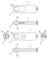
図1は、本発明の第1実施形態に係る撮影装置10の構成を示す六面図である。図2は、撮影装置10の内部構造を模式的に示す図である。[First embodiment]
Fig. 1 is a six-view diagram showing the configuration of an
撮影装置10は、2つの撮像系20A、20Bを備える。撮影装置10は、2つの撮像系20A、20Bにより撮像された像を合成して4πラジアンの立体角内の像(全天球画像)を生成する。撮影装置10は、この全天球画像を外部装置に出力する。出力先の外部装置は、例えばディスプレイ装置や印刷装置である。なお、撮影装置10は、全天球画像だけでなく、水平面のみ360度を撮影した、いわゆるパノラマ画像を生成することもできる。The image capturing
なお、本実施形態に係る撮影装置10は、電子機器の一例であるカメラであるが、スマートフォンやタブレット端末等の撮影機能を有する別の形態の電子機器であってもよい。すなわち、撮影装置10は、2つの撮像系20A、20Bを備え、2つの撮像系により撮像された像を合成して全天球画像を生成することが可能なスマートフォンやタブレット端末等であってもよい。The
撮像系20Aは、結像光学系22A及び撮像素子24Aを有する。撮像系20Bは、結像光学系22B及び撮像素子24Bを有する。撮像素子24A及び24Bは、例えばCMOS(Complementary Metal Oxide Semiconductor)やCCD(Charge-Coupled Device)イメージセンサである。The
図1に示されるように、撮影装置10は、筐体12を備える。本実施形態において、筐体12は、堅牢性や高級感を得るため、例えばマグネシウム合金等の金属製部材となっている。なお、筐体12は、金属粉を含有させた樹脂製部材(すなわち一部に金属を含む部材)であってもよい。このように、筐体12は、電磁的な遮蔽効果を有する部材で形成される。As shown in FIG. 1, the
筐体12は、撮影装置10の各部材を収容し保持する本体部と、この本体部を覆うカバー部(外装)を含む部材となっている。本実施形態では、本体部とカバー部は一体に形成されているが、別の実施形態では、本体部とカバー部は、別個の部品であってもよい。この場合、本体部とカバー部の少なくとも一方が、金属製部材又は一部に金属を含む部材、すなわち、電磁的な遮蔽効果を有する部材で形成される。The
筐体12には、バッテリ14、制御回路部16、鏡筒18A及び18Bが保持される。鏡筒18A及び18Bは、例えば樹脂製部材である。鏡筒18A及び18Bは、結像光学系22Aを保持するとともに結像光学系22Bを保持する。なお、鏡筒18Aと鏡筒18Bは、別部品であってもよく、また、一体に形成された部品であってもよい。The
結像光学系22A及び22Bは、それぞれ半球画像を結像するための、180度よりも大きい全画角を有する魚眼レンズであり、同一の光学特性を有する。図1及び図2に示されるように、結像光学系22Aは、撮影装置10の上部正面側に設けられ、結像光学系22Bは、撮影装置10の上部背面側に設けられる。結像光学系22Aが向く方向と結像光学系22Bが向く方向は180度異なる。The imaging
図3は、撮像系20A及び20Bを含む部分を拡大して示す図である。図3に示されるように、結像光学系22Aは、物体側から順に、第1レンズ群GA1、プリズムPA、第2レンズ群GA2を有する。プリズムPAと第2レンズ群GA2との間に開口絞りSAが配置される。第2レンズ群GA2の像側にフィルタFAが配置される。結像光学系22Bは、物体側から順に、第1レンズ群GB1、プリズムPB、第2レンズ群GB2を有する。プリズムPBと第2レンズ群GB2との間に開口絞りSBが配置される。第2レンズ群GB2の像側にフィルタFBが配置される。Figure 3 is an enlarged view of a portion including
筐体12の正面に開口部12Aが形成され、筐体12の背面に開口部12Bが形成される。開口部12Aには、鏡筒18A及び鏡筒18Bに保持された結像光学系22Aが開口部12Aを塞ぐように取り付けられる。開口部12Bには、鏡筒18A及び鏡筒18Bに保持された結像光学系22Bが開口部12Bを塞ぐように取り付けられる。An opening 12A is formed on the front side of the
結像光学系22A及び22Bは、全ての光学部材が光学ガラス材料によって形成されてもよく、また、全ての光学部材が樹脂材料によって形成されてもよい。また、結像光学系22A及び22Bは、一部の光学部材が光学ガラス材料によって形成され、残りの光学部材が樹脂材料によって形成されてもよい。All of the optical components of the imaging
プリズムPA、PBは、それぞれ、反射面RA、RBを有する直角プリズムであり、鏡筒18Aの端面18Aaと鏡筒18Bの端面18Baとの間に配置される。プリズムPAは、鏡筒18Aの端面18Aaに接着され、プリズムPBは、鏡筒18Bの端面18Baに接着されている。Prisms PA and PB are right-angle prisms having reflecting surfaces RA and RB, respectively, and are disposed between end face 18Aa of
プリズムPAは、反射面RAにより、第1レンズ群GA1からの光の光路を第2レンズ群GA2に向けて90度屈曲させる。すなわち、第1レンズ群GA1を通過した被写体光束は、反射面RAにて90度屈曲され、開口絞りSAを通過して第2レンズ群GA2に入射される。この被写体光束は、第2レンズ群GA2及びフィルタFAを通過して、撮像素子24Aの撮像面に入射される。撮像素子24Aは、この撮像面上にて受光した被写体の光学像を画像信号に変換して、制御回路部16に出力する。The prism PA bends the optical path of light from the first lens group GA1 by 90 degrees toward the second lens group GA2 with the reflecting surface RA. That is, the subject light flux that passes through the first lens group GA1 is bent by 90 degrees at the reflecting surface RA, passes through the aperture stop SA, and enters the second lens group GA2. This subject light flux passes through the second lens group GA2 and the filter FA, and is entered into the imaging surface of the
プリズムPBは、反射面RBにより、第1レンズ群GB1からの光の光路を第2レンズ群GB2に向けて90度屈曲させる。すなわち、第1レンズ群GB1を通過した被写体光束は、反射面RBにて90度屈曲され、開口絞りSBを通過して第2レンズ群GB2に入射される。この被写体光束は、第2レンズ群GB2及びフィルタFBを通過して、撮像素子24Bの撮像面に入射される。撮像素子24Bは、この撮像面上にて受光した被写体の光学像を画像信号に変換して、制御回路部16に出力する。The prism PB bends the optical path of light from the first lens group GB1 by 90 degrees toward the second lens group GB2 with the reflecting surface RB. That is, the subject light flux that passes through the first lens group GB1 is bent by 90 degrees at the reflecting surface RB, passes through the aperture stop SB, and enters the second lens group GB2. This subject light flux passes through the second lens group GB2 and the filter FB, and is entered into the imaging surface of the
制御回路部16は、撮影装置10を動作させるための各種回路(DSP(Digital Signal Processor)16a及びCPU(Central Processing Unit)16bを搭載したシステムLSI(Large-scale Integrated Circuit)、RAM(Random Access Memory)、ROM(Read Only Memory)等のメモリ、A/Dコンバータ等)を基板に実装したものである。制御回路部16において、ROMに格納されているプログラムがDSP16aやCPU16bで実行されることにより、撮影装置10が動作する。DSP16aは、撮像素子24A、24Bの各々より入力される画像信号を1つの画像に合成して全天球画像を生成して外部装置に出力する。The
このように、撮影装置10は、全画角が360度/nより大きい結像光学系を2つ有し(本実施形態では、nは2であり、全画角が180度よりも大きい結像光学系22A、22Bを有し)、結像光学系22A、22Bの各々による像を撮像する2つの撮像素子24A、24Bと、撮像素子24A、24Bの各々より入力される画像信号を1つの画像に合成して全天球画像を生成するDSP16a(画像生成部)を備える構成となっている。In this way, the photographing
制御回路部16の基板には、通信モジュール30が有する無線通信IC(Integrated Circuit)32も実装されている。通信モジュール30は、無線通信IC32に加えてアンテナ部材34を有する。The wireless communication IC (Integrated Circuit) 32 of the
通信モジュール30は、Bluetooth(登録商標)やWiFi等の短距離無線通信規格に準拠した無線通信モジュールである。DSP16aにより生成された全天球画像データは、通信モジュール30を介して、無線接続されたディスプレイ装置や印刷装置に伝送される。The
反射面RAの反対側の面であるプリズムPAの背面を「プリズム背面BA」と記し、反射面RBの反対側の面であるプリズムPBの背面を「プリズム背面BB」と記す。図3に示されるように、プリズムPAとプリズムPBは、プリズム背面BAとプリズム背面BBとが間隔を空け且つ互いに向き合うように配置される。プリズム背面BAとプリズム背面BBは平行である。The back surface of prism PA, which is the surface opposite reflecting surface RA, is referred to as "prism back surface BA," and the back surface of prism PB, which is the surface opposite reflecting surface RB, is referred to as "prism back surface BB." As shown in FIG. 3, prisms PA and PB are arranged such that prism back surface BA and prism back surface BB are spaced apart and face each other. Prism back surface BA and prism back surface BB are parallel.
また、図3に示されるように、開口部12Aの周縁部(すなわち開口部12Aの形状を規定する縁部の全周)を含む平面を「平面PLA」と記し、開口部12Bの周縁部(すなわち開口部12Bの形状を規定する縁部の全周)を含む平面を「平面PLB」と記す。Also, as shown in FIG. 3, the plane including the peripheral portion of
アンテナ部材34(より詳細には、後述するアンテナパターン34a)は、筐体12の内部であり且つ結像光学系22A及び22Bの光路外であって、図3に示されるように、開口部12A、12Bのそれぞれにおいて、平面PLA、PLBへの正射影OPA、OPBの少なくとも一部が、開口部12A、12Bの周縁部によって囲われる、平面PLA、PLB上の領域PAr、PBrに含まれるように位置している。The antenna member 34 (more specifically, the
すなわち、撮影装置10は、アンテナ部材34を、結像光学系22A及び22Bの光路外であって、開口部12A、12Bのそれぞれにおいて、平面PLA、PLBへの正射影OPA、OPBの少なくとも一部が平面PLA、PLB上の領域PAr、PBrに含まれるように配置するステップ、を含む方法によって製造されている。That is, the
「アンテナ部材34の正射影OPAの少なくとも一部が領域PArに含まれるように位置する」は、「開口部12Aを正面視したときに(且つ開口部12Aとアンテナ部材34間の部材が視覚的に透明であるものとすると)アンテナ部材34の少なくとも一部が視認できる位置にアンテナ部材34が配置される」と言い換えることができる。また、「アンテナ部材34の正射影OPBの少なくとも一部が領域PBrに含まれるように位置する」は、「開口部12Bを正面視したときに(且つ開口部12Bとアンテナ部材34間の部材が視覚的に透明であるものとすると)アンテナ部材34の少なくとも一部が視認できる位置にアンテナ部材34が配置される」と言い換えることができる。"Positioned so that at least a part of the orthogonal projection OPA of the
本実施形態では、アンテナ部材34は、互いに向き合って配置されたプリズム背面同士の隙間(プリズム背面BAとプリズム背面BBとの間)に配置されている。アンテナ部材34は、プリズム背面BAとプリズム背面BBの少なくとも一方に接着されている。In this embodiment, the
付言するに、アンテナ部材34は、図3に示されるように、第1レンズ群GA1の光軸AXAの延長線と交差する位置に配置され、且つ、第1レンズ群GB1の光軸AXBの延長線と交差する位置に配置されている。In addition, as shown in FIG. 3, the
本実施形態において、アンテナ部材34は、回路基板(例えばリジット基板、リジットFPC(Flexible Printed Circuits)又はFPC)にアンテナパターン(配線パターン)34aをプリントしたものとなっている。鏡筒18Aには、インサート成形により金属板等の導電性部材18a(図3の破線参照)が埋設されている。導電性部材18aの一端は、アンテナパターン34aの端部と半田付けやコネクタ等(以下「半田等」と記す。)により接続され、導電性部材18aの他端は、信号線40の一端と半田等により接続されている。信号線40の他端は、無線通信IC32と半田等により接続されている。すなわち、アンテナパターン34aは、導電性部材18a及び信号線40を介して無線通信IC32と電気的に接続される。In this embodiment, the
なお、導電性部材18aを省き、信号線40をアンテナパターン34aに直接接続する構成を採用してもよい。この場合、信号線40は、例えば、鏡筒18Aを筐体12に組み付ける工程中に筐体12と鏡筒18Aとの隙間を通されて、アンテナパターン34aに接続される。It is also possible to omit the
また、アンテナ部材34がFPCである場合、このFPCが無線通信IC32まで延びて無線通信IC32と直接接続される構成としてもよい。この場合、導電性部材18a及び信号線40に代えて、FPC上に形成された導体パターンが、アンテナパターン34aと無線通信IC32とを電気的に接続する。In addition, when the
本実施形態では、プリズム背面BAとプリズム背面BBの少なくとも一方にアンテナ部材34が接着されている。但し、プリズムによっては、背面が空気層でなければ(すなわち背面に部材が接触しない状態でなければ)、第1レンズ群GA1からの被写体光束を第2レンズ群GA2に向けて反射させる(より詳細には全反射させる)ことができない。この種のプリズムを用いる場合、例えば、支持体に取り付けられたアンテナ(例えば板金アンテナ)の先端をプリズム背面BAとプリズム背面BBとの間に挿入し、アンテナがプリズム背面BA及びプリズム背面BBと接触しないように、この支持体を鏡筒18Aや筐体12等に固定する構成が採用される。In this embodiment, the
正射影OPA、OPBの少なくとも一部が領域PAr、PBrに含まれるようにアンテナ部材34を配置することにより(別の観点では、アンテナ部材34が第1レンズ群GA1の光軸AXAの延長線と交差する位置に配置され、且つ、第1レンズ群GB1の光軸AXBの延長線と交差する位置に配置されることにより)、筐体12に形成された複数の開口部12A及び12Bがアンテナ部材34の周囲に位置することになる。By positioning the
開口部12Aは結像光学系22Aによって塞がれ、開口部12Bは結像光学系22Bによって塞がれているものの、金属製部材である筐体12によっては塞がれていない。結像光学系22A及び22Bは、光学ガラス部材や樹脂部材であるため、アンテナパターン34aより放射される電波を遮蔽したり大幅に減衰させたりすることがない。すなわち、アンテナパターン34aより放射される電波は、筐体12の金属部分によって遮蔽されたり減衰されたりすることなく、結像光学系22A及び22Bを通過して撮影装置10の外部に放射される。The
このように、本実施形態によれば、金属製の筐体12の一部を非金属製部材で形成しなくとも、アンテナパターン34aの放射特性の劣化が抑制される。これにより、筐体12の一部を非金属製部材で形成する必要があるために生じるデザイン上の制約がなくなり、また、筐体12の一部を非金属製部材で形成することによる筐体12の剛性の低下が避けられる。In this way, according to this embodiment, the deterioration of the radiation characteristics of the
アンテナ部材34による被写体光束のケラレを避けるため、アンテナ部材34を結像光学系22A及び22Bの光路外に配置する必要がある。結像光学系22A及び22Bの光路を避けてアンテナ部材34を配置する方法として、例えば筐体12を大きく形成して撮像系20A及び20Bの周囲(例えば撮像素子24Bの上方部分)にスペースを確保することが考えられる。To avoid vignetting of the subject light beam by the
しかし、この構成では、筐体12が大型化するだけでなく、正射影OPA、OPBの少なくとも一部が領域PAr、PBrに含まれるようにアンテナ部材34を配置すること(別の観点では、アンテナ部材34を、第1レンズ群GA1の光軸AXAの延長線と交差する位置に配置し、且つ、第1レンズ群GB1の光軸AXBの延長線と交差する位置に配置すること)が難しいため、アンテナパターン34aの放射特性の劣化の抑制することが難しい。However, with this configuration, not only does the
そこで、本実施形態では、アンテナ部材34は、プリズム背面BAとプリズム背面BBとの間に配置されている。これにより、筐体12に形成された複数の開口部12A及び12Bがアンテナ部材34の周囲に位置するとともに、アンテナ部材34を設置するためのスペースがプリズム背面同士の隙間だけであるため、筐体12を小型に設計しやすくなる。また、上記の構成と比べて、各開口部12A、12Bとアンテナ部材34との距離が短いため、各開口部12A、12Bより放射される電波の放射角が広くなる。なお、プリズム背面同士の隙間は、回路基板がFPCの場合、一例として0.2mmであり、回路基板がリジット基板の場合、一例として0.3mmである。Therefore, in this embodiment, the
また、アンテナ部材34をプリズム背面BAとプリズム背面BBとの間に配置したことにより、結像光学系22Aの最も物体側のレンズLAとアンテナ部材34との間、及び結像光学系22Bの最も物体側のレンズLBとアンテナ部材34との間に、金属部材が配置されないこととなる。そのため、アンテナパターン34aより放射された電波は、金属部材により遮蔽されたり大幅に減衰されたりすることなく、開口部12A及び12Bを介して撮影装置10の外部に放射される。In addition, by disposing the
アンテナ部材34近傍に金属があると、アンテナパターン34aより放射された電波がその金属によって遮蔽されたり減衰されたりするため、開口部12A及び12Bから電波を効率よく放射させることが難しい。電波の放射効率を向上させるため、本実施形態では、アンテナ部材34をプリズム背面BAとプリズム背面BBとの間に配置している。すなわち、本実施形態では、アンテナ部材34の周囲に、主に光学部材(具体的には、第1レンズ群GA1、GB1、プリズムPA、PB、第2レンズ群GA2及びGB2)が位置し、金属を含む部材が殆ど位置しない構成とすることにより、電波の放射効率を向上させている。If there is metal near the
[第2実施形態]
図4は、第2実施形態に係る撮影装置110の内部構造を模式的に示す図である。撮影装置110は、略球形状を有する撮影装置であり、筐体112、バッテリ114、制御回路部116、鏡筒118A、118B、撮像系120A、120B及び通信モジュール130を備える。撮像系120Aは、結像光学系122A及び撮像素子124Aを有する。撮像系120Bは、結像光学系122B及び撮像素子124Bを有する。通信モジュール130は、無線通信IC132及びアンテナ部材134を有する。[Second embodiment]
4 is a diagram showing a schematic internal structure of the
外形状が略球形状である筐体112に開口部112Aが形成され、略球形状の中心位置を挟んで開口部112Aの反対側に開口部112Bが形成される。開口部112Aには、鏡筒118Aに保持された結像光学系122Aが開口部112Aを塞ぐように取り付けられる。開口部112Bには、鏡筒118Bに保持された結像光学系122Bが開口部112Bを塞ぐように取り付けられる。An
本実施形態に係る結像光学系122A及び122Bは、途中で光路を屈曲させる屈曲光学系ではない。結像光学系122A、122Bは、それぞれ、第1実施形態に係る結像光学系22A、22BからプリズムPA、PB、開口絞りSA、SBを無くし且つ第1レンズ群及び第2レンズ群の光軸が一致する構成となっている。The imaging
撮像素子124Aの撮像面の反対側の面である撮像素子124Aの背面を「撮像素子背面BA’」と記し、撮像素子124Bの撮像面の反対側の面である撮像素子124Bの背面を「撮像素子背面BB’」と記す。図4に示されるように、撮像素子124Aと撮像素子124Bは、撮像素子背面BA’と撮像素子背面BB’とが間隔を空け且つ互いに向き合うように配置される。撮像素子背面BA’と撮像素子背面BB’は平行である。The rear surface of
アンテナ部材134は、筐体112の内部であり且つ結像光学系122A及び122Bの光路外であって、図4に示されるように、開口部112A、112Bのそれぞれにおいて、平面PLA、PLBへの正射影OPA、OPBの少なくとも一部が、開口部112A、112Bの周縁部によって囲われる、平面PLA、PLB上の領域PAr、PBrに含まれるように位置している。The
具体的には、本実施形態では、アンテナ部材134は、互いに向き合って配置された撮像素子背面同士の隙間(撮像素子背面BA’と撮像素子背面BB’との間)に配置されている。アンテナ部材134は、図4に示されるように、筐体112に形成された保持部112Cに保持されている。Specifically, in this embodiment, the
本実施形態においても、正射影OPA、OPBの少なくとも一部が領域PAr、PBrに含まれるようにアンテナ部材134を配置することにより、筐体112に形成された複数の開口部112A及び112Bがアンテナ部材134の周囲に位置することになる。開口部112Aは結像光学系122Aによって塞がれ、開口部112Bは結像光学系122Bによって塞がれているものの、金属製部材である筐体112によっては塞がれていない。結像光学系122A及び122Bは、光学ガラス部材や樹脂部材であるため、アンテナ部材134が有するアンテナパターン134aより放射される電波を遮蔽したり大幅に減衰させたりすることがない。すなわち、アンテナパターン134aより放射される電波は、筐体112の金属部分によって遮蔽されたり減衰されたりすることなく、結像光学系122A及び122Bを通過して撮影装置110の外部に放射される。In this embodiment, the
このように、本実施形態においても、金属製の筐体112の一部を非金属製部材で形成しなくとも、アンテナパターン134aの放射特性の劣化が抑制される。これにより、筐体112の一部を非金属製部材で形成する必要があるために生じるデザイン上の制約がなくなり、また、筐体112の一部を非金属製部材で形成することによる筐体112の剛性の低下が避けられる。In this manner, even in this embodiment, deterioration of the radiation characteristics of the
なお、アンテナパターン134aの全体が撮像素子背面BA’と撮像素子背面BB’との間に配置されてしまうと、撮像素子124A及び124Bによる電波の遮蔽及び減衰により、開口部112A及び112Bから電波を効率よく放射させることが難しい。そこで、本実施形態では、図4に示されるように、アンテナ部材134(アンテナパターン134a)の一部が撮像素子背面BA’と撮像素子背面BB’との隙間から出るように、アンテナ部材134を配置する。これにより、撮像素子124A及び124Bによる電波の遮蔽及び減衰を抑制し、電波の放射効率を向上させている。If the
本実施形態では、電波の放射効率の向上のため、例えば、撮像素子背面BA’と撮像素子背面BB’との間に配置されるアンテナパターン134aは、その全体のうちの1/3以下に抑えられる。また、アンテナ部材134は例えば厚みが0.2mmのFPCであり、撮像素子背面同士の隙間は、例えば1.2mm(撮像素子背面BA’とアンテナ部材134との隙間が0.5mmであり、撮像素子背面BB’とアンテナ部材134との隙間が0.5mm)である。アンテナ部材134と各撮像素子背面との隙間を0.5mmほど確保することにより、アンテナパターン134aが各撮像素子(金属板に相当する部材)と近接することによる容量結合によってアンテナパターン134aの放射特性が劣化するという問題が生じ難くなる。In this embodiment, in order to improve the efficiency of radio wave radiation, for example, the
以上が本発明の例示的な実施形態の説明である。本発明の実施形態は、上記に説明したものに限定されず、本発明の技術的思想の範囲において様々な変形が可能である。例えば明細書中に例示的に明示される実施形態等又は自明な実施形態等を適宜組み合わせた内容も本願の実施形態に含まれる。The above is an explanation of exemplary embodiments of the present invention. The embodiments of the present invention are not limited to those described above, and various modifications are possible within the scope of the technical concept of the present invention. For example, the embodiments of the present application also include appropriate combinations of embodiments explicitly shown as examples in the specification or obvious embodiments.
上記の実施形態において、アンテナ部材34は、回路基板にプリントされたアンテナパターン34aを有する構成であるが、本発明に係るアンテナ部材34は、この構成に限らない。アンテナ部材34は、回路基板にチップアンテナを実装した構成に置き換えてもよく、また、回路基板に板金アンテナを取り付けた構成に置き換えてもよく、また、樹脂製部品(例えばポリエチレンテレフタレート製のフィルムシート)にアンテナパターンをプリントした構成に置き換えてもよい。なお、これらの構成に置き換えた場合、プリズム背面同士の隙間として0.2mmより大きい隙間が必要となる。一例として、FPCにチップアンテナを実装した構成では、プリズム背面同士の隙間として0.8mmが必要となる。In the above embodiment, the
また、鏡筒18Aは、導電性部材18aの一部が鏡筒18Aの外部に突出した構成であってもよい。この場合、鏡筒18Aの外部に突出した導電性部材18aの一部をアンテナ部材34として形成してもよい。The
上記の実施形態において、無線通信IC32とアンテナパターン34aは、導電性部材18a及び信号線40を介して電気的に接続されるが、無線通信IC32とアンテナパターン34aとの接続方法はこれに限らない。例えば、無線通信IC32とアンテナ部材34のそれぞれに中継アンテナを設けた構成を採用してもよい。この場合、無線通信IC32とアンテナパターン34aは、中継アンテナを介して無線接続される。なお、中継アンテナ同士の通信には、混信を避けるため、外部通信用の周波数帯(BluetoothやWiFi等)とは異なる周波数帯が用いられる。In the above embodiment, the
上記の実施形態では、全画角が180度よりも大きい結像光学系を有する一対の撮像系(すなわち2つの撮像系)を備える撮影装置を示したが、本発明に係る撮影装置の構成はこれに限らない。全画角が360度/n(nは3以上の自然数)より大きい結像光学系と結像光学系による像を撮像する撮像素子とを有する撮像系をn個備え、n個の撮像系により撮像された像を合成して4πラジアンの立体角内の像を生成する電子機器も本発明の範疇である。In the above embodiment, a photographing device equipped with a pair of imaging systems (i.e., two imaging systems) having an imaging optical system with a total angle of view greater than 180 degrees was shown, but the configuration of the photographing device according to the present invention is not limited to this. The present invention also includes an electronic device that has n imaging systems each having an imaging optical system with a total angle of view greater than 360 degrees/n (n is a natural number of 3 or more) and an image sensor that captures an image by the imaging optical system, and that synthesizes the images captured by the n imaging systems to generate an image within a solid angle of 4π radians.
図5は、変形例に係る撮影装置210の概略構成を示す図である。本変形例に係る撮影装置210はペン型の撮影装置であり、全画角が90度より大きい結像光学系と結像光学系による像を撮像する撮像素子とを有する撮像系を4つ備え、4つの撮像系により撮像された像を合成して4πラジアンの立体角内の像を生成する。Figure 5 is a diagram showing the schematic configuration of an
撮影装置210は、筐体212の前後左右に開口部212A、212B、212C、212Dが形成されており、4つの撮像系の各々が撮影装置210の中心軸AX周りに90度ずつずらして配置されている。開口部212A、212B、212C、212Dには、それぞれ、結像光学系222A、222B、222C、222Dが取り付けられている。The
図5に示されるように、アンテナ部材234は、開口部212Aと開口部212Cとの中間位置で且つ開口部212Bと開口部212Dとの中間位置に配置されている。具体的には、アンテナ部材234は、開口部212A、212B、212C、212Dのそれぞれにおいて、平面PLA、PLB、PLC、PLDへの正射影OPA、OPB、OPC、OPDの少なくとも一部が、開口部212A、212B、212C、212Dの周縁部によって囲われる、平面PLA、PLB、PLC、PLD上の領域PAr、PBr、PCr、PDrに含まれるように位置している。なお、「平面PLC」は、開口部212Cの周縁部を含む平面であり、「平面PLD」は、開口部212Dの周縁部を含む平面である。また、図5では、便宜上、平面PLA、PLB、PLC、PLD、正射影OPA、OPB、OPC、OPD、領域PAr、PBr、PCr、PDrの図示を省略している。5, the
本変形例では、筐体212に形成された複数の開口部212A、212B、212C、212Dがアンテナ部材234の周囲に位置する。アンテナ部材234が有するアンテナパターン234aより放射される電波は、上記の実施形態と同様に、筐体212の金属部分によって遮蔽されたり減衰されたりすることなく、各結像光学系を通過して撮影装置210の外部に放射される。In this modified example,
本変形例では、アンテナ部材234の周囲に多数(具体的には4つ)の開口部が位置するため、アンテナパターン234aより放射される電波が全方位に放射されやすくなっている。In this modified example, multiple openings (specifically, four) are located around the
10 撮影装置
12 筐体
14 バッテリ
16 制御回路部
18A、18B 鏡筒
20A、20B 撮像系
22A、22B 結像光学系
24A、24B 撮像素子
34 アンテナ部材
34a アンテナパターンREFERENCE SIGNS LIST 10: IMAGING APPARATUS 12: HOUSING 14: BATTERY 16:
Claims (9)
Translated fromJapanese前記複数の開口部のそれぞれに、前記開口部を塞ぐように取り付けられた複数の結像光学系と、
前記筐体の内部に設けられたアンテナ部材と、
を備え、
前記アンテナ部材は、
前記複数の結像光学系の光路外であって、前記複数の開口部のそれぞれにおいて、前記開口部の周縁部を含む平面への正射影の少なくとも一部が、前記周縁部によって囲われる前記平面上の領域に含まれるように位置している、
電子機器。 A housing having a plurality of openings;
a plurality of imaging optical systems attached to the plurality of openings so as to cover the respective openings;
An antenna member provided inside the housing;
Equipped with
The antenna member includes:
a projection lens that projects from the aperture onto a plane including a periphery of the aperture, the projection lens being positioned outside the optical path of the plurality of imaging optical systems, such that at least a part of an orthogonal projection of the aperture onto a plane including a periphery of the aperture is included in an area on the plane surrounded by the periphery;
Electronics.
前記複数の結像光学系の各々の光軸の延長線と交差する位置に配置されている、
請求項1に記載の電子機器。 The antenna member includes:
Located at a position intersecting an extension line of the optical axis of each of the plurality of imaging optical systems,
2. The electronic device according to claim 1.
物体側から順に、第1レンズ群、プリズム、第2レンズ群を有し、
前記プリズムは、
反射面を有し、
前記反射面により、前記第1レンズ群からの光の光路を前記第2レンズ群に向けて屈曲させ、
前記複数の結像光学系の各々が有するプリズムは、
前記反射面の反対側の面であるプリズム背面が間隔を空け且つ互いに向き合うように配置され、
前記アンテナ部材は、
互いに向き合って配置された前記プリズム背面同士の隙間に配置されている、
請求項1又は請求項2に記載の電子機器。 The imaging optical system includes:
The optical system has, in order from the object side, a first lens group, a prism, and a second lens group,
The prism is
A reflecting surface is provided.
the optical path of the light from the first lens group is bent toward the second lens group by the reflecting surface;
The prism included in each of the plurality of imaging optical systems is
The prism rear surfaces, which are the surfaces opposite to the reflecting surfaces, are arranged to face each other with a gap therebetween,
The antenna member includes:
The prism rear surfaces are disposed in a gap between the prism rear surfaces that are disposed facing each other.
3. The electronic device according to claim 1 or 2.
請求項1から請求項3の何れか一項に記載の電子機器。 No metal member is disposed between the lens closest to the object side of the imaging optical system and the antenna member.
The electronic device according to claim 1 .
を更に備え、
前記複数の撮像素子は、
前記撮像面の反対側の面である撮像素子背面が間隔を空け且つ互いに向き合うように配置され、
前記アンテナ部材は、
互いに向き合って配置された前記撮像素子背面同士の隙間に配置されている、
請求項1又は請求項2に記載の電子機器。 a plurality of image pickup elements that receive light that has passed through each of the plurality of imaging optical systems at an image pickup surface and convert the light into an image signal;
The plurality of image pickup elements include
The rear surfaces of the imaging elements, which are surfaces opposite to the imaging surfaces, are disposed so as to face each other with a gap therebetween,
The antenna member includes:
The imaging element is disposed in a gap between the rear surfaces of the imaging elements that are disposed facing each other.
3. The electronic device according to claim 1 or 2.
金属製部材又は一部に金属を含む部材である、
請求項1から請求項5の何れか一項に記載の電子機器。 The housing includes:
The member is made of metal or contains metal in part.
The electronic device according to claim 1 .
回路基板にアンテナパターンをプリントしたものである、
請求項1から請求項6の何れか一項に記載の電子機器。 The antenna member includes:
The antenna pattern is printed on a circuit board.
The electronic device according to any one of claims 1 to 6.
前記電子機器は、
前記n個の結像光学系の各々による像を撮像するn個の撮像素子と、
前記n個の撮像素子の各々より入力される画像信号を1つの画像に合成して全天球画像を生成する画像生成部と、
を更に備える、
請求項1から請求項7の何れか一項に記載の電子機器。 The imaging optical system includes n units of the imaging optical system, each of which has a total angle of view greater than 360 degrees/n (n is a natural number equal to or greater than 2);
The electronic device includes:
n image pickup elements for capturing images by the n image forming optical systems;
an image generating unit that generates a celestial sphere image by synthesizing image signals input from the n image pickup elements into one image;
Further comprising:
The electronic device according to claim 1 .
前記アンテナ部材を、前記複数の結像光学系の光路外であって、前記複数の開口部のそれぞれにおいて、前記開口部の周縁部を含む平面への正射影の少なくとも一部が、前記周縁部によって囲われる前記平面上の領域に含まれるように配置するステップ
を含む、
電子機器の製造方法。 A method for manufacturing an electronic device comprising: a housing having a plurality of openings; a plurality of imaging optical systems attached to the plurality of openings so as to cover the respective openings; and an antenna member provided inside the housing,
a step of disposing the antenna member outside the optical paths of the plurality of imaging optical systems, such that, in each of the plurality of openings, at least a part of an orthogonal projection onto a plane including a periphery of the opening is included in an area on the plane surrounded by the periphery,
Manufacturing method of electronic devices.
Priority Applications (1)
| Application Number | Priority Date | Filing Date | Title |
|---|---|---|---|
| JP2020095758AJP7484433B2 (en) | 2020-06-01 | 2020-06-01 | Electronic device and method for manufacturing electronic device |
Applications Claiming Priority (1)
| Application Number | Priority Date | Filing Date | Title |
|---|---|---|---|
| JP2020095758AJP7484433B2 (en) | 2020-06-01 | 2020-06-01 | Electronic device and method for manufacturing electronic device |
Publications (2)
| Publication Number | Publication Date |
|---|---|
| JP2021190903A JP2021190903A (en) | 2021-12-13 |
| JP7484433B2true JP7484433B2 (en) | 2024-05-16 |
Family
ID=78847628
Family Applications (1)
| Application Number | Title | Priority Date | Filing Date |
|---|---|---|---|
| JP2020095758AActiveJP7484433B2 (en) | 2020-06-01 | 2020-06-01 | Electronic device and method for manufacturing electronic device |
Country Status (1)
| Country | Link |
|---|---|
| JP (1) | JP7484433B2 (en) |
Citations (4)
| Publication number | Priority date | Publication date | Assignee | Title |
|---|---|---|---|---|
| JP2000075381A (en) | 1998-09-02 | 2000-03-14 | Olympus Optical Co Ltd | Camera incorporating position detection device |
| JP2007236700A (en) | 2006-03-09 | 2007-09-20 | Fujifilm Corp | Capsule endoscope system |
| JP2014030104A (en) | 2012-07-31 | 2014-02-13 | Ricoh Co Ltd | Receiving device, image sharing system, receiving method, and program |
| JP2020005246A (en) | 2018-06-26 | 2020-01-09 | 株式会社リコー | Imaging apparatus |
Family Cites Families (1)
| Publication number | Priority date | Publication date | Assignee | Title |
|---|---|---|---|---|
| US20160058272A1 (en)* | 2014-08-28 | 2016-03-03 | Panasonic Intellectual Property Management Co., Ltd. | Capsule endoscope, capsule endoscope system, and method for controlling posture of capsule endoscope |
- 2020
- 2020-06-01JPJP2020095758Apatent/JP7484433B2/enactiveActive
Patent Citations (4)
| Publication number | Priority date | Publication date | Assignee | Title |
|---|---|---|---|---|
| JP2000075381A (en) | 1998-09-02 | 2000-03-14 | Olympus Optical Co Ltd | Camera incorporating position detection device |
| JP2007236700A (en) | 2006-03-09 | 2007-09-20 | Fujifilm Corp | Capsule endoscope system |
| JP2014030104A (en) | 2012-07-31 | 2014-02-13 | Ricoh Co Ltd | Receiving device, image sharing system, receiving method, and program |
| JP2020005246A (en) | 2018-06-26 | 2020-01-09 | 株式会社リコー | Imaging apparatus |
Also Published As
| Publication number | Publication date |
|---|---|
| JP2021190903A (en) | 2021-12-13 |
Similar Documents
| Publication | Publication Date | Title |
|---|---|---|
| US7802996B2 (en) | Image pickup apparatus | |
| CN111566556B (en) | camera | |
| EP4376566A1 (en) | Camera module for heat dissipation and grounding, and electronic device comprising same | |
| KR20070047721A (en) | Image pickup device mounting structure | |
| JP5387046B2 (en) | The camera module | |
| EP4181499A1 (en) | Electronic device comprising camera module | |
| EP4096372A1 (en) | Electronic device comprising interposer | |
| WO2007125761A1 (en) | Compound eye camera module | |
| EP4138533B1 (en) | Electronic device including shield can | |
| CN217825080U (en) | Camera module, camera device and electronic equipment | |
| TWI877467B (en) | Lens assembly device | |
| JP7484433B2 (en) | Electronic device and method for manufacturing electronic device | |
| CN216217096U (en) | Camera module and electronic equipment | |
| JP7551355B2 (en) | Accessory shoe device, electronic device, shoe device and accessory device | |
| KR102842200B1 (en) | Camera module and electronic device including the same | |
| JP4787719B2 (en) | Imaging device | |
| JP2002171429A (en) | Compound eye imaging system, imaging device, and electronic device | |
| KR101859380B1 (en) | Multi-camera device | |
| KR102665774B1 (en) | Electronic device including shield can structure | |
| JP2021158555A (en) | Imaging apparatus | |
| KR102823728B1 (en) | Electronic device including interposer | |
| US12177546B2 (en) | Camera module and electronic device including the same | |
| JP7467958B2 (en) | Imaging device | |
| US20240405405A1 (en) | Imaging apparatus | |
| CN111565269B (en) | Image pickup apparatus |
Legal Events
| Date | Code | Title | Description |
|---|---|---|---|
| RD02 | Notification of acceptance of power of attorney | Free format text:JAPANESE INTERMEDIATE CODE: A7422 Effective date:20201007 | |
| A621 | Written request for application examination | Free format text:JAPANESE INTERMEDIATE CODE: A621 Effective date:20230412 | |
| RD03 | Notification of appointment of power of attorney | Free format text:JAPANESE INTERMEDIATE CODE: A7423 Effective date:20231025 | |
| A977 | Report on retrieval | Free format text:JAPANESE INTERMEDIATE CODE: A971007 Effective date:20240327 | |
| TRDD | Decision of grant or rejection written | ||
| A01 | Written decision to grant a patent or to grant a registration (utility model) | Free format text:JAPANESE INTERMEDIATE CODE: A01 Effective date:20240402 | |
| A61 | First payment of annual fees (during grant procedure) | Free format text:JAPANESE INTERMEDIATE CODE: A61 Effective date:20240415 | |
| R150 | Certificate of patent or registration of utility model | Ref document number:7484433 Country of ref document:JP Free format text:JAPANESE INTERMEDIATE CODE: R150 |