JP7479236B2 - Substrate Processing Equipment - Google Patents
Substrate Processing EquipmentDownload PDFInfo
- Publication number
- JP7479236B2 JP7479236B2JP2020130998AJP2020130998AJP7479236B2JP 7479236 B2JP7479236 B2JP 7479236B2JP 2020130998 AJP2020130998 AJP 2020130998AJP 2020130998 AJP2020130998 AJP 2020130998AJP 7479236 B2JP7479236 B2JP 7479236B2
- Authority
- JP
- Japan
- Prior art keywords
- region
- baffle plate
- shutter
- regions
- holes
- Prior art date
- Legal status (The legal status is an assumption and is not a legal conclusion. Google has not performed a legal analysis and makes no representation as to the accuracy of the status listed.)
- Active
Links
Images


Classifications
- H—ELECTRICITY
- H01—ELECTRIC ELEMENTS
- H01L—SEMICONDUCTOR DEVICES NOT COVERED BY CLASS H10
- H01L21/00—Processes or apparatus adapted for the manufacture or treatment of semiconductor or solid state devices or of parts thereof
- H01L21/67—Apparatus specially adapted for handling semiconductor or electric solid state devices during manufacture or treatment thereof; Apparatus specially adapted for handling wafers during manufacture or treatment of semiconductor or electric solid state devices or components ; Apparatus not specifically provided for elsewhere
- H01L21/67005—Apparatus not specifically provided for elsewhere
- H01L21/67011—Apparatus for manufacture or treatment
- H01L21/67017—Apparatus for fluid treatment
- H01L21/67063—Apparatus for fluid treatment for etching
- H01L21/67069—Apparatus for fluid treatment for etching for drying etching
- H—ELECTRICITY
- H01—ELECTRIC ELEMENTS
- H01J—ELECTRIC DISCHARGE TUBES OR DISCHARGE LAMPS
- H01J37/00—Discharge tubes with provision for introducing objects or material to be exposed to the discharge, e.g. for the purpose of examination or processing thereof
- H01J37/32—Gas-filled discharge tubes
- H01J37/32431—Constructional details of the reactor
- H01J37/32623—Mechanical discharge control means
- H01J37/32633—Baffles
- H—ELECTRICITY
- H01—ELECTRIC ELEMENTS
- H01J—ELECTRIC DISCHARGE TUBES OR DISCHARGE LAMPS
- H01J37/00—Discharge tubes with provision for introducing objects or material to be exposed to the discharge, e.g. for the purpose of examination or processing thereof
- H01J37/32—Gas-filled discharge tubes
- H01J37/32431—Constructional details of the reactor
- H01J37/32798—Further details of plasma apparatus not provided for in groups H01J37/3244 - H01J37/32788; special provisions for cleaning or maintenance of the apparatus
- H01J37/32816—Pressure
- H01J37/32834—Exhausting
- H—ELECTRICITY
- H01—ELECTRIC ELEMENTS
- H01L—SEMICONDUCTOR DEVICES NOT COVERED BY CLASS H10
- H01L21/00—Processes or apparatus adapted for the manufacture or treatment of semiconductor or solid state devices or of parts thereof
- H01L21/67—Apparatus specially adapted for handling semiconductor or electric solid state devices during manufacture or treatment thereof; Apparatus specially adapted for handling wafers during manufacture or treatment of semiconductor or electric solid state devices or components ; Apparatus not specifically provided for elsewhere
- H01L21/67005—Apparatus not specifically provided for elsewhere
- H01L21/67011—Apparatus for manufacture or treatment
- H01L21/67126—Apparatus for sealing, encapsulating, glassing, decapsulating or the like
Landscapes
- Engineering & Computer Science (AREA)
- Physics & Mathematics (AREA)
- Microelectronics & Electronic Packaging (AREA)
- General Physics & Mathematics (AREA)
- Manufacturing & Machinery (AREA)
- Computer Hardware Design (AREA)
- Condensed Matter Physics & Semiconductors (AREA)
- Power Engineering (AREA)
- Plasma & Fusion (AREA)
- Chemical & Material Sciences (AREA)
- Analytical Chemistry (AREA)
- Drying Of Semiconductors (AREA)
- Plasma Technology (AREA)
- Chemical Vapour Deposition (AREA)
Description
Translated fromJapanese本開示は、基板処理装置に関する。This disclosure relates to a substrate processing apparatus.
プラズマ処理装置の処理容器の側壁と載置台との間には、複数の穴を有する環状のバッフル板が設けられている。例えば、特許文献1は、アルミニウムで形成されたバッフル板の母材の表面にアルマイト層を形成し、アルマイト層を介してイットリアの膜を溶射し、これにより、プラズマに晒されるバッフル板の耐電圧を改善することを提案している。A ring-shaped baffle plate with multiple holes is provided between the side wall of the processing vessel of the plasma processing apparatus and the mounting table. For example,
本開示は、インピーダンス及びガスのコンダクタンスを調整することができる技術を提供する。This disclosure provides technology that can adjust impedance and gas conductance.
本開示の一の態様によれば、処理容器と、高周波電流を供給する高周波電源と、前記処理容器に電気的に接続された部材と、を有し、前記部材は、前記処理容器内の複数の特定の構成に対応する前記部材の複数の領域のそれぞれの単位体積あたりの表面積と、前記部材の複数の領域以外の領域である前記部材の第1の領域の単位体積あたりの表面積とが異なるように構成し、前記複数の特定の構成は、シャッター及び排気口を含み、前記部材の複数の領域は、前記シャッターに対応する第2の領域と、前記排気口に対応する第3の領域と、を有し、前記部材の複数の領域の各領域及び前記第1の領域は、領域毎に穴を有し、前記部材の複数の領域と前記第1の領域とは、前記穴の開口率が異なり、前記第2の領域に形成された穴は、前記第1の領域に形成された穴と形状及び/又は数が異なり、前記第3の領域に形成された穴は、前記第1の領域に形成された穴と形状及び/又は数が異なり、前記第2の領域に形成された穴と形状及び/又は数が異なる又は同じである、基板処理装置が提供される。 According to one aspect of the present disclosure, there is provided a substrate processing apparatus comprising: a processing vessel; a high-frequency power supply that supplies a high-frequency current; and a member electrically connected to the processing vessel, wherein the member is configured such that a surface area per unit volume of each of a plurality of regions ofthe member corresponding to a plurality of specific configurations in the processing vessel is different from a surface area per unit volume of a first region of the member that is a region other than the plurality of regions of the member, the plurality of specific configurations including a shutter and an exhaust port, the plurality of regions of the member having a second region corresponding to the shutter and a third region corresponding to the exhaust port, each of the plurality of regions of the member and the first region having a hole for each region, the plurality of regions of the member andthe first region having a different aperture ratio of the holes, the holes formed in the second region having a different shape and/or number than the holes formed in the first region, the holes formed in the third region having a different shape and/or number than the holes formed in the first region, and the holes formed in the third region having a different shape and/or number than or the same as the holes formed in the second region.
一の側面によれば、インピーダンス及びガスのコンダクタンスを調整することができる。According to one aspect, the impedance and gas conductance can be adjusted.
以下、図面を参照して本開示を実施するための形態について説明する。各図面において、同一構成部分には同一符号を付し、重複した説明を省略する場合がある。Below, a description will be given of a mode for carrying out the present disclosure with reference to the drawings. In each drawing, the same components are given the same reference numerals, and duplicate descriptions may be omitted.
[基板処理装置の全体構成]
まず、一実施形態に係る基板処理装置1の構成について、図1を参照して説明する。図1は、一実施形態に係る基板処理装置1の一例を示す断面模式図である。なお、本実施形態では、RIE(Reactive Ion Etching)型の基板処理装置1を例に挙げて説明する。 [Overall configuration of substrate processing apparatus]
First, the configuration of a
基板処理装置1は、金属製、例えば、アルミニウム又はステンレス鋼製の処理容器10を有し、その内部は、プラズマエッチングやプラズマCVD等のプラズマ処理が行われる処理空間Uとなっている。処理容器10は接地されている。処理容器10は、軸Axを中心軸とする円筒型の容器である。The
処理容器10の内部には、基板Wを載置する円板状のステージ11が配設されている。ステージ11は、基材11aと静電チャック25とを有する。基材11aは、例えば、アルミニウムからなり、絶縁性の筒状保持部材12を介して処理容器10の底から垂直上方に延びる筒状支持部13に支持されている。A disk-
静電チャック25は、基材11aの上に配置される。静電チャック25は、基板Wが載置される円板状の中央部25aと、中央部25aの外側の環状の周縁部25bとからなる。中央部25aの高さは周縁部25bの高さよりも高くなっている。処理容器10及びステージ11は、軸Axを共通にするように配置される。The
中央部25aは、導電膜からなる電極25cを有する。電極25cには直流電源26がスイッチ27を介して電気的に接続されている。静電チャック25は、直流電源26から電極25cに印加された直流電圧により静電力を発生させ、その静電力により基板Wを吸着保持する。周縁部25bの上面には、基板の周囲を環状に囲むエッジリング30(フォーカスリングともいう。)が載置されている。エッジリング30は、例えばシリコンから形成されている。The
ステージ11の内部には、例えば、円周方向に延在する環状の冷媒室31が設けられている。冷媒室31には、チラーユニット32から配管33、34を介して所定温度の熱媒体、例えば、冷却水が循環供給され、熱媒体の温度によって静電チャック25上の基板Wの温度を制御する。Inside the
静電チャック25には、ガス供給ライン36を介して伝熱ガス供給部35が接続されている。伝熱ガス供給部35は、ガス供給ライン36を用いて、静電チャック25の中央部25aの上面と、基板Wの下面とで挟まれる空間に伝熱ガスを供給する。伝熱ガスとしては、熱伝導性を有するガス、例えば、Heガス等が好適に用いられる。The
ステージ11には、プラズマ生成用およびRIE用の第1高周波電源21が整合器21aを介して電気的に接続されている。第1高周波電源21は、第1の高周波、例えば、40MHzの周波数の電力をステージ11に印加する。A first high
ステージ11には、イオン引き込み用の第2高周波電源22が整合器22aを介して電気的に接続されている。第2高周波電源22は、第1高周波よりも低い第2高周波、例えば、3MHzの周波数の電力をステージ11に印加する。A second high
また、処理容器10の天井部には、ガスシャワーヘッド24が配設されている。処理容器10及びガスシャワーヘッド24は、軸Axを共通にするように配置される。第1の高周波の電力及び/又は第2の高周波の電力が供給されることにより、ガスシャワーヘッド24(上部電極)とステージ11(下部電極)との間で高周波電界が生成される。処理ガス供給部40から出力された所定のガスは、ガスシャワーヘッド24からシャワー状に供給され、処理空間Uにて高周波電界によりプラズマ化する。A
処理容器10の内壁には、デポシールド52が着脱自在に設けられている。デポシールド52は、プラズマ処理中に生成される反応生成物が処理容器10の内壁に付着することを防止する。デポシールド52は、処理容器10の内壁及びステージ11の外周に設けられてもよい。A
処理容器10の内壁とステージ11との間には、排気路14が形成されている。排気路14の上方であって基板Wの下方の位置には、コニカル形状(円錐台形状)のバッフル板15が設けられている。バッフル板15は、ステージ11の外周に配置された部材53に固定されている。バッフル板15は、ガスの流れを整えるとともに、排気路14の空間にプラズマが侵入することを抑制する。処理容器10とバッフル板15は、軸Axを共通にするように配置される。An
処理空間Uの搬送口19に対応する部分は、シャッター51により開閉可能となっている。シャッター51は、シャッター51に接続されたリフター50の駆動により昇降し、処理容器10に設けられた搬送口19(開口)を開閉する。リフター50の駆動によりシャッター51が下降すると搬送口19が開き、シャッター51が上昇すると搬送口19が閉じる。The portion of the processing space U that corresponds to the
排気路14の底部には排気口16が形成されている。排気口16には、排気管17を介して排気装置18が接続されている。排気装置18は、真空ポンプを有し、処理容器10内の処理空間を所定の真空度まで減圧する。また、排気管17は可変式バタフライバルブである自動圧力制御弁(automatic pressure control valve)(以下、「APC」という)を有し(図示せず)、APCは自動的に処理容器10内の圧力制御を行う。さらに、処理容器10の側壁には、基板Wの搬送口19を開閉するゲートバルブ20が取り付けられている。An
排気口16は、処理容器10の底部であって処理容器10の上部から視認した場合にシャッター51の下方の左寄りの位置に偏在する。ただし、排気口16は、シャッター51の下方以外の位置で排気路14に連通してもよい。The
ガスシャワーヘッド24は、絶縁部材44を介して処理容器10の天井部に支持されている。ガスシャワーヘッド24は、電極板37と、電極板37を着脱可能に支持する電極支持体38とを有する。電極板37は、多数のガス通気孔37aを有する。電極支持体38の内部にはバッファ室39が設けられている。処理ガス供給部40は、ガス供給配管41を介してガス導入口38aに接続されている。処理ガス供給部40から供給されたガスは、バッファ室39に通され、多数のガス通気孔37aから処理容器10内に供給される。The
基板処理装置1の各構成要素は、制御部43に接続されている。制御部43は、基板処理装置1の各構成要素を制御する。各構成要素としては、例えば、排気装置18、第1高周波電源21、第2高周波電源22、スイッチ27、直流電源26、チラーユニット32、伝熱ガス供給部35および処理ガス供給部40が挙げられる。Each component of the
制御部43は、CPU43a及びメモリ43b(記憶装置)を備え、メモリ43bに記憶されたプログラム及び処理レシピを読み出して実行することで、基板処理装置1においてプラズマ処理を制御する。また、制御部43は、プラズマ処理に応じて、シャッター51の開閉処理、エッジリング30を静電吸着するための静電吸着処理及び伝熱ガスを供給する伝熱ガス供給処理等を制御する。The
処理容器10の周囲には、環状又は同心状に延びる磁石42が配置されている。基板処理装置1の処理容器10内では、磁石42によって一方向に向かう水平磁界が形成される。また、ステージ11とガスシャワーヘッド24との間に印加された高周波電力によって鉛直方向のRF電界が形成される。これにより、処理容器10内において処理ガスを介したマグネトロン放電が行われ、ステージ11の表面近傍において処理ガスから高密度のプラズマが生成される。A ring-shaped or
プラズマ処理において、基板処理装置1は、まず、ゲートバルブ20を開状態にして基板Wを搬送口19から搬入し、ステージ11上に載置する。排気装置18は処理容器10内を排気する。処理ガス供給部40は処理ガスを処理容器10内に導入する。伝熱ガス供給部35は、伝熱ガスを基板Wの裏面に供給する。第1高周波電源21がプラズマ生成用の高周波電力をステージ11に印加すると、処理ガスがプラズマ化し、プラズマ中のラジカルやイオンによって基板Wの表面に所定のプラズマ処理が行われる。第2高周波電源22からイオン引き込み用の高周波電力をステージ11に印加してもよい。In plasma processing, the
[バッフル板及びシャッターの構成]
次に、バッフル板15、シャッター51及びその周囲の構成について、図1及び図2を参照しながら説明する。図2は、一実施形態に係るバッフル板15、シャッター51及びその周囲の一例を示す拡大図である。 [Configuration of the baffle plate and shutter]
Next, the configuration of the
図1を参照すると、デポシールド52とステージ11との間にバッフル板15が設けられている。バッフル板15の上部の開口は、下部の開口よりも大きく、コニカル形状を有する。バッフル板15の上端の外側には、円周方向の一部の、搬送口19に対応する位置にシャッター51が昇降可能に設けられている。シャッター51が上昇すると、デポシールド52に当接し、これにより、搬送口19が閉じられる。バッフル板15の下端の内側には、ステージ11の外周に配置された部材53が設けられている。バッフル板15は、部材53を介して処理容器10の底部に固定されている。図2に拡大して示すように、バッフル板15の上端は環状のコンタクト部材54に接合されている。コンタクト部材54は、金属又は金属にセラミックスを被覆した構成である。Referring to FIG. 1, a
バッフル板15、シャッター51、デポシールド52及び部材53は、アルミニウム等の金属から形成されている。バッフル板15、シャッター51、デポシールド52及び部材53は、アルミニウム材に、アルミナ、イットリア(Y2O3)等のセラミックスを被覆したものを用いてもよい。 The
処理空間U(図1参照)の一部は、シャッター51により開閉可能となっている。基板Wの搬入及び搬出時、図2(a)に示すように、シャッター51に接続されたリフター50の駆動によりシャッター51を下降させてシャッター51を開ける。この状態でゲートバルブ20を開き、図示しない搬送アームを搬送口19から処理容器10内に差し入れ、基板Wを搬入又は搬出する。A portion of the processing space U (see FIG. 1) can be opened and closed by a
プラズマ処理中、図2(b)に示すように、リフター50の駆動によりシャッター51をデポシールド52及びコンタクト部材54に当接するまで上昇させ、シャッター51を閉じる。During plasma processing, as shown in FIG. 2(b), the
図2(b)に示すように、シャッター51を閉じると、シャッター51は、バッフル板15及びデポシールド52と接続され、バッフル板15及びデポシールド52は、グランド(処理容器10)へと高周波電流を流す経路となる。かかる構成により、処理空間Uには、高周波電力によりガスからプラズマが生成される。As shown in FIG. 2B, when the
処理容器10の底部に設けられた排気口16は、処理容器10の上部から視認した場合にシャッター51の下方の左寄りに偏って配置される(図5参照)。このため、排気口16の位置によって、バッフル板15の穴を通って排気口16から排気されるガスのコンダクタンスに偏りが生じる。また、シャッター51とデポシールド52の接触部分、及び、シャッター51とコンタクト部材54の接触部分は、インピーダンスの変化点となり高周波電流の流れが悪くなる。The
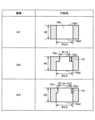
図3のバッフル板15の斜視図に示すように、シャッター51にオーバーラップするバッフル板15の領域Ar2及び領域Ar2の左側に隣接し、排気口16に対応する領域Ar3は、インピーダンス及び/又はガスのコンダクタンスの状態が領域Ar1と異なる。例えば、シャッター51とコンタクト部材54の接触部分は、インピーダンスの変化点となり高周波電流の流れが悪くなるため、領域Ar2は、領域Ar1よりもインピーダンスが高くなる。また、領域Ar3は、下方に排気口16があるため、領域Ar1よりもガスのコンダクタンスがよくなる。As shown in the perspective view of the
そこで、本実施形態に係るバッフル板15は、各領域のインピーダンス及びガスのコンダクタンスを調整するために、バッフル板15の領域Ar2及び領域Ar3と、領域Ar1との上面において穴の開口率を変える。例えば、バッフル板15は高周波電流が流れる経路となり、シャッター51が重なる部分にてコンタクト部材54の接触部分等により高周波電流の流れが悪くなる。そこで、領域Ar2の穴の上面(プラズマ側の面)の開口率を領域Ar1の穴の上面の開口率よりも小さくする。これにより、領域Ar2の上面の単位体積当たりの面積を領域Ar1の上面の単位体積当たりの面積よりも大きくすることでインピーダンスを調整し、バッフル板15の領域Ar2と領域Ar1とで高周波電流の流れ易さが同じになるように制御できる。Therefore, in the
また、例えば、排気口16に対応するバッフル板15の領域Ar3では、領域Ar1よりもガスの流れが良くなる。そこで、領域Ar3の穴の上面の開口率を領域Ar1の穴の上面の開口率よりも小さくする。これにより、領域Ar3と領域Ar1のガスの流れ易さが同じになる。これにより、バッフル板15の領域Ar3と領域Ar1とでガスのコンダクタンスが同じになるように制御できる。領域Ar2の穴の上面の開口率と領域Ar3の穴の上面の開口率は、インピーダンスの調整及びガスのコンダクタンスの調整ができれば、同じであってもよいし、異なってもよい。つまり、本実施形態では、バッフル板15は、処理容器10内の複数の特定の構成に対応するバッフル板15の領域Ar2及び領域Ar3のそれぞれの単位体積あたりの表面積が、領域Ar1の単位体積あたりの表面積と異なる。これにより、本実施形態に係るバッフル板15によれば、インピーダンスとガスのコンダクタンスを調整することができる。In addition, for example, the gas flow is better in the region Ar3 of the
なお、シャッター51及び排気口16は、処理容器10内の複数の特定の構成の一例である。ただし、処理容器10内の複数の特定の構成は、これらに限られず、シャッター51、排気口16、搬送口19、ゲートバルブ20、排気路14、排気管17、その他の処理容器10内の構成(部品、部分)の少なくとも2つであればよい。The
なお、バッフル板15及びデポシールド52は、処理容器に電気的に接続された部材の一例である。図3は、一実施形態に係るバッフル板15の一例を示す斜視図である。図3に示すように、本例では、バッフル板15の領域Ar3は、領域Ar2に隣接し、排気口16の位置に対応するが(図5参照)、領域Ar3は領域Ar2に隣接した領域に限られない。例えば、排気口16がシャッター51の位置と離れている場合、領域Ar3は領域Ar2に隣接しない場合がある。このように処理容器10内の特定の構成に応じてバッフル板15の領域Ar2、領域Ar3が定められる。また、バッフル板15は、処理容器10内の特定の構成に応じて領域Ar2、領域Ar3以外の1又は2以上の領域を有してもよい。例えば、図3において破線で示す領域Ar4のように、シャッター51に応じた領域Ar2、排気口16に応じた領域Ar3以外に処理容器10内の特定の構成に応じたバッフル板15の領域を有してもよい。特定の構成に応じたバッフル板15の領域Ar2、領域Ar3・・・以外のバッフル板15の領域が領域Ar1となる。The
領域Ar2、領域Ar3の単位体積あたりの表面積は、特定の構成に対応するバッフル板15の中心角θ2、θ3に基づき決定される。領域Ar1の単位体積あたりの表面積は、中心角θ2、θ3以外の角度θ1に基づき決定される。図3の例では、特定の構成はシャッター51と排気口16である。The surface area per unit volume of regions Ar2 and Ar3 is determined based on the central angles θ2 and θ3 of the
中心角θ2は、軸Axからシャッター51の一端部までの直線と、軸Axからシャッター51の他端部までの直線とにより形成される。中心角θ3は、中心角θ2に隣接して排気口16側であって排気口16の大きさに応じた所定角度である。The central angle θ2 is formed by a straight line from the axis Ax to one end of the
図3の例では、領域Ar1に形成される複数の穴15bと、領域Ar2に形成される複数の穴15aと、領域Ar3に形成される複数の穴15cとは、各領域で穴の開口率は異なる。これにより、バッフル板15の領域Ar2、領域Ar3のそれぞれの単位体積あたりの表面積と、領域Ar1の単位体積あたりの表面積とを異なるように構成される。この場合には、領域Ar2の単位体積あたりの表面積と領域Ar3の単位体積あたりの表面積も異なるように構成される。In the example of FIG. 3, the
穴の開口率を異なるように構成するために、例えば、バッフル板15の領域Ar2、領域Ar3の穴15a、15cの形状を領域Ar1の穴15bの形状と異なる形状にしてもよい。また、領域Ar2、領域Ar3の穴15a、15cの数を領域Ar1の穴15bの数と異なるようにしてもよい。穴の形状と数を変えてもよい。なお、バッフル板15の領域Ar2と領域Ar3との穴の形状及び/又は穴の数は同じであってもよいし、異なってもよい。To configure the holes to have different aperture ratios, for example, the shapes of the
図3に示すように、バッフル板15は、バッフル板15を貫通する複数の穴15a、15b、15cが領域毎に概ね均等に配置されている。複数の穴15a、15b、15cは、バッフル板15の上面及び下面に対して垂直に貫通する。As shown in FIG. 3, the
本実施形態では、バッフル板15はコニカル形状であり、処理容器10に配置した場合、上端の直径が下端の直径よりも大きい。バッフル板15をコニカル形状にすることで、穴15a、15b、15cの数を増やすことができ、バッフル板15の表面積を増やすことができる。しかし、これに限られず、バッフル板15は上端の直径と下端の直径とが同じ筒状に形成されてもよい。なお、図3では、各領域を明確に図示するために、バッフル板15の上端が下向きに図示されている。In this embodiment, the
バッフル板15は、領域毎に開口率が異なる穴15a、15b、15cからガスを排気口16に向けて流す。これにより、ガスのコンダクタンスを調整し、円周方向のガスの流れを整え、ガスの排気の偏りをなくす機能を有する。また、バッフル板15は、処理空間Uと排気路14とを仕切り、プラズマを処理空間Uに閉じ込め、排気路14にプラズマが侵入することを抑制する機能を有する。The
図2(b)に戻り、プラズマ処理中、シャッター51が閉じられると、バッフル板15、シャッター51及びデポシールド52は電気的に接続され、グランド電位の処理容器10に高周波電流を流す経路となる。第1高周波電源21及び/又は第2高周波電源22から出力された高周波電流が流れる経路を図2(b)に矢印で示す。Returning to FIG. 2(b), when the
図2(b)の状態では、シャッター51の一端とデポシールド52、及びシャッター51の他端とコンタクト部材54とが当接した状態である。この状態では、シャッター51とデポシールド52の接触部分、及び、シャッター51とコンタクト部材54の接触部分はインピーダンスの変化点となり、高周波RFの電流の流れが悪くなり易い。In the state shown in FIG. 2(b), one end of the
図3に示すように、軸Axをバッフル板15の中心としてバッフル板15の円周方向の360°の領域のうち、シャッター51を閉じたときにバッフル板15とシャッター51とが重なる中心角θ2の領域を領域Ar2とする。シャッター51がない領域のうち、排気口16に対応する中心角θ3の領域を領域Ar3とする。それ以外の中心角θ1の領域を領域Ar1とする。As shown in FIG. 3, within the 360° circumferential region of the
領域Ar2は、特定の構成に対応するバッフル板15の複数の領域の一つであり、第2の領域に相当する。領域Ar3は、特定の構成に対応するバッフル板15の複数の領域の一つであり、第3の領域に相当する。領域Ar1は、バッフル板15の複数の領域以外の領域であり、第1の領域に相当する。Area Ar2 is one of the multiple regions of the
シャッター51とデポシールド52の接触部分、及び、シャッター51とコンタクト部材54の接触部分で高周波RFの電流の流れが悪くなると、領域Ar2では、領域Ar1及び領域Ar3よりもインピーダンスが高くなる。つまり、領域Ar2では、領域Ar1及び領域Ar3よりも第1高周波電源21及び/又は第2高周波電源22から出力された高周波電流の流れが悪くなる。When the flow of high-frequency RF current becomes poor at the contact portion between the
このため、基板Wにプラズマ処理を行った場合、各領域の穴の形状及び/又は数が同じであると、図3の上下方向に、シャッター51がある側のプラズマエッチングにより形成されたホールのCD(Critical Dimention)と、シャッター51がない側のプラズマエッチングにより形成されたホールのCDに偏りが生じる。For this reason, when plasma processing is performed on the substrate W, if the shape and/or number of holes in each region are the same, a bias will occur in the vertical direction of Figure 3 between the CD (critical dimension) of the hole formed by plasma etching on the side with the
そこで、領域Ar2と領域Ar2以外の領域(図3では領域Ar1及び領域Ar3)に分けて穴の形状及び/又は数を変え、領域Ar1及び領域Ar3では同じ穴の形状及び数にした場合、プラズマエッチングにより形成されたホールのチルティング角度に偏りが生じる。つまり、基板Wのプラズマエッチングで形成されるホールが異なる方向に傾く傾向が見られた。Therefore, when the hole shape and/or number are changed between area Ar2 and areas other than area Ar2 (areas Ar1 and Ar3 in FIG. 3), and the same hole shape and number are used in areas Ar1 and Ar3, bias occurs in the tilting angle of the holes formed by plasma etching. In other words, a tendency was observed for the holes formed by plasma etching of the substrate W to tilt in different directions.
そこで、本実施形態に係るバッフル板15は、シャッター51がある側の領域Ar2において領域Ar1よりも高周波電流を通り易くする構成を有する。これにより、バッフル板15の領域Ar2のインピーダンスとそれ以外の領域Ar1、領域Ar3のインピーダンスとが概ね同じになるようにインピーダンス調整をする。The
加えて、排気口16がある側の領域Ar3に形成された穴は、領域Ar1に形成された穴に対して穴の形状及び/又は数を変更する。これにより、領域Ar3ガスのコンダクタンスを調整することで、ガスの排気の偏りを均等化する。この結果、バッフル板15によりインピーダンス及びガスのコンダクタンスを調整することができる。In addition, the holes formed in the area Ar3 on the side where the
バッフル板15のインピーダンスとガスのコンダクタンスを調整する構成について、図3及び図4を参照して説明する。図4は、一実施形態に係るバッフル板15に設けられた各領域の穴を拡大して示す断面図である。The configuration for adjusting the impedance of the
図4に示すように、バッフル板15のプラズマに暴露される面(上面:プラズマ側)において、領域Ar2の穴15aの上面15a1の直径は、領域Ar1の穴15bの上面15b1の直径よりも小さい。図4の例では、穴15aの上面15a1の直径は1.8mmであり、穴15bの上面15b1の直径2.5mmよりも小さい。一方、領域Ar2の穴15aの下面15a2の直径は、領域Ar1の穴15bの下面15b2の直径と同じであり、図4の例では2.5mmである。As shown in FIG. 4, on the surface of the
更に、領域Ar3の穴15cの上面15c1の直径は、領域Ar1の穴15bの上面15b1の直径よりも小さい。図4の例では、穴15cの上面15c1の直径は1.8mm~2.2mmであり、穴15bの上面15b1の直径2.5mmよりも小さい。一方、領域Ar3の穴15cの下面15c2の直径は、領域Ar1の穴15bの下面15b2の直径と同じであり、図4の例では2.5mmである。Furthermore, the diameter of the upper surface 15c1 of the
また、領域Ar2の穴15a及び領域Ar3の穴15cは、バッフル板15の厚さをH2とすると、バッフル板15の上面からH1(H1<H2)の距離に段差が設けられている。これに対して、領域Ar1の穴15bは段差を有さない。In addition,
このように、バッフル板15の領域Ar2及び領域Ar3に形成された穴15a、15cの下面の直径は、それぞれの穴15a、15cの上面の直径よりも大きい。なお、領域Ar1、領域Ar2及び領域Ar3の上面の穴の直径は、領域毎に異なっていてもよいし、領域Ar2及び領域Ar3が同じで、領域Ar1のみ異なっていてもよい。In this way, the diameter of the lower surface of the
かかる構成により、領域Ar2の上面及び穴15aの内壁面の総和に対する単位面積当たりの表面積と、領域Ar1の上面及び穴15bの内壁面の総和に対する単位面積当たりの表面積との比率を調整することができる。また、領域Ar3の上面及び穴15cの内壁面の総和に対する単位面積当たりの表面積を、領域Ar1の上面及び穴15bの内壁面の総和に対する単位面積当たりの表面積との比率を調整することができる。This configuration allows adjustment of the ratio of the surface area per unit area of the sum of the upper surface of region Ar2 and the inner wall surface of
これにより、シャッター51を経由する高周波の伝搬経路と、シャッター51を経由しない高周波の伝搬経路とを略同一のインピーダンスに調整することができる。これにより、図3にて上下方向の、シャッター51がある側のプラズマエッチングにより形成されたホールのCDと、シャッター51がない側のプラズマエッチングにより形成されたホールのCDの偏りを解消することができ、プロセス特性及び生産性を向上させることができる。This allows the high frequency propagation path that passes through the
また、領域Ar2の穴15aと領域Ar3の穴15cに段差を設け、バッフル板15の下面における開口を広げることで、ガスのコンダクタンスを調整しつつ、穴15a、15cを通るガスのコンダクタンスを確保することができる。これにより、バッフル板15によりインピーダンス及びガスのコンダクタンスを調整することができる。In addition, by providing a step between
図5では、各領域に形成された穴の図示を省略しているが、図5(a)の比較例では、バッフル板15の領域Ar2と領域Ar1の穴の形状を変えることでインピーダンスを調整する。本実施形態では、図5(b)に示すように、シャッター51に対応した領域Ar2に加えて、排気口16に対応した領域Ar3にガスのコンダクタンス調整を考慮した適正な形状及び/又は数の穴15cを設ける。これにより、ガスのコンダクタンスを最適化し、排気口16の位置の偏りにより発生するガスの流れの偏りを改善できる。これにより、図5(b)に示すA(90度)からB(270度)への円周方向(以下、A-B方向ともいう。)のガスのコンダクタンスの均等化を図ることができる。このようにして領域Ar2及び領域Ar3によりインピーダンス及びガスのコンダクタンスを調整することで、プラズマの偏りを改善し、A-B方向のプラズマ密度分布を均一にすることができる。これにより、A-B方向のチルティング角度の偏りをなくし、円周方向(360度)におけるエッチング形状の垂直性を向上できる。また、図3にて上下方向の、シャッター51がある側と内側のプラズマエッチングにより形成されたホールのCDの均一性を高めることができる。In FIG. 5, the holes formed in each region are omitted, but in the comparative example of FIG. 5(a), the impedance is adjusted by changing the shape of the holes in the region Ar2 and the region Ar1 of the
[実施例1]
図5(a)の比較例に係るバッフル板15と、図5(b)の本実施形態に係るバッフル板15を有する基板処理装置1において、ガスの流れを示すシミュレーションを行った。図5(a)の比較例は、領域Ar1と領域Ar2と有するバッフル板15であり、図5(a)では、比較例のバッフル板15の領域Ar1には図4に示す複数の穴15bが形成され、領域Ar2には図4に示す複数の穴15aが形成されている。 [Example 1]
A simulation showing the gas flow was performed in the
また、図5(b)では図示を省略しているが、本実施形態のバッフル板15の領域Ar1及び領域Ar2には図5(a)と同じ穴15b、15aが形成され、さらに領域Ar3には図4に示す穴15cが形成されている。Although not shown in FIG. 5(b), the
本シミュレーションでは、板処理装置1にガスを流し、排気装置18により排気口16からガスを排気したときの基板W上の外周部の圧力を測定する。具体的には、図5(a)及び(b)に円状の破線で示した円MP、すなわち、軸Axを中心とした直径300mmの基板Wの端部の上方であって基板Wから5mm程度離れた位置における処理容器10内の圧力を測定する。In this simulation, gas is made to flow through the
本シミュレーションの結果、比較例では、円MP上の90度及び270度の2点(A、B)の基板Wから5mm離れた空間における圧力差が0.0098mT(0.0013Pa)であった。これに対して、本実施形態では、圧力差が0.0060mT(0.00080Pa)と低下した。以上のシミュレーション結果から、本実施形態では、領域Ar3を設け、領域Ar3の穴15cの上面の直径を領域Ar1の穴15bの上面の直径より小さくすることでガスのコンダクタンスを調整でき、これにより、ガスの流れの偏りを改善できることがわかった。つまり、領域Ar3を設け、穴15cの上面の直径を変更することでガスのコンダクタンスを調整する。なお、領域Ar2においてグランド面を増やすために穴15aの上面の直径を領域Ar1の穴15bの直径より小さくすることでインピーダンスを調整する。これにより、シャッター51に対応する領域Ar2及び領域Ar3における穴の形状の最適化によって高周波電流の流れを良好にしてプラズマの偏りを改善し、プラズマ密度分布を均一にすることができる。これにより、プラズマエッチングにより形成されたホールのチルティング角度の偏りをなくし、エッチング形状の垂直性を向上できる。なお、以上の説明では、領域Ar2の穴15aはインピーダンス調整のために領域Ar1の穴15bの形状と変え、領域Ar3の穴15cはガスのコンダクタンス調整のために領域Ar1の穴15bの形状と変えるように説明した。しかし、領域Ar2及び領域Ar3のいずれのおいても穴の形状及び/又は数を変えることで、インピーダンス及びガスのコンダクタンスが変わる。よって、領域Ar2及び領域Ar3の穴の開口率により、適正なインピーダンス調整及びガスのコンダクタンス調整が実現される。As a result of this simulation, in the comparative example, the pressure difference in the space 5 mm away from the substrate W at two points (A, B) at 90 degrees and 270 degrees on the circle MP was 0.0098 mT (0.0013 Pa). In contrast, in this embodiment, the pressure difference was reduced to 0.0060 mT (0.00080 Pa). From the above simulation results, it was found that in this embodiment, the gas conductance can be adjusted by providing region Ar3 and making the diameter of the upper surface of
[実施例2]
図6は、一実施形態に係る基板処理装置1を用いた基板Wのエッチング処理により基板上に形成されたホールのチルティング角度の実験結果の一例を示す図である。図6(a)の比較例と、図6(b)及び(c)の本実施形態に係るバッフル板15を有する基板処理装置1においてチルティング角度を測定する実験を行った。 [Example 2]
6 is a diagram showing an example of an experimental result of the tilting angle of a hole formed on a substrate W by etching the substrate W using the
図6(a)の比較例は、図5(a)に示す領域Ar1と領域Ar2と有するバッフル板15を使用した場合である。比較例のバッフル板15の領域Ar1には図4に示す複数の穴15bが形成され、領域Ar2には図4に示す複数の穴15aが形成されている。The comparative example in FIG. 6(a) is a case where a
また、図6(b)及び(c)の本実施形態は、図5(b)に示す領域Ar1と領域Ar2と領域Ar3と有するバッフル板15を使用した場合である。本実施形態のバッフル板15の領域Ar1及び領域Ar2には、比較例と同じ穴が形成され、領域Ar3には図4に示す複数の穴15cが形成されている。The present embodiment in Figures 6(b) and (c) is a case where a
図6(b)と図6(c)との違いは、領域Ar3に形成された複数の穴15cの数である。本実施形態のうち、図6(b)に示す実施例1では一定数の穴15cを減らし、図6(c)に示す実施例2では図6(b)の実施例1で減らした数の約2倍の数の穴15cを減らし、ガスのコンダクタンスを変えた点である。The difference between FIG. 6(b) and FIG. 6(c) is the number of
図6の上段のエッチングレートのグラフでは、横軸の基板位置の「90度」は図5の点Aにおける所定膜のエッチングレートを示す。「270度」は図5の点Bにおける所定膜のエッチングレートを示す。In the etching rate graph at the top of Figure 6, the "90 degrees" substrate position on the horizontal axis indicates the etching rate of a given film at point A in Figure 5. "270 degrees" indicates the etching rate of a given film at point B in Figure 5.
実験の結果、図6の上段のエッチングレートのグラフに示すように、図6(a)の比較例と比べて、図6(b)及び(c)の実施例1及び実施例2では、図5に示すB方向にてA方向よりもエッチングレートが高くなった。As a result of the experiment, as shown in the etching rate graph in the upper part of Figure 6, the etching rate was higher in direction B than in direction A in Figure 5 in Examples 1 and 2 in Figures 6(b) and (c), compared to the comparative example in Figure 6(a).
また、図6の下段のチルティング角度のグラフに示すように、図6(b)の実施例1では、点Aにおけるチルティング角度と、点Bにおけるチルティング角度との差分が「0.16」となった。この結果、本実施形態の実施例1及び実施例2では、図6(a)の比較例のチルティング角度の差分「0.34」と比べてA-B方向のエッチング形状の相違が少なくなり、チルティング角度の偏りを改善できた。Also, as shown in the tilting angle graph in the lower part of FIG. 6, in Example 1 in FIG. 6(b), the difference between the tilting angle at point A and the tilting angle at point B was "0.16". As a result, in Examples 1 and 2 of this embodiment, the difference in the etching shape in the A-B direction was smaller than in the comparative example in FIG. 6(a), which had a tilting angle difference of "0.34", and the bias in the tilting angle was improved.
更に、図6(c)の実施例2では、左右のチルティング角度が逆転した。また、左右のチルティング角度の差分「0.23」は、図6(a)の比較例のチルティング角度の差分「0.34」と比べて小さく、チルティング角度の偏りを改善できた。Furthermore, in Example 2 in FIG. 6(c), the left and right tilting angles were reversed. Also, the difference between the left and right tilting angles, "0.23," was smaller than the difference between the tilting angles, "0.34," in the comparative example in FIG. 6(a), and the bias in the tilting angles was improved.
以上から、領域Ar3の穴の個数又は形状を最適化することで、ガスのコンダクタンスを変え、これにより、チルティング角度のA-B方向における差異を小さくし、エッチング形状を改善できることがわかった。From the above, it was found that optimizing the number or shape of the holes in region Ar3 changes the gas conductance, thereby reducing the difference in the tilting angle in the A-B direction and improving the etching shape.
本実施形態では、領域Ar3の穴15cの個数を減らすことで、領域Ar3におけるガスのコンダクタンスが変わることが確認できた。従って、基板処理装置1では領域Ar3の穴を図4に示す穴15cの形状にすること、及び/又は穴の数を変えることにより、コンダクタンスを調整することで、エッチングレートを制御し、A-B方向におけるチルティング角度を制御できる。In this embodiment, it was confirmed that the gas conductance in region Ar3 changes when the number of
なお、図4の穴15a~15cの形状は一例であり、領域Ar1~Ar3の穴の形状はこれに限られない。例えば、穴15a、15cは段差を有していなくてもよいし、複数の段差を有してもよい。また、穴15bに段差を設けてもよい。例えば、ガスのコンダクタンスを積極的に変えたい場合には、段差を有する穴を形成することが好ましい。Note that the shapes of
図7は、一実施形態に係るバッフル板15の表面積(プラズマ側の面)とチルティング角度との関係の一例を示す図である。図7の横軸はバッフル板15の表面積を示し、縦軸はチルティング角度を示す。バッフル板15の表面積(%)は、領域Ar1~領域Ar3に穴15a~穴15cがなかったときの表面積を100とし、領域Ar1~Ar3に穴15a~穴15cがあったときの上面の面積の割合をパーセンテージで示す。つまり、図7の横軸は領域Ar1~Ar3に形成された穴の開口率(%)を示す。Figure 7 is a diagram showing an example of the relationship between the surface area (plasma side surface) of the
これによれば、領域Ar3に形成された穴15cの開口率とチルティング角度には比例関係があり、図7の例では、領域Ar3に形成された穴15cの開口率が59.6(%)のとき、チルティング角度が90°になり、エッチング形状が垂直となる。つまり、図7の例では、穴の開口率が59.6(%)の範囲に含まることを条件に領域Ar3の穴15cの形状を最適化したり、穴の個数を決定したりすることが好ましい。According to this, there is a proportional relationship between the aperture ratio and tilting angle of the
ただし、図7は一例であり、領域Ar3に形成される穴15cの開口率の最適値は、エッチング条件、排気口16の位置や大きさ、その他の処理容器10内の状態によって変化する。However, FIG. 7 is just an example, and the optimal value for the aperture ratio of the
なお、領域Ar3に形成された穴15cの開口率は、領域Ar1に形成された穴15bの開口率と異なるが、領域Ar3に形成された穴15cの開口率は、領域Ar2に形成された穴15aの開口率と異なっていてもよいし、同じであってもよい。The aperture ratio of the
以上、本実施形態に係るバッフル板15を例に挙げて説明した。また、処理容器10内の複数の特定の構成としてシャッター51及び排気口16を例に挙げ、シャッター51及び排気口16に対応するバッフル板15の領域Ar2及び領域Ar3の穴形状について説明した。The above describes the
しかしながら、シャッター51及び排気口16は特定の構成の一例であり、特定の構成は、処理容器10に取り付けた観測窓、圧力計、排気口16以外の排気口、搬送口19、ゲートバルブ20、排気路14、排気管17等であってもよい。係る特定の構成に対応するバッフル板15の領域Ar2、Ar3、Ar4、Ar5・・・が存在し得る。However, the
以上に説明したように、本実施形態の基板処理装置1によれば、シャッター51に対応する領域Ar2及び排気口16に対応する領域Ar3にそれぞれ形成される穴の形状を最適化する。これにより、バッフル板15を一例とする処理容器10に電気的に接続された部材におけるインピーダンスとガスのコンダクタンスを調整することができる。これにより、高周波電流の流れを良好にしてプラズマの偏りを改善し、プラズマ密度分布を均一にすることができる。また、処理容器10内の特定の構成が存在する位置に応じた排気の偏りによるチルティング角度の偏りを改善し、エッチング形状の垂直性を向上できる。As described above, according to the
上記実施形態では、領域Ar2及び領域Ar3の穴15a、15cの形状を領域Ar1の穴15bの形状と異ならせることで、バッフル板15の領域Ar2及び領域Ar3の表面積を領域Ar1の表面積と異なるように構成した。しかしながら、これに限られず、バッフル板15の領域Ar2及び領域Ar3の表面形状を領域Ar1の表面形状と変えることで、領域Ar2及び領域Ar3の表面積を領域Ar1の表面積と異なるように構成してもよい。また、バッフル板15の領域Ar2及び領域Ar3の厚さを領域Ar1の厚さと変えることで、領域Ar2及び領域Ar3の表面積を領域Ar1の表面積と異なるように構成してもよい。In the above embodiment, the shapes of the
また、バッフル板15の領域Ar2及び領域Ar3に酸化イットリウムやアルミナの溶射膜を形成し、表面処理を行うことでインピーダンス及びガスのコンダクタンスを調整してもよい。領域Ar2及び領域Ar3の表面に溶射やその他のコーティング技術を用いて絶縁膜を形成することで、領域Ar2及び領域Ar3のインピーダンスを領域Ar1のインピーダンスよりも高くすることができる。これにより、領域Ar2及び領域Ar3の表面積を領域Ar1の表面積よりも大きくし過ぎた場合にシャッター51側の領域Ar2のインピーダンスが下がり過ぎた状態を改善し、インピーダンス及びガスのコンダクタンスを調整することができる。In addition, the impedance and gas conductance may be adjusted by forming a sprayed film of yttrium oxide or alumina on the areas Ar2 and Ar3 of the
今回開示された一実施形態に係る基板処理装置は、すべての点において例示であって制限的なものではないと考えられるべきである。上記の実施形態は、添付の請求の範囲及びその主旨を逸脱することなく、様々な形態で変形及び改良が可能である。上記複数の実施形態に記載された事項は、矛盾しない範囲で他の構成も取り得ることができ、また、矛盾しない範囲で組み合わせることができる。The substrate processing apparatus according to the embodiment disclosed herein should be considered in all respects as illustrative and not restrictive. The above embodiment can be modified and improved in various ways without departing from the spirit and scope of the appended claims. The matters described in the above embodiments can be configured in other ways without any inconsistency, and can be combined without any inconsistency.
本開示の基板処理装置は、ALD(Atomic Layer Deposition )装置、Capacitively Coupled Plasma(CCP)、Inductively Coupled Plasma(ICP)、Radial Line Slot Antenna、 Electron Cyclotron Resonance Plasma(ECR)、Helicon Wave Plasma(HWP)のどのタイプでも適用可能である。The substrate processing apparatus disclosed herein can be applied to any type of apparatus, including ALD (Atomic Layer Deposition), Capacitively Coupled Plasma (CCP), Inductively Coupled Plasma (ICP), Radial Line Slot Antenna, Electron Cyclotron Resonance Plasma (ECR), and Helicon Wave Plasma (HWP).
1 基板処理装置
10 処理容器
11 ステージ
14 排気路
15 バッフル板
15a、15b、15c 穴
19 搬送口
20 ゲートバルブ
21 第1高周波電源
22 第2高周波電源
24 ガスシャワーヘッド
25 静電チャック
30 エッジリング
40 処理ガス供給部
43 制御部
51 シャッター
52 デポシールド
Ax 軸
U 処理空間
W 基板 REFERENCE SIGNS
Claims (6)
Translated fromJapanese高周波電流を供給する高周波電源と、
前記処理容器に電気的に接続された部材と、を有し、
前記部材は、
前記処理容器内の複数の特定の構成に対応する前記部材の複数の領域のそれぞれの単位体積あたりの表面積と、前記部材の複数の領域以外の領域である前記部材の第1の領域の単位体積あたりの表面積とが異なるように構成され、
前記複数の特定の構成は、シャッター及び排気口を含み、
前記部材の複数の領域は、前記シャッターに対応する第2の領域と、前記排気口に対応する第3の領域と、を有し、
前記部材の複数の領域の各領域及び前記第1の領域は、領域毎に穴を有し、
前記部材の複数の領域と前記第1の領域とは、前記穴の開口率が異なり、
前記第2の領域に形成された穴は、前記第1の領域に形成された穴と形状及び/又は数が異なり、
前記第3の領域に形成された穴は、前記第1の領域に形成された穴と形状及び/又は数が異なり、前記第2の領域に形成された穴と形状及び/又は数が異なる又は同じである、
基板処理装置。 A processing vessel;
A high frequency power source for supplying a high frequency current;
a member electrically connected to the processing vessel;
The member is
A surface area per unit volume of each of a plurality of regions of the member corresponding to a plurality of specificconfigurations in the processing vessel is different from a surface area per unit volume of a first region of the member which is a region other than the plurality of regions of the member;
the plurality of specific configurations include a shutter and an exhaust port;
The plurality of regions of the member include a second region corresponding to the shutter and a third region corresponding to the exhaust port,
Each of the plurality of regions of the member and the first region has a hole in each region,
the plurality of regions of the member and the first regionhave different opening ratios of the holes;
the holes formed in the second region are different in shape and/or number from the holes formed in the first region;
The holes formed in the third region have a different shape and/or number from the holes formed in the first region, and have a different or the same shape and/or number as the holes formed in the second region.
Substrate processing equipment.
高周波電流を供給する高周波電源と、
前記処理容器に電気的に接続された部材と、を有し、
前記部材は、
前記処理容器内の複数の特定の構成に対応する前記部材の複数の領域のそれぞれの単位体積あたりの表面積と、前記部材の複数の領域以外の領域である前記部材の第1の領域の単位体積あたりの表面積とが異なるように構成され、
前記複数の特定の構成は、シャッター及び排気口を含み、
前記部材の複数の領域は、前記シャッターに対応する第2の領域と、前記排気口に対応する第3の領域と、を有し、
前記部材の複数の領域の各領域及び前記第1の領域は、領域毎に穴を有し、
前記部材の複数の領域の各領域に形成された穴の形状を前記第1の領域に形成された穴の形状と異ならせる、又は、前記部材の複数の領域の各領域に形成された穴の数を前記第1の領域に形成された穴の数と異ならせることにより、前記部材の複数の領域と前記第1の領域とは、上面において前記穴の開口率が異なり、
前記第2の領域に形成された穴は、前記第1の領域に形成された穴と形状及び/又は数が異なり、
前記第3の領域に形成された穴は、前記第1の領域に形成された穴と形状及び/又は数が異なり、前記第2の領域に形成された穴と形状及び/又は数が異なる又は同じである、
基板処理装置。 A processing vessel;
A high frequency power source for supplying a high frequency current;
a member electrically connected to the processing vessel;
The member is
A surface area per unit volume of each of a plurality of regions of the member corresponding to a plurality of specificconfigurations in the processing vessel is different from a surface area per unit volume of a first region of the member which is a region other than the plurality of regions of the member;
the plurality of specific configurations include a shutter and an exhaust port;
The plurality of regions of the member include a second region corresponding to the shutter and a third region corresponding to the exhaust port,
Each of the plurality of regions of the member and the first region has a hole in each region,
The shape of the holes formed in each of the plurality of regions of the member is made different from the shape of the holes formed in the first region, or the number of holes formed in each of the plurality of regions of the member is made different from the number of holes formed in the first region, so that the plurality of regions of the member and the first regionhave different opening ratios of the holeson the upper surface ,
the holes formed in the second region are different in shape and/or number from the holes formed in the first region;
The holes formed in the third region have a different shape and/or number from the holes formed in the first region, and have a different or the same shape and/or number as the holes formed in the second region.
Substrate processing equipment.
前記シャッターは、前記シャッターが閉まるとき、前記バッフル板と前記処理容器とに接触し、前記シャッターが開くとき、前記バッフル板の前記第2の領域から離隔するように構成され、
前記バッフル板は、
前記シャッターを介して前記バッフル板の前記第2の領域と前記処理容器とを通る高周波電流の経路のインピーダンスが、前記シャッターを介さずに前記バッフル板の前記第1の領域と前記処理容器とを通る高周波電流の経路のインピーダンス及び前記バッフル板の前記第3の領域と前記処理容器とを通る高周波電流の経路のインピーダンスに略等しくなるように構成される、
請求項1又は2に記載の基板処理装置。 the member is a baffle plate electrically connected to the processing vessel,
the shutter is configured to contact the baffle plate and the process vessel when the shutter is closed and to be spaced apart from the second region of the baffle plate when the shutter is opened;
The baffle plate is
an impedance of a path of a high frequency current passing through the second region of the baffle plate and the processing vessel via the shutter is configured to be substantially equal to an impedance of a path of a high frequency current passing through the first region of the baffle plate and the processing vessel without passing through the shutter and an impedance of a path of a high frequency current passing through the third region of the baffle plate and the processing vessel.
The substrate processing apparatus according to claim1 .
請求項1又は2に記載の基板処理装置。 The member is a baffle plate.
The substrate processing apparatus according to claim1 .
請求項3又は4に記載の基板処理装置。 The baffle plate is conical in shape.
The substrate processing apparatus according to claim3 .
請求項1~5のいずれか1項に記載の基板処理装置。
a diameter of a lower surface of a hole formed in each of the plurality of regions of the member is larger than a diameter of an upper surface of the hole;
The substrate processing apparatusaccording to claim 1 .
Priority Applications (2)
| Application Number | Priority Date | Filing Date | Title |
|---|---|---|---|
| JP2020130998AJP7479236B2 (en) | 2020-07-31 | 2020-07-31 | Substrate Processing Equipment |
| KR1020210094690AKR102858546B1 (en) | 2020-07-31 | 2021-07-20 | Substrate processing apparatus |
Applications Claiming Priority (1)
| Application Number | Priority Date | Filing Date | Title |
|---|---|---|---|
| JP2020130998AJP7479236B2 (en) | 2020-07-31 | 2020-07-31 | Substrate Processing Equipment |
Publications (2)
| Publication Number | Publication Date |
|---|---|
| JP2022027166A JP2022027166A (en) | 2022-02-10 |
| JP7479236B2true JP7479236B2 (en) | 2024-05-08 |
Family
ID=80251818
Family Applications (1)
| Application Number | Title | Priority Date | Filing Date |
|---|---|---|---|
| JP2020130998AActiveJP7479236B2 (en) | 2020-07-31 | 2020-07-31 | Substrate Processing Equipment |
Country Status (2)
| Country | Link |
|---|---|
| JP (1) | JP7479236B2 (en) |
| KR (1) | KR102858546B1 (en) |
Families Citing this family (2)
| Publication number | Priority date | Publication date | Assignee | Title |
|---|---|---|---|---|
| JP7575554B2 (en)* | 2022-10-18 | 2024-10-29 | 東京エレクトロン株式会社 | Substrate processing apparatus and shutter |
| WO2024202971A1 (en)* | 2023-03-28 | 2024-10-03 | 東京エレクトロン株式会社 | Component for plasma processing apparatus, and method for manufacturing component |
Citations (7)
| Publication number | Priority date | Publication date | Assignee | Title |
|---|---|---|---|---|
| JP2000188281A (en) | 1998-12-21 | 2000-07-04 | Toshiba Corp | Plasma process apparatus, baffle plate and plasma process |
| JP2003519932A (en) | 2000-01-12 | 2003-06-24 | 東京エレクトロン株式会社 | Vacuum processing equipment |
| JP2011517116A (en) | 2008-04-07 | 2011-05-26 | アプライド マテリアルズ インコーポレイテッド | Lower liner with integrated flow balancer and improved conductance |
| JP2013084602A (en) | 2011-10-05 | 2013-05-09 | Applied Materials Inc | Symmetric plasma processing chamber |
| US20130284288A1 (en) | 2012-04-30 | 2013-10-31 | Semes Co., Ltd. | Adjustment plate and apparatus for treating substrate having the same |
| JP2015142016A (en) | 2014-01-29 | 2015-08-03 | 東京エレクトロン株式会社 | substrate processing apparatus |
| JP2018152520A (en) | 2017-03-14 | 2018-09-27 | 東京エレクトロン株式会社 | Plasma processing apparatus and seasoning method |
Family Cites Families (2)
| Publication number | Priority date | Publication date | Assignee | Title |
|---|---|---|---|---|
| JPH1074738A (en)* | 1997-07-11 | 1998-03-17 | Kokusai Electric Co Ltd | Wafer processing equipment |
| JP6714978B2 (en) | 2014-07-10 | 2020-07-01 | 東京エレクトロン株式会社 | Parts for plasma processing apparatus, plasma processing apparatus, and method for manufacturing parts for plasma processing apparatus |
- 2020
- 2020-07-31JPJP2020130998Apatent/JP7479236B2/enactiveActive
- 2021
- 2021-07-20KRKR1020210094690Apatent/KR102858546B1/enactiveActive
Patent Citations (7)
| Publication number | Priority date | Publication date | Assignee | Title |
|---|---|---|---|---|
| JP2000188281A (en) | 1998-12-21 | 2000-07-04 | Toshiba Corp | Plasma process apparatus, baffle plate and plasma process |
| JP2003519932A (en) | 2000-01-12 | 2003-06-24 | 東京エレクトロン株式会社 | Vacuum processing equipment |
| JP2011517116A (en) | 2008-04-07 | 2011-05-26 | アプライド マテリアルズ インコーポレイテッド | Lower liner with integrated flow balancer and improved conductance |
| JP2013084602A (en) | 2011-10-05 | 2013-05-09 | Applied Materials Inc | Symmetric plasma processing chamber |
| US20130284288A1 (en) | 2012-04-30 | 2013-10-31 | Semes Co., Ltd. | Adjustment plate and apparatus for treating substrate having the same |
| JP2015142016A (en) | 2014-01-29 | 2015-08-03 | 東京エレクトロン株式会社 | substrate processing apparatus |
| JP2018152520A (en) | 2017-03-14 | 2018-09-27 | 東京エレクトロン株式会社 | Plasma processing apparatus and seasoning method |
Also Published As
| Publication number | Publication date |
|---|---|
| KR102858546B1 (en) | 2025-09-10 |
| JP2022027166A (en) | 2022-02-10 |
| KR20220015942A (en) | 2022-02-08 |
Similar Documents
| Publication | Publication Date | Title |
|---|---|---|
| US11830751B2 (en) | Plasma processing apparatus and plasma processing method | |
| US11328904B2 (en) | Substrate processing apparatus | |
| KR101341371B1 (en) | Plasma processing device and plasma processing method | |
| US20090206058A1 (en) | Plasma processing apparatus and method, and storage medium | |
| KR102664176B1 (en) | Plasma processing apparatus | |
| US11538668B2 (en) | Mounting stage, substrate processing device, and edge ring | |
| JP7390880B2 (en) | Edge ring and substrate processing equipment | |
| JP7296829B2 (en) | Plasma processing apparatus, processing method, upper electrode structure | |
| KR20170132096A (en) | Plasma processing method | |
| JP7479236B2 (en) | Substrate Processing Equipment | |
| JP2023053335A (en) | Mounting table and substrate processing device | |
| US20210020408A1 (en) | Substrate support assembly, substrate processing apparatus, and edge ring | |
| KR102826843B1 (en) | Substrate processing apparatus | |
| KR102323580B1 (en) | Plasma generation unit and substrate processing apparatus | |
| JP7246451B2 (en) | Plasma processing apparatus and plasma processing method | |
| US20210183629A1 (en) | Ring assembly, substrate support assembly and substrate processing apparatus | |
| CN113496925A (en) | Edge ring, mounting table, and substrate processing apparatus |
Legal Events
| Date | Code | Title | Description |
|---|---|---|---|
| A621 | Written request for application examination | Free format text:JAPANESE INTERMEDIATE CODE: A621 Effective date:20230412 | |
| A977 | Report on retrieval | Free format text:JAPANESE INTERMEDIATE CODE: A971007 Effective date:20231219 | |
| A131 | Notification of reasons for refusal | Free format text:JAPANESE INTERMEDIATE CODE: A131 Effective date:20240109 | |
| A521 | Request for written amendment filed | Free format text:JAPANESE INTERMEDIATE CODE: A523 Effective date:20240311 | |
| TRDD | Decision of grant or rejection written | ||
| A01 | Written decision to grant a patent or to grant a registration (utility model) | Free format text:JAPANESE INTERMEDIATE CODE: A01 Effective date:20240326 | |
| A61 | First payment of annual fees (during grant procedure) | Free format text:JAPANESE INTERMEDIATE CODE: A61 Effective date:20240423 | |
| R150 | Certificate of patent or registration of utility model | Ref document number:7479236 Country of ref document:JP Free format text:JAPANESE INTERMEDIATE CODE: R150 |