JP7475382B2 - Semiconductor Device - Google Patents
Semiconductor DeviceDownload PDFInfo
- Publication number
- JP7475382B2 JP7475382B2JP2022024430AJP2022024430AJP7475382B2JP 7475382 B2JP7475382 B2JP 7475382B2JP 2022024430 AJP2022024430 AJP 2022024430AJP 2022024430 AJP2022024430 AJP 2022024430AJP 7475382 B2JP7475382 B2JP 7475382B2
- Authority
- JP
- Japan
- Prior art keywords
- layer
- oxide semiconductor
- conductive layer
- thin film
- film transistor
- Prior art date
- Legal status (The legal status is an assumption and is not a legal conclusion. Google has not performed a legal analysis and makes no representation as to the accuracy of the status listed.)
- Active
Links
Images


Classifications
- H—ELECTRICITY
- H10—SEMICONDUCTOR DEVICES; ELECTRIC SOLID-STATE DEVICES NOT OTHERWISE PROVIDED FOR
- H10D—INORGANIC ELECTRIC SEMICONDUCTOR DEVICES
- H10D86/00—Integrated devices formed in or on insulating or conducting substrates, e.g. formed in silicon-on-insulator [SOI] substrates or on stainless steel or glass substrates
- H10D86/40—Integrated devices formed in or on insulating or conducting substrates, e.g. formed in silicon-on-insulator [SOI] substrates or on stainless steel or glass substrates characterised by multiple TFTs
- H10D86/60—Integrated devices formed in or on insulating or conducting substrates, e.g. formed in silicon-on-insulator [SOI] substrates or on stainless steel or glass substrates characterised by multiple TFTs wherein the TFTs are in active matrices
- H—ELECTRICITY
- H10—SEMICONDUCTOR DEVICES; ELECTRIC SOLID-STATE DEVICES NOT OTHERWISE PROVIDED FOR
- H10D—INORGANIC ELECTRIC SEMICONDUCTOR DEVICES
- H10D99/00—Subject matter not provided for in other groups of this subclass
- H—ELECTRICITY
- H10—SEMICONDUCTOR DEVICES; ELECTRIC SOLID-STATE DEVICES NOT OTHERWISE PROVIDED FOR
- H10D—INORGANIC ELECTRIC SEMICONDUCTOR DEVICES
- H10D30/00—Field-effect transistors [FET]
- H10D30/01—Manufacture or treatment
- H10D30/021—Manufacture or treatment of FETs having insulated gates [IGFET]
- H10D30/031—Manufacture or treatment of FETs having insulated gates [IGFET] of thin-film transistors [TFT]
- H—ELECTRICITY
- H10—SEMICONDUCTOR DEVICES; ELECTRIC SOLID-STATE DEVICES NOT OTHERWISE PROVIDED FOR
- H10D—INORGANIC ELECTRIC SEMICONDUCTOR DEVICES
- H10D30/00—Field-effect transistors [FET]
- H10D30/60—Insulated-gate field-effect transistors [IGFET]
- H10D30/67—Thin-film transistors [TFT]
- H10D30/6704—Thin-film transistors [TFT] having supplementary regions or layers in the thin films or in the insulated bulk substrates for controlling properties of the device
- H10D30/6713—Thin-film transistors [TFT] having supplementary regions or layers in the thin films or in the insulated bulk substrates for controlling properties of the device characterised by the properties of the source or drain regions, e.g. compositions or sectional shapes
- H—ELECTRICITY
- H10—SEMICONDUCTOR DEVICES; ELECTRIC SOLID-STATE DEVICES NOT OTHERWISE PROVIDED FOR
- H10D—INORGANIC ELECTRIC SEMICONDUCTOR DEVICES
- H10D30/00—Field-effect transistors [FET]
- H10D30/60—Insulated-gate field-effect transistors [IGFET]
- H10D30/67—Thin-film transistors [TFT]
- H10D30/6729—Thin-film transistors [TFT] characterised by the electrodes
- H10D30/673—Thin-film transistors [TFT] characterised by the electrodes characterised by the shapes, relative sizes or dispositions of the gate electrodes
- H—ELECTRICITY
- H10—SEMICONDUCTOR DEVICES; ELECTRIC SOLID-STATE DEVICES NOT OTHERWISE PROVIDED FOR
- H10D—INORGANIC ELECTRIC SEMICONDUCTOR DEVICES
- H10D30/00—Field-effect transistors [FET]
- H10D30/60—Insulated-gate field-effect transistors [IGFET]
- H10D30/67—Thin-film transistors [TFT]
- H10D30/674—Thin-film transistors [TFT] characterised by the active materials
- H10D30/6755—Oxide semiconductors, e.g. zinc oxide, copper aluminium oxide or cadmium stannate
- H—ELECTRICITY
- H10—SEMICONDUCTOR DEVICES; ELECTRIC SOLID-STATE DEVICES NOT OTHERWISE PROVIDED FOR
- H10D—INORGANIC ELECTRIC SEMICONDUCTOR DEVICES
- H10D30/00—Field-effect transistors [FET]
- H10D30/60—Insulated-gate field-effect transistors [IGFET]
- H10D30/67—Thin-film transistors [TFT]
- H10D30/6757—Thin-film transistors [TFT] characterised by the structure of the channel, e.g. transverse or longitudinal shape or doping profile
- H—ELECTRICITY
- H10—SEMICONDUCTOR DEVICES; ELECTRIC SOLID-STATE DEVICES NOT OTHERWISE PROVIDED FOR
- H10D—INORGANIC ELECTRIC SEMICONDUCTOR DEVICES
- H10D62/00—Semiconductor bodies, or regions thereof, of devices having potential barriers
- H10D62/80—Semiconductor bodies, or regions thereof, of devices having potential barriers characterised by the materials
- H—ELECTRICITY
- H10—SEMICONDUCTOR DEVICES; ELECTRIC SOLID-STATE DEVICES NOT OTHERWISE PROVIDED FOR
- H10D—INORGANIC ELECTRIC SEMICONDUCTOR DEVICES
- H10D64/00—Electrodes of devices having potential barriers
- H10D64/20—Electrodes characterised by their shapes, relative sizes or dispositions
- H10D64/27—Electrodes not carrying the current to be rectified, amplified, oscillated or switched, e.g. gates
- H10D64/311—Gate electrodes for field-effect devices
- H10D64/411—Gate electrodes for field-effect devices for FETs
- H10D64/511—Gate electrodes for field-effect devices for FETs for IGFETs
- H10D64/512—Disposition of the gate electrodes, e.g. buried gates
- H—ELECTRICITY
- H10—SEMICONDUCTOR DEVICES; ELECTRIC SOLID-STATE DEVICES NOT OTHERWISE PROVIDED FOR
- H10D—INORGANIC ELECTRIC SEMICONDUCTOR DEVICES
- H10D86/00—Integrated devices formed in or on insulating or conducting substrates, e.g. formed in silicon-on-insulator [SOI] substrates or on stainless steel or glass substrates
- H10D86/40—Integrated devices formed in or on insulating or conducting substrates, e.g. formed in silicon-on-insulator [SOI] substrates or on stainless steel or glass substrates characterised by multiple TFTs
- H10D86/421—Integrated devices formed in or on insulating or conducting substrates, e.g. formed in silicon-on-insulator [SOI] substrates or on stainless steel or glass substrates characterised by multiple TFTs having a particular composition, shape or crystalline structure of the active layer
- H10D86/423—Integrated devices formed in or on insulating or conducting substrates, e.g. formed in silicon-on-insulator [SOI] substrates or on stainless steel or glass substrates characterised by multiple TFTs having a particular composition, shape or crystalline structure of the active layer comprising semiconductor materials not belonging to the Group IV, e.g. InGaZnO
- H—ELECTRICITY
- H10—SEMICONDUCTOR DEVICES; ELECTRIC SOLID-STATE DEVICES NOT OTHERWISE PROVIDED FOR
- H10D—INORGANIC ELECTRIC SEMICONDUCTOR DEVICES
- H10D86/00—Integrated devices formed in or on insulating or conducting substrates, e.g. formed in silicon-on-insulator [SOI] substrates or on stainless steel or glass substrates
- H10D86/40—Integrated devices formed in or on insulating or conducting substrates, e.g. formed in silicon-on-insulator [SOI] substrates or on stainless steel or glass substrates characterised by multiple TFTs
- H10D86/441—Interconnections, e.g. scanning lines
- H—ELECTRICITY
- H10—SEMICONDUCTOR DEVICES; ELECTRIC SOLID-STATE DEVICES NOT OTHERWISE PROVIDED FOR
- H10D—INORGANIC ELECTRIC SEMICONDUCTOR DEVICES
- H10D86/00—Integrated devices formed in or on insulating or conducting substrates, e.g. formed in silicon-on-insulator [SOI] substrates or on stainless steel or glass substrates
- H10D86/40—Integrated devices formed in or on insulating or conducting substrates, e.g. formed in silicon-on-insulator [SOI] substrates or on stainless steel or glass substrates characterised by multiple TFTs
- H10D86/451—Integrated devices formed in or on insulating or conducting substrates, e.g. formed in silicon-on-insulator [SOI] substrates or on stainless steel or glass substrates characterised by multiple TFTs characterised by the compositions or shapes of the interlayer dielectrics
- H—ELECTRICITY
- H10—SEMICONDUCTOR DEVICES; ELECTRIC SOLID-STATE DEVICES NOT OTHERWISE PROVIDED FOR
- H10K—ORGANIC ELECTRIC SOLID-STATE DEVICES
- H10K59/00—Integrated devices, or assemblies of multiple devices, comprising at least one organic light-emitting element covered by group H10K50/00
- H10K59/10—OLED displays
- H10K59/12—Active-matrix OLED [AMOLED] displays
- H10K59/121—Active-matrix OLED [AMOLED] displays characterised by the geometry or disposition of pixel elements
- H10K59/1213—Active-matrix OLED [AMOLED] displays characterised by the geometry or disposition of pixel elements the pixel elements being TFTs
- H—ELECTRICITY
- H10—SEMICONDUCTOR DEVICES; ELECTRIC SOLID-STATE DEVICES NOT OTHERWISE PROVIDED FOR
- H10K—ORGANIC ELECTRIC SOLID-STATE DEVICES
- H10K59/00—Integrated devices, or assemblies of multiple devices, comprising at least one organic light-emitting element covered by group H10K50/00
- H10K59/10—OLED displays
- H10K59/12—Active-matrix OLED [AMOLED] displays
- H10K59/123—Connection of the pixel electrodes to the thin film transistors [TFT]
- H—ELECTRICITY
- H10—SEMICONDUCTOR DEVICES; ELECTRIC SOLID-STATE DEVICES NOT OTHERWISE PROVIDED FOR
- H10K—ORGANIC ELECTRIC SOLID-STATE DEVICES
- H10K59/00—Integrated devices, or assemblies of multiple devices, comprising at least one organic light-emitting element covered by group H10K50/00
- H10K59/10—OLED displays
- H10K59/12—Active-matrix OLED [AMOLED] displays
- H10K59/131—Interconnections, e.g. wiring lines or terminals
Landscapes
- Engineering & Computer Science (AREA)
- Microelectronics & Electronic Packaging (AREA)
- Physics & Mathematics (AREA)
- Geometry (AREA)
- Thin Film Transistor (AREA)
- Devices For Indicating Variable Information By Combining Individual Elements (AREA)
- Liquid Crystal (AREA)
- Electroluminescent Light Sources (AREA)
- Electrodes Of Semiconductors (AREA)
- Condensed Matter Physics & Semiconductors (AREA)
- Electrochromic Elements, Electrophoresis, Or Variable Reflection Or Absorption Elements (AREA)
- General Physics & Mathematics (AREA)
- Manufacturing & Machinery (AREA)
- Computer Hardware Design (AREA)
- Power Engineering (AREA)
- Dram (AREA)
- Shift Register Type Memory (AREA)
- Vehicle Body Suspensions (AREA)
- Diaphragms For Electromechanical Transducers (AREA)
- Measuring Pulse, Heart Rate, Blood Pressure Or Blood Flow (AREA)
Description
Translated fromJapanese酸化物半導体を用いる半導体装置の作製方法に関する。This relates to a method for manufacturing a semiconductor device using an oxide semiconductor.
近年、絶縁表面を有する基板上に形成された半導体薄膜(厚さ数~数百nm程度)を用い
て薄膜トランジスタ(TFT)を構成する技術が注目されている。薄膜トランジスタはI
Cや電気光学装置のような電子デバイスに広く応用され、特に画像表示装置のスイッチン
グ素子として開発が急がれている。In recent years, a technology that constructs thin film transistors (TFTs) using a semiconductor thin film (thickness of about several to several hundred nm) formed on a substrate with an insulating surface has been attracting attention.
In particular, development of such devices as switching elements for image display devices is being accelerated.
金属酸化物は多様に存在しさまざまな用途に用いられている。酸化インジウムはよく知ら
れた材料であり、液晶ディスプレイなどで必要とされる透明電極材料として用いられてい
る。Metal oxides exist in a wide variety of forms and are used in a wide range of applications. Indium oxide is a well-known material and is used as a transparent electrode material in liquid crystal displays and other devices.
金属酸化物の中には半導体特性を示すものがある。半導体特性を示す金属酸化物としては
、例えば、酸化タングステン、酸化錫、酸化インジウム、酸化亜鉛などがあり、このよう
な半導体特性を示す金属酸化物をチャネル形成領域とする薄膜トランジスタが既に知られ
ている(特許文献1乃至4、非特許文献1参照。)。Some metal oxides exhibit semiconductor properties. Examples of metal oxides that exhibit semiconductor properties include tungsten oxide, tin oxide, indium oxide, and zinc oxide. Thin film transistors that use such metal oxides that exhibit semiconductor properties as a channel formation region are already known (see
ところで、金属酸化物は一元系酸化物のみでなく多元系酸化物も知られている。例えば、
ホモロガス相を有するInGaO3(ZnO)m(m:自然数)は、In、Ga及びZn
を有する多元系酸化物半導体として知られている(非特許文献2乃至4参照。)。Incidentally, metal oxides include not only single-component oxides but also multi-component oxides. For example,
InGaO3 (ZnO) m (m: natural number) having a homologous phase is a compound of In, Ga, and Zn.
These are known as multi-component oxide semiconductors having the above structure (see Non-Patent
そして、上記のようなIn-Ga-Zn系酸化物で構成される酸化物半導体を薄膜トラン
ジスタのチャネル層として適用可能であることが確認されている(特許文献5、非特許文
献5及び6参照。)。It has been confirmed that an oxide semiconductor composed of the above-mentioned In--Ga--Zn-based oxide can be used as a channel layer of a thin film transistor (see
安定した電気特性を有する薄膜トランジスタを有する、信頼性のよい半導体装置を作製し
、提供することを課題の一とする。An object of the present invention is to manufacture and provide a highly reliable semiconductor device which includes a thin film transistor having stable electrical characteristics.
チャネル形成領域を含む半導体層、ソース領域及びドレイン領域を酸化物半導体層とする
薄膜トランジスタを有する半導体装置の作製方法において、酸化物半導体層の純度を高め
、不純物である水分などを低減する加熱処理(脱水化または脱水素化のための加熱処理)
を行う。また、酸化物半導体層中だけでなく、ゲート絶縁層内に存在する水分などの不純
物を低減し、上下に接して設けられる膜と酸化物半導体層の界面に存在する水分などの不
純物を低減する。In a method for manufacturing a semiconductor device having a thin film transistor in which a semiconductor layer including a channel formation region and a source region and a drain region are oxide semiconductor layers, a heat treatment for increasing the purity of the oxide semiconductor layer and reducing moisture or the like as an impurity (heat treatment for dehydration or dehydrogenation) is performed.
Further, impurities such as moisture present not only in the oxide semiconductor layer but also in the gate insulating layer are reduced, and impurities such as moisture present at interfaces between the oxide semiconductor layer and films provided above and below the oxide semiconductor layer are reduced.
本明細書において、チャネル形成領域を含む半導体層に用いる酸化物半導体膜を第1の酸
化物半導体膜(第1の酸化物半導体層)、ソース領域及びドレイン領域に用いる酸化物半
導体膜を第2の酸化物半導体膜(第2の酸化物半導体層)という。In this specification, an oxide semiconductor film used for a semiconductor layer including a channel formation region is referred to as a first oxide semiconductor film (first oxide semiconductor layer), and an oxide semiconductor film used for a source region and a drain region is referred to as a second oxide semiconductor film (second oxide semiconductor layer).
水分などの不純物を低減するため、第1の酸化物半導体膜及び第2の酸化物半導体膜を形
成後、第1の酸化物半導体膜及び第2の酸化物半導体膜が露出した状態で窒素、または希
ガス(アルゴン、ヘリウムなど)の不活性気体雰囲気下、或いは減圧下での200℃以上
、好ましくは400℃以上600℃以下の加熱処理を行い、第1の酸化物半導体膜及び第
2の酸化物半導体膜の含有水分を低減する。加熱後は酸素雰囲気下で室温以上100℃未
満の範囲まで徐冷する。In order to reduce impurities such as moisture, after the first oxide semiconductor film and the second oxide semiconductor film are formed, heat treatment is performed in an inert gas atmosphere of nitrogen or a rare gas (such as argon or helium) or under reduced pressure at 200° C. or higher, preferably 400° C. or higher and 600° C. or lower, while the first oxide semiconductor film and the second oxide semiconductor film are exposed, to reduce moisture contained in the first oxide semiconductor film and the second oxide semiconductor film. After the heating, the film is gradually cooled to a range of room temperature or higher and lower than 100° C. in an oxygen atmosphere.
窒素、またはアルゴンなどの不活性気体雰囲気下、或いは減圧下での加熱処理によって膜
中の含有水分を低減させた第1の酸化物半導体膜及び第2の酸化物半導体膜を用いて、薄
膜トランジスタの電気特性を向上させるとともに、量産性と高性能の両方を備えた薄膜ト
ランジスタを実現する。By using a first oxide semiconductor film and a second oxide semiconductor film in which moisture content in the films is reduced by heat treatment under an inert gas atmosphere such as nitrogen or argon or under reduced pressure, the electrical characteristics of a thin film transistor are improved and a thin film transistor that is both mass-producible and high-performance is realized.
加熱温度の条件を振り、窒素雰囲気下で加熱処理を行った複数の試料を昇温脱離分析装置
TDS(Thermal Desorption Spectroscopy)測定で測
定した結果を図29に示す。FIG. 29 shows the results of measurement of a plurality of samples that were heat-treated under a nitrogen atmosphere under various heating temperature conditions using a thermal desorption spectroscopy (TDS) analyzer.
昇温脱離分析装置は、試料を高真空中で加熱・昇温中に試料から脱離、発生するガス成分
を四重極質量分析計で検出、同定する装置であり、試料表面、内部から脱離するガス及び
分子が観察できる。電子科学株式会社製の昇温脱離分析装置(製品名:EMD-WA10
00S)を用い、測定条件は、昇温約10℃/分とし、測定中は約1×10-7(Pa)
の真空度である。また、SEM電圧は1500Vとし、Dwell Timeは、0.2
[sec]とし、使用チャネル数は23個とする。なお、H2Oのイオン化係数を1.0
、H2Oのフラグメンテーション係数を0.805、H2Oのスルーパス係数を1.56
、H2Oのポンピングレートを1.0とする。The thermal desorption analyzer is a device that detects and identifies gas components that are desorbed and generated from a sample while the sample is heated and heated in a high vacuum using a quadrupole mass spectrometer, and can observe gases and molecules that desorb from the surface and inside of the sample.
00S) was used, and the measurement conditions were a temperature rise of about 10°C/min, and a pressure of about 1×10⁻⁷ (Pa) during measurement.
The vacuum level was 1500 V. The SEM voltage was 1500 V, and the dwell time was 0.2
[sec], and the number of channels used is 23. Note that the ionization coefficient of H2 O is 1.0
, the fragmentation coefficient of H2 O is 0.805, and the through-pass coefficient of H2 O is 1.56.
, and the pumping rate of H2 O is set to 1.0.
図29は、ガラス基板上に膜厚50nmのIn-Ga-Zn-O系非単結晶膜を成膜した
試料(サンプル1)と、窒素雰囲気下での加熱温度を250℃とし1時間の加熱処理を行
った試料(サンプル3)と、窒素雰囲気下での加熱温度を350℃とし1時間の加熱処理
を行った試料(サンプル2)と、窒素雰囲気下での加熱温度を450℃とし1時間の加熱
処理を行った試料(サンプル4)と、窒素雰囲気下での加熱温度を350℃とし10時間
の加熱処理を行った試料(サンプル5)とを比較したものであり、H2OについてのTD
S測定結果を示すグラフである。図29の結果から、窒素雰囲気での加熱温度が高ければ
高いほど、In-Ga-Zn-O系非単結晶膜中から脱離する水分(H2O)などの不純
物が低減されていることがわかる。FIG. 29 compares a sample (sample 1) in which an In—Ga—Zn—O-based non-single crystal film having a thickness of 50 nm is formed on a glass substrate, a sample (sample 3) which has been subjected to a heat treatment in a nitrogen atmosphere at a heating temperature of 250° C. for 1 hour, a sample (sample 2) which has been subjected to a heat treatment in a nitrogen atmosphere at a heating temperature of 350° C. for 1 hour, a sample (sample 4) which has been subjected to a heat treatment in a nitrogen atmosphere at a heating temperature of 450° C. for 1 hour, and a sample (sample 5) which has been subjected to a heat treatment in a nitrogen atmosphere at a heating temperature of 350° C. for 10 hours. TD for H2 O
29 is a graph showing the results of S measurement. It can be seen from the results of Fig. 29 that the higher the heating temperature in the nitrogen atmosphere, the more impurities such as moisture (H2O ) desorbed from the In-Ga-Zn-O based non-single crystal film are reduced.
また、図29のグラフから、200℃~250℃付近で確認できる水分(H2O)などの
不純物が脱離したことを示す第1のピークと、300℃以上で水分(H2O)などの不純
物が脱離したことを示す第2のピークとが確認できる。Furthermore, from the graph in FIG. 29, a first peak indicating the desorption of impurities such as moisture (H2 O) can be seen at around 200° C. to 250° C., and a second peak indicating the desorption of impurities such as moisture (H2 O) at 300° C. or higher can be seen.
なお、窒素雰囲気下で450℃の加熱処理を行った試料は、その後、室温で大気中に1週
間程度放置しても200℃以上で脱離する水分は観測されず、加熱処理によって、In-
Ga-Zn-O系非単結晶膜が安定化することが判明している。In addition, the sample that was heat-treated at 450° C. in a nitrogen atmosphere was left in the air at room temperature for about one week, but no moisture was observed to be desorbed at temperatures above 200° C., indicating that the In-
It has been found that Ga-Zn-O based non-single crystal films are stabilized.
また、TDS測定により、H2Oの他にH、O、OH、H2、O2、N、N2、及びAr
のそれぞれについて測定を行ったところ、H2O、H、O、及びOHは、はっきりとピー
クが観測できたが、H2、O2、N、N2、及びArはピークが観測できなかった。試料
は、ガラス基板に膜厚50nmのIn-Ga-Zn-O系非単結晶膜を成膜したものを用
いており、加熱条件は、窒素雰囲気下250℃1時間、窒素雰囲気下350℃1時間、窒
素雰囲気下350℃10時間、窒素雰囲気下450℃1時間とし、比較例として加熱処理
なしのIn-Ga-Zn-O系非単結晶膜と、ガラス基板のみとをそれぞれ測定した。図
30にHのTDS結果を示し、図31はOのTDS結果を示し、図32はOHのTDS結
果を示し、図33はH2のTDS結果を示す。なお、上記加熱条件での窒素雰囲気の酸素
濃度は、20ppm以下である。In addition, TDS measurements revealed that in addition toH2O , H, O, OH,H2 ,O2 , N,N2 , and Ar
When each of the above was measured, the peaks of H2 O, H, O, and OH were clearly observed, but the peaks of H2 , O2 , N, N2 , and Ar were not observed. The sample used was a glass substrate on which an In-Ga-Zn-O-based non-single crystal film with a thickness of 50 nm was formed, and the heating conditions were 250°C for 1 hour under a nitrogen atmosphere, 350°C for 1 hour under a nitrogen atmosphere, 350°C for 10 hours under a nitrogen atmosphere, and 450°C for 1 hour under a nitrogen atmosphere. As comparative examples, an In-Ga-Zn-O-based non-single crystal film without heat treatment and only a glass substrate were measured. Figure 30 shows the TDS result of H, Figure 31 shows the TDS result of O, Figure 32 shows the TDS result of OH, and Figure 33 shows the TDS result of H2. The oxygen concentration in the nitrogen atmosphere under the above heating conditions is 20 ppm or less.
以上の結果より、In-Ga-Zn-O系非単結晶膜の加熱処理を行うことにより、主と
して水分が放出されることがわかる。すなわち、加熱処理によりIn-Ga-Zn-O系
非単結晶膜から水分(H2O)の脱離が主として起こり、図30で示すH、図31で示す
O及び図32で示すOHのTDSの測定値は、水分子が分解して生成された物質が影響し
ている。なお、In-Ga-Zn-O系非単結晶膜には水素、OHも含まれると考えられ
ることから、これらも熱処理により付随して放出されている。From the above results, it is found that the heat treatment of the In-Ga-Zn-O based non-single crystal film mainly releases moisture. That is, the heat treatment mainly causes desorption of moisture (H2 O) from the In-Ga-Zn-O based non-single crystal film, and the measured TDS values of H shown in Fig. 30, O shown in Fig. 31, and OH shown in Fig. 32 are influenced by substances generated by decomposition of water molecules. It is to be noted that hydrogen and OH are also considered to be contained in the In-Ga-Zn-O based non-single crystal film, and therefore these are also released by the heat treatment.
本明細書では、窒素、または希ガス(アルゴン、ヘリウムなど)の不活性気体雰囲気下、
或いは減圧下での加熱処理を脱水化または脱水素化のための加熱処理と呼ぶ。本明細書で
は、この加熱処理によってH2として脱離させていることのみを脱水素化と呼んでいるわ
けではなく、H、OHなどを含む不純物が脱離することを含めて脱水化または脱水素化と
便宜上呼ぶこととする。In this specification, the method is carried out under an inert gas atmosphere of nitrogen or a rare gas (argon, helium, etc.),
Alternatively, the heat treatment under reduced pressure is called a heat treatment for dehydration or dehydrogenation. In this specification, the term dehydrogenation does not only refer to the desorption ofH2 by this heat treatment, but also refers to the desorption of impurities including H, OH, etc., for convenience.
不活性気体雰囲気下で加熱処理を行うことによって酸化物半導体層に含まれる不純物(H
2O、H、OHなど)を低減してキャリア濃度を増加させた後、酸素雰囲気下で徐冷を行
う。徐冷させた後、酸化物半導体層に接して酸化物絶縁膜の形成などを行って酸化物半導
体層のキャリア濃度を低減することが、信頼性の向上に繋がる。By performing heat treatment under an inert gas atmosphere, impurities (H
Afterthe oxide semiconductor layer is cooled slowly, an oxide insulating film is formed in contact with the oxide semiconductor layer to reduce the carrier concentration of the oxide semiconductor layer, which leads to improvement in reliability.
第1の酸化物半導体膜及び第2の酸化物半導体膜は窒素雰囲気下における加熱処理によっ
て、低抵抗化(キャリア濃度が高まる、好ましくは1×10¹⁸/cm3以上)し、低抵
抗化した第1の酸化物半導体膜及び第2の酸化物半導体膜とすることができる。低抵抗化
した第1の酸化物半導体膜及び第2の酸化物半導体膜をエッチング工程により加工して、
第1の酸化物半導体層及び第2の酸化物半導体層を形成し、さらにエッチング工程により
加工して半導体層、ソース領域及びドレイン領域を形成する。The first oxide semiconductor film and the second oxide semiconductor film can be reduced in resistance (the carrier concentration is increased, preferably 1×10¹⁸ /cm3 or more) by heat treatment in a nitrogen atmosphere to form the first oxide semiconductor film and the second oxide semiconductor film having reduced resistance. The first oxide semiconductor film and the second oxide semiconductor film having reduced resistance are processed by an etching process to obtain
A first oxide semiconductor layer and a second oxide semiconductor layer are formed, and then processed by an etching step to form a semiconductor layer, a source region, and a drain region.
その後、低抵抗化した第1の酸化物半導体層に接して酸化物絶縁膜を形成すると、低抵抗
化した第1の酸化物半導体層において少なくとも酸化物絶縁膜と接する領域を高抵抗化(
キャリア濃度が低まる、好ましくは1×10¹⁸/cm3未満)し、高抵抗化酸化物半導
体領域とすることができる。半導体装置の製造プロセス中、不活性気体雰囲気下(或いは
減圧下)での加熱、酸素雰囲気下での徐冷及び酸化物絶縁膜の形成などによって第1の酸
化物半導体膜及び第2の酸化物半導体膜のキャリア濃度を増減させることが重要である。
また、I型であった第1の酸化物半導体膜及び第2の酸化物半導体膜に脱水化または脱水
素化の加熱処理を行うことにより第1の酸化物半導体膜及び第2の酸化物半導体膜は酸素
欠乏型となってN型化(N-、N+など)させ、その後、酸化物絶縁膜の形成を行うこと
により第1の酸化物半導体層を酸素過剰な状態とすることでI型化させているとも言える
。これにより、電気特性が良好で信頼性のよい薄膜トランジスタを有する半導体装置を作
製し、提供することが可能となる。After that, when an oxide insulating film is formed in contact with the first oxide semiconductor layer having a low resistance, at least a region in contact with the oxide insulating film in the first oxide semiconductor layer having a low resistance is made to have a high resistance (
In the manufacturing process of the semiconductor device, it is important to increase or decrease the carrier concentration of the firstoxide semiconductor film and thesecond oxide semiconductor film by heating in an inert gas atmosphere (or under reduced pressure), slowly cooling in an oxygen atmosphere, forming an oxide insulating film, or the like.
In addition, it can be said that the first oxide semiconductor film and the second oxide semiconductor film, which were I-type, are made to be oxygen-deficient and N-type (N− , N+ , etc.) by performing heat treatment for dehydration or dehydrogenation on the first oxide semiconductor film and the second oxide semiconductor film, and then the first oxide semiconductor film is made to be in an oxygen-excess state by forming an oxide insulating film, thereby making the first oxide semiconductor layer I-type. In this way, it is possible to manufacture and provide a semiconductor device including a thin film transistor with good electrical characteristics and high reliability.
なお、低抵抗化した第1の酸化物半導体層に接して形成する酸化物絶縁膜は、水分や、水
素イオンや、OH-などの不純物をブロックする無機絶縁膜を用い、具体的には酸化珪素
膜、または窒化酸化珪素膜を用いる。Note that an inorganic insulating film that blocks impurities such as moisture, hydrogen ions, and OH− is used as the oxide insulating film formed in contact with the first oxide semiconductor layer with reduced resistance. Specifically, a silicon oxide film or a silicon nitride oxide film is used.
さらに、半導体層、ソース領域及びドレイン領域上に保護膜となる酸化物絶縁膜を形成し
た後に、2回目の加熱を行ってもよい。半導体層、ソース領域及びドレイン領域上に保護
膜となる酸化物絶縁膜を形成した後、2回目の加熱を行うと、薄膜トランジスタの電気的
特性のばらつきを軽減することができる。Furthermore, a second heating may be performed after forming an oxide insulating film serving as a protective film on the semiconductor layer, the source region, and the drain region. When the second heating is performed after forming an oxide insulating film serving as a protective film on the semiconductor layer, the source region, and the drain region, the variation in electrical characteristics of the thin film transistor can be reduced.
本明細書で開示する発明の構成の一形態は、ゲート電極層を形成し、ゲート電極層上にゲ
ート絶縁層を形成し、ゲート絶縁層上に第1の酸化物半導体膜を形成し、第1の酸化物半
導体膜上に第2の酸化物半導体膜を形成し、第1の酸化物半導体膜及び第2の酸化物半導
体膜を加熱して脱水化、又は脱水素化させた後、酸素雰囲気下で徐冷し、酸素雰囲気下で
徐冷させた第1の酸化物半導体膜及び第2の酸化物半導体膜を選択的にエッチングして第
1の酸化物半導体層及び第2の酸化物半導体層を形成し、第1の酸化物半導体層及び第2
の酸化物半導体層上に導電膜を形成し、第1の酸化物半導体層、第2の酸化物半導体層、
導電膜を選択的にエッチングして半導体層、ソース領域、ドレイン領域、ソース電極層及
びドレイン電極層を形成し、ゲート絶縁層、半導体層、ソース領域、ドレイン領域、ソー
ス電極層、及びドレイン電極層上に半導体層の一部と接する酸化物絶縁膜を形成してキャ
リア濃度を低減する。One embodiment of a structure of the invention disclosed in this specification includes forming a gate electrode layer, forming a gate insulating layer over the gate electrode layer, forming a first oxide semiconductor film over the gate insulating layer, forming a second oxide semiconductor film over the first oxide semiconductor film, heating the first oxide semiconductor film and the second oxide semiconductor film to be dehydrated or dehydrogenated, and then slowly cooling them under an oxygen atmosphere. The first oxide semiconductor film and the second oxide semiconductor film that have been slowly cooled under an oxygen atmosphere are selectively etched to form a first oxide semiconductor layer and a second oxide semiconductor layer.
a conductive film is formed over the first oxide semiconductor layer, a second oxide semiconductor layer,
The conductive film is selectively etched to form a semiconductor layer, a source region, a drain region, a source electrode layer, and a drain electrode layer, and an oxide insulating film in contact with a part of the semiconductor layer is formed over the gate insulating layer, the semiconductor layer, the source region, the drain region, the source electrode layer, and the drain electrode layer to reduce the carrier concentration.
本明細書で開示する発明の構成の一形態は、ゲート電極層を形成し、ゲート電極層上にゲ
ート絶縁層を形成し、ゲート絶縁層上に第1の酸化物半導体膜を形成し、第1の酸化物半
導体膜上に第2の酸化物半導体膜を形成し、第1の酸化物半導体膜及び第2の酸化物半導
体膜を不活性雰囲気下で加熱してキャリア濃度を増加させた後、酸素雰囲気下で徐冷し、
酸素雰囲気下で徐冷させた第1の酸化物半導体膜及び第2の酸化物半導体膜を選択的にエ
ッチングして第1の酸化物半導体層及び第2の酸化物半導体層を形成し、第1の酸化物半
導体層及び第2の酸化物半導体層上に導電膜を形成し、第1の酸化物半導体層、第2の酸
化物半導体層、導電膜を選択的にエッチングして半導体層、ソース領域、ドレイン領域、
ソース電極層及びドレイン電極層を形成し、ゲート絶縁層、半導体層、ソース領域、ドレ
イン領域、ソース電極層、及びドレイン電極層上に半導体層の一部と接する酸化物絶縁膜
を形成してキャリア濃度を低減する。One embodiment of a configuration of the invention disclosed in this specification includes forming a gate electrode layer, forming a gate insulating layer over the gate electrode layer, forming a first oxide semiconductor film over the gate insulating layer, forming a second oxide semiconductor film over the first oxide semiconductor film, heating the first oxide semiconductor film and the second oxide semiconductor film in an inert atmosphere to increase carrier concentrations, and then slowly cooling the first oxide semiconductor film and the second oxide semiconductor film in an oxygen atmosphere;
The first oxide semiconductor film and the second oxide semiconductor film that have been gradually cooled under an oxygen atmosphere are selectively etched to form a first oxide semiconductor layer and a second oxide semiconductor layer, a conductive film is formed over the first oxide semiconductor layer and the second oxide semiconductor layer, and the first oxide semiconductor layer, the second oxide semiconductor layer, and the conductive film are selectively etched to form a semiconductor layer, a source region, a drain region,
A source electrode layer and a drain electrode layer are formed, and an oxide insulating film in contact with a part of the semiconductor layer is formed over the gate insulating layer, the semiconductor layer, the source region, the drain region, the source electrode layer, and the drain electrode layer to reduce carrier concentration.
本明細書で開示する発明の構成の一形態は、ゲート電極層を形成し、ゲート電極層上にゲ
ート絶縁層を形成し、ゲート絶縁層上に第1の酸化物半導体膜を形成し、第1の酸化物半
導体膜上に第2の酸化物半導体膜を形成し、第1の酸化物半導体膜及び第2の酸化物半導
体膜を減圧下で加熱してキャリア濃度を増加させた後、酸素雰囲気下で徐冷し、酸素雰囲
気下で徐冷させた第1の酸化物半導体膜及び第2の酸化物半導体膜を選択的にエッチング
して第1の酸化物半導体層及び第2の酸化物半導体層を形成し、第1の酸化物半導体層及
び第2の酸化物半導体層上に導電膜を形成し、第1の酸化物半導体層、第2の酸化物半導
体層、導電膜を選択的にエッチングして半導体層、ソース領域、ドレイン領域、ソース電
極層及びドレイン電極層を形成し、ゲート絶縁層、半導体層、ソース領域、ドレイン領域
、ソース電極層、及びドレイン電極層上に半導体層の一部と接する酸化物絶縁膜を形成し
てキャリア濃度を低減する。One embodiment of a configuration of the invention disclosed in this specification includes forming a gate electrode layer, forming a gate insulating layer over the gate electrode layer, forming a first oxide semiconductor film over the gate insulating layer, forming a second oxide semiconductor film over the first oxide semiconductor film, heating the first oxide semiconductor film and the second oxide semiconductor film under reduced pressure to increase carrier concentrations, and then slowly cooling them under an oxygen atmosphere. The first oxide semiconductor film and the second oxide semiconductor film that have been slowly cooled under the oxygen atmosphere are selectively etched to form a first oxide semiconductor layer and a second oxide semiconductor layer, forming a conductive film over the first oxide semiconductor layer and the second oxide semiconductor layer, selectively etching the first oxide semiconductor layer, the second oxide semiconductor layer, and the conductive film to form a semiconductor layer, a source region, a drain region, a source electrode layer, and a drain electrode layer, and forming an oxide insulating film in contact with a part of the semiconductor layer over the gate insulating layer, the semiconductor layer, the source region, the drain region, the source electrode layer, and the drain electrode layer to reduce the carrier concentration.
半導体層、ソース領域及びドレイン領域として用いることのできる酸化物半導体層として
は、半導体特性を有する酸化物材料を用いればよい。例えば、InMO3(ZnO)m(
m>0)で表記される薄膜を形成し、その薄膜を半導体層、ソース領域及びドレイン領域
として用いた薄膜トランジスタを作製する。なお、Mは、Ga、Fe、Ni、Mn及びC
oから選ばれた一の金属元素又は複数の金属元素を示す。例えばMとして、Gaの場合が
あることの他、GaとNi又はGaとFeなど、Ga以外の上記金属元素が含まれる場合
がある。また、上記酸化物半導体において、Mとして含まれる金属元素の他に、不純物元
素としてFe、Ni等その他の遷移金属元素、又は該遷移金属の酸化物が含まれているも
のがある。本明細書においては、InMO3(ZnO)m(m>0)で表記される構造の
酸化物半導体のうち、MとしてGaを含む構造の酸化物半導体をIn-Ga-Zn-O系
酸化物半導体とよび、その薄膜をIn-Ga-Zn-O系非単結晶膜とも呼ぶ。For the oxide semiconductor layer that can be used as the semiconductor layer, the source region, and the drain region, an oxide material having semiconductor characteristics may be used. For example, InMO3 (ZnO)m (
A thin film represented by M>0 is formed, and a thin film transistor is fabricated using the thin film as a semiconductor layer, a source region, and a drain region. M is Ga, Fe, Ni, Mn, or C.
o. For example, M may be Ga, or may contain the above-mentioned metal elements other than Ga, such as Ga and Ni or Ga and Fe. In addition to the metal element contained as M, some of the above oxide semiconductors contain other transition metal elements such as Fe and Ni, or oxides of the transition metals, as impurity elements. In this specification, among oxide semiconductors having a structure represented by InMO3 (ZnO)m (m>0), an oxide semiconductor having a structure containing Ga as M is referred to as an In—Ga—Zn—O-based oxide semiconductor, and a thin film thereof is also referred to as an In—Ga—Zn—O-based non-single crystal film.
また、酸化物半導体層に適用する酸化物半導体として上記の他にも、In-Sn-Zn-
O系、In-Al-Zn-O系、Sn-Ga-Zn-O系、Al-Ga-Zn-O系、S
n-Al-Zn-O系、In-Zn-O系、Sn-Zn-O系、Al-Zn-O系、In
-O系、Sn-O系、Zn-O系の酸化物半導体を適用することができる。また上記酸化
物半導体層に酸化珪素を含ませてもよい。酸化物半導体層に結晶化を阻害する酸化珪素(
SiOx(X>0))を含ませることで、製造プロセス中において酸化物半導体層の形成
後に加熱処理した場合に、結晶化してしまうのを抑制することができる。なお、酸化物半
導体層は非晶質な状態であることが好ましく、一部結晶化していてもよい。In addition to the above, the oxide semiconductor layer can be formed using In--Sn--Zn-
O-based, In-Al-Zn-O-based, Sn-Ga-Zn-O-based, Al-Ga-Zn-O-based, S
n-Al-Zn-O system, In-Zn-O system, Sn-Zn-O system, Al-Zn-O system, In
A —O-based, Sn—O-based, or Zn—O-based oxide semiconductor can be used. The oxide semiconductor layer may contain silicon oxide.
By including SiOx (X>0), crystallization can be suppressed when a heat treatment is performed after the formation of the oxide semiconductor layer in a manufacturing process. Note that the oxide semiconductor layer is preferably in an amorphous state, and may be partially crystallized.
酸化物半導体は、好ましくはInを含有する酸化物半導体、さらに好ましくは、In、及
びGaを含有する酸化物半導体である。酸化物半導体層をI型(真性)とするため、脱水
化または脱水素化は有効である。The oxide semiconductor is preferably an oxide semiconductor containing In, more preferably an oxide semiconductor containing In and Ga. In order to make the oxide semiconductor layer i-type (intrinsic), dehydration or dehydrogenation is effective.
薄膜トランジスタのソース領域及びドレイン領域(n+層、バッファ層ともいう)として
用いる酸化物半導体層は、チャネル形成領域として用いる酸化物半導体層より高い導電率
(電気伝導度)を有するのが好ましい。An oxide semiconductor layer used as a source region and a drain region (also referred to as an n+ layer or a buffer layer) of a thin film transistor preferably has a higher electrical conductivity (electrical conductivity) than an oxide semiconductor layer used as a channel formation region.
また、薄膜トランジスタは静電気などにより破壊されやすいため、ゲート線またはソース
線に対して、駆動回路保護用の保護回路を同一基板上に設けることが好ましい。保護回路
は、酸化物半導体を用いた非線形素子を用いて構成することが好ましい。In addition, since thin film transistors are easily damaged by static electricity, etc., it is preferable to provide a protection circuit for protecting a driver circuit on the same substrate as the gate line or source line. The protection circuit is preferably formed using a nonlinear element using an oxide semiconductor.
また、ゲート絶縁層、第1の酸化物半導体膜及び第2の酸化物半導体膜を大気に触れさせ
ることなく連続的に処理(連続処理、インサイチュ(insitu)工程、連続成膜とも
呼ぶ)してもよい。大気に触れさせることなく連続処理することで、ゲート絶縁層、第1
の酸化物半導体膜及び第2の酸化物半導体膜の界面が、水やハイドロカーボンなどの、大
気成分や大気中に浮遊する不純物元素に汚染されることなく各積層界面を形成することが
できるので、薄膜トランジスタ特性のばらつきを低減することができる。Alternatively, the gate insulating layer, the first oxide semiconductor film, and the second oxide semiconductor film may be successively treated without being exposed to the air (also referred to as successive treatment, an in situ process, or successive film formation).
Since the interface between the first oxide semiconductor film and the second oxide semiconductor film can be formed without being contaminated by air components such as water or hydrocarbons or impurity elements floating in the air, variation in characteristics of thin film transistors can be reduced.
本明細書中で連続処理とは、PCVD法またはスパッタ法で行う第1の処理工程からPC
VD法またはスパッタ法で行う第2の処理工程までの一連のプロセス中、被処理基板の置
かれている雰囲気が大気等の汚染雰囲気に触れることなく、常に真空中または不活性ガス
雰囲気(窒素雰囲気または希ガス雰囲気)で制御されていることを言う。連続処理を行う
ことにより、清浄化された被処理基板の水分等の再付着を回避して成膜などの処理を行う
ことができる。In this specification, continuous processing refers to a process that is carried out from the first processing step by the PCVD method or the sputtering method to the PC
This refers to the fact that during a series of processes up to the second processing step performed by the VD method or sputtering method, the atmosphere in which the substrate is placed is always controlled to be in a vacuum or in an inert gas atmosphere (nitrogen atmosphere or rare gas atmosphere) without contacting a contaminated atmosphere such as air. By performing continuous processing, it is possible to perform processing such as film formation while preventing reattachment of moisture, etc. to the cleaned substrate.
同一チャンバー内で第1の処理工程から第2の処理工程までの一連のプロセスを行うこと
は本明細書における連続処理の範囲にあるとする。In this specification, the term "continuous processing" refers to carrying out a series of processes from a first processing step to a second processing step in the same chamber.
また、異なるチャンバーで第1の処理工程から第2の処理工程までの一連のプロセスを行
う場合、第1の処理工程を終えた後、大気にふれることなくチャンバー間を基板搬送して
第2の処理を施すことも本明細書における連続処理の範囲にあるとする。In addition, when a series of processes from a first processing step to a second processing step are performed in different chambers, the scope of continuous processing in this specification also includes transporting the substrate between chambers without exposing it to the atmosphere after the first processing step is completed and subjecting it to the second processing step.
なお、第1の処理工程と第2の処理工程の間に、基板搬送工程、アライメント工程、徐冷
工程、または第2の工程に必要な温度とするため基板を加熱または冷却する工程等を有し
ても、本明細書における連続処理の範囲にあるとする。In addition, even if there is a substrate transport step, an alignment step, a slow cooling step, or a step of heating or cooling the substrate to the temperature required for the second step between the first processing step and the second processing step, it is considered to be within the scope of continuous processing in this specification.
ただし、洗浄工程、ウェットエッチング、レジスト形成といった液体を用いる工程が第1
の処理工程と第2の処理工程の間にある場合、本明細書でいう連続処理の範囲には当ては
まらないとする。However, the first step involves processes using liquids, such as cleaning, wet etching, and resist formation.
In the case where the first treatment step is performed between the first treatment step and the second treatment step, it is not considered to fall within the scope of continuous treatment as referred to in this specification.
なお、第1、第2として付される序数詞は便宜上用いるものであり、工程順又は積層順を
示すものではない。また、本明細書において発明を特定するための事項として固有の名称
を示すものではない。In addition, the ordinal numbers such as "first" and "second" are used for convenience and do not indicate the order of steps or stacking. Furthermore, they do not indicate specific names as matters for identifying the invention in this specification.
また、駆動回路を有する表示装置としては、液晶表示装置の他に、発光素子を用いた発光
表示装置や、電気泳動表示素子を用いた電子ペーパーとも称される表示装置が挙げられる
。Further, examples of display devices having a driver circuit include, in addition to liquid crystal display devices, light-emitting display devices using light-emitting elements and display devices also called electronic paper using electrophoretic display elements.
発光素子を用いた発光表示装置においては、画素部に複数の薄膜トランジスタを有し、画
素部においてもある薄膜トランジスタのゲート電極と他のトランジスタのソース配線、或
いはドレイン配線を接続させる箇所を有している。また、発光素子を用いた発光表示装置
の駆動回路においては、薄膜トランジスタのゲート電極とその薄膜トランジスタのソース
配線、或いはドレイン配線を接続させる箇所を有している。A light-emitting display device using light-emitting elements has a pixel portion including a plurality of thin film transistors, and the pixel portion also has a portion for connecting the gate electrode of a thin film transistor to the source wiring or drain wiring of another transistor. Also, a drive circuit of a light-emitting display device using light-emitting elements has a portion for connecting the gate electrode of a thin film transistor to the source wiring or drain wiring of the thin film transistor.
なお、本明細書中において半導体装置とは、半導体特性を利用することで機能しうる装置
全般を指し、電気光学装置、半導体回路および電子機器は全て半導体装置である。In this specification, the term "semiconductor device" refers to any device that can function by utilizing semiconductor characteristics, and electro-optical devices, semiconductor circuits, and electronic devices are all classified as semiconductor devices.
安定した電気特性を有する薄膜トランジスタを作製し、提供することができる。よって、
電気特性が良好で信頼性のよい薄膜トランジスタを有する半導体装置を提供することがで
きる。A thin film transistor having stable electrical characteristics can be manufactured and provided.
A semiconductor device having a thin film transistor with good electrical characteristics and high reliability can be provided.
実施の形態について、図面を用いて詳細に説明する。但し、以下の説明に限定されず、趣
旨及びその範囲から逸脱することなくその形態及び詳細を様々に変更し得ることは当業者
であれば容易に理解される。従って、以下に示す実施の形態の記載内容に限定して解釈さ
れるものではない。なお、以下に説明する構成において、同一部分又は同様な機能を有す
る部分には同一の符号を異なる図面間で共通して用い、その繰り返しの説明は省略する。The embodiments will be described in detail with reference to the drawings. However, the following description is not limited to the embodiments, and those skilled in the art will easily understand that the form and details can be modified in various ways without departing from the spirit and scope of the present invention. Therefore, the present invention should not be interpreted as being limited to the description of the embodiments shown below. In the configurations described below, the same reference numerals are used in common between different drawings for the same parts or parts having similar functions, and repeated explanations thereof will be omitted.
(実施の形態1)
半導体装置及び半導体装置の作製方法を図1乃至図3を用いて説明する。(Embodiment 1)
A semiconductor device and a method for manufacturing the semiconductor device will be described with reference to FIGS.
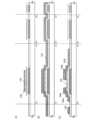
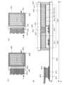
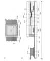
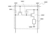
図3(A)は半導体装置の有する薄膜トランジスタ470の平面図であり、図3(B)は
図3(A)の線C1-C2における断面図である。薄膜トランジスタ470は逆スタガ型
の薄膜トランジスタであり、絶縁表面を有する基板である基板400上に、ゲート電極層
401、ゲート絶縁層402、半導体層403、ソース領域又はドレイン領域404a、
404b、及びソース電極層又はドレイン電極層405a、405bを含む。また、薄膜
トランジスタ470を覆い、半導体層403に接する酸化物絶縁膜407が設けられてい
る。3A is a plan view of a
In addition, an
半導体層403、及びソース領域又はドレイン領域404a、404bは、少なくとも第
1の酸化物半導体膜及び第2の酸化物半導体膜の成膜後に不純物である水分などを低減す
る加熱処理(脱水化または脱水素化のための加熱処理)が行われ、低抵抗化(キャリア濃
度が高まる、好ましくは1×10¹⁸/cm3以上)させた後、第1の酸化物半導体層に
酸化物絶縁膜407を接して形成することにより、高抵抗化(キャリア濃度が低まる、好
ましくは1×10¹⁸/cm3未満、さらに好ましくは1×1014/cm3以下)させ
た第1の酸化物半導体層をチャネル形成領域として用いることができる。The
さらに、脱水化または脱水素化のための加熱処理によって水分(H2O)などの不純物を
脱離させる過程を経た後、酸素雰囲気下で徐冷を行うことが好ましい。脱水化または脱水
素化のための加熱処理及び、酸素雰囲気下で徐冷させた後、第1の酸化物半導体層に接し
て酸化物絶縁膜の形成などを行って第1の酸化物半導体層のキャリア濃度を低減すること
が、薄膜トランジスタ470の信頼性の向上に繋がる。Furthermore, it is preferable to perform a process of removing impurities such as moisture (H2 O) by heat treatment for dehydration or dehydrogenation and then slowly cooling in an oxygen atmosphere. After the heat treatment for dehydration or dehydrogenation and the slow cooling in an oxygen atmosphere, an oxide insulating film is formed in contact with the first oxide semiconductor layer to reduce the carrier concentration of the first oxide semiconductor layer, which leads to improvement in reliability of the
また、半導体層403及びソース領域又はドレイン領域404a、404b内だけでなく
、ゲート絶縁層402内、及び上下に接して設けられる膜と酸化物半導体である半導体層
403の界面、具体的にはゲート絶縁層402と半導体層403の界面、及び酸化物絶縁
膜407と半導体層403の界面に存在する水分などの不純物を低減する。In addition, impurities such as moisture that are present not only in the
なお、酸化物半導体層である半導体層403、ソース領域及びドレイン領域404a、4
04bと接するソース電極層又はドレイン電極層405a、405bとして、チタン、ア
ルミニウム、マンガン、マグネシウム、ジルコニウム、ベリリウム、トリウムのいずれか
一または複数から選択された材料とする。また、上述した元素を組み合わせた合金膜など
を積層してもよい。Note that the
The source electrode layer or
チャネル形成領域を含む半導体層403及びソース領域又はドレイン領域404a、40
4bとしては、半導体特性を有する酸化物材料を用いればよい。例えば、InMO3(Z
nO)m(m>0)で表記される構造の酸化物半導体を用いることができ、特に、In-
Ga-Zn-O系酸化物半導体を用いるのが好ましい。なお、Mは、ガリウム(Ga)、
鉄(Fe)、ニッケル(Ni)、マンガン(Mn)及びコバルト(Co)から選ばれた一
の金属元素又は複数の金属元素を示す。例えばMとして、Gaの場合があることの他、G
aとNi又はGaとFeなど、Ga以外の上記金属元素が含まれる場合がある。また、上
記酸化物半導体において、Mとして含まれる金属元素の他に、不純物元素としてFe、N
i等その他の遷移金属元素、又は該遷移金属の酸化物が含まれているものがある。本明細
書においては、InMO3(ZnO)m(m>0)で表記される構造の酸化物半導体のう
ち、Mとして少なくともGaを含む構造の酸化物半導体をIn-Ga-Zn-O系酸化物
半導体と呼び、該薄膜をIn-Ga-Zn-O系非単結晶膜とも呼ぶ。A
As the material 4b, an oxide material having semiconductor properties may be used. For example, InMO3 (Z
nO)m (m>0) can be used, and in particular, an oxide semiconductor having a structure represented by In-
It is preferable to use a Ga—Zn—O-based oxide semiconductor. Note that M is gallium (Ga);
It represents one or more metal elements selected from iron (Fe), nickel (Ni), manganese (Mn) and cobalt (Co). For example, M can be Ga, or G
In addition to the metal element M, the oxide semiconductor may contain Fe, N, or the like as impurity elements.
In this specification, among oxide semiconductors having a structure represented by InMO3 (ZnO)m (m>0), an oxide semiconductor having a structure containing at least Ga as M is referred to as an In—Ga—Zn—O-based oxide semiconductor, and the thin film is also referred to as an In—Ga—Zn—O-based non-single-crystal film.
また、酸化物半導体層に適用する酸化物半導体として上記の他にも、In-Sn-Zn-
O系、In-Al-Zn-O系、Sn-Ga-Zn-O系、Al-Ga-Zn-O系、S
n-Al-Zn-O系、In-Zn-O系、Sn-Zn-O系、Al-Zn-O系、In
-O系、Sn-O系、Zn-O系の酸化物半導体を適用することができる。また上記酸化
物半導体に酸化珪素を含ませてもよい。In addition to the above, the oxide semiconductor layer can be formed using In--Sn--Zn-
O-based, In-Al-Zn-O-based, Sn-Ga-Zn-O-based, Al-Ga-Zn-O-based, S
n-Al-Zn-O system, In-Zn-O system, Sn-Zn-O system, Al-Zn-O system, In
The oxide semiconductor may be an oxide semiconductor containing silicon oxide.
半導体層(第1の酸化物半導体層ともいう)とソース電極層の間にソース領域を、半導体
層とドレイン電極層との間にドレイン領域を有する。ソース領域及びドレイン領域に、n
型の導電型を示す酸化物半導体層(第2の酸化物半導体層ともいう)を用いることができ
る。A source region is provided between the semiconductor layer (also referred to as a first oxide semiconductor layer) and the source electrode layer, and a drain region is provided between the semiconductor layer and the drain electrode layer.
For example, an oxide semiconductor layer having a first conductivity type (also referred to as a second oxide semiconductor layer) can be used.
また、薄膜トランジスタのソース領域又はドレイン領域404a、404bとして用いる
第2の酸化物半導体層は、チャネル形成領域として用いる第1の酸化物半導体層の膜厚よ
りも薄く、且つ、より高い導電率(電気伝導度)を有するのが好ましい。The second oxide semiconductor layer used as the source or drain
またチャネル形成領域として用いる第1の酸化物半導層は非晶質構造を有し、ソース領域
及びドレイン領域として用いる第2の酸化物半導体層は非晶質構造の中に結晶粒(ナノク
リスタル)を含む場合がある。このソース領域及びドレイン領域として用いる第2の酸化
物半導体層中の結晶粒(ナノクリスタル)は直径1nm~10nm、代表的には2nm~
4nm程度である。The first oxide semiconductor layer used as the channel formation region has an amorphous structure, and the second oxide semiconductor layer used as the source and drain regions may contain crystal grains (nanocrystals) in the amorphous structure. The crystal grains (nanocrystals) in the second oxide semiconductor layer used as the source and drain regions have a diameter of 1 nm to 10 nm, typically 2 nm to 40 nm.
It is about 4 nm.
本実施の形態では、チャネル形成領域を含む半導体層403、及びソース領域又はドレイ
ン領域(n+層、バッファ層ともいう)404a、404bとしてIn-Ga-Zn-O
系非単結晶膜を用いる。In this embodiment, the
A non-single crystal film based on the GaN-based ...
図1及び図2に薄膜トランジスタ470の作製工程の断面図を示す。Figures 1 and 2 show cross-sectional views of the manufacturing process of
絶縁表面を有する基板である基板400上にゲート電極層401を設ける。下地膜となる
絶縁膜を基板400とゲート電極層401の間に設けてもよい。下地膜は、基板400か
らの不純物元素の拡散を防止する機能があり、窒化珪素膜、酸化珪素膜、窒化酸化珪素膜
、又は酸化窒化珪素膜から選ばれた一又は複数の膜による積層構造により形成することが
できる。ゲート電極層401の材料は、モリブデン、チタン、クロム、タンタル、タング
ステン、アルミニウム、銅、ネオジム、スカンジウム等の金属材料又はこれらを主成分と
する合金材料を用いて、単層で又は積層して形成することができる。A
例えば、ゲート電極層401の2層の積層構造としては、アルミニウム層上にモリブデン
層が積層された2層の積層構造、または銅層上にモリブデン層を積層した2層構造、また
は銅層上に窒化チタン層若しくは窒化タンタル層を積層した2層構造、窒化チタン層とモ
リブデン層とを積層した2層構造とすることが好ましい。3層の積層構造としては、タン
グステン層または窒化タングステン層と、アルミニウムと珪素の合金層またはアルミニウ
ムとチタンの合金層と、窒化チタン層またはチタン層とを積層した積層とすることが好ま
しい。For example, the two-layer stacked structure of the
ゲート電極層401上にゲート絶縁層402を形成する。A
ゲート絶縁層402は、プラズマCVD法又はスパッタリング法等を用いて、酸化珪素層
、窒化珪素層、酸化窒化珪素層又は窒化酸化珪素層を単層で又は積層して形成することが
できる。例えば、成膜ガスとして、SiH4、酸素及び窒素を用いてプラズマCVD法に
より酸化窒化珪素層を形成すればよい。The
ゲート絶縁層402上に、第1の酸化物半導体膜430及び第2の酸化物半導体膜433
を積層して形成する(図1(A)参照。)。第1の酸化物半導体膜430はチャネル形成
領域として機能する半導体層に、第2の酸化物半導体膜433はソース領域及びドレイン
領域となる。A first
The first
なお、酸化物半導体膜をスパッタ法により成膜する前に、アルゴンガスを導入してプラズ
マを発生させる逆スパッタを行い、ゲート絶縁層402の表面に付着しているゴミを除去
することが好ましい。逆スパッタとは、ターゲット側に電圧を印加せずに、アルゴン雰囲
気下で基板側にRF電源を用いて電圧を印加して基板近傍にプラズマを形成して表面を改
質する方法である。なお、アルゴン雰囲気に代えて窒素、ヘリウムなどを用いてもよい。
また、アルゴン雰囲気に酸素、N2Oなどを加えた雰囲気で行ってもよい。また、アルゴ
ン雰囲気にCl2、CF4などを加えた雰囲気で行ってもよい。Note that before the oxide semiconductor film is formed by a sputtering method, it is preferable to perform reverse sputtering in which argon gas is introduced to generate plasma and remove dust attached to the surface of the
Alternatively, the treatment may be performed in an atmosphere in which oxygen, N2 O, etc. are added to an argon atmosphere, or in which Cl2 , CF4 , etc. are added to an argon atmosphere.
酸化物半導体膜としてIn-Ga-Zn-O系非単結晶膜を用いる。酸化物半導体膜は、
In-Ga-Zn-O系酸化物半導体ターゲットを用いてスパッタ法により成膜する。ま
た、酸化物半導体膜は、希ガス(代表的にはアルゴン)雰囲気下、酸素雰囲気下、又は希
ガス(代表的にはアルゴン)及び酸素雰囲気下においてスパッタ法により形成することが
できる。An In—Ga—Zn—O-based non-single-crystal film is used as the oxide semiconductor film.
The oxide semiconductor film is formed by a sputtering method using an In—Ga—Zn—O-based oxide semiconductor target. The oxide semiconductor film can be formed by a sputtering method in a rare gas (typically, argon) atmosphere, an oxygen atmosphere, or an atmosphere of rare gas (typically, argon) and oxygen.
ゲート絶縁層402、第1の酸化物半導体膜430、及び第2の酸化物半導体膜433を
大気に触れさせることなく連続的に形成してもよい。大気に触れさせることなく連続成膜
することで、界面が、水やハイドロカーボンなどの、大気成分や大気中に浮遊する不純物
元素に汚染されることなく各積層界面を形成することができるので、薄膜トランジスタ特
性のばらつきを低減することができる。The
第1の酸化物半導体膜430及び第2の酸化物半導体膜433に不活性ガス雰囲気(窒素
、またはヘリウム、ネオン、アルゴン等)下或いは減圧下において加熱処理を行った後、
酸素雰囲気下で徐冷を行う(図1(B)参照。)。第1の酸化物半導体膜430及び第2
の酸化物半導体膜433を上記雰囲気下で加熱処理することで、第1の酸化物半導体膜4
30及び第2の酸化物半導体膜433に含まれる水素及び水などの不純物を除去すること
ができる。The first
The first
The
Impurities such as hydrogen and water contained in the
なお、加熱処理においては、窒素、またはヘリウム、ネオン、アルゴン等の希ガスに、水
、水素などの不純物が含まれないことが好ましい。または、加熱処理装置に導入する窒素
、またはヘリウム、ネオン、アルゴン等の希ガスの純度を、6N(99.9999%)以
上、好ましくは7N(99.99999%)以上、(即ち不純物濃度を1ppm以下、好
ましくは0.1ppm以下)とすることが好ましい。In the heat treatment, it is preferable that impurities such as water, hydrogen, etc. are not contained in nitrogen or a rare gas such as helium, neon, or argon. Alternatively, it is preferable that the purity of nitrogen or a rare gas such as helium, neon, or argon introduced into the heat treatment device is 6N (99.9999%) or more, preferably 7N (99.99999%) or more (i.e., the impurity concentration is 1 ppm or less, preferably 0.1 ppm or less).
また、加熱処理は、電気炉を用いた加熱方法、加熱した気体を用いるGRTA(Gas
Rapid Thermal Anneal)法またはランプ光を用いるLRTA(La
mp Rapid Thermal Anneal)法などの瞬間加熱方法などを用いる
ことができる。The heat treatment may be performed by a heating method using an electric furnace or a GRTA (Gas Reactor-Transporter) method using heated gas.
Rapid Thermal Anneal (LRTA) method or lamp light
For example, a rapid heating method such as a Rapid Thermal Anneal method can be used.
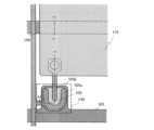
ここで、第1の酸化物半導体膜430及び第2の酸化物半導体膜433の加熱処理の一形
態として、電気炉601を用いた加熱方法について、図28を用いて説明する。Here, as one mode of heat treatment of the first
図28は、電気炉601の概略図である。チャンバー602の外側にはヒーター603が
設けられており、チャンバー602を加熱する。また、チャンバー602内には、基板6
04を搭載するサセプター605が設けられており、チャンバー602内に基板604を
搬入または搬出する。また、チャンバー602にはガス供給手段606及び排気手段60
7が設けられている。ガス供給手段606により、チャンバー602にガスを導入する。
また、排気手段607により、チャンバー602内を排気する、またはチャンバー602
内を減圧にする。なお、電気炉601の昇温特性を0.1℃/min以上20℃/min
以下とすることが好ましい。また、電気炉601の降温特性を0.1℃/min以上15
℃/min以下とすることが好ましい。28 is a schematic diagram of an
A
7 is provided. Gas is introduced into the
In addition, the inside of the
The inside of the
It is preferable that the temperature drop rate of the
It is preferable to set the rate to .degree. C./min or less.
ガス供給手段606は、ガス供給源611a、ガス供給源611b、圧力調整弁612a
、圧力調整弁612b、精製器613a、精製器613b、マスフローコントローラ61
4a、マスフローコントローラ614b、ストップバルブ615a、ストップバルブ61
5bを有する。本実施の形態では、ガス供給源611a、ガス供給源611bとチャンバ
ー602の間に精製器613a、精製器613bを設けることが好ましい。精製器613
a、精製器613b、を設けることで、ガス供給源611a、ガス供給源611bからチ
ャンバー602内に導入されるガスの、水、水素などの不純物を、当該精製器613a、
精製器613bによって除去することで、チャンバー602内への水、水素などの侵入を
低減することができる。The gas supply means 606 includes a
,
4a,
In this embodiment, it is preferable to provide a
By providing the
By removing them using the
本実施の形態では、ガス供給源611a、ガス供給源611bから、窒素または希ガスを
チャンバー602に導入し、チャンバー内を窒素または希ガス雰囲気とし、200℃以上
600℃以下、好ましくは400℃以上450℃以下に加熱されたチャンバー602にお
いて、基板604上に形成された第1の酸化物半導体膜430及び第2の酸化物半導体膜
433を加熱することで、第1の酸化物半導体膜430及び第2の酸化物半導体膜433
の脱水化または脱水素化を行うことができる。In this embodiment, nitrogen or a rare gas is introduced into the
The above can be subjected to dehydration or dehydrogenation.
または、排気手段による減圧下で、200℃以上600℃以下、好ましくは400℃以上
450℃以下に加熱されたチャンバー602において、基板604上に形成された第1の
酸化物半導体膜430及び第2の酸化物半導体膜433を加熱することで、第1の酸化物
半導体膜430及び第2の酸化物半導体膜433の脱水化または脱水素化を行うことがで
きる。Alternatively, the first
次に、ガス供給源611aから窒素または希ガスをチャンバー602への導入を止めると
共に、ヒーターをオフ状態にする。次に、ガス供給源611bから酸素をチャンバー60
2内に導入し、加熱装置のチャンバー602を徐々に冷却する。即ち、チャンバー602
内を酸素雰囲気とし、基板604を徐々に冷却する。ここでは、ガス供給源611bから
チャンバー602内に導入する酸素に、水、水素などの不純物が含まれないことが好まし
い。または、ガス供給源611bからチャンバー602内に導入する酸素の純度を6N(
99.9999%)以上、好ましくは7N(99.99999%)以上、(即ち、酸素中
の不純物濃度を1ppm以下、好ましくは0.1ppm以下)とすることが好ましい。酸
化物半導体膜は不活性ガス雰囲気下或いは減圧下における加熱処理によって、低抵抗化(
キャリア濃度が高まる、好ましくは1×10¹⁸/cm3以上)し、低抵抗化した第1の
酸化物半導体膜434及び第2の酸化物半導体膜435とすることができる。Next, the introduction of nitrogen or rare gas from the
2, and the
The inside of the
The oxide semiconductor film is preferably made to have a low resistance (
The first
この結果、後に形成される薄膜トランジスタの信頼性を高めることができる。As a result, the reliability of the thin-film transistors that will be formed later can be improved.
なお、減圧下で加熱処理を行った場合は、加熱処理後にチャンバー602に酸素を流して
圧力を大気圧に戻して冷却すればよい。When the heat treatment is performed under reduced pressure, oxygen may be flowed into the
また、ガス供給源611bから酸素をチャンバー602に導入すると同時に、ヘリウム、
ネオン、アルゴンなどの希ガスまたは窒素の一方または両方をチャンバー602内に導入
してもよい。In addition, oxygen is introduced into the
A noble gas such as neon, argon, or nitrogen, or both, may be introduced into the
また、加熱装置のチャンバー602内の基板604を300℃まで冷却した後、基板60
4を室温の雰囲気に移動してもよい。この結果、基板604の冷却時間を短縮することが
できる。After the
4 may be moved to a room temperature atmosphere, thereby shortening the cooling time of the
また、加熱装置がマルチチャンバーの場合、加熱処理と冷却処理を異なるチャンバーで行
うことができる。代表的には、窒素または希ガスが充填され、且つ200℃以上600℃
以下、好ましくは400℃以上450℃以下に加熱された第1のチャンバーにおいて、基
板上の酸化物半導体膜を加熱する。次に、窒素または希ガスが導入された搬送室を経て、
酸素が充填され、且つ100℃以下、好ましくは室温である第2のチャンバーに、上記加
熱処理された基板を移動し、冷却処理を行う。以上の工程により、スループットを向上さ
せることができる。In addition, when the heating device has a multi-chamber, the heating process and the cooling process can be performed in different chambers.
The oxide semiconductor film on the substrate is heated in a first chamber that is preferably heated to a temperature of greater than or equal to 400° C. and less than or equal to 450° C. Next, the oxide semiconductor film is transferred to a transfer chamber into which nitrogen or a rare gas is introduced.
The substrate that has been subjected to the heat treatment is transferred to a second chamber that is filled with oxygen and has a temperature of 100° C. or less, preferably room temperature, and is then cooled. Throughput can be improved by the above steps.
不活性ガス雰囲気下或いは減圧下における加熱処理後に、酸素雰囲気下で室温以上100
℃未満まで徐冷を行い、第1の酸化物半導体膜434及び第2の酸化物半導体膜435が
設けられ¥た基板を加熱装置から取り出し、フォトリソグラフィ工程を行う。After heat treatment in an inert gas atmosphere or under reduced pressure, the mixture is heated at room temperature or above for 100
C., the substrate on which the first
また、不活性ガス雰囲気下或いは減圧下の加熱処理後の第1の酸化物半導体膜434及び
第2の酸化物半導体膜435の状態は、非晶質な状態であることが好ましいが、一部結晶
化してもよい。The first
第1の酸化物半導体膜434及び第2の酸化物半導体膜435をフォトリソグラフィ工程
により島状の酸化物半導体層である第1の酸化物半導体層431、第2の酸化物半導体層
436に加工する(図1(C)参照。)。The first
ゲート絶縁層402、第1の酸化物半導体層431、及び第2の酸化物半導体層436上
に導電膜を形成する。A conductive film is formed over the
導電膜の材料としては、Al、Cr、Ta、Ti、Mo、Wから選ばれた元素、または上
述した元素を成分とする合金か、上述した元素を組み合わせた合金膜等が挙げられる。The material of the conductive film may be an element selected from Al, Cr, Ta, Ti, Mo, or W, or an alloy containing the above elements, or an alloy film of a combination of the above elements.
また、導電膜の形成後に加熱処理を行う場合には、この加熱処理に耐える耐熱性を導電膜
に持たせることが好ましい。Al単体では耐熱性が劣り、また腐蝕しやすい等の問題点が
あるので耐熱性導電性材料と組み合わせて形成する。Alと組み合わせる耐熱性導電性材
料としては、チタン(Ti)、タンタル(Ta)、タングステン(W)、モリブデン(M
o)、クロム(Cr)、Nd(ネオジム)、Sc(スカンジウム)から選ばれた元素、ま
たは上述した元素を成分とする合金か、上述した元素を組み合わせた合金膜、または上述
した元素を成分とする窒化物で形成する。In addition, when a heat treatment is performed after the formation of the conductive film, it is preferable that the conductive film has heat resistance that can withstand this heat treatment. Since Al alone has problems such as poor heat resistance and is easily corroded, it is formed in combination with a heat-resistant conductive material. Examples of heat-resistant conductive materials that can be combined with Al include titanium (Ti), tantalum (Ta), tungsten (W), molybdenum (Mo), and the like.
The insulating layer is formed of an element selected from the group consisting of chromium (Zn), chromium (Cr), neodymium (Nd), and scandium (Sc), or an alloy containing the above-mentioned elements, an alloy film combining the above-mentioned elements, or a nitride containing the above-mentioned elements.
第1の酸化物半導体層431、及び第2の酸化物半導体層436、導電膜をエッチング工
程によりエッチングし、第1の酸化物半導体層432、及びソース領域又はドレイン領域
404a、404b、及びソース電極層又はドレイン電極層405a、405bを形成す
る(図2(A)参照。)。なお、第1の酸化物半導体層431は一部のみがエッチングさ
れ、溝部(凹部)を有する第1の酸化物半導体層432となる。The first
第1の酸化物半導体層432に接してスパッタ法による酸化珪素膜を酸化物絶縁膜407
として形成する。低抵抗化した酸化物半導体層に接して形成する酸化物絶縁膜407は、
水分や、水素イオンや、OH-などの不純物を含まず、これらが外部から侵入することを
ブロックする無機絶縁膜を用い、具体的には酸化珪素膜、または窒化酸化珪素膜を用いる
。A silicon oxide film is formed in contact with the first
The
An inorganic insulating film that does not contain impurities such as moisture, hydrogen ions, and OH− and blocks the intrusion of these from the outside is used, specifically a silicon oxide film or a silicon nitride oxide film.
本実施の形態では、酸化物絶縁膜407として膜厚300nmの酸化珪素膜を成膜する。
成膜時の基板温度は、室温以上300℃以下とすればよく、本実施の形態では100℃と
する。酸化珪素膜のスパッタ法による成膜は、希ガス(代表的にはアルゴン)雰囲気下、
酸素雰囲気下、又は希ガス(代表的にはアルゴン)及び酸素雰囲気下において行うことが
できる。また、ターゲットとして酸化珪素ターゲットを用いても珪素ターゲットを用いて
もよい。例えば珪素ターゲットを用いて、酸素、及び窒素雰囲気下でスパッタ法により酸
化珪素膜を形成することができる。In this embodiment, a silicon oxide film is formed to a thickness of 300 nm as the
The substrate temperature during film formation may be from room temperature to 300° C. inclusive, and in this embodiment mode, is set to 100° C. The silicon oxide film is formed by sputtering in a rare gas (typically argon) atmosphere.
The sputtering can be performed in an oxygen atmosphere or in an atmosphere of a rare gas (typically argon) and oxygen. A silicon oxide target or a silicon target may be used as the target. For example, a silicon oxide film can be formed by sputtering in an atmosphere of oxygen and nitrogen using a silicon target.
低抵抗化した第1の酸化物半導体層432に接してスパッタ法またはPCVD法などによ
り酸化物絶縁膜407を形成すると、低抵抗化した第1の酸化物半導体層432において
少なくとも酸化物絶縁膜407と接する領域を高抵抗化(キャリア濃度が低まる、好まし
くは1×10¹⁸/cm3未満、さらに好ましくは1×1014/cm3以下)し、高抵
抗化酸化物半導体領域とすることができる。半導体装置の作製プロセス中、不活性気体雰
囲気下(或いは減圧下)での加熱、酸素雰囲気下での徐冷及び酸化物絶縁膜の形成などに
よって酸化物半導体層のキャリア濃度を増減させることが重要である。第1の酸化物半導
体層432は、高抵抗化酸化物半導体領域を有する半導体層403となり、薄膜トランジ
スタ470を作製することができる(図2(B)参照。)。When the
上記脱水処理または脱水素処理のための加熱処理を行うことによって第1の酸化物半導体
膜及び第2の酸化物半導体膜に含まれる不純物(H2O、H、OHなど)を低減してキャ
リア濃度を増加させた後、酸素雰囲気下で徐冷を行う。徐冷させた後、第1の酸化物半導
体膜を島状の第1の酸化物半導体層に加工し、第1の酸化物半導体層に接して酸化物絶縁
膜の形成などを行って第1の酸化物半導体層のキャリア濃度を低減し半導体層として用い
ることによって、薄膜トランジスタ470の信頼性を向上することができる。By performing the heat treatment for the dehydration or dehydrogenation treatment, impurities (such as H2 O, H, or OH) contained in the first oxide semiconductor film and the second oxide semiconductor film are reduced to increase the carrier concentration, and then the film is slowly cooled in an oxygen atmosphere. After the heat treatment, the first oxide semiconductor film is processed into an island-shaped first oxide semiconductor layer, and an oxide insulating film is formed in contact with the first oxide semiconductor layer to reduce the carrier concentration of the first oxide semiconductor layer and use the first oxide semiconductor layer as a semiconductor layer, which can improve the reliability of the
また、酸化物絶縁膜407を形成後、窒素雰囲気下、又は大気雰囲気下(大気中)におい
て薄膜トランジスタ470に加熱処理(好ましくは150℃以上350℃未満)を行って
もよい。例えば、窒素雰囲気下で250℃、1時間の加熱処理を行う。該加熱処理を行う
と、半導体層403が酸化物絶縁膜407と接した状態で加熱されることになり、薄膜ト
ランジスタ470の電気的特性のばらつきを軽減することができる。この加熱処理(好ま
しくは150℃以上350℃未満)は、酸化物絶縁膜407の形成後であれば特に限定さ
れず、他の工程、例えば樹脂膜形成時の加熱処理や、透明導電膜を低抵抗化させるための
加熱処理と兼ねることで、工程数を増やすことなく行うことができる。After the
(実施の形態2)
半導体装置及び半導体装置の作製方法を、図26を用いて説明する。実施の形態1と同一
部分又は同様な機能を有する部分、及び工程は、実施の形態1と同様に行うことができ、
繰り返しの説明は省略する。(Embodiment 2)
A semiconductor device and a manufacturing method thereof will be described with reference to FIG. 26. Portions and steps having the same functions as those in
A repeated explanation will be omitted.
図26に示す薄膜トランジスタ471はゲート電極層401及び半導体層403のチャネ
ル領域に重なるように絶縁膜を介して導電層408を設ける例である。A
図26は半導体装置の有する薄膜トランジスタ471の断面図である。薄膜トランジスタ
471はボトムゲート型の薄膜トランジスタであり、絶縁表面を有する基板である基板4
00上に、ゲート電極層401、ゲート絶縁層402、半導体層403、ソース領域又は
ドレイン領域404a、404b、及びソース電極層又はドレイン電極層405a、40
5b、導電層408を含む。導電層408は、ゲート電極層401と重なるように、酸化
物絶縁膜407上に設けられている。26 is a cross-sectional view of a
400, a
5b includes a
導電層408は、ゲート電極層401、ソース電極層又はドレイン電極層405a、40
5bと同様な材料、方法を用いて形成することができる。画素電極層を設ける場合は、画
素電極層と同様な材料、方法を用いて形成してもよい。本実施の形態では、導電層408
としてチタン膜、アルミニウム膜、及びチタン膜の積層を用いる。The
In the case where a pixel electrode layer is provided, the
A stack of a titanium film, an aluminum film, and a titanium film is used as the insulating film.
導電層408は、電位がゲート電極層401と同じでもよいし、異なっていても良く、第
2のゲート電極層として機能させることもできる。また、導電層408がフローティング
状態であってもよい。The
導電層408を半導体層403と重なる位置に設けることによって、薄膜トランジスタの
信頼性を調べるためのバイアス-熱ストレス試験(以下、BT試験という)において、B
T試験前後における薄膜トランジスタ471のしきい値電圧の変化量を低減することがで
きる。特に、基板温度を150℃まで上昇させた後にゲートに印加する電圧を-20Vと
する-BT試験においてしきい値電圧の変動を抑えることができる。By providing the
It is possible to reduce the amount of change in the threshold voltage of the
本実施の形態は、実施の形態1と適宜組み合わせて実施することが可能である。This embodiment can be implemented in appropriate combination with
(実施の形態3)
半導体装置及び半導体装置の作製方法を、図27を用いて説明する。実施の形態1と同一
部分又は同様な機能を有する部分、及び工程は、実施の形態1と同様に行うことができ、
繰り返しの説明は省略する。(Embodiment 3)
A semiconductor device and a manufacturing method thereof will be described with reference to FIG. 27. A portion and a process having the same function as those in
A repeated explanation will be omitted.
図27に示す薄膜トランジスタ472はゲート電極層401及び半導体層403のチャネ
ル領域に重なるように酸化物絶縁膜407及び絶縁層410を介して導電層409を設け
る例である。A
図27は半導体装置の有する薄膜トランジスタ472の断面図である。薄膜トランジスタ
472はボトムゲート型の薄膜トランジスタであり、絶縁表面を有する基板である基板4
00上に、ゲート電極層401、ゲート絶縁層402、半導体層403、ソース領域又は
ドレイン領域404a、404b、及びソース電極層又はドレイン電極層405a、40
5b、導電層409を含む。導電層409は、ゲート電極層401と重なるように、酸化
物絶縁膜407及び絶縁層410上に設けられている。27 is a cross-sectional view of a
400, a
5b includes a
本実施の形態では、酸化物絶縁膜407上に平坦化膜として機能する絶縁層410を積層
し、酸化物絶縁膜407及び絶縁層410にソース電極層又はドレイン電極層405bに
達する開口を形成する。酸化物絶縁膜407及び絶縁層410に形成された開口及び絶縁
層410上に導電膜を形成し、所望の形状にエッチングして導電層409及び画素電極層
411を形成する。このように画素電極層411を形成する工程で、同様の材料及び方法
を用いて導電層409を形成することができる。本実施の形態では、画素電極層411、
導電層409として酸化珪素を含む酸化インジウム酸化スズ合金(酸化珪素を含むIn-
Sn-O系酸化物)を用いる。In this embodiment, an insulating
The
Sn--O oxide) is used.
また、導電層409は、ゲート電極層401、ソース電極層又はドレイン電極層405a
、405bと同様な材料、方法を用いて形成してもよい。The
, 405b may be formed using the same material and method.
導電層409は、電位がゲート電極層401と同じでもよいし、異なっていても良く、第
2のゲート電極層として機能させることもできる。また、導電層409がフローティング
状態であってもよい。The
導電層409を半導体層403と重なる位置に設けることによって、薄膜トランジスタの
信頼性を調べるためのバイアス-熱ストレス試験(以下、BT試験という)において、B
T試験前後における薄膜トランジスタ472のしきい値電圧の変化量を低減することがで
きる。By providing the
The amount of change in the threshold voltage of the
本実施の形態は、他の実施の形態に記載した構成と適宜組み合わせて実施することが可能
である。This embodiment mode can be implemented in appropriate combination with structures described in other embodiment modes.
(実施の形態4)
薄膜トランジスタを含む半導体装置の作製工程について、図4乃至図8を用いて説明する
。(Embodiment 4)
A manufacturing process of a semiconductor device including a thin film transistor will be described with reference to FIGS.
図4(A)において、透光性を有する基板100にはバリウムホウケイ酸ガラスやアルミ
ノホウケイ酸ガラスなどのガラス基板を用いることができる。In FIG. 4A, a glass substrate such as barium borosilicate glass or aluminoborosilicate glass can be used as a light-transmitting
次いで、導電層を基板100全面に形成した後、第1のフォトリソグラフィ工程を行い、
レジストマスクを形成し、エッチングにより不要な部分を除去して配線及び電極(ゲート
電極層101を含むゲート配線、容量配線108、及び第1の端子121)を形成する。
このとき少なくともゲート電極層101の端部にテーパーが形成されるようにエッチング
する。Next, a conductive layer is formed on the entire surface of the
A resist mask is formed, and unnecessary portions are removed by etching to form wirings and electrodes (a gate wiring including the
At this time, etching is performed so that at least the end of the
ゲート電極層101を含むゲート配線と容量配線108、端子部の第1の端子121は、
耐熱性導電性材料であるチタン(Ti)、タンタル(Ta)、タングステン(W)、モリ
ブデン(Mo)、クロム(Cr)、Nd(ネオジム)、スカンジウム(Sc)から選ばれ
た元素、または上述した元素を成分とする合金か、上述した元素を組み合わせた合金膜、
または上述した元素を成分とする窒化物で形成することが望ましい。また、アルミニウム
(Al)や銅(Cu)などの低抵抗導電性材料で形成する場合は、Al単体あるいはCu
単体では耐熱性が劣り、また腐蝕しやすい等の問題点があるので上記耐熱性導電性材料と
組み合わせて形成する。The gate wiring including the
An element selected from the group consisting of heat-resistant conductive materials titanium (Ti), tantalum (Ta), tungsten (W), molybdenum (Mo), chromium (Cr), neodymium (Nd), and scandium (Sc), or an alloy containing the above elements as components, or an alloy film combining the above elements,
Alternatively, it is preferable to form the insulating layer 11 from a nitride containing the above-mentioned elements. When the insulating layer 11 is formed from a low-resistance conductive material such as aluminum (Al) or copper (Cu), the insulating layer 11 is preferably formed from a single element of Al or a single element of Cu.
Since the metal foil alone has problems such as poor heat resistance and susceptibility to corrosion, it is formed in combination with the above heat-resistant conductive material.
次いで、ゲート電極層101上にゲート絶縁層102を全面に成膜する(図4(A)参照
。)。ゲート絶縁層102はスパッタ法、PCVD法などを用い、膜厚を50~250n
mとする。Next, a
Let m.
例えば、ゲート絶縁層102としてスパッタ法により酸化珪素膜を用い、100nmの厚
さで形成する。勿論、ゲート絶縁層102はこのような酸化珪素膜に限定されるものでな
く、酸化窒化珪素膜、窒化珪素膜、酸化アルミニウム膜、酸化タンタル膜などの他の絶縁
膜を用い、これらの材料から成る単層または積層構造として形成しても良い。For example, a silicon oxide film is formed by a sputtering method to a thickness of 100 nm as the
次に、ゲート絶縁層102上に、第1の酸化物半導体膜131(第1のIn-Ga-Zn
-O系非単結晶膜)を成膜する。プラズマ処理後、大気に曝すことなく第1の酸化物半導
体膜131を成膜することは、ゲート絶縁層と半導体膜の界面にゴミや水分を付着させな
い点で有用である。ここでは、直径8インチのIn、Ga、及びZnを含む酸化物半導体
ターゲット(In2O3:Ga2O3:ZnO=1:1:1)を用いて、基板とターゲッ
トの間との距離を170mm、圧力0.4Pa、直流(DC)電源0.5kW、アルゴン
又は酸素雰囲気下で成膜する。なお、パルス直流(DC)電源を用いると、ごみが軽減で
き、膜厚分布も均一となるために好ましい。第1の酸化物半導体膜131の膜厚は、5n
m~200nmとする。第1の酸化物半導体膜131として、In-Ga-Zn-O系酸
化物半導体ターゲットを用いてスパッタ法により膜厚50nmのIn-Ga-Zn-O系
非単結晶膜を成膜する。Next, a first oxide semiconductor film 131 (first In—Ga—Zn
A -O-based non-single crystal film) is formed. After the plasma treatment, the first
As the first
次いで、大気に曝すことなく、第2の酸化物半導体膜136(第2のIn-Ga-Zn-
O系非単結晶膜)をスパッタ法で成膜する(図4(B)参照。)。ここでは、In2O3
:Ga2O3:ZnO=1:1:1としたターゲットを用い、成膜条件は、圧力を0.4
Paとし、電力を500Wとし、成膜温度を室温とし、アルゴンガス流量40sccmを
導入してスパッタ成膜を行う。In2O3:Ga2O3:ZnO=1:1:1としたター
ゲットを用いているにも関わらず、成膜直後で大きさ1nm~10nmの結晶粒を含むI
n-Ga-Zn-O系非単結晶膜が形成されることがある。なお、ターゲットの成分比、
成膜圧力(0.1Pa~2.0Pa)、電力(250W~3000W:8インチφ)、温
度(室温~100℃)、反応性スパッタの成膜条件などを適宜調節することで結晶粒の有
無や、結晶粒の密度や、直径サイズは、1nm~10nmの範囲で調節されうると言える
。第2のIn-Ga-Zn-O系非単結晶膜の膜厚は、5nm~20nmとする。勿論、
膜中に結晶粒が含まれる場合、含まれる結晶粒のサイズが膜厚を超える大きさとならない
。第2のIn-Ga-Zn-O系非単結晶膜の膜厚は、5nmとする。Next, a second oxide semiconductor film 136 (a second In—Ga—Zn—
In this example, a non-single crystal film of In2 O3 is formed by sputtering (see FIG. 4B).
The film was formed using a target of Ga2 O3 :ZnO=1:1:1 under the following conditions: pressure of 0.4
The sputtering deposition was performed ata pressureof500 Pa, a power of 500 W, a deposition temperature of room temperature, and an argon gas flow rate of40 sccm.
In some cases, a non-single crystal film of n-Ga-Zn-O system may be formed.
By appropriately adjusting the film formation pressure (0.1 Pa to 2.0 Pa), power (250 W to 3000 W: 8 inches φ), temperature (room temperature to 100° C.), film formation conditions of reactive sputtering, etc., it can be said that the presence or absence of crystal grains, the density of crystal grains, and the diameter size can be adjusted in the range of 1 nm to 10 nm. The film thickness of the second In—Ga—Zn—O based non-single crystal film is set to 5 nm to 20 nm. Of course,
When crystal grains are contained in the film, the size of the contained crystal grains does not exceed the thickness of the film. The thickness of the second In-Ga-Zn-O based non-single crystal film is set to 5 nm.
第1のIn-Ga-Zn-O系非単結晶膜は、第2のIn-Ga-Zn-O系非単結晶膜
の成膜条件と異ならせる。例えば、第2のIn-Ga-Zn-O系非単結晶膜の成膜条件
における酸素ガス流量とアルゴンガス流量の比よりも第1のIn-Ga-Zn-O系非単
結晶膜の成膜条件における酸素ガス流量の占める比率が多い条件とする。具体的には、第
2のIn-Ga-Zn-O系非単結晶膜の成膜条件は、希ガス(アルゴン、又はヘリウム
など)雰囲気下(または酸素ガス10%以下、アルゴンガス90%以上)とし、第1のI
n-Ga-Zn-O系非単結晶膜の成膜条件は、酸素混合雰囲気下(酸素ガス流量は希ガ
ス流量より多い)とする。The deposition conditions for the first In-Ga-Zn-O-based non-single crystal film are made different from those for the second In-Ga-Zn-O-based non-single crystal film. For example, the ratio of the oxygen gas flow rate in the deposition conditions for the first In-Ga-Zn-O-based non-single crystal film is made higher than the ratio of the oxygen gas flow rate to the argon gas flow rate in the deposition conditions for the second In-Ga-Zn-O-based non-single crystal film. Specifically, the deposition conditions for the second In-Ga-Zn-O-based non-single crystal film are made under a rare gas (argon, helium, etc.) atmosphere (or
The condition for forming the n-Ga-Zn-O based non-single crystal film is an oxygen mixed atmosphere (oxygen gas flow rate is higher than the rare gas flow rate).
第2のIn-Ga-Zn-O系非単結晶膜の成膜は、先に逆スパッタを行ったチャンバー
と同一チャンバーを用いてもよいし、先に逆スパッタを行ったチャンバーと異なるチャン
バーで成膜してもよい。The second In--Ga--Zn--O based non-single crystal film may be formed in the same chamber as the previous reverse sputtering, or in a chamber different from the previous reverse sputtering.
スパッタ法にはスパッタ用電源に高周波電源を用いるRFスパッタ法と、DCスパッタ法
があり、さらにパルス的にバイアスを与えるパルスDCスパッタ法もある。RFスパッタ
法は主に絶縁膜を成膜する場合に用いられ、DCスパッタ法は主に金属膜を成膜する場合
に用いられる。There are two types of sputtering: RF sputtering, which uses a high-frequency power source as the sputtering power source, and DC sputtering, which also has a pulsed DC sputtering method that applies a bias in a pulsed manner. RF sputtering is mainly used when depositing insulating films, and DC sputtering is mainly used when depositing metal films.
また、材料の異なるターゲットを複数設置できる多元スパッタ装置もある。多元スパッタ
装置は、同一チャンバーで異なる材料膜を積層成膜することも、同一チャンバーで複数種
類の材料を同時に放電させて成膜することもできる。There are also multi-target sputtering devices that can accommodate multiple targets of different materials. Multi-target sputtering devices can deposit layers of different materials in the same chamber, or deposit films by discharging multiple types of materials simultaneously in the same chamber.
また、チャンバー内部に磁石機構を備えたマグネトロンスパッタ法を用いるスパッタ装置
や、グロー放電を使わずマイクロ波を用いて発生させたプラズマを用いるECRスパッタ
法を用いるスパッタ装置がある。There are also sputtering devices that use a magnetron sputtering method equipped with a magnet mechanism inside the chamber, and sputtering devices that use an ECR sputtering method that uses plasma generated by microwaves without using glow discharge.
また、スパッタ法を用いる成膜方法として、成膜中にターゲット物質とスパッタガス成分
とを化学反応させてそれらの化合物薄膜を形成するリアクティブスパッタ法や、成膜中に
基板にも電圧をかけるバイアススパッタ法もある。Other examples of film formation methods using sputtering include reactive sputtering, which forms a compound thin film by chemically reacting a target material with sputtering gas components during film formation, and bias sputtering, which also applies a voltage to the substrate during film formation.
次に、第1の酸化物半導体膜131及び第2の酸化物半導体膜136に脱水化または脱水
素化のための加熱処理を行う。第1の酸化物半導体膜131及び第2の酸化物半導体膜1
36に不活性ガス雰囲気(窒素、またはヘリウム、ネオン、アルゴン等)下或いは減圧下
において加熱処理を行った後、酸素雰囲気下で徐冷を行う。Next, heat treatment is performed on the first
After heat treatment in an inert gas atmosphere (nitrogen, helium, neon, argon, or the like) or under reduced pressure, the substrate 36 is slowly cooled in an oxygen atmosphere.
加熱処理は、200℃以上で行うと良い。例えば、窒素雰囲気下で450℃、1時間の加
熱処理を行う。この窒素雰囲気下の加熱処理により、第1の酸化物半導体膜131及び第
2の酸化物半導体膜136は、低抵抗化(キャリア濃度が高まる、好ましくは1×101
8/cm3以上)し導電率が高まる。よって低抵抗化した第1の酸化物半導体膜133及
び第2の酸化物半導体膜137が形成される(図4(C)参照。)。第1の酸化物半導体
膜133及び第2の酸化物半導体膜137の電気伝導率は1×10⁻¹S/cm以上1×
102S/cm以下が好ましい。The heat treatment is preferably performed at 200° C. or higher. For example, the heat treatment is performed at 450° C. for 1 hour in a nitrogen atmosphere. By this heat treatment in a nitrogen atmosphere, the resistance of the first
8 /cm3 or more) and the electrical conductivity is increased. As a result, the first
A value of 102 S/cm or less is preferred.
次に、第2のフォトリソグラフィ工程を行い、レジストマスクを形成し、第1の酸化物半
導体膜133及び第2の酸化物半導体膜137をエッチングする。例えば燐酸と酢酸と硝
酸を混ぜた溶液を用いたウェットエッチングにより、不要な部分を除去して第1の酸化物
半導体層134及び第2の酸化物半導体層138を形成する。なお、ここでのエッチング
は、ウェットエッチングに限定されずドライエッチングを用いてもよい。Next, a second photolithography process is performed to form a resist mask, and the first
ドライエッチングに用いるエッチングガスとしては、塩素を含むガス(塩素系ガス、例え
ば塩素(Cl2)、塩化硼素(BCl3)、塩化珪素(SiCl4)、四塩化炭素(CC
l4)など)が好ましい。The etching gas used in the dry etching is a gas containing chlorine (a chlorine-based gas, for example, chlorine (Cl2 ), boron chloride (BCl3 ), silicon chloride (SiCl4 ), carbon tetrachloride (CC
l4 ) and the like) are preferred.
また、フッ素を含むガス(フッ素系ガス、例えば四弗化炭素(CF4)、弗化硫黄(SF
6)、弗化窒素(NF3)、トリフルオロメタン(CHF3)など)、臭化水素(HBr
)、酸素(O2)、これらのガスにヘリウム(He)やアルゴン(Ar)などの希ガスを
添加したガス、などを用いることができる。In addition, gases containing fluorine (fluorine-based gases, for example, carbon tetrafluoride (CF4 ), sulfur fluoride (SF
6 ), nitrogen fluoride (NF3 ), trifluoromethane (CHF3 ), etc.), hydrogen bromide (HBr
), oxygen (O2 ), or a gas obtained by adding a rare gas such as helium (He) or argon (Ar) to these gases, or the like, can be used.
ドライエッチング法としては、平行平板型RIE(Reactive Ion Etch
ing)法や、ICP(Inductively Coupled Plasma:誘導
結合型プラズマ)エッチング法を用いることができる。所望の加工形状にエッチングでき
るように、エッチング条件(コイル型の電極に印加される電力量、基板側の電極に印加さ
れる電力量、基板側の電極温度等)を適宜調節する。As the dry etching method, a parallel plate type RIE (Reactive Ion Etch) is used.
In order to etch into a desired shape, the etching conditions (such as the amount of power applied to the coil-shaped electrode, the amount of power applied to the electrode on the substrate side, and the temperature of the electrode on the substrate side) are appropriately adjusted.
ウェットエッチングに用いるエッチング液としては、燐酸と酢酸と硝酸を混ぜた溶液など
を用いることができる。また、ITO07N(関東化学社製)を用いてもよい。The etching solution used for the wet etching may be a mixture of phosphoric acid, acetic acid, and nitric acid, or ITO07N (manufactured by Kanto Chemical Co., Ltd.).
また、ウェットエッチング後のエッチング液はエッチングされた材料とともに洗浄によっ
て除去される。その除去された材料を含むエッチング液の廃液を精製し、含まれる材料を
再利用してもよい。当該エッチング後の廃液から酸化物半導体層に含まれるインジウム等
の材料を回収して再利用することにより、資源を有効活用し低コスト化することができる
。In addition, the etching solution after the wet etching is removed by washing together with the etched materials. The waste liquid of the etching solution containing the removed materials may be refined and the contained materials may be reused. By recovering and reusing materials such as indium contained in the oxide semiconductor layer from the waste liquid after the etching, resources can be effectively utilized and costs can be reduced.
所望の加工形状にエッチングできるように、材料に合わせてエッチング条件(エッチング
液、エッチング時間、温度等)を適宜調節する。The etching conditions (etching solution, etching time, temperature, etc.) are appropriately adjusted according to the material so that the desired processed shape can be etched.
次に、第1の酸化物半導体層134及び第2の酸化物半導体層138上に金属材料からな
る導電膜132をスパッタ法や真空蒸着法で形成する(図5(B)参照。)。Next, a
導電膜132の材料としては、Al、Cr、Ta、Ti、Mo、Wから選ばれた元素、ま
たは上述した元素を成分とする合金か、上述した元素を組み合わせた合金膜等が挙げられ
る。The material of the
導電膜132形成後に加熱処理を行う場合には、この加熱処理に耐える耐熱性を導電膜に
持たせることが好ましい。In the case where heat treatment is performed after the
次に、第3のフォトリソグラフィ工程を行い、レジストマスクを形成し、エッチングによ
り不要な部分を除去してソース電極層又はドレイン電極層105a、105b、第1の酸
化物半導体層135、ソース領域又はドレイン領域104a、104b、及び第2の端子
122を形成する(図5(C)参照。)。この際のエッチング方法としてウェットエッチ
ングまたはドライエッチングを用いる。例えば導電膜132としてアルミニウム膜、又は
アルミニウム合金膜を用いる場合は、燐酸と酢酸と硝酸を混ぜた溶液を用いたウェットエ
ッチングを行うことができる。また、アンモニア過水(過酸化水素:アンモニア:水=5
:2:2)を用いたウェットエッチングにより、導電膜132をエッチングしてソース電
極層又はドレイン電極層105a、105bを形成してもよい。このエッチング工程にお
いて、第1の酸化物半導体層134の露出領域も一部エッチングされ、第1の酸化物半導
体層135となる。よってソース電極層又はドレイン電極層105a、105bの間の第
1の酸化物半導体層135は膜厚の薄い領域となる。図5(C)においては、ソース電極
層又はドレイン電極層105a、105b、第1の酸化物半導体層135、ソース領域又
はドレイン領域104a、104bのエッチングをドライエッチングによって一度に行う
ため、ソース電極層又はドレイン電極層105a、105b、第1の酸化物半導体層13
5、及びソース領域又はドレイン領域104a、104bの端部は一致し、連続的な構造
となっている。Next, a third photolithography process is performed to form a resist mask, and unnecessary portions are removed by etching to form the source or drain
5C , the source or drain
5, and the ends of the source or
また、この第3のフォトリソグラフィ工程において、ソース電極層又はドレイン電極層1
05a、105bと同じ材料である第2の端子122を端子部に残す。なお、第2の端子
122はソース配線(ソース電極層又はドレイン電極層105a、105bを含むソース
配線)と電気的に接続されている。In the third photolithography process, the source electrode layer or the
The
また、多階調マスクにより形成した複数(代表的には二種類)の厚さの領域を有するレジ
ストマスクを用いると、レジストマスクの数を減らすことができるため、工程簡略化、低
コスト化が図れる。Furthermore, by using a resist mask having regions of multiple thicknesses (typically two types) formed by a multi-tone mask, the number of resist masks can be reduced, thereby simplifying the process and reducing costs.
次に、レジストマスクを除去し、ゲート絶縁層102、第1の酸化物半導体層135、ソ
ース領域又はドレイン領域104a、104b、ソース電極層又はドレイン電極層105
a、105bを覆う保護絶縁層107を形成する。保護絶縁層107はPCVD法により
形成する酸化窒化珪素膜を用いる。ソース電極層又はドレイン電極層105a、105b
の間に設けられた第1の酸化物半導体層135の露出領域と保護絶縁層107である酸化
窒化珪素膜が接して設けられることによって、保護絶縁層107と接する第1の酸化物半
導体層135の領域が高抵抗化(キャリア濃度が低まる、好ましくは1×10¹⁸/cm
3未満、さらに好ましくは1×10¹⁴/cm3以下)し、高抵抗化したチャネル形成領
域を有する半導体層103を形成することができる。Next, the resist mask is removed, and the
A protective insulating
Since the exposed region of the first
3 , and more preferably 1×10¹⁴ /cm3 or less), the
以上の工程で薄膜トランジスタ170が作製できる。なお、この段階での平面図が図7に
相当する。Through the above steps, a
次に、第4のフォトリソグラフィ工程を行い、レジストマスクを形成し、保護絶縁層10
7及びゲート絶縁層102のエッチングによりソース電極層又はドレイン電極層105b
に達するコンタクトホール125を形成する。また、ここでのエッチングにより第2の端
子122に達するコンタクトホール127、第1の端子121に達するコンタクトホール
126も形成する。この段階での断面図を図6(A)に示す。Next, a fourth photolithography process is performed to form a resist mask, and a protective insulating
7 and the
A
次いで、レジストマスクを除去した後、透明導電膜を成膜する。透明導電膜の材料として
は、酸化インジウム(In2O3)や酸化インジウム酸化スズ合金(In2O3―SnO
2、ITOと略記する)などをスパッタ法や真空蒸着法などを用いて形成する。このよう
な材料のエッチング処理は塩酸系の溶液により行う。しかし、特にITOのエッチングは
残渣が発生しやすいので、エッチング加工性を改善するために酸化インジウム酸化亜鉛合
金(In2O3―ZnO)を用いても良い。また、酸化珪素を含む酸化インジウム酸化ス
ズ合金(酸化珪素を含むIn-Sn-O系酸化物)を用いてもよい。Next, after removing the resist mask, a transparent conductive film is formed. The material of the transparent conductive film is indium oxide (In2 O3 ) or an indium oxide-tin oxide alloy (In2 O3 —SnO
2 , abbreviated as ITO) or the like is formed by sputtering or vacuum deposition. Etching of such materials is performed with a hydrochloric acid-based solution. However, since etching of ITO is particularly prone to leaving residue, an indium oxide zinc oxide alloy (In2 O3 —ZnO) may be used to improve etching processability. Also, an indium oxide tin oxide alloy containing silicon oxide (In—Sn—O-based oxide containing silicon oxide) may be used.
また、画素電極層として、反射性の電極層を用いる場合、タングステン(W)、モリブデ
ン(Mo)、ジルコニウム(Zr)、ハフニウム(Hf)、バナジウム(V)、ニオブ(
Nb)、タンタル(Ta)、クロム(Cr)、コバルト(Co)、ニッケル(Ni)、チ
タン(Ti)、白金(Pt)、アルミニウム(Al)、銅(Cu)、銀(Ag)等の金属
、又はその合金、若しくはその金属窒化物から一つ、又は複数種を用いて形成することが
できる。In addition, when a reflective electrode layer is used as the pixel electrode layer, tungsten (W), molybdenum (Mo), zirconium (Zr), hafnium (Hf), vanadium (V), niobium (
The insulating layer can be formed using one or more of metals such as nickel (Ni), titanium (Ti), platinum (Pt), aluminum (Al), copper (Cu), silver (Ag), etc., or alloys thereof, or metal nitrides thereof.
次に、第5のフォトリソグラフィ工程を行い、レジストマスクを形成し、エッチングによ
り不要な部分を除去して画素電極層110を形成する。Next, a fifth photolithography process is performed, a resist mask is formed, and unnecessary portions are removed by etching to form the
また、この第5のフォトリソグラフィ工程において、容量部におけるゲート絶縁層102
及び保護絶縁層107を誘電体として、容量配線108と画素電極層110とで保持容量
が形成される。In the fifth photolithography process, the
With the protective insulating
また、この第5のフォトリソグラフィ工程において、第1の端子121及び第2の端子1
22をレジストマスクで覆い端子部に形成された透明導電膜128、129を残す。透明
導電膜128、129はFPCとの接続に用いられる電極または配線となる。第1の端子
121上に形成された透明導電膜128は、ゲート配線の入力端子として機能する接続用
の端子電極となる。第2の端子122上に形成された透明導電膜129は、ソース配線の
入力端子として機能する接続用の端子電極である。In the fifth photolithography process, the
22 is covered with a resist mask to leave the transparent
次いで、レジストマスクを除去し、この段階での断面図を図6(B)に示す。The resist mask is then removed, and the cross-sectional view at this stage is shown in Figure 6(B).
次いで、保護絶縁層107、又は画素電極層110を形成した後、加熱処理を行ってもよ
い。加熱処理は大気雰囲気下、又は窒素雰囲気下において、150℃以上350℃未満で
行えばよい。該加熱処理を行うと、半導体層103が保護絶縁層107と接した状態で加
熱されることになり、さらに半導体層103を高抵抗化させてトランジスタの電気特性の
向上および、電気特性のばらつきを軽減することができる。この加熱処理(好ましくは1
50℃以上350℃未満)は、保護絶縁層107の形成後であれば特に限定されず、他の
工程、例えば樹脂膜形成時の加熱処理や、透明導電膜を低抵抗化させるための加熱処理と
兼ねることで、工程数を増やすことなく行うことができる。Next, after the protective insulating
The heating temperature (50° C. or higher but lower than 350° C.) is not particularly limited as long as it is performed after the formation of the protective insulating
また、図8(A1)、図8(A2)は、この段階でのゲート配線端子部の断面図及び平面
図をそれぞれ図示している。図8(A1)は図8(A2)中のE1-E2線に沿った断面
図に相当する。図8(A1)において、保護絶縁膜154上に形成される透明導電膜15
5は、入力端子として機能する接続用の端子電極である。また、図8(A1)において、
端子部では、ゲート配線と同じ材料で形成される第1の端子151と、ソース配線と同じ
材料で形成される接続電極層153とがゲート絶縁層152を介して重なり、透明導電膜
155で導通させている。なお、図6(B)に図示した透明導電膜128と第1の端子1
21とが接触している部分が、図8(A1)の透明導電膜155と第1の端子151が接
触している部分に対応している。8A1 and 8A2 are respectively a cross-sectional view and a plan view of the gate line terminal portion at this stage. FIG. 8A1 corresponds to a cross-sectional view taken along line E1-E2 in FIG. 8A2. In FIG. 8A1, the transparent conductive film 15 formed on the protective
In the terminal portion, a
8A1と、对图8A1的对应当的部分。 8A1 and the transparent
また、図8(B1)、及び図8(B2)は、図6(B)に示すソース配線端子部とは異な
るソース配線端子部の断面図及び平面図をそれぞれ図示している。また、図8(B1)は
図8(B2)中のF1-F2線に沿った断面図に相当する。図8(B1)において、保護
絶縁膜154上に形成される透明導電膜155は、入力端子として機能する接続用の端子
電極である。また、図8(B1)において、端子部では、ゲート配線と同じ材料で形成さ
れる電極層156が、ソース配線と電気的に接続される第2の端子150の下方にゲート
絶縁層152を介して重なる。電極層156は第2の端子150とは電気的に接続してお
らず、電極層156を第2の端子150と異なる電位、例えばフローティング、GND、
0Vなどに設定すれば、ノイズ対策のための容量または静電気対策のための容量を形成す
ることができる。また、第2の端子150は、保護絶縁膜154を介して透明導電膜15
5と電気的に接続している。8B1 and 8B2 are cross-sectional and plan views of a source wiring terminal portion different from the source wiring terminal portion shown in FIG. 6B. FIG. 8B1 corresponds to a cross-sectional view taken along line F1-F2 in FIG. 8B2. In FIG. 8B1, a transparent
If the potential is set to 0 V, a capacitance for noise countermeasures or static electricity countermeasures can be formed.
5 is electrically connected to
ゲート配線、ソース配線、及び容量配線は画素密度に応じて複数本設けられるものである
。また、端子部においては、ゲート配線と同電位の第1の端子、ソース配線と同電位の第
2の端子、容量配線と同電位の第3の端子などが複数並べられて配置される。それぞれの
端子の数は、それぞれ任意な数で設ければ良いものとし、実施者が適宣決定すれば良い。A plurality of gate wirings, source wirings, and capacitance wirings are provided according to the pixel density. In addition, in the terminal section, a first terminal having the same potential as the gate wirings, a second terminal having the same potential as the source wirings, a third terminal having the same potential as the capacitance wirings, etc. are arranged in a line. The number of each terminal may be any number, and may be determined appropriately by the implementer.
こうして5回のフォトリソグラフィ工程により、5枚のフォトマスクを使用して、ボトム
ゲート型のスタガ構造の薄膜トランジスタである薄膜トランジスタ170を有する画素薄
膜トランジスタ部、保持容量を完成させることができる。そして、これらを個々の画素に
対応してマトリクス状に配置して画素部を構成することによりアクティブマトリクス型の
表示装置を作製するための一方の基板とすることができる。本明細書では便宜上このよう
な基板をアクティブマトリクス基板と呼ぶ。In this way, five photolithography steps are performed using five photomasks to complete a pixel thin-film transistor portion having a thin-
アクティブマトリクス型の液晶表示装置を作製する場合には、アクティブマトリクス基板
と、対向電極が設けられた対向基板との間に液晶層を設け、アクティブマトリクス基板と
対向基板とを固定する。なお、対向基板に設けられた対向電極と電気的に接続する共通電
極をアクティブマトリクス基板上に設け、共通電極と電気的に接続する第4の端子を端子
部に設ける。この第4の端子は、共通電極を固定電位、例えばGND、0Vなどに設定す
るための端子である。When manufacturing an active matrix type liquid crystal display device, a liquid crystal layer is provided between an active matrix substrate and a counter substrate provided with a counter electrode, and the active matrix substrate and the counter substrate are fixed together. A common electrode electrically connected to the counter electrode provided on the counter substrate is provided on the active matrix substrate, and a fourth terminal electrically connected to the common electrode is provided on the terminal section. This fourth terminal is a terminal for setting the common electrode to a fixed potential, for example, GND or 0 V.
また、容量配線を設けず、画素電極を隣り合う画素のゲート配線と保護絶縁膜及びゲート
絶縁層を介して重ねて保持容量を形成してもよい。Alternatively, instead of providing a capacitance line, a pixel electrode may be overlapped with the gate line of an adjacent pixel via a protective insulating film and a gate insulating layer to form a storage capacitance.
アクティブマトリクス型の液晶表示装置においては、マトリクス状に配置された画素電極
を駆動することによって、画面上に表示パターンが形成される。詳しくは選択された画素
電極と該画素電極に対応する対向電極との間に電圧が印加されることによって、画素電極
と対向電極との間に配置された液晶層の光学変調が行われ、この光学変調が表示パターン
として観察者に認識される。In an active matrix liquid crystal display device, a display pattern is formed on a screen by driving pixel electrodes arranged in a matrix. More specifically, a voltage is applied between a selected pixel electrode and a counter electrode corresponding to the pixel electrode, whereby optical modulation of the liquid crystal layer arranged between the pixel electrode and the counter electrode is performed, and this optical modulation is recognized by an observer as a display pattern.
液晶表示装置の動画表示において、液晶分子自体の応答が遅いため、残像が生じる、また
は動画のぼけが生じるという問題がある。液晶表示装置の動画特性を改善するため、全面
黒表示を1フレームおきに行う、所謂、黒挿入と呼ばれる駆動技術がある。In moving image display on a liquid crystal display device, the response of the liquid crystal molecules themselves is slow, which can cause problems such as afterimages or blurred moving images. In order to improve the moving image characteristics of a liquid crystal display device, there is a driving technique called black insertion, which displays a full black screen every other frame.
また、通常の垂直同期周波数を1.5倍若しくは2倍以上にすることで動画特性を改善す
る、所謂、倍速駆動と呼ばれる駆動技術を用いてもよい。Also, a driving technique called double-speed driving may be used, which improves moving image characteristics by increasing the normal vertical synchronous frequency by 1.5 or 2 times or more.
また、液晶表示装置の動画特性を改善するため、バックライトとして複数のLED(発光
ダイオード)光源または複数のEL光源などを用いて面光源を構成し、面光源を構成して
いる各光源を独立して1フレーム期間内で間欠点灯駆動する駆動技術もある。面光源とし
て、3種類以上のLEDを用いてもよいし、白色発光のLEDを用いてもよい。独立して
複数のLEDを制御できるため、液晶層の光学変調の切り替えタイミングに合わせてLE
Dの発光タイミングを同期させることもできる。この駆動技術は、LEDを部分的に消灯
することができるため、特に一画面を占める黒い表示領域の割合が多い映像表示の場合に
は、消費電力の低減効果が図れる。Also, in order to improve the moving image characteristics of a liquid crystal display device, there is a driving technology in which a surface light source is formed using a plurality of LED (light emitting diode) light sources or a plurality of EL light sources as a backlight, and each light source constituting the surface light source is independently driven to be intermittently lit within one frame period. As a surface light source, three or more types of LEDs may be used, or a white light emitting LED may be used. Since a plurality of LEDs can be controlled independently, the LEDs can be controlled in accordance with the switching timing of the optical modulation of the liquid crystal layer.
It is also possible to synchronize the light emission timing of the LEDs. This driving technology can partially turn off the LEDs, which can reduce power consumption, especially in the case of video displays that have a large proportion of black display areas occupying the entire screen.
これらの駆動技術を組み合わせることによって、液晶表示装置の動画特性などの表示特性
を従来よりも改善することができる。By combining these driving techniques, it is possible to improve the display characteristics, such as the moving image characteristics, of a liquid crystal display device compared to the conventional ones.
本明細書に開示するnチャネル型のトランジスタは、酸化物半導体膜をチャネル形成領域
に用いており、良好な動特性を有するため、これらの駆動技術を組み合わせることができ
る。The n-channel transistor disclosed in this specification uses an oxide semiconductor film for a channel formation region and has favorable dynamic characteristics; therefore, these driving techniques can be combined.
また、発光表示装置を作製する場合、有機発光素子の一方の電極(カソードとも呼ぶ)は
、低電源電位、例えばGND、0Vなどに設定するため、端子部に、カソードを低電源電
位、例えばGND、0Vなどに設定するための第4の端子が設けられる。また、発光表示
装置を作製する場合には、ソース配線、及びゲート配線に加えて電源供給線を設ける。従
って、端子部には、電源供給線と電気的に接続する第5の端子を設ける。In addition, when a light-emitting display device is manufactured, one electrode (also called a cathode) of the organic light-emitting element is set to a low power supply potential, for example, GND or 0 V, so a fourth terminal is provided in the terminal section for setting the cathode to a low power supply potential, for example, GND or 0 V. In addition, when a light-emitting display device is manufactured, a power supply line is provided in addition to the source wiring and the gate wiring. Therefore, a fifth terminal is provided in the terminal section to be electrically connected to the power supply line.
また、発光表示装置を作製する際、各有機発光素子の間に有機樹脂層を用いた隔壁を設け
る場合がある。その場合には、有機樹脂層を加熱処理するため、半導体層103を高抵抗
化させてトランジスタの電気特性の向上および、電気特性のばらつきを軽減する熱処理と
兼ねることができる。In addition, when manufacturing a light-emitting display device, a partition using an organic resin layer may be provided between each organic light-emitting element. In this case, the organic resin layer is heat-treated, so that the
酸化物半導体を用いた薄膜トランジスタで形成することにより、製造コストを低減するこ
とができる。特に、脱水化または脱水素化のための加熱処理によって、不純物である水分
などを低減して酸化物半導体膜の純度を高めるため、成膜チャンバー内の露点を下げた特
殊なスパッタ装置や超高純度の酸化物半導体ターゲットを用いなくとも、電気特性が良好
で信頼性のよい薄膜トランジスタを有する半導体装置を作製することができる。In particular, since the purity of the oxide semiconductor film is increased by reducing moisture or the like as an impurity through heat treatment for dehydration or dehydrogenation, a semiconductor device including a thin film transistor with favorable electrical characteristics and high reliability can be manufactured without using a special sputtering apparatus with a lowered dew point in a deposition chamber or an ultrahigh-purity oxide semiconductor target.
チャネル形成領域の半導体層は高抵抗化領域であるので、薄膜トランジスタの電気特性は
安定化し、オフ電流の増加などを防止することができる。よって、電気特性が良好で信頼
性のよい薄膜トランジスタを有する半導体装置とすることが可能となる。Since the semiconductor layer in the channel formation region is a high resistance region, the electrical characteristics of the thin film transistor are stabilized and an increase in off-current can be prevented, etc. Therefore, a semiconductor device having a thin film transistor with good electrical characteristics and high reliability can be obtained.
本実施の形態は、他の実施の形態に記載した構成と適宜組み合わせて実施することが可能
である。This embodiment mode can be implemented in appropriate combination with structures described in other embodiment modes.
(実施の形態5)
半導体装置の一例である表示装置において、同一基板上に少なくとも駆動回路の一部と、
画素部に配置する薄膜トランジスタを作製する例について以下に説明する。(Embodiment 5)
In a display device, which is an example of a semiconductor device, at least a part of a driver circuit and a
An example of manufacturing a thin film transistor disposed in a pixel portion will be described below.
画素部に配置する薄膜トランジスタは、実施の形態1乃至4に従って形成する。また、実
施の形態1乃至4に示す薄膜トランジスタはnチャネル型TFTであるため、駆動回路の
うち、nチャネル型TFTで構成することができる駆動回路の一部を画素部の薄膜トラン
ジスタと同一基板上に形成する。The thin film transistors disposed in the pixel portion are formed according to any one of
半導体装置の一例であるアクティブマトリクス型液晶表示装置のブロック図の一例を図1
4(A)に示す。図14(A)に示す表示装置は、基板5300上に表示素子を備えた画
素を複数有する画素部5301と、各画素を選択する走査線駆動回路5302と、選択さ
れた画素へのビデオ信号の入力を制御する信号線駆動回路5303とを有する。FIG. 1 is a block diagram of an active matrix liquid crystal display device, which is an example of a semiconductor device.
14A includes a pixel portion 5301 having a plurality of pixels each having a display element over a
画素部5301は、信号線駆動回路5303から列方向に伸張して配置された複数の信号
線S1~Sm(図示せず。)により信号線駆動回路5303と接続され、走査線駆動回路
5302から行方向に伸張して配置された複数の走査線G1~Gn(図示せず。)により
走査線駆動回路5302と接続され、信号線S1~Sm並びに走査線G1~Gnに対応し
てマトリクス状に配置された複数の画素(図示せず。)を有する。そして、各画素は、信
号線Sj(信号線S1~Smのうちいずれか一)、走査線Gi(走査線G1~Gnのうち
いずれか一)と接続される。The pixel portion 5301 is connected to the signal line driver circuit 5303 by a plurality of signal lines S1 to Sm (not shown) arranged extending in the column direction from the signal line driver circuit 5303, and is connected to the scanning
また、実施の形態1乃至4に示す薄膜トランジスタは、nチャネル型TFTであり、nチ
ャネル型TFTで構成する信号線駆動回路について図15を用いて説明する。Further, the thin film transistors described in any of the first to fourth embodiments are n-channel TFTs, and a signal line driver circuit including n-channel TFTs will be described with reference to FIG.
図15に示す信号線駆動回路は、ドライバIC5601、スイッチ群5602_1~56
02_M、第1の配線5611、第2の配線5612、第3の配線5613及び配線56
21_1~5621_Mを有する。スイッチ群5602_1~5602_Mそれぞれは、
第1の薄膜トランジスタ5603a、第2の薄膜トランジスタ5603b及び第3の薄膜
トランジスタ5603cを有する。The signal line driver circuit shown in FIG. 15 includes a
02_M, a
Each of the switch groups 5602_1 to 5602_M includes
The pixel includes a first
ドライバIC5601は第1の配線5611、第2の配線5612、第3の配線5613
及び配線5621_1~5621_Mに接続される。そして、スイッチ群5602_1~
5602_Mそれぞれは、第1の配線5611、第2の配線5612、第3の配線561
3及びスイッチ群5602_1~5602_Mそれぞれに対応した配線5621_1~5
621_Mに接続される。そして、配線5621_1~5621_Mそれぞれは、第1の
薄膜トランジスタ5603a、第2の薄膜トランジスタ5603b及び第3の薄膜トラン
ジスタ5603cを介して、3つの信号線に接続される。例えば、J列目の配線5621
_J(配線5621_1~配線5621_Mのうちいずれか一)は、スイッチ群5602
_Jが有する第1の薄膜トランジスタ5603a、第2の薄膜トランジスタ5603b及
び第3の薄膜トランジスタ5603cを介して、信号線Sj-1、信号線Sj、信号線S
j+1に接続される。The
and are connected to wirings 5621_1 to 5621_M.
5602_M are a
3 and wirings 5621_1 to 5621_5 corresponding to the switch groups 5602_1 to 5602_M, respectively.
621_M. Each of the wirings 5621_1 to 5621_M is connected to three signal lines via a first
_J (one of the wirings 5621_1 to 5621_M) is a switch group 5602
_J includes a first
なお、第1の配線5611、第2の配線5612、第3の配線5613には、それぞれ信
号が入力される。Note that signals are input to each of the
なお、ドライバIC5601は、単結晶基板上に形成されていることが望ましい。さらに
、スイッチ群5602_1~5602_Mは、画素部と同一基板上に形成されていること
が望ましい。したがって、ドライバIC5601とスイッチ群5602_1~5602_
MとはFPCなどを介して接続するとよい。It is preferable that the
It is preferable to connect to M via an FPC or the like.
次に、図15に示した信号線駆動回路の動作について、図16のタイミングチャートを参
照して説明する。なお、図16のタイミングチャートは、i行目の走査線Giが選択され
ている場合のタイミングチャートを示している。さらに、i行目の走査線Giの選択期間
は、第1のサブ選択期間T1、第2のサブ選択期間T2及び第3のサブ選択期間T3に分
割されている。さらに、図15の信号線駆動回路は、他の行の走査線が選択されている場
合でも図16と同様の動作をする。Next, the operation of the signal line driver circuit shown in Fig. 15 will be described with reference to the timing chart of Fig. 16. Note that the timing chart of Fig. 16 shows a timing chart when the scanning line Gi of the i-th row is selected. Furthermore, the selection period of the scanning line Gi of the i-th row is divided into a first sub-selection period T1, a second sub-selection period T2, and a third sub-selection period T3. Furthermore, the signal line driver circuit of Fig. 15 operates in the same manner as in Fig. 16 even when a scanning line of another row is selected.
なお、図16のタイミングチャートは、J列目の配線5621_Jが第1の薄膜トランジ
スタ5603a、第2の薄膜トランジスタ5603b及び第3の薄膜トランジスタ560
3cを介して、信号線Sj-1、信号線Sj、信号線Sj+1に接続される場合について
示している。In addition, in the timing chart of FIG. 16, the wiring 5621_J in the Jth column is connected to the first
3c, the signal lines Sj-1, Sj, and Sj+1 are connected.
なお、図16のタイミングチャートは、i行目の走査線Giが選択されるタイミング、第
1の薄膜トランジスタ5603aのオン・オフのタイミング5703a、第2の薄膜トラ
ンジスタ5603bのオン・オフのタイミング5703b、第3の薄膜トランジスタ56
03cのオン・オフのタイミング5703c及びJ列目の配線5621_Jに入力される
信号5721_Jを示している。16 includes the timing when the i-th row scanning line Gi is selected, the
5 shows the on/off timing 5703c of the
なお、配線5621_1~配線5621_Mには第1のサブ選択期間T1、第2のサブ選
択期間T2及び第3のサブ選択期間T3において、それぞれ別のビデオ信号が入力される
。例えば、第1のサブ選択期間T1において配線5621_Jに入力されるビデオ信号は
信号線Sj-1に入力され、第2のサブ選択期間T2において配線5621_Jに入力さ
れるビデオ信号は信号線Sjに入力され、第3のサブ選択期間T3において配線5621
_Jに入力されるビデオ信号は信号線Sj+1に入力される。さらに、第1のサブ選択期
間T1、第2のサブ選択期間T2及び第3のサブ選択期間T3において、配線5621_
Jに入力されるビデオ信号をそれぞれData_j-1、Data_j、Data_j+
1とする。Note that different video signals are input to the wirings 5621_1 to 5621_M in the first sub-selection period T1, the second sub-selection period T2, and the third sub-selection period T3. For example, a video signal input to the wiring 5621_J in the first sub-selection period T1 is input to the signal line Sj-1, a video signal input to the wiring 5621_J in the second sub-selection period T2 is input to the signal line Sj, and a video signal input to the wiring 5621_M in the third sub-selection period T3 is input to the signal line Sj-2.
A video signal input to the wiring 5621_J is input to the signal
The video signals input to J are Data_j-1, Data_j, and Data_j+
Let's say it's 1.
図16に示すように、第1のサブ選択期間T1において第1の薄膜トランジスタ5603
aがオンし、第2の薄膜トランジスタ5603b及び第3の薄膜トランジスタ5603c
がオフする。このとき、配線5621_Jに入力されるData_j-1が、第1の薄膜
トランジスタ5603aを介して信号線Sj-1に入力される。第2のサブ選択期間T2
では、第2の薄膜トランジスタ5603bがオンし、第1の薄膜トランジスタ5603a
及び第3の薄膜トランジスタ5603cがオフする。このとき、配線5621_Jに入力
されるData_jが、第2の薄膜トランジスタ5603bを介して信号線Sjに入力さ
れる。第3のサブ選択期間T3では、第3の薄膜トランジスタ5603cがオンし、第1
の薄膜トランジスタ5603a及び第2の薄膜トランジスタ5603bがオフする。この
とき、配線5621_Jに入力されるData_j+1が、第3の薄膜トランジスタ56
03cを介して信号線Sj+1に入力される。As shown in FIG. 16, in the first sub-selection period T1, the first thin film transistor 5603
a is turned on, and the second
At this time, Data_j-1 input to the wiring 5621_J is input to the signal line Sj-1 through the first
In this case, the second
and the third
At this time, Data_j+1 input to the wiring 5621_J is input to the third thin film transistor 56
03c to the signal
以上のことから、図15の信号線駆動回路は、1ゲート選択期間を3つに分割することで
、1ゲート選択期間中に1つの配線5621から3つの信号線にビデオ信号を入力するこ
とができる。したがって、図15の信号線駆動回路は、ドライバIC5601が形成され
る基板と、画素部が形成されている基板との接続数を信号線の数に比べて約1/3にする
ことができる。接続数が約1/3になることによって、図15の信号線駆動回路は、信頼
性、歩留まりなどを向上できる。From the above, the signal line driver circuit in Fig. 15 can input a video signal from one wiring 5621 to three signal lines during one gate selection period by dividing one gate selection period into three. Therefore, the signal line driver circuit in Fig. 15 can reduce the number of connections between the substrate on which the
なお、図15のように、1ゲート選択期間を複数のサブ選択期間に分割し、複数のサブ選
択期間それぞれにおいて、ある1つの配線から複数の信号線それぞれにビデオ信号を入力
することができれば、薄膜トランジスタの配置や数、駆動方法などは限定されない。As shown in FIG. 15 , as long as one gate selection period is divided into a plurality of sub-selection periods and a video signal can be input from one wiring to each of a plurality of signal lines in each of the sub-selection periods, the arrangement, number, driving method, etc. of the thin film transistors are not limited.
例えば、3つ以上のサブ選択期間それぞれにおいて1つの配線から3つ以上の信号線それ
ぞれにビデオ信号を入力する場合は、薄膜トランジスタ及び薄膜トランジスタを制御する
ための配線を追加すればよい。ただし、1ゲート選択期間を4つ以上のサブ選択期間に分
割すると、1つのサブ選択期間が短くなる。したがって、1ゲート選択期間は、2つ又は
3つのサブ選択期間に分割されることが望ましい。For example, when a video signal is input from one wiring to each of three or more signal lines in each of three or more sub-selection periods, a thin film transistor and a wiring for controlling the thin film transistor may be added. However, when one gate selection period is divided into four or more sub-selection periods, each sub-selection period becomes shorter. Therefore, it is preferable to divide one gate selection period into two or three sub-selection periods.
別の例として、図17のタイミングチャートに示すように、1ゲート選択期間をプリチャ
ージ期間Tp、第1のサブ選択期間T1、第2のサブ選択期間T2、第3のサブ選択期間
T3に分割してもよい。さらに、図17のタイミングチャートは、i行目の走査線Giが
選択されるタイミング、第1の薄膜トランジスタ5603aのオン・オフのタイミング5
803a、第2の薄膜トランジスタ5603bのオン・オフのタイミング5803b、第
3の薄膜トランジスタ5603cのオン・オフのタイミング5803c及びJ列目の配線
5621_Jに入力される信号5821_Jを示している。図17に示すように、プリチ
ャージ期間Tpにおいて第1の薄膜トランジスタ5603a、第2の薄膜トランジスタ5
603b及び第3の薄膜トランジスタ5603cがオンする。このとき、配線5621_
Jに入力されるプリチャージ電圧Vpが第1の薄膜トランジスタ5603a、第2の薄膜
トランジスタ5603b及び第3の薄膜トランジスタ5603cを介してそれぞれ信号線
Sj-1、信号線Sj、信号線Sj+1に入力される。第1のサブ選択期間T1において
第1の薄膜トランジスタ5603aがオンし、第2の薄膜トランジスタ5603b及び第
3の薄膜トランジスタ5603cがオフする。このとき、配線5621_Jに入力される
Data_j-1が、第1の薄膜トランジスタ5603aを介して信号線Sj-1に入力
される。第2のサブ選択期間T2では、第2の薄膜トランジスタ5603bがオンし、第
1の薄膜トランジスタ5603a及び第3の薄膜トランジスタ5603cがオフする。こ
のとき、配線5621_Jに入力されるData_jが、第2の薄膜トランジスタ560
3bを介して信号線Sjに入力される。第3のサブ選択期間T3では、第3の薄膜トラン
ジスタ5603cがオンし、第1の薄膜トランジスタ5603a及び第2の薄膜トランジ
スタ5603bがオフする。このとき、配線5621_Jに入力されるData_j+1
が、第3の薄膜トランジスタ5603cを介して信号線Sj+1に入力される。As another example, one gate selection period may be divided into a precharge period Tp, a first sub-selection period T1, a second sub-selection period T2, and a third sub-selection period T3 as shown in the timing chart of Fig. 17. Furthermore, the timing chart of Fig. 17 shows the timing when the i-th row scanning line Gi is selected, the timing when the first
17 shows a timing chart of a signal 5821_J input to the wiring 5621_J of the Jth column, a timing chart of a
603b and the third
A precharge voltage Vp input to the wiring 5621_J is input to the signal line Sj-1, the signal line Sj, and the signal line Sj+1 via the first
In the third sub-selection period T3, the third
is input to the signal line Sj+1 via the third
以上のことから、図17のタイミングチャートを適用した図15の信号線駆動回路は、サ
ブ選択期間の前にプリチャージ期間を設けることによって、信号線をプリチャージできる
ため、画素へのビデオ信号の書き込みを高速に行うことができる。なお、図17において
、図16と同様なものに関しては共通の符号を用いて示し、同一部分又は同様な機能を有
する部分の詳細な説明は省略する。From the above, the signal line driver circuit of Fig. 15 to which the timing chart of Fig. 17 is applied can precharge the signal lines by providing a precharge period before the sub-selection period, and therefore can write video signals to pixels at high speed. Note that in Fig. 17, the same parts as those in Fig. 16 are indicated by the same reference numerals, and detailed descriptions of the same parts or parts having similar functions will be omitted.
また、走査線駆動回路の構成について説明する。走査線駆動回路は、シフトレジスタを有
している。また場合によってはレベルシフタやバッファを有していても良い。走査線駆動
回路において、シフトレジスタにクロック信号(CLK)及びスタートパルス信号(SP
)が入力されることによって、選択信号が生成される。生成された選択信号はバッファに
おいて緩衝増幅され、対応する走査線に供給される。走査線には、1ライン分の画素のト
ランジスタのゲート電極が接続されている。そして、1ライン分の画素のトランジスタを
一斉にONにしなくてはならないので、バッファは大きな電流を流すことが可能なものが
用いられる。The configuration of the scanning line driver circuit will be described. The scanning line driver circuit has a shift register. In some cases, it may also have a level shifter or a buffer. In the scanning line driver circuit, a clock signal (CLK) and a start pulse signal (SP
) is input to generate a selection signal. The generated selection signal is buffered and amplified in a buffer and then supplied to the corresponding scanning line. The gate electrodes of the transistors of one line of pixels are connected to the scanning line. Since the transistors of one line of pixels must all be turned ON at the same time, a buffer capable of passing a large current is used.
走査線駆動回路の一部に用いるシフトレジスタの一形態について図18及び図19を用い
て説明する。One mode of a shift register used in a part of a scanning line driver circuit will be described with reference to FIGS.
図18にシフトレジスタの回路構成を示す。図18に示すシフトレジスタは、フリップフ
ロップ5701_1~5701_nという複数のフリップフロップで構成される。また、
第1のクロック信号、第2のクロック信号、スタートパルス信号、リセット信号が入力さ
れて動作する。The circuit configuration of the shift register is shown in FIG. 18. The shift register shown in FIG. 18 is composed of a plurality of flip-flops 5701_1 to 5701_n.
It operates by receiving a first clock signal, a second clock signal, a start pulse signal, and a reset signal.
図18のシフトレジスタの接続関係について説明する。図18のシフトレジスタは、i段
目のフリップフロップ5701_i(フリップフロップ5701_1~5701_nのう
ちいずれか一)は、図19に示した第1の配線5501が第7の配線5717_i-1に
接続され、図19に示した第2の配線5502が第7の配線5717_i+1に接続され
、図19に示した第3の配線5503が第7の配線5717_iに接続され、図19に示
した第6の配線5506が第5の配線5715に接続される。The connection relationship of the shift register in Fig. 18 will be described. In the shift register in Fig. 18, in the flip-flop 5701_i (one of the flip-flops 5701_1 to 5701_n) in the i-th stage, the
また、図19に示した第4の配線5504が奇数段目のフリップフロップでは第2の配線
5712に接続され、偶数段目のフリップフロップでは第3の配線5713に接続され、
図19に示した第5の配線5505が第4の配線5714に接続される。In addition, the
The
ただし、1段目のフリップフロップ5701_1の図19に示す第1の配線5501は第
1の配線5711に接続され、n段目のフリップフロップ5701_nの図19に示す第
2の配線5502は第6の配線5716に接続される。However, the
なお、第1の配線5711、第2の配線5712、第3の配線5713、第6の配線57
16を、それぞれ第1の信号線、第2の信号線、第3の信号線、第4の信号線と呼んでも
よい。さらに、第4の配線5714、第5の配線5715を、それぞれ第1の電源線、第
2の電源線と呼んでもよい。Note that the
The
次に、図18に示すフリップフロップの詳細について、図19に示す。図19に示すフリ
ップフロップは、第1の薄膜トランジスタ5571、第2の薄膜トランジスタ5572、
第3の薄膜トランジスタ5573、第4の薄膜トランジスタ5574、第5の薄膜トラン
ジスタ5575、第6の薄膜トランジスタ5576、第7の薄膜トランジスタ5577及
び第8の薄膜トランジスタ5578を有する。なお、第1の薄膜トランジスタ5571、
第2の薄膜トランジスタ5572、第3の薄膜トランジスタ5573、第4の薄膜トラン
ジスタ5574、第5の薄膜トランジスタ5575、第6の薄膜トランジスタ5576、
第7の薄膜トランジスタ5577及び第8の薄膜トランジスタ5578は、nチャネル型
トランジスタであり、ゲート・ソース間電圧(Vgs)がしきい値電圧(Vth)を上回
ったとき導通状態になるものとする。Next, the details of the flip-flop shown in FIG. 18 are shown in FIG. 19. The flip-flop shown in FIG. 19 includes a first
The pixel includes a third
A second
The seventh
次に、図19に示すフリップフロップの接続構成について、以下に示す。Next, the connection configuration of the flip-flop shown in Figure 19 is shown below.
第1の薄膜トランジスタ5571の第1の電極(ソース電極またはドレイン電極の一方)
が第4の配線5504に接続され、第1の薄膜トランジスタ5571の第2の電極(ソー
ス電極またはドレイン電極の他方)が第3の配線5503に接続される。A first electrode (either a source electrode or a drain electrode) of the first
is connected to a
第2の薄膜トランジスタ5572の第1の電極が第6の配線5506に接続され、第2の
薄膜トランジスタ5572第2の電極が第3の配線5503に接続される。A first electrode of the second
第3の薄膜トランジスタ5573の第1の電極が第5の配線5505に接続され、第3の
薄膜トランジスタ5573の第2の電極が第2の薄膜トランジスタ5572のゲート電極
に接続され、第3の薄膜トランジスタ5573のゲート電極が第5の配線5505に接続
される。A first electrode of the third
第4の薄膜トランジスタ5574の第1の電極が第6の配線5506に接続され、第4の
薄膜トランジスタ5574の第2の電極が第2の薄膜トランジスタ5572のゲート電極
に接続され、第4の薄膜トランジスタ5574のゲート電極が第1の薄膜トランジスタ5
571のゲート電極に接続される。A first electrode of the fourth
It is connected to the gate electrode of 571.
第5の薄膜トランジスタ5575の第1の電極が第5の配線5505に接続され、第5の
薄膜トランジスタ5575の第2の電極が第1の薄膜トランジスタ5571のゲート電極
に接続され、第5の薄膜トランジスタ5575のゲート電極が第1の配線5501に接続
される。A first electrode of the fifth
第6の薄膜トランジスタ5576の第1の電極が第6の配線5506に接続され、第6の
薄膜トランジスタ5576の第2の電極が第1の薄膜トランジスタ5571のゲート電極
に接続され、第6の薄膜トランジスタ5576のゲート電極が第2の薄膜トランジスタ5
572のゲート電極に接続される。A first electrode of the sixth
572 is connected to the gate electrode of the transistor 572.
第7の薄膜トランジスタ5577の第1の電極が第6の配線5506に接続され、第7の
薄膜トランジスタ5577の第2の電極が第1の薄膜トランジスタ5571のゲート電極
に接続され、第7の薄膜トランジスタ5577のゲート電極が第2の配線5502に接続
される。第8の薄膜トランジスタ5578の第1の電極が第6の配線5506に接続され
、第8の薄膜トランジスタ5578の第2の電極が第2の薄膜トランジスタ5572のゲ
ート電極に接続され、第8の薄膜トランジスタ5578のゲート電極が第1の配線550
1に接続される。A first electrode of the seventh
1 is connected.
なお、第1の薄膜トランジスタ5571のゲート電極、第4の薄膜トランジスタ5574
のゲート電極、第5の薄膜トランジスタ5575の第2の電極、第6の薄膜トランジスタ
5576の第2の電極及び第7の薄膜トランジスタ5577の第2の電極の接続箇所をノ
ード5543とする。さらに、第2の薄膜トランジスタ5572のゲート電極、第3の薄
膜トランジスタ5573の第2の電極、第4の薄膜トランジスタ5574の第2の電極、
第6の薄膜トランジスタ5576のゲート電極及び第8の薄膜トランジスタ5578の第
2の電極の接続箇所をノード5544とする。The gate electrode of the first
A connection point of the gate electrode of the second
A connection point between the gate electrode of the sixth
なお、第1の配線5501、第2の配線5502、第3の配線5503及び第4の配線5
504を、それぞれ第1の信号線、第2の信号線、第3の信号線、第4の信号線と呼んで
もよい。さらに、第5の配線5505を第1の電源線、第6の配線5506を第2の電源
線と呼んでもよい。Note that the
The wiring 504 may be called a first signal line, a second signal line, a third signal line, and a fourth signal line, respectively. Furthermore, the
また、信号線駆動回路及び走査線駆動回路を実施の形態1乃至4に示すnチャネル型TF
Tのみで作製することも可能である。実施の形態1乃至4に示すnチャネル型TFTはト
ランジスタの移動度が大きいため、駆動回路の駆動周波数を高くすることが可能となる。
また、実施の形態1乃至4に示すnチャネル型TFTは寄生容量が低減されるため、周波
数特性(f特性と呼ばれる)が高い。例えば、実施の形態1乃至4に示すnチャネル型T
FTを用いた走査線駆動回路は、高速に動作させることができるため、フレーム周波数を
高くすること、または、黒画面挿入を実現することなども実現することができる。In addition, the signal line driver circuit and the scanning line driver circuit are formed by using the n-channel TF
It is also possible to manufacture the n-channel TFT using only T. Since the mobility of the transistor is high in the n-channel TFTs described in any of the
In addition, the n-channel TFTs shown in the first to fourth embodiments have a reduced parasitic capacitance and therefore have high frequency characteristics (called f characteristics).
A scanning line driving circuit using FT can operate at high speed, so that it is possible to increase the frame frequency or to insert a black screen.
さらに、走査線駆動回路のトランジスタのチャネル幅を大きくすることや、複数の走査線
駆動回路を配置することなどによって、さらに高いフレーム周波数を実現することができ
る。複数の走査線駆動回路を配置する場合は、偶数行の走査線を駆動する為の走査線駆動
回路を片側に配置し、奇数行の走査線を駆動するための走査線駆動回路をその反対側に配
置することにより、フレーム周波数を高くすることを実現することができる。また、複数
の走査線駆動回路により、同じ走査線に信号を出力すると、表示装置の大型化に有利であ
る。Furthermore, a higher frame frequency can be realized by increasing the channel width of the transistor of the scanning line driver circuit or by arranging multiple scanning line driver circuits. When multiple scanning line driver circuits are arranged, the frame frequency can be increased by arranging the scanning line driver circuit for driving the even-numbered scanning lines on one side and the scanning line driver circuit for driving the odd-numbered scanning lines on the opposite side. In addition, outputting signals to the same scanning line by multiple scanning line driver circuits is advantageous for increasing the size of the display device.
また、半導体装置の一例であるアクティブマトリクス型発光表示装置を作製する場合、少
なくとも一つの画素に複数の薄膜トランジスタを配置するため、走査線駆動回路を複数配
置することが好ましい。アクティブマトリクス型発光表示装置のブロック図の一例を図1
4(B)に示す。In addition, when manufacturing an active matrix type light emitting display device, which is an example of a semiconductor device, it is preferable to arrange a plurality of scanning line driver circuits in order to arrange a plurality of thin film transistors in at least one pixel.
4(B).
図14(B)に示す発光表示装置は、基板5400上に表示素子を備えた画素を複数有す
る画素部5401と、各画素を選択する第1の走査線駆動回路5402及び第2の走査線
駆動回路5404と、選択された画素へのビデオ信号の入力を制御する信号線駆動回路5
403とを有する。The light-emitting display device shown in FIG. 14B includes a pixel portion 5401 having a plurality of pixels each having a display element over a
403.
図14(B)に示す発光表示装置の画素に入力されるビデオ信号をデジタル形式とする場
合、画素はトランジスタのオンとオフの切り替えによって、発光もしくは非発光の状態と
なる。よって、面積階調法または時間階調法を用いて階調の表示を行うことができる。面
積階調法は、1画素を複数の副画素に分割し、各副画素を独立にビデオ信号に基づいて駆
動させることによって、階調表示を行う駆動法である。また時間階調法は、画素が発光す
る期間を制御することによって、階調表示を行う駆動法である。When a video signal input to a pixel of the light-emitting display device shown in FIG. 14B is in a digital format, the pixel emits or does not emit light by switching a transistor between on and off. Thus, gradation can be displayed using area gray scale or time gray scale. Area gray scale is a driving method in which one pixel is divided into a plurality of sub-pixels and each sub-pixel is independently driven based on a video signal to display gradation. Time gray scale is a driving method in which a period during which a pixel emits light is controlled to display gradation.
発光素子は、液晶素子などに比べて応答速度が高いので、液晶素子よりも時間階調法に適
している。具体的に時間階調法で表示を行なう場合、1フレーム期間を複数のサブフレー
ム期間に分割する。そしてビデオ信号に従い、各サブフレーム期間において画素の発光素
子を発光または非発光の状態にする。複数のサブフレーム期間に分割することによって、
1フレーム期間中に画素が実際に発光する期間のトータルの長さを、ビデオ信号により制
御することができ、階調を表示することができる。Light-emitting elements have a higher response speed than liquid crystal elements and are therefore more suitable for time gray scale modulation than liquid crystal elements. Specifically, when performing display using time gray scale modulation, one frame period is divided into multiple subframe periods. Then, in accordance with a video signal, the light-emitting element of the pixel is made to emit light or not emit light in each subframe period. By dividing the period into multiple subframe periods,
The total length of the period during which the pixels actually emit light during one frame period can be controlled by a video signal, making it possible to display gray scales.
なお、図14(B)に示す発光表示装置では、一つの画素に2つのスイッチング用TFT
を配置する場合、一方のスイッチング用TFTのゲート配線である第1の走査線に入力さ
れる信号を第1走査線駆動回路5402で生成し、他方のスイッチング用TFTのゲート
配線である第2の走査線に入力される信号を第2の走査線駆動回路5404で生成してい
る例を示しているが、第1の走査線に入力される信号と、第2の走査線に入力される信号
とを、共に1つの走査線駆動回路で生成するようにしても良い。また、例えば、1つの画
素が有するスイッチング用TFTの数によって、スイッチング素子の動作を制御するのに
用いられる走査線が、各画素に複数設けられることもあり得る。この場合、複数の走査線
に入力される信号を、全て1つの走査線駆動回路で生成しても良いし、複数の各走査線駆
動回路で生成しても良い。In the light-emitting display device shown in FIG. 14B, two switching TFTs are provided in one pixel.
In the example shown, the signal input to the first scanning line, which is the gate wiring of one switching TFT, is generated by the first scanning
また、発光表示装置においても、駆動回路のうち、nチャネル型TFTで構成することが
できる駆動回路の一部を画素部の薄膜トランジスタと同一基板上に形成することができる
。また、信号線駆動回路及び走査線駆動回路を実施の形態1乃至4に示すnチャネル型T
FTのみで作製することも可能である。In addition, in the light-emitting display device, a part of the driver circuit that can be configured with an n-channel TFT can be formed on the same substrate as the thin film transistor in the pixel portion.
It is also possible to fabricate the film using only FT.
以上の工程により、半導体装置として信頼性の高い表示装置を作製することができる。The above process makes it possible to manufacture a highly reliable display device as a semiconductor device.
本実施の形態は、他の実施の形態に記載した構成と適宜組み合わせて実施することが可能
である。This embodiment mode can be implemented in appropriate combination with structures described in other embodiment modes.
(実施の形態6)
薄膜トランジスタを作製し、該薄膜トランジスタを画素部、さらには駆動回路に用いて表
示機能を有する半導体装置(表示装置ともいう)を作製することができる。また、薄膜ト
ランジスタを用いて駆動回路の一部または全体を、画素部と同じ基板上に一体形成し、シ
ステムオンパネルを形成することができる。(Embodiment 6)
A semiconductor device having a display function (also called a display device) can be manufactured by using a thin film transistor in a pixel portion and further in a driver circuit. In addition, a part or the whole of a driver circuit can be integrally formed over the same substrate as a pixel portion by using the thin film transistor to form a system-on-panel.
表示装置は表示素子を含む。表示素子としては液晶素子(液晶表示素子ともいう)、発光
素子(発光表示素子ともいう)を用いることができる。発光素子は、電流または電圧によ
って輝度が制御される素子をその範疇に含んでおり、具体的には無機EL(Electr
o Luminescence)素子、有機EL素子等が含まれる。また、電子インクな
ど、電気的作用によりコントラストが変化する表示媒体も適用することができる。A display device includes a display element. As the display element, a liquid crystal element (also called a liquid crystal display element) or a light-emitting element (also called a light-emitting display element) can be used. The light-emitting element includes an element whose luminance is controlled by a current or a voltage, and specifically, an inorganic EL (Electroluminescent) element
The display medium may be a display medium such as electronic ink, the contrast of which changes due to an electrical effect.
また、表示装置は、表示素子が封止された状態にあるパネルと、該パネルにコントローラ
を含むIC等を実装した状態にあるモジュールとを含む。さらに、本発明の一形態は該表
示装置を作製する過程における、表示素子が完成する前の一形態に相当する素子基板に関
し、該素子基板は、電流を表示素子に供給するための手段を複数の各画素に備える。素子
基板は、具体的には、表示素子の画素電極のみが形成された状態であっても良いし、画素
電極となる導電膜を成膜した後であって、エッチングして画素電極を形成する前の状態で
あっても良いし、あらゆる形態があてはまる。The display device includes a panel in which a display element is sealed, and a module in which an IC including a controller is mounted on the panel. Furthermore, one embodiment of the present invention relates to an element substrate corresponding to a form before the display element is completed in a process of manufacturing the display device, and the element substrate includes a means for supplying a current to the display element for each of a plurality of pixels. Specifically, the element substrate may be in a state where only the pixel electrode of the display element is formed, or in a state after a conductive film that becomes the pixel electrode is formed and before the pixel electrode is formed by etching, and any form is applicable.
なお、本明細書中における表示装置とは、画像表示デバイス、表示デバイス、もしくは光
源(照明装置含む)を指す。また、コネクター、例えばFPC(Flexible pr
inted circuit)もしくはTAB(Tape Automated Bon
ding)テープもしくはTCP(Tape Carrier Package)が取り
付けられたモジュール、TABテープやTCPの先にプリント配線板が設けられたモジュ
ール、または表示素子にCOG(Chip On Glass)方式によりIC(集積回
路)が直接実装されたモジュールも全て表示装置に含むものとする。In this specification, the term "display device" refers to an image display device, a display device, or a light source (including a lighting device).
integrated circuit) or TAB (Tape Automated Bon
The term "display device" also includes modules to which TAB tape or TCP (Tape Carrier Package) is attached, modules in which a printed wiring board is provided at the end of TAB tape or TCP, and modules in which an IC (integrated circuit) is directly mounted on a display element by a COG (chip on glass) method.
半導体装置の一形態に相当する液晶表示パネルの外観及び断面について、図10を用いて
説明する。図10(A1)(A2)は、第1の基板4001上に形成された実施の形態4
で示したような酸化物半導体層を含む信頼性の高い薄膜トランジスタ4010、4011
、及び液晶素子4013を、第1の基板4001と第2の基板4006との間にシール材
4005によって封止した、パネルの平面図であり、図10(B)は、図10(A1)(
A2)のM-Nにおける断面図に相当する。The appearance and cross section of a liquid crystal display panel, which is one mode of a semiconductor device, will be described with reference to FIGS. 10A and 10B. FIGS. 10A and 10B show a liquid crystal display panel formed over a
The highly reliable
10A is a plan view of a panel in which a
A2) corresponds to the cross-sectional view taken along line M-N.
第1の基板4001上に設けられた画素部4002と、走査線駆動回路4004とを囲む
ようにして、シール材4005が設けられている。また画素部4002と、走査線駆動回
路4004の上に第2の基板4006が設けられている。よって画素部4002と、走査
線駆動回路4004とは、第1の基板4001とシール材4005と第2の基板4006
とによって、液晶層4008と共に封止されている。また第1の基板4001上のシール
材4005によって囲まれている領域とは異なる領域に、別途用意された基板上に単結晶
半導体膜又は多結晶半導体膜で形成された信号線駆動回路4003が実装されている。A
The
なお、別途形成した駆動回路の接続方法は、特に限定されるものではなく、COG方法、
ワイヤボンディング方法、或いはTAB方法などを用いることができる。図10(A1)
は、COG方法により信号線駆動回路4003を実装する例であり、図10(A2)は、
TAB方法により信号線駆動回路4003を実装する例である。The method of connecting the separately formed drive circuit is not particularly limited, and may be a COG method,
A wire bonding method, a TAB method, or the like can be used.
FIG. 10A shows an example of mounting a signal
This is an example in which a signal
また第1の基板4001上に設けられた画素部4002と、走査線駆動回路4004は、
薄膜トランジスタを複数有しており、図10(B)では、画素部4002に含まれる薄膜
トランジスタ4010と、走査線駆動回路4004に含まれる薄膜トランジスタ4011
とを例示している。薄膜トランジスタ4010、4011上には絶縁層4020、402
1が設けられている。A
In FIG. 10B, a
Insulating
1 is provided.
薄膜トランジスタ4010、4011は、実施の形態4で示したような酸化物半導体層を
含む信頼性の高い薄膜トランジスタを適用することができる。また実施の形態1乃至実施
の形態3に示す薄膜トランジスタを適用してもよい。本実施の形態において、薄膜トラン
ジスタ4010、4011はnチャネル型薄膜トランジスタである。The
また、液晶素子4013が有する画素電極層4030は、薄膜トランジスタ4010と電
気的に接続されている。そして液晶素子4013の対向電極層4031は第2の基板40
06上に形成されている。画素電極層4030と対向電極層4031と液晶層4008と
が重なっている部分が、液晶素子4013に相当する。なお、画素電極層4030、対向
電極層4031はそれぞれ配向膜として機能する絶縁層4032、4033が設けられ、
絶縁層4032、4033を介して液晶層4008を挟持している。A
06. A portion where the
A
なお、第1の基板4001、第2の基板4006としては、ガラス、金属(代表的にはス
テンレス)、セラミックス、プラスチックを用いることができる。プラスチックとしては
、FRP(Fiberglass-Reinforced Plastics)板、PV
F(ポリビニルフルオライド)フィルム、ポリエステルフィルムまたはアクリル樹脂フィ
ルムを用いることができる。また、アルミニウムホイルをPVFフィルムやポリエステル
フィルムで挟んだ構造のシートを用いることもできる。Note that glass, metal (typically stainless steel), ceramics, or plastic can be used for the
For example, a polyvinyl fluoride (PVF) film, a polyester film, or an acrylic resin film can be used. Also, a sheet having a structure in which an aluminum foil is sandwiched between PVF films or polyester films can be used.
また4035は絶縁膜を選択的にエッチングすることで得られる柱状のスペーサであり、
画素電極層4030と対向電極層4031との間の距離(セルギャップ)を制御するため
に設けられている。なお球状のスペーサを用いていても良い。また、対向電極層4031
は、薄膜トランジスタ4010と同一基板上に設けられる共通電位線と電気的に接続され
る。共通接続部を用いて、一対の基板間に配置される導電性粒子を介して対向電極層40
31と共通電位線とを電気的に接続することができる。なお、導電性粒子はシール材40
05に含有させる。Also, 4035 is a columnar spacer obtained by selectively etching the insulating film.
The spacer is provided to control the distance (cell gap) between the
The
The conductive particles can electrically connect the sealing
Included in 05.
また、配向膜を用いないブルー相を示す液晶を用いてもよい。ブルー相は液晶相の一つで
あり、コレステリック液晶を昇温していくと、コレステリック相から等方相へ転移する直
前に発現する相である。ブルー相は狭い温度範囲でしか発現しないため、温度範囲を改善
するために5重量%以上のカイラル剤を混合させた液晶組成物を用いて液晶層4008に
用いる。ブルー相を示す液晶とカイラル剤とを含む液晶組成物は、応答速度が1msec
以下と短く、光学的等方性であるため配向処理が不要であり、視野角依存性が小さい。Alternatively, liquid crystal exhibiting a blue phase without using an alignment film may be used. The blue phase is one of the liquid crystal phases, and is a phase that appears immediately before the cholesteric phase transitions to an isotropic phase when the temperature of cholesteric liquid crystal is increased. Since the blue phase appears only in a narrow temperature range, a liquid crystal composition containing 5% by weight or more of a chiral agent is used for the
Since it is optically isotropic, no alignment treatment is required, and the viewing angle dependency is small.
なお透過型液晶表示装置の他に、反射型液晶表示装置でも半透過型液晶表示装置でも適用
できる。In addition to the transmissive liquid crystal display device, the present invention can also be applied to a reflective liquid crystal display device and a semi-transmissive liquid crystal display device.
また、液晶表示装置では、基板の外側(視認側)に偏光板を設け、内側に着色層、表示素
子に用いる電極層という順に設ける例を示すが、偏光板は基板の内側に設けてもよい。ま
た、偏光板と着色層の積層構造も本実施の形態に限定されず、偏光板及び着色層の材料や
作製工程条件によって適宜設定すればよい。また、ブラックマトリクスとして機能する遮
光膜を設けてもよい。In addition, in the liquid crystal display device, an example is shown in which a polarizing plate is provided on the outer side (viewing side) of the substrate, and a coloring layer and an electrode layer used for the display element are provided on the inner side in this order, but the polarizing plate may be provided on the inner side of the substrate. The laminated structure of the polarizing plate and the coloring layer is not limited to this embodiment, and may be appropriately set depending on the materials of the polarizing plate and the coloring layer and the manufacturing process conditions. A light-shielding film that functions as a black matrix may also be provided.
薄膜トランジスタ4010、4011は、保護絶縁膜としてチャネル形成領域を含む半導
体層に接して絶縁層4020が形成されている。絶縁層4020は実施の形態1で示した
酸化物絶縁膜407と同様な材料及び方法で形成すればよい。また、薄膜トランジスタの
表面凹凸を低減するため平坦化絶縁膜として機能する絶縁層4021で覆う構成となって
いる。In the
ここでは、保護膜として積層構造の絶縁層4020を形成する。ここでは、絶縁層402
0の一層目として、スパッタ法を用いて酸化珪素膜を形成する。保護膜として酸化珪素膜
を用いると、ソース電極層及びドレイン電極層として用いるアルミニウム膜のヒロック防
止に効果がある。Here, an insulating
A silicon oxide film is formed by sputtering as the first layer of the
また、保護膜の二層目として絶縁層を形成する。ここでは、絶縁層4020の二層目とし
て、スパッタ法を用いて窒化珪素膜を形成する。保護膜として窒化珪素膜を用いると、ナ
トリウム等の可動イオンが半導体領域中に侵入して、TFTの電気特性を変化させること
を抑制することができる。In addition, an insulating layer is formed as a second layer of the protective film. Here, a silicon nitride film is formed by sputtering as the second layer of the insulating
また、保護膜を形成した後に、窒素雰囲気下、又は大気雰囲気下で加熱処理(300℃以
下)を行ってもよい。After the protective film is formed, a heat treatment (at 300° C. or lower) may be performed in a nitrogen atmosphere or an air atmosphere.
また、平坦化絶縁膜として絶縁層4021を形成する。絶縁層4021としては、ポリイ
ミド、アクリル、ベンゾシクロブテン、ポリアミド、エポキシ等の、耐熱性を有する有機
材料を用いることができる。また上記有機材料の他に、低誘電率材料(low-k材料)
、シロキサン系樹脂、PSG(リンガラス)、BPSG(リンボロンガラス)等を用いる
ことができる。なお、これらの材料で形成される絶縁膜を複数積層させることで、絶縁層
4021を形成してもよい。In addition, an insulating
, a siloxane-based resin, PSG (phosphorus glass), BPSG (borophosphorus glass), etc. Note that the insulating
なおシロキサン系樹脂とは、シロキサン系材料を出発材料として形成されたSi-O-S
i結合を含む樹脂に相当する。シロキサン系樹脂は置換基としては有機基(例えばアルキ
ル基やアリール基)やフルオロ基を用いても良い。また、有機基はフルオロ基を有してい
ても良い。The siloxane-based resin is a Si—O—S compound formed using a siloxane-based material as a starting material.
The siloxane-based resin corresponds to a resin containing an i bond. The siloxane-based resin may have an organic group (e.g., an alkyl group or an aryl group) or a fluoro group as a substituent. The organic group may have a fluoro group.
絶縁層4021の形成法は、特に限定されず、その材料に応じて、スパッタ法、SOG法
、スピンコート、ディップ、スプレー塗布、液滴吐出法(インクジェット法、スクリーン
印刷、オフセット印刷等)、ドクターナイフ、ロールコーター、カーテンコーター、ナイ
フコーター等を用いることができる。絶縁層4021の焼成工程と半導体層のアニールを
兼ねることで効率よく半導体装置を作製することが可能となる。The method for forming the insulating
画素電極層4030、対向電極層4031は、酸化タングステンを含むインジウム酸化物
、酸化タングステンを含むインジウム亜鉛酸化物、酸化チタンを含むインジウム酸化物、
酸化チタンを含むインジウム錫酸化物、インジウム錫酸化物(以下、ITOと示す。)、
インジウム亜鉛酸化物、酸化ケイ素を添加したインジウム錫酸化物などの透光性を有する
導電性材料を用いることができる。The
Indium tin oxide containing titanium oxide, indium tin oxide (hereinafter referred to as ITO),
A light-transmitting conductive material such as indium zinc oxide or indium tin oxide doped with silicon oxide can be used.
また、画素電極層4030、対向電極層4031として、導電性高分子(導電性ポリマー
ともいう)を含む導電性組成物を用いて形成することができる。導電性組成物を用いて形
成した画素電極は、シート抵抗が10000Ω/□以下、波長550nmにおける透光率
が70%以上であることが好ましい。また、導電性組成物に含まれる導電性高分子の抵抗
率が0.1Ω・cm以下であることが好ましい。The
導電性高分子としては、いわゆるπ電子共役系導電性高分子が用いることができる。例え
ば、ポリアニリンまたはその誘導体、ポリピロールまたはその誘導体、ポリチオフェンま
たはその誘導体、若しくはこれらの2種以上の共重合体などがあげられる。As the conductive polymer, a so-called π-electron conjugated conductive polymer can be used, such as polyaniline or a derivative thereof, polypyrrole or a derivative thereof, polythiophene or a derivative thereof, or a copolymer of two or more of these.
また別途形成された信号線駆動回路4003と、走査線駆動回路4004または画素部4
002に与えられる各種信号及び電位は、FPC4018から供給されている。A signal
Various signals and potentials are provided to the terminal 002 through the
接続端子電極4015が、液晶素子4013が有する画素電極層4030と同じ導電膜か
ら形成され、端子電極4016は、薄膜トランジスタ4010、4011のソース電極層
及びドレイン電極層と同じ導電膜で形成されている。The
接続端子電極4015は、FPC4018が有する端子と、異方性導電膜4019を介し
て電気的に接続されている。The
また図10においては、信号線駆動回路4003を別途形成し、第1の基板4001に実
装している例を示しているがこの構成に限定されない。走査線駆動回路を別途形成して実
装しても良いし、信号線駆動回路の一部または走査線駆動回路の一部のみを別途形成して
実装しても良い。10, an example in which the signal
図20は、本明細書に開示する作製方法により作製される基板2600を用いて半導体装
置として液晶表示モジュールを構成する一例を示している。FIG. 20 shows an example of a liquid crystal display module that is formed as a semiconductor device using a
図20は液晶表示モジュールの一例であり、基板2600と対向基板2601がシール材
2602により固着され、その間にTFT等を含む画素部2603、液晶層を含む表示素
子2604、着色層2605が設けられ表示領域を形成している。着色層2605はカラ
ー表示を行う場合に必要であり、RGB方式の場合は、赤、緑、青の各色に対応した着色
層が各画素に対応して設けられている。基板2600と対向基板2601の外側には偏光
板2606、偏光板2607、拡散板2613が配設されている。光源は冷陰極管261
0と反射板2611により構成され、回路基板2612は、フレキシブル配線基板260
9により基板2600の配線回路部2608と接続され、コントロール回路や電源回路な
どの外部回路が組みこまれている。また偏光板と、液晶層との間に位相差板を有した状態
で積層してもよい。20 shows an example of a liquid crystal display module, in which a
0 and a
9, and external circuits such as a control circuit and a power supply circuit are built in. The polarizing plate and the liquid crystal layer may be laminated with a retardation plate between them.
液晶表示モジュールには、TN(Twisted Nematic)モード、IPS(I
n-Plane-Switching)モード、FFS(Fringe Field S
witching)モード、MVA(Multi-domain Vertical A
lignment)モード、PVA(Patterned Vertical Alig
nment)モード、ASM(Axially Symmetric aligned
Micro-cell)モード、OCB(Optical Compensated B
irefringence)モード、FLC(Ferroelectric Liqui
d Crystal)モード、AFLC(AntiFerroelectric Liq
uid Crystal)モードなどを用いることができる。The liquid crystal display module is available in TN (Twisted Nematic) mode, IPS (In-plane Switching) mode,
n-Plane-Switching mode, FFS (Fringe Field Switching) mode
switching mode, MVA (Multi-domain Vertical A)
ligment) mode, PVA (Patterned Vertical Alignment)
nment mode, ASM (Axially Symmetric aligned
Micro-cell mode, OCB (Optical Compensated B)
irefringence mode, FLC (Ferroelectric Liquid
d Crystal) mode, AFLC (AntiFerroelectric Liq
uid Crystal mode, etc. can be used.
以上の工程により、半導体装置として信頼性の高い液晶表示パネルを作製することができ
る。Through the above steps, a highly reliable liquid crystal display panel can be manufactured as a semiconductor device.
本実施の形態は、他の実施の形態に記載した構成と適宜組み合わせて実施することが可能
である。This embodiment mode can be implemented in appropriate combination with structures described in other embodiment modes.
(実施の形態7)
半導体装置として電子ペーパーの例を示す。(Seventh embodiment)
An example of the semiconductor device is electronic paper.
半導体装置を電子ペーパーに用いてもよい。電子ペーパーは、電気泳動表示装置(電気泳
動ディスプレイ)も呼ばれており、紙と同じ読みやすさ、他の表示装置に比べ低消費電力
、薄くて軽い形状とすることが可能という利点を有している。The semiconductor device may be used for electronic paper, which is also called an electrophoretic display device (electrophoretic display) and has the advantages of being as easy to read as paper, consuming less power than other display devices, and being able to be made thin and lightweight.
電気泳動ディスプレイは、様々な形態が考えられ得るが、プラスの電荷を有する第1の粒
子と、マイナスの電荷を有する第2の粒子とを含むマイクロカプセルが溶媒または溶質に
複数分散されたものであり、マイクロカプセルに電界を印加することによって、マイクロ
カプセル中の粒子を互いに反対方向に移動させて一方側に集合した粒子の色のみを表示す
るものである。なお、第1の粒子または第2の粒子は染料を含み、電界がない場合におい
て移動しないものである。また、第1の粒子の色と第2の粒子の色は異なるもの(無色を
含む)とする。Electrophoretic displays may take various forms, but in one example, multiple microcapsules containing positively charged first particles and negatively charged second particles are dispersed in a solvent or solute, and an electric field is applied to the microcapsules to move the particles in the microcapsules in opposite directions to each other, thereby displaying only the color of the particles gathered on one side. Note that the first particles or the second particles contain a dye and do not move in the absence of an electric field. The colors of the first particles and the second particles are different (including colorless).
このように、電気泳動ディスプレイは、誘電定数の高い物質が高い電界領域に移動する、
いわゆる誘電泳動的効果を利用したディスプレイである。電気泳動ディスプレイは、液晶
表示装置に必要な偏光板が必要ない。Thus, electrophoretic displays are characterized in that materials with high dielectric constants migrate to areas of high electric field.
This is a display that utilizes the so-called dielectrophoretic effect. Electrophoretic displays do not require polarizing plates, which are required for liquid crystal display devices.
上記マイクロカプセルを溶媒中に分散させたものが電子インクと呼ばれるものであり、こ
の電子インクはガラス、プラスチック、布、紙などの表面に印刷することができる。また
、カラーフィルタや色素を有する粒子を用いることによってカラー表示も可能である。The above-mentioned microcapsules dispersed in a solvent are called electronic ink, and this electronic ink can be printed on the surfaces of glass, plastic, cloth, paper, etc. Also, color display is possible by using color filters or particles having pigments.
また、アクティブマトリクス基板上に適宜、二つの電極の間に挟まれるように上記マイク
ロカプセルを複数配置すればアクティブマトリクス型の表示装置が完成し、マイクロカプ
セルに電界を印加すれば表示を行うことができる。例えば、実施の形態1乃至4の薄膜ト
ランジスタによって得られるアクティブマトリクス基板を用いることができる。In addition, an active matrix display device can be completed by appropriately arranging a plurality of the above-mentioned microcapsules on an active matrix substrate so as to be sandwiched between two electrodes, and display can be performed by applying an electric field to the microcapsules. For example, the active matrix substrate obtained by using the thin film transistors of any of the first to fourth embodiments can be used.
なお、マイクロカプセル中の第1の粒子および第2の粒子は、導電体材料、絶縁体材料、
半導体材料、磁性材料、液晶材料、強誘電性材料、エレクトロルミネセント材料、エレク
トロクロミック材料、磁気泳動材料から選ばれた一種の材料、またはこれらの複合材料を
用いればよい。The first particles and the second particles in the microcapsules are made of a conductive material, an insulating material,
A material selected from the group consisting of semiconductor materials, magnetic materials, liquid crystal materials, ferroelectric materials, electroluminescent materials, electrochromic materials, and magnetophoretic materials, or a composite material of these materials may be used.
図9は、半導体装置の例としてアクティブマトリクス型の電子ペーパーを示す。半導体装
置に用いられる薄膜トランジスタ581としては、実施の形態1で示す薄膜トランジスタ
と同様に作製でき、酸化物半導体層を含む信頼性の高い薄膜トランジスタである。また、
実施の形態2乃至実施の形態4で示す薄膜トランジスタも本実施の薄膜トランジスタ58
1として適用することもできる。9 shows an active matrix electronic paper as an example of a semiconductor device. A
The thin film transistors shown in the second to fourth embodiments are also the thin film transistor 58 of this embodiment.
It can also be applied as 1.
図9の電子ペーパーは、ツイストボール表示方式を用いた表示装置の例である。ツイスト
ボール表示方式とは、白と黒に塗り分けられた球形粒子を表示素子に用いる電極層である
第1の電極層及び第2の電極層の間に配置し、第1の電極層及び第2の電極層に電位差を
生じさせての球形粒子の向きを制御することにより、表示を行う方法である。The electronic paper in Fig. 9 is an example of a display device using a twisting ball display method. The twisting ball display method is a method of displaying by disposing spherical particles painted in black and white between a first electrode layer and a second electrode layer, which are electrode layers used in a display element, and controlling the orientation of the spherical particles by generating a potential difference between the first electrode layer and the second electrode layer.
基板580と基板596との間に封止される薄膜トランジスタ581はボトムゲート構造
の薄膜トランジスタであり、半導体層と接する絶縁膜583に覆われている。薄膜トラン
ジスタ581のソース電極層又はドレイン電極層によって第1の電極層587と、絶縁膜
583及び絶縁層585に形成する開口で接しており電気的に接続している。第1の電極
層587と第2の電極層588との間には黒色領域590a及び白色領域590bを有し
、周りに液体で満たされているキャビティ594を含む球形粒子589が設けられており
、球形粒子589の周囲は樹脂等の充填材595で充填されている(図9参照。)。第1
の電極層587が画素電極に相当し、第2の電極層588が共通電極に相当する。第2の
電極層588は、薄膜トランジスタ581と同一の基板580上に設けられる共通電位線
と電気的に接続される。共通接続部を用いて、基板580と基板596の間に配置される
導電性粒子を介して第2の電極層588と共通電位線とを電気的に接続することができる
。The
The
また、ツイストボールの代わりに、電気泳動素子を用いることも可能である。透明な液体
と、正に帯電した白い微粒子と負に帯電した黒い微粒子とを封入した直径10μm~20
0μm程度のマイクロカプセルを用いる。第1の電極層と第2の電極層との間に設けられ
るマイクロカプセルは、第1の電極層と第2の電極層によって、電場が与えられると、白
い微粒子と、黒い微粒子が逆の方向に移動し、白または黒を表示することができる。この
原理を応用した表示素子が電気泳動表示素子であり、一般的に電子ペーパーとよばれてい
る。電気泳動表示素子は、液晶表示素子に比べて反射率が高いため、補助ライトは不要で
あり、また消費電力が小さく、薄暗い場所でも表示部を認識することが可能である。また
、表示部に電源が供給されない場合であっても、一度表示した像を保持することが可能で
あるため、電波発信源から表示機能付き半導体装置(単に表示装置、又は表示装置を具備
する半導体装置ともいう)を遠ざけた場合であっても、表示された像を保存しておくこと
が可能となる。Instead of the twist ball, an electrophoretic element can be used.
A microcapsule having a diameter of about 0 μm is used. When an electric field is applied to the microcapsule provided between the first electrode layer and the second electrode layer by the first electrode layer and the second electrode layer, the white particles and the black particles move in opposite directions, and white or black can be displayed. A display element that applies this principle is an electrophoretic display element, which is generally called electronic paper. Since the electrophoretic display element has a higher reflectance than the liquid crystal display element, an auxiliary light is not required, and the power consumption is small, so that the display part can be recognized even in a dim place. In addition, since it is possible to hold an image once displayed even when power is not supplied to the display part, it is possible to store the displayed image even when the semiconductor device with a display function (also simply called a display device or a semiconductor device equipped with a display device) is moved away from the radio wave source.
以上の工程により、半導体装置として信頼性の高い電子ペーパーを作製することができる
。Through the above steps, electronic paper with high reliability as a semiconductor device can be manufactured.
本実施の形態は、他の実施の形態に記載した構成と適宜組み合わせて実施することが可能
である。This embodiment mode can be implemented in appropriate combination with structures described in other embodiment modes.
(実施の形態8)
半導体装置として発光表示装置の例を示す。表示装置の有する表示素子としては、ここで
はエレクトロルミネッセンスを利用する発光素子を用いて示す。エレクトロルミネッセン
スを利用する発光素子は、発光材料が有機化合物であるか、無機化合物であるかによって
区別され、一般的に、前者は有機EL素子、後者は無機EL素子と呼ばれている。(Embodiment 8)
An example of a light-emitting display device is shown as a semiconductor device. A light-emitting element using electroluminescence is shown here as a display element of the display device. Light-emitting elements using electroluminescence are classified according to whether the light-emitting material is an organic compound or an inorganic compound, and the former are generally called organic EL elements and the latter inorganic EL elements.
有機EL素子は、発光素子に電圧を印加することにより、一対の電極から電子および正孔
がそれぞれ発光性の有機化合物を含む層に注入され、電流が流れる。そして、それらキャ
リア(電子および正孔)が再結合することにより、発光性の有機化合物が励起状態を形成
し、その励起状態が基底状態に戻る際に発光する。このようなメカニズムから、このよう
な発光素子は、電流励起型の発光素子と呼ばれる。In an organic EL element, when a voltage is applied to a light-emitting element, electrons and holes are injected from a pair of electrodes into a layer containing a light-emitting organic compound, causing a current to flow. Then, the carriers (electrons and holes) recombine to form an excited state in the light-emitting organic compound, and light is emitted when the excited state returns to the ground state. Due to this mechanism, such a light-emitting element is called a current-excited light-emitting element.
無機EL素子は、その素子構成により、分散型無機EL素子と薄膜型無機EL素子とに分
類される。分散型無機EL素子は、発光材料の粒子をバインダ中に分散させた発光層を有
するものであり、発光メカニズムはドナー準位とアクセプター準位を利用するドナー-ア
クセプター再結合型発光である。薄膜型無機EL素子は、発光層を誘電体層で挟み込み、
さらにそれを電極で挟んだ構造であり、発光メカニズムは金属イオンの内殻電子遷移を利
用する局在型発光である。なお、ここでは、発光素子として有機EL素子を用いて説明す
る。Inorganic EL elements are classified into dispersion-type inorganic EL elements and thin-film inorganic EL elements according to the element structure. Dispersion-type inorganic EL elements have a light-emitting layer in which particles of a light-emitting material are dispersed in a binder, and the light-emitting mechanism is a donor-acceptor recombination type light emission that utilizes a donor level and an acceptor level. Thin-film inorganic EL elements have a light-emitting layer sandwiched between dielectric layers,
The light emitting mechanism is localized light emission that utilizes the inner shell electron transition of metal ions. Note that, in this embodiment, an organic EL element is used as the light emitting element.
図12は、半導体装置の例としてデジタル時間階調駆動を適用可能な画素構成の一例を示
す図である。FIG. 12 is a diagram showing an example of a pixel configuration to which digital time gray scale driving can be applied as an example of a semiconductor device.
デジタル時間階調駆動を適用可能な画素の構成及び画素の動作について説明する。ここで
は酸化物半導体層をチャネル形成領域に用いるnチャネル型のトランジスタを1つの画素
に2つ用いる例を示す。The configuration and operation of a pixel to which digital time gray scale driving can be applied will be described below. Here, an example will be shown in which one pixel includes two n-channel transistors each having an oxide semiconductor layer as a channel formation region.
画素6400は、スイッチング用トランジスタ6401、駆動用トランジスタ6402、
発光素子6404及び容量素子6403を有している。スイッチング用トランジスタ64
01はゲートが走査線6406に接続され、第1電極(ソース電極及びドレイン電極の一
方)が信号線6405に接続され、第2電極(ソース電極及びドレイン電極の他方)が駆
動用トランジスタ6402のゲートに接続されている。駆動用トランジスタ6402は、
ゲートが容量素子6403を介して電源線6407に接続され、第1電極が電源線640
7に接続され、第2電極が発光素子6404の第1電極(画素電極)に接続されている。
発光素子6404の第2電極は共通電極6408に相当する。共通電極6408は、同一
基板上に形成される共通電位線と電気的に接続される。The
The switching transistor 64 includes a
6401 has a gate connected to a
The gate is connected to a
7, and the second electrode is connected to the first electrode (pixel electrode) of the light-emitting
A second electrode of the
なお、発光素子6404の第2電極(共通電極6408)には低電源電位が設定されてい
る。なお、低電源電位とは、電源線6407に設定される高電源電位を基準にして低電源
電位<高電源電位を満たす電位であり、低電源電位としては例えばGND、0Vなどが設
定されていても良い。この高電源電位と低電源電位との電位差を発光素子6404に印加
して、発光素子6404に電流を流して発光素子6404を発光させるため、高電源電位
と低電源電位との電位差が発光素子6404の順方向しきい値電圧以上となるようにそれ
ぞれの電位を設定する。A low power supply potential is set to the second electrode (common electrode 6408) of the light-emitting
なお、容量素子6403は駆動用トランジスタ6402のゲート容量を代用して省略する
ことも可能である。駆動用トランジスタ6402のゲート容量については、チャネル領域
とゲート電極との間で容量が形成されていてもよい。It is to be noted that the
ここで、電圧入力電圧駆動方式の場合には、駆動用トランジスタ6402のゲートには、
駆動用トランジスタ6402が十分にオンするか、オフするかの二つの状態となるような
ビデオ信号を入力する。つまり、駆動用トランジスタ6402は線形領域で動作させる。
駆動用トランジスタ6402は線形領域で動作させるため、電源線6407の電圧よりも
高い電圧を駆動用トランジスタ6402のゲートにかける。なお、信号線6405には、
(電源線電圧+駆動用トランジスタ6402のVth)以上の電圧をかける。In the case of a voltage input voltage driving method, the gate of the driving
A video signal is input so that the driving
In order to operate the driving
A voltage equal to or higher than (power supply line voltage+Vth of the driving transistor 6402) is applied.
また、デジタル時間階調駆動に代えて、アナログ階調駆動を行う場合、信号の入力を異な
らせることで、図12と同じ画素構成を用いることができる。Moreover, when analog gray scale driving is performed instead of digital time gray scale driving, the same pixel configuration as that in FIG. 12 can be used by changing the signal input.
アナログ階調駆動を行う場合、駆動用トランジスタ6402のゲートに発光素子6404
の順方向電圧+駆動用トランジスタ6402のVth以上の電圧をかける。発光素子64
04の順方向電圧とは、所望の輝度とする場合の電圧を指しており、少なくとも順方向し
きい値電圧を含む。なお、駆動用トランジスタ6402が飽和領域で動作するようなビデ
オ信号を入力することで、発光素子6404に電流を流すことができる。駆動用トランジ
スタ6402を飽和領域で動作させるため、電源線6407の電位は、駆動用トランジス
タ6402のゲート電位よりも高くする。ビデオ信号をアナログとすることで、発光素子
6404にビデオ信号に応じた電流を流し、アナログ階調駆動を行うことができる。In the case of analog gradation driving, a
A voltage equal to or higher than the forward voltage of the light emitting element 64 and the Vth of the driving
The forward voltage of .04 refers to a voltage for obtaining a desired luminance, and includes at least a forward threshold voltage. Note that a current can be made to flow to the light-emitting
なお、図12に示す画素構成は、これに限定されない。例えば、図12に示す画素に新た
にスイッチ、抵抗素子、容量素子、トランジスタ又は論理回路などを追加してもよい。Note that the pixel configuration shown in Fig. 12 is not limited to this. For example, a switch, a resistor, a capacitor, a transistor, a logic circuit, or the like may be newly added to the pixel shown in Fig. 12.
次に、発光素子の構成について、図13を用いて説明する。ここでは、駆動用TFTがn
型の場合を例に挙げて、画素の断面構造について説明する。図13(A)(B)(C)の
半導体装置に用いられる駆動用TFTであるTFT7001、7011、7021は、実
施の形態1で示す薄膜トランジスタと同様に作製でき、酸化物半導体層を含む信頼性の高
い薄膜トランジスタである。また、実施の形態2乃至実施の形態4で示す薄膜トランジス
タをTFT7001、7011、7021として適用することもできる。Next, the structure of the light emitting element will be described with reference to FIG.
13A, 13B, and 13C, the
発光素子は発光を取り出すために少なくとも陽極又は陰極の一方が透明であればよい。そ
して、基板上に薄膜トランジスタ及び発光素子を形成し、基板とは逆側の面から発光を取
り出す上面射出や、基板側の面から発光を取り出す下面射出や、基板側及び基板とは反対
側の面から発光を取り出す両面射出構造の発光素子があり、画素構成はどの射出構造の発
光素子にも適用することができる。The light-emitting element only needs to have at least one of the anode and cathode transparent in order to extract light. A thin film transistor and a light-emitting element are formed on a substrate, and light-emitting elements may have a top emission structure in which light is extracted from the surface opposite the substrate, a bottom emission structure in which light is extracted from the surface on the substrate side, or a double-sided emission structure in which light is extracted from the substrate side and the surface opposite the substrate. The pixel configuration can be applied to light-emitting elements of any emission structure.
上面射出構造の発光素子について図13(A)を用いて説明する。The light-emitting element with a top emission structure is explained using Figure 13 (A).
図13(A)に、駆動用TFTであるTFT7001がn型で、発光素子7002から発
せられる光が陽極7005側に抜ける場合の、画素の断面図を示す。図13(A)では、
発光素子7002の陰極7003と駆動用TFTであるTFT7001が電気的に接続さ
れており、陰極7003上に発光層7004、陽極7005が順に積層されている。陰極
7003は仕事関数が小さく、なおかつ光を反射する導電膜であれば様々の材料を用いる
ことができる。例えば、Ca、Al、MgAg、AlLi等が望ましい。そして発光層7
004は、単数の層で構成されていても、複数の層が積層されるように構成されていても
どちらでも良い。複数の層で構成されている場合、陰極7003上に電子注入層、電子輸
送層、発光層、ホール輸送層、ホール注入層の順に積層する。なおこれらの層を全て設け
る必要はない。陽極7005は光を透過する透光性を有する導電性材料を用いて形成し、
例えば酸化タングステンを含むインジウム酸化物、酸化タングステンを含むインジウム亜
鉛酸化物、酸化チタンを含むインジウム酸化物、酸化チタンを含むインジウム錫酸化物、
インジウム錫酸化物(以下、ITOと示す。)、インジウム亜鉛酸化物、酸化ケイ素を添
加したインジウム錫酸化物などの透光性を有する導電膜を用いても良い。13A shows a cross-sectional view of a pixel in which a
A
The
For example, indium oxide containing tungsten oxide, indium zinc oxide containing tungsten oxide, indium oxide containing titanium oxide, indium tin oxide containing titanium oxide,
A light-transmitting conductive film such as indium tin oxide (hereinafter, referred to as ITO), indium zinc oxide, or indium tin oxide to which silicon oxide is added may be used.
陰極7003及び陽極7005で発光層7004を挟んでいる領域が発光素子7002に
相当する。図13(A)に示した画素の場合、発光素子7002から発せられる光は、矢
印で示すように陽極7005側に射出する。A region where the
次に、下面射出構造の発光素子について図13(B)を用いて説明する。駆動用TFT7
011がn型で、発光素子7012から発せられる光が陰極7013側に射出する場合の
、画素の断面図を示す。図13(B)では、駆動用TFT7011と電気的に接続された
透光性を有する導電膜7017上に、発光素子7012の陰極7013が成膜されており
、陰極7013上に発光層7014、陽極7015が順に積層されている。なお、陽極7
015が透光性を有する場合、陽極上を覆うように、光を反射または遮蔽するための遮蔽
膜7016が成膜されていてもよい。陰極7013は、図13(A)の場合と同様に、仕
事関数が小さい導電性材料であれば様々な材料を用いることができる。ただしその膜厚は
、光を透過する程度(好ましくは、5nm~30nm程度)とする。例えば20nmの膜
厚を有するアルミニウム膜を、陰極7013として用いることができる。そして発光層7
014は、図13(A)と同様に、単数の層で構成されていても、複数の層が積層される
ように構成されていてもどちらでも良い。陽極7015は光を透過する必要はないが、図
13(A)と同様に、透光性を有する導電性材料を用いて形成することができる。そして
遮蔽膜7016は、例えば光を反射する金属等を用いることができるが、金属膜に限定さ
れない。例えば黒の顔料を添加した樹脂等を用いることもできる。Next, a light emitting element having a bottom emission structure will be described with reference to FIG.
13B shows a cross-sectional view of a pixel in which the
In the case where the light-emitting
13A, the
陰極7013及び陽極7015で、発光層7014を挟んでいる領域が発光素子7012
に相当する。図13(B)に示した画素の場合、発光素子7012から発せられる光は、
矢印で示すように陰極7013側に射出する。The region where the light-emitting
In the case of the pixel shown in FIG. 13B, the light emitted from the light-emitting
The light is emitted toward the
次に、両面射出構造の発光素子について、図13(C)を用いて説明する。図13(C)
では、駆動用TFT7021と電気的に接続された透光性を有する導電膜7027上に、
発光素子7022の陰極7023が成膜されており、陰極7023上に発光層7024、
陽極7025が順に積層されている。陰極7023は、図13(A)の場合と同様に、仕
事関数が小さい導電性材料であれば様々な材料を用いることができる。ただしその膜厚は
、光を透過する程度とする。例えば20nmの膜厚を有するアルミニウム膜を、陰極70
23として用いることができる。そして発光層7024は、図13(A)と同様に、単数
の層で構成されていても、複数の層が積層されるように構成されていてもどちらでも良い
。陽極7025は、図13(A)と同様に、光を透過する透光性を有する導電性材料を用
いて形成することができる。Next, a light emitting element having a dual emission structure will be described with reference to FIG.
In the example, a
A
13A, the
13A, the light-emitting
陰極7023と、発光層7024と、陽極7025とが重なっている部分が発光素子70
22に相当する。図13(C)に示した画素の場合、発光素子7022から発せられる光
は、矢印で示すように陽極7025側と陰極7023側の両方に射出する。The overlapping portion of the
13C, light emitted from a
なお、ここでは、発光素子として有機EL素子について述べたが、発光素子として無機E
L素子を設けることも可能である。Although the organic EL element has been described as the light-emitting element here, the light-emitting element may be an inorganic EL element.
It is also possible to provide an L element.
なお、発光素子の駆動を制御する薄膜トランジスタ(駆動用TFT)と発光素子が電気的
に接続されている例を示したが、駆動用TFTと発光素子との間に電流制御用TFTが接
続されている構成であってもよい。Although an example has been shown in which a thin film transistor (driving TFT) that controls the driving of the light-emitting element is electrically connected to the light-emitting element, a configuration in which a current control TFT is connected between the driving TFT and the light-emitting element may also be used.
なお半導体装置は、図13に示した構成に限定されるものではなく、本明細書に開示する
技術的思想に基づく各種の変形が可能である。The semiconductor device is not limited to the configuration shown in FIG. 13, and various modifications based on the technical ideas disclosed in this specification are possible.
次に、半導体装置の一形態に相当する発光表示パネル(発光パネルともいう)の外観及び
断面について、図11を用いて説明する。図11(A)は、第1の基板上に形成された薄
膜トランジスタ及び発光素子を、第2の基板との間にシール材によって封止した、パネル
の平面図であり、図11(B)は、図11(A)のH-Iにおける断面図に相当する。Next, the appearance and cross section of a light-emitting display panel (also referred to as a light-emitting panel), which corresponds to one embodiment of a semiconductor device, will be described with reference to Fig. 11. Fig. 11A is a plan view of a panel in which a thin film transistor and a light-emitting element formed over a first substrate are sealed between the first substrate and the second substrate with a sealant, and Fig. 11B is a cross-sectional view taken along the line H-I in Fig. 11A.
第1の基板4501上に設けられた画素部4502、信号線駆動回路4503a、450
3b、及び走査線駆動回路4504a、4504bを囲むようにして、シール材4505
が設けられている。また画素部4502、信号線駆動回路4503a、4503b、及び
走査線駆動回路4504a、4504bの上に第2の基板4506が設けられている。よ
って画素部4502、信号線駆動回路4503a、4503b、及び走査線駆動回路45
04a、4504bは、第1の基板4501とシール材4505と第2の基板4506と
によって、充填材4507と共に密封されている。このように外気に曝されないように気
密性が高く、脱ガスの少ない保護フィルム(貼り合わせフィルム、紫外線硬化樹脂フィル
ム等)やカバー材でパッケージング(封入)することが好ましい。A
A
In addition, a
4504a and 4504b are sealed together with the
また第1の基板4501上に設けられた画素部4502、信号線駆動回路4503a、4
503b、及び走査線駆動回路4504a、4504bは、薄膜トランジスタを複数有し
ており、図11(B)では、画素部4502に含まれる薄膜トランジスタ4510と、信
号線駆動回路4503aに含まれる薄膜トランジスタ4509とを例示している。A
11B shows a
薄膜トランジスタ4509、4510は、実施の形態3で示した酸化物半導体層を含む信
頼性の高い薄膜トランジスタを適用することができる。また実施の形態1乃至実施の形態
4に示す薄膜トランジスタを適用してもよい。薄膜トランジスタ4509、4510はn
チャネル型薄膜トランジスタである。The
It is a channel type thin film transistor.
また4511は発光素子に相当し、発光素子4511が有する画素電極である第1の電極
層4517は、薄膜トランジスタ4510のソース電極層またはドレイン電極層と電気的
に接続されている。なお発光素子4511の構成は、第1の電極層4517、電界発光層
4512、第2の電極層4513の積層構造であるが、示した構成に限定されない。発光
素子4511から取り出す光の方向などに合わせて、発光素子4511の構成は適宜変え
ることができる。Further, 4511 corresponds to a light-emitting element, and a
隔壁4520は、有機樹脂膜、無機絶縁膜または有機ポリシロキサンを用いて形成する。
特に感光性の材料を用い、第1の電極層4517上に開口部を形成し、その開口部の側壁
が連続した曲率を持って形成される傾斜面となるように形成することが好ましい。The
In particular, it is preferable to form an opening over the
電界発光層4512は、単数の層で構成されていても、複数の層が積層されるように構成
されていてもどちらでも良い。The
発光素子4511に酸素、水素、水分、二酸化炭素等が侵入しないように、第2の電極層
4513及び隔壁4520上に保護膜を形成してもよい。保護膜としては、窒化珪素膜、
窒化酸化珪素膜、DLC膜等を形成することができる。A protective film may be formed over the
A silicon oxynitride film, DLC film, or the like can be formed.
また、信号線駆動回路4503a、4503b、走査線駆動回路4504a、4504b
、または画素部4502に与えられる各種信号及び電位は、FPC4518a、4518
bから供給されている。In addition, signal
Various signals and potentials applied to the
It is supplied from b.
接続端子電極4515が、発光素子4511が有する第1の電極層4517と同じ導電膜
から形成され、端子電極4516は、薄膜トランジスタ4509、4510が有するソー
ス電極層及びドレイン電極層と同じ導電膜から形成されている。The
接続端子電極4515は、FPC4518aが有する端子と、異方性導電膜4519を介
して電気的に接続されている。The
発光素子4511からの光の取り出し方向に位置する第2の基板4506は透光性でなけ
ればならない。その場合には、ガラス板、プラスチック板、ポリエステルフィルムまたは
アクリルフィルムのような透光性を有する材料を用いる。The
また、充填材4507としては窒素やアルゴンなどの不活性な気体の他に、紫外線硬化樹
脂または熱硬化樹脂を用いることができ、PVC(ポリビニルクロライド)、アクリル、
ポリイミド、エポキシ樹脂、シリコ-ン樹脂、PVB(ポリビニルブチラル)またはEV
A(エチレンビニルアセテート)を用いることができる。例えば充填材として窒素を用い
ればよい。In addition, as the
Polyimide, epoxy resin, silicone resin, PVB (polyvinyl butyral) or EV
A (ethylene vinyl acetate) can be used. For example, nitrogen can be used as a filler.
また、必要であれば、発光素子の射出面に偏光板、又は円偏光板(楕円偏光板を含む)、
位相差板(λ/4板、λ/2板)、カラーフィルタなどの光学フィルムを適宜設けてもよ
い。また、偏光板又は円偏光板に反射防止膜を設けてもよい。例えば、表面の凹凸により
反射光を拡散し、映り込みを低減できるアンチグレア処理を施すことができる。If necessary, a polarizing plate or a circular polarizing plate (including an elliptical polarizing plate) may be provided on the light-emitting surface of the light-emitting element.
Optical films such as retardation plates (lambda/4 plates, lambda/2 plates) and color filters may be provided as appropriate. In addition, an anti-reflection film may be provided on the polarizing plate or the circular polarizing plate. For example, an anti-glare treatment may be applied to the surface to diffuse reflected light and reduce glare by using uneven surfaces.
信号線駆動回路4503a、4503b、及び走査線駆動回路4504a、4504bは
、別途用意された基板上に単結晶半導体膜又は多結晶半導体膜によって形成された駆動回
路で実装されていてもよい。また、信号線駆動回路のみ、或いは一部、又は走査線駆動回
路のみ、或いは一部のみを別途形成して実装しても良く、図11の構成に限定されない。The signal
以上の工程により、半導体装置として信頼性の高い発光表示パネル(発光パネル)を作製
することができる。Through the above steps, a highly reliable light-emitting display panel (light-emitting panel) can be manufactured as a semiconductor device.
本実施の形態は、他の実施の形態に記載した構成と適宜組み合わせて実施することが可能
である。This embodiment mode can be implemented in appropriate combination with structures described in other embodiment modes.
(実施の形態9)
本明細書に開示する半導体装置は、電子ペーパーとして適用することができる。電子ペー
パーは、情報を表示するものであればあらゆる分野の電子機器に用いることが可能である
。例えば、電子ペーパーを用いて、電子書籍(電子ブック)、ポスター、電車などの乗り
物の車内広告、クレジットカード等の各種カードにおける表示等に適用することができる
。電子機器の一例を図22に示す。(Embodiment 9)
The semiconductor device disclosed in this specification can be applied as electronic paper. Electronic paper can be used in any electronic device in any field as long as it displays information. For example, electronic paper can be used for electronic books, posters, in-vehicle advertisements in trains and other vehicles, and displays on various cards such as credit cards. An example of an electronic device is shown in FIG. 22.
また、図22は、電子書籍2700の一例を示している。例えば、電子書籍2700は、
筐体2701および筐体2703の2つの筐体で構成されている。筐体2701および筐
体2703は、軸部2711により一体とされており、該軸部2711を軸として開閉動
作を行うことができる。このような構成により、紙の書籍のような動作を行うことが可能
となる。FIG. 22 also shows an example of an
The book is made up of two housings, a
筐体2701には表示部2705が組み込まれ、筐体2703には表示部2707が組み
込まれている。表示部2705および表示部2707は、続き画面を表示する構成として
もよいし、異なる画面を表示する構成としてもよい。異なる画面を表示する構成とするこ
とで、例えば右側の表示部(図22では表示部2705)に文章を表示し、左側の表示部
(図22では表示部2707)に画像を表示することができる。A
また、図22では、筐体2701に操作部などを備えた例を示している。例えば、筐体2
701において、電源2721、操作キー2723、スピーカ2725などを備えている
。操作キー2723により、頁を送ることができる。なお、筐体の表示部と同一面にキー
ボードやポインティングディバイスなどを備える構成としてもよい。また、筐体の裏面や
側面に、外部接続用端子(イヤホン端子、USB端子、またはACアダプタおよびUSB
ケーブルなどの各種ケーブルと接続可能な端子など)、記録媒体挿入部などを備える構成
としてもよい。さらに、電子書籍2700は、電子辞書としての機能を持たせた構成とし
てもよい。FIG. 22 shows an example in which an operation unit and the like are provided on a
701 includes a
The
また、電子書籍2700は、無線で情報を送受信できる構成としてもよい。無線により、
電子書籍サーバから、所望の書籍データなどを購入し、ダウンロードする構成とすること
も可能である。The
It is also possible to configure the system so that desired book data, etc. can be purchased and downloaded from an electronic book server.
(実施の形態10)
本明細書に開示する半導体装置は、さまざまな電子機器(遊技機も含む)に適用すること
ができる。電子機器としては、例えば、テレビジョン装置(テレビ、またはテレビジョン
受信機ともいう)、コンピュータ用などのモニタ、デジタルカメラ、デジタルビデオカメ
ラ、デジタルフォトフレーム、携帯電話機(携帯電話、携帯電話装置ともいう)、携帯型
ゲーム機、携帯情報端末、音響再生装置、パチンコ機などの大型ゲーム機などが挙げられ
る。(Embodiment 10)
The semiconductor device disclosed in this specification can be applied to various electronic devices (including game machines), such as television devices (also called televisions or television receivers), monitors for computers, digital cameras, digital video cameras, digital photo frames, mobile phones (also called mobile phones or mobile phone devices), portable game machines, personal digital assistants, audio playback devices, and large game machines such as pachinko machines.
図23(A)は、テレビジョン装置9600の一例を示している。テレビジョン装置96
00は、筐体9601に表示部9603が組み込まれている。表示部9603により、映
像を表示することが可能である。また、ここでは、スタンド9605により筐体9601
を支持した構成を示している。FIG. 23A shows an example of a
In the present embodiment, a
This shows a configuration in which the above is supported.
テレビジョン装置9600の操作は、筐体9601が備える操作スイッチや、別体のリモ
コン操作機9610により行うことができる。リモコン操作機9610が備える操作キー
9609により、チャンネルや音量の操作を行うことができ、表示部9603に表示され
る映像を操作することができる。また、リモコン操作機9610に、当該リモコン操作機
9610から出力する情報を表示する表示部9607を設ける構成としてもよい。The
なお、テレビジョン装置9600は、受信機やモデムなどを備えた構成とする。受信機に
より一般のテレビ放送の受信を行うことができ、さらにモデムを介して有線または無線に
よる通信ネットワークに接続することにより、一方向(送信者から受信者)または双方向
(送信者と受信者間、あるいは受信者間同士など)の情報通信を行うことも可能である。The
図23(B)は、デジタルフォトフレーム9700の一例を示している。例えば、デジタ
ルフォトフレーム9700は、筐体9701に表示部9703が組み込まれている。表示
部9703は、各種画像を表示することが可能であり、例えばデジタルカメラなどで撮影
した画像データを表示させることで、通常の写真立てと同様に機能させることができる。23B shows an example of a
なお、デジタルフォトフレーム9700は、操作部、外部接続用端子(USB端子、US
Bケーブルなどの各種ケーブルと接続可能な端子など)、記録媒体挿入部などを備える構
成とする。これらの構成は、表示部と同一面に組み込まれていてもよいが、側面や裏面に
備えるとデザイン性が向上するため好ましい。例えば、デジタルフォトフレーム9700
の記録媒体挿入部に、デジタルカメラで撮影した画像データを記憶したメモリを挿入して
画像データを取り込み、取り込んだ画像データを表示部9703に表示させることができ
る。The
The
A memory that stores image data captured by a digital camera can be inserted into the recording medium insertion portion of the digital camera 9702 to load the image data, and the loaded image data can be displayed on the
また、デジタルフォトフレーム9700は、無線で情報を送受信できる構成としてもよい
。無線により、所望の画像データを取り込み、表示させる構成とすることもできる。The
図24(A)は携帯型遊技機であり、筐体9881と筐体9891の2つの筐体で構成さ
れており、連結部9893により、開閉可能に連結されている。筐体9881には表示部
9882が組み込まれ、筐体9891には表示部9883が組み込まれている。また、図
24(A)に示す携帯型遊技機は、その他、スピーカ部9884、記録媒体挿入部988
6、LEDランプ9890、入力手段(操作キー9885、接続端子9887、センサ9
888(力、変位、位置、速度、加速度、角速度、回転数、距離、光、液、磁気、温度、
化学物質、音声、時間、硬度、電場、電流、電圧、電力、放射線、流量、湿度、傾度、振
動、におい又は赤外線を測定する機能を含むもの)、マイクロフォン9889)等を備え
ている。もちろん、携帯型遊技機の構成は上述のものに限定されず、少なくとも本明細書
に開示する半導体装置を備えた構成であればよく、その他付属設備が適宜設けられた構成
とすることができる。図24(A)に示す携帯型遊技機は、記録媒体に記録されているプ
ログラム又はデータを読み出して表示部に表示する機能や、他の携帯型遊技機と無線通信
を行って情報を共有する機能を有する。なお、図24(A)に示す携帯型遊技機が有する
機能はこれに限定されず、様々な機能を有することができる。24A shows a portable game machine, which is composed of two housings, a
6,
888 (force, displacement, position, velocity, acceleration, angular velocity, rotation speed, distance, light, liquid, magnetism, temperature,
The portable gaming machine includes a function for measuring chemical substances, sound, time, hardness, electric field, current, voltage, power, radiation, flow rate, humidity, gradient, vibration, odor, or infrared rays, a
図24(B)は大型遊技機であるスロットマシン9900の一例を示している。スロット
マシン9900は、筐体9901に表示部9903が組み込まれている。また、スロット
マシン9900は、その他、スタートレバーやストップスイッチなどの操作手段、コイン
投入口、スピーカなどを備えている。もちろん、スロットマシン9900の構成は上述の
ものに限定されず、少なくとも本明細書に開示する半導体装置を備えた構成であればよく
、その他付属設備が適宜設けられた構成とすることができる。24B shows an example of a
図25(A)は携帯型のコンピュータの一例を示す斜視図である。Figure 25(A) is an oblique view showing an example of a portable computer.
図25(A)の携帯型のコンピュータは、上部筐体9301と下部筐体9302とを接続
するヒンジユニットを閉状態として表示部9303を有する上部筐体9301と、キーボ
ード9304を有する下部筐体9302とを重ねた状態とすることができ、持ち運ぶこと
が便利であるとともに、使用者がキーボード入力する場合には、ヒンジユニットを開状態
として、表示部9303を見て入力操作を行うことができる。The portable computer in Figure 25 (A) can be placed in a state where the
また、下部筐体9302はキーボード9304の他に入力操作を行うポインティングデバ
イス9306を有する。また、表示部9303をタッチ入力パネルとすれば、表示部の一
部に触れることで入力操作を行うこともできる。また、下部筐体9302はCPUやハー
ドディスク等の演算機能部を有している。また、下部筐体9302は他の機器、例えばU
SBの通信規格に準拠した通信ケーブルが差し込まれる外部接続ポート9305を有して
いる。The
It has an
上部筐体9301には更に上部筐体9301内部にスライドさせて収納可能な表示部93
07を有しており、広い表示画面を実現することができる。また、収納可能な表示部93
07の画面の向きを使用者は調節できる。また、収納可能な表示部9307をタッチ入力
パネルとすれば、収納可能な表示部の一部に触れることで入力操作を行うこともできる。The
07, which allows for a wide display screen.
A user can adjust the orientation of the screen of the
表示部9303または収納可能な表示部9307は、液晶表示パネル、有機発光素子また
は無機発光素子などの発光表示パネルなどの映像表示装置を用いる。The
また、図25(A)の携帯型のコンピュータは、受信機などを備えた構成として、テレビ
放送を受信して映像を表示部に表示することができる。また、上部筐体9301と下部筐
体9302とを接続するヒンジユニットを閉状態としたまま、表示部9307をスライド
させて画面全面を露出させ、画面角度を調節して使用者がテレビ放送を見ることもできる
。この場合には、ヒンジユニットを開状態として表示部9303を表示させず、さらにテ
レビ放送を表示するだけの回路の起動のみを行うため、最小限の消費電力とすることがで
き、バッテリー容量の限られている携帯型のコンピュータにおいて有用である。25A is a configuration including a receiver and the like, and can receive television broadcasts and display images on the display unit. The
また、図25(B)は、腕時計のように使用者の腕に装着可能な形態を有している携帯電
話の一例を示す斜視図である。FIG. 25B is a perspective view showing an example of a mobile phone that can be worn on the user's arm like a wristwatch.
この携帯電話は、少なくとも電話機能を有する通信装置及びバッテリーを有する本体、本
体を腕に装着するためのバンド部9204、腕に対するバンド部9204の固定状態を調
節する調節部9205、表示部9201、スピーカ9207、及びマイク9208から構
成されている。This mobile phone is composed of a main body having at least a communication device with telephone functions and a battery, a
また、本体は、操作スイッチ9203を有し、電源入力スイッチや、表示切り替えスイッ
チや、撮像開始指示スイッチの他、例えば押すとインタネット用のプログラムが起動され
るスイッチなど、操作スイッチ9203を用いて各ファンクションを対応づけることがで
きる。The main body also has an
この携帯電話の入力操作は、表示部9201に指や入力ペンなどで触れること、又は操作
スイッチ9203の操作、またはマイク9208への音声入力により行われる。なお、図
25(B)では、表示部9201に表示された表示ボタン9202を図示しており、指な
どで触れることにより入力を行うことができる。An input operation of this mobile phone is performed by touching the
また、本体は、撮影レンズを通して結像される被写体像を電子画像信号に変換する撮像手
段を有するカメラ部9206を有する。なお、特にカメラ部は設けなくともよい。The main body also has a
また、図25(B)に示す携帯電話は、テレビ放送の受信機などを備えた構成として、テ
レビ放送を受信して映像を表示部9201に表示することができ、さらにメモリーなどの
記憶装置などを備えた構成として、テレビ放送をメモリーに録画できる。また、図25(
B)に示す携帯電話は、GPSなどの位置情報を収集できる機能を有していてもよい。The mobile phone shown in FIG. 25B includes a television broadcast receiver and can receive television broadcasts and display images on the
The mobile phone shown in B) may have a function capable of collecting location information such as GPS.
表示部9201は、液晶表示パネル、有機発光素子または無機発光素子などの発光表示パ
ネルなどの映像表示装置を用いる。図25(B)に示す携帯電話は、小型、且つ、軽量で
あるため、バッテリー容量の限られており、表示部9201に用いる表示装置は低消費電
力で駆動できるパネルを用いることが好ましい。A video display device such as a liquid crystal display panel, a light-emitting display panel of an organic light-emitting element, an inorganic light-emitting element, or the like is used for the
なお、図25(B)では”腕”に装着するタイプの電子機器を図示したが、特に限定され
ず、携行できる形状を有しているものであればよい。Although FIG. 25B illustrates an electronic device that is worn on the "wrist," there is no particular limitation, and any device having a portable shape may be used.
ここで、酸素密度(酸素濃度)の高い領域及び酸素密度(酸素濃度)の低い領域を有する
酸化物半導体層において、加熱処理前後における酸素密度の変化について計算した結果を
、図34及び図21を用いて説明する。ここでは、計算用のソフトウェアとしては、富士
通株式会社製のMaterials Explorer5.0を用いた。Here, calculation results of change in oxygen density before and after heat treatment in an oxide semiconductor layer having a region with high oxygen density (oxygen concentration) and a region with low oxygen density (oxygen concentration) are described with reference to Fig. 34 and Fig. 21. Here, Materials Explorer 5.0 manufactured by Fujitsu Limited was used as the calculation software.
図34に、計算に用いた酸化物半導体層のモデルを示す。ここでは、酸化物半導体層70
1を、酸素密度の低い層703及び酸素密度の高い層705が積層される構造とした。FIG. 34 shows a model of the oxide semiconductor layer used in the calculation. Here, the
1 had a structure in which a layer with
ここでは、酸素密度の低い層703として、15個のIn原子、15個のGa原子、15
個のZn原子、及び54個のO原子からなるアモルファス構造とした。Here, the
The amorphous structure was composed of 10 Zn atoms and 54 O atoms.
また、酸素密度の高い層705として、15個のIn原子、15個のGa原子、15個の
Zn原子、及び66個のO原子からなるアモルファス構造とした。Moreover, the
また、酸化物半導体層701の密度を5.9g/cm3とした。The density of the
次に、酸化物半導体層701に対して、NVTアンサンブル、温度250℃の条件で、古
典MD(分子動力学)計算を行った。時間刻み幅を0.2fsとし、総計算時間を200
psと設定した。また、金属-酸素結合、及び酸素-酸素結合のポテンシャルにBorn
-Mayer-Huggins型のポテンシャルを適用した。また、酸化物半導体層70
1の上端及び下端の原子の動きを固定した。Next, a classical MD (molecular dynamics) calculation was performed on the
ps. In addition, Born was used for the metal-oxygen bond and oxygen-oxygen bond potentials.
A -Mayer-Huggins potential was applied.
The movement of the atoms at the top and bottom of 1 was fixed.
次に、計算結果を図21に示す。z軸座標の0nmから1.15nmが酸素密度の低い層
703であり、z軸座標の1.15nmから2.3nmが酸素密度の高い層705である
。MD計算前の酸素の密度分布を実線707で示し、MD計算後の酸素密度の分布を破線
709で示す。21 shows the calculation results. The region from 0 nm to 1.15 nm on the z-axis coordinate is a low
実線707においては、酸素密度の低い層703と酸素密度の高い層705との界面より
、酸素密度の高い層705において、酸素の密度が高い。一方、破線709においては、
酸素密度の低い層703及び酸素密度の高い層705において、酸素密度が均質であるこ
とが分かる。In the
It can be seen that the oxygen density is homogeneous in the low
以上のことから、酸素密度の低い層703と酸素密度の高い層705の積層状態のように
、酸素密度の分布に偏りが有る場合、加熱処理により酸素密度が高い方から低い方へ拡散
し、酸素密度が均質になることが分かる。From the above, it can be seen that when there is a bias in the distribution of oxygen density, such as in the stacked state of the low
即ち、実施の形態1に示すように、第1の酸化物半導体層432上に酸化物絶縁膜407
を形成することで、第1の酸化物半導体層432及び酸化物絶縁膜407の界面において
酸素密度が高まるため、当該酸素が第1の酸化物半導体層432の酸素密度の低い方へ拡
散し、第1の酸化物半導体層432が高抵抗化する。以上のことから、薄膜トランジスタ
の信頼性を向上させることができる。That is, as described in
Since the oxygen density at the interface between the first
Claims (3)
Translated fromJapanese前記トランジスタは、
ゲート電極としての機能を有する第1の導電層と、
前記第1の導電層上のゲート絶縁層と、
前記ゲート絶縁層上の第1の酸化物半導体層と、
前記第1の酸化物半導体層上の第2の酸化物半導体層と、
前記第2の酸化物半導体層と接する領域を有し、且つソース電極及びドレイン電極の一方としての機能を有する第2の導電層と、
前記第2の酸化物半導体層と接する領域を有し、且つソース電極及びドレイン電極の他方としての機能を有する第3の導電層と、を有し、
前記第2の導電層上及び前記第3の導電層上に第2の絶縁層が設けられ、
前記第2の絶縁層上に平坦化絶縁層が設けられ、
前記平坦化絶縁層上に設けられ、且つ前記第1の酸化物半導体層及び前記第2の酸化物半導体層と重なる領域を有する第4の導電層を有し、
前記画素電極層は、前記平坦化絶縁層上に設けられ、且つ前記第2の導電層と接する領域を有し、
前記第4の導電層は、前記画素電極層と同じ材料を有し、
前記端子部は、
前記第1の導電層と同じ材料を有する第5の導電層と、
前記第2の導電層と同じ材料を有する第6の導電層と、
前記画素電極層と同じ材料を有する第7の導電層と、を有し、
前記ゲート絶縁層としての機能を有する第1の絶縁層は、前記第5の導電層上に設けられ、
前記第6の導電層は、前記第1の絶縁層上に設けられ、且つ前記第5の導電層と重なる領域を有し、
前記第2の絶縁層は、前記第6の導電層上に設けられ、
前記第7の導電層は、前記第2の絶縁層上に設けられ、且つ前記第6の導電層と接する領域を有する、表示装置。 A display device including a transistor, a pixel electrode layer, and a terminal portion,
The transistor is
a first conductive layer having a function as a gate electrode;
a gate insulating layer on the first conductive layer;
a first oxide semiconductor layer on the gate insulating layer;
a second oxide semiconductor layer on the first oxide semiconductor layer;
a second conductive layer having a region in contact with the second oxide semiconductor layer and functioning asone of a source electrodeand a drain electrode;
a third conductive layer having a region in contact with the second oxide semiconductor layer and functioning as the other of the source electrode and the drain electrode;
a second insulating layeris provided on the second conductive layerand on the third conductive layer ;
a planarizing insulating layeris providedon the second insulating layer;
afourth conductive layer provided over the planarization insulating layer and having a region overlapping with the first oxide semiconductor layer and the second oxide semiconductor layer;
the pixel electrode layer is provided on the planarization insulating layer and has a region in contact with the second conductive layer;
thefourth conductive layer has the same material as the pixel electrode layer;
The terminal portion is
afifth conductive layer having the same material as the first conductive layer;
asixth conductive layer having the same material as the second conductive layer;
aseventh conductive layer having the same material as the pixel electrode layer;
a first insulating layer having a function as the gate insulating layer is provided on thefifth conductive layer,
thesixth conductive layer is provided on the first insulating layer and has a region overlapping with thefifth conductive layer;
the second insulating layer is provided on thesixth conductive layer;
A display device, wherein theseventh conductive layer is provided on the second insulating layer and has a region in contact with thesixth conductive layer.
前記トランジスタは、
ゲート電極としての機能を有する第1の導電層と、
前記第1の導電層上のゲート絶縁層と、
前記ゲート絶縁層上の第1の酸化物半導体層と、
前記第1の酸化物半導体層上の第2の酸化物半導体層と、
前記第2の酸化物半導体層と接する領域を有し、且つソース電極及びドレイン電極の一方としての機能を有する第2の導電層と、
前記第2の酸化物半導体層と接する領域を有し、且つソース電極及びドレイン電極の他方としての機能を有する第3の導電層と、を有し、
前記第2の導電層上及び前記第3の導電層上に第2の絶縁層が設けられ、
前記第2の絶縁層上に平坦化絶縁層が設けられ、
前記平坦化絶縁層上に設けられ、且つ前記第1の酸化物半導体層及び前記第2の酸化物半導体層と重なる領域を有する第4の導電層を有し、
前記画素電極層は、前記平坦化絶縁層上に設けられ、且つ前記第2の導電層と接する領域を有し、
前記第4の導電層は、前記画素電極層と同じ材料を有し、
前記端子部は、
前記第1の導電層と同じ材料を有する第5の導電層と、
前記第2の導電層と同じ材料を有する第6の導電層と、
前記画素電極層と同じ材料を有する第7の導電層と、を有し、
前記ゲート絶縁層としての機能を有する第1の絶縁層は、前記第5の導電層上に設けられ、
前記第6の導電層は、前記第1の絶縁層上に設けられ、且つ前記第5の導電層と重なる領域を有し、
前記第2の絶縁層は、前記第6の導電層上に設けられ、
前記第7の導電層は、前記第2の絶縁層上に設けられ、且つ前記第6の導電層と接する領域を有し、
平面視において、前記第5の導電層は、第1の方向に延伸し、
前記第6の導電層の、前記第1の方向に直交する第2の方向における両端は、前記第5の導電層と重なりを有し、
前記第5の導電層の前記第2の方向における両端は、前記第7の導電層と重なりを有する、表示装置。 A display device including a transistor, a pixel electrode layer, and a terminal portion,
The transistor is
a first conductive layer having a function as a gate electrode;
a gate insulating layer on the first conductive layer;
a first oxide semiconductor layer on the gate insulating layer;
a second oxide semiconductor layer on the first oxide semiconductor layer;
a second conductive layer having a region in contact with the second oxide semiconductor layer and functioning asone of a source electrodeand a drain electrode;
a third conductive layer having a region in contact with the second oxide semiconductor layer and functioning as the other of the source electrode and the drain electrode;
a second insulating layeris provided on the second conductive layerand on the third conductive layer ;
a planarizing insulating layeris providedon the second insulating layer;
afourth conductive layer provided over the planarization insulating layer and having a region overlapping with the first oxide semiconductor layer and the second oxide semiconductor layer;
the pixel electrode layer is provided on the planarization insulating layer and has a region in contact with the second conductive layer;
thefourth conductive layer has the same material as the pixel electrode layer;
The terminal portion is
afifth conductive layer having the same material as the first conductive layer;
asixth conductive layer having the same material as the second conductive layer;
aseventh conductive layer having the same material as the pixel electrode layer;
a first insulating layer having a function as the gate insulating layer is provided on thefifth conductive layer,
thesixth conductive layer is provided on the first insulating layer and has a region overlapping with thefifth conductive layer;
the second insulating layer is provided on thesixth conductive layer;
theseventh conductive layer is provided on the second insulating layer and has a region in contact with thesixth conductive layer;
In a plan view, thefifth conductive layer extends in a first direction,
both ends of thesixth conductive layer in a second direction perpendicular to the first direction overlap with thefifth conductive layer;
A display device, wherein both ends of thefifth conductive layer in the second direction overlap with theseventh conductive layer.
前記トランジスタは、
ゲート電極としての機能を有する第1の導電層と、
前記第1の導電層上のゲート絶縁層と、
前記ゲート絶縁層上の第1の酸化物半導体層と、
前記第1の酸化物半導体層上の第2の酸化物半導体層と、
前記第2の酸化物半導体層と接する領域を有し、且つソース電極及びドレイン電極の一方としての機能を有する第2の導電層と、
前記第2の酸化物半導体層と接する領域を有し、且つソース電極及びドレイン電極の他方としての機能を有する第3の導電層と、を有し、
前記第2の導電層上及び前記第3の導電層上に第2の絶縁層が設けられ、
前記第2の絶縁層上に平坦化絶縁層が設けられ、
前記平坦化絶縁層上に設けられ、且つ前記第1の酸化物半導体層及び前記第2の酸化物半導体層と重なる領域を有する第4の導電層を有し、
前記画素電極層は、前記平坦化絶縁層上に設けられ、且つ前記第2の導電層と接する領域を有し、
前記第4の導電層は、前記画素電極層と同じ材料を有し、
前記端子部は、
前記第1の導電層と同じ材料を有する第5の導電層と、
前記第2の導電層と同じ材料を有する第6の導電層と、
前記画素電極層と同じ材料を有する第7の導電層と、を有し、
前記ゲート絶縁層としての機能を有する第1の絶縁層は、前記第5の導電層上に設けられ、
前記第6の導電層は、前記第1の絶縁層上に設けられ、且つ前記第5の導電層と重なる領域を有し、
前記第2の絶縁層は、前記第6の導電層上に設けられ、
前記第7の導電層は、前記第2の絶縁層上に設けられ、且つ前記第6の導電層と接する領域を有し、
平面視において、前記第5の導電層は、第1の方向に延伸し、
前記第6の導電層の前記第1の方向における一端は、前記第5の導電層と重なりを有し、
前記第6の導電層の、前記第1の方向に直交する第2の方向における両端は、前記第5の導電層と重なりを有し、
前記第5の導電層の前記第2の方向における両端は、前記第7の導電層と重なりを有する、表示装置。 A display device including a transistor, a pixel electrode layer, and a terminal portion,
The transistor is
a first conductive layer having a function as a gate electrode;
a gate insulating layer on the first conductive layer;
a first oxide semiconductor layer on the gate insulating layer;
a second oxide semiconductor layer on the first oxide semiconductor layer;
a second conductive layer having a region in contact with the second oxide semiconductor layer and functioning asone of a source electrodeand a drain electrode;
a third conductive layer having a region in contact with the second oxide semiconductor layer and functioning as the other of the source electrode and the drain electrode;
a second insulating layeris provided on the second conductive layerand on the third conductive layer ;
a planarizing insulating layeris providedon the second insulating layer;
afourth conductive layer provided over the planarization insulating layer and having a region overlapping with the first oxide semiconductor layer and the second oxide semiconductor layer;
the pixel electrode layer is provided on the planarization insulating layer and has a region in contact with the second conductive layer;
thefourth conductive layer has the same material as the pixel electrode layer;
The terminal portion is
afifth conductive layer having the same material as the first conductive layer;
asixth conductive layer having the same material as the second conductive layer;
aseventh conductive layer having the same material as the pixel electrode layer;
a first insulating layer having a function as the gate insulating layer is provided on thefifth conductive layer,
thesixth conductive layer is provided on the first insulating layer and has a region overlapping with thefifth conductive layer;
the second insulating layer is provided on thesixth conductive layer;
theseventh conductive layer is provided on the second insulating layer and has a region in contact with thesixth conductive layer;
In a plan view, thefifth conductive layer extends in a first direction,
one end of thesixth conductive layer in the first direction overlaps with thefifth conductive layer;
both ends of thesixth conductive layer in a second direction perpendicular to the first direction overlap with thefifth conductive layer;
A display device, wherein both ends of thefifth conductive layer in the second direction overlap with theseventh conductive layer.
Priority Applications (1)
| Application Number | Priority Date | Filing Date | Title |
|---|---|---|---|
| JP2024066064AJP7721729B2 (en) | 2009-06-30 | 2024-04-16 | display device |
Applications Claiming Priority (3)
| Application Number | Priority Date | Filing Date | Title |
|---|---|---|---|
| JP2009156414 | 2009-06-30 | ||
| JP2009156414 | 2009-06-30 | ||
| JP2021017021AJP7030223B2 (en) | 2009-06-30 | 2021-02-05 | Display device |
Related Parent Applications (1)
| Application Number | Title | Priority Date | Filing Date |
|---|---|---|---|
| JP2021017021ADivisionJP7030223B2 (en) | 2009-06-30 | 2021-02-05 | Display device |
Related Child Applications (1)
| Application Number | Title | Priority Date | Filing Date |
|---|---|---|---|
| JP2024066064ADivisionJP7721729B2 (en) | 2009-06-30 | 2024-04-16 | display device |
Publications (2)
| Publication Number | Publication Date |
|---|---|
| JP2022084600A JP2022084600A (en) | 2022-06-07 |
| JP7475382B2true JP7475382B2 (en) | 2024-04-26 |
Family
ID=43410955
Family Applications (9)
| Application Number | Title | Priority Date | Filing Date |
|---|---|---|---|
| JP2010148064AActiveJP5389750B2 (en) | 2009-06-30 | 2010-06-29 | Method for manufacturing semiconductor device |
| JP2013212080AActiveJP5677544B2 (en) | 2009-06-30 | 2013-10-09 | Method for manufacturing semiconductor device |
| JP2014263776AActiveJP6013444B2 (en) | 2009-06-30 | 2014-12-26 | Semiconductor device and manufacturing method of semiconductor device |
| JP2016183642AWithdrawnJP2017005271A (en) | 2009-06-30 | 2016-09-21 | Semiconductor device |
| JP2018107982AWithdrawnJP2018148233A (en) | 2009-06-30 | 2018-06-05 | Method for manufacturing semiconductor device |
| JP2019222786AActiveJP6836644B2 (en) | 2009-06-30 | 2019-12-10 | Manufacturing method of semiconductor device |
| JP2021017021AActiveJP7030223B2 (en) | 2009-06-30 | 2021-02-05 | Display device |
| JP2022024430AActiveJP7475382B2 (en) | 2009-06-30 | 2022-02-21 | Semiconductor Device |
| JP2024066064AActiveJP7721729B2 (en) | 2009-06-30 | 2024-04-16 | display device |
Family Applications Before (7)
| Application Number | Title | Priority Date | Filing Date |
|---|---|---|---|
| JP2010148064AActiveJP5389750B2 (en) | 2009-06-30 | 2010-06-29 | Method for manufacturing semiconductor device |
| JP2013212080AActiveJP5677544B2 (en) | 2009-06-30 | 2013-10-09 | Method for manufacturing semiconductor device |
| JP2014263776AActiveJP6013444B2 (en) | 2009-06-30 | 2014-12-26 | Semiconductor device and manufacturing method of semiconductor device |
| JP2016183642AWithdrawnJP2017005271A (en) | 2009-06-30 | 2016-09-21 | Semiconductor device |
| JP2018107982AWithdrawnJP2018148233A (en) | 2009-06-30 | 2018-06-05 | Method for manufacturing semiconductor device |
| JP2019222786AActiveJP6836644B2 (en) | 2009-06-30 | 2019-12-10 | Manufacturing method of semiconductor device |
| JP2021017021AActiveJP7030223B2 (en) | 2009-06-30 | 2021-02-05 | Display device |
Family Applications After (1)
| Application Number | Title | Priority Date | Filing Date |
|---|---|---|---|
| JP2024066064AActiveJP7721729B2 (en) | 2009-06-30 | 2024-04-16 | display device |
Country Status (7)
| Country | Link |
|---|---|
| US (14) | US8216878B2 (en) |
| EP (2) | EP3236504A1 (en) |
| JP (9) | JP5389750B2 (en) |
| KR (9) | KR102011616B1 (en) |
| CN (2) | CN104576748B (en) |
| TW (10) | TWI790855B (en) |
| WO (1) | WO2011001880A1 (en) |
Families Citing this family (51)
| Publication number | Priority date | Publication date | Assignee | Title |
|---|---|---|---|---|
| JP5111867B2 (en)* | 2007-01-16 | 2013-01-09 | 株式会社ジャパンディスプレイイースト | Display device |
| US8461582B2 (en) | 2009-03-05 | 2013-06-11 | Semiconductor Energy Laboratory Co., Ltd. | Semiconductor device and method for manufacturing the same |
| KR101810699B1 (en) | 2009-06-30 | 2018-01-25 | 가부시키가이샤 한도오따이 에네루기 켄큐쇼 | Method for manufacturing semiconductor device |
| KR102011616B1 (en)* | 2009-06-30 | 2019-08-16 | 가부시키가이샤 한도오따이 에네루기 켄큐쇼 | Method for manufacturing semiconductor device |
| WO2011001881A1 (en) | 2009-06-30 | 2011-01-06 | Semiconductor Energy Laboratory Co., Ltd. | Method for manufacturing semiconductor device |
| KR102798889B1 (en) | 2009-07-10 | 2025-04-23 | 가부시키가이샤 한도오따이 에네루기 켄큐쇼 | Method for manufacturing liquid crystal display device |
| KR101320229B1 (en)* | 2009-07-27 | 2013-10-21 | 가부시키가이샤 고베 세이코쇼 | Wiring structure and display apparatus having wiring structure |
| WO2011027656A1 (en) | 2009-09-04 | 2011-03-10 | Semiconductor Energy Laboratory Co., Ltd. | Transistor and display device |
| KR101843558B1 (en)* | 2009-10-09 | 2018-03-30 | 가부시키가이샤 한도오따이 에네루기 켄큐쇼 | Shift register and display device and driving method thereof |
| KR102462043B1 (en) | 2009-10-16 | 2022-11-03 | 가부시키가이샤 한도오따이 에네루기 켄큐쇼 | Semiconductor device |
| KR101370301B1 (en) | 2009-11-20 | 2014-03-05 | 가부시키가이샤 한도오따이 에네루기 켄큐쇼 | Method for manufacturing semiconductor device |
| KR101511076B1 (en) | 2009-12-08 | 2015-04-10 | 가부시키가이샤 한도오따이 에네루기 켄큐쇼 | Semiconductor device and manufacturing method thereof |
| WO2011102233A1 (en)* | 2010-02-19 | 2011-08-25 | Semiconductor Energy Laboratory Co., Ltd. | Semiconductor device |
| WO2011118741A1 (en) | 2010-03-26 | 2011-09-29 | Semiconductor Energy Laboratory Co., Ltd. | Method for manufacturing semiconductor device |
| CN102834921B (en) | 2010-03-26 | 2016-04-27 | 株式会社半导体能源研究所 | Manufacturing method of semiconductor device |
| KR101808198B1 (en) | 2010-05-21 | 2017-12-12 | 가부시키가이샤 한도오따이 에네루기 켄큐쇼 | Method for manufacturing semiconductor device |
| CN105957802A (en) | 2010-05-21 | 2016-09-21 | 株式会社半导体能源研究所 | Semiconductor device and manufacturing method thereof |
| WO2012029596A1 (en)* | 2010-09-03 | 2012-03-08 | Semiconductor Energy Laboratory Co., Ltd. | Method for manufacturing semiconductor device |
| JP5647860B2 (en)* | 2010-10-28 | 2015-01-07 | 富士フイルム株式会社 | Thin film transistor and manufacturing method thereof |
| JP6030298B2 (en)* | 2010-12-28 | 2016-11-24 | 株式会社半導体エネルギー研究所 | Buffer storage device and signal processing circuit |
| US8476622B2 (en)* | 2011-01-05 | 2013-07-02 | Electronics And Telecommunications Research Institute | Active matrix organic light emitting diode |
| TWI624878B (en) | 2011-03-11 | 2018-05-21 | 半導體能源研究所股份有限公司 | Semiconductor device manufacturing method |
| JP2012256406A (en)* | 2011-04-08 | 2012-12-27 | Semiconductor Energy Lab Co Ltd | Memory device and semiconductor device using the same |
| TWI743509B (en) | 2011-05-05 | 2021-10-21 | 日商半導體能源研究所股份有限公司 | Semiconductor device and method for manufacturing the same |
| WO2012157463A1 (en)* | 2011-05-13 | 2012-11-22 | Semiconductor Energy Laboratory Co., Ltd. | Semiconductor device |
| KR102504604B1 (en) | 2011-09-29 | 2023-02-27 | 가부시키가이샤 한도오따이 에네루기 켄큐쇼 | Semiconductor device |
| KR101424799B1 (en) | 2011-09-29 | 2014-08-01 | 가부시키가이샤 한도오따이 에네루기 켄큐쇼 | Semiconductor device |
| JP2013093561A (en)* | 2011-10-07 | 2013-05-16 | Semiconductor Energy Lab Co Ltd | Oxide semiconductor film and semiconductor device |
| JP2013087962A (en)* | 2011-10-13 | 2013-05-13 | Panasonic Corp | Heating cooker |
| US8829528B2 (en)* | 2011-11-25 | 2014-09-09 | Semiconductor Energy Laboratory Co., Ltd. | Semiconductor device including groove portion extending beyond pixel electrode |
| US9048265B2 (en) | 2012-05-31 | 2015-06-02 | Semiconductor Energy Laboratory Co., Ltd. | Method for manufacturing semiconductor device comprising oxide semiconductor layer |
| CN104620390A (en) | 2012-09-13 | 2015-05-13 | 株式会社半导体能源研究所 | Semiconductor device |
| US9406810B2 (en)* | 2012-12-03 | 2016-08-02 | Semiconductor Energy Laboratory Co., Ltd. | Semiconductor device and manufacturing method thereof |
| US9312392B2 (en)* | 2013-05-16 | 2016-04-12 | Semiconductor Energy Laboratory Co., Ltd. | Semiconductor device |
| KR102112283B1 (en) | 2013-08-20 | 2020-05-19 | 삼성디스플레이 주식회사 | Display substrate having a thin film transistor and method of manufacturing the same |
| JP6494184B2 (en)* | 2014-06-12 | 2019-04-03 | 三菱電機株式会社 | Thin film transistor, active matrix substrate, method for manufacturing thin film transistor, and method for manufacturing active matrix substrate |
| KR102241846B1 (en)* | 2014-07-16 | 2021-04-20 | 삼성디스플레이 주식회사 | Organic light-emitting display apparatus and manufacturing method of the same |
| JP2016111368A (en)* | 2014-12-08 | 2016-06-20 | 株式会社半導体エネルギー研究所 | Transistor |
| CN107112367B (en) | 2015-01-08 | 2020-06-16 | 三菱电机株式会社 | Thin film transistor substrate, method for manufacturing thin film transistor substrate, and liquid crystal display device |
| KR102423679B1 (en)* | 2015-09-21 | 2022-07-21 | 삼성디스플레이 주식회사 | Method of manufacturing display device |
| CN107273973B (en) | 2015-10-23 | 2022-07-05 | 株式会社半导体能源研究所 | Semiconductor device and electronic apparatus |
| US9721835B2 (en)* | 2015-12-11 | 2017-08-01 | International Business Machines Corporation | Modulating microstructure in interconnects |
| CN109661696B (en)* | 2016-09-05 | 2021-04-13 | 夏普株式会社 | Active matrix substrate and manufacturing method thereof |
| US10514854B2 (en)* | 2016-11-04 | 2019-12-24 | Microsoft Technology Licensing, Llc | Conditional authorization for isolated collections |
| KR102343573B1 (en)* | 2017-05-26 | 2021-12-28 | 삼성디스플레이 주식회사 | Flexible display device |
| CN106972034B (en)* | 2017-05-27 | 2018-12-14 | 福州京东方光电科技有限公司 | A kind of thin film transistor and its manufacturing method, array substrate |
| US10784172B2 (en)* | 2017-12-29 | 2020-09-22 | Texas Instruments Incorporated | Testing solid state devices before completing manufacture |
| CN108550528B (en)* | 2018-03-19 | 2021-03-05 | 长江存储科技有限责任公司 | Semiconductor device manufacturing method |
| KR20230033058A (en)* | 2021-08-26 | 2023-03-08 | 삼성디스플레이 주식회사 | Display device and method of fabricating the same |
| TWI813217B (en)* | 2021-12-09 | 2023-08-21 | 友達光電股份有限公司 | Semiconductor device and manufacturing method thereof |
| TWI841366B (en)* | 2023-04-28 | 2024-05-01 | 國立中興大學 | Dual-band thin film transistor photodetector |
Citations (2)
| Publication number | Priority date | Publication date | Assignee | Title |
|---|---|---|---|---|
| US20080237598A1 (en) | 2007-03-27 | 2008-10-02 | Masaya Nakayama | Thin film field effect transistor and display |
| JP2009099944A (en) | 2007-09-28 | 2009-05-07 | Canon Inc | THIN FILM TRANSISTOR, MANUFACTURING METHOD THEREOF, AND DISPLAY DEVICE USING THE SAME |
Family Cites Families (220)
| Publication number | Priority date | Publication date | Assignee | Title |
|---|---|---|---|---|
| JPS60198861A (en) | 1984-03-23 | 1985-10-08 | Fujitsu Ltd | Thin film transistor |
| FR2605442B1 (en) | 1986-10-17 | 1988-12-09 | Thomson Csf | ELECTROOPTIC VISUALIZATION SCREEN WITH CONTROL TRANSISTORS AND METHOD FOR PRODUCING THE SAME |
| JPH0244256B2 (en) | 1987-01-28 | 1990-10-03 | Kagaku Gijutsucho Mukizaishitsu Kenkyushocho | INGAZN2O5DESHIMESARERUROTSUHOSHOKEINOSOJOKOZOOJUSURUKAGOBUTSUOYOBISONOSEIZOHO |
| JPH0244260B2 (en) | 1987-02-24 | 1990-10-03 | Kagaku Gijutsucho Mukizaishitsu Kenkyushocho | INGAZN5O8DESHIMESARERUROTSUHOSHOKEINOSOJOKOZOOJUSURUKAGOBUTSUOYOBISONOSEIZOHO |
| JPH0244258B2 (en) | 1987-02-24 | 1990-10-03 | Kagaku Gijutsucho Mukizaishitsu Kenkyushocho | INGAZN3O6DESHIMESARERUROTSUHOSHOKEINOSOJOKOZOOJUSURUKAGOBUTSUOYOBISONOSEIZOHO |
| JPS63210023A (en) | 1987-02-24 | 1988-08-31 | Natl Inst For Res In Inorg Mater | Compound having a hexagonal layered structure represented by InGaZn↓4O↓7 and its manufacturing method |
| JPH07101268B2 (en) | 1987-02-25 | 1995-11-01 | 日本電信電話株式会社 | Thin film transistor array |
| JPH0244262B2 (en) | 1987-02-27 | 1990-10-03 | Kagaku Gijutsucho Mukizaishitsu Kenkyushocho | INGAZN6O9DESHIMESARERUROTSUHOSHOKEINOSOJOKOZOOJUSURUKAGOBUTSUOYOBISONOSEIZOHO |
| JPH0244263B2 (en) | 1987-04-22 | 1990-10-03 | Kagaku Gijutsucho Mukizaishitsu Kenkyushocho | INGAZN7O10DESHIMESARERUROTSUHOSHOKEINOSOJOKOZOOJUSURUKAGOBUTSUOYOBISONOSEIZOHO |
| JPH02156676A (en) | 1988-12-09 | 1990-06-15 | Fuji Xerox Co Ltd | Thin film semiconductor device |
| JPH0669919B2 (en) | 1989-03-28 | 1994-09-07 | 住友セメント株式会社 | Manufacturing method of superconducting ceramic thin film |
| JP2776083B2 (en) | 1991-08-23 | 1998-07-16 | 日本電気株式会社 | Liquid crystal display device and manufacturing method thereof |
| JPH05251705A (en) | 1992-03-04 | 1993-09-28 | Fuji Xerox Co Ltd | Thin-film transistor |
| KR100333153B1 (en) | 1993-09-07 | 2002-12-05 | 가부시키가이샤 한도오따이 에네루기 켄큐쇼 | Process for fabricating semiconductor device |
| JP3949639B2 (en) | 1993-09-07 | 2007-07-25 | 株式会社半導体エネルギー研究所 | Method for manufacturing semiconductor device |
| JP2777545B2 (en)* | 1994-12-05 | 1998-07-16 | 株式会社フロンテック | Active matrix liquid crystal display |
| JP3479375B2 (en) | 1995-03-27 | 2003-12-15 | 科学技術振興事業団 | Metal oxide semiconductor device in which a pn junction is formed with a thin film transistor made of a metal oxide semiconductor such as cuprous oxide, and methods for manufacturing the same |
| JP3605932B2 (en) | 1995-03-31 | 2004-12-22 | セイコーエプソン株式会社 | Method for manufacturing MIM type nonlinear element |
| KR100394896B1 (en) | 1995-08-03 | 2003-11-28 | 코닌클리케 필립스 일렉트로닉스 엔.브이. | A semiconductor device including a transparent switching element |
| JP3625598B2 (en) | 1995-12-30 | 2005-03-02 | 三星電子株式会社 | Manufacturing method of liquid crystal display device |
| JPH09266179A (en) | 1996-03-29 | 1997-10-07 | Nec Corp | Tungsten alloy electrodes and wiring |
| JP3380953B2 (en)* | 1996-09-19 | 2003-02-24 | ソニー株式会社 | Heating laser processing equipment |
| JPH10102257A (en) | 1996-09-27 | 1998-04-21 | Nippon Process Eng Kk | Coating forming device by chemical vapor deposition |
| US5976796A (en) | 1996-10-04 | 1999-11-02 | Loma Linda University | Construction and expression of renilla luciferase and green fluorescent protein fusion genes |
| JP4170454B2 (en) | 1998-07-24 | 2008-10-22 | Hoya株式会社 | Article having transparent conductive oxide thin film and method for producing the same |
| US6246070B1 (en)* | 1998-08-21 | 2001-06-12 | Semiconductor Energy Laboratory Co., Ltd. | Semiconductor device provided with semiconductor circuit made of semiconductor element and method of fabricating the same |
| JP2000114479A (en) | 1998-10-01 | 2000-04-21 | Toshiba Corp | Method of forming conductive film and method of forming capacitor using the same |
| JP2000150861A (en) | 1998-11-16 | 2000-05-30 | Tdk Corp | Oxide thin film |
| JP3276930B2 (en) | 1998-11-17 | 2002-04-22 | 科学技術振興事業団 | Transistor and semiconductor device |
| JP2000173945A (en) | 1998-12-02 | 2000-06-23 | Sharp Corp | Vertical heat treatment equipment for semiconductor substrates |
| US6254687B1 (en) | 1999-03-26 | 2001-07-03 | Japan Process Engineering, Ltd. | Chemical vapor deposition system with reduced material deposition on chamber wall surfaces |
| US6228174B1 (en) | 1999-03-26 | 2001-05-08 | Ichiro Takahashi | Heat treatment system using ring-shaped radiation heater elements |
| JP3383784B2 (en)* | 1999-11-24 | 2003-03-04 | 一郎 高橋 | Heat treatment equipment for semiconductor wafers |
| JP2000357586A (en) | 1999-06-15 | 2000-12-26 | Sharp Corp | Method of manufacturing thin film EL element and thin film EL element |
| TW460731B (en) | 1999-09-03 | 2001-10-21 | Ind Tech Res Inst | Electrode structure and production method of wide viewing angle LCD |
| KR100366372B1 (en)* | 2000-05-08 | 2002-12-31 | 한국과학기술연구원 | METHOD FOR MANUFACTURING A METAL THIN FILM OF OHMIC CONTACT FOR LIGHT EMITTING DIODE AND LASER DIODE BASED ON ZnO OXIDE SEMICONDUCTOR |
| JP4089858B2 (en) | 2000-09-01 | 2008-05-28 | 国立大学法人東北大学 | Semiconductor device |
| JP4540201B2 (en) | 2000-09-13 | 2010-09-08 | 独立行政法人産業技術総合研究所 | Method for manufacturing semiconductor device having ZnO-based oxide semiconductor layer |
| KR20020038482A (en) | 2000-11-15 | 2002-05-23 | 모리시타 요이찌 | Thin film transistor array, method for producing the same, and display panel using the same |
| JP2002319321A (en)* | 2000-12-11 | 2002-10-31 | Sony Corp | Method of forming for ito film |
| JP3997731B2 (en) | 2001-03-19 | 2007-10-24 | 富士ゼロックス株式会社 | Method for forming a crystalline semiconductor thin film on a substrate |
| JP2002289859A (en) | 2001-03-23 | 2002-10-04 | Minolta Co Ltd | Thin film transistor |
| JP3925839B2 (en) | 2001-09-10 | 2007-06-06 | シャープ株式会社 | Semiconductor memory device and test method thereof |
| JP4090716B2 (en) | 2001-09-10 | 2008-05-28 | 雅司 川崎 | Thin film transistor and matrix display device |
| JP4164562B2 (en) | 2002-09-11 | 2008-10-15 | 独立行政法人科学技術振興機構 | Transparent thin film field effect transistor using homologous thin film as active layer |
| WO2003040441A1 (en) | 2001-11-05 | 2003-05-15 | Japan Science And Technology Agency | Natural superlattice homologous single crystal thin film, method for preparation thereof, and device using said single crystal thin film |
| US7255899B2 (en) | 2001-11-12 | 2007-08-14 | Dainippon Screen Mfg. Co., Ltd. | Heat treatment apparatus and heat treatment method of substrate |
| JP2003209054A (en)* | 2001-11-12 | 2003-07-25 | Dainippon Screen Mfg Co Ltd | Heat treatment method and apparatus for substrate |
| JP3986342B2 (en)* | 2002-03-25 | 2007-10-03 | 大日本スクリーン製造株式会社 | Substrate heat treatment equipment |
| JP4083486B2 (en) | 2002-02-21 | 2008-04-30 | 独立行政法人科学技術振興機構 | Method for producing LnCuO (S, Se, Te) single crystal thin film |
| CN1445821A (en) | 2002-03-15 | 2003-10-01 | 三洋电机株式会社 | Forming method of ZnO film and ZnO semiconductor layer, semiconductor element and manufacturing method thereof |
| JP3933591B2 (en) | 2002-03-26 | 2007-06-20 | 淳二 城戸 | Organic electroluminescent device |
| JP2004006615A (en) | 2002-04-26 | 2004-01-08 | Sumitomo Mitsubishi Silicon Corp | High resistance silicon wafer and its manufacturing method |
| JP2007235153A (en) | 2002-04-26 | 2007-09-13 | Sumco Corp | High-resistance silicon wafer, and manufacturing method thereof |
| US7339187B2 (en) | 2002-05-21 | 2008-03-04 | State Of Oregon Acting By And Through The Oregon State Board Of Higher Education On Behalf Of Oregon State University | Transistor structures |
| JP2004022625A (en) | 2002-06-13 | 2004-01-22 | Murata Mfg Co Ltd | Semiconductor device and method of manufacturing the semiconductor device |
| US7105868B2 (en) | 2002-06-24 | 2006-09-12 | Cermet, Inc. | High-electron mobility transistor with zinc oxide |
| US7067843B2 (en) | 2002-10-11 | 2006-06-27 | E. I. Du Pont De Nemours And Company | Transparent oxide semiconductor thin film transistors |
| JP4166105B2 (en) | 2003-03-06 | 2008-10-15 | シャープ株式会社 | Semiconductor device and manufacturing method thereof |
| JP2004273732A (en) | 2003-03-07 | 2004-09-30 | Sharp Corp | Active matrix substrate and manufacturing method thereof |
| US7541614B2 (en) | 2003-03-11 | 2009-06-02 | Semiconductor Energy Laboratory Co., Ltd. | Integrated circuit, semiconductor device comprising the same, electronic device having the same, and driving method of the same |
| JP2004297048A (en) | 2003-03-11 | 2004-10-21 | Semiconductor Energy Lab Co Ltd | Integrated circuit, semiconductor display unit having integrated circuit, and integrated circuit driving method |
| JP4526776B2 (en) | 2003-04-02 | 2010-08-18 | 株式会社半導体エネルギー研究所 | LIGHT EMITTING DEVICE AND ELECTRONIC DEVICE |
| JP4108633B2 (en) | 2003-06-20 | 2008-06-25 | シャープ株式会社 | THIN FILM TRANSISTOR, MANUFACTURING METHOD THEREOF, AND ELECTRONIC DEVICE |
| US7262463B2 (en) | 2003-07-25 | 2007-08-28 | Hewlett-Packard Development Company, L.P. | Transistor including a deposited channel region having a doped portion |
| US7659138B2 (en) | 2003-12-26 | 2010-02-09 | Semiconductor Energy Laboratory Co., Ltd. | Method for manufacturing an organic semiconductor element |
| US7297977B2 (en) | 2004-03-12 | 2007-11-20 | Hewlett-Packard Development Company, L.P. | Semiconductor device |
| US7145174B2 (en) | 2004-03-12 | 2006-12-05 | Hewlett-Packard Development Company, Lp. | Semiconductor device |
| US7282782B2 (en) | 2004-03-12 | 2007-10-16 | Hewlett-Packard Development Company, L.P. | Combined binary oxide semiconductor device |
| CN1998087B (en) | 2004-03-12 | 2014-12-31 | 独立行政法人科学技术振兴机构 | Amorphous oxide and thin film transistor |
| JP4461873B2 (en) | 2004-03-29 | 2010-05-12 | カシオ計算機株式会社 | Zinc oxide processing method and thin film transistor manufacturing method |
| TW200541079A (en) | 2004-06-04 | 2005-12-16 | Adv Lcd Tech Dev Ct Co Ltd | Crystallizing method, thin-film transistor manufacturing method, thin-film transistor, and display device |
| US7211825B2 (en) | 2004-06-14 | 2007-05-01 | Yi-Chi Shih | Indium oxide-based thin film transistors and circuits |
| KR100659756B1 (en)* | 2004-06-30 | 2006-12-19 | 삼성에스디아이 주식회사 | Organic electroluminescent device and manufacturing method thereof |
| EP1624333B1 (en)* | 2004-08-03 | 2017-05-03 | Semiconductor Energy Laboratory Co., Ltd. | Display device, manufacturing method thereof, and television set |
| JP4877873B2 (en)* | 2004-08-03 | 2012-02-15 | 株式会社半導体エネルギー研究所 | Display device and manufacturing method thereof |
| JP2006100760A (en) | 2004-09-02 | 2006-04-13 | Casio Comput Co Ltd | Thin film transistor and manufacturing method thereof |
| US7285501B2 (en) | 2004-09-17 | 2007-10-23 | Hewlett-Packard Development Company, L.P. | Method of forming a solution processed device |
| JP4754918B2 (en)* | 2004-09-30 | 2011-08-24 | 株式会社半導体エネルギー研究所 | Method for manufacturing semiconductor device |
| US7382421B2 (en) | 2004-10-12 | 2008-06-03 | Hewlett-Packard Development Company, L.P. | Thin film transistor with a passivation layer |
| US7298084B2 (en) | 2004-11-02 | 2007-11-20 | 3M Innovative Properties Company | Methods and displays utilizing integrated zinc oxide row and column drivers in conjunction with organic light emitting diodes |
| US7791072B2 (en) | 2004-11-10 | 2010-09-07 | Canon Kabushiki Kaisha | Display |
| EP2453481B1 (en) | 2004-11-10 | 2017-01-11 | Canon Kabushiki Kaisha | Field effect transistor with amorphous oxide |
| US7863611B2 (en) | 2004-11-10 | 2011-01-04 | Canon Kabushiki Kaisha | Integrated circuits utilizing amorphous oxides |
| US7453065B2 (en) | 2004-11-10 | 2008-11-18 | Canon Kabushiki Kaisha | Sensor and image pickup device |
| AU2005302964B2 (en) | 2004-11-10 | 2010-11-04 | Canon Kabushiki Kaisha | Field effect transistor employing an amorphous oxide |
| US7829444B2 (en) | 2004-11-10 | 2010-11-09 | Canon Kabushiki Kaisha | Field effect transistor manufacturing method |
| JP5126730B2 (en)* | 2004-11-10 | 2013-01-23 | キヤノン株式会社 | Method for manufacturing field effect transistor |
| JP5118810B2 (en) | 2004-11-10 | 2013-01-16 | キヤノン株式会社 | Field effect transistor |
| KR100953596B1 (en) | 2004-11-10 | 2010-04-21 | 캐논 가부시끼가이샤 | Light emitting device |
| JP5094019B2 (en) | 2005-01-21 | 2012-12-12 | 株式会社半導体エネルギー研究所 | Method for manufacturing semiconductor device |
| US7579224B2 (en) | 2005-01-21 | 2009-08-25 | Semiconductor Energy Laboratory Co., Ltd. | Method for manufacturing a thin film semiconductor device |
| TWI445178B (en) | 2005-01-28 | 2014-07-11 | Semiconductor Energy Lab | Semiconductor device, electronic device, and method of manufacturing semiconductor device |
| TWI505473B (en) | 2005-01-28 | 2015-10-21 | Semiconductor Energy Lab | Semiconductor device, electronic device, and method of manufacturing semiconductor device |
| US7858451B2 (en) | 2005-02-03 | 2010-12-28 | Semiconductor Energy Laboratory Co., Ltd. | Electronic device, semiconductor device and manufacturing method thereof |
| US7948171B2 (en) | 2005-02-18 | 2011-05-24 | Semiconductor Energy Laboratory Co., Ltd. | Light emitting device |
| US20060197092A1 (en) | 2005-03-03 | 2006-09-07 | Randy Hoffman | System and method for forming conductive material on a substrate |
| US8681077B2 (en) | 2005-03-18 | 2014-03-25 | Semiconductor Energy Laboratory Co., Ltd. | Semiconductor device, and display device, driving method and electronic apparatus thereof |
| JP4602920B2 (en) | 2005-03-19 | 2010-12-22 | 三星モバイルディスプレイ株式會社 | ORGANIC THIN FILM TRANSISTOR, FLAT DISPLAY DEVICE PROVIDED WITH SAME, AND METHOD FOR MANUFACTURING ORGANIC THIN FILM TRANSISTOR |
| KR100647686B1 (en)* | 2005-03-22 | 2006-11-23 | 삼성에스디아이 주식회사 | Organic thin film transistor and flat panel display device having same |
| US7544967B2 (en) | 2005-03-28 | 2009-06-09 | Massachusetts Institute Of Technology | Low voltage flexible organic/transparent transistor for selective gas sensing, photodetecting and CMOS device applications |
| US7645478B2 (en) | 2005-03-31 | 2010-01-12 | 3M Innovative Properties Company | Methods of making displays |
| US8300031B2 (en) | 2005-04-20 | 2012-10-30 | Semiconductor Energy Laboratory Co., Ltd. | Semiconductor device comprising transistor having gate and drain connected through a current-voltage conversion element |
| JP2006344849A (en) | 2005-06-10 | 2006-12-21 | Casio Comput Co Ltd | Thin film transistor |
| US7691666B2 (en) | 2005-06-16 | 2010-04-06 | Eastman Kodak Company | Methods of making thin film transistors comprising zinc-oxide-based semiconductor materials and transistors made thereby |
| US7402506B2 (en) | 2005-06-16 | 2008-07-22 | Eastman Kodak Company | Methods of making thin film transistors comprising zinc-oxide-based semiconductor materials and transistors made thereby |
| US7507618B2 (en) | 2005-06-27 | 2009-03-24 | 3M Innovative Properties Company | Method for making electronic devices using metal oxide nanoparticles |
| KR100711890B1 (en) | 2005-07-28 | 2007-04-25 | 삼성에스디아이 주식회사 | OLED display and manufacturing method thereof |
| JP2007041260A (en)* | 2005-08-03 | 2007-02-15 | Fujifilm Holdings Corp | Liquid crystal display element |
| JP2007059128A (en) | 2005-08-23 | 2007-03-08 | Canon Inc | Organic EL display device and manufacturing method thereof |
| JP2007073558A (en)* | 2005-09-02 | 2007-03-22 | Kochi Prefecture Sangyo Shinko Center | Thin film transistor manufacturing method |
| JP4560502B2 (en) | 2005-09-06 | 2010-10-13 | キヤノン株式会社 | Field effect transistor |
| JP5116225B2 (en) | 2005-09-06 | 2013-01-09 | キヤノン株式会社 | Manufacturing method of oxide semiconductor device |
| JP4280736B2 (en) | 2005-09-06 | 2009-06-17 | キヤノン株式会社 | Semiconductor element |
| JP4850457B2 (en) | 2005-09-06 | 2012-01-11 | キヤノン株式会社 | Thin film transistor and thin film diode |
| JP2007073705A (en) | 2005-09-06 | 2007-03-22 | Canon Inc | Oxide semiconductor channel thin film transistor and method for manufacturing the same |
| JP5064747B2 (en)* | 2005-09-29 | 2012-10-31 | 株式会社半導体エネルギー研究所 | Semiconductor device, electrophoretic display device, display module, electronic device, and method for manufacturing semiconductor device |
| EP1770788A3 (en) | 2005-09-29 | 2011-09-21 | Semiconductor Energy Laboratory Co., Ltd. | Semiconductor device having oxide semiconductor layer and manufacturing method thereof |
| JP5078246B2 (en)* | 2005-09-29 | 2012-11-21 | 株式会社半導体エネルギー研究所 | Semiconductor device and manufacturing method of semiconductor device |
| JP5037808B2 (en) | 2005-10-20 | 2012-10-03 | キヤノン株式会社 | Field effect transistor using amorphous oxide, and display device using the transistor |
| KR20070049270A (en)* | 2005-11-08 | 2007-05-11 | 엘지.필립스 엘시디 주식회사 | Organic electroluminescent display and manufacturing method thereof |
| CN101577231B (en) | 2005-11-15 | 2013-01-02 | 株式会社半导体能源研究所 | Semiconductor device and method of manufacturing the same |
| JP5250929B2 (en)* | 2005-11-30 | 2013-07-31 | 凸版印刷株式会社 | Transistor and manufacturing method thereof |
| TWI292281B (en) | 2005-12-29 | 2008-01-01 | Ind Tech Res Inst | Pixel structure of active organic light emitting diode and method of fabricating the same |
| US7867636B2 (en) | 2006-01-11 | 2011-01-11 | Murata Manufacturing Co., Ltd. | Transparent conductive film and method for manufacturing the same |
| JP4977478B2 (en) | 2006-01-21 | 2012-07-18 | 三星電子株式会社 | ZnO film and method of manufacturing TFT using the same |
| US7576394B2 (en) | 2006-02-02 | 2009-08-18 | Kochi Industrial Promotion Center | Thin film transistor including low resistance conductive thin films and manufacturing method thereof |
| US7977169B2 (en) | 2006-02-15 | 2011-07-12 | Kochi Industrial Promotion Center | Semiconductor device including active layer made of zinc oxide with controlled orientations and manufacturing method thereof |
| TWI295855B (en) | 2006-03-03 | 2008-04-11 | Ind Tech Res Inst | Double gate thin-film transistor and method for forming the same |
| KR20070101595A (en) | 2006-04-11 | 2007-10-17 | 삼성전자주식회사 | ZnO TFT |
| KR100785038B1 (en) | 2006-04-17 | 2007-12-12 | 삼성전자주식회사 | Amorphous ZnO based Thin Film Transistor |
| KR101206033B1 (en)* | 2006-04-18 | 2012-11-28 | 삼성전자주식회사 | Fabrication method of ZnO Thin Film and ZnO Transistor, and Thin Film Transistor adopting the same |
| US20070252928A1 (en) | 2006-04-28 | 2007-11-01 | Toppan Printing Co., Ltd. | Structure, transmission type liquid crystal display, reflection type display and manufacturing method thereof |
| US8330492B2 (en)* | 2006-06-02 | 2012-12-11 | Semiconductor Energy Laboratory Co., Ltd. | Liquid crystal display device and electronic device |
| JP5028033B2 (en) | 2006-06-13 | 2012-09-19 | キヤノン株式会社 | Oxide semiconductor film dry etching method |
| US7906415B2 (en)* | 2006-07-28 | 2011-03-15 | Xerox Corporation | Device having zinc oxide semiconductor and indium/zinc electrode |
| JP5028900B2 (en) | 2006-08-01 | 2012-09-19 | カシオ計算機株式会社 | Display panel manufacturing method using light emitting element |
| JP4999400B2 (en) | 2006-08-09 | 2012-08-15 | キヤノン株式会社 | Oxide semiconductor film dry etching method |
| JP4609797B2 (en) | 2006-08-09 | 2011-01-12 | Nec液晶テクノロジー株式会社 | Thin film device and manufacturing method thereof |
| JP5127183B2 (en) | 2006-08-23 | 2013-01-23 | キヤノン株式会社 | Thin film transistor manufacturing method using amorphous oxide semiconductor film |
| JP4332545B2 (en) | 2006-09-15 | 2009-09-16 | キヤノン株式会社 | Field effect transistor and manufacturing method thereof |
| JP4274219B2 (en) | 2006-09-27 | 2009-06-03 | セイコーエプソン株式会社 | Electronic devices, organic electroluminescence devices, organic thin film semiconductor devices |
| JP5164357B2 (en) | 2006-09-27 | 2013-03-21 | キヤノン株式会社 | Semiconductor device and manufacturing method of semiconductor device |
| US7622371B2 (en)* | 2006-10-10 | 2009-11-24 | Hewlett-Packard Development Company, L.P. | Fused nanocrystal thin film semiconductor and method |
| US20080101903A1 (en) | 2006-10-30 | 2008-05-01 | International Retail Services Group, Llc | Transport system and method |
| JP2008124408A (en) | 2006-11-16 | 2008-05-29 | Sony Corp | Method for manufacturing thin film semiconductor device |
| JP4380689B2 (en) | 2006-11-21 | 2009-12-09 | 信越半導体株式会社 | Vertical heat treatment boat and semiconductor wafer heat treatment method using the same |
| US7772021B2 (en) | 2006-11-29 | 2010-08-10 | Samsung Electronics Co., Ltd. | Flat panel displays comprising a thin-film transistor having a semiconductive oxide in its channel and methods of fabricating the same for use in flat panel displays |
| JP2008140684A (en) | 2006-12-04 | 2008-06-19 | Toppan Printing Co Ltd | Color EL display and manufacturing method thereof |
| KR101303578B1 (en) | 2007-01-05 | 2013-09-09 | 삼성전자주식회사 | Etching method of thin film |
| KR100877153B1 (en) | 2007-01-09 | 2009-01-09 | 한국전자통신연구원 | A method of forming a nano semiconductor film for an electronic device and a thin film transistor including the semiconductor film |
| JP4616359B2 (en)* | 2007-01-09 | 2011-01-19 | 韓國電子通信研究院 | Method for forming ZnO semiconductor film for electronic device and thin film transistor including the semiconductor film |
| US8207063B2 (en) | 2007-01-26 | 2012-06-26 | Eastman Kodak Company | Process for atomic layer deposition |
| KR101312259B1 (en) | 2007-02-09 | 2013-09-25 | 삼성전자주식회사 | Thin film transistor and method for forming the same |
| US8436349B2 (en) | 2007-02-20 | 2013-05-07 | Canon Kabushiki Kaisha | Thin-film transistor fabrication process and display device |
| KR100851215B1 (en) | 2007-03-14 | 2008-08-07 | 삼성에스디아이 주식회사 | Thin film transistor and organic light emitting display device using same |
| JP5244331B2 (en) | 2007-03-26 | 2013-07-24 | 出光興産株式会社 | Amorphous oxide semiconductor thin film, manufacturing method thereof, thin film transistor manufacturing method, field effect transistor, light emitting device, display device, and sputtering target |
| JP5197058B2 (en)* | 2007-04-09 | 2013-05-15 | キヤノン株式会社 | Light emitting device and manufacturing method thereof |
| WO2008126879A1 (en) | 2007-04-09 | 2008-10-23 | Canon Kabushiki Kaisha | Light-emitting apparatus and production method thereof |
| US7795613B2 (en) | 2007-04-17 | 2010-09-14 | Toppan Printing Co., Ltd. | Structure with transistor |
| KR101325053B1 (en) | 2007-04-18 | 2013-11-05 | 삼성디스플레이 주식회사 | Thin film transistor substrate and manufacturing method thereof |
| KR20080094300A (en) | 2007-04-19 | 2008-10-23 | 삼성전자주식회사 | Thin film transistors and methods of manufacturing the same and flat panel displays comprising thin film transistors |
| KR101334181B1 (en) | 2007-04-20 | 2013-11-28 | 삼성전자주식회사 | Thin Film Transistor having selectively crystallized channel layer and method of manufacturing the same |
| KR100982395B1 (en) | 2007-04-25 | 2010-09-14 | 주식회사 엘지화학 | Thin film transistor and method for manufacturing same |
| CN101663762B (en) | 2007-04-25 | 2011-09-21 | 佳能株式会社 | Oxynitride semiconductor |
| JP2008282913A (en)* | 2007-05-09 | 2008-11-20 | Nippon Shokubai Co Ltd | Method for manufacturing copper-oxide-based semiconductor thin film, and copper-oxide-based semiconductor thin film |
| JP5215589B2 (en) | 2007-05-11 | 2013-06-19 | キヤノン株式会社 | Insulated gate transistor and display device |
| JP5294651B2 (en) | 2007-05-18 | 2013-09-18 | キヤノン株式会社 | Inverter manufacturing method and inverter |
| KR101334182B1 (en)* | 2007-05-28 | 2013-11-28 | 삼성전자주식회사 | Fabrication method of ZnO family Thin film transistor |
| KR101345376B1 (en) | 2007-05-29 | 2013-12-24 | 삼성전자주식회사 | Fabrication method of ZnO family Thin film transistor |
| EP2153468B1 (en) | 2007-05-31 | 2010-12-01 | Canon Kabushiki Kaisha | Manufacturing method of thin film transistor using oxide semiconductor |
| JP5364293B2 (en) | 2007-06-01 | 2013-12-11 | 株式会社半導体エネルギー研究所 | Display device manufacturing method and plasma CVD apparatus |
| JP5339772B2 (en)* | 2007-06-11 | 2013-11-13 | 富士フイルム株式会社 | Electronic display |
| US7682882B2 (en)* | 2007-06-20 | 2010-03-23 | Samsung Electronics Co., Ltd. | Method of manufacturing ZnO-based thin film transistor |
| US20090001881A1 (en) | 2007-06-28 | 2009-01-01 | Masaya Nakayama | Organic el display and manufacturing method thereof |
| JP2009031750A (en)* | 2007-06-28 | 2009-02-12 | Fujifilm Corp | Organic EL display device and manufacturing method thereof |
| US8354674B2 (en) | 2007-06-29 | 2013-01-15 | Semiconductor Energy Laboratory Co., Ltd. | Semiconductor device wherein a property of a first semiconductor layer is different from a property of a second semiconductor layer |
| KR100907400B1 (en)* | 2007-08-28 | 2009-07-10 | 삼성모바일디스플레이주식회사 | Thin film transistor and light emitting display device using same |
| JPWO2009034953A1 (en)* | 2007-09-10 | 2010-12-24 | 出光興産株式会社 | Thin film transistor |
| JP5354999B2 (en) | 2007-09-26 | 2013-11-27 | キヤノン株式会社 | Method for manufacturing field effect transistor |
| JP2009099847A (en)* | 2007-10-18 | 2009-05-07 | Canon Inc | THIN FILM TRANSISTOR, ITS MANUFACTURING METHOD, AND DISPLAY DEVICE |
| JP2009128761A (en) | 2007-11-27 | 2009-06-11 | Sharp Corp | Substrate device, manufacturing method thereof, and display device |
| US20110052490A1 (en) | 2007-11-29 | 2011-03-03 | Plur0Med, Inc | Endoscopic mucosal resectioning using purified inverse thermosensitive polymers |
| JP5068149B2 (en) | 2007-11-29 | 2012-11-07 | 株式会社ジャパンディスプレイウェスト | Optical sensor element, optical sensor element driving method, display apparatus, and display apparatus driving method |
| CN101897031B (en) | 2007-12-13 | 2013-04-17 | 出光兴产株式会社 | Field-effect transistor using oxide semiconductor and manufacturing method thereof |
| US8202365B2 (en) | 2007-12-17 | 2012-06-19 | Fujifilm Corporation | Process for producing oriented inorganic crystalline film, and semiconductor device using the oriented inorganic crystalline film |
| WO2009093625A1 (en) | 2008-01-23 | 2009-07-30 | Idemitsu Kosan Co., Ltd. | Field-effect transistor, method for manufacturing field-effect transistor, display device using field-effect transistor, and semiconductor device |
| KR100963104B1 (en) | 2008-07-08 | 2010-06-14 | 삼성모바일디스플레이주식회사 | Thin film transistor, its manufacturing method, and flat panel display device comprising thin film transistor |
| US7812346B2 (en) | 2008-07-16 | 2010-10-12 | Cbrite, Inc. | Metal oxide TFT with improved carrier mobility |
| TWI469354B (en) | 2008-07-31 | 2015-01-11 | Semiconductor Energy Lab | Semiconductor device and method of manufacturing same |
| JP5608347B2 (en) | 2008-08-08 | 2014-10-15 | 株式会社半導体エネルギー研究所 | Semiconductor device and manufacturing method of semiconductor device |
| US8129718B2 (en) | 2008-08-28 | 2012-03-06 | Canon Kabushiki Kaisha | Amorphous oxide semiconductor and thin film transistor using the same |
| US9082857B2 (en) | 2008-09-01 | 2015-07-14 | Semiconductor Energy Laboratory Co., Ltd. | Semiconductor device comprising an oxide semiconductor layer |
| JP5537787B2 (en)* | 2008-09-01 | 2014-07-02 | 株式会社半導体エネルギー研究所 | Method for manufacturing semiconductor device |
| JP4623179B2 (en) | 2008-09-18 | 2011-02-02 | ソニー株式会社 | Thin film transistor and manufacturing method thereof |
| JP5451280B2 (en) | 2008-10-09 | 2014-03-26 | キヤノン株式会社 | Wurtzite crystal growth substrate, manufacturing method thereof, and semiconductor device |
| EP2184783B1 (en)* | 2008-11-07 | 2012-10-03 | Semiconductor Energy Laboratory Co, Ltd. | Semiconductor device and method for manufacturing the same |
| KR101609727B1 (en) | 2008-12-17 | 2016-04-07 | 삼성디스플레이 주식회사 | Thin film transistor substrate and method of fabricating thereof |
| TWI431130B (en) | 2008-12-19 | 2014-03-21 | Applied Materials Inc | Copper black copper iron ore transparent P-type semiconductor manufacturing and application method |
| TWI604430B (en)* | 2009-01-16 | 2017-11-01 | 半導體能源研究所股份有限公司 | Liquid crystal display device and electronic device thereof |
| TWI489628B (en) | 2009-04-02 | 2015-06-21 | Semiconductor Energy Lab | Semiconductor device and method of manufacturing same |
| TWI535023B (en)* | 2009-04-16 | 2016-05-21 | 半導體能源研究所股份有限公司 | Semiconductor device and method of manufacturing same |
| JP5240059B2 (en) | 2009-05-14 | 2013-07-17 | トヨタ自動車株式会社 | Abnormality detector for exhaust gas recirculation system |
| KR101810699B1 (en) | 2009-06-30 | 2018-01-25 | 가부시키가이샤 한도오따이 에네루기 켄큐쇼 | Method for manufacturing semiconductor device |
| WO2011001881A1 (en) | 2009-06-30 | 2011-01-06 | Semiconductor Energy Laboratory Co., Ltd. | Method for manufacturing semiconductor device |
| KR102011616B1 (en)* | 2009-06-30 | 2019-08-16 | 가부시키가이샤 한도오따이 에네루기 켄큐쇼 | Method for manufacturing semiconductor device |
| KR101732859B1 (en) | 2009-06-30 | 2017-05-04 | 가부시키가이샤 한도오따이 에네루기 켄큐쇼 | Method for manufacturing semiconductor device |
| KR102503687B1 (en) | 2009-07-03 | 2023-02-27 | 가부시키가이샤 한도오따이 에네루기 켄큐쇼 | Method for manufacturing semiconductor device |
| JP5663214B2 (en) | 2009-07-03 | 2015-02-04 | 株式会社半導体エネルギー研究所 | Method for manufacturing semiconductor device |
| KR101476817B1 (en) | 2009-07-03 | 2014-12-26 | 가부시키가이샤 한도오따이 에네루기 켄큐쇼 | Display device including transistor and manufacturing method thereof |
| KR101857405B1 (en) | 2009-07-10 | 2018-05-11 | 가부시키가이샤 한도오따이 에네루기 켄큐쇼 | Semiconductor device and method for manufacturing the same |
| KR20120093952A (en)* | 2009-11-06 | 2012-08-23 | 가부시키가이샤 한도오따이 에네루기 켄큐쇼 | Method for manufacturing semiconductor element and semiconductor device, and deposition apparatus |
| KR101370301B1 (en) | 2009-11-20 | 2014-03-05 | 가부시키가이샤 한도오따이 에네루기 켄큐쇼 | Method for manufacturing semiconductor device |
| JP6108103B2 (en) | 2013-06-06 | 2017-04-05 | トヨタ自動車株式会社 | Winding device and winding method |
| JP6975683B2 (en) | 2018-06-05 | 2021-12-01 | 任天堂株式会社 | Information processing programs, information processing devices, information processing systems, and information processing methods |
| JP7101049B2 (en) | 2018-06-06 | 2022-07-14 | 朋和産業株式会社 | Food packaging bag |
| JP7114059B2 (en) | 2018-06-07 | 2022-08-08 | 三甲株式会社 | tray |
| JP6991930B2 (en) | 2018-06-07 | 2022-01-13 | 相互印刷株式会社 | Press-through pack packaging |
| JP6594576B1 (en) | 2018-06-07 | 2019-10-23 | キヤノン株式会社 | Optical system, imaging apparatus and imaging system including the same |
| JP6788174B1 (en) | 2019-06-11 | 2020-11-25 | 馨 林谷 | A cutting blade with a weed adhesive liquid removal hole on the mother plate. |
- 2010
- 2010-06-17KRKR1020187027511Apatent/KR102011616B1/enactiveActive
- 2010-06-17KRKR1020207035424Apatent/KR102256492B1/enactiveActive
- 2010-06-17WOPCT/JP2010/060699patent/WO2011001880A1/enactiveApplication Filing
- 2010-06-17KRKR1020227028578Apatent/KR102501183B1/enactiveActive
- 2010-06-17EPEP17174541.7Apatent/EP3236504A1/ennot_activeWithdrawn
- 2010-06-17KRKR1020177034363Apatent/KR101903930B1/enactiveActive
- 2010-06-17KRKR1020197023366Apatent/KR102191282B1/enactiveActive
- 2010-06-17KRKR1020127002437Apatent/KR101645061B1/enactiveActive
- 2010-06-17EPEP10794049.6Apatent/EP2449595B1/enactiveActive
- 2010-06-17KRKR1020157016017Apatent/KR101604577B1/enactiveActive
- 2010-06-17CNCN201410555144.3Apatent/CN104576748B/enactiveActive
- 2010-06-17KRKR1020167020272Apatent/KR101805335B1/enactiveActive
- 2010-06-17KRKR1020217015184Apatent/KR102435377B1/enactiveActive
- 2010-06-17CNCN201080029505.0Apatent/CN102473728B/enactiveActive
- 2010-06-29TWTW110146412Apatent/TWI790855B/enactive
- 2010-06-29TWTW102123176Apatent/TWI503898B/enactive
- 2010-06-29USUS12/826,015patent/US8216878B2/enactiveActive
- 2010-06-29TWTW107116161Apatent/TWI680513B/enactive
- 2010-06-29TWTW105137665Apatent/TWI590340B/enactive
- 2010-06-29JPJP2010148064Apatent/JP5389750B2/enactiveActive
- 2010-06-29TWTW106112601Apatent/TWI631629B/enactive
- 2010-06-29TWTW110122175Apatent/TWI753837B/enactive
- 2010-06-29TWTW099121254Apatent/TWI501320B/enactive
- 2010-06-29TWTW104123549Apatent/TWI541908B/enactive
- 2010-06-29TWTW105113102Apatent/TWI571940B/enactive
- 2010-06-29TWTW108144153Apatent/TWI733262B/enactive
- 2012
- 2012-06-13USUS13/495,481patent/US8394671B2/enactiveActive
- 2013
- 2013-02-14USUS13/767,335patent/US8513054B2/enactiveActive
- 2013-08-15USUS13/967,605patent/US8697488B2/enactiveActive
- 2013-10-09JPJP2013212080Apatent/JP5677544B2/enactiveActive
- 2014
- 2014-04-08USUS14/247,665patent/US9293566B2/enactiveActive
- 2014-12-26JPJP2014263776Apatent/JP6013444B2/enactiveActive
- 2015
- 2015-09-28USUS14/867,636patent/US9299807B2/enactiveActive
- 2016
- 2016-03-01USUS15/057,445patent/US9412768B2/enactiveActive
- 2016-06-27USUS15/193,827patent/US9985118B2/enactiveActive
- 2016-09-21JPJP2016183642Apatent/JP2017005271A/ennot_activeWithdrawn
- 2018
- 2018-04-16USUS15/953,795patent/US10418467B2/enactiveActive
- 2018-06-05JPJP2018107982Apatent/JP2018148233A/ennot_activeWithdrawn
- 2019
- 2019-04-16USUS16/385,396patent/US10790383B2/enactiveActive
- 2019-12-10JPJP2019222786Apatent/JP6836644B2/enactiveActive
- 2020
- 2020-09-21USUS17/026,486patent/US11417754B2/enactiveActive
- 2021
- 2021-02-05JPJP2021017021Apatent/JP7030223B2/enactiveActive
- 2022
- 2022-02-21JPJP2022024430Apatent/JP7475382B2/enactiveActive
- 2022-08-09USUS17/883,882patent/US20220384622A1/ennot_activeAbandoned
- 2023
- 2023-06-27USUS18/214,623patent/US12302645B2/enactiveActive
- 2024
- 2024-04-16JPJP2024066064Apatent/JP7721729B2/enactiveActive
- 2025
- 2025-01-14USUS19/019,827patent/US20250160003A1/enactivePending
Patent Citations (2)
| Publication number | Priority date | Publication date | Assignee | Title |
|---|---|---|---|---|
| US20080237598A1 (en) | 2007-03-27 | 2008-10-02 | Masaya Nakayama | Thin film field effect transistor and display |
| JP2009099944A (en) | 2007-09-28 | 2009-05-07 | Canon Inc | THIN FILM TRANSISTOR, MANUFACTURING METHOD THEREOF, AND DISPLAY DEVICE USING THE SAME |
Also Published As
Similar Documents
| Publication | Publication Date | Title |
|---|---|---|
| JP7475382B2 (en) | Semiconductor Device | |
| JP7538265B2 (en) | Semiconductor Device | |
| JP7561818B2 (en) | Semiconductor Device | |
| JP7645944B2 (en) | Light-emitting display device | |
| JP6417440B2 (en) | Method for manufacturing semiconductor device | |
| JP2025159003A (en) | display device |
Legal Events
| Date | Code | Title | Description |
|---|---|---|---|
| A521 | Request for written amendment filed | Free format text:JAPANESE INTERMEDIATE CODE: A523 Effective date:20220318 | |
| A621 | Written request for application examination | Free format text:JAPANESE INTERMEDIATE CODE: A621 Effective date:20220318 | |
| A977 | Report on retrieval | Free format text:JAPANESE INTERMEDIATE CODE: A971007 Effective date:20230414 | |
| A131 | Notification of reasons for refusal | Free format text:JAPANESE INTERMEDIATE CODE: A131 Effective date:20230425 | |
| A521 | Request for written amendment filed | Free format text:JAPANESE INTERMEDIATE CODE: A523 Effective date:20230622 | |
| A131 | Notification of reasons for refusal | Free format text:JAPANESE INTERMEDIATE CODE: A131 Effective date:20230926 | |
| A601 | Written request for extension of time | Free format text:JAPANESE INTERMEDIATE CODE: A601 Effective date:20231127 | |
| A521 | Request for written amendment filed | Free format text:JAPANESE INTERMEDIATE CODE: A523 Effective date:20240118 | |
| TRDD | Decision of grant or rejection written | ||
| A01 | Written decision to grant a patent or to grant a registration (utility model) | Free format text:JAPANESE INTERMEDIATE CODE: A01 Effective date:20240319 | |
| A61 | First payment of annual fees (during grant procedure) | Free format text:JAPANESE INTERMEDIATE CODE: A61 Effective date:20240416 | |
| R150 | Certificate of patent or registration of utility model | Ref document number:7475382 Country of ref document:JP Free format text:JAPANESE INTERMEDIATE CODE: R150 |