JP7467576B2 - Light-emitting device - Google Patents
Light-emitting deviceDownload PDFInfo
- Publication number
- JP7467576B2 JP7467576B2JP2022191117AJP2022191117AJP7467576B2JP 7467576 B2JP7467576 B2JP 7467576B2JP 2022191117 AJP2022191117 AJP 2022191117AJP 2022191117 AJP2022191117 AJP 2022191117AJP 7467576 B2JP7467576 B2JP 7467576B2
- Authority
- JP
- Japan
- Prior art keywords
- film
- oxide semiconductor
- conductive layer
- electrode layer
- semiconductor film
- Prior art date
- Legal status (The legal status is an assumption and is not a legal conclusion. Google has not performed a legal analysis and makes no representation as to the accuracy of the status listed.)
- Active
Links
Images


Classifications
- H—ELECTRICITY
- H10—SEMICONDUCTOR DEVICES; ELECTRIC SOLID-STATE DEVICES NOT OTHERWISE PROVIDED FOR
- H10D—INORGANIC ELECTRIC SEMICONDUCTOR DEVICES
- H10D30/00—Field-effect transistors [FET]
- H10D30/60—Insulated-gate field-effect transistors [IGFET]
- H10D30/67—Thin-film transistors [TFT]
- H10D30/674—Thin-film transistors [TFT] characterised by the active materials
- H10D30/6755—Oxide semiconductors, e.g. zinc oxide, copper aluminium oxide or cadmium stannate
- G—PHYSICS
- G02—OPTICS
- G02F—OPTICAL DEVICES OR ARRANGEMENTS FOR THE CONTROL OF LIGHT BY MODIFICATION OF THE OPTICAL PROPERTIES OF THE MEDIA OF THE ELEMENTS INVOLVED THEREIN; NON-LINEAR OPTICS; FREQUENCY-CHANGING OF LIGHT; OPTICAL LOGIC ELEMENTS; OPTICAL ANALOGUE/DIGITAL CONVERTERS
- G02F1/00—Devices or arrangements for the control of the intensity, colour, phase, polarisation or direction of light arriving from an independent light source, e.g. switching, gating or modulating; Non-linear optics
- G02F1/01—Devices or arrangements for the control of the intensity, colour, phase, polarisation or direction of light arriving from an independent light source, e.g. switching, gating or modulating; Non-linear optics for the control of the intensity, phase, polarisation or colour
- G02F1/13—Devices or arrangements for the control of the intensity, colour, phase, polarisation or direction of light arriving from an independent light source, e.g. switching, gating or modulating; Non-linear optics for the control of the intensity, phase, polarisation or colour based on liquid crystals, e.g. single liquid crystal display cells
- G02F1/133—Constructional arrangements; Operation of liquid crystal cells; Circuit arrangements
- G02F1/136—Liquid crystal cells structurally associated with a semi-conducting layer or substrate, e.g. cells forming part of an integrated circuit
- G02F1/1362—Active matrix addressed cells
- G02F1/1368—Active matrix addressed cells in which the switching element is a three-electrode device
- H—ELECTRICITY
- H10—SEMICONDUCTOR DEVICES; ELECTRIC SOLID-STATE DEVICES NOT OTHERWISE PROVIDED FOR
- H10D—INORGANIC ELECTRIC SEMICONDUCTOR DEVICES
- H10D30/00—Field-effect transistors [FET]
- H10D30/01—Manufacture or treatment
- H10D30/021—Manufacture or treatment of FETs having insulated gates [IGFET]
- H10D30/031—Manufacture or treatment of FETs having insulated gates [IGFET] of thin-film transistors [TFT]
- H—ELECTRICITY
- H10—SEMICONDUCTOR DEVICES; ELECTRIC SOLID-STATE DEVICES NOT OTHERWISE PROVIDED FOR
- H10D—INORGANIC ELECTRIC SEMICONDUCTOR DEVICES
- H10D30/00—Field-effect transistors [FET]
- H10D30/60—Insulated-gate field-effect transistors [IGFET]
- H10D30/67—Thin-film transistors [TFT]
- H10D30/6704—Thin-film transistors [TFT] having supplementary regions or layers in the thin films or in the insulated bulk substrates for controlling properties of the device
- H10D30/6713—Thin-film transistors [TFT] having supplementary regions or layers in the thin films or in the insulated bulk substrates for controlling properties of the device characterised by the properties of the source or drain regions, e.g. compositions or sectional shapes
- H—ELECTRICITY
- H10—SEMICONDUCTOR DEVICES; ELECTRIC SOLID-STATE DEVICES NOT OTHERWISE PROVIDED FOR
- H10D—INORGANIC ELECTRIC SEMICONDUCTOR DEVICES
- H10D30/00—Field-effect transistors [FET]
- H10D30/60—Insulated-gate field-effect transistors [IGFET]
- H10D30/67—Thin-film transistors [TFT]
- H10D30/6757—Thin-film transistors [TFT] characterised by the structure of the channel, e.g. transverse or longitudinal shape or doping profile
- H—ELECTRICITY
- H10—SEMICONDUCTOR DEVICES; ELECTRIC SOLID-STATE DEVICES NOT OTHERWISE PROVIDED FOR
- H10D—INORGANIC ELECTRIC SEMICONDUCTOR DEVICES
- H10D62/00—Semiconductor bodies, or regions thereof, of devices having potential barriers
- H10D62/80—Semiconductor bodies, or regions thereof, of devices having potential barriers characterised by the materials
- H—ELECTRICITY
- H10—SEMICONDUCTOR DEVICES; ELECTRIC SOLID-STATE DEVICES NOT OTHERWISE PROVIDED FOR
- H10D—INORGANIC ELECTRIC SEMICONDUCTOR DEVICES
- H10D64/00—Electrodes of devices having potential barriers
- H10D64/60—Electrodes characterised by their materials
- H10D64/62—Electrodes ohmically coupled to a semiconductor
- H—ELECTRICITY
- H10—SEMICONDUCTOR DEVICES; ELECTRIC SOLID-STATE DEVICES NOT OTHERWISE PROVIDED FOR
- H10D—INORGANIC ELECTRIC SEMICONDUCTOR DEVICES
- H10D64/00—Electrodes of devices having potential barriers
- H10D64/60—Electrodes characterised by their materials
- H10D64/66—Electrodes having a conductor capacitively coupled to a semiconductor by an insulator, e.g. MIS electrodes
- H—ELECTRICITY
- H10—SEMICONDUCTOR DEVICES; ELECTRIC SOLID-STATE DEVICES NOT OTHERWISE PROVIDED FOR
- H10D—INORGANIC ELECTRIC SEMICONDUCTOR DEVICES
- H10D86/00—Integrated devices formed in or on insulating or conducting substrates, e.g. formed in silicon-on-insulator [SOI] substrates or on stainless steel or glass substrates
- H10D86/40—Integrated devices formed in or on insulating or conducting substrates, e.g. formed in silicon-on-insulator [SOI] substrates or on stainless steel or glass substrates characterised by multiple TFTs
- H10D86/421—Integrated devices formed in or on insulating or conducting substrates, e.g. formed in silicon-on-insulator [SOI] substrates or on stainless steel or glass substrates characterised by multiple TFTs having a particular composition, shape or crystalline structure of the active layer
- H10D86/423—Integrated devices formed in or on insulating or conducting substrates, e.g. formed in silicon-on-insulator [SOI] substrates or on stainless steel or glass substrates characterised by multiple TFTs having a particular composition, shape or crystalline structure of the active layer comprising semiconductor materials not belonging to the Group IV, e.g. InGaZnO
- H—ELECTRICITY
- H10—SEMICONDUCTOR DEVICES; ELECTRIC SOLID-STATE DEVICES NOT OTHERWISE PROVIDED FOR
- H10D—INORGANIC ELECTRIC SEMICONDUCTOR DEVICES
- H10D86/00—Integrated devices formed in or on insulating or conducting substrates, e.g. formed in silicon-on-insulator [SOI] substrates or on stainless steel or glass substrates
- H10D86/40—Integrated devices formed in or on insulating or conducting substrates, e.g. formed in silicon-on-insulator [SOI] substrates or on stainless steel or glass substrates characterised by multiple TFTs
- H10D86/60—Integrated devices formed in or on insulating or conducting substrates, e.g. formed in silicon-on-insulator [SOI] substrates or on stainless steel or glass substrates characterised by multiple TFTs wherein the TFTs are in active matrices
- H—ELECTRICITY
- H10—SEMICONDUCTOR DEVICES; ELECTRIC SOLID-STATE DEVICES NOT OTHERWISE PROVIDED FOR
- H10D—INORGANIC ELECTRIC SEMICONDUCTOR DEVICES
- H10D99/00—Subject matter not provided for in other groups of this subclass
- H—ELECTRICITY
- H10—SEMICONDUCTOR DEVICES; ELECTRIC SOLID-STATE DEVICES NOT OTHERWISE PROVIDED FOR
- H10F—INORGANIC SEMICONDUCTOR DEVICES SENSITIVE TO INFRARED RADIATION, LIGHT, ELECTROMAGNETIC RADIATION OF SHORTER WAVELENGTH OR CORPUSCULAR RADIATION
- H10F39/00—Integrated devices, or assemblies of multiple devices, comprising at least one element covered by group H10F30/00, e.g. radiation detectors comprising photodiode arrays
- H10F39/80—Constructional details of image sensors
- H10F39/803—Pixels having integrated switching, control, storage or amplification elements
- H10F39/8037—Pixels having integrated switching, control, storage or amplification elements the integrated elements comprising a transistor
- H10F39/80377—Pixels having integrated switching, control, storage or amplification elements the integrated elements comprising a transistor characterised by the channel of the transistor, e.g. channel having a doping gradient
- H—ELECTRICITY
- H10—SEMICONDUCTOR DEVICES; ELECTRIC SOLID-STATE DEVICES NOT OTHERWISE PROVIDED FOR
- H10K—ORGANIC ELECTRIC SOLID-STATE DEVICES
- H10K59/00—Integrated devices, or assemblies of multiple devices, comprising at least one organic light-emitting element covered by group H10K50/00
- H10K59/10—OLED displays
- H10K59/12—Active-matrix OLED [AMOLED] displays
- H10K59/121—Active-matrix OLED [AMOLED] displays characterised by the geometry or disposition of pixel elements
- H10K59/1213—Active-matrix OLED [AMOLED] displays characterised by the geometry or disposition of pixel elements the pixel elements being TFTs
- G—PHYSICS
- G02—OPTICS
- G02F—OPTICAL DEVICES OR ARRANGEMENTS FOR THE CONTROL OF LIGHT BY MODIFICATION OF THE OPTICAL PROPERTIES OF THE MEDIA OF THE ELEMENTS INVOLVED THEREIN; NON-LINEAR OPTICS; FREQUENCY-CHANGING OF LIGHT; OPTICAL LOGIC ELEMENTS; OPTICAL ANALOGUE/DIGITAL CONVERTERS
- G02F2203/00—Function characteristic
- G02F2203/01—Function characteristic transmissive
- G—PHYSICS
- G02—OPTICS
- G02F—OPTICAL DEVICES OR ARRANGEMENTS FOR THE CONTROL OF LIGHT BY MODIFICATION OF THE OPTICAL PROPERTIES OF THE MEDIA OF THE ELEMENTS INVOLVED THEREIN; NON-LINEAR OPTICS; FREQUENCY-CHANGING OF LIGHT; OPTICAL LOGIC ELEMENTS; OPTICAL ANALOGUE/DIGITAL CONVERTERS
- G02F2203/00—Function characteristic
- G02F2203/64—Normally black display, i.e. the off state being black
Landscapes
- Physics & Mathematics (AREA)
- Nonlinear Science (AREA)
- Microelectronics & Electronic Packaging (AREA)
- Engineering & Computer Science (AREA)
- Optics & Photonics (AREA)
- Crystallography & Structural Chemistry (AREA)
- Chemical & Material Sciences (AREA)
- General Physics & Mathematics (AREA)
- Mathematical Physics (AREA)
- Geometry (AREA)
- Thin Film Transistor (AREA)
- Electroluminescent Light Sources (AREA)
- Solid State Image Pick-Up Elements (AREA)
- Liquid Crystal (AREA)
- Devices For Indicating Variable Information By Combining Individual Elements (AREA)
- Metal-Oxide And Bipolar Metal-Oxide Semiconductor Integrated Circuits (AREA)
Description
Translated fromJapanese半導体装置及び半導体装置の作製方法に関する。Related to semiconductor devices and methods for manufacturing semiconductor devices.
なお、本明細書中において半導体装置とは、半導体特性を利用することで機能しうる装置
全般を指し、電気光学装置、半導体回路および電子機器は全て半導体装置である。In this specification, the term "semiconductor device" refers to any device that can function by utilizing semiconductor characteristics, and electro-optical devices, semiconductor circuits, and electronic devices are all classified as semiconductor devices.
絶縁表面を有する基板上に形成された半導体薄膜を用いてトランジスタ(薄膜トランジス
タ(TFT)ともいう)を構成する技術が注目されている。該トランジスタは集積回路(
IC)や画像表示装置(表示装置)のような電子デバイスに広く応用されている。トラン
ジスタに適用可能な半導体薄膜としてシリコン系半導体材料が広く知られているが、その
他の材料として酸化物半導体が注目されている。A technology for constructing a transistor (also called a thin film transistor (TFT)) using a semiconductor thin film formed on a substrate having an insulating surface is attracting attention.
These materials are widely used in electronic devices such as integrated circuits (ICs) and image display devices (display devices). Silicon-based semiconductor materials are widely known as semiconductor thin films that can be used in transistors, but oxide semiconductors have also attracted attention as other materials.
例えば、インジウム(In)、ガリウム(Ga)、及び亜鉛(Zn)を含む非晶質(アモ
ルファス)酸化物(In-Ga-Zn-O系アモルファス酸化物)からなる半導体層を用
いたトランジスタが開示されている(特許文献1参照)。For example, a transistor using a semiconductor layer made of an amorphous oxide containing indium (In), gallium (Ga), and zinc (Zn) (In-Ga-Zn-O amorphous oxide) has been disclosed (see Patent Document 1).
ところで、酸化物半導体を用いたトランジスタを有する半導体装置において、高信頼性の
達成は、製品化にむけて重要事項である。Incidentally, in a semiconductor device including a transistor using an oxide semiconductor, achieving high reliability is an important factor for commercialization.
しかし、半導体装置は複雑な構造の複数の薄膜で構成されており、多種の材料、方法及び
工程で作製される。よって、作製工程に起因して、得られる半導体装置の形状不良や電気
特性の劣化が生じる恐れがある。However, semiconductor devices are made of multiple thin films with complex structures and are fabricated using a variety of materials, methods, and processes, which may result in defects in the shape and deterioration of electrical characteristics of the resulting semiconductor device.
このような問題に鑑み、酸化物半導体を用いたトランジスタを有する信頼性の高い半導体
装置を提供することを課題の一とする。In view of the above problems, an object of the present invention is to provide a highly reliable semiconductor device including a transistor including an oxide semiconductor.
また、信頼性の高い半導体装置を歩留まりよく作製し、生産性を向上させることを課題の
一とする。Another object is to manufacture highly reliable semiconductor devices with high yield and improve productivity.
ボトムゲート構造の逆スタガ型トランジスタを有する半導体装置において、金属層(ゲー
ト電極層、又はソース電極層及びドレイン電極層)を形成するエッチング工程の残留物に
より酸化物半導体膜、又はゲート電極層表面及び該近傍が汚染されることを防止する。In a semiconductor device including an inverted staggered transistor with a bottom-gate structure, an oxide semiconductor film or a surface of a gate electrode layer and its vicinity are prevented from being contaminated by residues in an etching step for forming a metal layer (a gate electrode layer, or a source electrode layer and a drain electrode layer).
ゲート電極層、又はソース電極層及びドレイン電極層などの金属層を形成するエッチング
工程において、金属層表面、又は酸化物半導体膜表面及び該近傍に、エッチング材(エッ
チングガス、又はエッチング溶液)による残留物が生じてしまう。このような残留物は、
ゲート絶縁膜の電圧に対する耐性の低下やリーク電流などトランジスタの電気特性の低下
や変動を招く要因となる。In an etching process for forming a metal layer such as a gate electrode layer or a source electrode layer and a drain electrode layer, a residue of an etching material (etching gas or etching solution) is generated on the surface of the metal layer or on the surface of the oxide semiconductor film or in the vicinity thereof.
This can lead to a decrease in the voltage resistance of the gate insulating film and a decrease or change in the electrical characteristics of the transistor, such as leakage current.
残留物には、エッチング材(エッチングガス、又はエッチング溶液)、加工される金属層
、エッチング材にさらされる酸化物半導体膜に含まれる元素、及び該元素の化合物が含ま
れる。例えば、ゲート電極層、又はソース電極層及びドレイン電極層などの金属層を形成
するエッチング工程ではハロゲンを含むガスを好適に用いるが、この場合、残留物は、ハ
ロゲン系不純物(ハロゲン、又はハロゲン化物)となる。The residue includes an etching material (etching gas or etching solution), a processed metal layer, an element contained in the oxide semiconductor film exposed to the etching material, and a compound of the element. For example, a gas containing a halogen is preferably used in an etching process for forming a metal layer such as a gate electrode layer or a source electrode layer and a drain electrode layer. In this case, the residue becomes a halogen-based impurity (halogen or a halide).
残留物としては、例えば、塩素、フッ素、ホウ素、リン、アルミニウム、鉄、または炭素
などが挙げられる。また、残留物には、酸化物半導体膜に含まれる金属元素(例えば、イ
ンジウム、ガリウム、又は亜鉛)などが含まれる場合がある。Examples of the residue include chlorine, fluorine, boron, phosphorus, aluminum, iron, and carbon. The residue may also include a metal element (e.g., indium, gallium, or zinc) contained in the oxide semiconductor film.
本明細書で開示する発明の構成の一形態は、ソース電極層及びドレイン電極層を形成後、
酸化物半導体膜表面及び該近傍におけるソース電極層及びドレイン電極層の間に存在する
残留物を除去する工程(残留物除去工程)を行う。In one embodiment of the structure of the invention disclosed in this specification, after forming a source electrode layer and a drain electrode layer,
A step of removing residues present on the surface of the oxide semiconductor film and between the source electrode layer and the drain electrode layer in the vicinity of the surface of the oxide semiconductor film (a residue removing step) is performed.
本明細書で開示する発明の構成の他の一形態は、ゲート電極層を形成後、ゲート電極層表
面に存在する残留物を除去する工程(残留物除去工程)を行う。In another embodiment of the structure of the invention disclosed in this specification, after the gate electrode layer is formed, a step of removing residues present on the surface of the gate electrode layer (residue removing step) is performed.
上記残留物除去工程は、水、もしくはアルカリ性の溶液による処理、又はプラズマ処理に
よって行うことができる。具体的には、水、又はTMAH(Tetra Methyl
Ammonium Hydroxide)溶液を用いた処理、又は酸素、一酸化二窒素、
もしくは希ガス(代表的にはアルゴン)を用いたプラズマ処理を好適に用いることができ
る。また希フッ酸(フッ化水素酸)を用いた処理を行ってもよい。The residue removal step can be carried out by treatment with water or an alkaline solution, or by plasma treatment.
Treatment with a solution of ammonium hydroxide, or with oxygen, nitrous oxide,
Alternatively, a plasma treatment using a rare gas (typically argon) can be suitably used. Also, a treatment using dilute hydrofluoric acid (hydrofluoric acid) may be performed.
酸化物半導体膜又はゲート電極層表面及び該近傍が残留物により汚染されるのを防止でき
るため、ボトムゲート構造の逆スタガ型トランジスタを有する半導体装置は、酸化物半導
体膜(又はゲート電極層)表面における残留物(代表的には、ハロゲン(例えば塩素、フ
ッ素)、ホウ素、リン、アルミニウム、鉄、又は炭素)の面密度を1×10¹³atom
s/cm2以下(好ましくは1×1012atoms/cm2以下)とすることができる
。また、酸化物半導体膜(又はゲート電極層)表面における残留物(代表的には、ハロゲ
ン(例えば塩素、フッ素)、ホウ素、リン、アルミニウム、鉄、又は炭素)の濃度を5×
1018atoms/cm3以下(好ましくは1×1018atoms/cm3以下)と
することができる。Since the surface of the oxide semiconductor film or the gate electrode layer and its vicinity can be prevented from being contaminated by the residue, a semiconductor device having a bottom-gate inverted staggered transistor can be provided with a surface density of residues (typically, halogen (e.g., chlorine or fluorine), boron, phosphorus, aluminum, iron, or carbon) on the surface of the oxide semiconductor film (or the gate electrode layer) of 1×10¹³ atom/s or less.
In addition, the concentrationof residues (typically, halogen (e.g., chlorine or fluorine), boron, phosphorus, aluminum, iron, or carbon) on the surface of the oxide semiconductor film (or the gate electrode layer) can be reduced to5 ×
The concentration can be 1018 atoms/cm3 or less (preferably 1×10¹⁸ atoms/cm3 or less).
従って、酸化物半導体膜を用いた安定した電気特性を有するトランジスタを含む信頼性の
高い半導体装置を提供することができる。また、信頼性の高い半導体装置を歩留まりよく
作製し、生産性を向上させることができる。Therefore, a highly reliable semiconductor device including a transistor using an oxide semiconductor film and having stable electrical characteristics can be provided. In addition, a highly reliable semiconductor device can be manufactured with high yield and productivity can be improved.
本明細書で開示する発明の構成の一形態は、絶縁表面上にゲート電極層と、ゲート電極層
上にゲート絶縁膜と、ゲート絶縁膜上に酸化物半導体膜と、酸化物半導体膜上にソース電
極層及びドレイン電極層と、酸化物半導体膜のゲート電極層と重畳する領域に接し、かつ
ソース電極層、及びドレイン電極層を覆う絶縁膜とを有し、酸化物半導体膜において絶縁
膜と接する面のハロゲンの面密度は1×10¹³atoms/cm2以下である半導体装
置である。One embodiment of a configuration of the invention disclosed in this specification is a semiconductor device including a gate electrode layer over an insulating surface, a gate insulating film over the gate electrode layer, an oxide semiconductor film over the gate insulating film, source and drain electrode layers over the oxide semiconductor film, and an insulating film in contact with a region of the oxide semiconductor film overlapping with the gate electrode layer and covering the source and drain electrode layers, wherein the oxide semiconductor film has an areal density of halogen of 1 ×10 atoms/cmor less on a surface thereof that is in contact with the insulating film.
本明細書で開示する発明の構成の一形態は、絶縁表面上にゲート電極層と、ゲート電極層
上にゲート絶縁膜と、ゲート絶縁膜上に酸化物半導体膜と、酸化物半導体膜上にソース電
極層及びドレイン電極層と、酸化物半導体膜のゲート電極層と重畳する領域に接し、かつ
ソース電極層、及びドレイン電極層を覆う絶縁膜とを有し、ゲート電極層表面のハロゲン
の面密度は1×10¹³atoms/cm2以下である半導体装置である。One embodiment of a configuration of the invention disclosed in this specification is a semiconductor device including a gate electrode layer over an insulating surface, a gate insulating film over the gate electrode layer, an oxide semiconductor film over the gate insulating film, a source electrode layer and a drain electrode layer over the oxide semiconductor film, and an insulating film in contact with a region of the oxide semiconductor film overlapping with the gate electrode layer and covering the source electrode layer and the drain electrode layer, and the areal density of halogen on a surface of the gate electrode layer is 1 ×10 atoms/cmor less.
本明細書で開示する発明の構成の一形態は、絶縁表面上にゲート電極層と、ゲート電極層
上にゲート絶縁膜と、ゲート絶縁膜上に酸化物半導体膜と、酸化物半導体膜上にソース電
極層及びドレイン電極層と、酸化物半導体膜のゲート電極層と重畳する領域に接し、かつ
ソース電極層、及びドレイン電極層を覆う絶縁膜とを有し、酸化物半導体膜において絶縁
膜と接する面のハロゲンの面密度は1×10¹³atoms/cm2以下であり、ゲート
電極層表面のハロゲンの面密度は1×10¹³atoms/cm2以下である半導体装置
である。One embodiment of a configuration of the invention disclosed in this specification is a semiconductor device including a gate electrode layer over an insulating surface, a gate insulating film over the gate electrode layer, an oxide semiconductor film over the gate insulating film, a source electrode layer and a drain electrode layer over the oxide semiconductor film, and an insulating film in contact with a region of the oxide semiconductor film overlapping with the gate electrode layer and covering the source electrode layer and the drain electrode layer, in which the oxide semiconductor film has an areal density of halogen in a surface in contact with the insulating film of 1×10 atoms/cmor less and a surface of the gate electrode layer of 1×10 atoms/cmor less.
本明細書で開示する発明の構成の一形態は、絶縁表面上にゲート電極層を形成し、ゲート
電極層上にゲート絶縁膜を形成し、ゲート絶縁膜上に酸化物半導体膜を形成し、酸化物半
導体膜上に導電膜を形成し、導電膜を、ハロゲンを含むガスによりエッチングすることで
ソース電極層及びドレイン電極層を形成し、酸化物半導体膜に残留物除去工程を行う半導
体装置の作製方法である。One embodiment of a configuration of the invention disclosed in this specification is a method for manufacturing a semiconductor device, comprising the steps of forming a gate electrode layer over an insulating surface, forming a gate insulating film over the gate electrode layer, forming an oxide semiconductor film over the gate insulating film, forming a conductive film over the oxide semiconductor film, etching the conductive film with a gas containing a halogen to form source and drain electrode layers, and performing a residue removal process on the oxide semiconductor film.
本明細書で開示する発明の構成の一形態は、絶縁表面上に導電膜を形成し、導電膜を、ハ
ロゲンを含むガスによりエッチングすることでゲート電極層を形成し、ゲート電極層に残
留物除去工程を行い、残留物除去工程を行ったゲート電極層上にゲート絶縁膜を形成し、
ゲート絶縁膜上に酸化物半導体膜を形成し、酸化物半導体膜上にソース電極層及びドレイ
ン電極層を形成する半導体装置の作製方法である。According to one embodiment of the present invention, a gate electrode layer is formed by forming a conductive film on an insulating surface, etching the conductive film with a gas containing a halogen, performing a residue removal step on the gate electrode layer, and forming a gate insulating film on the gate electrode layer that has been subjected to the residue removal step.
The method for manufacturing a semiconductor device includes forming an oxide semiconductor film over a gate insulating film and forming a source electrode layer and a drain electrode layer over the oxide semiconductor film.
本明細書で開示する発明の構成の一形態は、絶縁表面上に第1の導電膜を形成し、第1の
導電膜を、ハロゲンを含むガスによりエッチングすることでゲート電極層を形成し、ゲー
ト電極層に残留物除去工程を行い、残留物除去工程を行ったゲート電極層上にゲート絶縁
膜を形成し、ゲート絶縁膜上に酸化物半導体膜を形成し、酸化物半導体膜上に第2の導電
膜を形成し、第2の導電膜を、ハロゲンを含むガスによりエッチングすることでソース電
極層及びドレイン電極層を形成し、酸化物半導体膜に残留物除去工程を行う半導体装置の
作製方法である。One embodiment of a configuration of the invention disclosed in this specification is a method for manufacturing a semiconductor device, including forming a first conductive film over an insulating surface, etching the first conductive film with a gas containing a halogen to form a gate electrode layer, performing a residue removal step on the gate electrode layer, forming a gate insulating film over the gate electrode layer after the residue removal step, forming an oxide semiconductor film over the gate insulating film, forming a second conductive film over the oxide semiconductor film, etching the second conductive film with a gas containing a halogen to form a source electrode layer and a drain electrode layer, and performing a residue removal step on the oxide semiconductor film.
本発明の一形態は、トランジスタ又はトランジスタを含んで構成される回路を有する半導
体装置に関する。例えば、酸化物半導体でチャネル形成領域が形成される、トランジスタ
又はトランジスタを含んで構成される回路を有する半導体装置に関する。例えば、LSI
や、CPUや、電源回路に搭載されるパワーデバイスや、メモリ、サイリスタ、コンバー
タ、イメージセンサなどを含む半導体集積回路、液晶表示パネルに代表される電気光学装
置や発光素子を有する発光表示装置を部品として搭載した電子機器に関する。One embodiment of the present invention relates to a semiconductor device including a transistor or a circuit including a transistor. For example, the present invention relates to a semiconductor device including a transistor in which a channel formation region is formed using an oxide semiconductor or a circuit including a transistor.
The present invention relates to electronic devices equipped with components such as a CPU, a power device mounted in a power supply circuit, a semiconductor integrated circuit including a memory, a thyristor, a converter, an image sensor, etc., an electro-optical device represented by a liquid crystal display panel, or a light-emitting display device having light-emitting elements.
酸化物半導体を用いたトランジスタを有する信頼性の高い半導体装置を提供する。We provide a highly reliable semiconductor device that has transistors using oxide semiconductors.
また、信頼性の高い半導体装置を歩留まりよく作製し、生産性を向上させる。In addition, highly reliable semiconductor devices can be manufactured with high yields, improving productivity.
以下では、本明細書に開示する発明の実施の形態について図面を用いて詳細に説明する。
ただし、本明細書に開示する発明は以下の説明に限定されず、その形態および詳細を様々
に変更し得ることは、当業者であれば容易に理解される。また、本明細書に開示する発明
は以下に示す実施の形態の記載内容に限定して解釈されるものではない。なお、第1、第
2として付される序数詞は便宜上用いるものであり、工程順又は積層順を示すものではな
い。また、本明細書において発明を特定するための事項として固有の名称を示すものでは
ない。Hereinafter, embodiments of the invention disclosed in this specification will be described in detail with reference to the drawings.
However, the invention disclosed in this specification is not limited to the following description, and it will be easily understood by those skilled in the art that the form and details can be modified in various ways. Furthermore, the invention disclosed in this specification is not to be interpreted as being limited to the description of the embodiment shown below. Note that the ordinal numbers such as 1st and 2nd are used for convenience and do not indicate the order of processes or the order of stacking. Furthermore, they do not indicate specific names as matters for identifying the invention in this specification.
(実施の形態1)
本実施の形態では、半導体装置及び半導体装置の作製方法の一形態を、図1を用いて説明
する。本実施の形態では、半導体装置の一例として酸化物半導体膜を有するトランジスタ
を含む半導体装置を示す。(Embodiment 1)
In this embodiment, one mode of a semiconductor device and a manufacturing method thereof will be described with reference to FIG 1. In this embodiment, a semiconductor device including a transistor having an oxide semiconductor film will be described as an example of a semiconductor device.
トランジスタはチャネル形成領域が1つ形成されるシングルゲート構造でも、2つ形成さ
れるダブルゲート構造もしくは3つ形成されるトリプルゲート構造であってもよい。また
、チャネル形成領域の上下にゲート絶縁膜を介して配置された2つのゲート電極層を有す
る、デュアルゲート型でもよい。The transistor may have a single gate structure in which one channel formation region is formed, a double gate structure in which two channel formation regions are formed, or a triple gate structure in which three channel formation regions are formed, or may be a dual gate type having two gate electrode layers disposed above and below the channel formation region with a gate insulating film interposed therebetween.
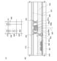
図1(E)に示すトランジスタ440は、ボトムゲート構造の一つであり逆スタガ型トラ
ンジスタともいうトランジスタの一例である。なお、図1は、トランジスタ440のチャ
ネル長方向の断面図である。1E is an example of a transistor having a bottom-gate structure and is also called an inverted staggered transistor. Note that FIG 1E is a cross-sectional view of the
図1(E)に示すように、トランジスタ440を含む半導体装置は、絶縁表面を有する基
板400上に、ゲート電極層401、ゲート絶縁膜402、酸化物半導体膜403、ソー
ス電極層405a、ドレイン電極層405bを有する。また、トランジスタ440を覆う
絶縁膜407が設けられている。1E, a semiconductor device including a
酸化物半導体膜403に用いる酸化物半導体としては、少なくともインジウム(In)を
含む。特にInと亜鉛(Zn)を含むことが好ましい。また、該酸化物半導体膜を用いた
トランジスタの電気特性のばらつきを減らすためのスタビライザーとして、それらに加え
てガリウム(Ga)を有することが好ましい。また、スタビライザーとしてスズ(Sn)
を有することが好ましい。また、スタビライザーとしてハフニウム(Hf)を有すること
が好ましい。また、スタビライザーとしてアルミニウム(Al)を有することが好ましい
。また、スタビライザーとしてジルコニウム(Zr)を有することが好ましい。The oxide semiconductor used for the
It is preferable that the stabilizer is hafnium (Hf). It is preferable that the stabilizer is aluminum (Al). It is preferable that the stabilizer is zirconium (Zr).
また、他のスタビライザーとして、ランタノイドである、ランタン(La)、セリウム(
Ce)、プラセオジム(Pr)、ネオジム(Nd)、サマリウム(Sm)、ユウロピウム
(Eu)、ガドリニウム(Gd)、テルビウム(Tb)、ジスプロシウム(Dy)、ホル
ミウム(Ho)、エルビウム(Er)、ツリウム(Tm)、イッテルビウム(Yb)、ル
テチウム(Lu)のいずれか一種あるいは複数種を有してもよい。Other stabilizers include lanthanides such as lanthanum (La) and cerium (
The element may have one or more of the following: arsenic (Ce), praseodymium (Pr), neodymium (Nd), samarium (Sm), europium (Eu), gadolinium (Gd), terbium (Tb), dysprosium (Dy), holmium (Ho), erbium (Er), thulium (Tm), ytterbium (Yb), and lutetium (Lu).
例えば、酸化物半導体として、酸化インジウム、酸化スズ、酸化亜鉛、In-Zn系酸化
物、In-Mg系酸化物、In-Ga系酸化物、In-Ga-Zn系酸化物(IGZOと
も表記する)、In-Al-Zn系酸化物、In-Sn-Zn系酸化物、In-Hf-Z
n系酸化物、In-La-Zn系酸化物、In-Ce-Zn系酸化物、In-Pr-Zn
系酸化物、In-Nd-Zn系酸化物、In-Sm-Zn系酸化物、In-Eu-Zn系
酸化物、In-Gd-Zn系酸化物、In-Tb-Zn系酸化物、In-Dy-Zn系酸
化物、In-Ho-Zn系酸化物、In-Er-Zn系酸化物、In-Tm-Zn系酸化
物、In-Yb-Zn系酸化物、In-Lu-Zn系酸化物、In-Sn-Ga-Zn系
酸化物、In-Hf-Ga-Zn系酸化物、In-Al-Ga-Zn系酸化物、In-S
n-Al-Zn系酸化物、In-Sn-Hf-Zn系酸化物、In-Hf-Al-Zn系
酸化物を用いることができる。Examples of oxide semiconductors include indium oxide, tin oxide, zinc oxide, In-Zn-based oxides, In-Mg-based oxides, In-Ga-based oxides, In-Ga-Zn-based oxides (also referred to as IGZO), In-Al-Zn-based oxides, In-Sn-Zn-based oxides, and In-Hf-Z.
n-based oxides, In-La-Zn-based oxides, In-Ce-Zn-based oxides, In-Pr-Zn
based oxides, In-Nd-Zn based oxides, In-Sm-Zn based oxides, In-Eu-Zn based oxides, In-Gd-Zn based oxides, In-Tb-Zn based oxides, In-Dy-Zn based oxides, In-Ho-Zn based oxides, In-Er-Zn based oxides, In-Tm-Zn based oxides, In-Yb-Zn based oxides, In-Lu-Zn based oxides, In-Sn-Ga-Zn based oxides, In-Hf-Ga-Zn based oxides, In-Al-Ga-Zn based oxides, In-S
Examples of the oxide that can be used include n-Al-Zn based oxides, In-Sn-Hf-Zn based oxides, and In-Hf-Al-Zn based oxides.
なお、ここで、例えば、In-Ga-Zn系酸化物とは、InとGaとZnを主成分とし
て有する酸化物という意味であり、InとGaとZnの比率は問わない。また、InとG
aとZn以外の金属元素が入っていてもよい。In addition, for example, an In-Ga-Zn oxide means an oxide having In, Ga, and Zn as main components, and the ratio of In, Ga, and Zn does not matter.
Metal elements other than a and Zn may be present.
また、酸化物半導体として、InMO3(ZnO)m(m>0、且つ、mは整数でない)
で表記される材料を用いてもよい。なお、Mは、Ga、Fe、Mn及びCoから選ばれた
一の金属元素または複数の金属元素を示す。また、酸化物半導体として、In2SnO5
(ZnO)n(n>0、且つ、nは整数)で表記される材料を用いてもよい。In addition, the oxide semiconductor may be InMO3 (ZnO)m (m>0, and m is not an integer).
In addition, M represents one or more metal elements selected from Ga, Fe, Mn, and Co. In addition, asthe oxidesemiconductor , a material represented by the formula:
A material expressed as (ZnO)n (n>0, and n is an integer) may be used.
例えば、In:Ga:Zn=1:1:1(=1/3:1/3:1/3)、In:Ga:Z
n=2:2:1(=2/5:2/5:1/5)、あるいはIn:Ga:Zn=3:1:2
(=1/2:1/6:1/3)の原子数比のIn-Ga-Zn系酸化物やその組成の近傍
の酸化物を用いることができる。あるいは、In:Sn:Zn=1:1:1(=1/3:
1/3:1/3)、In:Sn:Zn=2:1:3(=1/3:1/6:1/2)あるい
はIn:Sn:Zn=2:1:5(=1/4:1/8:5/8)の原子数比のIn-Sn
-Zn系酸化物やその組成の近傍の酸化物を用いるとよい。For example, In:Ga:Zn=1:1:1 (=1/3:1/3:1/3), In:Ga:Z
n=2:2:1 (=2/5:2/5:1/5), or In:Ga:Zn=3:1:2
In-Ga-Zn oxides having an atomic ratio of In:Sn:Zn=1:1:1 (=1/3:1/6:1/3) or oxides having a similar composition can be used.
In-Sn with an atomic ratio of In:Sn:Zn=2:1:3 (=1/3:1/3:1/6:1/2) or In:Sn:Zn=2:1:5 (=1/4:1/8:5/8)
It is preferable to use a -Zn-based oxide or an oxide having a composition close to that.
しかし、インジウムを含む酸化物半導体は、これらに限られず、必要とする電気特性(移
動度、しきい値、ばらつき等)に応じて適切な組成のものを用いればよい。また、必要と
する電気特性を得るために、キャリア濃度や不純物濃度、欠陥密度、金属元素と酸素の原
子数比、原子間距離、密度等を適切なものとすることが好ましい。However, the oxide semiconductor containing indium is not limited to these, and an oxide semiconductor having an appropriate composition may be used depending on required electrical characteristics (mobility, threshold, variation, etc.) In order to obtain required electrical characteristics, it is preferable to appropriately select the carrier concentration, impurity concentration, defect density, atomic ratio of metal element to oxygen, interatomic distance, density, and the like.
例えば、In-Sn-Zn系酸化物では比較的容易に高い移動度が得られる。しかしなが
ら、In-Ga-Zn系酸化物でも、バルク内欠陥密度を低くすることにより移動度を上
げることができる。For example, high mobility can be obtained relatively easily in In--Sn--Zn oxides, but mobility can also be increased in In--Ga--Zn oxides by lowering the bulk defect density.
なお、例えば、In、Ga、Znの原子数比がIn:Ga:Zn=a:b:c(a+b+
c=1)である酸化物の組成が、原子数比がIn:Ga:Zn=A:B:C(A+B+C
=1)の酸化物の組成の近傍であるとは、a、b、cが、(a-A)2+(b-B)2+
(c-C)2≦r2を満たすことをいう。rとしては、例えば、0.05とすればよい。
他の酸化物でも同様である。For example, the atomic ratio of In, Ga, and Zn is In:Ga:Zn=a:b:c (a+b+
The composition of the oxide in which the atomic ratio is In:Ga:Zn=A:B:C (A+B+C
= 1), a, b, and c are in the vicinity of the oxide composition (a-A)2 + (b-B)2 +
This means that (cC)2 ≦r2 is satisfied, where r is set to, for example, 0.05.
The same is true for other oxides.
酸化物半導体膜403は、単結晶、多結晶(ポリクリスタルともいう。)または非晶質な
どの状態をとる。The
好ましくは、酸化物半導体膜403は、CAAC-OS(C Axis Aligned
Crystalline Oxide Semiconductor)膜とする。The
The film is a crystalline oxide semiconductor film.
CAAC-OS膜は、完全な単結晶ではなく、完全な非晶質でもない。CAAC-OS膜
は、非晶質相に結晶部及び非晶質部を有する結晶-非晶質混相構造の酸化物半導体膜であ
る。なお、当該結晶部は、一辺が100nm未満の立方体内に収まる大きさであることが
多い。透過型電子顕微鏡(TEM:Transmission Electron Mi
croscope)による観察像では、CAAC-OS膜に含まれる非晶質部と結晶部と
の境界は必ずしも明確ではない。また、TEMによってCAAC-OS膜には粒界(グレ
インバウンダリーともいう。)は確認できない。そのため、CAAC-OS膜は、粒界に
起因する電子移動度の低下が抑制される。The CAAC-OS film is neither completely single crystalline nor completely amorphous. The CAAC-OS film is an oxide semiconductor film having a crystalline-amorphous mixed phase structure in which a crystalline part and an amorphous part are included in an amorphous phase. Note that the crystalline part is often within a cube with one side less than 100 nm.
In a cross-sectional image, the boundary between the amorphous and crystalline parts in the CAAC-OS film is not necessarily clear. Furthermore, no grain boundaries can be confirmed in the CAAC-OS film by TEM. Therefore, the decrease in electron mobility due to grain boundaries is suppressed in the CAAC-OS film.
CAAC-OS膜に含まれる結晶部は、c軸がCAAC-OS膜の被形成面の法線ベクト
ルまたは表面の法線ベクトルに平行な方向に揃い、かつab面に垂直な方向から見て三角
形状または六角形状の原子配列を有し、c軸に垂直な方向から見て金属原子が層状または
金属原子と酸素原子とが層状に配列している。なお、異なる結晶部間で、それぞれa軸及
びb軸の向きが異なっていてもよい。本明細書において、単に垂直と記載する場合、85
°以上95°以下の範囲も含まれることとする。また、単に平行と記載する場合、-5°
以上5°以下の範囲も含まれることとする。なお、酸化物半導体膜を構成する酸素の一部
は窒素で置換されてもよい。The crystal parts included in the CAAC-OS film have c-axes aligned in a direction parallel to the normal vector of the surface on which the CAAC-OS film is formed or the normal vector of the surface, and have a triangular or hexagonal atomic arrangement when viewed from a direction perpendicular to the a-b plane, with metal atoms arranged in layers or metal atoms and oxygen atoms arranged in layers when viewed from a direction perpendicular to the c-axis. Note that the directions of the a-axis and b-axis may differ between different crystal parts. In the present specification, when it is simply described as "perpendicular," the direction is 85
The range of -5° to 95° is also included.
The range also includes a range of more than or equal to 5°. Note that part of oxygen contained in the oxide semiconductor film may be substituted with nitrogen.
なお、CAAC-OS膜において、結晶部の分布が一様でなくてもよい。例えば、CAA
C-OS膜の形成過程において、酸化物半導体膜の表面側から結晶成長させる場合、被形
成面の近傍に対し表面の近傍では結晶部の占める割合が高くなることがある。また、CA
AC-OS膜へ不純物を添加することにより、当該不純物添加領域において結晶部が非晶
質化することもある。Note that the distribution of crystal parts in the CAAC-OS film does not have to be uniform.
In the process of forming a C-OS film, when crystals are grown from the surface side of the oxide semiconductor film, the proportion of crystal parts in the vicinity of the surface may be higher than that in the vicinity of the formation surface.
Adding an impurity to the AC-OS film may cause a crystalline portion in a region where the impurity has been added to become amorphous.
CAAC-OS膜に含まれる結晶部のc軸は、CAAC-OS膜の被形成面の法線ベクト
ルまたは表面の法線ベクトルに平行な方向に揃うため、CAAC-OS膜の形状(被形成
面の断面形状または表面の断面形状)によっては互いに異なる方向を向くことがある。な
お、結晶部のc軸の方向は、CAAC-OS膜が形成されたときの被形成面の法線ベクト
ルまたは表面の法線ベクトルに平行な方向となる。結晶部は、成膜することにより、また
は成膜後に加熱処理などの結晶化処理を行うことにより形成される。The c-axes of the crystal parts included in the CAAC-OS film are aligned in a direction parallel to the normal vector of the surface on which the CAAC-OS film is formed or the normal vector of the surface, and may be oriented in a different direction depending on the shape of the CAAC-OS film (the cross-sectional shape of the surface on which the CAAC-OS film is formed or the cross-sectional shape of the surface). Note that the c-axes of the crystal parts are oriented in a direction parallel to the normal vector of the surface on which the CAAC-OS film is formed or the normal vector of the surface when the CAAC-OS film is formed. The crystal parts are formed by film formation or by carrying out a crystallization treatment such as a heat treatment after film formation.
CAAC-OS膜を用いたトランジスタは、可視光や紫外光の照射による電気特性の変動
が小さい。よって、当該トランジスタは、信頼性が高い。A transistor including a CAAC-OS film has small changes in electrical characteristics due to irradiation with visible light or ultraviolet light, and thus has high reliability.
なお、酸化物半導体膜を構成する酸素の一部は窒素で置換されてもよい。Note that some of the oxygen constituting the oxide semiconductor film may be replaced with nitrogen.
また、CAAC-OS膜のように結晶部を有する酸化物半導体では、よりバルク内欠陥を
低減することができ、表面の平坦性を高めれば非晶質状態の酸化物半導体以上の移動度を
得ることができる。表面の平坦性を高めるためには、平坦な表面上に酸化物半導体を形成
することが好ましく、具体的には、平均面粗さ(Ra)が1nm以下、好ましくは0.3
nm以下、より好ましくは0.1nm以下の表面上に形成するとよい。In addition, in an oxide semiconductor having a crystalline part such as a CAAC-OS film, defects in the bulk can be further reduced, and mobility higher than that of an oxide semiconductor in an amorphous state can be obtained by improving the flatness of the surface. In order to improve the flatness of the surface, it is preferable to form an oxide semiconductor on a flat surface. Specifically, the average surface roughness (Ra) is 1 nm or less, preferably 0.3 nm or less.
It is preferable to form the surface on a thickness of 0.1 nm or less, and more preferably on a thickness of 0.1 nm or less.
なお、Raは、JIS B601:2001(ISO4287:1997)で定義されて
いる算術平均粗さを曲面に対して適用できるよう三次元に拡張したものであり、「基準面
から指定面までの偏差の絶対値を平均した値」と表現でき、以下の式にて定義される。Note that Ra is a three-dimensional extension of the arithmetic mean roughness defined in JIS B601:2001 (ISO 4287:1997) so that it can be applied to curved surfaces, and can be expressed as "the average of the absolute values of the deviations from a reference surface to a specified surface" and is defined by the following formula.
ここで、指定面とは、粗さ計測の対象となる面であり、座標((x1,y1,f(x1,
y1))(x1,y2,f(x1,y2))(x2,y1,f(x2,y1))(x2,
y2,f(x2,y2))の4点で表される四角形の領域とし、指定面をxy平面に投影
した長方形の面積をS0、基準面の高さ(指定面の平均の高さ)をZ0とする。Raは原
子間力顕微鏡(AFM:Atomic Force Microscope)にて測定可
能である。Here, the designated surface is a surface to be subjected to roughness measurement, and is represented by coordinates ((x1 ,y1 , f(x1 ,
y1 ))(x1 ,y2 ,f(x1 ,y2 ))(x2 ,y1 ,f(x2 ,y1 ))(x2 ,
The area ofa rectangle obtained by projectingthe specified surface onto the xy plane is S0, and the height of the reference plane (average height of the specified surface) isZ0 .Ra can be measured with an atomic force microscope (AFM).
また、基準面は、指定面の平均の高さにおける、XY平面と平行な面である。つまり、指
定面の高さの平均値をZ0とするとき、基準面の高さもZ0で表される。The reference plane is a plane parallel to the XY plane at the average height of the specified plane. In other words, when the average value of the height of the specified plane isZ0 , the height of the reference plane is also expressed asZ0 .
ただし、本実施の形態で説明するトランジスタ440は、ボトムゲート型であるため、酸
化物半導体膜の下方には基板400とゲート電極層401とゲート絶縁膜402が存在し
ている。従って、上記平坦な表面を得るためにゲート電極層401及びゲート絶縁膜40
2を形成した後、化学的機械的研磨(CMP:Chemical Mechanical
Polishing)処理などの平坦化処理を行ってもよい。However, since the
After forming the 2, chemical mechanical polishing (CMP) is performed.
A flattening process such as polishing may be performed.
酸化物半導体膜403の膜厚は、1nm以上30nm以下(好ましくは5nm以上10n
m以下)とし、スパッタリング法、MBE(Molecular Beam Epita
xy)法、CVD法、パルスレーザ堆積法、ALD(Atomic Layer Dep
osition)法等を適宜用いることができる。また、酸化物半導体膜403は、スパ
ッタリングターゲット表面に対し、概略垂直に複数の基板表面がセットされた状態で成膜
を行うスパッタリング装置を用いて成膜してもよい。The thickness of the
m or less), and sputtering method, MBE (Molecular Beam Epitaxy)
xy) method, CVD method, pulsed laser deposition method, ALD (Atomic Layer Depth
Alternatively, the
図1(A)乃至(E)にトランジスタ440を有する半導体装置の作製方法の一例を示す
。1A to 1E show an example of a method for manufacturing a semiconductor device including a
絶縁表面を有する基板400に使用することができる基板に大きな制限はないが、少なく
とも、後の熱処理に耐えうる程度の耐熱性を有していることが必要となる。例えば、バリ
ウムホウケイ酸ガラスやアルミノホウケイ酸ガラスなどのガラス基板、セラミック基板、
石英基板、サファイア基板などを用いることができる。また、シリコンや炭化シリコンな
どの単結晶半導体基板、多結晶半導体基板、シリコンゲルマニウムなどの化合物半導体基
板、SOI基板などを適用することもでき、これらの基板上に半導体素子が設けられたも
のを、基板400として用いてもよい。There is no particular limitation on the substrate that can be used for the
A quartz substrate, a sapphire substrate, or the like can be used. In addition, a single crystal semiconductor substrate such as silicon or silicon carbide, a polycrystalline semiconductor substrate, a compound semiconductor substrate such as silicon germanium, an SOI substrate, or the like can also be applied, and any of these substrates on which semiconductor elements are provided may be used as the
また、基板400として、可撓性基板を用いて半導体装置を作製してもよい。可撓性を有
する半導体装置を作製するには、可撓性基板上に酸化物半導体膜403を含むトランジス
タ440を直接作製してもよいし、他の作製基板に酸化物半導体膜403を含むトランジ
スタ440を作製し、その後可撓性基板に剥離、転置してもよい。なお、作製基板から可
撓性基板に剥離、転置するために、作製基板と酸化物半導体膜を含むトランジスタ440
との間に剥離層を設けるとよい。Alternatively, a semiconductor device may be manufactured using a flexible substrate as the
A release layer may be provided between the film and the substrate.
基板400上に下地膜として絶縁膜を設けてもよい。絶縁膜としては、プラズマCVD法
又はスパッタリング法等により、酸化シリコン、酸化窒化シリコン、酸化アルミニウム、
酸化窒化アルミニウム、酸化ハフニウム、酸化ガリウムなどの酸化物絶縁膜、窒化シリコ
ン、窒化酸化シリコン、窒化アルミニウム、窒化酸化アルミニウムなどの窒化物絶縁膜、
又はこれらの混合材料を用いて形成することができる。An insulating film may be provided as a base film over the
Oxide insulating films such as aluminum oxynitride, hafnium oxide, and gallium oxide; nitride insulating films such as silicon nitride, silicon nitride oxide, aluminum nitride, and aluminum nitride oxide;
Or, it may be formed using a mixture of these materials.
基板400(又は基板400及び絶縁膜)に加熱処理を行ってもよい。例えば、高温のガ
スを用いて加熱処理を行うGRTA(Gas Rapid Thermal Annea
l)装置により、650℃、1分~5分間、加熱処理を行えばよい。なお、GRTAにお
ける高温のガスには、アルゴンなどの希ガス、または窒素のような、加熱処理によって被
処理物と反応しない不活性気体が用いられる。また、電気炉により、500℃、30分~
1時間、加熱処理を行ってもよい。Heat treatment may be performed on the substrate 400 (or the
Heat treatment may be performed at 650° C. for 1 to 5 minutes in a GRTA apparatus. Note that the high-temperature gas used in the GRTA is an inert gas such as a rare gas, such as argon, or nitrogen, which does not react with the object to be treated by heat treatment. Alternatively, heat treatment may be performed at 500° C. for 30 to 5 minutes in an electric furnace.
Heat treatment may be carried out for 1 hour.
次に基板400上に導電膜を形成し、該導電膜をエッチングすることで、ゲート電極層4
01を形成する。導電膜のエッチングは、ドライエッチングでもウェットエッチングでも
よく、両方を用いてもよい。Next, a conductive film is formed over the
The conductive film may be etched by dry etching or wet etching, or may be etched by both.
ゲート電極層401の材料は、モリブデン、チタン、タンタル、タングステン、アルミニ
ウム、銅、クロム、ネオジム、スカンジウム等の金属材料またはこれらを主成分とする合
金材料を用いて形成することができる。また、ゲート電極層401としてリン等の不純物
元素をドーピングした多結晶シリコン膜に代表される半導体膜、ニッケルシリサイドなど
のシリサイド膜を用いてもよい。ゲート電極層401は、単層構造としてもよいし、積層
構造としてもよい。The
また、ゲート電極層401の材料は、酸化タングステンを含むインジウム酸化物、酸化チ
タンを含むインジウム酸化物、インジウムスズ酸化物、酸化チタンを含むインジウムスズ
酸化物、酸化ケイ素を添加したインジウムスズ酸化物、インジウム亜鉛酸化物、酸化タン
グステンを含むインジウム亜鉛酸化物、などの導電性材料を適用することもできる。また
、上記導電性材料と、上記金属材料の積層構造とすることもできる。The
また、ゲート絶縁膜402と接するゲート電極層401として、窒素を含む金属酸化物、
具体的には、窒素を含むIn-Ga-Zn系酸化物膜や、窒素を含むIn-Sn系酸化物
膜や、窒素を含むIn-Ga系酸化物膜や、窒素を含むIn-Zn系酸化物膜や、窒素を
含む酸化スズ膜や、窒素を含む酸化インジウム膜や、金属窒化物膜(InN、SnNなど
)を用いることができる。これらの膜は5eV(電子ボルト)、好ましくは5.5eV(
電子ボルト)以上の仕事関数を有し、ゲート電極層として用いた場合、トランジスタの電
気特性のしきい値電圧をプラスにすることができる。The
Specifically, an In-Ga-Zn oxide film containing nitrogen, an In-Sn oxide film containing nitrogen, an In-Ga oxide film containing nitrogen, an In-Zn oxide film containing nitrogen, a tin oxide film containing nitrogen, an indium oxide film containing nitrogen, or a metal nitride film (InN, SnN, etc.) can be used. These films have a potential of 5 eV (electron volts), preferably 5.5 eV (
When a gate electrode layer is formed using such a material, the threshold voltage of the transistor can be made positive.
本実施の形態では、スパッタリング法により膜厚100nmのタングステン膜を形成する
。In this embodiment mode, a tungsten film is formed to a thickness of 100 nm by sputtering.
また、ゲート電極層401形成後に、基板400、及びゲート電極層401に加熱処理を
行ってもよい。例えば、GRTA装置により、650℃、1分~5分間、加熱処理を行え
ばよい。また、電気炉により、500℃、30分~1時間、加熱処理を行ってもよい。After the
次いで、ゲート電極層401上にゲート絶縁膜402を形成する。Next, a
なお、ゲート絶縁膜402の被覆性を向上させるために、ゲート電極層401表面に平坦
化処理を行ってもよい。特にゲート絶縁膜402として膜厚の薄い絶縁膜を用いる場合、
ゲート電極層401表面の平坦性が良好であることが好ましい。Note that planarization treatment may be performed on the surface of the
It is preferable that the surface of the
ゲート絶縁膜402の膜厚は、1nm以上20nm以下とし、スパッタリング法、MBE
法、CVD法、パルスレーザ堆積法、ALD法等を適宜用いることができる。また、ゲー
ト絶縁膜402は、スパッタリングターゲット表面に対し、概略垂直に複数の基板表面が
セットされた状態で成膜を行うスパッタリング装置を用いて成膜してもよい。The thickness of the
A deposition method, a CVD method, a pulsed laser deposition method, an ALD method, or the like can be appropriately used. The
ゲート絶縁膜402の材料としては、酸化シリコン膜、酸化ガリウム膜、酸化アルミニウ
ム膜、窒化シリコン膜、酸化窒化シリコン膜、酸化窒化アルミニウム膜、または窒化酸化
シリコン膜を用いて形成することができる。The
また、ゲート絶縁膜402の材料として酸化ハフニウム、酸化イットリウム、ハフニウム
シリケート(HfSixOy(x>0、y>0))、窒素が添加されたハフニウムシリケ
ート(HfSiOxNy(x>0、y>0))、ハフニウムアルミネート(HfAlxO
y(x>0、y>0))、酸化ランタンなどのhigh-k材料を用いることでゲートリ
ーク電流を低減できる。さらに、ゲート絶縁膜402は、単層構造としても良いし、積層
構造としても良い。The material of the
A gate leakage current can be reduced by using a high-k material such as lanthanum oxide or a silicide( x>0, y>0) ...
ゲート絶縁膜402は、酸化物半導体膜403と接する部分において酸素を含むことが好
ましい。特に、ゲート絶縁膜402は、膜中(バルク中)に少なくとも化学量論的組成に
おける含有量を超える量の酸素が存在することが好ましく、例えば、ゲート絶縁膜402
として、酸化シリコン膜を用いる場合には、SiO2+α(ただし、α>0)とする。The
When a silicon oxide film is used, the formula is SiO2 +α (where α>0).
酸素の供給源となる、酸素を多く(過剰に)含むゲート絶縁膜402を酸化物半導体膜4
03と接して設けることによって、該ゲート絶縁膜402から酸化物半導体膜403へ酸
素を供給することができる。酸化物半導体膜403及びゲート絶縁膜402を少なくとも
一部が接した状態で加熱処理を行うことによって酸化物半導体膜403への酸素の供給を
行ってもよい。The
By providing the
酸化物半導体膜403へ酸素を供給することにより、膜中の酸素欠損を補填することがで
きる。さらに、ゲート絶縁膜402は、作製するトランジスタのサイズやゲート絶縁膜4
02の段差被覆性を考慮して形成することが好ましい。By supplying oxygen to the
It is preferable to form the film 02 taking into consideration the step coverage.
本実施の形態では、高密度プラズマCVD法により膜厚200nmの酸化窒化シリコン膜
を形成する。In this embodiment mode, a silicon oxynitride film is formed to a thickness of 200 nm by high density plasma CVD.
また、ゲート絶縁膜402形成後に、基板400、ゲート電極層401、及びゲート絶縁
膜402に加熱処理を行ってもよい。例えば、GRTA装置により、650℃、1分~5
分間、加熱処理を行えばよい。また、電気炉により、500℃、30分~1時間、加熱処
理を行ってもよい。After the
Alternatively, the heat treatment may be performed in an electric furnace at 500° C. for 30 minutes to 1 hour.
次に、ゲート絶縁膜402上に酸化物半導体膜403を形成する(図1(A)参照)。Next, an
酸化物半導体膜403の形成工程において、酸化物半導体膜403に水素、又は水がなる
べく含まれないようにするために、酸化物半導体膜403の成膜の前処理として、スパッ
タリング装置の予備加熱室でゲート絶縁膜402が形成された基板を予備加熱し、基板及
びゲート絶縁膜402に吸着した水素、水分などの不純物を脱離し排気することが好まし
い。なお、予備加熱室に設ける排気手段はクライオポンプが好ましい。In order to minimize the amount of hydrogen or water contained in the
ゲート絶縁膜402において酸化物半導体膜403が接して形成される領域に、平坦化処
理を行ってもよい。平坦化処理としては、特に限定されないが、研磨処理(例えば、CM
P処理)、ドライエッチング処理、プラズマ処理を用いることができる。A region of the
For example, a dry etching process, a plasma process, or the like can be used.
プラズマ処理としては、例えば、アルゴンガスを導入してプラズマを発生させる逆スパッ
タリングを行うことができる。逆スパッタリングとは、アルゴン雰囲気下で基板側にRF
電源を用いて電圧を印加して基板近傍にプラズマを形成して表面を改質する方法である。
なお、アルゴン雰囲気に代えて窒素、ヘリウム、酸素などを用いてもよい。逆スパッタリ
ングを行うと、ゲート絶縁膜402の表面に付着している粉状物質(パーティクル、ごみ
ともいう)を除去することができる。As the plasma treatment, for example, reverse sputtering can be performed by introducing argon gas to generate plasma. In reverse sputtering, RF is applied to the substrate side in an argon atmosphere.
This method involves applying voltage using a power supply to generate plasma in the vicinity of the substrate to modify the surface.
Note that the argon atmosphere may be replaced with nitrogen, helium, oxygen, or the like. By performing reverse sputtering, powdery substances (also referred to as particles or dust) attached to the surface of the
平坦化処理として、研磨処理、ドライエッチング処理、プラズマ処理は複数回行ってもよ
く、それらを組み合わせて行ってもよい。また、組み合わせて行う場合、工程順も特に限
定されず、ゲート絶縁膜402表面の凹凸状態に合わせて適宜設定すればよい。As the planarization treatment, a polishing treatment, a dry etching treatment, or a plasma treatment may be performed multiple times, or a combination of these may be performed. In addition, when a combination of these treatments is performed, the order of the steps is not particularly limited and may be appropriately set according to the unevenness of the surface of the
なお、酸化物半導体膜403は、成膜時に酸素が多く含まれるような条件(例えば、酸素
100%の雰囲気下でスパッタリング法により成膜を行うなど)で成膜して、酸素を多く
含む(好ましくは酸化物半導体が結晶状態における化学量論的組成に対し、酸素の含有量
が過剰な領域が含まれている)膜とすることが好ましい。Note that the
なお、本実施の形態において、酸化物半導体膜403として、AC電源装置を有するスパ
ッタリング装置を用いたスパッタリング法を用い、膜厚35nmのIn-Ga-Zn系酸
化物膜(IGZO膜)を成膜する。本実施の形態において、In:Ga:Zn=1:1:
1(=1/3:1/3:1/3)の原子比のIn-Ga-Zn系酸化物ターゲットを用い
る。なお、成膜条件は、酸素及びアルゴン雰囲気下(酸素流量比率50%)、圧力0.6
Pa、電源電力5kW、基板温度170℃とする。この成膜条件での成膜速度は、16n
m/minである。In this embodiment, a 35-nm-thick In—Ga—Zn-based oxide film (IGZO film) is formed as the
An In-Ga-Zn oxide target having an atomic ratio of 1/3:1/3:1/3 is used. The deposition conditions are an oxygen and argon atmosphere (oxygen flow rate ratio 50%), a pressure of 0.6, and a deposition temperature of 100° C.
The deposition conditions are: pressure, pressure drop, power supply power, and substrate temperature, 170° C. The deposition rate under these deposition conditions is 16n
m/min.
酸化物半導体膜403を、成膜する際に用いるスパッタリングガスは水素、水、水酸基又
は水素化物などの不純物が除去された高純度ガスを用いることが好ましい。It is preferable that a high-purity gas from which impurities such as hydrogen, water, a hydroxyl group, or hydride are removed be used as a sputtering gas used in forming the
減圧状態に保持された成膜室内に基板を保持する。そして、成膜室内の残留水分を除去し
つつ水素及び水分が除去されたスパッタリングガスを導入し、上記ターゲットを用いて基
板400上に酸化物半導体膜403を成膜する。成膜室内の残留水分を除去するためには
、吸着型の真空ポンプ、例えば、クライオポンプ、イオンポンプ、チタンサブリメーショ
ンポンプを用いることが好ましい。また、排気手段としては、ターボ分子ポンプにコール
ドトラップを加えたものであってもよい。クライオポンプを用いて排気した成膜室は、例
えば、水素原子、水(H2O)など水素原子を含む化合物(より好ましくは炭素原子を含
む化合物も)等が排気されるため、当該成膜室で成膜した酸化物半導体膜403に含まれ
る不純物の濃度を低減できる。The substrate is held in a deposition chamber maintained in a reduced pressure state. Then, a sputtering gas from which hydrogen and moisture have been removed is introduced while removing residual moisture in the deposition chamber, and the
また、ゲート絶縁膜402を大気に解放せずにゲート絶縁膜402と酸化物半導体膜40
3を連続的に形成することが好ましい。ゲート絶縁膜402を大気に曝露せずにゲート絶
縁膜402と酸化物半導体膜403を連続して形成すると、ゲート絶縁膜402表面に水
素や水分などの不純物が吸着することを防止することができる。In addition, the
When the
酸化物半導体膜403は、膜状の酸化物半導体膜をフォトリソグラフィ工程により島状の
酸化物半導体膜に加工して形成することができる。The
また、島状の酸化物半導体膜403を形成するためのレジストマスクをインクジェット法
で形成してもよい。レジストマスクをインクジェット法で形成するとフォトマスクを使用
しないため、製造コストを低減できる。Alternatively, a resist mask for forming the island-shaped
なお、酸化物半導体膜のエッチングは、ドライエッチングでもウェットエッチングでもよ
く、両方を用いてもよい。例えば、酸化物半導体膜のウェットエッチングに用いるエッチ
ング液としては、燐酸と酢酸と硝酸を混ぜた溶液などを用いることができる。また、IT
O-07N(関東化学社製)を用いてもよい。また、ICP(Inductively
Coupled Plasma:誘導結合型プラズマ)エッチング法によるドライエッチ
ングによってエッチング加工してもよい。The oxide semiconductor film may be etched by dry etching or wet etching, or may be etched by both. For example, a mixed solution of phosphoric acid, acetic acid, and nitric acid may be used as an etching solution for wet etching of the oxide semiconductor film.
O-07N (manufactured by Kanto Chemical Co., Ltd.) may also be used.
Alternatively, the etching may be performed by dry etching using an inductively coupled plasma (ICP) etching method.
また、酸化物半導体膜403に、過剰な水素(水や水酸基を含む)を除去(脱水化または
脱水素化)するための加熱処理を行ってもよい。加熱処理の温度は、300℃以上700
℃以下、または基板の歪み点未満とする。加熱処理は減圧下又は窒素雰囲気下などで行う
ことができる。Further, the
The temperature is set to be equal to or lower than the distortion point of the substrate. The heat treatment can be performed under reduced pressure or in a nitrogen atmosphere.
また、酸化物半導体膜403として結晶性酸化物半導体膜を用いる場合、結晶化のための
加熱処理を行ってもよい。In the case where a crystalline oxide semiconductor film is used as the
本実施の形態では、加熱処理装置の一つである電気炉に基板を導入し、酸化物半導体膜4
03に対して窒素雰囲気下450℃において1時間、さらに窒素及び酸素を含む雰囲気下
450℃において1時間の加熱処理を行う。In this embodiment, the substrate is placed in an electric furnace, which is a type of heat treatment device, and the oxide semiconductor film 4
Sample No. 03 is subjected to a heat treatment at 450° C. for 1 hour in a nitrogen atmosphere, and further to a heat treatment at 450° C. for 1 hour in an atmosphere containing nitrogen and oxygen.
なお、加熱処理装置は電気炉に限られず、抵抗発熱体などの発熱体からの熱伝導または熱
輻射によって、被処理物を加熱する装置を用いてもよい。例えば、GRTA装置、LRT
A(Lamp Rapid Thermal Anneal)装置等のRTA(Rapi
d Thermal Anneal)装置を用いることができる。LRTA装置は、ハロ
ゲンランプ、メタルハライドランプ、キセノンアークランプ、カーボンアークランプ、高
圧ナトリウムランプ、高圧水銀ランプなどのランプから発する光(電磁波)の輻射により
、被処理物を加熱する装置である。GRTA装置は、高温のガスを用いて加熱処理を行う
装置である。高温のガスには、アルゴンなどの希ガス、または窒素のような、加熱処理に
よって被処理物と反応しない不活性気体が用いられる。The heat treatment device is not limited to an electric furnace, and may be a device that heats the workpiece by heat conduction or heat radiation from a heating element such as a resistance heating element. For example, a GRTA device, an LRT device, etc.
RTA (Rapid Thermal Anneal) equipment such as
A LRTA (Low Reflow Thermal Anneal) apparatus can be used. The LRTA apparatus is an apparatus that heats the workpiece by radiating light (electromagnetic waves) emitted from a lamp such as a halogen lamp, a metal halide lamp, a xenon arc lamp, a carbon arc lamp, a high-pressure sodium lamp, or a high-pressure mercury lamp. The GRTA apparatus is an apparatus that performs heat treatment using a high-temperature gas. For the high-temperature gas, a rare gas such as argon or an inert gas such as nitrogen that does not react with the workpiece during heat treatment is used.
例えば、加熱処理として、650℃~700℃の高温に加熱した不活性ガス中に基板を入
れ、数分間加熱した後、基板を不活性ガス中から出すGRTAを行ってもよい。For example, as the heat treatment, GRTA may be performed in which the substrate is placed in an inert gas heated to a high temperature of 650° C. to 700° C., heated for several minutes, and then removed from the inert gas.
なお、加熱処理においては、窒素、またはヘリウム、ネオン、アルゴン等の希ガスに、水
、水素などが含まれないことが好ましい。または、熱処理装置に導入する窒素、またはヘ
リウム、ネオン、アルゴン等の希ガスの純度を、6N(99.9999%)以上好ましく
は7N(99.99999%)以上(即ち不純物濃度を1ppm以下、好ましくは0.1
ppm以下)とすることが好ましい。In the heat treatment, it is preferable that nitrogen or a rare gas such as helium, neon, or argon does not contain water, hydrogen, or the like. Alternatively, the purity of nitrogen or a rare gas such as helium, neon, or argon introduced into the heat treatment apparatus is 6N (99.9999%) or more, preferably 7N (99.99999%) or more (i.e., the impurity concentration is 1 ppm or less, preferably 0.1 ppm or less).
It is preferable that the content be less than or equal to 1 ppm.
また、加熱処理で酸化物半導体膜403を加熱した後、同じ炉に高純度の酸素ガス、高純
度の一酸化二窒素ガス、又は超乾燥エア(CRDS(キャビティリングダウンレーザー分
光法)方式の露点計を用いて測定した場合の水分量が20ppm(露点換算で-55℃)
以下、好ましくは1ppm以下、より好ましくは10ppb以下の空気)を導入してもよ
い。酸素ガスまたは一酸化二窒素ガスに、水、水素などが含まれないことが好ましい。ま
たは、熱処理装置に導入する酸素ガスまたは一酸化二窒素ガスの純度を、6N以上好まし
くは7N以上(即ち、酸素ガスまたは一酸化二窒素ガス中の不純物濃度を1ppm以下、
好ましくは0.1ppm以下)とすることが好ましい。酸素ガス又は一酸化二窒素ガスの
作用により、脱水化または脱水素化処理による不純物の排除工程によって同時に減少して
しまった酸化物半導体を構成する主成分材料である酸素を供給することによって、酸化物
半導体膜403を高純度化及びI型(真性)化することができる。After the
It is preferable that the oxygen gas or nitrous oxide gas does not contain water, hydrogen, etc. Alternatively, the purity of the oxygen gas or nitrous oxide gas introduced into the heat treatment device is 6N or more, preferably 7N or more (i.e., the impurity concentration in the oxygen gas or nitrous oxide gas is 1 ppm or less,
The concentration of oxygen in the
なお、脱水化又は脱水素化のための加熱処理を行うタイミングは、膜状の酸化物半導体膜
の形成後でも、島状の酸化物半導体膜403形成後でもよい。Note that the heat treatment for dehydration or dehydrogenation may be performed after the formation of the oxide semiconductor film or after the formation of the island-shaped
また、脱水化又は脱水素化のための加熱処理は、複数回行ってもよく、他の加熱処理と兼
ねてもよい。The heat treatment for dehydration or dehydrogenation may be performed multiple times, or may be performed together with other heat treatments.
脱水化又は脱水素化のための加熱処理を、酸化物半導体膜403として島状に加工される
前、膜状の酸化物半導体膜がゲート絶縁膜402を覆った状態で行うと、ゲート絶縁膜4
02に含まれる酸素が加熱処理によって放出されるのを防止することができるため好まし
い。When the heat treatment for dehydration or dehydrogenation is performed in a state where the oxide semiconductor film covers the
This is preferable because it is possible to prevent the oxygen contained in 02 from being released by the heat treatment.
また、脱水化又は脱水素化処理を行った酸化物半導体膜403に、酸素(少なくとも、酸
素ラジカル、酸素原子、酸素イオン、のいずれかを含む)を導入して膜中に酸素を供給し
てもよい。Further, oxygen (including at least any of oxygen radicals, oxygen atoms, and oxygen ions) may be introduced into the
また、脱水化又は脱水素化処理によって、酸化物半導体を構成する主成分材料である酸素
が同時に脱離して減少してしまうおそれがある。酸化物半導体膜において、酸素が脱離し
た箇所では酸素欠損が存在し、該酸素欠損に起因してトランジスタの電気的特性変動を招
くドナー準位が生じてしまう。In addition, oxygen, which is a main component material of the oxide semiconductor, may be simultaneously released and reduced by the dehydration or dehydrogenation treatment. In the oxide semiconductor film, oxygen vacancies are present in the portions from which oxygen is released, and the oxygen vacancies cause donor levels that cause fluctuations in the electrical characteristics of a transistor.
よって、脱水化又は脱水素化処理を行った酸化物半導体膜に、酸素(少なくとも、酸素ラ
ジカル、酸素原子、酸素イオン、のいずれかを含む)を供給することが好ましい。酸化物
半導体膜へ酸素を供給することにより、膜中の酸素欠損を補填することができる。Therefore, oxygen (including at least any of oxygen radicals, oxygen atoms, and oxygen ions) is preferably supplied to the oxide semiconductor film that has been subjected to dehydration or dehydrogenation treatment. By supplying oxygen to the oxide semiconductor film, oxygen vacancies in the film can be filled.
脱水化又は脱水素化処理を行った酸化物半導体膜403に、酸素を導入して膜中に酸素を
供給することによって、酸化物半導体膜403を高純度化、及びi型(真性)化すること
ができる。高純度化し、i型(真性)化した酸化物半導体膜403を有するトランジスタ
は、電気特性変動が抑制されており、電気的に安定である。By introducing oxygen into the
酸素の導入方法としては、イオン注入法、イオンドーピング法、プラズマイマージョンイ
オンインプランテーション法、プラズマ処理などを用いることができる。The oxygen can be introduced by ion implantation, ion doping, plasma immersion ion implantation, plasma treatment, or the like.
酸素の導入工程は、酸化物半導体膜403に酸素導入する場合、酸化物半導体膜403に
直接導入してもよいし、絶縁膜407などの他の膜を通過して酸化物半導体膜403へ導
入してもよい。酸素を他の膜を通過して導入する場合は、イオン注入法、イオンドーピン
グ法、プラズマイマージョンイオンインプランテーション法などを用いればよいが、酸素
を露出された酸化物半導体膜403へ直接導入する場合は、プラズマ処理なども用いるこ
とができる。In the step of introducing oxygen into the
酸化物半導体膜403への酸素の導入は、脱水化又は脱水素化処理を行った後が好ましい
が、特に限定されない。また、上記脱水化又は脱水素化処理を行った酸化物半導体膜40
3への酸素の導入は複数回行ってもよい。Oxygen is preferably introduced into the
The introduction of oxygen into 3 may be carried out multiple times.
好ましくはトランジスタに設けられる酸化物半導体膜は、酸化物半導体が結晶状態におけ
る化学量論的組成に対し、酸素の含有量が過剰な領域が含まれている膜とするとよい。こ
の場合、酸素の含有量は、酸化物半導体の化学量論的組成を超える程度とする。あるいは
、酸素の含有量は、単結晶の場合の酸素の量を超える程度とする。酸化物半導体の格子間
に酸素が存在する場合もある。Preferably, the oxide semiconductor film provided in the transistor includes a region in which the oxygen content is excessive with respect to the stoichiometric composition of the oxide semiconductor in a crystalline state. In this case, the oxygen content is set to be higher than the stoichiometric composition of the oxide semiconductor. Alternatively, the oxygen content is set to be higher than the amount of oxygen in the case of a single crystal. Oxygen may be present between lattices of the oxide semiconductor.
水素若しくは水分を酸化物半導体から除去し、不純物が極力含まれないように高純度化し
、酸素を供給して酸素欠損を補填することによりi型(真性)の酸化物半導体、又はi型
(真性)に限りなく近い酸化物半導体とすることができる。そうすることにより、酸化物
半導体のフェルミ準位(Ef)を真性フェルミ準位(Ei)と同じレベルにまですること
ができる。よって、該酸化物半導体膜をトランジスタに用いることで、酸素欠損に起因す
るトランジスタのしきい値電圧Vthのばらつき、しきい値電圧のシフトΔVthを低減
することができる。By removing hydrogen or moisture from the oxide semiconductor, purifying the oxide semiconductor so that impurities are contained as little as possible, and filling oxygen vacancies by supplying oxygen, an i-type (intrinsic) oxide semiconductor or an oxide semiconductor that is as close to i-type (intrinsic) as possible can be obtained. In this way, the Fermi level (Ef) of the oxide semiconductor can be made to be the same as the intrinsic Fermi level (Ei). Therefore, by using the oxide semiconductor film for a transistor, variations in the threshold voltage Vth of the transistor caused by oxygen vacancies and a threshold voltage shift ΔVth can be reduced.
次いで、ゲート電極層401、ゲート絶縁膜402、及び酸化物半導体膜403上に、ソ
ース電極層及びドレイン電極層(これと同じ層で形成される配線を含む)となる導電膜4
45を形成する(図1(B)参照)。Next, a conductive film 404 to be a source electrode layer and a drain electrode layer (including wirings formed in the same layer) is formed over the
45 is formed (see FIG. 1(B)).
導電膜445は後の加熱処理に耐えられる材料を用いる。ソース電極層、及びドレイン電
極層に用いる導電膜445としては、例えば、Al、Cr、Cu、Ta、Ti、Mo、W
から選ばれた元素を含む金属膜、または上述した元素を成分とする金属窒化物膜(窒化チ
タン膜、窒化モリブデン膜、窒化タングステン膜)等を用いることができる。また、Al
、Cuなどの金属膜の下側又は上側の一方または双方にTi、Mo、Wなどの高融点金属
膜またはそれらの金属窒化物膜(窒化チタン膜、窒化モリブデン膜、窒化タングステン膜
)を積層させた構成としても良い。また、ソース電極層、及びドレイン電極層に用いる導
電膜445としては、導電性の金属酸化物で形成しても良い。導電性の金属酸化物として
は酸化インジウム(In2O3)、酸化スズ(SnO2)、酸化亜鉛(ZnO)、インジ
ウムスズ酸化物(In2O3―SnO2、ITOと略記する)、インジウム亜鉛酸化物(
In2O3―ZnO)またはこれらの金属酸化物材料に酸化シリコンを含ませたものを用
いることができる。The
Metal films containing an element selected from the above, or metal nitride films containing the above elements (titanium nitride film, molybdenum nitride film, tungsten nitride film), etc. can be used.
A high melting point metal film such as Ti, Mo, or W or a metal nitride film of such a metal (titanium nitride film, molybdenum nitride film, or tungsten nitride film) may be stacked on one or both of the upper and lower sides of a metal film such as Cu. The
In2 O3 —ZnO) or these metal oxide materials containing silicon oxide can be used.
フォトリソグラフィ工程により導電膜445上にレジストマスク448a、448bを形
成し、ハロゲンを含むガス447を用いた選択的なエッチングを行ってソース電極層40
5a、ドレイン電極層405bを形成する(図1(C)参照)。ソース電極層405a、
ドレイン電極層405bを形成した後、レジストマスク448a、448bを除去する。Resist
5a, the
After the
レジストマスク448a、448b形成時の露光には、紫外線やKrFレーザ光やArF
レーザ光を用いるとよい。酸化物半導体膜403上で隣り合うソース電極層405aの下
端部とドレイン電極層405bの下端部との間隔幅によって後に形成されるトランジスタ
440のチャネル長Lが決定される。なお、チャネル長L=25nm未満の露光を行う場
合には、数nm~数10nmと極めて波長が短い超紫外線(Extreme Ultra
violet)を用いてレジストマスク448a、448b形成時の露光を行うとよい。
超紫外線による露光は、解像度が高く焦点深度も大きい。従って、後に形成されるトラン
ジスタのチャネル長Lを10nm以上1000nm以下とすることも可能であり、回路の
動作速度を高速化できる。The resist
Laser light is preferably used. A channel length L of a
It is preferable to use a light-exposure mask such as fluorene or violet for exposure when forming the resist
Exposure to extreme ultraviolet light has high resolution and a large depth of focus, so that the channel length L of a transistor to be formed later can be set to 10 nm or more and 1000 nm or less, thereby increasing the operating speed of the circuit.
また、フォトリソグラフィ工程で用いるフォトマスク数及び工程数を削減するため、透過
した光が複数の強度となる露光マスクである多階調マスクによって形成されたレジストマ
スクを用いてエッチング工程を行ってもよい。多階調マスクを用いて形成したレジストマ
スクは複数の膜厚を有する形状となり、エッチングを行うことでさらに形状を変形するこ
とができるため、異なるパターンに加工する複数のエッチング工程に用いることができる
。よって、一枚の多階調マスクによって、少なくとも二種類以上の異なるパターンに対応
するレジストマスクを形成することができる。よってフォトマスク数を削減することがで
き、対応するフォトリソグラフィ工程も削減できるため、工程の簡略化が可能となる。In addition, in order to reduce the number of photomasks and steps used in the photolithography process, the etching process may be performed using a resist mask formed by a multi-tone mask, which is an exposure mask that transmits light with multiple intensities. The resist mask formed using the multi-tone mask has a shape with multiple film thicknesses, and the shape can be further deformed by etching, so that it can be used in multiple etching steps to process into different patterns. Therefore, a single multi-tone mask can form resist masks corresponding to at least two or more different patterns. Therefore, the number of photomasks can be reduced, and the corresponding photolithography steps can also be reduced, making it possible to simplify the process.
本実施の形態では、導電膜445のエッチングには、ハロゲンを含むガス447を用いる
。ハロゲンを含むガス447としては、塩素を含むガス、例えば、塩素(Cl2)、三塩
化ホウ素(BCl3)、四塩化ケイ素(SiCl4)、四塩化炭素(CCl4)などを含
むガスを用いることができる。また、ハロゲンを含むガス447として、フッ素を含むガ
ス、例えば、四フッ化炭素(CF4)、フッ化硫黄(SF6)、フッ化窒素(NF3)、
トリフルオロメタン(CHF3)などを含むガスを用いることができる。また、これらの
ガスにヘリウム(He)やアルゴン(Ar)などの希ガスを添加したガス、などを用いる
ことができる。In this embodiment, a
A gas containing trifluoromethane (CHF3 ) or the like can be used. In addition, a gas containing these gases to which a rare gas such as helium (He) or argon (Ar) has been added can also be used.
エッチング法としては、平行平板型RIE(Reactive Ion Etching
)法や、ICPエッチング法を用いることができる。所望の加工形状にエッチングできる
ように、エッチング条件(コイル型の電極に印加される電力量、基板側の電極に印加され
る電力量、基板側の電極温度等)を適宜調節する。The etching method is parallel plate type RIE (Reactive Ion Etching).
In order to obtain a desired processed shape, the etching conditions (such as the amount of power applied to the coil-shaped electrode, the amount of power applied to the electrode on the substrate side, and the temperature of the electrode on the substrate side) are appropriately adjusted.
本実施の形態では、導電膜445としてスパッタリング法により膜厚100nmのチタン
膜、膜厚400nmのアルミニウム膜、膜厚100nmのチタン膜の積層を用いる。導電
膜445のエッチングは、ドライエッチング法により、チタン膜、アルミニウム膜、チタ
ン膜の積層をエッチングすることで、ソース電極層405a、ドレイン電極層405bを
形成する。In this embodiment mode, a stack of a 100-nm-thick titanium film, a 400-nm-thick aluminum film, and a 100-nm-thick titanium film is formed by a sputtering method as the
本実施の形態では、第1のエッチング条件でチタン膜とアルミニウム膜の2層をエッチン
グした後、第2のエッチング条件で残りのチタン膜単層を除去する。なお、第1のエッチ
ング条件は、エッチングガス(BCl3:Cl2=750sccm:150sccm)を
用い、バイアス電力を1500Wとし、ICP電源電力を0Wとし、圧力を2.0Paと
する。第2のエッチング条件は、エッチングガス(BCl3:Cl2=700sccm:
100sccm)を用い、バイアス電力を750Wとし、ICP電源電力を0Wとし、圧
力を2.0Paとする。In this embodiment, the two layers of titanium and aluminum are etched under the first etching condition, and then the remaining titanium single layer is removed under the second etching condition. The first etching condition is to use an etching gas (BCl3 :Cl2 =750sccm:150sccm), a bias power of 1500W, an ICP power supply power of 0W, and a pressure of 2.0Pa. The second etching condition is to use an etching gas (BCl3 :Cl2 =700sccm:
100 sccm), bias power is 750 W, ICP power supply power is 0 W, and pressure is 2.0 Pa.
ソース電極層405a及びドレイン電極層405bを形成するエッチング工程において、
酸化物半導体膜表面及び該近傍に、エッチング材(エッチングガス、又はエッチング溶液
)による残留物が生じてしまう。このような残留物は、リーク電流などトランジスタの電
気特性の低下や変動を招く要因となる。また、エッチング材に含まれる元素が酸化物半導
体膜403中に混入、又は付着し、トランジスタ特性に悪影響を与える恐れがある。In the etching process for forming the
Residues of the etching material (etching gas or etching solution) are generated on the surface of the oxide semiconductor film and in the vicinity thereof. Such residues may cause deterioration or variation in the electrical characteristics of the transistor, such as leakage current. In addition, elements contained in the etching material may be mixed into or attached to the
残留物には、エッチング材(エッチングガス、又はエッチング溶液)、加工される導電膜
445、エッチング材にさらされる酸化物半導体膜403に含まれる元素、及び該元素の
化合物が含まれる。例えば、ソース電極層及びドレイン電極層を形成するエッチング工程
ではハロゲンを含むガスを好適に用いるが、この場合、残留物には、ハロゲン系不純物(
ハロゲン、又はハロゲン化物)が含まれる。The residue includes an etching material (etching gas or etching solution), an element contained in the
halogen, or halide).
残留物としては、例えば、塩素、フッ素、ホウ素、リン、アルミニウム、鉄、又は炭素な
どが挙げられる。また、残留物に、導電膜445、エッチング材にさらされる酸化物半導
体膜403に含まれる金属元素(例えば、インジウム、ガリウム、又は亜鉛)、金属元素
のハロゲン化物、金属元素の酸化物なども含まれる場合がある。また、残留物としてレジ
ストマスク448a、448bに含まれる元素も含まれる場合もある。Examples of the residue include chlorine, fluorine, boron, phosphorus, aluminum, iron, and carbon. The residue may also include a metal element (e.g., indium, gallium, or zinc) contained in the
本実施の形態ではソース電極層405a及びドレイン電極層405bを形成するエッチン
グ工程に、ハロゲンを含むガス447を用いるので、生じる残留物はハロゲン(本実施の
形態では塩素)系不純物(ハロゲン、又はハロゲン化物)となる。また、本実施の形態の
ようにハロゲンを含むガス447にホウ素も用いる場合は、生じる残留物としてはホウ素
、又はホウ素を含む化合物も含まれる。なお、エッチング材として、リン酸と酢酸と硝酸
を混ぜた溶液を用いる場合には、残留物にリンなどが含まれる。In this embodiment mode, the
よって、ソース電極層405a及びドレイン電極層405bを形成後、酸化物半導体膜4
03表面及び該近傍における、ソース電極層405a及びドレイン電極層405bの間に
存在する残留物を除去する工程を行う(図1(D)参照)。残留物除去工程は、水、もし
くはアルカリ性の溶液による処理、又はプラズマ処理によって行うことができる。例えば
、水、又はTMAH溶液を用いた処理、又は酸素、一酸化二窒素、もしくは希ガス(代表
的にはアルゴン)を用いたプラズマ処理などを好適に用いることができる。また、希フッ
酸を用いた処理を行ってもよい。なお、残留物を除去する工程により、酸化物半導体膜4
03表面に付着した、残留物(本実施の形態では主にハロゲン、又はハロゲン化物)を除
去する効果がある。Therefore, after the
A step of removing residues present on the surface and in the vicinity thereof between the
03 It has the effect of removing residues (mainly halogens or halides in this embodiment) adhering to the surface.
なお、導電膜445のエッチング工程、及び残留物除去工程の際に、酸化物半導体膜40
3がエッチングされ、分断することのないようエッチング条件を最適化することが望まれ
る。しかしながら、導電膜445のみをエッチングし、酸化物半導体膜403を全くエッ
チングしないという条件を得ることは難しく、導電膜445のエッチングの際に酸化物半
導体膜403は一部のみがエッチングされ、溝部(凹部)を有する酸化物半導体膜となる
こともある。Note that the oxide semiconductor film 40 is not removed during the etching process of the
It is desirable to optimize the etching conditions so that the
以上の工程で、本実施の形態のトランジスタ440が作製される。Through the above steps, the
本実施の形態では、ソース電極層405a、ドレイン電極層405b上に、酸化物半導体
膜403と接して、保護絶縁膜となる絶縁膜407を形成する(図1(E)参照)。In this embodiment, an insulating
絶縁膜407は、少なくとも1nm以上の膜厚とし、スパッタリング法など、絶縁膜40
7に水、水素等の不純物を混入させない方法を適宜用いて形成することができる。絶縁膜
407に水素が含まれると、その水素の酸化物半導体膜403への入り込み、又は水素に
よる酸化物半導体膜中の酸素の引き抜きが生じ酸化物半導体膜403のバックチャネルが
低抵抗化(n型化)してしまい、寄生チャネルが形成されるおそれがある。よって、絶縁
膜407はできるだけ水素を含まない膜になるように、成膜方法に水素を用いないことが
重要である。The insulating
The insulating
絶縁膜407としては、代表的には酸化シリコン膜、酸化窒化シリコン膜、酸化アルミニ
ウム膜、酸化窒化アルミニウム膜、酸化ハフニウム膜、又は酸化ガリウム膜、窒化シリコ
ン膜、窒化アルミニウム膜、窒化酸化シリコン膜、または窒化酸化アルミニウム膜などの
無機絶縁膜の単層又は積層を用いることができる。As the insulating
脱水化又は脱水素化処理として加熱工程を行った場合、酸化物半導体膜403に、酸素を
供給することが好ましい。酸化物半導体膜403へ酸素を供給することにより、膜中の酸
素欠損を補填することができる。In the case where a heating step is performed as the dehydration or dehydrogenation treatment, oxygen is preferably supplied to the
本実施の形態では、酸化物半導体膜403への酸素の供給を、絶縁膜407を供給源とし
て行うので、絶縁膜407は酸素を含む酸化物絶縁膜(例えば酸化シリコン膜、酸化窒化
シリコン膜)を用いる例を示す。絶縁膜407を酸素の供給源とする場合、絶縁膜407
は酸素を多く(過剰)含む膜(好ましくは結晶状態における化学量論的組成に対し、酸素
の含有量が過剰な領域が含まれている膜)とすると酸素の供給源として好適に機能させる
ことができる。In this embodiment, oxygen is supplied to the
When the film contains a large amount (excess) of oxygen (preferably a film containing a region in which the oxygen content is in excess of the stoichiometric composition in the crystalline state), it can function suitably as an oxygen source.
本実施の形態では、絶縁膜407として膜厚300nmの酸化シリコン膜を、スパッタリ
ング法を用いて成膜する。成膜時の基板温度は、室温以上300℃以下とすればよく、本
実施の形態では100℃とする。酸化シリコン膜のスパッタリング法による成膜は、希ガ
ス(代表的にはアルゴン)雰囲気下、酸素雰囲気下、または希ガスと酸素の混合雰囲気下
において行うことができる。また、ターゲットとして酸化シリコンターゲットまたはシリ
コンターゲットを用いることができる。例えば、シリコンターゲットを用いて、酸素を含
む雰囲気下でスパッタリング法により酸化シリコン膜を形成することができる。In this embodiment, a silicon oxide film having a thickness of 300 nm is formed as the insulating
酸化物半導体膜403の成膜時と同様に、絶縁膜407の成膜室内の残留水分を除去する
ためには、吸着型の真空ポンプ(クライオポンプなど)を用いることが好ましい。クライ
オポンプを用いて排気した成膜室で成膜した絶縁膜407に含まれる不純物の濃度を低減
できる。また、絶縁膜407の成膜室内の残留水分を除去するための排気手段としては、
ターボ分子ポンプにコールドトラップを加えたものであってもよい。As in the formation of the
A turbomolecular pump plus a cold trap may also be used.
絶縁膜407を、成膜する際に用いるスパッタガスとしては、水素、水などの不純物が除
去された高純度ガスを用いることが好ましい。A high-purity gas from which impurities such as hydrogen and water have been removed is preferably used as a sputtering gas for forming the insulating
次に酸化物半導体膜403に、一部(チャネル形成領域)が絶縁膜407と接した状態で
加熱工程を行う。Next, a heat treatment is performed on the
加熱工程の温度は、250℃以上700℃以下、または400℃以上700℃以下、また
は基板の歪み点未満とする。例えば、加熱処理装置の一つである電気炉に基板を導入し、
酸化物半導体膜に対して窒素雰囲気下250℃において1時間の加熱工程を行う。The temperature of the heating step is 250° C. or more and 700° C. or less, or 400° C. or more and 700° C. or less, or less than the distortion point of the substrate. For example, the substrate is introduced into an electric furnace, which is one of the heat treatment devices,
The oxide semiconductor film is subjected to a heating step at 250° C. for 1 hour in a nitrogen atmosphere.
この加熱工程は脱水化又は脱水素化処理を行う加熱工程と同様の加熱方法及び加熱装置を
用いることができる。This heating step can use the same heating method and heating device as in the heating step for dehydration or dehydrogenation treatment.
加熱工程は、減圧下、又は窒素、酸素、超乾燥エア(CRDS(キャビティリングダウン
レーザー分光法)方式の露点計を用いて測定した場合の水分量が20ppm(露点換算で
-55℃)以下、好ましくは1ppm以下、好ましくは10ppb以下の空気)、若しく
は希ガス(アルゴン、ヘリウムなど)の雰囲気下で行えばよいが、上記窒素、酸素、超乾
燥エア、または希ガス等の雰囲気に水、水素などが含まれないことが好ましい。また、加
熱処理装置に導入する窒素、酸素、または希ガスの純度を、6N(99.9999%)以
上好ましくは7N(99.99999%)以上(即ち不純物濃度を1ppm以下、好まし
くは0.1ppm以下)とすることが好ましい。The heating step may be carried out under reduced pressure or in an atmosphere of nitrogen, oxygen, ultra-dry air (air having a moisture content of 20 ppm or less (-55°C in terms of dew point) or less, preferably 1 ppm or less, preferably 10 ppb or less, as measured using a CRDS (cavity ring down laser spectroscopy) type dew point meter), or a rare gas (argon, helium, etc.), but it is preferable that the nitrogen, oxygen, ultra-dry air, or rare gas atmosphere does not contain water, hydrogen, etc. In addition, it is preferable that the purity of the nitrogen, oxygen, or rare gas introduced into the heat treatment device is 6N (99.9999%) or more, preferably 7N (99.99999%) or more (i.e., impurity concentration is 1 ppm or less, preferably 0.1 ppm or less).
また、酸化物半導体膜403と酸素を含む絶縁膜407とを接した状態で加熱工程を行う
ため、不純物の排除工程によって同時に減少してしまう酸化物半導体膜403を構成する
主成分材料の一つである酸素を、酸素を含む絶縁膜407より酸化物半導体膜403へ供
給することができる。Furthermore, since the heating step is performed while the
また、さらに絶縁膜407上に緻密性の高い無機絶縁膜を設けてもよい。例えば、絶縁膜
407上にスパッタリング法により酸化アルミニウム膜を形成する。酸化アルミニウム膜
を高密度(膜密度3.2g/cm3以上、好ましくは3.6g/cm3以上)とすること
によって、トランジスタ440に安定な電気特性を付与することができる。膜密度はラザ
フォード後方散乱法(RBS:Rutherford Backscattering
Spectrometry)や、X線反射率測定法(XRR:X-Ray Reflec
tion)によって測定することができる。Furthermore, a highly dense inorganic insulating film may be provided over the insulating
Spectrometry, X-ray reflectometry (XRR)
The measurement can be performed by the method described below.
トランジスタ440上に設けられる保護絶縁膜として用いることのできる酸化アルミニウ
ム膜は、水素、水分などの不純物、及び酸素の両方に対して膜を通過させない遮断効果(
ブロック効果)が高い。An aluminum oxide film that can be used as a protective insulating film over the
Blocking effect) is high.
従って、酸化アルミニウム膜は、作製工程中及び作製後において、変動要因となる水素、
水分などの不純物の酸化物半導体膜403への混入、及び酸化物半導体を構成する主成分
材料である酸素の酸化物半導体膜403からの放出を防止する保護膜として機能する。Therefore, the aluminum oxide film is free from hydrogen, which is a variable factor during and after the manufacturing process.
The
また、トランジスタ440起因の表面凹凸を低減するために平坦化絶縁膜を形成してもよ
い。平坦化絶縁膜としては、ポリイミド、アクリル樹脂、ベンゾシクロブテン系樹脂、等
の有機材料を用いることができる。また上記有機材料の他に、低誘電率材料(low-k
材料)等を用いることができる。なお、これらの材料で形成される絶縁膜を複数積層させ
ることで、平坦化絶縁膜を形成してもよい。A planarization insulating film may be formed in order to reduce surface unevenness caused by the
Note that a planarizing insulating film may be formed by stacking a plurality of insulating films made of these materials.
例えば、平坦化絶縁膜として、膜厚1500nmのアクリル樹脂膜を形成すればよい。ア
クリル樹脂膜は塗布法による塗布後、焼成(例えば窒素雰囲気下250℃1時間)して形
成することができる。For example, an acrylic resin film having a thickness of 1500 nm may be formed as the planarizing insulating film. The acrylic resin film may be formed by coating using a coating method and then baking (for example, in a nitrogen atmosphere at 250° C. for 1 hour).
平坦化絶縁膜を形成後、加熱処理を行ってもよい。例えば、窒素雰囲気下250℃で1時
間加熱処理を行う。After the planarization insulating film is formed, heat treatment may be performed, for example, at 250° C. in a nitrogen atmosphere for one hour.
このように、トランジスタ440形成後、加熱処理を行ってもよい。また、加熱処理は複
数回行ってもよい。In this manner, heat treatment may be performed after the formation of the
以上のように、残留物を除去する工程を行うことによって、酸化物半導体膜403の表面
及び該近傍が残留物により汚染されることを防止できるため、ボトムゲート構造の逆スタ
ガ型トランジスタであるトランジスタ440を有する半導体装置は、酸化物半導体膜40
3表面におけるエッチング工程起因の不純物(代表的には、ハロゲン(例えば塩素、フッ
素)、ホウ素、リン、アルミニウム、鉄、又は炭素)の面密度を1×10¹³atoms
/cm2以下(好ましくは1×1012atoms/cm2以下)とすることができる。
また、酸化物半導体膜403表面におけるエッチング工程起因の不純物(代表的には、ハ
ロゲン(例えば塩素、フッ素)、ホウ素、リン、アルミニウム、鉄、又は炭素)の濃度を
5×10¹⁸atoms/cm3以下(好ましくは1×1018atoms/cm3以下
)とすることができる。As described above, by performing the step of removing the residue, the surface of the
3. The surface density of impurities (typically halogens (e.g., chlorine, fluorine), boron, phosphorus, aluminum, iron, or carbon) resulting from the etching process on the surface is set to 1×10¹³ atoms
/cm2 or less (preferably 1×10¹² atoms/cm2 or less).
Furthermore, the concentration of impurities (typically, halogen (e.g., chlorine or fluorine), boron, phosphorus, aluminum, iron, or carbon) due to the etching process on the surface of the
なお、エッチング工程起因の不純物(代表的には、ハロゲン(例えば塩素、フッ素)、ホ
ウ素、リン、アルミニウム、鉄、又は炭素)の濃度は、SIMS(Secondary
Ion Mass Spectrometry)などの方法を用いて、見積もることがで
きる。The concentration of impurities (typically halogens (e.g., chlorine, fluorine), boron, phosphorus, aluminum, iron, or carbon) resulting from the etching process is measured by SIMS (Secondary Ion Imaging Spectroscopy).
The amount of the impurity can be estimated using a method such as ion mass spectrometry.
従って、酸化物半導体膜403を用いた安定した電気特性を有するトランジスタ440を
含む信頼性の高い半導体装置を提供することができる。また、信頼性の高い半導体装置を
歩留まりよく作製し、生産性を向上させることができる。Therefore, it is possible to provide a highly reliable semiconductor device including the
(実施の形態2)
本実施の形態では、半導体装置及び半導体装置の作製方法の他の一形態を、図2を用いて
説明する。上記実施の形態と同一部分又は同様な機能を有する部分、及び工程は、上記実
施の形態と同様に行うことができ、繰り返しの説明は省略する。また同じ箇所の詳細な説
明は省略する。(Embodiment 2)
In this embodiment mode, another embodiment of a semiconductor device and a method for manufacturing the semiconductor device will be described with reference to Fig. 2. The same parts as those in the above embodiment mode or parts and steps having similar functions can be performed in the same manner as those in the above embodiment mode, and therefore repeated explanations will be omitted. Also, detailed explanations of the same parts will be omitted.
図2(E)に示すトランジスタ430は、ボトムゲート構造の一つであり逆スタガ型トラ
ンジスタともいうトランジスタの一例である。なお、図2は、トランジスタ430のチャ
ネル長方向の断面図である。2E is an example of a transistor having a bottom-gate structure and is also called an inverted staggered transistor. Note that FIG 2E is a cross-sectional view of the
図2(E)に示すように、トランジスタ430を含む半導体装置は、絶縁表面を有する基
板400上に、ゲート電極層401、ゲート絶縁膜402、酸化物半導体膜403、ソー
ス電極層405a、ドレイン電極層405bを有する。また、トランジスタ430を覆う
絶縁膜407が設けられている。2E, a semiconductor device including a
図2(A)乃至(E)にトランジスタ430を有する半導体装置の作製方法の一例を示す
。2A to 2E show an example of a method for manufacturing a semiconductor device including a
基板400上に導電膜441を形成する(図2(A)参照)。導電膜441の材料は、モ
リブデン、チタン、タンタル、タングステン、アルミニウム、銅、クロム、ネオジム、ス
カンジウム等の金属材料またはこれらを主成分とする合金材料を用いて形成することがで
きる。また、導電膜441としてリン等の不純物元素をドーピングした多結晶シリコン膜
に代表される半導体膜、ニッケルシリサイドなどのシリサイド膜を用いてもよい。導電膜
441は、単層構造としてもよいし、積層構造としてもよい。A
また、導電膜441の材料は、酸化タングステンを含むインジウム酸化物、酸化チタンを
含むインジウム酸化物、インジウムスズ酸化物、酸化チタンを含むインジウムスズ酸化物
、酸化ケイ素を添加したインジウムスズ酸化物、インジウム亜鉛酸化物、酸化タングステ
ンを含むインジウム亜鉛酸化物、などの導電性材料を適用することもできる。また、上記
導電性材料と、上記金属材料の積層構造とすることもできる。The
本実施の形態では、導電膜441としてスパッタリング法により膜厚100nmのタング
ステン膜を形成する。In this embodiment mode, a 100-nm-thick tungsten film is formed as the
フォトリソグラフィ工程により導電膜441上にレジストマスク442を形成し、選択的
にエッチングを行ってゲート電極層401を形成する(図2(B)参照)。ゲート電極層
401を形成した後、レジストマスク442を除去する。導電膜441のエッチングは、
ドライエッチングでもウェットエッチングでもよく、両方を用いてもよい。A resist
Either dry etching or wet etching may be used, or both may be used.
本実施の形態では、導電膜441のエッチングには、ハロゲンを含むガス443を用いる
。ハロゲンを含むガス443としては、塩素を含むガス、例えば、塩素(Cl2)、三塩
化ホウ素(BCl3)、四塩化ケイ素(SiCl4)、四塩化炭素(CCl4)などを含
むガスを用いることができる。また、ハロゲンを含むガス443として、フッ素を含むガ
ス、例えば、四フッ化炭素(CF4)、六フッ化硫黄(SF6)、三フッ化窒素(NF3
)、トリフルオロメタン(CHF3)などを含むガスを用いることができる。また、これ
らのガスにヘリウム(He)やアルゴン(Ar)などの希ガスを添加したガス、などを用
いることができる。In this embodiment, a
), trifluoromethane (CHF3 ), etc. Also, gases containing these gases to which rare gases such as helium (He) or argon (Ar) have been added can be used.
エッチング法としては、平行平板型RIE法や、ICPエッチング法を用いることができ
る。所望の加工形状にエッチングできるように、エッチング条件(コイル型の電極に印加
される電力量、基板側の電極に印加される電力量、基板側の電極温度等)を適宜調節する
。As the etching method, a parallel plate type RIE method or an ICP etching method can be used. The etching conditions (the amount of power applied to the coil-shaped electrode, the amount of power applied to the electrode on the substrate side, the temperature of the electrode on the substrate side, etc.) are appropriately adjusted so that the etching can be performed into a desired processed shape.
本実施の形態では、導電膜441のエッチング工程にドライエッチングを用い、ハロゲン
を含むガス443としては、四フッ化炭素、塩素、及び酸素を含むガス(CF4:Cl2
:O2=25sccm:25sccm:10sccm)を用い、バイアス電力を150W
とし、ICP電源電力を500Wとし、圧力を1.0Paとする。In this embodiment mode, dry etching is used in the etching process of the
: O2 = 25 sccm: 25 sccm: 10 sccm) and a bias power of 150 W.
The ICP power supply power is set to 500 W, and the pressure is set to 1.0 Pa.
ゲート電極層401を形成するエッチング工程において、ゲート電極層401表面及び該
近傍に、エッチング材(エッチングガス、又はエッチング溶液)による残留物が生じてし
まう。このような残留物に含まれる不純物が、ゲート電極層表面に存在すると、ゲート絶
縁膜402の電圧に対する耐性劣化を招き(耐圧が低下し)、ゲート電極層401とソー
ス電極層405a又はドレイン電極層405bとの間にリーク電流を生じてしまう。よっ
て、トランジスタの電気特性の変動及び低下を招く要因となる。In the etching process for forming the
残留物には、エッチング材(エッチングガス、又はエッチング溶液)、加工される導電膜
441に含まれる元素、及び該元素の化合物が含まれる。例えば、ゲート電極層401を
形成するエッチング工程ではハロゲンを含むガスを好適に用いるが、この場合、残留物に
は、ハロゲン系不純物(ハロゲン、又はハロゲン化物)が含まれる。The residue contains an etching material (etching gas or etching solution), an element contained in the
残留物としては、例えば、塩素、フッ素、ホウ素、リン、アルミニウム、鉄、又は炭素な
どが挙げられる。また、残留物に、導電膜441に含まれる金属元素、金属元素のハロゲ
ン化物、金属元素の酸化物なども含まれる場合がある。また、残留物としてレジストマス
ク442に含まれる元素も含まれる場合もある。Examples of the residue include chlorine, fluorine, boron, phosphorus, aluminum, iron, and carbon. The residue may also include a metal element, a halide of a metal element, or an oxide of a metal element contained in the
本実施の形態ではゲート電極層401を形成するエッチング工程に、ハロゲンを含むガス
443を用いるので、生じる残留物はハロゲン(本実施の形態では塩素)系不純物(ハロ
ゲン、又はハロゲン化物)となる。また、エッチング材として、リン酸と酢酸と硝酸を混
ぜた溶液を用いる場合には、残留物にリンなどが含まれる。In this embodiment mode, the resulting residue is a halogen-based impurity (halogen or halide) since the
よって、ゲート電極層401の形成後、ゲート電極層401表面及び該近傍に存在する残
留物を除去する工程を行う(図2(C)参照)。残留物除去工程は、水、もしくはアルカ
リ性の溶液による処理、又はプラズマ処理によって行うことができる。例えば、水、又は
TMAH溶液を用いた処理、又は酸素、一酸化二窒素、もしくは希ガス(代表的にはアル
ゴン)を用いたプラズマ処理などを好適に用いることができる。また、希フッ酸を用いた
処理を行ってもよい。Therefore, after the
次に、ゲート電極層401上にゲート絶縁膜402を形成する。本実施の形態では、高密
度プラズマCVD法により膜厚200nmの酸化窒化シリコン膜を形成する。Next, a
ゲート絶縁膜402上に酸化物半導体膜403を形成する(図2(D)参照)。本実施の
形態において、酸化物半導体膜403として、AC電源装置を有するスパッタリング装置
を用いたスパッタリング法を用い、膜厚35nmのIn-Ga-Zn系酸化物膜(IGZ
O膜)を成膜する。本実施の形態において、In:Ga:Zn=1:1:1(=1/3:
1/3:1/3)の原子比のIn-Ga-Zn系酸化物ターゲットを用いる。なお、成膜
条件は、酸素及びアルゴン雰囲気下(酸素流量比率50%)、圧力0.6Pa、電源電力
5kW、基板温度170℃とする。この成膜条件での成膜速度は、16nm/minであ
る。An
In this embodiment, the composition of In:Ga:Zn=1:1:1 (=1/3:O film) is
An In-Ga-Zn oxide target with an atomic ratio of 1/3:1/3 is used. The film formation conditions are an oxygen and argon atmosphere (oxygen flow rate ratio 50%), a pressure of 0.6 Pa, a power supply power of 5 kW, and a substrate temperature of 170° C. The film formation rate under these film formation conditions is 16 nm/min.
酸化物半導体膜403に、過剰な水素(水や水酸基を含む)を除去(脱水化または脱水素
化)するための加熱処理を行ってもよい。本実施の形態では、加熱処理装置の一つである
電気炉に基板を導入し、酸化物半導体膜403に対して窒素雰囲気下450℃において1
時間、さらに窒素及び酸素雰囲気下450℃において1時間の加熱処理を行う。The
Then, heat treatment is performed for 1 hour at 450° C. in a nitrogen and oxygen atmosphere.
次いで、ゲート電極層401、ゲート絶縁膜402、酸化物半導体膜403上に、導電膜
を形成し、該導電膜をエッチングすることで、ソース電極層405a及びドレイン電極層
405bを形成する。導電膜のエッチングは、ドライエッチングでもウェットエッチング
でもよく、両方を用いてもよい。Next, a conductive film is formed over the
本実施の形態では、スパッタリング法により膜厚100nmのチタン膜、膜厚400nm
のアルミニウム膜、膜厚100nmのチタン膜を積層し、ドライエッチング法により、チ
タン膜、アルミニウム膜、チタン膜の積層をエッチングすることで、ソース電極層405
a、ドレイン電極層405bを形成する。In this embodiment, a titanium film having a thickness of 100 nm and a titanium film having a thickness of 400 nm are formed by sputtering.
A 100 nm thick aluminum film and a 100 nm thick titanium film are stacked on top of each other, and the stack of the titanium film, the aluminum film, and the titanium film is etched by a dry etching method to form a source electrode layer 405.
a. The
以上の工程で、本実施の形態のトランジスタ430が作製される。Through the above steps, the
本実施の形態では、ソース電極層405a、ドレイン電極層405b上に、酸化物半導体
膜403と接して、保護絶縁膜となる絶縁膜407を形成する(図2(E)参照)。例え
ば、CVD法により形成した酸化窒化シリコン膜を400nm形成する。また、保護絶縁
膜の形成後、加熱処理を行ってもよい。例えば、窒素雰囲気下300℃で1時間加熱処理
を行う。In this embodiment, an insulating
また、トランジスタ430起因の表面凹凸を低減するために平坦化絶縁膜を形成してもよ
い。In addition, a planarization insulating film may be formed to reduce surface unevenness caused by the
例えば、保護絶縁膜上に平坦化絶縁膜として、膜厚1500nmのアクリル樹脂膜を形成
すればよい。アクリル樹脂膜は塗布法による塗布後、焼成(例えば窒素雰囲気下250℃
1時間)して形成することができる。For example, an acrylic resin film having a thickness of 1500 nm may be formed on the protective insulating film as a planarizing insulating film. The acrylic resin film is applied by a coating method and then baked (for example, at 250° C. in a nitrogen atmosphere).
It can be formed in 1 hour.
平坦化絶縁膜を形成後、加熱処理を行ってもよい。例えば、窒素雰囲気下250℃で1時
間加熱処理を行う。After the planarization insulating film is formed, heat treatment may be performed, for example, at 250° C. in a nitrogen atmosphere for one hour.
以上のように、ゲート電極層401表面及び該近傍が残留物により汚染されるのを防止で
きるため、ボトムゲート構造の逆スタガ型トランジスタであるトランジスタ420を有す
る半導体装置は、ゲート電極層401表面におけるエッチング工程起因の不純物(代表的
には、ハロゲン(例えば塩素、フッ素)、ホウ素、リン、アルミニウム、鉄、又は炭素)
の面密度を1×10¹³atoms/cm2以下(好ましくは1×1012atoms/
cm2以下)とする。また、ゲート電極層401表面におけるエッチング工程起因の不純
物(代表的には、ハロゲン(例えば塩素、フッ素)、ホウ素、リン、アルミニウム、鉄、
又は炭素)の濃度を5×10¹⁸atoms/cm3以下(好ましくは1×1018at
oms/cm3以下)とすることができる。As described above, since the surface of the
The surface density is set to 1×10¹³ atoms/cm2 or less (preferably 1×10¹² atoms/cm
In addition, impurities (typically halogens (e.g.,chlorine and fluorine), boron, phosphorus, aluminum, iron,
or carbon) concentration is 5×10¹⁸ atoms/cm3 or less (preferably 1×10¹⁸ at
ms/cm3 or less).
従って、酸化物半導体膜403を用いた安定した電気特性を有するトランジスタ430を
含む信頼性の高い半導体装置を提供することができる。また、信頼性の高い半導体装置を
歩留まりよく作製し、生産性を向上させることができる。Therefore, it is possible to provide a highly reliable semiconductor device including the
(実施の形態3)
本実施の形態では、半導体装置及び半導体装置の作製方法の他の一形態を、図3を用いて
説明する。上記実施の形態と同一部分又は同様な機能を有する部分、及び工程は、上記実
施の形態と同様に行うことができ、繰り返しの説明は省略する。また同じ箇所の詳細な説
明は省略する。(Embodiment 3)
In this embodiment mode, another embodiment of a semiconductor device and a method for manufacturing the semiconductor device will be described with reference to Fig. 3. The same parts as those in the above embodiment mode or parts and steps having similar functions can be performed in the same manner as those in the above embodiment mode, and therefore repeated explanations will be omitted. Also, detailed explanations of the same parts will be omitted.
図3(F)に示すトランジスタ420は、ボトムゲート構造の一つであり逆スタガ型トラ
ンジスタともいうトランジスタの一例である。なお、図3は、トランジスタ420のチャ
ネル長方向の断面図である。A
図3(F)に示すように、トランジスタ420を含む半導体装置は、絶縁表面を有する基
板400上に、ゲート電極層401、ゲート絶縁膜402、酸化物半導体膜403、ソー
ス電極層405a、ドレイン電極層405bを有する。また、トランジスタ420を覆う
絶縁膜407が設けられている。3F, a semiconductor device including a
図3(A)乃至(F)にトランジスタ420を有する半導体装置の作製方法の一例を示す
。3A to 3F show an example of a method for manufacturing a semiconductor device including a
絶縁表面を有する基板400上に導電膜を形成する。導電膜の材料は、モリブデン、チタ
ン、タンタル、タングステン、アルミニウム、銅、クロム、ネオジム、スカンジウム等の
金属材料またはこれらを主成分とする合金材料を用いて形成することができる。また、導
電膜としてリン等の不純物元素をドーピングした多結晶シリコン膜に代表される半導体膜
、ニッケルシリサイドなどのシリサイド膜を用いてもよい。導電膜は、単層構造としても
よいし、積層構造としてもよい。A conductive film is formed on a
また、導電膜の材料は、酸化タングステンを含むインジウム酸化物、酸化チタンを含むイ
ンジウム酸化物、インジウムスズ酸化物、酸化チタンを含むインジウムスズ酸化物、酸化
ケイ素を添加したインジウムスズ酸化物、インジウム亜鉛酸化物、酸化タングステンを含
むインジウム亜鉛酸化物、などの導電性材料を適用することもできる。また、上記導電性
材料と、上記金属材料の積層構造とすることもできる。The conductive film may be made of a conductive material such as indium oxide containing tungsten oxide, indium oxide containing titanium oxide, indium tin oxide, indium tin oxide containing titanium oxide, indium tin oxide to which silicon oxide is added, indium zinc oxide, indium zinc oxide containing tungsten oxide, etc. Also, the conductive film may have a stacked structure of the conductive material and the metal material.
本実施の形態では、導電膜としてスパッタリング法により膜厚100nmのタングステン
膜を形成する。In this embodiment mode, a tungsten film is formed to a thickness of 100 nm by sputtering as the conductive film.
フォトリソグラフィ工程により導電膜上にレジストマスクを形成し、選択的にエッチング
を行ってゲート電極層401を形成する(図3(A)参照)。ゲート電極層401を形成
した後、レジストマスクを除去する。導電膜のエッチングは、ドライエッチングでもウェ
ットエッチングでもよく、両方を用いてもよい。A resist mask is formed over the conductive film by a photolithography process, and selective etching is performed to form a gate electrode layer 401 (see FIG. 3A). After the
本実施の形態では、導電膜のエッチングには、ハロゲンを含むガスを用いる。ハロゲンを
含むガスとしては、塩素を含むガス、例えば、塩素(Cl2)、三塩化ホウ素(BCl3
)、四塩化ケイ素(SiCl4)、四塩化炭素(CCl4)などを含むガスを用いること
ができる。また、ハロゲンを含むガスとして、フッ素を含むガス、例えば、四フッ化炭素
(CF4)、六フッ化硫黄(SF6)、三フッ化窒素(NF3)、トリフルオロメタン(
CHF3)などを含むガスを用いることができる。また、これらのガスにヘリウム(He
)やアルゴン(Ar)などの希ガスを添加したガス、などを用いることができる。In this embodiment, a gas containing halogen is used for etching the conductive film. The gas containing halogen is a gas containing chlorine, for example, chlorine (Cl2 ) or boron trichloride (BCl3
Gases containing silicon tetrachloride (SiCl4 ), carbon tetrachloride (CCl4 ), etc. can be used as the gas containing halogen. In addition, gases containing fluorine, such as carbon tetrafluoride (CF4 ), sulfur hexafluoride (SF6 ), nitrogen trifluoride (NF3 ), trifluoromethane (
A gas containinghelium (He) can be used.
), a gas containing a rare gas such as argon (Ar), or the like can be used.
エッチング法としては、平行平板型RIE法や、ICPエッチング法を用いることができ
る。所望の加工形状にエッチングできるように、エッチング条件(コイル型の電極に印加
される電力量、基板側の電極に印加される電力量、基板側の電極温度等)を適宜調節する
。As the etching method, a parallel plate type RIE method or an ICP etching method can be used. The etching conditions (the amount of power applied to the coil-shaped electrode, the amount of power applied to the electrode on the substrate side, the temperature of the electrode on the substrate side, etc.) are appropriately adjusted so that the etching can be performed into a desired processed shape.
本実施の形態では、導電膜のエッチング工程にドライエッチングを用い、エッチング条件
は、ハロゲンを含むガスとしては、四フッ化炭素、塩素、及び酸素を含むガス(CF4:
Cl2:O2=25sccm:25sccm:10sccm)を用い、バイアス電力を1
50Wとし、ICP電源電力を500Wとし、圧力を1.0Paとする。In this embodiment mode, dry etching is used in the etching process of the conductive film, and the etching conditions are as follows: a gas containing halogen is a gas containing carbon tetrafluoride, chlorine, and oxygen (CF4 :
Cl2 :O2 =25 sccm:25 sccm:10 sccm) and the bias power was set at 1
The ICP power supply power is set to 500 W, and the pressure is set to 1.0 Pa.
ゲート電極層401を形成するエッチング工程において、ゲート電極層401表面及び該
近傍に、エッチング材(エッチングガス、又はエッチング溶液)による残留物が生じてし
まう。このような残留物に含まれる不純物が、ゲート電極層表面に存在すると、ゲート絶
縁膜402の耐圧低下を招き、ゲート電極層401とソース電極層405a又はドレイン
電極層405bとの間にリーク電流を生じてしまう。よって、トランジスタの電気特性の
変動及び低下を招く要因となる。In the etching process for forming the
残留物には、エッチング材(エッチングガス、又はエッチング溶液)、加工される導電膜
に含まれる元素、及び該元素の化合物が含まれる。例えば、ゲート電極層401を形成す
るエッチング工程ではハロゲンを含むガスを好適に用いるが、この場合、残留物には、ハ
ロゲン系不純物(ハロゲン、又はハロゲン化物)が含まれる。The residue includes an etching material (etching gas or etching solution), an element contained in the conductive film to be processed, and a compound of the element. For example, a gas containing halogen is preferably used in the etching process for forming the
残留物は、例えば、塩素、フッ素、ホウ素、リン、アルミニウム、鉄、又は炭素などが挙
げられる。また、残留物に、導電膜に含まれる金属元素、金属元素のハロゲン化物、金属
元素の酸化物なども含まれる場合がある。また、残留物としてレジストマスクに含まれる
元素も含まれる場合もある。Examples of the residue include chlorine, fluorine, boron, phosphorus, aluminum, iron, and carbon. The residue may also include a metal element contained in the conductive film, a halide of a metal element, an oxide of a metal element, and the like. The residue may also include an element contained in the resist mask.
本実施の形態ではゲート電極層401を形成するエッチング工程に、ハロゲンを含むガス
を用いるので、生じる残留物はハロゲン(本実施の形態では塩素)系不純物(ハロゲン、
又はハロゲン化物)となる。また、エッチング材として、燐酸と酢酸と硝酸を混ぜた溶液
を用いる場合には、残留物にリンなどが含まれる。In this embodiment mode, a gas containing halogen is used in the etching step for forming the
In addition, when a solution of phosphoric acid, acetic acid, and nitric acid is used as an etching agent, the residue contains phosphorus.
よって、ゲート電極層401を形成後、ゲート電極層401表面及び該近傍に存在する残
留物を除去する工程を行う(図3(B)参照)。残留物除去工程は、水、もしくはアルカ
リ性の溶液による処理、又はプラズマ処理によって行うことができる。例えば、水、又は
TMAH溶液を用いた処理、又は酸素、一酸化二窒素、もしくは希ガス(代表的にはアル
ゴン)を用いたプラズマ処理などを好適に用いることができる。また、希フッ酸を用いた
処理を行ってもよい。Therefore, after the
次に、ゲート電極層401上にゲート絶縁膜402を形成する。本実施の形態では、高密
度プラズマCVD法により膜厚200nmの酸化窒化シリコン膜を形成する。Next, a
ゲート絶縁膜402上に酸化物半導体膜403を形成する(図3(C)参照)。本実施の
形態において、酸化物半導体膜403として、AC電源装置を有するスパッタリング装置
を用いたスパッタリング法を用い、膜厚35nmのIn-Ga-Zn系酸化物膜(IGZ
O膜)を成膜する。本実施の形態において、In:Ga:Zn=1:1:1(=1/3:
1/3:1/3)の原子比のIn-Ga-Zn系酸化物ターゲットを用いる。なお、成膜
条件は、酸素及びアルゴン雰囲気下(酸素流量比率50%)、圧力0.6Pa、電源電力
5kW、基板温度170℃とする。この成膜条件での成膜速度は、16nm/minであ
る。An
In this embodiment, the composition of In:Ga:Zn=1:1:1 (=1/3:O film) is
An In-Ga-Zn oxide target with an atomic ratio of 1/3:1/3 is used. The film formation conditions are an oxygen and argon atmosphere (oxygen flow rate ratio 50%), a pressure of 0.6 Pa, a power supply power of 5 kW, and a substrate temperature of 170° C. The film formation rate under these film formation conditions is 16 nm/min.
酸化物半導体膜403に、過剰な水素(水や水酸基を含む)を除去(脱水化または脱水素
化)するための加熱処理を行ってもよい。本実施の形態では、加熱処理装置の一つである
電気炉に基板を導入し、酸化物半導体膜403に対して窒素雰囲気下450℃において1
時間、さらに窒素及び酸素雰囲気か450℃において1時間の加熱処理を行う。The
Then, heat treatment is performed for 1 hour at 450° C. in a nitrogen and oxygen atmosphere.
次いで、ゲート電極層401、ゲート絶縁膜402、及び酸化物半導体膜403上に、ソ
ース電極層及びドレイン電極層となる導電膜を形成する。Next, a conductive film to be a source electrode layer and a drain electrode layer is formed over the
導電膜は後の加熱処理に耐えられる材料を用いる。ソース電極層、及びドレイン電極層に
用いる導電膜としては、例えば、Al、Cr、Cu、Ta、Ti、Mo、Wから選ばれた
元素を含む金属膜、または上述した元素を成分とする金属窒化物膜(窒化チタン膜、窒化
モリブデン膜、窒化タングステン膜)等を用いることができる。また、Al、Cuなどの
金属膜の下側又は上側の一方または双方にTi、Mo、Wなどの高融点金属膜またはそれ
らの金属窒化物膜(窒化チタン膜、窒化モリブデン膜、窒化タングステン膜)を積層させ
た構成としても良い。また、ソース電極層、及びドレイン電極層に用いる導電膜としては
、導電性の金属酸化物で形成しても良い。導電性の金属酸化物としては酸化インジウム(
In2O3)、酸化スズ(SnO2)、酸化亜鉛(ZnO)、インジウムスズ酸化物(I
n2O3―SnO2、ITOと略記する)、インジウム亜鉛酸化物(In2O3―ZnO
)またはこれらの金属酸化物材料に酸化シリコンを含ませたものを用いることができる。The conductive film is made of a material that can withstand a subsequent heat treatment. For example, a metal film containing an element selected from Al, Cr, Cu, Ta, Ti, Mo, and W, or a metal nitride film containing the above-mentioned element (titanium nitride film, molybdenum nitride film, tungsten nitride film) can be used as the conductive film used for the source electrode layer and the drain electrode layer. A high melting point metal film such as Ti, Mo, or W or a metal nitride film thereof (titanium nitride film, molybdenum nitride film, tungsten nitride film) may be laminated on one or both of the lower side and the upper side of a metal film such as Al or Cu. The conductive film used for the source electrode layer and the drain electrode layer may be formed of a conductive metal oxide. For the conductive metal oxide, indium oxide (
In2 O3 ), tin oxide (SnO2 ), zinc oxide (ZnO), indium tin oxide (I
n2 O3 -SnO2 , abbreviated as ITO), indium zinc oxide (In2 O3 -ZnO
) or a material obtained by incorporating silicon oxide into these metal oxide materials can be used.
フォトリソグラフィ工程により導電膜上にレジストマスクを形成し、選択的にエッチング
を行ってソース電極層405a、ドレイン電極層405bを形成する(図3(D)参照)
。ソース電極層405a、ドレイン電極層405bを形成した後、レジストマスクを除去
する。A resist mask is formed over the conductive film by a photolithography process, and selective etching is performed to form a
After the
本実施の形態では、導電膜のエッチングには、ハロゲンを含むガスを用いる。ハロゲンを
含むガスとしては、塩素を含むガス、例えば、塩素(Cl2)、三塩化ホウ素(BCl3
)、四塩化ケイ素(SiCl4)、四塩化炭素(CCl4)などを含むガスを用いること
ができる。また、ハロゲンを含むガスとして、フッ素を含むガス、例えば、四フッ化炭素
(CF4)、フッ化硫黄(SF6)、フッ化窒素(NF3)、トリフルオロメタン(CH
F3)などを含むガスを用いることができる。また、これらのガスにヘリウム(He)や
アルゴン(Ar)などの希ガスを添加したガス、などを用いることができる。In this embodiment, a gas containing halogen is used for etching the conductive film. The gas containing halogen is a gas containing chlorine, for example, chlorine (Cl2 ) or boron trichloride (BCl3
Gases containing fluorine, such as carbon tetrafluoride (CF4 ), sulfur fluoride (SF 6), nitrogen fluoride (NF3 ), trifluoromethane (CH4 ), etc., can be used as the gas containing halogen.
A gas containing fluorine (F3 ) or the like can be used. In addition, a gas containing a rare gas such as helium (He) or argon (Ar) added to the above gas can be used.
エッチング法としては、平行平板型RIE法や、ICPエッチング法を用いることができ
る。所望の加工形状にエッチングできるように、エッチング条件(コイル型の電極に印加
される電力量、基板側の電極に印加される電力量、基板側の電極温度等)を適宜調節する
。As the etching method, a parallel plate type RIE method or an ICP etching method can be used. The etching conditions (the amount of power applied to the coil-shaped electrode, the amount of power applied to the electrode on the substrate side, the temperature of the electrode on the substrate side, etc.) are appropriately adjusted so that the etching can be performed into a desired processed shape.
本実施の形態では、導電膜としてスパッタリング法により膜厚100nmのチタン膜、膜
厚400nmのアルミニウム膜、膜厚100nmのチタン膜の積層を用いる。導電膜のエ
ッチングは、ドライエッチング法により、チタン膜、アルミニウム膜、チタン膜の積層を
エッチングすることで、ソース電極層405a、ドレイン電極層405bを形成する。In this embodiment, the conductive film is a stack of a 100-nm-thick titanium film, a 400-nm-thick aluminum film, and a 100-nm-thick titanium film formed by a sputtering method. The conductive film is etched by a dry etching method to form the
本実施の形態では、第1のエッチング条件でチタン膜とアルミニウム膜の2層をエッチン
グした後、第2のエッチング条件で残りのチタン膜単層を除去する。なお、第1のエッチ
ング条件は、エッチングガス(BCl3:Cl2=750sccm:150sccm)を
用い、バイアス電力を1500Wとし、ICP電源電力を0Wとし、圧力を2.0Paと
する。第2のエッチング条件は、エッチングガス(BCl3:Cl2=700sccm:
100sccm)を用い、バイアス電力を750Wとし、ICP電源電力を0Wとし、圧
力を2.0Paとする。In this embodiment, the two layers of titanium and aluminum are etched under the first etching condition, and then the remaining titanium single layer is removed under the second etching condition. The first etching condition is to use an etching gas (BCl3 :Cl2 =750sccm:150sccm), a bias power of 1500W, an ICP power supply power of 0W, and a pressure of 2.0Pa. The second etching condition is to use an etching gas (BCl3 :Cl2 =700sccm:
100 sccm), bias power is 750 W, ICP power supply power is 0 W, and pressure is 2.0 Pa.
ソース電極層405a及びドレイン電極層405bを形成するエッチング工程において、
酸化物半導体膜表面及び該近傍に、エッチング材(エッチングガス、又はエッチング溶液
)による残留物が生じてしまう。このような残留物は、リーク電流などトランジスタの電
気特性の低下や変動を招く要因となる。また、エッチング材に含まれる元素が酸化物半導
体膜403中に混入、又は付着し、トランジスタ特性に悪影響を与える恐れがある。In the etching process for forming the
Residues of the etching material (etching gas or etching solution) are generated on the surface of the oxide semiconductor film and in the vicinity thereof. Such residues may cause deterioration or variation in the electrical characteristics of the transistor, such as leakage current. In addition, elements contained in the etching material may be mixed into or attached to the
残留物には、エッチング材(エッチングガス、又はエッチング溶液)、加工される導電膜
、エッチング材にさらされる酸化物半導体膜403に含まれる元素、及び該元素の化合物
が含まれる。例えば、ソース電極層及びドレイン電極層を形成するエッチング工程ではハ
ロゲンを含むガスを好適に用いるが、この場合、残留物には、ハロゲン系不純物(ハロゲ
ン、又はハロゲン化物)が含まれる。The residue includes an etching material (etching gas or etching solution), an element contained in the conductive film to be processed, and the
残留物としては、例えば、塩素、フッ素、ホウ素、リン、アルミニウム、鉄、又は炭素な
どが挙げられる。また、残留物に、導電膜、エッチング材にさらされる酸化物半導体膜4
03に含まれる金属元素(例えば、インジウム、ガリウム、又は亜鉛)、金属元素のハロ
ゲン化物、金属元素の酸化物なども含まれる場合がある。また、残留物としてレジストマ
スクに含まれる元素も含まれる場合もある。Examples of the residue include chlorine, fluorine, boron, phosphorus, aluminum, iron, and carbon. In addition, the residue may include the conductive film and the oxide semiconductor film 4 exposed to the etching agent.
The resist may also contain metal elements contained in the resist mask as residues (e.g., indium, gallium, or zinc), halides of metal elements, oxides of metal elements, etc.
本実施の形態ではソース電極層405a及びドレイン電極層405bを形成するエッチン
グ工程に、ハロゲンを含むガスを用いるので、生じる残留物はハロゲン(本実施の形態で
は塩素)系不純物(ハロゲン、又はハロゲン化物)となる。また、本実施の形態のように
ハロゲンを含むガスにホウ素も用いる場合は、生じる残留物としてはホウ素、又はホウ素
を含む化合物も含まれる。また、エッチング材として、燐酸と酢酸と硝酸を混ぜた溶液を
用いる場合には、残留物にリンなどが含まれる。In this embodiment mode, a gas containing halogen is used in the etching process for forming the
よって、ソース電極層405a及びドレイン電極層405bを形成後、酸化物半導体膜4
03表面及び該近傍における、ソース電極層405a及びドレイン電極層405bの間に
存在する残留物を除去する工程を行う(図3(E)参照)。残留物除去工程は、水、もし
くはアルカリ性の溶液による処理、又はプラズマ処理によって行うことができる。例えば
、水、又はTMAH溶液を用いた処理、又は酸素、一酸化二窒素、もしくは希ガス(代表
的にはアルゴン)を用いたプラズマ処理などを好適に用いることができる。また、希フッ
酸を用いた処理を行ってもよい。なお、残留物を除去する工程は、酸化物半導体膜403
の表面に付着した、残留物(本実施の形態では主にハロゲン、又はハロゲン化物)を除去
する効果がある。Therefore, after the
A step of removing residues present on the surface of the
This has the effect of removing residues (mainly halogens or halides in this embodiment) adhering to the surface of the substrate.
以上の工程で、本実施の形態のトランジスタ420が作製される。Through the above steps, the
本実施の形態では、ソース電極層405a、ドレイン電極層405b上に、酸化物半導体
膜403と接して、保護絶縁膜となる絶縁膜407を形成する(図3(F)参照)。例え
ば、CVD法により形成した酸化窒化シリコン膜を400nm形成する。また、保護絶縁
膜の形成後、加熱処理を行ってもよい。例えば、窒素雰囲気下300℃で1時間加熱処理
を行う。In this embodiment, an insulating
また、トランジスタ430起因の表面凹凸を低減するために平坦化絶縁膜を形成してもよ
い。In addition, a planarization insulating film may be formed to reduce surface unevenness caused by the
例えば、保護絶縁膜上に平坦化絶縁膜として、膜厚1500nmのアクリル樹脂膜を形成
すればよい。アクリル樹脂膜は塗布法による塗布後、焼成(例えば窒素雰囲気下250℃
、1時間)して形成することができる。For example, an acrylic resin film having a thickness of 1500 nm may be formed on the protective insulating film as a planarizing insulating film. The acrylic resin film is applied by a coating method and then baked (for example, at 250° C. in a nitrogen atmosphere).
1 hour).
平坦化絶縁膜を形成後、加熱処理を行ってもよい。例えば、窒素雰囲気下250℃で1時
間加熱処理を行う。After the planarization insulating film is formed, heat treatment may be performed, for example, at 250° C. in a nitrogen atmosphere for one hour.
以上のように、ゲート電極層401、並びに酸化物半導体膜403表面及び該近傍が残留
物により汚染されるのを防止できるため、ボトムゲート構造の逆スタガ型トランジスタで
あるトランジスタ420を有する半導体装置は、酸化物半導体膜403表面におけるエッ
チング工程起因の不純物(代表的には、ハロゲン(例えば塩素、フッ素)、ホウ素、リン
、アルミニウム、鉄、又は炭素)の面密度を1×10¹³atoms/cm2以下(好ま
しくは1×10¹²atoms/cm2以下)とすることができる。また、ゲート電極層
401表面におけるエッチング工程起因の不純物(代表的には、ハロゲン(例えば塩素、
フッ素)、ホウ素、リン、アルミニウム、鉄、又は炭素)の面密度を1×10¹³ato
ms/cm2以下(好ましくは1×1012atoms/cm2以下)とする。As described above, since the
The surface density of the fluorine, boron, phosphorus, aluminum, iron, or carbon is 1×10¹³ at
ms/cm2 or less (preferably 1×10¹² atoms/cm2 or less).
なお、酸化物半導体膜403表面におけるエッチング工程起因の不純物(代表的には、ハ
ロゲン(例えば塩素、フッ素)、ホウ素、リン、アルミニウム、鉄、又は炭素)の濃度を
5×10¹⁸atoms/cm3以下(好ましくは1×1018atoms/cm3以下
)とすることができる。ゲート電極層401表面におけるエッチング工程起因の不純物(
代表的には、ハロゲン(例えば塩素、フッ素)、ホウ素、リン、アルミニウム、鉄、又は
炭素)の濃度を5×10¹⁸atoms/cm3以下(好ましくは1×1018atom
s/cm3以下)とすることができる。Note that the concentration of impurities (typically, halogen (e.g., chlorine or fluorine), boron, phosphorus, aluminum, iron, or carbon) resulting from an etching process on the surface of the
Typically, the concentration of halogen (e.g., chlorine, fluorine), boron, phosphorus, aluminum, iron, or carbon) is 5×10¹⁸ atoms/cm3 or less (preferably 1×10¹⁸ atoms/cm 3 or less).
s/cm3 or less).
従って、酸化物半導体膜403を用いた安定した電気特性を有するトランジスタ420を
含む信頼性の高い半導体装置を提供することができる。また、信頼性の高い半導体装置を
歩留まりよく作製し、生産性を向上させることができる。Therefore, it is possible to provide a highly reliable semiconductor device including the
(実施の形態4)
実施の形態1乃至3のいずれかに示したトランジスタを用いて表示機能を有する半導体装
置(表示装置ともいう)を作製することができる。また、トランジスタを含む駆動回路の
一部又は全体を、画素部と同じ基板上に一体形成し、システムオンパネルを形成すること
ができる。(Embodiment 4)
A semiconductor device having a display function (also referred to as a display device) can be manufactured using the transistor described in any of
図4(A)において、第1の基板4001上に設けられた画素部4002を囲むようにし
て、シール材4005が設けられ、第2の基板4006によって封止されている。図4(
A)においては、第1の基板4001上のシール材4005によって囲まれている領域と
は異なる領域に、別途用意された基板上に単結晶半導体膜又は多結晶半導体膜で形成され
た走査線駆動回路4004、信号線駆動回路4003が実装されている。また別途形成さ
れた信号線駆動回路4003と、走査線駆動回路4004又は画素部4002に与えられ
る各種信号及び電位は、FPC(Flexible printed circuit)
4018a、FPC4018bから供給されている。In FIG. 4A, a
In A), a scanning
4018a and
図4(B)、及び図4(C)において、第1の基板4001上に設けられた画素部400
2と、走査線駆動回路4004とを囲むようにして、シール材4005が設けられている
。また画素部4002と、走査線駆動回路4004の上に第2の基板4006が設けられ
ている。よって画素部4002と、走査線駆動回路4004とは、第1の基板4001と
シール材4005と第2の基板4006とによって、表示素子と共に封止されている。図
4(B)、及び図4(C)においては、第1の基板4001上のシール材4005によっ
て囲まれている領域とは異なる領域に、別途用意された基板上に単結晶半導体膜又は多結
晶半導体膜で形成された信号線駆動回路4003が実装されている。図4(B)、及び図
4(C)においては、別途形成された信号線駆動回路4003と、走査線駆動回路400
4又は画素部4002に与えられる各種信号及び電位は、FPC4018から供給されて
いる。In FIG. 4B and FIG. 4C, a
A
Various signals and potentials applied to the
また図4(B)、及び図4(C)においては、信号線駆動回路4003を別途形成し、第
1の基板4001に実装している例を示しているが、この構成に限定されない。走査線駆
動回路を別途形成して実装してもよいし、信号線駆動回路の一部又は走査線駆動回路の一
部のみを別途形成して実装してもよい。4B and 4C show an example in which the signal
なお、別途形成した駆動回路の接続方法は、特に限定されるものではなく、COG(Ch
ip On Glass)方法、ワイヤボンディング方法、或いはTAB(Tape A
utomated Bonding)方法などを用いることができる。図4(A)は、C
OG方法により信号線駆動回路4003、走査線駆動回路4004を実装する例であり、
図4(B)は、COG方法により信号線駆動回路4003を実装する例であり、図4(C
)は、TAB方法により信号線駆動回路4003を実装する例である。The method of connecting the separately formed drive circuit is not particularly limited, and may be any method such as COG (
ip on glass method, wire bonding method, or TAB (Tape A
FIG. 4A shows a C
This is an example in which a signal
FIG. 4B shows an example in which a signal
40) is an example in which a signal
また、表示装置は、表示素子が封止された状態にあるパネルと、該パネルにコントローラ
を含むIC等を実装した状態にあるモジュールとを含む。The display device includes a panel in which a display element is sealed, and a module in which an IC including a controller and the like are mounted on the panel.
なお、本明細書中における表示装置とは、画像表示デバイス、表示デバイス、もしくは光
源(照明装置含む)を指す。Note that the display device in this specification refers to an image display device, a display device, or a light source (including a lighting device).
また、コネクター、例えばFPCもしくはTABテープもしくはTCPが取り付けられた
モジュール、TABテープやTCPの先にプリント配線板が設けられたモジュール、又は
表示素子にCOG方式によりIC(集積回路)が直接実装されたモジュールも全て表示装
置に含むものとする。In addition, the term "display device" also includes all modules to which a connector, such as an FPC, TAB tape, or TCP is attached, modules in which a printed wiring board is provided at the end of a TAB tape or TCP, and modules in which an IC (integrated circuit) is directly mounted on a display element using a COG method.
また第1の基板上に設けられた画素部及び走査線駆動回路は、トランジスタを複数有して
おり、実施の形態1乃至3のいずれかに示したトランジスタを適用することができる。Further, the pixel portion and the scan line driver circuit provided over the first substrate include a plurality of transistors, and any of the transistors described in
表示装置に設けられる表示素子としては液晶素子(液晶表示素子ともいう)、発光素子(
発光表示素子ともいう)、を用いることができる。発光素子は、電流又は電圧によって輝
度が制御される素子をその範疇に含んでおり、具体的には無機EL(Electro L
uminescence)、有機EL等が含まれる。また、電子インクなど、電気的作用
によりコントラストが変化する表示媒体も適用することができる。Examples of display elements provided in the display device include liquid crystal elements (also called liquid crystal display elements), light-emitting elements (
The light-emitting element includes an element whose luminance is controlled by a current or a voltage, and specifically, an inorganic EL (Electro L
luminescence), organic electroluminescence, etc. Also, a display medium in which the contrast changes due to an electrical effect, such as electronic ink, can be used.
また、半導体装置の一形態について、図4乃至図6を用いて説明する。図6は、図4(B
)のM-Nにおける断面図に相当する。Further, one embodiment of a semiconductor device will be described with reference to FIGS.
) is a cross-sectional view taken along line M-N.
図4及び図6で示すように、半導体装置は接続端子電極4015及び端子電極4016を
有しており、接続端子電極4015及び端子電極4016はFPC4018(FPC40
18a、4018b)が有する端子と異方性導電膜4019を介して、電気的に接続され
ている。As shown in FIGS. 4 and 6, the semiconductor device has a
18a, 4018b) through an anisotropic
接続端子電極4015は、第1の電極層4030と同じ導電膜から形成され、端子電極4
016は、トランジスタ4010、4011のゲート電極層と同じ導電膜で形成されてい
る。The
The gate electrode layer 016 is formed of the same conductive film as the gate electrode layers of the
また第1の基板4001上に設けられた画素部4002と、走査線駆動回路4004は、
トランジスタを複数有しており、図6では、画素部4002に含まれるトランジスタ40
10と、走査線駆動回路4004に含まれるトランジスタ4011とを例示している。図
6(A)では、トランジスタ4010、4011上には絶縁膜4020が設けられ、図6
(B)では、さらに、絶縁膜4021が設けられている。A
The
6A illustrates a
In (B), an insulating
トランジスタ4010、4011としては、実施の形態1乃至3のいずれかで示したトラ
ンジスタを適用することができる。本実施の形態では、実施の形態1で示したトランジス
タ440と同様な構造及び作製方法で得られるトランジスタを適用する例を示す。The
実施の形態1で示したトランジスタ440と同様な構造及び作製方法で得られるトランジ
スタ4010、4011は、ソース電極層及びドレイン電極層を形成後、酸化物半導体膜
表面及び該近傍における、ソース電極層及びドレイン電極層の間に存在する残留物を除去
する工程を行う。残留物除去工程は、水、もしくはアルカリ性の溶液による処理、又はプ
ラズマ処理によって行うことができる。例えば、水、又はTMAH溶液を用いた処理、又
は酸素、一酸化二窒素、もしくは希ガス(代表的にはアルゴン)を用いたプラズマ処理な
どを好適に用いることができる。また、希フッ酸を用いた処理を行ってもよい。The
また、実施の形態2で示したようにゲート電極層形成後、ゲート電極層表面及び近傍にお
けるエッチング工程起因による残留物を除去する工程を行ってもよい。また、実施の形態
3で示したようにゲート電極層形成後、ゲート電極層表面及び該近傍における残留物を除
去する工程行い、さらにソース電極層及びドレイン電極層形成後、酸化物半導体膜表面及
び該近傍における残留物を除去する工程を行ってもよい。Alternatively, a step of removing residues caused by an etching step on the surface of the gate electrode layer and in the vicinity thereof may be performed after the gate electrode layer is formed as described in Embodiment 2. Alternatively, a step of removing residues on the surface of the gate electrode layer and in the vicinity thereof may be performed after the gate electrode layer is formed as described in Embodiment 3, and further, a step of removing residues on the surface of the oxide semiconductor film and in the vicinity thereof may be performed after the source electrode layer and the drain electrode layer are formed.
酸化物半導体膜表面及び該近傍が残留物により汚染されるのを防止できるため、トランジ
スタ4010、4011は、酸化物半導体膜表面におけるエッチング工程起因の不純物(
代表的には、ハロゲン(例えば塩素、フッ素)、ホウ素、リン、アルミニウム、鉄、又は
炭素)の面密度を1×10¹³atoms/cm2以下(好ましくは1×1012ato
ms/cm2以下)とすることができる。なお、酸化物半導体膜表面におけるエッチング
工程起因の不純物(代表的には、ハロゲン(例えば塩素、フッ素)、ホウ素、リン、アル
ミニウム、鉄、又は炭素)の濃度を5×10¹⁸atoms/cm3以下(好ましくは1
×1018atoms/cm3以下)とすることができる。Since the surface of the oxide semiconductor film and its vicinity can be prevented from being contaminated by residues, the
Typically, the surface density of halogen (e.g., chlorine, fluorine), boron, phosphorus, aluminum, iron, or carbon) is 1×10¹³ atoms/cm2 or less (preferably 1×10¹² atoms/cm 2 or less).
Note that the concentration of impurities (typically, halogen (e.g., chlorine or fluorine), boron, phosphorus, aluminum, iron, or carbon) due to an etching process on the surface of the oxide semiconductor film can be set to 5×10¹⁸ atoms/cm3 or less (preferably 1
×1018 atoms/cm3 or less).
従って、図4及び図6で示す本実施の形態の酸化物半導体膜を用いた安定した電気特性を
有するトランジスタ4010、4011を含む半導体装置として信頼性の高い半導体装置
を提供することができる。また、そのような信頼性の高い半導体装置を歩留まりよく作製
し、生産性を向上させることができる。4 and 6, a highly reliable semiconductor device including the
また、駆動回路用のトランジスタ4011の酸化物半導体膜のチャネル形成領域と重なる
位置にさらに導電層を設けてもよい。導電層を酸化物半導体膜のチャネル形成領域と重な
る位置に設けることによって、バイアス-熱ストレス試験(BT試験)前後におけるトラ
ンジスタ4011のしきい値電圧の変化量をさらに低減することができる。また、導電層
は、電位がトランジスタ4011のゲート電極層と同じでもよいし、異なっていても良く
、第2のゲート電極層として機能させることもできる。また、導電層の電位がGND、0
V、或いはフローティング状態であってもよい。Furthermore, a conductive layer may be provided in a position overlapping with a channel formation region of the oxide semiconductor film of the
V, or may be in a floating state.
また、該導電層は外部の電場を遮蔽する、すなわち外部の電場が内部(トランジスタを含
む回路部)に作用しないようにする機能(特に静電気に対する静電遮蔽機能)も有する。
導電層の遮蔽機能により、静電気などの外部の電場の影響によりトランジスタの電気的な
特性が変動することを防止することができる。The conductive layer also has the function of shielding an external electric field, that is, of preventing an external electric field from acting on the inside (circuit portion including transistors) (particularly, an electrostatic shielding function against static electricity).
The shielding function of the conductive layer can prevent the electrical characteristics of the transistor from fluctuating due to the influence of an external electric field such as static electricity.
画素部4002に設けられたトランジスタ4010は表示素子と電気的に接続し、表示パ
ネルを構成する。表示素子は表示を行うことができれば特に限定されず、様々な表示素子
を用いることができる。A
図6(A)に表示素子として液晶素子を用いた液晶表示装置の例を示す。図6(A)にお
いて、表示素子である液晶素子4013は、第1の電極層4030、第2の電極層403
1、及び液晶層4008を含む。なお、液晶層4008を挟持するように配向膜として機
能する絶縁膜4032、4033が設けられている。第2の電極層4031は第2の基板
4006側に設けられ、第1の電極層4030と第2の電極層4031とは液晶層400
8を介して積層する構成となっている。6A shows an example of a liquid crystal display device using a liquid crystal element as a display element. In FIG. 6A, a liquid crystal element 4013 which is a display element has a
The
8 are laminated therebetween.
またスペーサ4035は絶縁膜を選択的にエッチングすることで得られる柱状のスペーサ
であり、液晶層4008の膜厚(セルギャップ)を制御するために設けられている。なお
球状のスペーサを用いていてもよい。The
表示素子として、液晶素子を用いる場合、サーモトロピック液晶、低分子液晶、高分子液
晶、高分子分散型液晶、強誘電性液晶、反強誘電性液晶等を用いることができる。これら
の液晶材料(液晶組成物)は、条件により、コレステリック相、スメクチック相、キュー
ビック相、カイラルネマチック相、等方相等を示す。When a liquid crystal element is used as a display element, it is possible to use thermotropic liquid crystal, low molecular weight liquid crystal, polymer liquid crystal, polymer dispersion type liquid crystal, ferroelectric liquid crystal, antiferroelectric liquid crystal, etc. These liquid crystal materials (liquid crystal compositions) exhibit a cholesteric phase, a smectic phase, a cubic phase, a chiral nematic phase, an isotropic phase, etc., depending on the conditions.
また、液晶層4008に、配向膜を用いないブルー相を発現する液晶組成物を用いてもよ
い。この場合、液晶層4008と、第1の電極層4030及び第2の電極層4031とは
接する構造となる。ブルー相は液晶相の一つであり、コレステリック液晶を昇温していく
と、コレステリック相から等方相へ転移する直前に発現する相である。ブルー相は、液晶
及びカイラル剤を混合させた液晶組成物を用いて発現させることができる。また、ブルー
相が発現する温度範囲を広げるために、ブルー相を発現する液晶組成物に重合性モノマー
及び重合開始剤などを添加し、高分子安定化させる処理を行って液晶層を形成することも
できる。ブルー相を発現する液晶組成物は、応答速度が短く、光学的等方性であるため配
向処理が不要であり、視野角依存性が小さい。また配向膜を設けなくてもよいのでラビン
グ処理も不要となるため、ラビング処理によって引き起こされる静電破壊を防止すること
ができ、作製工程中の液晶表示装置の不良や破損を軽減することができる。よって液晶表
示装置の生産性を向上させることが可能となる。酸化物半導体膜を用いるトランジスタは
、静電気の影響によりトランジスタの電気的な特性が著しく変動して設計範囲を逸脱する
恐れがある。よって酸化物半導体膜を用いるトランジスタを有する液晶表示装置にブルー
相を発現する液晶組成物を用いることはより効果的である。In addition, a liquid crystal composition that expresses a blue phase without using an alignment film may be used for the
また、液晶材料の固有抵抗は、1×10⁹Ω・cm以上であり、好ましくは1×10¹¹
Ω・cm以上であり、さらに好ましくは1×10¹²Ω・cm以上である。なお、本明細
書における固有抵抗の値は、20℃で測定した値とする。The liquid crystal material has a resistivity of 1×10⁹ Ω·cm or more, and preferably 1×10¹¹
The resistivity is preferably Ω·cm or more, and more preferably 1×10¹² Ω·cm or more. Note that the resistivity value in this specification is a value measured at 20°C.
液晶表示装置に設けられる保持容量の大きさは、画素部に配置されるトランジスタのリー
ク電流等を考慮して、所定の期間の間電荷を保持できるように設定される。保持容量の大
きさは、トランジスタのオフ電流等を考慮して設定すればよい。本明細書に開示する酸化
物半導体膜を有するトランジスタを用いることにより、各画素における液晶容量に対して
1/3以下、好ましくは1/5以下の容量の大きさを有する保持容量を設ければ充分であ
る。The size of a storage capacitor provided in a liquid crystal display device is set so that charge can be stored for a predetermined period, taking into consideration a leakage current of a transistor arranged in a pixel portion, etc. The size of the storage capacitor may be set in consideration of an off-state current of the transistor, etc. By using a transistor including an oxide semiconductor film disclosed in this specification, it is sufficient to provide a storage capacitor having a capacitance that is ⅓ or less, preferably ⅕ or less, of the liquid crystal capacitance in each pixel.
本明細書に開示する酸化物半導体膜を用いたトランジスタは、オフ状態における電流値(
オフ電流値)を低く制御することができる。よって、画像信号等の電気信号の保持時間を
長くすることができ、電源オン状態では書き込み間隔も長く設定できる。よって、リフレ
ッシュ動作の頻度を少なくすることができるため、消費電力を抑制する効果を奏する。The transistor including the oxide semiconductor film disclosed in this specification has a current value in an off state (
The off-state current (OFF-state current value) can be controlled to be low. This allows the retention time of electrical signals such as image signals to be extended, and the write interval can be set longer when the power is on. This reduces the frequency of refresh operations, which has the effect of suppressing power consumption.
また、本明細書に開示する酸化物半導体膜を用いたトランジスタは、比較的高い電界効果
移動度が得られるため、高速駆動が可能である。例えば、このような高速駆動が可能なト
ランジスタを液晶表示装置に用いることで、画素部のスイッチングトランジスタと、駆動
回路部に使用するドライバートランジスタを同一基板上に形成することができる。すなわ
ち、別途駆動回路として、シリコンウェハ等により形成された半導体装置を用いる必要が
ないため、半導体装置の部品点数を削減することができる。また、画素部においても、高
速駆動が可能なトランジスタを用いることで、高画質な画像を提供することができる。In addition, a transistor using an oxide semiconductor film disclosed in this specification can achieve relatively high field-effect mobility and thus can be driven at high speed. For example, by using such a transistor capable of high speed driving in a liquid crystal display device, a switching transistor in a pixel portion and a driver transistor used in a driver circuit portion can be formed over the same substrate. In other words, since it is not necessary to use a semiconductor device formed of a silicon wafer or the like as a separate driver circuit, the number of components of the semiconductor device can be reduced. Furthermore, by using a transistor capable of high speed driving in the pixel portion, a high-quality image can be provided.
液晶表示装置には、TN(Twisted Nematic)モード、IPS(In-P
lane-Switching)モード、FFS(Fringe Field Swit
ching)モード、ASM(Axially Symmetric aligned
Micro-cell)モード、OCB(Optical Compensated B
irefringence)モード、FLC(Ferroelectric Liqui
d Crystal)モード、AFLC(AntiFerroelectric Liq
uid Crystal)モードなどを用いることができる。The liquid crystal display device includes TN (Twisted Nematic) mode, IPS (In-P
lane-switching mode, FFS (Fringe Field Switch
ching) mode, ASM (Axially Symmetric aligned)
Micro-cell mode, OCB (Optical Compensated B)
irefringence) mode, FLC (Ferroelectric Liquid
d Crystal) mode, AFLC (AntiFerroelectric Liq
uid Crystal mode, etc. can be used.
また、ノーマリーブラック型の液晶表示装置、例えば垂直配向(VA)モードを採用した
透過型の液晶表示装置としてもよい。垂直配向モードとしては、いくつか挙げられるが、
例えば、MVA(Multi-Domain Vertical Alignment)
モード、PVA(Patterned Vertical Alignment)モード
、ASV(Advanced Super View)モードなどを用いることができる
。また、VA型の液晶表示装置にも適用することができる。VA型の液晶表示装置とは、
液晶表示パネルの液晶分子の配列を制御する方式の一種である。VA型の液晶表示装置は
、電圧が印加されていないときにパネル面に対して液晶分子が垂直方向を向く方式である
。また、画素(ピクセル)をいくつかの領域(サブピクセル)に分け、それぞれ別の方向
に分子を倒すよう工夫されているマルチドメイン化あるいはマルチドメイン設計といわれ
る方法を用いることができる。In addition, the liquid crystal display device may be a normally black type liquid crystal display device, for example, a transmissive type liquid crystal display device that employs a vertical alignment (VA) mode. There are several types of vertical alignment modes, including:
For example, MVA (Multi-Domain Vertical Alignment)
A VA mode, a PVA (Patterned Vertical Alignment) mode, an ASV (Advanced Super View) mode, etc. can be used. The present invention can also be applied to a VA type liquid crystal display device. A VA type liquid crystal display device is a
It is a type of method for controlling the alignment of liquid crystal molecules in a liquid crystal display panel. In a VA type liquid crystal display device, the liquid crystal molecules are oriented vertically to the panel surface when no voltage is applied. It is also possible to use a method called multi-domain or multi-domain design, in which a pixel is divided into several regions (sub-pixels) and the molecules are tilted in a different direction in each region.
また、表示装置において、ブラックマトリクス(遮光層)、偏光部材、位相差部材、反射
防止部材などの光学部材(光学基板)などは適宜設ける。例えば、偏光基板及び位相差基
板による円偏光を用いてもよい。また、光源としてバックライト、サイドライトなどを用
いてもよい。In addition, in the display device, optical members (optical substrates) such as a black matrix (light-shielding layer), a polarizing member, a retardation member, and an anti-reflection member are appropriately provided. For example, circular polarization by a polarizing substrate and a retardation substrate may be used. In addition, a backlight, a sidelight, or the like may be used as a light source.
また、画素部における表示方式は、プログレッシブ方式やインターレース方式等を用いる
ことができる。また、カラー表示する際に画素で制御する色要素としては、RGB(Rは
赤、Gは緑、Bは青を表す)の三色に限定されない。例えば、RGBW(Wは白を表す)
、又はRGBに、イエロー、シアン、マゼンタ等を一色以上追加したものがある。なお、
色要素のドット毎にその表示領域の大きさが異なっていてもよい。ただし、開示する発明
はカラー表示の表示装置に限定されるものではなく、モノクロ表示の表示装置に適用する
こともできる。The display method in the pixel section can be a progressive method, an interlace method, etc. The color elements controlled by the pixels when displaying colors are not limited to the three colors of RGB (R stands for red, G stands for green, and B stands for blue). For example, RGBW (W stands for white)
Or, one or more colors such as yellow, cyan, magenta, etc. are added to RGB.
The size of the display area may be different for each dot of the color element, but the disclosed invention is not limited to color display devices and can also be applied to monochrome display devices.
また、表示装置に含まれる表示素子として、エレクトロルミネッセンスを利用する発光素
子を適用することができる。エレクトロルミネッセンスを利用する発光素子は、発光材料
が有機化合物であるか、無機化合物であるかによって区別され、一般的に、前者は有機E
L素子、後者は無機EL素子と呼ばれている。In addition, a light-emitting element using electroluminescence can be applied as a display element included in the display device. Light-emitting elements using electroluminescence are classified according to whether the light-emitting material is an organic compound or an inorganic compound. In general, the former is called an organic E
The latter is called an inorganic EL element.
有機EL素子は、発光素子に電圧を印加することにより、一対の電極から電子および正孔
がそれぞれ発光性の有機化合物を含む層に注入され、電流が流れる。そして、それらキャ
リア(電子および正孔)が再結合することにより、発光性の有機化合物が励起状態を形成
し、その励起状態が基底状態に戻る際に発光する。このようなメカニズムから、このよう
な発光素子は、電流励起型の発光素子と呼ばれる。本実施の形態では、発光素子として有
機EL素子を用いる例を示す。In an organic EL element, when a voltage is applied to a light-emitting element, electrons and holes are injected from a pair of electrodes into a layer containing a light-emitting organic compound, and a current flows. Then, the carriers (electrons and holes) are recombined to form an excited state in the light-emitting organic compound, and light is emitted when the excited state returns to the ground state. Due to this mechanism, such a light-emitting element is called a current-excited light-emitting element. In this embodiment, an example in which an organic EL element is used as a light-emitting element is shown.
無機EL素子は、その素子構成により、分散型無機EL素子と薄膜型無機EL素子とに分
類される。分散型無機EL素子は、発光材料の粒子をバインダ中に分散させた発光層を有
するものであり、発光メカニズムはドナー準位とアクセプター準位を利用するドナー-ア
クセプター再結合型発光である。薄膜型無機EL素子は、発光層を誘電体層で挟み込み、
さらにそれを電極で挟んだ構造であり、発光メカニズムは金属イオンの内殻電子遷移を利
用する局在型発光である。なお、ここでは、発光素子として有機EL素子を用いて説明す
る。Inorganic EL elements are classified into dispersion-type inorganic EL elements and thin-film inorganic EL elements according to the element structure. Dispersion-type inorganic EL elements have a light-emitting layer in which particles of a light-emitting material are dispersed in a binder, and the light-emitting mechanism is a donor-acceptor recombination type light emission that utilizes a donor level and an acceptor level. Thin-film inorganic EL elements have a light-emitting layer sandwiched between dielectric layers,
The light emitting mechanism is localized light emission that utilizes the inner shell electron transition of metal ions. Note that, in this embodiment, an organic EL element is used as the light emitting element.
発光素子は発光を取り出すために少なくとも一対の電極の一方が透光性であればよい。そ
して、基板上にトランジスタ及び発光素子を形成し、基板とは逆側の面から発光を取り出
す上面射出や、基板側の面から発光を取り出す下面射出や、基板側及び基板とは反対側の
面から発光を取り出す両面射出構造の発光素子があり、どの射出構造の発光素子も適用す
ることができる。The light-emitting element may have at least one of a pair of electrodes that is light-transmitting in order to extract light emission. A transistor and a light-emitting element are formed on a substrate, and light is extracted from the surface opposite the substrate (top emission), light is extracted from the surface on the substrate side (bottom emission), or light is extracted from both the substrate side and the surface opposite the substrate (double emission). Any light-emitting element with any emission structure can be used.
図5(A)(B)及び図6(B)に表示素子として発光素子を用いた発光装置の例を示す
。5A, 5B and 6B show examples of light-emitting devices using light-emitting elements as display elements.
図5(A)は発光装置の平面図であり、図5(A)中の一点鎖線V1-W1、V2-W2
、及びV3-W3で切断した断面が図5(B)に相当する。なお、図5(A)の平面図に
おいては、電界発光層542及び第2の電極層543は省略してあり図示していない。FIG. 5A is a plan view of the light emitting device, and dashed lines V1-W1 and V2-W2 in FIG.
5A and the cross section taken along V3-W3 corresponds to Fig. 5B. Note that the
図5に示す発光装置は、基板500上に、トランジスタ510、容量素子520、配線層
交差部530を有しており、トランジスタ510は発光素子540と電気的に接続してい
る。なお、図5は基板500を通過して発光素子540からの光を取り出す、下面射出型
構造の発光装置である。5 has a
トランジスタ510としては、実施の形態1乃至3のいずれかで示したトランジスタを適
用することができる。本実施の形態では、実施の形態1で示したトランジスタ440と同
様な構造及び作製方法で得られるトランジスタを適用する例を示す。The
トランジスタ510はゲート電極層511a、511b、ゲート絶縁膜502、酸化物半
導体膜512、ソース電極層又はドレイン電極層として機能する導電層513a、513
bを含む。The
Includes b.
実施の形態1で示したトランジスタ440と同様な構造及び作製方法で得られるトランジ
スタ510は、ソース電極層及びドレイン電極層として機能する導電層513a、513
bを形成後、酸化物半導体膜512表面及び該近傍におけるソース電極層及びドレイン電
極層として機能する導電層513a、513bの間に存在する残留物を除去する工程を行
う。残留物除去工程は、水、もしくはアルカリ性の溶液による処理、又はプラズマ処理に
よって行うことができる。例えば、水、又はTMAH溶液を用いた処理、又は酸素、一酸
化二窒素、もしくは希ガス(代表的にはアルゴン)を用いたプラズマ処理などを好適に用
いることができる。また、希フッ酸を用いた処理を行ってもよい。The
After forming the oxide semiconductor film 512b, a step of removing residues present on the surface of the
また、実施の形態2で示したようにゲート電極層511a、511b形成後、ゲート電極
層511a、511b表面及び近傍におけるエッチング工程起因による残留物を除去する
工程を行ってもよい。また、実施の形態3で示したようにゲート電極層511a、511
b形成後、ゲート電極層511a、511b表面及び該近傍における残留物を除去する工
程行い、さらに導電層513a、513b形成後、酸化物半導体膜512表面及び該近傍
における残留物を除去する工程を行ってもよい。As described in Embodiment 2, after the
After the
酸化物半導体膜512表面及び該近傍が残留物により汚染されるのを防止できるため、ト
ランジスタ510は、酸化物半導体膜512表面におけるエッチング工程起因の不純物(
代表的には、ハロゲン(例えば塩素、フッ素)、ホウ素、リン、アルミニウム、鉄、又は
炭素)の面密度を1×10¹³atoms/cm2以下(好ましくは1×1012ato
ms/cm2以下)とすることができる。なお、酸化物半導体膜512表面におけるエッ
チング工程起因の不純物(代表的には、ハロゲン(例えば塩素、フッ素)、ホウ素、リン
、アルミニウム、鉄、又は炭素)の濃度を5×10¹⁸atoms/cm3以下(好まし
くは1×10¹⁸atoms/cm3以下)とすることができる。Since the surface of the
Typically, the surface density of halogen (e.g., chlorine, fluorine), boron, phosphorus, aluminum, iron, or carbon) is 1×10¹³ atoms/cm2 or less (preferably 1×10¹² atoms/cm 2 or less).
Note that the concentration of impurities (typically, halogen (e.g., chlorine or fluorine), boron, phosphorus, aluminum, iron, or carbon) due to the etching process on the surface of the
従って、図5で示す本実施の形態の酸化物半導体膜512を用いた安定した電気特性を有
するトランジスタ510を含む半導体装置として信頼性の高い半導体装置を提供すること
ができる。また、そのような信頼性の高い半導体装置を歩留まりよく作製し、生産性を向
上させることができる。Therefore, a highly reliable semiconductor device including the
容量素子520は、導電層521a、521b、ゲート絶縁膜502、酸化物半導体膜5
22、導電層523を含み、導電層521a、521bと導電層523とで、ゲート絶縁
膜502及び酸化物半導体膜522を挟む構成とすることで容量を形成する。The
22, a
配線層交差部530は、ゲート電極層511a、511bと、導電層533との交差部で
あり、ゲート電極層511a、511bと、導電層533とは、間にゲート絶縁膜502
を介して交差する。The
Intersect via.
本実施の形態においては、ゲート電極層511a及び導電層521aとして膜厚30nm
のチタン膜を用い、ゲート電極層511b及び導電層521bとして膜厚200nmの銅
薄膜を用いる。よって、ゲート電極層はチタン膜と銅薄膜との積層構造となる。In this embodiment mode, the
A 200-nm-thick titanium film is used as the
酸化物半導体膜512、522としては膜厚25nmのIGZO膜を用いる。An IGZO film with a thickness of 25 nm is used as the
トランジスタ510、容量素子520、及び配線層交差部530上には層間絶縁膜504
が形成され、層間絶縁膜504上において発光素子540と重畳する領域にカラーフィル
タ層505が設けられている。層間絶縁膜504及びカラーフィルタ層505上には平坦
化絶縁膜として機能する絶縁膜506が設けられている。An interlayer insulating
A
絶縁膜506上に第1の電極層541、電界発光層542、第2の電極層543の順に積
層した積層構造を含む発光素子540が設けられている。発光素子540とトランジスタ
510とは、導電層513aに達する絶縁膜506及び層間絶縁膜504に形成された開
口において、第1の電極層541及び導電層513aとは接することによって電気的に接
続されている。なお、第1の電極層541の一部及び該開口を覆うように隔壁507が設
けられている。A light-emitting
層間絶縁膜504には、プラズマCVD法による膜厚200nm以上600nm以下の酸
化窒化シリコン膜を用いることができる。また、絶縁膜506には膜厚1500nmの感
光性のアクリル膜、隔壁507には膜厚1500nmの感光性のポリイミド膜を用いるこ
とができる。A silicon oxynitride film having a thickness of 200 nm to 600 nm formed by a plasma CVD method can be used for the
カラーフィルタ層505としては、例えば有彩色の透光性樹脂を用いることができる。有
彩色の透光性樹脂としては、感光性、非感光性の有機樹脂を用いることができるが、感光
性の有機樹脂層を用いるとレジストマスク数を削減することができるため、工程が簡略化
し好ましい。For example, a chromatic light-transmitting resin can be used as the
有彩色は、黒、灰、白などの無彩色を除く色であり、カラーフィルタ層は、着色された有
彩色の光のみを透過する材料で形成される。有彩色としては、赤色、緑色、青色などを用
いることができる。また、シアン、マゼンダ、イエロー(黄)などを用いてもよい。着色
された有彩色の光のみを透過するとは、カラーフィルタ層における透過光は、その有彩色
の光の波長にピークを有するということである。カラーフィルタ層は、含ませる着色材料
の濃度と光の透過率の関係に考慮して、最適な膜厚を適宜制御するとよい。例えば、カラ
ーフィルタ層505の膜厚は1500nm以上2000nm以下とすればよい。The chromatic colors are colors other than achromatic colors such as black, gray, and white, and the color filter layer is formed of a material that transmits only colored chromatic light. As the chromatic colors, red, green, blue, and the like can be used. In addition, cyan, magenta, yellow, and the like can also be used. Transmitting only colored chromatic light means that the transmitted light in the color filter layer has a peak at the wavelength of the chromatic light. The color filter layer may be appropriately controlled to an optimal film thickness in consideration of the relationship between the concentration of the coloring material contained therein and the light transmittance. For example, the film thickness of the
図6(B)に示す発光装置においては、表示素子である発光素子4513は、画素部40
02に設けられたトランジスタ4010と電気的に接続している。なお発光素子4513
の構成は、第1の電極層4030、電界発光層4511、第2の電極層4031の積層構
造であるが、示した構成に限定されない。発光素子4513から取り出す光の方向などに
合わせて、発光素子4513の構成は適宜変えることができる。In the light-emitting device shown in FIG. 6B, a light-emitting
The light-emitting
The structure of the light-emitting
隔壁4510、507は、有機絶縁材料、又は無機絶縁材料を用いて形成する。特に感光
性の樹脂材料を用い、第1の電極層4030、541上に開口部を形成し、その開口部の
側壁が連続した曲率を持って形成される傾斜面となるように形成することが好ましい。The
電界発光層4511、542は、単数の層で構成されていても、複数の層が積層されるよ
うに構成されていてもどちらでもよい。The
発光素子4513、540に酸素、水素、水分、二酸化炭素等が入り込まないように、第
2の電極層4031、543及び隔壁4510、507上に保護膜を形成してもよい。保
護膜としては、窒化シリコン膜、窒化酸化シリコン膜、DLC膜等を形成することができ
る。A protective film may be formed over the
また、発光素子4513、540に酸素、水素、水分、二酸化炭素等が入り込まないよう
に、発光素子4513、540を覆う有機化合物を含む層を蒸着法により形成してもよい
。In addition, in order to prevent oxygen, hydrogen, moisture, carbon dioxide, and the like from entering the light-emitting
また、第1の基板4001、第2の基板4006、及びシール材4005によって封止さ
れた空間には充填材4514が設けられ密封されている。このように外気に曝されないよ
うに気密性が高く、脱ガスの少ない保護フィルム(貼り合わせフィルム、紫外線硬化樹脂
フィルム等)やカバー材でパッケージング(封入)することが好ましい。A
充填材4514としては窒素やアルゴンなどの不活性な気体の他に、紫外線硬化樹脂又は
熱硬化樹脂を用いることができ、PVC(ポリビニルクロライド)、アクリル、ポリイミ
ド、エポキシ樹脂、シリコーン樹脂、PVB(ポリビニルブチラル)又はEVA(エチレ
ンビニルアセテート)を用いることができる。例えば充填材として窒素を用いればよい。In addition to an inert gas such as nitrogen or argon, an ultraviolet curing resin or a thermosetting resin can be used as the
また、必要であれば、発光素子の射出面に偏光板、又は円偏光板(楕円偏光板を含む)、
位相差板(λ/4板、λ/2板)、カラーフィルタなどの光学フィルムを適宜設けてもよ
い。また、偏光板又は円偏光板に反射防止膜を設けてもよい。例えば、表面の凹凸により
反射光を拡散し、映り込みを低減できるアンチグレア処理を施すことができる。If necessary, a polarizing plate or a circular polarizing plate (including an elliptical polarizing plate) may be provided on the light-emitting surface of the light-emitting element.
Optical films such as retardation plates (lambda/4 plates, lambda/2 plates) and color filters may be provided as appropriate. In addition, an anti-reflection film may be provided on the polarizing plate or the circular polarizing plate. For example, an anti-glare treatment may be applied to the surface to diffuse reflected light and reduce glare by using uneven surfaces.
また、表示装置として、電子インクを駆動させる電子ペーパーを提供することも可能であ
る。電子ペーパーは、電気泳動表示装置(電気泳動ディスプレイ)とも呼ばれており、紙
と同じ読みやすさ、他の表示装置に比べ低消費電力、薄くて軽い形状とすることが可能と
いう利点を有している。It is also possible to provide electronic paper that drives electronic ink as a display device. Electronic paper is also called an electrophoretic display device (electrophoretic display), and has the advantages of being as easy to read as paper, consuming less power than other display devices, and being able to be made thin and lightweight.
電気泳動表示装置は、様々な形態が考えられ得るが、プラスの電荷を有する第1の粒子と
、マイナスの電荷を有する第2の粒子とを含むマイクロカプセルが溶媒又は溶質に複数分
散されたものであり、マイクロカプセルに電界を印加することによって、マイクロカプセ
ル中の粒子を互いに反対方向に移動させて一方側に集合した粒子の色のみを表示するもの
である。なお、第1の粒子又は第2の粒子は染料を含み、電界がない場合において移動し
ないものである。また、第1の粒子の色と第2の粒子の色は異なるもの(無色を含む)と
する。Electrophoretic display devices may take various forms, but in one example, multiple microcapsules containing first particles having a positive charge and second particles having a negative charge are dispersed in a solvent or solute, and an electric field is applied to the microcapsules to move the particles in the microcapsules in opposite directions to each other, thereby displaying only the color of the particles gathered on one side. Note that the first particles or the second particles contain a dye and do not move in the absence of an electric field. The colors of the first particles and the second particles are different (including colorless).
このように、電気泳動表示装置は、誘電定数の高い物質が高い電界領域に移動する、いわ
ゆる誘電泳動的効果を利用したディスプレイである。Thus, the electrophoretic display device is a display that utilizes the so-called dielectrophoretic effect, in which a substance with a high dielectric constant moves to a region of high electric field.
上記マイクロカプセルを溶媒中に分散させたものが電子インクと呼ばれるものであり、こ
の電子インクはガラス、プラスチック、布、紙などの表面に印刷することができる。また
、カラーフィルタや色素を有する粒子を用いることによってカラー表示も可能である。The above-mentioned microcapsules dispersed in a solvent are called electronic ink, and this electronic ink can be printed on the surfaces of glass, plastic, cloth, paper, etc. Also, color display is possible by using color filters or particles having pigments.
なお、マイクロカプセル中の第1の粒子および第2の粒子は、導電体材料、絶縁体材料、
半導体材料、磁性材料、液晶材料、強誘電性材料、エレクトロルミネセント材料、エレク
トロクロミック材料、磁気泳動材料から選ばれた一種の材料、又はこれらの複合材料を用
いればよい。The first particles and the second particles in the microcapsules are made of a conductive material, an insulating material,
A material selected from the group consisting of semiconductor materials, magnetic materials, liquid crystal materials, ferroelectric materials, electroluminescent materials, electrochromic materials, and magnetophoretic materials, or a composite material of these materials may be used.
また、電子ペーパーとして、ツイストボール表示方式を用いる表示装置も適用することが
できる。ツイストボール表示方式とは、白と黒に塗り分けられた球形粒子を、表示素子に
用いる電極層である第1の電極層及び第2の電極層の間に配置し、第1の電極層及び第2
の電極層に電位差を生じさせて球形粒子の向きを制御することにより、表示を行う方法で
ある。In addition, a display device using a twist ball display method can also be applied as electronic paper. In the twist ball display method, spherical particles painted in black and white are arranged between a first electrode layer and a second electrode layer, which are electrode layers used in a display element, and the first electrode layer and the second electrode layer are arranged in a twist ball display method.
This method produces a display by generating a potential difference between the electrode layers to control the orientation of the spherical particles.
なお、図4乃至図6において、第1の基板4001、500、第2の基板4006として
は、ガラス基板の他、可撓性を有する基板も用いることができ、例えば透光性を有するプ
ラスチック基板などを用いることができる。プラスチックとしては、FRP(Fiber
glass-Reinforced Plastics)板、PVF(ポリビニルフルオ
ライド)フィルム、ポリエステルフィルム又はアクリル樹脂フィルムを用いることができ
る。また、透光性が必要でなければ、アルミニウムやステンレスなどの金属基板(金属フ
ィルム)を用いてもよい。例えば、アルミニウムホイルをPVFフィルムやポリエステル
フィルムで挟んだ構造のシートを用いることもできる。4 to 6, the
Examples of the substrate that can be used include a glass-reinforced plastics plate, a PVF (polyvinyl fluoride) film, a polyester film, and an acrylic resin film. If light transmission is not required, a metal substrate (metal film) such as aluminum or stainless steel may be used. For example, a sheet having a structure in which aluminum foil is sandwiched between PVF films or polyester films may be used.
本実施の形態では、絶縁膜4020として酸化アルミニウム膜を用いる。絶縁膜4020
はスパッタリング法やプラズマCVD法によって形成することができる。In this embodiment, an aluminum oxide film is used as the insulating
The film can be formed by sputtering or plasma CVD.
酸化物半導体膜上に絶縁膜4020として設けられた酸化アルミニウム膜は、水素、水分
などの不純物、及び酸素の両方に対して膜を透過させない遮断効果(ブロック効果)が高
い。The aluminum oxide film provided as the insulating
従って、酸化アルミニウム膜は、作製工程中及び作製後において、変動要因となる水素、
水分などの不純物の酸化物半導体膜への混入、及び酸化物半導体を構成する主成分材料で
ある酸素の酸化物半導体膜からの放出を防止する保護膜として機能する。Therefore, the aluminum oxide film is free from hydrogen, which is a variable factor during and after the manufacturing process.
The oxide semiconductor film functions as a protective film for preventing impurities such as moisture from entering the oxide semiconductor film and preventing oxygen, which is a main component material of the oxide semiconductor, from being released from the oxide semiconductor film.
また、平坦化絶縁膜として機能する絶縁膜4021、506は、アクリル樹脂、ポリイミ
ド、ベンゾシクロブテン系樹脂、ポリアミド樹脂、エポキシ等の、耐熱性を有する有機材
料を用いることができる。また上記有機材料の他に、低誘電率材料(low-k材料)、
シロキサン系樹脂、PSG(リンシリケートガラス)、BPSG(リンボロンガラス)等
を用いることができる。なお、これらの材料で形成される絶縁膜を複数積層させることで
、絶縁膜を形成してもよい。For the insulating
Examples of the material that can be used include siloxane resin, PSG (phosphosilicate glass), BPSG (borophosphorus glass), etc. Note that the insulating film may be formed by stacking a plurality of insulating films made of these materials.
絶縁膜4021、506の形成法は、特に限定されず、その材料に応じて、スパッタリン
グ法、SOG法、スピンコート、ディップ、スプレー塗布、液滴吐出法(インクジェット
法等)、印刷法(スクリーン印刷、オフセット印刷等)、ドクターナイフ、ロールコータ
ー、カーテンコーター、ナイフコーター等を用いることができる。The method for forming the insulating
表示装置は光源又は表示素子からの光を透過させて表示を行う。よって光が透過する画素
部に設けられる基板、絶縁膜、導電膜などの薄膜はすべて可視光の波長領域の光に対して
透光性とする。A display device transmits light from a light source or a display element to perform display, and therefore, thin films such as a substrate, an insulating film, and a conductive film provided in a pixel portion through which light transmits are all transparent to light in the visible light wavelength range.
表示素子に電圧を印加する第1の電極層及び第2の電極層(画素電極層、共通電極層、対
向電極層などともいう)においては、取り出す光の方向、電極層が設けられる場所、及び
電極層のパターン構造によって透光性、反射性を選択すればよい。In the first electrode layer and the second electrode layer (also referred to as a pixel electrode layer, a common electrode layer, a counter electrode layer, etc.) that apply a voltage to the display element, the light transmittance and reflectivity can be selected depending on the direction of the extracted light, the location where the electrode layer is provided, and the pattern structure of the electrode layer.
第1の電極層4030、541、第2の電極層4031、543は、酸化タングステンを
含むインジウム酸化物、酸化タングステンを含むインジウム亜鉛酸化物、酸化チタンを含
むインジウム酸化物、酸化チタンを含むインジウム錫酸化物、インジウム錫酸化物(以下
、ITOと示す。)、インジウム亜鉛酸化物、酸化ケイ素を添加したインジウム錫酸化物
、グラフェンなどの透光性を有する導電性材料を用いることができる。For the
また、第1の電極層4030、541、第2の電極層4031、543はタングステン(
W)、モリブデン(Mo)、ジルコニウム(Zr)、ハフニウム(Hf)、バナジウム(
V)、ニオブ(Nb)、タンタル(Ta)、クロム(Cr)、コバルト(Co)、ニッケ
ル(Ni)、チタン(Ti)、白金(Pt)、アルミニウム(Al)、銅(Cu)、銀(
Ag)等の金属、又はその合金、若しくはその金属窒化物から一つ、又は複数種を用いて
形成することができる。The
W), molybdenum (Mo), zirconium (Zr), hafnium (Hf), vanadium (
V), niobium (Nb), tantalum (Ta), chromium (Cr), cobalt (Co), nickel (Ni), titanium (Ti), platinum (Pt), aluminum (Al), copper (Cu), silver (
The conductive layer 11 can be formed by using one or more of a metal such as Ag, an alloy thereof, or a metal nitride thereof.
本実施の形態においては、図5に示す発光装置は下面射出型なので、第1の電極層541
は透光性、第2の電極層543は反射性を有する。よって、第1の電極層541に金属膜
を用いる場合は透光性を保てる程度膜厚を薄く、第2の電極層543に透光性を有する導
電膜を用いる場合は、反射性を有する導電膜を積層するとよい。In this embodiment mode, since the light emitting device shown in FIG. 5 is a bottom emission type, the
The
また、第1の電極層4030、541、第2の電極層4031、543として、導電性高
分子(導電性ポリマーともいう)を含む導電性組成物を用いて形成することができる。導
電性高分子としては、いわゆるπ電子共役系導電性高分子が用いることができる。例えば
、ポリアニリン又はその誘導体、ポリピロール又はその誘導体、ポリチオフェン又はその
誘導体、若しくはアニリン、ピロールおよびチオフェンの2種以上からなる共重合体若し
くはその誘導体などがあげられる。The
また、トランジスタは静電気などにより破壊されやすいため、駆動回路保護用の保護回路
を設けることが好ましい。保護回路は、非線形素子を用いて構成することが好ましい。In addition, since a transistor is easily damaged by static electricity, etc., it is preferable to provide a protection circuit for protecting the driver circuit. The protection circuit is preferably configured using a nonlinear element.
以上のように実施の形態1乃至3のいずれかで示したトランジスタを適用することで、様
々な機能を有する半導体装置を提供することができる。As described above, by using the transistor described in any of
本実施の形態に示す構成、方法などは、他の実施の形態に示す構成、方法などと適宜組み
合わせて用いることができる。The structure, method, and the like described in this embodiment can be used in appropriate combination with the structure, method, and the like described in other embodiments.
(実施の形態5)
実施の形態1乃至3のいずれかに示したトランジスタを用いて、対象物の情報を読み取る
イメージセンサ機能を有する半導体装置を作製することができる。(Embodiment 5)
By using the transistor described in any of
図7(A)に、イメージセンサ機能を有する半導体装置の一例を示す。図7(A)はフォ
トセンサの等価回路であり、図7(B)はフォトセンサの一部を示す断面図である。An example of a semiconductor device having an image sensor function is shown in Fig. 7A, in which Fig. 7A is an equivalent circuit of a photosensor, and Fig. 7B is a cross-sectional view showing a part of the photosensor.
フォトダイオード602は、一方の電極がフォトダイオードリセット信号線658に、他
方の電極がトランジスタ640のゲートに電気的に接続されている。トランジスタ640
は、ソース又はドレインの一方がフォトセンサ基準信号線672に、ソース又はドレイン
の他方がトランジスタ656のソース又はドレインの一方に電気的に接続されている。ト
ランジスタ656は、ゲートがゲート信号線659に、ソース又はドレインの他方がフォ
トセンサ出力信号線671に電気的に接続されている。One electrode of the
One of the source or the drain is electrically connected to the photosensor
なお、本明細書における回路図において、酸化物半導体膜を用いるトランジスタと明確に
判明できるように、酸化物半導体膜を用いるトランジスタの記号には「OS」と記載して
いる。図7(A)において、トランジスタ640、トランジスタ656は実施の形態1乃
至3のいずれかに示したトランジスタが適用でき、酸化物半導体膜を用いるトランジスタ
である。本実施の形態では、実施の形態1で示したトランジスタ440と同様な構造及び
作製方法で得られるトランジスタを適用する例を示す。Note that in circuit diagrams in this specification, a transistor including an oxide semiconductor film is denoted by the symbol "OS" so that it can be clearly identified as a transistor including an oxide semiconductor film. In Figure 7A, the
図7(B)は、フォトセンサにおけるフォトダイオード602及びトランジスタ640に
示す断面図であり、絶縁表面を有する基板601(TFT基板)上に、センサとして機能
するフォトダイオード602及びトランジスタ640が設けられている。フォトダイオー
ド602、トランジスタ640の上には接着層608を用いて基板613が設けられてい
る。7B is a cross-sectional view showing a
トランジスタ640上には絶縁膜631、層間絶縁膜633、層間絶縁膜634が設けら
れている。フォトダイオード602は、層間絶縁膜633上に設けられ、層間絶縁膜63
3上に形成した電極層641a、641bと、層間絶縁膜634上に設けられた電極層6
42との間に、層間絶縁膜633側から順に第1半導体膜606a、第2半導体膜606
b、及び第3半導体膜606cを積層した構造を有している。An insulating
42, a
b, and a
電極層641bは、層間絶縁膜634に形成された導電層643と電気的に接続し、電極
層642は電極層641aを介して導電層645と電気的に接続している。導電層645
は、トランジスタ640のゲート電極層と電気的に接続しており、フォトダイオード60
2はトランジスタ640と電気的に接続している。The
is electrically connected to the gate electrode layer of the
2 is electrically connected to a
ここでは、第1半導体膜606aとしてp型の導電型を有する半導体膜と、第2半導体膜
606bとして高抵抗な半導体膜(i型半導体膜)、第3半導体膜606cとしてn型の
導電型を有する半導体膜を積層するpin型のフォトダイオードを例示している。Here, a pin-type photodiode is illustrated in which a semiconductor film having p-type conductivity is stacked as the
第1半導体膜606aはp型半導体膜であり、p型を付与する不純物元素を含む非晶質シ
リコン膜により形成することができる。第1半導体膜606aの形成には13族の不純物
元素(例えばホウ素(B))を含む半導体材料ガスを用いて、プラズマCVD法により形
成する。半導体材料ガスとしてはシラン(SiH4)を用いればよい。または、Si2H
6、SiH2Cl2、SiHCl3、SiCl4、SiF4等を用いてもよい。また、不
純物元素を含まない非晶質シリコン膜を形成した後に、拡散法やイオン注入法を用いて該
非晶質シリコン膜に不純物元素を導入してもよい。イオン注入法等により不純物元素を導
入した後に加熱等を行うことで、不純物元素を拡散させるとよい。この場合に非晶質シリ
コン膜を形成する方法としては、LPCVD法、気相成長法、又はスパッタリング法等を
用いればよい。第1半導体膜606aの膜厚は10nm以上50nm以下となるよう形成
することが好ましい。The
6 , SiH2 Cl2 , SiHCl3 , SiCl4 , SiF4 or the like may be used. After forming an amorphous silicon film that does not contain an impurity element, an impurity element may be introduced into the amorphous silicon film by using a diffusion method or an ion implantation method. The impurity element may be diffused by heating or the like after the impurity element is introduced by the ion implantation method or the like. In this case, the amorphous silicon film may be formed by using an LPCVD method, a vapor phase growth method, a sputtering method or the like. It is preferable that the
第2半導体膜606bは、i型半導体膜(真性半導体膜)であり、非晶質シリコン膜によ
り形成する。第2半導体膜606bの形成には、半導体材料ガスを用いて、非晶質シリコ
ン膜をプラズマCVD法により形成する。半導体材料ガスとしては、シラン(SiH4)
を用いればよい。または、Si2H6、SiH2Cl2、SiHCl3、SiCl4、S
iF4等を用いてもよい。第2半導体膜606bの形成は、LPCVD法、気相成長法、
スパッタリング法等により行ってもよい。第2半導体膜606bの膜厚は200nm以上
1000nm以下となるように形成することが好ましい。The
Alternatively,Si2H6,SiH2Cl2,SiHCl3 ,SiCl4 , S
The
The
第3半導体膜606cは、n型半導体膜であり、n型を付与する不純物元素を含む非晶質
シリコン膜により形成する。第3半導体膜606cの形成には、15族の不純物元素(例
えばリン(P))を含む半導体材料ガスを用いて、プラズマCVD法により形成する。半
導体材料ガスとしてはシラン(SiH4)を用いればよい。または、Si2H6、SiH
2Cl2、SiHCl3、SiCl4、SiF4等を用いてもよい。また、不純物元素を
含まない非晶質シリコン膜を形成した後に、拡散法やイオン注入法を用いて該非晶質シリ
コン膜に不純物元素を導入してもよい。イオン注入法等により不純物元素を導入した後に
加熱等を行うことで、不純物元素を拡散させるとよい。この場合に非晶質シリコン膜を形
成する方法としては、LPCVD法、気相成長法、又はスパッタリング法等を用いればよ
い。第3半導体膜606cの膜厚は20nm以上200nm以下となるよう形成すること
が好ましい。The
2Cl2 ,SiHCl3 ,SiCl4 ,SiF4 , etc. may be used. After formingan amorphous silicon film that does not contain an impurity element, an impurity element may be introduced into the amorphous silicon film by using a diffusion method or an ion implantation method. The impurity element may be diffused by heating or the like after the impurity element is introduced by the ion implantation method or the like. In this case, the amorphous silicon film may be formed by using an LPCVD method, a vapor phase growth method, a sputtering method, or the like. The
また、第1半導体膜606a、第2半導体膜606b、及び第3半導体膜606cは、非
晶質半導体ではなく、多結晶半導体を用いて形成してもよいし、微結晶(セミアモルファ
ス(Semi Amorphous Semiconductor:SAS))半導体を
用いて形成してもよい。The
また、光電効果で発生した正孔の移動度は電子の移動度に比べて小さいため、pin型の
フォトダイオードはp型の半導体膜側を受光面とする方がよい特性を示す。ここでは、p
in型のフォトダイオードが形成されている基板601の面からフォトダイオード602
が受ける光を電気信号に変換する例を示す。また、受光面とした半導体膜側とは逆の導電
型を有する半導体膜側からの光は外乱光となるため、電極層は遮光性を有する導電膜を用
いるとよい。また、n型の半導体膜側を受光面として用いることもできる。In addition, since the mobility of holes generated by the photoelectric effect is smaller than that of electrons, a pin-type photodiode exhibits better characteristics when the p-type semiconductor film side is used as the light receiving surface.
From the surface of the
The following shows an example in which the light received by the semiconductor film is converted into an electric signal. Since light from the semiconductor film side having the opposite conductivity type to the semiconductor film side serving as the light receiving surface becomes disturbance light, it is preferable to use a conductive film having a light blocking property for the electrode layer. The n-type semiconductor film side can also be used as the light receiving surface.
絶縁膜631、層間絶縁膜633、層間絶縁膜634としては、絶縁性材料を用いて、そ
の材料に応じて、スパッタリング法、プラズマCVD法、SOG法、スピンコート、ディ
ップ、スプレー塗布、液滴吐出法(インクジェット法等)、印刷法(スクリーン印刷、オ
フセット印刷等)等を用いて形成することができる。The insulating
絶縁膜631としては、無機絶縁材料としては、酸化シリコン層、酸化窒化シリコン層、
酸化アルミニウム層、又は酸化窒化アルミニウム層などの酸化物絶縁膜、窒化シリコン層
、窒化酸化シリコン層、窒化アルミニウム層、又は窒化酸化アルミニウム層などの窒化物
絶縁膜の単層、又は積層を用いることができる。The insulating
A single layer or a stack of an oxide insulating film such as an aluminum oxide layer or an aluminum oxynitride layer, or a nitride insulating film such as a silicon nitride layer, a silicon nitride oxide layer, an aluminum nitride layer, or an aluminum nitride oxide layer can be used.
本実施の形態では、絶縁膜631として酸化アルミニウム膜を用いる。絶縁膜631はス
パッタリング法やプラズマCVD法によって形成することができる。In this embodiment mode, an aluminum oxide film is used as the insulating
酸化物半導体膜上に絶縁膜631として設けられた酸化アルミニウム膜は、水素、水分な
どの不純物、及び酸素の両方に対して膜を透過させない遮断効果(ブロック効果)が高い
。The aluminum oxide film provided as the insulating
従って、酸化アルミニウム膜は、作製工程中及び作製後において、変動要因となる水素、
水分などの不純物の酸化物半導体膜への混入、及び酸化物半導体を構成する主成分材料で
ある酸素の酸化物半導体膜からの放出を防止する保護膜として機能する。Therefore, the aluminum oxide film is free from hydrogen, which is a variable factor during and after the manufacturing process.
The oxide semiconductor film functions as a protective film for preventing impurities such as moisture from entering the oxide semiconductor film and preventing oxygen, which is a main component material of the oxide semiconductor, from being released from the oxide semiconductor film.
層間絶縁膜633、634としては、表面凹凸を低減するため平坦化絶縁膜として機能す
る絶縁膜が好ましい。層間絶縁膜633、634としては、例えばポリイミド、アクリル
樹脂、ベンゾシクロブテン系樹脂、ポリアミド、エポキシ樹脂等の、耐熱性を有する有機
絶縁材料を用いることができる。また上記有機絶縁材料の他に、低誘電率材料(low-
k材料)、シロキサン系樹脂、PSG(リンシリケートガラス)、BPSG(リンホウ素
シリケートガラス)等の単層、又は積層を用いることができる。The
For example, a single layer or a laminate of materials such as low-k materials, siloxane resin, PSG (phosphosilicate glass), and BPSG (borophosphosilicate glass) can be used.
フォトダイオード602に入射する光を検出することによって、被検出物の情報を読み取
ることができる。なお、被検出物の情報を読み取る際にバックライトなどの光源を用いる
ことができる。Information on the detected object can be read by detecting light incident on the
実施の形態1で示したトランジスタ440と同様な構造及び作製方法で得られるトランジ
スタ640は、ソース電極層及びドレイン電極層を形成後、酸化物半導体膜表面及び該近
傍におけるソース電極層及びドレイン電極層の間に存在する残留物を除去する工程を行う
。残留物除去工程は、水、もしくはアルカリ性の溶液による処理、又はプラズマ処理によ
って行うことができる。例えば、水、又はTMAH溶液を用いた処理、又は酸素、一酸化
二窒素、もしくは希ガス(代表的にはアルゴン)を用いたプラズマ処理などを好適に用い
ることができる。また、希フッ酸を用いた処理を行ってもよい。In the
また、実施の形態2で示したようにゲート電極層形成後、ゲート電極層表面及び近傍にお
けるエッチング工程起因による残留物を除去する工程を行ってもよい。また、実施の形態
3で示したようにゲート電極層形成後、ゲート電極層表面及び該近傍における残留物を除
去する工程行い、さらにソース電極層及びドレイン電極層形成後、酸化物半導体膜表面及
び該近傍における残留物を除去する工程を行ってもよい。Alternatively, a step of removing residues caused by an etching step on the surface of the gate electrode layer and in the vicinity thereof may be performed after the gate electrode layer is formed as described in Embodiment 2. Alternatively, a step of removing residues on the surface of the gate electrode layer and in the vicinity thereof may be performed after the gate electrode layer is formed as described in Embodiment 3, and further, a step of removing residues on the surface of the oxide semiconductor film and in the vicinity thereof may be performed after the source electrode layer and the drain electrode layer are formed.
酸化物半導体膜表面及び該近傍が残留物により汚染されるのを防止できるため、トランジ
スタ640は、酸化物半導体膜表面におけるエッチング工程起因の不純物(代表的には、
ハロゲン(例えば塩素、フッ素)、ホウ素、リン、アルミニウム、鉄、又は炭素)の面密
度を1×10¹³atoms/cm2以下(好ましくは1×1012atoms/cm2
以下)とすることができる。なお、酸化物半導体膜表面におけるエッチング工程起因の不
純物(代表的には、ハロゲン(例えば塩素、フッ素)、ホウ素、リン、アルミニウム、鉄
、又は炭素)の濃度を5×10¹⁸atoms/cm3以下(好ましくは1×1018a
toms/cm3以下)とすることができる。Since the surface of the oxide semiconductor film and its vicinity can be prevented from being contaminated by residues, the
The surface density of halogen (e.g., chlorine, fluorine), boron, phosphorus, aluminum, iron, or carbon) is 1×10¹³ atoms/cm2 or less (preferably 1×10¹² atoms/cm2
Note that the concentration of impurities (typically, halogen (e.g., chlorine or fluorine), boron, phosphorus, aluminum, iron, or carbon) due to an etching process on the surface of the oxide semiconductor film can be set to 5×10¹⁸ atoms/cm3 or less (preferably 1×10¹⁸ atoms/cm 3 or less).
toms/cm3 or less).
従って、本実施の形態の酸化物半導体膜を用いた安定した電気特性を有するトランジスタ
640を含む信頼性の高い半導体装置を提供することができる。また、信頼性の高い半導
体装置を歩留まりよく作製し、生産性を向上させることができる。Therefore, a highly reliable semiconductor device including the
本実施の形態に示す構成、方法などは、他の実施の形態に示す構成、方法などと適宜組み
合わせて用いることができる。The structure, method, and the like described in this embodiment can be used in appropriate combination with the structure, method, and the like described in other embodiments.
(実施の形態6)
本明細書に開示する半導体装置は、さまざまな電子機器(遊技機も含む)に適用すること
ができる。電子機器としては、テレビジョン装置(テレビ、又はテレビジョン受信機とも
いう)、コンピュータ用などのモニタ、デジタルカメラ、デジタルビデオカメラ、デジタ
ルフォトフレーム、携帯電話機、携帯型ゲーム機、携帯情報端末、音響再生装置、遊技機
(パチンコ機、スロットマシン等)、ゲーム筐体が挙げられる。これらの電子機器の具体
例を図8に示す。(Embodiment 6)
The semiconductor device disclosed in this specification can be applied to various electronic devices (including gaming machines). Examples of the electronic devices include television devices (also called televisions or television receivers), monitors for computers, digital cameras, digital video cameras, digital photo frames, mobile phones, portable game machines, personal digital assistants, audio playback devices, gaming machines (pachinko machines, slot machines, etc.), and game cabinets. Specific examples of these electronic devices are shown in FIG.
図8(A)は、表示部を有するテーブル9000を示している。テーブル9000は、筐
体9001に表示部9003が組み込まれており、表示部9003により映像を表示する
ことが可能である。なお、4本の脚部9002により筐体9001を支持した構成を示し
ている。また、電力供給のための電源コード9005を筐体9001に有している。8A shows a table 9000 having a display unit. In the table 9000, a
実施の形態1乃至5のいずれかに示す半導体装置は、表示部9003に用いることが可能
であり、電子機器に高い信頼性を付与することができる。The semiconductor device described in any of
表示部9003は、タッチ入力機能を有しており、テーブル9000の表示部9003に
表示された表示ボタン9004を指などで触れることで、画面操作や、情報を入力するこ
とができ、また他の家電製品との通信を可能とする、又は制御を可能とすることで、画面
操作により他の家電製品をコントロールする制御装置としてもよい。例えば、実施の形態
5に示したイメージセンサ機能を有する半導体装置を用いれば、表示部9003にタッチ
入力機能を持たせることができる。The
また、筐体9001に設けられたヒンジによって、表示部9003の画面を床に対して垂
直に立てることもでき、テレビジョン装置としても利用できる。狭い部屋においては、大
きな画面のテレビジョン装置は設置すると自由な空間が狭くなってしまうが、テーブルに
表示部が内蔵されていれば、部屋の空間を有効に利用することができる。In addition, the screen of the
図8(B)は、テレビジョン装置9100を示している。テレビジョン装置9100は、
筐体9101に表示部9103が組み込まれており、表示部9103により映像を表示す
ることが可能である。なお、ここではスタンド9105により筐体9101を支持した構
成を示している。FIG. 8B shows a
A
テレビジョン装置9100の操作は、筐体9101が備える操作スイッチや、別体のリモ
コン操作機9110により行うことができる。リモコン操作機9110が備える操作キー
9109により、チャンネルや音量の操作を行うことができ、表示部9103に表示され
る映像を操作することができる。また、リモコン操作機9110に、当該リモコン操作機
9110から出力する情報を表示する表示部9107を設ける構成としてもよい。The
図8(B)に示すテレビジョン装置9100は、受信機やモデムなどを備えている。テレ
ビジョン装置9100は、受信機により一般のテレビ放送の受信を行うことができ、さら
にモデムを介して有線又は無線による通信ネットワークに接続することにより、一方向(
送信者から受信者)又は双方向(送信者と受信者間、あるいは受信者間同士など)の情報
通信を行うことも可能である。The
It is also possible to communicate information from sender to receiver or bidirectionally (between sender and receiver, or between receivers, etc.).
実施の形態1乃至5のいずれかに示す半導体装置は、表示部9103、9107に用いる
ことが可能であり、テレビジョン装置、及びリモコン操作機に高い信頼性を付与すること
ができる。The semiconductor device described in any of
図8(C)はコンピュータであり、本体9201、筐体9202、表示部9203、キー
ボード9204、外部接続ポート9205、ポインティングデバイス9206等を含む。FIG. 8C shows a computer, which includes a
実施の形態1乃至5のいずれかに示す半導体装置は、表示部9203に用いることが可能
であり、信頼性の高いコンピュータとすることが可能となる。The semiconductor device described in any of
図9(A)及び図9(B)は2つ折り可能なタブレット型端末である。図9(A)は、開
いた状態であり、タブレット型端末は、筐体9630、表示部9631a、表示部963
1b、表示モード切り替えスイッチ9034、電源スイッチ9035、省電力モード切り
替えスイッチ9036、留め具9033、操作スイッチ9038、を有する。9A and 9B show a tablet terminal that can be folded in half. FIG. 9A shows the tablet terminal in an open state. The tablet terminal includes a
1b, a display
実施の形態1乃至5のいずれかに示す半導体装置は、表示部9631a、表示部9631
bに用いることが可能であり、信頼性の高いタブレット型端末とすることが可能となる。The semiconductor device described in any of
b), making it possible to provide a highly reliable tablet terminal.
表示部9631aは、一部をタッチパネルの領域9632aとすることができ、表示され
た操作キー9638にふれることでデータ入力をすることができる。なお、表示部963
1aにおいては、一例として半分の領域が表示のみの機能を有する構成、もう半分の領域
がタッチパネルの機能を有する構成を示しているが該構成に限定されない。表示部963
1aの全ての領域がタッチパネルの機能を有する構成としても良い。例えば、表示部96
31aの全面をキーボードボタン表示させてタッチパネルとし、表示部9631bを表示
画面として用いることができる。A part of the
In the example shown in FIG. 1a, one half of the display area has a display function and the other half has a touch panel function, but the present invention is not limited to this configuration.
The entire area of the display unit 96 may have a touch panel function.
The entire surface of the
また、表示部9631bにおいても表示部9631aと同様に、表示部9631bの一部
をタッチパネルの領域9632bとすることができる。また、タッチパネルのキーボード
表示切り替えボタン9639が表示されている位置に指やスタイラスなどでふれることで
表示部9631bにキーボードボタン表示することができる。Similarly to the
また、タッチパネルの領域9632aとタッチパネルの領域9632bに対して同時にタ
ッチ入力することもできる。In addition, touch input can be made simultaneously to touch
また、表示モード切り替えスイッチ9034は、縦表示又は横表示などの表示の向きを切
り替え、白黒表示やカラー表示の切り替えなどを選択できる。省電力モード切り替えスイ
ッチ9036は、タブレット型端末に内蔵している光センサで検出される使用時の外光の
光量に応じて表示の輝度を最適なものとすることができる。タブレット型端末は光センサ
だけでなく、ジャイロ、加速度センサ等の傾きを検出するセンサなどの他の検出装置を内
蔵させてもよい。Furthermore, the display
また、図9(A)では表示部9631bと表示部9631aの表示面積が同じ例を示して
いるが特に限定されず、一方のサイズともう一方のサイズが異なっていてもよく、表示の
品質も異なっていてもよい。例えば一方が他方よりも高精細な表示を行える表示パネルと
してもよい。9A shows an example in which the display areas of the
図9(B)は、閉じた状態であり、タブレット型端末は、筐体9630、太陽電池963
3、充放電制御回路9634、バッテリー9635、DCDCコンバータ9636を有す
る。なお、図9(B)では充放電制御回路9634の一例としてバッテリー9635、D
CDCコンバータ9636を有する構成について示している。FIG. 9B shows the tablet terminal in a closed state. The tablet terminal includes a
9B, a charge/
A configuration having a
なお、タブレット型端末は2つ折り可能なため、未使用時に筐体9630を閉じた状態に
することができる。従って、表示部9631a、表示部9631bを保護できるため、耐
久性に優れ、長期使用の観点からも信頼性の優れたタブレット型端末を提供できる。Note that since the tablet terminal can be folded in two, the
また、この他にも図9(A)及び図9(B)に示したタブレット型端末は、様々な情報(
静止画、動画、テキスト画像など)を表示する機能、カレンダー、日付又は時刻などを表
示部に表示する機能、表示部に表示した情報をタッチ入力操作又は編集するタッチ入力機
能、様々なソフトウェア(プログラム)によって処理を制御する機能、等を有することが
できる。In addition, the tablet terminals shown in FIGS. 9(A) and 9(B) can store various information (
The display unit may have a function for displaying images, still images, videos, text images, etc., a function for displaying a calendar, date or time, etc., a touch input function for performing touch input operations or editing of information displayed on the display unit, and a function for controlling processing using various software (programs).
タブレット型端末の表面に装着された太陽電池9633によって、電力をタッチパネル、
表示部、又は映像信号処理部等に供給することができる。なお、太陽電池9633は、筐
体9630の片面または両面に設けることができ、バッテリー9635の充電を効率的に
行う構成とすることができる。なおバッテリー9635としては、リチウムイオン電池を
用いると、小型化を図れる等の利点がある。The
The power can be supplied to a display unit, a video signal processor, or the like. The
また、図9(B)に示す充放電制御回路9634の構成、及び動作について図9(C)に
ブロック図を示し説明する。図9(C)には、太陽電池9633、バッテリー9635、
DCDCコンバータ9636、コンバータ9637、スイッチSW1乃至SW3、表示部
9631について示しており、バッテリー9635、DCDCコンバータ9636、コン
バータ9637、スイッチSW1乃至SW3が、図9(B)に示す充放電制御回路963
4に対応する箇所となる。The configuration and operation of the charge/
9B shows a
This corresponds to 4.
まず外光により太陽電池9633により発電がされる場合の動作の例について説明する。
太陽電池で発電した電力は、バッテリー9635を充電するための電圧となるようDCD
Cコンバータ9636で昇圧又は降圧がなされる。そして、表示部9631の動作に太陽
電池9633からの電力が用いられる際にはスイッチSW1をオンにし、コンバータ96
37で表示部9631に必要な電圧に昇圧又は降圧をすることとなる。また、表示部96
31での表示を行わない際には、SW1をオフにし、SW2をオンにしてバッテリー96
35の充電を行う構成とすればよい。First, an example of operation in which power is generated by the
The power generated by the solar cell is converted to a voltage for charging the
When power from the
The display unit 9631 is stepped up or stepped down to a voltage required for the display unit 9631.
When the display on the 31 is not to be performed, SW1 is turned off and SW2 is turned on to charge the battery 96.
It is sufficient to configure the device to charge the battery 35.
なお太陽電池9633については、発電手段の一例として示したが、特に限定されず、圧
電素子(ピエゾ素子)や熱電変換素子(ペルティエ素子)などの他の発電手段によるバッ
テリー9635の充電を行う構成であってもよい。例えば、無線(非接触)で電力を送受
信して充電する無接点電力伝送モジュールや、また他の充電手段を組み合わせて行う構成
としてもよい。Although the
本実施の形態に示す構成、方法などは、他の実施の形態に示す構成、方法などと適宜組み
合わせて用いることができる。The structure, method, and the like described in this embodiment can be used in appropriate combination with the structure, method, and the like described in other embodiments.
本実施例では、金属膜表面及び酸化物半導体膜表面の残留物除去工程を行った結果を示す
。In this example, the results of a process for removing residues from a surface of a metal film and a surface of an oxide semiconductor film will be described.
試料として、シリコン基板上に酸化物半導体膜としてIn:Ga:Zn=3:1:2[原
子数比]の酸化物ターゲットを用いたスパッタリング法により、膜厚50nmのIGZO
膜を形成した。成膜条件は、アルゴン及び酸素(アルゴン:酸素=30sccm:15s
ccm)雰囲気下、圧力0.4Pa、電源電力0.5kW、基板温度200℃とした。As a sample, a 50-nm-thick IGZO oxide film was formed on a silicon substrate by sputtering using an oxide target with an atomic ratio of In:Ga:Zn=3:1:2.
The film was formed under the conditions of argon and oxygen (argon:oxygen=30 sccm:15 s
The conditions were as follows: atmosphere of 1000 MPa (ccm), pressure of 0.4 Pa, power supply power of 0.5 kW, and substrate temperature of 200°C.
次にドライエッチング法により、酸化物半導体膜にエッチング処理(エッチング条件:エ
ッチングガス(BCl3:Cl2=60sccm:20sccm)、ICP電源電力45
0W、バイアス電力100W、圧力1.9Pa)を行い、試料A-1を作製した。Next, the oxide semiconductor film is subjected to an etching process by a dry etching method (etching conditions: etching gas (BCl3 :Cl2 =60 sccm:20 sccm), ICP power supply power 45
0 W, bias power 100 W, pressure 1.9 Pa) to prepare sample A-1.
エッチング処理後、さらに水処理を行い、試料A-2を作製した。After the etching process, further water treatment was performed to produce sample A-2.
水処理後のIGZO膜に、酸素を用いたプラズマ処理(条件:ガス(O2=300scc
m)、電源電力1800W、圧力66.5Pa、3分)を行い試料B-1を作製した。水
処理後のIGZO膜に、一酸化二窒素を用いたプラズマ処理(条件:ガス(N2O=20
0sccm)、電源電力100W、電源周波数27MHz、圧力40Pa、基板温度35
0℃、25分)を行い試料B-2を作製した。水処理後のIGZO膜に、TMAH溶液に
よる処理(条件:50℃、60秒)を行い試料B-3を作製した。水処理後のIGZO膜
に、アンモニア過水(H2O:アンモニア:過酸化水素水=2:2:5)による処理(室
温、10秒)を行い試料B-4を作製した。水処理後のIGZO膜に、酸素を用いたプラ
ズマ処理(条件:ガス(O2=200sccm)、電源電力100W、電源周波数27M
Hz、圧力40Pa、基板温度350℃、2分)を行い試料B-5を作製した。なお、試
料B-1と試料B-5は処理条件の異なる酸素を用いたプラズマ処理である。The IGZO film after the water treatment was subjected to a plasma treatment using oxygen (conditions: gas (O2 = 300 scc
The IGZO film after the water treatment was subjected to a plasma treatment using dinitrogen monoxide (conditions: gas (N2 O=20
0 sccm), power supply power 100 W, power supply frequency 27 MHz, pressure 40 Pa, substrate temperature 35
0°C, 25 minutes) to produce sample B-2. The IGZO film after the water treatment was treated with a TMAH solution (conditions: 50°C, 60 seconds) to produce sample B-3. The IGZO film after the water treatment was treated with ammonia hydrogen peroxide (H2 O: ammonia: hydrogen peroxide solution = 2:2:5) (room temperature, 10 seconds) to produce sample B-4. The IGZO film after the water treatment was treated with plasma using oxygen (conditions: gas (O2 = 200 sccm), power supply power 100 W, power supply frequency 27 M).
The plasma treatment was performed under different conditions (at 400 Hz, pressure of 40 Pa, substrate temperature of 350° C., and time of 2 minutes) to prepare Sample B-5. Sample B-1 and Sample B-5 were subjected to plasma treatment using oxygen under different treatment conditions.
全反射蛍光X線(Total Reflection X-ray Fluoresce
nce)分析により、A-1、A-2、B-1乃至B-5の試料の膜表面の塩素の面密度
を測定した結果を表1及び表2に示す。Total Reflection X-ray Fluorescence
The surface chlorine density on the film surface of samples A-1, A-2, and B-1 to B-5 was measured by nce analysis, and the results are shown in Tables 1 and 2.
ドライエッチング後に残留物除去工程を行わなかったA-1においては、ドライエッチン
グ後に、IGZO膜の表面における塩素の面密度が大きく増加しているが、ドライエッチ
ング後に水処理を行ったA-2においては、IGZO膜の表面における塩素の面密度の増
加が軽減されていることが確認できる。In A-1, in which the residue removal process was not performed after dry etching, the surface density of chlorine on the surface of the IGZO film increased significantly after dry etching, whereas in A-2, in which water treatment was performed after dry etching, it was confirmed that the increase in the surface density of chlorine on the surface of the IGZO film was reduced.
さらに、一酸化二窒素を用いたプラズマ処理、TMAH溶液による処理、アンモニア過水
による処理、又は酸素を用いたプラズマ処理を残留物除去工程として行ったB-1乃至B
-5においては、残留物除去工程後、IGZO膜の表面における塩素の面密度が1×10
13atoms/cm2以下であり、より塩素が除去されて塩素の面密度の増加が抑制さ
れたことが確認できる。Furthermore, plasma treatment using dinitrogen monoxide, treatment using a TMAH solution, treatment using ammonia hydrogen peroxide, or plasma treatment using oxygen was performed as a residue removal process.
In the case of -5, after the residue removal process, the surface density of chlorine on the surface of the IGZO film was 1×10
It can be confirmed that the concentration was13 atoms/cm2 or less, and that the chlorine was further removed and the increase in the surface density of chlorine was suppressed.
次に、試料として、ガラス基板上に金属膜としてスパッタリング法により膜厚200nm
のタングステン(W)膜(成膜条件:アルゴン(80sccm)雰囲気下、圧力0.8P
a、電源電力1kW、基板温度230℃)を成膜した。Next, a metal film having a thickness of 200 nm was formed on a glass substrate by sputtering.
Tungsten (W) film (film formation conditions: Argon (80 sccm) atmosphere, pressure 0.8 P
a,
次にドライエッチング法により、タングステン膜にエッチング処理(エッチング条件:エ
ッチングガス(CF4:Cl2:O2=25sccm:25sccm:10sccm)、
ICP電源電力500W、バイアス電力100W、圧力1.0Pa)を行い、膜厚約50
nmをエッチングした。Next, the tungsten film was etched by dry etching (etching conditions: etching gas (CF4 :Cl2 :O2 =25 sccm:25 sccm:10 sccm)).
The ICP power supply was set at 500 W, the bias power was set at 100 W, and the pressure was set at 1.0 Pa.
nm was etched.
エッチング処理後、水処理を行った。After the etching process, water treatment was performed.
水処理後のタングステン膜に、酸素を用いたプラズマ処理(条件:ガス(O2=300s
ccm)、電源電力1800W、圧力66.5Pa、3分)を行い試料C-1を作製した
。水処理後のタングステン膜に、一酸化二窒素を用いたプラズマ処理(条件:ガス(N2
O=200sccm)、電源電力100W、電源周波数27MHz、圧力40Pa、基板
温度350℃、25分)を行い試料C-2を作製した。水処理後のタングステン膜に、T
MAH溶液による処理(条件:50℃、60秒)を行い試料C-3を作製した。水処理後
のタングステン膜に、アンモニア過水(H2O:アンモニア:過酸化水素水=2:2:5
)による処理(室温、10秒)を行い試料C-4を作製した。水処理後のタングステン膜
に、酸素を用いたプラズマ処理(条件:ガス(O2=200sccm)、電源電力100
W、電源周波数27MHz、圧力40Pa、基板温度350℃、2分)を行い試料C-5
を作製した。なお、試料C-1と試料C-5は処理条件の異なる酸素を用いたプラズマ処
理である。The tungsten film after the water treatment was subjected to a plasma treatment using oxygen (conditions: gas (O2 = 300 s
ccm, power supply power 1800 W, pressure 66.5 Pa, 3 minutes) to prepare sample C-1. The tungsten film after the water treatment was subjected to plasma treatment using dinitrogen monoxide (conditions: gas (N2
The tungsten film after the water treatment was treated with a tungsten ion beam at 350° C. for 25 minutes under the conditions of: O 200 sccm, power supply power 100 W, power supply frequency 27 MHz, pressure 40 Pa, substrate temperature 350° C., and 25 minutes.
Treatment with an MAH solution (conditions: 50° C., 60 seconds) was performed to prepare sample C-3. The tungsten film after the water treatment was treated with an ammonia hydrogen peroxide solution (H2 O: ammonia: hydrogen peroxide solution = 2: 2: 5
The tungsten film after the water treatment was subjected to a plasma treatment using oxygen (conditions: gas (O2 =200 sccm), power supply power 100
200 W, power supply frequency 27 MHz, pressure 40 Pa, substrate temperature 350°C, 2 minutes) was performed on sample C-5.
Samples C-1 and C-5 were subjected to plasma treatment using oxygen under different treatment conditions.
全反射蛍光X線分析により、C-1乃至C-5の試料の膜表面の塩素の面密度を測定した
結果を表3に示す。The surface densities of chlorine on the film surfaces of the samples C-1 to C-5 were measured by total reflection X-ray fluorescence analysis, and the results are shown in Table 3.
ドライエッチング、水処理後に、一酸化二窒素を用いたプラズマ処理、TMAH溶液によ
る処理、アンモニア過水による処理、又は酸素を用いたプラズマ処理を残留物除去工程と
して行ったC-1乃至C-5においては、残留物除去工程後、タングステン膜の表面にお
ける塩素の面密度は1×10¹³atoms/cm2以下であり、塩素が除去されて塩素
の面密度の増加が抑制されたことが確認できる。In C-1 to C-5, in which a plasma treatment using nitrous oxide, a treatment with a TMAH solution, a treatment with ammonia hydrogen peroxide, or a plasma treatment using oxygen was performed as a residue removal process after dry etching and water treatment, the surface density of chlorine on the surface of the tungsten film after the residue removal process was 1 x10 atoms/cm2 or less, which confirms that the chlorine was removed and an increase in the surface density of chlorine was suppressed.
以上の結果から、水処理、一酸化二窒素を用いたプラズマ処理、TMAH溶液による処理
、アンモニア過水による処理、又は酸素を用いたプラズマ処理などの残留物除去工程は、
エッチング工程に起因する膜表面の不純物濃度を低減できる効果があることが確認できた
。From the above results, it can be seen that the residue removal process such as water treatment, plasma treatment using nitrous oxide, treatment with a TMAH solution, treatment with ammonia/hydrogen peroxide, or plasma treatment using oxygen,
It was confirmed that this has the effect of reducing the impurity concentration on the film surface caused by the etching process.
400 基板
401 ゲート電極層
402 ゲート絶縁膜
403 酸化物半導体膜
405a ソース電極層
405b ドレイン電極層
407 絶縁膜
420 トランジスタ
430 トランジスタ
440 トランジスタ
441 導電膜
442 レジストマスク
443 ガス
445 導電膜
447 ガス
448a レジストマスク
448b レジストマスク
500 基板
502 ゲート絶縁膜
504 層間絶縁膜
505 カラーフィルタ層
506 絶縁膜
507 隔壁
510 トランジスタ
511a ゲート電極層
511b ゲート電極層
512 酸化物半導体膜
513a 導電層
513b 導電層
520 容量素子
521a 導電層
521b 導電層
522 酸化物半導体膜
523 導電層
530 配線層交差部
533 導電層
540 発光素子
541 電極層
542 電界発光層
543 電極層
601 基板
602 フォトダイオード
606a 半導体膜
606b 半導体膜
606c 半導体膜
608 接着層
613 基板
631 絶縁膜
633 層間絶縁膜
634 層間絶縁膜
640 トランジスタ
641a 電極層
641b 電極層
642 電極層
643 導電層
645 導電層
656 トランジスタ
658 フォトダイオードリセット信号線
659 ゲート信号線
671 フォトセンサ出力信号線
672 フォトセンサ基準信号線
4001 基板
4002 画素部
4003 信号線駆動回路
4004 走査線駆動回路
4005 シール材
4006 基板
4008 液晶層
4010 トランジスタ
4011 トランジスタ
4013 液晶素子
4015 接続端子電極
4016 端子電極
4018 FPC
4018a FPC
4018b FPC
4019 異方性導電膜
4020 絶縁膜
4021 絶縁膜
4030 電極層
4031 電極層
4032 絶縁膜
4033 絶縁膜
4035 スペーサ
4510 隔壁
4511 電界発光層
4513 発光素子
4514 充填材
9000 テーブル
9001 筐体
9002 脚部
9003 表示部
9004 表示ボタン
9005 電源コード
9033 留め具
9034 スイッチ
9035 電源スイッチ
9036 スイッチ
9038 操作スイッチ
9100 テレビジョン装置
9101 筐体
9103 表示部
9105 スタンド
9107 表示部
9109 操作キー
9110 リモコン操作機
9201 本体
9202 筐体
9203 表示部
9204 キーボード
9205 外部接続ポート
9206 ポインティングデバイス
9630 筐体
9631 表示部
9631a 表示部
9631b 表示部
9632a 領域
9632b 領域
9633 太陽電池
9634 充放電制御回路
9635 バッテリー
9636 DCDCコンバータ
9637 コンバータ
9638 操作キー
9639 ボタン400
4018a FPC
4018b FPC
4019 Anisotropic
Claims (2)
Translated fromJapanese前記トランジスタのゲート電極層として機能する領域を有する第1の導電層と、
前記第1の導電層上の第1の絶縁膜と、
前記第1の絶縁膜の上面と接する領域を有し、且つ前記トランジスタのチャネル形成領域を有する第1の酸化物半導体膜と、
前記第1の絶縁膜の上面と接する領域を有する第2の酸化物半導体膜と、
前記第1の酸化物半導体膜の上面と接する領域を有し、且つ前記トランジスタのソース電極及びドレイン電極の一方として機能する領域を有する第2の導電層と、
前記第1の酸化物半導体膜の上面と接する領域を有し、且つ前記トランジスタのソース電極及びドレイン電極の他方として機能する領域を有する第3の導電層と、
前記第2の酸化物半導体膜の上面と接する領域を有する第4の導電層と、
前記一画素の平面視において、前記第1の絶縁膜を介して前記第1の導電層と交差する領域を有する第5の導電層と、
前記第2の導電層の上面と接する領域と、前記第3の導電層の上面と接する領域と、前記第4の導電層の上面と接する領域と、前記第5の導電層の上面と接する領域とを有する第2の絶縁膜と、
前記第2の絶縁膜の開口部を介して前記第2の導電層の上面と接する領域を有し、且つ前記発光素子の第1の電極として機能する領域を有する第6の導電層と、を有し、
前記第2の酸化物半導体膜は、前記容量素子の一部として機能する領域を有し、
前記第2の導電層と、前記第3の導電層と、前記第4の導電層と、前記第5の導電層とは、それぞれ同じ材料を有し、
前記一画素の平面視において、前記第2の導電層は、前記第1の導電層との重なりを有し、
前記一画素の平面視において、前記第3の導電層は、前記第1の導電層と交差する領域を有さない、発光装置。 A light-emitting device including, in one pixel, a transistor, a light-emitting element electrically connected to the transistor, and a capacitor element electrically connected to the transistor,
a first conductive layer having a region functioning as a gate electrode layer of the transistor;
a first insulating film on the first conductive layer;
a first oxide semiconductor film having a region in contact with an upper surface of the first insulating film and having a channel formation region of the transistor;
a second oxide semiconductor film having a region in contact with an upper surface of the first insulating film;
a second conductive layer having a region in contact with a top surface of the first oxide semiconductor film and functioning as one of a source electrode and a drain electrode of the transistor;
a third conductive layer having a region in contact with a top surface of the first oxide semiconductor film and functioning as the other of the source electrode and the drain electrode of the transistor;
a fourth conductive layer having a region in contact with an upper surface of the second oxide semiconductor film;
a fifth conductive layer having a region intersecting the first conductive layer via the first insulating film in a plan view of the one pixel;
a second insulating film having a region in contact with an upper surface of the second conductive layer, a region in contact with an upper surface of the third conductive layer, a region in contact with an upper surface of the fourth conductive layer, and a region in contact with an upper surface of the fifth conductive layer;
a sixth conductive layer having a region in contact with an upper surface of the second conductive layer through the opening in the second insulating film and having a region that functions as a first electrode of the light-emitting element;
the second oxide semiconductor film has a region that functions as a part of the capacitor;
the second conductive layer, the third conductive layer, the fourth conductive layer, and the fifth conductive layer eachhave the same material;
the second conductive layer overlaps with the first conductive layer in a plan view of the one pixel,
In a plan view of the pixel, the third conductive layer does not have a region that intersects with the first conductive layer.
前記トランジスタの第1のゲート電極層として機能する領域を有する第1の導電層と、
前記第1の導電層上の第1の絶縁膜と、
前記第1の絶縁膜の上面と接する領域を有し、且つ前記トランジスタのチャネル形成領域を有する第1の酸化物半導体膜と、
前記第1の絶縁膜の上面と接する領域を有する第2の酸化物半導体膜と、
前記第1の酸化物半導体膜の上面と接する領域を有し、且つ前記トランジスタのソース電極及びドレイン電極の一方として機能する領域を有する第2の導電層と、
前記第1の酸化物半導体膜の上面と接する領域を有し、且つ前記トランジスタのソース電極及びドレイン電極の他方として機能する領域を有する第3の導電層と、
前記第2の酸化物半導体膜の上面と接する領域を有する第4の導電層と、
前記一画素の平面視において、前記第1の絶縁膜を介して前記第1の導電層と交差する領域を有する第5の導電層と、
前記第2の導電層の上面と接する領域と、前記第3の導電層の上面と接する領域と、前記第4の導電層の上面と接する領域と、前記第5の導電層の上面と接する領域とを有する第2の絶縁膜と、
前記第2の絶縁膜の開口部を介して前記第2の導電層の上面と接する領域を有し、且つ前記発光素子の第1の電極として機能する領域を有する第6の導電層と、
前記第1の酸化物半導体膜上に位置し、且つ前記トランジスタの第2のゲート電極として機能する領域を有する第7の導電層と、を有し、
前記第1の導電層は、チタンを含む第1の膜と、前記第1の膜上に位置し、銅を含む第2の膜と、の積層構造を有し、
前記第2の酸化物半導体膜は、前記容量素子の一部として機能する領域を有し、
前記第2の導電層と、前記第3の導電層と、前記第4の導電層と、前記第5の導電層とは、それぞれ同じ材料を有し、
前記一画素の平面視において、前記第2の導電層は、前記第1の導電層との重なりを有し、
前記一画素の平面視において、前記第3の導電層は、前記第1の導電層と交差する領域を有さない、発光装置。A light-emitting device including,in one pixel, a transistor, a light-emitting elementdirectly connected to the transistor, and a capacitordirectly connected to the transistor,
a first conductive layer having a region functioning as a first gate electrode layer of the transistor;
a first insulating film on the first conductive layer;
a first oxide semiconductor film having a region in contact with an upper surface of the first insulating film and having a channel formation region of the transistor;
a second oxide semiconductor film having a region in contact with an upper surface of the first insulating film;
a second conductive layer having a region in contact with a top surface of the first oxide semiconductor film and functioning as one of a source electrode and a drain electrode of the transistor;
a third conductive layer having a region in contact with a top surface of the first oxide semiconductor film and functioning as the other of the source electrode and the drain electrode of the transistor;
a fourth conductive layer having a region in contact with an upper surface of the second oxide semiconductor film;
a fifth conductive layer having a region intersecting the first conductive layer via the first insulating film in a plan view of the one pixel;
a second insulating film having a region in contact with an upper surface of the second conductive layer, a region in contact with an upper surface of the third conductive layer, a region in contact with an upper surface of the fourth conductive layer, and a region in contact with an upper surface of the fifth conductive layer;
a sixth conductive layer having a region in contact with an upper surface of the second conductive layer through an opening in the second insulating film and having a region that functions as a first electrode of the light-emitting element;
a seventh conductive layer located over the first oxide semiconductor film and having a region functioning as a second gate electrode of the transistor;
the first conductive layer has a laminated structure of a first film containing titanium and a second film located on the first film and containing copper;
the second oxide semiconductor film has a region that functions as a part of the capacitor;
the second conductive layer, the third conductive layer, the fourth conductive layer, and the fifth conductive layer eachhave the same material;
the second conductive layer overlaps with the first conductive layer in a plan view of the one pixel,
In a plan view of the pixel, the third conductive layer does not have a region that intersects with the first conductive layer.
Priority Applications (2)
| Application Number | Priority Date | Filing Date | Title |
|---|---|---|---|
| JP2024060188AJP7654136B2 (en) | 2011-10-19 | 2024-04-03 | Display device |
| JP2025043284AJP2025094079A (en) | 2011-10-19 | 2025-03-18 | display device |
Applications Claiming Priority (4)
| Application Number | Priority Date | Filing Date | Title |
|---|---|---|---|
| JP2011230126 | 2011-10-19 | ||
| JP2011230126 | 2011-10-19 | ||
| JP2019090523AJP6867434B2 (en) | 2011-10-19 | 2019-05-13 | Semiconductor device |
| JP2021065744AJP7187602B2 (en) | 2011-10-19 | 2021-04-08 | light emitting device |
Related Parent Applications (1)
| Application Number | Title | Priority Date | Filing Date |
|---|---|---|---|
| JP2021065744ADivisionJP7187602B2 (en) | 2011-10-19 | 2021-04-08 | light emitting device |
Related Child Applications (1)
| Application Number | Title | Priority Date | Filing Date |
|---|---|---|---|
| JP2024060188ADivisionJP7654136B2 (en) | 2011-10-19 | 2024-04-03 | Display device |
Publications (2)
| Publication Number | Publication Date |
|---|---|
| JP2023029921A JP2023029921A (en) | 2023-03-07 |
| JP7467576B2true JP7467576B2 (en) | 2024-04-15 |
Family
ID=48108662
Family Applications (7)
| Application Number | Title | Priority Date | Filing Date |
|---|---|---|---|
| JP2012230680AExpired - Fee RelatedJP6154596B2 (en) | 2011-10-19 | 2012-10-18 | Method for manufacturing semiconductor device |
| JP2017109687AWithdrawnJP2017191946A (en) | 2011-10-19 | 2017-06-02 | Semiconductor device |
| JP2019090523AActiveJP6867434B2 (en) | 2011-10-19 | 2019-05-13 | Semiconductor device |
| JP2021065744AActiveJP7187602B2 (en) | 2011-10-19 | 2021-04-08 | light emitting device |
| JP2022191117AActiveJP7467576B2 (en) | 2011-10-19 | 2022-11-30 | Light-emitting device |
| JP2024060188AActiveJP7654136B2 (en) | 2011-10-19 | 2024-04-03 | Display device |
| JP2025043284APendingJP2025094079A (en) | 2011-10-19 | 2025-03-18 | display device |
Family Applications Before (4)
| Application Number | Title | Priority Date | Filing Date |
|---|---|---|---|
| JP2012230680AExpired - Fee RelatedJP6154596B2 (en) | 2011-10-19 | 2012-10-18 | Method for manufacturing semiconductor device |
| JP2017109687AWithdrawnJP2017191946A (en) | 2011-10-19 | 2017-06-02 | Semiconductor device |
| JP2019090523AActiveJP6867434B2 (en) | 2011-10-19 | 2019-05-13 | Semiconductor device |
| JP2021065744AActiveJP7187602B2 (en) | 2011-10-19 | 2021-04-08 | light emitting device |
Family Applications After (2)
| Application Number | Title | Priority Date | Filing Date |
|---|---|---|---|
| JP2024060188AActiveJP7654136B2 (en) | 2011-10-19 | 2024-04-03 | Display device |
| JP2025043284APendingJP2025094079A (en) | 2011-10-19 | 2025-03-18 | display device |
Country Status (5)
| Country | Link |
|---|---|
| US (6) | US8809855B2 (en) |
| JP (7) | JP6154596B2 (en) |
| KR (6) | KR20130043063A (en) |
| CN (2) | CN107403808B (en) |
| TW (2) | TWI669823B (en) |
Families Citing this family (32)
| Publication number | Priority date | Publication date | Assignee | Title |
|---|---|---|---|---|
| KR101424799B1 (en)* | 2011-09-29 | 2014-08-01 | 가부시키가이샤 한도오따이 에네루기 켄큐쇼 | Semiconductor device |
| KR102504604B1 (en) | 2011-09-29 | 2023-02-27 | 가부시키가이샤 한도오따이 에네루기 켄큐쇼 | Semiconductor device |
| KR20130040706A (en)* | 2011-10-14 | 2013-04-24 | 가부시키가이샤 한도오따이 에네루기 켄큐쇼 | Semiconductor device and method of manufacturing semiconductor device |
| WO2013054933A1 (en) | 2011-10-14 | 2013-04-18 | Semiconductor Energy Laboratory Co., Ltd. | Semiconductor device |
| KR20130043063A (en)* | 2011-10-19 | 2013-04-29 | 가부시키가이샤 한도오따이 에네루기 켄큐쇼 | Semiconductor device and manufacturing method thereof |
| US8884310B2 (en) | 2011-10-19 | 2014-11-11 | Sunedison Semiconductor Limited (Uen201334164H) | Direct formation of graphene on semiconductor substrates |
| US9029228B2 (en) | 2011-10-19 | 2015-05-12 | SunEdision Semiconductor Limited (UEN201334164H) | Direct and sequential formation of monolayers of boron nitride and graphene on substrates |
| KR101976212B1 (en) | 2011-10-24 | 2019-05-07 | 가부시키가이샤 한도오따이 에네루기 켄큐쇼 | Semiconductor device and method for manufacturing the same |
| JP6045285B2 (en) | 2011-10-24 | 2016-12-14 | 株式会社半導体エネルギー研究所 | Method for manufacturing semiconductor device |
| JP5933895B2 (en) | 2011-11-10 | 2016-06-15 | 株式会社半導体エネルギー研究所 | Semiconductor device and manufacturing method of semiconductor device |
| TWI621185B (en) | 2011-12-01 | 2018-04-11 | 半導體能源研究所股份有限公司 | Semiconductor device and method of manufacturing semiconductor device |
| JP2014175505A (en)* | 2013-03-08 | 2014-09-22 | Kobe Steel Ltd | Oxide for semiconductor layer of thin film transistor, thin film transistor, and display apparatus |
| JP6106024B2 (en)* | 2013-05-21 | 2017-03-29 | 株式会社ジャパンディスプレイ | Thin film transistor manufacturing method and thin film transistor |
| TWI674671B (en)* | 2013-05-28 | 2019-10-11 | 日商新力股份有限公司 | Display device and electronic device |
| KR102511354B1 (en)* | 2015-06-16 | 2023-03-21 | 삼성디스플레이 주식회사 | Organic light emitting display and manufacturing method for the same |
| US10573517B2 (en) | 2015-10-01 | 2020-02-25 | Globalwafers Co., Ltd. | Epitaxial growth of defect-free, wafer-scale single-layer graphene on thin films of cobalt |
| SG10201608737QA (en) | 2015-10-29 | 2017-05-30 | Semiconductor Energy Lab Co Ltd | Method for manufacturing semiconductor device |
| EP4131339A3 (en) | 2016-05-12 | 2023-02-15 | GlobalWafers Co., Ltd. | Direct formation of hexagonal boron nitride on silicon based dielectrics |
| KR102580063B1 (en)* | 2016-07-21 | 2023-09-19 | 삼성디스플레이 주식회사 | Display device and method for fabricating the same |
| US10062626B2 (en)* | 2016-07-26 | 2018-08-28 | Amkor Technology, Inc. | Semiconductor device and manufacturing method thereof |
| JP6805074B2 (en)* | 2017-05-12 | 2020-12-23 | 株式会社東芝 | Manufacturing method of semiconductor devices |
| US11302898B2 (en) | 2017-08-25 | 2022-04-12 | Semiconductor Energy Laboratory Co., Ltd. | Display panel having multiple common electrodes |
| FR3074608B1 (en)* | 2017-12-05 | 2019-12-06 | Soitec | PROCESS FOR THE PREPARATION OF A RESIDUE OF A DONOR SUBSTRATE, SUBSTRATE OBTAINED AT THE END OF THIS PROCESS, AND USE OF SUCH A SUBSTRATE |
| KR102448843B1 (en)* | 2017-12-29 | 2022-09-28 | 엘지디스플레이 주식회사 | Organic light emitting display device and manufacturing method thereof |
| CN110190063B (en)* | 2018-07-02 | 2021-10-12 | 京东方科技集团股份有限公司 | Array substrate, manufacturing method thereof and display device |
| WO2020136467A1 (en) | 2018-12-28 | 2020-07-02 | 株式会社半導体エネルギー研究所 | Semiconductor device and method for manufacturing semiconductor device |
| CN110854304B (en) | 2019-11-20 | 2021-03-26 | 云谷(固安)科技有限公司 | Manufacturing method of display panel |
| DE102020132373B4 (en)* | 2020-05-28 | 2024-11-28 | Taiwan Semiconductor Manufacturing Co. Ltd. | FERROELECTRIC STORAGE DEVICE AND ITS FORMATION METHOD |
| JP7704505B2 (en)* | 2021-07-01 | 2025-07-08 | 東京エレクトロン株式会社 | Method for manufacturing semiconductor devices |
| JP2023036399A (en)* | 2021-09-02 | 2023-03-14 | キオクシア株式会社 | Semiconductor device, semiconductor storage device, and method for manufacturing semiconductor device |
| KR102839600B1 (en)* | 2023-08-25 | 2025-07-30 | 포항공과대학교 산학협력단 | Ferroelectric transistor and method of fabricating the same |
| WO2025186692A1 (en)* | 2024-03-08 | 2025-09-12 | 株式会社半導体エネルギー研究所 | Method for producing semiconductor device |
Citations (7)
| Publication number | Priority date | Publication date | Assignee | Title |
|---|---|---|---|---|
| JP2007108733A (en) | 2005-09-16 | 2007-04-26 | Semiconductor Energy Lab Co Ltd | Display device and driving method of display device |
| US20100051934A1 (en) | 2008-08-26 | 2010-03-04 | Jong-Hyun Choung | Thin film transistor array panel and method of manufacturing the same |
| JP2010245118A (en) | 2009-04-01 | 2010-10-28 | Sharp Corp | Thin film transistor substrate and manufacturing method thereof |
| JP2010272663A (en) | 2009-05-21 | 2010-12-02 | Sony Corp | Thin film transistor, display device, and electronic device |
| US20110079784A1 (en) | 2009-10-06 | 2011-04-07 | Samsung Mobile Display Co., Ltd. | Thin film transistor, method of manufacturing the thin film transistor and organic light emitting display device having thin film transistor |
| KR101050466B1 (en) | 2010-03-12 | 2011-07-20 | 삼성모바일디스플레이주식회사 | Capacitor of OLED Display and OLED Display |
| WO2011111781A1 (en) | 2010-03-11 | 2011-09-15 | シャープ株式会社 | Semiconductor device and method for manufacturing the same |
Family Cites Families (202)
| Publication number | Priority date | Publication date | Assignee | Title |
|---|---|---|---|---|
| JPS60198861A (en) | 1984-03-23 | 1985-10-08 | Fujitsu Ltd | Thin film transistor |
| JPS60218847A (en)* | 1984-04-13 | 1985-11-01 | Matsushita Electric Ind Co Ltd | Plasma treatment method |
| JPH0244256B2 (en) | 1987-01-28 | 1990-10-03 | Kagaku Gijutsucho Mukizaishitsu Kenkyushocho | INGAZN2O5DESHIMESARERUROTSUHOSHOKEINOSOJOKOZOOJUSURUKAGOBUTSUOYOBISONOSEIZOHO |
| JPH0244258B2 (en) | 1987-02-24 | 1990-10-03 | Kagaku Gijutsucho Mukizaishitsu Kenkyushocho | INGAZN3O6DESHIMESARERUROTSUHOSHOKEINOSOJOKOZOOJUSURUKAGOBUTSUOYOBISONOSEIZOHO |
| JPS63210023A (en) | 1987-02-24 | 1988-08-31 | Natl Inst For Res In Inorg Mater | Compound having a hexagonal layered structure represented by InGaZn↓4O↓7 and its manufacturing method |
| JPH0244260B2 (en) | 1987-02-24 | 1990-10-03 | Kagaku Gijutsucho Mukizaishitsu Kenkyushocho | INGAZN5O8DESHIMESARERUROTSUHOSHOKEINOSOJOKOZOOJUSURUKAGOBUTSUOYOBISONOSEIZOHO |
| JPH0244262B2 (en) | 1987-02-27 | 1990-10-03 | Kagaku Gijutsucho Mukizaishitsu Kenkyushocho | INGAZN6O9DESHIMESARERUROTSUHOSHOKEINOSOJOKOZOOJUSURUKAGOBUTSUOYOBISONOSEIZOHO |
| JPH0244263B2 (en) | 1987-04-22 | 1990-10-03 | Kagaku Gijutsucho Mukizaishitsu Kenkyushocho | INGAZN7O10DESHIMESARERUROTSUHOSHOKEINOSOJOKOZOOJUSURUKAGOBUTSUOYOBISONOSEIZOHO |
| JP2585442B2 (en) | 1989-11-02 | 1997-02-26 | 株式会社日立製作所 | Continuous treatment method for the workpiece |
| EP0416774B1 (en)* | 1989-08-28 | 2000-11-15 | Hitachi, Ltd. | A method of treating a sample of aluminium-containing material |
| JP3170791B2 (en) | 1990-09-11 | 2001-05-28 | ソニー株式会社 | Method for etching Al-based material film |
| TW237562B (en) | 1990-11-09 | 1995-01-01 | Semiconductor Energy Res Co Ltd | |
| JPH04261018A (en)* | 1990-12-27 | 1992-09-17 | Oki Electric Ind Co Ltd | Fabricating of semiconductor device |
| JP3071851B2 (en) | 1991-03-25 | 2000-07-31 | 株式会社半導体エネルギー研究所 | Electro-optical device |
| JPH05251705A (en) | 1992-03-04 | 1993-09-28 | Fuji Xerox Co Ltd | Thin-film transistor |
| KR0143873B1 (en) | 1993-02-19 | 1998-08-17 | 순페이 야마자끼 | Insulating film and semiconductor device and method of manufacturing semiconductor device |
| JP3479375B2 (en) | 1995-03-27 | 2003-12-15 | 科学技術振興事業団 | Metal oxide semiconductor device in which a pn junction is formed with a thin film transistor made of a metal oxide semiconductor such as cuprous oxide, and methods for manufacturing the same |
| KR100394896B1 (en) | 1995-08-03 | 2003-11-28 | 코닌클리케 필립스 일렉트로닉스 엔.브이. | A semiconductor device including a transparent switching element |
| JP3625598B2 (en) | 1995-12-30 | 2005-03-02 | 三星電子株式会社 | Manufacturing method of liquid crystal display device |
| US6100562A (en) | 1996-03-17 | 2000-08-08 | Semiconductor Energy Laboratory Co., Ltd. | Method of manufacturing a semiconductor device |
| JPH11224877A (en) | 1998-02-06 | 1999-08-17 | Matsushita Electric Ind Co Ltd | Substrate processing method |
| JP4170454B2 (en) | 1998-07-24 | 2008-10-22 | Hoya株式会社 | Article having transparent conductive oxide thin film and method for producing the same |
| US6342313B1 (en) | 1998-08-03 | 2002-01-29 | The Curators Of The University Of Missouri | Oxide films and process for preparing same |
| US6291085B1 (en) | 1998-08-03 | 2001-09-18 | The Curators Of The University Of Missouri | Zinc oxide films containing P-type dopant and process for preparing same |
| JP2000150861A (en) | 1998-11-16 | 2000-05-30 | Tdk Corp | Oxide thin film |
| JP3276930B2 (en) | 1998-11-17 | 2002-04-22 | 科学技術振興事業団 | Transistor and semiconductor device |
| TW460731B (en) | 1999-09-03 | 2001-10-21 | Ind Tech Res Inst | Electrode structure and production method of wide viewing angle LCD |
| JP3538084B2 (en)* | 1999-09-17 | 2004-06-14 | 株式会社半導体エネルギー研究所 | Method for manufacturing semiconductor device |
| JP4089858B2 (en) | 2000-09-01 | 2008-05-28 | 国立大学法人東北大学 | Semiconductor device |
| JP2002110658A (en) | 2000-10-04 | 2002-04-12 | Hitachi Ltd | Semiconductor device manufacturing method and device |
| KR20020038482A (en) | 2000-11-15 | 2002-05-23 | 모리시타 요이찌 | Thin film transistor array, method for producing the same, and display panel using the same |
| JP2002185000A (en)* | 2000-12-15 | 2002-06-28 | Casio Comput Co Ltd | Method for manufacturing thin film transistor panel |
| JP3997731B2 (en) | 2001-03-19 | 2007-10-24 | 富士ゼロックス株式会社 | Method for forming a crystalline semiconductor thin film on a substrate |
| JP2002289859A (en) | 2001-03-23 | 2002-10-04 | Minolta Co Ltd | Thin film transistor |
| JP4090716B2 (en) | 2001-09-10 | 2008-05-28 | 雅司 川崎 | Thin film transistor and matrix display device |
| JP3925839B2 (en) | 2001-09-10 | 2007-06-06 | シャープ株式会社 | Semiconductor memory device and test method thereof |
| JP4164562B2 (en) | 2002-09-11 | 2008-10-15 | 独立行政法人科学技術振興機構 | Transparent thin film field effect transistor using homologous thin film as active layer |
| WO2003040441A1 (en) | 2001-11-05 | 2003-05-15 | Japan Science And Technology Agency | Natural superlattice homologous single crystal thin film, method for preparation thereof, and device using said single crystal thin film |
| JP4083486B2 (en) | 2002-02-21 | 2008-04-30 | 独立行政法人科学技術振興機構 | Method for producing LnCuO (S, Se, Te) single crystal thin film |
| CN1445821A (en) | 2002-03-15 | 2003-10-01 | 三洋电机株式会社 | Forming method of ZnO film and ZnO semiconductor layer, semiconductor element and manufacturing method thereof |
| JP3933591B2 (en) | 2002-03-26 | 2007-06-20 | 淳二 城戸 | Organic electroluminescent device |
| US7339187B2 (en) | 2002-05-21 | 2008-03-04 | State Of Oregon Acting By And Through The Oregon State Board Of Higher Education On Behalf Of Oregon State University | Transistor structures |
| JP2004022625A (en) | 2002-06-13 | 2004-01-22 | Murata Mfg Co Ltd | Semiconductor device and method of manufacturing the semiconductor device |
| US7105868B2 (en) | 2002-06-24 | 2006-09-12 | Cermet, Inc. | High-electron mobility transistor with zinc oxide |
| US7067843B2 (en) | 2002-10-11 | 2006-06-27 | E. I. Du Pont De Nemours And Company | Transparent oxide semiconductor thin film transistors |
| US8514340B2 (en) | 2002-11-08 | 2013-08-20 | Lg Display Co., Ltd. | Method of fabricating array substrate having double-layered patterns |
| KR100883769B1 (en) | 2002-11-08 | 2009-02-18 | 엘지디스플레이 주식회사 | Manufacturing method of array substrate for liquid crystal display device |
| TWI232991B (en) | 2002-11-15 | 2005-05-21 | Nec Lcd Technologies Ltd | Method for manufacturing an LCD device |
| JP4651929B2 (en) | 2002-11-15 | 2011-03-16 | Nec液晶テクノロジー株式会社 | Manufacturing method of liquid crystal display device |
| US6956237B2 (en)* | 2002-12-28 | 2005-10-18 | Lg.Philips Lcd Co., Ltd. | Thin film transistor array substrate and method for manufacturing the same |
| JP4166105B2 (en) | 2003-03-06 | 2008-10-15 | シャープ株式会社 | Semiconductor device and manufacturing method thereof |
| JP2004273732A (en) | 2003-03-07 | 2004-09-30 | Sharp Corp | Active matrix substrate and manufacturing method thereof |
| JP4108633B2 (en) | 2003-06-20 | 2008-06-25 | シャープ株式会社 | THIN FILM TRANSISTOR, MANUFACTURING METHOD THEREOF, AND ELECTRONIC DEVICE |
| US7262463B2 (en) | 2003-07-25 | 2007-08-28 | Hewlett-Packard Development Company, L.P. | Transistor including a deposited channel region having a doped portion |
| JP4399217B2 (en)* | 2003-09-10 | 2010-01-13 | 三菱電機株式会社 | Manufacturing method of TFT array substrate |
| WO2005048222A1 (en) | 2003-11-14 | 2005-05-26 | Semiconductor Energy Laboratory Co., Ltd. | Light emitting display device, method for manufacturing the same, and tv set |
| JP2005167019A (en) | 2003-12-03 | 2005-06-23 | Sharp Corp | CVD apparatus used for forming transistor and gate insulating film thereof |
| US7297977B2 (en) | 2004-03-12 | 2007-11-20 | Hewlett-Packard Development Company, L.P. | Semiconductor device |
| US7145174B2 (en) | 2004-03-12 | 2006-12-05 | Hewlett-Packard Development Company, Lp. | Semiconductor device |
| US7282782B2 (en) | 2004-03-12 | 2007-10-16 | Hewlett-Packard Development Company, L.P. | Combined binary oxide semiconductor device |
| CN1998087B (en) | 2004-03-12 | 2014-12-31 | 独立行政法人科学技术振兴机构 | Amorphous oxide and thin film transistor |
| US7211825B2 (en) | 2004-06-14 | 2007-05-01 | Yi-Chi Shih | Indium oxide-based thin film transistors and circuits |
| US8158517B2 (en) | 2004-06-28 | 2012-04-17 | Semiconductor Energy Laboratory Co., Ltd. | Method for manufacturing wiring substrate, thin film transistor, display device and television device |
| JP2006100760A (en) | 2004-09-02 | 2006-04-13 | Casio Comput Co Ltd | Thin film transistor and manufacturing method thereof |
| US7285501B2 (en) | 2004-09-17 | 2007-10-23 | Hewlett-Packard Development Company, L.P. | Method of forming a solution processed device |
| US7298084B2 (en) | 2004-11-02 | 2007-11-20 | 3M Innovative Properties Company | Methods and displays utilizing integrated zinc oxide row and column drivers in conjunction with organic light emitting diodes |
| EP2453481B1 (en) | 2004-11-10 | 2017-01-11 | Canon Kabushiki Kaisha | Field effect transistor with amorphous oxide |
| KR100953596B1 (en) | 2004-11-10 | 2010-04-21 | 캐논 가부시끼가이샤 | Light emitting device |
| US7453065B2 (en) | 2004-11-10 | 2008-11-18 | Canon Kabushiki Kaisha | Sensor and image pickup device |
| US7863611B2 (en) | 2004-11-10 | 2011-01-04 | Canon Kabushiki Kaisha | Integrated circuits utilizing amorphous oxides |
| AU2005302964B2 (en) | 2004-11-10 | 2010-11-04 | Canon Kabushiki Kaisha | Field effect transistor employing an amorphous oxide |
| US7791072B2 (en) | 2004-11-10 | 2010-09-07 | Canon Kabushiki Kaisha | Display |
| US7829444B2 (en) | 2004-11-10 | 2010-11-09 | Canon Kabushiki Kaisha | Field effect transistor manufacturing method |
| US7579224B2 (en) | 2005-01-21 | 2009-08-25 | Semiconductor Energy Laboratory Co., Ltd. | Method for manufacturing a thin film semiconductor device |
| TWI445178B (en) | 2005-01-28 | 2014-07-11 | Semiconductor Energy Lab | Semiconductor device, electronic device, and method of manufacturing semiconductor device |
| TWI505473B (en) | 2005-01-28 | 2015-10-21 | Semiconductor Energy Lab | Semiconductor device, electronic device, and method of manufacturing semiconductor device |
| US7858451B2 (en) | 2005-02-03 | 2010-12-28 | Semiconductor Energy Laboratory Co., Ltd. | Electronic device, semiconductor device and manufacturing method thereof |
| US20060175290A1 (en) | 2005-02-09 | 2006-08-10 | Taiwan Semiconductor Manufacturing Company, Ltd. | Photo resist stripping and de-charge method for metal post etching to prevent metal corrosion |
| US7948171B2 (en) | 2005-02-18 | 2011-05-24 | Semiconductor Energy Laboratory Co., Ltd. | Light emitting device |
| US20060197092A1 (en) | 2005-03-03 | 2006-09-07 | Randy Hoffman | System and method for forming conductive material on a substrate |
| US8681077B2 (en) | 2005-03-18 | 2014-03-25 | Semiconductor Energy Laboratory Co., Ltd. | Semiconductor device, and display device, driving method and electronic apparatus thereof |
| US7544967B2 (en) | 2005-03-28 | 2009-06-09 | Massachusetts Institute Of Technology | Low voltage flexible organic/transparent transistor for selective gas sensing, photodetecting and CMOS device applications |
| US7645478B2 (en) | 2005-03-31 | 2010-01-12 | 3M Innovative Properties Company | Methods of making displays |
| US8300031B2 (en) | 2005-04-20 | 2012-10-30 | Semiconductor Energy Laboratory Co., Ltd. | Semiconductor device comprising transistor having gate and drain connected through a current-voltage conversion element |
| JP2006344849A (en) | 2005-06-10 | 2006-12-21 | Casio Comput Co Ltd | Thin film transistor |
| US7402506B2 (en) | 2005-06-16 | 2008-07-22 | Eastman Kodak Company | Methods of making thin film transistors comprising zinc-oxide-based semiconductor materials and transistors made thereby |
| US7691666B2 (en) | 2005-06-16 | 2010-04-06 | Eastman Kodak Company | Methods of making thin film transistors comprising zinc-oxide-based semiconductor materials and transistors made thereby |
| US7507618B2 (en) | 2005-06-27 | 2009-03-24 | 3M Innovative Properties Company | Method for making electronic devices using metal oxide nanoparticles |
| KR100711890B1 (en) | 2005-07-28 | 2007-04-25 | 삼성에스디아이 주식회사 | OLED display and manufacturing method thereof |
| JP2007059128A (en) | 2005-08-23 | 2007-03-08 | Canon Inc | Organic EL display device and manufacturing method thereof |
| JP2007073558A (en) | 2005-09-02 | 2007-03-22 | Kochi Prefecture Sangyo Shinko Center | Thin film transistor manufacturing method |
| JP5116225B2 (en) | 2005-09-06 | 2013-01-09 | キヤノン株式会社 | Manufacturing method of oxide semiconductor device |
| JP4280736B2 (en) | 2005-09-06 | 2009-06-17 | キヤノン株式会社 | Semiconductor element |
| JP2007073705A (en) | 2005-09-06 | 2007-03-22 | Canon Inc | Oxide semiconductor channel thin film transistor and method for manufacturing the same |
| JP4850457B2 (en) | 2005-09-06 | 2012-01-11 | キヤノン株式会社 | Thin film transistor and thin film diode |
| JP3945782B2 (en) | 2005-09-06 | 2007-07-18 | シチズン東北株式会社 | Semiconductor light emitting device and manufacturing method thereof |
| EP1764770A3 (en) | 2005-09-16 | 2012-03-14 | Semiconductor Energy Laboratory Co., Ltd. | Display device and driving method of display device |
| EP1770788A3 (en) | 2005-09-29 | 2011-09-21 | Semiconductor Energy Laboratory Co., Ltd. | Semiconductor device having oxide semiconductor layer and manufacturing method thereof |
| JP5037808B2 (en) | 2005-10-20 | 2012-10-03 | キヤノン株式会社 | Field effect transistor using amorphous oxide, and display device using the transistor |
| KR20070049278A (en)* | 2005-11-08 | 2007-05-11 | 삼성전자주식회사 | Wiring, a thin film transistor substrate comprising the same and a method of manufacturing the same |
| CN101577231B (en) | 2005-11-15 | 2013-01-02 | 株式会社半导体能源研究所 | Semiconductor device and method of manufacturing the same |
| CN100474560C (en)* | 2005-12-08 | 2009-04-01 | 上海华虹Nec电子有限公司 | Method for making thick metal inductance in integrated circuit |
| WO2007074775A1 (en)* | 2005-12-26 | 2007-07-05 | Nec Corporation | Nmosfet and method for manufacturing same, and cmosfet and method for manufacturing same |
| TWI292281B (en) | 2005-12-29 | 2008-01-01 | Ind Tech Res Inst | Pixel structure of active organic light emitting diode and method of fabricating the same |
| US7867636B2 (en) | 2006-01-11 | 2011-01-11 | Murata Manufacturing Co., Ltd. | Transparent conductive film and method for manufacturing the same |
| JP4977478B2 (en) | 2006-01-21 | 2012-07-18 | 三星電子株式会社 | ZnO film and method of manufacturing TFT using the same |
| US7576394B2 (en) | 2006-02-02 | 2009-08-18 | Kochi Industrial Promotion Center | Thin film transistor including low resistance conductive thin films and manufacturing method thereof |
| US7977169B2 (en) | 2006-02-15 | 2011-07-12 | Kochi Industrial Promotion Center | Semiconductor device including active layer made of zinc oxide with controlled orientations and manufacturing method thereof |
| JP5015470B2 (en) | 2006-02-15 | 2012-08-29 | 財団法人高知県産業振興センター | Thin film transistor and manufacturing method thereof |
| JP2007250982A (en) | 2006-03-17 | 2007-09-27 | Canon Inc | Thin film transistor and display device using oxide semiconductor |
| KR20070101595A (en) | 2006-04-11 | 2007-10-17 | 삼성전자주식회사 | ZnO TFT |
| US20070252928A1 (en) | 2006-04-28 | 2007-11-01 | Toppan Printing Co., Ltd. | Structure, transmission type liquid crystal display, reflection type display and manufacturing method thereof |
| JP5028033B2 (en) | 2006-06-13 | 2012-09-19 | キヤノン株式会社 | Oxide semiconductor film dry etching method |
| JP4999400B2 (en) | 2006-08-09 | 2012-08-15 | キヤノン株式会社 | Oxide semiconductor film dry etching method |
| JP4609797B2 (en) | 2006-08-09 | 2011-01-12 | Nec液晶テクノロジー株式会社 | Thin film device and manufacturing method thereof |
| JP4332545B2 (en) | 2006-09-15 | 2009-09-16 | キヤノン株式会社 | Field effect transistor and manufacturing method thereof |
| JP4274219B2 (en) | 2006-09-27 | 2009-06-03 | セイコーエプソン株式会社 | Electronic devices, organic electroluminescence devices, organic thin film semiconductor devices |
| JP5164357B2 (en) | 2006-09-27 | 2013-03-21 | キヤノン株式会社 | Semiconductor device and manufacturing method of semiconductor device |
| TWI311337B (en) | 2006-10-02 | 2009-06-21 | Au Optronics Corporatio | Multi-domain vertical alignment pixel structure and fabrication method thereof |
| US7622371B2 (en) | 2006-10-10 | 2009-11-24 | Hewlett-Packard Development Company, L.P. | Fused nanocrystal thin film semiconductor and method |
| US7772021B2 (en) | 2006-11-29 | 2010-08-10 | Samsung Electronics Co., Ltd. | Flat panel displays comprising a thin-film transistor having a semiconductive oxide in its channel and methods of fabricating the same for use in flat panel displays |
| JP2008140684A (en) | 2006-12-04 | 2008-06-19 | Toppan Printing Co Ltd | Color EL display and manufacturing method thereof |
| KR101303578B1 (en) | 2007-01-05 | 2013-09-09 | 삼성전자주식회사 | Etching method of thin film |
| EP2108116A4 (en) | 2007-01-12 | 2014-03-26 | Synergx Technologies Inc | Bright field and dark field channels, used for automotive glass inspection systems |
| US8207063B2 (en) | 2007-01-26 | 2012-06-26 | Eastman Kodak Company | Process for atomic layer deposition |
| KR100851215B1 (en) | 2007-03-14 | 2008-08-07 | 삼성에스디아이 주식회사 | Thin film transistor and organic light emitting display device using same |
| US7795613B2 (en) | 2007-04-17 | 2010-09-14 | Toppan Printing Co., Ltd. | Structure with transistor |
| KR101325053B1 (en) | 2007-04-18 | 2013-11-05 | 삼성디스플레이 주식회사 | Thin film transistor substrate and manufacturing method thereof |
| KR20080094300A (en) | 2007-04-19 | 2008-10-23 | 삼성전자주식회사 | Thin film transistors and methods of manufacturing the same and flat panel displays comprising thin film transistors |
| KR101334181B1 (en) | 2007-04-20 | 2013-11-28 | 삼성전자주식회사 | Thin Film Transistor having selectively crystallized channel layer and method of manufacturing the same |
| CN101663762B (en) | 2007-04-25 | 2011-09-21 | 佳能株式会社 | Oxynitride semiconductor |
| WO2008139859A1 (en) | 2007-04-27 | 2008-11-20 | Canon Kabushiki Kaisha | Thin-film transistor and process for its fabrication |
| JP2009194351A (en)* | 2007-04-27 | 2009-08-27 | Canon Inc | Thin film transistor and manufacturing method thereof |
| KR101345376B1 (en) | 2007-05-29 | 2013-12-24 | 삼성전자주식회사 | Fabrication method of ZnO family Thin film transistor |
| US9054206B2 (en)* | 2007-08-17 | 2015-06-09 | Semiconductor Energy Laboratory Co., Ltd. | Method for manufacturing semiconductor device |
| WO2009066750A1 (en) | 2007-11-22 | 2009-05-28 | Idemitsu Kosan Co., Ltd. | Etching solution composition |
| US20110052490A1 (en) | 2007-11-29 | 2011-03-03 | Plur0Med, Inc | Endoscopic mucosal resectioning using purified inverse thermosensitive polymers |
| JP5213422B2 (en) | 2007-12-04 | 2013-06-19 | キヤノン株式会社 | Oxide semiconductor element having insulating layer and display device using the same |
| US8202365B2 (en) | 2007-12-17 | 2012-06-19 | Fujifilm Corporation | Process for producing oriented inorganic crystalline film, and semiconductor device using the oriented inorganic crystalline film |
| JP5264197B2 (en) | 2008-01-23 | 2013-08-14 | キヤノン株式会社 | Thin film transistor |
| US8143093B2 (en) | 2008-03-20 | 2012-03-27 | Applied Materials, Inc. | Process to make metal oxide thin film transistor array with etch stopping layer |
| TWI627757B (en) | 2008-07-31 | 2018-06-21 | 半導體能源研究所股份有限公司 | Semiconductor device |
| JP2010056541A (en) | 2008-07-31 | 2010-03-11 | Semiconductor Energy Lab Co Ltd | Semiconductor device and manufacturing method thereof |
| TWI469354B (en) | 2008-07-31 | 2015-01-11 | Semiconductor Energy Lab | Semiconductor device and method of manufacturing same |
| JP5616038B2 (en) | 2008-07-31 | 2014-10-29 | 株式会社半導体エネルギー研究所 | Method for manufacturing semiconductor device |
| TWI491048B (en) | 2008-07-31 | 2015-07-01 | Semiconductor Energy Lab | Semiconductor device |
| TWI424506B (en) | 2008-08-08 | 2014-01-21 | Semiconductor Energy Lab | Semiconductor device manufacturing method |
| TWI508282B (en) | 2008-08-08 | 2015-11-11 | Semiconductor Energy Lab | Semiconductor device and method of manufacturing same |
| JP5627071B2 (en) | 2008-09-01 | 2014-11-19 | 株式会社半導体エネルギー研究所 | Method for manufacturing semiconductor device |
| JP4623179B2 (en) | 2008-09-18 | 2011-02-02 | ソニー株式会社 | Thin film transistor and manufacturing method thereof |
| CN102160105B (en) | 2008-09-19 | 2014-06-11 | 株式会社半导体能源研究所 | Display device and manufacturing method thereof |
| KR101670695B1 (en) | 2008-09-19 | 2016-10-31 | 가부시키가이샤 한도오따이 에네루기 켄큐쇼 | Semiconductor device |
| JP5430113B2 (en) | 2008-10-08 | 2014-02-26 | キヤノン株式会社 | Field effect transistor and manufacturing method thereof |
| JP5451280B2 (en) | 2008-10-09 | 2014-03-26 | キヤノン株式会社 | Wurtzite crystal growth substrate, manufacturing method thereof, and semiconductor device |
| CN101740631B (en)* | 2008-11-07 | 2014-07-16 | 株式会社半导体能源研究所 | Semiconductor device and method for manufacturing the semiconductor device |
| JP2010128323A (en)* | 2008-11-28 | 2010-06-10 | Sharp Corp | Active matrix substrate and liquid crystal display |
| WO2010071183A1 (en)* | 2008-12-19 | 2010-06-24 | Semiconductor Energy Laboratory Co., Ltd. | Method for manufacturing semiconductor device |
| JP5240059B2 (en) | 2009-05-14 | 2013-07-17 | トヨタ自動車株式会社 | Abnormality detector for exhaust gas recirculation system |
| JP5751762B2 (en)* | 2009-05-21 | 2015-07-22 | 株式会社半導体エネルギー研究所 | Semiconductor device |
| JP5406295B2 (en) | 2009-06-18 | 2014-02-05 | シャープ株式会社 | Semiconductor device |
| KR101600887B1 (en) | 2009-07-06 | 2016-03-09 | 삼성디스플레이 주식회사 | Thin film transistor substrate and method of fabricating thereof |
| KR101791370B1 (en) | 2009-07-10 | 2017-10-27 | 가부시키가이샤 한도오따이 에네루기 켄큐쇼 | Semiconductor device |
| KR101857405B1 (en) | 2009-07-10 | 2018-05-11 | 가부시키가이샤 한도오따이 에네루기 켄큐쇼 | Semiconductor device and method for manufacturing the same |
| WO2011010541A1 (en) | 2009-07-18 | 2011-01-27 | Semiconductor Energy Laboratory Co., Ltd. | Semiconductor device and method for manufacturing the same |
| TWI604594B (en) | 2009-08-07 | 2017-11-01 | 半導體能源研究所股份有限公司 | Semiconductor device and telephone, watch, and display device including the same |
| TWI634642B (en)* | 2009-08-07 | 2018-09-01 | 半導體能源研究所股份有限公司 | Semiconductor device and method of manufacturing same |
| KR101746198B1 (en) | 2009-09-04 | 2017-06-12 | 가부시키가이샤 한도오따이 에네루기 켄큐쇼 | Display device and electronic device |
| CN104681447A (en) | 2009-09-04 | 2015-06-03 | 株式会社半导体能源研究所 | Manufacturing Method Of Semiconductor Device |
| JP2011077116A (en)* | 2009-09-29 | 2011-04-14 | Sharp Corp | Wiring structure and display device having the same |
| CN102549757A (en)* | 2009-09-30 | 2012-07-04 | 佳能株式会社 | Thin-film transistor |
| CN102598278B (en) | 2009-10-09 | 2015-04-08 | 株式会社半导体能源研究所 | Semiconductor device |
| KR101291488B1 (en) | 2009-10-21 | 2013-07-31 | 가부시키가이샤 한도오따이 에네루기 켄큐쇼 | Semiconductor device |
| KR101370301B1 (en) | 2009-11-20 | 2014-03-05 | 가부시키가이샤 한도오따이 에네루기 켄큐쇼 | Method for manufacturing semiconductor device |
| KR101523358B1 (en) | 2009-12-04 | 2015-05-27 | 가부시키가이샤 한도오따이 에네루기 켄큐쇼 | Display device |
| KR20110066370A (en)* | 2009-12-11 | 2011-06-17 | 한국전자통신연구원 | Thin film transistor and its manufacturing method |
| KR101097322B1 (en)* | 2009-12-15 | 2011-12-23 | 삼성모바일디스플레이주식회사 | Thin film transistor, method of manufacturing the thin film transistor and organic electroluminiscent device having the thin film transistor |
| US8119473B2 (en)* | 2009-12-31 | 2012-02-21 | Taiwan Semiconductor Manufacturing Company, Ltd. | High temperature anneal for aluminum surface protection |
| MY187143A (en) | 2010-01-20 | 2021-09-03 | Semiconductor Energy Lab | Semiconductor device |
| KR20180006507A (en) | 2010-02-05 | 2018-01-17 | 가부시키가이샤 한도오따이 에네루기 켄큐쇼 | Semiconductor device and method for manufacturing the same |
| JP5740169B2 (en)* | 2010-02-19 | 2015-06-24 | 株式会社半導体エネルギー研究所 | Method for manufacturing transistor |
| KR102420689B1 (en) | 2010-02-26 | 2022-07-15 | 가부시키가이샤 한도오따이 에네루기 켄큐쇼 | Semiconductor device |
| US9000438B2 (en) | 2010-02-26 | 2015-04-07 | Semiconductor Energy Laboratory Co., Ltd. | Semiconductor device and manufacturing method thereof |
| JP5520084B2 (en) | 2010-03-03 | 2014-06-11 | 富士フイルム株式会社 | Method for manufacturing field effect transistor |
| KR102114012B1 (en) | 2010-03-05 | 2020-05-22 | 가부시키가이샤 한도오따이 에네루기 켄큐쇼 | Display device |
| WO2011108382A1 (en)* | 2010-03-05 | 2011-09-09 | Semiconductor Energy Laboratory Co., Ltd. | Method for manufacturing semiconductor device |
| JP5731244B2 (en) | 2010-03-26 | 2015-06-10 | 株式会社半導体エネルギー研究所 | Method for manufacturing semiconductor device |
| US8207025B2 (en) | 2010-04-09 | 2012-06-26 | Semiconductor Energy Laboratory Co., Ltd. | Manufacturing method of semiconductor device |
| JP5744366B2 (en)* | 2010-04-12 | 2015-07-08 | 株式会社半導体エネルギー研究所 | Liquid crystal display |
| CN101894760B (en) | 2010-06-10 | 2012-06-20 | 友达光电股份有限公司 | Thin film transistor and manufacturing method thereof |
| US8816425B2 (en) | 2010-11-30 | 2014-08-26 | Semiconductor Energy Laboratory Co., Ltd. | Semiconductor device and method for manufacturing the same |
| CN102117767A (en)* | 2010-12-29 | 2011-07-06 | 上海大学 | Fully transparent TFT (Thin Film Transistor) active matrix manufacturing method based on colloidal sol mode |
| TWI521612B (en) | 2011-03-11 | 2016-02-11 | 半導體能源研究所股份有限公司 | Semiconductor device manufacturing method |
| KR101506303B1 (en) | 2011-09-29 | 2015-03-26 | 가부시키가이샤 한도오따이 에네루기 켄큐쇼 | Semiconductor device and method for manufacturing the same |
| TWI613822B (en) | 2011-09-29 | 2018-02-01 | 半導體能源研究所股份有限公司 | Semiconductor device and method of manufacturing same |
| KR20130043063A (en) | 2011-10-19 | 2013-04-29 | 가부시키가이샤 한도오따이 에네루기 켄큐쇼 | Semiconductor device and manufacturing method thereof |
| JP6108103B2 (en) | 2013-06-06 | 2017-04-05 | トヨタ自動車株式会社 | Winding device and winding method |
| JP7101049B2 (en) | 2018-06-06 | 2022-07-14 | 朋和産業株式会社 | Food packaging bag |
| JP7114059B2 (en) | 2018-06-07 | 2022-08-08 | 三甲株式会社 | tray |
| JP6991930B2 (en) | 2018-06-07 | 2022-01-13 | 相互印刷株式会社 | Press-through pack packaging |
| JP6594576B1 (en) | 2018-06-07 | 2019-10-23 | キヤノン株式会社 | Optical system, imaging apparatus and imaging system including the same |
| JP7276834B2 (en) | 2018-06-13 | 2023-05-18 | 株式会社オクジュー | Ceiling plate fall prevention device and ceiling structure |
| JP6788174B1 (en) | 2019-06-11 | 2020-11-25 | 馨 林谷 | A cutting blade with a weed adhesive liquid removal hole on the mother plate. |
- 2012
- 2012-10-11KRKR1020120113059Apatent/KR20130043063A/ennot_activeCeased
- 2012-10-15USUS13/651,911patent/US8809855B2/enactiveActive
- 2012-10-17TWTW105143625Apatent/TWI669823B/enactive
- 2012-10-17TWTW101138257Apatent/TWI578535B/enactive
- 2012-10-18JPJP2012230680Apatent/JP6154596B2/ennot_activeExpired - Fee Related
- 2012-10-19CNCN201710588496.2Apatent/CN107403808B/enactiveActive
- 2012-10-19CNCN201210401500.7Apatent/CN103066112B/enactiveActive
- 2014
- 2014-07-29USUS14/445,462patent/US9620623B2/ennot_activeExpired - Fee Related
- 2017
- 2017-04-06USUS15/480,746patent/US10535776B2/enactiveActive
- 2017-06-02JPJP2017109687Apatent/JP2017191946A/ennot_activeWithdrawn
- 2019
- 2019-05-13JPJP2019090523Apatent/JP6867434B2/enactiveActive
- 2019-08-21KRKR1020190102245Apatent/KR102174289B1/ennot_activeExpired - Fee Related
- 2019-12-31USUS16/731,582patent/US11271115B2/enactiveActive
- 2020
- 2020-10-28KRKR1020200141145Apatent/KR102363257B1/enactiveActive
- 2021
- 2021-04-08JPJP2021065744Apatent/JP7187602B2/enactiveActive
- 2022
- 2022-02-09KRKR1020220016779Apatent/KR102505110B1/enactiveActive
- 2022-03-04USUS17/686,736patent/US11817505B2/enactiveActive
- 2022-11-30JPJP2022191117Apatent/JP7467576B2/enactiveActive
- 2023
- 2023-02-24KRKR1020230024907Apatent/KR102689784B1/enactiveActive
- 2023-11-02USUS18/500,380patent/US12376335B2/enactiveActive
- 2024
- 2024-04-03JPJP2024060188Apatent/JP7654136B2/enactiveActive
- 2024-07-25KRKR1020240098428Apatent/KR20240118720A/enactivePending
- 2025
- 2025-03-18JPJP2025043284Apatent/JP2025094079A/enactivePending
Patent Citations (7)
| Publication number | Priority date | Publication date | Assignee | Title |
|---|---|---|---|---|
| JP2007108733A (en) | 2005-09-16 | 2007-04-26 | Semiconductor Energy Lab Co Ltd | Display device and driving method of display device |
| US20100051934A1 (en) | 2008-08-26 | 2010-03-04 | Jong-Hyun Choung | Thin film transistor array panel and method of manufacturing the same |
| JP2010245118A (en) | 2009-04-01 | 2010-10-28 | Sharp Corp | Thin film transistor substrate and manufacturing method thereof |
| JP2010272663A (en) | 2009-05-21 | 2010-12-02 | Sony Corp | Thin film transistor, display device, and electronic device |
| US20110079784A1 (en) | 2009-10-06 | 2011-04-07 | Samsung Mobile Display Co., Ltd. | Thin film transistor, method of manufacturing the thin film transistor and organic light emitting display device having thin film transistor |
| WO2011111781A1 (en) | 2010-03-11 | 2011-09-15 | シャープ株式会社 | Semiconductor device and method for manufacturing the same |
| KR101050466B1 (en) | 2010-03-12 | 2011-07-20 | 삼성모바일디스플레이주식회사 | Capacitor of OLED Display and OLED Display |
Also Published As
Similar Documents
| Publication | Publication Date | Title |
|---|---|---|
| JP7467576B2 (en) | Light-emitting device | |
| JP7704915B2 (en) | Transistor | |
| JP6338640B2 (en) | Method for manufacturing semiconductor device | |
| US9741866B2 (en) | Semiconductor device | |
| KR101969867B1 (en) | Semiconductor device and method for manufacturing the same | |
| JP6141002B2 (en) | Method for manufacturing semiconductor device | |
| JP6045285B2 (en) | Method for manufacturing semiconductor device | |
| JP2019186581A (en) | Semiconductor device manufacturing method |
Legal Events
| Date | Code | Title | Description |
|---|---|---|---|
| A621 | Written request for application examination | Free format text:JAPANESE INTERMEDIATE CODE: A621 Effective date:20221221 | |
| A977 | Report on retrieval | Free format text:JAPANESE INTERMEDIATE CODE: A971007 Effective date:20230914 | |
| A131 | Notification of reasons for refusal | Free format text:JAPANESE INTERMEDIATE CODE: A131 Effective date:20230919 | |
| A601 | Written request for extension of time | Free format text:JAPANESE INTERMEDIATE CODE: A601 Effective date:20231116 | |
| A521 | Request for written amendment filed | Free format text:JAPANESE INTERMEDIATE CODE: A523 Effective date:20240108 | |
| TRDD | Decision of grant or rejection written | ||
| A01 | Written decision to grant a patent or to grant a registration (utility model) | Free format text:JAPANESE INTERMEDIATE CODE: A01 Effective date:20240305 | |
| A61 | First payment of annual fees (during grant procedure) | Free format text:JAPANESE INTERMEDIATE CODE: A61 Effective date:20240403 | |
| R150 | Certificate of patent or registration of utility model | Ref document number:7467576 Country of ref document:JP Free format text:JAPANESE INTERMEDIATE CODE: R150 |