JP7467231B2 - Display device - Google Patents
Display deviceDownload PDFInfo
- Publication number
- JP7467231B2 JP7467231B2JP2020089672AJP2020089672AJP7467231B2JP 7467231 B2JP7467231 B2JP 7467231B2JP 2020089672 AJP2020089672 AJP 2020089672AJP 2020089672 AJP2020089672 AJP 2020089672AJP 7467231 B2JP7467231 B2JP 7467231B2
- Authority
- JP
- Japan
- Prior art keywords
- light
- display device
- transparent substrate
- emitting elements
- driver
- Prior art date
- Legal status (The legal status is an assumption and is not a legal conclusion. Google has not performed a legal analysis and makes no representation as to the accuracy of the status listed.)
- Active
Links
Images


Classifications
- G—PHYSICS
- G02—OPTICS
- G02F—OPTICAL DEVICES OR ARRANGEMENTS FOR THE CONTROL OF LIGHT BY MODIFICATION OF THE OPTICAL PROPERTIES OF THE MEDIA OF THE ELEMENTS INVOLVED THEREIN; NON-LINEAR OPTICS; FREQUENCY-CHANGING OF LIGHT; OPTICAL LOGIC ELEMENTS; OPTICAL ANALOGUE/DIGITAL CONVERTERS
- G02F1/00—Devices or arrangements for the control of the intensity, colour, phase, polarisation or direction of light arriving from an independent light source, e.g. switching, gating or modulating; Non-linear optics
- G02F1/01—Devices or arrangements for the control of the intensity, colour, phase, polarisation or direction of light arriving from an independent light source, e.g. switching, gating or modulating; Non-linear optics for the control of the intensity, phase, polarisation or colour
- G02F1/13—Devices or arrangements for the control of the intensity, colour, phase, polarisation or direction of light arriving from an independent light source, e.g. switching, gating or modulating; Non-linear optics for the control of the intensity, phase, polarisation or colour based on liquid crystals, e.g. single liquid crystal display cells
- G02F1/133—Constructional arrangements; Operation of liquid crystal cells; Circuit arrangements
- G02F1/1333—Constructional arrangements; Manufacturing methods
- G02F1/133382—Heating or cooling of liquid crystal cells other than for activation, e.g. circuits or arrangements for temperature control, stabilisation or uniform distribution over the cell
- G—PHYSICS
- G02—OPTICS
- G02F—OPTICAL DEVICES OR ARRANGEMENTS FOR THE CONTROL OF LIGHT BY MODIFICATION OF THE OPTICAL PROPERTIES OF THE MEDIA OF THE ELEMENTS INVOLVED THEREIN; NON-LINEAR OPTICS; FREQUENCY-CHANGING OF LIGHT; OPTICAL LOGIC ELEMENTS; OPTICAL ANALOGUE/DIGITAL CONVERTERS
- G02F1/00—Devices or arrangements for the control of the intensity, colour, phase, polarisation or direction of light arriving from an independent light source, e.g. switching, gating or modulating; Non-linear optics
- G02F1/01—Devices or arrangements for the control of the intensity, colour, phase, polarisation or direction of light arriving from an independent light source, e.g. switching, gating or modulating; Non-linear optics for the control of the intensity, phase, polarisation or colour
- G02F1/13—Devices or arrangements for the control of the intensity, colour, phase, polarisation or direction of light arriving from an independent light source, e.g. switching, gating or modulating; Non-linear optics for the control of the intensity, phase, polarisation or colour based on liquid crystals, e.g. single liquid crystal display cells
- G02F1/133—Constructional arrangements; Operation of liquid crystal cells; Circuit arrangements
- G02F1/1333—Constructional arrangements; Manufacturing methods
- G02F1/1335—Structural association of cells with optical devices, e.g. polarisers or reflectors
- G02F1/1336—Illuminating devices
- G02F1/133615—Edge-illuminating devices, i.e. illuminating from the side
- G—PHYSICS
- G02—OPTICS
- G02F—OPTICAL DEVICES OR ARRANGEMENTS FOR THE CONTROL OF LIGHT BY MODIFICATION OF THE OPTICAL PROPERTIES OF THE MEDIA OF THE ELEMENTS INVOLVED THEREIN; NON-LINEAR OPTICS; FREQUENCY-CHANGING OF LIGHT; OPTICAL LOGIC ELEMENTS; OPTICAL ANALOGUE/DIGITAL CONVERTERS
- G02F1/00—Devices or arrangements for the control of the intensity, colour, phase, polarisation or direction of light arriving from an independent light source, e.g. switching, gating or modulating; Non-linear optics
- G02F1/01—Devices or arrangements for the control of the intensity, colour, phase, polarisation or direction of light arriving from an independent light source, e.g. switching, gating or modulating; Non-linear optics for the control of the intensity, phase, polarisation or colour
- G02F1/13—Devices or arrangements for the control of the intensity, colour, phase, polarisation or direction of light arriving from an independent light source, e.g. switching, gating or modulating; Non-linear optics for the control of the intensity, phase, polarisation or colour based on liquid crystals, e.g. single liquid crystal display cells
- G02F1/133—Constructional arrangements; Operation of liquid crystal cells; Circuit arrangements
- G02F1/1333—Constructional arrangements; Manufacturing methods
- G02F1/133382—Heating or cooling of liquid crystal cells other than for activation, e.g. circuits or arrangements for temperature control, stabilisation or uniform distribution over the cell
- G02F1/133385—Heating or cooling of liquid crystal cells other than for activation, e.g. circuits or arrangements for temperature control, stabilisation or uniform distribution over the cell with cooling means, e.g. fans
- G—PHYSICS
- G02—OPTICS
- G02F—OPTICAL DEVICES OR ARRANGEMENTS FOR THE CONTROL OF LIGHT BY MODIFICATION OF THE OPTICAL PROPERTIES OF THE MEDIA OF THE ELEMENTS INVOLVED THEREIN; NON-LINEAR OPTICS; FREQUENCY-CHANGING OF LIGHT; OPTICAL LOGIC ELEMENTS; OPTICAL ANALOGUE/DIGITAL CONVERTERS
- G02F1/00—Devices or arrangements for the control of the intensity, colour, phase, polarisation or direction of light arriving from an independent light source, e.g. switching, gating or modulating; Non-linear optics
- G02F1/01—Devices or arrangements for the control of the intensity, colour, phase, polarisation or direction of light arriving from an independent light source, e.g. switching, gating or modulating; Non-linear optics for the control of the intensity, phase, polarisation or colour
- G02F1/13—Devices or arrangements for the control of the intensity, colour, phase, polarisation or direction of light arriving from an independent light source, e.g. switching, gating or modulating; Non-linear optics for the control of the intensity, phase, polarisation or colour based on liquid crystals, e.g. single liquid crystal display cells
- G02F1/133—Constructional arrangements; Operation of liquid crystal cells; Circuit arrangements
- G02F1/1333—Constructional arrangements; Manufacturing methods
- G02F1/1334—Constructional arrangements; Manufacturing methods based on polymer dispersed liquid crystals, e.g. microencapsulated liquid crystals
- G—PHYSICS
- G02—OPTICS
- G02F—OPTICAL DEVICES OR ARRANGEMENTS FOR THE CONTROL OF LIGHT BY MODIFICATION OF THE OPTICAL PROPERTIES OF THE MEDIA OF THE ELEMENTS INVOLVED THEREIN; NON-LINEAR OPTICS; FREQUENCY-CHANGING OF LIGHT; OPTICAL LOGIC ELEMENTS; OPTICAL ANALOGUE/DIGITAL CONVERTERS
- G02F1/00—Devices or arrangements for the control of the intensity, colour, phase, polarisation or direction of light arriving from an independent light source, e.g. switching, gating or modulating; Non-linear optics
- G02F1/01—Devices or arrangements for the control of the intensity, colour, phase, polarisation or direction of light arriving from an independent light source, e.g. switching, gating or modulating; Non-linear optics for the control of the intensity, phase, polarisation or colour
- G02F1/13—Devices or arrangements for the control of the intensity, colour, phase, polarisation or direction of light arriving from an independent light source, e.g. switching, gating or modulating; Non-linear optics for the control of the intensity, phase, polarisation or colour based on liquid crystals, e.g. single liquid crystal display cells
- G02F1/133—Constructional arrangements; Operation of liquid crystal cells; Circuit arrangements
- G02F1/1333—Constructional arrangements; Manufacturing methods
- G02F1/1335—Structural association of cells with optical devices, e.g. polarisers or reflectors
- G02F1/133524—Light-guides, e.g. fibre-optic bundles, louvered or jalousie light-guides
- G—PHYSICS
- G02—OPTICS
- G02F—OPTICAL DEVICES OR ARRANGEMENTS FOR THE CONTROL OF LIGHT BY MODIFICATION OF THE OPTICAL PROPERTIES OF THE MEDIA OF THE ELEMENTS INVOLVED THEREIN; NON-LINEAR OPTICS; FREQUENCY-CHANGING OF LIGHT; OPTICAL LOGIC ELEMENTS; OPTICAL ANALOGUE/DIGITAL CONVERTERS
- G02F1/00—Devices or arrangements for the control of the intensity, colour, phase, polarisation or direction of light arriving from an independent light source, e.g. switching, gating or modulating; Non-linear optics
- G02F1/01—Devices or arrangements for the control of the intensity, colour, phase, polarisation or direction of light arriving from an independent light source, e.g. switching, gating or modulating; Non-linear optics for the control of the intensity, phase, polarisation or colour
- G02F1/13—Devices or arrangements for the control of the intensity, colour, phase, polarisation or direction of light arriving from an independent light source, e.g. switching, gating or modulating; Non-linear optics for the control of the intensity, phase, polarisation or colour based on liquid crystals, e.g. single liquid crystal display cells
- G02F1/133—Constructional arrangements; Operation of liquid crystal cells; Circuit arrangements
- G02F1/1333—Constructional arrangements; Manufacturing methods
- G02F1/1335—Structural association of cells with optical devices, e.g. polarisers or reflectors
- G02F1/1336—Illuminating devices
- G02F1/133616—Front illuminating devices
- G—PHYSICS
- G02—OPTICS
- G02F—OPTICAL DEVICES OR ARRANGEMENTS FOR THE CONTROL OF LIGHT BY MODIFICATION OF THE OPTICAL PROPERTIES OF THE MEDIA OF THE ELEMENTS INVOLVED THEREIN; NON-LINEAR OPTICS; FREQUENCY-CHANGING OF LIGHT; OPTICAL LOGIC ELEMENTS; OPTICAL ANALOGUE/DIGITAL CONVERTERS
- G02F1/00—Devices or arrangements for the control of the intensity, colour, phase, polarisation or direction of light arriving from an independent light source, e.g. switching, gating or modulating; Non-linear optics
- G02F1/01—Devices or arrangements for the control of the intensity, colour, phase, polarisation or direction of light arriving from an independent light source, e.g. switching, gating or modulating; Non-linear optics for the control of the intensity, phase, polarisation or colour
- G02F1/13—Devices or arrangements for the control of the intensity, colour, phase, polarisation or direction of light arriving from an independent light source, e.g. switching, gating or modulating; Non-linear optics for the control of the intensity, phase, polarisation or colour based on liquid crystals, e.g. single liquid crystal display cells
- G02F1/133—Constructional arrangements; Operation of liquid crystal cells; Circuit arrangements
- G02F1/1333—Constructional arrangements; Manufacturing methods
- G02F1/1345—Conductors connecting electrodes to cell terminals
- G02F1/13452—Conductors connecting driver circuitry and terminals of panels
- G—PHYSICS
- G02—OPTICS
- G02F—OPTICAL DEVICES OR ARRANGEMENTS FOR THE CONTROL OF LIGHT BY MODIFICATION OF THE OPTICAL PROPERTIES OF THE MEDIA OF THE ELEMENTS INVOLVED THEREIN; NON-LINEAR OPTICS; FREQUENCY-CHANGING OF LIGHT; OPTICAL LOGIC ELEMENTS; OPTICAL ANALOGUE/DIGITAL CONVERTERS
- G02F2201/00—Constructional arrangements not provided for in groups G02F1/00 - G02F7/00
- G02F2201/56—Substrates having a particular shape, e.g. non-rectangular
Landscapes
- Physics & Mathematics (AREA)
- Nonlinear Science (AREA)
- Chemical & Material Sciences (AREA)
- Mathematical Physics (AREA)
- Crystallography & Structural Chemistry (AREA)
- General Physics & Mathematics (AREA)
- Optics & Photonics (AREA)
- Dispersion Chemistry (AREA)
- Devices For Indicating Variable Information By Combining Individual Elements (AREA)
- Liquid Crystal (AREA)
- Planar Illumination Modules (AREA)
Description
Translated fromJapanese本発明の実施形態は、表示装置に関する。An embodiment of the present invention relates to a display device.
近年、光源と、画素電極および共通電極を含む一対の基板と、これら基板の間に配置された高分子分散型の液晶層と、を備えた表示装置(以下では、透明ディスプレイと表記する)が知られている。このような透明ディスプレイにおいては、光源は、液晶層の側方に設けられており、光源と各種ドライバとの間隔が近くなってしまう傾向がある。これによれば、光源が点灯することにより生じる熱や、各種ドライバが駆動することにより生じる熱が十分に放熱されない恐れがある。これら熱が十分に放熱されないと、例えば、各種ドライバの温度が耐熱温度を超えてしまい、各種ドライバに不具合が生じる恐れがある。In recent years, a display device (hereinafter referred to as a transparent display) has become known that includes a light source, a pair of substrates including a pixel electrode and a common electrode, and a polymer-dispersed liquid crystal layer disposed between these substrates. In such transparent displays, the light source is provided to the side of the liquid crystal layer, and the distance between the light source and the various drivers tends to be close. This can lead to a risk that heat generated when the light source is turned on or when the various drivers are operated cannot be sufficiently dissipated. If this heat is not sufficiently dissipated, for example, the temperature of the various drivers may exceed their heat resistance temperature, causing malfunctions in the various drivers.
本開示の目的の一つは、光源が点灯することにより生じる熱や、各種ドライバが駆動することにより生じる熱を放熱可能な透明ディスプレイ(表示装置)を提供することである。One of the objectives of this disclosure is to provide a transparent display (display device) that can dissipate heat generated when a light source is turned on and when various drivers are operated.
一実施形態に係る表示装置は、第1端部を有する第1透明基板と、第2端部を有し、かつ、前記第1透明基板に対向する第2透明基板と、前記第2端部に沿って設けられる複数の発光素子と、前記第2端部と前記複数の発光素子との間に設けられる導光板と、を具備し、前記第1透明基板は、前記第1端部と、前記第2端部との間の領域であって、前記第2透明基板と平面視で重畳しない第1領域に設けられる第1ドライバを備え、前記第2端部は、第1凹部を有し、前記導光板は、前記第1凹部と平面視で重畳する凸部と、前記凸部に対向する第2凹部とを有し、前記複数の発光素子のうち、前記第2凹部に沿って設けられる少なくとも一つ以上の第1発光素子は、前記第1ドライバとの間に所定の間隔を有して対向している。 A display device according to one embodiment comprises a first transparent substrate having a first end, a second transparent substrate having a second end and facing the first transparent substrate, a plurality of light-emitting elements arranged along the second end, anda light guide plate arranged between the second end and the plurality of light-emitting elements, wherein the first transparent substrate comprises a first driver arranged in a first region between the first end and the second end, the first region not overlapping with the second transparent substrate in a planar view, the second end has afirst recess, andthe light guide plate has a convex portion overlapping with the first recess in a planar view and a second recess facing the convex portion, and at least one first light-emitting element among the plurality of light-emitting elements arranged along thesecond recess faces the first driver with a predetermined distance therebetween.
一実施形態に係る表示装置は、第1端部を有する第1透明基板と、第2端部を有し、かつ、前記第1透明基板に対向する第2透明基板と、前記第2端部に沿って設けられる複数の発光素子と、第3端部を有し、かつ、前記第2透明基板に対向する第3透明基板と、を具備し、前記第1透明基板は、前記第1端部と、前記第2端部との間の領域であって、前記第2透明基板と平面視で重畳しない第1領域に設けられる第1ドライバを備え、前記第2端部は、凹部を有し、前記複数の発光素子のうち、前記凹部に沿って設けられる少なくとも一つ以上の第1発光素子は、前記第1ドライバとの間に所定の間隔を有して対向し、前記第3端部は、前記凹部に沿う形状を有し、前記凹部は、前記第2端部および前記第3端部に形成され、前記複数の発光素子は、前記第3透明基板の上に設けられる第1配線基板と電気的に接続され、前記第3透明基板と前記第1配線基板とは、前記第3透明基板上に設けられた接着層を介して接着される。
A display device according to one embodiment includes a first transparent substrate having a first end, a second transparent substrate having a second end and facing the first transparent substrate, a plurality of light-emitting elements provided along the second end, and a third transparent substrate having a third end and facing the second transparent substrate, the first transparent substrate includes a first driver provided in a first region between the first end and the second end, the first region not overlapping the second transparent substrate in a planar view, the second end has a recess, at least one first light-emitting element among the plurality of light-emitting elements provided along the recess faces the first driver with a predetermined distance therebetween, the third end has a shape that follows the recess, and the recess is formed at the second end and the third end, the plurality of light-emitting elements are electrically connected to a first wiring substrate provided on the third transparent substrate, and the third transparent substrate and the first wiring substrate are bonded together via an adhesive layer provided on the third transparent substrate.
いくつかの実施形態につき、図面を参照しながら説明する。
なお、開示はあくまで一例に過ぎず、当業者において、発明の趣旨を保っての適宜変更について容易に想到し得るものについては、当然に本発明の範囲に含有されるものである。また、図面は、説明をより明確にするため、実施の態様に比べて模式的に表される場合があるが、あくまで一例であって、本発明の解釈を限定するものではない。また、本明細書と各図において、既出の図に関して前述したものと同一または類似した機能を発揮する構成要素には同一の参照符号を付し、重複する詳細な説明を省略することがある。 Several embodiments will now be described with reference to the drawings.
The disclosure is merely an example, and those who are skilled in the art can easily conceive of appropriate modifications while keeping the gist of the invention are naturally included in the scope of the present invention. In addition, the drawings may be shown in a schematic manner compared to the embodiment in order to make the explanation clearer, but they are merely an example and do not limit the interpretation of the present invention. In addition, in this specification and each figure, components that perform the same or similar functions as those described above with respect to the previous figures are given the same reference numerals, and repeated detailed explanations may be omitted.
<第1の実施形態>
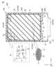
図1は、本実施形態の表示装置DSPの一構成例を示す平面図である。一例では、第1方向X、第2方向Y、および、第3方向Zは、互いに直交しているが、90度以外の角度で交差していてもよい。第1方向Xおよび第2方向Yは、表示装置DSPを構成する基板の主面と平行な方向に相当し、第3方向Zは、表示装置DSPの厚さ方向に相当する。本明細書において、第1基板SUB1から第2基板SUB2に向かう方向を「上側」(あるいは、単に上)と称し、第2基板SUB2から第1基板SUB1に向かう方向を「下側」(あるいは、単に下)と称する。「第1部材の上の第2部材」および「第1部材の下の第2部材」とした場合、第2部材は、第1部材に接していてもよいし、第1部材から離間していてもよい。また、第3方向Zを示す矢印の先端側に表示装置DSPを観察する観察位置があるものとし、この観察位置から、第1方向Xおよび第2方向Yで規定されるX-Y平面に向かって見ることを平面視と言う。 First Embodiment
FIG. 1 is a plan view showing a configuration example of the display device DSP of this embodiment. In one example, the first direction X, the second direction Y, and the third direction Z are orthogonal to each other, but may intersect at an angle other than 90 degrees. The first direction X and the second direction Y correspond to a direction parallel to the main surface of the substrate constituting the display device DSP, and the third direction Z corresponds to the thickness direction of the display device DSP. In this specification, the direction from the first substrate SUB1 to the second substrate SUB2 is referred to as the "upper side" (or simply "upper"), and the direction from the second substrate SUB2 to the first substrate SUB1 is referred to as the "lower side" (or simply "lower"). When the "second member above the first member" and the "second member below the first member" are used, the second member may be in contact with the first member or may be spaced apart from the first member. In addition, the observation position for observing the display device DSP is located at the tip of the arrow indicating the third direction Z, and looking from this observation position toward the XY plane defined by the first direction X and the second direction Y is called planar view.
本実施形態においては、表示装置DSPの一例として、高分子分散型液晶を適用した液晶表示装置(透明ディスプレイ)について説明する。図1に示すように、表示装置DSPは、表示パネルPNLと、第1配線基板LED FPCとを備えている。In this embodiment, a liquid crystal display device (transparent display) that uses polymer-dispersed liquid crystal will be described as an example of the display device DSP. As shown in FIG. 1, the display device DSP includes a display panel PNL and a first wiring board LED FPC.
表示パネルPNLは、第1基板SUB1と、第2基板SUB2と、液晶層LCと、シールSEと、を備えている。第1基板SUB1および第2基板SUB2は、X-Y平面と平行な平板状に形成されている。第1基板SUB1および第2基板SUB2は、平面視において重畳している。第1基板SUB1および第2基板SUB2は、シールSEによって接着されている。液晶層LCは、第1基板SUB1と第2基板SUB2との間に保持され、シールSEによって封止されている。図1において、液晶層LCおよびシールSEは、異なる斜線で示している。The display panel PNL comprises a first substrate SUB1, a second substrate SUB2, a liquid crystal layer LC, and a seal SE. The first substrate SUB1 and the second substrate SUB2 are formed in the shape of flat plates parallel to the XY plane. The first substrate SUB1 and the second substrate SUB2 overlap in a planar view. The first substrate SUB1 and the second substrate SUB2 are bonded together by the seal SE. The liquid crystal layer LC is held between the first substrate SUB1 and the second substrate SUB2, and is sealed by the seal SE. In FIG. 1, the liquid crystal layer LC and the seal SE are indicated by different diagonal lines.
図1において拡大して模式的に示すように、液晶層LCは、ポリマー31と、液晶分子32とを含む高分子分散型液晶を備えている。一例では、ポリマー31は、液晶性ポリマーである。ポリマー31は、筋状に延出している。ポリマー31の延出方向D1は、第1方向Xと平行である。液晶分子32は、ポリマー31の隙間に分散され、その長軸が第1方向Xに沿うように配向される。ポリマー31および液晶分子32の各々は、光学異方性あるいは屈折率異方性を有している。ポリマー31の電界に対する応答性は、液晶分子32の電界に対する応答性より低い。As shown enlarged and schematic in FIG. 1, the liquid crystal layer LC comprises a polymer-dispersed liquid crystal including a
一例では、ポリマー31の配向方向は、電界の有無にかかわらずほとんど変化しない。一方で、液晶分子32の配向方向は、液晶層LCにしきい値以上の高い電圧が印加された状態では、電界に応じて変化する。液晶層LCに電圧が印加されていない状態では、ポリマー31および液晶分子32のそれぞれの光軸は互いに平行であり、液晶層LCに入射した光は、液晶層LC内でほとんど散乱されることなく透過する(透明状態)。液晶層LCに電圧が印加された状態では、ポリマー31および液晶分子32のそれぞれの光軸は互いに交差し、液晶層LCに入射した光は、液晶層LC内で散乱される(散乱状態)。In one example, the orientation direction of the
表示パネルPNLは、画像を表示する表示部DAと、表示部DAを囲む額縁状の非表示部NDAとを備えている。シールSEは、非表示部NDAに位置している。表示部DAは、第1方向Xおよび第2方向Yにマトリクス状に配列された画素PXを備えている。The display panel PNL has a display section DA that displays an image and a frame-shaped non-display section NDA that surrounds the display section DA. The seal SE is located in the non-display section NDA. The display section DA has pixels PX arranged in a matrix in the first direction X and the second direction Y.
図1において拡大して示すように、各画素PXは、スイッチング素子SW、画素電極PE、共通電極CE、液晶層LC、などを備えている。スイッチング素子SWは、例えば薄膜トランジスタ(TFT)によって構成され、走査線Gおよび信号線Sと電気的に接続されている。走査線Gは、第1方向Xに並んだ画素PXの各々におけるスイッチング素子SWと電気的に接続されている。信号線Sは、第2方向Yに並んだ画素PXの各々におけるスイッチング素子SWと電気的に接続されている。画素電極PEは、スイッチング素子SWと電気的に接続されている。画素電極PEの各々は、共通電極CEと対向し、画素電極PEと共通電極CEとの間に生じる液晶層LC(特に、液晶分子32)を駆動している。容量CSは、例えば、共通電極CEと同電位の電極と、画素電極PEと同電位の電極との間に形成される。As shown enlarged in FIG. 1, each pixel PX includes a switching element SW, a pixel electrode PE, a common electrode CE, a liquid crystal layer LC, and the like. The switching element SW is, for example, a thin film transistor (TFT) and is electrically connected to a scanning line G and a signal line S. The scanning line G is electrically connected to the switching element SW in each of the pixels PX aligned in the first direction X. The signal line S is electrically connected to the switching element SW in each of the pixels PX aligned in the second direction Y. The pixel electrode PE is electrically connected to the switching element SW. Each pixel electrode PE faces the common electrode CE and drives the liquid crystal layer LC (particularly, liquid crystal molecules 32) generated between the pixel electrode PE and the common electrode CE. The capacitance CS is formed, for example, between an electrode having the same potential as the common electrode CE and an electrode having the same potential as the pixel electrode PE.
第1基板SUB1は、第1方向Xに沿って延出した端部E11およびE12と、第2方向Yに沿って延出した端部E13およびE14とを有している。端部E11は第1端部と称されてもよい。The first substrate SUB1 has ends E11 and E12 extending along the first direction X, and ends E13 and E14 extending along the second direction Y. End E11 may be referred to as the first end.
第2基板SUB2は、少なくとも一部が第1方向Xに沿って延出した端部E21と、第1方向Xに沿って延出した端部E22と、第2方向Yに沿って延出した端部E23およびE24とを有している。端部E21は第2端部と称されてもよい。端部E21は凹部を有している。より詳しくは、端部E21は、第1方向Xに沿って延出した第1辺s1、第2辺s2および第3辺s3と、第1辺s1および第2辺s2を繋ぐ第1斜辺s4と、第2辺s2および第3辺s3を繋ぐ第2斜辺s5と、を有しており、第2辺s2と第1斜辺s4と第2斜辺s5とによりテーパ状の凹部を形成している。The second substrate SUB2 has an end E21 at least a part of which extends along the first direction X, an end E22 which extends along the first direction X, and ends E23 and E24 which extend along the second direction Y. End E21 may be referred to as a second end. End E21 has a recess. More specifically, end E21 has a first side s1, a second side s2, and a third side s3 which extend along the first direction X, a first oblique side s4 which connects the first side s1 and the second side s2, and a second oblique side s5 which connects the second side s2 and the third side s3, and the second side s2, the first oblique side s4, and the second oblique side s5 form a tapered recess.
図示した例では、端部E12およびE22と、端部E13およびE23と、端部E14およびE24とは、平面視においてそれぞれ重畳している。端部E21は、平面視において、端部E11と表示部DA(液晶層LC)との間に位置している。第1基板SUB1は、端部E11と端部E21との間に延出部Exを有している。延出部Exは第1領域と称されてもよい。In the illustrated example, ends E12 and E22, ends E13 and E23, and ends E14 and E24 overlap each other in a planar view. End E21 is located between end E11 and the display unit DA (liquid crystal layer LC) in a planar view. The first substrate SUB1 has an extension portion Ex between end E11 and end E21. The extension portion Ex may be referred to as the first region.
第1配線基板LED FPCは、後述する発光素子LEDと電気的に接続されている。第1配線基板LED FPCは、折り曲げ可能なフレキシブルプリント回路基板である。第1配線基板LED FPCは、第2基板SUB2の端部E21に沿った形状を有している。つまり、第1配線基板LED FPCは、第2基板SUB2の端部E21の凹部と平面視において重畳する凸部を有している。The first wiring board LED FPC is electrically connected to the light-emitting element LED, which will be described later. The first wiring board LED FPC is a bendable flexible printed circuit board. The first wiring board LED FPC has a shape that conforms to the end E21 of the second board SUB2. In other words, the first wiring board LED FPC has a convex portion that overlaps in a plan view with the concave portion of the end E21 of the second board SUB2.
図2は、図1に示した表示パネルPNLの一構成例を示す断面図である。図2では、表示部DAの断面を示している。
第1基板SUB1は、透明基板10と、絶縁膜11および12と、容量電極13と、スイッチング素子SWと、画素電極PEと、配向膜AL1と、を備えている。透明基板10は第1透明基板と称されてもよい。なお、図2では図示を省略しているが、第1基板SUB1は、図1に示した走査線Gおよび信号線Sをさらに備えている。透明基板10は、主面(下面)10Aと、主面10Aの反対側の主面(上面)10Bとを備えている。スイッチング素子SWは、主面10Bに配置されている。絶縁膜11は、スイッチング素子SWを覆っている。容量電極13は、絶縁膜11および12の間に位置している。画素電極PEは、絶縁膜12の上において、画素PX毎に配置されている。画素電極PEは、容量電極13の開口部OPを介してスイッチング素子SWと電気的に接続されている。画素電極PEは、絶縁膜12を挟んで、容量電極13と重畳し、画素PXの容量CSを形成している。配向膜AL1は、画素電極PEを覆っている。 Fig. 2 is a cross-sectional view showing an example of the configuration of the display panel PNL shown in Fig. 1. Fig. 2 shows a cross section of the display area DA.
The first substrate SUB1 includes a
第2基板SUB2は、透明基板20と、遮光層BMと、共通電極CEと、配向膜AL2と、を備えている。透明基板20は第2透明基板と称されてもよい。透明基板20は、主面(下面)20Aと、主面20Aの反対側の主面(上面)20Bとを備えている。透明基板20の主面20Aは、透明基板10の主面10Bと向かい合っている。遮光層BMおよび共通電極CEは、主面20Aに配置されている。遮光層BMは、例えば、スイッチング素子SWの真上、および、図示しない走査線Gおよび信号線Sの真上にそれぞれ位置している。共通電極CEは、複数の画素PXに亘って配置され、遮光層BMを直接覆っている。共通電極CEは、容量電極13と電気的に接続されており、容量電極13とは同電位である。配向膜AL2は、共通電極CEを覆っている。液晶層LCは、主面10Bと主面20Aとの間に位置し、配向膜AL1およびAL2に接している。第1基板SUB1において、絶縁膜11および12、容量電極13、スイッチング素子SW、画素電極PE、および、配向膜AL1は、主面10Bと液晶層LCとの間に位置している。第2基板SUB2において、遮光層BM、共通電極CEおよび配向膜AL2は、主面20Aと液晶層LCとの間に位置している。The second substrate SUB2 includes a
透明基板10および20は、ガラス基板やプラスチック基板などの絶縁基板である。主面10Aおよび10B、主面20Aおよび20Bは、X-Y平面と略平行な面である。絶縁膜11はシリコン酸化物、シリコン窒化物、シリコン酸窒化物、アクリル樹脂などの透明な絶縁材料によって形成されている。一例では、絶縁膜11は、無機絶縁膜および有機絶縁膜を含んでいる。絶縁膜12は、シリコン窒化物などの無機絶縁膜である。容量電極13、画素電極PEおよび共通電極CEは、インジウム錫酸化物(ITO)やインジウム亜鉛酸化物(IZO)などの透明導電材料によって形成された透明電極である。遮光層BMは、例えば、共通電極CEよりも低抵抗な導電層である。一例では、遮光層BMは、モリブデン、アルミニウム、タングステン、チタン、銀などの不透明な金属材料によって形成されている。配向膜AL1およびAL2は、X-Y平面に略平行な配向規制力を有する水平配向膜である。一例では、配向膜AL1およびAL2は、第1方向Xに沿って配向処理されている。なお、配向処理とは、ラビング処理であってもよいし、光配向処理であってもよい。The
図3は、本実施形態の表示装置DSPの一構成例を示す別の平面図である。図3では、図1に示した第1配線基板LED FPCの図示を省略し、第1配線基板LED FPCの下方に位置する各種構成と、第2基板SUB2の上方に位置するカバー部材CMとを図示している。Figure 3 is another plan view showing an example of the configuration of the display device DSP of this embodiment. In Figure 3, the first wiring board LED FPC shown in Figure 1 is omitted, and various components located below the first wiring board LED FPC and a cover member CM located above the second substrate SUB2 are shown.
図3に示すように、表示装置DSPは、第1ドライバ1、第2ドライバ2、異方性導電膜ACF1、第2配線基板FPC、異方性導電膜ACF2、カバー部材CM、導光板LGおよび複数の発光素子LEDをさらに備えている。カバー部材CMは第3透明基板と称されてもよい。As shown in FIG. 3, the display device DSP further includes a
第1ドライバ1および第2ドライバ2は、異方性導電膜ACF1を介して第1基板SUB1の延出部Exの上に実装されている。第1ドライバ1は、例えば、信号線Sを駆動し、画素PXに映像信号を出力するように構成される信号線駆動回路として機能する。第2ドライバ2は、例えば、走査線Gを駆動するように構成される走査線駆動回路として機能する。第2配線基板FPCは、異方性導電膜ACF2を介して第1基板SUB1の延出部Exの上に実装されている。第2配線基板FPCは、折り曲げ可能なフレキシブルプリント回路基板である。第2配線基板FPCは、図示しない回路基板と電気的に接続されている。第1ドライバ1および第2ドライバ2は、第2配線基板FPCを介して図示しない回路基板と電気的に接続されている。なお、第1ドライバ1および第2ドライバ2は、第2配線基板FPC上に実装されてもよい。The
カバー部材CMは、第2基板SUB2の透明基板20の主面20Bの上に配置されている。カバー部材CMは、平面視において第2基板SUB2(透明基板20)と重畳している。カバー部材CMは、例えば、透明ガラスやポリメタクリル酸メチル(PMMA)、ポリカーボネイト(PC)などの透明樹脂によって形成されている。カバー部材CMは、少なくとも一部が第1方向Xに沿って延出した端部ECM1と、第1方向Xに沿って延出した端部ECM2と、第2方向Yに沿って延出した端部ECM3およびECM4とを有している。端部ECM1は第3端部と称されてもよい。図示した例では、端部E21およびECM1と、端部E22およびECM2と、端部E23およびECM3と、端部E24およびECM4とは、平面視においてそれぞれ重畳している。つまり、端部ECM1は、端部E21同様、テーパ状に形成された凹部を有している。The cover member CM is disposed on the
導光板LGは、カバー部材CMの端部ECM1に沿って延出した多面体状に形成されている。導光板LGは、端部E21およびECM1の凹部と平面視において重畳する凸部と、当該凸部に対向する凹部とを有した多面体状に形成されている。導光板LGは、カバー部材CMおよび第2基板SUB2(透明基板20)と、複数の発光素子LEDとの間に位置している。The light guide plate LG is formed in a polyhedral shape extending along the end ECM1 of the cover member CM. The light guide plate LG is formed in a polyhedral shape having a convex portion that overlaps the concave portion of the end E21 and ECM1 in a plan view, and a concave portion facing the convex portion. The light guide plate LG is located between the cover member CM and the second substrate SUB2 (transparent substrate 20) and the multiple light emitting elements LED.
複数の発光素子LEDは、導光板LGを形成する多数の面のうち、端部ECM1に沿って延出した複数の面とそれぞれ対向する複数の面に沿って間隔をおいて並んでいる。複数の発光素子LEDは、第1基板SUB1の延出部Exの上方に配置され、図1に示した第1配線基板LED FPCと電気的に接続されている。複数の発光素子LEDは、例えば、発光ダイオードである。複数の発光素子LEDから照射される光は、導光板LGを通って、カバー部材CMの端部ECM1および第2基板SUB2の端部E21より表示パネルPNLに入射される。The multiple light-emitting elements LED are arranged at intervals along multiple surfaces that face the multiple surfaces extending along the end ECM1, among the many surfaces that form the light guide plate LG. The multiple light-emitting elements LED are arranged above the extension portion Ex of the first substrate SUB1 and are electrically connected to the first wiring substrate LED FPC shown in FIG. 1. The multiple light-emitting elements LED are, for example, light-emitting diodes. Light emitted from the multiple light-emitting elements LED passes through the light guide plate LG and is incident on the display panel PNL from the end ECM1 of the cover member CM and the end E21 of the second substrate SUB2.
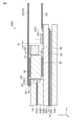
図4は、図1および図3に示した表示装置DSPの延出部Ex周辺を拡大した断面図であり、図3に示すA-B線に沿って表示装置DSPを切断した場合の断面図である。
図4に示すように、表示装置DSPは、透明接着層OCA1、タッチパネルフィルムTF、タッチパネルカバー部材TCM、透明接着層OCA2、接着層AD1、接着層AD2、接着層AD3および接続層LAをさらに備えている。 FIG. 4 is an enlarged cross-sectional view of the periphery of the extension portion Ex of the display device DSP shown in FIGS. 1 and 3, and is a cross-sectional view of the display device DSP cut along the line AB shown in FIG.
As shown in FIG. 4, the display device DSP further includes a transparent adhesive layer OCA1, a touch panel film TF, a touch panel cover member TCM, a transparent adhesive layer OCA2, an adhesive layer AD1, an adhesive layer AD2, an adhesive layer AD3, and a connection layer LA.
第1基板SUB1の下方には、透明接着層OCA1、タッチパネルフィルムTF、タッチパネルカバー部材TCMが順に積層されている。タッチパネルフィルムTFは、透明接着層OCA1を介して第1基板SUB1の主面10Aに接着されている。タッチパネルフィルムTFは、例えば二層積層構造を有し、タッチパネルTPおよび接着層AD4を有している。タッチパネルカバー部材TCMは、タッチパネルフィルムTFの接着層AD4によりタッチパネルフィルムTFに接着されている。Below the first substrate SUB1, a transparent adhesive layer OCA1, a touch panel film TF, and a touch panel cover member TCM are laminated in this order. The touch panel film TF is adhered to the
透明接着層OCA2は、第2基板SUB2とカバー部材CMとの間に位置し、第2基板SUB2とカバー部材CMとを接着している。透明接着層OCA2は、第2基板SUB2の主面20Bの略全面に亘って設けられている。The transparent adhesive layer OCA2 is located between the second substrate SUB2 and the cover member CM, and bonds the second substrate SUB2 to the cover member CM. The transparent adhesive layer OCA2 is provided over substantially the entire
接着層AD1は、カバー部材CMと第1配線基板LED FPCとを接着している。接着層AD2は、導光板LGと第1基板SUB1とを接着している。接着層AD3は、導光板LGと第1配線基板LED FPCとを接着している。接着層AD1は反射部材M1を備え、接着層AD2は反射部材M2を備え、接着層AD3は反射部材M3を備えている。接着層AD1,AD2,AD3は、例えば、接着剤、反射部材、接着剤の順に積層された積層体である。接着層AD1,AD2,AD3は、例えば、両面テープで形成されている。反射部材M1,M2,M3は、例えば、アルミニウム、モリブデン、チタン、銀などの高反射率の金属材料によって形成されている。
接続層LAは、第1配線基板LED FPCと発光素子LEDとを電気的に接続している。接続層LAは半田によって形成されている。 The adhesive layer AD1 bonds the cover member CM and the first wiring board LED FPC. The adhesive layer AD2 bonds the light guide plate LG and the first substrate SUB1. The adhesive layer AD3 bonds the light guide plate LG and the first wiring board LED FPC. The adhesive layer AD1 includes a reflective member M1, the adhesive layer AD2 includes a reflective member M2, and the adhesive layer AD3 includes a reflective member M3. The adhesive layers AD1, AD2, and AD3 are, for example, a laminate in which an adhesive, a reflective member, and an adhesive are laminated in this order. The adhesive layers AD1, AD2, and AD3 are, for example, formed of a double-sided tape. The reflective members M1, M2, and M3 are, for example, formed of a metal material with high reflectivity, such as aluminum, molybdenum, titanium, or silver.
The connection layer LA electrically connects the first wiring board LED FPC and the light emitting element LED. The connection layer LA is made of solder.
図4に示すように、発光素子LEDは、接続層LAを介して第1配線基板LED FPCに実装されている。発光素子LEDは、導光板LGを挟んで、カバー部材CMの端部ECM1および第2基板SUB2の端部E21と対向している。発光素子LEDから照射される光は、導光板LGの一方の面から入射すると、導光板LGの上面および下面で反射されながら導光板LG内を進行していく。導光板LG内を進行してきた光は、導光板LGの他方の面から出射され、カバー部材CMの端部ECM1および第2基板SUB2の端部E21からカバー部材CMおよび第2基板SUB2に入射される。As shown in FIG. 4, the light-emitting element LED is mounted on the first wiring board LED FPC via the connection layer LA. The light-emitting element LED faces the end ECM1 of the cover member CM and the end E21 of the second substrate SUB2 across the light guide plate LG. When the light emitted from the light-emitting element LED enters one side of the light guide plate LG, it travels through the light guide plate LG while being reflected by the upper and lower surfaces of the light guide plate LG. The light that has traveled through the light guide plate LG is emitted from the other side of the light guide plate LG and is incident on the cover member CM and the second substrate SUB2 from the end ECM1 of the cover member CM and the end E21 of the second substrate SUB2.
なお、導光板LG内を進行していく光のうち、導光板LGの下面を透過した光は、接着層AD2の反射部材M2によって反射され、再度導光板LG内に戻り、導光板LG内を進行していく。このため、導光板LG内を進行していく光は、第1基板SUB1に設けられる金属配線には届かない。これによれば、導光板LG内を進行していく光が、第1基板SUB1に設けられる金属配線により散乱してしまうことを抑制することができ、表示品位の低下を抑制することができる。Of the light traveling through the light guide plate LG, light that passes through the lower surface of the light guide plate LG is reflected by the reflecting member M2 of the adhesive layer AD2, returns to the light guide plate LG, and travels through the light guide plate LG. For this reason, the light traveling through the light guide plate LG does not reach the metal wiring provided on the first substrate SUB1. This makes it possible to prevent the light traveling through the light guide plate LG from being scattered by the metal wiring provided on the first substrate SUB1, and thus to prevent a decrease in display quality.
また、導光板LG内を進行していく光のうち、導光板LGの上面を透過した光は、接着層AD3の反射部材M3によって反射され、再度導光板LG内に戻り、導光板LG内を進行していく。このため、導光板LG内を進行していく光は、第1配線基板LED FPCには届かない。これによれば、導光板LG内を進行していく光が、第1配線基板LED FPCにより散乱してしまうことを抑制することができ、表示品位の低下を抑制することができる。In addition, of the light traveling through the light guide plate LG, the light that passes through the upper surface of the light guide plate LG is reflected by the reflecting member M3 of the adhesive layer AD3, returns to the light guide plate LG, and travels through the light guide plate LG. Therefore, the light traveling through the light guide plate LG does not reach the first wiring board LED FPC. This makes it possible to prevent the light traveling through the light guide plate LG from being scattered by the first wiring board LED FPC, and thus to prevent a decrease in display quality.
なお、上記した接着層AD1の反射部材M1にはグレー印刷が施されていることが望ましい。これによれば、カバー部材CMおよび第2基板SUB2に入射される光の明度を調整することが可能である。具体的には、カバー部材CMおよび第2基板SUB2に入射される光のうち、接着層AD1の反射部材M1において反射される光の明度を抑制することが可能である。It is preferable that the reflective member M1 of the adhesive layer AD1 described above is printed in gray. This makes it possible to adjust the brightness of the light incident on the cover member CM and the second substrate SUB2. Specifically, it is possible to suppress the brightness of the light reflected by the reflective member M1 of the adhesive layer AD1 out of the light incident on the cover member CM and the second substrate SUB2.
図4に示すように、本実施形態に係る表示装置DSPは、発光素子LEDと第1ドライバ1との間に距離d1の間隔(スペース)を有している。距離d1は、カバー部材CMの端部ECM1と、第2基板SUB2の端部E21とが有する凹部の深さ(第2方向Yの長さ)に近似する。つまり、本実施形態に係る表示装置DSPは、カバー部材CMの端部ECM1と、第2基板SUB2の端部E21とに形成された凹部の深さ分だけ、発光素子LEDと第1ドライバ1とを離して配置することができる。これによれば、発光素子LEDが点灯することにより生じる熱や、第1ドライバ1が駆動することにより生じる熱を、上記したスペースにおいて十分に放熱することができ、例えば、第1ドライバ1の温度が耐熱温度を超え、壊れてしまうなどの不具合を抑制することができる。As shown in FIG. 4, the display device DSP according to this embodiment has a distance (space) of d1 between the light-emitting element LED and the
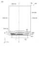
ここで、比較例を用いて、本実施形態に係る表示装置DSPの効果について説明する。なお、比較例は、本実施形態に係る表示装置DSPが奏し得る効果の一部を説明するためのものであって、比較例と本実施形態とで共通する効果を本願発明の範囲から除外するものではない。Here, the effects of the display device DSP according to this embodiment will be explained using a comparative example. Note that the comparative example is intended to explain some of the effects that can be achieved by the display device DSP according to this embodiment, and does not exclude effects common to the comparative example and this embodiment from the scope of the present invention.
図5は比較例に係る表示装置DSPaの平面図であり、図6は比較例に係る表示装置DSPaの断面図である。比較例に係る表示装置DSPaは、図5および図6に示すように、カバー部材CMおよび第2基板SUB2が矩形である点で、本実施形態と相違している。また、カバー部材CMおよび第2基板SUB2が矩形であることから、導光板LGは直方体状であり、複数の発光素子LEDが直方体状の導光板LGに沿って、換言すると、第1方向Xに沿って、間隔をおいて並んでいる点でも、本実施形態と相違している。Figure 5 is a plan view of a display device DSPa according to a comparative example, and Figure 6 is a cross-sectional view of the display device DSPa according to the comparative example. As shown in Figures 5 and 6, the display device DSPa according to the comparative example differs from this embodiment in that the cover member CM and the second substrate SUB2 are rectangular. In addition, since the cover member CM and the second substrate SUB2 are rectangular, the light guide plate LG is rectangular, and the multiple light-emitting elements LED are arranged at intervals along the rectangular light guide plate LG, in other words, along the first direction X, which also differs from this embodiment.
比較例に係る表示装置DSPaは、カバー部材CMおよび第2基板SUB2が矩形であり、導光板LGが直方体状であることから、図5および図6に示すように、発光素子LEDと第1ドライバ1との間には、距離da(<d1)の間隔しか設けられていない。これによれば、発光素子LEDが点灯することにより生じる熱や、第1ドライバ1が駆動することにより生じる熱を、十分に放熱することができず、第1ドライバ1の温度が耐熱温度を超え、壊れてしまうなどの不具合が発生する恐れがある。In the display device DSPa of the comparative example, the cover member CM and the second substrate SUB2 are rectangular, and the light guide plate LG is rectangular, so that there is only a distance da (<d1) between the light-emitting element LED and the
これに対し、本実施形態に係る表示装置DSPにおいては、カバー部材CMの端部ECM1と、第2基板SUB2の端部E21とのうちの第1ドライバ1と対向する部分に、テーパ状の凹部が形成されている。このテーパ状の凹部は、およそ距離d1(>da)の深さを有している。また、本実施形態に係る表示装置DSPにおいては、導光板LGはカバー部材CMの端部ECM1および第2基板SUB2の端部E21に形成されたテーパ状の凹部に対応した形状を有している。このため、カバー部材CMの端部ECM1と、第2基板SUB2の端部E21とに形成された凹部の深さに近似した距離だけ、発光素子LEDと第1ドライバ1とを離して配置することができる。これによれば、発光素子LEDが点灯することにより生じる熱や、第1ドライバ1が駆動することにより生じる熱を、上記したスペースにおいて十分に放熱することができ、上記した不具合の発生を抑制することが可能である。In contrast, in the display device DSP according to this embodiment, a tapered recess is formed in the end ECM1 of the cover member CM and the end E21 of the second substrate SUB2, which are opposed to the
なお、本実施形態においては、表示装置DSPは、カバー部材CMの端部ECM1と、第2基板SUB2の端部E21とのうちの第1ドライバ1と対向する部分に、テーパ状の凹部を有しているとしたが、カバー部材CMの端部ECM1と第2基板SUB2の端部E21とに形成される凹部の形状は、発光素子LEDと第1ドライバ1とを離して配置することが可能な形状であればテーパ状でなくてもよく、例えば半球状凹型など、任意の形状であって構わない。In this embodiment, the display device DSP has tapered recesses in the end ECM1 of the cover member CM and the end E21 of the second substrate SUB2, which face the
<第2の実施形態>
次に、第2の実施形態について説明する。第2の実施形態に係る表示装置DSP1は、カバー部材CMおよび第2基板SUBと発光素子LEDとの間に、導光板LGが設けられていない点で、上記した第1の実施形態の表示装置DSPと相違している。以下では、基本的に、上記した第1の実施形態と相違している点について説明する。 Second Embodiment
Next, a second embodiment will be described. The display device DSP1 according to the second embodiment differs from the display device DSP of the first embodiment described above in that the light guide plate LG is not provided between the cover member CM and the second substrate SUB and the light emitting element LED. Below, the differences from the first embodiment described above will basically be described.
図7は、本実施形態の表示装置DSP1の一構成例を示す平面図である。図7に示すように、表示装置DSP1においては、上記した第1の実施形態と同様に、カバー部材CMの端部ECM1と第2基板SUB2の端部E21とのうちの第1ドライバ1と対向する部分に、テーパ状の凹部が形成されている。一方で、図7に示すように、本実施形態に係る表示装置DSP1は導光板LGを備えていないため、本実施形態に係る表示装置DSP1においては、複数の発光素子LEDは、カバー部材CMの端部ECM1と第2基板SUB2の端部E21とに沿って間隔をおいて並んでいる。Figure 7 is a plan view showing one configuration example of the display device DSP1 of this embodiment. As shown in Figure 7, in the display device DSP1, similar to the first embodiment described above, a tapered recess is formed in the portion of the end ECM1 of the cover member CM and the end E21 of the second substrate SUB2 that faces the
図8は、図7に示すE-F線に沿って表示装置DSP1を切断した場合の断面図である。図8に示すように、発光素子LEDは、カバー部材CMの端部ECM1および第2基板SUB2の端部E21と対向している。図示した例では、発光素子LEDと、カバー部材CMの端部ECM1および第2基板SUB2の端部E21との間には、例えば、0.2mm以下の距離を有した間隔が設けられている。なお、発光素子LEDと、カバー部材CMの端部ECM1および第2基板SUB2の端部E21との間の距離はゼロであっても構わない。つまり、発光素子LEDと、カバー部材CMの端部ECM1および第2基板SUB2の端部E21とは接していても構わない。Figure 8 is a cross-sectional view of the display device DSP1 cut along line E-F shown in Figure 7. As shown in Figure 8, the light-emitting element LED faces the end ECM1 of the cover member CM and the end E21 of the second substrate SUB2. In the illustrated example, a gap of, for example, 0.2 mm or less is provided between the light-emitting element LED and the end ECM1 of the cover member CM and the end E21 of the second substrate SUB2. Note that the distance between the light-emitting element LED and the end ECM1 of the cover member CM and the end E21 of the second substrate SUB2 may be zero. In other words, the light-emitting element LED may be in contact with the end ECM1 of the cover member CM and the end E21 of the second substrate SUB2.
図8に示すように、本実施形態に係る表示装置DSP1は、発光素子LEDと第1ドライバ1との間に距離d2(>d1)の間隔(スペース)を有している。距離d2は、カバー部材CMの端部ECM1と、第2基板SUB2の端部E21とに形成された凹部の深さと、上記した第1の実施形態に示す導光板LGの幅(第2方向Yの長さ)との和に近似する。As shown in FIG. 8, the display device DSP1 according to this embodiment has a distance (space) of d2 (>d1) between the light-emitting element LED and the
以上説明した第2の実施形態によれば、表示装置DSP1は、カバー部材CMの端部ECM1と、第2基板SUB2の端部E21とに形成された凹部の深さと、上記した第1の実施形態に示す導光板LGの幅との和に近似する距離だけ、発光素子LEDと第1ドライバ1とを離して配置することができる。これによれば、発光素子LEDが点灯することにより生じる熱や、第1ドライバ1が駆動することにより生じる熱を、上記したスペースにおいて十分に放熱することができ、上記した不具合の発生を抑制することが可能である。According to the second embodiment described above, the display device DSP1 can arrange the light-emitting element LED and the
また、第2の実施形態によれば、発光素子LEDから照射される光は、カバー部材CMの端部ECM1および第2基板SUB2の端部E21からカバー部材CMおよび第2基板SUB2に直接入射される。これによれば、カバー部材CMおよび第2基板SUB2に対して、減衰していない光を入射させることができ、導光板LGを介してカバー部材CMおよび第2基板SUB2に光を入射させる場合に比べて、輝度向上を図ることが可能である。つまり、表示装置DSP1の表示品位を向上させることが可能である。Furthermore, according to the second embodiment, the light emitted from the light-emitting element LED is directly incident on the cover member CM and the second substrate SUB2 from the end ECM1 of the cover member CM and the end E21 of the second substrate SUB2. This allows unattenuated light to be incident on the cover member CM and the second substrate SUB2, and it is possible to improve the brightness compared to the case where light is incident on the cover member CM and the second substrate SUB2 via the light guide plate LG. In other words, it is possible to improve the display quality of the display device DSP1.
<第3の実施形態>
次に、第3の実施形態について説明する。第3の実施形態に係る表示装置DSP2は、発光素子LEDと第1ドライバ1との間に、放熱部材TIMが設けられている点で、上記した第2の実施形態の表示装置DSP1と相違している。以下では、基本的に、上記した第2の実施形態と相違している点について説明する。 Third Embodiment
Next, a third embodiment will be described. The display device DSP2 according to the third embodiment differs from the display device DSP1 according to the second embodiment in that a heat dissipation member TIM is provided between the light emitting element LED and the
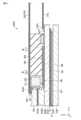
図9は、本実施形態の表示装置DSP2の一構成例を示す平面図である。図9に示すように、表示装置DSP2においては、上記した第2の実施形態と同様に、カバー部材CMの端部ECM1と第2基板SUB2の端部E21とのうちの第1ドライバ1と対向する部分に、テーパ状の凹部が形成されている。また、表示装置DSP2においては、上記した第2の実施形態と同様に、複数の発光素子LEDは、カバー部材CMの端部ECM1と第2基板SUB2の端部E21とに沿って間隔をおいて並んでいる。一方で、図9に示すように、本実施形態に係る表示装置DSP2においては、発光素子LEDと第1ドライバ1との間に、放熱部材TIMが設けられている。9 is a plan view showing an example of the configuration of the display device DSP2 of this embodiment. As shown in FIG. 9, in the display device DSP2, similar to the second embodiment described above, a tapered recess is formed in the portion of the end ECM1 of the cover member CM and the end E21 of the second substrate SUB2 that faces the
図10は、図9に示すG-H線に沿って表示装置DSP2を切断した場合の断面図である。図10に示すように、本実施形態に係る表示装置DSP2は、発光素子LEDと第1ドライバ1との間に放熱部材TIMを備えている。放熱効率の観点から、放熱部材TIMの上面は、第1配線基板LED FPCと当接している方が望ましい。放熱部材TIMは、第1配線基板LED FPCを介して外部に熱を放熱可能な材料で形成されていればよく、例えば樹脂材料や金属材料によって形成されている。Figure 10 is a cross-sectional view of the display device DSP2 cut along line G-H shown in Figure 9. As shown in Figure 10, the display device DSP2 according to this embodiment includes a heat dissipation member TIM between the light-emitting element LED and the
放熱部材TIMは、接着層AD5を介して第1基板SUB1の延出部Exに接着されている。接着層AD5は、第2基板SUB2の端部E21と、第1ドライバ1との間に設けられている。接着層AD5は、反射部材M5を備えており、例えば、接着剤、反射部材、接着剤の順に積層された積層体である。反射部材M5は、例えば、アルミニウム、モリブデン、チタン、銀などの高反射率の金属材料によって形成されている。The heat dissipation member TIM is adhered to the extension portion Ex of the first substrate SUB1 via an adhesive layer AD5. The adhesive layer AD5 is provided between the end portion E21 of the second substrate SUB2 and the
以上説明した第3の実施形態によれば、表示装置DSP2は、カバー部材CMの端部ECM1と、第2基板SUB2の端部E21とにテーパ状の凹部を形成し、かつ、導光板LGを設けないことにより空いたスペースに配置された放熱部材TIMを備えている。これによれば、図10の矢印に示すように、発光素子LEDが点灯することにより生じる熱や、第1ドライバ1が駆動することにより生じる熱を、第1配線基板LED FPCを介して外部に放熱することができ、上記した不具合の発生を抑制することが可能である。According to the third embodiment described above, the display device DSP2 has tapered recesses formed in the end ECM1 of the cover member CM and the end E21 of the second substrate SUB2, and is equipped with a heat dissipation member TIM arranged in the space created by not providing a light guide plate LG. As a result, as shown by the arrows in Figure 10, heat generated by the light-emitting element LED being turned on and heat generated by the
また、第3の実施形態によれば、表示装置DSP2は、発光素子LEDの下方にまで延在し、かつ、反射部材M5を有する接着層AD5を備えている。反射部材M5は、発光素子LEDの下方に照射される光を反射し、主に第2基板SUB2の端部E21から第2基板SUB2に入射させる。これによれば、反射部材M5を有する接着層AD5が発光素子LEDの下方に設けられていない場合に比べて、カバー部材CMおよび第2基板SUB2に光を入射させることができ、輝度向上を図ることが可能である。つまり、表示装置DSP2の表示品位を向上させることが可能である。Furthermore, according to the third embodiment, the display device DSP2 includes an adhesive layer AD5 that extends below the light-emitting element LED and has a reflective member M5. The reflective member M5 reflects light that is irradiated below the light-emitting element LED, and causes the light to enter the second substrate SUB2 mainly from the end E21 of the second substrate SUB2. As a result, compared to a case in which the adhesive layer AD5 having the reflective member M5 is not provided below the light-emitting element LED, light can be made to enter the cover member CM and the second substrate SUB2, and brightness can be improved. In other words, the display quality of the display device DSP2 can be improved.
なお、発光素子LEDと第1ドライバ1との間に設けられる放熱部材TIMは、例えば図11に示すように、第1ドライバ1を覆うように設けられてもよい。このように第1ドライバ1を放熱部材TIMにより覆ってしまうことにより、外部から水分が侵入し、第1ドライバ1を腐食させてしまうような不具合の発生を抑制することが可能である。The heat dissipation member TIM provided between the light-emitting element LED and the
以上説明した少なくとも一つの実施形態によれば、光源が点灯することにより生じる熱や、各種ドライバが駆動することにより生じる熱を放熱可能な透明ディスプレイ(表示装置)を提供することが可能である。According to at least one of the embodiments described above, it is possible to provide a transparent display (display device) that can dissipate heat generated when a light source is turned on and when various drivers are operated.
本発明のいくつかの実施形態を説明したが、これらの実施形態は、例として提示したものであり、発明の範囲を限定することは意図していない。これら新規な実施形態は、その他の様々な形態で実施されることが可能であり、発明の要旨を逸脱しない範囲で、種々の省略、置き換え、変更を行うことができる。これら実施形態やその変形は、発明の範囲や要旨に含まれるとともに、特許請求の範囲に記載された発明とその均等の範囲に含まれる。Although several embodiments of the present invention have been described, these embodiments are presented as examples and are not intended to limit the scope of the invention. These novel embodiments can be implemented in various other forms, and various omissions, substitutions, and modifications can be made without departing from the gist of the invention. These embodiments and their modifications are included in the scope and gist of the invention, and are included in the scope of the invention and its equivalents described in the claims.
DSP1…表示装置、PNL…表示パネル、1…第1ドライバ、SUB1…第1基板、SUB2…第2基板、CM…カバー部材、Ex…延出部、LED…発光素子、E21,ECM1…端部。DSP1...display device, PNL...display panel, 1...first driver, SUB1...first board, SUB2...second board, CM...cover member, Ex...extension, LED...light-emitting element, E21, ECM1...end portion.
Claims (14)
Translated fromJapanese第2端部を有し、かつ、前記第1透明基板に対向する第2透明基板と、
前記第2端部に沿って設けられる複数の発光素子と、
前記第2端部と前記複数の発光素子との間に設けられる導光板と、
を具備し、
前記第1透明基板は、
前記第1端部と、前記第2端部との間の領域であって、前記第2透明基板と平面視で重畳しない第1領域に設けられる第1ドライバを備え、
前記第2端部は、第1凹部を有し、
前記導光板は、前記第1凹部と平面視で重畳する凸部と、前記凸部に対向する第2凹部とを有し、
前記複数の発光素子のうち、前記第2凹部に沿って設けられる少なくとも一つ以上の第1発光素子は、前記第1ドライバとの間に所定の間隔を有して対向している、
表示装置。 a first transparent substrate having a first edge;
a second transparent substrate having a second end portion and facing the first transparent substrate;
a plurality of light emitting elements disposed along the second end;
a light guide plate provided between the second end and the plurality of light emitting elements;
Equipped with
The first transparent substrate is
a first driver provided in a first region between the first end and the second end, the first region not overlapping with the second transparent substrate in a plan view;
the second end has afirst recess;
the light guide plate has a convex portion overlapping the first concave portion in a plan view and a second concave portion facing the convex portion,
Among the plurality of light-emitting elements, at least one first light-emitting element provided along thesecond recess faces the first driver with a predetermined interval therebetween.
Display device.
前記第3端部は、前記第1凹部に沿う形状を有し、
前記第1凹部は、前記第2端部および前記第3端部に形成されている、
請求項1に記載の表示装置。 a third transparent substrate having a third end portion and facing the second transparent substrate;
The third end portion has a shape that fits alongthe first recess portion,
Thefirst recess is formed in the second end and the third end.
The display device according to claim 1 .
前記第1端部と、前記第2端部および前記第3端部とは平面視で重畳しない、
請求項2に記載の表示装置。 the second end and the third end overlap each other in a plan view,
The first end portion does not overlap with the second end portion and the third end portion in a plan view.
The display device according to claim 2 .
請求項2に記載の表示装置。 The light emitting device further includes a heat dissipation member provided between the first light emitting element and the first driver.
The display device according to claim 2 .
請求項4に記載の表示装置。 The heat dissipation member covers the first driver.
The display device according to claim 4.
請求項4または請求項5に記載の表示装置。 a reflecting member provided between the second end and the first driver and extending below the plurality of light-emitting elements and the heat dissipation member;
The display device according to claim 4 or 5.
請求項6に記載の表示装置。 The reflective member overlaps with the plurality of light-emitting elements in a plan view.
The display device according to claim 6.
請求項2に記載の表示装置。 The plurality of light emitting elements face the second end and the third end.
The display device according to claim 2 .
請求項8に記載の表示装置。 A distance between the plurality of light-emitting elements and the second end and between the plurality of light-emitting elements and the third end is 0.2 mm or less.
The display device according to claim 8.
請求項9に記載の表示装置。 The plurality of light-emitting elements are in contact with the second end and the third end.
The display device according to claim 9.
請求項2~請求項10のいずれか1項に記載の表示装置。 The plurality of light-emitting elements are electrically connected to a first wiring substrate provided on the third transparent substrate.
The display device according to any one of claims 2 to 10.
第2端部を有し、かつ、前記第1透明基板に対向する第2透明基板と、
前記第2端部に沿って設けられる複数の発光素子と、
第3端部を有し、かつ、前記第2透明基板に対向する第3透明基板と、
を具備し、
前記第1透明基板は、
前記第1端部と、前記第2端部との間の領域であって、前記第2透明基板と平面視で重畳しない第1領域に設けられる第1ドライバを備え、
前記第2端部は、凹部を有し、
前記複数の発光素子のうち、前記凹部に沿って設けられる少なくとも一つ以上の第1発光素子は、前記第1ドライバとの間に所定の間隔を有して対向し、
前記第3端部は、前記凹部に沿う形状を有し、
前記凹部は、前記第2端部および前記第3端部に形成され、
前記複数の発光素子は、前記第3透明基板の上に設けられる第1配線基板と電気的に接続され、
前記第3透明基板と前記第1配線基板とは、前記第3透明基板上に設けられた接着層を介して接着される、
表示装置。a first transparent substrate having a first edge;
a second transparent substrate having a second end portion and facing the first transparent substrate;
a plurality of light emitting elements disposed along the second end;
a third transparent substrate having a third end portion and facing the second transparent substrate;
Equipped with
The first transparent substrate is
a first driver provided in a first region between the first end and the second end, the first region not overlapping with the second transparent substrate in a plan view;
The second end has a recess.
Among the plurality of light-emitting elements, at least one first light-emitting element provided along the recess faces the first driver with a predetermined interval therebetween;
The third end portion has a shape that fits along the recessed portion,
the recess is formed in the second end and the third end,
the plurality of light-emitting elements are electrically connected to a first wiring substrate provided on the third transparent substrate;
The third transparent substrate and the first wiring substrate are bonded to each other via an adhesive layer provided on the third transparent substrate.
Display device.
請求項12に記載の表示装置。 the first wiring substrate has a protrusion that overlaps the recess in a plan view;
The display device according to claim 12.
請求項2~請求項13のいずれか1項に記載の表示装置。 The first driver outputs a video signal to a plurality of pixels arranged in a matrix.
The display device according to any one of claims 2 to 13.
Priority Applications (2)
| Application Number | Priority Date | Filing Date | Title |
|---|---|---|---|
| JP2020089672AJP7467231B2 (en) | 2020-05-22 | 2020-05-22 | Display device |
| US17/326,420US11556027B2 (en) | 2020-05-22 | 2021-05-21 | Display device |
Applications Claiming Priority (1)
| Application Number | Priority Date | Filing Date | Title |
|---|---|---|---|
| JP2020089672AJP7467231B2 (en) | 2020-05-22 | 2020-05-22 | Display device |
Publications (2)
| Publication Number | Publication Date |
|---|---|
| JP2021184052A JP2021184052A (en) | 2021-12-02 |
| JP7467231B2true JP7467231B2 (en) | 2024-04-15 |
Family
ID=78608874
Family Applications (1)
| Application Number | Title | Priority Date | Filing Date |
|---|---|---|---|
| JP2020089672AActiveJP7467231B2 (en) | 2020-05-22 | 2020-05-22 | Display device |
Country Status (2)
| Country | Link |
|---|---|
| US (1) | US11556027B2 (en) |
| JP (1) | JP7467231B2 (en) |
Families Citing this family (3)
| Publication number | Priority date | Publication date | Assignee | Title |
|---|---|---|---|---|
| JP2023167048A (en) | 2022-05-11 | 2023-11-24 | 株式会社ジャパンディスプレイ | Liquid crystal display device and display device |
| JP2023167047A (en) | 2022-05-11 | 2023-11-24 | 株式会社ジャパンディスプレイ | liquid crystal display device |
| JP2024047598A (en) | 2022-09-27 | 2024-04-08 | 株式会社ジャパンディスプレイ | Mounting structure of transparent liquid crystal display device |
Citations (12)
| Publication number | Priority date | Publication date | Assignee | Title |
|---|---|---|---|---|
| JP2000180851A (en) | 1998-12-11 | 2000-06-30 | Rohm Co Ltd | Construction of backlight liquid crystal display device |
| JP2002156919A (en) | 2000-11-22 | 2002-05-31 | Matsushita Electric Ind Co Ltd | Film liquid crystal module |
| JP2004309774A (en) | 2003-04-07 | 2004-11-04 | Citizen Watch Co Ltd | Liquid crystal device |
| JP2007129067A (en) | 2005-11-04 | 2007-05-24 | Epson Imaging Devices Corp | Board, electrooptical device, electronic apparatus, and method of manufacturing electrooptical device |
| JP2009037179A (en) | 2007-08-02 | 2009-02-19 | Samsung Sdi Co Ltd | Plasma display device |
| US20120057367A1 (en) | 2010-09-02 | 2012-03-08 | Jun Seok Park | Backlight unit |
| JP2012113919A (en) | 2010-11-24 | 2012-06-14 | Toshiba Corp | Lighting device |
| CN204790052U (en) | 2015-06-23 | 2015-11-18 | 深圳Tcl新技术有限公司 | Poor light module and liquid crystal display device |
| JP2016139094A (en) | 2015-01-29 | 2016-08-04 | セイコーエプソン株式会社 | Display device and electronic apparatus |
| US20180092207A1 (en) | 2016-09-27 | 2018-03-29 | Samsung Display Co., Ltd. | Backlight unit including curved light source unit and display apparatus having the same |
| WO2019136952A1 (en) | 2018-01-10 | 2019-07-18 | 北京小米移动软件有限公司 | Lcd display module and mobile terminal |
| JP2019219440A (en) | 2018-06-15 | 2019-12-26 | 株式会社ジャパンディスプレイ | Display device |
Family Cites Families (6)
| Publication number | Priority date | Publication date | Assignee | Title |
|---|---|---|---|---|
| JPH11125816A (en)* | 1997-10-21 | 1999-05-11 | Rohm Co Ltd | Structure for backlight liquid crystal display device |
| TWI266120B (en)* | 2003-07-18 | 2006-11-11 | Hon Hai Prec Ind Co Ltd | Back light module and liquid crystal display using the same |
| BRPI1008027A2 (en)* | 2009-02-10 | 2016-03-15 | Sharp Kk | liquid crystal display device |
| JP7043204B2 (en)* | 2017-09-12 | 2022-03-29 | 株式会社ジャパンディスプレイ | Display device |
| JP2019191230A (en) | 2018-04-19 | 2019-10-31 | 株式会社ジャパンディスプレイ | Display device |
| JP2020160322A (en)* | 2019-03-27 | 2020-10-01 | 株式会社ジャパンディスプレイ | Display |
- 2020
- 2020-05-22JPJP2020089672Apatent/JP7467231B2/enactiveActive
- 2021
- 2021-05-21USUS17/326,420patent/US11556027B2/enactiveActive
Patent Citations (12)
| Publication number | Priority date | Publication date | Assignee | Title |
|---|---|---|---|---|
| JP2000180851A (en) | 1998-12-11 | 2000-06-30 | Rohm Co Ltd | Construction of backlight liquid crystal display device |
| JP2002156919A (en) | 2000-11-22 | 2002-05-31 | Matsushita Electric Ind Co Ltd | Film liquid crystal module |
| JP2004309774A (en) | 2003-04-07 | 2004-11-04 | Citizen Watch Co Ltd | Liquid crystal device |
| JP2007129067A (en) | 2005-11-04 | 2007-05-24 | Epson Imaging Devices Corp | Board, electrooptical device, electronic apparatus, and method of manufacturing electrooptical device |
| JP2009037179A (en) | 2007-08-02 | 2009-02-19 | Samsung Sdi Co Ltd | Plasma display device |
| US20120057367A1 (en) | 2010-09-02 | 2012-03-08 | Jun Seok Park | Backlight unit |
| JP2012113919A (en) | 2010-11-24 | 2012-06-14 | Toshiba Corp | Lighting device |
| JP2016139094A (en) | 2015-01-29 | 2016-08-04 | セイコーエプソン株式会社 | Display device and electronic apparatus |
| CN204790052U (en) | 2015-06-23 | 2015-11-18 | 深圳Tcl新技术有限公司 | Poor light module and liquid crystal display device |
| US20180092207A1 (en) | 2016-09-27 | 2018-03-29 | Samsung Display Co., Ltd. | Backlight unit including curved light source unit and display apparatus having the same |
| WO2019136952A1 (en) | 2018-01-10 | 2019-07-18 | 北京小米移动软件有限公司 | Lcd display module and mobile terminal |
| JP2019219440A (en) | 2018-06-15 | 2019-12-26 | 株式会社ジャパンディスプレイ | Display device |
Also Published As
| Publication number | Publication date |
|---|---|
| JP2021184052A (en) | 2021-12-02 |
| US20210364849A1 (en) | 2021-11-25 |
| US11556027B2 (en) | 2023-01-17 |
Similar Documents
| Publication | Publication Date | Title |
|---|---|---|
| US12392955B2 (en) | Display device | |
| JP7467231B2 (en) | Display device | |
| US11181784B2 (en) | Display device | |
| US12386229B2 (en) | Display device | |
| JP2020177731A (en) | Cover glass and display device | |
| WO2020246066A1 (en) | Display device | |
| JP7638794B2 (en) | Display device | |
| JP7505044B2 (en) | Display device | |
| JP7246888B2 (en) | Display device and lighting device | |
| US11609463B2 (en) | Display device | |
| US12306491B2 (en) | Display device | |
| JP7326558B2 (en) | Display device | |
| US20250284155A1 (en) | Liquid crystal display device | |
| JP7159101B2 (en) | Display device | |
| CN111679519B (en) | display device | |
| JP7242340B2 (en) | Display device | |
| JP2025008896A (en) | Display device | |
| JP2023180535A (en) | Display device, light guide plate, and display device manufacturing method | |
| JP2024141827A (en) | Illumination and display devices | |
| JP2024078136A (en) | Display device and cover glass |
Legal Events
| Date | Code | Title | Description |
|---|---|---|---|
| A621 | Written request for application examination | Free format text:JAPANESE INTERMEDIATE CODE: A621 Effective date:20230419 | |
| A977 | Report on retrieval | Free format text:JAPANESE INTERMEDIATE CODE: A971007 Effective date:20231227 | |
| A131 | Notification of reasons for refusal | Free format text:JAPANESE INTERMEDIATE CODE: A131 Effective date:20240116 | |
| A521 | Request for written amendment filed | Free format text:JAPANESE INTERMEDIATE CODE: A523 Effective date:20240313 | |
| TRDD | Decision of grant or rejection written | ||
| A01 | Written decision to grant a patent or to grant a registration (utility model) | Free format text:JAPANESE INTERMEDIATE CODE: A01 Effective date:20240319 | |
| A61 | First payment of annual fees (during grant procedure) | Free format text:JAPANESE INTERMEDIATE CODE: A61 Effective date:20240403 | |
| R150 | Certificate of patent or registration of utility model | Ref document number:7467231 Country of ref document:JP Free format text:JAPANESE INTERMEDIATE CODE: R150 | |
| S111 | Request for change of ownership or part of ownership | Free format text:JAPANESE INTERMEDIATE CODE: R313113 | |
| R350 | Written notification of registration of transfer | Free format text:JAPANESE INTERMEDIATE CODE: R350 |