JP7466386B2 - Optical transmission module and electronic control device - Google Patents
Optical transmission module and electronic control deviceDownload PDFInfo
- Publication number
- JP7466386B2 JP7466386B2JP2020102498AJP2020102498AJP7466386B2JP 7466386 B2JP7466386 B2JP 7466386B2JP 2020102498 AJP2020102498 AJP 2020102498AJP 2020102498 AJP2020102498 AJP 2020102498AJP 7466386 B2JP7466386 B2JP 7466386B2
- Authority
- JP
- Japan
- Prior art keywords
- transmission module
- optical transmission
- photoelectric conversion
- external
- island
- Prior art date
- Legal status (The legal status is an assumption and is not a legal conclusion. Google has not performed a legal analysis and makes no representation as to the accuracy of the status listed.)
- Active
Links
Images


Classifications
- G—PHYSICS
- G02—OPTICS
- G02B—OPTICAL ELEMENTS, SYSTEMS OR APPARATUS
- G02B6/00—Light guides; Structural details of arrangements comprising light guides and other optical elements, e.g. couplings
- G02B6/24—Coupling light guides
- G02B6/42—Coupling light guides with opto-electronic elements
- G02B6/4201—Packages, e.g. shape, construction, internal or external details
- G02B6/4274—Electrical aspects
- G02B6/4277—Protection against electromagnetic interference [EMI], e.g. shielding means
- G—PHYSICS
- G02—OPTICS
- G02B—OPTICAL ELEMENTS, SYSTEMS OR APPARATUS
- G02B6/00—Light guides; Structural details of arrangements comprising light guides and other optical elements, e.g. couplings
- G02B6/24—Coupling light guides
- G02B6/42—Coupling light guides with opto-electronic elements
- G02B6/4201—Packages, e.g. shape, construction, internal or external details
- G02B6/4246—Bidirectionally operating package structures
- G—PHYSICS
- G02—OPTICS
- G02B—OPTICAL ELEMENTS, SYSTEMS OR APPARATUS
- G02B6/00—Light guides; Structural details of arrangements comprising light guides and other optical elements, e.g. couplings
- G02B6/24—Coupling light guides
- G02B6/42—Coupling light guides with opto-electronic elements
- G02B6/4292—Coupling light guides with opto-electronic elements the light guide being disconnectable from the opto-electronic element, e.g. mutually self aligning arrangements
- H—ELECTRICITY
- H01—ELECTRIC ELEMENTS
- H01L—SEMICONDUCTOR DEVICES NOT COVERED BY CLASS H10
- H01L2224/00—Indexing scheme for arrangements for connecting or disconnecting semiconductor or solid-state bodies and methods related thereto as covered by H01L24/00
- H01L2224/01—Means for bonding being attached to, or being formed on, the surface to be connected, e.g. chip-to-package, die-attach, "first-level" interconnects; Manufacturing methods related thereto
- H01L2224/42—Wire connectors; Manufacturing methods related thereto
- H01L2224/47—Structure, shape, material or disposition of the wire connectors after the connecting process
- H01L2224/48—Structure, shape, material or disposition of the wire connectors after the connecting process of an individual wire connector
- H01L2224/4805—Shape
- H01L2224/4809—Loop shape
- H01L2224/48091—Arched
- H—ELECTRICITY
- H01—ELECTRIC ELEMENTS
- H01L—SEMICONDUCTOR DEVICES NOT COVERED BY CLASS H10
- H01L2924/00—Indexing scheme for arrangements or methods for connecting or disconnecting semiconductor or solid-state bodies as covered by H01L24/00
- H01L2924/30—Technical effects
- H01L2924/301—Electrical effects
- H01L2924/3025—Electromagnetic shielding
Landscapes
- Physics & Mathematics (AREA)
- General Physics & Mathematics (AREA)
- Optics & Photonics (AREA)
- Electromagnetism (AREA)
- Semiconductor Lasers (AREA)
- Light Receiving Elements (AREA)
- Shielding Devices Or Components To Electric Or Magnetic Fields (AREA)
- Optical Couplings Of Light Guides (AREA)
Description
Translated fromJapaneseこの明細書における開示は、光伝送モジュールおよび電子制御装置に関する。The disclosure in this specification relates to an optical transmission module and an electronic control device.
特許文献1は、光伝送モジュールを開示している。先行技術文献の記載内容は、この明細書における技術的要素の説明として、参照により援用される。
特許文献1では、多層基板のグランド層が、金属ケースに電気的に接続されている。このため、電磁波ノイズにより、多層基板に実装された駆動回路部品、ひいては光部品が誤動作する虞がある。上述の観点において、または言及されていない他の観点において、光伝送モジュールにはさらなる改良が求められている。In
開示されるひとつの目的は、電磁波ノイズによる誤動作を抑制できる光伝送モジュールを提供することにある。One disclosed objective is to provide an optical transmission module that can suppress malfunctions caused by electromagnetic noise.
開示される他のひとつの目的は、光伝送モジュールを備えた電子制御装置において、電磁波ノイズによる誤動作を抑制することにある。Another disclosed objective is to suppress malfunctions caused by electromagnetic noise in electronic control devices equipped with optical transmission modules.
ここに開示された光伝送モジュールは、
グランドパターン(220)を含む導体パターン(22)を備えたプリント基板(20)と、
プリント基板に実装されており、開口(310a)を通じて外部コネクタ(17)が嵌合する嵌合部(312)を備えたハウジング(31)と、ハウジングに収容されており、外部コネクタが光学的に結合する端子部(32)と、を有する光コネクタ(30)と、
端子部に光学的に結合された光電変換素子(42)と、光電変換素子およびグランドパターンのそれぞれに電気的に接続された回路部(41、43)を有し、開口に対して端子部よりも奥側でハウジングに収容された光電変換部(40)と、
電磁遮蔽性を有し、端子部および光電変換部を取り囲むように配置されたシールド部材(50)と、
を備え、
シールド部材は、グランドパターンとは電気的に分離されており、
プリント基板は、導体パターンとして、プリント基板の板厚方向からの平面視において嵌合部と重なる位置に、グランドパターンとは電気的に分離されたアイランド(223)を有している。 The optical transmission module disclosed herein comprises:
A printed circuit board (20) having a conductor pattern (22) including a ground pattern (220);
An optical connector (30) having a housing (31) mounted on a printed circuit board and having a fitting portion (312) into which an external connector (17) fits through an opening (310a), and a terminal portion (32) accommodated in the housing and optically coupled to the external connector;
a photoelectric conversion unit (40) having a photoelectric conversion element (42) optically coupled to the terminal portion and a circuit portion (41, 43) electrically connected to the photoelectric conversion element and the ground pattern, respectively, and accommodated in the housing on the inner side of the opening relative to the terminal portion;
a shielding member (50) having electromagnetic shielding properties and arranged to surround the terminal portion and the photoelectric conversion portion;
Equipped with
The shielding material is electrically isolated from the ground pattern.
The printed circuit board has, as a conductor pattern, an island (223) electrically isolated from the ground pattern at a position overlapping the fitting portion in a plan view from the thickness direction of the printed circuit board.
開示の光伝送モジュールによると、シールド部材を、プリント基板のグランドパターンに対して電気的に分離している。これにより、電磁波ノイズが、シールド部材から、光電変換部に伝搬するのを抑制することができる。また、ハウジングの嵌合部と重なる位置に設けたアイランドを、グランドパターンに対して電気的に分離している。これにより、電磁波ノイズの伝搬を抑制する効果を高めることができる。この結果、電磁波ノイズによる誤動作を抑制できる光伝送モジュールを提供することができる。According to the disclosed optical transmission module, the shielding member is electrically isolated from the ground pattern of the printed circuit board. This makes it possible to suppress the propagation of electromagnetic noise from the shielding member to the photoelectric conversion section. In addition, the island provided at a position overlapping with the fitting section of the housing is electrically isolated from the ground pattern. This makes it possible to enhance the effect of suppressing the propagation of electromagnetic noise. As a result, it is possible to provide an optical transmission module that can suppress malfunctions caused by electromagnetic noise.
ここに開示された電子制御装置は、
請求項1~7いずれか1項に記載の光伝送モジュール(12)と、
光伝送モジュールを介して外部機器(6)と光通信可能に接続される制御回路(14)と、
を備える。 The electronic control device disclosed herein comprises:
An optical transmission module (12) according to any one of
A control circuit (14) that is optically communicably connected to an external device (6) via an optical transmission module;
Equipped with.
開示の電子制御装置は、上記した光伝送モジュールを備えている。よって、光伝送モジュールを備えた電子制御装置において、電磁波ノイズによる誤動作を抑制することができる。The disclosed electronic control device includes the optical transmission module described above. Therefore, in an electronic control device that includes an optical transmission module, malfunctions caused by electromagnetic noise can be suppressed.
この明細書における開示された複数の態様は、それぞれの目的を達成するために、互いに異なる技術的手段を採用する。請求の範囲およびこの項に記載した括弧内の符号は、後述する実施形態の部分との対応関係を例示的に示すものであって、技術的範囲を限定することを意図するものではない。この明細書に開示される目的、特徴、および効果は、後続の詳細な説明、および添付の図面を参照することによってより明確になる。The various aspects disclosed in this specification employ different technical means to achieve their respective objectives. The claims and the reference characters in parentheses in this section are illustrative of the corresponding relationships with the embodiments described below, and are not intended to limit the technical scope. The objectives, features, and advantages disclosed in this specification will become clearer with reference to the detailed description that follows and the accompanying drawings.
以下、図面に基づいて複数の実施形態を説明する。なお、各実施形態において対応する構成要素には同一の符号を付すことにより、重複する説明を省略する場合がある。各実施形態において構成の一部分のみを説明している場合、当該構成の他の部分については、先行して説明した他の実施形態の構成を適用することができる。また、各実施形態の説明において明示している構成の組み合わせばかりではなく、特に組み合わせに支障が生じなければ、明示していなくても複数の実施形態の構成同士を部分的に組み合せることができる。Below, several embodiments will be described with reference to the drawings. Note that in each embodiment, corresponding components are given the same reference numerals, and duplicated descriptions may be omitted. When only a portion of the configuration is described in each embodiment, the configuration of the other embodiment described above can be applied to the other portions of the configuration. In addition to the combinations of configurations explicitly stated in the description of each embodiment, configurations of several embodiments can be partially combined together even if not explicitly stated, as long as there is no particular problem with the combination.
(第1実施形態)
本実施形態に係る光伝送モジュールおよび電子制御装置は、たとえば移動体に適用可能である。移動体は、車両、ドローンなどの飛行体、船舶、建設機械、農業機械である。以下では、車両に適用される例について説明する。なお、光伝送モジュールおよび電子制御装置を、移動体以外の用途に適用してもよい。 First Embodiment
The optical transmission module and electronic control device according to the present embodiment can be applied to, for example, a moving body. The moving body is a vehicle, an aircraft such as a drone, a ship, a construction machine, or an agricultural machine. An example of application to a vehicle will be described below. Note that the optical transmission module and electronic control device may be applied to applications other than the moving body.
<電子制御装置>
先ず、図1に基づき、電子制御装置10の概略構成について説明する。図1では、便宜上、電源回路13からの電源供給ラインの図示を省略している。図1に示すように、電子制御装置10は、コネクタ11と、光伝送モジュール12と、電源回路13と、制御回路14と、通信回路15、16を備えている。 <Electronic control device>
First, a schematic configuration of an
電子制御装置10(ECU)は、コネクタ11および光伝送モジュール12を介して、車両に搭載された他の機器と接続される。ECUは、electronic control unitの略称である。コネクタ11(CN)は、電子制御装置10において他の機器との電気的な接続を提供する。コネクタ11には、ワイヤハーネス1を介して、バッテリ2(BAT)が接続される。バッテリ2は、車両に搭載された直流電圧源である。電子制御装置10は、コネクタ11およびワイヤハーネス1を介して、バッテリ2からの電力供給が可能に構成されている。電力は、コネクタ11を介して、電源回路13に供給される。The electronic control unit 10 (ECU) is connected to other devices mounted on the vehicle via a connector 11 and an
電源回路13(PWR)は、バッテリ2の直流電圧を異なる値の直流電圧に変換する。電源回路13は、バッテリ2の直流電圧から、電子制御装置10において必要とされる所定の電圧を生成し、光伝送モジュール12、制御回路14、通信回路15、16などへ供給する。The power supply circuit 13 (PWR) converts the DC voltage of the
コネクタ11には、ワイヤハーネス3を介して、バッテリ2とは別の機器である外部機器4(EX1)が接続される。コネクタ11には、少なくともひとつの外部機器4が接続される。コネクタ11には、複数の外部機器4が接続されてもよい。電子制御装置10は、外部機器4と通信可能に接続される。外部機器4は、たとえば、アクチュエータなどの制御対象機器、センサ、および他の電子制御装置の少なくともひとつを含む。An external device 4 (EX1), which is a device separate from the
光伝送モジュール12(OTM)は、電子制御装置10において他の機器との光学的な接続を提供する。光伝送モジュール12には、光ファイバケーブル5を介して、外部機器6(EX2)が接続される。光伝送モジュール12には、少なくともひとつの外部機器6が接続される。光伝送モジュール12には、複数の外部機器6が接続されてもよい。電子制御装置10は、外部機器6と光通信可能に接続される。制御回路14は、光伝送モジュール12を介して外部機器6と光通信可能に接続される。電子制御装置10と外部機器6との通信のほうが、電子制御装置10と外部機器4との通信よりも高速である。The optical transmission module 12 (OTM) provides the
外部機器6は、たとえば、自車両の周辺を監視する周辺監視センサである。外部機器6は、周辺監視センサとして、自車両周辺の所定範囲を撮像する周辺監視カメラ、ミリ波レーダ、ソナー、および道路形状および構造物の特徴点の点群を検出するLiDARの少なくともひとつを含む。LiDARは、Light Detection and Ranging/Laser Imaging Detection and Rangingの略称である。The
制御回路14(CTR)は、プロセッサ、メモリ、入出力インターフェース、およびこれらを接続するバスを備えるマイクロコンピュータを主体として構成されている。プロセッサが、メモリに格納された制御プログラムを実行することで各種の処理を実行する。制御回路14は、対応する通信回路15、16を介して、外部機器4、6の少なくともひとつからデータを取得し、取得したデータを用いて処理を実行する。そして、処理結果を、対応する通信回路15、16を介して、外部機器4、6の少なくともひとつに送信する。The control circuit 14 (CTR) is mainly composed of a microcomputer equipped with a processor, memory, an input/output interface, and a bus connecting these. The processor executes various processes by running control programs stored in the memory. The
通信回路15(COM1)および通信回路16(COM2)のひとつは、少なくとも送信機能を有し、他のひとつは少なくとも受信機能を有する。通信回路15、16のそれぞれが、送信機能および受信機能を有してもよい。通信回路15、16は、送信機能のみを有する場合に送信回路、受信機能のみ有する場合に受信回路、送受信機能を有する場合に送受信回路(トランシーバ)と称されることがある。One of communication circuits 15 (COM1) and 16 (COM2) has at least a transmitting function, and the other has at least a receiving function. Each of
電子制御装置10は、たとえば周辺監視ECUである。外部機器4は、走行支援ECUなどの他の電子制御装置を含む。外部機器6は、周辺監視カメラなどの周辺監視センサを含む。制御回路14は、光伝送モジュール12および通信回路16を介して、周辺監視センサの検出信号(たとえば画像データ)を取得する。制御回路14は、取得した画像データを解析処理することで、自車両の進行経路上の障害物や、自車両の周辺に存在する移動体の有無およびその位置、進行方向等を認識する。自車両の周辺に存在する移動体は、自動車および軽車両等の他車両や、歩行者等を含む。周辺監視ECUは、障害物に関する情報や移動体に関する情報などを、通信回路15およびコネクタ11を介して、外部機器4(他の電子制御装置)へと逐次提供する。The
電子制御装置10は、たとえば走行制御ECUである。外部機器4は、アクチュエータとして、EPSモータ、電子スロットルモータ、ブレーキアクチュエータなどを含む。EPSは、Electric Power Steeringの略称である。外部機器4は、センサとして、車速センサ、舵角センサなどを含む。外部機器6は、周辺監視カメラなどの周辺監視センサを含む。制御回路14は、コネクタ11および通信回路15を介して、舵角センサ、車速センサなどの検出信号を取得する。制御回路14は、光伝送モジュール12および通信回路16を介して、周辺監視センサの検出信号を取得する。制御回路14は、取得した検出信号を用いて処理を実行し、通信回路15およびコネクタ11を介して、各アクチュエータに制御信号を出力する。制御回路14は、たとえば自車両の進行経路上に障害物を認識した場合、障害物との衝突を回避するようにアクチュエータを制御する。The
<光伝送モジュール>
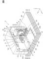
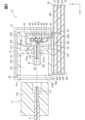
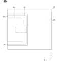
次に、図2~図9に基づき、光伝送モジュール12について説明する。図2は、光伝送モジュールの概略構成を示す斜視図である。図2では、内部構造を示すため、一部の要素を部分的に断面で示している。図3は、図2のIII-III線に沿う断面図である。図3では、光コネクタに嵌合する外部コネクタについても、簡素化しつつ図示している。図4は、光コネクタの嵌合部および端子部と、プリント基板のアイランドとの位置関係を示す図である。図4では、Z方向から平面視したときの嵌合部の位置を破線で示している。同様に、端子部の位置を一点鎖線で示している。図4では、便宜上、グランドパターンとアイランド以外の導体パターンを省略している。 <Optical transmission module>
Next, the
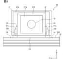
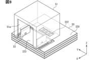
図5は、図2をX1方向から見た構造の一例を示す平面図である。図5では、便宜上、光コネクタの端子部を簡素化している。また、外部シールド内の構造を示すために、外部シールドを簡素化して図示している。図6は、プリント基板に実装されたペグを示す斜視図である。図6では、ペグの構造を示すために、光コネクタの他の要素を省略して図示している。図7は、図5とは別例を示す図である。図7では、光電変換部の構造を示すために、光コネクタの端子部およびハウジングの隔壁、内部シールドのリッドを省略して図示している。図8は、外部シールドを示す斜視図である。図9は、外部シールドの固定構造を示す斜視図である。便宜上、プリント基板上に配置される要素として、ペグと外部シールドのみを示している。Figure 5 is a plan view showing an example of the structure of Figure 2 as seen from the X1 direction. In Figure 5, the terminal portion of the optical connector is simplified for convenience. Also, the external shield is simplified to show the structure inside the external shield. Figure 6 is a perspective view showing a peg mounted on a printed circuit board. In Figure 6, other elements of the optical connector are omitted to show the structure of the peg. Figure 7 is a view showing another example from Figure 5. In Figure 7, the terminal portion of the optical connector, the bulkhead of the housing, and the lid of the internal shield are omitted to show the structure of the photoelectric conversion unit. Figure 8 is a perspective view showing the external shield. Figure 9 is a perspective view showing the fixing structure of the external shield. For convenience, only the peg and the external shield are shown as elements arranged on the printed circuit board.
図2および図3に示すように、光伝送モジュール12は、プリント基板20と、光コネクタ30と、光電変換部40と、シールド部材50を備えている。以下において、プリント基板20の板厚方向をZ方向と示す。Z方向に直交する一方向をX方向と示す。Z方向およびX方向の両方向に直交する方向をY方向と示す。特に断りのない限り、Z方向から平面視した形状、換言すればX方向およびY方向により規定されるXY平面に沿う形状、を平面形状と示す。また、Z方向からの平面視を、単に平面視と示すことがある。As shown in Figures 2 and 3, the
プリント基板20は、樹脂などを材料とする絶縁基材21と、絶縁基材21に配置された導体パターン22を有している。導体パターン22は、たとえば金属箔をパターニングすることで形成されている。Z方向においてプリント基板20の一面側に、光伝送モジュール12を構成する他の要素、すなわち、光コネクタ30、光電変換部40、およびシールド部材50が配置されている。The printed
導体パターン22は、Z方向においてプリント基板20の一面に配置されている。導体パターン22は、絶縁基材21に対して多層に配置されてもよい。たとえば、プリント基板20の両面に配置されてもよいし、内層パターンを含んでもよい。本実施形態の導体パターン22は、絶縁基材21に対して4層配置である。プリント基板20の表面に配置される導体パターン22のうち、接続箇所以外の部分は、ソルダレジスト等によって覆われてもよい。本実施形態では、便宜上、ソルダレジストを省略して図示している。The
導体パターン22は、配線機能を提供する。導体パターン22は、外部機器6と通信回路16とを電気的に接続するための配線を含む。プリント基板20には、上記したコネクタ11、電源回路13、制御回路14、通信回路15、および通信回路16の少なくともひとつが実装されてもよい。この場合、導体パターン22は、実装された要素と他の要素とを電気的に接続するための配線を含む。The
導体パターン22は、グランド(GND)パターン220と、図示しない電源パターンと、シグナルパターン221と、複数のパッド222を有している。グランドパターン220は、光伝送モジュール12において基準電位を提供する導体パターンである。グランドパターン220は、比較的面積の大きい所謂ベタパターンを含む。本実施形態のグランドパターン220は、各層に設けられている。グランドパターン220は、グランドライン、グランドプレーンと称されることがある。The
シグナルパターン221は、信号を伝送するための導体パターンである。シグナルパターン221は、伝送ライン、シグナルライン、信号配線と称されることがある。パッド222は、光電変換部40のリード端子44が接続される端子部である。パッド222は、ランドと称されることがある。パッド222は、プリント基板20の一面に設けられている。パッド222は、図示しない電源パッドと、グランドパッド222aと、シグナルパッド222bを含む。本実施形態において、複数のパッド222は、所定ピッチを有してY方向に一列に配置されている。The
プリント基板20の一面において、パッド222の周囲にはグランドパターン220が配置されている。導体パターン22においてパッド222の周囲に溝が形成されることで、パッド222とグランドパターン220とが電気的に分離されている。パッド222は、たとえば、接続ビア23を介して、内層の対応する導体パターン22に接続されている。図3に示すように、たとえばシグナルパッド222bは、接続ビア23を介して内層のシグナルパターン221に電気的に接続されている。On one side of the printed
導体パターン22は、さらにアイランド223を有している。アイランド223は、他の導体パターン22とは電気的に分離されている。アイランド223は、プリント基板20の一面に配置されている。導体パターン22においてアイランド223の周囲に溝24が形成されることで、アイランド223とグランドパターン220とが電気的に分離されている。溝24は、たとえばエッチングにより導体パターン22が除去された領域である。The
図2および図4に示すように、本実施形態のアイランド223は、X方向を短手方向、Y方向を長手方向とする平面略長方形をなしている。アイランド223の長辺のひとつが、平面略矩形状をなすプリント基板20の辺のひとつ、すなわち一端20aに接している。アイランド223の残りの3辺とグランドパターン220との間に、溝24が設けられている。溝24は、平面略コの字(U字状)をなしている。2 and 4, the
アイランド223は、Z方向からの平面視において、嵌合部312の少なくとも一部と重なるように配置されている。本実施形態では、図4に示すように、アイランド223が、後述する嵌合部312のほぼ全域と重なるように配置されている。アイランド223は、平面視において端子部32の主たる部分と重なるように配置されている。アイランド223は、平面視において嵌合部312全体を内包するように配置されている。The
光コネクタ30は、図3に示すように、外部コネクタ17と嵌合し、光ファイバケーブル5を光電変換部40に光学的に結合する。外部コネクタ17は、ハウジング170と、ハウジング170に保持されたフェルール171を有している。フェルール171は、光ファイバケーブル5の一端において光ファイバを保持している。As shown in FIG. 3, the
光コネクタ30は、ハウジング31と、端子部32と、ペグ33を有している。ハウジング31は、たとえば樹脂成形体である。ハウジング31は、ペグ33を介してプリント基板20に実装(固定)されている。ハウジング31は、筒部310と、隔壁311を有している。このようなハウジング31は、ヘッダハウジングと称されることがある。これに対し、外部コネクタ17のハウジング170はプラグハウジングと称されることがある。The
筒部310は、図5に示すように、X方向からの平面視において略矩形環状をなしている。筒部310は、実装状態で、X方向に延設されている。筒部310は、X方向においてアイランド223を横切るように配置されている。筒部310のひとつの開口部310aは、X方向においてプリント基板20の一端20aよりも外側に位置している。外部コネクタ17は、開口部310aを通じて筒部310内に挿入される。隔壁311は、X方向において筒部310の途中に設けられている。As shown in FIG. 5, the
隔壁311は、筒内の空間を遮っている。図3に示すように、筒部310において隔壁311よりも開口部310a側の部分、すなわち手前側の部分と、隔壁311とは、外部コネクタ17との嵌合部312を形成している。嵌合部312には、嵌合のための凹凸などが形成されている。外部コネクタ17は、開口部310aから筒部310内に挿入される。そして、外部コネクタ17のハウジング170が嵌合部312に嵌合する。The
筒部310において隔壁311よりも奥側の部分、すなわち開口部310aとは反対側の部分と、隔壁311とは、光電変換部40の収容室313を形成している。収容室313を構成する筒部310のうち、プリント基板20との対向壁には、光電変換部40をプリント基板20に電気的に接続するための切り欠きが設けられている。The
隔壁311には、貫通孔311aが設けられている。端子部32は、貫通孔311aを挿通している。端子部32の一部は嵌合部312側に配置され、他の一部は収容室313内に配置されている。端子部32は、フェルール320と、光ファイバ321と、スリーブ322を有している。The
フェルール320は、たとえば、ジルコニアなどのセラミック材料を用いて形成されている。フェルール320は略円筒状に形成されており、フェルール320の筒内に光ファイバ321が保持されている。光ファイバ321は、樹脂、ガラスなどの材料を用いて形成されている。フェルール320は、筒の延設方向、すなわち光ファイバ321の光軸がX軸に略平行となるように配置されている。The
スリーブ322も、フェルール320同様の材料を用いて形成されている。スリーブ322は、略円筒状に形成されている。スリーブ322において、奥側の端部から筒の途中まで、フェルール320が挿入配置されている。スリーブ322には、外部コネクタ17のフェルール171が挿入される。フェルール171は、開口部310a側(手前側)の端部からスリーブ322に挿入される。これにより、フェルール320側の光軸とフェルール171側の光軸とが一致する。スリーブ322は、フェルール320、171同士を接続する。The
ペグ33は、図5に示すように、ハウジング31をプリント基板20に固定する。ペグ33は、金属部材である。ペグ33は、たとえばインサート成形により、ハウジング31と一体的に設けられてもよい。ペグ33は、圧入、嵌合等により、ハウジング31に固定されてもよい。ペグ33は、ハウジング31よりもプリント基板20側に突出している。ペグ33をアイランド223に接続することで、ハウジング31が所定位置に保持される。ペグ33は、アイランド223に電気的に接続されてもよいし、機械的に接続されつつ電気的に分離されてもよい。たとえば、はんだ、導電性ペーストを用いることで、ペグ33が、アイランド223に電気的に接続される。非導電性の接着剤を用いることで、ペグ33が、アイランド223に対して機械的に接続されつつ電気的に分離される。5, the
本実施形態の光コネクタ30は、複数のペグ33を有している。ペグ33は、ハウジング31において、Y方向の両側壁の外面にそれぞれ固定されている。図6に示すように、ペグ33は、アイランド223の長手方向(Y方向)の両端付近にそれぞれ接続されている。ペグ33は、ハウジング31との固定部と、アイランド223との固定部との間に屈曲部を有している。このように、ペグ33は略L字状をなしている。ペグ33は、アイランド223との固定部と、固定部に連なり、Z方向に延設された延設部を有している。ペグ33は、延設部に、外部シールド51を固定するための係止孔330を有している。The
光電変換部40は、基板41と、光電変換素子42と、回路チップ43と、リード端子44を有している。基板41は、いわゆるプリント基板である。基板41は、絶縁基材410と、絶縁基材410に配置された導体パターン411を有している。導体パターン411が多層配置の場合、異なる層の導体パターンが、接続ビア等によって電気的に接続されている。導体パターン411は、図示しないグランドパターン、シグナルパターン、パッドなどを備えている。基板41は、板厚方向がX方向と略平行となるように配置されている。基板41の一面には、光電変換素子42および回路チップ43が実装されている。基板41、光電変換素子42、および回路チップ43は、COBモジュールを形成している。COBは、Chip On Boardの略称である。The
光電変換素子42は、信号を光電変換する。電気信号を光信号に変換する発光素子の場合、光電変換素子42として、たとえばVCSEL等の面発光レーザが用いられる。VCSELは、Vertical Cavity Surface Emitting Laserの略称である。光信号を電気信号に変換する受光素子の場合、光電変換素子42として、たとえばPDが用いられる。PDは、Photo Diodeの略称である。光電変換素子42のひとつにつき、上記した端子部32がひとつ設けられている。The
光電変換部40は、光電変換素子42をひとつのみ有してもよいし、複数有してもよい。図5は、端子部32をひとつのみ備える構成、すなわち光電変換素子42をひとつのみ備える構成の例を示している。この場合、光電変換素子42は、発光素子および受光素子のいずれかである。光電変換素子42の光軸(素子中心)は、フェルール320に保持された光ファイバ321の光軸と一致している。光電変換素子42は、端子部32と光学的に結合されている。The
一方、図7は、光電変換素子42を2つ備える構成の例を示している。光電変換素子42のひとつは発光素子であり、他のひとつは受光素子である。図示を省略するが、光コネクタ30は、発光素子用の端子部32と、受光素子用の端子部32を有している。2つの光電変換素子42は、Y方向に並んでいる。On the other hand, FIG. 7 shows an example of a configuration having two
回路チップ43は、通信回路16と光電変換素子42との間で所定の処理を実行する。回路チップ43には、光電変換素子42の駆動回路や、信号の増幅回路などが形成されている。回路チップ43の端子の一部は、たとえばボンディングワイヤを介して導体パターン411のパッドに接続されており、他の一部は、たとえばボンディングワイヤを介して光電変換素子42のパッドに接続されている。本実施形態において、基板41および回路チップ43が、回路部に相当する。The
リード端子44は、プリント基板20とCOBモジュールとを電気的に接続する。リード端子44の一端は、たとえばはんだ等の接合材を介して、プリント基板20のパッド222に接続されている。リード端子44の他端は、ボンディングワイヤ45を介して、基板41の導体パターン411のパッドに接続されている。リード端子44は、略L字状をなしている。The
光電変換部40は、複数のリード端子44を備えている。たとえば、グランド用のリード端子44は、グランドパッド222aと導体パターン411のグランドパターンとを電気的に接続している。シグナル用のリード端子44は、シグナルパッド222bと回路チップ43とを電気的に中継している。シグナル用のリード端子44は、導体パターン411のパッドを経由して回路チップ43に接続されてもよいし、上記パッドを経由せずに回路チップ43に接続されてもよい。The
本実施形態の光電変換部40は、絶縁性パッケージ46をさらに有している。絶縁性パッケージ46は、たとえば樹脂成形体である。絶縁性パッケージ46は、基板41を支持する支持部材である。絶縁性パッケージはX方向における一面に凹部を有しており、凹部の底面に基板41が固定されている。そして、基板41において絶縁性パッケージ46への固定面とは反対の面に、光電変換素子42および回路チップ43が実装されている。The
シールド部材50は、電磁遮蔽性を有し、光コネクタ30の端子部32と光電変換部40を取り囲むように配置されている。シールド部材50は、プリント基板20のグランドパターン220とは電気的に分離されている。すなわち、グランドパッド222aや、基板41の導体パターン411のグランドパターンなどとも電気的に分離されている。The shielding
本実施形態のシールド部材50は、外部シールド51と、内部シールド52を有している。外部シールド51は、光コネクタ30のハウジング31を取り囲むように配置されている。図8、図9に示すように、外部シールド51は、プリント基板20に対向する壁である底壁を備えない箱状をなしている。外部シールド51は、底壁に連なる側壁のひとつに、開口部51aを有している。開口部51aは、X方向の側壁のひとつであって、ハウジング31の開口部310aと同じ側に設けられている。外部シールド51において、残りの3つの側壁、および、底壁に対向する上壁は、開口部設けられず、閉塞している。外部シールド51は、端子部32および光電変換部40を取り囲むように配置されている。The shielding
図5、図7、図8に示すように、外部シールド51は、係止突起51bと、ばね部51cを有している。係止突起51bおよびばね部51cは、Y方向両側の側壁において内側に設けられている。係止突起51bおよびばね部51cは、側壁における底壁側の端部付近に設けられている。係止突起51bは、ペグ33の係止孔330に引っ掛けることで、ペグ33との間にラッチ構造を形成する。このラッチ構造により、外部シールド51が光コネクタ30に対して位置決めされている。また、ばね部51cの弾性変形による反力で、外部シールド51が光コネクタ30に固定されている。Y方向両側からのばね部51cによる押圧で、外部シールド51とペグ33との電気的な接続が確保されている。As shown in Figures 5, 7, and 8, the
内部シールド52は、光コネクタ30のハウジング31に収容され、少なくとも開口部310aと光電変換部40との間に配置されている。内部シールド52は、開口部51aを通じて光伝送モジュール12内に侵入する電磁波から、主として光電変換部40を保護する。内部シールド52は、収容室313に配置されている。内部シールド52は、外部シールド51と電気的に接続されてもよいし、電気的に分離されてもよい。本実施形態では、内部シールド52が外部シールド51に対して電気的に分離されている。The
内部シールド52は、カバー520と、リッド521を有している。カバー520は、X方向において開口部51a、310a側、および、Z方向においてプリント基板20側に開口を有する箱状をなしている。カバー520は、絶縁性パッケージ46の外面に、接着等により固定されている。リッド521は、カバー520におけるX方向の開口を閉塞している。リッド521は、たとえば、絶縁性パッケージ46において凹部を取り囲む端面に固定されている。カバー520およびリッド521により、プリント基板20側の面を除いた残りの5面が覆われている。The
リッド521は、X方向からの平面視において、光電変換素子42と重なる位置に筒部521aを有している。筒部521aはX方向に延びており、フェルール320の一部を挿入可能に構成されている。筒部521aの中心軸は、光電変換素子42の光軸と一致している。本実施形態において、筒部521aは、隔壁311の貫通孔311aまで延びている。フェルール320のうち、スリーブ322から突出した部分のほとんどが、筒部521aによって覆われている。The
内部シールド52は、係止突起522をさらに有している。係止突起522は、たとえばカバー520に連なっている。係止突起522は、カバー520におけるX方向の開口端の外面からZY方向に延びている。係止突起522は、ばね性を有している。係止突起522は、弾性変形状態でハウジング31の筒内壁に当接し、ハウジング31との間にラッチ構造を形成する。このラッチ構造により、内部シールド52がハウジング31に固定されている。The
内部シールド52は、係止突起522を少なくともひとつ有している。図7に示すように、複数の係止突起522を有してもよい。特に光電変換部40が複数の光電変換素子42を備える場合、COBモジュールがY方向に長くなる。よって、Y方向に並ぶように、複数の係止突起522を設けるとよい。The
<第1実施形態のまとめ>
上記したように、本実施形態に係る光伝送モジュール12、ひいては電子制御装置10によれば、シールド部材50を、プリント基板20のグランドパターン220に対して電気的に分離している。シールド部材50を、グランドパターン220に電気的に接続していないため、電磁波ノイズが、シールド部材50から、グランドパターン220を介して、光電変換部40に伝搬するのを抑制することができる。 Summary of the First Embodiment
As described above, according to the
また、光コネクタ30の嵌合部312と重なる位置の導体パターン22を、グランドパターン220に対して電気的に分離したアイランド223にしている。このように、嵌合部312の直下に、グランドパターン220とは電気的に分離されたベタ状パターンであるアイランド223を設けると、上記した電磁波ノイズの伝搬を抑制する効果を高めることができる。この結果、電磁波ノイズによる光電変換部40の誤動作を抑制することができる。平面視において嵌合部312の少なくとも一部と重なるようにアイランド223を設けると、嵌合部の直下にアイランドを設けず、グランドパターンを設ける構成に較べて、電磁波ノイズによる光電変換部40の誤動作を抑制することができる。嵌合部312のほぼ全域と重なるようにアイランド223を設けると、誤動作抑制に対して特に効果的である。In addition, the
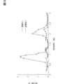
次に、図10および図11に基づき、アイランド223による効果を説明する。図10、図11は、電磁界シミュレーションの結果を示す電界強度分布図である。電磁界シミュレーションは、光伝送モジュールの解析モデルに対し有限要素法を用いて、光コネクタの開口側から遠方界を想定した平行な平面波を入射し、GHzオーダーの通信周波数帯を想定した条件にて行った。図10は、参考例の結果を示している。参考例では、プリント基板に上記したアイランドを設けず、嵌合部の直下にもグランドパターンを設けた。図10では、本実施形態の要素と同一または関連する要素について、本実施形態の符号の末尾にrを付け加えて示している。図11は、本実施形態に記載した構成、すなわち図4に示したように、嵌合部312の直下にアイランド223を設けた構成の結果を示している。Next, the effect of the
図10、図11に示すように、アイランド223を設けたほうが、アイランドなしの構成よりも、電界強度が低い。よって、嵌合部312の直下にアイランド223を設けると、アイランド223を設けない構成よりも電磁波ノイズの影響を受けにくいことが明らかである。アイランド223をグランドパターン220から分離することで、プリント基板20内のノイズループ電流がアイランド223で分断されるため、プリント基板20の共振周波数が高域側にシフトし、電磁波ノイズの影響を受けにくくなると考えられる。As shown in Figures 10 and 11, the electric field strength is lower when the
なお、図示を省略するが、光電変換部周辺についても同様に電磁界シミュレーションを行った。アイランドを設けない参考例の場合、COBモジュールを構成する基板、光電変換素子、および回路チップの周辺において電界強度が高くなり、アイランド223を設けた構成では、同箇所の電界強度を低くなった。この点からも、電磁波ノイズによる光電変換部40の誤動作を抑制できることが明らかとなった。Although not shown in the figure, a similar electromagnetic field simulation was also performed around the photoelectric conversion unit. In the reference example where no island was provided, the electric field strength was high around the substrate, photoelectric conversion element, and circuit chip that constitute the COB module, while in the configuration where
上記したように、シールド部材50は、端子部32および光電変換部40を取り囲むように配置され、グランドパターン220とは電気的に分離されていればよい。シールド部材50をひとつの部材のみにより構成してもよい。たとえば、外部シールド51のみを有する構成としてもよい。As described above, the shielding
本実施形態のシールド部材50は、外部シールド51に加えて、内部シールド52を有している。これにより、外部コネクタ17を接続するための開口部51aを有する構成において、開口部51aから侵入した電磁波ノイズが光電変換部40に影響を及ぼすのを抑制することができる。The shielding
図12~図15は、外部シールド51と内部シールド52との電気的な接続の有無による電磁波ノイズの影響を示す図である。図中において、導通なしが電気的に分離を示し、導通ありが電気的に接続を示している。図12~図15は、電磁波ノイズによって異なるパターン間に生じる電圧を示すシミュレーション結果である。シミュレーションは、光伝送モジュールの解析モデルに対し有限要素法を用いて、光コネクタの開口側から遠方界を想定した平行な平面波を入射し、GHzオーダーの通信周波数帯を想定した条件にて行った。図12、図13は、プリント基板の結果を示している。図12は、電源パターンとグランドパターンの間の電圧を示し、図13は、シグナルパターンとグランドパターンの間の電圧を示している。図14、図15は、COBモジュールの基板の結果を示している。図14は、電源パターンとグランドパターンの間の電圧を示し、図15は、シグナルパターンとグランドパターンの間の電圧を示している。Figures 12 to 15 are diagrams showing the influence of electromagnetic noise depending on the presence or absence of electrical connection between the
外部シールド51と内部シールド52とは、電気的に分離するのが好ましい。電気的な分離により、外部シールド51から内部シールド52へのノイズの回り込みを抑制することができる。図12~図15に示すシミュレーション結果からも、広い周波数域において電磁波ノイズの伝搬を抑制できることが明らかである。図12~図15に示すように、一部の周波数においては、外部シールド51と内部シールド52とを電気的に接続したほうが、電磁波ノイズを抑制することができる。よって、外部シールド51と内部シールド52とを、電気的に接続してもよい。It is preferable to electrically separate the
外部シールド51は、アイランド223に対して電気的に接続されてもよい。本実施形態の構成によれば、ばね部51cの弾性変形の反力により、外部シールド51がペグ33に電気的に接続されている。また、ペグ33が、はんだ等の導電性接合材を介して、アイランド223に接続されている。よって、外部シールド51とアイランド223との電気的な接続を、簡素な構成で実現できる。電気的な接続によりアイランド223も電磁波シールドとして機能させつつ、グランドパターン220との分離により電磁波ノイズの伝搬を抑制することができる。The
外部シールド51は、アイランド223に対して電気的に分離されてもよい。上記構成において、たとえば非導電性の接着材を用いてペグ33をアイランド223に固定することで、外部シールド51とアイランド223とを絶縁分離することができる。ペグ33と外部シールド51との固定部において絶縁分離してもよい。The
外部シールド51をペグ33に固定する例を示したが、これに限定されない。外部シールド51を、接着等によってハウジング31に固定してもよい。この構成でも、外部シールド51をアイランド223に対して電気的に分離することができる。Although an example in which the
(第2実施形態)
この実施形態は、先行する実施形態を基礎的形態とする変形例であり、先行実施形態の記載を援用できる。先行実施形態では、シールド部材が、光伝送モジュールの外部の金属部材に対して、電気的に接続されていなかった。これに代えて、シールド部材をフレームグランドに接続してもよい。 Second Embodiment
This embodiment is a modification based on the previous embodiment, and the description of the previous embodiment can be used. In the previous embodiment, the shielding member is not electrically connected to the metal member outside the optical transmission module. Instead, the shielding member may be connected to the frame ground.
図16は、本実施形態に係る光伝送モジュール12および電子制御装置10を示す断面図である。電子制御装置10は、金属筐体18を備えている。金属筐体18は、複数の部材18A、18Bを相互に組み付けること構成されている。電子制御装置10、金属筐体18内に、上記した電源回路13、制御回路14、通信回路15、16、コネクタ11の少なくとも一部、光伝送モジュール12の少なくとも一部、を収容している。図16に示す例では、光伝送モジュール12の全体を収容している。金属筐体18は、外部機器との接続のために、コネクタ11および光伝送モジュール12用の開口部をそれぞれ有している。Figure 16 is a cross-sectional view showing the
金属筐体18は、光伝送モジュール12用の開口部の周辺部位として、フィンガばね等のばね部を有している。複数の部材18A、18Bを組み付ける際に、ばね部は、光伝送モジュール12の外部シールド51に接触して弾性変形する。Z方向両側からのばね部による押圧で、外部シールド51と金属筐体18との電気的な接続が確保されている。The
<第2実施形態のまとめ>
本実施形態によれば、光伝送モジュール12の外部シールド51が、電子制御装置10の金属筐体18に電気的に接続されている。これにより、電磁波ノイズを、外部シールド51から金属筐体18に逃がすことができる。よって、電磁波ノイズによる光電変換部40の誤動作を抑制することができる。金属筐体18がフレームグランドに相当する。 <Summary of the Second Embodiment>
According to the present embodiment, the
金属筐体18がフレームグランドとして機能する例を示したが、これに限定されない。シールド部材50の少なくとも外部シールド51を、車両のシャーシグランドに電気的に接続してもよい。シャーシグランドもフレームグランドとして機能する。An example has been shown in which the
(他の実施形態)
この明細書および図面等における開示は、例示された実施形態に制限されない。開示は、例示された実施形態と、それらに基づく当業者による変形態様を包含する。たとえば、開示は、実施形態において示された部品および/または要素の組み合わせに限定されない。開示は、多様な組み合わせによって実施可能である。開示は、実施形態に追加可能な追加的な部分をもつことができる。開示は、実施形態の部品および/または要素が省略されたものを包含する。開示は、ひとつの実施形態と他の実施形態との間における部品および/または要素の置き換え、または組み合わせを包含する。開示される技術的範囲は、実施形態の記載に限定されない。開示されるいくつかの技術的範囲は、請求の範囲の記載によって示され、さらに請求の範囲の記載と均等の意味および範囲内でのすべての変更を含むものと解されるべきである。 Other Embodiments
The disclosure in this specification and drawings, etc. is not limited to the exemplified embodiments. The disclosure includes the exemplified embodiments and modifications by those skilled in the art based thereon. For example, the disclosure is not limited to the combination of parts and/or elements shown in the embodiments. The disclosure can be implemented by various combinations. The disclosure can have additional parts that can be added to the embodiments. The disclosure includes the omission of parts and/or elements of the embodiments. The disclosure includes the replacement or combination of parts and/or elements between one embodiment and another embodiment. The disclosed technical scope is not limited to the description of the embodiments. Some disclosed technical scopes are indicated by the description of the claims, and should be interpreted as including all modifications within the meaning and scope equivalent to the description of the claims.
明細書および図面等における開示は、請求の範囲の記載によって限定されない。明細書および図面等における開示は、請求の範囲に記載された技術的思想を包含し、さらに請求の範囲に記載された技術的思想より多様で広範な技術的思想に及んでいる。よって、請求の範囲の記載に拘束されることなく、明細書および図面等の開示から、多様な技術的思想を抽出することができる。The disclosure in the specification and drawings, etc. is not limited by the claims. The disclosure in the specification and drawings, etc. encompasses the technical ideas described in the claims, and extends to more diverse and extensive technical ideas than the technical ideas described in the claims. Therefore, various technical ideas can be extracted from the disclosure in the specification and drawings, etc., without being bound by the claims.
ある要素または層が「上にある」、「連結されている」、「接続されている」または「結合されている」と言及されている場合、それは、他の要素、または他の層に対して、直接的に上に、連結され、接続され、または結合されていることがあり、さらに、介在要素または介在層が存在していることがある。対照的に、ある要素が別の要素または層に「直接的に上に」、「直接的に連結されている」、「直接的に接続されている」または「直接的に結合されている」と言及されている場合、介在要素または介在層は存在しない。要素間の関係を説明するために使用される他の言葉は、同様のやり方で(例えば、「間に」対「直接的に間に」、「隣接する」対「直接的に隣接する」など)解釈されるべきである。この明細書で使用される場合、用語「および/または」は、関連する列挙された1つまたは複数の項目に関する任意の組み合わせ、およびすべての組み合わせを含む。When an element or layer is referred to as being "on," "coupled," "connected," or "bonded," it may be directly coupled, connected, or bonded to another element or layer, and intervening elements or layers may be present. In contrast, when an element is referred to as being "directly on," "directly coupled," "directly connected," or "directly bonded" to another element or layer, no intervening elements or layers are present. Other words used to describe relationships between elements should be construed in a similar manner (e.g., "between" vs. "directly between," "adjacent" vs. "directly adjacent," etc.). As used in this specification, the term "and/or" includes any and all combinations of one or more associated listed items.
空間的に相対的な用語「内」、「外」、「裏」、「下」、「低」、「上」、「高」などは、図示されているような、ひとつの要素または特徴の他の要素または特徴に対する関係を説明する記載を容易にするためにここでは利用されている。空間的に相対的な用語は、図面に描かれている向きに加えて、使用または操作中の装置の異なる向きを包含することを意図することができる。例えば、図中の装置をひっくり返すと、他の要素または特徴の「下」または「真下」として説明されている要素は、他の要素または特徴の「上」に向けられる。したがって、用語「下」は、上と下の両方の向きを包含することができる。この装置は、他の方向に向いていてもよく(90度または他の向きに回転されてもよい)、この明細書で使用される空間的に相対的な記述子はそれに応じて解釈される。Spatially relative terms such as "inside," "outside," "back," "bottom," "low," "top," "top," and the like are utilized herein for ease of description to describe the relationship of one element or feature to other elements or features as depicted in the figures. Spatially relative terms may be intended to encompass different orientations of the device during use or operation in addition to the orientation depicted in the figures. For example, if the device in the figures is turned over, elements described as "below" or "directly below" other elements or features would be oriented "above" the other elements or features. Thus, the term "bottom" can encompass both an orientation of top and bottom. The device may be otherwise oriented (rotated 90 degrees or at other orientations) and the spatially relative descriptors used in this specification would be interpreted accordingly.
制御回路14は、少なくともひとつのコンピュータを含む制御システムによって提供される。制御システムは、ハードウェアである少なくともひとつのプロセッサ(ハードウェアプロセッサ)を含む。ハードウェアプロセッサは、下記(i)、(ii)、または(iii)により提供することができる。The
(i)ハードウェアプロセッサは、ハードウェア論理回路である場合がある。この場合、コンピュータは、プログラムされた多数の論理ユニット(ゲート回路)を含むデジタル回路によって提供される。デジタル回路は、プログラムおよび/またはデータを格納したメモリを備える場合がある。コンピュータは、アナログ回路によって提供される場合がある。コンピュータは、デジタル回路とアナログ回路との組み合わせによって提供される場合がある。(i) A hardware processor may be a hardware logic circuit. In this case, the computer is provided by digital circuits that include a large number of programmed logic units (gate circuits). The digital circuits may include memory that stores programs and/or data. The computer may be provided by analog circuits. The computer may be provided by a combination of digital and analog circuits.
(ii)ハードウェアプロセッサは、少なくともひとつのメモリに格納されたプログラムを実行する少なくともひとつのプロセッサコアである場合がある。この場合、コンピュータは、少なくともひとつのメモリと、少なくともひとつのプロセッサコアとによって提供される。プロセッサコアは、たとえばCPUと称される。メモリは、記憶媒体とも称される。メモリは、プロセッサによって読み取り可能な「プログラムおよび/またはデータ」を非一時的に格納する非遷移的かつ実体的な記憶媒体である。(ii) The hardware processor may be at least one processor core that executes a program stored in at least one memory. In this case, the computer is provided with at least one memory and at least one processor core. The processor core is referred to as a CPU, for example. The memory is also referred to as a storage medium. The memory is a non-transient and tangible storage medium that non-transiently stores "programs and/or data" that can be read by the processor.
(iii)ハードウェアプロセッサは、上記(i)と上記(ii)との組み合わせである場合がある。(i)と(ii)とは、異なるチップの上、または共通のチップの上に配置される。(iii) The hardware processor may be a combination of (i) and (ii) above, where (i) and (ii) are located on different chips or on a common chip.
すなわち、制御回路14が提供する手段および/または機能は、ハードウェアのみ、ソフトウェアのみ、またはそれらの組み合わせにより提供することができる。That is, the means and/or functions provided by the
ハウジング31および外部シールド51が、外部コネクタ17との嵌合のためにX方向において開口する例を示したが、これに限定されない。これら開口は、プリント基板20側の面、すなわちプリント基板20と対向する下面、とは異なる面に設けられればよい。たとえば、プリント基板20と対向する下面とは反対の面、すなわち上面に開口を設けてもよい。An example has been shown in which the
1、3…ワイヤハーネス、2…バッテリ、4、6…外部機器、5…光ファイバケーブル、10…電子制御装置、11…コネクタ、12…光伝送モジュール、13…電源回路、14…制御回路、15、16…通信回路、17…外部コネクタ、170…ハウジング、171…フェルール、18…金属筐体(フレームグランド)、20…プリント基板、20a…一端、21…絶縁基材、22…導体パターン、220…グランドパターン、221…シグナルパターン、222…パッド、222a…シグナルパッド、222b…グランドパッド、222c…電源パッド、223…アイランド、23…接続ビア、24…溝、30…光コネクタ、31…ハウジング、310…筒部、310a…開口部、311…隔壁、311a…貫通孔、312…嵌合部、313…収容部、32…端子部、320…フェルール、321…光ファイバ、322…スリーブ、33…ペグ、330…係止孔、40…光電変換部、41…基板、410…絶縁基材、411…導体パターン、42…光電変換素子、43…回路チップ、44…リード端子、45…ボンディングワイヤ、46…絶縁性パッケージ、50…シールド部材、51…外部シールド、51a…開口部、51b…係止突起、51c…ばね部、52…内部シールド、520…カバー、521…リッド、521a…筒部、522…係止突起1, 3...wire harness, 2...battery, 4, 6...external device, 5...optical fiber cable, 10...electronic control device, 11...connector, 12...optical transmission module, 13...power supply circuit, 14...control circuit, 15, 16...communication circuit, 17...external connector, 170...housing, 171...ferrule, 18...metal housing (frame ground), 20...printed circuit board, 20a...one end, 21...insulating substrate, 22...conductor pattern, 220...ground pattern, 221...signal pattern, 222...pad, 222a...signal pad, 222b...ground pad, 222c...power supply pad, 223...island, 23...connection via, 24...groove, 30...optical connector , 31...housing, 310...tubular portion, 310a...opening, 311...partition wall, 311a...through hole, 312...fitting portion, 313...accommodating portion, 32...terminal portion, 320...ferrule, 321...optical fiber, 322...sleeve, 33...peg, 330...locking hole, 40...photoelectric conversion portion, 41...substrate, 410...insulating substrate, 411...conductor pattern, 42...photoelectric conversion element, 43...circuit chip, 44...lead terminal, 45...bonding wire, 46...insulating package, 50...shield member, 51...external shield, 51a...opening, 51b...locking protrusion, 51c...spring portion, 52...internal shield, 520...cover, 521...lid, 521a...tubular portion, 522...locking protrusion
Claims (8)
Translated fromJapanese前記プリント基板に実装されており、開口(310a)を通じて外部コネクタ(17)が嵌合する嵌合部(312)を備えたハウジング(31)と、前記ハウジングに収容されており、前記外部コネクタが光学的に結合する端子部(32)と、を有する光コネクタ(30)と、
前記端子部に光学的に結合された光電変換素子(42)と、前記光電変換素子および前記グランドパターンのそれぞれに電気的に接続された回路部(41、43)を有し、前記開口に対して前記端子部よりも奥側で前記ハウジングに収容された光電変換部(40)と、
電磁遮蔽性を有し、前記端子部および前記光電変換部を取り囲むように配置されたシールド部材(50)と、
を備え、
前記シールド部材は、前記グランドパターンとは電気的に分離されており、
前記プリント基板は、前記導体パターンとして、前記プリント基板の板厚方向からの平面視において前記嵌合部と重なる位置に、前記グランドパターンとは電気的に分離されたアイランド(223)を有している光伝送モジュール。 A printed circuit board (20) having a conductor pattern (22) including a ground pattern (220);
an optical connector (30) including a housing (31) mounted on the printed circuit board and having a fitting portion (312) into which an external connector (17) fits through an opening (310a), and a terminal portion (32) accommodated in the housing and optically coupled to the external connector;
a photoelectric conversion unit (40) that has a photoelectric conversion element (42) optically coupled to the terminal portion, and a circuit portion (41, 43) electrically connected to the photoelectric conversion element and the ground pattern, and is accommodated in the housing on a deeper side than the terminal portion with respect to the opening;
a shielding member (50) having electromagnetic shielding properties and arranged to surround the terminal portion and the photoelectric conversion portion;
Equipped with
the shielding member is electrically isolated from the ground pattern,
The printed circuit board has, as the conductor pattern, an island (223) electrically isolated from the ground pattern at a position overlapping with the mating portion when viewed in a plan view from the thickness direction of the printed circuit board.
前記光伝送モジュールを介して外部機器(6)と光通信可能に接続される制御回路(14)と、
を備える電子制御装置。 The optical transmission module (12) according to any one of claims 1 to 7;
a control circuit (14) connected to an external device (6) via the optical transmission module so as to be capable of optical communication;
An electronic control device comprising:
Priority Applications (2)
| Application Number | Priority Date | Filing Date | Title |
|---|---|---|---|
| JP2020102498AJP7466386B2 (en) | 2020-06-12 | 2020-06-12 | Optical transmission module and electronic control device |
| DE102021114693.3ADE102021114693B4 (en) | 2020-06-12 | 2021-06-08 | OPTICAL TRANSMISSION MODULE AND ELECTRONIC CONTROL UNIT |
Applications Claiming Priority (1)
| Application Number | Priority Date | Filing Date | Title |
|---|---|---|---|
| JP2020102498AJP7466386B2 (en) | 2020-06-12 | 2020-06-12 | Optical transmission module and electronic control device |
Publications (2)
| Publication Number | Publication Date |
|---|---|
| JP2021197435A JP2021197435A (en) | 2021-12-27 |
| JP7466386B2true JP7466386B2 (en) | 2024-04-12 |
Family
ID=78718893
Family Applications (1)
| Application Number | Title | Priority Date | Filing Date |
|---|---|---|---|
| JP2020102498AActiveJP7466386B2 (en) | 2020-06-12 | 2020-06-12 | Optical transmission module and electronic control device |
Country Status (2)
| Country | Link |
|---|---|
| JP (1) | JP7466386B2 (en) |
| DE (1) | DE102021114693B4 (en) |
Citations (7)
| Publication number | Priority date | Publication date | Assignee | Title |
|---|---|---|---|---|
| JP2001298239A (en) | 2000-02-10 | 2001-10-26 | Sumitomo Electric Ind Ltd | Optical communication module and method for manufacturing optical communication module |
| US20020110336A1 (en) | 2001-02-12 | 2002-08-15 | Edwin Dair | Fiber-optic modules with housing/shielding |
| CN2552022Y (en) | 2001-11-03 | 2003-05-21 | 富士康(昆山)电脑接插件有限公司 | Small plug-type light emitting/receiving module |
| JP2003264471A (en) | 2002-03-06 | 2003-09-19 | Sharp Corp | Optical transceiver circuit board and optical transceiver module |
| JP2014025981A (en) | 2012-07-24 | 2014-02-06 | Auto Network Gijutsu Kenkyusho:Kk | Optical connector with lid |
| JP2014038303A (en) | 2012-07-19 | 2014-02-27 | Yazaki Corp | Optical connector and fitting unit |
| JP2020512544A (en) | 2017-03-01 | 2020-04-23 | アウスター インコーポレイテッド | Accurate photodetector measurements for lidar |
Family Cites Families (4)
| Publication number | Priority date | Publication date | Assignee | Title |
|---|---|---|---|---|
| JP2666142B2 (en) | 1987-02-04 | 1997-10-22 | 旭光学工業株式会社 | Automatic focus detection device for camera |
| JP2559423B2 (en) | 1987-09-14 | 1996-12-04 | 株式会社日立製作所 | Backlight device for liquid crystal display |
| JP3409530B2 (en)* | 1995-09-01 | 2003-05-26 | 住友電装株式会社 | How to fix optical fiber connectors |
| JP4325177B2 (en) | 2002-11-18 | 2009-09-02 | 富士ゼロックス株式会社 | Optical transmission module |
- 2020
- 2020-06-12JPJP2020102498Apatent/JP7466386B2/enactiveActive
- 2021
- 2021-06-08DEDE102021114693.3Apatent/DE102021114693B4/enactiveActive
Patent Citations (7)
| Publication number | Priority date | Publication date | Assignee | Title |
|---|---|---|---|---|
| JP2001298239A (en) | 2000-02-10 | 2001-10-26 | Sumitomo Electric Ind Ltd | Optical communication module and method for manufacturing optical communication module |
| US20020110336A1 (en) | 2001-02-12 | 2002-08-15 | Edwin Dair | Fiber-optic modules with housing/shielding |
| CN2552022Y (en) | 2001-11-03 | 2003-05-21 | 富士康(昆山)电脑接插件有限公司 | Small plug-type light emitting/receiving module |
| JP2003264471A (en) | 2002-03-06 | 2003-09-19 | Sharp Corp | Optical transceiver circuit board and optical transceiver module |
| JP2014038303A (en) | 2012-07-19 | 2014-02-27 | Yazaki Corp | Optical connector and fitting unit |
| JP2014025981A (en) | 2012-07-24 | 2014-02-06 | Auto Network Gijutsu Kenkyusho:Kk | Optical connector with lid |
| JP2020512544A (en) | 2017-03-01 | 2020-04-23 | アウスター インコーポレイテッド | Accurate photodetector measurements for lidar |
Also Published As
| Publication number | Publication date |
|---|---|
| DE102021114693A1 (en) | 2021-12-16 |
| JP2021197435A (en) | 2021-12-27 |
| DE102021114693B4 (en) | 2025-01-23 |
Similar Documents
| Publication | Publication Date | Title |
|---|---|---|
| KR100486474B1 (en) | Connector | |
| EP3745702B1 (en) | Camera module | |
| JP2025124910A (en) | Circuit board fixing device for camera module and camera module | |
| JP4851462B2 (en) | Optical and electrical composite connector | |
| JP3059223B2 (en) | Controllers especially for automobiles | |
| JP7557830B2 (en) | Connector and mating connector | |
| JP7588365B2 (en) | Connector device, connector and mating connector | |
| JP2025003688A (en) | Connector and Mating Connector | |
| JP2021190375A (en) | Shield member, shield unit, and connector module | |
| WO2011008727A1 (en) | Optical connector | |
| WO2011008729A2 (en) | Optical connector | |
| JP7707079B2 (en) | Camera module and method for manufacturing the camera module | |
| JP2019062114A (en) | Optical receiver module package | |
| EP4236337A2 (en) | Electronic equipment, imaging device, and mobile body | |
| JP7466386B2 (en) | Optical transmission module and electronic control device | |
| KR20230020308A (en) | Camera module | |
| US7186037B2 (en) | Optical active connector | |
| KR20240130343A (en) | Tile-shaped transmit/receive module device of phased array radar | |
| JP4325177B2 (en) | Optical transmission module | |
| US10942226B2 (en) | Cable with resin compact | |
| JP6216902B2 (en) | Optical module | |
| JP2016020937A (en) | Photoelectric conversion device and signal transmission device using the same | |
| US20240272540A1 (en) | Vehicular camera | |
| JP6661733B1 (en) | Cable and image transmission system | |
| KR20220166600A (en) | Camera module |
Legal Events
| Date | Code | Title | Description |
|---|---|---|---|
| A621 | Written request for application examination | Free format text:JAPANESE INTERMEDIATE CODE: A621 Effective date:20230410 | |
| A977 | Report on retrieval | Free format text:JAPANESE INTERMEDIATE CODE: A971007 Effective date:20240301 | |
| TRDD | Decision of grant or rejection written | ||
| A01 | Written decision to grant a patent or to grant a registration (utility model) | Free format text:JAPANESE INTERMEDIATE CODE: A01 Effective date:20240305 | |
| A61 | First payment of annual fees (during grant procedure) | Free format text:JAPANESE INTERMEDIATE CODE: A61 Effective date:20240402 | |
| R150 | Certificate of patent or registration of utility model | Ref document number:7466386 Country of ref document:JP Free format text:JAPANESE INTERMEDIATE CODE: R150 |