JP7465771B2 - Compound sintered body, semiconductor manufacturing equipment member, and method for manufacturing compound sintered body - Google Patents
Compound sintered body, semiconductor manufacturing equipment member, and method for manufacturing compound sintered bodyDownload PDFInfo
- Publication number
- JP7465771B2 JP7465771B2JP2020154641AJP2020154641AJP7465771B2JP 7465771 B2JP7465771 B2JP 7465771B2JP 2020154641 AJP2020154641 AJP 2020154641AJP 2020154641 AJP2020154641 AJP 2020154641AJP 7465771 B2JP7465771 B2JP 7465771B2
- Authority
- JP
- Japan
- Prior art keywords
- electrode
- sintered body
- zro2
- difference
- less
- Prior art date
- Legal status (The legal status is an assumption and is not a legal conclusion. Google has not performed a legal analysis and makes no representation as to the accuracy of the status listed.)
- Active
Links
- 150000001875compoundsChemical class0.000titleclaimsdescription50
- 238000004519manufacturing processMethods0.000titleclaimsdescription49
- 239000004065semiconductorSubstances0.000titleclaimsdescription29
- 238000000034methodMethods0.000titleclaimsdescription20
- 239000000758substrateSubstances0.000claimsdescription50
- 239000000463materialSubstances0.000claimsdescription47
- 238000005245sinteringMethods0.000claimsdescription28
- 239000002131composite materialSubstances0.000claimsdescription20
- RVTZCBVAJQQJTK-UHFFFAOYSA-Noxygen(2-);zirconium(4+)Chemical compound[O-2].[O-2].[Zr+4]RVTZCBVAJQQJTK-UHFFFAOYSA-N0.000claimsdescription15
- 229910001928zirconium oxideInorganic materials0.000claimsdescription15
- WFKWXMTUELFFGS-UHFFFAOYSA-NtungstenChemical group[W]WFKWXMTUELFFGS-UHFFFAOYSA-N0.000claimsdescription13
- 239000010937tungstenSubstances0.000claimsdescription13
- 239000000919ceramicSubstances0.000claimsdescription12
- 238000002441X-ray diffractionMethods0.000claimsdescription11
- 229910052721tungstenInorganic materials0.000claimsdescription10
- 239000002243precursorSubstances0.000claimsdescription6
- TWNQGVIAIRXVLR-UHFFFAOYSA-Noxo(oxoalumanyloxy)alumaneChemical groupO=[Al]O[Al]=OTWNQGVIAIRXVLR-UHFFFAOYSA-N0.000claimsdescription5
- 229910001930tungsten oxideInorganic materials0.000claimsdescription5
- 238000010030laminatingMethods0.000claimsdescription2
- MCMNRKCIXSYSNV-UHFFFAOYSA-NZirconium dioxideChemical compoundO=[Zr]=OMCMNRKCIXSYSNV-UHFFFAOYSA-N0.000description213
- 239000002994raw materialSubstances0.000description35
- 239000000843powderSubstances0.000description30
- 230000000052comparative effectEffects0.000description28
- 239000000203mixtureSubstances0.000description21
- 238000010304firingMethods0.000description20
- 229910018072Al 2 O 3Inorganic materials0.000description18
- PNEYBMLMFCGWSK-UHFFFAOYSA-Naluminium oxideInorganic materials[O-2].[O-2].[O-2].[Al+3].[Al+3]PNEYBMLMFCGWSK-UHFFFAOYSA-N0.000description18
- CPLXHLVBOLITMK-UHFFFAOYSA-Nmagnesium oxideInorganic materials[Mg]=OCPLXHLVBOLITMK-UHFFFAOYSA-N0.000description14
- 239000000395magnesium oxideSubstances0.000description14
- AXZKOIWUVFPNLO-UHFFFAOYSA-Nmagnesium;oxygen(2-)Chemical compound[O-2].[Mg+2]AXZKOIWUVFPNLO-UHFFFAOYSA-N0.000description14
- 239000002003electrode pasteSubstances0.000description13
- 238000002156mixingMethods0.000description11
- 239000002245particleSubstances0.000description11
- 239000002904solventSubstances0.000description10
- 238000007731hot pressingMethods0.000description9
- 229910052593corundumInorganic materials0.000description7
- 229910001845yogo sapphireInorganic materials0.000description7
- 229910020068MgAlInorganic materials0.000description6
- 229910019092Mg-OInorganic materials0.000description5
- 229910019395Mg—OInorganic materials0.000description5
- 239000003960organic solventSubstances0.000description5
- 239000000654additiveSubstances0.000description4
- 230000000996additive effectEffects0.000description4
- 239000011230binding agentSubstances0.000description4
- 238000002844meltingMethods0.000description4
- 230000008018meltingEffects0.000description4
- 238000000465mouldingMethods0.000description4
- IJGRMHOSHXDMSA-UHFFFAOYSA-NAtomic nitrogenChemical compoundN#NIJGRMHOSHXDMSA-UHFFFAOYSA-N0.000description3
- 229910001873dinitrogenInorganic materials0.000description3
- 239000006185dispersionSubstances0.000description3
- -1mixing timeSubstances0.000description3
- 230000003647oxidationEffects0.000description3
- 238000007254oxidation reactionMethods0.000description3
- 238000007650screen-printingMethods0.000description3
- 238000003826uniaxial pressingMethods0.000description3
- OKTJSMMVPCPJKN-UHFFFAOYSA-NCarbonChemical compound[C]OKTJSMMVPCPJKN-UHFFFAOYSA-N0.000description2
- 238000003763carbonizationMethods0.000description2
- 238000007580dry-mixingMethods0.000description2
- 238000005516engineering processMethods0.000description2
- 238000011049fillingMethods0.000description2
- 239000007789gasSubstances0.000description2
- 229910002804graphiteInorganic materials0.000description2
- 239000010439graphiteSubstances0.000description2
- 238000010438heat treatmentMethods0.000description2
- 229910001635magnesium fluorideInorganic materials0.000description2
- 239000000696magnetic materialSubstances0.000description2
- 238000005259measurementMethods0.000description2
- 238000003825pressingMethods0.000description2
- 238000001878scanning electron micrographMethods0.000description2
- 239000002002slurrySubstances0.000description2
- UONOETXJSWQNOL-UHFFFAOYSA-Ntungsten carbideChemical compound[W+]#[C-]UONOETXJSWQNOL-UHFFFAOYSA-N0.000description2
- XLYOFNOQVPJJNP-UHFFFAOYSA-NwaterSubstancesOXLYOFNOQVPJJNP-UHFFFAOYSA-N0.000description2
- OAYXUHPQHDHDDZ-UHFFFAOYSA-N2-(2-butoxyethoxy)ethanolChemical compoundCCCCOCCOCCOOAYXUHPQHDHDDZ-UHFFFAOYSA-N0.000description1
- 230000002411adverseEffects0.000description1
- SNAAJJQQZSMGQD-UHFFFAOYSA-Naluminum magnesiumChemical compound[Mg].[Al]SNAAJJQQZSMGQD-UHFFFAOYSA-N0.000description1
- 238000006243chemical reactionMethods0.000description1
- 239000013078crystalSubstances0.000description1
- 230000003247decreasing effectEffects0.000description1
- 238000010586diagramMethods0.000description1
- 238000009826distributionMethods0.000description1
- 230000000694effectsEffects0.000description1
- 239000007772electrode materialSubstances0.000description1
- 238000005530etchingMethods0.000description1
- 239000012530fluidSubstances0.000description1
- 230000005764inhibitory processEffects0.000description1
- 238000003475laminationMethods0.000description1
- 239000011268mixed slurrySubstances0.000description1
- 238000012986modificationMethods0.000description1
- 230000004048modificationEffects0.000description1
- 230000003287optical effectEffects0.000description1
- 230000001590oxidative effectEffects0.000description1
- 229920001490poly(butyl methacrylate) polymerPolymers0.000description1
- 239000011148porous materialSubstances0.000description1
- 239000007787solidSubstances0.000description1
- 238000001179sorption measurementMethods0.000description1
- 229910052596spinelInorganic materials0.000description1
- 239000011029spinelSubstances0.000description1
- 230000001629suppressionEffects0.000description1
Images

Classifications
- C—CHEMISTRY; METALLURGY
- C04—CEMENTS; CONCRETE; ARTIFICIAL STONE; CERAMICS; REFRACTORIES
- C04B—LIME, MAGNESIA; SLAG; CEMENTS; COMPOSITIONS THEREOF, e.g. MORTARS, CONCRETE OR LIKE BUILDING MATERIALS; ARTIFICIAL STONE; CERAMICS; REFRACTORIES; TREATMENT OF NATURAL STONE
- C04B35/00—Shaped ceramic products characterised by their composition; Ceramics compositions; Processing powders of inorganic compounds preparatory to the manufacturing of ceramic products
- C04B35/01—Shaped ceramic products characterised by their composition; Ceramics compositions; Processing powders of inorganic compounds preparatory to the manufacturing of ceramic products based on oxide ceramics
- C04B35/10—Shaped ceramic products characterised by their composition; Ceramics compositions; Processing powders of inorganic compounds preparatory to the manufacturing of ceramic products based on oxide ceramics based on aluminium oxide
- C04B35/111—Fine ceramics
- C04B35/117—Composites
- C04B35/119—Composites with zirconium oxide
- C—CHEMISTRY; METALLURGY
- C04—CEMENTS; CONCRETE; ARTIFICIAL STONE; CERAMICS; REFRACTORIES
- C04B—LIME, MAGNESIA; SLAG; CEMENTS; COMPOSITIONS THEREOF, e.g. MORTARS, CONCRETE OR LIKE BUILDING MATERIALS; ARTIFICIAL STONE; CERAMICS; REFRACTORIES; TREATMENT OF NATURAL STONE
- C04B37/00—Joining burned ceramic articles with other burned ceramic articles or other articles by heating
- C04B37/003—Joining burned ceramic articles with other burned ceramic articles or other articles by heating by means of an interlayer consisting of a combination of materials selected from glass, or ceramic material with metals, metal oxides or metal salts
- C04B37/006—Joining burned ceramic articles with other burned ceramic articles or other articles by heating by means of an interlayer consisting of a combination of materials selected from glass, or ceramic material with metals, metal oxides or metal salts consisting of metals or metal salts
- C—CHEMISTRY; METALLURGY
- C04—CEMENTS; CONCRETE; ARTIFICIAL STONE; CERAMICS; REFRACTORIES
- C04B—LIME, MAGNESIA; SLAG; CEMENTS; COMPOSITIONS THEREOF, e.g. MORTARS, CONCRETE OR LIKE BUILDING MATERIALS; ARTIFICIAL STONE; CERAMICS; REFRACTORIES; TREATMENT OF NATURAL STONE
- C04B35/00—Shaped ceramic products characterised by their composition; Ceramics compositions; Processing powders of inorganic compounds preparatory to the manufacturing of ceramic products
- C04B35/01—Shaped ceramic products characterised by their composition; Ceramics compositions; Processing powders of inorganic compounds preparatory to the manufacturing of ceramic products based on oxide ceramics
- C04B35/10—Shaped ceramic products characterised by their composition; Ceramics compositions; Processing powders of inorganic compounds preparatory to the manufacturing of ceramic products based on oxide ceramics based on aluminium oxide
- C04B35/111—Fine ceramics
- B—PERFORMING OPERATIONS; TRANSPORTING
- B32—LAYERED PRODUCTS
- B32B—LAYERED PRODUCTS, i.e. PRODUCTS BUILT-UP OF STRATA OF FLAT OR NON-FLAT, e.g. CELLULAR OR HONEYCOMB, FORM
- B32B18/00—Layered products essentially comprising ceramics, e.g. refractory products
- C—CHEMISTRY; METALLURGY
- C04—CEMENTS; CONCRETE; ARTIFICIAL STONE; CERAMICS; REFRACTORIES
- C04B—LIME, MAGNESIA; SLAG; CEMENTS; COMPOSITIONS THEREOF, e.g. MORTARS, CONCRETE OR LIKE BUILDING MATERIALS; ARTIFICIAL STONE; CERAMICS; REFRACTORIES; TREATMENT OF NATURAL STONE
- C04B35/00—Shaped ceramic products characterised by their composition; Ceramics compositions; Processing powders of inorganic compounds preparatory to the manufacturing of ceramic products
- C04B35/01—Shaped ceramic products characterised by their composition; Ceramics compositions; Processing powders of inorganic compounds preparatory to the manufacturing of ceramic products based on oxide ceramics
- C04B35/10—Shaped ceramic products characterised by their composition; Ceramics compositions; Processing powders of inorganic compounds preparatory to the manufacturing of ceramic products based on oxide ceramics based on aluminium oxide
- C04B35/111—Fine ceramics
- C04B35/117—Composites
- C—CHEMISTRY; METALLURGY
- C04—CEMENTS; CONCRETE; ARTIFICIAL STONE; CERAMICS; REFRACTORIES
- C04B—LIME, MAGNESIA; SLAG; CEMENTS; COMPOSITIONS THEREOF, e.g. MORTARS, CONCRETE OR LIKE BUILDING MATERIALS; ARTIFICIAL STONE; CERAMICS; REFRACTORIES; TREATMENT OF NATURAL STONE
- C04B35/00—Shaped ceramic products characterised by their composition; Ceramics compositions; Processing powders of inorganic compounds preparatory to the manufacturing of ceramic products
- C04B35/01—Shaped ceramic products characterised by their composition; Ceramics compositions; Processing powders of inorganic compounds preparatory to the manufacturing of ceramic products based on oxide ceramics
- C04B35/48—Shaped ceramic products characterised by their composition; Ceramics compositions; Processing powders of inorganic compounds preparatory to the manufacturing of ceramic products based on oxide ceramics based on zirconium or hafnium oxides, zirconates, zircon or hafnates
- C—CHEMISTRY; METALLURGY
- C04—CEMENTS; CONCRETE; ARTIFICIAL STONE; CERAMICS; REFRACTORIES
- C04B—LIME, MAGNESIA; SLAG; CEMENTS; COMPOSITIONS THEREOF, e.g. MORTARS, CONCRETE OR LIKE BUILDING MATERIALS; ARTIFICIAL STONE; CERAMICS; REFRACTORIES; TREATMENT OF NATURAL STONE
- C04B35/00—Shaped ceramic products characterised by their composition; Ceramics compositions; Processing powders of inorganic compounds preparatory to the manufacturing of ceramic products
- C04B35/515—Shaped ceramic products characterised by their composition; Ceramics compositions; Processing powders of inorganic compounds preparatory to the manufacturing of ceramic products based on non-oxide ceramics
- C04B35/56—Shaped ceramic products characterised by their composition; Ceramics compositions; Processing powders of inorganic compounds preparatory to the manufacturing of ceramic products based on non-oxide ceramics based on carbides or oxycarbides
- C04B35/5607—Shaped ceramic products characterised by their composition; Ceramics compositions; Processing powders of inorganic compounds preparatory to the manufacturing of ceramic products based on non-oxide ceramics based on carbides or oxycarbides based on refractory metal carbides
- C04B35/5626—Shaped ceramic products characterised by their composition; Ceramics compositions; Processing powders of inorganic compounds preparatory to the manufacturing of ceramic products based on non-oxide ceramics based on carbides or oxycarbides based on refractory metal carbides based on tungsten carbides
- C—CHEMISTRY; METALLURGY
- C04—CEMENTS; CONCRETE; ARTIFICIAL STONE; CERAMICS; REFRACTORIES
- C04B—LIME, MAGNESIA; SLAG; CEMENTS; COMPOSITIONS THEREOF, e.g. MORTARS, CONCRETE OR LIKE BUILDING MATERIALS; ARTIFICIAL STONE; CERAMICS; REFRACTORIES; TREATMENT OF NATURAL STONE
- C04B35/00—Shaped ceramic products characterised by their composition; Ceramics compositions; Processing powders of inorganic compounds preparatory to the manufacturing of ceramic products
- C04B35/622—Forming processes; Processing powders of inorganic compounds preparatory to the manufacturing of ceramic products
- C04B35/626—Preparing or treating the powders individually or as batches ; preparing or treating macroscopic reinforcing agents for ceramic products, e.g. fibres; mechanical aspects section B
- C04B35/62605—Treating the starting powders individually or as mixtures
- C04B35/62645—Thermal treatment of powders or mixtures thereof other than sintering
- C04B35/62665—Flame, plasma or melting treatment
- C—CHEMISTRY; METALLURGY
- C04—CEMENTS; CONCRETE; ARTIFICIAL STONE; CERAMICS; REFRACTORIES
- C04B—LIME, MAGNESIA; SLAG; CEMENTS; COMPOSITIONS THEREOF, e.g. MORTARS, CONCRETE OR LIKE BUILDING MATERIALS; ARTIFICIAL STONE; CERAMICS; REFRACTORIES; TREATMENT OF NATURAL STONE
- C04B35/00—Shaped ceramic products characterised by their composition; Ceramics compositions; Processing powders of inorganic compounds preparatory to the manufacturing of ceramic products
- C04B35/622—Forming processes; Processing powders of inorganic compounds preparatory to the manufacturing of ceramic products
- C04B35/64—Burning or sintering processes
- C04B35/645—Pressure sintering
- H—ELECTRICITY
- H01—ELECTRIC ELEMENTS
- H01L—SEMICONDUCTOR DEVICES NOT COVERED BY CLASS H10
- H01L21/00—Processes or apparatus adapted for the manufacture or treatment of semiconductor or solid state devices or of parts thereof
- H01L21/67—Apparatus specially adapted for handling semiconductor or electric solid state devices during manufacture or treatment thereof; Apparatus specially adapted for handling wafers during manufacture or treatment of semiconductor or electric solid state devices or components ; Apparatus not specifically provided for elsewhere
- H01L21/67005—Apparatus not specifically provided for elsewhere
- H01L21/67011—Apparatus for manufacture or treatment
- H01L21/67098—Apparatus for thermal treatment
- H01L21/67103—Apparatus for thermal treatment mainly by conduction
- H—ELECTRICITY
- H01—ELECTRIC ELEMENTS
- H01L—SEMICONDUCTOR DEVICES NOT COVERED BY CLASS H10
- H01L21/00—Processes or apparatus adapted for the manufacture or treatment of semiconductor or solid state devices or of parts thereof
- H01L21/67—Apparatus specially adapted for handling semiconductor or electric solid state devices during manufacture or treatment thereof; Apparatus specially adapted for handling wafers during manufacture or treatment of semiconductor or electric solid state devices or components ; Apparatus not specifically provided for elsewhere
- H01L21/683—Apparatus specially adapted for handling semiconductor or electric solid state devices during manufacture or treatment thereof; Apparatus specially adapted for handling wafers during manufacture or treatment of semiconductor or electric solid state devices or components ; Apparatus not specifically provided for elsewhere for supporting or gripping
- H01L21/6831—Apparatus specially adapted for handling semiconductor or electric solid state devices during manufacture or treatment thereof; Apparatus specially adapted for handling wafers during manufacture or treatment of semiconductor or electric solid state devices or components ; Apparatus not specifically provided for elsewhere for supporting or gripping using electrostatic chucks
- H01L21/6833—Details of electrostatic chucks
- C—CHEMISTRY; METALLURGY
- C04—CEMENTS; CONCRETE; ARTIFICIAL STONE; CERAMICS; REFRACTORIES
- C04B—LIME, MAGNESIA; SLAG; CEMENTS; COMPOSITIONS THEREOF, e.g. MORTARS, CONCRETE OR LIKE BUILDING MATERIALS; ARTIFICIAL STONE; CERAMICS; REFRACTORIES; TREATMENT OF NATURAL STONE
- C04B2235/00—Aspects relating to ceramic starting mixtures or sintered ceramic products
- C04B2235/02—Composition of constituents of the starting material or of secondary phases of the final product
- C04B2235/30—Constituents and secondary phases not being of a fibrous nature
- C04B2235/32—Metal oxides, mixed metal oxides, or oxide-forming salts thereof, e.g. carbonates, nitrates, (oxy)hydroxides, chlorides
- C04B2235/3205—Alkaline earth oxides or oxide forming salts thereof, e.g. beryllium oxide
- C04B2235/3206—Magnesium oxides or oxide-forming salts thereof
- C—CHEMISTRY; METALLURGY
- C04—CEMENTS; CONCRETE; ARTIFICIAL STONE; CERAMICS; REFRACTORIES
- C04B—LIME, MAGNESIA; SLAG; CEMENTS; COMPOSITIONS THEREOF, e.g. MORTARS, CONCRETE OR LIKE BUILDING MATERIALS; ARTIFICIAL STONE; CERAMICS; REFRACTORIES; TREATMENT OF NATURAL STONE
- C04B2235/00—Aspects relating to ceramic starting mixtures or sintered ceramic products
- C04B2235/02—Composition of constituents of the starting material or of secondary phases of the final product
- C04B2235/30—Constituents and secondary phases not being of a fibrous nature
- C04B2235/32—Metal oxides, mixed metal oxides, or oxide-forming salts thereof, e.g. carbonates, nitrates, (oxy)hydroxides, chlorides
- C04B2235/3217—Aluminum oxide or oxide forming salts thereof, e.g. bauxite, alpha-alumina
- C04B2235/3222—Aluminates other than alumino-silicates, e.g. spinel (MgAl2O4)
- C—CHEMISTRY; METALLURGY
- C04—CEMENTS; CONCRETE; ARTIFICIAL STONE; CERAMICS; REFRACTORIES
- C04B—LIME, MAGNESIA; SLAG; CEMENTS; COMPOSITIONS THEREOF, e.g. MORTARS, CONCRETE OR LIKE BUILDING MATERIALS; ARTIFICIAL STONE; CERAMICS; REFRACTORIES; TREATMENT OF NATURAL STONE
- C04B2235/00—Aspects relating to ceramic starting mixtures or sintered ceramic products
- C04B2235/02—Composition of constituents of the starting material or of secondary phases of the final product
- C04B2235/30—Constituents and secondary phases not being of a fibrous nature
- C04B2235/32—Metal oxides, mixed metal oxides, or oxide-forming salts thereof, e.g. carbonates, nitrates, (oxy)hydroxides, chlorides
- C04B2235/3231—Refractory metal oxides, their mixed metal oxides, or oxide-forming salts thereof
- C04B2235/3244—Zirconium oxides, zirconates, hafnium oxides, hafnates, or oxide-forming salts thereof
- C—CHEMISTRY; METALLURGY
- C04—CEMENTS; CONCRETE; ARTIFICIAL STONE; CERAMICS; REFRACTORIES
- C04B—LIME, MAGNESIA; SLAG; CEMENTS; COMPOSITIONS THEREOF, e.g. MORTARS, CONCRETE OR LIKE BUILDING MATERIALS; ARTIFICIAL STONE; CERAMICS; REFRACTORIES; TREATMENT OF NATURAL STONE
- C04B2235/00—Aspects relating to ceramic starting mixtures or sintered ceramic products
- C04B2235/02—Composition of constituents of the starting material or of secondary phases of the final product
- C04B2235/30—Constituents and secondary phases not being of a fibrous nature
- C04B2235/40—Metallic constituents or additives not added as binding phase
- C04B2235/404—Refractory metals
- C—CHEMISTRY; METALLURGY
- C04—CEMENTS; CONCRETE; ARTIFICIAL STONE; CERAMICS; REFRACTORIES
- C04B—LIME, MAGNESIA; SLAG; CEMENTS; COMPOSITIONS THEREOF, e.g. MORTARS, CONCRETE OR LIKE BUILDING MATERIALS; ARTIFICIAL STONE; CERAMICS; REFRACTORIES; TREATMENT OF NATURAL STONE
- C04B2235/00—Aspects relating to ceramic starting mixtures or sintered ceramic products
- C04B2235/02—Composition of constituents of the starting material or of secondary phases of the final product
- C04B2235/50—Constituents or additives of the starting mixture chosen for their shape or used because of their shape or their physical appearance
- C04B2235/54—Particle size related information
- C04B2235/5418—Particle size related information expressed by the size of the particles or aggregates thereof
- C04B2235/5436—Particle size related information expressed by the size of the particles or aggregates thereof micrometer sized, i.e. from 1 to 100 micron
- C—CHEMISTRY; METALLURGY
- C04—CEMENTS; CONCRETE; ARTIFICIAL STONE; CERAMICS; REFRACTORIES
- C04B—LIME, MAGNESIA; SLAG; CEMENTS; COMPOSITIONS THEREOF, e.g. MORTARS, CONCRETE OR LIKE BUILDING MATERIALS; ARTIFICIAL STONE; CERAMICS; REFRACTORIES; TREATMENT OF NATURAL STONE
- C04B2235/00—Aspects relating to ceramic starting mixtures or sintered ceramic products
- C04B2235/02—Composition of constituents of the starting material or of secondary phases of the final product
- C04B2235/50—Constituents or additives of the starting mixture chosen for their shape or used because of their shape or their physical appearance
- C04B2235/54—Particle size related information
- C04B2235/5418—Particle size related information expressed by the size of the particles or aggregates thereof
- C04B2235/5445—Particle size related information expressed by the size of the particles or aggregates thereof submicron sized, i.e. from 0,1 to 1 micron
- C—CHEMISTRY; METALLURGY
- C04—CEMENTS; CONCRETE; ARTIFICIAL STONE; CERAMICS; REFRACTORIES
- C04B—LIME, MAGNESIA; SLAG; CEMENTS; COMPOSITIONS THEREOF, e.g. MORTARS, CONCRETE OR LIKE BUILDING MATERIALS; ARTIFICIAL STONE; CERAMICS; REFRACTORIES; TREATMENT OF NATURAL STONE
- C04B2235/00—Aspects relating to ceramic starting mixtures or sintered ceramic products
- C04B2235/60—Aspects relating to the preparation, properties or mechanical treatment of green bodies or pre-forms
- C04B2235/602—Making the green bodies or pre-forms by moulding
- C04B2235/6025—Tape casting, e.g. with a doctor blade
- C—CHEMISTRY; METALLURGY
- C04—CEMENTS; CONCRETE; ARTIFICIAL STONE; CERAMICS; REFRACTORIES
- C04B—LIME, MAGNESIA; SLAG; CEMENTS; COMPOSITIONS THEREOF, e.g. MORTARS, CONCRETE OR LIKE BUILDING MATERIALS; ARTIFICIAL STONE; CERAMICS; REFRACTORIES; TREATMENT OF NATURAL STONE
- C04B2235/00—Aspects relating to ceramic starting mixtures or sintered ceramic products
- C04B2235/65—Aspects relating to heat treatments of ceramic bodies such as green ceramics or pre-sintered ceramics, e.g. burning, sintering or melting processes
- C04B2235/656—Aspects relating to heat treatments of ceramic bodies such as green ceramics or pre-sintered ceramics, e.g. burning, sintering or melting processes characterised by specific heating conditions during heat treatment
- C04B2235/6562—Heating rate
- C—CHEMISTRY; METALLURGY
- C04—CEMENTS; CONCRETE; ARTIFICIAL STONE; CERAMICS; REFRACTORIES
- C04B—LIME, MAGNESIA; SLAG; CEMENTS; COMPOSITIONS THEREOF, e.g. MORTARS, CONCRETE OR LIKE BUILDING MATERIALS; ARTIFICIAL STONE; CERAMICS; REFRACTORIES; TREATMENT OF NATURAL STONE
- C04B2235/00—Aspects relating to ceramic starting mixtures or sintered ceramic products
- C04B2235/65—Aspects relating to heat treatments of ceramic bodies such as green ceramics or pre-sintered ceramics, e.g. burning, sintering or melting processes
- C04B2235/656—Aspects relating to heat treatments of ceramic bodies such as green ceramics or pre-sintered ceramics, e.g. burning, sintering or melting processes characterised by specific heating conditions during heat treatment
- C04B2235/6565—Cooling rate
- C—CHEMISTRY; METALLURGY
- C04—CEMENTS; CONCRETE; ARTIFICIAL STONE; CERAMICS; REFRACTORIES
- C04B—LIME, MAGNESIA; SLAG; CEMENTS; COMPOSITIONS THEREOF, e.g. MORTARS, CONCRETE OR LIKE BUILDING MATERIALS; ARTIFICIAL STONE; CERAMICS; REFRACTORIES; TREATMENT OF NATURAL STONE
- C04B2235/00—Aspects relating to ceramic starting mixtures or sintered ceramic products
- C04B2235/65—Aspects relating to heat treatments of ceramic bodies such as green ceramics or pre-sintered ceramics, e.g. burning, sintering or melting processes
- C04B2235/656—Aspects relating to heat treatments of ceramic bodies such as green ceramics or pre-sintered ceramics, e.g. burning, sintering or melting processes characterised by specific heating conditions during heat treatment
- C04B2235/6567—Treatment time
- C—CHEMISTRY; METALLURGY
- C04—CEMENTS; CONCRETE; ARTIFICIAL STONE; CERAMICS; REFRACTORIES
- C04B—LIME, MAGNESIA; SLAG; CEMENTS; COMPOSITIONS THEREOF, e.g. MORTARS, CONCRETE OR LIKE BUILDING MATERIALS; ARTIFICIAL STONE; CERAMICS; REFRACTORIES; TREATMENT OF NATURAL STONE
- C04B2235/00—Aspects relating to ceramic starting mixtures or sintered ceramic products
- C04B2235/65—Aspects relating to heat treatments of ceramic bodies such as green ceramics or pre-sintered ceramics, e.g. burning, sintering or melting processes
- C04B2235/658—Atmosphere during thermal treatment
- C04B2235/6581—Total pressure below 1 atmosphere, e.g. vacuum
- C—CHEMISTRY; METALLURGY
- C04—CEMENTS; CONCRETE; ARTIFICIAL STONE; CERAMICS; REFRACTORIES
- C04B—LIME, MAGNESIA; SLAG; CEMENTS; COMPOSITIONS THEREOF, e.g. MORTARS, CONCRETE OR LIKE BUILDING MATERIALS; ARTIFICIAL STONE; CERAMICS; REFRACTORIES; TREATMENT OF NATURAL STONE
- C04B2235/00—Aspects relating to ceramic starting mixtures or sintered ceramic products
- C04B2235/70—Aspects relating to sintered or melt-casted ceramic products
- C04B2235/80—Phases present in the sintered or melt-cast ceramic products other than the main phase
- C—CHEMISTRY; METALLURGY
- C04—CEMENTS; CONCRETE; ARTIFICIAL STONE; CERAMICS; REFRACTORIES
- C04B—LIME, MAGNESIA; SLAG; CEMENTS; COMPOSITIONS THEREOF, e.g. MORTARS, CONCRETE OR LIKE BUILDING MATERIALS; ARTIFICIAL STONE; CERAMICS; REFRACTORIES; TREATMENT OF NATURAL STONE
- C04B2235/00—Aspects relating to ceramic starting mixtures or sintered ceramic products
- C04B2235/70—Aspects relating to sintered or melt-casted ceramic products
- C04B2235/96—Properties of ceramic products, e.g. mechanical properties such as strength, toughness, wear resistance
- C04B2235/9607—Thermal properties, e.g. thermal expansion coefficient
- C—CHEMISTRY; METALLURGY
- C04—CEMENTS; CONCRETE; ARTIFICIAL STONE; CERAMICS; REFRACTORIES
- C04B—LIME, MAGNESIA; SLAG; CEMENTS; COMPOSITIONS THEREOF, e.g. MORTARS, CONCRETE OR LIKE BUILDING MATERIALS; ARTIFICIAL STONE; CERAMICS; REFRACTORIES; TREATMENT OF NATURAL STONE
- C04B2237/00—Aspects relating to ceramic laminates or to joining of ceramic articles with other articles by heating
- C04B2237/02—Aspects relating to interlayers, e.g. used to join ceramic articles with other articles by heating
- C04B2237/04—Ceramic interlayers
- C04B2237/06—Oxidic interlayers
- C04B2237/068—Oxidic interlayers based on refractory oxides, e.g. zirconia
- C—CHEMISTRY; METALLURGY
- C04—CEMENTS; CONCRETE; ARTIFICIAL STONE; CERAMICS; REFRACTORIES
- C04B—LIME, MAGNESIA; SLAG; CEMENTS; COMPOSITIONS THEREOF, e.g. MORTARS, CONCRETE OR LIKE BUILDING MATERIALS; ARTIFICIAL STONE; CERAMICS; REFRACTORIES; TREATMENT OF NATURAL STONE
- C04B2237/00—Aspects relating to ceramic laminates or to joining of ceramic articles with other articles by heating
- C04B2237/02—Aspects relating to interlayers, e.g. used to join ceramic articles with other articles by heating
- C04B2237/12—Metallic interlayers
- C—CHEMISTRY; METALLURGY
- C04—CEMENTS; CONCRETE; ARTIFICIAL STONE; CERAMICS; REFRACTORIES
- C04B—LIME, MAGNESIA; SLAG; CEMENTS; COMPOSITIONS THEREOF, e.g. MORTARS, CONCRETE OR LIKE BUILDING MATERIALS; ARTIFICIAL STONE; CERAMICS; REFRACTORIES; TREATMENT OF NATURAL STONE
- C04B2237/00—Aspects relating to ceramic laminates or to joining of ceramic articles with other articles by heating
- C04B2237/30—Composition of layers of ceramic laminates or of ceramic or metallic articles to be joined by heating, e.g. Si substrates
- C04B2237/32—Ceramic
- C04B2237/34—Oxidic
- C04B2237/343—Alumina or aluminates
- H—ELECTRICITY
- H01—ELECTRIC ELEMENTS
- H01L—SEMICONDUCTOR DEVICES NOT COVERED BY CLASS H10
- H01L21/00—Processes or apparatus adapted for the manufacture or treatment of semiconductor or solid state devices or of parts thereof
- H01L21/67—Apparatus specially adapted for handling semiconductor or electric solid state devices during manufacture or treatment thereof; Apparatus specially adapted for handling wafers during manufacture or treatment of semiconductor or electric solid state devices or components ; Apparatus not specifically provided for elsewhere
- H01L21/683—Apparatus specially adapted for handling semiconductor or electric solid state devices during manufacture or treatment thereof; Apparatus specially adapted for handling wafers during manufacture or treatment of semiconductor or electric solid state devices or components ; Apparatus not specifically provided for elsewhere for supporting or gripping
- H01L21/6831—Apparatus specially adapted for handling semiconductor or electric solid state devices during manufacture or treatment thereof; Apparatus specially adapted for handling wafers during manufacture or treatment of semiconductor or electric solid state devices or components ; Apparatus not specifically provided for elsewhere for supporting or gripping using electrostatic chucks
- H—ELECTRICITY
- H01—ELECTRIC ELEMENTS
- H01L—SEMICONDUCTOR DEVICES NOT COVERED BY CLASS H10
- H01L21/00—Processes or apparatus adapted for the manufacture or treatment of semiconductor or solid state devices or of parts thereof
- H01L21/67—Apparatus specially adapted for handling semiconductor or electric solid state devices during manufacture or treatment thereof; Apparatus specially adapted for handling wafers during manufacture or treatment of semiconductor or electric solid state devices or components ; Apparatus not specifically provided for elsewhere
- H01L21/683—Apparatus specially adapted for handling semiconductor or electric solid state devices during manufacture or treatment thereof; Apparatus specially adapted for handling wafers during manufacture or treatment of semiconductor or electric solid state devices or components ; Apparatus not specifically provided for elsewhere for supporting or gripping
- H01L21/687—Apparatus specially adapted for handling semiconductor or electric solid state devices during manufacture or treatment thereof; Apparatus specially adapted for handling wafers during manufacture or treatment of semiconductor or electric solid state devices or components ; Apparatus not specifically provided for elsewhere for supporting or gripping using mechanical means, e.g. chucks, clamps or pinches
- H01L21/68714—Apparatus specially adapted for handling semiconductor or electric solid state devices during manufacture or treatment thereof; Apparatus specially adapted for handling wafers during manufacture or treatment of semiconductor or electric solid state devices or components ; Apparatus not specifically provided for elsewhere for supporting or gripping using mechanical means, e.g. chucks, clamps or pinches the wafers being placed on a susceptor, stage or support
- H01L21/68757—Apparatus specially adapted for handling semiconductor or electric solid state devices during manufacture or treatment thereof; Apparatus specially adapted for handling wafers during manufacture or treatment of semiconductor or electric solid state devices or components ; Apparatus not specifically provided for elsewhere for supporting or gripping using mechanical means, e.g. chucks, clamps or pinches the wafers being placed on a susceptor, stage or support characterised by a coating or a hardness or a material
Landscapes
- Engineering & Computer Science (AREA)
- Chemical & Material Sciences (AREA)
- Ceramic Engineering (AREA)
- Manufacturing & Machinery (AREA)
- Materials Engineering (AREA)
- Structural Engineering (AREA)
- Organic Chemistry (AREA)
- Physics & Mathematics (AREA)
- Inorganic Chemistry (AREA)
- Composite Materials (AREA)
- Microelectronics & Electronic Packaging (AREA)
- Condensed Matter Physics & Semiconductors (AREA)
- General Physics & Mathematics (AREA)
- Computer Hardware Design (AREA)
- Power Engineering (AREA)
- Thermal Sciences (AREA)
- Plasma & Fusion (AREA)
- Compositions Of Oxide Ceramics (AREA)
- Laminated Bodies (AREA)
- Container, Conveyance, Adherence, Positioning, Of Wafer (AREA)
- Ceramic Products (AREA)
Description
Translated fromJapanese本発明は、複合焼結体、半導体製造装置部材および複合焼結体の製造方法に関する。The present invention relates to a compound sintered body, a semiconductor manufacturing equipment component, and a method for manufacturing a compound sintered body.
従来、半導体基板の製造装置等において、半導体基板を吸着して保持する静電チャック、半導体基板を加熱するヒーター、これらを組み合わせた静電チャックヒーター等の、サセプターが利用されている。当該サセプターは、アルミナ等のセラミックの焼結体を主材料とする基材と、当該基材の内部等に配置される電極とを備える。Conventionally, susceptors such as electrostatic chucks that attract and hold semiconductor substrates, heaters that heat semiconductor substrates, and electrostatic chuck heaters that combine these have been used in semiconductor substrate manufacturing equipment. The susceptor includes a base material whose main material is a sintered ceramic such as alumina, and an electrode that is disposed inside the base material.
上述のサセプターは、例えば、基材と電極とを一体焼成することにより形成される。当該焼成においては、基材の熱膨張係数と電極の熱膨張係数との差に起因する悪影響が生じるおそれがある。例えば、基材にクラックが生じたり、電極が基材から剥離するおそれがある。The susceptor described above is formed, for example, by firing the substrate and the electrode together. During the firing process, there is a risk of adverse effects due to the difference between the thermal expansion coefficients of the substrate and the electrodes. For example, cracks may occur in the substrate, or the electrodes may peel off from the substrate.
そこで、特許文献1では、アルミナ焼結体の基材と共に焼成される電極を、WC等の高融点の主材料に5重量%~30重量%のアルミナ(すなわち、基材成分)を添加した材料により形成することにより、基材と電極との密着性を向上する技術が提案されている。
また、特許文献2では、アルミナにMgF2等が添加された基材と、WCを主材料としてNi、Coおよびアルミナが添加された電極と、を有する焼結体が提案されている。電極におけるアルミナの添加は、上記と同様に、基材と電極との密着性向上のためである。電極におけるNiおよびCoの添加は、MgF2の添加により低く設定された焼成温度(例えば、1120℃~1300℃)において電極の焼結性を向上させることを目的としている。 In addition, Patent Document 2 proposes a sintered body having a base material in whichMgF2 and the like are added to alumina, and an electrode in which Ni, Co, and alumina are added to WC as the main material. The addition of alumina to the electrode is for improving the adhesion between the base material and the electrode, as described above. The addition of Ni and Co to the electrode is intended to improve the sinterability of the electrode at a firing temperature (e.g., 1120°C to 1300°C) set low by the addition ofMgF2 .
一方、特許文献3では、アルミナを主材料とする基材と、上記WCに代えてMoを主材料とする電極と、を有するセラミックヒータが提案されている。当該電極では、抵抗率温度依存性の逆転現象を改善するために、Mo中にTi-Al-Mg-O複合酸化物が分散されている。On the other hand, Patent Document 3 proposes a ceramic heater having a base material mainly made of alumina and electrodes mainly made of Mo instead of the above-mentioned WC. In the electrodes, Ti-Al-Mg-O composite oxide is dispersed in Mo to improve the inversion phenomenon of the temperature dependence of resistivity.
ところで、特許文献1および特許文献2では、WCを主材料とする電極に基材成分が添加されることにより、電極と基材との熱膨張係数の差はある程度小さくなるが、熱膨張係数の差の低減に限界がある。However, in
また、サセプターでは、基材に用いるアルミナ材料に対して、高抵抗率、高絶縁耐圧、パーティクルの発生リスクの低減等が求められるため、アルミナ材料を高純度化する必要があり、その結果、サセプター製造時の焼成温度が高温化(例えば、1500℃以上)する。このため、特許文献1および特許文献2のように電極材料にWCを使用すると、高温焼成によりWCの一部が酸化してW2Cが生成されるため、WCおよびW2Cの含有率が変動して電極の特性(例えば、抵抗率、熱膨張係数等)が安定しないおそれがある。また、WCの酸化の際に発生したCOガスにより、電極周辺に気孔が生じて基材の絶縁耐圧が低下するおそれもある。 In addition, in the susceptor, the alumina material used as the base material is required to have high resistivity, high dielectric strength, and reduced risk of particle generation, so that the alumina material needs to be highly purified, and as a result, the firing temperature during the manufacture of the susceptor is high (for example, 1500° C. or higher). For this reason, if WC is used as the electrode material as in
さらに、特許文献2では、電極に含まれるNiおよびCoは比較的融点が低いため、1500℃以上の高温焼成において形状を維持することは困難である。また、NiおよびCoは磁性材料であるため、当該電極が静電チャックに利用された場合、クーロン力による吸着力を阻害するおそれもある。Furthermore, in Patent Document 2, the Ni and Co contained in the electrode have a relatively low melting point, so it is difficult to maintain the shape when sintered at high temperatures of 1500°C or higher. In addition, because Ni and Co are magnetic materials, when the electrode is used in an electrostatic chuck, there is a risk that they will inhibit the adsorption force due to Coulomb force.
一方、特許文献3では、Ti-Al-Mg-O複合酸化物により、電極と基材との熱膨張係数の差はある程度小さくなる可能性はある。しかしながら、Ti-Al-Mg-O複合酸化物は、焼成中の反応により生成されるため生成量が安定せず、電極の特性(例えば、抵抗率、熱膨張係数等)が安定しないおそれがある。また、電極中のTi-Al-Mg-O複合酸化物が粗大であり、Ti-Al-Mg-O複合酸化物の分布も不均一であるため、電極特性を安定的に制御することが困難となるおそれもある。On the other hand, in Patent Document 3, the difference in thermal expansion coefficient between the electrode and the substrate may be reduced to some extent by the Ti-Al-Mg-O composite oxide. However, since the Ti-Al-Mg-O composite oxide is produced by a reaction during firing, the amount produced is not stable, and the electrode characteristics (e.g., resistivity, thermal expansion coefficient, etc.) may not be stable. In addition, since the Ti-Al-Mg-O composite oxide in the electrode is coarse and the distribution of the Ti-Al-Mg-O composite oxide is not uniform, it may be difficult to stably control the electrode characteristics.
本発明は、上記課題に鑑みなされたものであり、電極の抵抗率の増大を抑制しつつ、電極と基材との熱膨張係数の差を小さくすることを目的としている。The present invention has been developed in consideration of the above problems, and aims to reduce the difference in thermal expansion coefficient between the electrode and the substrate while suppressing an increase in the resistivity of the electrode.
本発明の好ましい一の形態に係る複合焼結体は、セラミックを主材料とする基材と、前記基材の内部または表面に配置される電極と、を備える。前記電極は、タングステンと、酸化ジルコニウムと、を含む。前記電極において、X線回折法により得られる前記タングステンと前記酸化ジルコニウムとのメインピークの強度比は、0.90以上かつ0.96未満である。 A composite sintered body according to a preferred embodiment of the present invention includes a substrate mainly made of ceramic, and an electrode disposed inside or on a surface of the substrate. The electrode contains tungsten and zirconium oxide.In the electrode, the intensity ratio of the main peaks of the tungsten and the zirconium oxide obtained by X-ray diffraction is 0.90 or more and less than 0.96.
好ましくは、前記電極と前記基材との熱膨張係数の差の絶対値は、40℃以上かつ1000℃以下の範囲において、0.5ppm/℃以下である。Preferably, the absolute value of the difference in thermal expansion coefficient between the electrode and the substrate is 0.5 ppm/°C or less in the range of 40°C or more and 1000°C or less.
好ましくは、前記電極の室温における抵抗率は、3.5×10⁻⁵Ω・cm以下である。 Preferably, the resistivity of the electrode at room temperature is 3.5×10⁻⁵ Ω·cm or less.
好ましくは、前記電極における前記タングステンおよび前記酸化ジルコニウムの合計含有率は、100体積%である。Preferably, the total content of the tungsten and zirconium oxide in the electrode is 100% by volume.
好ましくは、前記酸化ジルコニウムの焼結粒径は、0.7μm以上かつ3.0μm以下である。Preferably, the sintered particle size of the zirconium oxide is 0.7 μm or more and 3.0 μm or less.
好ましくは、前記酸化ジルコニウムの焼結粒径と前記タングステンの焼結粒径との差の絶対値は、0.5μm以下である。Preferably, the absolute value of the difference between the sintered grain size of the zirconium oxide and the sintered grain size of the tungsten is 0.5 μm or less.
好ましくは、前記基材の主材料は酸化アルミニウムである。前記基材における前記酸化アルミニウムの含有率は95質量%以上である。Preferably, the main material of the substrate is aluminum oxide. The aluminum oxide content in the substrate is 95% by mass or more.
本発明は、半導体製造装置において使用される半導体製造装置部材にも向けられている。当該半導体製造装置部材は、上述の複合焼結体を用いて作製される。前記基材は円板状である。前記基材の主面に半導体基板が載置される。The present invention is also directed to a semiconductor manufacturing equipment component used in a semiconductor manufacturing device. The semiconductor manufacturing equipment component is manufactured using the above-mentioned composite sintered body. The base material is disk-shaped. A semiconductor substrate is placed on the main surface of the base material.
本発明は、複合焼結体の製造方法にも向けられている。当該複合焼結体の製造方法は、a)セラミックを主材料とする成形体、仮焼体または焼結体である第1部材および第2部材を準備する工程と、b)前記第1部材上に、タングステンおよび酸化ジルコニウムを含む電極または前記電極の前駆体を配置した後、前記第2部材を積層して積層体を形成する工程と、c)前記積層体をホットプレス焼成する工程と、を備える。前記c)工程終了後の前記電極において、X線回折法により得られる前記タングステンと前記酸化ジルコニウムとのメインピークの強度比は、0.90以上かつ0.96未満である。 The present invention is also directed to a method for producing a compound sintered body. The method for producing the compound sintered body includes the steps of: a) preparing a first member and a second member, which are a molded body, a calcined body, or a sintered body mainly made of ceramic; b) disposing an electrode or a precursor of the electrode containing tungsten and zirconium oxide on the first member, and then stacking the second member to form a laminate; and c) hot-pressing and sintering the laminate.In the electrode after the step c), the intensity ratio of the main peaks of the tungsten and the zirconium oxide obtained by X-ray diffraction is 0.90 or more and less than 0.96.
好ましくは、前記c)工程の終了後における前記電極と前記第1部材および前記第2部材との熱膨張係数の差の絶対値は、40℃以上かつ1000℃以下の範囲において、0.5ppm/℃以下である。Preferably, the absolute value of the difference in thermal expansion coefficient between the electrode and the first and second members after completion of step c) is 0.5 ppm/°C or less in the range of 40°C or more and 1000°C or less.
好ましくは、前記c)工程における焼成温度は、1550℃以上かつ1650℃以下である。Preferably, the firing temperature in step c) is 1550°C or higher and 1650°C or lower.
本発明では、電極の抵抗率の増大を抑制しつつ、電極と基材との熱膨張係数の差を小さくすることができる。The present invention can reduce the difference in thermal expansion coefficient between the electrode and the substrate while suppressing an increase in the resistivity of the electrode.
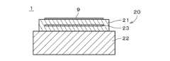
図1は、本発明の一の実施の形態に係るサセプター1の断面図である。サセプター1は、半導体製造装置において使用される半導体製造装置部材である。サセプター1は、略円板状の半導体基板9(以下、単に「基板9」と呼ぶ。)を、図1中の下側から支持する。以下の説明では、図1中の上側および下側を、単に「上側」および「下側」と呼ぶ。また、図1中の上下方向を、単に「上下方向」と呼ぶ。図1中の上下方向は、サセプター1が半導体製造装置に設置される際の実際の上下方向と必ずしも一致する必要はない。Figure 1 is a cross-sectional view of a
サセプター1は、本体部21と、ベース部22と、電極23とを備える。本体部21は、セラミックを主材料とする略板状(例えば、略円板状)の基材である。本体部21の上側の主面(すなわち、上面)上には基板9が載置される。ベース部22は、平面視において本体部21よりも大きい略板状(例えば、略円板状)の部材である。本体部21は、ベース部22上に取り付けられる。図1に示す例では、電極23は、本体部21の内部に配置(すなわち、埋設)される。電極23は、例えば、平面視において所定のパターンを描く略帯状の部材である。電極23は、比較的高い融点を有する材料により形成されることが好ましい。本体部21および電極23は、複数の材料により形成された複合焼結体である。以下の説明では、本体部21および電極23をまとめて「複合焼結体20」とも呼ぶ。本体部21および電極23の材料については後述する。なお、電極23の形状は様々に変更されてよい。また、電極23は、本体部21の表面に設けられてもよい。The
図1に示す例では、サセプター1は、電極23に直流電圧が印加されることにより発生する熱によって基板9を加熱するヒータである。すなわち、電極23は、基板9を加熱する抵抗発熱体である。サセプター1では、電極23に加えて、クーロン力またはジョンソン・ラーベック力を利用して基板9を静電吸着するチャック用電極が、本体部21の内部に設けられてもよい。あるいは、電極23がチャック用電極として利用されてもよい。In the example shown in FIG. 1, the
本体部21は、例えば、酸化アルミニウム(Al2O3)を主材料として形成されている。本体部21では、酸化マグネシウム(MgO)および/またはマグネシウムアルミニウムスピネル(MgAl2O4)等の添加材料が、Al2O3に添加されていてもよい。本体部21では、主材料であるAl2O3の含有率は、例えば95質量%以上かつ100質量%以下であり、好ましくは99質量%以上かつ100質量%以下である。本体部21におけるAl2O3の含有率は、所望する本体部21の材料特性に合わせて調整される。なお、本体部21の主材料はAl2O3には限定されず、他のセラミックであってもよい。 The
電極23は、タングステン(W)と、酸化ジルコニウム(ZrO2)とを含む。本実施の形態では、電極23は、実質的にWおよびZrO2のみにより形成されており、WおよびZrO2以外の物質を実質的に含んでいない。換言すれば、本実施の形態では、電極23におけるWおよびZrO2の合計含有率は100体積%である。 The
電極23におけるWおよびZrO2の含有率は、電極23と本体部21との熱膨張係数の差が実質的に0に近づくように調整される。また、電極23において、X線回折法(XRD)により得られるWとZrO2とのメインピークの強度比(以下、「W-ZrO2ピーク比」とも呼ぶ。)は、例えば0.90以上かつ0.96未満であり、電極23と本体部21との熱膨張係数の差が実質的に0に近づくように調整される。W-ZrO2ピーク比は、Wのメインピーク強度を、Wのメインピーク強度とZrO2のメインピーク強度との合計により除算した値である。 The content of W andZrO2 in the
Wの熱膨張係数(熱膨張率ともいう。)は、40℃以上かつ1000℃以下の範囲において、5.3ppm/℃(すなわち、ppm/K)である。以下の説明における熱膨張係数は、温度条件の記載が無い場合、40℃以上かつ1000℃以下の範囲における熱膨張係数である。ZrO2の熱膨張係数は10.5ppm/℃である。Al2O3の熱膨張係数は8.0ppm/℃である。本体部21の熱膨張係数は、主材料であるAl2O3に添加される添加材料の種類および割合により変化するが、例えば、8.1ppm/℃~8.3ppm/℃である。 The thermal expansion coefficient (also called the thermal expansion rate) of W is 5.3 ppm/°C (i.e., ppm/K) in the range of 40°C or more and 1000°C or less. In the following description, the thermal expansion coefficient is the thermal expansion coefficient in the range of 40°C or more and 1000°C or less unless temperature conditions are specified. The thermal expansion coefficient ofZrO2 is 10.5 ppm/°C. The thermal expansion coefficient ofAl2O3 is 8.0 ppm/°C. The thermal expansion coefficient of the main body21 varies depending on the type and ratio of the additive material added tothe main materialAl2O3 , but is, for example, 8.1 ppm/°C to 8.3 ppm/°C.
電極23に含まれるWの熱膨張係数は、本体部21の熱膨張係数よりも低い。電極23に含まれるZrO2の熱膨張係数は、本体部21の熱膨張係数よりも高い。40℃以上かつ1000℃以下の範囲における電極23と本体部21との熱膨張係数の差の絶対値(以下、「CTE差」とも呼ぶ。)は、例えば0.5ppm/℃以下であり、好ましくは0.2ppm/℃以下である。CTE差の下限は特に限定されないが、0.0ppm/℃以上である。 The thermal expansion coefficient of W contained in the
電極23の室温における抵抗率は、例えば3.5×10⁻⁵Ω・cm以下であり、好ましくは3.0×10⁻⁵Ω・cm以下である。当該抵抗率の下限は特に限定されないが、例えば1.0×10⁻⁵Ω・cm以上である。 The resistivity of the
電極23は、後述するように、本体部21と共に、あるいは、本体部21とは別に焼成されることにより形成される焼結体である。焼成温度は、例えば、1500℃以上の高温である。なお、Wの融点は3410℃であり、ZrO2の融点は2715℃である。Wの焼結粒径は、例えば、0.7μm以上かつ3.0μm以下であり、好ましくは、1.0μm以上かつ2.0μm以下である。ZrO2の焼結粒径は、例えば、0.7μm以上かつ3.0μm以下であり、好ましくは、1.0μm以上かつ2.0μm以下である。ZrO2の焼結粒径とWの焼結粒径との差の絶対値(以下、単に「焼結粒径差」とも呼ぶ。)は、例えば0.5μm以下であり、好ましくは0.25μm以下である。焼結粒径差の下限は特に限定されないが、例えば0.0μm以上である。WおよびZrO2の焼結粒径は、SEM(走査型電子顕微鏡)等を用いた微構造観察により求めることが可能である。 The
図2は、後述する実施例10の複合焼結体20の断面SEM画像である。図2中の上下方向の中央部の白っぽい領域は電極23に対応する。また、電極23の下側の黒い帯状の領域は、本体部21の第1部材に対応し、電極23の上側の黒い帯状の領域は、本体部21の第2部材に対応する。電極23に対応する領域内において、最も色の薄い白色の領域はWであり、Wよりも色の濃い灰色の領域はZrO2である。複合焼結体20では、上述のように電極23における焼結粒径差を小さくすることにより、電極23中におけるWおよびZrO2の分散の均一性が向上する。 2 is a cross-sectional SEM image of the compound sintered
次に、図3を参照しつつサセプター1の本体部21および電極23(すなわち、複合焼結体20)の製造方法の一例について説明する。当該例では、本体部21の下半分の略円板状の部位(以下、「第1部材」と呼ぶ。)と、上半分の略円板状の部位(以下、「第2部材」と呼ぶ。)とを作成し、第1部材と第2部材との間に電極23の材料を挟んで焼成を行うことにより、本体部21および電極23を製造する。Next, an example of a method for manufacturing the
当該製造方法では、まず、本体部21の第1部材および第2部材を準備する(ステップS11)。ステップS11において準備される第1部材および第2部材は、成形体、仮焼体および焼結体のいずれの状態であってもよい。ステップS11では、まず、本体部21(すなわち、第1部材および第2部材)の原料粉末を所定の組成となるように秤量し、当該原料粉末を湿式混合した上で、一軸加圧成形等により所定形状の成形体に成形する。In this manufacturing method, first, the first and second members of the
ステップS11では、Al2O3原料として、例えば、市販の高純度微粒粉末が使用される。また、本体部21にMgOが含まれる場合、MgO原料として、例えば、市販の高純度微粒粉末が使用される。本体部21にMgAl2O4が含まれる場合、例えば、上述の市販のMgO粉末と市販のAl2O3の高純度微粒粉末とを加熱合成したものが、MgAl2O4原料として使用される。あるいは、MgAl2O4原料として、市販のMgAl2O4の高純度微粒粉末が使用されてもよい。Al2O3原料、MgO原料およびMgAl2O4原料の純度および平均粒径等は、適宜決定される。 In step S11, for example, commercially available high-purity fine powder is used as the Al2 O3 raw material. In addition, when the
ステップS11では、原料粉末の混合条件(例えば、混合時間、溶媒種類等)は、適宜決定される。当該溶媒としては、例えば、有機溶媒またはイオン交換水が使用可能である。なお、ステップS11では、乾式混合により原料粉末が混合されてもよい。In step S11, the mixing conditions for the raw material powder (e.g., mixing time, type of solvent, etc.) are appropriately determined. As the solvent, for example, an organic solvent or ion-exchanged water can be used. In addition, in step S11, the raw material powder may be mixed by dry mixing.
ステップS11では、成形体の成形条件(例えば、付与される圧力等)は、適宜決定される。成形体の形状が板状である場合には、原料粉末がホットプレスダイス等に充填されることにより、成形体が成形されてもよい。当該成形体の成形は、形状を保持できるのであれば、他の様々な方法により行われてもよい。例えば、湿式混合後のスラリーを、流動性のある状態のままモールドに流し込んだ後に溶媒成分を除去し、所定形状の成形体としてもよい。あるいは、ドクターブレード等を利用したテープ成形法により、所定計上のテープ成形体が形成されてもよい。In step S11, the molding conditions for the green body (e.g., the applied pressure, etc.) are appropriately determined. If the green body has a plate shape, the green body may be molded by filling a hot press die or the like with the raw material powder. The green body may be molded by various other methods as long as the shape can be maintained. For example, the wet-mixed slurry may be poured into a mold while still in a fluid state, and the solvent components may be removed to form a green body of a predetermined shape. Alternatively, a tape molding method using a doctor blade or the like may be used to form a tape green body of a predetermined size.
ステップS11において、第1部材および/または第2部材の仮焼体または焼結体が準備される場合、上述の方法により形成された成形体がホットプレス法等により焼成され、仮焼体(すなわち、仮焼結体)または焼結体が形成される。当該成形体の焼成における焼成条件(例えば、プレス圧、焼成温度、焼成時間等)は、適宜決定される。また、当該成形体の焼成は、ホットプレス法以外の方法により行われてもよい。In step S11, when a calcined body or a sintered body of the first member and/or the second member is prepared, the molded body formed by the above-mentioned method is fired by a hot pressing method or the like to form a calcined body (i.e., a calcined body) or a sintered body. The firing conditions for firing the molded body (e.g., pressing pressure, firing temperature, firing time, etc.) are appropriately determined. In addition, the molded body may be fired by a method other than the hot pressing method.
次に、電極23の原料粉末を所定の組成となるように秤量し、当該原料粉末を混合した上で、溶媒およびバインダ等と混練して、電極23の前駆体である電極ペーストを生成する(ステップS12)。ステップS12では、W原料およびZrO2原料として、例えば、市販の高純度微粒粉末が使用される。W原料およびZrO2原料の純度および平均粒径等は、適宜決定される。W原料およびZrO2原料の平均粒径は、例えば、1μm未満である。 Next, the raw material powder of the
上述の電極23の原料粉末の混合は、例えば、湿式混合により行われる。原料粉末の混合条件(例えば、混合時間、溶媒種類等)は、適宜決定される。当該溶媒としては、例えば、有機溶媒またはイオン交換水が使用可能である。なお、ステップS12では、乾式混合により原料粉末が混合されてもよい。ステップS12では、原料粉末と共に混練される上記溶媒(例えば、有機溶媒)およびバインダの種類は、適宜決定される。なお、ステップS12は、ステップS11よりも前に、または、ステップS11と並行して行われてもよい。The raw material powders of the
ステップS12にて生成された電極ペーストは、ステップS11にて形成された第1部材の上面に、スクリーン印刷等により所定の形状にて付与される(ステップS13)。ステップS13において成形体である第1部材上に電極ペーストが付与される場合、第1部材は、例えばテープ成形体である。なお、ステップS13では、電極ペーストの塗布は、スクリーン印刷以外の方法により行われてもよい。第1部材が成形体または仮焼体である場合、正確には、電極ペーストは第1部材の前駆体の上面に付与される。そして、電極ペーストが大気中等において所定時間(例えば、1時間)乾燥された後、第1部材および電極ペーストの上に、第2部材が積層されて積層体が形成される(ステップS14)。The electrode paste produced in step S12 is applied in a predetermined shape by screen printing or the like to the upper surface of the first member formed in step S11 (step S13). When the electrode paste is applied to the first member, which is a molded body, in step S13, the first member is, for example, a tape molded body. Note that, in step S13, the application of the electrode paste may be performed by a method other than screen printing. When the first member is a molded body or a calcined body, more precisely, the electrode paste is applied to the upper surface of the precursor of the first member. Then, after the electrode paste is dried in the atmosphere or the like for a predetermined time (for example, 1 hour), the second member is laminated on the first member and the electrode paste to form a laminate (step S14).
なお、複合焼結体20の製造では、上述のステップS13~S14に代えて、ステップS12で生成された電極ペーストを単体で焼成して電極23を形成し、当該電極23が第1部材の上面上に配置され、第1部材および電極23上に第2部材が積層されてもよい。In addition, in the manufacture of the compound sintered
その後、ステップS14にて形成された積層体が、ホットプレス法等により焼成されることにより、第1部材と第2部材とが一体化し、本体部21および電極23(すなわち、複合焼結体20)が形成される(ステップS15)。ステップS15における焼成条件(例えば、プレス圧、焼成温度、焼成時間等)は、適宜決定される。ステップS15における焼成温度(すなわち、仮焼成時の最高温度)は、例えば、1550℃以上かつ1650℃以下である。ステップS15における積層体の焼成は、ホットプレス法以外の方法により行われてもよい。Then, the laminate formed in step S14 is sintered by a hot press method or the like, so that the first member and the second member are integrated to form the
次に、表1~表3を参照しつつ、本発明に係る複合焼結体20(すなわち、本体部21および電極23)の実施例1~13、および、複合焼結体20と比較するための比較例1~4の複合焼結体について説明する。実施例1~13では、電極23がWおよびZrO2を含むのに対し、比較例1~4では、電極23はZrO2を含まず、比較例1~2では、電極23はWも含まない。 Next, with reference to Tables 1 to 3, Examples 1 to 13 of the compound sintered body 20 (i.e., the


実施例1~13、および、比較例1~4では、本体部21および電極23の製造は、上述のステップS11~S15により行った。実施例1~13、および、比較例1~4では、ステップS11におけるAl2O3への添加剤としてMgOを使用した。Al2O3原料としては、市販のAl2O3の高純度微粒粉末(純度99.99%以上、平均粒径0.5μm)を使用した。また、MgO原料として、市販のMgOの高純度微粒粉末(純度99.9%以上、平均粒径1μm以下)を使用した。 In Examples 1 to 13 and Comparative Examples 1 to 4, the
実施例1~13、および、比較例1~4では、ステップS11における原料粉末の湿式混合は、アルミナボールおよびポリポットを用いたボールミルにより行った。混合時間は20時間であり、使用した溶媒は有機溶媒である。湿式混合により生成されたスラリーを、乾燥させた後に篩にかけることにより、本体部21の原料粉末を得た。また、ステップS11における成形体の成形は、一軸加圧成形用の金型に原料粉末を充填することにより行った。当該一軸加圧成形時の圧力は、100kgf/cm2である。得られた成形体は、直径50mm、厚さ10mmの略円板状である。なお、実施例1~13、および、比較例1~4では、実際の複合焼結体20よりも小さい試験体を作製、使用する。 In Examples 1 to 13 and Comparative Examples 1 to 4, the wet mixing of the raw material powder in step S11 was performed using a ball mill using alumina balls and a polypot. The mixing time was 20 hours, and the solvent used was an organic solvent. The slurry produced by the wet mixing was dried and then sieved to obtain the raw material powder of the
実施例1~13、および、比較例1~4では、ステップS12において、W原料およびZrO2原料として、市販のWの高純度微粒粉末(純度99.9%以上、平均粒径0.8μm)、および、ZrO2の高純度微粒粉末(純度99%以上、平均粒径0.4μm)を使用した。 In Examples 1 to 13 and Comparative Examples 1 to 4, in step S12, commercially available high-purity fine powder of W (purity 99.9% or more, average particle size 0.8 μm) and high-purity fine powder of ZrO2 (purity 99% or more, average particle size 0.4 μm) were used as the W raw material and the ZrO2 raw material.
実施例1~13、および、比較例1~4では、ステップS12における原料粉末の湿式混合は、アルミナボールおよびポリポットを用いたボールミルにより行った。混合時間は20時間であり、使用した溶媒は有機溶媒である。湿式混合により生成されたスラリーを、乾燥させた後に篩にかけることにより、電極23の原料粉末を得た。また、電極ペーストの生成時に当該原料粉末と混練される溶媒およびバインダとして、ブチルカルビトールおよびポリメタクリル酸-n-ブチルを使用した。In Examples 1 to 13 and Comparative Examples 1 to 4, the wet mixing of the raw material powder in step S12 was performed using a ball mill using alumina balls and a polypot. The mixing time was 20 hours, and the solvent used was an organic solvent. The slurry produced by the wet mixing was dried and then sieved to obtain the raw material powder of the
実施例1~13、および、比較例1~4では、ステップS13における電極ペーストの塗布は、スクリーン印刷により行われる。第1部材上に塗布された電極ペーストの形状は、幅5mm、長さ15mmの略長方形である。電極ペーストの厚さは、60μm~70μmである。In Examples 1 to 13 and Comparative Examples 1 to 4, the application of the electrode paste in step S13 is performed by screen printing. The shape of the electrode paste applied to the first member is a substantially rectangular shape with a width of 5 mm and a length of 15 mm. The thickness of the electrode paste is 60 μm to 70 μm.
実施例1~13、および、比較例1~4では、ステップS13,S14において、第1部材および第2部材として、成形体、仮焼体または焼結体のいずれかを使用した。第1部材または第2部材として成形体を使用する場合、上述のステップS11で得られたものを使用する。In Examples 1 to 13 and Comparative Examples 1 to 4, in steps S13 and S14, either a compact, a calcined body, or a sintered body was used as the first member and the second member. When a compact is used as the first member or the second member, the one obtained in step S11 described above is used.
第1部材または第2部材として仮焼体を使用する場合、前述した成形体と同様の手法で成形体を作製し、熱処理をして作製した。焼成温度(すなわち、熱処理時の最高温度)は、800℃以上かつ1000℃以下である。そして、得られた仮焼体を、直径50mm、厚さ5mmの略円板状に加工した。なお、仮焼体は、原料粉末に有機バインダなどの成形助剤を添加して保形した成形体を加熱処理して作製するなど、既存の方法を適宜採用すればよく、その作製条件は上記に限定されるものではない。When a calcined body is used as the first or second member, a molded body is prepared in the same manner as the molded body described above, and then heat-treated to produce it. The firing temperature (i.e., the maximum temperature during heat treatment) is 800°C or higher and 1000°C or lower. The obtained calcined body is then processed into a roughly disk-like shape with a diameter of 50 mm and a thickness of 5 mm. Note that the calcined body can be produced by appropriately adopting existing methods, such as by adding a molding aid such as an organic binder to the raw material powder and heat-treating a molded body that has been shaped to retain its shape, and the production conditions are not limited to those described above.
第1部材または第2部材として焼結体を使用する場合、ホットプレス法により成形体の焼成を行った。具体的には、上述の成形体をホットプレス用の黒鉛型に収容し、ホットプレス炉にセットして焼成を行った。仮焼成時のプレス圧は、200kgf/cm2である。焼成温度(すなわち、仮焼成時の最高温度)は、1550℃以上かつ1650℃以下である。焼成時間は、8時間である。昇温速度および降温速度は、300℃/hである。焼成雰囲気は、1000℃までの昇温時は真空引きを行い、その後は窒素ガスを導入した。窒素ガスの導入後のガス圧力は、約1.5atm(約0.152MPa)に維持した。降温時は、1400℃で温度制御を停止し、炉冷した。そして、得られた焼結体を、直径50mm、厚さ5mmの略円板状に加工した。 When a sintered body was used as the first member or the second member, the molded body was sintered by hot pressing. Specifically, the above-mentioned molded body was placed in a graphite mold for hot pressing and set in a hot press furnace to perform sintering. The press pressure during pre-sintering was 200 kgf/cm2 . The sintering temperature (i.e., the maximum temperature during pre-sintering) was 1550°C or higher and 1650°C or lower. The sintering time was 8 hours. The temperature increase rate and temperature decrease rate were 300°C/h. The sintering atmosphere was evacuated when the temperature was increased to 1000°C, and nitrogen gas was introduced thereafter. The gas pressure after the introduction of nitrogen gas was maintained at about 1.5 atm (about 0.152 MPa). When the temperature was decreased, the temperature control was stopped at 1400°C and the furnace was cooled. The obtained sintered body was then processed into a roughly circular plate shape with a diameter of 50 mm and a thickness of 5 mm.
実施例1~13、および、比較例1~4では、ステップS15における積層後の焼成は、ホットプレス法により行った。具体的には、上述の積層体をホットプレス用の黒鉛型に収容し、ホットプレス炉にセットして焼成を行った。焼成時のプレス圧は、200kgf/cm2である。焼成温度(すなわち、焼成時の最高温度)は、1550℃以上かつ1650℃以下である。焼成時間は、4時間~8時間である。昇温速度および降温速度は、300℃/hである。焼成雰囲気は、窒素ガス雰囲気である。 In Examples 1 to 13 and Comparative Examples 1 to 4, the sintering after lamination in step S15 was performed by hot pressing. Specifically, the above-mentioned laminate was placed in a graphite mold for hot pressing, and sintered by setting it in a hot press furnace. The pressing pressure during sintering was 200 kgf/cm2 . The sintering temperature (i.e., the maximum temperature during sintering) was 1550°C or higher and 1650°C or lower. The sintering time was 4 hours to 8 hours. The temperature increase rate and temperature decrease rate were 300°C/h. The sintering atmosphere was a nitrogen gas atmosphere.
表1~表3において、基材(すなわち、本体部21の第1部材および第2部材)の熱膨張係数は、本体部21から切り出した焼結体試料を用いて、JIS-R1618に準じた方法により、40℃~1000℃の範囲で測定した。また、実施例1~13の電極23の熱膨張係数は、WおよびZrO2のそれぞれ単体の熱膨張係数と、電極23におけるWおよびZrO2の含有率とに基づいて求めた。具体的には、W単体の熱膨張係数と電極23におけるWの含有率(体積%)との積、および、ZrO2単体の熱膨張係数と電極23におけるZrO2の含有率(体積%)との積の合計を、電極23の熱膨張係数とした。WおよびZrO2のそれぞれ単体の熱膨張係数は、ステップS12で使用した市販のW粉末およびZrO2粉末をステップS11と同様の条件でホットプレス焼成して作製されたバルク材を用いて、JIS-R1618に準じた方法により、40℃~1000℃の範囲で測定した。比較例1~4においても同様である。CTE差は、上述のように、電極23の熱膨張係数と本体部21の熱膨張係数の差の絶対値である。 In Tables 1 to 3, the thermal expansion coefficient of the base material (i.e., the first and second members of the main body 21) was measured in the range of 40°C to 1000°C by a method conforming to JIS-R1618 using a sintered body sample cut out from the
電極23におけるW-ZrO2ピーク比は、上述のXRDにより測定されたWとZrO2とのメインピークの強度比である。W-ZrO2ピーク比は、Wのメインピークである(110)面の強度をI1とし、ZrO2のメインピークである(111)面の強度をI2として、I1/(I1+I2)を算出した。また、XRDによる測定の際には、第2部材を除去し、第1部材上に位置する電極23を露出させて測定を行った。X線回折装置として、封入管式X線回折装置(ブルカー・エイエックスエス株式会社製 D8-ADVANCE)を使用した。測定条件はCuKα、40kV、40mA、2θ=10~70°、ステップ幅を0.002°とした。 The W-ZrO2 peak ratio in the
電極23におけるWの焼結粒径は、SEMを用いた微構造観察により求めた。具体的には、試験片の一面を鏡面状に研磨仕上げし、電極23の研磨面をSEMを用いて観察する。そして、所定数(例えば、数十個)の焼結粒子のそれぞれの長径および短径の平均である平均径を算出し、当該所定数の焼結粒子の平均径の算術平均をWの焼結粒径とした。電極23におけるZrO2の焼結粒径についても同様である。 The grain size of the sintered W in the
電極23の抵抗率は、次のように求めた。まず、ステップS15にて形成された複合焼結体20から、幅、長さおよび厚さがそれぞれ9mmの略直方体状の試験片を切り出す。試験片は、中央部に幅5mm、長さ9mmの電極23が内蔵されるように切り出される。試験片の両端面には、幅5mmの電極23が露出している。電極23の断面積S(cm2)は、試験片の端面における電極23の幅および長さを光学顕微鏡により測定して求めた。また、電極23が露出する試験片の両端面間の距離をノギスにより測定し、電極23の長さL(cm)とした。抵抗測定用の回路は、電極23の両端面に導電性ペーストを塗布した上でリード線を接続して構成した。そして、大気中、室温において、電極23に微少電流I(mA)を0mA~150mAの範囲で付与し、その際に発生する微小電圧値V(mV)を測定し、電極23の抵抗R(Ω)をR=V/Iにより求めた。その後、電極23の抵抗率ρ(Ω・cm)を、ρ=R×S/Lにより求めた。 The resistivity of the
電極23の組成は、次のように求めた。まず、試験片の上半分または下半分を除去して電極23の上面または下面を露出させ、露出した電極23を研磨した。そして、電極23の研磨面において、上述のX線回折装置により上記測定条件にて結晶相を同定した。The composition of
実施例1~13、および、比較例1~4では、本体部21の主材料はAl2O3であり、添加物はMgOである。また、上述のように、実施例1~13では、電極23はWおよびZrO2により形成される。換言すれば、実施例1~13では、電極23におけるWおよびZrO2の合計含有率は、100体積%である。一方、比較例1では、電極23は炭化タングステン(WC)のみにより形成され、WおよびZrO2を含まない。比較例2では、電極23は、WCおよびAl2O3により形成され、WおよびZrO2を含まない。比較例3では、電極23は、Wのみにより形成され、ZrO2を含まない。比較例4では、電極23は、WおよびAl2O3により形成され、ZrO2を含まない。 In Examples 1 to 13 and Comparative Examples 1 to 4, the main material of the
実施例1では、ステップS13において電極ペーストが付与される本体部21の第1部材は焼結体である。また、ステップS14において第1部材上に積層される第2部材は成形体である。本体部21のMgOの含有率は0.025質量%であり、本体部21の熱膨張係数は8.1ppm/℃である。なお、本体部21のMgO以外の残部はAl2O3である(他の実施例および比較例においても同様)。電極23におけるWの含有率は46.2体積%であり、ZrO2の含有率は53.8体積%である。電極23の熱膨張係数は8.1ppm/℃である。複合焼結体20の焼成温度(すなわち、焼成時の最高温度)は1600℃である。 In Example 1, the first member of the
実施例1では、CTE差(すなわち、40℃以上かつ1000℃以下の範囲における電極23と本体部21との熱膨張係数の差の絶対値)は0.0ppm/℃であった。W-ZrO2ピーク比は0.94であった。WおよびZrO2の焼結粒径はそれぞれ、1.17μmおよび1.27μmであり、焼結粒径差(すなわち、ZrO2の焼結粒径とWの焼結粒径との差の絶対値)は0.10μmであった。電極23の抵抗率は、2.9×10-5Ω・cmであった。電極23の組成は、WおよびZrO2であった。 In Example 1, the CTE difference (i.e., the absolute value of the difference in the thermal expansion coefficient between the
実施例1では、CTE差が0.5ppm/℃以下と小さいため、本体部21と電極23との熱膨張係数の差に起因する本体部21のクラックや電極23の剥離は生じなかった。また、電極23の抵抗率は3.5×10-5Ω・cm以下と小さかった。W-ZrO2ピーク比は、0.90以上かつ0.96未満と好適な範囲であり、これにより、上述の熱膨張係数の差の低減および抵抗率の増大抑制を好適に両立することができる。ZrO2の焼結粒径は、0.7μm以上かつ3.0μm以下と好適な範囲であり、焼結粒径差(すなわち、Wの焼結粒径とZrO2の焼結粒径との差)は0.5μm以下と小さかった。このため、電極23中において、WおよびZrO2の略均等な分散が実現された。 In Example 1, since the CTE difference was small, 0.5 ppm/°C or less, no cracks in the
実施例2では、本体部21におけるMgOの含有率が1.0質量%であり、本体部21の熱膨張係数は8.2ppm/℃である。電極23におけるWの含有率は44.2体積%であり、ZrO2の含有率は55.8体積%である。電極23の熱膨張係数は8.2ppm/℃である。その他の条件は、実施例1と同様である。 In Example 2, the MgO content in the
実施例2では、CTE差は0.0ppm/℃であった。W-ZrO2ピーク比は0.93であった。WおよびZrO2の焼結粒径はそれぞれ、1.15μmおよび1.32μmであり、焼結粒径差は0.17μmであった。電極23の抵抗率は、3.0×10-5Ω・cmであった。電極23の組成は、WおよびZrO2であった。 In Example 2, the CTE difference was 0.0 ppm/°C. The W-ZrO2 peak ratio was 0.93. Thesintered grain sizes of W andZrO2 were 1.15 μm and 1.32 μm, respectively, and the sintered grain size difference was 0.17 μm. The resistivity of the
実施例2では、CTE差が小さいため、本体部21と電極23との熱膨張係数の差に起因する本体部21のクラックや電極23の剥離は生じなかった。また、電極23の抵抗率は小さかった。さらに、ZrO2の焼結粒径が好適な範囲であり、焼結粒径差が小さいため、電極23中において、WおよびZrO2の略均等な分散が実現された。 In Example 2, since the CTE difference was small, no cracks occurred in the
実施例3では、本体部21におけるMgOの含有率が5.0質量%であり、本体部21の熱膨張係数は8.3ppm/℃である。電極23におけるWの含有率は42.3体積%であり、ZrO2の含有率は57.7体積%である。電極23の熱膨張係数は8.3ppm/℃である。その他の条件は、実施例1と同様である。 In Example 3, the content of MgO in the
実施例3では、CTE差は0.0ppm/℃であった。W-ZrO2ピーク比は0.91であった。WおよびZrO2の焼結粒径はそれぞれ、1.14μmおよび1.36μmであり、焼結粒径差は0.22μmであった。電極23の抵抗率は、3.2×10-5Ω・cmであった。電極23の組成は、WおよびZrO2であった。 In Example 3, the CTE difference was 0.0 ppm/°C. The W-ZrO2 peak ratio was 0.91. Thesintered grain sizes of W andZrO2 were 1.14 μm and 1.36 μm, respectively, and the sintered grain size difference was 0.22 μm. The resistivity of the
実施例3では、CTE差が小さいため、本体部21と電極23との熱膨張係数の差に起因する本体部21のクラックや電極23の剥離は生じなかった。また、電極23の抵抗率は小さかった。さらに、ZrO2の焼結粒径が好適な範囲であり、焼結粒径差が小さいため、電極23中において、WおよびZrO2の略均等な分散が実現された。 In Example 3, since the CTE difference was small, no cracks occurred in the
実施例1~3に注目すると、本体部21の熱膨張係数を上記範囲(すなわち、8.1ppm/℃~8.3ppm/℃)で変更した場合であっても、CTE差を0.0ppm/℃とすることができ、本体部21のクラックや電極23の剥離を防止することができた。また、電極23の抵抗率の増大を抑制することができた。Focusing on Examples 1 to 3, even when the thermal expansion coefficient of the
実施例4では、電極23におけるWの含有率は55.8体積%であり、ZrO2の含有率は44.2体積%である。電極23の熱膨張係数は7.6ppm/℃である。その他の条件は、実施例1と同様である。 In Example 4, the W content of the
実施例4では、CTE差は0.5ppm/℃であった。W-ZrO2ピーク比は0.96であった。WおよびZrO2の焼結粒径はそれぞれ、1.20μmおよび1.11μmであり、焼結粒径差は0.09μmであった。電極23の抵抗率は、2.0×10-5Ω・cmであった。電極23の組成は、WおよびZrO2であった。 In Example 4, the CTE difference was 0.5 ppm/°C. The W-ZrO2 peak ratio was 0.96. The sintered grain sizes of W andZrO2 were 1.20 μm and 1.11 μm, respectively, and the sintered grain size difference was 0.09 μm. The resistivity of the
実施例4では、CTE差が小さいため(すなわち、0.5ppm/℃以下であるため)、本体部21と電極23との熱膨張係数の差に起因する本体部21のクラックや電極23の剥離は生じなかった。また、電極23の抵抗率は小さかった。さらに、ZrO2の焼結粒径が好適な範囲であり、焼結粒径差が小さいため、電極23中において、WおよびZrO2の略均等な分散が実現された。 In Example 4, since the CTE difference was small (i.e., 0.5 ppm/°C or less), no cracks in the
実施例5では、電極23におけるWの含有率は51.9体積%であり、ZrO2の含有率は48.1体積%である。電極23の熱膨張係数は7.8ppm/℃である。その他の条件は、実施例1と同様である。 In Example 5, the W content in the
実施例5では、CTE差は0.3ppm/℃であった。W-ZrO2ピーク比は0.95であった。WおよびZrO2の焼結粒径はそれぞれ、1.19μmおよび1.14μmであり、焼結粒径差は0.05μmであった。電極23の抵抗率は、2.5×10-5Ω・cmであった。電極23の組成は、WおよびZrO2であった。 In Example 5, the CTE difference was 0.3 ppm/°C. The W-ZrO2 peak ratio was 0.95. Thesintered grain sizes of W andZrO2 were 1.19 μm and 1.14 μm, respectively, and the sintered grain size difference was 0.05 μm. The resistivity of the
実施例5では、CTE差が小さいため、本体部21と電極23との熱膨張係数の差に起因する本体部21のクラックや電極23の剥離は生じなかった。また、電極23の抵抗率は小さかった。さらに、ZrO2の焼結粒径が好適な範囲であり、焼結粒径差が小さいため、電極23中において、WおよびZrO2の略均等な分散が実現された。 In Example 5, since the CTE difference was small, no cracks occurred in the
実施例6では、電極23におけるWの含有率は48.1体積%であり、ZrO2の含有率は51.9体積%である。電極23の熱膨張係数は8.0ppm/℃である。その他の条件は、実施例1と同様である。 In Example 6, the W content of the
実施例6では、CTE差は0.1ppm/℃であった。W-ZrO2ピーク比は0.95であった。WおよびZrO2の焼結粒径はそれぞれ、1.18μmおよび1.22μmであり、焼結粒径差は0.04μmであった。電極23の抵抗率は、2.8×10-5Ω・cmであった。電極23の組成は、WおよびZrO2であった。 In Example 6, the CTE difference was 0.1 ppm/°C. The W-ZrO2 peak ratio was 0.95. The sintered grain sizes of W andZrO2 were 1.18 μm and 1.22 μm, respectively, and the sintered grain size difference was 0.04 μm. The resistivity of the
実施例6では、CTE差が小さいため、本体部21と電極23との熱膨張係数の差に起因する本体部21のクラックや電極23の剥離は生じなかった。また、電極23の抵抗率は小さかった。さらに、ZrO2の焼結粒径が好適な範囲であり、焼結粒径差が小さいため、電極23中において、WおよびZrO2の略均等な分散が実現された。 In Example 6, since the CTE difference was small, no cracks occurred in the
実施例7では、電極23におけるWの含有率は44.2体積%であり、ZrO2の含有率は55.8体積%である。電極23の熱膨張係数は8.2ppm/℃である。その他の条件は、実施例1と同様である。 In Example 7, the W content of the
実施例7では、CTE差は0.1ppm/℃であった。W-ZrO2ピーク比は0.93であった。WおよびZrO2の焼結粒径はそれぞれ、1.16μmおよび1.30μmであり、焼結粒径差は0.14μmであった。電極23の抵抗率は、3.1×10-5Ω・cmであった。電極23の組成は、WおよびZrO2であった。 In Example 7, the CTE difference was 0.1 ppm/°C. The W-ZrO2 peak ratio was 0.93. The sintered grain sizes of W andZrO2 were 1.16 μm and 1.30 μm, respectively, and the sintered grain size difference was 0.14 μm. The resistivity of the
実施例7では、CTE差が小さいため、本体部21と電極23との熱膨張係数の差に起因する本体部21のクラックや電極23の剥離は生じなかった。また、電極23の抵抗率は小さかった。さらに、ZrO2の焼結粒径が好適な範囲であり、焼結粒径差が小さいため、電極23中において、WおよびZrO2の略均等な分散が実現された。 In Example 7, since the CTE difference was small, no cracks occurred in the
実施例8では、電極23におけるWの含有率は40.4体積%であり、ZrO2の含有率は59.6体積%である。電極23の熱膨張係数は8.4ppm/℃である。その他の条件は、実施例1と同様である。 In Example 8, the W content of the
実施例8では、CTE差は0.3ppm/℃であった。W-ZrO2ピーク比は0.91であった。WおよびZrO2の焼結粒径はそれぞれ、1.14μmおよび1.35μmであり、焼結粒径差は0.21μmであった。電極23の抵抗率は、3.3×10-5Ω・cmであった。電極23の組成は、WおよびZrO2であった。 In Example 8, the CTE difference was 0.3 ppm/°C. The W-ZrO2 peak ratio was 0.91. The sintered grain sizes of W andZrO2 were 1.14 μm and 1.35 μm, respectively, and the sintered grain size difference was 0.21 μm. The resistivity of the
実施例8では、CTE差が小さいため、本体部21と電極23との熱膨張係数の差に起因する本体部21のクラックや電極23の剥離は生じなかった。また、電極23の抵抗率は小さかった。さらに、ZrO2の焼結粒径が好適な範囲であり、焼結粒径差が小さいため、電極23中において、WおよびZrO2の略均等な分散が実現された。 In Example 8, since the CTE difference was small, no cracks occurred in the
実施例9では、電極23におけるWの含有率は36.5体積%であり、ZrO2の含有率は63.5体積%である。電極23の熱膨張係数は8.6ppm/℃である。その他の条件は、実施例1と同様である。 In Example 9, the W content of the
実施例9では、CTE差は0.5ppm/℃であった。W-ZrO2ピーク比は0.90であった。WおよびZrO2の焼結粒径はそれぞれ、1.13μmおよび1.38μmであり、焼結粒径差は0.25μmであった。電極23の抵抗率は、3.5×10-5Ω・cmであった。電極23の組成は、WおよびZrO2であった。 In Example 9, the CTE difference was 0.5 ppm/°C. The W-ZrO2 peak ratio was 0.90. The sintered grain sizes of W andZrO2 were 1.13 μm and 1.38 μm, respectively, and the sintered grain size difference was 0.25 μm. The resistivity of the
実施例9では、CTE差が小さいため、本体部21と電極23との熱膨張係数の差に起因する本体部21のクラックや電極23の剥離は生じなかった。また、電極23の抵抗率は小さかった。さらに、ZrO2の焼結粒径が好適な範囲であり、焼結粒径差が小さいため、電極23中において、WおよびZrO2の略均等な分散が実現された。 In Example 9, since the CTE difference was small, no cracks occurred in the
実施例1,4~9に注目すると、電極23におけるWおよびZrO2の含有率を変更し、CTE差を上記範囲(すなわち、0.0ppm/℃~0.5ppm/℃)で変更した場合であっても、本体部21のクラックや電極23の剥離を防止することができた。また、電極23の抵抗率の増大を抑制することができた。 Focusing on Examples 1, 4 to 9, even when the content of W andZrO2 in the
実施例10では、複合焼結体20の焼成温度は1550℃である。その他の条件は、実施例1と同様である。In Example 10, the sintering temperature of the compound sintered
実施例10では、電極23の熱膨張係数は8.0ppm/℃であり、CTE差は0.1ppm/℃であった。W-ZrO2ピーク比は0.94であった。WおよびZrO2の焼結粒径はそれぞれ、0.94μmおよび0.82μmであり、焼結粒径差は0.12μmであった。電極23の抵抗率は、3.0×10-5Ω・cmであった。電極23の組成は、WおよびZrO2であった。 In Example 10, the thermal expansion coefficient of the
実施例10では、CTE差が小さいため、本体部21と電極23との熱膨張係数の差に起因する本体部21のクラックや電極23の剥離は生じなかった。また、電極23の抵抗率は小さかった。さらに、ZrO2の焼結粒径が好適な範囲であり、焼結粒径差が小さいため、電極23中において、WおよびZrO2の略均等な分散が実現された。 In Example 10, since the CTE difference was small, no cracks occurred in the
実施例11では、複合焼結体20の焼成温度は1650℃である。その他の条件は、実施例1と同様である。In Example 11, the sintering temperature of the compound sintered
実施例11では、電極23の熱膨張係数は8.2ppm/℃であり、CTE差は0.1ppm/℃であった。W-ZrO2ピーク比は0.93であった。WおよびZrO2の焼結粒径はそれぞれ、1.81μmおよび1.72μmであり、焼結粒径差は0.09μmであった。電極23の抵抗率は、3.1×10-5Ω・cmであった。電極23の組成は、WおよびZrO2であった。 In Example 11, the thermal expansion coefficient of the
実施例11では、CTE差が小さいため、本体部21と電極23との熱膨張係数の差に起因する本体部21のクラックや電極23の剥離は生じなかった。また、電極23の抵抗率は小さかった。さらに、ZrO2の焼結粒径が好適な範囲であり、焼結粒径差が小さいため、電極23中において、WおよびZrO2の略均等な分散が実現された。 In Example 11, since the CTE difference was small, no cracks occurred in the
実施例1,10~11に注目すると、複合焼結体20の焼成温度を上記範囲(すなわち、1550℃~1650℃)で変更した場合であっても、CTE差は0.0ppm/℃~0.1ppm/℃と小さく、本体部21のクラックや電極23の剥離を防止することができた。また、電極23の抵抗率の増大を抑制することができた。Focusing on Examples 1, 10 to 11, even when the firing temperature of the compound sintered
実施例12では、ステップS11において準備される第1部材、および、ステップS14において第1部材上に積層される第2部材は仮焼体である。その他の条件は、実施例1と同様である。In Example 12, the first member prepared in step S11 and the second member stacked on the first member in step S14 are calcined bodies. The other conditions are the same as in Example 1.
実施例12では、CTE差は0.0ppm/℃であった。W-ZrO2ピーク比は0.93であった。WおよびZrO2の焼結粒径はそれぞれ、2.22μmおよび2.55μmであり、焼結粒径差は0.33μmであった。電極23の抵抗率は、2.8×10-5Ω・cmであった。電極23の組成は、WおよびZrO2であった。 In Example 12, the CTE difference was 0.0 ppm/°C. The W-ZrO2 peak ratio was 0.93. The sintered grain sizes of W andZrO2 were 2.22 μm and 2.55 μm, respectively, and the sintered grain size difference was 0.33 μm. The resistivity of the
実施例12では、CTE差が小さいため、本体部21と電極23との熱膨張係数の差に起因する本体部21のクラックや電極23の剥離は生じなかった。また、電極23の抵抗率は小さかった。さらに、ZrO2の焼結粒径が好適な範囲であり、焼結粒径差が小さいため、電極23中において、WおよびZrO2の略均等な分散が実現された。 In Example 12, since the CTE difference was small, no cracks occurred in the
実施例13では、ステップS14において第1部材上に積層される第2部材は焼結体である。その他の条件は、実施例1と同様である。In Example 13, the second member that is layered on the first member in step S14 is a sintered body. The other conditions are the same as in Example 1.
実施例13では、CTE差は0.0ppm/℃であった。W-ZrO2ピーク比は0.94であった。WおよびZrO2の焼結粒径はそれぞれ、1.15μmおよび1.25μmであり、焼結粒径差は0.10μmであった。電極23の抵抗率は、2.9×10-5Ω・cmであった。電極23の組成は、WおよびZrO2であった。 In Example 13, the CTE difference was 0.0 ppm/°C. The W-ZrO2 peak ratio was 0.94. The sintered grain sizes of W andZrO2 were 1.15 μm and 1.25 μm, respectively, and the sintered grain size difference was 0.10 μm. The resistivity of the
実施例13では、CTE差が小さいため、本体部21と電極23との熱膨張係数の差に起因する本体部21のクラックや電極23の剥離は生じなかった。また、電極23の抵抗率は小さかった。さらに、ZrO2の焼結粒径が好適な範囲であり、焼結粒径差が小さいため、電極23中において、WおよびZrO2の略均等な分散が実現された。 In Example 13, since the CTE difference was small, no cracks occurred in the
実施例1,12~13に注目すると、ステップS15における焼結前の第1部材および第2部材の状態(すなわち、成形体、仮焼体または焼結体)を変更した場合であっても、CTE差は0.0ppm/℃であり、本体部21のクラックや電極23の剥離を防止することができた。また、電極23の抵抗率の増大を抑制することができた。Focusing on Examples 1, 12 and 13, even when the state of the first and second members before sintering in step S15 (i.e., compact, calcined body or sintered body) was changed, the CTE difference was 0.0 ppm/°C, and cracks in the
比較例1では、上述のように、電極23がWCのみにより形成され、WおよびZrO2を含まない。電極23の熱膨張係数は5.3ppm/℃である。その他の条件は、実施例1と同様である。比較例1では、CTE差が2.8ppm/℃と大きいため、本体部21と電極23との熱膨張係数の差に起因する本体部21のクラックや電極23の剥離が生じた。また、電極23の組成は、WCおよびW2Cであった。当該W2Cは、高温焼成によりWCの一部が酸化し生成されたものであり、電極23におけるWCおよびW2Cの含有率が変動して電極23の特性(例えば、抵抗率、熱膨張係数等)が不安定化する可能性がある。 In Comparative Example 1, as described above, the
比較例2では、上述のように、電極23がWCおよびAl2O3により形成され、WおよびZrO2を含まない。電極23の熱膨張係数は6.1ppm/℃である。その他の条件は、実施例1と同様である。比較例2では、CTE差が2.0ppm/℃と大きいため、本体部21と電極23との熱膨張係数の差に起因する本体部21のクラックや電極23の剥離が生じた。また、電極23の組成は、WC、W2CおよびAl2O3であった。したがって、比較例1と同様に、電極23の特性が不安定化する可能性がある。 In Comparative Example 2, as described above, the
比較例3では、上述のように、電極23がWのみにより形成され、ZrO2を含まない。電極23の熱膨張係数は5.3ppm/℃である。その他の条件は、実施例1と同様である。比較例3では、CTE差が2.5ppm/℃と大きいため、本体部21と電極23との熱膨張係数の差に起因する本体部21のクラックや電極23の剥離が生じた。また、電極23の組成は、Wであった。 In Comparative Example 3, as described above, the
比較例4では、上述のように、電極23がWおよびAl2O3により形成され、ZrO2を含まない。電極23の熱膨張係数は6.1ppm/℃である。その他の条件は、実施例1と同様である。比較例4では、CTE差が2.0ppm/℃と大きいため、本体部21と電極23との熱膨張係数の差に起因する本体部21のクラックや電極23の剥離が生じた。また、電極23の組成は、WおよびAl2O3であった。 In Comparative Example 4, as described above, the
以上に説明したように、複合焼結体20は、セラミックを主材料とする基材(上記例では、本体部21)と、当該基材の内部または表面に配置される電極23と、を備える。電極23は、Wと、ZrO2とを含む。これにより、実施例1~13に示すように、電極23と基材との熱膨張係数の差を小さくすることができる。その結果、電極23と基材との熱膨張係数の差に起因する基材のクラックや電極23の剥離を抑制することができる。また、複合焼結体20では、電極23の抵抗率の増大を抑制することもできる。その結果、電極23による発熱量を精度良く制御することができる。さらに、WおよびZrO2は、NiやCoのような磁性材料ではないため、複合焼結体20を静電チャックとして使用する場合であっても、クーロン力による基板9の吸着の阻害を抑制することができる。 As described above, the compound sintered
上述のように、電極23と基材との熱膨張係数の差の絶対値は、40℃以上かつ1000℃以下の範囲において、0.5ppm/℃以下であることが好ましい。これにより、電極23と基材との熱膨張係数の差に起因する基材のクラックや電極23の剥離をさらに抑制することができる。As described above, the absolute value of the difference in thermal expansion coefficient between the
上述のように、電極23の室温における抵抗率は、3.5×10⁻⁵Ω・cm以下であることが好ましい。これにより、電極23による発熱量をさらに精度良く制御することができる。 As described above, the resistivity of the
上述のように、電極23において、X線回折法により得られるWとZrO2とのメインピークの強度比(すなわち、W-ZrO2ピーク比)は、0.90以上かつ0.96未満であることが好ましい。このように、電極23におけるWとZrO2との組成比を好適な範囲とすることにより、電極23の抵抗率の増大を好適に抑制しつつ、電極23と基材との熱膨張係数の差を好適に小さくすることができる。 As described above, in the
上述のように、電極23におけるWおよびZrO2の合計含有率は、100体積%であることが好ましい。これにより、電極23の材料の種類増加による製造コスト増大を防止することができる。 As described above, the total content of W andZrO2 in the
上述のように、ZrO2の焼結粒径は、0.7μm以上かつ3.0μm以下であることが好ましい。これにより、電極23中におけるZrO2の分散の均一性を向上することができる。その結果、電極23全体において、抵抗率の増大抑制、および、基材との熱膨張係数差の低減を実現することができる。 As described above, the grain size of the sinteredZrO2 is preferably 0.7 μm or more and 3.0 μm or less. This can improve the uniformity of the dispersion ofZrO2 in the
上述のように、ZrO2の焼結粒径とWの焼結粒径との差の絶対値(すなわち、焼結粒径差)は、0.5μm以下であることが好ましい。これにより、電極23中におけるWおよびZrO2の分散の均一性を向上することができる。その結果、電極23全体において、抵抗率の増大抑制、および、基材との熱膨張係数差の低減を実現することができる。 As described above, the absolute value of the difference between the sintered grain size ofZrO2 and the sintered grain size of W (i.e., the sintered grain size difference) is preferably 0.5 μm or less. This can improve the uniformity of the dispersion of W andZrO2 in the
上述のように、基材の主材料はAl2O3であり、当該基材におけるAl2O3の含有率は95質量%以上であることが好ましい。これにより、複合焼結体20を製造する際に、複合焼結体20の高温焼成が可能となる。このため、焼成時におけるWの炭化および酸化を抑制することができる。その結果、電極23の特性を安定させることができる。 As described above, the main material of the base material is Al2 O3 , and the content of Al2 O3 in the base material is preferably 95 mass % or more. This allows the compound sintered
上述のように、複合焼結体20では、電極23の抵抗率の増大を抑制しつつ、電極23と基材との熱膨張係数の差を小さくして、基材のクラックや電極23の剥離を抑制することができる。このため、複合焼結体20は、半導体製造装置において使用される半導体製造装置部材に適している。複合焼結体20は、特に、ハイパワーエッチング装置等の高出力半導体製造装置において使用される半導体製造装置部材に適している。複合焼結体20を用いて作成される半導体製造装置部材の好適な一例として、上述のサセプター1が挙げられる。サセプター1では、上述のように、本体部21は円板状であり、本体部21の主面に基板9が載置される。 As described above, in the compound sintered
上述の複合焼結体20の製造方法は、セラミックを主材料とする成形体、仮焼体または焼結体である第1部材および第2部材を準備する工程(ステップS11)と、当該第1部材上に、WおよびZrO2を含む電極23または電極23の前駆体を配置した後、第2部材を積層して積層体を形成する工程(ステップS13,S14)と、当該積層体をホットプレス焼成する工程(ステップS15)と、を備える。これにより、上記と同様に、電極23と基材との熱膨張係数の差に起因する基材のクラックや電極23の剥離を抑制することができる。 The manufacturing method of the above-mentioned compound sintered
上述のように、ステップS15の終了後における電極23と第1部材および第2部材との熱膨張係数の差の絶対値は、40℃以上かつ1000℃以下の範囲において、0.5ppm/℃以下であることが好ましい。これにより、これにより、電極23と基材との熱膨張係数の差に起因する基材のクラックや電極23の剥離をさらに抑制することができる。As described above, it is preferable that the absolute value of the difference in the thermal expansion coefficient between the
上述のように、ステップS15における焼成温度は、1550℃以上かつ1650℃以下であることが好ましい。これにより、焼成時におけるWの炭化および酸化を抑制することができる。その結果、電極23の特性を安定させることができる。As described above, the firing temperature in step S15 is preferably 1550°C or higher and 1650°C or lower. This makes it possible to suppress carbonization and oxidation of W during firing. As a result, the characteristics of the
上述の複合焼結体20、半導体製造装置部材、および、複合焼結体20の製造方法では、様々な変更が可能である。Various modifications are possible in the above-described compound sintered
例えば、複合焼結体20のCTE差は、0.5ppm/℃よりも大きくてもよい。For example, the CTE difference of the compound sintered
電極23の室温における抵抗率は、3.5×10⁻⁵Ω・cmよりも高くてもよい。 The resistivity of the
本発明に関連する技術に係る電極23では、W-ZrO2ピーク比は0.90未満であってもよく、0.96以上であってもよい。
In the
電極23中の固形物におけるWおよびZrO2の合計含有率は、100体積%未満であってもよい。 The total content of W andZrO2 in the solids in
電極23におけるZrO2の焼結粒径は、0.7μm未満であってもよく、3.0μmよりも大きくてもよい。 The sintered grain size ofZrO2 in the
電極23において、ZrO2の焼結粒径とWの焼結粒径との差の絶対値(すなわち、焼結粒径差)は、0.5μmよりも大きくてもよい。 In the
本体部21におけるAl2O3の含有率は、95質量%未満であってもよい。また、本体部21の主材料は、Al2O3以外のセラミックであってもよい。 The content of Al2 O3 in the
複合焼結体20の製造方法では、上述のステップS15における焼成温度は、1550℃未満であってもよく、1650℃よりも高温であってもよい。In the manufacturing method of the compound sintered
複合焼結体20は、上記製造方法とは異なる方法により製造されてもよい。例えば、ステップS12が省略され、ステップS13において、電極23の原料粉末(すなわち、電極23の前駆体)が第1部材上に付与されてもよい。The compound sintered
複合焼結体20は、サセプター1以外にも、半導体製造装置に設けられる他の半導体製造装置部材(例えば、リング、シャワーヘッド等)の作製に用いられてよい。また、複合焼結体20により半導体製造装置以外の装置にて使用される部材が作製されてもよい。例えば、複合焼結体20は、半導体基板以外の基板を支持するサセプターの作製に用いられてもよく、対象物を加熱するセラミックヒーターの作製に用いられてもよい。In addition to the
上記実施の形態および各変形例における構成は、相互に矛盾しない限り適宜組み合わされてよい。The configurations in the above embodiment and each modified example may be combined as appropriate as long as they are not mutually inconsistent.
本発明は、半導体製造装置に関する分野、例えば、半導体基板を保持して加熱するサセプターの製造に利用可能である。The present invention can be used in the field of semiconductor manufacturing equipment, for example, in the manufacture of susceptors that hold and heat semiconductor substrates.
1 サセプター
20 複合焼結体
21 本体部
23 電極
9 基板
S11~S15 ステップ 1 susceptor 20 compound sintered
Claims (11)
Translated fromJapaneseセラミックを主材料とする基材と、
前記基材の内部または表面に配置される電極と、
を備え、
前記電極は、
タングステンと、
酸化ジルコニウムと、
を含み、
前記電極において、X線回折法により得られる前記タングステンと前記酸化ジルコニウムとのメインピークの強度比は、0.90以上かつ0.96未満であることを特徴とする複合焼結体。 A compound sintered body,
A substrate mainly made of ceramic;
An electrode disposed within or on the surface of the substrate;
Equipped with
The electrode is
Tungsten and
Zirconium oxide,
Including,
A composite sintered body, characterizedin that in the electrode, an intensity ratio of a main peak of the tungsten to that of the zirconium oxide obtained by X-ray diffraction method is 0.90 or more and less than 0.96 .
前記電極と前記基材との熱膨張係数の差の絶対値は、40℃以上かつ1000℃以下の範囲において、0.5ppm/℃以下であることを特徴とする複合焼結体。 The composite sintered body according to claim 1,
A composite sintered body, wherein the absolute value of the difference in thermal expansion coefficient between the electrode and the base material is 0.5 ppm/°C or less in the range of 40°C or more and 1000°C or less.
前記電極の室温における抵抗率は、3.5×10⁻⁵Ω・cm以下であることを特徴とする複合焼結体。 3. The composite sintered body according to claim 1,
A composite sintered body, wherein the electrode has a resistivity of 3.5×10⁻⁵ Ω·cm or less at room temperature.
前記電極における前記タングステンおよび前記酸化ジルコニウムの合計含有率は、100体積%であることを特徴とする複合焼結体。4. The composite sintered body according to claim 1,
A composite sintered body, wherein the total content of the tungsten and the zirconium oxide in the electrode is 100 volume %.
前記酸化ジルコニウムの焼結粒径は、0.7μm以上かつ3.0μm以下であることを特徴とする複合焼結体。5. The composite sintered body according to claim 1,
A compound sintered body, characterized in that the zirconium oxide has a sintered grain size of 0.7 μm or more and 3.0 μm or less.
前記酸化ジルコニウムの焼結粒径と前記タングステンの焼結粒径との差の絶対値は、0.5μm以下であることを特徴とする複合焼結体。6. The composite sintered body according to claim 1,
A compound sintered body, characterized in that an absolute value of a difference between a sintered grain size of the zirconium oxide and a sintered grain size of the tungsten is 0.5 μm or less.
前記基材の主材料は酸化アルミニウムであり、
前記基材における前記酸化アルミニウムの含有率は95質量%以上であることを特徴とする複合焼結体。7. The composite sintered body according to claim 1,
The main material of the substrate is aluminum oxide;
A composite sintered body, characterized in that the content of aluminum oxide in the base material is 95 mass % or more.
請求項1ないし7のいずれか1つに記載の複合焼結体を用いて作製され、
前記基材が円板状であり、前記基材の主面に半導体基板が載置されることを特徴とする半導体製造装置部材。 A semiconductor manufacturing equipment member used in a semiconductor manufacturing equipment,
A composite sintered body according to any one of claims 1 to7 ,
A semiconductor manufacturing equipment member, wherein the base material is disk-shaped, and a semiconductor substrate is placed on a main surface of the base material.
a)セラミックを主材料とする成形体、仮焼体または焼結体である第1部材および第2部材を準備する工程と、
b)前記第1部材上に、タングステンおよび酸化ジルコニウムを含む電極または前記電極の前駆体を配置した後、前記第2部材を積層して積層体を形成する工程と、
c)前記積層体をホットプレス焼成する工程と、
を備え、
前記c)工程終了後の前記電極において、X線回折法により得られる前記タングステンと前記酸化ジルコニウムとのメインピークの強度比は、0.90以上かつ0.96未満であることを特徴とする複合焼結体の製造方法。 A method for producing a compound sintered body, comprising the steps of:
a) preparing a first member and a second member which are a green body, a calcined body or a sintered body mainly made of ceramic;
b) disposing an electrode containing tungsten and zirconium oxide or a precursor of the electrode on the first member, and then laminating the second member to form a laminate;
c) hot press sintering the laminate;
Equippedwith
A method for producing a composite sintered body, characterizedin that in the electrode after the step c), an intensity ratio of a main peak of the tungsten to that of the zirconium oxide obtained by an X-ray diffraction method is 0.90 or more and less than 0.96 .
前記c)工程の終了後における前記電極と前記第1部材および前記第2部材との熱膨張係数の差の絶対値は、40℃以上かつ1000℃以下の範囲において、0.5ppm/℃以下であることを特徴とする複合焼結体の製造方法。 A method for producing the compound sintered body according to claim9 , comprising the steps of:
a manufacturing method of a compound sintered body, characterized in that after completion of the c) step, the absolute value of the difference in thermal expansion coefficient between the electrode and the first member and between the electrode and the second member is 0.5 ppm/°C or less in the range of 40°C or more and 1000°C or less.
前記c)工程における焼成温度は、1550℃以上かつ1650℃以下であることを特徴とする複合焼結体の製造方法。 A method for producing the compound sintered body according to claim9 or10 ,
A method for producing a compound sintered body, wherein the sintering temperature in the step c) is 1550°C or higher and 1650°C or lower.
Priority Applications (5)
| Application Number | Priority Date | Filing Date | Title |
|---|---|---|---|
| JP2020154641AJP7465771B2 (en) | 2020-09-15 | 2020-09-15 | Compound sintered body, semiconductor manufacturing equipment member, and method for manufacturing compound sintered body |
| US17/445,504US11926570B2 (en) | 2020-09-15 | 2021-08-20 | Composite sintered body, semiconductor manufacturing apparatus member, and method of producing composite sintered body |
| TW110131236ATWI773497B (en) | 2020-09-15 | 2021-08-24 | Composite sintered body, semiconductor manufacturing apparatus member, and method of producing composite sintered body |
| KR1020210112591AKR102707179B1 (en) | 2020-09-15 | 2021-08-25 | Composite sintered body, semiconductor manufacturing apparatus member, and method of producing composite sintered body |
| CN202111081223.1ACN114180943B (en) | 2020-09-15 | 2021-09-15 | Composite sintered body, semiconductor manufacturing device member, and method for manufacturing composite sintered body |
Applications Claiming Priority (1)
| Application Number | Priority Date | Filing Date | Title |
|---|---|---|---|
| JP2020154641AJP7465771B2 (en) | 2020-09-15 | 2020-09-15 | Compound sintered body, semiconductor manufacturing equipment member, and method for manufacturing compound sintered body |
Publications (2)
| Publication Number | Publication Date |
|---|---|
| JP2022048679A JP2022048679A (en) | 2022-03-28 |
| JP7465771B2true JP7465771B2 (en) | 2024-04-11 |
Family
ID=80601065
Family Applications (1)
| Application Number | Title | Priority Date | Filing Date |
|---|---|---|---|
| JP2020154641AActiveJP7465771B2 (en) | 2020-09-15 | 2020-09-15 | Compound sintered body, semiconductor manufacturing equipment member, and method for manufacturing compound sintered body |
Country Status (5)
| Country | Link |
|---|---|
| US (1) | US11926570B2 (en) |
| JP (1) | JP7465771B2 (en) |
| KR (1) | KR102707179B1 (en) |
| CN (1) | CN114180943B (en) |
| TW (1) | TWI773497B (en) |
Families Citing this family (4)
| Publication number | Priority date | Publication date | Assignee | Title |
|---|---|---|---|---|
| KR102725094B1 (en)* | 2018-03-23 | 2024-11-04 | 스미토모 오사카 세멘토 가부시키가이샤 | Electrostatic chucking device and method for manufacturing electrostatic chucking device |
| JP7610345B2 (en)* | 2019-10-30 | 2025-01-08 | 日本碍子株式会社 | Compound sintered body and method for producing the same |
| JP7312712B2 (en)* | 2020-02-07 | 2023-07-21 | 新光電気工業株式会社 | Ceramic substrate, electrostatic chuck, manufacturing method of electrostatic chuck |
| KR20250030429A (en) | 2023-08-24 | 2025-03-05 | 엔지케이 인슐레이터 엘티디 | Ceramic plate |
Citations (4)
| Publication number | Priority date | Publication date | Assignee | Title |
|---|---|---|---|---|
| KR100648001B1 (en) | 2005-06-20 | 2006-11-23 | (주) 세라트론 | Ceramic heater |
| JP2008016795A (en) | 2006-07-06 | 2008-01-24 | Momentive Performance Materials Inc | Corrosion resistant wafer process device and manufacturing method therefor |
| WO2013054806A1 (en) | 2011-10-11 | 2013-04-18 | 日本碍子株式会社 | Ceramic member, member for use in semiconductor production device, and method for producing ceramic member |
| WO2016042957A1 (en) | 2014-09-16 | 2016-03-24 | 日本碍子株式会社 | Ceramic structure, member for substrate holding device, and method for manufacturing ceramic structure |
Family Cites Families (23)
| Publication number | Priority date | Publication date | Assignee | Title |
|---|---|---|---|---|
| JPS5868918A (en)* | 1981-10-20 | 1983-04-25 | 三菱鉱業セメント株式会社 | Electronic part with electrode layer and method of producing same |
| JP2948357B2 (en)* | 1991-05-14 | 1999-09-13 | 信越化学工業株式会社 | Multilayer ceramic heater |
| JP3110974B2 (en)* | 1995-05-16 | 2000-11-20 | 日本特殊陶業株式会社 | Alumina ceramic heater with metallized heating layer |
| JPH11111828A (en) | 1997-09-30 | 1999-04-23 | Shin Etsu Chem Co Ltd | Electrostatic suction device |
| WO2001062686A1 (en) | 2000-02-24 | 2001-08-30 | Ibiden Co., Ltd. | Aluminum nitride sintered compact, ceramic substrate, ceramic heater and electrostatic chuck |
| JP3961387B2 (en)* | 2002-09-25 | 2007-08-22 | 京セラ株式会社 | Manufacturing method of ceramic heater |
| JP2005158471A (en)* | 2003-11-25 | 2005-06-16 | Kyocera Corp | Ceramic heater and manufacturing method thereof |
| JP4476701B2 (en)* | 2004-06-02 | 2010-06-09 | 日本碍子株式会社 | Manufacturing method of sintered body with built-in electrode |
| JP2004342622A (en)* | 2004-07-16 | 2004-12-02 | Ngk Spark Plug Co Ltd | Ceramic heater |
| US20080016684A1 (en) | 2006-07-06 | 2008-01-24 | General Electric Company | Corrosion resistant wafer processing apparatus and method for making thereof |
| US20080006204A1 (en) | 2006-07-06 | 2008-01-10 | General Electric Company | Corrosion resistant wafer processing apparatus and method for making thereof |
| US7929269B2 (en)* | 2008-09-04 | 2011-04-19 | Momentive Performance Materials Inc. | Wafer processing apparatus having a tunable electrical resistivity |
| US8178455B2 (en) | 2009-03-26 | 2012-05-15 | Ngk Insulatores, Ltd. | Alumina sintered body, method for manufacturing the same, and semiconductor manufacturing apparatus member |
| CN101844916B (en)* | 2009-03-26 | 2013-06-26 | 日本碍子株式会社 | Alumina sintered body, method for manufacturing the same, and semiconductor manufacturing apparatus member |
| JP5261256B2 (en)* | 2009-03-30 | 2013-08-14 | 日本碍子株式会社 | Energized heat generating honeycomb body and manufacturing method thereof |
| JP6049509B2 (en) | 2012-03-28 | 2016-12-21 | 日本碍子株式会社 | Manufacturing method of ceramic heater, heater electrode and ceramic heater |
| CN103582193A (en)* | 2012-08-08 | 2014-02-12 | 湖南省新化县齐睿电子电器有限公司 | Instant ceramic heating tube and processing technology thereof |
| KR101757793B1 (en) | 2014-03-10 | 2017-07-14 | 스미토모 오사카 세멘토 가부시키가이샤 | Dielectric material and electrostatic chucking device |
| JP2017062908A (en)* | 2015-09-24 | 2017-03-30 | イビデン株式会社 | Manufacturing method of ceramic heater |
| JP6783528B2 (en)* | 2016-02-29 | 2020-11-11 | 日本碍子株式会社 | Ceramic structure, its manufacturing method and members for semiconductor manufacturing equipment |
| JP2017188261A (en)* | 2016-04-04 | 2017-10-12 | 信越化学工業株式会社 | Multi-layer ceramic heater, method for manufacturing multi-layer ceramic heater, and heating method |
| WO2018189216A1 (en)* | 2017-04-11 | 2018-10-18 | Basf Se | Composite material comprising an electride compound |
| JP7213710B2 (en) | 2018-03-23 | 2023-01-27 | 日本碍子株式会社 | Composite sintered body, semiconductor manufacturing device member, and manufacturing method of composite sintered body |
- 2020
- 2020-09-15JPJP2020154641Apatent/JP7465771B2/enactiveActive
- 2021
- 2021-08-20USUS17/445,504patent/US11926570B2/enactiveActive
- 2021-08-24TWTW110131236Apatent/TWI773497B/enactive
- 2021-08-25KRKR1020210112591Apatent/KR102707179B1/enactiveActive
- 2021-09-15CNCN202111081223.1Apatent/CN114180943B/enactiveActive
Patent Citations (4)
| Publication number | Priority date | Publication date | Assignee | Title |
|---|---|---|---|---|
| KR100648001B1 (en) | 2005-06-20 | 2006-11-23 | (주) 세라트론 | Ceramic heater |
| JP2008016795A (en) | 2006-07-06 | 2008-01-24 | Momentive Performance Materials Inc | Corrosion resistant wafer process device and manufacturing method therefor |
| WO2013054806A1 (en) | 2011-10-11 | 2013-04-18 | 日本碍子株式会社 | Ceramic member, member for use in semiconductor production device, and method for producing ceramic member |
| WO2016042957A1 (en) | 2014-09-16 | 2016-03-24 | 日本碍子株式会社 | Ceramic structure, member for substrate holding device, and method for manufacturing ceramic structure |
Also Published As
| Publication number | Publication date |
|---|---|
| KR20220036334A (en) | 2022-03-22 |
| TWI773497B (en) | 2022-08-01 |
| CN114180943B (en) | 2023-06-27 |
| KR102707179B1 (en) | 2024-09-13 |
| JP2022048679A (en) | 2022-03-28 |
| CN114180943A (en) | 2022-03-15 |
| US20220081365A1 (en) | 2022-03-17 |
| US11926570B2 (en) | 2024-03-12 |
| TW202212135A (en) | 2022-04-01 |
Similar Documents
| Publication | Publication Date | Title |
|---|---|---|
| JP7465771B2 (en) | Compound sintered body, semiconductor manufacturing equipment member, and method for manufacturing compound sintered body | |
| JP5926870B1 (en) | Ceramic structure, member for substrate holding device, and method for producing ceramic structure | |
| KR102497967B1 (en) | Composite sintered body, semiconductor manufacturing equipment member, and manufacturing method of composite sintered body | |
| CN107135560B (en) | Ceramic structure, method for producing the same, and member for semiconductor manufacturing apparatus | |
| JP2025028348A (en) | Compound sintered body and method for producing the same | |
| JP2010208871A (en) | Aluminum oxide sintered compact, method for producing the same and member for semiconductor producing apparatus | |
| JP7692293B2 (en) | Compound sintered body, semiconductor manufacturing equipment member, and method for manufacturing compound sintered body | |
| TWI864327B (en) | Composite sintered body, semiconductor manufacturing apparatus member and method of producing composite sintered body |
Legal Events
| Date | Code | Title | Description |
|---|---|---|---|
| A521 | Request for written amendment filed | Free format text:JAPANESE INTERMEDIATE CODE: A523 Effective date:20210819 | |
| A521 | Request for written amendment filed | Free format text:JAPANESE INTERMEDIATE CODE: A523 Effective date:20211207 | |
| A621 | Written request for application examination | Free format text:JAPANESE INTERMEDIATE CODE: A621 Effective date:20230419 | |
| A977 | Report on retrieval | Free format text:JAPANESE INTERMEDIATE CODE: A971007 Effective date:20240112 | |
| A131 | Notification of reasons for refusal | Free format text:JAPANESE INTERMEDIATE CODE: A131 Effective date:20240118 | |
| A521 | Request for written amendment filed | Free format text:JAPANESE INTERMEDIATE CODE: A523 Effective date:20240228 | |
| TRDD | Decision of grant or rejection written | ||
| A01 | Written decision to grant a patent or to grant a registration (utility model) | Free format text:JAPANESE INTERMEDIATE CODE: A01 Effective date:20240318 | |
| A61 | First payment of annual fees (during grant procedure) | Free format text:JAPANESE INTERMEDIATE CODE: A61 Effective date:20240401 | |
| R150 | Certificate of patent or registration of utility model | Ref document number:7465771 Country of ref document:JP Free format text:JAPANESE INTERMEDIATE CODE: R150 |