JP7459940B2 - IC card and IC card system - Google Patents
IC card and IC card systemDownload PDFInfo
- Publication number
- JP7459940B2 JP7459940B2JP2022528421AJP2022528421AJP7459940B2JP 7459940 B2JP7459940 B2JP 7459940B2JP 2022528421 AJP2022528421 AJP 2022528421AJP 2022528421 AJP2022528421 AJP 2022528421AJP 7459940 B2JP7459940 B2JP 7459940B2
- Authority
- JP
- Japan
- Prior art keywords
- circuit
- power
- communication
- card
- charging
- Prior art date
- Legal status (The legal status is an assumption and is not a legal conclusion. Google has not performed a legal analysis and makes no representation as to the accuracy of the status listed.)
- Active
Links
Images


Classifications
- G—PHYSICS
- G06—COMPUTING OR CALCULATING; COUNTING
- G06K—GRAPHICAL DATA READING; PRESENTATION OF DATA; RECORD CARRIERS; HANDLING RECORD CARRIERS
- G06K19/00—Record carriers for use with machines and with at least a part designed to carry digital markings
- G06K19/06—Record carriers for use with machines and with at least a part designed to carry digital markings characterised by the kind of the digital marking, e.g. shape, nature, code
- G06K19/067—Record carriers with conductive marks, printed circuits or semiconductor circuit elements, e.g. credit or identity cards also with resonating or responding marks without active components
- G06K19/07—Record carriers with conductive marks, printed circuits or semiconductor circuit elements, e.g. credit or identity cards also with resonating or responding marks without active components with integrated circuit chips
- G06K19/0701—Record carriers with conductive marks, printed circuits or semiconductor circuit elements, e.g. credit or identity cards also with resonating or responding marks without active components with integrated circuit chips at least one of the integrated circuit chips comprising an arrangement for power management
- H—ELECTRICITY
- H04—ELECTRIC COMMUNICATION TECHNIQUE
- H04B—TRANSMISSION
- H04B5/00—Near-field transmission systems, e.g. inductive or capacitive transmission systems
- H04B5/70—Near-field transmission systems, e.g. inductive or capacitive transmission systems specially adapted for specific purposes
- H04B5/77—Near-field transmission systems, e.g. inductive or capacitive transmission systems specially adapted for specific purposes for interrogation
- G—PHYSICS
- G06—COMPUTING OR CALCULATING; COUNTING
- G06K—GRAPHICAL DATA READING; PRESENTATION OF DATA; RECORD CARRIERS; HANDLING RECORD CARRIERS
- G06K19/00—Record carriers for use with machines and with at least a part designed to carry digital markings
- G06K19/06—Record carriers for use with machines and with at least a part designed to carry digital markings characterised by the kind of the digital marking, e.g. shape, nature, code
- G06K19/067—Record carriers with conductive marks, printed circuits or semiconductor circuit elements, e.g. credit or identity cards also with resonating or responding marks without active components
- G06K19/07—Record carriers with conductive marks, printed circuits or semiconductor circuit elements, e.g. credit or identity cards also with resonating or responding marks without active components with integrated circuit chips
- H—ELECTRICITY
- H02—GENERATION; CONVERSION OR DISTRIBUTION OF ELECTRIC POWER
- H02J—CIRCUIT ARRANGEMENTS OR SYSTEMS FOR SUPPLYING OR DISTRIBUTING ELECTRIC POWER; SYSTEMS FOR STORING ELECTRIC ENERGY
- H02J50/00—Circuit arrangements or systems for wireless supply or distribution of electric power
- H02J50/10—Circuit arrangements or systems for wireless supply or distribution of electric power using inductive coupling
- H02J50/12—Circuit arrangements or systems for wireless supply or distribution of electric power using inductive coupling of the resonant type
- H—ELECTRICITY
- H02—GENERATION; CONVERSION OR DISTRIBUTION OF ELECTRIC POWER
- H02J—CIRCUIT ARRANGEMENTS OR SYSTEMS FOR SUPPLYING OR DISTRIBUTING ELECTRIC POWER; SYSTEMS FOR STORING ELECTRIC ENERGY
- H02J50/00—Circuit arrangements or systems for wireless supply or distribution of electric power
- H02J50/80—Circuit arrangements or systems for wireless supply or distribution of electric power involving the exchange of data, concerning supply or distribution of electric power, between transmitting devices and receiving devices
- H—ELECTRICITY
- H02—GENERATION; CONVERSION OR DISTRIBUTION OF ELECTRIC POWER
- H02J—CIRCUIT ARRANGEMENTS OR SYSTEMS FOR SUPPLYING OR DISTRIBUTING ELECTRIC POWER; SYSTEMS FOR STORING ELECTRIC ENERGY
- H02J7/00—Circuit arrangements for charging or depolarising batteries or for supplying loads from batteries
- H02J7/007—Regulation of charging or discharging current or voltage
- H02J7/00712—Regulation of charging or discharging current or voltage the cycle being controlled or terminated in response to electric parameters
- H—ELECTRICITY
- H04—ELECTRIC COMMUNICATION TECHNIQUE
- H04B—TRANSMISSION
- H04B1/00—Details of transmission systems, not covered by a single one of groups H04B3/00 - H04B13/00; Details of transmission systems not characterised by the medium used for transmission
- H04B1/59—Responders; Transponders
- H—ELECTRICITY
- H04—ELECTRIC COMMUNICATION TECHNIQUE
- H04B—TRANSMISSION
- H04B5/00—Near-field transmission systems, e.g. inductive or capacitive transmission systems
- H04B5/40—Near-field transmission systems, e.g. inductive or capacitive transmission systems characterised by components specially adapted for near-field transmission
- H04B5/48—Transceivers
- H—ELECTRICITY
- H04—ELECTRIC COMMUNICATION TECHNIQUE
- H04B—TRANSMISSION
- H04B5/00—Near-field transmission systems, e.g. inductive or capacitive transmission systems
- H04B5/70—Near-field transmission systems, e.g. inductive or capacitive transmission systems specially adapted for specific purposes
- H04B5/79—Near-field transmission systems, e.g. inductive or capacitive transmission systems specially adapted for specific purposes for data transfer in combination with power transfer
Landscapes
- Engineering & Computer Science (AREA)
- Computer Networks & Wireless Communication (AREA)
- Power Engineering (AREA)
- Signal Processing (AREA)
- Computer Hardware Design (AREA)
- Microelectronics & Electronic Packaging (AREA)
- Physics & Mathematics (AREA)
- General Physics & Mathematics (AREA)
- Theoretical Computer Science (AREA)
- Near-Field Transmission Systems (AREA)
- Charge And Discharge Circuits For Batteries Or The Like (AREA)
Description
Translated fromJapanese本発明は、蓄電デバイスを備えるICカード及びそのICカードを用いるICカードシステムに関する。 The present invention relates to an IC card equipped with a power storage device and an IC card system using the IC card.
二次電池を備えるICカードの例として、特許文献1に指紋認証付ICカードが示されている。このICカードは、指紋読取りセンサを備え、リーダーから供給される電力を蓄電回路で蓄電し、蓄電回路の出力電圧が既定値に達すると装置制御回路と指紋処理回路に放電し、指紋認証が成功した場合に、リーダーとの間の送受信を許可し、その後は、リーダーとの間の送受信を禁止し、装置制御回路及び指紋処理回路への放電をオフするように構成されている。 As an example of an IC card equipped with a secondary battery, an IC card with fingerprint authentication is disclosed in
このように、ワイヤレスで充電を行うICカードでは、二次電池を備えるが、その二次電池の充電状態は、ICカードの利用状況で大きく変化する。しかし、そのICカードは、専用の送電装置、誘導式読み書き装置、誘導式読み書き機能付き通信端末など、種々の装置を利用して充電できることが好ましい。In this way, wirelessly charging IC cards are equipped with a secondary battery, but the charging state of the secondary battery changes significantly depending on how the IC card is used. However, it is preferable that the IC card can be charged using various devices, such as a dedicated power transmission device, an inductive reading and writing device, or a communication terminal with inductive reading and writing functions.
二次電池の蓄電エネルギーが不足する場合、二次電池の充電が必要になるが、一方、二次電池を充電すると、受電電力が充電に利用され、電子カードの通信回路や電子データ処理回路等の電子機能回路を動作させられない、という不具合が生じる。When the stored energy of a secondary battery is insufficient, the secondary battery needs to be charged. However, when the secondary battery is charged, the received power is used for charging, resulting in a problem in that the electronic functional circuits of the electronic card, such as the communication circuit and electronic data processing circuit, cannot be operated.
また、専用の送電装置や誘導式読み書き装置や誘導式読み書き機能付き通信端末などの、複数の機器に関して、受電機能や通信機能を利用する場合、通信動作や受電動作を適切に管理して制御する必要がある。In addition, when using the power receiving and communication functions of multiple devices, such as a dedicated power transmission device, an inductive reading and writing device, or a communication terminal with inductive reading and writing function, it is necessary to properly manage and control the communication and power receiving operations.
しかし、上記種々の装置は同じ周波数帯の交番磁界を用いることが多く、これらを区別して管理制御することは困難である。 However, the various devices described above often use alternating magnetic fields in the same frequency band, and it is difficult to distinguish between them and manage and control them.
そこで、本発明の目的は、専用の送電装置、誘導式読み書き装置、誘導式読み書き機能付き通信端末などに対し、通信回路、受電回路、電子機能回路の動作を管理して実行させ、使いやすいワイヤレス充電を行うICカード及びICカードシステムを提供することにある。Therefore, the object of the present invention is to provide an IC card and IC card system that performs easy-to-use wireless charging by managing and executing the operation of communication circuits, power receiving circuits, and electronic function circuits for dedicated power transmission devices, inductive reading and writing devices, and communication terminals with inductive reading and writing functions.
(1)本開示の一例としてのICカードは、
誘導式読み書き通信設備であるリーダライタに対して非接触で通信を行うICカードであって、
受電コイルと、当該受電コイルに接続された受電回路と、通信アンテナと、当該通信アンテナに接続された通信回路と、蓄電デバイスと、前記受電回路と前記蓄電デバイスとの間に接続された充電回路と、前記通信回路に接続された電子機能回路と、前記蓄電デバイスと前記電子機能回路との間に接続された電圧変換回路と、前記充電回路及び前記電圧変換回路を制御する電力供給制御回路と、を備え、
前記電力供給制御回路は、
前記受電回路の出力電圧により受電の有無を検出し、
前記電子機能回路により所定の通信の有無を検出し、
受電を検出した直後に、前記所定の通信がない場合は、前記充電回路による前記蓄電デバイスの充電を開始し、
受電を検出した直後に、前記所定の通信がある場合は、前記充電回路による前記蓄電デバイスの充電を開始せず、前記電圧変換回路から前記電子機能回路への電力供給を行う。(1) An IC card as an example of the present disclosure is
An IC card that performs contactless communication with a reader/writer that is an inductive read/write communication device,
A power receiving coil, a power receiving circuit connected to the power receiving coil, a communication antenna, a communication circuit connected to the communication antenna, a power storage device, and a charging circuit connected between the power receiving circuit and the power storage device. and an electronic functional circuit connected to the communication circuit, a voltage conversion circuit connected between the electricity storage device and the electronic functional circuit, and a power supply control circuit that controls the charging circuit and the voltage conversion circuit. , comprising;
The power supply control circuit includes:
detecting the presence or absence of power reception based on the output voltage of the power reception circuit;
detecting the presence or absence of predetermined communication by the electronic functional circuit;
Immediately after detecting power reception, if there is no predetermined communication, the charging circuit starts charging the power storage device,
Immediately after detecting power reception, if the predetermined communication occurs, the charging circuit does not start charging the power storage device, and power is supplied from the voltage conversion circuit to the electronic function circuit.
上記電力供給制御回路の制御により、受電開始直後、通信がない場合に直ちに充電が開始されるので、蓄電デバイスへの充電効率が高まり、充電時間を短くできる。また、受電開始直後、通信がある場合には蓄電デバイスへの充電が行われないので、電子機能回路へ十分な電力を供給できる。By controlling the power supply control circuit, charging starts immediately when there is no communication immediately after power reception starts, improving the charging efficiency of the power storage device and shortening the charging time. Also, when there is communication immediately after power reception starts, charging of the power storage device is not performed, so sufficient power can be supplied to the electronic function circuit.
(2)本開示の一例としてのICカードは、
誘導式読み書き通信設備であるリーダライタに対して非接触で通信を行うICカードであって、
受電コイルと、当該受電コイルに接続された受電回路と、通信アンテナと、当該通信アンテナに接続された通信回路と、蓄電デバイスと、前記受電回路と前記蓄電デバイスとの間に接続された充電回路と、前記通信回路に接続された電子機能回路と、前記蓄電デバイスと前記電子機能回路との間に接続された電圧変換回路と、前記充電回路及び前記電圧変換回路を制御する電力供給制御回路と、を備え、
前記電力供給制御回路は、
前記受電回路の出力電圧により受電の有無を検出し、
前記電子機能回路により所定の通信の有無を検出し、
受電により、前記電圧変換回路から前記電子機能回路への電力供給を行い、
前記所定の通信がある場合は、前記電圧変換回路から前記電子機能回路への電力供給を継続し、
前記所定の通信がない場合は、前記電圧変換回路から前記電子機能回路への電力供給を継続または停止し、前記充電回路による前記蓄電デバイスの充電を開始する。(2) An IC card as an example of the present disclosure is
An IC card that communicates in a non-contact manner with a reader/writer that is an inductive read/write communication device,
a power receiving coil, a power receiving circuit connected to the power receiving coil, a communication antenna, a communication circuit connected to the communication antenna, a power storage device, a charging circuit connected between the power receiving circuit and the power storage device, an electronic function circuit connected to the communication circuit, a voltage conversion circuit connected between the power storage device and the electronic function circuit, and a power supply control circuit that controls the charging circuit and the voltage conversion circuit;
The power supply control circuit includes:
Detecting whether or not power is being received based on the output voltage of the power receiving circuit;
Detecting the presence or absence of a predetermined communication by the electronic function circuit;
By receiving the power, the voltage conversion circuit supplies the power to the electronic function circuit;
When the predetermined communication is present, the power supply from the voltage conversion circuit to the electronic function circuit is continued;
When the predetermined communication is not received, the power supply from the voltage conversion circuit to the electronic function circuit is continued or stopped, and the charging circuit starts charging the power storage device.
上記電力供給制御回路の制御により、受電開始直後、電子機能回路へ直ちに電力供給がなされるので、電子機能回路の応答性が高まり、短い時間で電子機能回路の動作を完了させることができる。また、受電開始直後、通信がない場合には、蓄電デバイスへの充電が開始されるので、蓄電デバイスへの充電効率が高まり、充電時間を短くできる。 Under the control of the power supply control circuit, power is immediately supplied to the electronic functional circuit immediately after power reception starts, so the responsiveness of the electronic functional circuit is increased and the operation of the electronic functional circuit can be completed in a short time. Further, immediately after the start of power reception, if there is no communication, charging of the power storage device is started, so that the efficiency of charging the power storage device is increased and the charging time can be shortened.
本発明によれば、専用の送電装置、誘導式読み書き装置、誘導式読み書き機能付き通信端末などにそれぞれ適した充電及び通信が自動的かつ効率的になされるICカード及びICカードシステムが得られる。 According to the present invention, it is possible to obtain an IC card and an IC card system that automatically and efficiently perform charging and communication suitable for a dedicated power transmission device, an inductive read/write device, a communication terminal with an inductive read/write function, and the like.
《第1の実施形態》
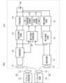
図1は第1の実施形態に係るICカード101及びICカードシステム201の構成を示すブロック図である。このICカードシステム201はICカード101とリーダライタ40とワイヤレス送電装置50とで構成される。ICカード101は、ワイヤレス送電装置50からワイヤレスで電力を受電し、またリーダライタ40と非接触で通信を行うICカードである。リーダライタ40は、リーダライタアンテナ41及びリーダライタ回路42を備える。ワイヤレス送電装置50はワイヤレス送電コイル51及びワイヤレス送電回路52を備える。ワイヤレス送電装置50は、例えば直流共鳴技術のワイヤレス給電装置や、NFC通信機能を有するスマートフォン等を充電装置として利用する場合のスマートフォンである。First Embodiment
1 is a block diagram showing the configuration of an
ワイヤレス送電回路52は、2.4GHz帯、5.7GHz帯、920MHz帯などのISMバンド(産業科学医療用バンド)の周波数帯、または6.78MHz、13.56MHzの周波数帯でワイヤレス送電コイル51に交番電力を供給する。The wireless
リーダライタ回路42は、リーダライタアンテナ41及び通信アンテナ11を介して、例えば13.56MHz帯の周波数で通信回路12と通信を行う。The reader/
ICカード101は例えば厚み0.76mmのクレジットカードサイズの電子機器である。このICカード101は、例えばカードサイズのスマートフォン(モバイル向けオペレーティングシステムを備えた携帯電話)、残高表示を行う交通系ICカード、ワンタイムパスワードカード、生体認証カード等である。ICカード101は、蓄電デバイス60を電源としてアクティブ動作したり、待機時に蓄電デバイス60をごく僅かながら電力消費したりする。また、蓄電デバイス60を電力消費しないでパッシブ動作する。The
ICカード101は、受電コイル21と、この受電コイル21に接続された受電回路20と、通信アンテナ11と、この通信アンテナ11に接続された通信回路12と、蓄電デバイス60と、受電回路20と蓄電デバイス60との間に接続された充電回路24と、通信回路12に接続された電子機能回路16と、蓄電デバイス60と電子機能回路16との間に接続された電圧変換回路15と、充電回路24及び電圧変換回路15を制御する電力供給制御回路30と、を備える。The
受電回路20は、受電コイル21に接続された受電共振キャパシタと整流平滑回路とを含む。受電コイル21と受電共振キャパシタとは共振回路を構成する。受電回路20の具体的な構成例については後に示す。
電圧変換回路23は、受電回路20の出力電圧(受電電圧)を、蓄電デバイス60の充電に要する電圧に変換する。The
充電回路制御部25は充電回路24の動作を制御する。放電制御部14は電圧変換回路15の動作を制御する。電力供給制御回路30は受電回路20から出力される電圧及び電子機能回路16から出力される通信検出信号に基づいて、充電回路制御部25及び放電制御部14へ制御信号を出力する。また、電力供給制御回路30は、受電回路20の出力電圧が所定値以上となった場合、つまり過電圧状態になったとき、受電回路20内の整流平滑回路のスイッチ素子を制御することによって整流動作を停止することで受電を遮断する。 Charging circuit control section 25 controls the operation of charging
ICカード101の概略動作は次のとおりである。 The general operation of the
[ICカード101をワイヤレス送電装置50へ載置した場合]
(a)受電コイル21はワイヤレス送電コイル51と電磁界結合し、受電回路20はワイヤレス受電する。これにより、電圧変換回路23は、受電回路20の出力電圧を、蓄電デバイス60の充電に要する電圧に変換する。[When
(a) The
(b)電力供給制御回路30は、受電回路20の出力電圧信号である受電検出信号が所定値を超えたことを検出すれば、充電回路制御部25を介して充電回路24を起動させる。これにより、充電回路24は電圧変換回路23の出力電圧で蓄電デバイス60を充電する。(b) If the power
[ICカード101をリーダライタ40へ近接させた場合]
(a)通信アンテナ11はリーダライタアンテナ41と電磁界結合し、通信回路12はリーダライタ回路42と通信する。[When the
(a) The
(b)電子機能回路16は通信回路12の動作を検出して電力供給制御回路30へ通信検出信号を出力する。(b) The
(c)電力供給制御回路30は放電制御部14を介して電圧変換回路15を起動させる。これにより、電圧変換回路15は蓄電デバイス60の電圧を電子機能回路16に要する電源電圧に変換して電子機能回路16へ出力する。(c) The power
(d)電子機能回路16は通信回路12による受電電力及び電圧変換回路15の出力電力を基に動作する。(d) The
(e)受電コイル21はリーダライタアンテナ41と電磁界結合し、受電回路20はワイヤレス受電する。これにより、電圧変換回路23は、受電回路20の出力電圧を、蓄電デバイス60の充電に要する電圧に変換する。(e) The
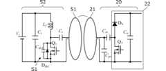
図2は、ワイヤレス給電システムに関する部分の第1の回路構成例を示す図である。この例は送電側がD級インバータ動作、受電側が直列共振、倍電圧整流動作する回路である。 FIG. 2 is a diagram showing a first circuit configuration example of a portion related to the wireless power supply system. This example is a circuit in which the power transmission side operates as a class D inverter, and the power reception side operates in series resonance and voltage doubler rectification.
ワイヤレス送電回路52は、等価的にスイッチング素子Q1、ダイオードDds1及びキャパシタCds1の並列接続回路で構成される第1スイッチ回路S1と、等価的にスイッチング素子Q2、ダイオードDds2及びキャパシタCds2の並列接続回路で構成される第2スイッチ回路S2と、スイッチング素子Q1,Q2の制御を行う図外のスイッチング制御回路と、共振キャパシタCrと、直流電源Viと、を備える。ワイヤレス送電コイル51と共振キャパシタCrとで送電共振回路が構成されている。 The wireless
スイッチング素子Q1,Q2は図外のスイッチング制御回路からの信号によってスイッチングされる。第1スイッチ回路S1のスイッチング素子Q1及び第2スイッチ回路S2のスイッチング素子Q2は交互にオン/オフされる。 Switching elements Q1 and Q2 are switched by signals from a switching control circuit (not shown). The switching element Q1 of the first switch circuit S1 and the switching element Q2 of the second switch circuit S2 are alternately turned on and off.
スイッチング素子Q1,Q2はMOSFETなどの、寄生出力容量や寄生ダイオードを有するスイッチング素子であり、スイッチ回路S1、S2を構成する。 Switching elements Q1 and Q2 are switching elements such as MOSFETs having parasitic output capacitance and parasitic diodes, and constitute switch circuits S1 and S2.
ワイヤレス送電回路52のスイッチング制御回路は第1スイッチング素子Q1及び第2スイッチング素子Q2を所定の動作周波数でスイッチングすることで、直流電圧を送電共振回路に断続的に与えて、ワイヤレス送電コイル51に共振電流を発生させる。これにより、送電コイル51に正弦波状の電流を流す。具体的には、NFC通信で用いられる13.56MHzでスイッチング動作させる。The switching control circuit of the wireless
受電回路20は、受電コイル21と共振キャパシタCrsによる受電共振回路と整流平滑回路22とを備える。整流平滑回路22は、等価的にスイッチング素子Q3、ダイオードDds3及びキャパシタCds3の並列接続回路で構成される第3スイッチ回路S3と、等価的にダイオードD4及びキャパシタCds4の並列接続回路で構成される第4スイッチ回路S4とを備える。 The
第3スイッチ回路S3及び第4スイッチ回路S4は、受電コイル21と共振キャパシタCrsによる受電共振回路に発生する電圧を整流し、キャパシタCoはその電圧を平滑する。この例では、受電コイル21と共振キャパシタCrsとは直列共振回路を構成している。 The third switch circuit S3 and the fourth switch circuit S4 rectify the voltage generated in the power receiving resonant circuit formed by the
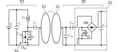
図3は、ワイヤレス給電システムに関する部分の第2の回路構成例を示す図である。この例は送電側がD級インバータ動作、受電側が並直列共振、倍電圧整流動作する回路である。送電側の構成は図2に示した例と同じである。受電側には、受電コイル21に接続された共振キャパシタCrs,Cpsを備える。受電コイル21と共振キャパシタCrsとは直列共振回路を構成していて、受電コイル21と共振キャパシタCpsとは並列共振回路を構成している。整流平滑回路22の構成は図2に示した例と同じである。 FIG. 3 is a diagram showing a second circuit configuration example of a portion related to the wireless power supply system. This example is a circuit in which the power transmission side operates as a class D inverter, and the power reception side operates in parallel series resonance and voltage doubler rectification. The configuration on the power transmission side is the same as the example shown in FIG. The power receiving side includes resonance capacitors Crs and Cps connected to the
図4は、ワイヤレス給電システムに関する部分の第3の回路構成例を示す図である。この例は送電側がD級インバータ動作、受電側が並直列共振、全波整流動作する回路である。送電側の構成は図2に示した例と同じである。受電側には、受電コイル21に接続された共振キャパシタCrs,Cpsを備える。受電コイル21と共振キャパシタCrsとは直列共振回路を構成していて、受電コイル21と共振キャパシタCpsとは並列共振回路を構成している。整流平滑回路22は、ダイオードブリッジDB、スイッチング素子Q3及びキャパシタCoで構成されている。ダイオードブリッジDBは、受電コイル21及び共振キャパシタCrs,Cpsによる受電共振回路の共振電圧を全波整流する。スイッチング素子Q3はオン状態のとき、ダイオードブリッジDBの全波整流動作を停止させ、電力受電を停止する。 FIG. 4 is a diagram showing a third circuit configuration example of a portion related to the wireless power supply system. This example is a circuit in which the power transmitting side operates as a class D inverter, and the power receiving side operates in parallel series resonance and full wave rectification. The configuration on the power transmission side is the same as the example shown in FIG. The power receiving side includes resonance capacitors Crs and Cps connected to the
図5は、ワイヤレス給電システムに関する部分の第4の回路構成例を示す図である。この例は送電側がE級インバータ動作、受電側が直列共振、E級整流動作する回路である。 FIG. 5 is a diagram showing a fourth circuit configuration example of a portion related to the wireless power supply system. This example is a circuit in which the power transmission side operates as a class E inverter, and the power receiving side operates as series resonance and class E rectification.
ワイヤレス送電回路52は、等価的にスイッチング素子Q1、ダイオードDds1及びキャパシタCds1の並列接続回路で構成される第1スイッチ回路S1と、インダクタLfと、共振キャパシタCrとを備える。ワイヤレス送電コイル51と共振キャパシタCrとで送電共振回路が構成されている。The wireless
スイッチング素子Q1は図外のスイッチング制御回路からの信号によってスイッチングされる。 The switching element Q1 is switched by a signal from a switching control circuit (not shown).
スイッチング素子Q1はMOSFETなどの、寄生出力容量や寄生ダイオードを有するスイッチング素子であり、スイッチ回路S1を構成する。Switching element Q1 is a switching element such as a MOSFET that has parasitic output capacitance and a parasitic diode, and constitutes switch circuit S1.
ワイヤレス送電回路52のスイッチング制御回路は、第1スイッチング素子Q1を所定の動作周波数でスイッチングすることで、インダクタLf、共振キャパシタCr及び送電コイル51による共振回路に直流電圧を断続的に与えて、ワイヤレス送電コイル51に共振電流を発生させる。これにより、送電コイル51に正弦波状の電流を流す。The switching control circuit of the wireless
受電回路20は、受電コイル21と共振キャパシタCrsによる受電共振回路と整流平滑回路22とを備える。整流平滑回路22は、等価的にスイッチング素子Q3、ダイオードDds3及びキャパシタCds3の並列接続回路で構成される第3スイッチ回路S3と、インダクタLfsと、平滑キャパシタCoと、を備える。The
第3スイッチ回路S3は、受電コイル21、共振キャパシタCrs及びインダクタLfsによる受電共振回路に発生する電圧を整流し、キャパシタCoはその電圧を平滑する。 The third switch circuit S3 rectifies the voltage generated in the power receiving resonant circuit formed by the
図6はワイヤレス給電システムに関する部分の第5の回路構成例を示す図である。この例は送電側がE級インバータ動作、受電側が並直列共振、倍電圧整流動作する回路である。 FIG. 6 is a diagram showing a fifth circuit configuration example of a portion related to the wireless power supply system. This example is a circuit in which the power transmission side operates as a class E inverter, and the power reception side operates in parallel series resonance and voltage doubler rectification.
ワイヤレス送電回路52の構成は図5に示した例と同様である。受電回路20の構成は図3に示した例と同様である。The configuration of the wireless
図7はワイヤレス給電システムに関する部分の第6の回路構成例を示す図である。この例は送電側がE級インバータ動作、受電側が並直列共振、全波整流動作する回路である。Figure 7 is a diagram showing a sixth circuit configuration example of the portion related to the wireless power supply system. In this example, the power transmission side operates as a class E inverter, and the power receiving side operates as a parallel-series resonance and full-wave rectification circuit.
ワイヤレス送電回路52の構成は図5に示した例と同様である。受電回路20の構成は図4に示した例と同様である。The configuration of the wireless
以上に示した例のように、ワイヤレス給電システムに関する回路は各種の構成を採り得る。As shown in the examples above, circuits related to wireless power supply systems can have a variety of configurations.
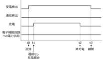
図8は、ワイヤレス送電装置50へのICカード101の載置後のICカード101の動作について示すタイムチャートである。ICカード101をワイヤレス送電装置50へ載置することによって、電力供給制御回路30がタイミングt0で受電電圧が所定値を超えたことを検出すると、その時点で通信検出信号の有無を検出する。この例では、ICカード101をワイヤレス送電装置50に載置した例であるので、通信検出信号は無い。通信検出信号が無ければ、電圧変換回路15を起動せず、電子機能回路16への電力供給を行わない。一方、t1のタイミングで直ちに充電回路24を起動して、蓄電デバイス60の充電を開始する。 FIG. 8 is a time chart showing the operation of the
その後、タイミングt3でICカード101がワイヤレス送電装置50から離されるまでに、タイミングt2で満充電状態になれば、充電を終了する。この満充電の検出及び充電の停止制御は充電回路24の制御による。 Thereafter, if the
このように、通信がなければ、電子機能回路16への電力供給を行うことなく、直ちに蓄電デバイス60への充電が開始されるので、蓄電デバイス60の充電が効率良く行われる。In this way, if there is no communication, charging of the
図9は、リーダライタ40へのICカード101の近接後のICカード101の動作について示すタイムチャートである。ICカード101をリーダライタ40へ近接させることによって、電力供給制御回路30がタイミングt0で受電電圧が所定値を超えたことを検出すると、その時点で通信検出信号の有無を検出する。この例では、ICカード101をリーダライタ40にかざした例であるので、受電を開始した後のタイミングt1で通信が検出される。通信が開始されれば、電力供給制御回路30は、充電回路24を起動することなく、つまり、蓄電デバイス60への充電が開始することなく、電圧変換回路15を起動させて、タイミングt2で電子機能回路16への電力供給を開始する。これにより、それ以降、電子機能回路16は電圧変換回路15から供給される電力で動作する。 FIG. 9 is a time chart showing the operation of the
図9に示す例では、通信が終了したことをタイミングt3で検出されると、その後のタイミングt4で電子機能回路16への電力供給を停止すると共に蓄電デバイス60への充電を開始する。その後、タイミングt5でICカード101がリーダライタ40から離されると、充電は物理的に終了する。 In the example shown in FIG. 9, when it is detected at timing t3 that the communication has ended, power supply to
このように、通信を検出すれば、充電回路24を起動することなく、電子機能回路16へ直ちに電力供給が開始されるので、速やかに通信が行われる。また、この例では通信終了後に、短時間であっても、蓄電デバイス60の充電を行うことができる。In this way, when communication is detected, power supply to the
《第2の実施形態》
第2の実施形態では、電力供給制御回路30の制御内容が、第1の実施形態で示した例とは異なるICカードについて示す。ICカードの回路構成自体は、図1に示したとおりである。《Second embodiment》
In the second embodiment, an IC card in which the control contents of the power
図10(A)はリーダライタ40へのICカード101の近接後のICカード101の動作について示すタイムチャートである。ICカード101をリーダライタ40へ近接させることによって受電すると、電力供給制御回路30は電圧変換回路15を起動する。これにより、電圧変換回路15から電子機能回路16へ電力供給が開始される。図10(A)に示す例では、タイミングt1で電子機能回路16への電力供給がなされる。その後、タイミングt2で通信検出信号の有無を検出する。通信がなければ、電力供給制御回路30は、蓄電デバイス60への充電を開始する。その後、タイミングt3でICカード101がリーダライタ40から離されると、蓄電デバイス60への充電は物理的に終了される。また、電圧変換回路15から電子機能回路16への電力供給は停止される。 FIG. 10A is a time chart showing the operation of the
図10(B)も、図10(A)に示した例と同様に、リーダライタ40へのICカード101の近接後のICカード101の動作について示すタイムチャートである。ICカード101をリーダライタ40へ近接させることによって受電すると、電圧変換回路15から電子機能回路16へ電力供給を行う。図10(B)に示す例では、タイミングt1で電子機能回路16への電力供給がなされる。その後、タイミングt2で通信検出信号の有無を検出する。通信がなければ、電力供給制御回路30は、電圧変換回路15を停止させて、電子機能回路16への電力供給を停止する。また、充電回路24を起動させて、蓄電デバイス60への充電を開始する。その後、タイミングt3でICカード101がリーダライタ40から離されると、蓄電デバイス60への充電は物理的に終了される。Figure 10 (B) is also a time chart showing the operation of the
このように、通信がなければ、電子機能回路16への電力供給を行うことなく、直ちに蓄電デバイス60への充電が開始されるので、蓄電デバイス60の充電が効率良く行われる。特に、図10(B)に示したように、通信が無いことを検出して、直ちに電子機能回路16への電力供給を停止すると、蓄電デバイス60への充電効率を高めることができる。 In this way, if there is no communication, charging of the
図11も、図10(A)、図10(B)に示した例と同様に、リーダライタ40へのICカード101の近接後のICカード101の動作について示すタイムチャートである。ICカード101をリーダライタ40へ近接させることによって受電すると、電圧変換回路15から電子機能回路16へ電力供給を行う。図11に示す例では、タイミングt1で電子機能回路16への電力供給がなされる。その後、タイミングt2で通信検出信号の有無を検出する。通信があれば、電力供給制御回路30は、充電回路24を停止させたままとし、蓄電デバイス60への充電を行わない。その後、通信が終了したことをタイミングt3で検出されると、その後のタイミングt4で電子機能回路16への電力供給を停止すると共に蓄電デバイス60への充電を開始する。その後、タイミングt5でICカード101がリーダライタ40から離されると、充電は物理的に終了する。11 is a time chart showing the operation of the
このように、受電を検出すれば、電子機能回路16へ直ちに電力が供給されるので、速やかに通信が行われる。また、通信が終了した直後に蓄電デバイス60の充電が開始されることによって、短時間であっても、蓄電デバイス60の充電を行うことができる。In this way, when the reception of power is detected, power is immediately supplied to the
最後に、本発明は上述した実施形態に限られるものではない。当業者によって適宜変形及び変更が可能である。本発明の範囲は、上述の実施形態ではなく、特許請求の範囲によって示される。さらに、本発明の範囲には、特許請求の範囲内と均等の範囲内での実施形態からの変形及び変更が含まれる。Finally, the present invention is not limited to the above-described embodiments. Appropriate modifications and changes are possible by those skilled in the art. The scope of the present invention is indicated by the claims, not by the above-described embodiments. Furthermore, the scope of the present invention includes modifications and changes from the embodiments within the scope of the claims and the scope equivalent thereto.
11…通信アンテナ
12…通信回路
14…放電制御部
15…電圧変換回路
16…電子機能回路
20…受電回路
21…受電コイル
22…整流平滑回路
23…電圧変換回路
24…充電回路
25…充電回路制御部
30…電力供給制御回路
40…リーダライタ
41…リーダライタアンテナ
42…リーダライタ回路
50…ワイヤレス送電装置
51…ワイヤレス送電コイル
52…ワイヤレス送電回路
60…蓄電デバイス
101…ICカード
201…ICカードシステム11...
Claims (12)
Translated fromJapanese受電コイルと、当該受電コイルに接続された受電回路と、通信アンテナと、当該通信アンテナに接続された通信回路と、蓄電デバイスと、前記受電回路と前記蓄電デバイスとの間に接続された充電回路と、前記通信回路に接続された電子機能回路と、前記蓄電デバイスと前記電子機能回路との間に接続された電圧変換回路と、前記充電回路及び前記電圧変換回路を制御する電力供給制御回路と、を備え、
前記電子機能回路は、前記通信回路の動作を検出して通信検出信号を出力し、
前記電力供給制御回路は、
前記受電回路の出力電圧により受電の有無を検出し、
前記電子機能回路から出力される前記通信検出信号に基づいた所定の通信の有無を検出し、
受電を検出した直後で前記蓄電デバイスへの充電を開始する前に、前記所定の通信がない場合は、前記充電回路による前記蓄電デバイスの充電を開始し、
受電を検出した直後で前記蓄電デバイスへの充電を開始する前に、前記所定の通信がある場合は、前記充電回路による前記蓄電デバイスの充電を開始せず、前記電圧変換回路から前記電子機能回路への電力供給を行う、
ICカード。 An IC card that communicates in a non-contact manner with a reader/writer that is an inductive read/write communication device,
a power receiving coil, a power receiving circuit connected to the power receiving coil, a communication antenna, a communication circuit connected to the communication antenna, a power storage device, a charging circuit connected between the power receiving circuit and the power storage device, an electronic function circuit connected to the communication circuit, a voltage conversion circuit connected between the power storage device and the electronic function circuit, and a power supply control circuit that controls the charging circuit and the voltage conversion circuit;
The electronic function circuit detects the operation of the communication circuit and outputs a communication detection signal;
The power supply control circuit includes:
Detecting whether or not power is being received based on the output voltage of the power receiving circuit;
Detecting the presence or absence of a predetermined communicationbased on the communication detection signal output from the electronic function circuit;
if there is no predetermined communication immediately after detecting reception of power andbefore starting charging of the power storage device , starting charging of the power storage device by the charging circuit;
when the predetermined communication occurs immediatelyafter detecting the reception of power and before starting charging of the power storage device , the charging circuit does not start charging the power storage device, and the voltage conversion circuit supplies power to the electronic function circuit.
IC card.
受電コイルと、当該受電コイルに接続された受電回路と、通信アンテナと、当該通信アンテナに接続された通信回路と、蓄電デバイスと、前記受電回路と前記蓄電デバイスとの間に接続された充電回路と、前記通信回路に接続された電子機能回路と、前記蓄電デバイスと前記電子機能回路との間に接続された電圧変換回路と、前記充電回路及び前記電圧変換回路を制御する電力供給制御回路と、を備え、
前記電子機能回路は、前記通信回路の動作を検出して通信検出信号を出力し、
前記電力供給制御回路は、
前記受電回路の出力電圧により受電の有無を検出し、
前記電子機能回路から出力される前記通信検出信号に基づいた所定の通信の有無を検出し、
受電により、前記電圧変換回路から前記電子機能回路への電力供給を行い、
前記蓄電デバイスへの充電を開始する前で前記所定の通信がある場合は、前記電圧変換回路から前記電子機能回路への電力供給を継続し、
前記蓄電デバイスへの充電を開始する前で前記所定の通信がない場合は、前記電圧変換回路から前記電子機能回路への電力供給を継続または停止し、前記充電回路による前記蓄電デバイスの充電を開始する、
ICカード。 An IC card that performs contactless communication with a reader/writer that is an inductive read/write communication device,
A power receiving coil, a power receiving circuit connected to the power receiving coil, a communication antenna, a communication circuit connected to the communication antenna, a power storage device, and a charging circuit connected between the power receiving circuit and the power storage device. and an electronic functional circuit connected to the communication circuit, a voltage conversion circuit connected between the electricity storage device and the electronic functional circuit, and a power supply control circuit that controls the charging circuit and the voltage conversion circuit. , comprising;
The electronic functional circuit detects the operation of the communication circuit and outputs a communication detection signal,
The power supply control circuit includes:
detecting the presence or absence of power reception based on the output voltage of the power reception circuit;
detecting the presence or absence of a predetermined communicationbased on the communication detection signal output from the electronic functional circuit;
Supplying power from the voltage conversion circuit to the electronic functional circuit by receiving power,
If there is the predetermined communicationbefore starting charging the electricity storage device , continuing power supply from the voltage conversion circuit to the electronic function circuit,
If there is no predetermined communicationbefore starting to charge the power storage device , continue or stop power supply from the voltage conversion circuit to the electronic functional circuit, and start charging the power storage device by the charging circuit. do,
IC card.
請求項1又は2に記載のICカード。 The power supply control circuit starts charging the power storage device by the charging circuit after the operation of the electronic functional circuit is completed when there is the predetermined communication.
The IC card according to claim 1 or 2.
前記電力供給制御回路は、前記充電回路が前記満充電を検知したとき、前記充電回路による前記蓄電デバイスの充電を停止する、
請求項1から3のいずれかに記載のICカード。 the charging circuit has a means for detecting whether or not a voltage of the power storage device has reached a voltage corresponding to a full charge;
the power supply control circuit stops charging of the power storage device by the charging circuit when the charging circuit detects the full charge.
4. An IC card according to claim 1.
請求項1から4のいずれかに記載のICカード。 The power supply control circuit cuts off power reception when the output voltage of the power reception circuit exceeds a predetermined value.
The IC card according to any one of claims 1 to 4.
請求項1から5のいずれかに記載のICカード。 The electronic function circuit is a fingerprint authentication circuit.
6. An IC card according to claim 1.
請求項1から6のいずれかに記載のICカード。 The power receiving circuit includes a power receiving resonance capacitor, and the power receiving resonance capacitor and the power receiving coil form a power receiving resonance mechanism.
7. An IC card according to claim 1.
請求項1から請求項7のいずれかに記載のICカード。8. An IC card according to claim 1.
ワイヤレス送電装置は、前記受電コイルと電磁界結合する送電コイルを有する、
ICカードシステム。 An IC card system comprising the IC card according to any one of claims 1 to8 , and a wireless power transmission device that wirelessly transmits power to the IC card,
The wireless power transmission device includes a power transmission coil that electromagnetically couples with the power reception coil.
IC card system.
前記リーダライタは、前記通信アンテナと電磁界結合するリーダライタアンテナを有する、the reader/writer has a reader/writer antenna that is electromagnetically coupled with the communication antenna;
請求項9に記載のICカードシステム。10. The IC card system according to claim 9.
請求項9または請求項10に記載のICカードシステム。 The power transmitting coil of the wireless power transmitting device and the power receiving coil of the IC card are coupled by an electromagnetic field in an ISM band frequency band.
The IC card system according toclaim 9 or claim 10 .
請求項9または請求項10に記載のICカードシステム。 The power transmission coil of the wireless power transmission device and the power reception coil of the IC card are coupled by an electromagnetic field in a 13.56MHz band.
The IC card system according toclaim 9 or claim 10 .
Applications Claiming Priority (3)
| Application Number | Priority Date | Filing Date | Title |
|---|---|---|---|
| JP2020096001 | 2020-06-02 | ||
| JP2020096001 | 2020-06-02 | ||
| PCT/JP2021/004027WO2021245979A1 (en) | 2020-06-02 | 2021-02-04 | Ic card and ic card system |
Publications (2)
| Publication Number | Publication Date |
|---|---|
| JPWO2021245979A1 JPWO2021245979A1 (en) | 2021-12-09 |
| JP7459940B2true JP7459940B2 (en) | 2024-04-02 |
Family
ID=78830280
Family Applications (1)
| Application Number | Title | Priority Date | Filing Date |
|---|---|---|---|
| JP2022528421AActiveJP7459940B2 (en) | 2020-06-02 | 2021-02-04 | IC card and IC card system |
Country Status (3)
| Country | Link |
|---|---|
| US (1) | US12039387B2 (en) |
| JP (1) | JP7459940B2 (en) |
| WO (1) | WO2021245979A1 (en) |
Families Citing this family (1)
| Publication number | Priority date | Publication date | Assignee | Title |
|---|---|---|---|---|
| JP7459940B2 (en)* | 2020-06-02 | 2024-04-02 | 株式会社村田製作所 | IC card and IC card system |
Citations (2)
| Publication number | Priority date | Publication date | Assignee | Title |
|---|---|---|---|---|
| JP2013211971A (en) | 2012-03-30 | 2013-10-10 | Seiko Epson Corp | Circuit device and electronic apparatus |
| JP2019115148A (en) | 2017-12-22 | 2019-07-11 | 株式会社Soken | Non-contact power reception device |
Family Cites Families (34)
| Publication number | Priority date | Publication date | Assignee | Title |
|---|---|---|---|---|
| US7904187B2 (en)* | 1999-02-01 | 2011-03-08 | Hoffberg Steven M | Internet appliance system and method |
| JP2006353042A (en)* | 2005-06-17 | 2006-12-28 | Ntt Docomo Inc | Power transmission device, power reception device, authentication / billing proxy device, charging system, power transmission method, power reception method, charging method |
| US8099140B2 (en)* | 2006-11-24 | 2012-01-17 | Semiconductor Energy Laboratory Co., Ltd. | Wireless power supply system and wireless power supply method |
| CN101635468B (en)* | 2009-09-01 | 2015-04-01 | 北京中星微电子有限公司 | Contactless charging equipment, charging method thereof, charging battery and charger |
| US20110147468A1 (en)* | 2009-12-18 | 2011-06-23 | Electronics And Telecommunications Research Institute | Rfid tag |
| JP5523388B2 (en) | 2011-05-10 | 2014-06-18 | エイエスディ株式会社 | IC card with fingerprint authentication |
| WO2014038265A1 (en)* | 2012-09-05 | 2014-03-13 | ルネサスエレクトロニクス株式会社 | Non-contact charging device, and non-contact power supply system using same |
| WO2016073202A1 (en)* | 2014-11-04 | 2016-05-12 | Intelligent Technologies International, Inc. | Smartcard |
| AU2016208989B2 (en)* | 2015-01-19 | 2021-11-25 | Royal Bank Of Canada | Secure processing of electronic payments |
| US20230045879A1 (en)* | 2015-07-15 | 2023-02-16 | Logicmark, Inc. | Preference-driven advertising systems and methods |
| US20180101718A1 (en)* | 2016-10-11 | 2018-04-12 | Zwipe As | Fingerprint authorisable device |
| US10401932B2 (en)* | 2016-12-01 | 2019-09-03 | Dell Products L.P. | Display base wireless charging pad and integrated charger control |
| US11610429B2 (en)* | 2016-12-15 | 2023-03-21 | Fingerprint Cards Anacatum Ip Ab | Fingerprint sensing module and method for manufacturing the fingerprint sensing module |
| GB2560203B (en)* | 2017-03-03 | 2021-10-27 | Zwipe As | Smartcard |
| GB2564839A (en)* | 2017-05-30 | 2019-01-30 | Zwipe As | Smartcard and method for controlling a smartcard |
| GB2563599A (en)* | 2017-06-19 | 2018-12-26 | Zwipe As | Incremental enrolment algorithm |
| US10664669B2 (en)* | 2018-01-30 | 2020-05-26 | Idex Biometrics Asa | Device architecture |
| GB2573267B (en)* | 2018-03-12 | 2023-02-15 | Idex Biometrics Asa | Power management |
| TWI686767B (en)* | 2018-02-06 | 2020-03-01 | 第一美卡事業股份有限公司 | Transaction card with fingerprint identification |
| GB2573497B (en)* | 2018-03-12 | 2022-03-30 | Idex Biometrics Asa | Device process scheduling |
| CN112203824B (en)* | 2018-06-07 | 2022-04-19 | 指纹卡安娜卡敦知识产权有限公司 | Smart card comprising a fingerprint sensor and method for manufacturing a smart card |
| GB2577477B8 (en)* | 2018-08-31 | 2022-02-16 | Idex Biometrics Asa | Biometric Interface |
| US20210081743A1 (en)* | 2019-08-12 | 2021-03-18 | Federal Card Services, LLC | Dual interface metal cards and methods of manufacturing |
| WO2021055898A1 (en)* | 2019-09-20 | 2021-03-25 | Energous Corporation | Systems and methods for machine learning based foreign object detection for wireless power transmission |
| US11398123B1 (en)* | 2019-10-10 | 2022-07-26 | Proxy, Inc. | Methods and apparatus for facilitating operation of control access systems |
| CN114902232B (en)* | 2019-12-23 | 2025-05-09 | 株式会社村田制作所 | Short-range wireless communication device |
| JP7380715B2 (en)* | 2020-01-09 | 2023-11-15 | 株式会社村田製作所 | Wireless power receiving device with short-range wireless communication function |
| JP7552682B2 (en)* | 2020-02-13 | 2024-09-18 | 株式会社村田製作所 | IC card and IC card system |
| JP7459940B2 (en)* | 2020-06-02 | 2024-04-02 | 株式会社村田製作所 | IC card and IC card system |
| DE112021001455T5 (en)* | 2020-06-05 | 2022-12-22 | Murata Manufacturing Co., Ltd. | ELECTRONIC CARD WITH BIOMETRIC AUTHENTICATION FUNCTION |
| JP7544143B2 (en)* | 2020-11-16 | 2024-09-03 | 株式会社村田製作所 | Wireless communication charging circuit system |
| FR3119058B1 (en)* | 2021-01-15 | 2023-03-31 | St Microelectronics Rousset | Management of contactless communication and contactless charging from a contactless device, and corresponding contactless device |
| CN113659731A (en)* | 2021-07-21 | 2021-11-16 | 台达电子企业管理(上海)有限公司 | Detection signal, wireless charging method and wireless charging equipment |
| CN113691024B (en)* | 2021-07-22 | 2025-01-28 | 台达电子企业管理(上海)有限公司 | Wireless charging method and wireless charging device |
- 2021
- 2021-02-04JPJP2022528421Apatent/JP7459940B2/enactiveActive
- 2021-02-04WOPCT/JP2021/004027patent/WO2021245979A1/ennot_activeCeased
- 2022
- 2022-11-29USUS18/059,774patent/US12039387B2/enactiveActive
Patent Citations (2)
| Publication number | Priority date | Publication date | Assignee | Title |
|---|---|---|---|---|
| JP2013211971A (en) | 2012-03-30 | 2013-10-10 | Seiko Epson Corp | Circuit device and electronic apparatus |
| JP2019115148A (en) | 2017-12-22 | 2019-07-11 | 株式会社Soken | Non-contact power reception device |
Also Published As
| Publication number | Publication date |
|---|---|
| JPWO2021245979A1 (en) | 2021-12-09 |
| WO2021245979A1 (en) | 2021-12-09 |
| US12039387B2 (en) | 2024-07-16 |
| US20230091589A1 (en) | 2023-03-23 |
Similar Documents
| Publication | Publication Date | Title |
|---|---|---|
| EP2966753B1 (en) | Over-voltage protection device for resonant wireless power reception device and method for controlling the over-voltage protection device | |
| EP2587613B1 (en) | Wireless power receiver for adjusting magnitude of wireless power | |
| JP6016596B2 (en) | Contactless power supply system | |
| US8583075B2 (en) | Power supply control apparatus and method thereof and mobile apparatus using the same | |
| EP2332098B1 (en) | Bidirectional wireless power transmission | |
| US8406823B2 (en) | Power transmission control device, power transmission device, power reception control device, power reception device, and electronic apparatus | |
| KR102842896B1 (en) | Device and method for wireless power transfer | |
| US9054548B2 (en) | Contactless power feeding system | |
| US20160226311A1 (en) | Power transmission device, power transmission and receiving device, method for detecting power receiving device, power receiving device detection program, and semiconductor device | |
| JPH0869513A (en) | Non-contact IC card | |
| JP7544143B2 (en) | Wireless communication charging circuit system | |
| JP2004303175A (en) | Electronic circuit for contactless tag and contactless tag | |
| CN111742323B (en) | Method for wirelessly supplying energy by means of radio frequency identification RFID and RFID system | |
| US20220383004A1 (en) | Ic card and ic card system | |
| JP7459940B2 (en) | IC card and IC card system | |
| KR101876431B1 (en) | The apparatus of smart card control with nfc chip and rfid | |
| US20230095548A1 (en) | Electronic card with biometric authentication function | |
| US11012119B2 (en) | NFC arrangement | |
| JP2007041817A (en) | RFID tag and RFID tag system | |
| KR20100120057A (en) | Noncontact type data communication and battery recharge pad for mobile phone | |
| JP2004086646A (en) | Contactless ic card | |
| CN113792563A (en) | Dual-mode radio frequency identification sensor, system and working method | |
| Lee et al. | A 48 μW, 8.88× 10− 3 W/W batteryless energy harvesting BCC identification system | |
| EP3196807B1 (en) | Smart objects | |
| GB2579587A (en) | Apparatus and method for improving wired data communication in near field RF communications enabled device with auxiliary functionality |
Legal Events
| Date | Code | Title | Description |
|---|---|---|---|
| A621 | Written request for application examination | Free format text:JAPANESE INTERMEDIATE CODE: A621 Effective date:20221003 | |
| A131 | Notification of reasons for refusal | Free format text:JAPANESE INTERMEDIATE CODE: A131 Effective date:20230815 | |
| A601 | Written request for extension of time | Free format text:JAPANESE INTERMEDIATE CODE: A601 Effective date:20231016 | |
| A521 | Request for written amendment filed | Free format text:JAPANESE INTERMEDIATE CODE: A523 Effective date:20231213 | |
| TRDD | Decision of grant or rejection written | ||
| A01 | Written decision to grant a patent or to grant a registration (utility model) | Free format text:JAPANESE INTERMEDIATE CODE: A01 Effective date:20240220 | |
| A61 | First payment of annual fees (during grant procedure) | Free format text:JAPANESE INTERMEDIATE CODE: A61 Effective date:20240304 | |
| R150 | Certificate of patent or registration of utility model | Ref document number:7459940 Country of ref document:JP Free format text:JAPANESE INTERMEDIATE CODE: R150 |