JP7458457B2 - Flowable deposition and high-density plasma processing cycle for high-quality void filling - Google Patents
Flowable deposition and high-density plasma processing cycle for high-quality void fillingDownload PDFInfo
- Publication number
- JP7458457B2 JP7458457B2JP2022171995AJP2022171995AJP7458457B2JP 7458457 B2JP7458457 B2JP 7458457B2JP 2022171995 AJP2022171995 AJP 2022171995AJP 2022171995 AJP2022171995 AJP 2022171995AJP 7458457 B2JP7458457 B2JP 7458457B2
- Authority
- JP
- Japan
- Prior art keywords
- chamber
- processing chambers
- processing
- plasma
- curing
- Prior art date
- Legal status (The legal status is an assumption and is not a legal conclusion. Google has not performed a legal analysis and makes no representation as to the accuracy of the status listed.)
- Active
Links
Images


Classifications
- H—ELECTRICITY
- H01—ELECTRIC ELEMENTS
- H01L—SEMICONDUCTOR DEVICES NOT COVERED BY CLASS H10
- H01L21/00—Processes or apparatus adapted for the manufacture or treatment of semiconductor or solid state devices or of parts thereof
- H01L21/70—Manufacture or treatment of devices consisting of a plurality of solid state components formed in or on a common substrate or of parts thereof; Manufacture of integrated circuit devices or of parts thereof
- H01L21/71—Manufacture of specific parts of devices defined in group H01L21/70
- H01L21/768—Applying interconnections to be used for carrying current between separate components within a device comprising conductors and dielectrics
- H01L21/76801—Applying interconnections to be used for carrying current between separate components within a device comprising conductors and dielectrics characterised by the formation and the after-treatment of the dielectrics, e.g. smoothing
- H01L21/76802—Applying interconnections to be used for carrying current between separate components within a device comprising conductors and dielectrics characterised by the formation and the after-treatment of the dielectrics, e.g. smoothing by forming openings in dielectrics
- H01L21/76816—Aspects relating to the layout of the pattern or to the size of vias or trenches
- H—ELECTRICITY
- H01—ELECTRIC ELEMENTS
- H01L—SEMICONDUCTOR DEVICES NOT COVERED BY CLASS H10
- H01L21/00—Processes or apparatus adapted for the manufacture or treatment of semiconductor or solid state devices or of parts thereof
- H01L21/70—Manufacture or treatment of devices consisting of a plurality of solid state components formed in or on a common substrate or of parts thereof; Manufacture of integrated circuit devices or of parts thereof
- H01L21/71—Manufacture of specific parts of devices defined in group H01L21/70
- H01L21/76—Making of isolation regions between components
- H01L21/762—Dielectric regions, e.g. EPIC dielectric isolation, LOCOS; Trench refilling techniques, SOI technology, use of channel stoppers
- H01L21/76224—Dielectric regions, e.g. EPIC dielectric isolation, LOCOS; Trench refilling techniques, SOI technology, use of channel stoppers using trench refilling with dielectric materials
- H—ELECTRICITY
- H01—ELECTRIC ELEMENTS
- H01L—SEMICONDUCTOR DEVICES NOT COVERED BY CLASS H10
- H01L21/00—Processes or apparatus adapted for the manufacture or treatment of semiconductor or solid state devices or of parts thereof
- H01L21/67—Apparatus specially adapted for handling semiconductor or electric solid state devices during manufacture or treatment thereof; Apparatus specially adapted for handling wafers during manufacture or treatment of semiconductor or electric solid state devices or components ; Apparatus not specifically provided for elsewhere
- H01L21/67005—Apparatus not specifically provided for elsewhere
- H01L21/67011—Apparatus for manufacture or treatment
- H01L21/67155—Apparatus for manufacturing or treating in a plurality of work-stations
- H01L21/67207—Apparatus for manufacturing or treating in a plurality of work-stations comprising a chamber adapted to a particular process
- C—CHEMISTRY; METALLURGY
- C23—COATING METALLIC MATERIAL; COATING MATERIAL WITH METALLIC MATERIAL; CHEMICAL SURFACE TREATMENT; DIFFUSION TREATMENT OF METALLIC MATERIAL; COATING BY VACUUM EVAPORATION, BY SPUTTERING, BY ION IMPLANTATION OR BY CHEMICAL VAPOUR DEPOSITION, IN GENERAL; INHIBITING CORROSION OF METALLIC MATERIAL OR INCRUSTATION IN GENERAL
- C23C—COATING METALLIC MATERIAL; COATING MATERIAL WITH METALLIC MATERIAL; SURFACE TREATMENT OF METALLIC MATERIAL BY DIFFUSION INTO THE SURFACE, BY CHEMICAL CONVERSION OR SUBSTITUTION; COATING BY VACUUM EVAPORATION, BY SPUTTERING, BY ION IMPLANTATION OR BY CHEMICAL VAPOUR DEPOSITION, IN GENERAL
- C23C16/00—Chemical coating by decomposition of gaseous compounds, without leaving reaction products of surface material in the coating, i.e. chemical vapour deposition [CVD] processes
- C23C16/04—Coating on selected surface areas, e.g. using masks
- C23C16/045—Coating cavities or hollow spaces, e.g. interior of tubes; Infiltration of porous substrates
- C—CHEMISTRY; METALLURGY
- C23—COATING METALLIC MATERIAL; COATING MATERIAL WITH METALLIC MATERIAL; CHEMICAL SURFACE TREATMENT; DIFFUSION TREATMENT OF METALLIC MATERIAL; COATING BY VACUUM EVAPORATION, BY SPUTTERING, BY ION IMPLANTATION OR BY CHEMICAL VAPOUR DEPOSITION, IN GENERAL; INHIBITING CORROSION OF METALLIC MATERIAL OR INCRUSTATION IN GENERAL
- C23C—COATING METALLIC MATERIAL; COATING MATERIAL WITH METALLIC MATERIAL; SURFACE TREATMENT OF METALLIC MATERIAL BY DIFFUSION INTO THE SURFACE, BY CHEMICAL CONVERSION OR SUBSTITUTION; COATING BY VACUUM EVAPORATION, BY SPUTTERING, BY ION IMPLANTATION OR BY CHEMICAL VAPOUR DEPOSITION, IN GENERAL
- C23C16/00—Chemical coating by decomposition of gaseous compounds, without leaving reaction products of surface material in the coating, i.e. chemical vapour deposition [CVD] processes
- C23C16/22—Chemical coating by decomposition of gaseous compounds, without leaving reaction products of surface material in the coating, i.e. chemical vapour deposition [CVD] processes characterised by the deposition of inorganic material, other than metallic material
- C23C16/30—Deposition of compounds, mixtures or solid solutions, e.g. borides, carbides, nitrides
- C23C16/308—Oxynitrides
- C—CHEMISTRY; METALLURGY
- C23—COATING METALLIC MATERIAL; COATING MATERIAL WITH METALLIC MATERIAL; CHEMICAL SURFACE TREATMENT; DIFFUSION TREATMENT OF METALLIC MATERIAL; COATING BY VACUUM EVAPORATION, BY SPUTTERING, BY ION IMPLANTATION OR BY CHEMICAL VAPOUR DEPOSITION, IN GENERAL; INHIBITING CORROSION OF METALLIC MATERIAL OR INCRUSTATION IN GENERAL
- C23C—COATING METALLIC MATERIAL; COATING MATERIAL WITH METALLIC MATERIAL; SURFACE TREATMENT OF METALLIC MATERIAL BY DIFFUSION INTO THE SURFACE, BY CHEMICAL CONVERSION OR SUBSTITUTION; COATING BY VACUUM EVAPORATION, BY SPUTTERING, BY ION IMPLANTATION OR BY CHEMICAL VAPOUR DEPOSITION, IN GENERAL
- C23C16/00—Chemical coating by decomposition of gaseous compounds, without leaving reaction products of surface material in the coating, i.e. chemical vapour deposition [CVD] processes
- C23C16/22—Chemical coating by decomposition of gaseous compounds, without leaving reaction products of surface material in the coating, i.e. chemical vapour deposition [CVD] processes characterised by the deposition of inorganic material, other than metallic material
- C23C16/30—Deposition of compounds, mixtures or solid solutions, e.g. borides, carbides, nitrides
- C23C16/32—Carbides
- C23C16/325—Silicon carbide
- C—CHEMISTRY; METALLURGY
- C23—COATING METALLIC MATERIAL; COATING MATERIAL WITH METALLIC MATERIAL; CHEMICAL SURFACE TREATMENT; DIFFUSION TREATMENT OF METALLIC MATERIAL; COATING BY VACUUM EVAPORATION, BY SPUTTERING, BY ION IMPLANTATION OR BY CHEMICAL VAPOUR DEPOSITION, IN GENERAL; INHIBITING CORROSION OF METALLIC MATERIAL OR INCRUSTATION IN GENERAL
- C23C—COATING METALLIC MATERIAL; COATING MATERIAL WITH METALLIC MATERIAL; SURFACE TREATMENT OF METALLIC MATERIAL BY DIFFUSION INTO THE SURFACE, BY CHEMICAL CONVERSION OR SUBSTITUTION; COATING BY VACUUM EVAPORATION, BY SPUTTERING, BY ION IMPLANTATION OR BY CHEMICAL VAPOUR DEPOSITION, IN GENERAL
- C23C16/00—Chemical coating by decomposition of gaseous compounds, without leaving reaction products of surface material in the coating, i.e. chemical vapour deposition [CVD] processes
- C23C16/22—Chemical coating by decomposition of gaseous compounds, without leaving reaction products of surface material in the coating, i.e. chemical vapour deposition [CVD] processes characterised by the deposition of inorganic material, other than metallic material
- C23C16/30—Deposition of compounds, mixtures or solid solutions, e.g. borides, carbides, nitrides
- C23C16/34—Nitrides
- C23C16/345—Silicon nitride
- C—CHEMISTRY; METALLURGY
- C23—COATING METALLIC MATERIAL; COATING MATERIAL WITH METALLIC MATERIAL; CHEMICAL SURFACE TREATMENT; DIFFUSION TREATMENT OF METALLIC MATERIAL; COATING BY VACUUM EVAPORATION, BY SPUTTERING, BY ION IMPLANTATION OR BY CHEMICAL VAPOUR DEPOSITION, IN GENERAL; INHIBITING CORROSION OF METALLIC MATERIAL OR INCRUSTATION IN GENERAL
- C23C—COATING METALLIC MATERIAL; COATING MATERIAL WITH METALLIC MATERIAL; SURFACE TREATMENT OF METALLIC MATERIAL BY DIFFUSION INTO THE SURFACE, BY CHEMICAL CONVERSION OR SUBSTITUTION; COATING BY VACUUM EVAPORATION, BY SPUTTERING, BY ION IMPLANTATION OR BY CHEMICAL VAPOUR DEPOSITION, IN GENERAL
- C23C16/00—Chemical coating by decomposition of gaseous compounds, without leaving reaction products of surface material in the coating, i.e. chemical vapour deposition [CVD] processes
- C23C16/22—Chemical coating by decomposition of gaseous compounds, without leaving reaction products of surface material in the coating, i.e. chemical vapour deposition [CVD] processes characterised by the deposition of inorganic material, other than metallic material
- C23C16/30—Deposition of compounds, mixtures or solid solutions, e.g. borides, carbides, nitrides
- C23C16/36—Carbonitrides
- C—CHEMISTRY; METALLURGY
- C23—COATING METALLIC MATERIAL; COATING MATERIAL WITH METALLIC MATERIAL; CHEMICAL SURFACE TREATMENT; DIFFUSION TREATMENT OF METALLIC MATERIAL; COATING BY VACUUM EVAPORATION, BY SPUTTERING, BY ION IMPLANTATION OR BY CHEMICAL VAPOUR DEPOSITION, IN GENERAL; INHIBITING CORROSION OF METALLIC MATERIAL OR INCRUSTATION IN GENERAL
- C23C—COATING METALLIC MATERIAL; COATING MATERIAL WITH METALLIC MATERIAL; SURFACE TREATMENT OF METALLIC MATERIAL BY DIFFUSION INTO THE SURFACE, BY CHEMICAL CONVERSION OR SUBSTITUTION; COATING BY VACUUM EVAPORATION, BY SPUTTERING, BY ION IMPLANTATION OR BY CHEMICAL VAPOUR DEPOSITION, IN GENERAL
- C23C16/00—Chemical coating by decomposition of gaseous compounds, without leaving reaction products of surface material in the coating, i.e. chemical vapour deposition [CVD] processes
- C23C16/22—Chemical coating by decomposition of gaseous compounds, without leaving reaction products of surface material in the coating, i.e. chemical vapour deposition [CVD] processes characterised by the deposition of inorganic material, other than metallic material
- C23C16/30—Deposition of compounds, mixtures or solid solutions, e.g. borides, carbides, nitrides
- C23C16/40—Oxides
- C23C16/401—Oxides containing silicon
- C23C16/402—Silicon dioxide
- C—CHEMISTRY; METALLURGY
- C23—COATING METALLIC MATERIAL; COATING MATERIAL WITH METALLIC MATERIAL; CHEMICAL SURFACE TREATMENT; DIFFUSION TREATMENT OF METALLIC MATERIAL; COATING BY VACUUM EVAPORATION, BY SPUTTERING, BY ION IMPLANTATION OR BY CHEMICAL VAPOUR DEPOSITION, IN GENERAL; INHIBITING CORROSION OF METALLIC MATERIAL OR INCRUSTATION IN GENERAL
- C23C—COATING METALLIC MATERIAL; COATING MATERIAL WITH METALLIC MATERIAL; SURFACE TREATMENT OF METALLIC MATERIAL BY DIFFUSION INTO THE SURFACE, BY CHEMICAL CONVERSION OR SUBSTITUTION; COATING BY VACUUM EVAPORATION, BY SPUTTERING, BY ION IMPLANTATION OR BY CHEMICAL VAPOUR DEPOSITION, IN GENERAL
- C23C16/00—Chemical coating by decomposition of gaseous compounds, without leaving reaction products of surface material in the coating, i.e. chemical vapour deposition [CVD] processes
- C23C16/44—Chemical coating by decomposition of gaseous compounds, without leaving reaction products of surface material in the coating, i.e. chemical vapour deposition [CVD] processes characterised by the method of coating
- C23C16/455—Chemical coating by decomposition of gaseous compounds, without leaving reaction products of surface material in the coating, i.e. chemical vapour deposition [CVD] processes characterised by the method of coating characterised by the method used for introducing gases into reaction chamber or for modifying gas flows in reaction chamber
- C23C16/45523—Pulsed gas flow or change of composition over time
- C23C16/45525—Atomic layer deposition [ALD]
- C23C16/45527—Atomic layer deposition [ALD] characterized by the ALD cycle, e.g. different flows or temperatures during half-reactions, unusual pulsing sequence, use of precursor mixtures or auxiliary reactants or activations
- C23C16/45536—Use of plasma, radiation or electromagnetic fields
- C23C16/4554—Plasma being used non-continuously in between ALD reactions
- C—CHEMISTRY; METALLURGY
- C23—COATING METALLIC MATERIAL; COATING MATERIAL WITH METALLIC MATERIAL; CHEMICAL SURFACE TREATMENT; DIFFUSION TREATMENT OF METALLIC MATERIAL; COATING BY VACUUM EVAPORATION, BY SPUTTERING, BY ION IMPLANTATION OR BY CHEMICAL VAPOUR DEPOSITION, IN GENERAL; INHIBITING CORROSION OF METALLIC MATERIAL OR INCRUSTATION IN GENERAL
- C23C—COATING METALLIC MATERIAL; COATING MATERIAL WITH METALLIC MATERIAL; SURFACE TREATMENT OF METALLIC MATERIAL BY DIFFUSION INTO THE SURFACE, BY CHEMICAL CONVERSION OR SUBSTITUTION; COATING BY VACUUM EVAPORATION, BY SPUTTERING, BY ION IMPLANTATION OR BY CHEMICAL VAPOUR DEPOSITION, IN GENERAL
- C23C16/00—Chemical coating by decomposition of gaseous compounds, without leaving reaction products of surface material in the coating, i.e. chemical vapour deposition [CVD] processes
- C23C16/44—Chemical coating by decomposition of gaseous compounds, without leaving reaction products of surface material in the coating, i.e. chemical vapour deposition [CVD] processes characterised by the method of coating
- C23C16/50—Chemical coating by decomposition of gaseous compounds, without leaving reaction products of surface material in the coating, i.e. chemical vapour deposition [CVD] processes characterised by the method of coating using electric discharges
- C23C16/505—Chemical coating by decomposition of gaseous compounds, without leaving reaction products of surface material in the coating, i.e. chemical vapour deposition [CVD] processes characterised by the method of coating using electric discharges using radio frequency discharges
- C—CHEMISTRY; METALLURGY
- C23—COATING METALLIC MATERIAL; COATING MATERIAL WITH METALLIC MATERIAL; CHEMICAL SURFACE TREATMENT; DIFFUSION TREATMENT OF METALLIC MATERIAL; COATING BY VACUUM EVAPORATION, BY SPUTTERING, BY ION IMPLANTATION OR BY CHEMICAL VAPOUR DEPOSITION, IN GENERAL; INHIBITING CORROSION OF METALLIC MATERIAL OR INCRUSTATION IN GENERAL
- C23C—COATING METALLIC MATERIAL; COATING MATERIAL WITH METALLIC MATERIAL; SURFACE TREATMENT OF METALLIC MATERIAL BY DIFFUSION INTO THE SURFACE, BY CHEMICAL CONVERSION OR SUBSTITUTION; COATING BY VACUUM EVAPORATION, BY SPUTTERING, BY ION IMPLANTATION OR BY CHEMICAL VAPOUR DEPOSITION, IN GENERAL
- C23C16/00—Chemical coating by decomposition of gaseous compounds, without leaving reaction products of surface material in the coating, i.e. chemical vapour deposition [CVD] processes
- C23C16/56—After-treatment
- H—ELECTRICITY
- H01—ELECTRIC ELEMENTS
- H01J—ELECTRIC DISCHARGE TUBES OR DISCHARGE LAMPS
- H01J37/00—Discharge tubes with provision for introducing objects or material to be exposed to the discharge, e.g. for the purpose of examination or processing thereof
- H01J37/32—Gas-filled discharge tubes
- H01J37/32431—Constructional details of the reactor
- H01J37/32798—Further details of plasma apparatus not provided for in groups H01J37/3244 - H01J37/32788; special provisions for cleaning or maintenance of the apparatus
- H01J37/32899—Multiple chambers, e.g. cluster tools
- H—ELECTRICITY
- H01—ELECTRIC ELEMENTS
- H01L—SEMICONDUCTOR DEVICES NOT COVERED BY CLASS H10
- H01L21/00—Processes or apparatus adapted for the manufacture or treatment of semiconductor or solid state devices or of parts thereof
- H01L21/02—Manufacture or treatment of semiconductor devices or of parts thereof
- H01L21/02104—Forming layers
- H01L21/02107—Forming insulating materials on a substrate
- H01L21/02109—Forming insulating materials on a substrate characterised by the type of layer, e.g. type of material, porous/non-porous, pre-cursors, mixtures or laminates
- H01L21/02112—Forming insulating materials on a substrate characterised by the type of layer, e.g. type of material, porous/non-porous, pre-cursors, mixtures or laminates characterised by the material of the layer
- H01L21/02123—Forming insulating materials on a substrate characterised by the type of layer, e.g. type of material, porous/non-porous, pre-cursors, mixtures or laminates characterised by the material of the layer the material containing silicon
- H01L21/02126—Forming insulating materials on a substrate characterised by the type of layer, e.g. type of material, porous/non-porous, pre-cursors, mixtures or laminates characterised by the material of the layer the material containing silicon the material containing Si, O, and at least one of H, N, C, F, or other non-metal elements, e.g. SiOC, SiOC:H or SiONC
- H01L21/0214—Forming insulating materials on a substrate characterised by the type of layer, e.g. type of material, porous/non-porous, pre-cursors, mixtures or laminates characterised by the material of the layer the material containing silicon the material containing Si, O, and at least one of H, N, C, F, or other non-metal elements, e.g. SiOC, SiOC:H or SiONC the material being a silicon oxynitride, e.g. SiON or SiON:H
- H—ELECTRICITY
- H01—ELECTRIC ELEMENTS
- H01L—SEMICONDUCTOR DEVICES NOT COVERED BY CLASS H10
- H01L21/00—Processes or apparatus adapted for the manufacture or treatment of semiconductor or solid state devices or of parts thereof
- H01L21/02—Manufacture or treatment of semiconductor devices or of parts thereof
- H01L21/02104—Forming layers
- H01L21/02107—Forming insulating materials on a substrate
- H01L21/02109—Forming insulating materials on a substrate characterised by the type of layer, e.g. type of material, porous/non-porous, pre-cursors, mixtures or laminates
- H01L21/02112—Forming insulating materials on a substrate characterised by the type of layer, e.g. type of material, porous/non-porous, pre-cursors, mixtures or laminates characterised by the material of the layer
- H01L21/02123—Forming insulating materials on a substrate characterised by the type of layer, e.g. type of material, porous/non-porous, pre-cursors, mixtures or laminates characterised by the material of the layer the material containing silicon
- H01L21/02164—Forming insulating materials on a substrate characterised by the type of layer, e.g. type of material, porous/non-porous, pre-cursors, mixtures or laminates characterised by the material of the layer the material containing silicon the material being a silicon oxide, e.g. SiO2
- H—ELECTRICITY
- H01—ELECTRIC ELEMENTS
- H01L—SEMICONDUCTOR DEVICES NOT COVERED BY CLASS H10
- H01L21/00—Processes or apparatus adapted for the manufacture or treatment of semiconductor or solid state devices or of parts thereof
- H01L21/02—Manufacture or treatment of semiconductor devices or of parts thereof
- H01L21/02104—Forming layers
- H01L21/02107—Forming insulating materials on a substrate
- H01L21/02109—Forming insulating materials on a substrate characterised by the type of layer, e.g. type of material, porous/non-porous, pre-cursors, mixtures or laminates
- H01L21/02112—Forming insulating materials on a substrate characterised by the type of layer, e.g. type of material, porous/non-porous, pre-cursors, mixtures or laminates characterised by the material of the layer
- H01L21/02123—Forming insulating materials on a substrate characterised by the type of layer, e.g. type of material, porous/non-porous, pre-cursors, mixtures or laminates characterised by the material of the layer the material containing silicon
- H01L21/02167—Forming insulating materials on a substrate characterised by the type of layer, e.g. type of material, porous/non-porous, pre-cursors, mixtures or laminates characterised by the material of the layer the material containing silicon the material being a silicon carbide not containing oxygen, e.g. SiC, SiC:H or silicon carbonitrides
- H—ELECTRICITY
- H01—ELECTRIC ELEMENTS
- H01L—SEMICONDUCTOR DEVICES NOT COVERED BY CLASS H10
- H01L21/00—Processes or apparatus adapted for the manufacture or treatment of semiconductor or solid state devices or of parts thereof
- H01L21/02—Manufacture or treatment of semiconductor devices or of parts thereof
- H01L21/02104—Forming layers
- H01L21/02107—Forming insulating materials on a substrate
- H01L21/02109—Forming insulating materials on a substrate characterised by the type of layer, e.g. type of material, porous/non-porous, pre-cursors, mixtures or laminates
- H01L21/02112—Forming insulating materials on a substrate characterised by the type of layer, e.g. type of material, porous/non-porous, pre-cursors, mixtures or laminates characterised by the material of the layer
- H01L21/02123—Forming insulating materials on a substrate characterised by the type of layer, e.g. type of material, porous/non-porous, pre-cursors, mixtures or laminates characterised by the material of the layer the material containing silicon
- H01L21/0217—Forming insulating materials on a substrate characterised by the type of layer, e.g. type of material, porous/non-porous, pre-cursors, mixtures or laminates characterised by the material of the layer the material containing silicon the material being a silicon nitride not containing oxygen, e.g. SixNy or SixByNz
- H—ELECTRICITY
- H01—ELECTRIC ELEMENTS
- H01L—SEMICONDUCTOR DEVICES NOT COVERED BY CLASS H10
- H01L21/00—Processes or apparatus adapted for the manufacture or treatment of semiconductor or solid state devices or of parts thereof
- H01L21/02—Manufacture or treatment of semiconductor devices or of parts thereof
- H01L21/02104—Forming layers
- H01L21/02107—Forming insulating materials on a substrate
- H01L21/02109—Forming insulating materials on a substrate characterised by the type of layer, e.g. type of material, porous/non-porous, pre-cursors, mixtures or laminates
- H01L21/02205—Forming insulating materials on a substrate characterised by the type of layer, e.g. type of material, porous/non-porous, pre-cursors, mixtures or laminates the layer being characterised by the precursor material for deposition
- H01L21/02208—Forming insulating materials on a substrate characterised by the type of layer, e.g. type of material, porous/non-porous, pre-cursors, mixtures or laminates the layer being characterised by the precursor material for deposition the precursor containing a compound comprising Si
- H01L21/02211—Forming insulating materials on a substrate characterised by the type of layer, e.g. type of material, porous/non-porous, pre-cursors, mixtures or laminates the layer being characterised by the precursor material for deposition the precursor containing a compound comprising Si the compound being a silane, e.g. disilane, methylsilane or chlorosilane
- H—ELECTRICITY
- H01—ELECTRIC ELEMENTS
- H01L—SEMICONDUCTOR DEVICES NOT COVERED BY CLASS H10
- H01L21/00—Processes or apparatus adapted for the manufacture or treatment of semiconductor or solid state devices or of parts thereof
- H01L21/02—Manufacture or treatment of semiconductor devices or of parts thereof
- H01L21/02104—Forming layers
- H01L21/02107—Forming insulating materials on a substrate
- H01L21/02109—Forming insulating materials on a substrate characterised by the type of layer, e.g. type of material, porous/non-porous, pre-cursors, mixtures or laminates
- H01L21/02205—Forming insulating materials on a substrate characterised by the type of layer, e.g. type of material, porous/non-porous, pre-cursors, mixtures or laminates the layer being characterised by the precursor material for deposition
- H01L21/02208—Forming insulating materials on a substrate characterised by the type of layer, e.g. type of material, porous/non-porous, pre-cursors, mixtures or laminates the layer being characterised by the precursor material for deposition the precursor containing a compound comprising Si
- H01L21/02214—Forming insulating materials on a substrate characterised by the type of layer, e.g. type of material, porous/non-porous, pre-cursors, mixtures or laminates the layer being characterised by the precursor material for deposition the precursor containing a compound comprising Si the compound comprising silicon and oxygen
- H01L21/02216—Forming insulating materials on a substrate characterised by the type of layer, e.g. type of material, porous/non-porous, pre-cursors, mixtures or laminates the layer being characterised by the precursor material for deposition the precursor containing a compound comprising Si the compound comprising silicon and oxygen the compound being a molecule comprising at least one silicon-oxygen bond and the compound having hydrogen or an organic group attached to the silicon or oxygen, e.g. a siloxane
- H—ELECTRICITY
- H01—ELECTRIC ELEMENTS
- H01L—SEMICONDUCTOR DEVICES NOT COVERED BY CLASS H10
- H01L21/00—Processes or apparatus adapted for the manufacture or treatment of semiconductor or solid state devices or of parts thereof
- H01L21/02—Manufacture or treatment of semiconductor devices or of parts thereof
- H01L21/02104—Forming layers
- H01L21/02107—Forming insulating materials on a substrate
- H01L21/02109—Forming insulating materials on a substrate characterised by the type of layer, e.g. type of material, porous/non-porous, pre-cursors, mixtures or laminates
- H01L21/02205—Forming insulating materials on a substrate characterised by the type of layer, e.g. type of material, porous/non-porous, pre-cursors, mixtures or laminates the layer being characterised by the precursor material for deposition
- H01L21/02208—Forming insulating materials on a substrate characterised by the type of layer, e.g. type of material, porous/non-porous, pre-cursors, mixtures or laminates the layer being characterised by the precursor material for deposition the precursor containing a compound comprising Si
- H01L21/02219—Forming insulating materials on a substrate characterised by the type of layer, e.g. type of material, porous/non-porous, pre-cursors, mixtures or laminates the layer being characterised by the precursor material for deposition the precursor containing a compound comprising Si the compound comprising silicon and nitrogen
- H—ELECTRICITY
- H01—ELECTRIC ELEMENTS
- H01L—SEMICONDUCTOR DEVICES NOT COVERED BY CLASS H10
- H01L21/00—Processes or apparatus adapted for the manufacture or treatment of semiconductor or solid state devices or of parts thereof
- H01L21/02—Manufacture or treatment of semiconductor devices or of parts thereof
- H01L21/02104—Forming layers
- H01L21/02107—Forming insulating materials on a substrate
- H01L21/02225—Forming insulating materials on a substrate characterised by the process for the formation of the insulating layer
- H01L21/0226—Forming insulating materials on a substrate characterised by the process for the formation of the insulating layer formation by a deposition process
- H01L21/02263—Forming insulating materials on a substrate characterised by the process for the formation of the insulating layer formation by a deposition process deposition from the gas or vapour phase
- H01L21/02271—Forming insulating materials on a substrate characterised by the process for the formation of the insulating layer formation by a deposition process deposition from the gas or vapour phase deposition by decomposition or reaction of gaseous or vapour phase compounds, i.e. chemical vapour deposition
- H01L21/02274—Forming insulating materials on a substrate characterised by the process for the formation of the insulating layer formation by a deposition process deposition from the gas or vapour phase deposition by decomposition or reaction of gaseous or vapour phase compounds, i.e. chemical vapour deposition in the presence of a plasma [PECVD]
- H—ELECTRICITY
- H01—ELECTRIC ELEMENTS
- H01L—SEMICONDUCTOR DEVICES NOT COVERED BY CLASS H10
- H01L21/00—Processes or apparatus adapted for the manufacture or treatment of semiconductor or solid state devices or of parts thereof
- H01L21/02—Manufacture or treatment of semiconductor devices or of parts thereof
- H01L21/02104—Forming layers
- H01L21/02107—Forming insulating materials on a substrate
- H01L21/02225—Forming insulating materials on a substrate characterised by the process for the formation of the insulating layer
- H01L21/0226—Forming insulating materials on a substrate characterised by the process for the formation of the insulating layer formation by a deposition process
- H01L21/02263—Forming insulating materials on a substrate characterised by the process for the formation of the insulating layer formation by a deposition process deposition from the gas or vapour phase
- H01L21/02271—Forming insulating materials on a substrate characterised by the process for the formation of the insulating layer formation by a deposition process deposition from the gas or vapour phase deposition by decomposition or reaction of gaseous or vapour phase compounds, i.e. chemical vapour deposition
- H01L21/0228—Forming insulating materials on a substrate characterised by the process for the formation of the insulating layer formation by a deposition process deposition from the gas or vapour phase deposition by decomposition or reaction of gaseous or vapour phase compounds, i.e. chemical vapour deposition deposition by cyclic CVD, e.g. ALD, ALE, pulsed CVD
- H—ELECTRICITY
- H01—ELECTRIC ELEMENTS
- H01L—SEMICONDUCTOR DEVICES NOT COVERED BY CLASS H10
- H01L21/00—Processes or apparatus adapted for the manufacture or treatment of semiconductor or solid state devices or of parts thereof
- H01L21/02—Manufacture or treatment of semiconductor devices or of parts thereof
- H01L21/02104—Forming layers
- H01L21/02107—Forming insulating materials on a substrate
- H01L21/02296—Forming insulating materials on a substrate characterised by the treatment performed before or after the formation of the layer
- H01L21/02318—Forming insulating materials on a substrate characterised by the treatment performed before or after the formation of the layer post-treatment
- H01L21/02321—Forming insulating materials on a substrate characterised by the treatment performed before or after the formation of the layer post-treatment introduction of substances into an already existing insulating layer
- H01L21/02323—Forming insulating materials on a substrate characterised by the treatment performed before or after the formation of the layer post-treatment introduction of substances into an already existing insulating layer introduction of oxygen
- H01L21/02326—Forming insulating materials on a substrate characterised by the treatment performed before or after the formation of the layer post-treatment introduction of substances into an already existing insulating layer introduction of oxygen into a nitride layer, e.g. changing SiN to SiON
- H—ELECTRICITY
- H01—ELECTRIC ELEMENTS
- H01L—SEMICONDUCTOR DEVICES NOT COVERED BY CLASS H10
- H01L21/00—Processes or apparatus adapted for the manufacture or treatment of semiconductor or solid state devices or of parts thereof
- H01L21/02—Manufacture or treatment of semiconductor devices or of parts thereof
- H01L21/02104—Forming layers
- H01L21/02107—Forming insulating materials on a substrate
- H01L21/02296—Forming insulating materials on a substrate characterised by the treatment performed before or after the formation of the layer
- H01L21/02318—Forming insulating materials on a substrate characterised by the treatment performed before or after the formation of the layer post-treatment
- H01L21/02321—Forming insulating materials on a substrate characterised by the treatment performed before or after the formation of the layer post-treatment introduction of substances into an already existing insulating layer
- H01L21/02329—Forming insulating materials on a substrate characterised by the treatment performed before or after the formation of the layer post-treatment introduction of substances into an already existing insulating layer introduction of nitrogen
- H—ELECTRICITY
- H01—ELECTRIC ELEMENTS
- H01L—SEMICONDUCTOR DEVICES NOT COVERED BY CLASS H10
- H01L21/00—Processes or apparatus adapted for the manufacture or treatment of semiconductor or solid state devices or of parts thereof
- H01L21/02—Manufacture or treatment of semiconductor devices or of parts thereof
- H01L21/02104—Forming layers
- H01L21/02107—Forming insulating materials on a substrate
- H01L21/02296—Forming insulating materials on a substrate characterised by the treatment performed before or after the formation of the layer
- H01L21/02318—Forming insulating materials on a substrate characterised by the treatment performed before or after the formation of the layer post-treatment
- H01L21/02337—Forming insulating materials on a substrate characterised by the treatment performed before or after the formation of the layer post-treatment treatment by exposure to a gas or vapour
- H01L21/0234—Forming insulating materials on a substrate characterised by the treatment performed before or after the formation of the layer post-treatment treatment by exposure to a gas or vapour treatment by exposure to a plasma
- H—ELECTRICITY
- H01—ELECTRIC ELEMENTS
- H01L—SEMICONDUCTOR DEVICES NOT COVERED BY CLASS H10
- H01L21/00—Processes or apparatus adapted for the manufacture or treatment of semiconductor or solid state devices or of parts thereof
- H01L21/02—Manufacture or treatment of semiconductor devices or of parts thereof
- H01L21/02104—Forming layers
- H01L21/02107—Forming insulating materials on a substrate
- H01L21/02296—Forming insulating materials on a substrate characterised by the treatment performed before or after the formation of the layer
- H01L21/02318—Forming insulating materials on a substrate characterised by the treatment performed before or after the formation of the layer post-treatment
- H01L21/02345—Forming insulating materials on a substrate characterised by the treatment performed before or after the formation of the layer post-treatment treatment by exposure to radiation, e.g. visible light
- H01L21/02348—Forming insulating materials on a substrate characterised by the treatment performed before or after the formation of the layer post-treatment treatment by exposure to radiation, e.g. visible light treatment by exposure to UV light
- H—ELECTRICITY
- H01—ELECTRIC ELEMENTS
- H01L—SEMICONDUCTOR DEVICES NOT COVERED BY CLASS H10
- H01L21/00—Processes or apparatus adapted for the manufacture or treatment of semiconductor or solid state devices or of parts thereof
- H01L21/02—Manufacture or treatment of semiconductor devices or of parts thereof
- H01L21/027—Making masks on semiconductor bodies for further photolithographic processing not provided for in group H01L21/18 or H01L21/34
- H01L21/0271—Making masks on semiconductor bodies for further photolithographic processing not provided for in group H01L21/18 or H01L21/34 comprising organic layers
- H01L21/0273—Making masks on semiconductor bodies for further photolithographic processing not provided for in group H01L21/18 or H01L21/34 comprising organic layers characterised by the treatment of photoresist layers
- H01L21/0274—Photolithographic processes
- H—ELECTRICITY
- H01—ELECTRIC ELEMENTS
- H01L—SEMICONDUCTOR DEVICES NOT COVERED BY CLASS H10
- H01L21/00—Processes or apparatus adapted for the manufacture or treatment of semiconductor or solid state devices or of parts thereof
- H01L21/67—Apparatus specially adapted for handling semiconductor or electric solid state devices during manufacture or treatment thereof; Apparatus specially adapted for handling wafers during manufacture or treatment of semiconductor or electric solid state devices or components ; Apparatus not specifically provided for elsewhere
- H01L21/67005—Apparatus not specifically provided for elsewhere
- H01L21/67011—Apparatus for manufacture or treatment
- H01L21/67155—Apparatus for manufacturing or treating in a plurality of work-stations
- H01L21/67161—Apparatus for manufacturing or treating in a plurality of work-stations characterized by the layout of the process chambers
- H01L21/67167—Apparatus for manufacturing or treating in a plurality of work-stations characterized by the layout of the process chambers surrounding a central transfer chamber
- H—ELECTRICITY
- H01—ELECTRIC ELEMENTS
- H01L—SEMICONDUCTOR DEVICES NOT COVERED BY CLASS H10
- H01L21/00—Processes or apparatus adapted for the manufacture or treatment of semiconductor or solid state devices or of parts thereof
- H01L21/67—Apparatus specially adapted for handling semiconductor or electric solid state devices during manufacture or treatment thereof; Apparatus specially adapted for handling wafers during manufacture or treatment of semiconductor or electric solid state devices or components ; Apparatus not specifically provided for elsewhere
- H01L21/67005—Apparatus not specifically provided for elsewhere
- H01L21/67011—Apparatus for manufacture or treatment
- H01L21/67155—Apparatus for manufacturing or treating in a plurality of work-stations
- H01L21/67184—Apparatus for manufacturing or treating in a plurality of work-stations characterized by the presence of more than one transfer chamber
- H—ELECTRICITY
- H01—ELECTRIC ELEMENTS
- H01L—SEMICONDUCTOR DEVICES NOT COVERED BY CLASS H10
- H01L21/00—Processes or apparatus adapted for the manufacture or treatment of semiconductor or solid state devices or of parts thereof
- H01L21/67—Apparatus specially adapted for handling semiconductor or electric solid state devices during manufacture or treatment thereof; Apparatus specially adapted for handling wafers during manufacture or treatment of semiconductor or electric solid state devices or components ; Apparatus not specifically provided for elsewhere
- H01L21/67005—Apparatus not specifically provided for elsewhere
- H01L21/67011—Apparatus for manufacture or treatment
- H01L21/67155—Apparatus for manufacturing or treating in a plurality of work-stations
- H01L21/6719—Apparatus for manufacturing or treating in a plurality of work-stations characterized by the construction of the processing chambers, e.g. modular processing chambers
- H—ELECTRICITY
- H01—ELECTRIC ELEMENTS
- H01L—SEMICONDUCTOR DEVICES NOT COVERED BY CLASS H10
- H01L21/00—Processes or apparatus adapted for the manufacture or treatment of semiconductor or solid state devices or of parts thereof
- H01L21/70—Manufacture or treatment of devices consisting of a plurality of solid state components formed in or on a common substrate or of parts thereof; Manufacture of integrated circuit devices or of parts thereof
- H01L21/71—Manufacture of specific parts of devices defined in group H01L21/70
- H01L21/76—Making of isolation regions between components
- H01L21/762—Dielectric regions, e.g. EPIC dielectric isolation, LOCOS; Trench refilling techniques, SOI technology, use of channel stoppers
- H01L21/76224—Dielectric regions, e.g. EPIC dielectric isolation, LOCOS; Trench refilling techniques, SOI technology, use of channel stoppers using trench refilling with dielectric materials
- H01L21/76229—Concurrent filling of a plurality of trenches having a different trench shape or dimension, e.g. rectangular and V-shaped trenches, wide and narrow trenches, shallow and deep trenches
- H—ELECTRICITY
- H01—ELECTRIC ELEMENTS
- H01L—SEMICONDUCTOR DEVICES NOT COVERED BY CLASS H10
- H01L21/00—Processes or apparatus adapted for the manufacture or treatment of semiconductor or solid state devices or of parts thereof
- H01L21/70—Manufacture or treatment of devices consisting of a plurality of solid state components formed in or on a common substrate or of parts thereof; Manufacture of integrated circuit devices or of parts thereof
- H01L21/71—Manufacture of specific parts of devices defined in group H01L21/70
- H01L21/768—Applying interconnections to be used for carrying current between separate components within a device comprising conductors and dielectrics
- H01L21/76801—Applying interconnections to be used for carrying current between separate components within a device comprising conductors and dielectrics characterised by the formation and the after-treatment of the dielectrics, e.g. smoothing
- H01L21/76837—Filling up the space between adjacent conductive structures; Gap-filling properties of dielectrics
- H—ELECTRICITY
- H01—ELECTRIC ELEMENTS
- H01J—ELECTRIC DISCHARGE TUBES OR DISCHARGE LAMPS
- H01J2237/00—Discharge tubes exposing object to beam, e.g. for analysis treatment, etching, imaging
- H01J2237/32—Processing objects by plasma generation
- H01J2237/33—Processing objects by plasma generation characterised by the type of processing
- H01J2237/332—Coating
- H01J2237/3321—CVD [Chemical Vapor Deposition]
- H—ELECTRICITY
- H01—ELECTRIC ELEMENTS
- H01J—ELECTRIC DISCHARGE TUBES OR DISCHARGE LAMPS
- H01J37/00—Discharge tubes with provision for introducing objects or material to be exposed to the discharge, e.g. for the purpose of examination or processing thereof
- H01J37/32—Gas-filled discharge tubes
- H01J37/32009—Arrangements for generation of plasma specially adapted for examination or treatment of objects, e.g. plasma sources
- H01J37/32357—Generation remote from the workpiece, e.g. down-stream
Landscapes
- Engineering & Computer Science (AREA)
- Chemical & Material Sciences (AREA)
- Physics & Mathematics (AREA)
- Condensed Matter Physics & Semiconductors (AREA)
- General Physics & Mathematics (AREA)
- Manufacturing & Machinery (AREA)
- Computer Hardware Design (AREA)
- Microelectronics & Electronic Packaging (AREA)
- Power Engineering (AREA)
- Chemical Kinetics & Catalysis (AREA)
- General Chemical & Material Sciences (AREA)
- Materials Engineering (AREA)
- Mechanical Engineering (AREA)
- Metallurgy (AREA)
- Organic Chemistry (AREA)
- Plasma & Fusion (AREA)
- Inorganic Chemistry (AREA)
- Analytical Chemistry (AREA)
- Spectroscopy & Molecular Physics (AREA)
- Electromagnetism (AREA)
- Formation Of Insulating Films (AREA)
- Chemical Vapour Deposition (AREA)
- Element Separation (AREA)
Description
Translated fromJapanese[0001]本開示の実行形態は概して、基板のトレンチを形成し、流動性誘電体材料を用いて充填するための方法に関するものである。 [0001] Implementations of the present disclosure generally relate to methods for forming and filling trenches in a substrate with a flowable dielectric material.
[0002]近代のデバイスのトレンチ幅は、誘電体材料を用いてトレンチを充填することが困難になるくらいトレンチの深さと幅のアスペクト比が高くなるほど、細くなってきている。誘電体材料を堆積させると、トレンチが完全に充填される前に上部で詰まってしまい、トレンチの真中にボイド又は継ぎ目ができやすい。この問題は特に、トレンチの上部と底部が異なる直径を有するトレンチを形成するときに、パターンローディング効果に起因して更に悪化する。 [0002] Trench widths in modern devices are becoming narrower as the trench depth to width aspect ratio increases such that it becomes difficult to fill the trenches with dielectric materials. Depositing dielectric material tends to clog the trench at the top before it is completely filled, creating a void or seam in the middle of the trench. This problem is particularly exacerbated when forming trenches where the top and bottom of the trench have different diameters due to pattern loading effects.
[0003]したがって、当技術分野において、上述した課題に対処する新たな堆積処理が必要である。 [0003] Accordingly, there is a need in the art for new deposition processes that address the challenges discussed above.
[0007]本書に開示の実行形態は、基板のトレンチを形成し、流動性誘電体材料を用いて充填するための方法に関するものである。ある実行形態では、本方法は、規定の堆積厚さに達するまで、流動性層をトレンチの底面及び側壁面の上にボトムアップで形成するために、少なくとも1つのトレンチを有する基板に堆積処理を行うことと、流動性層に、UV硬化処理である第1の硬化処理を行うことと、UV硬化された流動性層に、プラズマ処理又はプラズマ支援処理である第2の硬化処理を行うことと、プラズマ硬化された流動性層が、トレンチに充填され、トレンチの上面を超える規定の高さに達するまで、堆積処理と第1の硬化処理と第2の硬化処理とを連続的に繰り返し実施することとを含む。 [0007] Implementations disclosed herein relate to a method for forming and filling a trench in a substrate with a flowable dielectric material. In some implementations, the method includes subjecting a substrate having at least one trench to a deposition process to form a flowable layer bottom-up over the bottom and sidewall surfaces of the trench until a predetermined deposition thickness is reached. performing a first curing treatment, which is a UV curing treatment, on the flowable layer; and performing a second curing treatment, which is a plasma treatment or a plasma-assisted treatment, on the UV-cured flowable layer. , the deposition process, the first curing process, and the second curing process are performed repeatedly repeatedly until the plasma-hardened fluid layer fills the trench and reaches a predetermined height exceeding the top surface of the trench. Including things.
[0008]別の実行形態では、本方法は、シリコン含有前駆体を酸素系ラジカル前駆体と窒素系ラジカル前駆体とに反応させて、基板のトレンチ内に流動性層を形成することによって、堆積処理を実施することと、プラズマチャンバで流動性層を硬化させることであって、第2の処理チャンバが酸素含有雰囲気又は窒素含有雰囲気を有する、流動性層を硬化させることと、硬化された流動性層が、トレンチに充填され、トレンチの上面を超える規定の高さに達するまで、堆積処理と硬化処理とを連続的に繰り返し実施することとを含む。 [0008] In another implementation, the method includes depositing a silicon-containing precursor by reacting a silicon-containing precursor with an oxygen-based radical precursor and a nitrogen-based radical precursor to form a flowable layer within a trench of a substrate. performing a treatment, and curing the flowable layer in a plasma chamber, the second treatment chamber having an oxygen-containing atmosphere or a nitrogen-containing atmosphere; and curing the flowable layer in a plasma chamber; and sequentially repeating the deposition and curing processes until the reactive layer fills the trench and reaches a predetermined height above the top surface of the trench.
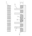
[0009]更に別の実行形態では、基板を処理するためのクラスタツールが提供される。クラスタツールは、ロードロックチャンバと、ロードロックチャンバの第1の側面に連結された移送チャンバと、移送チャンバに連結された複数の第1の処理チャンバであって、各々が流動性層の堆積を実施することができる堆積チャンバである、複数の第1の処理チャンバと、移送チャンバに連結された複数の第2の処理チャンバであって、各々が硬化処理を実施することができる硬化チャンバである、複数の第2の処理チャンバと、移送チャンバに連結された複数の第3の処理チャンバであって、各々がプラズマ硬化処理を実施することができるプラズマチャンバである、複数の第3の処理チャンバと、ロードチャンバの第2の側面に連結されたファクトリインターフェースとを含む。[0009] In yet another implementation, a cluster tool for processing a substrate is provided. The cluster tool includes a load lock chamber, a transfer chamber coupled to a first side of the load lock chamber, a plurality of first processing chambers coupled to the transfer chamber, each of the first processing chambers being a deposition chamber capable of performing a flowable layer deposition, a plurality of second processing chambers coupled to the transfer chamber, each of the second processing chambers being a curing chamber capable of performing a curing process, a plurality of third processing chambers coupled to the transfer chamber, each of the third processing chambers being a plasma chamber capable of performing a plasma curing process, and a factory interface coupled to a second side of the load chamber.
[0010]ある別の実行形態では、クラスタツールは、ロードロックチャンバと、ロードロックチャンバの第1の側面に連結された第1の真空移送チャンバと、第2の真空移送チャンバと、第1の真空移送チャンバと第2の真空移送チャンバとの間に配置された冷却ステーションと、ロードロックチャンバの第2の側面に連結されたファクトリインターフェースと、第1の真空移送チャンバに連結された複数の第1の処理チャンバであって、各々が流動性層の堆積を実施することができる堆積チャンバである、複数の第1の処理チャンバと、第2の真空移送チャンバに連結された複数の第2の処理チャンバであって、各々がプラズマ硬化処理を実施することができるプラズマチャンバである、複数の第2の処理チャンバとを含む。 [0010] In another implementation, a cluster tool includes a load-lock chamber, a first vacuum transfer chamber coupled to a first side of the load-lock chamber, a second vacuum transfer chamber, and a first vacuum transfer chamber. a cooling station disposed between the vacuum transfer chamber and the second vacuum transfer chamber; a factory interface coupled to the second side of the load lock chamber; and a plurality of vacuum transfer chambers coupled to the first vacuum transfer chamber. a plurality of first processing chambers, each of which is a deposition chamber capable of performing flowable layer deposition; and a plurality of second processing chambers coupled to a second vacuum transfer chamber. and a plurality of second processing chambers, each of which is a plasma chamber capable of performing a plasma curing process.
[0011]上述した本開示の特徴を詳細に理解できるように、一部が添付の図面に例示されている実行形態を参照しながら、上記に要約した本開示をより具体的に説明する。しかし、添付の図面は本開示の典型的な実行形態のみを示すものであり、したがって、実行形態の範囲を限定するものと見なすべきではなく、本開示は他の等しく有効な実行形態も許容しうることに留意されたい。[0011] In order that the above-mentioned features of the present disclosure may be understood in detail, the present disclosure summarized above will now be described more particularly with reference to embodiments, some of which are illustrated in the accompanying drawings. It should be noted, however, that the accompanying drawings depict only typical embodiments of the present disclosure and therefore should not be considered as limiting the scope of the embodiments, as the present disclosure may admit of other equally effective embodiments.
[0017]理解しやすくするために、可能な場合は図面に共通の同一要素を記号表示するのに同一の参照番号が使われている。具体的な記載がなくても、一実行形態で開示された要素を他の実行形態に有益に用いることは可能であると考えられる。 [0017] For ease of understanding, the same reference numerals have been used, where possible, to designate the same elements common to the drawings. It is contemplated that elements disclosed in one implementation may be beneficially used in other implementations, even without specific recitation.
[0018]図1は、トレンチの充填を促進する流動性誘電体層を形成する方法100における選択工程を示すフロー図である。図2Aに、基板200の一部の概略三次元図を示す。図2B~2Gは、図2AのラインA-Aに沿った半導体デバイス構造の一部の概略断面図である。図2B~2Gに、図1のフロー図による様々な製造段階中の図2Aの基板200を示す。説明をわかりやすくするために、図1及び図2A~2Gを合わせて説明する。 [0018] FIG. 1 is a flow diagram illustrating selected steps in a
[0019]方法100は、ブロック102において、図2Aに示す基板200等の基板を堆積チャンバの基板処理領域の中へ移送することによって開始される。適切な堆積チャンバには、高密度プラズマCVDチャンバ、プラズマ強化CVDチャンバ、低大気圧(sub-atmospheric:大気圧より低い圧力)CVDチャンバ等を含みうる。流動性酸化物/窒化物層を形成するように適合されうる例示の堆積チャンバは、いずれもカリフォルニア州サンタクララのアプライドマテリアルズ社から市販されているProducer(登録商標)ETERNA CVD(登録商標)システム又はUltima HDP CVD(登録商標)システムを含む。他のメーカーからの他の好適な堆積チャンバも用いることが可能だと考えられる。 [0019]
[0020]基板200は、上に形成されたフィン202を有する。各フィン202は、一又は複数のデバイスが形成される作用面積として機能しうる。フィン202は、マスキング、フォトリソグラフィ、及び/又はエッチング処理を含む、基板200上で行われる適切な処理を使用して基板200にトレンチ204を形成し、基板200から上向きに延びるフィン202を残すことで作製される。[0020]
[0021]トレンチ204のアスペクト比は、約1:1、約2:1、約3:1、約5:1、約10:1、約15:1、約20:1、約30:1、約50:1、約100:1以上であってよい。ある実行形態ではトレンチ204のアスペクト比は、約10:1~約30:1、例えば約15:1であってよい。本書に記載の「アスペクト比」という語は、特定の特徴、例えば基板200に形成されたトレンチ204の高さ寸法と幅寸法の比率を指すものである。 [0021] The aspect ratio of the
[0022]基板200は、シリコン(ドープされた又はドープされていない)、結晶シリコン(例:Si<100>又はSi<111>)、酸化ケイ素、ドープされた又はドープされていないポリシリコン等のシリコン基板、ゲルマニウム基板、シリコンゲルマニウム(SiGe)基板、ヒ化ガリウム基板等のIII-V複合基板、炭化ケイ素(SiC)基板、パターン化された又はパターン化されていない絶縁層上の半導体(SOI)基板、炭素がドープされた酸化物、窒化ケイ素、液晶ディスプレイ(LCD)、プラズマディスプレイ、エレクトロルミネセント(EL)ランプディスプレイ等のディスプレイ基板、ソーラアレー、ソーラーパネル、発光ダイオード(LED)基板、ガラス、サファイア、又は金属、金属合金及び他の導電性材料等の他のいずれかの材料等の、上に堆積された材料を有することができるいずれかの基板であってよい。一又は複数の電気デバイス、例えばトランジスタ、コンデンサ、抵抗器、ダイオード、フォトダイオード、ヒューズ等の様々なN型金属酸化膜半導体(NMOS)及び/又はP型金属酸化膜半導体(PMOS)デバイスを基板200に形成することができる。基板200は、任意の特定のサイズ又は形状に限定されないと考えられる。したがって、基板200は、中でも、200mmの直径、300mmの直径、又は450mm等の他の直径を有する円形基板であってよい。基板200はまた、任意の多角形、正方形、長方形、曲線状又は他の非円形ワークピースであってもよい。 [0022] The
[0023]ブロック104において、基板200の上に流動性層206が形成される。流動性層206は、少なくともシリコンを含有する誘電体層であってよい。ある実施形態では、流動性層206は、少なくともシリコン及び酸素を含有する誘電体層である。ある実施形態では、流動性層206は、少なくともシリコンと窒素を含有する誘電体層である。ある実施形態では、流動性層206は、少なくともシリコン、酸素及び窒素を含有する誘電体層である。流動性層206がシリコン、酸素及び窒素を含有する誘電体層である場合、基板200の上に流動性層206を形成するために、堆積チャンバの中へシリコン含有前駆体、酸素系ラジカル前駆体は、及び窒素系ラジカル前駆体が導入されうる。基板200の露出した表面に流動性層206が堆積され、トレンチ204が充填されうる。一実施形態では、図2Bに示すように、トレンチ204の底面207の上、及び側壁面209に沿って流動性層206が形成される。適切な流動性層206は、非限定的に、SiC、SiO、SiCN、SiO2、SiOC、SiOCN、SiON、又はSiNを含みうる。代替的に、流動性層206は、追跡可能な量の炭素を含まない(すなわち、炭素を含まない)場合がある。 [0023] In
[0024]流動性層206は、トレンチ204を継ぎ目なしに又はボイドなしにボトムアップで(底から)充填することを可能にする流動性を提供する。流動性は少なくとも一部において、堆積された層に存在する短鎖ポリシラザンポリマーに起因しうる。例えば、堆積された層は、シラザンタイプのSi-NH-Siバックボーン(すなわち、Si-N-H層)を有しうる。短鎖ポリマーの形成と流動性を可能にする窒素は、ラジカル前駆体又はシリコン含有前駆体のいずれかから由来のものである。誘電体層は流動性であるため、誘電体層によりトレンチ204にボイドをつくらずに高アスペクト比を有するトレンチをボトムアップで充填することができる。流動性層206の堆積は、規定の堆積厚さに達したときに停止されうる。一実施形態では、規定の堆積厚さ「T1」は、約20オングストローム~約300オングストロームの範囲である。誘電体層の流動性は、堆積が進むにつれ減少し、後続の硬化/プラズマ処理段階の間に実質的に除去される。 [0024]
[0025]適切なシリコン含有前駆体は、酸素原子とシリコン原子の比率が0~約6の有機ケイ素化合物を含みうる。適切な有機ケイ素化合物は、シロキサン化合物、テトラクロロシラン、ジクロロジエトキシシロキサン、クロロトリエトキシシロキサン、ヘキサクロロジシロキサン、及び/又はオクタクロロトリシロキサン等の一又は複数のハロゲン部分(例:フッ化物、塩化物、臭化物、又はヨウ化物)を含むハロゲン化されたシロキサン化合物、及びトリシリルアミン(TSA)、ヘキサメチルジシラザン(HMDS)、シラトラン、テトラキス(ジメチルアミノ)シラン、ビス(ジエチルアミノ)シラン、トリス(ジメチル-アミノ)クロロシラン、及びメチルシラトラン等のアミノシランであってよい。他のシリコン含有前駆体、例えばシラン、ハロゲン化されたシラン、オルガノシラン、及びそれらいずれかの組み合わせも使用可能である。シランは、シラン(SiH4)、及び実験式SixH(2x+2)を有する高次シラン、例えばジシラン(Si2H6)、トリシラン(Si3H8)、及びテトラシラン(Si4H10)、又は他の高次シラン、例えばポリクロロシランを含みうる。 [0025] Suitable silicon-containing precursors may include organosilicon compounds having a ratio of oxygen atoms to silicon atoms of 0 to about 6. Suitable organosilicon compounds include siloxane compounds, tetrachlorosilane, dichlorodiethoxysiloxane, chlorotriethoxysiloxane, hexachlorodisiloxane, and/or octachlorotrisiloxane containing one or more halogen moieties (e.g. fluoride, chloride). , bromide, or iodide); and trisilylamine (TSA), hexamethyldisilazane (HMDS), silatrane, tetrakis(dimethylamino)silane, bis(diethylamino)silane, tris(dimethyl -amino)chlorosilane, and methylsilatrane. Other silicon-containing precursors can also be used, such as silanes, halogenated silanes, organosilanes, and any combinations thereof. Silanes include silane (SiH4 ) and higher silanes with the empirical formula Six H(2x+2) , such as disilane (Si2 H6 ), trisilane (Si3 H8 ), and tetrasilane (Si4 H10 ), or other higher order silanes, such as polychlorosilanes.
[0026]酸素系ラジカル前駆体は、酸素(O2)、オゾン(O3)、NO、NO2、又はN2O等の窒素-酸素化合物、水又は過酸化物等の水素-酸素化合物、一酸化炭素又は二酸化炭素等の炭素-酸素化合物、及び他の酸素含有前駆体、及びそれらいずれかの組み合わせから形成された酸素ラジカルを含みうる。酸素ラジカルを、離れたところで生成し、シリコン含有前駆体と共に導入することが可能である。酸素系ラジカル前駆体は、堆積チャンバに導入する前に、例えばCCP(容量結合プラズマ)又はICP(誘導結合プラズマ)構成を有しうる遠隔プラズマ源を使用して活性化させることができる。 [0026] The oxygen-based radical precursor is a nitrogen-oxygen compound such as oxygen (O2 ), ozone (O3 ), NO, NO2 or N2 O, a hydrogen-oxygen compound such as water or peroxide, It can include oxygen radicals formed from carbon-oxygen compounds such as carbon monoxide or carbon dioxide, and other oxygen-containing precursors, and any combination thereof. Oxygen radicals can be generated remotely and introduced together with silicon-containing precursors. The oxygen-based radical precursors can be activated using a remote plasma source, which can have, for example, a CCP (capacitively coupled plasma) or ICP (inductively coupled plasma) configuration before being introduced into the deposition chamber.
[0027]窒素系ラジカル前駆体は、窒素(N2)、亜酸化窒素(N2O)、一酸化窒素(NO)、二酸化窒素(NO2)、アンモニア(NH3)、及びそれらいずれかの組み合わせから形成される窒素ラジカルを含みうる。窒素ラジカルを離れたところで生成し、シリコン含有前駆体及び酸素系ラジカル前駆体と共に導入することができる。窒素系ラジカル前駆体は、堆積チャンバに導入する前に、例えばCCP(容量結合プラズマ)又はICP(誘導結合プラズマ)構成を有しうる遠隔プラズマ源を使用して活性化させることができる。 [0027] Nitrogen-based radical precursors may include nitrogen radicals formed from nitrogen (N2 ), nitrous oxide (N2O ), nitric oxide (NO), nitrogen dioxide (NO2 ), ammonia (NH3 ), and any combination thereof. Nitrogen radicals may be generated remotely and introduced along with the silicon-containing precursor and the oxygen-based radical precursor. The nitrogen-based radical precursor may be activated using a remote plasma source, which may have, for example, a CCP (capacitively coupled plasma) or ICP (inductively coupled plasma) configuration, prior to introduction into the deposition chamber.
[0028]ある実行形態では、酸素系ラジカル前駆体が第1の体積流量で堆積チャンバの中へ流入され、シリコン含有前駆体が第2の体積流量で堆積チャンバの中へ流入され、第1の体積流量と第2の体積流量の比率は、約0.3:1と約0.9:1、例えば約0.5:1と約0.7:1との間、例えば約0.6:1に制御されうる。 [0028] In some implementations, the oxygen-based radical precursor is flowed into the deposition chamber at a first volumetric flow rate, the silicon-containing precursor is flowed into the deposition chamber at a second volumetric flow rate, and the silicon-containing precursor is flowed into the deposition chamber at a second volumetric flow rate; The ratio of the volumetric flow rate to the second volumetric flow rate is between about 0.3:1 and about 0.9:1, such as between about 0.5:1 and about 0.7:1, such as about 0.6:1. 1.
[0029]ある実行形態では、窒素系ラジカル前駆体が第1の体積流量で堆積チャンバの中へ流入され、シリコン含有前駆体が第2の体積流量で堆積チャンバの中へ流入され、第1の体積流量と第2の体積流量の比率は、約0.2:1と約0.8:1、例えば約0.4:1と約0.6:1との間、例えば約0.5:1に制御されうる。 [0029] In some implementations, a nitrogen-based radical precursor is flowed into the deposition chamber at a first volumetric flow rate, a silicon-containing precursor is flowed into the deposition chamber at a second volumetric flow rate, and the silicon-containing precursor is flowed into the deposition chamber at a second volumetric flow rate; The ratio of the volumetric flow rate to the second volumetric flow rate is between about 0.2:1 and about 0.8:1, such as between about 0.4:1 and about 0.6:1, such as about 0.5:1. 1.
[0030]酸素及び窒素ラジカルの両方を含有するラジカル前駆体が使用される場合は、酸素系ラジカル前駆体、又は窒素系ラジカル前駆体を省くことができると考えられる。 [0030] If a radical precursor containing both oxygen and nitrogen radicals is used, it is contemplated that the oxygen-based radical precursor or the nitrogen-based radical precursor may be omitted.
[0031]シリコン含有前駆体、酸素系ラジカル前駆体、及び窒素系ラジカル前駆体は、摂氏約150以下、例えば摂氏約100度以下、例えば摂氏約65度の温度で反応しうる。流動性誘電体層の形成中、堆積チャンバのチャンバ圧力は、約0.1トール~約10トール、例えば約0.5トール~約6トールに維持されうる。十分に薄い堆積を制御するために、堆積速度は約50オングストローム/秒以下に制御されうる。ある実行形態では、堆積速度は、約5オングストローム/秒以下、例えば約4オングストローム/秒に制御される。堆積速度が遅い(5Å/秒以下)ことで、ある用途においては、ボイドがなく、表面粗さの滑らかな流動性層の形成が可能になるため有利になりうる。[0031] The silicon-containing precursor, the oxygen-based radical precursor, and the nitrogen-based radical precursor may react at a temperature of about 150 degrees Celsius or less, such as about 100 degrees Celsius or less, such as about 65 degrees Celsius. During the formation of the flowable dielectric layer, the chamber pressure of the deposition chamber may be maintained at about 0.1 Torr to about 10 Torr, such as about 0.5 Torr to about 6 Torr. To control a sufficiently thin deposition, the deposition rate may be controlled to about 50 Angstroms/second or less. In some implementations, the deposition rate is controlled to about 5 Angstroms/second or less, such as about 4 Angstroms/second. A slow deposition rate (5 Å/second or less) may be advantageous in some applications by allowing the formation of a flowable layer without voids and with smooth surface roughness.
[0032]ブロック106において、流動性層が規定の堆積厚さ「T1」(例:約20~300Å)に達したら、シリコン含有前駆体、酸素系ラジカル前駆体、及び窒素系ラジカル前駆体の流れが停止され、図2Cに示すように、硬化チャンバにおいて基板に第1の硬化処理231が行われる。硬化後の流動性層206は高い密度、良好な安定性を呈し、後続のプラズマ処理(ブロック108)において実施される高温に耐えることができる。硬化チャンバは、UV光硬化、熱硬化、マイクロ波硬化、プラズマ硬化、電子ビーム硬化、又は中性(粒子)ビーム硬化等のいずれかの好適な硬化技法を使用しうる。ある実行形態では、硬化処理はオプションであり、省略することが可能である。ある実行形態では、硬化チャンバはUV硬化チャンバである。例示の硬化チャンバは、いずれもカリフォルニア州サンタクララのアプライドマテリアルズ社から市販されているProducer(登録商標)NANOCURETM3 UV硬化チャンバを含みうる。他のメーカーからの他の好適な硬化チャンバを用いて本書に記載の処理を実施することも可能であると考えられる。 [0032] At
[0033]硬化処理231は、酸素含有雰囲気、窒素含有雰囲気、及び/又は不活性ガス雰囲気下で実施されうる。酸素含有雰囲気は、分子状酸素(O2)、オゾン(O3)、水蒸気(H2O)、一酸化窒素(NO)、二酸化窒素(NO2)、亜酸化窒素(N2O)、及びそれらいずれかの組み合わせ等の一又は複数の酸素含有ガスを硬化チャンバの中へ導入することによって作られうる。窒素含有雰囲気は、窒素(N2)、アンモニア(NH3)、及びそれらいずれかの組み合わせ等の一又は複数の窒素含有ガスを硬化チャンバの中へ導入することによって作られうる。不活性雰囲気は、ヘリウム、アルゴン、水素、クリプトン、キセノン、及びそれらいずれかの組み合わせを硬化チャンバの中へ導入することによって作られうる。必要に応じ、酸素/窒素原子を流動性層206の中に組み込みやすくするために、ラジカル系雰囲気下で、すなわち、酸素含有ガス、窒素含有ガス、又は不活性ガスからのラジカルを使用して硬化処理を実施することが可能である。 [0033] The
[0034]流動性層が酸化物である幾つかの実施形態では、硬化処理231は、酸素含有雰囲気下で実施されうる。上記の場合、硬化処理は、酸素挿入及び膜架橋の目的でオゾン雰囲気下で熱又はUVを使用しうる。酸素含有雰囲気は、シリコン含有層でありうる流動性層を酸化ケイ素層に変換させる酸素を提供する。流動性層が窒化物である場合、硬化処理は、窒素含有雰囲気下で実施されうる。上記の場合、硬化処理は、窒素又はアンモニア雰囲気下でUVを使用して流動性層を窒化させ、堆積された層の窒素濃度を増加させうる。いずれの場合でも、硬化処理は、堆積された層の揮発性結合を安定化させ、これにより、プラズマ処理(ブロック108)前に熱的に安定した層を形成する助けとなりうる。通常、長いUV処理の結果、プラズマ処理後の収縮が低減し、膜応力が中立に近くなる。 [0034] In some embodiments where the flowable layer is an oxide, the
[0035]一実行形態では、硬化処理231は、UV光硬化技法を使用する。硬化処理により、所望の(反応的又は不活性)雰囲気、温度及び圧力下で熱的に又はUV光子の助けで膜架橋を可能にすることができる。例示のUV光硬化技法は、基板上に光を投射する一又は複数のUV光源から光又は光子エネルギーを供給することを含みうる。これらのUV光源には、UV波長(例:220nm)にピーク強度を有する広い波長スペクトル(UV波長以外を含む)にわたって光を放出するUVランプが含まれうる。UVランプの例には、他の種類のUVランプの中でも、キセノンランプ(ピーク発光波長:172nm)、水銀ランプ(ピーク:243nm)、重水素ランプ(ピーク:140nm)、塩化クリプトン(KrCl2)ランプ(ピーク:222nm)が含まれる。更なるUV光源には、流動性層にコヒーレントな狭帯域のUV光を提供するレーザが含まれうる。レーザ光源には、エキシマレーザ(例:XeCl、KrF、F2等、エキシマレーザ)及び/又は固体レーザ(例:Nd-YAGレーザ)の適切な高調波が含まれうる。UV光源は、ダイオードUV光源も含みうる。 [0035] In one implementation, curing
[0036]硬化処理231の間に、流動性層206は約10秒~約60分の間硬化され、これは用途によって変わりうる。硬化チャンバの圧力は、約1トールから約600トールまでの範囲、例えば約10トール~150トールであってよい。硬化温度は、摂氏約5度から摂氏約1100度の範囲、例えば摂氏約10度、摂氏約25度、摂氏約50度、摂氏約100度、摂氏約200度、摂氏約300度、摂氏約400度、摂氏約500度、摂氏約600度、摂氏約700度、摂氏約800度、摂氏約900度、摂氏約1000度であってよい。一例において、硬化処理は、約100秒の間、摂氏約350度の温度及び約500トールのオゾン雰囲気下で実施される熱硬化処理である。 [0036] During the
[0037]熱硬化が適合される幾つかの場合では、硬化処理は、硬化温度及び圧力に依存して、流動性層206が堆積される堆積チャンバにおいてインシトゥで実施されうる、又はプラズマ処理が実施されるプラズマチャンバ(ブロック108)において実施されうる。 [0037] In some cases where thermal curing is adapted, the curing process may be performed in situ in the deposition chamber where the
[0038]ブロック108において、堆積処理が完了した後(又は実施される場合はオプションの硬化処理後)に、図2Dに示すように、基板200上に形成された誘電体層を更に硬化させるために、プラズマチャンバにおいて基板200に第2の硬化処理233が行われる。一実施形態では、第2の硬化処理233は、プラズマ処理である。プラズマチャンバは、プラズマ又はプラズマ支援技術を使用するいずれかの好適なチャンバであってよい。プラズマチャンバは、高温において高密度プラズマを発生させ、高密度プラズマからのイオンを衝突させて、硬化処理する層(ブロック106)又は流動性誘電体層(ブロック104、硬化処理が実施されない場合)を高密度化し更に硬化させる。 [0038] At
[0039]材料によっては、プラズマ処理は、酸素含有雰囲気(硬化処理する層又は流動性誘電体層が酸化物である場合)、又は窒素含有雰囲気(硬化処理する層又は流動性誘電体層が窒化物である場合)下で実施されうる。酸素含有雰囲気は、分子状酸素(O2)、オゾン(O3)、水蒸気(H2O)、一酸化窒素(NO)、二酸化窒素(NO2)、亜酸化窒素(N2O)、及びそれらいずれかの組み合わせ等の一又は複数の酸素含有ガスをプラズマチャンバの中へ導入することによって作られうる。窒素含有雰囲気は、窒素(N2)、アンモニア(NH3)、及びそれらいずれかの組み合わせ等の一又は複数の窒素含有ガスをプラズマチャンバの中へ導入することによって作られうる。いずれの場合にも、プラズマチャンバの中へアルゴン、水素、又はヘリウム等の不活性ガスが導入されうる。例えば、硬化処理する層又は流動性誘電体層が酸化物である場合、プラズマ処理は、酸素/ヘリウム雰囲気、酸素/アルゴン雰囲気、又は酸素/水素雰囲気下で実施されうる。硬化処理する層又は流動性誘電体層が窒化物である場合、プラズマ処理は、窒素/アンモニア雰囲気、窒素/水素雰囲気、又は窒素/ヘリウム雰囲気下で実施されうる。 [0039] Depending on the material, plasma treatment may be performed in an oxygen-containing atmosphere (if the hardening layer or flowable dielectric layer is an oxide) or in a nitrogen-containing atmosphere (if the hardening layer or flowable dielectric layer is a nitride). (if it is a product) The oxygen-containing atmosphere includes molecular oxygen (O2 ), ozone (O3 ), water vapor (H2 O), nitric oxide (NO), nitrogen dioxide (NO2 ), nitrous oxide (N2 O), and It may be created by introducing one or more oxygen-containing gases, such as any combination thereof, into the plasma chamber. A nitrogen-containing atmosphere may be created by introducing one or more nitrogen-containing gases into the plasma chamber, such as nitrogen (N2 ), ammonia (NH3 ), and any combination thereof. In either case, an inert gas such as argon, hydrogen, or helium may be introduced into the plasma chamber. For example, if the layer to be cured or the flowable dielectric layer is an oxide, the plasma treatment may be performed under an oxygen/helium atmosphere, an oxygen/argon atmosphere, or an oxygen/hydrogen atmosphere. When the layer to be hardened or the flowable dielectric layer is a nitride, the plasma treatment can be performed under a nitrogen/ammonia atmosphere, a nitrogen/hydrogen atmosphere, or a nitrogen/helium atmosphere.
[0040]ある実行形態では、プラズマ処理はラジカル系処理であってよい。例えば、酸素含有雰囲気は、離れたところで生成され、プラズマチャンバの中に搬送されうるラジカル酸素核種及び/又はラジカルヒドロキシル種であってよい、又は更にそれらを含みうる。同様に、窒素含有雰囲気は、離れたところで生成され、プラズマチャンバの中に搬送されうるラジカル窒素核種であってよい、又は更にそれらを含みうる。ラジカルを使用するプラズマ処理は、高圧力(例:1トール以上、例えば約10~40トール)下で、及び/又はパルスRF電力波形を用いて実施されうる。例えば、プラズマ処理は、標準モード(すなわち、同じRF周波数を使用し、コイルアンテナを通って流れる電流が同位相である)で動作するパルスソース電力を使用する誘導結合プラズマであってよい。 [0040] In some implementations, the plasma treatment may be a radical-based treatment. For example, the oxygen-containing atmosphere can be or even include radical oxygen species and/or radical hydroxyl species that can be generated remotely and transported into the plasma chamber. Similarly, the nitrogen-containing atmosphere may be or even include radical nitrogen species that may be generated remotely and transported into the plasma chamber. Plasma processing using radicals can be performed under high pressure (eg, 1 Torr or more, eg, about 10-40 Torr) and/or using pulsed RF power waveforms. For example, the plasma treatment may be an inductively coupled plasma using pulsed source power operated in standard mode (ie, using the same RF frequency and the currents flowing through the coil antenna are in phase).
[0041]プラズマ処理の間、硬化処理する層又は流動性誘電体層は更に、プラズマチャンバにおいて存在する酸素又は窒素雰囲気に起因して、酸化物又は窒化物に変換される。Si-N結合エネルギー(355KJ/mol)とN-H結合エネルギー(386KJ/mol)はSi-O結合エネルギー(452KJ/mol)よりも低いために、酸素雰囲気により、硬化処理する層又は流動性誘電体層のSi-N結合又はN-H結合のSi-O結合への置換が促される。したがって、プラズマ処理が酸素含有雰囲気下で実施される場合、硬化処理する層又は流動性誘電体層(Si-NH-Siバックボーンを有する)は更に、酸化ケイ素層に変換される。プラズマ処理が窒素含有雰囲気下で実施される場合、硬化処理する層又は流動性誘電体層(Si-NH-Siバックボーンを有する)は更に、窒化ケイ素層に変換される。したがって、プラズマ処理は、1つの工程に物質の変換と高密度化を組み合わせたものであり、従来、FCVD膜を形成する硬化処理後に層の中に更に酸素又は窒素原子を組み込むために通常実施される長時間の熱アニール処理は必要ない。また、高密度プラズマにより、熱アニールに比べて低いサーマルバジェットも可能になりうる。この結果、製造処理の全体的なサーマルバジェットが削減される。 [0041] During plasma processing, the hardening layer or flowable dielectric layer is further converted to an oxide or nitride due to the oxygen or nitrogen atmosphere present in the plasma chamber. Since the Si-N bond energy (355 KJ/mol) and N-H bond energy (386 KJ/mol) are lower than the Si-O bond energy (452 KJ/mol), the layer to be hardened or the fluid dielectric This promotes the substitution of Si--N bonds or N--H bonds in the body layer with Si--O bonds. Thus, if the plasma treatment is carried out under an oxygen-containing atmosphere, the hardening layer or flowable dielectric layer (with a Si--NH--Si backbone) is further converted into a silicon oxide layer. If the plasma treatment is carried out under a nitrogen-containing atmosphere, the hardening layer or flowable dielectric layer (with a Si--NH--Si backbone) is further converted into a silicon nitride layer. Plasma treatment therefore combines material transformation and densification in one step and is conventionally typically performed to incorporate further oxygen or nitrogen atoms into the layer after the curing process to form an FCVD film. No long-term thermal annealing is required. High-density plasmas may also allow for lower thermal budgets compared to thermal anneals. This results in a reduction in the overall thermal budget of the manufacturing process.
[0042]ある実行形態では、プラズマ処理は、酸素/ヘリウム雰囲気、酸素/アルゴン雰囲気、又は酸素/水素雰囲気(硬化処理する層又は流動性誘電体層が酸化物である場合)を使用する第1のプラズマ処理工程と、ヘリウム等の不活性ガス雰囲気を使用する第2のプラズマ処理工程を含む2つの工程処理である。硬化処理する層又は流動性誘電体層が窒化物である場合、プラズマ処理は、窒素/アンモニア雰囲気、窒素/水素雰囲気、又は窒素/ヘリウム雰囲気を使用する第1のプラズマ処理工程と、ヘリウム等の不活性環境を使用する第2のプラズマ処理工程とを含みうる。不活性環境(例:ヘリウム)下でのプラズマ処理は、高エネルギーイオンによる衝突により膜の既存の結合が外れて再構成が起き、膜応力が解放され、密度の高い網状組織が形成されうるため、膜の高密度化に効果的である。 [0042] In some implementations, the plasma treatment comprises a first step using an oxygen/helium atmosphere, an oxygen/argon atmosphere, or an oxygen/hydrogen atmosphere (if the hardening layer or flowable dielectric layer is an oxide). It is a two step process including a plasma processing step and a second plasma processing step using an inert gas atmosphere such as helium. If the layer to be hardened or the flowable dielectric layer is a nitride, the plasma treatment may include a first plasma treatment step using a nitrogen/ammonia atmosphere, a nitrogen/hydrogen atmosphere, or a nitrogen/helium atmosphere, and a nitrogen/helium atmosphere such as helium. and a second plasma treatment step using an inert environment. Plasma treatment in an inert environment (e.g., helium) can cause reorganization by breaking existing bonds in the membrane due to bombardment by high-energy ions, releasing membrane stress and forming a dense network. , is effective in increasing the density of the film.
[0043]プラズマチャンバは、プラズマ源発生装置への電源入力及び基板バイアス装置への電源入力に対して別々の制御を有するいずれかの好適なプラズマリアクタであってよい。一実行形態では、プラズマチャンバは、誘導結合プラズマ(ICP)チャンバである。上記の場合、プラズマチャンバは、プラズマ密度(ソース電力)を決定する誘導結合RF電力の供給を制御するプラズマ源コントローラと、基板表面にバイアス電圧(バイアス電力)を発生させるために使用されるRF電力又はDC電力の供給を制御するバイアスコントローラとを有しうる。このバイアス電圧は、処理領域で形成されたプラズマからのイオンを基板200に引き付けるために使用される。このバイアス電圧を使用して、硬化処理する層(又は、硬化処理が実施されない場合は流動性誘電体層)へのイオン核種の衝突エネルギーを制御することができる。ソース電力及び圧力は、イオン化を制御する調整つまみ(knob)である。バイアス電力は、膜処理の深さ制御においてイオンエネルギーを調整するための追加の調整つまみを提供する。バイアス電力に加えて、低い圧力(例:約5ミリトール未満)により、長い平均自由路と、深いトレンチ層の処理が可能になる。ある好適なプラズマチャンバは、カリフォルニア州サンタクララのアプライドマテリアルズ社から市販されているCentura(登録商標)AdvantedgeTM MesaTMエッチングチャンバである。 [0043] The plasma chamber may be any suitable plasma reactor with separate controls for the power input to the plasma source generator and the power input to the substrate bias device. In one implementation, the plasma chamber is an inductively coupled plasma (ICP) chamber. In the above case, the plasma chamber includes a plasma source controller that controls the delivery of inductively coupled RF power that determines the plasma density (source power) and RF power that is used to generate a bias voltage (bias power) at the substrate surface. Alternatively, it may have a bias controller that controls the supply of DC power. This bias voltage is used to attract ions from the plasma formed in the processing region to the
[0044]本開示においてプラズマを形成するための一例としてICPチャンバが使用されているが、容量結合プラズマ(CCP)源、分離されたプラズマ源(DPS)、マグネトロンプラズマ源、電子サイクロトロン共鳴(ECR)源、又はマイクロ波プラズマ源等の他のプラズマ源も使用可能であると考えられる。[0044] Although an ICP chamber is used as an example for forming the plasma in this disclosure, it is contemplated that other plasma sources, such as a capacitively coupled plasma (CCP) source, a decoupled plasma source (DPS), a magnetron plasma source, an electron cyclotron resonance (ECR) source, or a microwave plasma source, may also be used.
[0045]ICPチャンバが使用される場合、プラズマ処理を実施するために以下のチャンバ処理パラメータが使用されうる。これらのパラメータは、上述したように、硬化処理する層(ブロック106)又は流動性誘電体層(ブロック104)を処理するために使用されうる。様々な実行形態では、硬化処理する層は、酸化物又は窒化物である。チャンバの圧力は、約1ミリトール(mTorr)~約10トール、例えば約2ミリトール~約1トール、例えば約5ミリトール~約88ミリトールであってよい。ソース電力は、約50ワット(W)~約650W、例えば約100W~約500W、例えば約250W~約450Wであってよい。ソース電力は、約30MHz~約60MHzの高周波(RF)帯域で印加されうる。ICPチャンバの基板支持体に供給されるバイアス電力は、約10W~約450W、例えば約50W~約300W、例えば100W~約200Wであってよい。バイアス電力は、約10MHz~約30MHzの高周波(RF)帯域で印加されうる。基板温度は、摂氏約550度以下、例えば摂氏約300度~摂氏約500度、例えば摂氏約350度であってよい。第1のガス(例:酸素含有ガス又は窒素含有ガス)のガス流は、約60sccm~約5000sccm、例えば約100sccm~約2200sccm、例えば約300sccm~約1000sccmであってよい。第2のガス(例:不活性ガス)のガス流は、約5sccm~約250sccm、例えば約10sccm~約150sccm、例えば約20sccm~約100sccmであってよい。処理時間は、約10秒~約120秒、例えば約30秒~約90秒、例えば約45秒~約60秒であってよい。本書に記載の処理パラメータは、300mm基板に基づくものである。これらの処理パラメータは、硬化処理する層(ブロック106)又は流動性誘電体層(ブロック104)の厚さ、トレンチ204のサイズ、基板200のサイズ、プラズマチャンバの性能、及び用途等によって変化しうると考えられる。 [0045] If an ICP chamber is used, the following chamber processing parameters may be used to perform the plasma processing. These parameters may be used to process the layer to be cured (block 106) or the flowable dielectric layer (block 104), as described above. In various implementations, the hardened layer is an oxide or a nitride. The pressure in the chamber may be from about 1 mTorr to about 10 Torr, such as from about 2 mTorr to about 1 Torr, such as from about 5 mTorr to about 88 mTorr. The source power may be about 50 watts (W) to about 650W, such as about 100W to about 500W, such as about 250W to about 450W. Source power may be applied in a radio frequency (RF) band of about 30 MHz to about 60 MHz. The bias power supplied to the substrate support of the ICP chamber may be about 10W to about 450W, such as about 50W to about 300W, such as 100W to about 200W. Bias power may be applied in a radio frequency (RF) band from about 10 MHz to about 30 MHz. The substrate temperature may be less than or equal to about 550 degrees Celsius, such as from about 300 degrees Celsius to about 500 degrees Celsius, such as about 350 degrees Celsius. The gas flow of the first gas (eg, oxygen-containing gas or nitrogen-containing gas) may be from about 60 sccm to about 5000 sccm, such as from about 100 sccm to about 2200 sccm, such as from about 300 sccm to about 1000 sccm. The gas flow of the second gas (eg, inert gas) may be from about 5 sccm to about 250 sccm, such as from about 10 sccm to about 150 sccm, such as from about 20 sccm to about 100 sccm. Processing times may be about 10 seconds to about 120 seconds, such as about 30 seconds to about 90 seconds, such as about 45 seconds to about 60 seconds. The processing parameters described herein are based on a 300mm substrate. These processing parameters may vary depending on the thickness of the layer being cured (block 106) or the flowable dielectric layer (block 104), the size of the
[0046]ブロック108の後に、図2Eに示すように、堆積された誘電体層(すなわち、硬化及び/又は処理された流動性層206)が目標の高さ「T2」に達したか否かの決定110がなされる。堆積された誘電体層の目標の高さ「T2」は、トレンチ204の底面207から堆積された誘電体層の上面211までを測って約500オングストローム~約8000オングストローム、例えば約1000オングストローム~約6000オングストロームであってよい。目標の高さ「T2」に達していない場合、硬化/プラズマ処理された層の厚さを再び目的の厚さと比較する前に、堆積/硬化/プラズマ処理(例:ブロック104~108)のサイクルがもう一度実施されうる。堆積された誘電体層がターゲットの高さ「T2」に達するまで、ブロック104、106、及び108の処理が繰り返されうる。 [0046] After
[0047]目標の高さ「T2」に達したら、図2Cに示すように、堆積された誘電体層は、化学機械平坦化法(CMP)等によって平坦化されて、フィン202の上面208と堆積された誘電体層の上面210は、同一平面となる。次に、許容可能なエッチング処理等を使用することにより基板200に凹部が形成され、フィン202の上部213が現れうる又は露出しうる。プラズマ処理(ブロック108)が行われる同じプラズマチャンバにおいてエッチング処理が実施されうる。その後基板200は、プラズマチャンバからロードロックチャンバへ、そして次に一又は複数の前方開口型統一ポッド(FOUP)へ移送され、前方開口型統一ポッド(FOUP)において、集積回路チップを製造するのに要しうる置換ゲートの形成、エピタキシャル堆積、洗浄、アニーリング、熱、化学気相堆積、酸化又は窒化処理等の下流処理のために、他の処理システムへ移送される。 [0047] Once the target height "T2" is reached, the deposited dielectric layer is planarized, such as by chemical mechanical planarization (CMP), to form the
[0048]図3は、本開示の実行形態に係る、図1に記載の処理シーケンスを実施するために使用されうる処理システム300の概略上面図である。処理システム300の一例は、カリフォルニア州サンタクララのアプライドマテリアルズ社から市販されているPRODUCER(登録商標)又はCENTRISTMシステムである。処理システム300は、真空気密処理プラットフォーム302と、ファクトリインターフェース304とを含む。プラットフォーム202は、真空基板移送チャンバ312に連結された複数の処理チャンバ306a~b、308a~b、310a~bと、真空基板移送チャンバ312とファクトリインターフェース304との間に配置され、それらに連結されたロードロックチャンバ314とを含む。 [0048] Figure 3 is a schematic top view of a
[0049]ファクトリインターフェース304は、基板の移送を容易にする少なくとも1つのファクトリインターフェースロボット316、318を含む。ファクトリインターフェース304は、一又は複数の前方開口型統一ポッド(FOUP)320を受け入れるように構成される。一例では、3つのFOUPが適合されている。ファクトリインターフェースロボット316、318は、ファクトリインターフェース304から処理プラットフォーム302へ基板(例:ブロック102に記載の基板)を移送し、処理プラットフォーム302において少なくとも1つの移送ロボット322がファクトリインターフェースロボット316、318から基板を受け取って、次に、処理チャンバ306a~b、308a~b、310a~bのいずれかへそれらを移送する。一実行形態では、処理チャンバ306a~bは、ブロック104に記載の処理を実施するために使用されうる堆積チャンバである。処理チャンバ308a~bは、ブロック106に記載の処理を実施するために使用されうる硬化チャンバである。処理チャンバ310a~bは、ブロック108に記載の処理及びフィンを露出させる処理を実施するために使用されうるプラズマチャンバである。処理が完了すると、基板は移送ロボット322によってロードロックチャンバ314へ移送される。次に、ファクトリインターフェースロボット314、316はロードロックチャンバ314から基板を受け取って、それらを再びFOUP320へ搬送する。 [0049]
[0050]図4は、本開示の実行形態に係る、図1に示す処理シーケンスの処理を実施するために使用されうる処理システム400の概略上面図である。ある例示の実行形態では、処理システム400は、図1に示す特定の処理(例:ブロック102、104及び108)を実施するために使用されるハイボリューム製造(HVM)システムである。処理システム400は、真空気密処理プラットフォーム402と、ファクトリインターフェース404とを含む。プラットフォーム402は、それぞれ第1の真空基板移送チャンバ412と第2の真空基板移送チャンバ413とに連結された複数の処理チャンバ406a~d、408a~fと、第1の真空基板移送チャンバ412と第2の真空基板移送チャンバ413との間に配置された冷却ステーション415と、第1の真空基板移送チャンバ412とファクトリインターフェース404との間に配置され、それらに連結されたロードロックチャンバ414とを含む。 [0050] FIG. 4 is a schematic top view of a
[0051]ファクトリインターフェース404は、基板の移送を容易にする少なくとも1つのファクトリインターフェースロボット416、418を含む。ファクトリインターフェース404は、一又は複数の前方開口型統一ポッド(FOUP)420を受け入れるように構成される。一例では、4つのFOUPが適合されている。ファクトリインターフェースロボット416、418は、ファクトリインターフェース404から処理プラットフォーム402へ基板(例:ブロック102に記載の基板)を移送する。第1の真空基板移送チャンバ412の少なくとも1つの移送ロボット422は、ファクトリインターフェースロボット416、418から基板を受け取り、次に処理チャンバ406a~dのいずれかへそれらを移送する。一実行形態では、処理チャンバ406a~dはブロック108に記載の処理を実施するために使用されうるプラズマチャンバである。第1の真空基板移送チャンバ412と第2の真空基板移送チャンバ413との間で基板を移送するために、冷却ステーション415にオプションの移送ロボット417が配置されうる。第2の真空基板移送チャンバ413の少なくとも1つの移送ロボット419は冷却ステーション415から基板を受け取り、次に、処理チャンバ408a~fのいずれかへそれらを移送する。代替的に、移送ロボット417を省略することができ、移送ロボット417、422を協働させて、第1の真空基板移送チャンバ412と第2の真空基板移送チャンバ413との間で基板を移送することができる。一実行形態では、処理チャンバ408a~fは、ブロック104に記載の処理を実施するために使用されうる堆積チャンバである。堆積された誘電体層が目標の高さに達するまで、堆積チャンバ(すなわち、処理チャンバ408a~f)とプラズマチャンバ(すなわち、処理チャンバ406a~d)との間で基板が移送されうる。処理が完了すると、基板はロードロックチャンバ414へ移送される。次にファクトリインターフェースロボット414、416がロードロックチャンバ414から基板を受け取って、FOUP420へそれらを再び搬送する。 [0051]
[0052]概括すれば、本書に記載の実行形態は、流動性誘電体層を用いて基板にトレンチを形成し、充填するための方法に関するものである。本方法は、誘電体層をターゲット層の組成に変換し、高密度化するために、酸素含有/不活性ガス又は窒素含有/不活性ガス雰囲気下で高密度の誘導結合プラズマからのイオンを流動性誘電体層に衝突させることを含む。膜架橋と、酸素/窒素原子の流動性誘電体層への組み込みを助けるために、流動性堆積とプラズマ処理との間に硬化処理を挿入してもよい。これらの処理は、所望の厚さに達するまでサイクルとして実施される。サイクル処理により、トレンチの側壁への堆積を最小限に抑えながら、トレンチ底部の誘電体層の安定した良好な品質が可能になる。 [0052] Generally speaking, implementations described herein relate to a method for forming and filling trenches in a substrate using a flowable dielectric layer. The method involves flowing ions from a dense inductively coupled plasma in an oxygen-containing/inert gas or nitrogen-containing/inert gas atmosphere to transform and densify the dielectric layer to the composition of the target layer. impingement on a dielectric layer. A curing process may be inserted between flowable deposition and plasma treatment to aid in film cross-linking and incorporation of oxygen/nitrogen atoms into the flowable dielectric layer. These treatments are performed in cycles until the desired thickness is reached. The cycling process allows for consistently good quality of the dielectric layer at the bottom of the trench while minimizing deposition on the sidewalls of the trench.
[0053]以上の記述は本開示の実行形態を対象としているが、本開示の基本的な範囲から逸脱することなく本開示の他の実行形態及び更なる実行形態が考案されてよく、本開示の範囲は、下記の特許請求の範囲によって決定される。 [0053] Although the above description is directed to implementations of this disclosure, other implementations and further implementations of this disclosure may be devised without departing from the essential scope of this disclosure, and The scope of is determined by the claims below.
Claims (18)
Translated fromJapaneseロードロックチャンバと、
前記ロードロックチャンバの第1の側面に連結された移送チャンバと、
前記移送チャンバに連結された複数の第1の処理チャンバであって、前記第1の処理チャンバの各々が流動性層の堆積を実施することができる堆積チャンバであり、前記第1の処理チャンバの少なくとも1つがシリコン含有誘電体層を堆積するように構成されている、複数の第1の処理チャンバと、
前記移送チャンバに連結された複数の第2の処理チャンバであって、前記第2の処理チャンバの各々が硬化処理を実施することができる硬化チャンバであり、前記第2の処理チャンバの少なくとも1つがUV光硬化チャンバであり、前記第2の処理チャンバの前記少なくとも1つは、酸素、窒素、又は不活性ガスを含むラジカル系雰囲気下で硬化処理を実施するように構成されている、複数の第2の処理チャンバと、
前記移送チャンバに連結された複数の第3の処理チャンバであって、前記第3の処理チャンバの各々がプラズマ硬化処理を実施することができるプラズマチャンバであり、前記第3の処理チャンバの少なくとも1つが誘導結合プラズマ(ICP)チャンバである、複数の第3の処理チャンバと、
前記ロードロックチャンバの第2の側面に連結されたファクトリインターフェースと、
前記基板を、前記第1の処理チャンバの前記少なくとも1つ、前記第2の処理チャンバの前記少なくとも1つ、前記第3の処理チャンバの前記少なくとも1つにこの順序で移送して処理するように構成された制御部と、
を備え、
前記複数の第1の処理チャンバは、前記複数の第2の処理チャンバ及び前記複数の第3の処理チャンバに隣接し、
前記ロードロックチャンバは、前記複数の第2の処理チャンバ及び前記複数の第3の処理チャンバに隣接する、
クラスタツール。 1. A cluster tool for processing a substrate, comprising:
A load lock chamber;
a transfer chamber coupled to a first side of the load lock chamber;
a plurality of first processing chambers coupled to the transfer chamber, each of the first processing chambers being a deposition chamber capable of performing a flowable layer deposition, at least one of the first processing chambers being configured to deposit a silicon-containing dielectric layer;
a plurality of second processing chambers coupled to the transfer chamber, each of the second processing chambers being a curing chamber capable of performinga curing process, at least oneof the second processing chambers being a UV light curing chamber, and the at least one of the second processing chambers being configured to perform a curing process under a radical-based atmosphere comprising oxygen, nitrogen, or an inert gas;
a plurality of third processing chambers coupled to the transfer chamber, each of the third processing chambers being a plasma chamber capable of performing a plasma hardening process, at least one of the third processing chambers being an inductively coupled plasma (ICP) chamber;
a factory interface coupled to a second side of the load lock chamber;
a controller configured to transfer the substrate to the at least one of the first processing chamber, the at least one of the second processing chamber, and the at least one of the third processing chamber, in that order, for processing;
Equippedwith
the first processing chambers are adjacent to the second processing chambers and the third processing chambers;
the load lock chamber is adjacent to the second plurality of processing chambers and the third plurality of processing chambers;
Cluster tools.
ロードロックチャンバと、
前記ロードロックチャンバに連結された移送チャンバと、
前記移送チャンバに連結された複数の第1の処理チャンバであって、前記第1の処理チャンバの各々が流動性層の堆積を実施することができる堆積チャンバであり、前記第1の処理チャンバの少なくとも1つがシリコン含有誘電体層を堆積するように構成されている、複数の第1の処理チャンバと、
前記移送チャンバに連結された複数の第2の処理チャンバであって、前記第2の処理チャンバの少なくとも1つが熱硬化処理を実施することができる硬化チャンバであり、前記第2の処理チャンバの前記少なくとも1つは、酸素、窒素、又は不活性ガスを含むラジカル系雰囲気下で硬化処理を実施するように構成されている、複数の第2の処理チャンバと、
前記移送チャンバに連結された複数の第3の処理チャンバであって、前記第3の処理チャンバの少なくとも1つがプラズマ硬化処理を実施することができるプラズマチャンバであり、前記第3の処理チャンバの前記少なくとも1つが誘導結合プラズマ(ICP)チャンバである、複数の第3の処理チャンバと、
前記基板を、前記第1の処理チャンバの前記少なくとも1つ、前記第2の処理チャンバの前記少なくとも1つ、前記第3の処理チャンバの前記少なくとも1つにこの順序で移送して処理するように構成された制御部と、
を備え、
前記複数の第1の処理チャンバは、前記複数の第2の処理チャンバ及び前記複数の第3の処理チャンバに隣接し、
前記ロードロックチャンバは、前記複数の第2の処理チャンバ及び前記複数の第3の処理チャンバに隣接する、
クラスタツール。 1. A cluster tool for processing a substrate, comprising:
A load lock chamber;
a transfer chamber coupled to the load lock chamber;
a plurality of first processing chambers coupled to the transfer chamber, each of the first processing chambers being a deposition chamber capable of performing a flowable layer deposition, at least one of the first processing chambers being configured to deposit a silicon-containing dielectric layer;
a plurality of second processing chambers coupled to the transfer chamber, at least one of thesecond processing chambers being a curing chamber capable of performing a thermal curing process, the at least one of the second processing chambers being configured to perform a curing process under a radical-based atmosphere comprising oxygen, nitrogen, or an inert gas;
a plurality of third processing chambers coupled to the transfer chamber, at least one of the third processing chambers being a plasma chamber capable of performing a plasma hardening process, and atleast one of the third processing chambers being an inductively coupled plasma (ICP) chamber;
a controller configured to transfer the substrate to the at least one of the first processing chamber, the at least one of the second processing chamber, and the at least one of the third processing chamber, in that order, for processing;
Equipped with
the first processing chambers are adjacent to the second processing chambers and the third processing chambers;
the load lock chamber is adjacent to the second processing chambers and the third processing chambers;
Cluster tools.
ロードロックチャンバと、
前記ロードロックチャンバに連結された移送チャンバと、
前記移送チャンバに連結された複数の第1の処理チャンバであって、前記第1の処理チャンバの各々が化学気相堆積チャンバである、複数の第1の処理チャンバと、
前記移送チャンバに連結された複数の第2の処理チャンバであって、前記第2の処理チャンバの各々が硬化処理を実施することができるUV光硬化チャンバであり、前記第2の処理チャンバの少なくとも1つが酸素、窒素、又は不活性ガスを含むラジカル系雰囲気下で硬化処理を実施するように構成されている、複数の第2の処理チャンバと、
前記移送チャンバに連結された複数の第3の処理チャンバであって、前記第3の処理チャンバの各々がプラズマ硬化処理を実施することができる誘導結合プラズマ(ICP)チャンバである、複数の第3の処理チャンバと、
前記基板を、前記第1の処理チャンバの少なくとも1つ、前記第2の処理チャンバの前記少なくとも1つ、前記第3の処理チャンバの少なくとも1つにこの順序で移送して処理するように構成された制御部と、
を備え、
前記複数の第1の処理チャンバは、前記複数の第2の処理チャンバ及び前記複数の第3の処理チャンバに隣接し、
前記ロードロックチャンバは、前記複数の第2の処理チャンバ及び前記複数の第3の処理チャンバに隣接する、
クラスタツール。 A cluster tool for processing a substrate, the cluster tool comprising:
a load lock chamber;
a transfer chamber coupled to the load lock chamber;
a plurality of first processing chambers coupled to the transfer chamber, each of the first processing chambers being a chemical vapor deposition chamber;
a plurality of second processing chambers coupled to the transfer chamber, each of the second processing chambers being a UV light curing chamber capable of performing acuring process; a plurality of second processing chambers, at least one of which is configured to perform a curing process under a radical-based atmosphere containing oxygen, nitrogen, or an inert gas;
a plurality of third processing chambers coupled to the transfer chamber, each of the third processing chambers being an inductively coupled plasma (ICP) chamber capable of performing a plasma curing process; a processing chamber;
The substrate is configured to be transferred to and processed in at least one of the first processing chamber, the at least one of the second processing chamber, and at least one of the third processing chamber in this order. a control unit;
Equipped with
The plurality of first processing chambers are adjacent to the plurality of second processing chambers and the plurality of third processing chambers,
the load lock chamber is adjacent to the plurality of second processing chambers and the plurality of third processing chambers;
cluster tools.
Applications Claiming Priority (4)
| Application Number | Priority Date | Filing Date | Title |
|---|---|---|---|
| US201762505857P | 2017-05-13 | 2017-05-13 | |
| US62/505,857 | 2017-05-13 | ||
| JP2019562616AJP7168586B2 (en) | 2017-05-13 | 2018-05-02 | Fluid deposition and high density plasma process cycle for high quality void filling |
| PCT/US2018/030699WO2018212999A1 (en) | 2017-05-13 | 2018-05-02 | Cyclic flowable deposition and high-density plasma treatment proceses for high quality gap fill solutions |
Related Parent Applications (1)
| Application Number | Title | Priority Date | Filing Date |
|---|---|---|---|
| JP2019562616ADivisionJP7168586B2 (en) | 2017-05-13 | 2018-05-02 | Fluid deposition and high density plasma process cycle for high quality void filling |
Publications (2)
| Publication Number | Publication Date |
|---|---|
| JP2023017833A JP2023017833A (en) | 2023-02-07 |
| JP7458457B2true JP7458457B2 (en) | 2024-03-29 |
Family
ID=64097395
Family Applications (2)
| Application Number | Title | Priority Date | Filing Date |
|---|---|---|---|
| JP2019562616AActiveJP7168586B2 (en) | 2017-05-13 | 2018-05-02 | Fluid deposition and high density plasma process cycle for high quality void filling |
| JP2022171995AActiveJP7458457B2 (en) | 2017-05-13 | 2022-10-27 | Flowable deposition and high-density plasma processing cycle for high-quality void filling |
Family Applications Before (1)
| Application Number | Title | Priority Date | Filing Date |
|---|---|---|---|
| JP2019562616AActiveJP7168586B2 (en) | 2017-05-13 | 2018-05-02 | Fluid deposition and high density plasma process cycle for high quality void filling |
Country Status (6)
| Country | Link |
|---|---|
| US (2) | US10707116B2 (en) |
| JP (2) | JP7168586B2 (en) |
| KR (2) | KR102688062B1 (en) |
| CN (2) | CN117524976A (en) |
| TW (2) | TWI721270B (en) |
| WO (1) | WO2018212999A1 (en) |
Families Citing this family (35)
| Publication number | Priority date | Publication date | Assignee | Title |
|---|---|---|---|---|
| KR102688062B1 (en) | 2017-05-13 | 2024-07-23 | 어플라이드 머티어리얼스, 인코포레이티드 | Cyclic flowable deposition and high-density plasma treatment proceses for high quality gap fill solutions |
| WO2019012797A1 (en)* | 2017-07-13 | 2019-01-17 | 株式会社Kokusai Electric | Semiconductor device production method, substrate processing device, and program |
| JP7085929B2 (en)* | 2018-07-13 | 2022-06-17 | 東京エレクトロン株式会社 | Film formation method |
| US20200090980A1 (en)* | 2018-09-13 | 2020-03-19 | Nanya Technology Corporation | Method for preparing semiconductor structures |
| CN113330141B (en)* | 2019-01-24 | 2023-10-17 | 应用材料公司 | Method for depositing silicon nitride |
| TWI859250B (en)* | 2019-06-08 | 2024-10-21 | 美商應用材料股份有限公司 | Low deposition rates for flowable pecvd |
| JP7331236B2 (en)* | 2019-07-02 | 2023-08-22 | アプライド マテリアルズ インコーポレイテッド | Method and apparatus for curing dielectric material |
| US11643724B2 (en)* | 2019-07-18 | 2023-05-09 | Asm Ip Holding B.V. | Method of forming structures using a neutral beam |
| TWI792005B (en)* | 2019-07-23 | 2023-02-11 | 美商應用材料股份有限公司 | Surface roughness for flowable cvd film |
| US11972943B2 (en)* | 2019-09-20 | 2024-04-30 | Applied Materials, Inc. | Methods and apparatus for depositing dielectric material |
| WO2021097022A1 (en)* | 2019-11-12 | 2021-05-20 | Applied Materials, Inc. | Silyl pseudohalides for silicon containing films |
| US20210175075A1 (en) | 2019-12-09 | 2021-06-10 | Applied Materials, Inc. | Oxygen radical assisted dielectric film densification |
| KR20210093163A (en)* | 2020-01-16 | 2021-07-27 | 에이에스엠 아이피 홀딩 비.브이. | Method of forming high aspect ratio features |
| US11901222B2 (en)* | 2020-02-17 | 2024-02-13 | Applied Materials, Inc. | Multi-step process for flowable gap-fill film |
| US11508572B2 (en) | 2020-04-01 | 2022-11-22 | Taiwan Semiconductor Manufacturing Co., Ltd. | Semiconductor device and manufacturing method thereof |
| US11615966B2 (en)* | 2020-07-19 | 2023-03-28 | Applied Materials, Inc. | Flowable film formation and treatments |
| TWI887454B (en)* | 2020-08-02 | 2025-06-21 | 美商應用材料股份有限公司 | Integrated flowable low-k gap-fill and plasma treatment |
| US11581203B2 (en)* | 2020-09-02 | 2023-02-14 | Applied Materials, Inc. | Systems for integrating load locks into a factory interface footprint space |
| US12142459B2 (en) | 2020-09-08 | 2024-11-12 | Applied Materials, Inc. | Single chamber flowable film formation and treatments |
| US11887811B2 (en) | 2020-09-08 | 2024-01-30 | Applied Materials, Inc. | Semiconductor processing chambers for deposition and etch |
| US11699571B2 (en)* | 2020-09-08 | 2023-07-11 | Applied Materials, Inc. | Semiconductor processing chambers for deposition and etch |
| US12087614B2 (en)* | 2020-12-18 | 2024-09-10 | Intel Corporation | Gap fill dielectrics for electrical isolation of transistor structures in the manufacture of integrated circuits |
| US11170994B1 (en)* | 2021-01-12 | 2021-11-09 | Applied Materials, Inc. | CD dependent gap fill and conformal films |
| US11854770B2 (en)* | 2021-01-14 | 2023-12-26 | Applied Materials, Inc. | Plasma processing with independent temperature control |
| JP7590078B2 (en)* | 2021-01-20 | 2024-11-26 | 東京エレクトロン株式会社 | Method and treatment apparatus for forming silicon-containing film |
| WO2022230944A1 (en)* | 2021-04-29 | 2022-11-03 | 東ソー株式会社 | Planarizing film manufacturing method, planarizing film material, and planarizing film |
| US12363933B2 (en)* | 2021-07-09 | 2025-07-15 | Taiwan Semiconductor Manufacturing Company, Ltd. | Dielectric structures in semiconductor devices |
| US12094709B2 (en) | 2021-07-30 | 2024-09-17 | Applied Materials, Inc. | Plasma treatment process to densify oxide layers |
| US11862458B2 (en)* | 2021-09-08 | 2024-01-02 | Applied Materials, Inc. | Directional selective deposition |
| US20230265562A1 (en)* | 2022-02-22 | 2023-08-24 | Applied Materials, Inc. | Stable silicon oxynitride layers and processes of making them |
| US20230386829A1 (en)* | 2022-05-27 | 2023-11-30 | Applied Materials, Inc. | Low temperature silicon oxide gap fill |
| US20240420949A1 (en)* | 2023-06-15 | 2024-12-19 | Applied Materials, Inc. | Doped silicon oxide for bottom-up deposition |
| US20250230540A1 (en)* | 2024-01-11 | 2025-07-17 | Applied Materials, Inc. | Seam performance improvement for large area gapfill |
| US20250239441A1 (en)* | 2024-01-23 | 2025-07-24 | Applied Materials, Inc. | Process stage transition detection for plasma systems |
| WO2025174545A1 (en)* | 2024-02-14 | 2025-08-21 | Applied Materials, Inc. | Ultraviolet (uv) treatment chamber for low temperature epitaxial growth |
Citations (3)
| Publication number | Priority date | Publication date | Assignee | Title |
|---|---|---|---|---|
| JP2010153859A (en) | 2008-12-15 | 2010-07-08 | Novellus Systems Inc | Filling of gap with fluid dielectric using pecvd |
| US20120149213A1 (en) | 2010-12-09 | 2012-06-14 | Lakshminarayana Nittala | Bottom up fill in high aspect ratio trenches |
| WO2016137606A1 (en) | 2015-02-23 | 2016-09-01 | Applied Materials, Inc. | Cyclic sequential processes for forming high quality thin films |
Family Cites Families (40)
| Publication number | Priority date | Publication date | Assignee | Title |
|---|---|---|---|---|
| US6756085B2 (en) | 2001-09-14 | 2004-06-29 | Axcelis Technologies, Inc. | Ultraviolet curing processes for advanced low-k materials |
| KR20030043724A (en)* | 2001-11-27 | 2003-06-02 | 엔이씨 일렉트로닉스 코포레이션 | Method of manufacturing semiconductor device |
| US7524735B1 (en)* | 2004-03-25 | 2009-04-28 | Novellus Systems, Inc | Flowable film dielectric gap fill process |
| US7498273B2 (en)* | 2006-05-30 | 2009-03-03 | Applied Materials, Inc. | Formation of high quality dielectric films of silicon dioxide for STI: usage of different siloxane-based precursors for harp II—remote plasma enhanced deposition processes |
| US8232176B2 (en)* | 2006-06-22 | 2012-07-31 | Applied Materials, Inc. | Dielectric deposition and etch back processes for bottom up gapfill |
| US20080166498A1 (en)* | 2007-01-10 | 2008-07-10 | United Microelectronics Corp. | Method of curing porous low-k layer |
| US8618663B2 (en)* | 2007-09-20 | 2013-12-31 | International Business Machines Corporation | Patternable dielectric film structure with improved lithography and method of fabricating same |
| KR20090066936A (en)* | 2007-12-20 | 2009-06-24 | 주식회사 하이닉스반도체 | Method of forming insulating film of semiconductor device |
| US7935643B2 (en)* | 2009-08-06 | 2011-05-03 | Applied Materials, Inc. | Stress management for tensile films |
| US8466067B2 (en)* | 2009-10-05 | 2013-06-18 | Applied Materials, Inc. | Post-planarization densification |
| KR101837648B1 (en) | 2010-01-07 | 2018-04-19 | 어플라이드 머티어리얼스, 인코포레이티드 | Insitu ozone cure for radicalcomponent cvd |
| CN102959140B (en) | 2010-04-30 | 2016-01-20 | 佳能安内华股份有限公司 | Epitaxial film formation method, vacuum treatment device, semiconductor light-emitting elements manufacture method, semiconductor light-emitting elements and lighting device |
| US8318584B2 (en) | 2010-07-30 | 2012-11-27 | Applied Materials, Inc. | Oxide-rich liner layer for flowable CVD gapfill |
| JP5521981B2 (en) | 2010-11-08 | 2014-06-18 | 豊田合成株式会社 | Manufacturing method of semiconductor light emitting device |
| CN102477531B (en) | 2010-11-26 | 2015-03-25 | 鸿富锦精密工业(深圳)有限公司 | Coating part and preparation method thereof |
| US8685867B1 (en)* | 2010-12-09 | 2014-04-01 | Novellus Systems, Inc. | Premetal dielectric integration process |
| KR20120089792A (en)* | 2010-12-09 | 2012-08-13 | 노벨러스 시스템즈, 인코포레이티드 | Bottom up fill in high aspect ratio trenches |
| WO2012087352A2 (en) | 2010-12-20 | 2012-06-28 | The Regents Of The University Of California | Superhydrophobic and superoleophobic nanosurfaces |
| US9512520B2 (en) | 2011-04-25 | 2016-12-06 | Applied Materials, Inc. | Semiconductor substrate processing system |
| CN102758172A (en) | 2011-04-27 | 2012-10-31 | 鸿富锦精密工业(深圳)有限公司 | Iron-based alloy surface coating method and coated piece prepared by same |
| US8575819B1 (en) | 2011-07-18 | 2013-11-05 | Integrated Device Technology, Inc. | Microelectromechanical resonators with passive frequency tuning using built-in piezoelectric-based varactors |
| CN102896842A (en) | 2011-07-29 | 2013-01-30 | 鸿富锦精密工业(深圳)有限公司 | Film-coated component and manufacturing method thereof |
| US8753449B2 (en)* | 2012-06-25 | 2014-06-17 | Applied Materials, Inc. | Enhancement in UV curing efficiency using oxygen-doped purge for ultra low-K dielectric film |
| US10109481B2 (en)* | 2012-07-02 | 2018-10-23 | Applied Materials, Inc. | Aluminum-nitride buffer and active layers by physical vapor deposition |
| KR101942092B1 (en) | 2012-07-30 | 2019-01-25 | 한국전자통신연구원 | Method Of Fabricating Organic Light Emitting Device |
| KR102052936B1 (en)* | 2012-11-13 | 2019-12-06 | 삼성전자 주식회사 | Method for fabricating semiconductor device |
| US10256079B2 (en)* | 2013-02-08 | 2019-04-09 | Applied Materials, Inc. | Semiconductor processing systems having multiple plasma configurations |
| US20140271097A1 (en)* | 2013-03-15 | 2014-09-18 | Applied Materials, Inc. | Processing systems and methods for halide scavenging |
| US20140302690A1 (en) | 2013-04-04 | 2014-10-09 | Applied Materials, Inc. | Chemical linkers to impart improved mechanical strength to flowable films |
| US9406547B2 (en)* | 2013-12-24 | 2016-08-02 | Intel Corporation | Techniques for trench isolation using flowable dielectric materials |
| US10113236B2 (en)* | 2014-05-14 | 2018-10-30 | Applied Materials, Inc. | Batch curing chamber with gas distribution and individual pumping |
| FR3022070B1 (en)* | 2014-06-04 | 2016-06-24 | Univ Aix Marseille | METHOD FOR RANDOM TEXTURING OF A SEMICONDUCTOR SUBSTRATE |
| US9412581B2 (en)* | 2014-07-16 | 2016-08-09 | Applied Materials, Inc. | Low-K dielectric gapfill by flowable deposition |
| TWI595296B (en)* | 2014-09-23 | 2017-08-11 | 元太科技工業股份有限公司 | monitor |
| US9570287B2 (en)* | 2014-10-29 | 2017-02-14 | Applied Materials, Inc. | Flowable film curing penetration depth improvement and stress tuning |
| US11637002B2 (en)* | 2014-11-26 | 2023-04-25 | Applied Materials, Inc. | Methods and systems to enhance process uniformity |
| US9777378B2 (en) | 2015-01-07 | 2017-10-03 | Applied Materials, Inc. | Advanced process flow for high quality FCVD films |
| TWI677046B (en)* | 2015-04-23 | 2019-11-11 | 美商應用材料股份有限公司 | External substrate rotation in a semiconductor processing system |
| US9786496B2 (en)* | 2015-08-17 | 2017-10-10 | Lam Research Corporation | Method of densifying films in semiconductor device |
| KR102688062B1 (en) | 2017-05-13 | 2024-07-23 | 어플라이드 머티어리얼스, 인코포레이티드 | Cyclic flowable deposition and high-density plasma treatment proceses for high quality gap fill solutions |
- 2018
- 2018-05-02KRKR1020237030098Apatent/KR102688062B1/enactiveActive
- 2018-05-02WOPCT/US2018/030699patent/WO2018212999A1/ennot_activeCeased
- 2018-05-02KRKR1020197036675Apatent/KR102576563B1/enactiveActive
- 2018-05-02JPJP2019562616Apatent/JP7168586B2/enactiveActive
- 2018-05-02CNCN202311146441.8Apatent/CN117524976A/enactivePending
- 2018-05-02CNCN201880031479.1Apatent/CN110622298B/enactiveActive
- 2018-05-11TWTW107116115Apatent/TWI721270B/enactive
- 2018-05-11TWTW110103928Apatent/TWI782410B/enactive
- 2018-05-11USUS15/977,380patent/US10707116B2/enactiveActive
- 2020
- 2020-05-26USUS16/882,989patent/US11152248B2/enactiveActive
- 2022
- 2022-10-27JPJP2022171995Apatent/JP7458457B2/enactiveActive
Patent Citations (3)
| Publication number | Priority date | Publication date | Assignee | Title |
|---|---|---|---|---|
| JP2010153859A (en) | 2008-12-15 | 2010-07-08 | Novellus Systems Inc | Filling of gap with fluid dielectric using pecvd |
| US20120149213A1 (en) | 2010-12-09 | 2012-06-14 | Lakshminarayana Nittala | Bottom up fill in high aspect ratio trenches |
| WO2016137606A1 (en) | 2015-02-23 | 2016-09-01 | Applied Materials, Inc. | Cyclic sequential processes for forming high quality thin films |
Also Published As
| Publication number | Publication date |
|---|---|
| CN117524976A (en) | 2024-02-06 |
| KR102576563B1 (en) | 2023-09-07 |
| WO2018212999A1 (en) | 2018-11-22 |
| US20180330980A1 (en) | 2018-11-15 |
| TWI721270B (en) | 2021-03-11 |
| KR20230130177A (en) | 2023-09-11 |
| US20200286773A1 (en) | 2020-09-10 |
| KR102688062B1 (en) | 2024-07-23 |
| US10707116B2 (en) | 2020-07-07 |
| US11152248B2 (en) | 2021-10-19 |
| TW202135136A (en) | 2021-09-16 |
| JP7168586B2 (en) | 2022-11-09 |
| JP2020520120A (en) | 2020-07-02 |
| CN110622298B (en) | 2023-09-22 |
| CN110622298A (en) | 2019-12-27 |
| KR20190141786A (en) | 2019-12-24 |
| TW201909234A (en) | 2019-03-01 |
| JP2023017833A (en) | 2023-02-07 |
| TWI782410B (en) | 2022-11-01 |
Similar Documents
| Publication | Publication Date | Title |
|---|---|---|
| JP7458457B2 (en) | Flowable deposition and high-density plasma processing cycle for high-quality void filling | |
| US9396986B2 (en) | Mechanism of forming a trench structure | |
| US9390914B2 (en) | Wet oxidation process performed on a dielectric material formed from a flowable CVD process | |
| KR101161098B1 (en) | Gapfill improvement with low etch rate dielectric liners | |
| KR101244850B1 (en) | Tensile and compressive stress materials for semiconductors | |
| CN102460679A (en) | Boron film interface engineering | |
| KR102141670B1 (en) | Low temperature cure modulus enhancement | |
| JP7556891B2 (en) | Method for post-treatment of silicon nitride-based dielectric films using high energy low dose plasma | |
| TWI839527B (en) | Methods of post treating dielectric films with microwave radiation |
Legal Events
| Date | Code | Title | Description |
|---|---|---|---|
| A521 | Request for written amendment filed | Free format text:JAPANESE INTERMEDIATE CODE: A523 Effective date:20221117 | |
| A621 | Written request for application examination | Free format text:JAPANESE INTERMEDIATE CODE: A621 Effective date:20221117 | |
| A131 | Notification of reasons for refusal | Free format text:JAPANESE INTERMEDIATE CODE: A131 Effective date:20231114 | |
| A521 | Request for written amendment filed | Free format text:JAPANESE INTERMEDIATE CODE: A523 Effective date:20240213 | |
| TRDD | Decision of grant or rejection written | ||
| A01 | Written decision to grant a patent or to grant a registration (utility model) | Free format text:JAPANESE INTERMEDIATE CODE: A01 Effective date:20240227 | |
| A61 | First payment of annual fees (during grant procedure) | Free format text:JAPANESE INTERMEDIATE CODE: A61 Effective date:20240318 | |
| R150 | Certificate of patent or registration of utility model | Ref document number:7458457 Country of ref document:JP Free format text:JAPANESE INTERMEDIATE CODE: R150 |