JP7456337B2 - Coaxial cables and cable assemblies - Google Patents
Coaxial cables and cable assembliesDownload PDFInfo
- Publication number
- JP7456337B2 JP7456337B2JP2020155003AJP2020155003AJP7456337B2JP 7456337 B2JP7456337 B2JP 7456337B2JP 2020155003 AJP2020155003 AJP 2020155003AJP 2020155003 AJP2020155003 AJP 2020155003AJP 7456337 B2JP7456337 B2JP 7456337B2
- Authority
- JP
- Japan
- Prior art keywords
- plating
- layer
- bulk
- coaxial cable
- shield layer
- Prior art date
- Legal status (The legal status is an assumption and is not a legal conclusion. Google has not performed a legal analysis and makes no representation as to the accuracy of the status listed.)
- Active
Links
Images


Landscapes
- Communication Cables (AREA)
Description
Translated fromJapanese本発明は、同軸ケーブル及びケーブルアセンブリに関する。 The present invention relates to coaxial cables and cable assemblies.
自動運転等に用いられる撮像装置や、スマートフォン、タブレット端末等電子機器の内部配線、あるいは、産業用ロボット等の工作機械で配線として用いられる高周波信号伝送用のケーブルとして、同軸ケーブルが用いられている。Coaxial cables are used as cables for transmitting high-frequency signals, for internal wiring in imaging devices used in autonomous driving, smartphones, tablet devices, and other electronic devices, and as wiring in machine tools such as industrial robots.
従来の同軸ケーブルとして、樹脂層上に銅箔を設けた銅テープ等のテープ部材を、絶縁体の周囲に螺旋状に巻き付けてシールド層を構成したものが知られている(例えば、特許文献1参照)。A known conventional coaxial cable has a shield layer formed by spirally wrapping a tape member, such as a copper tape with copper foil on a resin layer, around an insulator (see, for example, Patent Document 1).
しかしながら、上述の従来の同軸ケーブルでは、所定の周波数帯域(例えば、1.25GHz等の数GHzの帯域)で急激な減衰が生じるサックアウトと呼ばれる現象が発生してしまうという課題がある。 However, the conventional coaxial cable described above has a problem in that a phenomenon called suckout occurs in which rapid attenuation occurs in a predetermined frequency band (for example, a band of several GHz such as 1.25 GHz).
これに対して、例えば、絶縁体の外表面にめっきを施してシールド層を構成することで、サックアウトの発生を抑制することが可能である。しかし、同軸ケーブルを繰り返し曲げたときに、めっきからなるシールド層に亀裂や絶縁体外面からのはく離が発生することがある。めっきからなるシールド層に亀裂や絶縁体外面からのはく離が発生すると、シールド効果が低下してしまう。すなわち、同軸ケーブルに生じるノイズをシールド層よって遮蔽する効果が低下してしまう。 On the other hand, it is possible to suppress the occurrence of suckout by, for example, plating the outer surface of the insulator to form a shield layer. However, when a coaxial cable is repeatedly bent, the shield layer made of plating may crack or peel from the outer surface of the insulator. If cracks or peeling from the outer surface of the insulator occur in the shield layer made of plating, the shielding effect will be reduced. That is, the effect of shielding the noise generated in the coaxial cable by the shield layer is reduced.
そこで、本発明は、シールド効果の低下が生じにくく、所定の周波数帯域で急激な減衰が生じにくい同軸ケーブル及びケーブルアセンブリを提供することを目的とする。 SUMMARY OF THE INVENTION Accordingly, an object of the present invention is to provide a coaxial cable and a cable assembly in which the shielding effect is less likely to deteriorate and rapid attenuation is less likely to occur in a predetermined frequency band.
本発明は、上記課題を解決することを目的として、導体と、前記導体の周囲を覆う絶縁体と、前記絶縁体の周囲を覆うシールド層と、前記シールド層の周囲を覆うシースと、を備え、前記シールド層は、最外層にめっき層を有する複数の金属素線を前記絶縁体の周囲に螺旋状に巻き付けて構成された横巻きシールド部と、前記横巻きシールド部の周囲を覆う溶融めっきからなる一括めっき部と、を有し、前記シールド層は、周方向に隣り合う前記金属素線同士が離間している離間部分において、周方向に隣り合う前記金属素線同士が前記一括めっき部により連結されている連結部を有し、かつ、前記シールド層は、前記複数の金属素線が前記一括めっき部で覆われておらず前記めっき層が露出した内周部分を有し、隣り合う前記内周部分の間に前記連結部が設けられている、同軸ケーブルを提供する。The present invention aims to solve the above problems by providing a coaxial cable comprising a conductor, an insulator covering the conductor, a shield layer covering the insulator, and a sheath covering the shield layer, the shield layer having a horizontally wound shield section formed by spirally winding a plurality of metal strands having a plating layer on the outermost layer around the insulator, and a lump-plated section covering the periphery of the horizontally wound shield section, the shield layer having a connecting section in which the circumferentially adjacent metal strands are connected to each other by the lump-plated section at a separation section where the circumferentially adjacent metal strands are separated from each other, the shield layer having an inner peripheral section where the plurality of metal strands are not covered by the lump-plated section and the plating layer is exposed, and the connecting section is provided between the adjacent inner peripheral sections.
また、本発明は、上記課題を解決することを目的として、前記同軸ケーブルと、前記同軸ケーブルの少なくとも一方の端部に一体に設けられた端末部材と、を備えた、ケーブルアセンブリを提供する。 Further, in order to solve the above problems, the present invention provides a cable assembly including the coaxial cable and a terminal member integrally provided at at least one end of the coaxial cable.
本発明によれば、シールド効果の低下が生じにくく、所定の周波数帯域で急激な減衰が生じにくい同軸ケーブル及びケーブルアセンブリを提供できる。 According to the present invention, it is possible to provide a coaxial cable and a cable assembly in which the shielding effect is less likely to deteriorate and rapid attenuation is less likely to occur in a predetermined frequency band.
[実施の形態]
以下、本発明の実施の形態を添付図面にしたがって説明する。[Embodiment]
Hereinafter, an embodiment of the present invention will be described with reference to the accompanying drawings.
(同軸ケーブル1の全体構成)
図1は、本実施の形態に係る同軸ケーブル1を示す図であり、(a)は長手方向に垂直な断面を示す断面図、(b)はその要部拡大図である。(Overall configuration of coaxial cable 1)
FIG. 1 is a diagram showing a coaxial cable 1 according to the present embodiment, in which (a) is a sectional view showing a cross section perpendicular to the longitudinal direction, and (b) is an enlarged view of the main part.
図1(a),(b)に示すように、同軸ケーブル1は、導体2と、導体2の周囲を覆うように設けられている絶縁体3と、絶縁体3の周囲を覆うように設けられているシールド層4と、シールド層4の周囲を覆うように設けられているシース5と、を備えている。 As shown in FIGS. 1(a) and (b), a coaxial cable 1 includes a
導体2は、複数本の金属素線21を撚り合わせた撚線導体からなる。本実施の形態では、外径0.023mmの軟銅線からなる金属素線21を7本撚り合わせた導体2を用いた。これに限らず、導体2としては、金属素線21を撚り合わせた後、ケーブル長手方向に垂直な断面形状が円形状となるように圧縮加工された圧縮撚線導体を用いることもできる。導体2として圧縮撚線導体を用いることで、導電率が向上し良好な伝送特性が得られると共に、曲げやすさも維持できる。また、金属素線21は、導電率や機械的強度を向上させる観点から、錫(Sn)、銀(Ag)、インジウム(In)、チタン(Ti)、マグネシウム(Mg)、鉄(Fe)等を含む銅合金線であってもよい。 The
絶縁体3は、例えば、PFAやFEP(四フッ化エチレン・六フッ化プロピレン共重合体)フッ素樹脂、ポリエチレン、ポリプロピレン等からなる。絶縁体3は、発泡樹脂であってもよく、耐熱性を向上すべく架橋された樹脂で構成されてもよい。また、絶縁体3は、さらに多層構造となっていてもよい。例えば、導体2の周囲に非発泡のポリエチレンからなる第1非発泡層を設け、第1非発泡層の周囲に発泡ポリエチレンからなる発泡層を設け、発泡層の周囲に非発泡のポリエチレンからなる第2非発泡層を設けた3層構成とすることもできる。本実施の形態では、導体2の周囲に、PFAからなる絶縁体3をチューブ押出しにより形成した。絶縁体3をチューブ押出しにより形成することで、端末加工時に導体2から絶縁体3を剥がし易くなり、端末加工性が向上する。 The
シース5は、例えば、PFAやFEP等のフッ素樹脂、ポリ塩化ビニル、架橋ポリオレフィン等からなる。本実施の形態では、フッ素樹脂からなるシース5をチューブ押出しにより形成した。 The
(シールド層4)
本実施の形態に係る同軸ケーブル1では、シールド層4は、絶縁体3の周囲に複数の金属素線411を螺旋状に巻き付けた横巻きシールド部41と、横巻きシールド部41の周囲全体を一括して覆うように設けられた導電性の一括めっき部42と、を有する。(Shield layer 4)
In the coaxial cable 1 according to this embodiment, the
本実施の形態では、一括めっき部42によって金属素線411が固定されることになるため、同軸ケーブル1の曲げやすさを確保するために、金属素線411としては、塑性変形しやすい低耐力な材質からなるものを用いる必要がある。より具体的には、金属素線411としては、引張強さが200MPa以上380Pa以下であり、かつ伸びが7%以上20%以下であるものを用いるとよい。In this embodiment, since the
本実施の形態では、金属素線411として、軟銅線からなる金属線411aの周囲に銀からなるめっき層411bを有する銀めっき軟銅線を用いた。なお、金属線411aとしては、軟銅線に限らず、銅合金線、アルミニウム線、アルミニウム合金線、あるいは純銅に微量の金属元素(例えば、チタン、マグネシウム等)を添加した低軟化温度の線材等を用いることができる。また、めっき層411bを構成する金属は銀に限らず、例えば錫や金であってもよい。ただし、同軸ケーブル1の電気特性を良好とするために、めっき層411bは導電率が高いことが望ましく、少なくとも一括めっき部42よりも導電率が高い材質からなるものを用いることが望ましい。すなわち、導電率が高い銀からなるめっき層411bを用いることがより好ましいといえる。ここでは、外径0.025mmの銀めっき軟銅線からなる金属素線411を22本用いることで、横巻きシールド部41を形成した。In this embodiment, the
また、本実施の形態では、溶融めっきからなる一括めっき部42として、錫からなるものを用いた。ただし、これに限らず、一括めっき部42として、例えば銀、金、銅、亜鉛等からなるものを用いることができる。ただし、製造の容易さの観点から、錫からなる一括めっき部42を用いることがより好ましいといえる。 Furthermore, in this embodiment, the
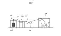
図2は、一括めっき部42の形成を説明する図である。まず、一括めっき部42の形成に先立ち、絶縁体3の周囲に複数本の金属素線411を撚り合わせて横巻きシールド部41を形成する。絶縁体3の周囲に横巻きシールド部41を形成したものをケーブル基体101と呼称する。一括めっき部42を形成する際は、まず、送り出し装置102にケーブル基体101を巻き付けたドラム102aをセットし、送り出し装置102からケーブル基体101を送り出す。送り出し装置102から送り出されたケーブル基体101は、フラックス槽103に導入され、ケーブル基体101の周囲(すなわち横巻きシールド部41の周囲)に、フラックスが塗布される。フラックスは、横巻きシールド部41の周囲全体に溶融した錫が一括して付着しやすくするためのものであり、例えば、ロジン系のフラックス等を用いることができる。フラックス槽103を通過したケーブル基体101は、250℃以上300℃未満の温度に溶融した錫を貯留しためっき槽104に導入され、ダイス105を通過する。ダイス105の通過後に残った錫が冷却されることで、一括めっき部42が形成される。すなわち、一括めっき部42は、溶融めっきによって形成された溶融めっき層である。その後、一括めっき部42を形成したケーブル基体101を、巻き取り機106で巻き取る。なお、横巻きシールド部41が形成されたケーブル基体101をめっき槽104に通すときの線速度は、例えば、40m/min以上80m/min以下であり、より好ましくは、50m/min以上70m/min以下である。 FIG. 2 is a diagram illustrating the formation of the
一括めっき部42を形成する際、溶融した錫(すなわち、溶融めっき)に接触する部分のめっき層411bを構成する銀はめっき槽104内の錫に拡散し、金属素線411と一括めっき部42との間(すなわち、金属線411aと一括めっき部42との間であって、当該金属線411の表面と接する部分)に銅と錫を含む金属間化合物411cが形成される。本発明者らがSEM(走査型電子顕微鏡)を用いたEDX分析(エネルギー分散型X線分光法による分析)を行ったところ、金属素線411の表面(金属素線411と一括めっき部42との間)に、銅と錫とからなる金属間化合物411cが層状に存在することが確認できた。すなわち、金属間化合物411cは、溶融めっきからなる一括めっき部42を構成する金属元素(錫等)と金属素線411の主成分を構成する金属元素(銅等)とが金属的に拡散反応して金属素線411の表面に化合物層が形成されたものである。金属間化合物411cの層の厚さは、例えば0.2μm~1.5μm程度である。なお、金属間化合物411cには、めっき層411bを構成する銀が含まれていると考えられるが、金属間化合物411cにおける銀の含有量は、EDX分析で検出が難しい程度のごく微量である。 When forming the
シールド層4は、金属素線411と一括めっき部42との間に金属間化合物411cが形成されることにより、同軸ケーブル1を繰り返し曲げたときや捩ったときに、金属素線411の表面から一括めっき部42が剥がれにくく、金属素線411と一括めっき部42との間に隙間が生じにくくなる。これにより、同軸ケーブル1では、曲げや捩りが加わった場合にも、横巻シールド部41の外側から一括めっき部42によって横巻シールド部41を固定した状態を保つことができ、シールド層4と導体2との距離が変化しにくくなる。そのため、同軸ケーブル1では、曲げや捩りによってシールド効果の低下が生じにくく、所定の周波数帯域で急激な減衰も生じにくくすることができる。金属間化合物411cの層の厚さは、例えば、光学顕微鏡あるいは電子顕微鏡を用いて、同軸ケーブル1の横断面(同軸ケーブル1の長手方向に垂直な断面)を観察することにより求められる。 The
一括めっき部42と接触しない部分の金属素線411(めっき時に溶融した錫と接触しない部分の金属素線411)には、銀からなるめっき層411bが残存する。すなわち、ケーブル径方向において内側(絶縁体3側)の部分の金属素線411には、銀からなるめっき層411bが残存する。すなわち、本実施の形態に係る同軸ケーブル1におけるシールド層4は、複数の金属素線411が一括めっき部4によって覆われる外周部分4aよりも、複数の金属素線411が一括めっき部41で覆われておらずめっき層411bが露出した内周部分4bの導電率が高くなっている。高周波信号の伝送においては、電流はシールド層4における絶縁体3側に集中するため、銀等の高い導電率を有するめっき層411bがシールド層4の内周部分4bに存在することにより、シールド層4の導電性の低下を抑制し、良好な減衰特性を維持することが可能になる。一括めっき部42を構成する錫めっきの導電率は15%IACSであり、めっき層411bを構成する銀めっきの導電率は108%IACSである。 A
なお、ここでいう外周部分4aとは、金属素線411が溶融めっき時に溶融しためっき(錫等)に接触する部分(すなわち金属間化合物411cが形成された部分)である。また、内周部分4bとは、銀めっき等からなるめっき層411bが残存している部分である。 The outer
(連結部43の説明)
シールド層4は、周方向に隣り合う金属素線同士が離間している離間部分45を有している。なお、全ての金属素線411が離間している必要はなく、周方向に隣り合う一部の金属素線411同士が接触している接触部分が存在してもよい。なお、接触部分では、横巻きシールド部41の外周において、周方向に隣り合う金属素線411同士の間が一括めっき部42によって充填された充填部を有する。(Description of the connecting part 43)
The
そして、シールド層4は、周方向に隣り合う金属素線411同士が一括めっき部42により連結されている連結部43を有している。一括めっき部42は、周方向および軸方向において横巻きシールド部41の周囲全体を一括して覆い、複数の金属素線411を機械的及び電気的に接続するように設けられることが望ましい。本実施の形態に係る同軸ケーブル1のシールド層4では、隣り合う内周部分4bの間に連結部43が設けられている。内周部分4bの周囲は一括めっき部42により覆われていないため、隣り合う金属素線411の内周部分4b同士の間で、かつ、絶縁体3の外面と一括めっき部42(連結部43)の内面との間には、空気層44が存在する。この空気層44に関し、絶縁体3の外面と対向する連結部43の内面は、連結部43の内部側へ凹むように湾曲した形状を有している。このような湾曲した形状を有することにより、絶縁体3の外面と連結部43の内面との間に所定の大きさの空気層44を設けることができるため、シールド効果の低下が生じにくく、所定の周波数帯域(例えば、26GHzまでの周波数帯域)で急激な減衰が生じにくい同軸ケーブル1とすることができる。 The
図3は、同軸ケーブル1を実際に試作し、シールド層4を剥がして観察した際の写真及びその拡大写真である。図3に示すように、本実施の形態では、シールド層4の少なくとも一部において、ケーブル径方向内側(絶縁体3の表面からシールド層4へ向かう方向)から見て、連結部32を構成する一括めっき部42と、内周部分4bで露出するめっき層411bとが、金属素線411の長手方向に対して垂直な方向に交互に配置されている。すなわち、シールド層4を径方向内側から見ると、一括めっき部42を構成する錫と、めっき層411bを構成する銀とが、縞状に交互に配置された状態となっている。 FIG. 3 shows a photograph and an enlarged photograph of the coaxial cable 1 actually produced as a prototype and observed after peeling off the
隣り合う内周部分4bの間に連結部43を有することにより、例えば周方向に隣り合う全ての金属素線411同士が接触する場合と比べて、曲げや捩れを加えたときに一括めっき部42が割れたり剥がれたりしにくくなる。すなわち、金属素線441同士が離間している部分が一括めっき部42によって連結された連結部43は、金属素線411よりも柔軟性のある溶融めっきからなる一括めっき部42のみで構成される。曲げや捻回が加わったときに、連結部分の一括めっき部42が伸張するように作用し、シールド層4全体の柔軟性が向上する。これにより、曲げや捩れを加えたときに一括めっき部42が割れたり剥がれたりしにくくなる。なお、周方向に隣り合う金属素線411同士が離間する距離は、一方の金属素線411の表面から他方の金属素線411までの最短距離が金属素線411の外径の半分以下であると、上述した作用効果が得られやすい。 By having the connecting
また、連結部43における一括めっき部42の径方向に沿った厚さW(連結部43における一括めっき部42の内面から外面までの最小の直線距離)は、例えば、金属素線411の外径(直径)dの30%(0.3×d)以上であると、一括めっき部42の割れが生じにくくなる。特に、連結部43における一括めっき部42の厚さWは、金属素線411の外径(直径)dと同じか、それよりも大きい場合に、金属素線411同士の接合強度が大きくなり、更に割れが生じにくくなる。また、同軸ケーブル1では、一括めっき部42が上述したような連結部43を有することにより、ケーブルアセンブリを行うときに、横巻シールド部41を構成する複数の金属素線411が一括めっき部42にくっついた状態で、複数の金属素線411の巻き方向に沿って螺旋状に巻き回しながらシールド層4が除去しやすくなる。連結部43における一括めっき部42の厚さWの上限値としては、例えば、金属素線411の外径dの130%(1.3×d)であるとよい。なお、金属素線411の外径dは、例えば、0.02mm~0.10mmである。連結部43の厚さWや金属素線411の外径dは、例えば、光学顕微鏡あるいは電子顕微鏡を用いて、同軸ケーブル1の横断面(同軸ケーブル1の長手方向に垂直な断面)を観察することにより求められる。 Further, the thickness W along the radial direction of the
例えば、シールド層4を横巻きシールド部41のみで構成すると、金属素線411間に隙間が発生してノイズ特性が低下してしまう。さらに、金属素線411の間に生じる隙間の影響により、所定の周波数帯域(例えば、10GHz~25GHzの帯域)で急激な減衰が生じるサックアウトと呼ばれる現象が発生してしまう。本実施の形態のように、横巻きシールド部41の周囲全体を覆うように溶融めっきからなる一括めっき部42を設けることで、一括めっき部42により金属素線411間の隙間を塞ぐことができ、シールド効果を向上できる。これにより、信号伝送の損失が生じにくくなる。さらに、金属素線411間の隙間がなくなることにより、サックアウトの発生を抑制することが可能になる。 For example, if the
さらに、横巻きシールド部41の周囲を覆うように一括めっき部42を設けることで、端末加工時にケーブル端末部においてシース5を除去しシールド層4を露出させた際に、金属素線411が解けにくくなり、端末加工を容易に行うことが可能になる。さらにまた、横巻きシールド部41の周囲を覆うように一括めっき部42を設けることで、ケーブル長手方向においてインピーダンスを安定して一定に維持することも可能になる。 Furthermore, by providing the
図4(a)は、絶縁体3から剥がしたシールド層4において銀が存在する領域を分析した結果を示す写真であり、図4(b)は剥がしたシールド層4において錫が存在する領域を分析した結果を示す写真である。図4(a),(b)とも、剥がしたシールド層4をケーブル径方向内側から観察した状態を示しており、両者の縮尺は同じとなっている。図4(a)では、色が薄い部分が銀(Ag)が存在している領域を表しており、図4(b)では、色が薄い部分が錫(Sn)が存在している領域を表している。なお、図4(a),(b)は、SEMを用いたEDX分析から得られるデータを元素マッピングすることにより得られたものである。Figure 4(a) is a photograph showing the results of analyzing the area where silver is present in the
図4(a),(b)に示すように、シールド層4では、ケーブル径方向内側から見て、銀(Ag)が存在している領域の幅が、錫(Sn)が存在している領域の幅よりも大きくなっている。すなわち、本実施の形態では、ケーブル径方向内側から見て、内周部分4bで露出するめっき層411bの幅が、連結部43を構成する一括めっき部42の幅よりも大きくなっている。ここでいう幅とは、めっき層411bと一括めっき部42の配列方向(図4(a),(b)の上下方向)における幅であり、金属素線411の長手方向に対して垂直な方向の幅をいう。 As shown in FIGS. 4(a) and 4(b), in the
絶縁体3側からシールド層4に電流(シールド電流)が流れる際、このシールド電流が、導電率が高い銀からなるめっき層411bへと流れた方が、損失が小さくなり、伝送特性が向上する。そのため、本実施の形態のように、ケーブル径方向内側から見て、めっき層411bの幅を、一括めっき部42(連結部43)の幅よりも大きくすることで、シールド電流がめっき層411bへと流れやすくなり、伝送特性を向上させることが可能になる。特に、めっき層411bの幅が大きいほど、内周部分4bの領域が大きくなり、絶縁体3から一括めっき部42(連結部43)の内面までの距離が遠くなるため、錫からなる一括めっき部42にシールド電流が流れにくくなり、伝送特性がより向上する。 When a current (shield current) flows from the
(同軸ケーブル1の特性評価)
本実施の形態に係る同軸ケーブル1を作製して実施例とし、周波数特性の評価を行った。ケーブル長は、1mとした。また、実施例における同軸ケーブル1では、導体2として外径が0.023mmの軟銅線からなる金属素線21を7本撚り合わせたものを用い、絶縁体3としてPFA(パーフルオロアルコキシアルカン)をチューブ押出ししてなるものを用い、横巻きシールド部41として外径が0.025mm(43AWG)で表面に銀めっきを有する金属素線411を22本螺旋状に巻き付けしたものを用い、一括めっき部42として溶融した錫からなる溶融めっきを用い、シース5としてフッ素樹脂からなるものを用いた。周波数特性の評価では、ネットワークアナライザを用いて、伝送特性S21の測定を行った。測定範囲は10MHz~30GHzとし、出力パワーは-8dBmとした。測定結果を図5に示す。(Characteristics evaluation of coaxial cable 1)
A coaxial cable 1 according to the present embodiment was manufactured as an example, and its frequency characteristics were evaluated. The cable length was 1 m. In addition, in the coaxial cable 1 in the example, the
図5に示すように、実施例の同軸ケーブル1では、20GHz以降まで(例えば、26GHzまで)急激な減衰がみられず、サックアウトが抑制されていることが確認できた。図5の結果より、少なくとも25GHz以下の周波数帯域において、サックアウトフリーとなっていることが確認できた。 As shown in FIG. 5, in the coaxial cable 1 of the example, no rapid attenuation was observed up to 20 GHz or higher (for example, up to 26 GHz), and it was confirmed that suckout was suppressed. From the results shown in FIG. 5, it was confirmed that there was no suckout at least in the frequency band of 25 GHz or less.
(ケーブルアセンブリ)
次に、同軸ケーブル1を用いたケーブルアセンブリについて説明する。図6は、本実施の形態に係るケーブルアセンブリの端末部を示す断面図である。(cable assembly)
Next, a cable assembly using the coaxial cable 1 will be explained. FIG. 6 is a sectional view showing the terminal portion of the cable assembly according to this embodiment.
図6に示すように、ケーブルアセンブリ10は、本実施の形態に係る同軸ケーブル1と、同軸ケーブル1の少なくとも一方の端部に一体に設けられた端末部材11と、を備えている。 As shown in FIG. 6, the
端末部材11は、例えば、コネクタ、センサ、コネクタやセンサ内に搭載される基板、あるいは電子機器内の基板等である。図6では、端末部材11が基板11aである場合を示している。基板11aには、導体2が接続される信号電極12、及び、シールド層4が接続されるグランド電極13が形成されている。基板11aは、樹脂からなる基材16に信号電極12及びグランド電極13を含む導体パターンが印刷されたプリント基板からなる。 The
同軸ケーブル1の端末部においては、端末から所定長さの部分のシース5が除去されシールド層4が露出されており、さらに露出されたシールド層4及び絶縁体3の端末部が除去され導体2が露出されている。露出された導体2が半田等の接続材14によって信号電極12に固定され、導体2が信号電極12に電気的に接続されている。また、露出されたシールド層4が半田等の接続材15によってグランド電極13に固定され、シールド層4がグランド電極13に電気的に接続されている。なお、導体2やシールド層4の接続は半田等の接続材14,15を用いずともよく、例えば、固定用の金具に導体2やシールド層4を加締め等により固定することで、導体2やシールド層4を接続してもよい。また、端末部材11がコネクタやセンサである場合、導体2やシールド層4を直接電極や素子に接続する構成としてもよい。At the terminal of the coaxial cable 1, a predetermined length of the
(実施の形態の作用及び効果)
以上説明したように、本実施の形態に係る同軸ケーブル1では、シールド層4は、絶縁体3の周囲を覆うように複数の金属素線411が螺旋状に巻き付けされた横巻きシールド部41と、横巻きシールド部41の周囲を覆う溶融めっきからなる一括めっき部42と、を有し、シールド層4は、周方向に隣り合う金属素線411同士が離間している離間部分45において、周方向に隣り合う金属素線411同士が一括めっき部42により連結されている連結部43を有し、かつ、シールド層4は、複数の金属素線411が一括めっき部42で覆われておらずめっき層411bが露出した内周部分4bを有し、隣り合う内周部分4bの間に連結部43が設けられている。(Actions and effects of embodiments)
As explained above, in the coaxial cable 1 according to the present embodiment, the
このように構成することで、シールド層4が一括めっき部42を介して略全周で繋がることになり、横巻きシールド部41の金属素線411間の隙間を一括めっき部42で塞ぐことが可能になり、ノイズ特性を向上し、サックアウトの発生を抑制することが可能になる。すなわち、本実施の形態によれば、シールド効果の低下が生じにくく、所定の周波数帯域(例えば、26GHzまでの周波数帯域)で急激な減衰が生じにくい同軸ケーブル1を実現できる。さらに、金属素線411同士の間に入り込むように一括めっき部42が設けられることで、金属素線411同士の接合強度を向上でき、また、一括めっき部42が剥がれにくくなる。 With this configuration, the
(実施の形態のまとめ)
次に、以上説明した実施の形態から把握される技術思想について、実施の形態における符号等を援用して記載する。ただし、以下の記載における各符号等は、特許請求の範囲における構成要素を実施の形態に具体的に示した部材等に限定するものではない。(Summary of embodiments)
Next, technical ideas understood from the embodiments described above will be described using reference numerals and the like in the embodiments. However, each reference numeral in the following description does not limit the constituent elements in the claims to those specifically shown in the embodiments.
[1]導体(2)と、前記導体(2)の周囲を覆う絶縁体(3)と、前記絶縁体(3)の周囲を覆うシールド層(4)と、前記シールド層(4)の周囲を覆うシース(5)と、を備え、前記シールド層(4)は、最外層にめっき層(411b)を有する複数の金属素線(411)を前記絶縁体(3)の周囲に螺旋状に巻き付けて構成された横巻きシールド部(41)と、前記横巻きシールド部(41)の周囲を覆う溶融めっきからなる一括めっき部(42)と、を有し、前記シールド層(4)は、周方向に隣り合う前記金属素線(411)同士が離間している離間部分(45)において、周方向に隣り合う前記金属素線(411)同士が前記一括めっき部(42)により連結されている連結部(43)を有し、かつ、前記シールド層(4)は、前記複数の金属素線(411)が前記一括めっき部(42)で覆われておらず前記めっき層(411b)が露出した内周部分(4b)を有し、隣り合う前記内周部分(4b)の間に前記連結部(43)が設けられている、同軸ケーブル(1)。[1] A conductor (2), an insulator (3) that covers the periphery of the conductor (2), a shield layer (4) that covers the periphery of the insulator (3), and a periphery of the shield layer (4) a sheath (5) that covers the insulator (3), and the shield layer (4) includes a plurality of metal wires (411) having a plating layer (411b) on the outermost layer in a spiral shape around the insulator (3). The shield layer (4) has a horizontally wound shield portion (41) configured by winding it, and a bulk plating portion (42) made of hot-dip plating that covers the periphery of the horizontally wound shield portion (41), and the shield layer (4) includes: In the separated portion (45) where the circumferentially adjacent metal wires (411) are separated from each other, the circumferentially adjacent metal wires (411) are connected by the bulk plating portion (42). and the shield layer (4) has a connecting portion (43) in which the plurality of metal wires (411) are not covered with the bulk plating portion (42) and the plating layer (411b) is A coaxial cable (1) having an exposed inner circumferential portion (4b), and the connecting portion (43) is provided between adjacent inner circumferential portions (4b).
[2]前記シールド層(4)の少なくとも一部において、ケーブル径方向内側から見て、前記連結部(43)を構成する前記一括めっき部(42)と、前記内周部分(4b)で露出する前記めっき層(411b)とが、前記金属素線(411)の長手方向に対して垂直な方向に交互に配置されている、[1]に記載の同軸ケーブル(1)。[2] At least a portion of the shield layer (4) is exposed at the bulk plating portion (42) constituting the connecting portion (43) and the inner peripheral portion (4b) when viewed from inside in the cable radial direction. The coaxial cable (1) according to [1], wherein the plating layers (411b) are arranged alternately in a direction perpendicular to the longitudinal direction of the metal wire (411).
[3]ケーブル径方向内側から見て、前記内周部分(4b)で露出する前記めっき層(411b)の幅が、前記連結部(43)を構成する前記一括めっき部(42)の幅よりも大きい、[2]に記載の同軸ケーブル(1)。[3] When viewed from inside in the radial direction of the cable, the width of the plating layer (411b) exposed at the inner peripheral portion (4b) is greater than the width of the bulk plating portion (42) constituting the connecting portion (43). The coaxial cable (1) described in [2] is also large.
[4]前記めっき層(411b)の導電率が、前記一括めっき部(42)の導電率よりも高い、[1]乃至[3]の何れか1項に記載の同軸ケーブル(1)。[4] The coaxial cable (1) according to any one of [1] to [3], wherein the electrical conductivity of the plating layer (411b) is higher than the electrical conductivity of the bulk plating portion (42).
[5]前記めっき層(411b)が銀からなり、前記一括めっき部(42)が錫からなる、[1]乃至[4]の何れか1項に記載の同軸ケーブル(1)。[5] The coaxial cable (1) according to any one of [1] to [4], wherein the plating layer (411b) is made of silver, and the bulk plating part (42) is made of tin.
[6]前記シールド層(4)は、前記複数の金属素線(411)が前記一括めっき部(42)によって覆われる外周部分(4a)を有し、前記外周部分(4a)は、前記複数の金属素線(411)と前記一括めっき部(42)との間に金属間化合物(411c)を有する、[1]乃至[5]の何れか1項に記載の同軸ケーブル(1)。[6] The coaxial cable (1) described in any one of [1] to [5], wherein the shield layer (4) has an outer peripheral portion (4a) in which the plurality of metal wires (411) are covered by the collective plating portion (42), and the outer peripheral portion (4a) has an intermetallic compound (411c) between the plurality of metal wires (411) and the collective plating portion (42).
[7][1]乃至[6]の何れか1項に記載の同軸ケーブル(1)と、前記同軸ケーブル(1)の少なくとも一方の端部に一体に設けられた端末部材(11)と、を備えた、ケーブルアセンブリ(10)。[7] A cable assembly (10) comprising a coaxial cable (1) according to any one of [1] to [6] and a terminal member (11) integrally provided on at least one end of the coaxial cable (1).
以上、本発明の実施の形態を説明したが、上記に記載した実施の形態は特許請求の範囲に係る発明を限定するものではない。また、実施の形態の中で説明した特徴の組合せの全てが発明の課題を解決するための手段に必須であるとは限らない点に留意すべきである。また、本発明は、その趣旨を逸脱しない範囲で適宜変形して実施することが可能である。 Although the embodiments of the present invention have been described above, the embodiments described above do not limit the invention according to the claims. Furthermore, it should be noted that not all combinations of features described in the embodiments are essential for solving the problems of the invention. Moreover, the present invention can be implemented with appropriate modifications within a range that does not depart from the spirit thereof.
1…同軸ケーブル
2…導体
3…絶縁体
4…シールド層
4a…外周部分
4b…内周部分
41…横巻きシールド部
411…金属素線
411a…金属線
411b…めっき層
411c…金属間化合物
42…一括めっき部
4a…外周部分
4b…内周部分
43…連結部
45…離間部分
5…シース
10…ケーブルアセンブリ
11…端末部材1...
Claims (5)
Translated fromJapanese前記導体の周囲を覆う絶縁体と、
前記絶縁体の周囲を覆うシールド層と、
前記シールド層の周囲を覆うシースと、を備え、
前記シールド層は、最外層にめっき層を有する複数の金属素線を前記絶縁体の周囲に螺旋状に巻き付けて構成された横巻きシールド部と、前記横巻きシールド部の周囲を覆う溶融めっきからなる一括めっき部と、を有し、
前記シールド層は、周方向に隣り合う前記金属素線同士が離間している離間部分において、周方向に隣り合う前記金属素線同士が前記一括めっき部により連結されている連結部を有し、
かつ、前記シールド層は、前記複数の金属素線が前記一括めっき部で覆われておらず前記めっき層が露出した内周部分を有し、
隣り合う前記内周部分の間に前記連結部が設けられており、
前記シールド層の少なくとも一部において、ケーブル径方向内側から見て、前記連結部を構成する前記一括めっき部と、前記内周部分で露出する前記めっき層とは、前記金属素線の長手方向に対して垂直な方向に交互に配置されており、
ケーブル径方向内側から見て、前記内周部分で露出する前記めっき層の幅は、前記連結部を構成する前記一括めっき部の幅よりも大きい、
同軸ケーブル。 a conductor;
an insulator surrounding the conductor;
a shield layer surrounding the insulator;
A sheath that covers the periphery of the shield layer,
The shield layer includes a horizontally wound shield portion formed by spirally winding a plurality of metal wires having a plating layer on the outermost layer around the insulator, and a hot-dip plating that covers the periphery of the horizontally wound shield portion. It has a bulk plating part,
The shield layer has a connecting portion in which the metal wires adjacent in the circumferential direction are connected by the bulk plating portion in a spaced apart portion where the metal wires adjacent in the circumferential direction are separated from each other,
and the shield layer has an inner peripheral portion where the plurality of metal wires are not covered with the bulk plating part and the plating layer is exposed,
The connecting portionis provided between the adjacent inner peripheral portions,
In at least a portion of the shield layer, when viewed from inside in the radial direction of the cable, the bulk plating portion constituting the connecting portion and the plating layer exposed at the inner peripheral portion are arranged in the longitudinal direction of the metal wire. They are arranged alternately in the direction perpendicular to the
When viewed from inside in the cable radial direction, the width of the plating layer exposed at the inner peripheral portion is larger than the width of the bulk plating portion constituting the connecting portion.
coaxial cable.
請求項1に記載の同軸ケーブル。 The electricalconductivity of the plating layer is higher than the electrical conductivity of the bulk plating part,
The coaxial cable according to claim1 .
請求項1又は2に記載の同軸ケーブル。 The plating layeris made of silver, and the bulk plating partis made of tin.
The coaxial cable according to claim 1or 2 .
前記外周部分は、前記複数の金属素線と前記一括めっき部との間に金属間化合物を有する、
請求項1乃至3の何れか1項に記載の同軸ケーブル。 The shield layer has an outer peripheral portion where the plurality of metal wires are covered by the bulk plating part,
The outer peripheral portion has an intermetallic compound between the plurality of metal wires and the bulk plating part,
The coaxial cable according to any one of claims 1 to3 .
前記同軸ケーブルの少なくとも一方の端部に一体に設けられた端末部材と、を備えた、
ケーブルアセンブリ。
The coaxial cable according to any one of claims 1 to4 ,
a terminal member integrally provided at at least one end of the coaxial cable;
cable assembly.
Priority Applications (4)
| Application Number | Priority Date | Filing Date | Title |
|---|---|---|---|
| JP2020155003AJP7456337B2 (en) | 2020-09-15 | 2020-09-15 | Coaxial cables and cable assemblies |
| US17/410,770US11715584B2 (en) | 2020-09-15 | 2021-08-24 | Coaxial cable and cable assembly |
| KR1020210111605AKR102857480B1 (en) | 2020-09-15 | 2021-08-24 | Coaxial cable and cable assembly |
| CN202110989957.3ACN114188088A (en) | 2020-09-15 | 2021-08-26 | Coaxial cable and cable assembly |
Applications Claiming Priority (1)
| Application Number | Priority Date | Filing Date | Title |
|---|---|---|---|
| JP2020155003AJP7456337B2 (en) | 2020-09-15 | 2020-09-15 | Coaxial cables and cable assemblies |
Publications (2)
| Publication Number | Publication Date |
|---|---|
| JP2022048924A JP2022048924A (en) | 2022-03-28 |
| JP7456337B2true JP7456337B2 (en) | 2024-03-27 |
Family
ID=80844372
Family Applications (1)
| Application Number | Title | Priority Date | Filing Date |
|---|---|---|---|
| JP2020155003AActiveJP7456337B2 (en) | 2020-09-15 | 2020-09-15 | Coaxial cables and cable assemblies |
Country Status (1)
| Country | Link |
|---|---|
| JP (1) | JP7456337B2 (en) |
Families Citing this family (1)
| Publication number | Priority date | Publication date | Assignee | Title |
|---|---|---|---|---|
| JP7533141B2 (en) | 2020-11-12 | 2024-08-14 | 株式会社プロテリアル | Coaxial Cables and Cable Assemblies |
Citations (2)
| Publication number | Priority date | Publication date | Assignee | Title |
|---|---|---|---|---|
| JP2003045244A (en) | 2001-08-03 | 2003-02-14 | Hitachi Cable Ltd | Semi-flexible micro coaxial cable and method for connecting its terminals |
| JP2014191884A (en) | 2013-03-26 | 2014-10-06 | Hitachi Metals Ltd | Coaxial cable and method for manufacturing the same |
Family Cites Families (1)
| Publication number | Priority date | Publication date | Assignee | Title |
|---|---|---|---|---|
| JP3013637B2 (en)* | 1992-12-28 | 2000-02-28 | 住友電気工業株式会社 | High frequency coaxial cable and method of manufacturing the same |
- 2020
- 2020-09-15JPJP2020155003Apatent/JP7456337B2/enactiveActive
Patent Citations (2)
| Publication number | Priority date | Publication date | Assignee | Title |
|---|---|---|---|---|
| JP2003045244A (en) | 2001-08-03 | 2003-02-14 | Hitachi Cable Ltd | Semi-flexible micro coaxial cable and method for connecting its terminals |
| JP2014191884A (en) | 2013-03-26 | 2014-10-06 | Hitachi Metals Ltd | Coaxial cable and method for manufacturing the same |
Also Published As
| Publication number | Publication date |
|---|---|
| JP2022048924A (en) | 2022-03-28 |
Similar Documents
| Publication | Publication Date | Title |
|---|---|---|
| JP7148011B2 (en) | Coaxial cable and cable assembly | |
| US11631507B2 (en) | Coaxial cable, coaxial cable producing method, and cable assembly | |
| KR102857480B1 (en) | Coaxial cable and cable assembly | |
| JP7081699B2 (en) | Coaxial cable and cable assembly | |
| US11955256B2 (en) | Signal transmission cable | |
| JP7456337B2 (en) | Coaxial cables and cable assemblies | |
| JP6901034B1 (en) | Coaxial cable and cable assembly | |
| JP7585998B2 (en) | Signal transmission cables and cable assemblies | |
| JP7533141B2 (en) | Coaxial Cables and Cable Assemblies | |
| JP7694430B2 (en) | Flat Cable | |
| JP2023045115A (en) | Coaxial cable and multicore cable | |
| JP7243499B2 (en) | High-frequency signal transmission cable and its manufacturing method | |
| JP6261229B2 (en) | coaxial cable | |
| CN118053616A (en) | Composite cable |
Legal Events
| Date | Code | Title | Description |
|---|---|---|---|
| A621 | Written request for application examination | Free format text:JAPANESE INTERMEDIATE CODE: A621 Effective date:20230210 | |
| A977 | Report on retrieval | Free format text:JAPANESE INTERMEDIATE CODE: A971007 Effective date:20231005 | |
| A131 | Notification of reasons for refusal | Free format text:JAPANESE INTERMEDIATE CODE: A131 Effective date:20231024 | |
| A521 | Request for written amendment filed | Free format text:JAPANESE INTERMEDIATE CODE: A523 Effective date:20231213 | |
| TRDD | Decision of grant or rejection written | ||
| A01 | Written decision to grant a patent or to grant a registration (utility model) | Free format text:JAPANESE INTERMEDIATE CODE: A01 Effective date:20240213 | |
| A61 | First payment of annual fees (during grant procedure) | Free format text:JAPANESE INTERMEDIATE CODE: A61 Effective date:20240226 | |
| R150 | Certificate of patent or registration of utility model | Ref document number:7456337 Country of ref document:JP Free format text:JAPANESE INTERMEDIATE CODE: R150 |