JP7447213B2 - semiconductor equipment - Google Patents
semiconductor equipmentDownload PDFInfo
- Publication number
- JP7447213B2 JP7447213B2JP2022162377AJP2022162377AJP7447213B2JP 7447213 B2JP7447213 B2JP 7447213B2JP 2022162377 AJP2022162377 AJP 2022162377AJP 2022162377 AJP2022162377 AJP 2022162377AJP 7447213 B2JP7447213 B2JP 7447213B2
- Authority
- JP
- Japan
- Prior art keywords
- oxide semiconductor
- layer
- thin film
- oxide
- film transistor
- Prior art date
- Legal status (The legal status is an assumption and is not a legal conclusion. Google has not performed a legal analysis and makes no representation as to the accuracy of the status listed.)
- Active
Links
- 239000004065semiconductorSubstances0.000titleclaimsdescription460
- 230000015572biosynthetic processEffects0.000claimsdescription38
- 230000006870functionEffects0.000claimsdescription31
- 239000010410layerSubstances0.000description700
- 239000010409thin filmSubstances0.000description290
- 239000010408filmSubstances0.000description244
- 239000000758substrateSubstances0.000description106
- 238000000034methodMethods0.000description81
- 239000004973liquid crystal related substanceSubstances0.000description49
- 239000000463materialSubstances0.000description45
- 238000004544sputter depositionMethods0.000description44
- 229910007541Zn OInorganic materials0.000description40
- 239000013078crystalSubstances0.000description37
- 238000010586diagramMethods0.000description36
- 238000005530etchingMethods0.000description33
- XLOMVQKBTHCTTD-UHFFFAOYSA-NZinc monoxideChemical compound[Zn]=OXLOMVQKBTHCTTD-UHFFFAOYSA-N0.000description27
- 238000004519manufacturing processMethods0.000description27
- VYPSYNLAJGMNEJ-UHFFFAOYSA-NSilicium dioxideChemical compoundO=[Si]=OVYPSYNLAJGMNEJ-UHFFFAOYSA-N0.000description26
- 230000001681protective effectEffects0.000description26
- 229910052814silicon oxideInorganic materials0.000description26
- IJGRMHOSHXDMSA-UHFFFAOYSA-NAtomic nitrogenChemical compoundN#NIJGRMHOSHXDMSA-UHFFFAOYSA-N0.000description22
- 239000011159matrix materialSubstances0.000description20
- 230000008569processEffects0.000description20
- 239000000123paperSubstances0.000description19
- 239000002245particleSubstances0.000description19
- XKRFYHLGVUSROY-UHFFFAOYSA-NArgonChemical compound[Ar]XKRFYHLGVUSROY-UHFFFAOYSA-N0.000description18
- 229910052581Si3N4Inorganic materials0.000description17
- 239000004020conductorSubstances0.000description17
- HQVNEWCFYHHQES-UHFFFAOYSA-Nsilicon nitrideChemical compoundN12[Si]34N5[Si]62N3[Si]51N64HQVNEWCFYHHQES-UHFFFAOYSA-N0.000description17
- 239000012298atmosphereSubstances0.000description16
- 239000003990capacitorSubstances0.000description16
- 230000037230mobilityEffects0.000description16
- 238000000206photolithographyMethods0.000description16
- 229910052782aluminiumInorganic materials0.000description15
- 239000011701zincSubstances0.000description15
- 239000011787zinc oxideSubstances0.000description15
- XAGFODPZIPBFFR-UHFFFAOYSA-NaluminiumChemical compound[Al]XAGFODPZIPBFFR-UHFFFAOYSA-N0.000description14
- 239000007789gasSubstances0.000description14
- 229910052760oxygenInorganic materials0.000description13
- XUIMIQQOPSSXEZ-UHFFFAOYSA-NSiliconChemical compound[Si]XUIMIQQOPSSXEZ-UHFFFAOYSA-N0.000description12
- 239000001301oxygenSubstances0.000description12
- 229910052710siliconInorganic materials0.000description12
- 239000010703siliconSubstances0.000description12
- 239000002356single layerSubstances0.000description12
- 239000000203mixtureSubstances0.000description11
- 229910052757nitrogenInorganic materials0.000description11
- 239000012071phaseSubstances0.000description11
- RTAQQCXQSZGOHL-UHFFFAOYSA-NTitaniumChemical compound[Ti]RTAQQCXQSZGOHL-UHFFFAOYSA-N0.000description10
- QVGXLLKOCUKJST-UHFFFAOYSA-Natomic oxygenChemical compound[O]QVGXLLKOCUKJST-UHFFFAOYSA-N0.000description10
- 239000000969carrierSubstances0.000description10
- 229920005989resinPolymers0.000description10
- 239000011347resinSubstances0.000description10
- 239000000126substanceSubstances0.000description10
- 229910052719titaniumInorganic materials0.000description10
- 239000010936titaniumSubstances0.000description10
- 229910052725zincInorganic materials0.000description10
- 229910004298SiO 2Inorganic materials0.000description9
- 229910052786argonInorganic materials0.000description9
- 239000001257hydrogenSubstances0.000description9
- 229910052739hydrogenInorganic materials0.000description9
- 229910052738indiumInorganic materials0.000description9
- 239000003094microcapsuleSubstances0.000description9
- MYMOFIZGZYHOMD-UHFFFAOYSA-NDioxygenChemical compoundO=OMYMOFIZGZYHOMD-UHFFFAOYSA-N0.000description8
- UFHFLCQGNIYNRP-UHFFFAOYSA-NHydrogenChemical compound[H][H]UFHFLCQGNIYNRP-UHFFFAOYSA-N0.000description8
- 229910020923Sn-OInorganic materials0.000description8
- 238000004891communicationMethods0.000description8
- 229910001882dioxygenInorganic materials0.000description8
- 239000011521glassSubstances0.000description8
- PJXISJQVUVHSOJ-UHFFFAOYSA-Nindium(iii) oxideChemical compound[O-2].[O-2].[O-2].[In+3].[In+3]PJXISJQVUVHSOJ-UHFFFAOYSA-N0.000description8
- 238000001039wet etchingMethods0.000description8
- ZOKXTWBITQBERF-UHFFFAOYSA-NMolybdenumChemical compound[Mo]ZOKXTWBITQBERF-UHFFFAOYSA-N0.000description7
- 229910052779NeodymiumInorganic materials0.000description7
- 239000000956alloySubstances0.000description7
- 125000004429atomChemical group0.000description7
- 229920001940conductive polymerPolymers0.000description7
- 229910003437indium oxideInorganic materials0.000description7
- 229910052751metalInorganic materials0.000description7
- 239000007769metal materialSubstances0.000description7
- 229910052750molybdenumInorganic materials0.000description7
- 239000011733molybdenumSubstances0.000description7
- QEFYFXOXNSNQGX-UHFFFAOYSA-Nneodymium atomChemical compound[Nd]QEFYFXOXNSNQGX-UHFFFAOYSA-N0.000description7
- 229910052721tungstenInorganic materials0.000description7
- 239000010937tungstenSubstances0.000description7
- RYGMFSIKBFXOCR-UHFFFAOYSA-NCopperChemical compound[Cu]RYGMFSIKBFXOCR-UHFFFAOYSA-N0.000description6
- 229910052802copperInorganic materials0.000description6
- 239000010949copperSubstances0.000description6
- 230000005684electric fieldEffects0.000description6
- 229910052733galliumInorganic materials0.000description6
- AMGQUBHHOARCQH-UHFFFAOYSA-Nindium;oxotinChemical compound[In].[Sn]=OAMGQUBHHOARCQH-UHFFFAOYSA-N0.000description6
- 238000003780insertionMethods0.000description6
- 230000037431insertionEffects0.000description6
- 239000002184metalSubstances0.000description6
- 229910044991metal oxideInorganic materials0.000description6
- 150000004706metal oxidesChemical class0.000description6
- 239000011241protective layerSubstances0.000description6
- 239000000565sealantSubstances0.000description6
- 229910052718tinInorganic materials0.000description6
- WFKWXMTUELFFGS-UHFFFAOYSA-NtungstenChemical compound[W]WFKWXMTUELFFGS-UHFFFAOYSA-N0.000description6
- 150000001875compoundsChemical class0.000description5
- 238000002425crystallisationMethods0.000description5
- 230000008025crystallizationEffects0.000description5
- 238000001312dry etchingMethods0.000description5
- 239000000945fillerSubstances0.000description5
- 238000010438heat treatmentMethods0.000description5
- QGLKJKCYBOYXKC-UHFFFAOYSA-NnonaoxidotritungstenChemical compoundO=[W]1(=O)O[W](=O)(=O)O[W](=O)(=O)O1QGLKJKCYBOYXKC-UHFFFAOYSA-N0.000description5
- 230000003287optical effectEffects0.000description5
- 229920003023plasticPolymers0.000description5
- 239000004033plasticSubstances0.000description5
- 239000012798spherical particleSubstances0.000description5
- -1tungsten nitrideChemical class0.000description5
- 229910001930tungsten oxideInorganic materials0.000description5
- VYZAMTAEIAYCRO-UHFFFAOYSA-NChromiumChemical compound[Cr]VYZAMTAEIAYCRO-UHFFFAOYSA-N0.000description4
- 229910005191Ga 2 O 3Inorganic materials0.000description4
- VEXZGXHMUGYJMC-UHFFFAOYSA-NHydrochloric acidChemical compoundClVEXZGXHMUGYJMC-UHFFFAOYSA-N0.000description4
- GWEVSGVZZGPLCZ-UHFFFAOYSA-NTitan oxideChemical compoundO=[Ti]=OGWEVSGVZZGPLCZ-UHFFFAOYSA-N0.000description4
- 229910045601alloyInorganic materials0.000description4
- 239000012300argon atmosphereSubstances0.000description4
- 230000008901benefitEffects0.000description4
- 238000004364calculation methodMethods0.000description4
- 229910052804chromiumInorganic materials0.000description4
- 239000011651chromiumSubstances0.000description4
- KPUWHANPEXNPJT-UHFFFAOYSA-NdisiloxaneChemical class[SiH3]O[SiH3]KPUWHANPEXNPJT-UHFFFAOYSA-N0.000description4
- 239000000428dustSubstances0.000description4
- 239000007788liquidSubstances0.000description4
- 230000007246mechanismEffects0.000description4
- 239000002159nanocrystalSubstances0.000description4
- 150000004767nitridesChemical class0.000description4
- 125000004433nitrogen atomChemical groupN*0.000description4
- 125000004430oxygen atomChemical groupO*0.000description4
- 229910052706scandiumInorganic materials0.000description4
- SIXSYDAISGFNSX-UHFFFAOYSA-Nscandium atomChemical compound[Sc]SIXSYDAISGFNSX-UHFFFAOYSA-N0.000description4
- 229910052715tantalumInorganic materials0.000description4
- GUVRBAGPIYLISA-UHFFFAOYSA-Ntantalum atomChemical compound[Ta]GUVRBAGPIYLISA-UHFFFAOYSA-N0.000description4
- OGIDPMRJRNCKJF-UHFFFAOYSA-Ntitanium oxideInorganic materials[Ti]=OOGIDPMRJRNCKJF-UHFFFAOYSA-N0.000description4
- YVTHLONGBIQYBO-UHFFFAOYSA-Nzinc indium(3+) oxygen(2-)Chemical compound[O--].[Zn++].[In+3]YVTHLONGBIQYBO-UHFFFAOYSA-N0.000description4
- 229910000838Al alloyInorganic materials0.000description3
- MUBZPKHOEPUJKR-UHFFFAOYSA-NOxalic acidChemical compoundOC(=O)C(O)=OMUBZPKHOEPUJKR-UHFFFAOYSA-N0.000description3
- NRTOMJZYCJJWKI-UHFFFAOYSA-NTitanium nitrideChemical compound[Ti]#NNRTOMJZYCJJWKI-UHFFFAOYSA-N0.000description3
- NIXOWILDQLNWCW-UHFFFAOYSA-Nacrylic acid groupChemical groupC(C=C)(=O)ONIXOWILDQLNWCW-UHFFFAOYSA-N0.000description3
- 239000002585baseSubstances0.000description3
- 238000005229chemical vapour depositionMethods0.000description3
- KRKNYBCHXYNGOX-UHFFFAOYSA-Ncitric acidChemical compoundOC(=O)CC(O)(C(O)=O)CC(O)=OKRKNYBCHXYNGOX-UHFFFAOYSA-N0.000description3
- 229910010272inorganic materialInorganic materials0.000description3
- 150000002500ionsChemical class0.000description3
- 238000004020luminiscence typeMethods0.000description3
- 150000002894organic compoundsChemical class0.000description3
- TWNQGVIAIRXVLR-UHFFFAOYSA-Noxo(oxoalumanyloxy)alumaneChemical compoundO=[Al]O[Al]=OTWNQGVIAIRXVLR-UHFFFAOYSA-N0.000description3
- 238000005192partitionMethods0.000description3
- 229920006267polyester filmPolymers0.000description3
- 230000004044responseEffects0.000description3
- 238000005001rutherford backscattering spectroscopyMethods0.000description3
- 239000003566sealing materialSubstances0.000description3
- 238000004088simulationMethods0.000description3
- 239000007787solidSubstances0.000description3
- 238000003860storageMethods0.000description3
- WZJUBBHODHNQPW-UHFFFAOYSA-N2,4,6,8-tetramethyl-1,3,5,7,2$l^{3},4$l^{3},6$l^{3},8$l^{3}-tetraoxatetrasilocaneChemical compoundC[Si]1O[Si](C)O[Si](C)O[Si](C)O1WZJUBBHODHNQPW-UHFFFAOYSA-N0.000description2
- UWCWUCKPEYNDNV-LBPRGKRZSA-N2,6-dimethyl-n-[[(2s)-pyrrolidin-2-yl]methyl]anilineChemical compoundCC1=CC=CC(C)=C1NC[C@H]1NCCC1UWCWUCKPEYNDNV-LBPRGKRZSA-N0.000description2
- CURLTUGMZLYLDI-UHFFFAOYSA-NCarbon dioxideChemical compoundO=C=OCURLTUGMZLYLDI-UHFFFAOYSA-N0.000description2
- MHAJPDPJQMAIIY-UHFFFAOYSA-NHydrogen peroxideChemical compoundOOMHAJPDPJQMAIIY-UHFFFAOYSA-N0.000description2
- 239000004642PolyimideSubstances0.000description2
- BLRPTPMANUNPDV-UHFFFAOYSA-NSilaneChemical compound[SiH4]BLRPTPMANUNPDV-UHFFFAOYSA-N0.000description2
- BOTDANWDWHJENH-UHFFFAOYSA-NTetraethyl orthosilicateChemical compoundCCO[Si](OCC)(OCC)OCCBOTDANWDWHJENH-UHFFFAOYSA-N0.000description2
- ATJFFYVFTNAWJD-UHFFFAOYSA-NTinChemical compound[Sn]ATJFFYVFTNAWJD-UHFFFAOYSA-N0.000description2
- 238000002441X-ray diffractionMethods0.000description2
- HCHKCACWOHOZIP-UHFFFAOYSA-NZincChemical compound[Zn]HCHKCACWOHOZIP-UHFFFAOYSA-N0.000description2
- 230000001133accelerationEffects0.000description2
- 238000000137annealingMethods0.000description2
- 229910052796boronInorganic materials0.000description2
- 239000000919ceramicSubstances0.000description2
- 238000005094computer simulationMethods0.000description2
- PMHQVHHXPFUNSP-UHFFFAOYSA-Mcopper(1+);methylsulfanylmethane;bromideChemical compoundBr[Cu].CSCPMHQVHHXPFUNSP-UHFFFAOYSA-M0.000description2
- 230000007797corrosionEffects0.000description2
- 238000005260corrosionMethods0.000description2
- 238000009826distributionMethods0.000description2
- 230000000694effectsEffects0.000description2
- 238000001678elastic recoil detection analysisMethods0.000description2
- 238000005401electroluminescenceMethods0.000description2
- 230000005281excited stateEffects0.000description2
- 230000001747exhibiting effectEffects0.000description2
- 239000011152fibreglassSubstances0.000description2
- 238000007667floatingMethods0.000description2
- 229910052734heliumInorganic materials0.000description2
- APFVFJFRJDLVQX-UHFFFAOYSA-Nindium atomChemical compound[In]APFVFJFRJDLVQX-UHFFFAOYSA-N0.000description2
- 238000002347injectionMethods0.000description2
- 239000007924injectionSubstances0.000description2
- 239000011147inorganic materialSubstances0.000description2
- HMMGMWAXVFQUOA-UHFFFAOYSA-NoctamethylcyclotetrasiloxaneChemical compoundC[Si]1(C)O[Si](C)(C)O[Si](C)(C)O[Si](C)(C)O1HMMGMWAXVFQUOA-UHFFFAOYSA-N0.000description2
- 239000011368organic materialSubstances0.000description2
- BPUBBGLMJRNUCC-UHFFFAOYSA-Noxygen(2-);tantalum(5+)Chemical compound[O-2].[O-2].[O-2].[O-2].[O-2].[Ta+5].[Ta+5]BPUBBGLMJRNUCC-UHFFFAOYSA-N0.000description2
- 239000000049pigmentSubstances0.000description2
- 238000001020plasma etchingMethods0.000description2
- 229920002037poly(vinyl butyral) polymerPolymers0.000description2
- 229920001721polyimidePolymers0.000description2
- 229920000915polyvinyl chloridePolymers0.000description2
- 239000004800polyvinyl chlorideSubstances0.000description2
- 229920002620polyvinyl fluoridePolymers0.000description2
- 230000002265preventionEffects0.000description2
- 230000005855radiationEffects0.000description2
- 238000001552radio frequency sputter depositionMethods0.000description2
- 238000005546reactive sputteringMethods0.000description2
- 230000009467reductionEffects0.000description2
- 229910000077silaneInorganic materials0.000description2
- 239000002210silicon-based materialSubstances0.000description2
- 239000002904solventSubstances0.000description2
- 125000006850spacer groupChemical group0.000description2
- 238000003786synthesis reactionMethods0.000description2
- 229910001936tantalum oxideInorganic materials0.000description2
- CZDYPVPMEAXLPK-UHFFFAOYSA-NtetramethylsilaneChemical compoundC[Si](C)(C)CCZDYPVPMEAXLPK-UHFFFAOYSA-N0.000description2
- 238000001771vacuum depositionMethods0.000description2
- 210000003462veinAnatomy0.000description2
- DDFHBQSCUXNBSA-UHFFFAOYSA-N5-(5-carboxythiophen-2-yl)thiophene-2-carboxylic acidChemical compoundS1C(C(=O)O)=CC=C1C1=CC=C(C(O)=O)S1DDFHBQSCUXNBSA-UHFFFAOYSA-N0.000description1
- 239000004925Acrylic resinSubstances0.000description1
- 229920000178Acrylic resinPolymers0.000description1
- 229910017073AlLiInorganic materials0.000description1
- 239000004986Cholesteric liquid crystals (ChLC)Substances0.000description1
- 239000004593EpoxySubstances0.000description1
- PXGOKWXKJXAPGV-UHFFFAOYSA-NFluorineChemical compoundFFPXGOKWXKJXAPGV-UHFFFAOYSA-N0.000description1
- 206010052128GlareDiseases0.000description1
- DGAQECJNVWCQMB-PUAWFVPOSA-MIlexoside XXIXChemical compoundC[C@@H]1CC[C@@]2(CC[C@@]3(C(=CC[C@H]4[C@]3(CC[C@@H]5[C@@]4(CC[C@@H](C5(C)C)OS(=O)(=O)[O-])C)C)[C@@H]2[C@]1(C)O)C)C(=O)O[C@H]6[C@@H]([C@H]([C@@H]([C@H](O6)CO)O)O)O.[Na+]DGAQECJNVWCQMB-PUAWFVPOSA-M0.000description1
- GRYLNZFGIOXLOG-UHFFFAOYSA-NNitric acidChemical compoundO[N+]([O-])=OGRYLNZFGIOXLOG-UHFFFAOYSA-N0.000description1
- OAICVXFJPJFONN-UHFFFAOYSA-NPhosphorusChemical compound[P]OAICVXFJPJFONN-UHFFFAOYSA-N0.000description1
- 238000006124Pilkington processMethods0.000description1
- 239000004952PolyamideSubstances0.000description1
- 229910006404SnO 2Inorganic materials0.000description1
- 101100268330Solanum lycopersicum TFT7 geneProteins0.000description1
- 206010047571Visual impairmentDiseases0.000description1
- GDFCWFBWQUEQIJ-UHFFFAOYSA-N[B].[P]Chemical compound[B].[P]GDFCWFBWQUEQIJ-UHFFFAOYSA-N0.000description1
- AZWHFTKIBIQKCA-UHFFFAOYSA-N[Sn+2]=O.[O-2].[In+3]Chemical compound[Sn+2]=O.[O-2].[In+3]AZWHFTKIBIQKCA-UHFFFAOYSA-N0.000description1
- 230000009471actionEffects0.000description1
- 239000003513alkaliSubstances0.000description1
- 125000000217alkyl groupChemical group0.000description1
- 239000005407aluminoborosilicate glassSubstances0.000description1
- 239000005354aluminosilicate glassSubstances0.000description1
- 229910021417amorphous siliconInorganic materials0.000description1
- 238000004458analytical methodMethods0.000description1
- 239000007864aqueous solutionSubstances0.000description1
- 125000003118aryl groupChemical group0.000description1
- 238000004380ashingMethods0.000description1
- 229910052788bariumInorganic materials0.000description1
- DSAJWYNOEDNPEQ-UHFFFAOYSA-Nbarium atomChemical compound[Ba]DSAJWYNOEDNPEQ-UHFFFAOYSA-N0.000description1
- UMIVXZPTRXBADB-UHFFFAOYSA-NbenzocyclobuteneChemical compoundC1=CC=C2CCC2=C1UMIVXZPTRXBADB-UHFFFAOYSA-N0.000description1
- 239000011230binding agentSubstances0.000description1
- 239000005380borophosphosilicate glassSubstances0.000description1
- 239000005388borosilicate glassSubstances0.000description1
- DQXBYHZEEUGOBF-UHFFFAOYSA-Nbut-3-enoic acid;etheneChemical compoundC=C.OC(=O)CC=CDQXBYHZEEUGOBF-UHFFFAOYSA-N0.000description1
- 239000001569carbon dioxideSubstances0.000description1
- 229910002092carbon dioxideInorganic materials0.000description1
- 230000008859changeEffects0.000description1
- 239000003795chemical substances by applicationSubstances0.000description1
- 230000003098cholesteric effectEffects0.000description1
- 239000002131composite materialSubstances0.000description1
- 239000000356contaminantSubstances0.000description1
- 229920001577copolymerPolymers0.000description1
- 238000000151depositionMethods0.000description1
- 230000008021depositionEffects0.000description1
- 238000013461designMethods0.000description1
- 238000001514detection methodMethods0.000description1
- 239000003989dielectric materialSubstances0.000description1
- 238000009792diffusion processMethods0.000description1
- 238000007598dipping methodMethods0.000description1
- 238000007599dischargingMethods0.000description1
- 239000006185dispersionSubstances0.000description1
- 238000006073displacement reactionMethods0.000description1
- 230000005611electricityEffects0.000description1
- 239000007772electrode materialSubstances0.000description1
- 230000005274electronic transitionsEffects0.000description1
- 238000005516engineering processMethods0.000description1
- 239000003822epoxy resinSubstances0.000description1
- 239000005038ethylene vinyl acetateSubstances0.000description1
- 238000011156evaluationMethods0.000description1
- 230000005284excitationEffects0.000description1
- 239000000284extractSubstances0.000description1
- 239000004744fabricSubstances0.000description1
- 238000011049fillingMethods0.000description1
- 239000011737fluorineSubstances0.000description1
- 229910052731fluorineInorganic materials0.000description1
- 239000011888foilSubstances0.000description1
- QZQVBEXLDFYHSR-UHFFFAOYSA-Ngallium(III) oxideInorganic materialsO=[Ga]O[Ga]=OQZQVBEXLDFYHSR-UHFFFAOYSA-N0.000description1
- 230000005283ground stateEffects0.000description1
- 229910052735hafniumInorganic materials0.000description1
- VBJZVLUMGGDVMO-UHFFFAOYSA-Nhafnium atomChemical compound[Hf]VBJZVLUMGGDVMO-UHFFFAOYSA-N0.000description1
- 239000003779heat-resistant materialSubstances0.000description1
- 239000001307heliumSubstances0.000description1
- SWQJXJOGLNCZEY-UHFFFAOYSA-Nhelium atomChemical compound[He]SWQJXJOGLNCZEY-UHFFFAOYSA-N0.000description1
- FFUAGWLWBBFQJT-UHFFFAOYSA-NhexamethyldisilazaneChemical compoundC[Si](C)(C)N[Si](C)(C)CFFUAGWLWBBFQJT-UHFFFAOYSA-N0.000description1
- 230000005525hole transportEffects0.000description1
- 150000002431hydrogenChemical class0.000description1
- 239000012535impuritySubstances0.000description1
- 239000011261inert gasSubstances0.000description1
- 150000002484inorganic compoundsChemical class0.000description1
- 239000012212insulatorSubstances0.000description1
- 239000011229interlayerSubstances0.000description1
- 229910052742ironInorganic materials0.000description1
- 238000010030laminatingMethods0.000description1
- 238000003475laminationMethods0.000description1
- 239000000696magnetic materialSubstances0.000description1
- 230000005389magnetismEffects0.000description1
- 238000001755magnetron sputter depositionMethods0.000description1
- 229910052748manganeseInorganic materials0.000description1
- 229910021645metal ionInorganic materials0.000description1
- 239000013081microcrystalSubstances0.000description1
- 238000012986modificationMethods0.000description1
- 230000004048modificationEffects0.000description1
- 229910052759nickelInorganic materials0.000description1
- 229910017604nitric acidInorganic materials0.000description1
- 238000010943off-gassingMethods0.000description1
- 238000007645offset printingMethods0.000description1
- 239000012788optical filmSubstances0.000description1
- 150000007524organic acidsChemical class0.000description1
- AHLBNYSZXLDEJQ-FWEHEUNISA-NorlistatChemical compoundCCCCCCCCCCC[C@H](OC(=O)[C@H](CC(C)C)NC=O)C[C@@H]1OC(=O)[C@H]1CCCCCCAHLBNYSZXLDEJQ-FWEHEUNISA-N0.000description1
- 238000007500overflow downdraw methodMethods0.000description1
- 235000006408oxalic acidNutrition0.000description1
- 230000003647oxidationEffects0.000description1
- 238000007254oxidation reactionMethods0.000description1
- 230000003071parasitic effectEffects0.000description1
- 230000000149penetrating effectEffects0.000description1
- 229910052698phosphorusInorganic materials0.000description1
- 239000011574phosphorusSubstances0.000description1
- 238000005268plasma chemical vapour depositionMethods0.000description1
- 229920001200poly(ethylene-vinyl acetate)Polymers0.000description1
- 229920002647polyamidePolymers0.000description1
- 229920000767polyanilinePolymers0.000description1
- 229910021420polycrystalline siliconInorganic materials0.000description1
- 229920000647polyepoxidePolymers0.000description1
- 229920000128polypyrrolePolymers0.000description1
- 229920001296polysiloxanePolymers0.000description1
- 229920000123polythiophenePolymers0.000description1
- 238000012545processingMethods0.000description1
- 230000006798recombinationEffects0.000description1
- 238000005215recombinationMethods0.000description1
- 238000007650screen-printingMethods0.000description1
- 230000008054signal transmissionEffects0.000description1
- 229920002050silicone resinPolymers0.000description1
- 229910052708sodiumInorganic materials0.000description1
- 239000011734sodiumSubstances0.000description1
- 239000000243solutionSubstances0.000description1
- 238000004611spectroscopical analysisMethods0.000description1
- 238000004528spin coatingMethods0.000description1
- 238000005507sprayingMethods0.000description1
- 229910001220stainless steelInorganic materials0.000description1
- 239000010935stainless steelSubstances0.000description1
- 229910001256stainless steel alloyInorganic materials0.000description1
- 239000007858starting materialSubstances0.000description1
- 230000003068static effectEffects0.000description1
- 125000001424substituent groupChemical group0.000description1
- MZLGASXMSKOWSE-UHFFFAOYSA-Ntantalum nitrideChemical compound[Ta]#NMZLGASXMSKOWSE-UHFFFAOYSA-N0.000description1
- 239000013077target materialSubstances0.000description1
- OFIYHXOOOISSDN-UHFFFAOYSA-NtellanylidenegalliumChemical compound[Te]=[Ga]OFIYHXOOOISSDN-UHFFFAOYSA-N0.000description1
- 238000002230thermal chemical vapour depositionMethods0.000description1
- 229920001187thermosetting polymerPolymers0.000description1
- XOLBLPGZBRYERU-UHFFFAOYSA-Ntin dioxideChemical compoundO=[Sn]=OXOLBLPGZBRYERU-UHFFFAOYSA-N0.000description1
- 229910001887tin oxideInorganic materials0.000description1
- 230000007704transitionEffects0.000description1
- 238000002834transmittanceMethods0.000description1
- QQQSFSZALRVCSZ-UHFFFAOYSA-NtriethoxysilaneChemical compoundCCO[SiH](OCC)OCCQQQSFSZALRVCSZ-UHFFFAOYSA-N0.000description1
- 230000005641tunnelingEffects0.000description1
- 238000007738vacuum evaporationMethods0.000description1
- 238000001947vapour-phase growthMethods0.000description1
- XLYOFNOQVPJJNP-UHFFFAOYSA-NwaterChemical compoundOXLYOFNOQVPJJNP-UHFFFAOYSA-N0.000description1
- 229910052727yttriumInorganic materials0.000description1
- VWQVUPCCIRVNHF-UHFFFAOYSA-Nyttrium atomChemical compound[Y]VWQVUPCCIRVNHF-UHFFFAOYSA-N0.000description1
- OYQCBJZGELKKPM-UHFFFAOYSA-Nzinc indium(3+) oxygen(2-)Chemical compound[O-2].[Zn+2].[O-2].[In+3]OYQCBJZGELKKPM-UHFFFAOYSA-N0.000description1
Images


Classifications
- H—ELECTRICITY
- H10—SEMICONDUCTOR DEVICES; ELECTRIC SOLID-STATE DEVICES NOT OTHERWISE PROVIDED FOR
- H10D—INORGANIC ELECTRIC SEMICONDUCTOR DEVICES
- H10D30/00—Field-effect transistors [FET]
- H10D30/60—Insulated-gate field-effect transistors [IGFET]
- H10D30/67—Thin-film transistors [TFT]
- H10D30/674—Thin-film transistors [TFT] characterised by the active materials
- H10D30/6755—Oxide semiconductors, e.g. zinc oxide, copper aluminium oxide or cadmium stannate
- H10D30/6756—Amorphous oxide semiconductors
- H—ELECTRICITY
- H10—SEMICONDUCTOR DEVICES; ELECTRIC SOLID-STATE DEVICES NOT OTHERWISE PROVIDED FOR
- H10D—INORGANIC ELECTRIC SEMICONDUCTOR DEVICES
- H10D30/00—Field-effect transistors [FET]
- H10D30/60—Insulated-gate field-effect transistors [IGFET]
- H10D30/67—Thin-film transistors [TFT]
- H10D30/674—Thin-film transistors [TFT] characterised by the active materials
- H10D30/6755—Oxide semiconductors, e.g. zinc oxide, copper aluminium oxide or cadmium stannate
- H—ELECTRICITY
- H01—ELECTRIC ELEMENTS
- H01L—SEMICONDUCTOR DEVICES NOT COVERED BY CLASS H10
- H01L21/00—Processes or apparatus adapted for the manufacture or treatment of semiconductor or solid state devices or of parts thereof
- H01L21/02—Manufacture or treatment of semiconductor devices or of parts thereof
- H01L21/02104—Forming layers
- H01L21/02365—Forming inorganic semiconducting materials on a substrate
- H01L21/02518—Deposited layers
- H01L21/02521—Materials
- H01L21/02551—Group 12/16 materials
- H01L21/02554—Oxides
- H—ELECTRICITY
- H01—ELECTRIC ELEMENTS
- H01L—SEMICONDUCTOR DEVICES NOT COVERED BY CLASS H10
- H01L21/00—Processes or apparatus adapted for the manufacture or treatment of semiconductor or solid state devices or of parts thereof
- H01L21/02—Manufacture or treatment of semiconductor devices or of parts thereof
- H01L21/02104—Forming layers
- H01L21/02365—Forming inorganic semiconducting materials on a substrate
- H01L21/02518—Deposited layers
- H01L21/02521—Materials
- H01L21/02565—Oxide semiconducting materials not being Group 12/16 materials, e.g. ternary compounds
- H—ELECTRICITY
- H01—ELECTRIC ELEMENTS
- H01L—SEMICONDUCTOR DEVICES NOT COVERED BY CLASS H10
- H01L21/00—Processes or apparatus adapted for the manufacture or treatment of semiconductor or solid state devices or of parts thereof
- H01L21/02—Manufacture or treatment of semiconductor devices or of parts thereof
- H01L21/02104—Forming layers
- H01L21/02365—Forming inorganic semiconducting materials on a substrate
- H01L21/02518—Deposited layers
- H01L21/0257—Doping during depositing
- H01L21/02573—Conductivity type
- H—ELECTRICITY
- H01—ELECTRIC ELEMENTS
- H01L—SEMICONDUCTOR DEVICES NOT COVERED BY CLASS H10
- H01L21/00—Processes or apparatus adapted for the manufacture or treatment of semiconductor or solid state devices or of parts thereof
- H01L21/02—Manufacture or treatment of semiconductor devices or of parts thereof
- H01L21/02104—Forming layers
- H01L21/02365—Forming inorganic semiconducting materials on a substrate
- H01L21/02612—Formation types
- H01L21/02617—Deposition types
- H01L21/02631—Physical deposition at reduced pressure, e.g. MBE, sputtering, evaporation
- H—ELECTRICITY
- H10—SEMICONDUCTOR DEVICES; ELECTRIC SOLID-STATE DEVICES NOT OTHERWISE PROVIDED FOR
- H10D—INORGANIC ELECTRIC SEMICONDUCTOR DEVICES
- H10D30/00—Field-effect transistors [FET]
- H10D30/01—Manufacture or treatment
- H10D30/021—Manufacture or treatment of FETs having insulated gates [IGFET]
- H10D30/031—Manufacture or treatment of FETs having insulated gates [IGFET] of thin-film transistors [TFT]
- H—ELECTRICITY
- H10—SEMICONDUCTOR DEVICES; ELECTRIC SOLID-STATE DEVICES NOT OTHERWISE PROVIDED FOR
- H10D—INORGANIC ELECTRIC SEMICONDUCTOR DEVICES
- H10D30/00—Field-effect transistors [FET]
- H10D30/60—Insulated-gate field-effect transistors [IGFET]
- H10D30/67—Thin-film transistors [TFT]
- H10D30/6704—Thin-film transistors [TFT] having supplementary regions or layers in the thin films or in the insulated bulk substrates for controlling properties of the device
- H—ELECTRICITY
- H10—SEMICONDUCTOR DEVICES; ELECTRIC SOLID-STATE DEVICES NOT OTHERWISE PROVIDED FOR
- H10D—INORGANIC ELECTRIC SEMICONDUCTOR DEVICES
- H10D30/00—Field-effect transistors [FET]
- H10D30/60—Insulated-gate field-effect transistors [IGFET]
- H10D30/67—Thin-film transistors [TFT]
- H10D30/6757—Thin-film transistors [TFT] characterised by the structure of the channel, e.g. transverse or longitudinal shape or doping profile
- H—ELECTRICITY
- H10—SEMICONDUCTOR DEVICES; ELECTRIC SOLID-STATE DEVICES NOT OTHERWISE PROVIDED FOR
- H10D—INORGANIC ELECTRIC SEMICONDUCTOR DEVICES
- H10D62/00—Semiconductor bodies, or regions thereof, of devices having potential barriers
- H10D62/80—Semiconductor bodies, or regions thereof, of devices having potential barriers characterised by the materials
- H—ELECTRICITY
- H10—SEMICONDUCTOR DEVICES; ELECTRIC SOLID-STATE DEVICES NOT OTHERWISE PROVIDED FOR
- H10D—INORGANIC ELECTRIC SEMICONDUCTOR DEVICES
- H10D64/00—Electrodes of devices having potential barriers
- H10D64/60—Electrodes characterised by their materials
- H10D64/62—Electrodes ohmically coupled to a semiconductor
Landscapes
- Engineering & Computer Science (AREA)
- Physics & Mathematics (AREA)
- Condensed Matter Physics & Semiconductors (AREA)
- General Physics & Mathematics (AREA)
- Manufacturing & Machinery (AREA)
- Computer Hardware Design (AREA)
- Microelectronics & Electronic Packaging (AREA)
- Power Engineering (AREA)
- Thin Film Transistor (AREA)
- Liquid Crystal (AREA)
- Electroluminescent Light Sources (AREA)
- Metal-Oxide And Bipolar Metal-Oxide Semiconductor Integrated Circuits (AREA)
- Devices For Indicating Variable Information By Combining Individual Elements (AREA)
- Physical Vapour Deposition (AREA)
- Chemical Vapour Deposition (AREA)
- Formation Of Insulating Films (AREA)
- Physical Deposition Of Substances That Are Components Of Semiconductor Devices (AREA)
- Electrochromic Elements, Electrophoresis, Or Variable Reflection Or Absorption Elements (AREA)
- Encapsulation Of And Coatings For Semiconductor Or Solid State Devices (AREA)
- Electrodes Of Semiconductors (AREA)
Description
Translated fromJapanese本発明は、酸化物半導体を用いる半導体装置と、該半導体装置を用いた表示装置及びそれ
らの作製方法に関する。The present invention relates to a semiconductor device using an oxide semiconductor, a display device using the semiconductor device, and a manufacturing method thereof.
金属酸化物は多様に存在しさまざまな用途に用いられている。酸化インジウムはよく知ら
れた材料であり、液晶ディスプレイなどで必要とされる透光性を有する電極材料として用
いられている。A wide variety of metal oxides exist and are used for various purposes. Indium oxide is a well-known material, and is used as an electrode material that has the translucency required for liquid crystal displays and the like.
金属酸化物の中には半導体特性を示すものがある。半導体特性を示す金属酸化物としては
、例えば、酸化タングステン、酸化錫、酸化インジウム、酸化亜鉛などがあり、このよう
な半導体特性を示す金属酸化物をチャネル形成領域とする薄膜トランジスタが既に知られ
ている(特許文献1乃至4、非特許文献1)。Some metal oxides exhibit semiconducting properties. Examples of metal oxides that exhibit semiconductor characteristics include tungsten oxide, tin oxide, indium oxide, and zinc oxide, and thin film transistors that use metal oxides that exhibit semiconductor characteristics as channel formation regions are already known. (
ところで、金属酸化物は一元系酸化物のみでなく多元系酸化物も知られている。例えば、
ホモロガス相を有するInGaO3(ZnO)m(m:自然数)は、In、Ga及びZn
を有する多元系酸化物半導体として知られている(非特許文献2乃至4)。By the way, metal oxides include not only single-component oxides but also multi-component oxides. for example,
InGaO3 (ZnO)m (m: natural number) having a homologous phase is In, Ga and Zn
It is known as a multi-component oxide semiconductor having (
そして、上記のようなIn-Ga-Zn系酸化物で構成される酸化物半導体は薄膜トラン
ジスタのチャネル層として適用可能であることが確認されている(特許文献5、非特許文
献5及び6)。It has been confirmed that an oxide semiconductor made of an In--Ga--Zn-based oxide as described above can be applied as a channel layer of a thin film transistor (Patent Document 5, Non-Patent Documents 5 and 6).
従来、アクティブマトリクス型液晶ディスプレイの各画素に設けられる薄膜トランジスタ
(TFT)には、アモルファスシリコンや多結晶シリコン用いられてきたが、これらシリ
コン材料に代わって、上記のような金属酸化物半導体を用いて薄膜トランジスタを作製す
る技術が注目されている。例えば、金属酸化物半導体膜として酸化亜鉛、In-Ga-Z
n-O系酸化物半導体を用いて薄膜トランジスタを作製し、画像表示装置のスイッチング
素子などに用いる技術が特許文献6及び特許文献7で開示されている。Conventionally, amorphous silicon or polycrystalline silicon has been used for thin film transistors (TFTs) provided in each pixel of active matrix liquid crystal displays, but instead of these silicon materials, metal oxide semiconductors such as those mentioned above have been used. Techniques for manufacturing thin film transistors are attracting attention. For example, zinc oxide, In-Ga-Z
Patent Document 6 and Patent Document 7 disclose a technique in which a thin film transistor is manufactured using an n--O-based oxide semiconductor and used in a switching element of an image display device.
本発明の一態様は、酸化物半導体層を用いた薄膜トランジスタにおいて、該薄膜トランジ
スタのしきい値電圧のばらつきを低減し、電気特性を安定させることを課題の1つとする
。また、本発明の一態様は、酸化物半導体層を用いた薄膜トランジスタにおいて、オフ電
流を低減し、電気特性を安定させることを課題とする。また本発明の一態様は、該酸化物
半導体層を用いた薄膜トランジスタを有する表示装置を提供することを課題とする。An object of one embodiment of the present invention is to reduce variations in threshold voltage of a thin film transistor including an oxide semiconductor layer and stabilize electrical characteristics of the thin film transistor. Another object of one embodiment of the present invention is to reduce off-state current and stabilize electrical characteristics in a thin film transistor using an oxide semiconductor layer. Another object of one embodiment of the present invention is to provide a display device including a thin film transistor using the oxide semiconductor layer.
上記課題を解決するため、酸化物半導体層を用いた薄膜トランジスタにおいて、酸化物半
導体層の上に絶縁性酸化物を含む酸化物半導体層を積層し、酸化物半導体層とソース電極
層又はドレイン電極層とが絶縁性酸化物を含む酸化物半導体層を介して接触するように薄
膜トランジスタを形成する。In order to solve the above problems, in a thin film transistor using an oxide semiconductor layer, an oxide semiconductor layer containing an insulating oxide is stacked on the oxide semiconductor layer, and the oxide semiconductor layer and a source electrode layer or a drain electrode layer are stacked on top of the oxide semiconductor layer. A thin film transistor is formed such that the two are in contact with each other through an oxide semiconductor layer containing an insulating oxide.
本発明の一態様は、ゲート電極層と、ゲート電極層上にゲート絶縁層と、ゲート絶縁層上
に酸化物半導体層と、酸化物半導体層上に絶縁性酸化物を含む酸化物半導体層と、絶縁性
酸化物を含む酸化物半導体層上にソース電極層及びドレイン電極層とを有し、酸化物半導
体層上の絶縁性酸化物を含む酸化物半導体層は、アモルファス構造であり、絶縁性酸化物
を含む酸化物半導体層とソース電極層及びドレイン電極層とは電気的に接続することを特
徴とする半導体装置である。One embodiment of the present invention includes a gate electrode layer, a gate insulating layer over the gate electrode layer, an oxide semiconductor layer over the gate insulating layer, and an oxide semiconductor layer containing an insulating oxide over the oxide semiconductor layer. has a source electrode layer and a drain electrode layer on an oxide semiconductor layer containing an insulating oxide, and the oxide semiconductor layer containing an insulating oxide on the oxide semiconductor layer has an amorphous structure and has an insulating property. The semiconductor device is characterized in that an oxide semiconductor layer containing an oxide and a source electrode layer and a drain electrode layer are electrically connected.
本発明の他の一態様は、ゲート電極層と、ゲート電極層上にゲート絶縁層と、ゲート絶縁
層上に酸化物半導体層と、酸化物半導体層上に絶縁性酸化物を含む酸化物半導体層と、絶
縁性酸化物を含む酸化物半導体層上にn型の導電型を有するバッファ層と、バッファ層上
にソース電極層及びドレイン電極層とを有し、酸化物半導体層上の絶縁性酸化物を含む酸
化物半導体層は、アモルファス構造であり、バッファ層の導電率は、酸化物半導体層の導
電率より高く、絶縁性酸化物を含む酸化物半導体層とソース電極層及びドレイン電極層と
はバッファ層を介して電気的に接続することを特徴とする半導体装置である。Another embodiment of the present invention is an oxide semiconductor including a gate electrode layer, a gate insulating layer over the gate electrode layer, an oxide semiconductor layer over the gate insulating layer, and an insulating oxide over the oxide semiconductor layer. a buffer layer having an n-type conductivity type on the oxide semiconductor layer containing an insulating oxide, and a source electrode layer and a drain electrode layer on the buffer layer, The oxide semiconductor layer containing an oxide has an amorphous structure, the conductivity of the buffer layer is higher than the conductivity of the oxide semiconductor layer, and the oxide semiconductor layer containing an insulating oxide, the source electrode layer, and the drain electrode layer is a semiconductor device characterized by electrical connection via a buffer layer.
なお、絶縁性酸化物は、酸化シリコンであることが好ましい。また、絶縁性酸化物を含む
酸化物半導体層は、SiO2を0.1重量パーセント以上30重量パーセント以下含ませ
たターゲットを用いたスパッタ法により形成されることが好ましい。また、酸化物半導体
層、及び絶縁性酸化物を含む酸化物半導体層は、インジウム、スズまたは亜鉛のうち少な
くとも一つを含むことが好ましい。また、バッファ層は、酸化物半導体からなる非単結晶
膜を用いることが好ましい。Note that the insulating oxide is preferably silicon oxide. Further, the oxide semiconductor layer containing an insulating oxide is preferably formed by a sputtering method using a target containing 0.1 weight percent or more and 30 weight percent or less of SiO2 . Further, the oxide semiconductor layer and the oxide semiconductor layer containing an insulating oxide preferably contain at least one of indium, tin, and zinc. Further, the buffer layer is preferably a non-single crystal film made of an oxide semiconductor.
また、酸化物半導体層は、ソース電極層とドレイン電極層の間に、ソース電極層及びドレ
イン電極層と重なる領域よりも膜厚の薄い領域を有していてもよい。また、ソース電極層
とドレイン電極層の間の絶縁性酸化物を含む酸化物半導体層がエッチングされ、酸化物半
導体層が露出されていてもよい。また、酸化物半導体層の上に無機材料からなるチャネル
保護層を有していてもよい。また、ゲート電極層のチャネル方向の幅が絶縁性酸化物を含
む酸化物半導体層及び酸化物半導体層のチャネル方向の幅より広くてもよい。また、絶縁
性酸化物を含む酸化物半導体層の端部の下に空洞が形成されていてもよい。また、酸化物
半導体層の端部が絶縁性酸化物を含む酸化物半導体層によって覆われていてもよい。Further, the oxide semiconductor layer may have a region between the source electrode layer and the drain electrode layer that is thinner than a region overlapping with the source electrode layer and the drain electrode layer. Further, the oxide semiconductor layer containing an insulating oxide between the source electrode layer and the drain electrode layer may be etched to expose the oxide semiconductor layer. Further, a channel protective layer made of an inorganic material may be provided over the oxide semiconductor layer. Further, the width of the gate electrode layer in the channel direction may be wider than the width of the oxide semiconductor layer containing an insulating oxide and the oxide semiconductor layer in the channel direction. Further, a cavity may be formed under the end of the oxide semiconductor layer containing an insulating oxide. Further, an end portion of the oxide semiconductor layer may be covered with an oxide semiconductor layer containing an insulating oxide.
本発明の他の一態様は、基板上にゲート電極層を形成し、ゲート電極層上にゲート絶縁層
を形成し、ゲート絶縁層上に、第1の酸化物半導体膜をスパッタ法によって成膜し、第1
の酸化物半導体膜上に、SiO2を含ませたターゲットを用いたスパッタ法によって酸化
シリコンを含む第2の酸化物半導体膜を成膜し、第1の酸化物半導体膜及び第2の酸化物
半導体膜をエッチングして酸化物半導体層と島状の第2の酸化物半導体膜を形成し、島状
の第2の酸化物半導体膜の上に導電層を成膜し、島状の第2の酸化物半導体膜と導電層を
エッチングして絶縁性酸化物を含む酸化物半導体層とソース電極層及びドレイン電極層を
形成し、SiO2を含ませたターゲットは、SiO2を0.1重量パーセント以上30重
量パーセント以下含むことを特徴とする半導体装置の作製方法である。In another embodiment of the present invention, a gate electrode layer is formed over a substrate, a gate insulating layer is formed over the gate electrode layer, and a first oxide semiconductor film is formed over the gate insulating layer by a sputtering method. First
A second oxide semiconductor film containing silicon oxide is formed by a sputtering method using a target containing SiO2 on the oxide semiconductor film of The semiconductor film is etched to form an oxide semiconductor layer and an island-shaped second oxide semiconductor film, a conductive layer is formed on the island-shaped second oxide semiconductor film, and the island-shaped second oxide semiconductor film is formed. An oxide semiconductor layer containing an insulating oxide, a source electrode layer, and a drain electrode layer are formed by etchingthe oxide semiconductor film andthe conductive layer. % or more and 30% or less by weight or less.
本発明の他の一態様は、基板上にゲート電極層を形成し、ゲート電極層上にゲート絶縁層
を形成し、ゲート絶縁層上に、第1の酸化物半導体膜をスパッタ法によって成膜し、第1
の酸化物半導体膜をエッチングして酸化物半導体層を形成し、酸化物半導体層上に、Si
O2を含ませたターゲットを用いたスパッタ法によって酸化シリコンを含む第2の酸化物
半導体膜を成膜し、第2の酸化物半導体膜をエッチングして、酸化物半導体層を覆うよう
に島状の第2の酸化物半導体膜を形成し、島状の第2の酸化物半導体膜の上に導電層を成
膜し、島状の第2の酸化物半導体膜と導電層をエッチングして絶縁性酸化物を含む酸化物
半導体層とソース電極層及びドレイン電極層を形成し、SiO2を含ませたターゲットは
、SiO2を0.1重量パーセント以上30重量パーセント以下含むことを特徴とする半
導体装置の作製方法である。In another embodiment of the present invention, a gate electrode layer is formed over a substrate, a gate insulating layer is formed over the gate electrode layer, and a first oxide semiconductor film is formed over the gate insulating layer by a sputtering method. First
oxide semiconductor film is etched to form an oxide semiconductor layer, and on the oxide semiconductor layer, Si is etched.
A second oxide semiconductor film containing silicon oxide is formed by a sputtering method using a target containing O2 , and the second oxide semiconductor film is etched to form an island so as to cover the oxide semiconductor layer. forming a second oxide semiconductor film having a shape of a shape, forming a conductive layer on the second oxide semiconductor film having a shape of an island, and etching the second oxide semiconductor film having a shape of an island and the conductive layer; The target in which an oxide semiconductor layer containing an insulating oxide, a source electrode layer, and a drain electrode layer are formed and contains SiO2 is characterized in that it contains 0.1 weight percent or more and 30 weight percent or less of SiO2 . This is a method for manufacturing a semiconductor device.
なお、SiO2を含ませたターゲットは、SiO2を1重量パーセント以上10重量パー
セント以下含むことが好ましい。また、第1の酸化物半導体膜及び第2の酸化物半導体膜
が、インジウム、スズまたは亜鉛のうち少なくとも一つを含むことが好ましい。また、第
1の酸化物半導体膜及び第2の酸化物半導体膜をウェットエッチングすることで、第1の
酸化物半導体膜をサイドエッチングし、絶縁性酸化物を含む酸化物半導体層の端部の下に
空洞を形成してもよい。また、酸化物半導体層におけるソース電極層とドレイン電極層の
間の領域に、ソース電極層及びドレイン電極層と重なる領域よりも膜厚の薄い領域を設け
てもよい。Note that the target containing SiO2 preferably contains SiO2 in a range of 1% by weight to 10% by weight. Further, it is preferable that the first oxide semiconductor film and the second oxide semiconductor film contain at least one of indium, tin, and zinc. In addition, by performing wet etching on the first oxide semiconductor film and the second oxide semiconductor film, the first oxide semiconductor film is side-etched, and the end portion of the oxide semiconductor layer containing an insulating oxide is etched. A cavity may be formed underneath. Further, a region that is thinner than a region overlapping with the source electrode layer and the drain electrode layer may be provided in a region between the source electrode layer and the drain electrode layer in the oxide semiconductor layer.
なお、第1、第2として付される序数詞は便宜上用いるものであり、工程順又は積層順を
示すものではない。また、本明細書において発明を特定するための事項として固有の名称
を示すものではない。Note that the ordinal numbers added as first and second are used for convenience and do not indicate the order of steps or the order of lamination. Furthermore, this specification does not indicate any unique name as a matter for specifying the invention.
なお、本明細書中において半導体装置とは、半導体特性を利用することで機能しうる装置
全般を指し、電気光学装置、半導体回路および電子機器は全て半導体装置である。Note that in this specification, a semiconductor device refers to any device that can function by utilizing semiconductor characteristics, and an electro-optical device, a semiconductor circuit, and an electronic device are all semiconductor devices.
本発明の一態様によれば、酸化物半導体層を用いた薄膜トランジスタにおいて、酸化物半
導体層の上に絶縁性酸化物を含む酸化物半導体層を積層し、酸化物半導体層とソース電極
層又はドレイン電極層とが絶縁性酸化物を含む酸化物半導体層を介して接触するように薄
膜トランジスタを形成することによって、該薄膜トランジスタのしきい値電圧のばらつき
を低減し、電気特性を安定させることができる。また、本発明の一態様によれば、オフ電
流を低減することもできる。According to one embodiment of the present invention, in a thin film transistor including an oxide semiconductor layer, an oxide semiconductor layer containing an insulating oxide is stacked over the oxide semiconductor layer, and the oxide semiconductor layer and the source electrode layer or drain layer are stacked over the oxide semiconductor layer. By forming the thin film transistor so that the electrode layer is in contact with the oxide semiconductor layer containing an insulating oxide through the oxide semiconductor layer containing an insulating oxide, variations in the threshold voltage of the thin film transistor can be reduced and electrical characteristics can be stabilized. Further, according to one aspect of the present invention, off-state current can also be reduced.
該薄膜トランジスタを表示装置の画素部及び駆動回路部に用いることによって、電気特性
が安定した信頼性の高い表示装置を提供することができる。By using the thin film transistor in a pixel portion and a drive circuit portion of a display device, a highly reliable display device with stable electrical characteristics can be provided.
実施の形態について、図面を用いて詳細に説明する。但し、本発明は以下の説明に限定さ
れず、本発明の趣旨及びその範囲から逸脱することなくその形態及び詳細を様々に変更し
得ることは当業者であれば容易に理解される。従って、本発明は以下に示す実施の形態の
記載内容に限定して解釈されるものではない。なお、以下に説明する発明の構成において
、同一部分又は同様な機能を有する部分には同一の符号を異なる図面間で共通して用い、
その繰り返しの説明は省略する。Embodiments will be described in detail using the drawings. However, those skilled in the art will easily understand that the present invention is not limited to the following description, and that the form and details thereof can be changed in various ways without departing from the spirit and scope of the present invention. Therefore, the present invention should not be interpreted as being limited to the contents described in the embodiments shown below. In the configuration of the invention described below, the same parts or parts having similar functions are designated by the same reference numerals in different drawings,
The repeated explanation will be omitted.
(実施の形態1)
本実施の形態では、薄膜トランジスタの構造について、図1を用いて説明する。(Embodiment 1)
In this embodiment, the structure of a thin film transistor will be described with reference to FIG.
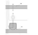
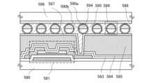
本実施の形態のボトムゲート構造の薄膜トランジスタを図1に示す。図1(A)は断面図
であり、図1(B)は平面図である。図1(A)は、図1(B)における線A1-A2の
断面図となっている。FIG. 1 shows a bottom-gate structure thin film transistor of this embodiment. FIG. 1(A) is a cross-sectional view, and FIG. 1(B) is a plan view. FIG. 1(A) is a cross-sectional view taken along line A1-A2 in FIG. 1(B).
図1に示す薄膜トランジスタには、基板100上にゲート電極層101が設けられ、ゲー
ト電極層101上にゲート絶縁層102が設けられ、ゲート絶縁層102上に酸化物半導
体層106が設けられ、酸化物半導体層106上に絶縁性酸化物を含む酸化物半導体層1
03が設けられ、絶縁性酸化物を含む酸化物半導体層103上にソース電極層又はドレイ
ン電極層105a、105bが設けられている。In the thin film transistor shown in FIG. 1, a
03 is provided, and source or drain
ゲート電極層101は、アルミニウム、銅、モリブデン、チタン、クロム、タンタル、タ
ングステン、ネオジム、スカンジウムなどの金属材料、またはこれらの金属材料を主成分
とする合金材料、またはこれらの金属材料を成分とする窒化物を用いて、単層又は積層で
形成する。アルミニウムや銅などの低抵抗導電性材料で形成するのが望ましいが、耐熱性
が低い、または腐食しやすいという問題点があるので耐熱性導電性材料と組み合わせて用
いるのが好ましい。耐熱性導電性材料としては、モリブデン、チタン、クロム、タンタル
、タングステン、ネオジム、スカンジウム等を用いる。The
例えば、ゲート電極層101の積層構造としては、アルミニウム層上にモリブデン層が積
層された二層の積層構造、または銅層上にモリブデン層を積層した二層構造、または銅層
上に窒化チタン層若しくは窒化タンタル層を積層した二層構造、窒化チタン層とモリブデ
ン層とを積層した二層構造とすることが好ましい。三層の積層構造としては、タングステ
ン層または窒化タングステン層と、アルミニウムとシリコンの合金層またはアルミニウム
とチタンの合金層と、窒化チタン層またはチタン層とを積層した構造とすることが好まし
い。For example, the stacked structure of the
酸化物半導体層106としては、In-Ga-Zn-O系、In-Sn-Zn-O系、G
a-Sn-Zn-O系、In-Zn-O系、Sn-Zn-O系、In-Sn-O系、Ga
-Zn-O系、In-O系、Sn-O系またはZn-O系の酸化物半導体からなる非単結
晶膜が好ましい。The
a-Sn-Zn-O system, In-Zn-O system, Sn-Zn-O system, In-Sn-O system, Ga
A non-single crystal film made of a -Zn-O-based, In-O-based, Sn-O-based, or Zn-O-based oxide semiconductor is preferred.
本明細書中で、In-Ga-Zn-O系の酸化物半導体とは、少なくともIn、Ga及び
Znを含む酸化物半導体のことである。また、In-Sn-Zn-O系の酸化物半導体と
は、少なくともIn、Sn及びZnを含む酸化物半導体のことである。また、Ga-Sn
-Zn-O系の酸化物半導体とは、少なくともGa、Sn及びZnを含む酸化物半導体の
ことである。また、In-Zn-O系の酸化物半導体とは、少なくともIn及びZnを含
む酸化物半導体のことである。また、Sn-Zn-O系の酸化物半導体とは、少なくとも
Sn及びZnを含む酸化物半導体のことである。また、In-Sn-O系の酸化物半導体
とは、少なくともIn及びSnを含む酸化物半導体のことである。また、Ga-Zn-O
系の酸化物半導体とは、少なくともGa及びZnを含む酸化物半導体のことである。また
、In-O系の酸化物半導体とは、少なくともInを含む酸化物半導体のことである。ま
た、Sn-O系の酸化物半導体とは、少なくともSnを含む酸化物半導体のことである。
また、Zn-O系の酸化物半導体とは、少なくともZnを含む酸化物半導体のことである
。また、上記酸化物半導体中には、Fe、Ni、Mn又はCoから選ばれた一又は複数の
金属元素が含まれていてもよい。In this specification, an In-Ga-Zn-O-based oxide semiconductor is an oxide semiconductor containing at least In, Ga, and Zn. Further, an In-Sn-Zn-O-based oxide semiconductor is an oxide semiconductor containing at least In, Sn, and Zn. Also, Ga-Sn
The -Zn-O-based oxide semiconductor is an oxide semiconductor containing at least Ga, Sn, and Zn. Further, an In-Zn-O-based oxide semiconductor is an oxide semiconductor containing at least In and Zn. Further, the Sn-Zn-O-based oxide semiconductor is an oxide semiconductor containing at least Sn and Zn. Further, an In-Sn-O-based oxide semiconductor is an oxide semiconductor containing at least In and Sn. Also, Ga-Zn-O
The term "based oxide semiconductor" refers to an oxide semiconductor containing at least Ga and Zn. Furthermore, an In—O-based oxide semiconductor refers to an oxide semiconductor containing at least In. Further, the Sn—O-based oxide semiconductor refers to an oxide semiconductor containing at least Sn.
Further, a Zn—O-based oxide semiconductor refers to an oxide semiconductor containing at least Zn. Further, the oxide semiconductor may contain one or more metal elements selected from Fe, Ni, Mn, or Co.
また、酸化物半導体層106は、必ずしも非晶質(アモルファス)構造である必要はなく
、内部に結晶粒(ナノクリスタル)を含む場合もある。結晶粒(ナノクリスタル)は直径
1nm~10nm、代表的には2nm~4nm程度である。なお、結晶状態は、X線回折
(XRD:X-ray diffraction)の分析により評価するものとする。Further, the
酸化物半導体層106の膜厚は、10nm~300nmとし、好ましくは20nm~10
0nmとする。The thickness of the
It is set to 0 nm.
絶縁性酸化物を含む酸化物半導体層103としては、In-Ga-Zn-O系、In-S
n-Zn-O系、Ga-Sn-Zn-O系、In-Zn-O系、Sn-Zn-O系、In
-Sn-O系、Ga-Zn-O系、In-O系、Sn-O系またはZn-O系の酸化物半
導体からなる非単結晶膜に絶縁性酸化物を含ませたものが好ましい。ここで、絶縁性酸化
物としては、酸化シリコンが好ましい。また、絶縁性酸化物には窒素を加えてもよい。As the
n-Zn-O series, Ga-Sn-Zn-O series, In-Zn-O series, Sn-Zn-O series, In
A non-single crystal film made of a -Sn-O, Ga-Zn-O, In-O, Sn-O, or Zn-O-based oxide semiconductor containing an insulating oxide is preferable. Here, silicon oxide is preferable as the insulating oxide. Further, nitrogen may be added to the insulating oxide.
また、絶縁性酸化物を含む酸化物半導体層103は、非晶質(アモルファス)構造である
。なお、酸化物半導体層106と同様に結晶状態は、X線回折(XRD:X-ray d
iffraction)の分析により評価するものとする。Further, the
The evaluation shall be made by analyzing the iffraction.
さらに、絶縁性酸化物を含む酸化物半導体層103はスパッタ法で形成し、ターゲットと
して、SiO2を0.1重量パーセント以上30重量パーセント以下、好ましくは1重量
パーセント以上10重量パーセント以下含ませたものを用いるのが好ましい。Further, the
絶縁性酸化物を含む酸化物半導体層103に酸化シリコンのような絶縁性酸化物を含ませ
ることにより、該絶縁性酸化物を含む酸化物半導体層103の結晶化を抑制し、非晶質構
造とすることができる。絶縁性酸化物を含む酸化物半導体層103の結晶化を抑制し、非
晶質構造とすることにより、薄膜トランジスタの特性のばらつきを低減し、安定化するこ
とが可能となる。また、300℃乃至600℃の熱処理を行っても、絶縁性酸化物を含む
酸化物半導体層103の結晶化又は微結晶粒の生成を防ぐことができる。By including an insulating oxide such as silicon oxide in the
絶縁性酸化物を含む酸化物半導体層103は、非晶質構造をとっており、内部に結晶又は
結晶粒を含まないので、導電性が低減されている。よって、酸化物半導体層106と、ソ
ース電極層又はドレイン電極層105a、105bとの間に、非晶質構造をとる絶縁性酸
化物を含む酸化物半導体層103を介することによって薄膜トランジスタのしきい値電圧
のばらつきを低減し、電気特性を安定させることができる。また、オフ電流を低減するこ
ともできる。The
絶縁性酸化物を含む酸化物半導体層103の膜厚は、10nm~300nmとし、好まし
くは20nm~100nmとする。また、絶縁性酸化物を含む酸化物半導体層103は、
ソース電極層又はドレイン電極層105a、105bの間に、ソース電極層又はドレイン
電極層105a、105bと重なる領域よりも膜厚の薄い領域を有してもよい。The thickness of the
There may be a region between the source or drain
ソース電極層又はドレイン電極層105a、105bは、アルミニウム、銅、モリブデン
、チタン、クロム、タンタル、タングステン、ネオジム、スカンジウムなどの金属材料、
またはこれらの金属材料を主成分とする合金材料、またはこれらの金属材料を成分とする
窒化物を用いることができる。アルミニウムや銅などの低抵抗導電性材料で形成するのが
望ましいが、耐熱性が低い、または腐食しやすいという問題点があるので耐熱性導電性材
料と組み合わせて用いるのが好ましい。耐熱性導電性材料としては、モリブデン、チタン
、クロム、タンタル、タングステン、ネオジム、スカンジウム等を用いる。The source electrode layer or
Alternatively, an alloy material containing these metal materials as a main component or a nitride containing these metal materials as a component can be used. It is preferable to use a low-resistance conductive material such as aluminum or copper, but since it has the problem of low heat resistance or easy corrosion, it is preferable to use it in combination with a heat-resistant conductive material. As the heat-resistant conductive material, molybdenum, titanium, chromium, tantalum, tungsten, neodymium, scandium, etc. are used.
例えば、第1の導電層及び第3の導電層に耐熱性導電性材料であるチタンを用い、第2の
導電層に低抵抗であるネオジムを含むアルミニウム合金を用いる、3層構造とするのが好
ましい。このような構成にすることで、アルミニウムの低抵抗性を活かしつつ、ヒロック
の発生を低減することができる。なお、これに限られることはなく、単層構造としてもよ
いし、2層構造としてもよいし、4層以上の構造としてもよい。For example, a three-layer structure in which titanium, which is a heat-resistant conductive material, is used for the first conductive layer and the third conductive layer, and an aluminum alloy containing neodymium, which has low resistance, is used for the second conductive layer. preferable. With such a configuration, it is possible to reduce the occurrence of hillocks while taking advantage of the low resistance of aluminum. Note that the structure is not limited to this, and may be a single layer structure, a two layer structure, or a four or more layer structure.
次に、酸化物半導体層106の上に絶縁性酸化物を含む酸化物半導体層103を積層した
薄膜トランジスタの効果について、計算機シミュレーションの結果を基に説明する。ここ
では、バックチャネルに発生するキャリアによる、薄膜トランジスタのしきい値電圧の変
化について検証を行う。なお本明細書中で、バックチャネルとは、薄膜トランジスタの活
性層における、ソース電極層又はドレイン電極層と重なっていない部分で、ゲート電極層
及びゲート絶縁層とは逆側の部分のことである。Next, the effect of a thin film transistor in which the
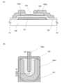
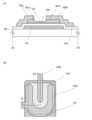
図36(A)乃至図36(C)に計算モデルとして用いた薄膜トランジスタの構造を示す
。各薄膜トランジスタは、ゲート電極層601と、ゲート電極層601の上に設けられた
ゲート絶縁層602と、ゲート絶縁層602の上に設けられた、酸化物半導体からなる活
性層と、活性層の上に設けられたソース電極層又はドレイン電極層605a、605bに
よって構成される。各薄膜トランジスタのチャネル長は10μm、チャネル幅は100μ
mとした。ゲート電極層601は、膜厚100nmのタングステンを想定し、仕事関数を
4.6eVと仮定した。また、ゲート絶縁層602は、膜厚100nmの酸化窒化シリコ
ンを想定し、誘電率を4.1と仮定した。また、ソース電極層又はドレイン電極層605
a、605bは、膜厚100nmのチタンを想定し、仕事関数を4.3eVと仮定した。FIGS. 36A to 36C show the structure of a thin film transistor used as a calculation model. Each thin film transistor includes a
It was set as m. The
a and 605b are assumed to be titanium with a film thickness of 100 nm, and the work function is assumed to be 4.3 eV.
ここで、酸化物半導体は、酸素欠損や水素の侵入によって、余剰なキャリアを形成するこ
とが知られている。薄膜トランジスタのバックチャネルは、ソース電極層又はドレイン電
極層605a、605bをエッチングする際のプラズマダメージにより、酸素欠損が生じ
やすく、余剰なキャリアが発生しやすい。また、大気中や層間膜からの水素の侵入によっ
て、バックチャネルに余剰なキャリアが発生することもあり得る。よって、各薄膜トラン
ジスタのバックチャネルに、エッチングや成膜などの工程による酸素欠損や水素の侵入に
より発生したキャリア(電子)を設定した。Here, it is known that an oxide semiconductor forms surplus carriers due to oxygen vacancies and hydrogen intrusion. In the back channel of a thin film transistor, oxygen vacancies are likely to occur due to plasma damage during etching of the source electrode layer or
図36(A)に示す構造Aの薄膜トランジスタは、単層の酸化物半導体層606からなる
活性層を有する。酸化物半導体層606は、膜厚50nmのIn-Ga-Zn-O系非単
結晶膜を想定し、電子真性移動度は20cm2/Vs、バンドギャップ(Eg)は3.0
5eV、電子親和力(χ)は4.3eVと仮定した。A thin film transistor with structure A illustrated in FIG. 36A has an active layer made of a single-layer
5 eV, and the electron affinity (χ) was assumed to be 4.3 eV.
図36(B)に示す構造Bの薄膜トランジスタは、酸化物半導体層616と酸化物半導体
層616上に形成された絶縁性酸化物を含む酸化物半導体層613の積層構造の活性層を
有する。絶縁性酸化物を含む酸化物半導体層613は、膜厚25nmの、酸化シリコンを
含むIn-Ga-Zn-O系非単結晶膜を想定し、電子真性移動度は2cm2/Vsと仮
定した。酸化シリコンを含むことによって、In-Ga-Zn-O系非単結晶膜の電子真
性移動度は低下するものとする。酸化物半導体層616は、膜厚25nmのIn-Ga-
Zn-O系非単結晶膜を想定し、電子真性移動度は20cm2/Vsと仮定した。絶縁性
酸化物を含む酸化物半導体層613及び酸化物半導体層616ともに、バンドギャップ(
Eg)は3.05eV、電子親和力(χ)は4.3eV、と仮定した。A thin film transistor with structure B illustrated in FIG. 36B has an active layer with a stacked-layer structure of an
A Zn-O based non-single crystal film was assumed, and the electron intrinsic mobility was assumed to be 20 cm2 /Vs. Both the
Eg) was assumed to be 3.05 eV, and electron affinity (χ) was assumed to be 4.3 eV.
図36(C)に示す構造Cの薄膜トランジスタは、酸化物半導体層626と酸化物半導体
層626上に形成された絶縁性酸化物を含む酸化物半導体層623の積層構造の活性層を
有する。ただし、構造Cの絶縁性酸化物を含む酸化物半導体層623は、構造Bの絶縁性
酸化物を含む酸化物半導体層613より、多くの酸化シリコンを含有する。絶縁性酸化物
を含む酸化物半導体層623は、膜厚25nmの、酸化シリコンを含むIn-Ga-Zn
-O系非単結晶膜を想定し、電子真性移動度は0.2cm2/Vsと仮定した。構造Bよ
り多くの酸化シリコンを含むことによって、In-Ga-Zn-O系非単結晶膜の電子真
性移動度は構造Bより低下するものとする。酸化物半導体層626は、膜厚25nmのI
n-Ga-Zn-O系非単結晶膜を想定し、電子真性移動度は20cm2/Vsと仮定し
た。絶縁性酸化物を含む酸化物半導体層623及び酸化物半導体層626ともに、バンド
ギャップ(Eg)は3.05eV、電子親和力(χ)は4.3eV、と仮定した。A thin film transistor with structure C illustrated in FIG. 36C has an active layer with a stacked-layer structure of an
A --O-based non-single crystal film was assumed, and the electron intrinsic mobility was assumed to be 0.2 cm2 /Vs. It is assumed that the electron intrinsic mobility of the In--Ga--Zn--O-based non-single crystal film is lower than that of structure B because it contains more silicon oxide than structure B. The
An n-Ga-Zn-O non-single crystal film was assumed, and the electron intrinsic mobility was assumed to be 20 cm2 /Vs. It was assumed that both the
上記の各薄膜トランジスタのバックチャネルの表面から5nmの深さに、エッチングや成
膜などの工程による酸素欠損や水素の侵入により発生したキャリア(電子)をキャリア密
度5×1016cm―3、1×1017cm―3、2.5×1017cm―3、5×10
17cm―3、1×1018cm―3で設定し、各キャリア密度におけるしきい値電圧を
計算機シミュレーションにより算出した。At a depth of 5 nm from the surface of the back channel of each of the above thin film transistors, carriers (electrons) generated due to oxygen vacancies and hydrogen intrusion during processes such as etching and film formation are placed at a carrier density of 5×1016 cm−3 , 1× 1017 cm-3 , 2.5 x 1017 cm-3 , 5 x 10
17 cm−3 and 1×1018 cm−3 , and the threshold voltage at each carrier density was calculated by computer simulation.
なお、上記のモデルの計算には、Silvaco Data Systems Inc.
製のデバイスシミュレーションソフト「Atlas」を用いた。オフ電流の計算について
は、バンド間トンネリングモデルを使用した。Note that the calculation of the above model was performed using Silvaco Data Systems Inc.
We used the device simulation software "Atlas" manufactured by Manufacturer. For calculation of off-state current, an interband tunneling model was used.
図36(A)乃至図36(C)に示す各構造の薄膜トランジスタのしきい値電圧の、バッ
クチャネルのキャリア密度依存性を図37に示す。図37において、縦軸は各構造の薄膜
トランジスタのしきい値電圧(Vth[V])を示し、横軸は、各構造の活性層のバック
チャネルに発生するキャリアの濃度(cm―3)を示している。FIG. 37 shows the dependence of the threshold voltage of the thin film transistors having the respective structures shown in FIGS. 36(A) to 36(C) on the back channel carrier density. In FIG. 37, the vertical axis indicates the threshold voltage (Vth [V]) of the thin film transistor of each structure, and the horizontal axis indicates the concentration of carriers generated in the back channel of the active layer of each structure (cm-3 ). ing.
本計算では、薄膜トランジスタのしきい値電圧(Vth[V])を、ゲート電圧(Vg[
V])を横軸、ドレイン電流の平方根(Id1/2)を縦軸にプロットしたグラフにおい
て、Id1/2の傾きが最大となる接線とVg軸との接点で定義する。In this calculation, the threshold voltage (Vth[V]) of the thin film transistor is defined as the gate voltage (Vg[V]
In a graph in which V]) is plotted on the horizontal axis and the square root of the drain current (Id1/2 ) is plotted on the vertical axis, it is defined as the point of contact between the tangent line with the maximum slope of Id1/2 and the Vg axis.
図37に示すように、構造Aの薄膜トランジスタは、バックチャネルのキャリア密度が増
加するにつれて、しきい値電圧の絶対値も増加している。バックチャネルのキャリア密度
5×1016cm―3~1×1018cm―3に対して、構造Aのしきい値電圧は3V近
くシフトしている。As shown in FIG. 37, in the thin film transistor of structure A, as the back channel carrier density increases, the absolute value of the threshold voltage also increases. For a back channel carrier density of 5×1016 cm−3 to 1×1018 cm−3 , the threshold voltage of structure A is shifted by nearly 3 V.
構造Aと比較すると、活性層が酸化物半導体層616と絶縁性酸化物を含む酸化物半導体
層613との積層構造である構造Bは、バックチャネルのキャリア密度に対するしきい値
電圧の絶対値の増加が小さくなっている。バックチャネルのキャリア密度5×10¹⁶c
m―3~1×1018cm―3に対して、構造Bのしきい値電圧は1V以下しかシフトし
ていない。Compared to structure A, structure B, in which the active layer has a stacked structure of an
m−3 to 1×1018 cm−3 , the threshold voltage of structure B shifts by less than 1 V.
構造Bより、絶縁性酸化物を含む酸化物半導体層623が多くの酸化シリコンを含む構造
Cは、バックチャネルのキャリア密度に対するしきい値電圧の絶対値の増加が、構造Bよ
りさらに小さくなっている。バックチャネルのキャリア密度5×1016cm―3~1×
1018cm―3に対して、構造Cのしきい値電圧は0.5V程度しかシフトしていない
。Compared to structure B, in structure C in which the
1018 cm−3 , the threshold voltage of structure C shifts by only about 0.5 V.
また、図36(A)乃至図36(C)に示す各構造の薄膜トランジスタの飽和移動度の、
バックチャネルのキャリア密度依存性を図38に示す。縦軸は各構造の薄膜トランジスタ
の飽和移動度(μFE(sat)[cm2/Vs])を示し、横軸は、図37と同様であ
る。In addition, the saturation mobility of the thin film transistor of each structure shown in FIGS. 36(A) to 36(C) is
FIG. 38 shows the carrier density dependence of the back channel. The vertical axis indicates the saturation mobility (μFE (sat) [cm2 /Vs]) of the thin film transistor of each structure, and the horizontal axis is the same as in FIG. 37.
図38より、構造B、構造Cの薄膜トランジスタは、構造Aのトランジスタとほぼ同程度
の飽和移動度を有していることが分かる。よって、電子真性移動度の低い絶縁性酸化物を
含む酸化物半導体層を積層して、バックチャネルのキャリアによるしきい値電圧の変化を
低減しても、薄膜トランジスタの飽和移動度及びオン電流を維持することができる。From FIG. 38, it can be seen that the thin film transistors of structure B and structure C have saturation mobilities that are approximately the same as the transistor of structure A. Therefore, even if oxide semiconductor layers containing insulating oxides with low intrinsic electron mobility are stacked to reduce changes in threshold voltage due to carriers in the back channel, the saturation mobility and on-current of the thin film transistor can be maintained. can do.
以上より、薄膜トランジスタの活性層を、絶縁性酸化物を含む酸化物半導体層と酸化物半
導体層との積層構造にすることによって、薄膜トランジスタの飽和移動度を下げることな
く、バックチャネルのキャリアによるしきい値電圧の変化を低減できることが示された。
よって、絶縁性酸化物を含む酸化物半導体層と酸化物半導体層との積層した活性層を有す
る薄膜トランジスタを画像表示装置の画素部に用いることで、スイッチングトランジスタ
のしきい値電圧のばらつきを低減し、各画素間の輝度のばらつきを低減することができる
。From the above, by forming the active layer of a thin film transistor into a stacked structure of an oxide semiconductor layer containing an insulating oxide and an oxide semiconductor layer, it is possible to reduce the threshold by carriers in the back channel without lowering the saturation mobility of the thin film transistor. It has been shown that the change in value voltage can be reduced.
Therefore, by using a thin film transistor having an active layer in which an oxide semiconductor layer containing an insulating oxide and an oxide semiconductor layer are stacked in the pixel portion of an image display device, variations in the threshold voltage of the switching transistor can be reduced. , it is possible to reduce variations in brightness between pixels.
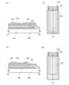
また、図1(A)及び図1(B)に示す逆スタガ型構造の薄膜トランジスタに限られず、
図12(A)及び図12(B)に示すように、絶縁性酸化物を含む酸化物半導体層103
の上にチャネル保護層104が設けられた逆スタガ型構造の薄膜トランジスタとしてもよ
い。なお、図12(A)は、図12(B)における線A1-A2の断面図である。チャネ
ル保護層104としては、プラズマCVD法や熱CVD法などの気相成長法やスパッタリ
ング法で成膜された無機材料(酸化珪素、窒化珪素、酸化窒化珪素、窒化酸化珪素など)
を用いることができる。絶縁性酸化物を含む酸化物半導体層103の上にチャネル保護層
104を設ける構造とすることによって、絶縁性酸化物を含む酸化物半導体層103のチ
ャネル形成領域に対する製作工程におけるダメージ(絶縁性酸化物を含む酸化物半導体層
103形成におけるエッチングのプラズマや、エッチング剤による膜減りや、酸化など)
を防ぐことができる。よって、薄膜トランジスタの信頼性を向上させることができる。な
お、図12(A)及び図12(B)に示す薄膜トランジスタは、絶縁性酸化物を含む酸化
物半導体層103の上に形成されているチャネル保護層104以外は、図1に示す薄膜ト
ランジスタと同じ構造をとっており、図面の符号も図1に示す薄膜トランジスタと同一の
ものを用いている。Furthermore, the present invention is not limited to the thin film transistor having an inverted staggered structure shown in FIGS. 1(A) and 1(B),
As shown in FIGS. 12A and 12B, an
A thin film transistor having an inverted staggered structure in which a channel
can be used. By providing a structure in which the channel
can be prevented. Therefore, the reliability of the thin film transistor can be improved. Note that the thin film transistors shown in FIGS. 12(A) and 12(B) are the same as the thin film transistor shown in FIG. 1 except for the channel
また、図1(A)及び図1(B)に示す逆スタガ構造の薄膜トランジスタでは、ゲート電
極層101のチャネル方向の幅が、絶縁性酸化物を含む酸化物半導体層103及び酸化物
半導体層106のチャネル方向の幅よりも広い構造となっているが、本実施の形態に示す
薄膜トランジスタはこれに限られるものではない。図30(A)及び図30(B)に示す
ように、絶縁性酸化物を含む酸化物半導体層103及び酸化物半導体層106のチャネル
方向の幅より、ゲート電極層のチャネル方向の幅が狭いゲート電極層201を用いてもよ
い。なお、図30(A)は、図30(B)における線A1-A2の断面図である。このよ
うな構造をとることによって、ゲート電極層201と、ソース電極層又はドレイン電極層
105a、105bとの距離が広がるので、ソース電極層又はドレイン電極層105a、
105bから酸化物半導体層106に直接流れるオフ電流を低減することができる。よっ
て薄膜トランジスタの信頼性向上を図ることができる。なお、図30(A)及び図30(
B)に示す薄膜トランジスタは、ゲート電極層201を除き、図1(A)及び図1(B)
に示す薄膜トランジスタと対応する部位に関して図面の符号も図1(A)及び図1(B)
に示す薄膜トランジスタと同一のものを用いている。In addition, in the inverted staggered thin film transistor shown in FIGS. 1A and 1B, the width of the
Off-state current flowing directly from the
The thin film transistor shown in FIG. 1(A) and FIG. 1(B) except for the
The reference numerals in the drawings for parts corresponding to the thin film transistors shown in FIG. 1(A) and FIG. 1(B)
The same thin film transistor as shown in is used.
また、図1(A)及び図1(B)に示す逆スタガ型構造の薄膜トランジスタでは、酸化物
半導体層106と、ソース電極層又はドレイン電極層105a、105bとが、酸化物半
導体層106の端部において直接接触しているが、本実施の形態に示す薄膜トランジスタ
はこれに限られるものではない。図31(A)及び図31(B)に示すように、絶縁性酸
化物を含む酸化物半導体層103に対して酸化物半導体層106の面積が小さく、絶縁性
酸化物を含む酸化物半導体層103の端部の下に空洞210が形成されるような構造とし
てもよい。空洞210は、酸化物半導体層106、絶縁性酸化物を含む酸化物半導体層1
03、ソース電極層又はドレイン電極層105a、105b及びゲート絶縁層102に囲
まれるように形成される。なお、酸化物半導体層106上にソース電極層又はドレイン電
極層105a、105bが設けられていない部分では、ソース電極層又はドレイン電極層
105a、105bの代わりに薄膜トランジスタ上の保護絶縁層が空洞210を形成する
。空洞210は、酸化物半導体層106より絶縁性酸化物を含む酸化物半導体層103の
方がウェットエッチングに対するエッチングレートが小さいことを利用して容易に形成す
ることができる。このような構造をとることによって、酸化物半導体層106と、ソース
電極層又はドレイン電極層105a、105bとが直接接触することがなくなるので、ソ
ース電極層又はドレイン電極層105a、105bから酸化物半導体層106の端部に直
接流れるオフ電流を低減することができる。よって、薄膜トランジスタの信頼性向上を図
ることができる。なお、図31(A)及び図31(B)に示す薄膜トランジスタは、絶縁
性酸化物を含む酸化物半導体層103の端部の下に空洞210が形成されていること以外
は、図1に示す薄膜トランジスタと同じ構造をとっており、図面の符号も図1に示す薄膜
トランジスタと同一のものを用いている。In addition, in the thin film transistor with the inverted staggered structure shown in FIGS. Although the thin film transistor shown in this embodiment is not limited to this, the thin film transistor is in direct contact at some portions. As shown in FIGS. 31A and 31B, the area of the
03, it is formed so as to be surrounded by the source or drain
また、図32(A)及び図32(B)に示すように、酸化物半導体層226の端部が絶縁
性酸化物を含む酸化物半導体層223によって覆われるような構造としてもよい。なお、
図32(A)は、図32(B)における線A1-A2の断面図である。このような構造を
とることによって、酸化物半導体層226と、ソース電極層又はドレイン電極層105a
、105bとが直接接触することがなくなるので、ソース電極層又はドレイン電極層10
5a、105bから酸化物半導体層226の端部に直接流れるオフ電流を低減することが
できる。よって、薄膜トランジスタの信頼性向上を図ることができる。なお、図32(A
)及び図32(B)に示す薄膜トランジスタは、酸化物半導体層226の端部が絶縁性酸
化物を含む酸化物半導体層223によって覆われていること以外は、図1に示す薄膜トラ
ンジスタと同じ構造をとっており、図面の符号も図1に示す薄膜トランジスタと同一のも
のを用いている。Alternatively, as shown in FIGS. 32A and 32B, an end portion of the
FIG. 32(A) is a cross-sectional view taken along line A1-A2 in FIG. 32(B). By adopting such a structure, the
, 105b, the source electrode layer or drain electrode layer 10
Off-state current flowing directly from 5a and 105b to the end of the
) and FIG. 32B have the same structure as the thin film transistor shown in FIG. 1, except that the end portions of the
また、図1(A)及び図1(B)に示す逆スタガ構造の薄膜トランジスタでは、ソース電
極層又はドレイン電極層105a、105bの間に絶縁性酸化物を含む酸化物半導体層1
03が形成され、酸化物半導体層106が覆われているが、本実施の形態に示す薄膜トラ
ンジスタはこれに限られるものではない。図33(A)及び図33(B)に示すように、
ソース電極層又はドレイン電極層105a、105bの間の絶縁性酸化物を含む酸化物半
導体層をエッチングして絶縁性酸化物を含む酸化物半導体層233a、233bを形成し
、酸化物半導体層106が露出されるような構造としてもよい。なお、図33(A)は、
図33(B)における線A1-A2の断面図である。また、酸化物半導体層106は、絶
縁性酸化物を含む酸化物半導体層233a、233bの間に、絶縁性酸化物を含む酸化物
半導体層233a、233bと重なる領域よりも膜厚の薄い領域を有していてもよい。こ
のような構造をとることによって、絶縁性酸化物を含む酸化物半導体層233a、233
bより、一般的に導電性が高い酸化物半導体層106のみにチャネル形成領域を形成する
ことができるので、絶縁性酸化物を含む酸化物半導体層233a、233bによるオフ電
流の低減に加えて、S値(サブスレッショルド係数)の改善を図ることができる。よって
、薄膜トランジスタの信頼性向上を図ることができる。なお、図33(A)及び図33(
B)に示す薄膜トランジスタは、絶縁性酸化物を含む酸化物半導体層233a、233b
がソース電極側とドレイン電極側に分離されていること以外は、図1に示す薄膜トランジ
スタと同じ構造をとっており、図面の符号も図1に示す薄膜トランジスタと同一のものを
用いている。Further, in the thin film transistor with an inverted staggered structure shown in FIGS. 1A and 1B, an
03 is formed to cover the
The oxide semiconductor layer containing an insulating oxide between the source or drain
FIG. 33B is a cross-sectional view taken along line A1-A2 in FIG. 33(B). In addition, the
b. Since the channel formation region can be formed only in the
The thin film transistor shown in B) includes
It has the same structure as the thin film transistor shown in FIG. 1, except that it is separated into a source electrode side and a drain electrode side, and the same reference numerals as in the thin film transistor shown in FIG. 1 are used in the drawings.
以上のような構成とすることで、酸化物半導体層の上に絶縁性酸化物を含む酸化物半導体
層を積層し、酸化物半導体層とソース電極層又はドレイン電極層とが絶縁性酸化物を含む
酸化物半導体層を介して接触するように薄膜トランジスタを形成し、該薄膜トランジスタ
のしきい値電圧のばらつきを低減し、電気特性を安定させることができる。また、オフ電
流を低減することもできる。With the above structure, the oxide semiconductor layer containing an insulating oxide is stacked on the oxide semiconductor layer, and the oxide semiconductor layer and the source electrode layer or the drain electrode layer contain the insulating oxide. A thin film transistor can be formed so as to be in contact with each other through the oxide semiconductor layer, and variations in threshold voltage of the thin film transistor can be reduced and electrical characteristics can be stabilized. Further, off-state current can also be reduced.
なお、本実施の形態に示す構成は、他の実施の形態に示した構成を適宜組み合わせて用い
ることができることとする。また、本実施の形態で示した構成同士を適宜組み合わせて用
いることができることとする。Note that the structure shown in this embodiment can be used in appropriate combination with the structures shown in other embodiments. Further, the structures shown in this embodiment can be used in combination as appropriate.
(実施の形態2)
本実施の形態では、実施の形態1で示した薄膜トランジスタを含む表示装置の作製工程に
ついて、図2乃至図9を用いて説明する。図2と図3は断面図で、図4乃至図7は平面図
となっており、図4乃至図7、図9に示す線A1-A2及び線B1-B2は、図2及び図
3の断面図A1-A2、B1-B2に対応している。(Embodiment 2)
In this embodiment, a manufacturing process of a display device including the thin film transistor described in
まず、基板100を準備する。基板100は、バリウムホウケイ酸ガラス、アルミノホウ
ケイ酸ガラス、若しくはアルミノシリケートガラスなど、フュージョン法やフロート法で
作製される無アルカリガラス基板、セラミック基板の他、本作製工程の処理温度に耐えう
る耐熱性を有するプラスチック基板等を用いることができる。また、ステンレス合金など
の金属基板の表面に絶縁膜を設けた基板を適用しても良い。基板100の大きさは、32
0mm×400mm、370mm×470mm、550mm×650mm、600mm×
720mm、680mm×880mm、730mm×920mm、1000mm×120
0mm、1100mm×1250mm、1150mm×1300mm、1500mm×1
800mm、1900mm×2200mm、2160mm×2460mm、2400mm
×2800mm、又は2850mm×3050mm等を用いることができる。First, a
0mm x 400mm, 370mm x 470mm, 550mm x 650mm, 600mm x
720mm, 680mm x 880mm, 730mm x 920mm, 1000mm x 120
0mm, 1100mm x 1250mm, 1150mm x 1300mm, 1500mm x 1
800mm, 1900mm x 2200mm, 2160mm x 2460mm, 2400mm
x 2800 mm, 2850 mm x 3050 mm, etc. can be used.
また基板100上に下地膜として絶縁膜を形成してもよい。下地膜としては、CVD法や
スパッタ法等を用いて、酸化シリコン膜、窒化シリコン膜、酸化窒化シリコン膜、または
窒化酸化シリコン膜を単層または積層で形成すればよい。基板100としてガラス基板の
ような可動イオンを含有する基板を用いる場合、下地膜として窒化シリコン膜、窒化酸化
シリコン膜などの窒素を含有する膜を用いることで、可動イオンが酸化物半導体層に侵入
することを防ぐことができる。Further, an insulating film may be formed on the
次に、ゲート電極層101を含むゲート配線、容量配線108、及び第1の端子121を
形成するための導電膜をスパッタ法や真空蒸着法で基板100全面に成膜する。次いで、
フォトリソグラフィ工程を行い、レジストマスクを形成し、エッチングにより不要な部分
を除去して配線及び電極(ゲート電極層101を含むゲート配線、容量配線108、及び
第1の端子121)を形成する。このとき段切れ防止のために、少なくともゲート電極層
101の端部にテーパー形状が形成されるようにエッチングするのが好ましい。この段階
での断面図を図2(A)に示した。なお、この段階での平面図が図4に相当する。Next, a conductive film for forming the gate wiring including the
A photolithography process is performed to form a resist mask, and unnecessary portions are removed by etching to form wiring and electrodes (gate wiring including
ゲート電極層101を含むゲート配線と容量配線108、端子部の第1の端子121は、
実施の形態1で示した導電性材料を用いて単層又は積層で形成することができる。The gate wiring including the
The conductive material described in
ここで、ゲート電極層101のチャネル方向の幅が、後の工程で作製する絶縁性酸化物を
含む酸化物半導体層103及び酸化物半導体層106のチャネル方向の幅より狭くなるよ
うにゲート電極層101を形成してもよい。このようにゲート電極層101を形成するこ
とによって、図30(A)及び図30(B)に示すような薄膜トランジスタを形成するこ
とができる。図30に示すような薄膜トランジスタでは、ゲート電極層201と、ソース
電極層又はドレイン電極層105a、105bとの距離が広がるので、ソース電極層又は
ドレイン電極層105a、105bから酸化物半導体層106に直接流れるオフ電流を低
減することができる。Here, the width of the
次いで、ゲート電極層101上にゲート絶縁層102を全面に成膜する。ゲート絶縁層1
02はCVD法やスパッタ法などを用い、膜厚を50~250nmとする。Next, a
02 uses a CVD method, a sputtering method, etc., and has a film thickness of 50 to 250 nm.
例えば、ゲート絶縁層102としてCVD法やスパッタ法により酸化シリコン膜を用い、
100nmの厚さで形成する。勿論、ゲート絶縁層102はこのような酸化シリコン膜に
限定されるものでなく、酸化窒化シリコン膜、窒化酸化シリコン膜、窒化シリコン膜、酸
化アルミニウム膜、酸化タンタル膜などの他の絶縁膜を用い、これらの材料から成る単層
または積層構造として形成しても良い。For example, a silicon oxide film is used as the
It is formed to have a thickness of 100 nm. Of course, the
また、ゲート絶縁層102として、有機シランガスを用いたCVD法により酸化シリコン
層を形成することも可能である。有機シランガスとしては、珪酸エチル(TEOS:化学
式Si(OC2H5)4)、テトラメチルシラン(TMS:化学式Si(CH3)4)、
テトラメチルシクロテトラシロキサン(TMCTS)、オクタメチルシクロテトラシロキ
サン(OMCTS)、ヘキサメチルジシラザン(HMDS)、トリエトキシシラン(Si
H(OC2H5)3)、トリスジメチルアミノシラン(SiH(N(CH3)2)3)等
のシリコン含有化合物を用いることができる。Furthermore, it is also possible to form a silicon oxide layer as the
Tetramethylcyclotetrasiloxane (TMCTS), octamethylcyclotetrasiloxane (OMCTS), hexamethyldisilazane (HMDS), triethoxysilane (Si
Silicon-containing compounds such as H(OC2 H5 )3 ) and trisdimethylaminosilane (SiH(N(CH3 )2 )3 ) can be used.
また、ゲート絶縁層102として、アルミニウム、イットリウム、又はハフニウムの酸化
物、窒化物、酸化窒化物、又は窒化酸化物の一種又はそれらの化合物を少なくとも2種以
上含む化合物を用いることもできる。Further, as the
なお、本明細書において、酸化窒化物とは、その組成として、窒素原子よりも酸素原子の
数が多い物質のことを指し、窒化酸化物とは、その組成として、酸素原子より窒素原子の
数が多い物質のことを指す。例えば、酸化窒化シリコン膜とは、その組成として、窒素原
子よりも酸素原子の数が多く、ラザフォード後方散乱法(RBS:Rutherford
Backscattering Spectrometry)及び水素前方散乱法(H
FS:Hydrogen Forward Scattering)を用いて測定した場
合に、濃度範囲として酸素が50~70原子%、窒素が0.5~15原子%、シリコンが
25~35原子%、水素が0.1~10原子%の範囲で含まれるものをいう。また、窒化
酸化シリコン膜とは、その組成として、酸素原子より窒素原子の数が多く、RBS及びH
FSを用いて測定した場合に、濃度範囲として酸素が5~30原子%、窒素が20~55
原子%、シリコンが25~35原子%、水素が10~30原子%の範囲で含まれるものを
いう。但し、酸化窒化シリコンまたは窒化酸化シリコンを構成する原子の合計を100原
子%としたとき、窒素、酸素、シリコン及び水素の含有比率が上記の範囲内に含まれるも
のとする。In this specification, oxynitride refers to a substance whose composition has more oxygen atoms than nitrogen atoms, and nitrided oxide refers to a substance whose composition has more nitrogen atoms than oxygen atoms. Refers to substances with a large amount of For example, a silicon oxynitride film has a composition in which there are more oxygen atoms than nitrogen atoms, and the composition is based on the Rutherford backscattering method (RBS).
backscattering spectrometry) and hydrogen forward scattering method (H
When measured using Hydrogen Forward Scattering (FS), the concentration range is 50 to 70 atom% for oxygen, 0.5 to 15 atom% for nitrogen, 25 to 35 atom% for silicon, and 0.1 to 10 atom% for hydrogen. This refers to substances contained within the range of atomic percent. In addition, a silicon nitride oxide film has a composition in which there are more nitrogen atoms than oxygen atoms, and RBS and H
When measured using FS, the concentration range is 5 to 30 at% for oxygen and 20 to 55 at% for nitrogen.
Silicon is contained in the range of 25 to 35 atom%, and hydrogen is contained in the range of 10 to 30 atom%. However, when the total of atoms constituting silicon oxynitride or silicon nitride oxide is 100 atomic %, the content ratios of nitrogen, oxygen, silicon, and hydrogen are included within the above range.
なお、酸化物半導体層106を形成するための酸化物半導体膜を成膜する前に、基板10
0が設置されたチャンバー内にアルゴンガスを導入してプラズマを発生させる逆スパッタ
を行い、ゲート絶縁層の表面に付着しているゴミを除去することが好ましい。また、逆ス
パッタを行うことにより、ゲート絶縁層102表面の平坦性を向上させることもできる。
逆スパッタとは、ターゲット側に電圧を印加せずに、アルゴン雰囲気下で基板側にRF電
源を用いて電圧を印加して基板にプラズマを形成して表面を改質する方法である。なお、
アルゴン雰囲気に代えて窒素、ヘリウムなどを用いてもよい。また、アルゴン雰囲気に酸
素、N2Oなどを加えた雰囲気で行ってもよい。また、アルゴン雰囲気にCl2、CF4
などを加えた雰囲気で行ってもよい。逆スパッタ処理後、大気に曝すことなく第1の酸化
物半導体膜を成膜することによって、ゲート絶縁層102と、酸化物半導体層106との
界面にゴミや水分が付着するのを防ぐことができる。Note that before forming the oxide semiconductor film for forming the
It is preferable to perform reverse sputtering in which argon gas is introduced into a chamber in which a gate insulating layer is installed to generate plasma to remove dust adhering to the surface of the gate insulating layer. Further, by performing reverse sputtering, the flatness of the surface of the
Reverse sputtering is a method in which a voltage is applied to the substrate using an RF power source in an argon atmosphere without applying a voltage to the target to form plasma on the substrate to modify the surface. In addition,
Nitrogen, helium, or the like may be used instead of the argon atmosphere. Alternatively, an atmosphere in which oxygen, N2 O, or the like is added to the argon atmosphere may be used. In addition, Cl2 and CF4 were added to the argon atmosphere.
You can also create an atmosphere with something like this. By forming the first oxide semiconductor film without exposing it to the atmosphere after reverse sputtering treatment, it is possible to prevent dust and moisture from adhering to the interface between the
次に、ゲート絶縁層102上に酸化物半導体層106を形成するための第1の酸化物半導
体膜を、スパッタ法を用いてアルゴンなどの希ガスと酸素ガスの雰囲気下で成膜する。こ
のとき、アルゴンなどの希ガスの流量の比率を酸素ガスの流量の比率より大きくして成膜
する、または、酸素ガスを用いず、アルゴンなどの希ガスのみの雰囲気下で成膜すること
によって、酸化物半導体層106の導電率を向上させることができる。第1の酸化物半導
体膜としては、実施の形態1で示した酸化物半導体を用いることができる。例えば具体的
な条件例としては、直径8インチのIn、Ga、及びZnを含む酸化物半導体ターゲット
(In2O3:Ga2O3:ZnO=1:1:1)を用いて、基板とターゲットの間との
距離を170mm、圧力0.4Pa、直流(DC)電源0.5kW、成膜ガスAr:O2
=30:15(sccm)、成膜温度を室温としてスパッタ成膜を行う。また、ターゲッ
トとしては、In2O3を含む直径8インチの円盤上にペレット状のGa2O3とZnO
を配置するようにしてもよい。なお、パルス直流(DC)電源を用いると、ごみが軽減で
き、膜厚分布も均一となるために好ましい。また、第1の酸化物半導体膜の膜厚は、10
nm~300nmとし、好ましくは20nm~100nmとする。Next, a first oxide semiconductor film for forming the
=30:15 (sccm), and sputtering film formation is performed with the film formation temperature set to room temperature. In addition, as a target, pellet-shaped Ga2 O3 and ZnO were placed on a disk with a diameter of 8 inches containing In2 O3 .
You may also place . Note that it is preferable to use a pulsed direct current (DC) power source because dust can be reduced and the film thickness distribution can be made uniform. Further, the thickness of the first oxide semiconductor film is 10
nm to 300 nm, preferably 20 nm to 100 nm.
次いで第1の酸化物半導体膜上に、大気に曝すことなく、絶縁性酸化物を含む酸化物半導
体層103を形成するための第2の酸化物半導体膜を、スパッタ法を用いてアルゴンなど
の希ガスと酸素ガスの雰囲気下で成膜する。ここで、絶縁性酸化物としては、酸化シリコ
ンが好ましい。このとき、酸素ガスの流量の比率を大きくして成膜することによって、絶
縁性酸化物を含む酸化物半導体層103の導電率を低減させることができる。第2の酸化
物半導体膜としては、実施の形態1で示した酸化物半導体を用いることができる。第2の
酸化物半導体膜を成膜する際、SiO2を0.1重量パーセント以上30重量パーセント
以下、好ましくは1重量パーセント以上10重量パーセント以下含ませた酸化物半導体タ
ーゲットを用いるのが好ましい。例えば、具体的な条件例としては、SiO2を2重量パ
ーセントの割合で含ませた直径8インチのIn、Ga、及びZnを含む酸化物半導体ター
ゲット(In2O3:Ga2O3:ZnO=1:1:1)を用いて、基板とターゲットの
間との距離を170mm、圧力0.4Pa、直流(DC)電源0.5kW、成膜ガスAr
:O2=30:15(sccm)、成膜温度を室温としてスパッタ成膜を行う。また、タ
ーゲットとしては、In2O3を含む直径8インチの円盤上にペレット状のSiO2、G
a2O3及びZnOを配置するようにしてもよい。なお、パルス直流(DC)電源を用い
ると、ごみが軽減でき、膜厚分布も均一となるために好ましい。また、第2の酸化物半導
体膜の膜厚は、10nm~300nmとし、好ましくは20nm~100nmとする。Next, a second oxide semiconductor film for forming the
:O2 =30:15 (sccm), and sputtering film formation is performed with the film formation temperature set to room temperature. In addition, asa target, pellet-shaped SiO2, G
A2 O3 and ZnO may be arranged. Note that it is preferable to use a pulsed direct current (DC) power source because dust can be reduced and the film thickness distribution can be made uniform. Further, the thickness of the second oxide semiconductor film is 10 nm to 300 nm, preferably 20 nm to 100 nm.
第2の酸化物半導体膜に酸化シリコンのような絶縁性酸化物を含ませることにより、成膜
される酸化物半導体をアモルファス化することが容易となる。また、酸化物半導体を熱処
理した場合に、結晶化してしまうのを抑制することができる。By including an insulating oxide such as silicon oxide in the second oxide semiconductor film, the formed oxide semiconductor can be easily made amorphous. Further, when the oxide semiconductor is heat-treated, crystallization can be suppressed.
第1の酸化物半導体膜及び第2の酸化物半導体膜の成膜は、先に逆スパッタを行ったチャ
ンバーと同一チャンバーを用いてもよいし、先に逆スパッタを行ったチャンバーと異なる
チャンバーで成膜してもよい。The first oxide semiconductor film and the second oxide semiconductor film may be formed in the same chamber in which the reverse sputtering was previously performed, or in a different chamber from the chamber in which the reverse sputtering was previously performed. A film may be formed.
スパッタ法にはスパッタ用電源に高周波電源を用いるRFスパッタ法と、DCスパッタ法
があり、さらにパルス的にバイアスを与えるパルスDCスパッタ法もある。RFスパッタ
法は主に絶縁膜を成膜する場合に用いられ、DCスパッタ法は主に金属膜を成膜する場合
に用いられる。Sputtering methods include an RF sputtering method that uses a high frequency power source as a sputtering power source, a DC sputtering method, and a pulsed DC sputtering method that applies a bias in a pulsed manner. The RF sputtering method is mainly used when forming an insulating film, and the DC sputtering method is mainly used when forming a metal film.
また、材料の異なるターゲットを複数設置できる多元スパッタ装置もある。多元スパッタ
装置は、同一チャンバーで異なる材料膜を積層成膜することも、同一チャンバーで複数種
類の材料を同時に放電させて成膜することもできる。There is also a multi-source sputtering device that can install multiple targets made of different materials. The multi-source sputtering apparatus can perform layered film formation of different material films in the same chamber, or can perform film formation by simultaneously discharging a plurality of types of materials in the same chamber.
また、チャンバー内部に磁石機構を備えたマグネトロンスパッタ法を用いるスパッタ装置
や、グロー放電を使わずマイクロ波を用いて発生させたプラズマを用いるECRスパッタ
法を用いるスパッタ装置がある。Furthermore, there are sputtering apparatuses that use a magnetron sputtering method that is equipped with a magnet mechanism inside a chamber, and sputtering apparatuses that use an ECR sputtering method that uses plasma generated using microwaves without using glow discharge.
また、スパッタ法を用いる成膜方法として、成膜中にターゲット物質とスパッタガス成分
とを化学反応させてそれらの化合物薄膜を形成するリアクティブスパッタ法や、成膜中に
基板にも電圧をかけるバイアススパッタ法もある。In addition, as a film formation method using sputtering, there is a reactive sputtering method in which a target material and sputtering gas components are chemically reacted during film formation to form a thin film of these compounds, and a reactive sputtering method in which a voltage is also applied to the substrate during film formation. There is also a bias sputtering method.
次に、フォトリソグラフィ工程を行い、レジストマスクを形成し、第1の酸化物半導体膜
及び第2の酸化物半導体膜をエッチングする。エッチングには、クエン酸やシュウ酸など
の有機酸をエッチャントとして用いることができる。ここでは、ITO07N(関東化学
社製)を用いたウェットエッチングにより、不要な部分を除去して第1の酸化物半導体膜
及び第2の酸化物半導体膜を島状にし、酸化物半導体層106及び絶縁性酸化物を含む酸
化物半導体層111を形成する。酸化物半導体層106及び絶縁性酸化物を含む酸化物半
導体層111の端部をテーパー状にエッチングすることで、段差形状による配線の段切れ
を防ぐことができる。この段階での断面図を図2(B)に示した。なお、この段階での平
面図が図5に相当する。Next, a photolithography process is performed to form a resist mask, and the first oxide semiconductor film and the second oxide semiconductor film are etched. For etching, an organic acid such as citric acid or oxalic acid can be used as an etchant. Here, by wet etching using ITO07N (manufactured by Kanto Kagaku Co., Ltd.), unnecessary portions are removed to form the first oxide semiconductor film and the second oxide semiconductor film into island shapes, and the
ここで、酸化シリコンのような絶縁性酸化物を含む第2の酸化物半導体膜は、第1の酸化
物半導体膜よりウェットエッチングに対するエッチングレートが小さい。第1の酸化物半
導体膜と第2の酸化物半導体膜を積層してウェットエッチングを行うと、第1の酸化物半
導体膜は、第2の酸化物半導体膜より大きくサイドエッチングが進行することになる。よ
って、図31に示す薄膜トランジスタと同様に、酸化物半導体層106の端部は、絶縁性
酸化物を含む酸化物半導体層111の端部と比較して抉れた形状になり、絶縁性酸化物を
含む酸化物半導体層111の端部の下に空洞210が形成される。これにより、後の工程
で、ソース電極層又はドレイン電極層105a、105bを形成する際に、該ソース電極
層又はドレイン電極層105a、105bと酸化物半導体層106の端部が接触しないよ
うにすることができ、該ソース電極層又はドレイン電極層105a、105bと酸化物半
導体層106の端部との間で直接電流が流れるのを防ぐことができる。Here, the second oxide semiconductor film containing an insulating oxide such as silicon oxide has a lower etching rate in wet etching than the first oxide semiconductor film. When the first oxide semiconductor film and the second oxide semiconductor film are laminated and wet etched, side etching progresses more in the first oxide semiconductor film than in the second oxide semiconductor film. Become. Therefore, similarly to the thin film transistor shown in FIG. 31, the end of the
また、本実施の形態では、第1の酸化物半導体膜と第2の酸化物半導体膜を積層して成膜
した後で、フォトリソグラフィ工程によって酸化物半導体層106と絶縁性酸化物を含む
酸化物半導体層111を形成したが、本実施の形態はこれに限られるものではない。第1
の酸化物半導体膜を成膜して、フォトリソグラフィにより酸化物半導体層106を形成し
、それから第2の酸化物半導体膜を成膜して、フォトリソグラフィにより絶縁性酸化物を
含む酸化物半導体層111を形成してもよい。このとき図32に示すように、絶縁性酸化
物を含む酸化物半導体層111(絶縁性酸化物を含む酸化物半導体層223)で酸化物半
導体層106(酸化物半導体層226)を覆うような構造とする。これにより、後の工程
で、ソース電極層又はドレイン電極層105a、105bを形成する際に、該ソース電極
層又はドレイン電極層105a、105bと酸化物半導体層226の端部が接触しないよ
うにすることができ、該ソース電極層又はドレイン電極層105a、105bと酸化物半
導体層226の端部との間で直接電流が流れるのを防ぐことができる。Further, in this embodiment, after the first oxide semiconductor film and the second oxide semiconductor film are stacked and formed, the
A second oxide semiconductor film is formed, an
なお、ここでのエッチングは、ウェットエッチングに限定されずドライエッチングを用い
てもよい。ドライエッチングに用いるエッチング装置としては、反応性イオンエッチング
法(RIE法)を用いたエッチング装置や、ECR(Electron Cyclotr
on Resonance)やICP(Inductively Coupled Pl
asma)などの高密度プラズマ源を用いたドライエッチング装置を用いることができる
。また、ICPエッチング装置と比べて広い面積に渡って一様な放電が得られやすいドラ
イエッチング装置としては、上部電極を接地させ、下部電極に13.56MHzの高周波
電源を接続し、さらに下部電極に3.2MHzの低周波電源を接続したECCP(Enh
anced Capacitively Coupled Plasma)モードのエッ
チング装置がある。このECCPモードのエッチング装置であれば、例えば基板として、
第10世代の一辺が3mを超えるサイズの基板を用いる場合にも対応することができる。Note that the etching here is not limited to wet etching, and dry etching may also be used. Etching devices used for dry etching include those using reactive ion etching (RIE) and ECR (Electron Cyclotron).
on Resonance) and ICP (Inductively Coupled Pl.
A dry etching apparatus using a high-density plasma source such as a plasma source (asma) can be used. Furthermore, compared to ICP etching equipment, a dry etching equipment that can easily obtain a uniform discharge over a wide area has an upper electrode that is grounded, a 13.56 MHz high-frequency power source connected to the lower electrode, and a ECCP (Enh) connected to a 3.2MHz low frequency power supply
There is an etching apparatus that operates in an anced capacity (coupled plasma) mode. In this ECCP mode etching apparatus, for example, as a substrate,
It is also possible to cope with the case where a 10th generation substrate having a size exceeding 3 m on a side is used.
次いで、フォトリソグラフィ工程を行い、レジストマスクを形成し、エッチングによりゲ
ート絶縁層102の不要な部分を除去してゲート電極層101と同じ材料の配線や電極層
に達するコンタクトホールを形成する。このコンタクトホールは後に形成する導電膜と直
接接続するために設ける。例えば、駆動回路部において、ゲート電極層とソース電極層或
いはドレイン電極層とが直接接するダイオード接続が形成された薄膜トランジスタや、端
子部のゲート配線と電気的に接続する端子を形成する場合にコンタクトホールを形成する
。Next, a photolithography process is performed to form a resist mask, and unnecessary portions of the
次に、絶縁性酸化物を含む酸化物半導体層111及びゲート絶縁層102上に金属材料か
らなる導電膜112をスパッタ法や真空蒸着法で成膜する。この段階での断面図を図2(
C)に示した。Next, a
Shown in C).
導電膜112の材料としては、実施の形態1で示した導電性材料を用いて単層又は積層で
形成することができる。例えば導電膜112は、第1の導電層及び第3の導電層が耐熱性
導電性材料であるチタンからなり、第2の導電層がネオジムを含むアルミニウム合金から
なるような構成としてもよい。導電膜112をこのような構成にすることで、アルミニウ
ムの低抵抗性を活かしつつ、ヒロックの発生を低減することができる。As the material of the
次に、フォトリソグラフィ工程を行い、レジストマスク131を形成し、エッチングによ
り不要な部分を除去してソース電極層又はドレイン電極層105a、105b、絶縁性酸
化物を含む酸化物半導体層103及び接続電極120を形成する。この際のエッチング方
法としてウェットエッチングまたはドライエッチングを用いる。例えば、導電膜112と
して第1の導電層及び第3の導電層にチタンを、第2の導電層にネオジムを含むアルミニ
ウム合金を用いる場合には、過酸化水素水又は加熱塩酸、またはフッ化アンモニウムを含
む硝酸水溶液をエッチャントに用いてウェットエッチングすることができる。例えば、K
SMF―240(関東化学社製)を用いて、第1の導電層乃至第3の導電層からなる導電
膜112を一括でエッチングすることができる。このエッチング工程において、絶縁性酸
化物を含む酸化物半導体層111の露出領域も一部エッチングされ、ソース電極層又はド
レイン電極層105a、105bの間に、ソース電極層又はドレイン電極層105a、1
05bと重なる領域よりも膜厚の薄い領域を有する、絶縁性酸化物を含む酸化物半導体層
103となる。よって絶縁性酸化物を含む酸化物半導体層103及び酸化物半導体層10
6のチャネル形成領域は絶縁性酸化物を含む酸化物半導体層103の膜厚の薄い領域と重
なることになる。Next, a photolithography process is performed to form a resist
Using SMF-240 (manufactured by Kanto Kagaku Co., Ltd.), the
The
The channel formation region 6 overlaps with a thin region of the
図3(A)においては、導電膜112及び絶縁性酸化物を含む酸化物半導体層111のエ
ッチングを、一度に行うことができるため、ソース電極層又はドレイン電極層105a、
105b及び絶縁性酸化物を含む酸化物半導体層103の端部は一致し、連続的な構造と
することができる。またウェットエッチングを用いるために、エッチングが等方的に行わ
れ、ソース電極層又はドレイン電極層105a、105bの端部はレジストマスク131
より後退している。以上の工程で絶縁性酸化物を含む酸化物半導体層103及び酸化物半
導体層106をチャネル形成領域とする薄膜トランジスタ170を作製することができる
。この段階での断面図を図3(A)に示した。なお、この段階での平面図が図6に相当す
る。In FIG. 3A, since the
The end portions of the
It's more backwards. Through the above steps, the
このとき、導電膜112及び絶縁性酸化物を含む酸化物半導体層111だけでなく、酸化
物半導体層106までエッチングを行ってもよい。このようにして図33(A)及び図3
3(B)に示すように、ソース電極層又はドレイン電極層105a、105b及び絶縁性
酸化物を含む酸化物半導体層233a、233bを形成してもよい。このエッチング工程
において、酸化物半導体層106の露出領域も一部エッチングされ、絶縁性酸化物を含む
酸化物半導体層233a、233bの間に、絶縁性酸化物を含む酸化物半導体層233a
、233bと重なる領域よりも膜厚の薄い領域を有する酸化物半導体層106となる。よ
って酸化物半導体層106のチャネル形成領域は酸化物半導体層106の膜厚の薄い領域
と重なることになる。このような構造をとることによって、絶縁性酸化物を含む酸化物半
導体層233a、233bより、一般的に導電性が高い酸化物半導体層106のみにチャ
ネル形成領域を形成することができるので、絶縁性酸化物を含む酸化物半導体層233a
、233bによるオフ電流の低減に加えて、S値(サブスレッショルド係数)の改善を図
ることができる。At this time, not only the
As shown in FIG. 3(B), source or drain
, 233b, the
, 233b, it is possible to improve the S value (subthreshold coefficient) in addition to reducing the off-state current.
また、このフォトリソグラフィ工程において、ソース電極層又はドレイン電極層105a
、105bと同じ材料である第2の端子122を端子部に残す。なお、第2の端子122
はソース配線(ソース電極層又はドレイン電極層105a、105bを含むソース配線)
と電気的に接続されている。In addition, in this photolithography process, the source electrode layer or
, 105b is left in the terminal portion. Note that the
is a source wiring (source wiring including source electrode layer or
electrically connected to.
また、端子部において、接続電極120は、ゲート絶縁層102に形成されたコンタクト
ホールを介して端子部の第1の端子121と直接接続される。なお、ここでは図示しない
が、上述した工程と同じ工程を経て駆動回路の薄膜トランジスタのソース配線あるいはド
レイン配線とゲート電極が直接接続される。Further, in the terminal portion, the
上述のフォトリソグラフィ工程においては、導電膜112を島状にエッチングする工程と
ソース電極層又はドレイン電極層105a、105bを形成する工程とで、2枚のマスク
を用いる必要がある。しかし、多階調(高階調)マスクにより形成した複数(代表的には
二種類)の厚さの領域を有するレジストマスクを用いると、レジストマスクの数を減らす
ことができるため、工程簡略化、低コスト化を図ることができる。多階調マスクを用いる
フォトリソグラフィ工程について、図35を用いて説明する。In the photolithography process described above, it is necessary to use two masks for the process of etching the
まず、図2(A)の状態から、上述の方法でゲート絶縁層102、第1の酸化物半導体膜
、第2の酸化物半導体膜及び導電膜112を形成し、透過した光が複数の強度となる多階
調(高階調)マスクを用いた露光によって、図35(A)に示すような複数の異なる膜厚
の領域を有するレジストマスク132を導電膜112上に形成する。レジストマスク13
2は、ゲート電極層101の一部と重畳する領域に膜厚の薄い領域を有する。次に、レジ
ストマスク132を用いて、第1の酸化物半導体膜、第2の酸化物半導体膜及び導電膜1
12をエッチングして島状に加工し、酸化物半導体層106、絶縁性酸化物を含む酸化物
半導体層143、導電層115及び第2の端子124を形成する。この段階での断面図が
図35(A)に相当する。First, from the state shown in FIG. 2A, the
2 has a thin region in a region overlapping with a part of the
12 is etched to form an island shape, and the
それから、レジストマスク132をアッシングして、レジストマスク131を形成する。
レジストマスク131は、図35(B)に示すように、アッシングにより面積が縮小し、
厚さが薄くなり、膜厚の薄い領域のレジストは除去される。Then, the resist
As shown in FIG. 35(B), the area of the resist
The thickness becomes thinner, and the resist in the thinner region is removed.
最後にレジストマスク131を用いて、絶縁性酸化物を含む酸化物半導体層143、導電
層115、及び第2の端子124をエッチングし、絶縁性酸化物を含む酸化物半導体層1
03、ソース電極層又はドレイン電極層105a、105b及び第2の端子122を形成
する。レジストマスク131が縮小されたことによって、絶縁性酸化物を含む酸化物半導
体層103、ソース電極層又はドレイン電極層105a、105b及び第2の端子122
の端部もエッチングされる。この段階での断面図が図35(B)に相当する。なお、第1
の端子121については、後の工程で保護絶縁層107を成膜した後、ゲート絶縁層10
2及び保護絶縁層107をエッチングしてコンタクトホールを形成し、透明導電膜を成膜
してFPCと接続する。以上のようにして、多階調マスクを用いて薄膜トランジスタ17
0を作製することができる。Finally, using the resist
03, source or drain
The edges of are also etched. A cross-sectional view at this stage corresponds to FIG. 35(B). In addition, the first
Regarding the terminal 121, after forming the protective insulating
2 and the protective insulating
0 can be created.
次に、レジストマスク131を除去した後、200℃~600℃、代表的には250℃~
500℃の熱処理(光アニールも含む)を行うことが好ましい。ここでは炉に入れ、大気
雰囲気下で350℃、1時間の熱処理を行う。この熱処理により絶縁性酸化物を含む酸化
物半導体層103及び酸化物半導体層106の原子レベルの再配列が行われる。また、絶
縁性酸化物を含む酸化物半導体層103は、酸化シリコンのような絶縁性酸化物を含んで
いるために、この熱処理による結晶化を避けることができ、非晶質構造を維持することが
できる。なお、熱処理を行うタイミングは、絶縁性酸化物を含む酸化物半導体層103の
成膜後であれば特に限定されず、例えば画素電極形成後に行ってもよい。Next, after removing the resist
It is preferable to perform heat treatment (including photo-annealing) at 500°C. Here, it is placed in a furnace and heat-treated at 350° C. for 1 hour in an air atmosphere. Through this heat treatment, the
さらに、露出している絶縁性酸化物を含む酸化物半導体層103のチャネル形成領域に、
酸素ラジカル処理を行ってもよい。酸素ラジカル処理を行うことにより薄膜トランジスタ
をノーマリーオフとすることができる。また、ラジカル処理を行うことにより、絶縁性酸
化物を含む酸化物半導体層103のエッチングによるダメージを回復することができる。
ラジカル処理はO2、N2O雰囲気下で、好ましくはN2、He又はArのいずれかに酸
素を含む雰囲気下で行うことが好ましい。また、上記雰囲気にCl2、CF4を加えた雰
囲気下でラジカル処理を行ってもよい。なお、ラジカル処理は、無バイアスで行うことが
好ましい。Furthermore, in the exposed channel formation region of the
Oxygen radical treatment may also be performed. By performing oxygen radical treatment, the thin film transistor can be made normally off. Further, by performing radical treatment, damage caused by etching to the
The radical treatment is preferably performed in an O2 or N2 O atmosphere, preferably in an atmosphere containing oxygen in either N2 , He, or Ar. Alternatively, the radical treatment may be performed in an atmosphere in which Cl2 and CF4 are added to the above atmosphere. Note that the radical treatment is preferably performed without bias.
次いで、薄膜トランジスタ170を覆う保護絶縁層107を形成する。保護絶縁層107
はスパッタ法などを用いて得られる窒化シリコン膜、酸化シリコン膜、酸化窒化シリコン
膜、酸化アルミニウム膜、酸化タンタル膜などを用いることができる。Next, a protective
For example, a silicon nitride film, a silicon oxide film, a silicon oxynitride film, an aluminum oxide film, a tantalum oxide film, etc., which are obtained using a sputtering method or the like can be used.
次に、フォトリソグラフィ工程を行い、レジストマスクを形成し、保護絶縁層107のエ
ッチングによりソース電極層又はドレイン電極層105bに達するコンタクトホール12
5を形成する。また、ここでのエッチングにより第2の端子122に達するコンタクトホ
ール127、接続電極120に達するコンタクトホール126も形成する。この段階での
断面図を図3(B)に示す。Next, a photolithography process is performed to form a resist mask, and the protective insulating
form 5. Further, by this etching, a
次いで、レジストマスクを除去した後、透明導電膜を成膜する。透明導電膜の材料として
は、酸化インジウム(In2O3)や酸化インジウム酸化スズ合金(In2O3―SnO
2、ITOと略記する)などをスパッタ法や真空蒸着法などを用いて形成する。このよう
な材料のエッチング処理は塩酸系の溶液により行う。しかし、特にITOのエッチングは
残渣が発生しやすいので、エッチング加工性を改善するために酸化インジウム酸化亜鉛合
金(In2O3―ZnO)を用いても良い。Next, after removing the resist mask, a transparent conductive film is formed. Materials for the transparent conductive film include indium oxide (In2 O3 ), indium oxide tin oxide alloy (In2 O3 -SnO
2 , abbreviated as ITO), etc., is formed using a sputtering method, a vacuum evaporation method, or the like. Etching of such materials is performed using a hydrochloric acid solution. However, since etching of ITO in particular tends to generate residue, an indium oxide zinc oxide alloy (In2 O3 --ZnO) may be used to improve etching processability.
次に、フォトリソグラフィ工程を行い、レジストマスクを形成し、エッチングにより不要
な部分を除去して画素電極層110を形成する。Next, a photolithography process is performed to form a resist mask, and unnecessary portions are removed by etching to form the
また、このフォトリソグラフィ工程において、容量部におけるゲート絶縁層102及び保
護絶縁層107を誘電体として、容量配線108と画素電極層110とで保持容量が形成
される。Further, in this photolithography step, a storage capacitor is formed by the
また、このフォトリソグラフィ工程において、第1の端子121及び第2の端子122上
をレジストマスクで覆い端子部に形成された透明導電膜128、129を残す。透明導電
膜128、129はFPCとの接続に用いられる電極または配線となる。第1の端子12
1と直接接続された接続電極120上に形成された透明導電膜128は、ゲート配線の入
力端子として機能する接続用の端子電極となる。第2の端子122上に形成された透明導
電膜129は、ソース配線の入力端子として機能する接続用の端子電極である。In addition, in this photolithography step, the
The transparent
次いで、レジストマスクを除去する。この段階での断面図を図3(C)に示す。なお、こ
の段階での平面図が図7に相当する。Next, the resist mask is removed. A cross-sectional view at this stage is shown in FIG. 3(C). Note that the plan view at this stage corresponds to FIG.
また、図8(A1)、図8(A2)は、この段階でのゲート配線端子部の断面図及び平面
図をそれぞれ図示している。図8(A1)は図8(A2)中のC1-C2線に沿った断面
図に相当する。図8(A1)において、保護絶縁層154上に形成される透明導電膜15
5は、入力端子として機能する接続用の端子電極である。また、図8(A1)において、
端子部では、ゲート配線と同じ材料で形成される第1の端子151と、ソース配線と同じ
材料で形成される接続電極153とがゲート絶縁層152を介して重なり直接接して導通
させている。また、接続電極153と透明導電膜155が保護絶縁層154に設けられた
コンタクトホールを介して直接接して導通させている。Further, FIGS. 8A1 and 8A2 respectively show a cross-sectional view and a plan view of the gate wiring terminal portion at this stage. FIG. 8(A1) corresponds to a cross-sectional view taken along line C1-C2 in FIG. 8(A2). In FIG. 8(A1), the transparent
5 is a terminal electrode for connection that functions as an input terminal. Moreover, in FIG. 8 (A1),
In the terminal portion, a
また、図8(B1)、及び図8(B2)は、ソース配線端子部の断面図及び平面図をそれ
ぞれ図示している。また、図8(B1)は図8(B2)中のD1-D2線に沿った断面図
に相当する。図8(B1)において、保護絶縁層154上に形成される透明導電膜155
は、入力端子として機能する接続用の端子電極である。また、図8(B1)において、端
子部では、ゲート配線と同じ材料で形成される電極156が、ソース配線と電気的に接続
される第2の端子150の下方にゲート絶縁層152を介して重なる。電極156は第2
の端子150とは電気的に接続しておらず、電極156を第2の端子150と異なる電位
、例えばフローティング、GND、0Vなどに設定すれば、ノイズ対策のための容量また
は静電気対策のための容量を形成することができる。また、第2の端子150は、保護絶
縁層154のコンタクトホールを介して透明導電膜155と電気的に接続している。Moreover, FIG. 8(B1) and FIG. 8(B2) respectively illustrate a cross-sectional view and a plan view of the source wiring terminal portion. Further, FIG. 8(B1) corresponds to a cross-sectional view taken along the line D1-D2 in FIG. 8(B2). In FIG. 8(B1), a transparent
is a terminal electrode for connection that functions as an input terminal. In addition, in FIG. 8(B1), in the terminal portion, an
If the
ゲート配線、ソース配線、及び容量配線は画素密度に応じて複数本設けられるものである
。また、端子部においては、ゲート配線と同電位の第1の端子、ソース配線と同電位の第
2の端子、容量配線と同電位の第3の端子などが複数並べられて配置される。それぞれの
端子の数は、それぞれ任意な数で設ければ良いものとし、実施者が適宣決定すれば良い。A plurality of gate wirings, source wirings, and capacitor wirings are provided depending on the pixel density. In addition, in the terminal portion, a plurality of first terminals having the same potential as the gate wiring, second terminals having the same potential as the source wiring, third terminals having the same potential as the capacitor wiring, etc. are arranged side by side. Any number of terminals may be provided for each terminal, and the number of terminals may be determined as appropriate by the implementer.
こうしてボトムゲート型のnチャネル型薄膜トランジスタである薄膜トランジスタ170
を有する画素部、保持容量を完成させることができる。そして、これらを個々の画素に対
応してマトリクス状に配置して画素部を構成することによりアクティブマトリクス型の表
示装置を作製するための一方の基板とすることができる。本明細書では便宜上このような
基板をアクティブマトリクス基板と呼ぶ。In this way, the
It is possible to complete a pixel section with a storage capacitor. By arranging these in a matrix corresponding to individual pixels to form a pixel portion, one substrate for manufacturing an active matrix display device can be obtained. In this specification, for convenience, such a substrate is referred to as an active matrix substrate.
アクティブマトリクス型の液晶表示装置を作製する場合には、アクティブマトリクス基板
と、対向電極が設けられた対向基板との間に液晶層を設け、アクティブマトリクス基板と
対向基板とを固定する。なお、対向基板に設けられた対向電極と電気的に接続する共通電
極をアクティブマトリクス基板上に設け、共通電極と電気的に接続する第4の端子を端子
部に設ける。この第4の端子は、共通電極を固定電位、例えばGND、0Vなどに設定す
るための端子である。When manufacturing an active matrix type liquid crystal display device, a liquid crystal layer is provided between an active matrix substrate and a counter substrate provided with a counter electrode, and the active matrix substrate and the counter substrate are fixed. Note that a common electrode electrically connected to the counter electrode provided on the counter substrate is provided on the active matrix substrate, and a fourth terminal electrically connected to the common electrode is provided in the terminal portion. This fourth terminal is a terminal for setting the common electrode to a fixed potential, such as GND or 0V.
また、本実施の形態は、図7の画素構成に限定されず、図7とは異なる平面図の例を図9
に示す。図9では容量配線を設けず、画素電極層と隣り合う画素のゲート配線と保護絶縁
層及びゲート絶縁層を介して重ねて保持容量を形成する例であり、この場合、容量配線及
び容量配線と接続する第3の端子は省略することができる。なお、図9において、図7と
同じ部分には同じ符号を用いて説明する。Further, this embodiment is not limited to the pixel configuration shown in FIG. 7, and an example of a plan view different from FIG. 7 is shown in FIG.
Shown below. FIG. 9 shows an example in which a capacitor wiring is not provided, and a storage capacitor is formed by overlapping the pixel electrode layer with the gate wiring of an adjacent pixel via a protective insulating layer and a gate insulating layer. The third terminal to be connected can be omitted. Note that in FIG. 9, the same parts as in FIG. 7 will be described using the same reference numerals.
アクティブマトリクス型の液晶表示装置においては、マトリクス状に配置された画素電極
を駆動することによって、画面上に表示パターンが形成される。詳しくは選択された画素
電極と該画素電極に対応する対向電極との間に電圧が印加されることによって、画素電極
と対向電極との間に配置された液晶層の光学変調が行われ、この光学変調が表示パターン
として観察者に認識される。In an active matrix liquid crystal display device, a display pattern is formed on a screen by driving pixel electrodes arranged in a matrix. Specifically, by applying a voltage between a selected pixel electrode and a counter electrode corresponding to the pixel electrode, optical modulation of the liquid crystal layer disposed between the pixel electrode and the counter electrode is performed. The optical modulation is perceived by the viewer as a display pattern.
液晶表示装置の動画表示において、液晶分子自体の応答が遅いため、残像が生じる、また
は動画のぼけが生じるという問題がある。液晶表示装置の動画特性を改善するため、全面
黒表示を1フレームおきに行う、所謂、黒挿入と呼ばれる駆動技術がある。When displaying a moving image using a liquid crystal display device, there is a problem in that the response of the liquid crystal molecules themselves is slow, resulting in afterimages or blurring of the moving image. In order to improve the moving image characteristics of a liquid crystal display device, there is a driving technique called so-called black insertion, in which a completely black display is performed every other frame.
また、垂直同期周波数を通常の1.5倍以上、好ましくは2倍以上にすることで動画特性
を改善する、所謂、倍速駆動と呼ばれる駆動技術もある。There is also a drive technique called double-speed drive, which improves moving image characteristics by increasing the vertical synchronization frequency to 1.5 times or more, preferably twice or more, than normal.
また、液晶表示装置の動画特性を改善するため、バックライトとして複数のLED(発光
ダイオード)光源または複数のEL光源などを用いて面光源を構成し、面光源を構成して
いる各光源を独立して1フレーム期間内で間欠点灯駆動する駆動技術もある。面光源とし
て、3種類以上のLEDを用いてもよいし、白色発光のLEDを用いてもよい。独立して
複数のLEDを制御できるため、液晶層の光学変調の切り替えタイミングに合わせてLE
Dの発光タイミングを同期させることもできる。この駆動技術は、LEDを部分的に消灯
することができるため、特に一画面を占める黒い表示領域の割合が多い映像表示の場合に
は、消費電力の低減効果が図れる。In addition, in order to improve the moving image characteristics of liquid crystal display devices, a surface light source is configured using multiple LED (light emitting diode) light sources or multiple EL light sources as a backlight, and each light source that configures the surface light source is independent. There is also a driving technique that performs intermittent lighting drive within one frame period. As the surface light source, three or more types of LEDs may be used, or a white light emitting LED may be used. Since multiple LEDs can be controlled independently, the LEDs can be controlled in accordance with the switching timing of the optical modulation of the liquid crystal layer.
It is also possible to synchronize the light emission timing of D. Since this driving technology can partially turn off the LED, it is possible to reduce power consumption, especially in the case of video display in which a large proportion of the black display area occupies one screen.
これらの駆動技術を組み合わせることによって、液晶表示装置の動画特性などの表示特性
を従来よりも改善することができる。By combining these driving techniques, display characteristics such as moving image characteristics of a liquid crystal display device can be improved compared to conventional ones.
本実施の形態で得られるnチャネル型のトランジスタは、酸化物半導体層をチャネル形成
領域に用いており、良好な動特性を有するため、これらの駆動技術を組み合わせることが
できる。The n-channel transistor obtained in this embodiment uses an oxide semiconductor layer for a channel formation region and has good dynamic characteristics, so these driving techniques can be combined.
また、発光表示装置を作製する場合、有機発光素子の一方の電極(カソードとも呼ぶ)は
、低電源電位、例えばGND、0Vなどに設定するため、端子部に、カソードを低電源電
位、例えばGND、0Vなどに設定するための第4の端子が設けられる。また、発光表示
装置を作製する場合には、ソース配線、及びゲート配線に加えて電源供給線を設ける。従
って、端子部には、電源供給線と電気的に接続する第5の端子を設ける。In addition, when manufacturing a light emitting display device, one electrode (also called a cathode) of an organic light emitting element is set to a low power supply potential, such as GND, 0V, etc. , 0V, etc., is provided. Further, when manufacturing a light emitting display device, a power supply line is provided in addition to the source wiring and the gate wiring. Therefore, the terminal portion is provided with a fifth terminal electrically connected to the power supply line.
以上のように、酸化物半導体層を用いた薄膜トランジスタにおいて、酸化物半導体層の上
に絶縁性酸化物を含む酸化物半導体層を積層し、酸化物半導体層とソース電極層又はドレ
イン電極層とが絶縁性酸化物を含む酸化物半導体層を介して接触するように薄膜トランジ
スタを形成することによって、該薄膜トランジスタのしきい値電圧のばらつきを低減し、
電気特性を安定させることができる。また、オフ電流を低減することもできる。As described above, in a thin film transistor using an oxide semiconductor layer, an oxide semiconductor layer containing an insulating oxide is stacked on the oxide semiconductor layer, and the oxide semiconductor layer and the source electrode layer or the drain electrode layer are stacked on top of the oxide semiconductor layer. By forming thin film transistors in contact with each other through an oxide semiconductor layer containing an insulating oxide, variations in threshold voltage of the thin film transistors are reduced,
Electrical characteristics can be stabilized. Further, off-state current can also be reduced.
該薄膜トランジスタを表示装置の画素部及び駆動回路部に用いることによって、電気特性
が高く信頼性のよい表示装置を提供することができる。By using the thin film transistor in a pixel portion and a drive circuit portion of a display device, a display device with high electrical characteristics and high reliability can be provided.
なお、本実施の形態に示す構成は、他の実施の形態に示した構成を適宜組み合わせて用い
ることができることとする。Note that the structure shown in this embodiment can be used in appropriate combination with the structures shown in other embodiments.
(実施の形態3)
本実施の形態では、実施の形態1で示した薄膜トランジスタとは異なる形状の薄膜トラン
ジスタについて図10を用いて説明する。(Embodiment 3)
In this embodiment, a thin film transistor having a shape different from that of the thin film transistor shown in
本実施の形態のボトムゲート構造の薄膜トランジスタを図10に示す。図10に示す薄膜
トランジスタには、基板100上にゲート電極層101が設けられ、ゲート電極層101
上にゲート絶縁層102が設けられ、ゲート絶縁層102上に酸化物半導体層106が設
けられ、酸化物半導体層106上に絶縁性酸化物を含む酸化物半導体層103が設けられ
、絶縁性酸化物を含む酸化物半導体層103上にバッファ層301a、301bが設けら
れ、バッファ層301a、301b上にソース電極層又はドレイン電極層105a、10
5bが設けられている。つまり、図10に示す薄膜トランジスタは、実施の形態1におい
て、図1で示した薄膜トランジスタの絶縁性酸化物を含む酸化物半導体層103とソース
電極層又はドレイン電極層105a、105bとの間にバッファ層301a、301bを
設けた薄膜トランジスタである。FIG. 10 shows a bottom-gate structure thin film transistor of this embodiment. In the thin film transistor shown in FIG. 10, a
A
5b is provided. In other words, in
ソース領域又はドレイン領域として機能するバッファ層301a、301bとしては、酸
化物半導体層106と同様に、In-Ga-Zn-O系、In-Sn-Zn-O系、Ga
-Sn-Zn-O系、In-Zn-O系、Sn-Zn-O系、In-Sn-O系、Ga-
Zn-O系、In-O系、Sn-O系またはZn-O系の酸化物半導体からなる非単結晶
膜を用いて形成するのが好ましい。また、ソース領域又はドレイン領域として機能するバ
ッファ層301a、301bとしては、窒素を含ませたIn-Ga-Zn-O系、窒素を
含ませたGa-Zn-O系、窒素を含ませたZn-O-N系または窒素を含ませたSn-
Zn-O-N系の酸化物半導体からなる非単結晶膜を用いてもよい。本実施の形態では、
バッファ層301a、301bとして、In-Ga-Zn-O系の酸化物半導体からなる
非単結晶膜を用いる。ただし、バッファ層301a、301bはn型の導電型を有し、そ
の導電率は、絶縁性酸化物を含む酸化物半導体層103の導電率より高くなるようにする
。また、バッファ層301a、301bは、少なくともアモルファス成分を含んでいるも
のとし、非晶質構造の中に結晶粒(ナノクリスタル)を含む場合もある。結晶粒(ナノク
リスタル)は直径1nm~10nm、代表的には2nm~4nm程度である。As with the
-Sn-Zn-O system, In-Zn-O system, Sn-Zn-O system, In-Sn-O system, Ga-
It is preferable to use a non-single crystal film made of a Zn-O-based, In-O-based, Sn-O-based, or Zn-O-based oxide semiconductor. In addition, the
A non-single crystal film made of a Zn—O—N-based oxide semiconductor may also be used. In this embodiment,
A non-single crystal film made of an In-Ga-Zn-O-based oxide semiconductor is used as the
バッファ層301a、301bに用いる酸化物半導体膜は、スパッタ法を用いてアルゴン
などの希ガスと酸素ガスの雰囲気下で成膜する。このとき、アルゴンなどの希ガスの流量
の比率を酸素ガスの流量の比率より大きくして成膜する、または、酸素ガスを用いず、ア
ルゴンなどの希ガスのみの雰囲気下で成膜することによって、酸化物半導体層106の導
電率を向上させることができる。具体的な条件例としては、直径8インチのIn、Ga、
及びZnを含む酸化物半導体ターゲット(In2O3:Ga2O3:ZnO=1:1:1
)を用いて、基板とターゲットの間との距離を170mm、圧力0.4Pa、直流(DC
)電源0.5kW、成膜ガスAr:O2=50:1(sccm)、成膜温度を室温として
スパッタ成膜を行う。The oxide semiconductor films used for the
and an oxide semiconductor target containing Zn (In2 O3 :Ga2 O3 :ZnO=1:1:1
), the distance between the substrate and the target was 170 mm, the pressure was 0.4 Pa, and the direct current (DC
) Sputter film formation is performed using a power source of 0.5 kW, a film formation gas of Ar:O2 =50:1 (sccm), and a film formation temperature of room temperature.
バッファ層301a、301bに用いる酸化物半導体膜の膜厚は、5nm乃至20nmと
する。勿論、膜中に結晶粒が含まれる場合、含まれる結晶粒のサイズが膜厚を超える大き
さとならない。The thickness of the oxide semiconductor film used for the
以上のように、バッファ層301a、301bを設けることにより、酸化物半導体層と、
ソース電極層又はドレイン電極層105a、105bとの間で、ショットキー接合よりも
熱的安定性を向上させることができ、薄膜トランジスタの動作特性を安定させることがで
きる。また、導電性がよいので高いドレイン電圧でも良好な移動度を保持することができ
る。As described above, by providing the
Thermal stability between the source electrode layer or the
なお、本実施の形態の薄膜トランジスタのバッファ層301a、301b以外の構造と材
料については、実施の形態1を参照されたい。Note that for the structure and materials of the thin film transistor of this embodiment other than the
本実施の形態の薄膜トランジスタの作製工程は、実施の形態2で示した薄膜トランジスタ
の作製工程とほぼ同様である。まず、実施の形態2で示した方法で、絶縁性酸化物を含む
酸化物半導体層103を形成するための酸化物半導体膜まで成膜し、連続してバッファ層
301a、301bを形成するための酸化物半導体膜を、上記の方法を用いてスパッタ成
膜する。次に、フォトリソグラフィ工程によって、絶縁性酸化物を含む酸化物半導体層1
11及び酸化物半導体層106と同様に、バッファ層301a、301bを形成するため
の酸化物半導体膜を島状にエッチングし、酸化物半導体膜302を形成する(図11(A
)参照)。それから、実施の形態2で示した方法で、導電膜112の成膜まで行う(図1
1(B)参照)。次に、フォトリソグラフィ工程によって、ソース電極層又はドレイン電
極層105a、105b、絶縁性酸化物を含む酸化物半導体層103と同様に、酸化物半
導体膜302をエッチングして、バッファ層301a、301bを形成する(図11(C
)参照)。以降の工程は実施の形態2と同様である。The manufacturing process of the thin film transistor of this embodiment is almost the same as the manufacturing process of the thin film transistor shown in
11 and the
)reference). Then, the process up to forming the
1(B)). Next, the
)reference). The subsequent steps are the same as in the second embodiment.
なお、本実施の形態に示す構成は、他の実施の形態に示した構成を適宜組み合わせて用い
ることができることとする。Note that the structure shown in this embodiment can be used in appropriate combination with the structures shown in other embodiments.
(実施の形態4)
本実施の形態では、実施の形態1で示したボトムゲート型薄膜トランジスタを2つ用いて
インバータ回路について図34を用いて説明する。(Embodiment 4)
In this embodiment, an inverter circuit using two bottom-gate thin film transistors shown in
画素部を駆動するための駆動回路は、インバータ回路、容量、抵抗などを用いて構成する
。2つのnチャネル型TFTを組み合わせてインバータ回路を形成する場合、エンハンス
メント型トランジスタとデプレッション型トランジスタとを組み合わせて形成する場合(
以下、EDMOS回路という)と、エンハンスメント型TFT同士で形成する場合(以下
、EEMOS回路という)がある。なお、nチャネル型TFTのしきい値電圧が正の場合
は、エンハンスメント型トランジスタと定義し、nチャネル型TFTのしきい値電圧が負
の場合は、デプレッション型トランジスタと定義し、本明細書を通してこの定義に従うも
のとする。A drive circuit for driving the pixel portion is configured using an inverter circuit, a capacitor, a resistor, and the like. When forming an inverter circuit by combining two n-channel type TFTs, when forming an inverter circuit by combining an enhancement type transistor and a depletion type transistor (
There are two types of circuits (hereinafter referred to as EDMOS circuits) and cases in which enhancement type TFTs are formed together (hereinafter referred to as EEMOS circuits). In addition, when the threshold voltage of an n-channel type TFT is positive, it is defined as an enhancement type transistor, and when the threshold voltage of an n-channel type TFT is negative, it is defined as a depletion type transistor, and throughout this specification. This definition shall be followed.
画素部と駆動回路は、同一基板上に形成し、画素部においては、マトリクス状に配置した
エンハンスメント型トランジスタを用いて画素電極への電圧印加のオンオフを切り替える
。この画素部に配置するエンハンスメント型トランジスタは、酸化物半導体を用いている
。The pixel section and the drive circuit are formed on the same substrate, and in the pixel section, enhancement-type transistors arranged in a matrix are used to switch on/off the application of voltage to the pixel electrodes. The enhancement transistor disposed in this pixel portion uses an oxide semiconductor.
駆動回路のインバータ回路の断面構造を図34(A)に示す。なお、図34(A)では、
第1の薄膜トランジスタ430a及び第2の薄膜トランジスタ430bとして図30に示
す構造の逆スタガ型薄膜トランジスタを用いている。しかし、本実施の形態で示すインバ
ータ回路に用いることができる薄膜トランジスタは、この構造に限られるものではない。A cross-sectional structure of the inverter circuit of the drive circuit is shown in FIG. 34(A). Note that in FIG. 34(A),
Inverted staggered thin film transistors having the structure shown in FIG. 30 are used as the first
図34(A)に示す第1の薄膜トランジスタ430aは、基板400上に第1のゲート電
極層401aが設けられ、第1のゲート電極層401a上にゲート絶縁層402が設けら
れ、ゲート絶縁層402上に第1の酸化物半導体層406aが設けられ、第1の酸化物半
導体層406a上に第1の絶縁性酸化物を含む酸化物半導体層403aが設けられ、第1
の絶縁性酸化物を含む酸化物半導体層403a上に第1配線405a及び第2配線405
bが設けられている。同様に、第2の薄膜トランジスタ430bも、基板400上に第2
のゲート電極層401bが設けられ、第2のゲート電極層401b上にゲート絶縁層40
2が設けられ、ゲート絶縁層402上に第2の酸化物半導体層406bが設けられ、第2
の酸化物半導体層406b上に第2の絶縁性酸化物を含む酸化物半導体層403bが設け
られ第2の絶縁性酸化物を含む酸化物半導体層403b上に第2配線405b及び第3配
線405cが設けられている。ここで、第2配線405bは、ゲート絶縁層402に形成
されたコンタクトホール404を介して第2のゲート電極層401bと直接接続する。な
お、各部の構造や材料は先の実施の形態に示す薄膜トランジスタを参照にされたい。In the first
A
b is provided. Similarly, the second
A
2 is provided, a second
An
第1配線405aは、接地電位の電源線(接地電源線)である。この接地電位の電源線は
、負の電圧VDLが印加される電源線(負電源線)としてもよい。第3配線405cは、
正の電圧VDDが印加される電源線(正電源線)である。The
This is a power line (positive power line) to which a positive voltage VDD is applied.
図34(A)に示すように、第1の絶縁性酸化物を含む酸化物半導体層403aと第2の
絶縁性酸化物を含む酸化物半導体層403bの両方に電気的に接続する第2配線405b
は、ゲート絶縁層402に形成されたコンタクトホール404を介して第2の薄膜トラン
ジスタ430bの第2のゲート電極層401bと直接接続する。直接接続させることによ
り、良好なコンタクトを得ることができ、接触抵抗を低減することができる。第2のゲー
ト電極層401bと第2配線405bを他の導電膜、例えば透明導電膜を介して接続する
場合に比べて、コンタクトホールの数の低減、コンタクトホールの数の低減による駆動回
路の占有面積の縮小を図ることができる。As illustrated in FIG. 34A, a second wiring electrically connected to both the first
is directly connected to the second
また、駆動回路のインバータ回路の上面図を図34(C)に示す。図34(C)において
、鎖線Z1-Z2で切断した断面が図34(A)に相当する。Further, a top view of the inverter circuit of the drive circuit is shown in FIG. 34(C). In FIG. 34(C), a cross section taken along the chain line Z1-Z2 corresponds to FIG. 34(A).
また、EDMOS回路の等価回路を図34(B)に示す。図34(A)及び図34(C)
示す回路接続は、図34(B)に相当し、第1の薄膜トランジスタ430aをエンハンス
メント型のnチャネル型トランジスタとし、第2の薄膜トランジスタ430bをデプレッ
ション型のnチャネル型トランジスタとする例である。Further, an equivalent circuit of the EDMOS circuit is shown in FIG. 34(B). Figure 34(A) and Figure 34(C)
The circuit connection shown corresponds to FIG. 34B, and is an example in which the first
同一基板上にエンハンスメント型のnチャネル型トランジスタとデプレッション型のnチ
ャネル型トランジスタとを作製する方法は、例えば、第1の絶縁性酸化物を含む酸化物半
導体層403a及び第1の酸化物半導体層406aと、第2の絶縁性酸化物を含む酸化物
半導体層403b及び第2の酸化物半導体層406bとを異なる材料や異なる成膜条件を
用いて作製する。また、酸化物半導体層の上下にゲート電極を設けてしきい値制御を行い
、一方のTFTがノーマリーオンとなるようにゲート電極に電圧をかけ、もう一方のTF
TがノーマリーオフとなるようにしてEDMOS回路を構成してもよい。A method for manufacturing an enhancement type n-channel transistor and a depletion type n-channel transistor over the same substrate includes, for example, forming an
The EDMOS circuit may be configured such that T is normally off.
また、EDMOS回路だけではなく、第1の薄膜トランジスタ430a及び第2の薄膜ト
ランジスタ430bをエンハンスメント型のnチャネル型トランジスタとすることで、E
EMOS回路を作製することもできる。その場合、第2配線405bと第2のゲート電極
層401bを接続する代わりに第3配線405cと第2のゲート電極層401bを接続す
る。Furthermore, by using not only the EDMOS circuit but also the first
EMOS circuits can also be created. In that case, the
本実施の形態で用いる薄膜トランジスタは、酸化物半導体層の上に絶縁性酸化物を含む酸
化物半導体層を積層し、酸化物半導体層とソース電極層又はドレイン電極層とが絶縁性酸
化物を含む酸化物半導体層を介して接触するように薄膜トランジスタを形成することによ
って、該薄膜トランジスタのしきい値電圧のばらつきを低減し、電気特性を安定させるこ
とができる。また、オフ電流を低減することもできる。よって、本実施の形態に示すイン
バータ回路の回路特性を向上させることができる。In the thin film transistor used in this embodiment, an oxide semiconductor layer containing an insulating oxide is stacked over an oxide semiconductor layer, and the oxide semiconductor layer and the source electrode layer or the drain electrode layer contain the insulating oxide. By forming thin film transistors in contact with each other through the oxide semiconductor layer, variations in threshold voltage of the thin film transistors can be reduced and electrical characteristics can be stabilized. Further, off-state current can also be reduced. Therefore, the circuit characteristics of the inverter circuit shown in this embodiment can be improved.
なお、本実施の形態に示す構成は、他の実施の形態に示した構成を適宜組み合わせて用い
ることができることとする。Note that the structure shown in this embodiment can be used in appropriate combination with the structures shown in other embodiments.
(実施の形態5)
本実施の形態では、半導体装置の一例である表示装置において、同一基板上に少なくとも
駆動回路の一部と、画素部に配置する薄膜トランジスタを作製する例について以下に説明
する。(Embodiment 5)
In this embodiment, an example will be described below in which at least part of a driver circuit and a thin film transistor disposed in a pixel portion are manufactured over the same substrate in a display device that is an example of a semiconductor device.
画素部に配置する薄膜トランジスタは、実施の形態2に従って形成する。また、実施の形
態1乃至実施の形態3に示す薄膜トランジスタはnチャネル型TFTであるため、駆動回
路のうち、nチャネル型TFTで構成することができる駆動回路の一部を画素部の薄膜ト
ランジスタと同一基板上に形成する。The thin film transistor arranged in the pixel portion is formed according to the second embodiment. Further, since the thin film transistors shown in
半導体装置の一例であるアクティブマトリクス型液晶表示装置のブロック図の一例を図1
4(A)に示す。図14(A)に示す表示装置は、基板5300上に表示素子を備えた画
素を複数有する画素部5301と、各画素を選択する走査線駆動回路5302と、選択さ
れた画素へのビデオ信号の入力を制御する信号線駆動回路5303とを有する。Figure 1 shows an example of a block diagram of an active matrix liquid crystal display device, which is an example of a semiconductor device.
4(A). The display device shown in FIG. 14A includes a pixel portion 5301 having a plurality of pixels each including a display element on a
画素部5301は、信号線駆動回路5303から列方向に伸張して配置された複数の信号
線S1~Sm(図示せず。)により信号線駆動回路5303と接続され、走査線駆動回路
5302から行方向に伸張して配置された複数の走査線G1~Gn(図示せず。)により
走査線駆動回路5302と接続され、信号線S1~Sm並びに走査線G1~Gnに対応し
てマトリクス状に配置された複数の画素(図示せず。)を有する。そして、各画素は、信
号線Sj(信号線S1~Smのうちいずれか一)、走査線Gi(走査線G1~Gnのうち
いずれか一)と接続される。The pixel portion 5301 is connected to the signal line drive circuit 5303 by a plurality of signal lines S1 to Sm (not shown) arranged extending in the column direction from the signal line drive circuit 5303, and It is connected to the scanning
また、実施の形態1乃至実施の形態3に示す薄膜トランジスタは、nチャネル型TFTで
あり、nチャネル型TFTで構成する信号線駆動回路について図15を用いて説明する。Further, the thin film transistors shown in
図15に示す信号線駆動回路は、ドライバIC5601、スイッチ群5602_1~56
02_M、第1の配線5611、第2の配線5612、第3の配線5613及び配線56
21_1~5621_Mを有する。スイッチ群5602_1~5602_Mそれぞれは、
第1の薄膜トランジスタ5603a、第2の薄膜トランジスタ5603b及び第3の薄膜
トランジスタ5603cを有する。The signal line drive circuit shown in FIG. 15 includes a
02_M,
21_1 to 5621_M. Each of the switch groups 5602_1 to 5602_M is
A first
ドライバIC5601は第1の配線5611、第2の配線5612、第3の配線5613
及び配線5621_1~5621_Mに接続される。そして、スイッチ群5602_1~
5602_Mそれぞれは、第1の配線5611、第2の配線5612、第3の配線561
3及びスイッチ群5602_1~5602_Mそれぞれに対応した配線5621_1~5
621_Mに接続される。そして、配線5621_1~5621_Mそれぞれは、第1の
薄膜トランジスタ5603a、第2の薄膜トランジスタ5603b及び第3の薄膜トラン
ジスタ5603cを介して、3つの信号線(信号線Sm-2、信号線Sm-1、信号線S
m(m=3M))に接続される。例えば、J列目の配線5621_J(配線5621_1
~配線5621_Mのうちいずれか一)は、スイッチ群5602_Jが有する第1の薄膜
トランジスタ5603a、第2の薄膜トランジスタ5603b及び第3の薄膜トランジス
タ5603cを介して、信号線Sj-2、信号線Sj―1、信号線Sj(j=3J)に接
続される。The
and connected to wirings 5621_1 to 5621_M. And switch group 5602_1~
5602_M each includes a
3 and the wiring 5621_1 to 5 corresponding to the switch groups 5602_1 to 5602_M, respectively.
621_M. Each of the wirings 5621_1 to 5621_M is connected to three signal lines (signal line Sm-2, signal line Sm-1, signal line S
m (m=3M)). For example, the wiring 5621_J in the J column (wiring 5621_1
~ Wiring 5621_M) is connected to signal line Sj-2, signal line Sj-1, and It is connected to line Sj (j=3J).
なお、第1の配線5611、第2の配線5612、第3の配線5613には、それぞれ信
号が入力される。Note that signals are input to the
なお、ドライバIC5601は、単結晶半導体を用いて形成されていることが望ましい。
さらに、スイッチ群5602_1~5602_Mは、画素部と同一基板上に形成されてい
ることが望ましい。したがって、ドライバIC5601とスイッチ群5602_1~56
02_MとはFPCなどを介して接続するとよい。又は画素部と同一の基板上に貼り合わ
せなどによって、単結晶半導体層を設け、ドライバIC5601を形成してもよい。Note that the
Furthermore, it is desirable that the switch groups 5602_1 to 5602_M are formed on the same substrate as the pixel portion. Therefore, the
It is preferable to connect to 02_M via FPC or the like. Alternatively, a single crystal semiconductor layer may be provided on the same substrate as the pixel portion by bonding or the like, and the
次に、図15に示した信号線駆動回路の動作について、図16のタイミングチャートを参
照して説明する。なお、図16のタイミングチャートは、i行目の走査線Giが選択され
ている場合のタイミングチャートを示している。さらに、i行目の走査線Giの選択期間
は、第1のサブ選択期間T1、第2のサブ選択期間T2及び第3のサブ選択期間T3に分
割されている。さらに、図15の信号線駆動回路は、他の行の走査線が選択されている場
合でも図16と同様の動作をする。Next, the operation of the signal line drive circuit shown in FIG. 15 will be described with reference to the timing chart of FIG. 16. Note that the timing chart in FIG. 16 shows a timing chart when the i-th scanning line Gi is selected. Furthermore, the selection period of the i-th scanning line Gi is divided into a first sub-selection period T1, a second sub-selection period T2, and a third sub-selection period T3. Furthermore, the signal line drive circuit in FIG. 15 operates in the same way as in FIG. 16 even when scanning lines in other rows are selected.
なお、図16のタイミングチャートは、J列目の配線5621_Jが第1の薄膜トランジ
スタ5603a、第2の薄膜トランジスタ5603b及び第3の薄膜トランジスタ560
3cを介して、信号線Sj-2、信号線Sj―1、信号線Sjに接続される場合について
示している。Note that in the timing chart of FIG. 16, the J-column wiring 5621_J is connected to the first
A case is shown in which the signal line Sj-2, the signal line Sj-1, and the signal line Sj are connected to the signal line Sj-2 through the line 3c.
なお、図16のタイミングチャートは、i行目の走査線Giが選択されるタイミング、第
1の薄膜トランジスタ5603aのオン・オフのタイミング5703a、第2の薄膜トラ
ンジスタ5603bのオン・オフのタイミング5703b、第3の薄膜トランジスタ56
03cのオン・オフのタイミング5703c及びJ列目の配線5621_Jに入力される
信号5721_Jを示している。Note that the timing chart in FIG. 16 shows the timing when the i-th scanning line Gi is selected, the on/off timing 5703a of the first
The on/off timing 5703c of 03c and the signal 5721_J input to the J-th column wiring 5621_J are shown.
なお、配線5621_1~配線5621_Mには第1のサブ選択期間T1、第2のサブ選
択期間T2及び第3のサブ選択期間T3において、それぞれ別のビデオ信号が入力される
。例えば、第1のサブ選択期間T1において配線5621_Jに入力されるビデオ信号は
信号線Sj-2に入力され、第2のサブ選択期間T2において配線5621_Jに入力さ
れるビデオ信号は信号線Sj―1に入力され、第3のサブ選択期間T3において配線56
21_Jに入力されるビデオ信号は信号線Sjに入力される。さらに、第1のサブ選択期
間T1、第2のサブ選択期間T2及び第3のサブ選択期間T3において、配線5621_
Jに入力されるビデオ信号をそれぞれData_j-2、Data_j―1、Data_
jとする。Note that different video signals are input to the wirings 5621_1 to 5621_M during the first sub-selection period T1, the second sub-selection period T2, and the third sub-selection period T3. For example, a video signal input to the wiring 5621_J in the first sub-selection period T1 is input to the signal line Sj-2, and a video signal input to the wiring 5621_J in the second sub-selection period T2 is input to the signal line Sj-1. is input to the wiring 56 in the third sub-selection period T3.
The video signal input to 21_J is input to signal line Sj. Further, in the first sub-selection period T1, the second sub-selection period T2, and the third sub-selection period T3, the wiring 5621_
The video signals input to J are Data_j-2, Data_j-1, and Data_j, respectively.
Let it be j.
図16に示すように、第1のサブ選択期間T1において第1の薄膜トランジスタ5603
aがオンし、第2の薄膜トランジスタ5603b及び第3の薄膜トランジスタ5603c
がオフする。このとき、配線5621_Jに入力されるData_j-2が、第1の薄膜
トランジスタ5603aを介して信号線Sj-2に入力される。第2のサブ選択期間T2
では、第2の薄膜トランジスタ5603bがオンし、第1の薄膜トランジスタ5603a
及び第3の薄膜トランジスタ5603cがオフする。このとき、配線5621_Jに入力
されるData_j―1が、第2の薄膜トランジスタ5603bを介して信号線Sj―1
に入力される。第3のサブ選択期間T3では、第3の薄膜トランジスタ5603cがオン
し、第1の薄膜トランジスタ5603a及び第2の薄膜トランジスタ5603bがオフす
る。このとき、配線5621_Jに入力されるData_jが、第3の薄膜トランジスタ
5603cを介して信号線Sjに入力される。As shown in FIG. 16, in the first sub-selection period T1, the first thin film transistor 5603
a is turned on, the second
turns off. At this time, Data_j-2 input to the wiring 5621_J is input to the signal line Sj-2 via the first
Then, the second
And the third
is input. In the third sub-selection period T3, the third
以上のことから、図15の信号線駆動回路は、1ゲート選択期間を3つに分割することで
、1ゲート選択期間中に1つの配線5621から3つの信号線にビデオ信号を入力するこ
とができる。したがって、図15の信号線駆動回路は、ドライバIC5601が形成され
る基板と、画素部が形成されている基板との接続数を信号線の数に比べて約1/3にする
ことができる。接続数が約1/3になることによって、図15の信号線駆動回路は、信頼
性、歩留まりなどを向上できる。From the above, the signal line drive circuit of FIG. 15 divides one gate selection period into three, thereby making it possible to input video signals from one wiring 5621 to three signal lines during one gate selection period. can. Therefore, in the signal line driver circuit of FIG. 15, the number of connections between the substrate on which the
なお、図15のように、1ゲート選択期間を複数のサブ選択期間に分割し、複数のサブ選
択期間それぞれにおいて、ある1つの配線から複数の信号線それぞれにビデオ信号を入力
することができれば、薄膜トランジスタの配置や数、駆動方法などは限定されない。Note that, as shown in FIG. 15, if one gate selection period can be divided into a plurality of sub-selection periods and a video signal can be input from one wiring to each of a plurality of signal lines in each of the plurality of sub-selection periods, The arrangement, number, driving method, etc. of thin film transistors are not limited.
例えば、3つ以上のサブ選択期間それぞれにおいて1つの配線から3つ以上の信号線それ
ぞれにビデオ信号を入力する場合は、薄膜トランジスタ及び薄膜トランジスタを制御する
ための配線を追加すればよい。ただし、1ゲート選択期間を4つ以上のサブ選択期間に分
割すると、1つのサブ選択期間が短くなる。したがって、1ゲート選択期間は、2つ又は
3つのサブ選択期間に分割されることが望ましい。For example, if a video signal is input from one wiring to each of three or more signal lines in each of three or more sub-selection periods, a thin film transistor and a wiring for controlling the thin film transistor may be added. However, if one gate selection period is divided into four or more sub-selection periods, one sub-selection period becomes shorter. Therefore, it is desirable that one gate selection period be divided into two or three sub-selection periods.
別の例として、図17のタイミングチャートに示すように、1つの選択期間をプリチャー
ジ期間Tp、第1のサブ選択期間T1、第2のサブ選択期間T2、第3の選択期間T3に
分割してもよい。さらに、図17のタイミングチャートは、i行目の走査線Giが選択さ
れるタイミング、第1の薄膜トランジスタ5603aのオン・オフのタイミング5803
a、第2の薄膜トランジスタ5603bのオン・オフのタイミング5803b、第3の薄
膜トランジスタ5603cのオン・オフのタイミング5803c及びJ列目の配線562
1_Jに入力される信号5821_Jを示している。図17に示すように、プリチャージ
期間Tpにおいて第1の薄膜トランジスタ5603a、第2の薄膜トランジスタ5603
b及び第3の薄膜トランジスタ5603cがオンする。このとき、配線5621_Jに入
力されるプリチャージ電圧Vpが第1の薄膜トランジスタ5603a、第2の薄膜トラン
ジスタ5603b及び第3の薄膜トランジスタ5603cを介してそれぞれ信号線Sj-
2、信号線Sj―1、信号線Sjに入力される。第1のサブ選択期間T1において第1の
薄膜トランジスタ5603aがオンし、第2の薄膜トランジスタ5603b及び第3の薄
膜トランジスタ5603cがオフする。このとき、配線5621_Jに入力されるDat
a_j-2が、第1の薄膜トランジスタ5603aを介して信号線Sj-2に入力される
。第2のサブ選択期間T2では、第2の薄膜トランジスタ5603bがオンし、第1の薄
膜トランジスタ5603a及び第3の薄膜トランジスタ5603cがオフする。このとき
、配線5621_Jに入力されるData_j―1が、第2の薄膜トランジスタ5603
bを介して信号線Sj―1に入力される。第3のサブ選択期間T3では、第3の薄膜トラ
ンジスタ5603cがオンし、第1の薄膜トランジスタ5603a及び第2の薄膜トラン
ジスタ5603bがオフする。このとき、配線5621_Jに入力されるData_jが
、第3の薄膜トランジスタ5603cを介して信号線Sjに入力される。As another example, as shown in the timing chart of FIG. 17, one selection period is divided into a precharge period Tp, a first sub-selection period T1, a second sub-selection period T2, and a third selection period T3. It's okay. Furthermore, the timing chart in FIG. 17 shows the timing when the i-th scanning line Gi is selected, and the timing 5803 when the first
a, on/off
The signal 5821_J input to 1_J is shown. As shown in FIG. 17, during the precharge period Tp, the first
b and the third
2, signal line Sj-1, input to signal line Sj. In the first sub-selection period T1, the first
a_j-2 is input to the signal line Sj-2 via the first
The signal is input to the signal line Sj-1 via the signal line Sj-1. In the third sub-selection period T3, the third
以上のことから、図17のタイミングチャートを適用した図15の信号線駆動回路は、サ
ブ選択期間の前にプリチャージ選択期間を設けることによって、信号線をプリチャージで
きるため、画素へのビデオ信号の書き込みを高速に行うことができる。なお、図17にお
いて、図16と同様なものに関しては共通の符号を用いて示し、同一部分又は同様な機能
を有する部分の詳細な説明は省略する。From the above, the signal line drive circuit of FIG. 15 to which the timing chart of FIG. 17 is applied can precharge the signal line by providing a precharge selection period before the sub-selection period, and therefore the video signal to the pixel can be precharged. can be written at high speed. Note that in FIG. 17, parts similar to those in FIG. 16 are indicated by common reference numerals, and detailed explanations of the same parts or parts having similar functions will be omitted.
また、走査線駆動回路の構成について説明する。走査線駆動回路は、シフトレジスタ、バ
ッファを有している。また場合によってはレベルシフタを有していても良い。走査線駆動
回路において、シフトレジスタにクロック信号(CLK)及びスタートパルス信号(SP
)が入力されることによって、選択信号が生成される。生成された選択信号はバッファに
おいて緩衝増幅され、対応する走査線に供給される。走査線には、1ライン分の画素のト
ランジスタのゲート電極が接続されている。そして、1ライン分の画素のトランジスタを
一斉にONにしなくてはならないので、バッファは大きな電流を流すことが可能なものが
用いられる。Also, the configuration of the scanning line drive circuit will be explained. The scanning line drive circuit includes a shift register and a buffer. Further, depending on the case, a level shifter may be included. In the scanning line drive circuit, a clock signal (CLK) and a start pulse signal (SP
) is input, a selection signal is generated. The generated selection signal is buffered and amplified in the buffer, and then supplied to the corresponding scanning line. Gate electrodes of transistors of pixels for one line are connected to the scanning line. Since the transistors of pixels for one line must be turned on all at once, a buffer that can flow a large current is used.
走査線駆動回路の一部に用いるシフトレジスタの一形態について図18及び図19を用い
て説明する。One form of a shift register used as a part of the scanning line driver circuit will be described with reference to FIGS. 18 and 19.
図18にシフトレジスタの回路構成を示す。図18に示すシフトレジスタは、フリップフ
ロップ5701_1~5701_nという複数のフリップフロップで構成される。また、
第1のクロック信号、第2のクロック信号、スタートパルス信号、リセット信号が入力さ
れて動作する。FIG. 18 shows the circuit configuration of the shift register. The shift register shown in FIG. 18 is composed of a plurality of flip-flops 5701_1 to 5701_n. Also,
It operates upon input of a first clock signal, a second clock signal, a start pulse signal, and a reset signal.
図18のシフトレジスタの接続関係について説明する。1段目のフリップフロップ570
1_1は、第1の配線5711、第2の配線5712、第4の配線5714、第5の配線
5715、第7の配線5717_1、及び第7の配線5717_2と接続される。また、
2段目のフリップフロップ5701_2は、第3の配線5713、第4の配線5714、
第5の配線5715、第7の配線5717_1、第7の配線5717_2及び第7の配線
5717_3と接続される。The connection relationship of the shift register in FIG. 18 will be explained. 1st stage flip-flop 570
1_1 is connected to the
The second stage flip-flop 5701_2 has a
It is connected to the
同様に、i段目のフリップフロップ5701_i(フリップフロップ5701_1~57
01_nのうちいずれか一)は、第2の配線5712又は第3の配線5713の一方、第
4の配線5714、第5の配線5715、第7の配線5717_i-1、第7の配線57
17_i、及び第7の配線5717_i+1と接続される。ここで、iが奇数の場合には
、i段目のフリップフロップ5701_iは第2の配線5712と接続され、iが偶数で
ある場合には、i段目のフリップフロップ5701_iは第3の配線5713と接続され
ることになる。Similarly, the i-th flip-flop 5701_i (flip-flops 5701_1 to 57
01_n) is one of the
17_i and the seventh
また、n段目のフリップフロップ5701_nは、第2の配線5712又は第3の配線5
713の一方、第4の配線5714、第5の配線5715、第7の配線5717_n-1
、第7の配線5717_n、及び第6の配線5716と接続される。Further, the n-th stage flip-flop 5701_n is connected to the
713,
, the seventh wiring 5717_n, and the
なお、第1の配線5711、第2の配線5712、第3の配線5713、第6の配線57
16を、それぞれ第1の信号線、第2の信号線、第3の信号線、第4の信号線と呼んでも
よい。さらに、第4の配線5714、第5の配線5715を、それぞれ第1の電源線、第
2の電源線と呼んでもよい。Note that the
16 may be called a first signal line, a second signal line, a third signal line, and a fourth signal line, respectively. Furthermore, the
次に、図18に示すフリップフロップの詳細について、図19を用いて説明する。図19
に示すフリップフロップは、第1の薄膜トランジスタ5571、第2の薄膜トランジスタ
5572、第3の薄膜トランジスタ5573、第4の薄膜トランジスタ5574、第5の
薄膜トランジスタ5575、第6の薄膜トランジスタ5576、第7の薄膜トランジスタ
5577及び第8の薄膜トランジスタ5578を有する。なお、第1の薄膜トランジスタ
5571、第2の薄膜トランジスタ5572、第3の薄膜トランジスタ5573、第4の
薄膜トランジスタ5574、第5の薄膜トランジスタ5575、第6の薄膜トランジスタ
5576、第7の薄膜トランジスタ5577及び第8の薄膜トランジスタ5578は、n
チャネル型トランジスタであり、ゲート・ソース間電圧(Vgs)がしきい値電圧(Vt
h)を上回ったとき導通状態になるものとする。Next, details of the flip-flop shown in FIG. 18 will be explained using FIG. 19. Figure 19
The flip-flop shown in FIG. It has a
It is a channel type transistor, and the gate-source voltage (Vgs) is the threshold voltage (Vt
When the voltage exceeds h), it becomes conductive.
また、図19に示すフリップフロップは、第1の配線5501、第2の配線5502、第
3の配線5503、第4の配線5504、第5の配線5505、及び第6の配線5506
を有する。Further, the flip-flop shown in FIG. 19 includes a
has.
ここでは全ての薄膜トランジスタは、エンハンスメント型のnチャネル型トランジスタと
する例を示すが、特に限定されず、例えば、デプレッション型のnチャネル型トランジス
タを用いても駆動回路を駆動させることもできる。Here, an example is shown in which all the thin film transistors are enhancement type n-channel transistors, but there is no particular limitation, and the drive circuit can also be driven using depletion type n-channel transistors, for example.
次に、図19に示すフリップフロップの接続構成について、以下に示す。Next, the connection configuration of the flip-flop shown in FIG. 19 will be described below.
第1の薄膜トランジスタ5571の第1の電極(ソース電極またはドレイン電極の一方)
が第4の配線5504に接続され、第1の薄膜トランジスタ5571の第2の電極(ソー
ス電極またはドレイン電極の他方)が第3の配線5503に接続される。First electrode (one of source electrode or drain electrode) of first
is connected to the
第2の薄膜トランジスタ5572の第1の電極が第6の配線5506に接続され、第2の
薄膜トランジスタ5572の第2の電極が第3の配線5503に接続される。The first electrode of the second
第3の薄膜トランジスタ5573の第1の電極が第5の配線5505に接続され、第3の
薄膜トランジスタ5573の第2の電極が第2の薄膜トランジスタ5572のゲート電極
に接続され、第3の薄膜トランジスタ5573のゲート電極が第5の配線5505に接続
される。The first electrode of the third
第4の薄膜トランジスタ5574の第1の電極が第6の配線5506に接続され、第4の
薄膜トランジスタ5574の第2の電極が第2の薄膜トランジスタ5572のゲート電極
に接続され、第4の薄膜トランジスタ5574のゲート電極が第1の薄膜トランジスタ5
571のゲート電極に接続される。The first electrode of the fourth
It is connected to the gate electrode of 571.
第5の薄膜トランジスタ5575の第1の電極が第5の配線5505に接続され、第5の
薄膜トランジスタ5575の第2の電極が第1の薄膜トランジスタ5571のゲート電極
に接続され、第5の薄膜トランジスタ5575のゲート電極が第1の配線5501に接続
される。The first electrode of the fifth
第6の薄膜トランジスタ5576の第1の電極が第6の配線5506に接続され、第6の
薄膜トランジスタ5576の第2の電極が第1の薄膜トランジスタ5571のゲート電極
に接続され、第6の薄膜トランジスタ5576のゲート電極が第2の薄膜トランジスタ5
572のゲート電極に接続される。The first electrode of the sixth
It is connected to the gate electrode of 572.
第7の薄膜トランジスタ5577の第1の電極が第6の配線5506に接続され、第7の
薄膜トランジスタ5577の第2の電極が第1の薄膜トランジスタ5571のゲート電極
に接続され、第7の薄膜トランジスタ5577のゲート電極が第2の配線5502に接続
される。The first electrode of the seventh
第8の薄膜トランジスタ5578の第1の電極が第6の配線5506に接続され、第8の
薄膜トランジスタ5578の第2の電極が第2の薄膜トランジスタ5572のゲート電極
に接続され、第8の薄膜トランジスタ5578のゲート電極が第1の配線5501に接続
される。The first electrode of the eighth
なお、第1の薄膜トランジスタ5571のゲート電極、第4の薄膜トランジスタ5574
のゲート電極、第5の薄膜トランジスタ5575の第2の電極、第6の薄膜トランジスタ
5576の第2の電極及び第7の薄膜トランジスタ5577の第2の電極の接続箇所をノ
ード5543とする。さらに、第2の薄膜トランジスタ5572のゲート電極、第3の薄
膜トランジスタ5573の第2の電極、第4の薄膜トランジスタ5574の第2の電極、
第6の薄膜トランジスタ5576のゲート電極及び第8の薄膜トランジスタ5578の第
2の電極の接続箇所をノード5544とする。Note that the gate electrode of the first
A
A
なお、第1の配線5501、第2の配線5502、第3の配線5503及び第4の配線5
504を、それぞれ第1の信号線、第2の信号線、第3の信号線、第4の信号線と呼んで
もよい。さらに、第5の配線5505を第1の電源線、第6の配線5506を第2の電源
線と呼んでもよい。Note that the
504 may be called a first signal line, a second signal line, a third signal line, and a fourth signal line, respectively. Furthermore, the
i段目のフリップフロップ5701_iにおいて、図19中の第1の配線5501と、図
18中の第7の配線5717_i-1が接続される。また、図19中の第2の配線550
2と、図18中の第7の配線5717_i+1が接続される。また、図19中の第3の配
線5503と、第7の配線5717_iが接続される。さらに、図19中の第6の配線5
506と、第5の配線5715が接続される。In the i-th stage flip-flop 5701_i, the
2 and the seventh wiring 5717_i+1 in FIG. 18 are connected. Further, the
506 and a
iが奇数の場合、図19中の第4の配線5504は、図18中の第2の配線5712と接
続され、iが偶数の場合、図18中の第3の配線5713と接続される。また、図19中
の第5の配線5505と、図18中の第4の配線5714が接続される。When i is an odd number, the
ただし、1段目のフリップフロップ5701_1において、図19中の第1の配線550
1は図18中の第1の配線5711に接続される。また、n段目のフリップフロップ57
01_nにおいて、図19中の第2の配線5502は図18中の第6の配線5716に接
続される。However, in the first stage flip-flop 5701_1, the first wiring 550 in FIG.
1 is connected to the
At 01_n, the
また、信号線駆動回路及び走査線駆動回路を実施の形態1乃至実施の形態3に示すnチャ
ネル型TFTのみで作製することも可能である。実施の形態1乃至実施の形態3に示すn
チャネル型TFTはトランジスタの移動度が大きいため、駆動回路の駆動周波数を高くす
ることが可能となる。また、実施の形態1乃至実施の形態3に示すnチャネル型TFTは
In-Ga-Zn-O系非単結晶膜に代表される酸化物半導体層を用いることで、寄生容
量が低減されるため、周波数特性(f特性と呼ばれる)が高い。例えば、実施の形態1乃
至実施の形態3に示すnチャネル型TFTを用いた走査線駆動回路は、高速に動作させる
ことができるため、フレーム周波数を高くすること、または、黒画面挿入を実現すること
なども実現することができる。Further, it is also possible to manufacture the signal line driver circuit and the scanning line driver circuit using only the n-channel TFTs shown in
Since channel type TFTs have high transistor mobility, it is possible to increase the driving frequency of the driving circuit. Further, in the n-channel TFTs described in
さらに、走査線駆動回路のトランジスタのチャネル幅を大きくすることや、複数の走査線
駆動回路を配置することなどによって、さらに高いフレーム周波数を実現することができ
る。複数の走査線駆動回路を配置する場合は、偶数行の走査線を駆動する為の走査線駆動
回路を片側に配置し、奇数行の走査線を駆動するための走査線駆動回路をその反対側に配
置することにより、フレーム周波数を高くすることを実現することができる。また、複数
の走査線駆動回路により、同じ走査線に信号を出力すると、表示装置の大型化に有利であ
る。Furthermore, an even higher frame frequency can be achieved by increasing the channel width of the transistor in the scanning line driving circuit or by arranging a plurality of scanning line driving circuits. When placing multiple scan line drive circuits, place the scan line drive circuits for driving even-numbered scan lines on one side, and the scan line drive circuits for driving odd-numbered scan lines on the other side. By arranging the frame frequency, it is possible to increase the frame frequency. Further, outputting signals to the same scanning line by a plurality of scanning line drive circuits is advantageous for increasing the size of the display device.
また、半導体装置の一例であるアクティブマトリクス型発光表示装置を作製する場合、少
なくとも一つの画素に複数の薄膜トランジスタを配置するため、走査線駆動回路を複数配
置することが好ましい。アクティブマトリクス型発光表示装置のブロック図の一例を図1
4(B)に示す。Further, when manufacturing an active matrix light emitting display device which is an example of a semiconductor device, it is preferable to arrange a plurality of scanning line drive circuits in order to arrange a plurality of thin film transistors in at least one pixel. Figure 1 shows an example of a block diagram of an active matrix type light emitting display device.
4(B).
図14(B)に示す発光表示装置は、基板5400上に表示素子を備えた画素を複数有す
る画素部5401と、各画素を選択する第1の走査線駆動回路5402及び第2の走査線
駆動回路5404と、選択された画素へのビデオ信号の入力を制御する信号線駆動回路5
403とを有する。The light emitting display device shown in FIG. 14B includes a pixel portion 5401 having a plurality of pixels each including a display element on a
403.
図14(B)に示す発光表示装置の画素に入力されるビデオ信号をデジタル形式とする場
合、画素はトランジスタのオンとオフの切り替えによって、発光もしくは非発光の状態と
なる。よって、面積階調法または時間階調法を用いて階調の表示を行うことができる。面
積階調法は、1画素を複数の副画素に分割し、各副画素を独立にビデオ信号に基づいて駆
動させることによって、階調表示を行う駆動法である。また時間階調法は、画素が発光す
る期間を制御することによって、階調表示を行う駆動法である。When a video signal input to a pixel of the light-emitting display device shown in FIG. 14B is in a digital format, the pixel enters a light-emitting or non-light-emitting state by switching the transistor on and off. Therefore, gradation can be displayed using the area gradation method or the time gradation method. The area gradation method is a driving method that performs gradation display by dividing one pixel into a plurality of subpixels and driving each subpixel independently based on a video signal. Further, the time gradation method is a driving method that performs gradation display by controlling the period during which pixels emit light.
発光素子は、液晶素子などに比べて応答速度が高いので、液晶素子よりも時間階調法に適
している。具体的に時間階調法で表示を行なう場合、1フレーム期間を複数のサブフレー
ム期間に分割する。そしてビデオ信号に従い、各サブフレーム期間において画素の発光素
子を発光または非発光の状態にする。複数のサブフレーム期間に分割することによって、
1フレーム期間中に画素が実際に発光する期間のトータルの長さを、ビデオ信号により制
御することができ、階調を表示することができる。Light-emitting elements have a higher response speed than liquid crystal elements, so they are more suitable for the time gradation method than liquid crystal elements. Specifically, when displaying using the time gradation method, one frame period is divided into a plurality of subframe periods. Then, according to the video signal, the light emitting element of the pixel is made to emit or not emit light in each subframe period. By dividing into multiple subframe periods,
The total length of the period in which pixels actually emit light during one frame period can be controlled by the video signal, and gradations can be displayed.
なお、図14(B)に示す発光表示装置では、一つの画素に2つのスイッチング用TFT
を配置する場合、一方のスイッチング用TFTのゲート配線である第1の走査線に入力さ
れる信号を第1走査線駆動回路5402で生成し、他方のスイッチング用TFTのゲート
配線である第2の走査線に入力される信号を第2の走査線駆動回路5404で生成してい
る例を示しているが、第1の走査線に入力される信号と、第2の走査線に入力される信号
とを、共に1つの走査線駆動回路で生成するようにしても良い。また、例えば、1つの画
素が有するスイッチング用TFTの数によって、スイッチング素子の動作を制御するのに
用いられる走査線が、各画素に複数設けられることもあり得る。この場合、複数の走査線
に入力される信号を、全て1つの走査線駆動回路で生成しても良いし、複数の各走査線駆
動回路で生成しても良い。Note that in the light emitting display device shown in FIG. 14(B), one pixel includes two switching TFTs.
, the first scanning
また、発光表示装置においても、駆動回路のうち、nチャネル型TFTで構成することが
できる駆動回路の一部を画素部の薄膜トランジスタと同一基板上に形成することができる
。また、信号線駆動回路及び走査線駆動回路を実施の形態1乃至実施の形態3に示すnチ
ャネル型TFTのみで作製することも可能である。Furthermore, in a light emitting display device, part of the drive circuit, which can be configured with an n-channel TFT, can be formed over the same substrate as the thin film transistor of the pixel portion. Further, it is also possible to manufacture the signal line driver circuit and the scanning line driver circuit using only the n-channel TFTs shown in
また、上述した駆動回路は、液晶表示装置や発光表示装置に限らず、スイッチング素子と
電気的に接続する素子を利用して電子インクを駆動させる電子ペーパーに用いてもよい。
電子ペーパーは、電気泳動表示装置(電気泳動ディスプレイ)とも呼ばれており、紙と同
じ読みやすさ、他の表示装置に比べ低消費電力、薄くて軽い形状とすることが可能という
利点を有している。Furthermore, the above-described drive circuit may be used not only for liquid crystal display devices and light emitting display devices, but also for electronic paper that drives electronic ink using an element electrically connected to a switching element.
Electronic paper, also called an electrophoretic display, has the advantages of being as easy to read as paper, consuming less power than other display devices, and being thin and lightweight. ing.
電気泳動ディスプレイは、様々な形態が考えられ得るが、プラスの電荷を有する第1の粒
子と、マイナスの電荷を有する第2の粒子とを含むマイクロカプセルが溶媒または溶質に
複数分散されたものであり、マイクロカプセルに電界を印加することによって、マイクロ
カプセル中の粒子を互いに反対方向に移動させて一方側に集合した粒子の色のみを表示す
るものである。なお、第1の粒子または第2の粒子は染料を含み、電界がない場合におい
て移動しないものである。また、第1の粒子の色と第2の粒子の色は異なるもの(無色を
含む)とする。An electrophoretic display may take various forms, but it is one in which a plurality of microcapsules containing first particles with a positive charge and second particles with a negative charge are dispersed in a solvent or a solute. By applying an electric field to the microcapsule, the particles in the microcapsule are moved in opposite directions, and only the color of the particles gathered on one side is displayed. Note that the first particles or the second particles contain a dye and do not move in the absence of an electric field. Further, the color of the first particles and the color of the second particles are different (including colorless).
このように、電気泳動ディスプレイは、誘電定数の高い物質が高い電界領域に移動する、
いわゆる誘電泳動的効果を利用したディスプレイである。電気泳動ディスプレイは、液晶
表示装置には必要な偏光板、対向基板も電気泳動表示装置には必要なく、厚さや重さが半
減する。Thus, an electrophoretic display is a method in which a material with a high dielectric constant moves into a region of high electric field.
This is a display that utilizes the so-called dielectrophoretic effect. Electrophoretic displays do not require polarizing plates or counter substrates that are required for liquid crystal displays, and their thickness and weight are halved.
上記マイクロカプセルを溶媒中に分散させたものが電子インクと呼ばれるものであり、こ
の電子インクはガラス、プラスチック、布、紙などの表面に印刷することができる。また
、カラーフィルタや色素を有する粒子を用いることによってカラー表示も可能である。The above microcapsules dispersed in a solvent are called electronic ink, and this electronic ink can be printed on the surface of glass, plastic, cloth, paper, etc. Furthermore, color display is also possible by using color filters or particles containing pigments.
また、アクティブマトリクス基板上に適宜、二つの電極の間に挟まれるように上記マイク
ロカプセルを複数配置すればアクティブマトリクス型の表示装置が完成し、マイクロカプ
セルに電界を印加すれば表示を行うことができる。例えば、実施の形態1乃至実施の形態
3の薄膜トランジスタによって得られるアクティブマトリクス基板を用いることができる
。Furthermore, an active matrix type display device can be completed by arranging a plurality of the above microcapsules on an active matrix substrate so as to be sandwiched between two electrodes, and display can be performed by applying an electric field to the microcapsules. can. For example, an active matrix substrate obtained by the thin film transistors of
なお、マイクロカプセル中の第1の粒子および第2の粒子は、導電体材料、絶縁体材料、
半導体材料、磁性材料、液晶材料、強誘電性材料、エレクトロルミネセント材料、エレク
トロクロミック材料、磁気泳動材料から選ばれた一種の材料、またはこれらの複合材料を
用いればよい。Note that the first particles and the second particles in the microcapsules are made of a conductor material, an insulator material,
A material selected from semiconductor materials, magnetic materials, liquid crystal materials, ferroelectric materials, electroluminescent materials, electrochromic materials, and magnetophoretic materials, or a composite material thereof may be used.
以上により、半導体装置として信頼性の高い表示装置を作製することができる。Through the above steps, a highly reliable display device can be manufactured as a semiconductor device.
なお、本実施の形態に示す構成は、他の実施の形態に示した構成を適宜組み合わせて用い
ることができることとする。Note that the structure shown in this embodiment can be used in appropriate combination with the structures shown in other embodiments.
(実施の形態6)
実施の形態1乃至実施の形態3に示す薄膜トランジスタを作製し、該薄膜トランジスタを
画素部、さらには駆動回路に用いて表示機能を有する半導体装置(表示装置ともいう)を
作製することができる。また、実施の形態1乃至実施の形態3に示す薄膜トランジスタを
用いた駆動回路の一部または全体を、画素部と同じ基板上に一体形成し、システムオンパ
ネルを形成することができる。(Embodiment 6)
The thin film transistors shown in
表示装置は表示素子を含む。表示素子としては液晶素子(液晶表示素子ともいう)、発光
素子(発光表示素子ともいう)を用いることができる。発光素子は、電流または電圧によ
って輝度が制御される素子をその範疇に含んでおり、具体的には無機EL(Electr
o Luminescence)、有機EL等が含まれる。また、電子インクなど、電気
的作用によりコントラストが変化する表示媒体も適用することができる。The display device includes a display element. As the display element, a liquid crystal element (also referred to as a liquid crystal display element) or a light emitting element (also referred to as a light emitting display element) can be used. Light-emitting devices include devices whose brightness is controlled by current or voltage, and specifically include inorganic EL (Electrical) devices.
o Luminescence), organic EL, etc. Furthermore, display media whose contrast changes due to electrical action, such as electronic ink, can also be used.
また、表示装置は、表示素子が封止された状態にあるパネルと、該パネルにコントローラ
を含むIC等を実装した状態にあるモジュールとを含む。さらに、該表示装置を作製する
過程における、表示素子が完成する前の一形態に相当する素子基板に関し、該素子基板は
、電流を表示素子に供給するための手段を複数の各画素に備える。素子基板は、具体的に
は、表示素子の画素電極のみが形成された状態であっても良いし、画素電極となる導電膜
を成膜した後であって、エッチングして画素電極を形成する前の状態であっても良いし、
あらゆる形態があてはまる。Further, the display device includes a panel in which a display element is sealed, and a module in which an IC including a controller is mounted on the panel. Furthermore, regarding an element substrate corresponding to one form before the display element is completed in the process of manufacturing the display device, the element substrate includes means for supplying current to the display element in each of the plurality of pixels. Specifically, the element substrate may be in a state in which only the pixel electrode of the display element is formed, or it may be etched to form the pixel electrode after forming a conductive film that will become the pixel electrode. It may be the previous state,
All forms apply.
なお、本明細書中における表示装置とは、画像表示デバイス、表示デバイス、もしくは光
源(照明装置含む)を指す。また、コネクター、例えばFPC(Flexible pr
inted circuit)もしくはTAB(Tape Automated Bon
ding)テープもしくはTCP(Tape Carrier Package)が取り
付けられたモジュール、TABテープやTCPの先にプリント配線板が設けられたモジュ
ール、または表示素子にCOG(Chip On Glass)方式によりIC(集積回
路)が直接実装されたモジュールも全て表示装置に含むものとする。Note that the display device in this specification refers to an image display device, a display device, or a light source (including a lighting device). In addition, connectors such as FPC (Flexible pr
integrated circuit) or TAB (Tape Automated Bon
Modules with TAB tape or TCP (Tape Carrier Package) attached, modules with a printed wiring board attached to the end of TAB tape or TCP, or modules with an IC (Integrated Circuit) attached to the display element using the COG (Chip On Glass) method. All directly mounted modules are also included in the display device.
本実施の形態では、半導体装置の一形態に相当する液晶表示パネルの外観及び断面につい
て、図22を用いて説明する。図22(A1)(A2)は、第1の基板4001上に形成
された実施の形態1乃至実施の形態3で示したIn-Ga-Zn-O系非単結晶膜を代表
とする酸化物半導体層を用いる信頼性の高い薄膜トランジスタ4010、4011、及び
液晶素子4013を、第2の基板4006との間にシール材4005によって封止した、
パネルの上面図であり、図22(B)は、図22(A1)(A2)のM-Nにおける断面
図に相当する。In this embodiment, the appearance and cross section of a liquid crystal display panel, which is one embodiment of a semiconductor device, will be described with reference to FIG. 22. 22A1 and 22A2 show an oxide film typified by the In-Ga-Zn-O-based non-single crystal film described in
FIG. 22(B) is a top view of the panel, and corresponds to a cross-sectional view taken along line MN in FIGS. 22(A1) and (A2).
第1の基板4001上に設けられた画素部4002と、走査線駆動回路4004とを囲む
ようにして、シール材4005が設けられている。また画素部4002と、走査線駆動回
路4004の上に第2の基板4006が設けられている。よって画素部4002と、走査
線駆動回路4004とは、第1の基板4001とシール材4005と第2の基板4006
とによって、液晶層4008と共に封止されている。また第1の基板4001上のシール
材4005によって囲まれている領域とは異なる領域に、別途用意された基板上に単結晶
半導体膜又は多結晶半導体膜で形成された信号線駆動回路4003が実装されている。A sealing
The
なお、別途形成した駆動回路の接続方法は、特に限定されるものではなく、COG方法、
ワイヤボンディング方法、或いはTAB方法などを用いることができる。図22(A1)
は、COG方法により信号線駆動回路4003を実装する例であり、図22(A2)は、
TAB方法により信号線駆動回路4003を実装する例である。Note that the method of connecting the separately formed drive circuit is not particularly limited, and may include the COG method,
A wire bonding method, a TAB method, or the like can be used. Figure 22 (A1)
is an example of implementing the signal
This is an example in which the signal
また第1の基板4001上に設けられた画素部4002と、走査線駆動回路4004は、
薄膜トランジスタを複数有しており、図22(B)では、画素部4002に含まれる薄膜
トランジスタ4010と、走査線駆動回路4004に含まれる薄膜トランジスタ4011
とを例示している。薄膜トランジスタ4010、4011上には絶縁層4020、402
1が設けられている。Furthermore, the
It has a plurality of thin film transistors, and in FIG. 22B, a
This is an example. Insulating
1 is provided.
薄膜トランジスタ4010、4011は、実施の形態1乃至実施の形態3に示す、In-
Ga-Zn-O系非単結晶膜を代表とする酸化物半導体層を用いる信頼性の高い薄膜トラ
ンジスタを適用することができる。本実施の形態において、薄膜トランジスタ4010、
4011はnチャネル型薄膜トランジスタである。The
A highly reliable thin film transistor using an oxide semiconductor layer typically a Ga-Zn-O-based non-single crystal film can be applied. In this embodiment, the
4011 is an n-channel thin film transistor.
また、液晶素子4013が有する画素電極層4030は、薄膜トランジスタ4010と電
気的に接続されている。そして液晶素子4013の対向電極層4031は第2の基板40
06上に形成されている。画素電極層4030と対向電極層4031と液晶層4008と
が重なっている部分が、液晶素子4013に相当する。なお、画素電極層4030、対向
電極層4031はそれぞれ配向膜として機能する絶縁層4032、4033が設けられ、
絶縁層4032、4033を介して液晶層4008を挟持している。Further, a
06. A portion where the
A
なお、第1の基板4001、第2の基板4006としては、ガラス、金属(代表的にはス
テンレス)、セラミックス、プラスチックを用いることができる。プラスチックとしては
、FRP(Fiberglass-Reinforced Plastics)板、PV
F(ポリビニルフルオライド)フィルム、ポリエステルフィルムまたはアクリル樹脂フィ
ルムを用いることができる。また、アルミニウムホイルをPVFフィルムやポリエステル
フィルムで挟んだ構造のシートを用いることもできる。Note that as the
F (polyvinyl fluoride) film, polyester film or acrylic resin film can be used. Further, a sheet having a structure in which aluminum foil is sandwiched between PVF films or polyester films can also be used.
また4035は絶縁膜を選択的にエッチングすることで得られる柱状のスペーサであり、
画素電極層4030と対向電極層4031との間の距離(セルギャップ)を制御するため
に設けられている。なお球状のスペーサを用いていても良い。また、対向電極層4031
は、薄膜トランジスタ4010と同一基板上に設けられる共通電位線と電気的に接続され
る。共通接続部を用いて、一対の基板間に配置される導電性粒子を介して対向電極層40
31と共通電位線とを電気的に接続することができる。なお、導電性粒子はシール材40
05に含有させる。Further, 4035 is a columnar spacer obtained by selectively etching the insulating film,
It is provided to control the distance (cell gap) between the
is electrically connected to a common potential line provided over the same substrate as the
31 and a common potential line can be electrically connected. Note that the conductive particles are the sealing material 40.
05.
また、配向膜を用いないブルー相を示す液晶を用いてもよい。ブルー相は液晶相の一つで
あり、コレステリック液晶を昇温していくと、コレステリック相から等方相へ転移する直
前に発現する相である。ブルー相は狭い温度範囲でしか発現しないため、温度範囲を改善
するために5重量%以上のカイラル剤を混合させた液晶組成物を用いて液晶層4008に
用いる。ブルー相を示す液晶とカイラル剤とを含む液晶組成物は、応答速度が10μs~
100μsと短く、光学的等方性であるため配向処理が不要であり、視野角依存性が小さ
い。Alternatively, a liquid crystal exhibiting a blue phase without using an alignment film may be used. The blue phase is one of the liquid crystal phases, and is a phase that appears just before the cholesteric phase transitions to the isotropic phase when the cholesteric liquid crystal is heated. Since a blue phase occurs only in a narrow temperature range, a liquid crystal composition mixed with 5% by weight or more of a chiral agent is used for the
Since it is as short as 100 μs and is optically isotropic, no alignment treatment is required, and viewing angle dependence is small.
なお本実施の形態は透過型液晶表示装置の例であるが、反射型液晶表示装置でも半透過型
液晶表示装置でも適用できる。Note that although this embodiment is an example of a transmissive liquid crystal display device, it can also be applied to a reflective liquid crystal display device or a transflective liquid crystal display device.
また、本実施の形態の液晶表示装置では、基板の外側(視認側)に偏光板を設け、内側に
着色層、表示素子に用いる電極層という順に設ける例を示すが、偏光板は基板の内側に設
けてもよい。また、偏光板と着色層の積層構造も本実施の形態に限定されず、偏光板及び
着色層の材料や作製工程条件によって適宜設定すればよい。また、ブラックマトリクスと
して機能する遮光膜を設けてもよい。Further, in the liquid crystal display device of this embodiment, an example is shown in which a polarizing plate is provided on the outside (viewing side) of the substrate, and a colored layer and an electrode layer used for the display element are provided on the inside in this order. may be provided. Further, the laminated structure of the polarizing plate and the colored layer is not limited to this embodiment, and may be appropriately set depending on the materials of the polarizing plate and the colored layer and the manufacturing process conditions. Further, a light shielding film functioning as a black matrix may be provided.
また、本実施の形態では、薄膜トランジスタの表面凹凸を低減するため、及び薄膜トラン
ジスタの信頼性を向上させるため、実施の形態1乃至実施の形態3で得られた薄膜トラン
ジスタを保護膜や平坦化絶縁膜として機能する絶縁層(絶縁層4020、絶縁層4021
)で覆う構成となっている。なお、保護膜は、大気中に浮遊する有機物や金属物、水蒸気
などの汚染不純物の侵入を防ぐためのものであり、緻密な膜が好ましい。保護膜は、スパ
ッタ法を用いて、酸化シリコン膜、窒化シリコン膜、酸化窒化シリコン膜、窒化酸化シリ
コン膜、酸化アルミニウム膜、窒化アルミニウム膜、酸化窒化アルミニウム膜、又は窒化
酸化アルミニウム膜の単層、又は積層で形成すればよい。本実施の形態では保護膜をスパ
ッタ法で形成する例を示すが、特に限定されず種々の方法で形成すればよい。Further, in this embodiment mode, in order to reduce surface irregularities of the thin film transistor and improve reliability of the thin film transistor, the thin film transistor obtained in
). Note that the protective film is for preventing the intrusion of contaminant impurities such as organic substances, metal substances, and water vapor floating in the atmosphere, and is preferably a dense film. The protective film is formed using a sputtering method to form a single layer of a silicon oxide film, a silicon nitride film, a silicon oxynitride film, a silicon nitride oxide film, an aluminum oxide film, an aluminum nitride film, an aluminum oxynitride film, or an aluminum nitride oxide film. Alternatively, it may be formed by laminating. Although this embodiment mode shows an example in which the protective film is formed by a sputtering method, the protective film is not particularly limited and may be formed by various methods.
保護膜として積層構造の絶縁層4020を形成する。ここでは、絶縁層4020の一層目
として、スパッタ法を用いて酸化シリコン膜を形成する。保護膜として酸化シリコン膜を
用いると、ソース電極層及びドレイン電極層として用いるアルミニウム膜のヒロック防止
に効果がある。An insulating
さらに、絶縁層4020の二層目として、スパッタ法を用いて窒化シリコン膜を形成する
。保護膜として窒化シリコン膜を用いると、ナトリウム等の可動イオンが半導体領域中に
侵入して、TFTの電気特性を変化させることを抑制することができる。Furthermore, as the second layer of the insulating
また、保護膜を形成した後に、酸化物半導体層のアニール(300℃~400℃)を行っ
てもよい。Further, after forming the protective film, the oxide semiconductor layer may be annealed (300° C. to 400° C.).
また、平坦化絶縁膜として絶縁層4021を形成する。絶縁層4021としては、ポリイ
ミド、アクリル、ベンゾシクロブテン、ポリアミド、エポキシ等の、耐熱性を有する有機
材料を用いることができる。また上記有機材料の他に、低誘電率材料(low-k材料)
、シロキサン系樹脂、PSG(リンガラス)、BPSG(リンボロンガラス)等を用いる
ことができる。なお、これらの材料で形成される絶縁膜を複数積層させることで、絶縁層
4021を形成してもよい。Further, an insulating
, siloxane resin, PSG (phosphorus glass), BPSG (phosphorus boron glass), etc. can be used. Note that the insulating
なおシロキサン系樹脂とは、シロキサン系材料を出発材料として形成されたSi-O-S
i結合を含む樹脂に相当する。シロキサン系樹脂は、置換基に水素の他、フッ素、アルキ
ル基、またはアリール基のうち少なくとも1種を有していてもよい。Note that the siloxane-based resin refers to Si-O-S formed using a siloxane-based material as a starting material.
Corresponds to a resin containing an i-bond. The siloxane resin may have at least one of fluorine, an alkyl group, and an aryl group in addition to hydrogen as a substituent.
絶縁層4021の形成法は、特に限定されず、その材料に応じて、スパッタ法、SOG法
、スピンコート、ディップ、スプレー塗布、液滴吐出法(インクジェット法、スクリーン
印刷、オフセット印刷等)、ドクターナイフ、ロールコーター、カーテンコーター、ナイ
フコーター等を用いることができる。絶縁層4021を材料液を用いて形成する場合、ベ
ークする工程で同時に、酸化物半導体層のアニール(300℃~400℃)を行ってもよ
い。絶縁層4021の焼成工程と酸化物半導体層のアニールを兼ねることで効率よく半導
体装置を作製することが可能となる。The method for forming the insulating
画素電極層4030、対向電極層4031は、酸化タングステンを含むインジウム酸化物
、酸化タングステンを含むインジウム亜鉛酸化物、酸化チタンを含むインジウム酸化物、
酸化チタンを含むインジウム錫酸化物、インジウム錫酸化物(以下、ITOと示す。)、
インジウム亜鉛酸化物、酸化ケイ素を添加したインジウム錫酸化物などの透光性を有する
導電性材料を用いることができる。The
Indium tin oxide containing titanium oxide, indium tin oxide (hereinafter referred to as ITO),
A light-transmitting conductive material such as indium zinc oxide or indium tin oxide added with silicon oxide can be used.
また、画素電極層4030、対向電極層4031として、導電性高分子(導電性ポリマー
ともいう)を含む導電性組成物を用いて形成することができる。導電性組成物を用いて形
成した画素電極は、シート抵抗が10000Ω/□以下、波長550nmにおける透光率
が70%以上であることが好ましい。また、導電性組成物に含まれる導電性高分子の抵抗
率が0.1Ω・cm以下であることが好ましい。Further, the
導電性高分子としては、いわゆるπ電子共役系導電性高分子が用いることができる。例え
ば、ポリアニリンまたはその誘導体、ポリピロールまたはその誘導体、ポリチオフェンま
たはその誘導体、若しくはこれらの2種以上の共重合体などがあげられる。As the conductive polymer, a so-called π-electron conjugated conductive polymer can be used. Examples include polyaniline or its derivatives, polypyrrole or its derivatives, polythiophene or its derivatives, or copolymers of two or more of these.
また別途形成された信号線駆動回路4003と、走査線駆動回路4004または画素部4
002に与えられる各種信号及び電位は、FPC4018から供給されている。In addition, a separately formed signal
Various signals and potentials given to 002 are supplied from the
本実施の形態では、接続端子電極4015が、液晶素子4013が有する画素電極層40
30と同じ導電膜から形成され、端子電極4016は、薄膜トランジスタ4010、40
11のソース電極層及びドレイン電極層と同じ導電膜で形成されている。In this embodiment, the
The
It is formed of the same conductive film as the source electrode layer and drain electrode layer No. 11.
接続端子電極4015は、FPC4018が有する端子と、異方性導電膜4019を介し
て電気的に接続されている。The
また図22においては、信号線駆動回路4003を別途形成し、第1の基板4001に実
装している例を示しているが、本実施の形態はこの構成に限定されない。走査線駆動回路
を別途形成して実装しても良いし、信号線駆動回路の一部または走査線駆動回路の一部の
みを別途形成して実装しても良い。Further, although FIG. 22 shows an example in which the signal
図23は、実施の形態1乃至実施の形態3に示すTFTを適用して作製されるTFT基板
2600を用いて半導体装置として液晶表示モジュールを構成する一例を示している。FIG. 23 shows an example in which a liquid crystal display module is configured as a semiconductor device using a
図23は液晶表示モジュールの一例であり、TFT基板2600と対向基板2601がシ
ール材2602により固着され、その間にTFT等を含む画素部2603、液晶層を含む
表示素子2604、着色層2605が設けられ表示領域を形成している。着色層2605
はカラー表示を行う場合に必要であり、RGB方式の場合は、赤、緑、青の各色に対応し
た着色層が各画素に対応して設けられている。TFT基板2600と対向基板2601の
外側には偏光板2606、偏光板2607、拡散板2613が配設されている。光源は冷
陰極管2610と反射板2611により構成され、回路基板2612は、フレキシブル配
線基板2609によりTFT基板2600の配線回路部2608と接続され、コントロー
ル回路や電源回路などの外部回路が組みこまれている。また偏光板と、液晶層との間に位
相差板を有した状態で積層してもよい。FIG. 23 shows an example of a liquid crystal display module, in which a
is necessary when performing color display, and in the case of the RGB system, colored layers corresponding to each color of red, green, and blue are provided corresponding to each pixel. A
液晶表示モジュールには、TN(Twisted Nematic)モード、IPS(I
n-Plane-Switching)モード、FFS(Fringe Field S
witching)モード、MVA(Multi-domain Vertical A
lignment)モード、PVA(Patterned Vertical Alig
nment)モード、ASM(Axially Symmetric aligned
Micro-cell)モード、OCB(Optical Compensated B
irefringence)モード、FLC(Ferroelectric Liqui
d Crystal)モード、AFLC(AntiFerroelectric Liq
uid Crystal)モードなどを用いることができる。The liquid crystal display module has TN (Twisted Nematic) mode, IPS (I
n-Plane-Switching) mode, FFS (Fringe Field S
switching) mode, MVA (Multi-domain Vertical A)
lignment) mode, PVA (Patterned Vertical Alig.
nment) mode, ASM (Axially Symmetric aligned
Micro-cell) mode, OCB (Optical Compensated B)
FLC (Ferroelectric Liqui) mode,
d Crystal) mode, AFLC (AntiFerroelectric Liq)
uid Crystal) mode, etc. can be used.
以上により、半導体装置として信頼性の高い液晶表示パネルを作製することができる。As described above, a highly reliable liquid crystal display panel as a semiconductor device can be manufactured.
なお、本実施の形態に示す構成は、他の実施の形態に示した構成を適宜組み合わせて用い
ることができることとする。Note that the structure shown in this embodiment can be used in appropriate combination with the structures shown in other embodiments.
(実施の形態7)
本実施の形態では、実施の形態1乃至実施の形態3に示す薄膜トランジスタを適用した半
導体装置として電子ペーパーの例を示す。(Embodiment 7)
In this embodiment, an example of electronic paper is shown as a semiconductor device to which the thin film transistor described in
図13は、半導体装置の例としてアクティブマトリクス型の電子ペーパーを示す。半導体
装置に用いられる薄膜トランジスタ581としては、実施の形態1乃至実施の形態3で示
す薄膜トランジスタを適用することができる。FIG. 13 shows active matrix electronic paper as an example of a semiconductor device. As the
図13の電子ペーパーは、ツイストボール表示方式を用いた表示装置の例である。ツイス
トボール表示方式とは、白と黒に塗り分けられた球形粒子を表示素子に用いる電極層であ
る第1の電極層及び第2の電極層の間に配置し、第1の電極層及び第2の電極層に電位差
を生じさせての球形粒子の向きを制御することにより、表示を行う方法である。The electronic paper in FIG. 13 is an example of a display device using the twist ball display method. In the twist ball display method, spherical particles painted in white and black are arranged between a first electrode layer and a second electrode layer, which are the electrode layers used in the display element. This is a method of displaying by controlling the orientation of spherical particles by creating a potential difference between two electrode layers.
基板580と基板596との間に封止される薄膜トランジスタ581はボトムゲート構造
の薄膜トランジスタであり、ソース電極層又はドレイン電極層によって第1の電極層58
7と、絶縁層583、584、585に形成する開口で接しており電気的に接続している
。第1の電極層587と第2の電極層588との間には黒色領域590a及び白色領域5
90bを有し、周りに液体で満たされているキャビティ594を含む球形粒子589が設
けられており、球形粒子589の周囲は樹脂等の充填材595で充填されている(図13
参照。)。本実施の形態においては、第1の電極層587が画素電極に相当し、第2の電
極層588が共通電極に相当する。第2の電極層588は、薄膜トランジスタ581と同
一基板上に設けられる共通電位線と電気的に接続される。実施の形態1乃至実施の形態3
に示すいずれか一の共通接続部を用いて、一対の基板間に配置される導電性粒子を介して
第2の電極層588と共通電位線とを電気的に接続することができる。The
7 through openings formed in insulating
90b, a
reference. ). In this embodiment, the
The
また、ツイストボールの代わりに、電気泳動素子を用いることも可能である。透明な液体
と、正に帯電した白い微粒子と負に帯電した黒い微粒子とを封入した直径10μm~20
0μm程度のマイクロカプセルを用いる。第1の電極層と第2の電極層との間に設けられ
るマイクロカプセルは、第1の電極層と第2の電極層によって、電場が与えられると、白
い微粒子と、黒い微粒子が逆の方向に移動し、白または黒を表示することができる。この
原理を応用した表示素子が電気泳動表示素子であり、一般的に電子ペーパーとよばれてい
る。電気泳動表示素子は、液晶表示素子に比べて反射率が高いため、補助ライトは不要で
あり、また消費電力が小さく、薄暗い場所でも表示部を認識することが可能である。また
、表示部に電源が供給されない場合であっても、一度表示した像を保持することが可能で
あるため、電波発信源から表示機能付き半導体装置(単に表示装置、又は表示装置を具備
する半導体装置ともいう)を遠ざけた場合であっても、表示された像を保存しておくこと
が可能となる。Furthermore, it is also possible to use an electrophoretic element instead of the twist ball. A transparent liquid with a diameter of 10 μm to 20 μm filled with positively charged white particles and negatively charged black particles.
Microcapsules of about 0 μm are used. The microcapsules provided between the first electrode layer and the second electrode layer are such that when an electric field is applied by the first electrode layer and the second electrode layer, the white particles and the black particles move in opposite directions. can be moved to display white or black. A display element that applies this principle is an electrophoretic display element, which is generally called electronic paper. Since electrophoretic display elements have a higher reflectance than liquid crystal display elements, they do not require auxiliary lights, consume less power, and can be recognized even in dimly lit places. In addition, even if power is not supplied to the display unit, it is possible to retain the image once displayed. Even if the device is moved away, the displayed image can be saved.
以上により、半導体装置として信頼性の高い電子ペーパーを作製することができる。As described above, electronic paper with high reliability as a semiconductor device can be manufactured.
なお、本実施の形態に示す構成は、他の実施の形態に示した構成を適宜組み合わせて用い
ることができることとする。Note that the structure shown in this embodiment can be used in appropriate combination with the structures shown in other embodiments.
(実施の形態8)
本実施の形態では、実施の形態1乃至実施の形態3に示す薄膜トランジスタを適用した半
導体装置として発光表示装置の例を示す。表示装置の有する表示素子としては、ここでは
エレクトロルミネッセンスを利用する発光素子を用いて示す。エレクトロルミネッセンス
を利用する発光素子は、発光材料が有機化合物であるか、無機化合物であるかによって区
別され、一般的に、前者は有機EL素子、後者は無機EL素子と呼ばれている。(Embodiment 8)
In this embodiment, a light emitting display device is shown as an example of a semiconductor device to which the thin film transistors described in
有機EL素子は、発光素子に電圧を印加することにより、一対の電極から電子および正孔
がそれぞれ発光性の有機化合物を含む層に注入され、電流が流れる。そして、それらキャ
リア(電子および正孔)が再結合することにより、発光性の有機化合物が励起状態を形成
し、その励起状態が基底状態に戻る際に発光する。このようなメカニズムから、このよう
な発光素子は、電流励起型の発光素子と呼ばれる。In an organic EL element, by applying a voltage to a light emitting element, electrons and holes are respectively injected from a pair of electrodes into a layer containing a luminescent organic compound, and a current flows. When these carriers (electrons and holes) recombine, the luminescent organic compound forms an excited state, and emits light when the excited state returns to the ground state. Due to this mechanism, such a light emitting element is called a current excitation type light emitting element.
無機EL素子は、その素子構成により、分散型無機EL素子と薄膜型無機EL素子とに分
類される。分散型無機EL素子は、発光材料の粒子をバインダ中に分散させた発光層を有
するものであり、発光メカニズムはドナー準位とアクセプター準位を利用するドナー-ア
クセプター再結合型発光である。薄膜型無機EL素子は、発光層を誘電体層で挟み込み、
さらにそれを電極で挟んだ構造であり、発光メカニズムは金属イオンの内殻電子遷移を利
用する局在型発光である。なお、ここでは、発光素子として有機EL素子を用いて説明す
る。Inorganic EL devices are classified into dispersed type inorganic EL devices and thin film type inorganic EL devices depending on their device configurations. A dispersion type inorganic EL device has a light emitting layer in which particles of a light emitting material are dispersed in a binder, and the light emission mechanism is donor-acceptor recombination type light emission that utilizes a donor level and an acceptor level. Thin-film inorganic EL devices sandwich a light-emitting layer between dielectric layers,
Furthermore, it has a structure in which it is sandwiched between electrodes, and the luminescence mechanism is localized luminescence that utilizes the inner-shell electronic transition of metal ions. Note that an explanation will be given here using an organic EL element as a light emitting element.
図20は、本発明の一態様を適用した半導体装置の例としてデジタル時間階調駆動を適用
可能な画素構成の一例を示す図である。FIG. 20 is a diagram illustrating an example of a pixel configuration to which digital time gradation driving can be applied as an example of a semiconductor device to which one embodiment of the present invention is applied.
デジタル時間階調駆動を適用可能な画素の構成及び画素の動作について説明する。ここで
は、実施の形態1乃至実施の形態3で示した、In-Ga-Zn-O系非単結晶膜を代表
とする酸化物半導体層をチャネル形成領域に用いるnチャネル型のトランジスタを、1つ
の画素に2つ用いる例を示す。The configuration of a pixel to which digital time gradation driving can be applied and the operation of the pixel will be described. Here, an n-channel transistor using an oxide semiconductor layer, typically an In-Ga-Zn-O-based non-single crystal film, as a channel formation region, which is described in
画素6400は、スイッチング用トランジスタ6401、駆動用トランジスタ6402、
発光素子6404及び容量素子6403を有している。スイッチング用トランジスタ64
01はゲートが走査線6406に接続され、第1電極(ソース電極及びドレイン電極の一
方)が信号線6405に接続され、第2電極(ソース電極及びドレイン電極の他方)が駆
動用トランジスタ6402のゲートに接続されている。駆動用トランジスタ6402は、
ゲートが容量素子6403を介して電源線6407に接続され、第1電極が電源線640
7に接続され、第2電極が発光素子6404の第1電極(画素電極)に接続されている。
発光素子6404の第2電極は共通電極6408に相当する。共通電極6408は、同一
基板上に形成される共通電位線と電気的に接続される。The
It has a
01, the gate is connected to the
The gate is connected to the
7, and its second electrode is connected to the first electrode (pixel electrode) of the
The second electrode of the
なお、発光素子6404の第2電極(共通電極6408)には低電源電位が設定されてい
る。なお、低電源電位とは、電源線6407に設定される高電源電位を基準にして低電源
電位<高電源電位を満たす電位であり、低電源電位としては例えばGND、0Vなどが設
定されていても良い。この高電源電位と低電源電位との電位差を発光素子6404に印加
して、発光素子6404に電流を流して発光素子6404を発光させるため、高電源電位
と低電源電位との電位差が発光素子6404の順方向しきい値電圧以上となるようにそれ
ぞれの電位を設定する。Note that a low power supply potential is set to the second electrode (common electrode 6408) of the
なお、容量素子6403は駆動用トランジスタ6402のゲート容量を代用して省略する
ことも可能である。駆動用トランジスタ6402のゲート容量については、チャネル領域
とゲート電極との間で容量が形成されていてもよい。Note that the
ここで、電圧入力電圧駆動方式の場合には、駆動用トランジスタ6402のゲートには、
駆動用トランジスタ6402が十分にオンするか、オフするかの二つの状態となるような
ビデオ信号を入力する。つまり、駆動用トランジスタ6402は線形領域で動作させる。
駆動用トランジスタ6402は線形領域で動作させるため、電源線6407の電圧よりも
高い電圧を駆動用トランジスタ6402のゲートにかける。なお、信号線6405には、
(電源線電圧+駆動用トランジスタ6402のVth)以上の電圧をかける。Here, in the case of the voltage input voltage driving method, the gate of the driving
A video signal is input that causes the driving
Since the driving
A voltage equal to or higher than (power supply line voltage + Vth of driving transistor 6402) is applied.
また、デジタル時間階調駆動に代えて、アナログ階調駆動を行う場合、信号の入力を異な
らせることで、図20と同じ画素構成を用いることができる。Further, when analog gradation driving is performed instead of digital time gradation driving, the same pixel configuration as in FIG. 20 can be used by changing the signal input.
アナログ階調駆動を行う場合、駆動用トランジスタ6402のゲートに発光素子6404
の順方向電圧+駆動用トランジスタ6402のVth以上の電圧をかける。発光素子64
04の順方向電圧とは、所望の輝度とする場合の電圧を指しており、順方向しきい値電圧
よりも大きい。なお、駆動用トランジスタ6402が飽和領域で動作するようなビデオ信
号を入力することで、発光素子6404に電流を流すことができる。駆動用トランジスタ
6402を飽和領域で動作させるため、電源線6407の電位は、駆動用トランジスタ6
402のゲート電位よりも高くする。ビデオ信号をアナログとすることで、発光素子64
04にビデオ信号に応じた電流を流し、アナログ階調駆動を行うことができる。When performing analog gradation driving, a
A voltage equal to or higher than the forward voltage of +Vth of the driving
The forward voltage of 04 refers to the voltage at which desired brightness is achieved, and is greater than the forward threshold voltage. Note that by inputting a video signal that causes the driving
402. By making the video signal analog, the light emitting element 64
Analog gradation driving can be performed by passing a current corresponding to the video signal through 04.
なお、図20に示す画素構成は、これに限定されない。例えば、図20に示す画素に新た
にスイッチ、抵抗素子、容量素子、トランジスタ又は論理回路などを追加してもよい。Note that the pixel configuration shown in FIG. 20 is not limited to this. For example, a new switch, resistive element, capacitive element, transistor, logic circuit, or the like may be added to the pixel shown in FIG. 20.
次に、発光素子の構成について、図21を用いて説明する。ここでは、駆動用TFTがn
型の場合を例に挙げて、画素の断面構造について説明する。図21(A)(B)(C)の
半導体装置に用いられる駆動用TFTであるTFT7001、7011、7021は、実
施の形態1乃至実施の形態3で示す薄膜トランジスタと同様に作製でき、In-Ga-Z
n-O系非単結晶膜を代表とする酸化物半導体層を用いる信頼性の高い薄膜トランジスタ
である。Next, the configuration of the light emitting element will be explained using FIG. 21. Here, the driving TFT is n
The cross-sectional structure of a pixel will be explained using a mold as an example.
This is a highly reliable thin film transistor using an oxide semiconductor layer typically an n--O based non-single crystal film.
発光素子は発光を取り出すために少なくとも陽極又は陰極の一方が透明であればよい。そ
して、基板上に薄膜トランジスタ及び発光素子を形成し、基板とは逆側の面から発光を取
り出す上面射出や、基板側の面から発光を取り出す下面射出や、基板側及び基板とは反対
側の面から発光を取り出す両面射出構造の発光素子があり、本発明の一態様に係る画素構
成はどの射出構造の発光素子にも適用することができる。The light emitting element only needs to have at least one of the anode or the cathode transparent in order to extract light emission. Then, a thin film transistor and a light emitting element are formed on a substrate, and there is a top emission method in which light emission is extracted from the surface opposite to the substrate, a bottom emission method in which light emission is extracted from the surface on the substrate side, and a method in which the light emission is extracted from the surface on the substrate side and the surface opposite to the substrate. There is a light-emitting element with a double-sided emission structure that extracts light from a light-emitting element, and the pixel structure according to one embodiment of the present invention can be applied to a light-emitting element with any emission structure.
上面射出構造の発光素子について図21(A)を用いて説明する。A light emitting element with a top emission structure will be described using FIG. 21(A).
図21(A)に、駆動用TFTであるTFT7001がn型で、発光素子7002から発
せられる光が陽極7005側に抜ける場合の、画素の断面図を示す。図21(A)では、
発光素子7002の陰極7003と駆動用TFTであるTFT7001が電気的に接続さ
れており、陰極7003上に発光層7004、陽極7005が順に積層されている。陰極
7003は仕事関数が小さく、なおかつ光を反射する導電膜であれば様々の材料を用いる
ことができる。例えば、Ca、Al、MgAg、AlLi等が望ましい。そして発光層7
004は、単数の層で構成されていても、複数の層が積層されるように構成されていても
どちらでも良い。複数の層で構成されている場合、陰極7003上に電子注入層、電子輸
送層、発光層、ホール輸送層、ホール注入層の順に積層する。なおこれらの層を全て設け
る必要はない。陽極7005は光を透過する透光性を有する導電性材料を用いて形成し、
例えば酸化タングステンを含むインジウム酸化物、酸化タングステンを含むインジウム亜
鉛酸化物、酸化チタンを含むインジウム酸化物、酸化チタンを含むインジウム錫酸化物、
インジウム錫酸化物(以下、ITOと示す。)、インジウム亜鉛酸化物、酸化ケイ素を添
加したインジウム錫酸化物などの透光性を有する導電膜を用いても良い。FIG. 21A shows a cross-sectional view of a pixel when the
A
004 may be composed of a single layer or may be composed of a plurality of layers laminated. In the case of a plurality of layers, an electron injection layer, an electron transport layer, a light emitting layer, a hole transport layer, and a hole injection layer are laminated on the
For example, indium oxide containing tungsten oxide, indium zinc oxide containing tungsten oxide, indium oxide containing titanium oxide, indium tin oxide containing titanium oxide,
A light-transmitting conductive film such as indium tin oxide (hereinafter referred to as ITO), indium zinc oxide, or indium tin oxide added with silicon oxide may be used.
陰極7003及び陽極7005で発光層7004を挟んでいる領域が発光素子7002に
相当する。図21(A)に示した画素の場合、発光素子7002から発せられる光は、矢
印で示すように陽極7005側に射出する。A region where the
次に、下面射出構造の発光素子について図21(B)を用いて説明する。駆動用TFT7
011がn型で、発光素子7012から発せられる光が陰極7013側に射出する場合の
、画素の断面図を示す。図21(B)では、駆動用TFT7011と電気的に接続された
透光性を有する導電膜7017上に、発光素子7012の陰極7013が成膜されており
、陰極7013上に発光層7014、陽極7015が順に積層されている。なお、陽極7
015が透光性を有する場合、陽極上を覆うように、光を反射または遮蔽するための遮蔽
膜7016が成膜されていてもよい。陰極7013は、図21(A)の場合と同様に、仕
事関数が小さい導電性材料であれば様々な材料を用いることができる。ただしその膜厚は
、光を透過する程度(好ましくは、5nm~30nm程度)とする。例えば20nmの膜
厚を有するアルミニウム膜を、陰極7013として用いることができる。そして発光層7
014は、図21(A)と同様に、単数の層で構成されていても、複数の層が積層される
ように構成されていてもどちらでも良い。陽極7015は光を透過する必要はないが、図
21(A)と同様に、透光性を有する導電性材料を用いて形成することができる。そして
遮蔽膜7016は、例えば光を反射する金属等を用いることができるが、金属膜に限定さ
れない。例えば黒の顔料を添加した樹脂等を用いることもできる。Next, a light emitting element with a bottom emission structure will be described using FIG. 21(B). Drive TFT7
A cross-sectional view of a pixel in the case where 011 is an n-type and light emitted from a
When 015 has translucency, a
Similarly to FIG. 21(A), 014 may be composed of a single layer or may be composed of a plurality of layers laminated. Although the
陰極7013及び陽極7015で、発光層7014を挟んでいる領域が発光素子7012
に相当する。図21(B)に示した画素の場合、発光素子7012から発せられる光は、
矢印で示すように陰極7013側に射出する。The region sandwiching the
corresponds to In the case of the pixel shown in FIG. 21(B), the light emitted from the
The light is emitted toward the
次に、両面射出構造の発光素子について、図21(C)を用いて説明する。図21(C)
では、駆動用TFT7021と電気的に接続された透光性を有する導電膜7027上に、
発光素子7022の陰極7023が成膜されており、陰極7023上に発光層7024、
陽極7025が順に積層されている。陰極7023は、図21(A)の場合と同様に、仕
事関数が小さい導電性材料であれば様々な材料を用いることができる。ただしその膜厚は
、光を透過する程度とする。例えば20nmの膜厚を有するAlを、陰極7023として
用いることができる。そして発光層7024は、図21(A)と同様に、単数の層で構成
されていても、複数の層が積層されるように構成されていてもどちらでも良い。陽極70
25は、図21(A)と同様に、光を透過する透光性を有する導電性材料を用いて形成す
ることができる。Next, a light emitting element having a double-sided emission structure will be described using FIG. 21(C). Figure 21(C)
Now, on the light-transmitting
A
25 can be formed using a conductive material that transmits light, as in FIG. 21(A).
陰極7023と、発光層7024と、陽極7025とが重なっている部分が発光素子70
22に相当する。図21(C)に示した画素の場合、発光素子7022から発せられる光
は、矢印で示すように陽極7025側と陰極7023側の両方に射出する。The portion where the
It corresponds to 22. In the case of the pixel shown in FIG. 21C, light emitted from the
なお、ここでは、発光素子として有機EL素子について述べたが、発光素子として無機E
L素子を設けることも可能である。Although an organic EL element has been described here as a light emitting element, an inorganic EL element can also be used as a light emitting element.
It is also possible to provide an L element.
なお本実施の形態では、発光素子の駆動を制御する薄膜トランジスタ(駆動用TFT)と
発光素子が電気的に接続されている例を示したが、駆動用TFTと発光素子との間に電流
制御用TFTが接続されている構成であってもよい。Note that in this embodiment mode, an example is shown in which a thin film transistor (driving TFT) that controls the driving of a light-emitting element and a light-emitting element are electrically connected; A configuration in which TFTs are connected may also be used.
なお本実施の形態で示す半導体装置は、図21に示した構成に限定されるものではなく、
本発明の技術的思想に基づく各種の変形が可能である。Note that the semiconductor device shown in this embodiment is not limited to the structure shown in FIG.
Various modifications are possible based on the technical idea of the present invention.
次に、実施の形態1乃至実施の形態3に示す薄膜トランジスタを適用した半導体装置の一
形態に相当する発光表示パネル(発光パネルともいう)の外観及び断面について、図24
を用いて説明する。図24(A)は、第1の基板上に形成された薄膜トランジスタ及び発
光素子を、第2の基板との間にシール材によって封止した、パネルの上面図であり、図2
4(B)は、図24(A)のH-Iにおける断面図に相当する。Next, FIG. 24 shows the appearance and cross section of a light-emitting display panel (also referred to as a light-emitting panel), which is one form of a semiconductor device to which the thin film transistors described in
Explain using. FIG. 24A is a top view of a panel in which a thin film transistor and a light emitting element formed on a first substrate are sealed with a sealant between them and a second substrate, and FIG.
4(B) corresponds to a cross-sectional view taken along line HI in FIG. 24(A).
第1の基板4501上に設けられた画素部4502、信号線駆動回路4503a、450
3b、及び走査線駆動回路4504a、4504bを囲むようにして、シール材4505
が設けられている。また画素部4502、信号線駆動回路4503a、4503b、及び
走査線駆動回路4504a、4504bの上に第2の基板4506が設けられている。よ
って画素部4502、信号線駆動回路4503a、4503b、及び走査線駆動回路45
04a、4504bは、第1の基板4501とシール材4505と第2の基板4506と
によって、充填材4507と共に密封されている。このように外気に曝されないように気
密性が高く、脱ガスの少ない保護フィルム(貼り合わせフィルム、紫外線硬化樹脂フィル
ム等)やカバー材でパッケージング(封入)することが好ましい。
3b and the scanning
is provided. Further, a
04a and 4504b are sealed together with a
また第1の基板4501上に設けられた画素部4502、信号線駆動回路4503a、4
503b、及び走査線駆動回路4504a、4504bは、薄膜トランジスタを複数有し
ており、図24(B)では、画素部4502に含まれる薄膜トランジスタ4510と、信
号線駆動回路4503aに含まれる薄膜トランジスタ4509とを例示している。In addition, a
503b and the scanning
薄膜トランジスタ4509、4510は、実施の形態1乃至実施の形態3に示す、In-
Ga-Zn-O系非単結晶膜を代表とする酸化物半導体層を用いる信頼性の高い薄膜トラ
ンジスタを適用することができる。本実施の形態において、薄膜トランジスタ4509、
4510はnチャネル型薄膜トランジスタである。The
A highly reliable thin film transistor using an oxide semiconductor layer typically a Ga-Zn-O-based non-single crystal film can be applied. In this embodiment, the
4510 is an n-channel thin film transistor.
また4511は発光素子に相当し、発光素子4511が有する画素電極である第1の電極
層4517は、薄膜トランジスタ4510のソース電極層またはドレイン電極層と電気的
に接続されている。なお発光素子4511の構成は、第1の電極層4517、電界発光層
4512、第2の電極層4513の積層構造であるが、本実施の形態に示した構成に限定
されない。発光素子4511から取り出す光の方向などに合わせて、発光素子4511の
構成は適宜変えることができる。Further, 4511 corresponds to a light emitting element, and a
隔壁4520は、有機樹脂膜、無機絶縁膜または有機ポリシロキサンを用いて形成する。
特に感光性の材料を用い、第1の電極層4517上に開口部を形成し、その開口部の側壁
が連続した曲率を持って形成される傾斜面となるように形成することが好ましい。The
In particular, it is preferable to use a photosensitive material to form an opening on the
電界発光層4512は、単数の層で構成されていても、複数の層が積層されるように構成
されていてもどちらでも良い。The
発光素子4511に酸素、水素、水分、二酸化炭素等が侵入しないように、第2の電極層
4513及び隔壁4520上に保護膜を形成してもよい。保護膜としては、窒化シリコン
膜、窒化酸化シリコン膜、DLC膜等を形成することができる。A protective film may be formed over the
また、信号線駆動回路4503a、4503b、走査線駆動回路4504a、4504b
、または画素部4502に与えられる各種信号及び電位は、FPC4518a、4518
bから供給されている。In addition, signal
, or various signals and potentials given to the
It is supplied from b.
本実施の形態では、接続端子電極4515が、発光素子4511が有する第1の電極層4
517と同じ導電膜から形成され、端子電極4516は、薄膜トランジスタ4509、4
510が有するソース電極層及びドレイン電極層と同じ導電膜から形成されている。In this embodiment, the
The
It is formed from the same conductive film as the source electrode layer and drain electrode layer of 510.
接続端子電極4515は、FPC4518aが有する端子と、異方性導電膜4519を介
して電気的に接続されている。The
発光素子4511からの光の取り出し方向に位置する、第2の基板4506は透光性でな
ければならない。その場合には、ガラス板、プラスチック板、ポリエステルフィルムまた
はアクリルフィルムのような透光性を有する材料を用いる。The
また、充填材4507としては窒素やアルゴンなどの不活性な気体の他に、紫外線硬化樹
脂または熱硬化樹脂を用いることができ、PVC(ポリビニルクロライド)、アクリル、
ポリイミド、エポキシ樹脂、シリコーン樹脂、PVB(ポリビニルブチラル)またはEV
A(エチレンビニルアセテート)を用いることができる。本実施の形態は充填材4507
として窒素を用いた。Further, as the
Polyimide, epoxy resin, silicone resin, PVB (polyvinyl butyral) or EV
A (ethylene vinyl acetate) can be used. In this embodiment, the
Nitrogen was used as the
また、必要であれば、発光素子の射出面に偏光板、又は円偏光板(楕円偏光板を含む)、
位相差板(λ/4板、λ/2板)、カラーフィルタなどの光学フィルムを適宜設けてもよ
い。また、偏光板又は円偏光板に反射防止膜を設けてもよい。例えば、表面の凹凸により
反射光を拡散し、映り込みを低減できるアンチグレア処理を施すことができる。In addition, if necessary, a polarizing plate or a circularly polarizing plate (including an elliptically polarizing plate),
Optical films such as a retardation plate (λ/4 plate, λ/2 plate) and a color filter may be provided as appropriate. Further, an antireflection film may be provided on the polarizing plate or the circularly polarizing plate. For example, it is possible to perform anti-glare treatment that can diffuse reflected light using surface irregularities and reduce reflections.
信号線駆動回路4503a、4503b、及び走査線駆動回路4504a、4504bは
、別途用意された基板上に単結晶半導体膜又は多結晶半導体膜によって形成された駆動回
路で実装されていてもよい。また、信号線駆動回路のみ、或いは一部、又は走査線駆動回
路のみ、或いは一部のみを別途形成して実装しても良く、本実施の形態は図24の構成に
限定されない。The signal
以上により、半導体装置として信頼性の高い発光表示装置(表示パネル)を作製すること
ができる。Through the above steps, a highly reliable light emitting display device (display panel) as a semiconductor device can be manufactured.
なお、本実施の形態に示す構成は、他の実施の形態に示した構成を適宜組み合わせて用い
ることができることとする。Note that the structure shown in this embodiment can be used in appropriate combination with the structures shown in other embodiments.
(実施の形態9)
実施の形態1乃至実施の形態3に示す薄膜トランジスタを適用した半導体装置は、電子ペ
ーパーとして適用することができる。電子ペーパーは、情報を表示するものであればあら
ゆる分野の電子機器に用いることが可能である。例えば、電子ペーパーを用いて、電子書
籍(電子ブック)、ポスター、電車などの乗り物の車内広告、クレジットカード等の各種
カードにおける表示等に適用することができる。電子機器の一例を図25、図26に示す
。(Embodiment 9)
A semiconductor device using the thin film transistor described in
図25(A)は、電子ペーパーで作られたポスター2631を示している。広告媒体が紙
の印刷物である場合には、広告の交換は人手によって行われるが、電子ペーパーを用いれ
ば短時間で広告の表示を変えることができる。また、表示も崩れることなく安定した画像
が得られる。なお、ポスターは無線で情報を送受信できる構成としてもよい。FIG. 25(A) shows a
また、図25(B)は、電車などの乗り物の車内広告2632を示している。広告媒体が
紙の印刷物である場合には、広告の交換は人手によって行われるが、電子ペーパーを用い
れば人手を多くかけることなく短時間で広告の表示を変えることができる。また表示も崩
れることなく安定した画像が得られる。なお、車内広告は無線で情報を送受信できる構成
としてもよい。Further, FIG. 25(B) shows an in-
また、図26は、電子書籍2700の一例を示している。例えば、電子書籍2700は、
筐体2701および筐体2703の2つの筐体で構成されている。筐体2701および筐
体2703は、軸部2711により一体とされており、該軸部2711を軸として開閉動
作を行うことができる。このような構成により、紙の書籍のような動作を行うことが可能
となる。Further, FIG. 26 shows an example of an
It is composed of two cases, a
筐体2701には表示部2705が組み込まれ、筐体2703には表示部2707が組み
込まれている。表示部2705および表示部2707は、続き画面を表示する構成として
もよいし、異なる画面を表示する構成としてもよい。異なる画面を表示する構成とするこ
とで、例えば右側の表示部(図26では表示部2705)に文章を表示し、左側の表示部
(図26では表示部2707)に画像を表示することができる。A
また、図26では、筐体2701に操作部などを備えた例を示している。例えば、筐体2
701において、電源2721、操作キー2723、スピーカ2725などを備えている
。操作キー2723により、頁を送ることができる。なお、筐体の表示部と同一面にキー
ボードやポインティングディバイスなどを備える構成としてもよい。また、筐体の裏面や
側面に、外部接続用端子(イヤホン端子、USB端子、またはACアダプタおよびUSB
ケーブルなどの各種ケーブルと接続可能な端子など)、記録媒体挿入部などを備える構成
としてもよい。さらに、電子書籍2700は、電子辞書としての機能を持たせた構成とし
てもよい。Further, FIG. 26 shows an example in which the
701 includes a
It may also be configured to include a terminal (such as a terminal that can be connected to various cables such as a cable), a recording medium insertion section, and the like. Furthermore, the
また、電子書籍2700は、無線で情報を送受信できる構成としてもよい。無線により、
電子書籍サーバから、所望の書籍データなどを購入し、ダウンロードする構成とすること
も可能である。Further, the
It is also possible to purchase and download desired book data from an electronic book server.
なお、本実施の形態に示す構成は、他の実施の形態に示した構成を適宜組み合わせて用い
ることができることとする。Note that the structure shown in this embodiment can be used in appropriate combination with the structures shown in other embodiments.
(実施の形態10)
実施の形態1乃至実施の形態3に示す薄膜トランジスタを用いた半導体装置は、さまざま
な電子機器(遊技機も含む)に適用することができる。電子機器としては、例えば、テレ
ビジョン装置(テレビ、またはテレビジョン受信機ともいう)、コンピュータ用などのモ
ニタ、デジタルカメラ、デジタルビデオカメラ等のカメラ、デジタルフォトフレーム、携
帯電話機(携帯電話、携帯電話装置ともいう)、携帯型ゲーム機、携帯情報端末、音響再
生装置、パチンコ機などの大型ゲーム機などが挙げられる。(Embodiment 10)
The semiconductor devices using thin film transistors described in
図27(A)は、テレビジョン装置9600の一例を示している。テレビジョン装置96
00は、筐体9601に表示部9603が組み込まれている。表示部9603により、映
像を表示することが可能である。また、ここでは、スタンド9605により筐体9601
を支持した構成を示している。FIG. 27(A) shows an example of a
00 has a
This shows a configuration that supports .
テレビジョン装置9600の操作は、筐体9601が備える操作スイッチや、別体のリモ
コン操作機9610により行うことができる。リモコン操作機9610が備える操作キー
9609により、チャンネルや音量の操作を行うことができ、表示部9603に表示され
る映像を操作することができる。また、リモコン操作機9610に、当該リモコン操作機
9610から出力する情報を表示する表示部9607を設ける構成としてもよい。The
なお、テレビジョン装置9600は、受信機やモデムなどを備えた構成とする。受信機に
より一般のテレビ放送の受信を行うことができ、さらにモデムを介して有線または無線に
よる通信ネットワークに接続することにより、一方向(送信者から受信者)または双方向
(送信者と受信者間、あるいは受信者間同士など)の情報通信を行うことも可能である。Note that the
図27(B)は、デジタルフォトフレーム9700の一例を示している。例えば、デジタ
ルフォトフレーム9700は、筐体9701に表示部9703が組み込まれている。表示
部9703は、各種画像を表示することが可能であり、例えばデジタルカメラなどで撮影
した画像データを表示させることで、通常の写真立てと同様に機能させることができる。FIG. 27B shows an example of a
なお、デジタルフォトフレーム9700は、操作部、外部接続用端子(USB端子、US
Bケーブルなどの各種ケーブルと接続可能な端子など)、記録媒体挿入部などを備える構
成とする。これらの構成は、表示部と同一面に組み込まれていてもよいが、側面や裏面に
備えるとデザイン性が向上するため好ましい。例えば、デジタルフォトフレームの記録媒
体挿入部に、デジタルカメラで撮影した画像データを記憶したメモリを挿入して画像デー
タを取り込み、取り込んだ画像データを表示部9703に表示させることができる。The
The configuration includes a terminal that can be connected to various cables such as a B cable, a recording medium insertion section, and the like. Although these structures may be incorporated on the same surface as the display section, it is preferable to provide them on the side or back surface because the design improves. For example, it is possible to insert a memory that stores image data taken with a digital camera into a recording medium insertion portion of a digital photo frame, capture the image data, and display the captured image data on the
また、デジタルフォトフレーム9700は、無線で情報を送受信できる構成としてもよい
。無線により、所望の画像データを取り込み、表示させる構成とすることもできる。Further, the
図28(A)は携帯型遊技機であり、筐体9881と筐体9891の2つの筐体で構成さ
れており、連結部9893により、開閉可能に連結されている。筐体9881には表示部
9882が組み込まれ、筐体9891には表示部9883が組み込まれている。また、図
28(A)に示す携帯型遊技機は、その他、スピーカ部9884、記録媒体挿入部988
6、LEDランプ9890、入力手段(操作キー9885、接続端子9887、センサ9
888(力、変位、位置、速度、加速度、角速度、回転数、距離、光、液、磁気、温度、
化学物質、音声、時間、硬度、電場、電流、電圧、電力、放射線、流量、湿度、傾度、振
動、におい又は赤外線を測定する機能を含むもの)、マイクロフォン9889)等を備え
ている。もちろん、携帯型遊技機の構成は上述のものに限定されず、少なくとも本発明の
一態様に係る半導体装置を備えた構成であればよく、その他付属設備が適宜設けられた構
成とすることができる。図28(A)に示す携帯型遊技機は、記録媒体に記録されている
プログラム又はデータを読み出して表示部に表示する機能や、他の携帯型遊技機と無線通
信を行って情報を共有する機能を有する。なお、図28(A)に示す携帯型遊技機が有す
る機能はこれに限定されず、様々な機能を有することができる。FIG. 28A shows a portable gaming machine, which is composed of two casings, a
6.
888 (force, displacement, position, velocity, acceleration, angular velocity, rotation speed, distance, light, liquid, magnetism, temperature,
(including functions to measure chemical substances, sound, time, hardness, electric field, current, voltage, power, radiation, flow rate, humidity, slope, vibration, odor, or infrared radiation), microphone 9889), etc. Of course, the configuration of the portable gaming machine is not limited to the above-mentioned one, and may include at least a semiconductor device according to one embodiment of the present invention, and may include other accessory equipment as appropriate. . The portable gaming machine shown in FIG. 28(A) has a function of reading out a program or data recorded on a recording medium and displaying it on a display unit, and sharing information by wirelessly communicating with other portable gaming machines. Has a function. Note that the functions that the portable gaming machine shown in FIG. 28(A) has are not limited to these, and can have various functions.
図28(B)は大型遊技機であるスロットマシン9900の一例を示している。スロット
マシン9900は、筐体9901に表示部9903が組み込まれている。また、スロット
マシン9900は、その他、スタートレバーやストップスイッチなどの操作手段、コイン
投入口、スピーカなどを備えている。もちろん、スロットマシン9900の構成は上述の
ものに限定されず、少なくとも本発明の一態様に係る半導体装置を備えた構成であればよ
く、その他付属設備が適宜設けられた構成とすることができる。FIG. 28(B) shows an example of a
図29(A)は、携帯電話機1000の一例を示している。携帯電話機1000は、筐体
1001に組み込まれた表示部1002の他、操作ボタン1003、外部接続ポート10
04、スピーカ1005、マイク1006などを備えている。FIG. 29(A) shows an example of a
04, a
図29(A)に示す携帯電話機1000は、表示部1002を指などで触れることで、情
報を入力することができる。また、電話を掛ける、或いはメールを打つなどの操作は、表
示部1002を指などで触れることにより行うことができる。In the
表示部1002の画面は主として3つのモードがある。第1は、画像の表示を主とする表
示モードであり、第2は、文字等の情報の入力を主とする入力モードである。第3は表示
モードと入力モードの2つのモードが混合した表示+入力モードである。The screen of
例えば、電話を掛ける、或いはメールを作成する場合は、表示部1002を文字の入力を
主とする文字入力モードとし、画面に表示させた文字の入力操作を行えばよい。この場合
、表示部1002の画面のほとんどにキーボードまたは番号ボタンを表示させることが好
ましい。For example, when making a telephone call or composing an e-mail, it is sufficient to set the
また、携帯電話機1000内部に、ジャイロ、加速度センサ等の傾きを検出するセンサを
有する検出装置を設けることで、携帯電話機1000の向き(縦か横か)を判断して、表
示部1002の画面表示を自動的に切り替えるようにすることができる。Furthermore, by providing a detection device having a sensor for detecting inclination such as a gyro or an acceleration sensor inside the
また、画面モードの切り替えは、表示部1002を触れること、又は筐体1001の操作
ボタン1003の操作により行われる。また、表示部1002に表示される画像の種類に
よって切り替えるようにすることもできる。例えば、表示部に表示する画像信号が動画の
データであれば表示モード、テキストデータであれば入力モードに切り替える。Furthermore, the screen mode is switched by touching the
また、入力モードにおいて、表示部1002の光センサで検出される信号を検知し、表示
部1002のタッチ操作による入力が一定期間ない場合には、画面のモードを入力モード
から表示モードに切り替えるように制御してもよい。Further, in the input mode, a signal detected by the optical sensor of the
表示部1002は、イメージセンサとして機能させることもできる。例えば、表示部10
02に掌や指を触れることで、掌紋、指紋等を撮像することで、本人認証を行うことがで
きる。また、表示部に近赤外光を発光するバックライトまたは近赤外光を発光するセンシ
ング用光源を用いれば、指静脈、掌静脈などを撮像することもできる。The
By touching 02 with your palm or fingers, you can authenticate your identity by capturing an image of your palm print, fingerprint, etc. Furthermore, if a backlight that emits near-infrared light or a sensing light source that emits near-infrared light is used in the display section, it is also possible to image finger veins, palm veins, and the like.
図29(B)も携帯電話機の一例である。図29(B)の携帯電話機は、筐体9411に
、表示部9412、及び操作ボタン9413を含む表示装置9410と、筐体9401に
操作ボタン9402、外部入力端子9403、マイク9404、スピーカ9405、及び
着信時に発光する発光部9406を含む通信装置9400とを有しており、表示機能を有
する表示装置9410は電話機能を有する通信装置9400と矢印の2方向に脱着可能で
ある。よって、表示装置9410と通信装置9400の短軸同士を取り付けることも、表
示装置9410と通信装置9400の長軸同士を取り付けることもできる。また、表示機
能のみを必要とする場合、通信装置9400より表示装置9410を取り外し、表示装置
9410を単独で用いることもできる。通信装置9400と表示装置9410とは無線通
信又は有線通信により画像又は入力情報を授受することができ、それぞれ充電可能なバッ
テリーを有する。FIG. 29(B) is also an example of a mobile phone. The mobile phone in FIG. 29B includes a
なお、本実施の形態に示す構成は、他の実施の形態に示した構成を適宜組み合わせて用い
ることができることとする。Note that the structure shown in this embodiment can be used in appropriate combination with the structures shown in other embodiments.
100 基板
101 ゲート電極層
102 ゲート絶縁層
103 絶縁性酸化物を含む酸化物半導体層
104 チャネル保護層
105a ソース電極層又はドレイン電極層
105b ソース電極層又はドレイン電極層
106 酸化物半導体層
107 保護絶縁層
108 容量配線
110 画素電極層
111 絶縁性酸化物を含む酸化物半導体層
112 導電膜
115 導電層
120 接続電極
121 端子
122 端子
123 接続電極
124 端子
125 コンタクトホール
126 コンタクトホール
127 コンタクトホール
128 透明導電膜
129 透明導電膜
131 レジストマスク
132 レジストマスク
143 絶縁性酸化物を含む酸化物半導体層
150 端子
151 端子
152 ゲート絶縁層
153 接続電極
154 保護絶縁層
155 透明導電膜
156 電極
170 薄膜トランジスタ
201 ゲート電極層
210 空洞
223 絶縁性酸化物を含む酸化物半導体層
226 酸化物半導体層
233a 絶縁性酸化物を含む酸化物半導体層
233b 絶縁性酸化物を含む酸化物半導体層
301a バッファ層
302 酸化物半導体膜
400 基板
401a 第1のゲート電極層
401b 第2のゲート電極層
402 ゲート絶縁層
403a 第1の絶縁性酸化物を含む酸化物半導体層
403b 第2の絶縁性酸化物を含む酸化物半導体層
404 コンタクトホール
405a 第1配線
405b 第2配線
405c 第3配線
406a 第1の酸化物半導体層
406b 第2の酸化物半導体層
430a 第1の薄膜トランジスタ
430b 第2の薄膜トランジスタ
580 基板
581 薄膜トランジスタ
583 絶縁層
584 絶縁層
585 絶縁層
587 電極層
588 電極層
589 球形粒子
590a 黒色領域
590b 白色領域
594 キャビティ
595 充填材
596 基板
601 ゲート電極層
602 ゲート絶縁層
605a ソース電極層又はドレイン電極層
606 酸化物半導体層
613 絶縁性酸化物を含む酸化物半導体層
616 酸化物半導体層
623 絶縁性酸化物を含む酸化物半導体層
626 酸化物半導体層
1000 携帯電話機
1001 筐体
1002 表示部
1003 操作ボタン
1004 外部接続ポート
1005 スピーカ
1006 マイク
2600 TFT基板
2601 対向基板
2602 シール材
2603 画素部
2604 表示素子
2605 着色層
2606 偏光板
2607 偏光板
2608 配線回路部
2609 フレキシブル配線基板
2610 冷陰極管
2611 反射板
2612 回路基板
2613 拡散板
2631 ポスター
2632 車内広告
2700 電子書籍
2701 筐体
2703 筐体
2705 表示部
2707 表示部
2711 軸部
2721 電源
2723 操作キー
2725 スピーカ
4001 基板
4002 画素部
4003 信号線駆動回路
4004 走査線駆動回路
4005 シール材
4006 基板
4008 液晶層
4010 薄膜トランジスタ
4011 薄膜トランジスタ
4013 液晶素子
4015 接続端子電極
4016 端子電極
4018 FPC
4019 異方性導電膜
4020 絶縁層
4021 絶縁層
4030 画素電極層
4031 対向電極層
4032 絶縁層
4501 基板
4502 画素部
4503a 信号線駆動回路
4504a 走査線駆動回路
4505 シール材
4506 基板
4507 充填材
4509 薄膜トランジスタ
4510 薄膜トランジスタ
4511 発光素子
4512 電界発光層
4513 電極層
4515 接続端子電極
4516 端子電極
4517 電極層
4518a FPC
4519 異方性導電膜
4520 隔壁
5300 基板
5301 画素部
5302 走査線駆動回路
5303 信号線駆動回路
5400 基板
5401 画素部
5402 走査線駆動回路
5403 信号線駆動回路
5404 走査線駆動回路
5501 配線
5502 配線
5503 配線
5504 配線
5505 配線
5506 配線
5543 ノード
5544 ノード
5571 第1の薄膜トランジスタ
5572 第2の薄膜トランジスタ
5573 第3の薄膜トランジスタ
5574 第4の薄膜トランジスタ
5575 第5の薄膜トランジスタ
5576 第6の薄膜トランジスタ
5577 第7の薄膜トランジスタ
5578 第8の薄膜トランジスタ
5601 ドライバIC
5602 スイッチ群
5603a 第1の薄膜トランジスタ
5603b 第2の薄膜トランジスタ
5603c 第3の薄膜トランジスタ
5611 配線
5612 配線
5613 配線
5621 配線
5701 フリップフロップ
5703a タイミング
5703b タイミング
5703c タイミング
5711 配線
5712 配線
5713 配線
5714 配線
5715 配線
5716 配線
5717 配線
5721 信号
5803a タイミング
5803b タイミング
5803c タイミング
5821 信号
6400 画素
6401 スイッチング用トランジスタ
6402 駆動用トランジスタ
6403 容量素子
6404 発光素子
6405 信号線
6406 走査線
6407 電源線
6408 共通電極
7001 TFT
7002 発光素子
7003 陰極
7004 発光層
7005 陽極
7011 駆動用TFT
7012 発光素子
7013 陰極
7014 発光層
7015 陽極
7016 遮蔽膜
7017 導電膜
7021 駆動用TFT
7022 発光素子
7023 陰極
7024 発光層
7025 陽極
7027 導電膜
9400 通信装置
9401 筐体
9402 操作ボタン
9403 外部入力端子
9404 マイク
9405 スピーカ
9406 発光部
9410 表示装置
9411 筐体
9412 表示部
9413 操作ボタン
9600 テレビジョン装置
9601 筐体
9603 表示部
9605 スタンド
9607 表示部
9609 操作キー
9610 リモコン操作機
9700 デジタルフォトフレーム
9701 筐体
9703 表示部
9881 筐体
9882 表示部
9883 表示部
9884 スピーカ部
9885 入力手段(操作キー
9886 記録媒体挿入部
9887 接続端子
9888 センサ
9889 マイクロフォン
9890 LEDランプ
9891 筐体
9893 連結部
9900 スロットマシン
9901 筐体
9903 表示部100 Substrate 101 Gate electrode layer 102 Gate insulating layer 103 Oxide semiconductor layer containing an insulating oxide 104 Channel protective layer 105a Source electrode layer or drain electrode layer 105b Source electrode layer or drain electrode layer 106 Oxide semiconductor layer 107 Protective insulating layer 108 Capacitor wiring 110 Pixel electrode layer 111 Oxide semiconductor layer containing insulating oxide 112 Conductive film 115 Conductive layer 120 Connection electrode 121 Terminal 122 Terminal 123 Connection electrode 124 Terminal 125 Contact hole 126 Contact hole 127 Contact hole 128 Transparent conductive film 129 Transparent conductive film 131 Resist mask 132 Resist mask 143 Oxide semiconductor layer 150 containing an insulating oxide Terminal 151 Terminal 152 Gate insulating layer 153 Connection electrode 154 Protective insulating layer 155 Transparent conductive film 156 Electrode 170 Thin film transistor 201 Gate electrode layer 210 Cavity 223 Oxide semiconductor layer 226 containing an insulating oxide Oxide semiconductor layer 233a Oxide semiconductor layer 233b containing an insulating oxide Oxide semiconductor layer 301a containing an insulating oxide Buffer layer 302 Oxide semiconductor film 400 Substrate 401a First gate electrode layer 401b second gate electrode layer 402 gate insulating layer 403a oxide semiconductor layer 403b containing a first insulating oxide oxide semiconductor layer 404 containing a second insulating oxide contact hole 405a first wiring 405b Second wiring 405c Third wiring 406a First oxide semiconductor layer 406b Second oxide semiconductor layer 430a First thin film transistor 430b Second thin film transistor 580 Substrate 581 Thin film transistor 583 Insulating layer 584 Insulating layer 585 Insulating layer 587 Electrode layer 588 Electrode layer 589 Spherical particles 590a Black region 590b White region 594 Cavity 595 Filler 596 Substrate 601 Gate electrode layer 602 Gate insulating layer 605a Source or drain electrode layer 606 Oxide semiconductor layer 613 Oxide semiconductor containing an insulating oxide Layer 616 Oxide semiconductor layer 623 Oxide semiconductor layer 626 containing an insulating oxide Oxide semiconductor layer 1000 Mobile phone 1001 Housing 1002 Display portion 1003 Operation button 1004 External connection port 1005 Speaker 1006 Microphone 2600 TFT substrate 2601 Counter substrate 2602 Seal Material 2603 Pixel section 2604 Display element 2605 Colored layer 2606 Polarizing plate 2607 Polarizing plate 2608 Wiring circuit section 2609 Flexible wiring board 2610 Cold cathode tube 2611 Reflector plate 2612 Circuit board 2613 Diffusion plate 2631 Poster 2632 In-car advertisement 2700 E-book 2701 Housing 2703 box Body 2705 Display section 2707 Display section 2711 Shaft section 2721 Power supply 2723 Operation keys 2725 Speaker 4001 Substrate 4002 Pixel section 4003 Signal line drive circuit 4004 Scanning line drive circuit 4005 Seal material 4006 Substrate 4008 Liquid crystal layer 4010 Thin film transistor 4011 Thin film transistor 4013 Liquid crystal element 40 15 Connection terminal Electrode 4016 Terminal electrode 4018 FPC
4019 Anisotropic
4519 Anisotropic
5602
7002
7012
7022
Claims (3)
Translated fromJapanese前記第1のトランジスタのチャネル形成領域は、酸化物半導体を有し、
前記第2のトランジスタのチャネル形成領域は、酸化物半導体を有する、半導体装置であって、
第1の導電層と、絶縁層と、第2の導電層と、第3の導電層と、を有し、
前記第1の導電層は、前記第1のトランジスタのソース電極又はドレイン電極の一方として機能する領域と、前記第2のトランジスタのソース電極又はドレイン電極の一方として機能する領域と、を有し、
前記絶縁層は、前記第1のトランジスタのチャネル形成領域の下方に配置された領域と、前記第2のトランジスタのチャネル形成領域の下方に配置された領域と、を有し、
前記第2の導電層は、前記絶縁層の下方に配置された領域と、前記絶縁層に設けられたコンタクトホール内において前記第1の導電層と接する領域と、を有し、
前記第2の導電層は、前記第2のトランジスタのチャネル形成領域の下方に配置された領域を有し、
前記第3の導電層は、前記第2のトランジスタのソース電極又はドレイン電極の他方として機能する領域を有し、
平面視において、前記第1のトランジスタのチャネル長方向は、前記第2のトランジスタのチャネル幅方向に沿った方向であり、
平面視において、前記第1の導電層と前記第3の導電層とに挟まれる領域は、前記第2のトランジスタのチャネル形成領域と重なりを有する、半導体装置。 comprising a first transistor and a second transistor;
The channel formation region of the first transistor includes an oxide semiconductor,
A semiconductor device in which a channel formation region of the second transistor includes an oxide semiconductor,
comprising a first conductive layer, an insulating layer, a second conductive layer, and a third conductive layer,
The first conductive layer has a region that functions as one of the source electrode or the drain electrode of the first transistor, and a region that functions as one of the source electrode or the drain electrode of the second transistor,
The insulating layer has a region disposed below a channel formation region of the first transistor and a region disposed below a channel formation region of the second transistor,
The second conductive layer has a region disposed below the insulating layer and a region in contact with the first conductive layer in a contact hole provided in the insulating layer,
The second conductive layer has a region located below a channel formation region of the second transistor,
The third conductive layer has a region that functions as the other of the source electrode and the drain electrode of the second transistor,
In plan view, the channel length direction of the first transistor is a direction along the channel width direction of the second transistor,
In a plan view, a semiconductor device wherein a region sandwiched between the first conductive layer and the third conductive layer overlaps a channel forming region of the second transistor.
前記第1のトランジスタのチャネル形成領域は、酸化物半導体を有し、
前記第2のトランジスタのチャネル形成領域は、酸化物半導体を有する、半導体装置であって、
第1の導電層と、絶縁層と、第2の導電層と、第3の導電層と、を有し、
前記第1の導電層は、前記第1のトランジスタのソース電極又はドレイン電極の一方として機能する領域と、前記第2のトランジスタのソース電極又はドレイン電極の一方として機能する領域と、を有し、
前記絶縁層は、前記第1のトランジスタのチャネル形成領域の下方に配置された領域と、前記第2のトランジスタのチャネル形成領域の下方に配置された領域と、を有し、
前記第2の導電層は、前記絶縁層の下方に配置された領域と、前記絶縁層に設けられたコンタクトホール内において前記第1の導電層と接する領域と、を有し、
前記第2の導電層は、前記第2のトランジスタのチャネル形成領域の下方に配置された領域を有し、
前記第3の導電層は、前記第2のトランジスタのソース電極又はドレイン電極の他方として機能する領域を有し、
平面視において、前記第1のトランジスタのチャネル長方向は、前記第2のトランジスタのチャネル幅方向に沿った方向であり、
平面視において、前記第1の導電層と前記第3の導電層とに挟まれる領域は、前記第2のトランジスタのチャネル形成領域と重なりを有し、
平面視において、前記第2のトランジスタのチャネル幅は、前記第1のトランジスタのチャネル幅よりも大きい、半導体装置。 comprising a first transistor and a second transistor;
The channel formation region of the first transistor includes an oxide semiconductor,
A semiconductor device in which a channel formation region of the second transistor includes an oxide semiconductor,
comprising a first conductive layer, an insulating layer, a second conductive layer, and a third conductive layer,
The first conductive layer has a region that functions as one of the source electrode or the drain electrode of the first transistor, and a region that functions as one of the source electrode or the drain electrode of the second transistor,
The insulating layer has a region disposed below a channel formation region of the first transistor and a region disposed below a channel formation region of the second transistor,
The second conductive layer has a region disposed below the insulating layer and a region in contact with the first conductive layer in a contact hole provided in the insulating layer,
The second conductive layer has a region located below a channel formation region of the second transistor,
The third conductive layer has a region that functions as the other of the source electrode and the drain electrode of the second transistor,
In plan view, the channel length direction of the first transistor is a direction along the channel width direction of the second transistor,
In plan view, a region sandwiched between the first conductive layer and the third conductive layer overlaps with a channel formation region of the second transistor,
In the semiconductor device, the channel width of the second transistor is larger than the channel width of the first transistor in plan view.
平面視において、前記第2の導電層は、前記第2のトランジスタのチャネル幅方向に沿って延伸する領域を有する、半導体装置。 In claim 1 or claim 2,
In a plan view, the second conductive layer has a region extending along the channel width direction of the second transistor.
Priority Applications (1)
| Application Number | Priority Date | Filing Date | Title |
|---|---|---|---|
| JP2024028325AJP2024059882A (en) | 2009-02-27 | 2024-02-28 | Semiconductor Device |
Applications Claiming Priority (5)
| Application Number | Priority Date | Filing Date | Title |
|---|---|---|---|
| JP2009045536 | 2009-02-27 | ||
| JP2009045536 | 2009-02-27 | ||
| JP2018086116AJP2018152574A (en) | 2009-02-27 | 2018-04-27 | Semiconductor device |
| JP2020068431AJP6944011B2 (en) | 2009-02-27 | 2020-04-06 | Semiconductor device |
| JP2021146894AJP2022008359A (en) | 2009-02-27 | 2021-09-09 | Semiconductor device |
Related Parent Applications (1)
| Application Number | Title | Priority Date | Filing Date |
|---|---|---|---|
| JP2021146894ADivisionJP2022008359A (en) | 2009-02-27 | 2021-09-09 | Semiconductor device |
Related Child Applications (1)
| Application Number | Title | Priority Date | Filing Date |
|---|---|---|---|
| JP2024028325ADivisionJP2024059882A (en) | 2009-02-27 | 2024-02-28 | Semiconductor Device |
Publications (2)
| Publication Number | Publication Date |
|---|---|
| JP2022179628A JP2022179628A (en) | 2022-12-02 |
| JP7447213B2true JP7447213B2 (en) | 2024-03-11 |
Family
ID=42666639
Family Applications (10)
| Application Number | Title | Priority Date | Filing Date |
|---|---|---|---|
| JP2010042177AExpired - Fee RelatedJP5552334B2 (en) | 2009-02-27 | 2010-02-26 | Semiconductor device |
| JP2014009430AActiveJP5719945B2 (en) | 2009-02-27 | 2014-01-22 | Semiconductor device |
| JP2015003134AActiveJP6006813B2 (en) | 2009-02-27 | 2015-01-09 | Semiconductor device |
| JP2015088089AExpired - Fee RelatedJP6069404B2 (en) | 2009-02-27 | 2015-04-23 | Semiconductor device |
| JP2016251327AActiveJP6360874B2 (en) | 2009-02-27 | 2016-12-26 | Semiconductor device |
| JP2018086116AWithdrawnJP2018152574A (en) | 2009-02-27 | 2018-04-27 | Semiconductor device |
| JP2020068431AActiveJP6944011B2 (en) | 2009-02-27 | 2020-04-06 | Semiconductor device |
| JP2021146894AWithdrawnJP2022008359A (en) | 2009-02-27 | 2021-09-09 | Semiconductor device |
| JP2022162377AActiveJP7447213B2 (en) | 2009-02-27 | 2022-10-07 | semiconductor equipment |
| JP2024028325AWithdrawnJP2024059882A (en) | 2009-02-27 | 2024-02-28 | Semiconductor Device |
Family Applications Before (8)
| Application Number | Title | Priority Date | Filing Date |
|---|---|---|---|
| JP2010042177AExpired - Fee RelatedJP5552334B2 (en) | 2009-02-27 | 2010-02-26 | Semiconductor device |
| JP2014009430AActiveJP5719945B2 (en) | 2009-02-27 | 2014-01-22 | Semiconductor device |
| JP2015003134AActiveJP6006813B2 (en) | 2009-02-27 | 2015-01-09 | Semiconductor device |
| JP2015088089AExpired - Fee RelatedJP6069404B2 (en) | 2009-02-27 | 2015-04-23 | Semiconductor device |
| JP2016251327AActiveJP6360874B2 (en) | 2009-02-27 | 2016-12-26 | Semiconductor device |
| JP2018086116AWithdrawnJP2018152574A (en) | 2009-02-27 | 2018-04-27 | Semiconductor device |
| JP2020068431AActiveJP6944011B2 (en) | 2009-02-27 | 2020-04-06 | Semiconductor device |
| JP2021146894AWithdrawnJP2022008359A (en) | 2009-02-27 | 2021-09-09 | Semiconductor device |
Family Applications After (1)
| Application Number | Title | Priority Date | Filing Date |
|---|---|---|---|
| JP2024028325AWithdrawnJP2024059882A (en) | 2009-02-27 | 2024-02-28 | Semiconductor Device |
Country Status (5)
| Country | Link |
|---|---|
| US (4) | US8704216B2 (en) |
| JP (10) | JP5552334B2 (en) |
| KR (3) | KR20100098306A (en) |
| CN (2) | CN101826559B (en) |
| TW (5) | TWI648859B (en) |
Families Citing this family (85)
| Publication number | Priority date | Publication date | Assignee | Title |
|---|---|---|---|---|
| EP1770788A3 (en) | 2005-09-29 | 2011-09-21 | Semiconductor Energy Laboratory Co., Ltd. | Semiconductor device having oxide semiconductor layer and manufacturing method thereof |
| TWI567829B (en) | 2008-10-31 | 2017-01-21 | 半導體能源研究所股份有限公司 | Semiconductor device and method of manufacturing same |
| TWI656645B (en) | 2008-11-13 | 2019-04-11 | 日商半導體能源研究所股份有限公司 | Semiconductor device and method of manufacturing same |
| TWI506795B (en) | 2008-11-28 | 2015-11-01 | Semiconductor Energy Lab | Semiconductor device and method of manufacturing same |
| US9601530B2 (en) | 2008-12-02 | 2017-03-21 | Arizona Board Of Regents, A Body Corporated Of The State Of Arizona, Acting For And On Behalf Of Arizona State University | Dual active layer semiconductor device and method of manufacturing the same |
| WO2012138903A2 (en)* | 2011-04-07 | 2012-10-11 | Arizona Board Of Regents, For And On Behalf Of Arizona State University | Dual active layers for semiconductor devices and methods of manufacturing the same |
| US9991311B2 (en) | 2008-12-02 | 2018-06-05 | Arizona Board Of Regents On Behalf Of Arizona State University | Dual active layer semiconductor device and method of manufacturing the same |
| US9721825B2 (en) | 2008-12-02 | 2017-08-01 | Arizona Board Of Regents, A Body Corporate Of The State Of Arizona, Acting For And On Behalf Of Arizona State University | Method of providing a flexible semiconductor device and flexible semiconductor device thereof |
| KR101648927B1 (en) | 2009-01-16 | 2016-08-17 | 가부시키가이샤 한도오따이 에네루기 켄큐쇼 | Semiconductor device and manufacturing method thereof |
| JP5504008B2 (en) | 2009-03-06 | 2014-05-28 | 株式会社半導体エネルギー研究所 | Semiconductor device |
| KR101362025B1 (en) | 2009-05-29 | 2014-02-13 | 아리조나 보드 오브 리젠츠 퍼 앤 온 비하프 오브 아리조나 스테이트 유니버시티 | Method of providing a flexible semiconductor device at high temperatures and flexible semiconductor device thereof |
| KR101812683B1 (en)* | 2009-10-21 | 2017-12-27 | 가부시키가이샤 한도오따이 에네루기 켄큐쇼 | Method for manufacturing semiconductor device |
| KR101975741B1 (en) | 2009-11-13 | 2019-05-09 | 가부시키가이샤 한도오따이 에네루기 켄큐쇼 | Method for packaging target material and method for mounting target |
| KR20120101716A (en)* | 2009-12-24 | 2012-09-14 | 가부시키가이샤 한도오따이 에네루기 켄큐쇼 | Display device and electronic device |
| CN102903758B (en) | 2009-12-28 | 2015-06-03 | 株式会社半导体能源研究所 | Semiconductor device |
| WO2012021196A2 (en) | 2010-05-21 | 2012-02-16 | Arizona Board Of Regents, For And On Behalf Of Arizona State University | Method for manufacturing electronic devices and electronic devices thereof |
| WO2012021197A2 (en) | 2010-05-21 | 2012-02-16 | Arizona Board Of Regents, For And On Behalf Of Arizona State University | Method of manufacturing electronic devices on both sides of a carrier substrate and electronic devices thereof |
| US9209314B2 (en) | 2010-06-16 | 2015-12-08 | Semiconductor Energy Laboratory Co., Ltd. | Field effect transistor |
| KR20250021395A (en) | 2010-07-02 | 2025-02-12 | 가부시키가이샤 한도오따이 에네루기 켄큐쇼 | Semiconductor device and manufacturing method thereof |
| US8558960B2 (en)* | 2010-09-13 | 2013-10-15 | Semiconductor Energy Laboratory Co., Ltd. | Liquid crystal display device and method for manufacturing the same |
| US8835917B2 (en)* | 2010-09-13 | 2014-09-16 | Semiconductor Energy Laboratory Co., Ltd. | Semiconductor device, power diode, and rectifier |
| KR101932576B1 (en) | 2010-09-13 | 2018-12-26 | 가부시키가이샤 한도오따이 에네루기 켄큐쇼 | Semiconductor device and method for manufacturing the same |
| US8803143B2 (en)* | 2010-10-20 | 2014-08-12 | Semiconductor Energy Laboratory Co., Ltd. | Thin film transistor including buffer layers with high resistivity |
| KR20120045178A (en)* | 2010-10-29 | 2012-05-09 | 삼성전자주식회사 | Thin film transistor and method of manufacturing the same |
| US8569754B2 (en) | 2010-11-05 | 2013-10-29 | Semiconductor Energy Laboratory Co., Ltd. | Semiconductor device and manufacturing method thereof |
| US8816425B2 (en)* | 2010-11-30 | 2014-08-26 | Semiconductor Energy Laboratory Co., Ltd. | Semiconductor device and method for manufacturing the same |
| US8823092B2 (en) | 2010-11-30 | 2014-09-02 | Semiconductor Energy Laboratory Co., Ltd. | Semiconductor device and manufacturing method thereof |
| TWI562379B (en)* | 2010-11-30 | 2016-12-11 | Semiconductor Energy Lab Co Ltd | Semiconductor device and method for manufacturing semiconductor device |
| CN103500712B (en) | 2010-12-03 | 2016-05-25 | 株式会社半导体能源研究所 | Semiconductor device |
| WO2012081591A1 (en)* | 2010-12-17 | 2012-06-21 | Semiconductor Energy Laboratory Co., Ltd. | Oxide material and semiconductor device |
| KR101555113B1 (en)* | 2011-02-28 | 2015-09-22 | 샤프 가부시키가이샤 | Semiconductor device and process of producing same, and display device |
| US9130044B2 (en)* | 2011-07-01 | 2015-09-08 | Semiconductor Energy Laboratory Co., Ltd. | Semiconductor device and manufacturing method thereof |
| US8952377B2 (en) | 2011-07-08 | 2015-02-10 | Semiconductor Energy Laboratory Co., Ltd. | Semiconductor device and manufacturing method thereof |
| KR20160001919U (en)* | 2011-08-25 | 2016-06-03 | 어플라이드 머티어리얼스, 인코포레이티드 | Sputtering apparatus |
| KR102504604B1 (en) | 2011-09-29 | 2023-02-27 | 가부시키가이샤 한도오따이 에네루기 켄큐쇼 | Semiconductor device |
| KR101424799B1 (en)* | 2011-09-29 | 2014-08-01 | 가부시키가이샤 한도오따이 에네루기 켄큐쇼 | Semiconductor device |
| KR20130040706A (en) | 2011-10-14 | 2013-04-24 | 가부시키가이샤 한도오따이 에네루기 켄큐쇼 | Semiconductor device and method of manufacturing semiconductor device |
| WO2013054933A1 (en) | 2011-10-14 | 2013-04-18 | Semiconductor Energy Laboratory Co., Ltd. | Semiconductor device |
| US8829528B2 (en)* | 2011-11-25 | 2014-09-09 | Semiconductor Energy Laboratory Co., Ltd. | Semiconductor device including groove portion extending beyond pixel electrode |
| CN103137701B (en)* | 2011-11-30 | 2018-01-19 | 株式会社半导体能源研究所 | Transistor and semiconductor device |
| KR20230004930A (en) | 2012-04-13 | 2023-01-06 | 가부시키가이샤 한도오따이 에네루기 켄큐쇼 | Semiconductor device |
| US8860022B2 (en) | 2012-04-27 | 2014-10-14 | Semiconductor Energy Laboratory Co., Ltd. | Oxide semiconductor film and semiconductor device |
| KR102161077B1 (en)* | 2012-06-29 | 2020-09-29 | 가부시키가이샤 한도오따이 에네루기 켄큐쇼 | Semiconductor device |
| TWI681233B (en) | 2012-10-12 | 2020-01-01 | 日商半導體能源研究所股份有限公司 | Liquid crystal display device, touch panel and method for manufacturing liquid crystal display device |
| JP6351947B2 (en) | 2012-10-12 | 2018-07-04 | 株式会社半導体エネルギー研究所 | Method for manufacturing liquid crystal display device |
| TWI637517B (en) | 2012-10-24 | 2018-10-01 | 半導體能源研究所股份有限公司 | Semiconductor device and method of manufacturing same |
| WO2014073585A1 (en) | 2012-11-08 | 2014-05-15 | Semiconductor Energy Laboratory Co., Ltd. | Metal oxide film and method for forming metal oxide film |
| TWI624949B (en) | 2012-11-30 | 2018-05-21 | 半導體能源研究所股份有限公司 | Semiconductor device |
| DE112013006219T5 (en) | 2012-12-25 | 2015-09-24 | Semiconductor Energy Laboratory Co., Ltd. | Semiconductor device and its manufacturing method |
| KR102853941B1 (en)* | 2012-12-28 | 2025-09-02 | 가부시키가이샤 한도오따이 에네루기 켄큐쇼 | Semiconductor device |
| TWI742574B (en) | 2013-05-16 | 2021-10-11 | 日商半導體能源研究所股份有限公司 | Semiconductor device |
| TWI632688B (en) | 2013-07-25 | 2018-08-11 | 半導體能源研究所股份有限公司 | Semiconductor device and method of manufacturing the same |
| CN103531639B (en) | 2013-10-22 | 2016-09-07 | 合肥京东方光电科技有限公司 | Thin film transistor (TFT) and preparation method thereof, array base palte, display device |
| KR102264987B1 (en)* | 2013-12-02 | 2021-06-16 | 가부시키가이샤 한도오따이 에네루기 켄큐쇼 | Display device |
| WO2017034644A2 (en) | 2015-06-09 | 2017-03-02 | ARIZONA BOARD OF REGENTS a body corporate for THE STATE OF ARIZONA for and on behalf of ARIZONA STATE UNIVERSITY | Method of providing an electronic device and electronic device thereof |
| WO2015156891A2 (en) | 2014-01-23 | 2015-10-15 | Arizona Board Of Regents, Acting For And On Behalf Of Arizona State University | Method of providing a flexible semiconductor device and flexible semiconductor device thereof |
| US10381224B2 (en) | 2014-01-23 | 2019-08-13 | Arizona Board Of Regents On Behalf Of Arizona State University | Method of providing an electronic device and electronic device thereof |
| US20150311345A1 (en)* | 2014-04-28 | 2015-10-29 | Boe Technology Group Co., Ltd. | Thin film transistor and method of fabricating the same, display substrate and display device |
| CN103985639B (en)* | 2014-04-28 | 2015-06-03 | 京东方科技集团股份有限公司 | Thin film transistor, manufacturing method thereof, display substrate and display device |
| JP2017518638A (en) | 2014-05-13 | 2017-07-06 | アリゾナ・ボード・オブ・リージェンツ・フォー・アンド・オン・ビハーフ・オブ・アリゾナ・ステイト・ユニバーシティArizona Board Of Regents For And On Behalf Of Arizona State University | Method for providing an electronic device and the electronic device |
| KR102399893B1 (en)* | 2014-07-15 | 2022-05-20 | 가부시키가이샤 한도오따이 에네루기 켄큐쇼 | Semiconductor device, manufacturing method thereof, and display device including the semiconductor device |
| WO2016013087A1 (en) | 2014-07-24 | 2016-01-28 | ユニサンティス エレクトロニクス シンガポール プライベート リミテッド | Semiconductor device manufacturing method and semiconductor device |
| JP2016025321A (en)* | 2014-07-24 | 2016-02-08 | 関東化學株式会社 | Etchant composition and etching method |
| KR101636146B1 (en)* | 2014-09-16 | 2016-07-07 | 한양대학교 산학협력단 | Thin film transistor, and method of fabricating the same |
| US10446582B2 (en) | 2014-12-22 | 2019-10-15 | Arizona Board Of Regents On Behalf Of Arizona State University | Method of providing an imaging system and imaging system thereof |
| US9741742B2 (en) | 2014-12-22 | 2017-08-22 | Arizona Board Of Regents, A Body Corporate Of The State Of Arizona, Acting For And On Behalf Of Arizona State University | Deformable electronic device and methods of providing and using deformable electronic device |
| JP6503275B2 (en) | 2015-10-09 | 2019-04-17 | 株式会社ジャパンディスプレイ | Sensor and display device with sensor |
| JP6495808B2 (en)* | 2015-11-17 | 2019-04-03 | 株式会社東芝 | Oxide semiconductor and semiconductor device |
| JP6747247B2 (en)* | 2016-01-29 | 2020-08-26 | 日立金属株式会社 | Semiconductor device and method of manufacturing semiconductor device |
| CN107026208B (en)* | 2016-01-29 | 2020-11-13 | 日立金属株式会社 | Semiconductor device and method for manufacturing semiconductor device |
| WO2017149428A1 (en)* | 2016-03-04 | 2017-09-08 | Semiconductor Energy Laboratory Co., Ltd. | Semiconductor device, manufacturing method thereof, and display device including the semiconductor device |
| KR20180123028A (en) | 2016-03-11 | 2018-11-14 | 가부시키가이샤 한도오따이 에네루기 켄큐쇼 | Semiconductor equipment, a method of manufacturing the semiconductor device, and a display device including the semiconductor device |
| US11302717B2 (en)* | 2016-04-08 | 2022-04-12 | Semiconductor Energy Laboratory Co., Ltd. | Transistor and method for manufacturing the same |
| RU2675672C2 (en)* | 2016-05-31 | 2018-12-21 | Федеральное государственное бюджетное образовательное учреждение высшего образования "Воронежский государственный технический университет" | Device for obtaining narrow grooves in the collet using wire electrode |
| JP6618628B2 (en) | 2016-09-27 | 2019-12-11 | シャープ株式会社 | Semiconductor device and manufacturing method thereof |
| CN108241820A (en)* | 2016-12-23 | 2018-07-03 | 创智能科技股份有限公司 | Biometric identification device |
| WO2018168639A1 (en) | 2017-03-14 | 2018-09-20 | シャープ株式会社 | Semiconductor device and method for producing same |
| TWI684283B (en)* | 2017-06-07 | 2020-02-01 | 日商日新電機股份有限公司 | Manufacturing method of thin film transistor |
| CN107561801A (en)* | 2017-09-20 | 2018-01-09 | 深圳市华星光电半导体显示技术有限公司 | A kind of liquid crystal display panel and array base palte |
| EP3756217A4 (en)* | 2018-02-22 | 2021-11-10 | Applied Materials, Inc. | METHOD OF PROCESSING A MASK BEARING TO ENABLE A BETTER FILM QUALITY |
| JP7247546B2 (en)* | 2018-11-26 | 2023-03-29 | 日新電機株式会社 | Method for manufacturing thin film transistor |
| CN110046567B (en)* | 2019-04-11 | 2021-10-01 | Oppo广东移动通信有限公司 | Display components and electronic equipment |
| WO2021045759A1 (en)* | 2019-09-05 | 2021-03-11 | Hewlett-Packard Development Company, L.P. | Semiconductor composite layers |
| US20240213370A1 (en)* | 2022-12-23 | 2024-06-27 | Zinite Corporation | Thin film transistor |
| TWI841366B (en)* | 2023-04-28 | 2024-05-01 | 國立中興大學 | Dual-band thin film transistor photodetector |
Citations (6)
| Publication number | Priority date | Publication date | Assignee | Title |
|---|---|---|---|---|
| JP2005157327A (en) | 2003-10-28 | 2005-06-16 | Sumitomo Bakelite Co Ltd | Positive-working photosensitive resin composition, semiconductor device and display device using the positive-working photosensitive resin composition, and method for manufacturing semiconductor device and display device |
| JP2006106110A (en) | 2004-09-30 | 2006-04-20 | Semiconductor Energy Lab Co Ltd | Display device, manufacturing method thereof, and television device |
| JP2007286150A (en) | 2006-04-13 | 2007-11-01 | Idemitsu Kosan Co Ltd | Electro-optical device, current control TFT substrate, and manufacturing method thereof |
| JP2007299913A (en) | 2006-04-28 | 2007-11-15 | Toppan Printing Co Ltd | Thin film transistor and manufacturing method thereof |
| JP2007318061A (en) | 2006-05-26 | 2007-12-06 | Korea Electronics Telecommun | Inverter using dual gate organic transistor |
| JP2008091896A (en) | 2006-09-29 | 2008-04-17 | Korea Electronics Telecommun | Inverter |
Family Cites Families (157)
| Publication number | Priority date | Publication date | Assignee | Title |
|---|---|---|---|---|
| JPS60170972A (en) | 1984-02-15 | 1985-09-04 | Sony Corp | Thin film semiconductor device |
| JPS60198861A (en) | 1984-03-23 | 1985-10-08 | Fujitsu Ltd | Thin film transistor |
| JPS60170972U (en) | 1984-04-20 | 1985-11-13 | 住友電装株式会社 | clamp |
| JPH0244256B2 (en) | 1987-01-28 | 1990-10-03 | Kagaku Gijutsucho Mukizaishitsu Kenkyushocho | INGAZN2O5DESHIMESARERUROTSUHOSHOKEINOSOJOKOZOOJUSURUKAGOBUTSUOYOBISONOSEIZOHO |
| JPH0244258B2 (en) | 1987-02-24 | 1990-10-03 | Kagaku Gijutsucho Mukizaishitsu Kenkyushocho | INGAZN3O6DESHIMESARERUROTSUHOSHOKEINOSOJOKOZOOJUSURUKAGOBUTSUOYOBISONOSEIZOHO |
| JPH0244260B2 (en) | 1987-02-24 | 1990-10-03 | Kagaku Gijutsucho Mukizaishitsu Kenkyushocho | INGAZN5O8DESHIMESARERUROTSUHOSHOKEINOSOJOKOZOOJUSURUKAGOBUTSUOYOBISONOSEIZOHO |
| JPS63210023A (en) | 1987-02-24 | 1988-08-31 | Natl Inst For Res In Inorg Mater | Compound having a hexagonal layered structure represented by InGaZn↓4O↓7 and its manufacturing method |
| JPH0244262B2 (en) | 1987-02-27 | 1990-10-03 | Kagaku Gijutsucho Mukizaishitsu Kenkyushocho | INGAZN6O9DESHIMESARERUROTSUHOSHOKEINOSOJOKOZOOJUSURUKAGOBUTSUOYOBISONOSEIZOHO |
| JPH0244263B2 (en) | 1987-04-22 | 1990-10-03 | Kagaku Gijutsucho Mukizaishitsu Kenkyushocho | INGAZN7O10DESHIMESARERUROTSUHOSHOKEINOSOJOKOZOOJUSURUKAGOBUTSUOYOBISONOSEIZOHO |
| JPH05251705A (en) | 1992-03-04 | 1993-09-28 | Fuji Xerox Co Ltd | Thin-film transistor |
| JP3479375B2 (en) | 1995-03-27 | 2003-12-15 | 科学技術振興事業団 | Metal oxide semiconductor device in which a pn junction is formed with a thin film transistor made of a metal oxide semiconductor such as cuprous oxide, and methods for manufacturing the same |
| KR100394896B1 (en) | 1995-08-03 | 2003-11-28 | 코닌클리케 필립스 일렉트로닉스 엔.브이. | A semiconductor device including a transparent switching element |
| JP3625598B2 (en)* | 1995-12-30 | 2005-03-02 | 三星電子株式会社 | Manufacturing method of liquid crystal display device |
| JPH1140814A (en) | 1997-07-18 | 1999-02-12 | Furontetsuku:Kk | Thin film transistor substrate, liquid crystal display device, and method of manufacturing thin film transistor substrate |
| US6680223B1 (en)* | 1997-09-23 | 2004-01-20 | Semiconductor Energy Laboratory Co., Ltd. | Semiconductor device and method of manufacturing the same |
| JP4170454B2 (en) | 1998-07-24 | 2008-10-22 | Hoya株式会社 | Article having transparent conductive oxide thin film and method for producing the same |
| JP2000150861A (en)* | 1998-11-16 | 2000-05-30 | Tdk Corp | Oxide thin film |
| JP3276930B2 (en) | 1998-11-17 | 2002-04-22 | 科学技術振興事業団 | Transistor and semiconductor device |
| TW460731B (en) | 1999-09-03 | 2001-10-21 | Ind Tech Res Inst | Electrode structure and production method of wide viewing angle LCD |
| WO2002016679A1 (en)* | 2000-08-18 | 2002-02-28 | Tohoku Techno Arch Co., Ltd. | Polycrystalline semiconductor material and method of manufacture thereof |
| JP4089858B2 (en) | 2000-09-01 | 2008-05-28 | 国立大学法人東北大学 | Semiconductor device |
| DE60137091D1 (en)* | 2000-10-04 | 2009-01-29 | Panasonic Corp | Display control method |
| KR20020038482A (en)* | 2000-11-15 | 2002-05-23 | 모리시타 요이찌 | Thin film transistor array, method for producing the same, and display panel using the same |
| JP3997731B2 (en)* | 2001-03-19 | 2007-10-24 | 富士ゼロックス株式会社 | Method for forming a crystalline semiconductor thin film on a substrate |
| JP2002289859A (en) | 2001-03-23 | 2002-10-04 | Minolta Co Ltd | Thin film transistor |
| JP4662647B2 (en)* | 2001-03-30 | 2011-03-30 | シャープ株式会社 | Display device and manufacturing method thereof |
| JP2002373867A (en)* | 2001-06-14 | 2002-12-26 | Idemitsu Kosan Co Ltd | Conductive thin film for semiconductor device, semiconductor device, and method of manufacturing the same |
| JP3925839B2 (en) | 2001-09-10 | 2007-06-06 | シャープ株式会社 | Semiconductor memory device and test method thereof |
| JP4090716B2 (en)* | 2001-09-10 | 2008-05-28 | 雅司 川崎 | Thin film transistor and matrix display device |
| WO2003040441A1 (en)* | 2001-11-05 | 2003-05-15 | Japan Science And Technology Agency | Natural superlattice homologous single crystal thin film, method for preparation thereof, and device using said single crystal thin film |
| JP4164562B2 (en) | 2002-09-11 | 2008-10-15 | 独立行政法人科学技術振興機構 | Transparent thin film field effect transistor using homologous thin film as active layer |
| JP4083486B2 (en)* | 2002-02-21 | 2008-04-30 | 独立行政法人科学技術振興機構 | Method for producing LnCuO (S, Se, Te) single crystal thin film |
| JP2003258004A (en)* | 2002-03-07 | 2003-09-12 | Fujitsu Ltd | Mesa semiconductor device and method of manufacturing the same |
| CN1445821A (en)* | 2002-03-15 | 2003-10-01 | 三洋电机株式会社 | Forming method of ZnO film and ZnO semiconductor layer, semiconductor element and manufacturing method thereof |
| JP3933591B2 (en) | 2002-03-26 | 2007-06-20 | 淳二 城戸 | Organic electroluminescent device |
| US7339187B2 (en) | 2002-05-21 | 2008-03-04 | State Of Oregon Acting By And Through The Oregon State Board Of Higher Education On Behalf Of Oregon State University | Transistor structures |
| JP2004022625A (en)* | 2002-06-13 | 2004-01-22 | Murata Mfg Co Ltd | Semiconductor device and method of manufacturing the semiconductor device |
| US7105868B2 (en)* | 2002-06-24 | 2006-09-12 | Cermet, Inc. | High-electron mobility transistor with zinc oxide |
| US7067843B2 (en)* | 2002-10-11 | 2006-06-27 | E. I. Du Pont De Nemours And Company | Transparent oxide semiconductor thin film transistors |
| JP4166105B2 (en) | 2003-03-06 | 2008-10-15 | シャープ株式会社 | Semiconductor device and manufacturing method thereof |
| JP2004273732A (en) | 2003-03-07 | 2004-09-30 | Sharp Corp | Active matrix substrate and manufacturing method thereof |
| JP4108633B2 (en) | 2003-06-20 | 2008-06-25 | シャープ株式会社 | THIN FILM TRANSISTOR, MANUFACTURING METHOD THEREOF, AND ELECTRONIC DEVICE |
| US7262463B2 (en)* | 2003-07-25 | 2007-08-28 | Hewlett-Packard Development Company, L.P. | Transistor including a deposited channel region having a doped portion |
| US7291967B2 (en) | 2003-08-29 | 2007-11-06 | Semiconductor Energy Laboratory Co., Ltd. | Light emitting element including a barrier layer and a manufacturing method thereof |
| US7492090B2 (en)* | 2003-09-19 | 2009-02-17 | Semiconductor Energy Laboratory Co., Ltd. | Display device and method for manufacturing the same |
| US7297977B2 (en) | 2004-03-12 | 2007-11-20 | Hewlett-Packard Development Company, L.P. | Semiconductor device |
| US7282782B2 (en) | 2004-03-12 | 2007-10-16 | Hewlett-Packard Development Company, L.P. | Combined binary oxide semiconductor device |
| CN1998087B (en) | 2004-03-12 | 2014-12-31 | 独立行政法人科学技术振兴机构 | Amorphous oxide and thin film transistor |
| US7145174B2 (en)* | 2004-03-12 | 2006-12-05 | Hewlett-Packard Development Company, Lp. | Semiconductor device |
| JP4461873B2 (en)* | 2004-03-29 | 2010-05-12 | カシオ計算機株式会社 | Zinc oxide processing method and thin film transistor manufacturing method |
| US7037794B2 (en)* | 2004-06-09 | 2006-05-02 | International Business Machines Corporation | Raised STI process for multiple gate ox and sidewall protection on strained Si/SGOI structure with elevated source/drain |
| US7211825B2 (en)* | 2004-06-14 | 2007-05-01 | Yi-Chi Shih | Indium oxide-based thin film transistors and circuits |
| JP2006100760A (en)* | 2004-09-02 | 2006-04-13 | Casio Comput Co Ltd | Thin film transistor and manufacturing method thereof |
| US7285501B2 (en)* | 2004-09-17 | 2007-10-23 | Hewlett-Packard Development Company, L.P. | Method of forming a solution processed device |
| US7298084B2 (en)* | 2004-11-02 | 2007-11-20 | 3M Innovative Properties Company | Methods and displays utilizing integrated zinc oxide row and column drivers in conjunction with organic light emitting diodes |
| US7829444B2 (en)* | 2004-11-10 | 2010-11-09 | Canon Kabushiki Kaisha | Field effect transistor manufacturing method |
| US7863611B2 (en)* | 2004-11-10 | 2011-01-04 | Canon Kabushiki Kaisha | Integrated circuits utilizing amorphous oxides |
| US7453065B2 (en)* | 2004-11-10 | 2008-11-18 | Canon Kabushiki Kaisha | Sensor and image pickup device |
| US7791072B2 (en)* | 2004-11-10 | 2010-09-07 | Canon Kabushiki Kaisha | Display |
| EP2453481B1 (en)* | 2004-11-10 | 2017-01-11 | Canon Kabushiki Kaisha | Field effect transistor with amorphous oxide |
| KR100953596B1 (en)* | 2004-11-10 | 2010-04-21 | 캐논 가부시끼가이샤 | Light emitting device |
| AU2005302964B2 (en)* | 2004-11-10 | 2010-11-04 | Canon Kabushiki Kaisha | Field effect transistor employing an amorphous oxide |
| JP5138163B2 (en)* | 2004-11-10 | 2013-02-06 | キヤノン株式会社 | Field effect transistor |
| KR20060064388A (en)* | 2004-12-08 | 2006-06-13 | 삼성전자주식회사 | Thin film transistor, method for manufacturing same, display device having same and method for manufacturing display device |
| US7579224B2 (en)* | 2005-01-21 | 2009-08-25 | Semiconductor Energy Laboratory Co., Ltd. | Method for manufacturing a thin film semiconductor device |
| TWI445178B (en)* | 2005-01-28 | 2014-07-11 | Semiconductor Energy Lab | Semiconductor device, electronic device, and method of manufacturing semiconductor device |
| TWI505473B (en)* | 2005-01-28 | 2015-10-21 | Semiconductor Energy Lab | Semiconductor device, electronic device, and method of manufacturing semiconductor device |
| US7858451B2 (en)* | 2005-02-03 | 2010-12-28 | Semiconductor Energy Laboratory Co., Ltd. | Electronic device, semiconductor device and manufacturing method thereof |
| US7948171B2 (en)* | 2005-02-18 | 2011-05-24 | Semiconductor Energy Laboratory Co., Ltd. | Light emitting device |
| US20060197092A1 (en)* | 2005-03-03 | 2006-09-07 | Randy Hoffman | System and method for forming conductive material on a substrate |
| US8681077B2 (en)* | 2005-03-18 | 2014-03-25 | Semiconductor Energy Laboratory Co., Ltd. | Semiconductor device, and display device, driving method and electronic apparatus thereof |
| US7544967B2 (en) | 2005-03-28 | 2009-06-09 | Massachusetts Institute Of Technology | Low voltage flexible organic/transparent transistor for selective gas sensing, photodetecting and CMOS device applications |
| US7645478B2 (en) | 2005-03-31 | 2010-01-12 | 3M Innovative Properties Company | Methods of making displays |
| US8300031B2 (en) | 2005-04-20 | 2012-10-30 | Semiconductor Energy Laboratory Co., Ltd. | Semiconductor device comprising transistor having gate and drain connected through a current-voltage conversion element |
| JP2006344849A (en) | 2005-06-10 | 2006-12-21 | Casio Comput Co Ltd | Thin film transistor |
| US7691666B2 (en) | 2005-06-16 | 2010-04-06 | Eastman Kodak Company | Methods of making thin film transistors comprising zinc-oxide-based semiconductor materials and transistors made thereby |
| US7402506B2 (en)* | 2005-06-16 | 2008-07-22 | Eastman Kodak Company | Methods of making thin film transistors comprising zinc-oxide-based semiconductor materials and transistors made thereby |
| US7507618B2 (en) | 2005-06-27 | 2009-03-24 | 3M Innovative Properties Company | Method for making electronic devices using metal oxide nanoparticles |
| KR100711890B1 (en)* | 2005-07-28 | 2007-04-25 | 삼성에스디아이 주식회사 | OLED display and manufacturing method thereof |
| JP4767616B2 (en)* | 2005-07-29 | 2011-09-07 | 富士フイルム株式会社 | Semiconductor device manufacturing method and semiconductor device |
| JP2007059128A (en)* | 2005-08-23 | 2007-03-08 | Canon Inc | Organic EL display device and manufacturing method thereof |
| JP4280736B2 (en)* | 2005-09-06 | 2009-06-17 | キヤノン株式会社 | Semiconductor element |
| JP4850457B2 (en) | 2005-09-06 | 2012-01-11 | キヤノン株式会社 | Thin film transistor and thin film diode |
| JP4981283B2 (en) | 2005-09-06 | 2012-07-18 | キヤノン株式会社 | Thin film transistor using amorphous oxide layer |
| JP2007073705A (en)* | 2005-09-06 | 2007-03-22 | Canon Inc | Oxide semiconductor channel thin film transistor and method for manufacturing the same |
| JP5116225B2 (en)* | 2005-09-06 | 2013-01-09 | キヤノン株式会社 | Manufacturing method of oxide semiconductor device |
| KR100729043B1 (en)* | 2005-09-14 | 2007-06-14 | 삼성에스디아이 주식회사 | Transparent thin film transistor and method for manufacturing same |
| JP5064747B2 (en) | 2005-09-29 | 2012-10-31 | 株式会社半導体エネルギー研究所 | Semiconductor device, electrophoretic display device, display module, electronic device, and method for manufacturing semiconductor device |
| EP1770788A3 (en) | 2005-09-29 | 2011-09-21 | Semiconductor Energy Laboratory Co., Ltd. | Semiconductor device having oxide semiconductor layer and manufacturing method thereof |
| JP5078246B2 (en) | 2005-09-29 | 2012-11-21 | 株式会社半導体エネルギー研究所 | Semiconductor device and manufacturing method of semiconductor device |
| JP5037808B2 (en)* | 2005-10-20 | 2012-10-03 | キヤノン株式会社 | Field effect transistor using amorphous oxide, and display device using the transistor |
| CN101577231B (en)* | 2005-11-15 | 2013-01-02 | 株式会社半导体能源研究所 | Semiconductor device and method of manufacturing the same |
| JP5376750B2 (en) | 2005-11-18 | 2013-12-25 | 出光興産株式会社 | Semiconductor thin film, manufacturing method thereof, thin film transistor, active matrix drive display panel |
| US7998372B2 (en) | 2005-11-18 | 2011-08-16 | Idemitsu Kosan Co., Ltd. | Semiconductor thin film, method for manufacturing the same, thin film transistor, and active-matrix-driven display panel |
| JP5250929B2 (en) | 2005-11-30 | 2013-07-31 | 凸版印刷株式会社 | Transistor and manufacturing method thereof |
| TWI292281B (en)* | 2005-12-29 | 2008-01-01 | Ind Tech Res Inst | Pixel structure of active organic light emitting diode and method of fabricating the same |
| US7867636B2 (en)* | 2006-01-11 | 2011-01-11 | Murata Manufacturing Co., Ltd. | Transparent conductive film and method for manufacturing the same |
| JP4977478B2 (en)* | 2006-01-21 | 2012-07-18 | 三星電子株式会社 | ZnO film and method of manufacturing TFT using the same |
| US7576394B2 (en)* | 2006-02-02 | 2009-08-18 | Kochi Industrial Promotion Center | Thin film transistor including low resistance conductive thin films and manufacturing method thereof |
| US7977169B2 (en)* | 2006-02-15 | 2011-07-12 | Kochi Industrial Promotion Center | Semiconductor device including active layer made of zinc oxide with controlled orientations and manufacturing method thereof |
| JP5196813B2 (en)* | 2006-03-20 | 2013-05-15 | キヤノン株式会社 | Field effect transistor using amorphous oxide film as gate insulating layer |
| KR20070101595A (en) | 2006-04-11 | 2007-10-17 | 삼성전자주식회사 | ZnO TFT |
| JP5364242B2 (en)* | 2006-04-28 | 2013-12-11 | 株式会社半導体エネルギー研究所 | Method for manufacturing semiconductor device |
| US20070252928A1 (en) | 2006-04-28 | 2007-11-01 | Toppan Printing Co., Ltd. | Structure, transmission type liquid crystal display, reflection type display and manufacturing method thereof |
| US8900970B2 (en) | 2006-04-28 | 2014-12-02 | Semiconductor Energy Laboratory Co., Ltd. | Method for manufacturing a semiconductor device using a flexible substrate |
| WO2007139009A1 (en)* | 2006-05-25 | 2007-12-06 | Fuji Electric Holdings Co., Ltd. | Oxide semiconductor, thin film transistor, and their production methods |
| JP5028033B2 (en) | 2006-06-13 | 2012-09-19 | キヤノン株式会社 | Oxide semiconductor film dry etching method |
| WO2007148601A1 (en) | 2006-06-19 | 2007-12-27 | Panasonic Corporation | Thin film transistor, method for manufacturing the thin film transistor and electronic device using the thin film transistor |
| US8048473B2 (en)* | 2006-07-04 | 2011-11-01 | Semiconductor Energy Laboratory Co., Ltd. | Method for manufacturing display device |
| JP4999400B2 (en)* | 2006-08-09 | 2012-08-15 | キヤノン株式会社 | Oxide semiconductor film dry etching method |
| JP4609797B2 (en)* | 2006-08-09 | 2011-01-12 | Nec液晶テクノロジー株式会社 | Thin film device and manufacturing method thereof |
| JP5127183B2 (en)* | 2006-08-23 | 2013-01-23 | キヤノン株式会社 | Thin film transistor manufacturing method using amorphous oxide semiconductor film |
| JP4332545B2 (en)* | 2006-09-15 | 2009-09-16 | キヤノン株式会社 | Field effect transistor and manufacturing method thereof |
| JP4274219B2 (en)* | 2006-09-27 | 2009-06-03 | セイコーエプソン株式会社 | Electronic devices, organic electroluminescence devices, organic thin film semiconductor devices |
| JP5164357B2 (en)* | 2006-09-27 | 2013-03-21 | キヤノン株式会社 | Semiconductor device and manufacturing method of semiconductor device |
| US7622371B2 (en)* | 2006-10-10 | 2009-11-24 | Hewlett-Packard Development Company, L.P. | Fused nanocrystal thin film semiconductor and method |
| KR100829570B1 (en)* | 2006-10-20 | 2008-05-14 | 삼성전자주식회사 | Thin-film transistors for cross-point memory and manufacturing method thereof |
| US7772021B2 (en)* | 2006-11-29 | 2010-08-10 | Samsung Electronics Co., Ltd. | Flat panel displays comprising a thin-film transistor having a semiconductive oxide in its channel and methods of fabricating the same for use in flat panel displays |
| JP2008140984A (en) | 2006-12-01 | 2008-06-19 | Sharp Corp | Semiconductor device, method for manufacturing semiconductor device, and display device |
| JP2008140684A (en)* | 2006-12-04 | 2008-06-19 | Toppan Printing Co Ltd | Color EL display and manufacturing method thereof |
| WO2008069255A1 (en) | 2006-12-05 | 2008-06-12 | Canon Kabushiki Kaisha | Method for manufacturing thin film transistor using oxide semiconductor and display apparatus |
| KR101146574B1 (en)* | 2006-12-05 | 2012-05-16 | 캐논 가부시끼가이샤 | Method for manufacturing thin film transistor using oxide semiconductor and display apparatus |
| JP5305630B2 (en) | 2006-12-05 | 2013-10-02 | キヤノン株式会社 | Manufacturing method of bottom gate type thin film transistor and manufacturing method of display device |
| KR101363555B1 (en)* | 2006-12-14 | 2014-02-19 | 삼성디스플레이 주식회사 | Thin film transistor substrate and method of manufacturig the same |
| US8514165B2 (en)* | 2006-12-28 | 2013-08-20 | Semiconductor Energy Laboratory Co., Ltd. | Semiconductor device |
| KR101303578B1 (en)* | 2007-01-05 | 2013-09-09 | 삼성전자주식회사 | Etching method of thin film |
| US8207063B2 (en)* | 2007-01-26 | 2012-06-26 | Eastman Kodak Company | Process for atomic layer deposition |
| TWI478347B (en) | 2007-02-09 | 2015-03-21 | Idemitsu Kosan Co | A thin film transistor, a thin film transistor substrate, and an image display device, and an image display device, and a semiconductor device |
| KR101312259B1 (en) | 2007-02-09 | 2013-09-25 | 삼성전자주식회사 | Thin film transistor and method for forming the same |
| JP5121254B2 (en) | 2007-02-28 | 2013-01-16 | キヤノン株式会社 | Thin film transistor and display device |
| KR100851215B1 (en)* | 2007-03-14 | 2008-08-07 | 삼성에스디아이 주식회사 | Thin film transistor and organic light emitting display device using same |
| JP2008276212A (en)* | 2007-04-05 | 2008-11-13 | Fujifilm Corp | Organic electroluminescence display |
| JP2008276211A (en)* | 2007-04-05 | 2008-11-13 | Fujifilm Corp | Organic electroluminescent display device and patterning method |
| US7795613B2 (en) | 2007-04-17 | 2010-09-14 | Toppan Printing Co., Ltd. | Structure with transistor |
| KR101325053B1 (en) | 2007-04-18 | 2013-11-05 | 삼성디스플레이 주식회사 | Thin film transistor substrate and manufacturing method thereof |
| KR20080094300A (en) | 2007-04-19 | 2008-10-23 | 삼성전자주식회사 | Thin film transistors and methods of manufacturing the same and flat panel displays comprising thin film transistors |
| KR101334181B1 (en) | 2007-04-20 | 2013-11-28 | 삼성전자주식회사 | Thin Film Transistor having selectively crystallized channel layer and method of manufacturing the same |
| JP2008277326A (en) | 2007-04-25 | 2008-11-13 | Canon Inc | Amorphous oxide semiconductor, semiconductor device and thin film transistor |
| CN101663762B (en)* | 2007-04-25 | 2011-09-21 | 佳能株式会社 | Oxynitride semiconductor |
| KR100982395B1 (en) | 2007-04-25 | 2010-09-14 | 주식회사 엘지화학 | Thin film transistor and method for manufacturing same |
| US8591514B2 (en)* | 2007-05-02 | 2013-11-26 | Arthrex, Inc. | Retrograde cutter with rotating blade |
| JP5294651B2 (en)* | 2007-05-18 | 2013-09-18 | キヤノン株式会社 | Inverter manufacturing method and inverter |
| KR101345376B1 (en) | 2007-05-29 | 2013-12-24 | 삼성전자주식회사 | Fabrication method of ZnO family Thin film transistor |
| JP5339772B2 (en)* | 2007-06-11 | 2013-11-13 | 富士フイルム株式会社 | Electronic display |
| US7935964B2 (en)* | 2007-06-19 | 2011-05-03 | Samsung Electronics Co., Ltd. | Oxide semiconductors and thin film transistors comprising the same |
| KR20090002841A (en) | 2007-07-04 | 2009-01-09 | 삼성전자주식회사 | Oxide semiconductor, thin film transistor comprising same, and method of manufacturing |
| US7998800B2 (en)* | 2007-07-06 | 2011-08-16 | Semiconductor Energy Laboratory Co., Ltd. | Method for manufacturing semiconductor device |
| TWI575293B (en) | 2007-07-20 | 2017-03-21 | 半導體能源研究所股份有限公司 | Liquid crystal display device |
| US20110006297A1 (en)* | 2007-12-12 | 2011-01-13 | Idemitsu Kosan Co., Ltd. | Patterned crystalline semiconductor thin film, method for producing thin film transistor and field effect transistor |
| US8202365B2 (en)* | 2007-12-17 | 2012-06-19 | Fujifilm Corporation | Process for producing oriented inorganic crystalline film, and semiconductor device using the oriented inorganic crystalline film |
| WO2009093625A1 (en)* | 2008-01-23 | 2009-07-30 | Idemitsu Kosan Co., Ltd. | Field-effect transistor, method for manufacturing field-effect transistor, display device using field-effect transistor, and semiconductor device |
| JP4555358B2 (en) | 2008-03-24 | 2010-09-29 | 富士フイルム株式会社 | Thin film field effect transistor and display device |
| KR101510212B1 (en)* | 2008-06-05 | 2015-04-10 | 삼성전자주식회사 | Method of manufacturing oxide semiconductor thin film transistor |
| JP4623179B2 (en)* | 2008-09-18 | 2011-02-02 | ソニー株式会社 | Thin film transistor and manufacturing method thereof |
| JP5451280B2 (en)* | 2008-10-09 | 2014-03-26 | キヤノン株式会社 | Wurtzite crystal growth substrate, manufacturing method thereof, and semiconductor device |
| JP5361651B2 (en)* | 2008-10-22 | 2013-12-04 | 株式会社半導体エネルギー研究所 | Method for manufacturing semiconductor device |
| KR101638978B1 (en)* | 2009-07-24 | 2016-07-13 | 삼성전자주식회사 | Thin film transistor and manufacturing method of the same |
- 2010
- 2010-02-17USUS12/706,737patent/US8704216B2/enactiveActive
- 2010-02-24KRKR1020100016501Apatent/KR20100098306A/ennot_activeCeased
- 2010-02-26TWTW105136940Apatent/TWI648859B/enactive
- 2010-02-26TWTW104112389Apatent/TWI570933B/enactive
- 2010-02-26TWTW099105656Apatent/TWI511287B/enactive
- 2010-02-26TWTW109106550Apatent/TWI801721B/enactive
- 2010-02-26JPJP2010042177Apatent/JP5552334B2/ennot_activeExpired - Fee Related
- 2010-02-26CNCN201010135175.5Apatent/CN101826559B/enactiveActive
- 2010-02-26CNCN201410486695.9Apatent/CN104332411B/enactiveActive
- 2010-02-26TWTW107138764Apatent/TWI688104B/enactive
- 2014
- 2014-01-22JPJP2014009430Apatent/JP5719945B2/enactiveActive
- 2014-03-11USUS14/204,620patent/US9064899B2/enactiveActive
- 2015
- 2015-01-09JPJP2015003134Apatent/JP6006813B2/enactiveActive
- 2015-04-06USUS14/679,144patent/US9660102B2/enactiveActive
- 2015-04-10KRKR20150050871Apatent/KR20150045971A/ennot_activeCeased
- 2015-04-23JPJP2015088089Apatent/JP6069404B2/ennot_activeExpired - Fee Related
- 2016
- 2016-12-26JPJP2016251327Apatent/JP6360874B2/enactiveActive
- 2016-12-28KRKR1020160180703Apatent/KR20170002357A/ennot_activeCeased
- 2017
- 2017-05-18USUS15/598,683patent/US9997638B2/enactiveActive
- 2018
- 2018-04-27JPJP2018086116Apatent/JP2018152574A/ennot_activeWithdrawn
- 2020
- 2020-04-06JPJP2020068431Apatent/JP6944011B2/enactiveActive
- 2021
- 2021-09-09JPJP2021146894Apatent/JP2022008359A/ennot_activeWithdrawn
- 2022
- 2022-10-07JPJP2022162377Apatent/JP7447213B2/enactiveActive
- 2024
- 2024-02-28JPJP2024028325Apatent/JP2024059882A/ennot_activeWithdrawn
Patent Citations (6)
| Publication number | Priority date | Publication date | Assignee | Title |
|---|---|---|---|---|
| JP2005157327A (en) | 2003-10-28 | 2005-06-16 | Sumitomo Bakelite Co Ltd | Positive-working photosensitive resin composition, semiconductor device and display device using the positive-working photosensitive resin composition, and method for manufacturing semiconductor device and display device |
| JP2006106110A (en) | 2004-09-30 | 2006-04-20 | Semiconductor Energy Lab Co Ltd | Display device, manufacturing method thereof, and television device |
| JP2007286150A (en) | 2006-04-13 | 2007-11-01 | Idemitsu Kosan Co Ltd | Electro-optical device, current control TFT substrate, and manufacturing method thereof |
| JP2007299913A (en) | 2006-04-28 | 2007-11-15 | Toppan Printing Co Ltd | Thin film transistor and manufacturing method thereof |
| JP2007318061A (en) | 2006-05-26 | 2007-12-06 | Korea Electronics Telecommun | Inverter using dual gate organic transistor |
| JP2008091896A (en) | 2006-09-29 | 2008-04-17 | Korea Electronics Telecommun | Inverter |
Also Published As
Similar Documents
| Publication | Publication Date | Title |
|---|---|---|
| JP7447213B2 (en) | semiconductor equipment | |
| JP7451640B2 (en) | semiconductor equipment | |
| JP7512474B2 (en) | Display devices, electronic devices | |
| JP6552474B2 (en) | Method for manufacturing semiconductor device | |
| JP6053216B2 (en) | Method for manufacturing semiconductor device | |
| JP2024036330A (en) | semiconductor equipment | |
| JP5857096B2 (en) | Semiconductor device | |
| TWI493722B (en) | Semiconductor device, method of manufacturing the same, and electronic device having the same |
Legal Events
| Date | Code | Title | Description |
|---|---|---|---|
| A621 | Written request for application examination | Free format text:JAPANESE INTERMEDIATE CODE: A621 Effective date:20221012 | |
| A977 | Report on retrieval | Free format text:JAPANESE INTERMEDIATE CODE: A971007 Effective date:20230921 | |
| A131 | Notification of reasons for refusal | Free format text:JAPANESE INTERMEDIATE CODE: A131 Effective date:20230926 | |
| A521 | Request for written amendment filed | Free format text:JAPANESE INTERMEDIATE CODE: A523 Effective date:20231117 | |
| TRDD | Decision of grant or rejection written | ||
| A01 | Written decision to grant a patent or to grant a registration (utility model) | Free format text:JAPANESE INTERMEDIATE CODE: A01 Effective date:20240130 | |
| A61 | First payment of annual fees (during grant procedure) | Free format text:JAPANESE INTERMEDIATE CODE: A61 Effective date:20240228 | |
| R150 | Certificate of patent or registration of utility model | Ref document number:7447213 Country of ref document:JP Free format text:JAPANESE INTERMEDIATE CODE: R150 |