JP7439302B2 - High frequency RF generator and DC pulsing - Google Patents
High frequency RF generator and DC pulsingDownload PDFInfo
- Publication number
- JP7439302B2 JP7439302B2JP2022568727AJP2022568727AJP7439302B2JP 7439302 B2JP7439302 B2JP 7439302B2JP 2022568727 AJP2022568727 AJP 2022568727AJP 2022568727 AJP2022568727 AJP 2022568727AJP 7439302 B2JP7439302 B2JP 7439302B2
- Authority
- JP
- Japan
- Prior art keywords
- waveform
- power supply
- frequency
- high voltage
- energy recovery
- Prior art date
- Legal status (The legal status is an assumption and is not a legal conclusion. Google has not performed a legal analysis and makes no representation as to the accuracy of the status listed.)
- Active
Links
Images


Classifications
- H—ELECTRICITY
- H01—ELECTRIC ELEMENTS
- H01J—ELECTRIC DISCHARGE TUBES OR DISCHARGE LAMPS
- H01J37/00—Discharge tubes with provision for introducing objects or material to be exposed to the discharge, e.g. for the purpose of examination or processing thereof
- H01J37/32—Gas-filled discharge tubes
- H01J37/32009—Arrangements for generation of plasma specially adapted for examination or treatment of objects, e.g. plasma sources
- H01J37/32082—Radio frequency generated discharge
- H01J37/32137—Radio frequency generated discharge controlling of the discharge by modulation of energy
- H01J37/32146—Amplitude modulation, includes pulsing
- H—ELECTRICITY
- H01—ELECTRIC ELEMENTS
- H01J—ELECTRIC DISCHARGE TUBES OR DISCHARGE LAMPS
- H01J37/00—Discharge tubes with provision for introducing objects or material to be exposed to the discharge, e.g. for the purpose of examination or processing thereof
- H01J37/32—Gas-filled discharge tubes
- H01J37/32009—Arrangements for generation of plasma specially adapted for examination or treatment of objects, e.g. plasma sources
- H01J37/32082—Radio frequency generated discharge
- H01J37/32174—Circuits specially adapted for controlling the RF discharge
- H—ELECTRICITY
- H01—ELECTRIC ELEMENTS
- H01J—ELECTRIC DISCHARGE TUBES OR DISCHARGE LAMPS
- H01J37/00—Discharge tubes with provision for introducing objects or material to be exposed to the discharge, e.g. for the purpose of examination or processing thereof
- H01J37/32—Gas-filled discharge tubes
- H01J37/32009—Arrangements for generation of plasma specially adapted for examination or treatment of objects, e.g. plasma sources
- H01J37/32082—Radio frequency generated discharge
- H01J37/32128—Radio frequency generated discharge using particular waveforms, e.g. polarised waves
- H—ELECTRICITY
- H01—ELECTRIC ELEMENTS
- H01J—ELECTRIC DISCHARGE TUBES OR DISCHARGE LAMPS
- H01J37/00—Discharge tubes with provision for introducing objects or material to be exposed to the discharge, e.g. for the purpose of examination or processing thereof
- H01J37/32—Gas-filled discharge tubes
- H01J37/32431—Constructional details of the reactor
- H01J37/32697—Electrostatic control
- H01J37/32706—Polarising the substrate
- H—ELECTRICITY
- H01—ELECTRIC ELEMENTS
- H01J—ELECTRIC DISCHARGE TUBES OR DISCHARGE LAMPS
- H01J2237/00—Discharge tubes exposing object to beam, e.g. for analysis treatment, etching, imaging
- H01J2237/04—Means for controlling the discharge
- H01J2237/047—Changing particle velocity
- H01J2237/0473—Changing particle velocity accelerating
Landscapes
- Physics & Mathematics (AREA)
- Engineering & Computer Science (AREA)
- Plasma & Fusion (AREA)
- Chemical & Material Sciences (AREA)
- Analytical Chemistry (AREA)
- Plasma Technology (AREA)
- Inverter Devices (AREA)
Description
Translated fromJapanese本発明は高周波RF発生器及びDCパルシングに関する。 The present invention relates to high frequency RF generators and DC pulsing.
幾つかのプラズマシステムが少なくとも2つの電源を含む。一方の電源は、プラズマチャンバ内でプラズマを発生させることに使用可能な高周波波形を発生させる。他方の電源は、プラズマチャンバ内で荷電プラズマ粒子をウェーハに向けて加速させる高電圧パルスを発生させる。これら2つの電源は、典型的には別物であって互いにはっきり異なっている。 Some plasma systems include at least two power sources. One power source generates a high frequency waveform that can be used to generate a plasma within the plasma chamber. The other power source generates high voltage pulses that accelerate charged plasma particles toward the wafer within the plasma chamber. These two power supplies are typically separate and distinct from each other.
本発明は、上記従来の技術における課題を解決するためになされたものである。 The present invention has been made in order to solve the problems in the above-mentioned conventional techniques.
電源を開示する。幾つかの実施形態では、電源は、高電圧電源と、高電圧電源と電気的に結合されて、高電圧電源からの電圧を高い周波数でスイッチングするナノ秒パルサと、一次側と二次側とを有する変圧器であって、ナノ秒パルサは変圧器の一次側と電気的に結合されている、変圧器と、変圧器と電気的に結合されて、波形を発生させる出力と、を含んでよい。出力は、約2kVより大きいパルス振幅と、あるパルス幅と、あるパルス繰り返し周波数とを有する、複数の高電圧パルスと、ある波形周波数と、100Vより大きい波形振幅とを有する正弦波形と、を含んでよく、波形振幅はパルス振幅より小さく、パルス繰り返し周波数は波形周波数より低い。 Disclose power source. In some embodiments, the power source includes a high voltage power source, a nanosecond pulser electrically coupled to the high voltage power source to switch voltage from the high voltage power source at a high frequency, and a primary side and a secondary side. a transformer, the nanosecond pulsar comprising: a transformer; and an output electrically coupled to the transformer to generate a waveform; good. The output includes a plurality of high voltage pulses having a pulse amplitude greater than about 2 kV, a pulse width, and a pulse repetition frequency, and a sinusoidal waveform having a waveform frequency and a waveform amplitude greater than 100V. The waveform amplitude may be smaller than the pulse amplitude, and the pulse repetition frequency may be lower than the waveform frequency.
幾つかの実施形態では、電源は、変圧器の二次側と電気的に結合されたエネルギ回収回路を含んでよい。エネルギ回収回路は、高電圧電源と電気的に結合されたエネルギ回収インダクタと、変圧器の二次側と並列に配置されたクロウバーダイオードと、エネルギ回収インダクタと直列に配置されて、電流を負荷からエネルギ回収インダクタを経由して高電圧電源まで通すように構成された第2のダイオードと、を含んでよい。 In some embodiments, the power source may include an energy recovery circuit electrically coupled to the secondary of the transformer. The energy recovery circuit includes an energy recovery inductor electrically coupled to a high voltage power supply, a crowbar diode placed in parallel with the secondary of the transformer, and a crowbar diode placed in series with the energy recovery inductor to load the current. and a second diode configured to pass from the high voltage power supply through the energy recovery inductor to the high voltage power supply.
幾つかの実施形態では、波形周波数は約10MHzより高い。 In some embodiments, the waveform frequency is greater than about 10 MHz.
幾つかの実施形態では、電源は浮遊インダクタンス及び浮遊キャパシタンスを含み、波形周波数及び/又は波形振幅は、浮遊インダクタンス及び浮遊キャパシタンスのいずれか又は両方に少なくともある程度依存する。 In some embodiments, the power source includes a stray inductance and a stray capacitance, and the waveform frequency and/or waveform amplitude depends at least in part on either or both of the stray inductance and the stray capacitance.
幾つかの実施形態では、波形周波数及び/又は波形振幅は、パルス幅に少なくともある程度依存する。 In some embodiments, the waveform frequency and/or waveform amplitude depends at least in part on the pulse width.
幾つかの実施形態では、電源は、インダクタンスが約1.8μHより小さい浮遊インダクタンスを含む。幾つかの実施形態では、電源は、インダクタンスが約400nHより小さい浮遊インダクタンスを含む。幾つかの実施形態では、電源は、キャパシタンスが約20nFより小さい浮遊キャパシタンスを含む。 In some embodiments, the power supply includes a stray inductance with an inductance less than about 1.8 μH. In some embodiments, the power supply includes a stray inductance with an inductance less than about 400 nH. In some embodiments, the power supply includes a floating capacitance with a capacitance of less than about 20 nF.
幾つかの実施形態では、出力はプラズマチャンバと結合されており、正弦波形はプラズマチャンバ内でプラズマを発生させ、複数の高電圧パルスはプラズマチャンバ内でプラズマ粒子を加速させる。 In some embodiments, the output is coupled to a plasma chamber, the sinusoidal waveform generates a plasma within the plasma chamber, and the plurality of high voltage pulses accelerate plasma particles within the plasma chamber.
幾つかの実施形態では、パルス振幅は約5kVより大きく、複数の高周波パルスのそれぞれは、パルス立ち上がり時間が約20nsより短い。 In some embodiments, the pulse amplitude is greater than about 5 kV and each of the plurality of high frequency pulses has a pulse rise time less than about 20 ns.
電源を開示する。幾つかの実施形態では、電源は、高電圧電源と、高電圧電源と電気的に結合されて、高電圧電源からの電圧を高い周波数でスイッチングするナノ秒パルサと、一次側と二次側とを有する変圧器であって、ナノ秒パルサは変圧器の一次側と電気的に結合されている、変圧器と、変圧器と電気的に結合されて、波形を発生させる出力と、を含んでよい。波形は、あるパルス振幅と、あるパルス幅と、あるパルス繰り返し周波数とを有する、複数の高電圧パルスと、ある波形振幅と、ある波形周波数とを有する正弦波形と、を含んでよい。電源は、出力から測定され、キャパシタンスが約20nFより小さい浮遊キャパシタンスと、出力から測定され、インダクタンスが約400nHより小さい浮遊インダクタンスと、を有してよい。 Disclose power source. In some embodiments, the power source includes a high voltage power source, a nanosecond pulser electrically coupled to the high voltage power source to switch voltage from the high voltage power source at a high frequency, and a primary side and a secondary side. a transformer, the nanosecond pulsar comprising: a transformer; and an output electrically coupled to the transformer to generate a waveform; good. The waveform may include a plurality of high voltage pulses with a pulse amplitude, a pulse width, and a pulse repetition frequency, and a sinusoidal waveform with a waveform amplitude and a waveform frequency. The power supply may have a stray capacitance, measured from the output, having a capacitance of less than about 20 nF, and a stray inductance, measured from the output, having an inductance of less than about 400 nH.
幾つかの実施形態では、波形周波数及び/又は波形振幅は、浮遊インダクタンス及び浮遊キャパシタンスのいずれか又は両方に少なくともある程度依存する。 In some embodiments, the waveform frequency and/or waveform amplitude depends at least in part on either or both stray inductance and stray capacitance.
幾つかの実施形態では、波形周波数及び/又は波形振幅は、パルス幅に少なくともある程度依存する。 In some embodiments, the waveform frequency and/or waveform amplitude depends at least in part on the pulse width.
幾つかの実施形態では、パルス振幅は約5kVより大きく、複数の高周波パルスのそれぞれは、パルス立ち上がり時間が約20nsより短い。 In some embodiments, the pulse amplitude is greater than about 5 kV and each of the plurality of high frequency pulses has a pulse rise time less than about 20 ns.
幾つかの実施形態では、波形振幅はパルス振幅より小さい。 In some embodiments, the waveform amplitude is less than the pulse amplitude.
幾つかの実施形態では、パルス繰り返し周波数は波形周波数より低い。 In some embodiments, the pulse repetition frequency is lower than the waveform frequency.
幾つかの実施形態では、波形周波数は約2~20MHzである。 In some embodiments, the waveform frequency is about 2-20 MHz.
幾つかの実施形態では、電源は又、変圧器の二次側と電気的に結合されたエネルギ回収回路を含んでよい。エネルギ回収回路は、高電圧電源と電気的に結合されたエネルギ回収インダクタと、変圧器の二次側と並列に配置されたクロウバーダイオードと、エネルギ回収インダクタと直列に配置されて、電流を負荷からエネルギ回収インダクタを経由して高電圧電源まで通すように構成された第2のダイオードと、を含んでよい。 In some embodiments, the power source may also include an energy recovery circuit electrically coupled to the secondary of the transformer. The energy recovery circuit includes an energy recovery inductor electrically coupled to a high voltage power supply, a crowbar diode placed in parallel with the secondary of the transformer, and a crowbar diode placed in series with the energy recovery inductor to load the current. and a second diode configured to pass from the high voltage power supply through the energy recovery inductor to the high voltage power supply.
更に、半導体プラズマシステムを開示する。半導体プラズマシステムは、プラズマチャンバと、高電圧電源とを含んでよい。高電圧電源は、高電圧電源と、高電圧電源と電気的に結合されて、高電圧電源からの電圧を高い周波数でスイッチングするナノ秒パルサと、一次側と二次側とを有する変圧器であって、ナノ秒パルサは変圧器の一次側と電気的に結合されている、変圧器と、変圧器及びプラズマチャンバと電気的に結合されて、プラズマチャンバ内で波形を発生させる出力と、を含んでよい。波形は、プラズマチャンバ内でプラズマを発生させるように構成された正弦波形であって、ある波形周波数と、100Vより大きい波形振幅とを有する正弦波形、及び/又は、プラズマチャンバ内でプラズマ粒子を加速させる複数の高電圧パルスであって、約2kVより大きいパルス振幅と、あるパルス幅と、あるパルス繰り返し周波数とを有する、複数の高電圧パルスを含んでよい。 Additionally, a semiconductor plasma system is disclosed. A semiconductor plasma system may include a plasma chamber and a high voltage power supply. A high voltage power supply is a transformer having a high voltage power supply, a nanosecond pulser electrically coupled to the high voltage power supply to switch the voltage from the high voltage power supply at a high frequency, and a primary side and a secondary side. The nanosecond pulser includes a transformer, the nanosecond pulser electrically coupled to the primary side of the transformer, and an output electrically coupled to the transformer and the plasma chamber to generate a waveform in the plasma chamber. may be included. The waveform is a sinusoidal waveform configured to generate a plasma within the plasma chamber, the waveform having a waveform frequency and a waveform amplitude greater than 100V, and/or accelerating plasma particles within the plasma chamber. The high voltage pulses may include a plurality of high voltage pulses having a pulse amplitude greater than about 2 kV, a pulse width, and a pulse repetition frequency.
幾つかの実施形態では、電源は浮遊インダクタンス及び浮遊キャパシタンスを含み、波形周波数及び/又は波形振幅は、浮遊インダクタンス及び浮遊キャパシタンスのいずれか又は両方に少なくともある程度依存する。 In some embodiments, the power source includes a stray inductance and a stray capacitance, and the waveform frequency and/or waveform amplitude depends at least in part on either or both of the stray inductance and the stray capacitance.
幾つかの実施形態では、波形周波数及び/又は波形振幅は、パルス幅に少なくともある程度依存する。 In some embodiments, the waveform frequency and/or waveform amplitude depends at least in part on the pulse width.
幾つかの実施形態では、プラズマチャンバは、あるシースキャパシタンスを有するプラズマシースを発生させ、波形周波数及び/又は波形振幅はシースキャパシタンスに依存する。 In some embodiments, the plasma chamber generates a plasma sheath with a sheath capacitance, and the waveform frequency and/or waveform amplitude is dependent on the sheath capacitance.
幾つかの実施形態では、電源は、インダクタンスが約400nHより小さい浮遊インダクタンスを含む。幾つかの実施形態では、電源は、キャパシタンスが約20nFより小さい浮遊キャパシタンスを含む。幾つかの実施形態では、パルス振幅は約5kVより大きく、複数の高周波パルスのそれぞれは、パルス立ち上がり時間が約40nsより短い。 In some embodiments, the power supply includes a stray inductance with an inductance less than about 400 nH. In some embodiments, the power supply includes a floating capacitance with a capacitance of less than about 20 nF. In some embodiments, the pulse amplitude is greater than about 5 kV and each of the plurality of high frequency pulses has a pulse rise time less than about 40 ns.
幾つかの実施形態では、波形振幅はパルス振幅より小さい。 In some embodiments, the waveform amplitude is less than the pulse amplitude.
幾つかの実施形態では、パルス繰り返し周波数は波形周波数より低い。幾つかの実施形態では、波形周波数は約10MHzより高い。 In some embodiments, the pulse repetition frequency is lower than the waveform frequency. In some embodiments, the waveform frequency is greater than about 10 MHz.
幾つかの実施形態では、電源は更に、変圧器の二次側と電気的に結合されたエネルギ回収回路を含む。エネルギ回収回路は、高電圧電源と電気的に結合されたエネルギ回収インダクタと、変圧器の二次側と並列に配置されたクロウバーダイオードと、エネルギ回収インダクタと直列に配置されて、電流を負荷からエネルギ回収インダクタを経由して高電圧電源まで通すように構成された第2のダイオードと、を含んでよい。本概要及び本文書に示した様々な実施形態は、本開示又は特許請求の範囲を限定するものでも定義するものでもない。 In some embodiments, the power supply further includes an energy recovery circuit electrically coupled to the secondary of the transformer. The energy recovery circuit includes an energy recovery inductor electrically coupled to a high voltage power supply, a crowbar diode placed in parallel with the secondary of the transformer, and a crowbar diode placed in series with the energy recovery inductor to load the current. and a second diode configured to pass from the high voltage power supply through the energy recovery inductor to the high voltage power supply. This summary and the various embodiments illustrated in this document do not limit or define the scope of the disclosure or the claims.
幾つかの実施形態は、高周波波形及び高電圧パルスの両方をプラズマチャンバ内に投入するプラズマシステムを含む。高周波波形は、例えば、プラズマチャンバ内でプラズマを発生させることに使用可能である。高電圧パルスは、例えば、プラズマチャンバ内で荷電プラズマ粒子をウェーハに向けて加速させることに使用可能である。幾つかの実施形態では、単一のナノ秒パルサシステムを使用して、高周波波形及び高電圧パルスの両方を発生させることが可能である。そのようなプラズマシステムが、例えば、単一電源を使用して、RF電源及びパルス電源の両方に取って代わることが可能である。 Some embodiments include plasma systems that inject both high frequency waveforms and high voltage pulses into a plasma chamber. Radio frequency waveforms can be used, for example, to generate plasma within a plasma chamber. High voltage pulses can be used, for example, to accelerate charged plasma particles toward a wafer within a plasma chamber. In some embodiments, a single nanosecond pulser system can be used to generate both high frequency waveforms and high voltage pulses. Such a plasma system can, for example, use a single power source to replace both RF and pulsed power sources.
エッジリング電極を実装した幾つかの実施形態では、第1のナノ秒パルサシステムがプラズマチャンバ内でメイン電極と結合されてよく、第2のナノ秒パルサシステムがエッジリングと結合されてよい。幾つかの実施形態、構成では、第2のナノ秒パルサシステムは、高電圧パルスだけを発生させてよい。別の構成では、第2のナノ秒パルサシステムは、高周波波形及び高電圧パルスの両方を発生させてよい。 In some embodiments implementing edge ring electrodes, a first nanosecond pulsar system may be coupled to the main electrode within the plasma chamber and a second nanosecond pulsar system may be coupled to the edge ring. In some embodiments, configurations, the second nanosecond pulser system may generate only high voltage pulses. In another configuration, the second nanosecond pulser system may generate both high frequency waveforms and high voltage pulses.
ナノ秒パルサシステムは、例えば、(例えば、電圧が1kV、10kV、20kV、50kV、100kV等より高い)高電圧パルスを、高い周波数(例えば、1kHz、10kHz、100kHz、200kHz、500kHz、1MHz等より高い周波数)で、速い立ち上がり時間(例えば、約1ns、10ns、50ns、100ns、250ns、500ns、1,000ns等より短い立ち上がり時間)で、速い立ち下がり時間(例えば、約1ns、10ns、50ns、100ns、250ns、500ns、1,000ns等より短い立ち下がり時間)で、且つ/又は短いパルス幅(例えば、約1,000ns、500ns、250ns、100ns、20ns等より短いパルス幅)で発生させることが可能な任意の電源を含んでよい。 Nanosecond pulser systems, for example, deliver high voltage pulses (e.g., voltages higher than 1 kV, 10 kV, 20 kV, 50 kV, 100 kV, etc.) and high frequencies (e.g., higher than 1 kHz, 10 kHz, 100 kHz, 200 kHz, 500 kHz, 1 MHz, etc.). Frequency), fast rise times (e.g., rise times shorter than about 1 ns, 10 ns, 50 ns, 100 ns, 250 ns, 500 ns, 1,000 ns, etc.), fast fall times (e.g., about 1 ns, 10 ns, 50 ns, 100 ns, etc.) 250 ns, 500 ns, 1,000 ns, etc.) and/or short pulse widths (e.g., shorter pulse widths than about 1,000 ns, 500 ns, 250 ns, 100 ns, 20 ns, etc.) May include any power source.
ナノ秒パルサシステムは、例えば、パルス発生器、パルスバイアス発生器、ナノ秒パルス発生器、方形波発生器と呼ぶこともある。 Nanosecond pulsar systems are sometimes referred to as, for example, pulse generators, pulse bias generators, nanosecond pulse generators, or square wave generators.
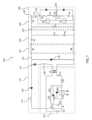
図1は、幾つかの実施形態による、負荷段106を駆動するナノ秒パルサシステム100の回路図である。特定の負荷段106を示しているが、他の様々な負荷が使用されてよい。 FIG. 1 is a circuit diagram of a
幾つかの実施形態では、負荷段106は、半導体処理チャンバ(例えば、プラズマ蒸着システム、半導体組立システム、プラズマスパッタリングシステム等)の理想的又は実効的な回路を表してよい。キャパシタンス12は、例えば、半導体プロセスウェーハがその上に設置されてよい静電チャックのキャパシタンスを表してよい。チャックは、例えば、誘電体材料(例えば、酸化アルミニウム、又は他のセラミック材料、及び誘電体材料内に収容された導体)を含んでよい。例えば、キャパシタ23は、キャパシタンスが小さくてよい(例えば、約10pF、100pF、500pF、1nF、10nF、100nF等であってよい)。 In some embodiments,
キャパシタ13は、例えば、プラズマとウェーハとの間のシースキャパシタンスを表してよい。抵抗56は、例えば、プラズマとウェーハとの間のシース抵抗を表してよい。インダクタ40は、例えば、プラズマとウェーハとの間のシースインダクタンスを表してよい。電流源I2は、例えば、シースを通るイオン電流を表してよい。例えば、キャパシタ23又はキャパシタ13は、キャパシタンスが小さくてよい(例えば、約10pF、100pF、500pF、1nF、10nF、100nF等であってよい)。
キャパシタ18は、例えば、チャンバの壁に対するプラズマシースキャパシタンスを表してよい。抵抗57は、例えば、プラズマとチャンバ壁との間の抵抗を表してよい。電流源I1は、例えば、プラズマ内のイオン電流を表してよい。例えば、キャパシタ23又はキャパシタ18は、キャパシタンスが小さくてよい(例えば、約10pF、100pF、500pF、1nF、10nF、100nF等であってよい)。
幾つかの実施形態では、プラズマ電圧は、接地から測定された回路点123の電圧であってよく、ウェーハ電圧は、接地から測定された回路点122の電圧であり、ウェーハ表面の電圧を表してよく、チャック電圧は、接地から測定された回路点121の電圧であり、電極電圧は、接地から測定された(例えば、電極上の)回路点124の電圧であり、入力電圧は、接地から測定された回路点125の電圧である。 In some embodiments, the plasma voltage may be the voltage at circuit point 123 measured from ground and the wafer voltage is the voltage at
この例では、DCバイアス回路104はバイアス補償を全く含まない。DCバイアス回路104はオフセット電源電圧90を含み、これは、例えば、出力電圧を正バイアス又は負バイアスする。幾つかの実施形態では、オフセット電源電圧90は、ウェーハ電圧とチャック電圧との間の電位を変化させるように調節可能である。幾つかの実施形態では、オフセット電源電圧90は、電圧が約±5kV、±4kV、±3kV、±2kV、±1kV等であってよい。 In this example, DC bias
幾つかの実施形態では、バイアスキャパシタ20は、DCバイアス電圧を他の回路素子から隔離(又は分離)することが可能である。バイアスキャパシタ20は、例えば、回路の1つの部分から別の部分への電位シフトを可能にできる。幾つかの実施形態では、この電位シフトは、ウェーハをチャック上の定位置に保持する静電力が電圧閾値を下回る状態を維持する為に行われてよい。抵抗52は、DCバイアス電源を、ナノ秒パルサ段101からの高電圧パルス出力から隔離することが可能である。 In some embodiments,
バイアスキャパシタ20は、例えば、キャパシタンスが約100pF、10pF、1pF、100μF、10μF、1μF等より小さくてよい。抵抗52は、例えば、抵抗が高くてよく、例えば、抵抗が約1kΩ、10kΩ、100kΩ、1MΩ、10MΩ、100MΩ等であってよい。
抵抗R13は、例えば、高電圧電源システムの出力から電極(例えば、負荷段106)までをつなぐリード又は伝送線の抵抗を表してよい。リード又は伝送線には浮遊キャパシタンスもありうる。 Resistor R13 may represent, for example, the resistance of a lead or transmission line from the output of the high voltage power supply system to the electrode (eg, load stage 106). There may also be stray capacitance in the leads or transmission lines.
幾つかの実施形態では、ナノ秒パルサ段101は、高いパルス電圧(例えば、1kV、10kV、20kV、50kV、100kV等より高い電圧)、高い周波数(例えば、1kHz、10kHz、100kHz、200kHz、500kHz、1MHz等より高い周波数)、速い立ち上がり時間(例えば、約1ns、10ns、50ns、100ns、250ns、500ns、1,000ns等より短い立ち上がり時間)、速い立ち下がり時間(例えば、約1ns、10ns、50ns、100ns、250ns、500ns、1,000ns等より短い立ち下がり時間)、及び/又は短いパルス幅(例えば、約1,000ns、500ns、250ns、100ns、20ns等より短いパルス幅)を有するパルスを発生させてよい。 In some embodiments, the
例えば、ナノ秒パルサ段101は、あらゆる目的の為に本開示に組み込まれている米国特許出願第14/542,487号、件名「高電圧ナノ秒パルサ(High Voltage Nanosecond Pulser)」に記載の任意の装置の全ての部分又は任意の部分、又はあらゆる目的の為に本開示に組み込まれている米国特許出願第14/635,991号、件名「直流的に絶縁された出力可変パルス発生器の開示(Galvanically Isolated Output Variable Pulse Generator Disclosure」に記載の任意の装置の全ての部分又は任意の部分、又はあらゆる目的の為に本開示に組み込まれている米国特許出願第14/798,154号、件名「パルス幅及びパルス繰り返し周波数が可変である高電圧ナノ秒パルサ(High Voltage Nanosecond Pulser With Variable Pulse Width and Pulse Repetition Frequency)」に記載の任意の装置の全ての部分又は任意の部分を含んでよい。 For example,
幾つかの実施形態では、ナノ秒パルサ段101は、任意の様々な様式で互いに結合された1つ以上のナノ秒パルサを含んでよい。 In some embodiments,
幾つかの実施形態では、ナノ秒パルサ段101は、一定のDC電圧を出力するDC電源を含んでよく、DC電源は、スイッチ175によってスイッチングされて、スイッチングされた電力を変圧器85に供給する。DC電源は、オフセット供給電圧90及びエネルギ貯蔵キャパシタ66を含んでよい。変圧器85の巻線比が1:10であれば、変圧器は負荷に対して10kVを発生させることができる。 In some embodiments,
幾つかの実施形態では、負荷キャパシタンス(例えば、キャパシタンス13及びキャパシタンス18)がエネルギ貯蔵キャパシタ66のキャパシタンスに比べて小さければ、変圧器の入力において電圧倍増が行われる場合がある(又は行われない場合がある)。例えば、エネルギ貯蔵キャパシタ66が500Vを供給した場合、変圧器85の入力において1kVが測定される場合がある。 In some embodiments, voltage doubling may (or may not) occur at the input of the transformer if the load capacitances (e.g.,
スイッチ175は、例えば、1つ以上のソリッドステートスイッチを含んでよく、例えば、IGBT、MOSFET、SiC MOSFET、SiC接合トランジスタ、FET、SiCスイッチ、GaNスイッチ、光伝導スイッチ等を含んでよい。スイッチ175は、コントローラからの信号Sig+及びSig-に基づいてスイッチングされてよい。
幾つかの実施形態では、ナノ秒パルサ段101はスナバ回路を含んでよく、スナバ回路は、任意のタイプのスナバ回路を含んでよい。幾つかの実施形態では、スナバ回路はキャパシタを含んでよい。幾つかの実施形態では、スナバ回路はキャパシタ及び抵抗を含んでよい。幾つかの実施形態では、スナバ回路は、キャパシタ、インダクタ、及び抵抗を含んでよい。 In some embodiments,
幾つかの実施形態では、スナバ回路は、スナバ抵抗161、スナバ抵抗161と並列のスナバダイオード163、及びスナバキャパシタ164を含んでよい。スナバ回路は、浮遊インダクタンスを含むこともある。幾つかの実施形態では、スナバ抵抗161及び/又はスナバダイオード163は、スイッチ175のコレクタと変圧器85の一次巻線との間に置かれてよい。スナバダイオード163は、スイッチング時に生じる過電圧を緩衝する為に使用されてよい。スイッチ175のエミッタ側には大容量且つ/又は高速のキャパシタが結合されてよい。スイッチ65のエミッタ側にはフリーホイールダイオード172も結合されてよい。図示していない他の様々な部品も含まれてよい。1つ以上のスイッチ及び/又は回路が並列又は直列に配置されてよい。 In some embodiments, the snubber circuit may include a
幾つかの実施形態では、スイッチ175は、スイッチングされた電圧がフル電圧(例えば、エネルギ貯蔵キャパシタ66及び/又はオフセット供給電圧90の電圧)にならないように高速でスイッチングしてよい。幾つかの実施形態では、スイッチ175と結合されたゲート抵抗が、短いターンオンパルスで設定されてよい。 In some embodiments, switch 175 may switch quickly such that the switched voltage is not at full voltage (eg, the voltage of energy storage capacitor 66 and/or offset supply voltage 90). In some embodiments, a gate resistance coupled to switch 175 may be set with a short turn-on pulse.
幾つかの実施形態では、ナノ秒パルサ段101はフリーホイールダイオード172を含んでよい。幾つかの実施形態では、電流がインダクタを同じ方向に通って流れ続けることを可能にすることによって、誘導負荷に貯蔵されたエネルギが、スイッチ175が開いた後に消散することが可能でありうるように、且つ、エネルギが回路の抵抗素子で消散するように、フリーホイールダイオード172が誘導負荷との組み合わせで使用されてよい。フリーホイールダイオード172が含まれていないと、スイッチ175に大きな逆電圧が発生する可能性がある。 In some embodiments,
幾つかの実施形態では、ナノ秒パルサ段101は、浮遊インダクタンス151及び/又は浮遊抵抗152を含んでよい。浮遊インダクタンス151は、例えば、約10nH、100nH、1,000nH、10,000nH等より小さくてよい。浮遊抵抗152は、例えば、約1Ω、100mΩ、10mΩ等より小さくてよい。 In some embodiments,
幾つかの実施形態では、エネルギ回収回路110は、変圧器の二次側、及び/又はエネルギ貯蔵キャパシタ66と電気的に結合されてよい。エネルギ回収回路110は、例えば、変圧器85の二次側の両端にダイオード130(例えば、クロウバーダイオード)を含んでよい。エネルギ回収回路110は、例えば、(直列に配置された)エネルギ回収ダイオード120及びエネルギ回収インダクタ115を含んでよく、これにより、電流が変圧器85の二次側から流れてエネルギ貯蔵キャパシタ66を充電することを可能にできる。エネルギ回収ダイオード120及びエネルギ回収インダクタ115は、変圧器85の二次側、及びエネルギ貯蔵キャパシタ66に電気的に接続されてよい。幾つかの実施形態では、エネルギ回収回路110は、変圧器85の二次側と電気的に結合されたダイオード130及び/又はインダクタ140を含んでよい。インダクタ140は、浮遊インダクタンスを表してよく、且つ/又は変圧器85の浮遊インダクタンスを含んでよい。 In some embodiments, the
幾つかの実施形態では、エネルギ回収インダクタ115は、任意のタイプのインダクタを含んでよく、例えば、フェライトコアインダクタ又は空芯インダクタを含んでよい。幾つかの実施形態では、エネルギ回収インダクタ115は、任意のタイプのジオメトリを有してよく、例えば、ソレノイド巻線、トロイダル巻線等を有してよい。幾つかの実施形態では、エネルギ回収インダクタ115は、インダクタンスが約10μH、50μH、100μH、500μH等より大きくてよい。幾つかの実施形態では、エネルギ回収インダクタ115は、インダクタンスが約1μH~約100mHであってよい。 In some embodiments,
幾つかの実施形態では、ナノ秒パルサがオンになると、電流が負荷段106を充電する(例えば、キャパシタ13、キャパシタ12、又はキャパシタ18を充電する)ことが可能である。例えば、変圧器85の二次側の電圧がエネルギ貯蔵キャパシタ66の充電電圧より高くなると、幾らかの電流がエネルギ回収インダクタ115を流れることが可能である。ナノ秒パルサがオフになると、電流が負荷段106内のキャパシタ(例えば、キャパシタ52)からエネルギ回収インダクタ115を通って流れて、エネルギ回収インダクタ115の両端の電圧がゼロになるまでエネルギ貯蔵キャパシタ66を充電することが可能である。ダイオード130は、負荷段106内のキャパシタが、負荷段106又はDCバイアス回路104のインダクタンスとリンギングを起こすのを防ぐことが可能である。 In some embodiments, when the nanosecond pulser is turned on, current may charge load stage 106 (eg,
エネルギ回収ダイオード120は、例えば、エネルギ貯蔵キャパシタ66から負荷段106内のキャパシタへ電荷が流れるのを防ぐことが可能である。
エネルギ回収インダクタ115の値は、電流の立ち下がり時間を制御する為に選択されてよい。幾つかの実施形態では、エネルギ回収インダクタ115は、インダクタンスの値が1~600μHであってよい。幾つかの実施形態では、エネルギ回収インダクタ115は、インダクタンスの値が50μHより大きくてよい。幾つかの実施形態では、エネルギ回収インダクタ115は、インダクタンスが約50μH、100μH、150μH、200μH、250μH、300μH、350μH、350μH、400μH、400μH、500μH等より小さくてよい。 The value of
例えば、エネルギ貯蔵キャパシタ66が500Vを供給した場合、(例えば、上述のように電圧倍増によって)変圧器85の入力において1kVが測定されることになる。変圧器85での1kVは、スイッチ175が開いているときに、エネルギ回収回路110の部品間で分割されてよい。それらの値が適切に選択されていれば(例えば、インダクタ162のインダクタンスがエネルギ回収インダクタ115のインダクタンスより小さければ)、エネルギ回収ダイオード120及びエネルギ回収インダクタ115の両端の電圧は500Vより大きくなりうる。そして電流がエネルギ回収ダイオード120を通って流れること及び/又はエネルギ貯蔵キャパシタ66を充電することが可能である。電流は、ダイオードD3及びインダクタ88にも流れうる。エネルギ貯蔵キャパシタ66が充電されたら、電流はもはやダイオードD3及びエネルギ回収インダクタ115には流れなくなりうる。 For example, if energy storage capacitor 66 provided 500V, 1 kV would be measured at the input of transformer 85 (eg, by voltage doubling as described above). The 1 kV at
幾つかの実施形態では、エネルギ回収回路110は、負荷段106からエネルギを転送(又は電荷を転送)することを、例えば、速い時間スケール(例えば、1ns、10ns、50ns、100ns、250n、500ns、1,000ns等の時間スケール)で行ってよい。エネルギ回収回路の浮遊抵抗は、負荷段106の両端のパルスが速い立ち下がり時間tfを有するように小さくてよい。エネルギ回収回路110の浮遊抵抗は、例えば、抵抗が約1Ω、100mΩ、10mΩ等より小さくてよい。幾つかの実施形態では、負荷段106からのエネルギ転送効率が高いことが可能であり、例えば、約60%、70%、80%、又は90%等より高いことが可能である。 In some embodiments,
図1に示した部品のうちの任意の数の部品が必要とされてもされなくてもよく、例えば、ダイオード135又はダイオード130又はインダクタ140は必要とされてもされなくてもよい。 Any number of the components shown in FIG. 1 may or may not be required; for example,
幾つかの実施形態では、電圧源65と、エネルギ回収回路110が電圧源65及び/又はエネルギ貯蔵キャパシタ66に接続している箇所との間にダイオードが置かれてよい。このダイオードは、例えば、電流が電圧源65からエネルギ貯蔵キャパシタ66に流れることを可能にするように配置されてよいが、電流がエネルギ回収回路からエネルギ貯蔵キャパシタ66に流れることを可能にしなくてよい。 In some embodiments, a diode may be placed between
幾つかの実施形態では、エネルギ回収回路110は無くしてもよい。幾つかの実施形態では、抵抗出力段又はバイアス補償回路が含まれてよい。他の様々な回路又は回路素子が含まれてよい。 In some embodiments,
幾つかの実施形態では、別の負荷段106が使用されてよい。幾つかの実施形態では、負荷段は、容量結合プラズマ又は誘導結合プラズマを含んでよい。 In some embodiments, another
幾つかの実施形態では、ナノ秒パルサシステム100は、負荷段106に波形を出力してよい。波形は、複数の高電圧パルスと、それらの高電圧パルスの間の正弦波形とを含んでよい。高電圧パルスは、例えば、約2kVより大きいパルス振幅と、あるパルス幅と、あるパルス繰り返し周波数とを有してよい。正弦波形は、ある波形周波数と、100Vより大きい波形振幅とを有してよい。 In some embodiments,
幾つかの実施形態では、波形周波数及び/又は波形振幅は、ナノ秒パルサシステム100の浮遊インダクタンス及び浮遊キャパシタンスのいずれか又は両方に少なくともある程度依存してよい。浮遊インダクタンスは、例えば、インダクタ87及び/又はインダクタ88のインダクタンスにほぼ依存しうる。別の例として、インダクタ87及び/又はインダクタ88のインダクタンスは、約50nH~約1.8μHであってよい。別の例として、インダクタ87及び/又はインダクタ88のインダクタンスは、約5nH~約20μHであってよい。浮遊キャパシタンスは、例えば、キャパシタ52のキャパシタンスにほぼ依存しうる。キャパシタ52のキャパシタンスは、例えば、約250pF~約1.5nFであってよい。別の例として、キャパシタ52のキャパシタンスは、約50pF~約20nFであってよい。 In some embodiments, the waveform frequency and/or waveform amplitude may depend, at least in part, on either or both of the stray inductance and stray capacitance of the
回路の合計浮遊キャパシタンスは、約50pF~約20nFであってよい。回路の合計浮遊インダクタンスは、約5nH~約20μHであってよい。 The total stray capacitance of the circuit may be about 50 pF to about 20 nF. The total stray inductance of the circuit may be about 5 nH to about 20 μH.
幾つかの実施形態では、波形周波数及び/又は波形振幅は、少なくともある程度はパルス幅にほぼ依存してよい。 In some embodiments, the waveform frequency and/or waveform amplitude may be approximately dependent, at least in part, on the pulse width.
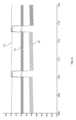
図2は、幾つかの実施形態による、負荷段を駆動する抵抗出力段220を有するナノ秒パルサシステム200の回路図である。この実施例では、エネルギ回収回路110はナノ秒パルサシステム100から無くされており、代わりに抵抗出力段220が置かれている。 FIG. 2 is a circuit diagram of a
抵抗出力段220は、当該技術分野において知られている任意の抵抗出力段を含んでよい。例えば、抵抗出力段220は、あらゆる目的の為に完全な形で本開示に組み込まれている米国特許出願第16/178,538号、件名「高電圧抵抗出力段回路(HIGH VOLTAGE RESISTIVE OUTPUT STAGE CIRCUIT)」に記載の任意の抵抗出力段を含んでよい。
例えば、抵抗出力段220は、インダクタ37、抵抗50、抵抗50、及びキャパシタ19を含んでよい。幾つかの実施形態では、インダクタ37は、インダクタンスが約5~25μHであってよい。幾つかの実施形態では、抵抗50は、抵抗が約50~250Ωであってよい。幾つかの実施形態では、抵抗50は、抵抗出力段220の浮遊抵抗を含んでよい。 For example,
幾つかの実施形態では、抵抗50は、直列及び/又は並列に並んだ複数の抵抗を含んでよい。キャパシタ19は、抵抗50の浮遊キャパシタンスを表してよく、これは、直列及び/又は並列の抵抗の並びのキャパシタンスを含む。浮遊キャパシタンス19のキャパシタンスは、例えば、500pF、250pF、100pF、50pF、10pF、1pF等より小さくてよい。浮遊キャパシタンス19のキャパシタンスは、例えば、負荷キャパシタンスより小さい場合があり、例えば、キャパシタ12、キャパシタ13、及び/又はキャパシタ18等のキャパシタンスより小さい場合がある。 In some embodiments,
幾つかの実施形態では、抵抗50は負荷(例えば、プラズマシースキャパシタンス)を放電してよい。幾つかの実施形態では、抵抗出力段220は、各パルス周期の間の平均電力で約1キロワット超を、且つ/又は各パルス周期におけるエネルギで1ジュール以下を放出するように構成されてよい。幾つかの実施形態では、抵抗出力段220の抵抗50の抵抗は200Ωより小さくてよい。幾つかの実施形態では、抵抗50は、直列又は並列に並んだ複数の抵抗を含んでよく、それらの結合キャパシタンス(例えば、キャパシタ19)は約200pFより小さい。 In some embodiments,
幾つかの実施形態では、抵抗出力段220は、負荷上の電圧波形の形状を制御することに使用可能な回路素子の集合体を含んでよい。幾つかの実施形態では、抵抗出力段220は、受動素子のみ(例えば、抵抗、キャパシタ、インダクタ等)を含んでよい。幾つかの実施形態では、抵抗出力段220は、受動回路素子だけでなく能動回路素子(例えば、スイッチ)を含んでよい。幾つかの実施形態では、抵抗出力段220は、例えば、波形の電圧立ち上がり時間及び/又は波形の電圧立ち下がり時間を制御することに使用されてよい。 In some embodiments,
幾つかの実施形態では、抵抗出力段220は、容量性負荷(例えば、ウェーハ及び/又はプラズマ)を放電させてよい。例えば、これらの容量性負荷はキャパシタンスが小さくてよい(例えば、約10pF、100pF、500pF、1nF、10nF、100nF等であってよい)。 In some embodiments,
幾つかの実施形態では、抵抗出力段220は、パルスのパルス電圧が高く(例えば、1kV、10kV、20kV、50kV、100kV等より高い電圧であり)、且つ/又はパルスの周波数が高く(例えば、1kHz、10kHz、100kHz、200kHz、500kHz、1MHz等より高い周波数であり)、且つ/又はパルスの周波数が約400kHz、0.5MHz、2.0MHz、4.0MHz、13.56MHz、27.12MHz、40.68MHz、50MHz等である回路で使用されてよい。 In some embodiments, the
幾つかの実施形態では、抵抗出力段220は、高い平均電力、高いピーク電力、速い立ち上がり時間、及び/又は速い立ち下がり時間をハンドリングするように選択されてよい。例えば、平均電力定格は、約0.5kW、1.0kW、10kW、25kW等より大きくてよく、且つ/又は、ピーク電力定格は、約1kW、10kW、100kW、1MW等より大きくてよい。 In some embodiments,
幾つかの実施形態では、抵抗出力段220は、受動部品の直列又は並列のネットワークを含んでよい。例えば、抵抗出力段220は、直列の抵抗、キャパシタ、及びインダクタを含んでよい。別の例として、抵抗出力段220は、キャパシタとインダクタの並列の組み合わせに抵抗が直列につながったものを含んでよい。例えば、インダクタ37は、整流器からの出力電圧があるときに抵抗出力段220に有意のエネルギが注入されないようにするのに十分な大きさが選択されてよい。抵抗50及び抵抗50の値は、L/R時間で負荷内のしかるべきキャパシタがRF周波数より速く放電することが可能であるように選択されてよい。 In some embodiments,
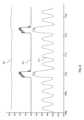
図3は、幾つかの実施形態による、ナノ秒パルサシステム100が発生させる3つの波形を示す。波形310は点124で測定されており、波形315は点122で測定されている(ウェーハ波形)。波形305は、点121で測定された波形と、点122で測定された波形との差である。この例では、ウェーハ波形は、周波数が約19MHzであり、波形ピークツーピーク振幅が約150Vである。この例では、パルス幅は約200nsである。そして、結果として得られるイオン電流は約1アンペアである。 FIG. 3 illustrates three waveforms generated by
波形周波数及び/又は波形振幅は、インダクタ87、インダクタ88、キャパシタ23、キャパシタ12、及びキャパシタ13の値に依存しうる。例えば、インダクタ87及び/又はインダクタ88は、インダクタンスが約500nH、250nH、100nH、50nH、25nH等より小さくてよい。これらの特定の波形の場合、インダクタ87及び/又はインダクタ88は、インダクタンスが約50nHであってよい。キャパシタ23は、キャパシタンスが約1,000pF、500pF、250pF、100pF、50pF等より小さくてよい。これらの特定の波形の場合、キャパシタ23は、キャパシタンスが約250pFであってよい。 The waveform frequency and/or waveform amplitude may depend on the values of
キャパシタ12及びキャパシタ13のキャパシタンスは、負荷106によって固定されてもされなくてもよく、用途に応じて様々であってよい。キャパシタ12は、キャパシタンスが約6.4nFであってよく、キャパシタ13は、キャパシタンスが約25pFであってよい。 The capacitance of
図4は、幾つかの実施形態による、ナノ秒パルサシステム100が発生させる3つの波形を示す。波形410は点124で測定されており、波形415は点122で測定されている(ウェーハ波形)。波形405は、点121で測定された波形と、点122で測定された波形との差である。この例では、ウェーハ波形は、周波数が約19MHzであり、波形ピークツーピーク振幅が約1.75kVである。パルス幅は約350nsである。そして、結果として得られるイオン電流は約1アンペアである。従って、この例では、パルスのパルス幅を250nsから350nsに変更することにより、波形振幅は150Vから1.75kVまで増えた。 FIG. 4 illustrates three waveforms generated by
波形周波数及び/又は波形振幅は、インダクタ87、インダクタ88、キャパシタ23、キャパシタ12、及びキャパシタ13の値に依存しうる。例えば、インダクタ87及び/又はインダクタ88は、インダクタンスが約500nH、250nH、100nH、50nH、25nH等より小さくてよい。これらの特定の波形の場合、インダクタ87及び/又はインダクタ88は、インダクタンスが約50nHであってよい。キャパシタ23は、キャパシタンスが約1,000pF、500pF、250pF、100pF、50pF等より小さくてよい。これらの特定の波形の場合、キャパシタ23は、キャパシタンスが約250pFであってよい。 The waveform frequency and/or waveform amplitude may depend on the values of
キャパシタ12及びキャパシタ13のキャパシタンスは、負荷106によって固定されてもされなくてもよく、用途に応じて様々であってよい。この例では、キャパシタ12は、キャパシタンスが約6.4nFであってよく、キャパシタ13は、キャパシタンスが約25pFであってよい。 The capacitance of
図5は、幾つかの実施形態による、ナノ秒パルサシステム100が発生させる3つの波形を示す。波形510は点124で測定されており、波形515は点122で測定されている(ウェーハ波形)。波形505は、点121で測定された波形と、点122で測定された波形との差である。この例では、ウェーハ波形は、周波数が約19MHzであり、波形ピークツーピーク振幅が約1.75kVである。パルス幅は約1,000nsである。そして、イオン電流は約1アンペアである。 FIG. 5 illustrates three waveforms generated by
波形周波数及び/又は波形振幅は、インダクタ87、インダクタ88、キャパシタ23、キャパシタ12、及びキャパシタ13の値に依存しうる。例えば、インダクタ87及び/又はインダクタ88は、インダクタンスが約500nH、250nH、100nH、50nH、25nH等より小さくてよい。これらの特定の波形の場合、インダクタ87及び/又はインダクタ88は、インダクタンスが約50nHであってよい。キャパシタ23は、キャパシタンスが約1,000pF、500pF、250pF、100pF、50pF等より小さくてよい。これらの特定の波形の場合、キャパシタ23は、キャパシタンスが約250pFであってよい。 The waveform frequency and/or waveform amplitude may depend on the values of
キャパシタ12及びキャパシタ13のキャパシタンスは、負荷106によって固定されてもされなくてもよく、用途に応じて様々であってよい。この例では、キャパシタ12は、キャパシタンスが約6.4nFであってよく、キャパシタ13は、キャパシタンスが約25pFであってよい。 The capacitance of
従って、この例では、パルスのパルス幅を350nsから1,000nsに変更することにより、波形振幅は(約400nsにある)限界に達し、波形ピークツーピーク振幅はほとんど増えない。 Therefore, in this example, by changing the pulse width of the pulse from 350 ns to 1,000 ns, the waveform amplitude reaches a limit (located at approximately 400 ns) and the waveform peak-to-peak amplitude increases little.
図6は、幾つかの実施形態による、ナノ秒パルサシステム100が発生させる3つの波形を示す。波形610は点124で測定されており、波形615は点122で測定されている(ウェーハ波形)。波形605は、点121で測定された波形と、点122で測定された波形との差である。この例では、ウェーハ波形は、周波数が約5.0MHzであり、波形ピークツーピーク振幅が約764Vである。パルス幅は約200nsである。そして、結果として得られるイオン電流は約1アンペアである。 FIG. 6 illustrates three waveforms generated by
波形周波数及び/又は波形振幅は、インダクタ87、インダクタ88、キャパシタ23、キャパシタ12、及びキャパシタ13の値に依存しうる。例えば、インダクタ87及び/又はインダクタ88は、インダクタンスが約500nH、250nH、100nH、50nH、25nH等より小さくてよい。これらの特定の波形の場合、インダクタ87及び/又はインダクタ88は、インダクタンスが約400nHであってよい。例えば、キャパシタ23は、キャパシタンスが約10nF、5nF、1nF、500pF、250pF、100pF、50pF等より小さくてよい。これらの特定の波形の場合、キャパシタ23は、キャパシタンスが約1nFであってよい。 The waveform frequency and/or waveform amplitude may depend on the values of
キャパシタ12及びキャパシタ13のキャパシタンスは、負荷106によって固定されてもされなくてもよく、用途に応じて様々であってよい。この例では、キャパシタ12は、キャパシタンスが約6.4nFであってよく、この例では、キャパシタ13は、キャパシタンスが約1nFであってよい。 The capacitance of
従って、この例では、インダクタ87のインダクタンス、インダクタ88のインダクタンス、及びキャパシタC8のキャパシタンスを増やし、キャパシタ13のキャパシタンスを減らすことにより、波形周波数は約5.0MHzに減った。更に、この例では、パルス幅が約250nsを下回ると(例えば、197nsであると)、それほど大きな波形振幅にはならない。 Therefore, in this example, by increasing the inductance of
図7は、幾つかの実施形態による、ナノ秒パルサシステム100が発生させる3つの波形を示す。波形710は点124で測定されており、波形715は点122で測定されている(ウェーハ波形)。波形705は、点121で測定された波形と、点122で測定された波形との差である。この例では、ウェーハ波形は、周波数が約5.0MHzであり、波形ピークツーピーク振幅が約2.5kVである。パルス幅は約350nsである。そして、結果として得られるイオン電流は約1アンペアである。 FIG. 7 illustrates three waveforms generated by
波形周波数及び/又は波形振幅は、インダクタ87、インダクタ88、キャパシタ23、キャパシタ12、及びキャパシタ13の値に依存しうる。例えば、インダクタ87及び/又はインダクタ88は、インダクタンスが約400nH、250nH、100nH、50nH、25nH等より小さくてよい。これらの特定の波形の場合、インダクタ87及び/又はインダクタ88は、インダクタンスが約400nHであってよい。例えば、キャパシタ23は、キャパシタンスが約10nF、5nF、1nF、500pF、250pF、100pF、50pF等より小さくてよい。これらの特定の波形の場合、キャパシタ23は、キャパシタンスが約1nFであってよい。 The waveform frequency and/or waveform amplitude may depend on the values of
キャパシタ12及びキャパシタ13のキャパシタンスは、負荷106によって固定されてもされなくてもよく、用途に応じて様々であってよい。この例では、キャパシタ12は、キャパシタンスが約6.4nFであってよく、この例では、キャパシタ13は、キャパシタンスが約1nFであってよい。 The capacitance of
従って、この例では、インダクタ87のインダクタンス、及びインダクタ88のインダクタンスを増やすことにより、波形振幅は増えるがパルス振幅は減る。 Therefore, in this example, by increasing the inductance of
図8は、幾つかの実施形態による、ナノ秒パルサシステム100が発生させる3つの波形を示す。波形810は点124で測定されており、波形815は点122で測定されている(ウェーハ波形)。波形805は、点121で測定された波形と、点122で測定された波形との差である。この例では、ウェーハ波形は、周波数が約2.0MHzであり、波形ピークツーピーク振幅が約4.78kVである。パルス幅は約350nsである。そして、結果として得られるイオン電流は約1アンペアである。 FIG. 8 illustrates three waveforms generated by
波形周波数及び/又は波形振幅は、インダクタ87、インダクタ88、キャパシタ23、キャパシタ12、及びキャパシタ13の値に依存しうる。例えば、インダクタ87及び/又はインダクタ88は、インダクタンスが約2,000nH、1,500nH、1,000nH、500nH、100nH、50nH、25nH等であってよい。これらの特定の波形の場合、インダクタ87及び/又はインダクタ88は、インダクタンスが約1,800nHであってよい。例えば、キャパシタ23は、キャパシタンスが約10nF、5nF、1nF、500pF、250pF、100pF、50pF等より小さくてよい。これらの特定の波形の場合、キャパシタ23は、キャパシタンスが約1.5nFであってよい。 The waveform frequency and/or waveform amplitude may depend on the values of
キャパシタ12及びキャパシタ13のキャパシタンスは、負荷106によって固定されてもされなくてもよく、用途に応じて様々であってよい。この例では、キャパシタ12は、キャパシタンスが約6.4nFであってよく、キャパシタ13は、キャパシタンスが約100pFであってよい。 The capacitance of
従って、この例では、インダクタ87のインダクタンス、及びインダクタ88のインダクタンスを増やすことにより、波形振幅は増えるがパルス振幅は減る。 Therefore, in this example, by increasing the inductance of
特に断らない限り、「ほぼ(substantially)」という語は、言及された値の5~10%以内、又は製造公差以内であることを意味する。特に断らない限り、「約(about)」という語は、言及された値の5~10%以内、又は製造公差以内であることを意味する。 Unless otherwise specified, the term "substantially" means within 5-10% of the stated value or within manufacturing tolerances. Unless otherwise specified, the term "about" means within 5-10% of the stated value or within manufacturing tolerances.
「又は(or)」という接続詞は包含的である。 The conjunction "or" is inclusive.
「第1の(first)」、「第2の(second)」、「第3の(third)」等の用語は、各要素を区別する為に使用されており、特に断らない限り、又は順序が明示的に示されるか必要とされるのでない限り、それらの要素の特定の順序を示す為には使用されていない。 Terms such as "first", "second", "third", etc. are used to distinguish between each element, and unless otherwise specified, the order are not used to indicate a specific order of their elements unless explicitly stated or required.
特許請求対象の十分な理解が得られるように、多数の具体的詳細を説明している。しかしながら、当業者であれば理解されるように、それらの具体的詳細がなくても本特許請求対象を実施することは可能である。又、場合によっては、本特許請求対象が曖昧にならないように、当業者にはよく知られているであろう方法、装置、又はシステムについては詳細に説明していない。 Numerous specific details are set forth to provide a thorough understanding of the claimed subject matter. However, one of ordinary skill in the art will understand that the claimed subject matter may be practiced without these specific details. In other instances, methods, apparatus, or systems that are well known to those skilled in the art have not been described in detail to avoid obscuring the claimed subject matter.
記載の1つ以上のシステムは、いかなる特定のハードウェアアーキテクチャ又はハードウェア構成にも限定されない。コンピューティング装置は、1つ以上の入力に対して条件付けられた結果を出力する任意の適切なコンポーネント構成を包含しうる。適切なコンピューティング装置は、汎用コンピューティング装置から、本発明対象の1つ以上の実施形態を実施する専用コンピューティング装置までのコンピューティングシステムをプログラム又は構成する記憶されたソフトウェアにアクセスする、多目的マイクロプロセッサベースのコンピュータシステムを含む。含まれる教示を、コンピューティング装置をプログラム又は構成することに使用されるソフトウェアの形で実施する為に、任意の適切なプログラミング言語、スクリプト言語、又は他のタイプの言語、又は言語の組み合わせが使用されてよい。 The one or more systems described are not limited to any particular hardware architecture or configuration. A computing device may include any suitable component configuration that outputs a result conditioned on one or more inputs. Suitable computing devices include general purpose microcomputing devices that access stored software that programs or configures computing systems ranging from general purpose computing devices to specialized computing devices that implement one or more embodiments of the subject matter of the present invention. Includes processor-based computer systems. Any suitable programming language, scripting language, or other type of language or combination of languages may be used to implement the contained teachings in the form of software used to program or configure a computing device. It's okay to be.
本発明対象を、その特定の実施形態に関して詳細に説明してきたが、当然のことながら、当業者であれば、上述の内容を理解すれば、そのような実施形態の変更物、変形物、及び等価物を容易に生成可能である。従って、当然のことながら、本開示は、限定ではなく例示を目的として示されており、当業者であれば容易に明らかであろうように、本発明対象に対するそのような修正、変形、及び/又は追加を包含することを排除しない。 While the subject matter of the present invention has been described in detail with respect to specific embodiments thereof, it will be appreciated that those skilled in the art will recognize modifications, variations, and modifications to such embodiments upon understanding the foregoing. Equivalents can be easily generated. It should be understood, therefore, that the present disclosure has been presented by way of illustration and not limitation, and is susceptible to such modifications, variations and/or modifications to the subject matter as will be readily apparent to those skilled in the art. or the inclusion of additions.
Claims (30)
Translated fromJapanese前記高電圧電源と電気的に結合されて、前記高電圧電源からの電圧を高い周波数でスイッチングするナノ秒パルサと、
一次側と二次側とを有する変圧器であって、前記ナノ秒パルサは前記変圧器の前記一次側と電気的に結合されている、前記変圧器と、
前記変圧器と電気的に結合されて、波形を発生させる出力であって、前記波形は、
約2kVより大きいパルス振幅と、あるパルス幅と、あるパルス繰り返し周波数とを有する、複数の高電圧パルスと、
ある波形周波数と、100Vより大きい波形振幅とを有する正弦波形であって、前記波形振幅が前記パルス振幅より小さく、前記パルス繰り返し周波数が前記波形周波数より低い、前記正弦波形と、
を含む、前記出力と、
を含む電源。 high voltage power supply,
a nanosecond pulser electrically coupled to the high voltage power source to switch voltage from the high voltage power source at a high frequency;
a transformer having a primary side and a secondary side, the nanosecond pulsar being electrically coupled to the primary side of the transformer;
an output electrically coupled to the transformer to generate a waveform, the waveform comprising:
a plurality of high voltage pulses having a pulse amplitude greater than about 2 kV, a pulse width, and a pulse repetition frequency;
a sinusoidal waveform having a waveform frequency and a waveform amplitude greater than 100V, the waveform amplitude being smaller than the pulse amplitude and the pulse repetition frequency being lower than the waveform frequency;
the output including;
Including power supply.
前記高電圧電源と電気的に結合されたエネルギ回収インダクタと、
前記変圧器の前記二次側と並列に配置されたクロウバーダイオードと、
前記エネルギ回収インダクタと直列に配置されて、電流を負荷から前記エネルギ回収インダクタを経由して前記高電圧電源まで通すように構成された第2のダイオードと、
を含む、
請求項1に記載の電源。 further comprising an energy recovery circuit electrically coupled to the secondary side of the transformer, the energy recovery circuit comprising:
an energy recovery inductor electrically coupled to the high voltage power supply;
a crowbar diode placed in parallel with the secondary side of the transformer;
a second diode placed in series with the energy recovery inductor and configured to pass current from a load through the energy recovery inductor to the high voltage power supply;
including,
The power supply according to claim 1.
前記高電圧電源と電気的に結合されて、前記高電圧電源からの電圧を高い周波数でスイッチングするナノ秒パルサと、
一次側と二次側とを有する変圧器であって、前記ナノ秒パルサは前記変圧器の前記一次側と電気的に結合されている、前記変圧器と、
前記変圧器と電気的に結合されて、波形を発生させる出力であって、前記波形は、
あるパルス振幅と、あるパルス幅と、あるパルス繰り返し周波数とを有する、複数の高電圧パルスと、
ある波形振幅と、ある波形周波数とを有する正弦波形と、
を含む、前記出力と、
前記出力から測定され、キャパシタンスが約20nFより小さい浮遊キャパシタンスと、
前記出力から測定され、インダクタンスが約400nHより小さい浮遊インダクタンスと、
を含む電源。 high voltage power supply,
a nanosecond pulser electrically coupled to the high voltage power source to switch voltage from the high voltage power source at a high frequency;
a transformer having a primary side and a secondary side, the nanosecond pulsar being electrically coupled to the primary side of the transformer;
an output electrically coupled to the transformer to generate a waveform, the waveform comprising:
a plurality of high voltage pulses having a pulse amplitude, a pulse width, and a pulse repetition frequency;
a sine waveform having a certain waveform amplitude and a certain waveform frequency;
the output including;
a stray capacitance measured from the output and having a capacitance of less than about 20 nF;
a stray inductance measured from the output and having an inductance of less than about 400 nH;
Including power supply.
前記高電圧電源と電気的に結合されたエネルギ回収インダクタと、
前記変圧器の前記二次側と並列に配置されたクロウバーダイオードと、
前記エネルギ回収インダクタと直列に配置されて、電流を負荷から前記エネルギ回収インダクタを経由して前記高電圧電源まで通すように構成された第2のダイオードと、
を含む、
請求項11に記載の電源。 further comprising an energy recovery circuit electrically coupled to the secondary side of the transformer, the energy recovery circuit comprising:
an energy recovery inductor electrically coupled to the high voltage power supply;
a crowbar diode placed in parallel with the secondary side of the transformer;
a second diode placed in series with the energy recovery inductor and configured to pass current from a load through the energy recovery inductor to the high voltage power supply;
including,
The power supply according to claim 11.
高電圧電源であって、
高電圧電源と、
前記高電圧電源と電気的に結合されて、前記高電圧電源からの電圧を高い周波数でスイッチングするナノ秒パルサと、
一次側と二次側とを有する変圧器であって、前記ナノ秒パルサは前記変圧器の前記一次側と電気的に結合されている、前記変圧器と、
前記変圧器及び前記プラズマチャンバと電気的に結合されて、前記プラズマチャンバ内で波形を発生させる出力であって、前記波形は、
前記プラズマチャンバ内でプラズマを発生させるように構成された正弦波形であって、ある波形周波数と、100Vより大きい波形振幅とを有する前記正弦波形と、
前記プラズマチャンバ内でプラズマ粒子を加速させる複数の高電圧パルスであって、約2kVより大きいパルス振幅と、あるパルス幅と、あるパルス繰り返し周波数とを有する、前記複数の高電圧パルスと、
を含む、前記出力と、
を含む前記高電圧電源と、
を含む半導体プラズマシステム。 a plasma chamber;
A high voltage power supply,
high voltage power supply,
a nanosecond pulser electrically coupled to the high voltage power source to switch voltage from the high voltage power source at a high frequency;
a transformer having a primary side and a secondary side, the nanosecond pulsar being electrically coupled to the primary side of the transformer;
an output electrically coupled to the transformer and the plasma chamber to generate a waveform in the plasma chamber, the waveform comprising:
a sinusoidal waveform configured to generate a plasma in the plasma chamber, the sinusoidal waveform having a waveform frequency and a waveform amplitude greater than 100V;
a plurality of high voltage pulses that accelerate plasma particles within the plasma chamber, the plurality of high voltage pulses having a pulse amplitude greater than about 2 kV, a pulse width, and a pulse repetition frequency;
the output including;
the high voltage power supply including;
semiconductor plasma systems including;
前記高電圧電源と電気的に結合されたエネルギ回収インダクタと、
前記変圧器の前記二次側と並列に配置されたクロウバーダイオードと、
前記エネルギ回収インダクタと直列に配置されて、電流を負荷から前記エネルギ回収インダクタを経由して前記高電圧電源まで通すように構成された第2のダイオードと、
を含む、
請求項20に記載の半導体プラズマシステム。 The power supply further includes an energy recovery circuit electrically coupled to the secondary side of the transformer, the energy recovery circuit comprising:
an energy recovery inductor electrically coupled to the high voltage power supply;
a crowbar diode placed in parallel with the secondary side of the transformer;
a second diode placed in series with the energy recovery inductor and configured to pass current from a load through the energy recovery inductor to the high voltage power supply;
including,
The semiconductor plasma system according to claim 20.
Applications Claiming Priority (3)
| Application Number | Priority Date | Filing Date | Title |
|---|---|---|---|
| US202063023611P | 2020-05-12 | 2020-05-12 | |
| US63/023,611 | 2020-05-12 | ||
| PCT/US2021/032063WO2021231629A1 (en) | 2020-05-12 | 2021-05-12 | High frequency rf generator and dc pulsing |
Publications (2)
| Publication Number | Publication Date |
|---|---|
| JP2023526229A JP2023526229A (en) | 2023-06-21 |
| JP7439302B2true JP7439302B2 (en) | 2024-02-27 |
Family
ID=78524980
Family Applications (1)
| Application Number | Title | Priority Date | Filing Date |
|---|---|---|---|
| JP2022568727AActiveJP7439302B2 (en) | 2020-05-12 | 2021-05-12 | High frequency RF generator and DC pulsing |
Country Status (5)
| Country | Link |
|---|---|
| US (1) | US20230073797A1 (en) |
| EP (1) | EP4150661A4 (en) |
| JP (1) | JP7439302B2 (en) |
| CN (1) | CN115552571A (en) |
| WO (1) | WO2021231629A1 (en) |
Families Citing this family (1)
| Publication number | Priority date | Publication date | Assignee | Title |
|---|---|---|---|---|
| US11988451B2 (en)* | 2020-04-23 | 2024-05-21 | Brentwood Industries, Inc. | Drift eliminator and method of making |
Citations (3)
| Publication number | Priority date | Publication date | Assignee | Title |
|---|---|---|---|---|
| JP2006158058A (en) | 2004-11-29 | 2006-06-15 | Kasuga Electric Works Ltd | Inverter device |
| WO2020023974A1 (en) | 2018-07-27 | 2020-01-30 | Eagle Harbor Technologies, Inc. | Nanosecond pulser pulse generation |
| US20200043702A1 (en) | 2014-02-28 | 2020-02-06 | Eagle Harbor Technologies, Inc. | High voltage resistive output stage circuit |
Family Cites Families (5)
| Publication number | Priority date | Publication date | Assignee | Title |
|---|---|---|---|---|
| JP4607930B2 (en)* | 2007-09-14 | 2011-01-05 | 株式会社東芝 | Plasma processing apparatus and plasma processing method |
| JP5224837B2 (en)* | 2008-02-01 | 2013-07-03 | 株式会社東芝 | Substrate plasma processing apparatus and plasma processing method |
| US10115567B2 (en)* | 2014-09-17 | 2018-10-30 | Tokyo Electron Limited | Plasma processing apparatus |
| US11302518B2 (en)* | 2018-07-27 | 2022-04-12 | Eagle Harbor Technologies, Inc. | Efficient energy recovery in a nanosecond pulser circuit |
| JP7038901B2 (en)* | 2018-08-10 | 2022-03-18 | イーグル ハーバー テクノロジーズ,インク. | Plasma sheath control for RF plasma reactor |
- 2021
- 2021-05-12JPJP2022568727Apatent/JP7439302B2/enactiveActive
- 2021-05-12CNCN202180034265.1Apatent/CN115552571A/enactivePending
- 2021-05-12EPEP21803769.5Apatent/EP4150661A4/enactivePending
- 2021-05-12WOPCT/US2021/032063patent/WO2021231629A1/ennot_activeCeased
- 2022
- 2022-11-14USUS18/055,411patent/US20230073797A1/enactivePending
Patent Citations (4)
| Publication number | Priority date | Publication date | Assignee | Title |
|---|---|---|---|---|
| JP2006158058A (en) | 2004-11-29 | 2006-06-15 | Kasuga Electric Works Ltd | Inverter device |
| US20200043702A1 (en) | 2014-02-28 | 2020-02-06 | Eagle Harbor Technologies, Inc. | High voltage resistive output stage circuit |
| WO2020023974A1 (en) | 2018-07-27 | 2020-01-30 | Eagle Harbor Technologies, Inc. | Nanosecond pulser pulse generation |
| US20200035457A1 (en) | 2018-07-27 | 2020-01-30 | Eagle Harbor Technologies, Inc. | Nanosecond pulser bias compensation |
Also Published As
| Publication number | Publication date |
|---|---|
| EP4150661A1 (en) | 2023-03-22 |
| US20230073797A1 (en) | 2023-03-09 |
| CN115552571A (en) | 2022-12-30 |
| JP2023526229A (en) | 2023-06-21 |
| WO2021231629A1 (en) | 2021-11-18 |
| EP4150661A4 (en) | 2024-05-29 |
Similar Documents
| Publication | Publication Date | Title |
|---|---|---|
| US11631573B2 (en) | High voltage resistive output stage circuit | |
| US20230336085A1 (en) | Nanosecond pulser bias compensation | |
| JP7285377B2 (en) | Nanosecond Pulser RF Isolation for Plasma Systems | |
| US10460911B2 (en) | High voltage resistive output stage circuit | |
| TWI756551B (en) | High voltage power system and method thereof | |
| JP7622197B2 (en) | Ion Current Droop Compensation | |
| US12437967B2 (en) | Ion current droop compensation | |
| JP7439302B2 (en) | High frequency RF generator and DC pulsing | |
| JP2025020353A (en) | Ion Current Droop Compensation | |
| CN112514254B (en) | Spatially variable wafer bias power system |
Legal Events
| Date | Code | Title | Description |
|---|---|---|---|
| A621 | Written request for application examination | Free format text:JAPANESE INTERMEDIATE CODE: A621 Effective date:20230104 | |
| TRDD | Decision of grant or rejection written | ||
| A977 | Report on retrieval | Free format text:JAPANESE INTERMEDIATE CODE: A971007 Effective date:20240117 | |
| A01 | Written decision to grant a patent or to grant a registration (utility model) | Free format text:JAPANESE INTERMEDIATE CODE: A01 Effective date:20240123 | |
| A61 | First payment of annual fees (during grant procedure) | Free format text:JAPANESE INTERMEDIATE CODE: A61 Effective date:20240214 | |
| R150 | Certificate of patent or registration of utility model | Ref document number:7439302 Country of ref document:JP Free format text:JAPANESE INTERMEDIATE CODE: R150 |