JP7436156B2 - Optical power supply system - Google Patents
Optical power supply systemDownload PDFInfo
- Publication number
- JP7436156B2 JP7436156B2JP2019117970AJP2019117970AJP7436156B2JP 7436156 B2JP7436156 B2JP 7436156B2JP 2019117970 AJP2019117970 AJP 2019117970AJP 2019117970 AJP2019117970 AJP 2019117970AJP 7436156 B2JP7436156 B2JP 7436156B2
- Authority
- JP
- Japan
- Prior art keywords
- power
- power supply
- optical
- laser
- light
- Prior art date
- Legal status (The legal status is an assumption and is not a legal conclusion. Google has not performed a legal analysis and makes no representation as to the accuracy of the status listed.)
- Active
Links
Images


Classifications
- H—ELECTRICITY
- H02—GENERATION; CONVERSION OR DISTRIBUTION OF ELECTRIC POWER
- H02J—CIRCUIT ARRANGEMENTS OR SYSTEMS FOR SUPPLYING OR DISTRIBUTING ELECTRIC POWER; SYSTEMS FOR STORING ELECTRIC ENERGY
- H02J50/00—Circuit arrangements or systems for wireless supply or distribution of electric power
- H02J50/30—Circuit arrangements or systems for wireless supply or distribution of electric power using light, e.g. lasers
- H—ELECTRICITY
- H01—ELECTRIC ELEMENTS
- H01S—DEVICES USING THE PROCESS OF LIGHT AMPLIFICATION BY STIMULATED EMISSION OF RADIATION [LASER] TO AMPLIFY OR GENERATE LIGHT; DEVICES USING STIMULATED EMISSION OF ELECTROMAGNETIC RADIATION IN WAVE RANGES OTHER THAN OPTICAL
- H01S3/00—Lasers, i.e. devices using stimulated emission of electromagnetic radiation in the infrared, visible or ultraviolet wave range
- H01S3/10—Controlling the intensity, frequency, phase, polarisation or direction of the emitted radiation, e.g. switching, gating, modulating or demodulating
- H01S3/10038—Amplitude control
- H01S3/10046—Pulse repetition rate control
- H—ELECTRICITY
- H02—GENERATION; CONVERSION OR DISTRIBUTION OF ELECTRIC POWER
- H02J—CIRCUIT ARRANGEMENTS OR SYSTEMS FOR SUPPLYING OR DISTRIBUTING ELECTRIC POWER; SYSTEMS FOR STORING ELECTRIC ENERGY
- H02J50/00—Circuit arrangements or systems for wireless supply or distribution of electric power
- H02J50/80—Circuit arrangements or systems for wireless supply or distribution of electric power involving the exchange of data, concerning supply or distribution of electric power, between transmitting devices and receiving devices
- H—ELECTRICITY
- H04—ELECTRIC COMMUNICATION TECHNIQUE
- H04B—TRANSMISSION
- H04B10/00—Transmission systems employing electromagnetic waves other than radio-waves, e.g. infrared, visible or ultraviolet light, or employing corpuscular radiation, e.g. quantum communication
- H04B10/80—Optical aspects relating to the use of optical transmission for specific applications, not provided for in groups H04B10/03 - H04B10/70, e.g. optical power feeding or optical transmission through water
- H04B10/806—Arrangements for feeding power
- H04B10/807—Optical power feeding, i.e. transmitting power using an optical signal
Landscapes
- Engineering & Computer Science (AREA)
- Physics & Mathematics (AREA)
- Computer Networks & Wireless Communication (AREA)
- Electromagnetism (AREA)
- Optics & Photonics (AREA)
- Power Engineering (AREA)
- Signal Processing (AREA)
- Plasma & Fusion (AREA)
- Optical Communication System (AREA)
- Semiconductor Lasers (AREA)
Description
Translated fromJapanese本開示は、光給電システムに関する。 The present disclosure relates to an optical power supply system.
近時、電力を光(給電光と呼ばれる)に変換して伝送し、当該給電光を電気エネルギーに変換して電力として利用する光給電システムが研究されている。
特許文献1には、電気信号で変調された信号光、及び電力を供給するための給電光を発信する光発信機と、上記信号光を伝送するコア、上記コアの周囲に形成され上記コアより屈折率が小さく上記給電光を伝送する第1クラッド、及び上記第1クラッドの周囲に形成され上記第1クラッドより屈折率が小さい第2クラッド、を有する光ファイバーと、上記光ファイバーの第1クラッドで伝送された上記給電光を変換した電力で動作し、上記光ファイバーのコアで伝送された上記信号光を上記電気信号に変換する光受信機と、を備えた光通信装置が記載されている。 BACKGROUND ART Recently, research has been carried out on optical power supply systems that convert electric power into light (referred to as power supply light) and transmit it, convert the power supply light into electrical energy, and use the power as electric power.
Patent Document 1 discloses an optical transmitter that transmits signal light modulated by an electric signal and feeding light for supplying electric power, a core that transmits the signal light, and an optical transmitter that is formed around the core and that is connected to the core. an optical fiber having a first cladding having a small refractive index that transmits the feeding light, and a second cladding formed around the first cladding and having a smaller refractive index than the first cladding; and transmitting by the first cladding of the optical fiber. An optical communication device is described, which includes an optical receiver that operates using electric power obtained by converting the supplied power light and converts the signal light transmitted through the core of the optical fiber into the electrical signal.
光給電においては、より一層の光給電効率の向上が求められている。そのための一つとして、給電側及び受電側における光電変換効率の向上が求められている。 In optical power supply, further improvement in optical power supply efficiency is required. As one way to achieve this, there is a need to improve photoelectric conversion efficiency on the power supply side and the power reception side.
本開示の1つの態様の光ファイバー給電システムは、電力によりレーザー発振して給電光をパルス出力する半導体レーザーを含む給電装置と、給電光を電力に変換する光電変換素子を含む受電装置と、受電装置が変換した電力の消費量に応じて、半導体レーザーからの給電量を給電光のパルス幅によって調節する制御装置と、コアとクラッドを有する光ファイバーケーブルと、を備え、前記給電光を前記クラッドで伝送し、前記電力の消費量を伝える信号光とを前記コアで伝送し、
前記受電装置は、前記光電変換素子により変換された電力を外部機器用に出力可能とし、
前記給電装置と前記受電装置とは、互いにデータ通信を行うデータ通信装置の一方と他方とに設けられ、
他方の前記データ通信装置の通信機能によって前記外部機器の電力消費量を前記受電装置側に送信する。 An optical fiber power supply system according to one aspect of the present disclosure includes a power supply device including a semiconductor laser that outputs a pulse of power supply light by laser oscillation using electric power, a power reception device including a photoelectric conversion element that converts the power supply light into electric power, and a power reception device. a control device that adjusts the amount of power supplied from the semiconductor laser by the pulse width of the power supply light according to the consumption amount of the power converted by the semiconductor laser; and an optical fiber cable having a core and a cladding, the power supply light is transmitted by the cladding. andtransmitting a signal light that conveys the amount of power consumption through the core,
The power receiving device is capable of outputting the power converted by the photoelectric conversion element for external equipment,
The power feeding device and the power receiving device are provided in one and the other of data communication devices that perform data communication with each other,
A communication function of the other data communication device transmits the power consumption of the external device to the power receiving device .
本開示の1つの態様の光給電システムによれば、給電側及び受電側における光給電効率の向上を図ることが可能となる。 According to the optical power supply system of one aspect of the present disclosure, it is possible to improve the optical power supply efficiency on the power supply side and the power reception side.
以下に本開示の一実施形態につき図面を参照して説明する。 An embodiment of the present disclosure will be described below with reference to the drawings.
(1)システム概要
〔第1実施形態〕
図1に示すように本実施形態の光給電システムとしての光ファイバー給電(PoF:Power over Fiber)システム1Aは、給電装置(PSE:Power Sourcing Equipment)110と、光ファイバーケーブル200Aと、受電装置(PD:Powered Device)310を備える。
なお、本開示における給電装置は電力を光エネルギーに変換して供給する装置であり、受電装置は光エネルギーの供給を受け当該光エネルギーを電力に変換する装置である。
給電装置110は、給電用半導体レーザー111を含む。
光ファイバーケーブル200Aは、給電光の伝送路を形成する光ファイバー250Aを含む。
受電装置310は、光電変換素子311を含む。(1) System overview [First embodiment]
As shown in FIG. 1, an optical fiber power supply (PoF: Power over Fiber)
Note that the power feeding device in the present disclosure is a device that converts electric power into optical energy and supplies the same, and the power receiving device is a device that receives optical energy and converts the optical energy into electric power.
The
The
給電装置110は電源に接続され、給電用半導体レーザー111等が電気駆動される。
給電用半導体レーザー111は、上記電源からの電力によりレーザー発振して給電光112を出力する。 The
The power
光ファイバーケーブル200Aは、一端201Aが給電装置110に接続可能とされ、他端202Aが受電装置310に接続可能とされ、給電光112を伝送する。
給電装置110からの給電光112が、光ファイバーケーブル200Aの一端201Aに入力され、給電光112は光ファイバー250A中を伝搬し、他端202Aから受電装置310に出力される。 The
光電変換素子311は、光ファイバーケーブル200Aを通して伝送されてきた給電光112を電力に変換する。光電変換素子311により変換された電力が、受電装置310内で必要な駆動電力とされる。さらに受電装置310は光電変換素子311により変換された電力を外部機器用に出力可能とされる。 The
給電用半導体レーザー111及び光電変換素子311の光‐電気間の変換効果を奏する半導体領域を構成する半導体材料が500nm以下の短波長のレーザー波長をもった半導体とされる。
短波長のレーザー波長をもった半導体は、バンドギャップが大きく光電変換効率が高いので、光給電の発電側及び受電側における光電変換効率が向上され、光給電効率が向上する。
そのためには、同半導体材料として、例えば、ダイヤモンド、酸化ガリウム、窒化アルミニウム、GaN等、レーザー波長(基本波)が200~500nmのレーザー媒体の半導体材料を用いてもよい。
また、同半導体材料として、2.4eV以上のバンドギャップを有した半導体が適用される。
例えば、ダイヤモンド、酸化ガリウム、窒化アルミニウム、GaN等、バンドギャップ2.4~6.2eVのレーザー媒体の半導体材料を用いてもよい。
なお、レーザー光は長波長ほど伝送効率が良く、短波長ほど光電変換効率が良い傾向にある。したがって、長距離伝送の場合には、レーザー波長(基本波)が500nmより大きいレーザー媒体の半導体材料を用いてもよい。また、光電変換効率を優先する場合には、レーザー波長(基本波)が200nmより小さいレーザー媒体の半導体材料を用いてもよい。
これらの半導体材料は、給電用半導体レーザー111及び光電変換素子311のいずれか一方に適用してもよい。給電側又は受電側における光電変換効率が向上され、光給電効率が向上する。 The semiconductor material constituting the semiconductor region of the power
A semiconductor with a short laser wavelength has a large band gap and high photoelectric conversion efficiency, so the photoelectric conversion efficiency on the power generation side and the power receiving side of optical power supply is improved, and the optical power supply efficiency is improved.
For this purpose, a semiconductor material of a laser medium having a laser wavelength (fundamental wave) of 200 to 500 nm, such as diamond, gallium oxide, aluminum nitride, or GaN, may be used as the semiconductor material.
Further, as the semiconductor material, a semiconductor having a band gap of 2.4 eV or more is applied.
For example, a semiconductor material of the laser medium with a band gap of 2.4 to 6.2 eV, such as diamond, gallium oxide, aluminum nitride, or GaN, may be used.
Note that the longer the wavelength of laser light, the better the transmission efficiency, and the shorter the wavelength, the better the photoelectric conversion efficiency. Therefore, in the case of long-distance transmission, a semiconductor material of the laser medium with a laser wavelength (fundamental wave) greater than 500 nm may be used. Further, when giving priority to photoelectric conversion efficiency, a semiconductor material of a laser medium having a laser wavelength (fundamental wave) smaller than 200 nm may be used.
These semiconductor materials may be applied to either the power
〔第2実施形態〕
図2に示すように本実施形態の光給電システムとしての光ファイバー給電(PoF:Power over Fiber)システム1は、光ファイバーを介した光給電システムと光通信システムとを含むものであり、給電装置(PSE:Power Sourcing Equipment)110を含む第1のデータ通信装置100と、光ファイバーケーブル200と、受電装置(PD:Powered Device)310を含む第2のデータ通信装置300とを備える。
なお、以下の説明では、原則として、既に説明された構成については同一の符号を付して、特に言及がない場合には既に説明された構成と同一の構成とする。
給電装置110は、給電用半導体レーザー111を含む。第1のデータ通信装置100は、給電装置110のほか、データ通信を行う発信部120と、受信部130とを含む。第1のデータ通信装置100は、データ端末装置(DTEP(Date Terminal Equipment))、中継器(Repeater)等に相当する。発信部120は、信号用半導体レーザー121と、モジュレーター122とを含む。受信部130は、信号用フォトダイオード131を含む。[Second embodiment]
As shown in FIG. 2, a power over fiber (PoF) system 1 as an optical power supply system of this embodiment includes an optical power supply system and an optical communication system via optical fibers, and includes a power supply device (PSE). The
In the following description, in principle, the same reference numerals are given to the configurations that have already been described, and unless otherwise mentioned, the same configurations are assumed to be the same as the configurations that have already been described.
The
光ファイバーケーブル200は、信号光の伝送路を形成するコア210と、コア210の外周に配置され、給電光の伝送路を形成するクラッド220と有する光ファイバー250を含む。 The
受電装置310は、光電変換素子311を含む。第2のデータ通信装置300は、受電装置310のほか、発信部320と、受信部330と、データ処理ユニット340とを含む。第2のデータ通信装置300は、パワーエンドステーション(Power End Station)
等に相当する。発信部320は、信号用半導体レーザー321と、モジュレーター322とを含む。受信部330は、信号用フォトダイオード331を含む。データ処理ユニット340は、受信した信号を処理するユニットである。また、第2のデータ通信装置300は、通信ネットワークにおけるノードである。または第2のデータ通信装置300は、他のノードと通信するノードでもよい。
etc. The
第1のデータ通信装置100は電源に接続され、給電用半導体レーザー111、信号用半導体レーザー121と、モジュレーター122、信号用フォトダイオード131等が電気駆動される。また、第1のデータ通信装置100は、通信ネットワークにおけるノードである。または第1のデータ通信装置100は、他のノードと通信するノードでもよい。
給電用半導体レーザー111は、上記電源からの電力によりレーザー発振して給電光112を出力する。 The first
The power
光電変換素子311は、光ファイバーケーブル200を通して伝送されてきた給電光112を電力に変換する。光電変換素子311により変換された電力は、発信部320、受信部330及びデータ処理ユニット340の駆動電力、その他の第2のデータ通信装置300内で必要となる駆動電力とされる。さらに第2のデータ通信装置300は、光電変換素子311により変換された電力を外部機器用に出力可能とされていてもよい。 The
一方、発信部120のモジュレーター122は、信号用半導体レーザー121からのレーザー光123を送信データ124に基づき変調して信号光125として出力する。
受信部330の信号用フォトダイオード331は、光ファイバーケーブル200を通して伝送されてきた信号光125を電気信号に復調し、データ処理ユニット340に出力する。データ処理ユニット340は、当該電気信号によるデータをノードに送信し、その一方で当該ノードからデータを受信し、送信データ324としてモジュレーター322に出力する。
発信部320のモジュレーター322は、信号用半導体レーザー321からのレーザー光323を送信データ324に基づき変調して信号光325として出力する。
受信部130の信号用フォトダイオード131は、光ファイバーケーブル200を通して伝送されてきた信号光325を電気信号に復調し出力する。当該電気信号によるデータがノードに送信され、その一方で当該ノードからのデータが送信データ124とされる。 On the other hand, the
The
The
The
第1のデータ通信装置100からの給電光112及び信号光125が、光ファイバーケーブル200の一端201に入力され、給電光112はクラッド220を伝搬し、信号光125はコア210を伝搬し、他端202から第2のデータ通信装置300に出力される。
第2のデータ通信装置300からの信号光325が、光ファイバーケーブル200の他端202に入力され、コア210を伝搬し、一端201から第1のデータ通信装置100に出力される。 A
Signal light 325 from the second
なお、図3に示すように第1のデータ通信装置100に光入出力部140とこれに付設された光コネクタ141が設けられる。また、第2のデータ通信装置300に光入出力部350とこれに付設された光コネクタ351が設けられる。光ファイバーケーブル200の一端201に設けられた光コネクタ230が光コネクタ141に接続する。光ファイバーケーブル200の他端202に設けられた光コネクタ240が光コネクタ351に接続する。光入出力部140は、給電光112をクラッド220に導光し、信号光125をコア210に導光し、信号光325を受信部130に導光する。光入出力部350は、給電光112を受電装置310に導光し、信号光125を受信部330に導光し、信号光325をコア210に導光する。
以上のように、光ファイバーケーブル200は、一端201が第1のデータ通信装置100に接続可能とされ、他端202が第2のデータ通信装置300に接続可能とされ、給電光112を伝送する。さらに本実施形態では、光ファイバーケーブル200は、信号光125,325を双方向伝送する。 Note that, as shown in FIG. 3, the first
As described above, the
給電用半導体レーザー111及び光電変換素子311の光‐電気間の変換効果を奏する半導体領域を構成する半導体材料としては上記第1実施形態と同様のものが適用され、高い光給電効率が実現される。 The same semiconductor materials as in the first embodiment are used as the semiconductor materials constituting the semiconductor regions of the power feeding
なお、図4に示す光給電システムとしての光ファイバー給電システム1Bの光ファイバーケーブル200Bのように、信号光を伝送する光ファイバー260と、給電光を伝送する光ファイバー270とを別々に設けてもよい。光ファイバーケーブル200Bも複数本で構成してもよい。 Note that, like an
(2)給電用半導体レーザーがパルス出力を行う構成について
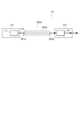
次に、給電用半導体レーザーがパルス出力を行う構成について図5を参照して説明する。
図5は給電用半導体レーザー111がパルス出力を行う光ファイバー給電システム1の構成図である。
第1のデータ通信装置100の給電用半導体レーザー111がパルス出力を行うために、例えば、給電用半導体レーザー111の励起源のON(点灯状態)とOFF(消灯状態)とを切り替える制御装置150が設けられている。
この制御装置150は、一定周期で連続的にONとOFFと交互に繰り返すと共に、ON期間の比率(デューティー比)を増減させて出力を調節するPWM(Pulse Width Modulation)制御を実施する。
制御装置150は、マイクロコンピュータから構成されてもよいし、アナログ回路又はデジタル回路を利用したシーケンサから構成されてもよい。(2) Regarding the configuration in which the power feeding semiconductor laser outputs pulses Next, the configuration in which the power feeding semiconductor laser outputs pulses will be described with reference to FIG. 5.
FIG. 5 is a configuration diagram of the optical fiber power feeding system 1 in which the power feeding
In order for the power
This
The
一方、第2のデータ通信装置300の光電変換素子311は、図6の点線Pに示すように、パルス出力された給電光112を受光してパルス的に電力を出力する。
そして、図5に示すように、光電変換素子311には、パルス的に出力される電力を平滑化する電力平滑化デバイス360が併設されている。この電力平滑化デバイス360は、平滑化回路を含み、周期的にONとOFFを繰り返す電力を平滑化し、図6の実線Fに示すように、周期的に緩やかな増加と減少を繰り返す平滑化電力に変換して、電力供給先となる第2のデータ通信装置300の各構成や外部機器等の負荷370に入力する。なお、電力平滑化デバイス360は、増減しないほぼ一定の電力を出力可能な平滑化回路を有する構成としてもよい。 On the other hand, the
As shown in FIG. 5, the
また、第2のデータ通信装置300は、受電装置310から電力平滑化デバイス360を介して出力された電力を消費する消費先である負荷370における電力消費量を検出する検出部380を備えている。
検出部380は、負荷370に流れる電流を検出する電流検出抵抗によって検出する構成、負荷370に流れる電流の経路の周囲に配置した磁気コアの磁束密度から検出する構成、その他、電力検出を行う各種の周知の構成を利用することができる。 The second
The
検出部380により検出された負荷370における電力消費量は、データ処理ユニット340に入力される。
データ処理ユニット340は、検出部380により検出された負荷370における電力消費量を送信データ324に含ませて発信部320のモジュレーター322に出力する。これにより、発信部320のモジュレーター322は、信号用半導体レーザー321からのレーザー光323を送信データ324に基づき変調して信号光325として出力する。 The power consumption amount in the
The
前述した第1のデータ通信装置100の制御装置150は、発信部320から伝送されてきた信号光325から復調された送信データ324を受信部130から取得し、送信データ324に含まれる負荷370における電力消費量を読み取ることができる。そして、制御装置150は、負荷370における電力消費量に応じて、給電用半導体レーザー111のデューティー比を増減させて出力を調節する制御を行う。
例えば、第2のデータ通信装置300側の電力消費量が低減又は規定値よりも少量となる場合には、給電用半導体レーザー111のレーザー出力を低減させて、第2のデータ通信装置300側への電力供給量を低減する。また、第2のデータ通信装置300側の電力消費量が増加又は規定値よりも多量となる場合には、給電用半導体レーザー111のレーザー出力を増加させて、第2のデータ通信装置300側への電力供給量を増加させる。 The
For example, when the power consumption on the second
このように、図5に示す光ファイバー給電システム1では、半導体レーザー111が給電光をパルス出力するので、レーザー波長を一定に維持したまま電力供給量の制御を容易に行うことが可能となる。例えば、半導体レーザー111の給電光のパルス出力のデューティー比を変更することで比例的に電力供給量を増減させることができ、電力供給量をより適正に制御することが可能となる。
また、制御装置150は、受電装置310又は負荷370側で検出された電力消費量に応じて、半導体レーザー111からの給電光112による給電量を調節するので、消費電力に応じて適正な給電量で給電を行うことができ、受電装置310で余剰となる電力消費量を低減することができ、光給電効率の向上を図ることが可能となる。
また、受電装置310側には、受電装置310が変換した電力を平滑化する電力平滑化デバイス360が設けられているので、変動の少ない安定的な電力供給を行うことが可能となる。 In this way, in the optical fiber power supply system 1 shown in FIG. 5, the
Furthermore, the
Further, since a
図5では給電用半導体レーザーがパルス出力を行う構成を光ファイバー給電システム1に適用した例を示しているが、図5と同じように、給電用半導体レーザーがパルス出力を行う構成を光ファイバー給電システム1Bにも適用することが可能である。 Although FIG. 5 shows an example in which a configuration in which a semiconductor laser for power supply outputs pulses is applied to the optical fiber power supply system 1, similarly to FIG. 5, a configuration in which a semiconductor laser for power supply outputs pulses is applied to an optical fiber
以上本開示の実施形態を説明したが、この実施形態は、例として示したものであり、この他の様々な形態で実施が可能であり、発明の要旨を逸脱しない範囲で、構成要素の省略、置き換え、変更を行うことができる。 Although the embodiment of the present disclosure has been described above, this embodiment is shown as an example, and it can be implemented in various other forms, and components may be omitted without departing from the gist of the invention. , can be replaced or modified.
1,1A,1B 光ファイバー給電システム(光給電システム)
100 第1のデータ通信装置
110 給電装置
111 給電用半導体レーザー
112 給電光
120 発信部
121 信号用半導体レーザー
122 モジュレーター
123 レーザー光
124 送信データ
125 信号光
130 受信部
131 信号用フォトダイオード
140 光入出力部
141 光コネクタ
150 制御装置
200 光ファイバーケーブル
200A 光ファイバーケーブル
200B 光ファイバーケーブル
230 光コネクタ
240 光コネクタ
250,250A,260,270 光ファイバー
300 第2のデータ通信装置
310 受電装置
311 光電変換素子
320 発信部
321 信号用半導体レーザー
322 モジュレーター
323 レーザー光
324 送信データ
325 信号光
330 受信部
331 信号用フォトダイオード
340 データ処理ユニット
350 光入出力部
351 光コネクタ
360 電力平滑化デバイス
370 負荷
380 検出部1, 1A, 1B Optical fiber power supply system (optical power supply system)
100 First
Claims (5)
Translated fromJapanese前記給電光を電力に変換する光電変換素子を含む受電装置と、
前記受電装置が変換した電力の消費量に応じて、前記半導体レーザーからの給電量を前記給電光のパルス幅によって調節する制御装置と、
コアとクラッドを有する光ファイバーケーブルと、
を備え、
前記給電光を前記クラッドで伝送し、前記電力の消費量を伝える信号光を前記コアで伝送し、
前記受電装置は、前記光電変換素子により変換された電力を外部機器用に出力可能とし、
前記給電装置と前記受電装置とは、互いにデータ通信を行うデータ通信装置の一方と他方とに設けられ、
他方の前記データ通信装置の通信機能によって前記外部機器の電力消費量を前記受電装置側に送信する
光給電システム。 a power supply device including a semiconductor laser that outputs a pulse of power supply light by laser oscillation using electric power;
a power receiving device including a photoelectric conversion element that converts the power supply light into electric power;
a control device that adjusts the amount of power supplied from the semiconductor laser by the pulse width of the power supply light according to the consumption amount of power converted by the power receiving device;
an optical fiber cable having a core and a cladding;
Equipped with
transmitting the power supply light through the cladding,transmitting a signal light that conveys the power consumption through the core;
The power receiving device is capable of outputting the power converted by the photoelectric conversion element for external equipment,
The power feeding device and the power receiving device are provided in one and the other of data communication devices that perform data communication with each other,
transmitting the power consumption of the external device to the power receiving device side using the communication function of the other data communication device;
Optical power supply system.
Priority Applications (3)
| Application Number | Priority Date | Filing Date | Title |
|---|---|---|---|
| JP2019117970AJP7436156B2 (en) | 2019-06-26 | 2019-06-26 | Optical power supply system |
| US17/612,219US12027883B2 (en) | 2019-06-26 | 2020-06-10 | Optical power supply system with adjustment of feed light supply based on electric power consumption |
| PCT/JP2020/022786WO2020261987A1 (en) | 2019-06-26 | 2020-06-10 | Optical power supply system |
Applications Claiming Priority (1)
| Application Number | Priority Date | Filing Date | Title |
|---|---|---|---|
| JP2019117970AJP7436156B2 (en) | 2019-06-26 | 2019-06-26 | Optical power supply system |
Publications (2)
| Publication Number | Publication Date |
|---|---|
| JP2021005767A JP2021005767A (en) | 2021-01-14 |
| JP7436156B2true JP7436156B2 (en) | 2024-02-21 |
Family
ID=74059752
Family Applications (1)
| Application Number | Title | Priority Date | Filing Date |
|---|---|---|---|
| JP2019117970AActiveJP7436156B2 (en) | 2019-06-26 | 2019-06-26 | Optical power supply system |
Country Status (3)
| Country | Link |
|---|---|
| US (1) | US12027883B2 (en) |
| JP (1) | JP7436156B2 (en) |
| WO (1) | WO2020261987A1 (en) |
Families Citing this family (2)
| Publication number | Priority date | Publication date | Assignee | Title |
|---|---|---|---|---|
| US11575055B2 (en) | 2019-07-15 | 2023-02-07 | SLT Technologies, Inc | Methods for coupling of optical fibers to a power photodiode |
| GB2628107B (en)* | 2023-03-13 | 2025-03-12 | Space Power Ltd | Determination of preferred wireless power transmission mode |
Family Cites Families (7)
| Publication number | Priority date | Publication date | Assignee | Title |
|---|---|---|---|---|
| JPH02168397A (en)* | 1988-12-22 | 1990-06-28 | Toshiba Corp | Optical energy-driven detection device |
| JPH10510418A (en)* | 1994-12-14 | 1998-10-06 | シーメンス アクチエンゲゼルシヤフト | Method and apparatus for providing a regulated supply voltage or regulated supply current to an electrical load |
| JPH1189120A (en)* | 1997-09-08 | 1999-03-30 | Nippon Telegr & Teleph Corp <Ntt> | Optical power transmission method and apparatus |
| JP2010135989A (en) | 2008-12-03 | 2010-06-17 | Mitsubishi Electric Corp | Optic fiber, optical communication device, and optical communication method |
| US9197329B2 (en)* | 2010-05-11 | 2015-11-24 | The Invention Science Fund I, Llc | Optical power transmission packeting systems and methods |
| EP3420376A1 (en)* | 2016-02-22 | 2019-01-02 | Lasermotive, Inc. | Remote power safety system |
| US10879741B2 (en)* | 2019-05-31 | 2020-12-29 | At&T Intellectual Property I, L.P. | Wireless power transfer network management |
- 2019
- 2019-06-26JPJP2019117970Apatent/JP7436156B2/enactiveActive
- 2020
- 2020-06-10USUS17/612,219patent/US12027883B2/enactiveActive
- 2020-06-10WOPCT/JP2020/022786patent/WO2020261987A1/ennot_activeCeased
Non-Patent Citations (1)
| Title |
|---|
| Motoharu Matsuura and Jun Sato,Bidirectional Radio-Over-Fiber Systems Using Double-Clad Fibers for Optically Powered Remote Antenna Units,IEEE Photonics Journal [online],2014年,Vol. 7, No. 1,[retrieved on 2023.04.28], Retrieved from the Internet : <URL: https://ieeexplore.ieee.org/stamp/stamp.jsp?tp=&arnumber=6987243>,<DOI: 10.1109/JPHOT.2014.2381669> |
Also Published As
| Publication number | Publication date |
|---|---|
| WO2020261987A1 (en) | 2020-12-30 |
| US20220311282A1 (en) | 2022-09-29 |
| US12027883B2 (en) | 2024-07-02 |
| JP2021005767A (en) | 2021-01-14 |
Similar Documents
| Publication | Publication Date | Title |
|---|---|---|
| JP7344750B2 (en) | Optical power supply system | |
| EP3742631B1 (en) | Pse device and powered device of optical power supply system, and optical power supply system | |
| WO2021014734A1 (en) | Fiber optic power supply system | |
| CN113243071B (en) | Power receiving device and optical fiber power supply system | |
| JP7436156B2 (en) | Optical power supply system | |
| WO2021079703A1 (en) | Optical power supply system | |
| WO2021014841A1 (en) | Light power supply system | |
| CN113544938B (en) | Power receiving device of optical power supply system, power supply device and optical power supply system | |
| US12250087B2 (en) | Power-over-fiber system | |
| CN113544936B (en) | Optical power supply system | |
| JP6790190B1 (en) | Fiber optic power supply system | |
| JP7344698B2 (en) | Fiber optic power supply system | |
| JP7398240B2 (en) | Power receiving device, power feeding device, and optical fiber power feeding system | |
| WO2021075087A1 (en) | Optical fiber power feeding system | |
| JP7436160B2 (en) | Optical power supply system | |
| JP6890635B2 (en) | Optical power supply system | |
| JP6898391B2 (en) | Fiber optic power supply system | |
| JP6889226B2 (en) | Optical power supply system power receiving device and power supply device and optical power supply system | |
| JP6889227B2 (en) | Optical power supply system power receiving device and power supply device and optical power supply system | |
| JP7326107B2 (en) | Power receiving device and optical fiber power supply system | |
| JP7308682B2 (en) | Optical power supply system |
Legal Events
| Date | Code | Title | Description |
|---|---|---|---|
| A621 | Written request for application examination | Free format text:JAPANESE INTERMEDIATE CODE: A621 Effective date:20211210 | |
| A131 | Notification of reasons for refusal | Free format text:JAPANESE INTERMEDIATE CODE: A131 Effective date:20230124 | |
| A521 | Request for written amendment filed | Free format text:JAPANESE INTERMEDIATE CODE: A523 Effective date:20230308 | |
| A131 | Notification of reasons for refusal | Free format text:JAPANESE INTERMEDIATE CODE: A131 Effective date:20230516 | |
| A521 | Request for written amendment filed | Free format text:JAPANESE INTERMEDIATE CODE: A523 Effective date:20230712 | |
| A02 | Decision of refusal | Free format text:JAPANESE INTERMEDIATE CODE: A02 Effective date:20231017 | |
| A521 | Request for written amendment filed | Free format text:JAPANESE INTERMEDIATE CODE: A523 Effective date:20231227 | |
| A911 | Transfer to examiner for re-examination before appeal (zenchi) | Free format text:JAPANESE INTERMEDIATE CODE: A911 Effective date:20240110 | |
| TRDD | Decision of grant or rejection written | ||
| A01 | Written decision to grant a patent or to grant a registration (utility model) | Free format text:JAPANESE INTERMEDIATE CODE: A01 Effective date:20240206 | |
| A61 | First payment of annual fees (during grant procedure) | Free format text:JAPANESE INTERMEDIATE CODE: A61 Effective date:20240208 | |
| R150 | Certificate of patent or registration of utility model | Ref document number:7436156 Country of ref document:JP Free format text:JAPANESE INTERMEDIATE CODE: R150 |