JP7415820B2 - antenna device - Google Patents
antenna deviceDownload PDFInfo
- Publication number
- JP7415820B2 JP7415820B2JP2020110670AJP2020110670AJP7415820B2JP 7415820 B2JP7415820 B2JP 7415820B2JP 2020110670 AJP2020110670 AJP 2020110670AJP 2020110670 AJP2020110670 AJP 2020110670AJP 7415820 B2JP7415820 B2JP 7415820B2
- Authority
- JP
- Japan
- Prior art keywords
- plate
- antenna
- antenna device
- ground
- ground plate
- Prior art date
- Legal status (The legal status is an assumption and is not a legal conclusion. Google has not performed a legal analysis and makes no representation as to the accuracy of the status listed.)
- Active
Links
- 239000004020conductorSubstances0.000claimsdescription151
- 230000005404monopoleEffects0.000claimsdescription5
- 238000010586diagramMethods0.000description13
- 238000004891communicationMethods0.000description12
- 239000003566sealing materialSubstances0.000description10
- 229920005989resinPolymers0.000description9
- 239000011347resinSubstances0.000description9
- 238000004088simulationMethods0.000description7
- 230000000694effectsEffects0.000description6
- 230000005684electric fieldEffects0.000description6
- 238000000034methodMethods0.000description6
- 238000012986modificationMethods0.000description6
- 230000004048modificationEffects0.000description6
- RYGMFSIKBFXOCR-UHFFFAOYSA-NCopperChemical compound[Cu]RYGMFSIKBFXOCR-UHFFFAOYSA-N0.000description5
- 238000010168coupling processMethods0.000description5
- 238000000605extractionMethods0.000description5
- 239000003989dielectric materialSubstances0.000description4
- 239000000463materialSubstances0.000description4
- 238000004904shorteningMethods0.000description4
- 230000005540biological transmissionEffects0.000description3
- 229910052802copperInorganic materials0.000description3
- 239000010949copperSubstances0.000description3
- 230000008878couplingEffects0.000description3
- 238000005859coupling reactionMethods0.000description3
- 238000009826distributionMethods0.000description3
- 239000003822epoxy resinSubstances0.000description3
- 238000009434installationMethods0.000description3
- 229920000647polyepoxidePolymers0.000description3
- 230000005855radiationEffects0.000description3
- 125000000391vinyl groupChemical group[H]C([*])=C([H])[H]0.000description3
- 229920002554vinyl polymerPolymers0.000description3
- 239000004743PolypropyleneSubstances0.000description2
- XECAHXYUAAWDEL-UHFFFAOYSA-Nacrylonitrile butadiene styreneChemical compoundC=CC=C.C=CC#N.C=CC1=CC=CC=C1XECAHXYUAAWDEL-UHFFFAOYSA-N0.000description2
- 229920000122acrylonitrile butadiene styrenePolymers0.000description2
- 239000004676acrylonitrile butadiene styreneSubstances0.000description2
- 238000006243chemical reactionMethods0.000description2
- 239000011889copper foilSubstances0.000description2
- 239000011521glassSubstances0.000description2
- 239000002184metalSubstances0.000description2
- 229910052751metalInorganic materials0.000description2
- 239000004417polycarbonateSubstances0.000description2
- 229920000515polycarbonatePolymers0.000description2
- 229920001155polypropylenePolymers0.000description2
- 230000002441reversible effectEffects0.000description2
- 239000000758substrateSubstances0.000description2
- 239000010409thin filmSubstances0.000description2
- RNFJDJUURJAICM-UHFFFAOYSA-N2,2,4,4,6,6-hexaphenoxy-1,3,5-triaza-2$l^{5},4$l^{5},6$l^{5}-triphosphacyclohexa-1,3,5-trieneChemical compoundN=1P(OC=2C=CC=CC=2)(OC=2C=CC=CC=2)=NP(OC=2C=CC=CC=2)(OC=2C=CC=CC=2)=NP=1(OC=1C=CC=CC=1)OC1=CC=CC=C1RNFJDJUURJAICM-UHFFFAOYSA-N0.000description1
- 229920001730Moisture cure polyurethanePolymers0.000description1
- BZHJMEDXRYGGRV-UHFFFAOYSA-NVinyl chlorideChemical compoundClC=CBZHJMEDXRYGGRV-UHFFFAOYSA-N0.000description1
- 230000003321amplificationEffects0.000description1
- 238000013459approachMethods0.000description1
- 230000015572biosynthetic processEffects0.000description1
- 239000000919ceramicSubstances0.000description1
- 238000001514detection methodMethods0.000description1
- 238000009713electroplatingMethods0.000description1
- 238000005516engineering processMethods0.000description1
- 238000001914filtrationMethods0.000description1
- 239000003063flame retardantSubstances0.000description1
- 239000011888foilSubstances0.000description1
- 230000005484gravityEffects0.000description1
- 230000012447hatchingEffects0.000description1
- 239000011810insulating materialSubstances0.000description1
- 238000004519manufacturing processMethods0.000description1
- 238000003199nucleic acid amplification methodMethods0.000description1
- 230000010287polarizationEffects0.000description1
- -1polypropylenePolymers0.000description1
- 229920001296polysiloxanePolymers0.000description1
- 238000000926separation methodMethods0.000description1
- 229920002050silicone resinPolymers0.000description1
- 239000007787solidSubstances0.000description1
- 239000013589supplementSubstances0.000description1
- 229920003002synthetic resinPolymers0.000description1
- 239000000057synthetic resinSubstances0.000description1
- 238000012360testing methodMethods0.000description1
- 229920002803thermoplastic polyurethanePolymers0.000description1
Images


Classifications
- H—ELECTRICITY
- H01—ELECTRIC ELEMENTS
- H01Q—ANTENNAS, i.e. RADIO AERIALS
- H01Q9/00—Electrically-short antennas having dimensions not more than twice the operating wavelength and consisting of conductive active radiating elements
- H01Q9/04—Resonant antennas
- H01Q9/0407—Substantially flat resonant element parallel to ground plane, e.g. patch antenna
- H01Q9/0421—Substantially flat resonant element parallel to ground plane, e.g. patch antenna with a shorting wall or a shorting pin at one end of the element
- H—ELECTRICITY
- H01—ELECTRIC ELEMENTS
- H01Q—ANTENNAS, i.e. RADIO AERIALS
- H01Q1/00—Details of, or arrangements associated with, antennas
- H01Q1/48—Earthing means; Earth screens; Counterpoises
- H—ELECTRICITY
- H01—ELECTRIC ELEMENTS
- H01Q—ANTENNAS, i.e. RADIO AERIALS
- H01Q1/00—Details of, or arrangements associated with, antennas
- H01Q1/27—Adaptation for use in or on movable bodies
- H01Q1/32—Adaptation for use in or on road or rail vehicles
- H01Q1/325—Adaptation for use in or on road or rail vehicles characterised by the location of the antenna on the vehicle
- H01Q1/3291—Adaptation for use in or on road or rail vehicles characterised by the location of the antenna on the vehicle mounted in or on other locations inside the vehicle or vehicle body
- H—ELECTRICITY
- H01—ELECTRIC ELEMENTS
- H01Q—ANTENNAS, i.e. RADIO AERIALS
- H01Q9/00—Electrically-short antennas having dimensions not more than twice the operating wavelength and consisting of conductive active radiating elements
- H01Q9/04—Resonant antennas
- H01Q9/0407—Substantially flat resonant element parallel to ground plane, e.g. patch antenna
- H—ELECTRICITY
- H01—ELECTRIC ELEMENTS
- H01Q—ANTENNAS, i.e. RADIO AERIALS
- H01Q9/00—Electrically-short antennas having dimensions not more than twice the operating wavelength and consisting of conductive active radiating elements
- H01Q9/04—Resonant antennas
- H01Q9/30—Resonant antennas with feed to end of elongated active element, e.g. unipole
Landscapes
- Engineering & Computer Science (AREA)
- Remote Sensing (AREA)
- Waveguide Aerials (AREA)
- Details Of Aerials (AREA)
Description
Translated fromJapanese本開示は、外部装置とケーブル接続して使用されるアンテナ装置に関する。 The present disclosure relates to an antenna device that is used by being connected to an external device with a cable.
アンテナ装置として、モノポールアンテナやパッチアンテナなど、種々のアンテナ装置が提案及び開発されている(例えば特許文献1)。これらのアンテナ装置は、放射素子とは別に、接地電位を導体板である地板を備えている。 Various antenna devices such as monopole antennas and patch antennas have been proposed and developed as antenna devices (for example, Patent Document 1). These antenna devices include, in addition to the radiating element, a ground plate that is a conductive plate that carries a ground potential.
これらのアンテナ装置において、地板の面積(以降、地板面積)が、送受信の対象とする電波の波長に対して不十分である場合、地板からケーブルに漏洩する電流(以下、漏洩電流)が増大し、利得が低下したり、指向性が不安定となったりしうる。 In these antenna devices, if the area of the ground plate (hereinafter referred to as the ground plate area) is insufficient for the wavelength of the radio waves to be transmitted and received, the current leaking from the ground plate to the cable (hereinafter referred to as leakage current) increases. , the gain may decrease or the directivity may become unstable.
そのような課題に関連する技術として、特許文献1には、ローパスフィルタとして機能する回路素子(以降、フィルター素子)を用いて高周波電流をフィルタリングすることにより、ケーブルへの漏洩電流を抑制する方法が開示されている。 As a technology related to such issues,
特許文献1に開示の構成では、フィルター素子が必要となるため、フィルター素子の分だけコストが増加する課題がある。 The configuration disclosed in
本開示は、この事情に基づいて成されたものであり、その目的とするところは、コストの増加を抑制しつつ、ケーブルへの漏洩電流を抑制可能なアンテナ装置を提供することにある。 The present disclosure has been made based on this situation, and its purpose is to provide an antenna device that can suppress leakage current to a cable while suppressing an increase in cost.
その目的を達成するための第1のアンテナ装置は、一例として、矩形状に形成された平板状の導体部材である地板(10)と、給電線と電気的に接続する給電点が設けられている導体部材であるアンテナ素子(2)と、を備え、地板の所定方向の長さは送受信の対象とする電波の波長である対象波長よりも短く設定されており、地板には、地板の縁部からの距離が対象波長の4分の1の奇数倍となる位置に、接地用ケーブルが接続されており、地板には縁部から長手方向に沿って対象波長の4分の1の奇数倍の長さのスリット(13)が形成されており、接地用ケーブルは、スリットの奥側端部と電気的に接続されている。
上記目的を達成するための第2のアンテナ装置は、矩形状に形成された平板状の導体部材である地板(10)と、給電線と電気的に接続する給電点が設けられている導体部材であるアンテナ素子(2)と、を備え、地板は、短手方向の長さが送受信の対象とする電波の波長である対象波長よりも短い長方形状であって、長手方向の長さは短手方向の2倍以上に設定されており、アンテナ素子は、地板の中心と重なる位置から地板の長手方向にずれた位置に配置されており、地板において、地板の長手方向の端部のうちのアンテナ素子から離れている方の端部であるアンテナ遠方端(12)からの距離が対象波長の4分の1の奇数倍となる位置に、接地用ケーブルが接続されている。
上記目的を達成するための第3のアンテナ装置は、矩形状に形成された平板状の導体部材である地板(10)と、給電線と電気的に接続する給電点が設けられている導体部材であるアンテナ素子(2)と、を備え、地板は、短手方向の長さが送受信の対象とする電波の波長である対象波長よりも短い長方形状であって、長手方向の長さは短手方向の2倍以上に設定されており、アンテナ素子は、地板の中心と重なる位置から地板の長手方向にずれた位置に配置されており、地板の長手方向の端部のうち、アンテナ素子から離れている方の端部であるアンテナ遠方端(12)から、反対側の端部に向かって対象波長の4分の1の奇数倍の長さのスリット(13)が形成されており、スリットの中心線上には、導電線路(14)が形成されており、地板には、導電線路を介して接地用ケーブルが直列的に接続されている。
上記目的を達成するための第4のアンテナ装置は、矩形状に形成された平板状の導体部材である地板(10)と、給電線と電気的に接続する給電点が設けられている導体部材であるアンテナ素子(2)と、を備え、地板の所定方向の長さは送受信の対象とする電波の波長である対象波長よりも短く設定されており、地板には、地板の縁部からの距離が対象波長の4分の1の奇数倍となる位置に、接地用ケーブルが接続されており、アンテナ素子は、地板の長手方向の一方の端部に配置されている。
上記目的を達成するための第5のアンテナ装置は、矩形状に形成された平板状の導体部材である地板(10)と、給電線と電気的に接続する給電点が設けられている導体部材であるアンテナ素子(2)と、を備え、地板の所定方向の長さは送受信の対象とする電波の波長である対象波長よりも短く設定されており、地板には、地板の縁部からの距離が対象波長の4分の1の奇数倍となる位置に、接地用ケーブルが接続されており、アンテナ素子は、地板と所定の間隔をおいて設置された平板状の導体部材であって、給電点が設けられている対向導体板(30)と、対向導体板の中央領域に設けられてあって、対向導体板と地板とを電気的に接続する短絡部(40)と、を用いて構成されており、短絡部が備えるインダクタンスと、地板と対向導体板とが形成する静電容量とを用いて、所定の対象周波数で並列共振するように構成されている。A first antenna device for achieving this purpose is, for example, provided with a ground plate (10) that is a flat conductor member formed in a rectangular shape, and a feeding point that is electrically connected to a feeding line. The length of the base plate in a predetermined direction is set shorter than the target wavelength, which is the wavelength of the radio waves to be transmitted and received, and the base plate includes an antenna element (2) that is a conductive member. A grounding cableis connected to the ground plate at a position where the distance from the target wavelength is an odd multiple of a quarter of the target wavelength, and the grounding cable is connected to the base plate at a position where the distance from the edge is an odd multiple of a quarter of the target wavelength. A slit (13) having a length of 1 is formed, and the grounding cable is electrically connected to the back end of the slit .
A second antenna device for achieving the above object includes a ground plate (10) which is a flat conductor member formed in a rectangular shape, and a conductor member provided with a feed point electrically connected to a feed line. The base plate has a rectangular shape whose length in the transverse direction is shorter than the target wavelength, which is the wavelength of the radio waves to be transmitted and received, and whose length in the longitudinal direction is short. The antenna element is placed at a position shifted in the longitudinal direction of the ground plate from a position overlapping with the center of the ground plate, and the antenna element is placed at a position that is shifted in the longitudinal direction of the ground plate from a position that overlaps with the center of the ground plate. A grounding cable is connected to a position where the distance from the antenna far end (12), which is the end remote from the antenna element, is an odd multiple of one quarter of the target wavelength.
A third antenna device for achieving the above object includes a ground plate (10) that is a flat conductor member formed in a rectangular shape, and a conductor member that is provided with a feed point that is electrically connected to a feed line. The base plate has a rectangular shape whose length in the transverse direction is shorter than the target wavelength, which is the wavelength of the radio waves to be transmitted and received, and whose length in the longitudinal direction is short. The antenna element is placed at a position offset in the longitudinal direction of the ground plate from the position where it overlaps with the center of the ground plate, and the antenna element is placed at a position that is shifted in the longitudinal direction of the ground plate from the position where it overlaps with the center of the ground plate. A slit (13) having a length of an odd number times one quarter of the target wavelength is formed from the antenna far end (12), which is the far end, toward the opposite end. A conductive line (14) is formed on the center line, and a grounding cable is connected in series to the ground plate via the conductive line.
A fourth antenna device for achieving the above object includes a ground plate (10) that is a flat conductor member formed in a rectangular shape, and a conductor member that is provided with a feed point electrically connected to a feed line. The length of the base plate in a predetermined direction is set shorter than the target wavelength, which is the wavelength of the radio waves to be transmitted and received, and the base plate has a A grounding cable is connected to a position where the distance is an odd multiple of a quarter of the target wavelength, and the antenna element is arranged at one end of the ground plane in the longitudinal direction.
A fifth antenna device for achieving the above object includes a ground plate (10) that is a flat conductor member formed in a rectangular shape, and a conductor member that is provided with a feed point that is electrically connected to a feed line. The length of the base plate in a predetermined direction is set shorter than the target wavelength, which is the wavelength of the radio waves to be transmitted and received, and the base plate has a A grounding cable is connected to a position where the distance is an odd multiple of a quarter of the target wavelength, and the antenna element is a flat conductor member installed at a predetermined distance from the ground plane, Using a counter conductor plate (30) in which a feeding point is provided and a short circuit part (40) provided in the central area of the counter conductor plate and electrically connecting the counter conductor plate and the ground plane. It is configured to resonate in parallel at a predetermined target frequency using the inductance provided in the short circuit portion and the capacitance formed by the ground plate and the opposing conductor plate.
開発者らは、地板面積を削減したアンテナ装置の作動をシミュレーション等により検証したところ、地板の縁部から対象波長の4分の1の奇数倍となる位置は、電位が最小となる、電位分布の節として振る舞うといった知見を得た。上記の構成は、当該知見に基づいて創出されたものであって、地板の縁部から対象波長の4分の1の奇数倍となる位置に接地用ケーブルを接続した構成によれば、接地用ケーブルと地板との電位差が生じないため、漏洩電流を抑制することができる。また上記構成によれば、ケーブルへの漏洩電流抑制のためのフィルター素子は不要である。つまり、コストの増加を抑制しつつ、ケーブルへの漏洩電流を抑制可能となる。 The developers verified the operation of the antenna device with a reduced ground plane area through simulations, etc., and found that the potential distribution is such that the potential is at its minimum at a position that is an odd number multiple of a quarter of the target wavelength from the edge of the ground plane. We obtained the knowledge that it behaves as a node. The above configuration was created based on this knowledge, and according to the configuration in which the grounding cable is connected from the edge of the ground plate to a position that is an odd number multiple of a quarter of the target wavelength, it is possible to Since no potential difference occurs between the cable and the ground plane, leakage current can be suppressed. Further, according to the above configuration, a filter element for suppressing leakage current to the cable is unnecessary. In other words, it is possible to suppress leakage current to the cable while suppressing an increase in cost.
なお、特許請求の範囲に記載した括弧内の符号は、一つの態様として後述する実施形態に記載の具体的手段との対応関係を示すものであって、本開示の技術的範囲を限定するものではない。 Note that the numerals in parentheses described in the claims indicate correspondence with specific means described in the embodiments described later as one aspect, and limit the technical scope of the present disclosure. isn't it.
以下、本開示の実施形態について図を用いて説明する。なお、以降において同一の機能を有する部材については、同一の符号を付し、その説明を省略する。また、構成の一部のみに言及している場合、他の部分については先に説明した実施形態の構成を適用することができる。 Hereinafter, embodiments of the present disclosure will be described using figures. Hereinafter, members having the same functions will be denoted by the same reference numerals, and the description thereof will be omitted. Furthermore, when only a part of the configuration is mentioned, the configuration of the previously described embodiment can be applied to other parts.
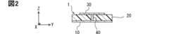
図1は、本実施形態に係るアンテナ装置1の概略的な構成の一例を示す外観斜視図である。図2は、図1に示すII-II線におけるアンテナ装置1の断面図である。アンテナ装置1は、例えば、車両などの移動体に搭載されて用いられる。 FIG. 1 is an external perspective view showing an example of a schematic configuration of an
このアンテナ装置1は、所定の対象周波数の電波を送受信するように構成されている。もちろん、他の態様としてアンテナ装置1は、送信と受信の何れか一方のみに利用されても良い。電波の送受信には可逆性があるため、或る周波数の電波を送信可能な構成は、当該周波数の電波を受信可能な構成でもある。 This
対象周波数は、ここでは一例として2.45GHzとする。もちろん、対象周波数は適宜設計されれば良く、他の態様として例えば300MHzや、760MHz、850MHz、900MHz、1.17GHz、1.28GHz、1.55GHz、5.9GHz等としてもよい。アンテナ装置1は、対象周波数だけでなく、対象周波数を基準として定まる所定範囲内の周波数の電波もまた送受信可能である。例えばアンテナ装置1は、2400MHzから2500MHzまでの帯域(以降、2.4GHz帯)に属する周波数を送受信可能に構成されている。 The target frequency is 2.45 GHz here as an example. Of course, the target frequency may be designed as appropriate, and may be, for example, 300 MHz, 760 MHz, 850 MHz, 900 MHz, 1.17 GHz, 1.28 GHz, 1.55 GHz, 5.9 GHz, etc. The
つまり、アンテナ装置1は、Bluetooth Low Energy(Bluetoothは登録商標)や、Wi-Fi(登録商標)、ZigBee(登録商標)等といった、近距離無線通信で使用される周波数帯の電波を送受信可能に構成されている。換言すれば、アンテナ装置1は、国際電気通信連合によって規定されている、産業・科学・医療分野で汎用的に使うために割り当てられた周波数の帯域(いわゆるISMバンド)の電波を送受信可能に構成されている。 In other words, the
以降における「λ」は、対象周波数の電波の波長(以降、対象波長とも記載)を表す。例えば「λ/2」及び「0.5λ」は対象波長の半分の長さを指し、「λ/4」及び「0.25λ」は対象波長の4分の1の長さを指す。なお、真空中及び空気中における2.4GHzの電波の波長(つまりλ)は125mmである。 Hereinafter, "λ" represents the wavelength of radio waves of the target frequency (hereinafter also referred to as target wavelength). For example, "λ/2" and "0.5λ" refer to a half length of the target wavelength, and "λ/4" and "0.25λ" refer to a quarter length of the target wavelength. Note that the wavelength (that is, λ) of a 2.4 GHz radio wave in vacuum and air is 125 mm.
アンテナ装置1は、例えばケーブルを介して、車両に搭載されている通信用のECU(Electronic Control Unit)と接続されており、アンテナ装置1が受信した信号は通信用ECUに逐次出力される。また、アンテナ装置1は通信用ECUから入力される電気信号を電波に変換して空間に放射する。通信用ECUは、アンテナ装置1が受信した信号を利用するとともに、当該アンテナ装置1に対して送信信号に応じた高周波電力を供給するものである。 The
ここでは一例としてアンテナ装置1と通信用ECUとは、AV線で接続する場合を想定して説明する。AV線は、自動車用低圧電線であって、軟銅より線を例えば塩化ビニルなどの絶縁材料で被覆することによって実現されている。AV線の「A」は自動車用低圧電線を指し、「V」はビニルを指す。アンテナ装置1に接続するAV線としては、接地電位を提供するためのAV線である接地用ケーブルと、信号が流れるAV線である信号用ケーブルとがある。なお、アンテナ装置1と通信用ECUとの接続ケーブルとしては、自動車用薄肉低圧電線(AVSSケーブル)や、自動車用圧縮導体超薄肉塩化ビニル絶縁低圧電線(CIVUSケーブル)なども採用可能である。AVSSの「SS」は極薄肉型を指す。CIVUSの「C」は圧縮導体型、「I」はISO規格、「V」はビニル、「US」は超極薄肉型を指す。また、アンテナ装置1と通信用ECUとを接続するケーブルとしては同軸ケーブルやフィーダ線など、その他の通信ケーブルを用いて接続しても良い。アンテナ装置1とケーブルとの接続点にはインピーダンス整合回路などが設けられていても良い。 Here, as an example, a case will be described assuming that the
以下、アンテナ装置1の具体的な構成について述べる。図1に示すようにアンテナ装置1は、地板10、支持板20、対向導体板30、及び短絡部40を備えている。便宜上以降では、地板10に対して対向導体板30が設けられている側を、アンテナ装置1にとっての上側として各部の説明を行う。つまり、地板10から対向導体板30に向かう方向がアンテナ装置1にとっての上方向に相当する。また、対向導体板30から地板10に向かう方向がアンテナ装置1にとっての下方向に相当する。 The specific configuration of the
地板10は、銅などの導体を素材とする板状の導体部材である。地板10は、支持板20の下側面に沿って設けられている。ここでの板状には金属箔のような薄膜状も含まれる。つまり、地板10はプリント配線板等の樹脂製の板の表面に電気メッキ等によってパターン形成されたものでもよい。また、地板10は、複数の導体層及び絶縁層を含む多層基板の内部に配置された導体層を用いて実現されていても良い。この地板10は、接地用ケーブル51と電気的に接続されて、アンテナ装置1におけるグランド電位(換言すれば接地電位)を提供する。地板10と接地用ケーブル51との接続点であるケーブル接続点11の位置については別途説明する。 The
地板10は、長方形状に形成されている。地板10の短辺の長さは、例えば、電気的に0.4λに相当する値に設定されている。また、地板10の長辺の長さは、電気的に1.2λに設定されている。ここでの電気的な長さとは、フリンジング電界や、誘電体による波長短縮効果などを考慮した、実効的な長さである。当該構成は、短手方向の長さが対象波長よりも短く、かつ、長手方向の長さは短手方向の2倍以上に設定されている長方形状の地板10に相当する。なお、地板10の短辺の長さは、0.6λや、0.8λなどであってもよい。地板10の短辺はλ/4よりも長ければよい。地板10の長手方向の長さは、短手方向よりも長ければよく、1.0λや、1.5λなどであってもよい。地板10の短辺と長辺の長さの比は、概ね1:2、1:3、1:4、2:3、2:5などとすることができる。なお、支持板20が比誘電率4.3の誘電体を用いて形成されている場合、地板10表面での波長は、支持板20としての誘電体の波長短縮効果によって60mm程度となる。故に、電気的に1.2λに相当する長さとは、72mmとなる。 The
図1等の種々の図に示すX軸は地板10の長手方向を、Y軸は地板10の短手方向を、Z軸は上下方向をそれぞれ表している。Y軸方向が所定方向に相当する。これらX軸、Y軸、及びZ軸を備える3次元座標系は、アンテナ装置1の構成を説明するための概念である。なお、他の態様として地板10が正方形状である場合には、任意の1辺に沿う方向をX軸とすることができる。 In various figures such as FIG. 1, the X axis represents the longitudinal direction of the
なお、地板10は、少なくとも対向導体板30よりも大きければよい。地板10の寸法は適宜変更可能である。地板10の1つの辺の長さは、電気的に1波長よりも小さい値(例えば対象波長の1/3)に設定されていても良い。また、地板10を上側から見た形状(以降、平面形状)は適宜変更可能である。ここでは一例として地板10の平面形状を長方形状とするが、他の態様として地板10の平面形状は、正方形状であってもよい。また、その他の多角形状であってもよい。例えば地板10は、1辺が電気的に1波長に相当する値に設定された正方形状であってもよい。矩形状には、長方形と正方形とが含まれる。 Note that the
支持板20は、地板10と対向導体板30とを、所定の間隔をおいて互いに対向配置するための板状部材である。支持板20は矩形平板状であり、支持板20の大きさは平面視において地板10とほぼ同じ大きさである。支持板20は、例えばガラスエポキシ樹脂など、所定の比誘電率を有する誘電体を用いて実現されている。ここでは一例として支持板20は比誘電率4.3のガラスエポキシ樹脂(換言すれば、FR4:Flame Retardant Type 4)を用いて実現されている。 The
本実施形態では一例として支持板20の厚さH1は、例えば1.5mmに形成されている。支持板20の厚さH1は、地板10と対向導体板30との間隔に相当する。支持板20の厚さH1を調整することで、対向導体板30と地板10との間隔を調整することができる。支持板20の厚さH1の具体的な値はシミュレーションや試験によって適宜決定されれば良い。もちろん、支持板20の厚さH1は、2.0mmや、3.0mmなどであってもよい。なお、支持板20での波長は、誘電体の波長短縮効果によって60mm程度となる。故に、厚さ1.5mmという値は、電気的に対象波長の40分の1(つまりλ/40)に相当する。 In this embodiment, the thickness H1 of the
なお、支持板20は前述の役割を果たせればよく、支持板20の形状は適宜変更可能である。対向導体板30を地板10に対向配置するための構成は、複数の柱であってもよい。また、本実施形態において地板10と対向導体板30の間は、支持板20としての樹脂が充填された構成を採用するが、これに限らない。地板10と対向導体板30の間は、中空や真空となっていてもよい。支持板20としては、ハニカム構造などを採用することもできる。さらに、以上で例示した構造が組み合わさっていてもよい。アンテナ装置1がプリント配線板を用いて実現される場合には、プリント配線板が備える複数の導体層を、地板10や、対向導体板30として利用するとともに、導体層を隔てる樹脂層を支持板20として利用してもよい。 Note that the
支持板20の厚さH1は、後述するように短絡部40の長さを調整するパラメータとしても機能する。換言すれば、支持板20の厚さH1は、短絡部40が提供するインダクタンスを調整するパラメータとして機能する。加えて厚さH1は、地板10と対向導体板30とが対向することによって形成される静電容量を調整するパラメータとしても機能する。 The thickness H1 of the
支持板20において対向導体板30が配置されている側の面(以降、支持板上側面20a)には、送受信回路70が形成されていてもよい。送受信回路70は、変調、復調、周波数変換、増幅、デジタルアナログ変換、及び検波の少なくとも何れか1つを実施する回路モジュールである。送受信回路70は、ICや、アナログ回路素子、コネクタなど、多様な部品の電気的集合体である。送受信回路70は、給電線路71としてのマイクロストリップなどで対向導体板30と電気的に接続されている。また、送受信回路70は、ビアまたは短絡ピン等を介して地板10とも接続されている。送受信回路70は、信号用ケーブルとしてのAV線とも電気的に接続されている。つまり、送受信回路70は信号用ケーブルを介して通信用ECUと接続されている。なお、アンテナ装置1における信号用ケーブルの接続箇所は任意の位置をすることができる。 The transmitting/receiving
対向導体板30は、銅などの導体を素材とする板状の導体部材である。ここでの板状には、前述の通り、銅箔などの薄膜状も含まれる。対向導体板30は、支持板20を介し、地板10と対向するように配置されている。対向導体板30もまた地板10と同様にプリント配線板等の、樹脂製の板の表面にパターン形成されたものでもよい。また、ここでの「平行」とは完全な平行状態に限らない。数度から30度程度傾いていても良い。つまり概ね平行である状態(いわゆる略平行な状態)を含みうる。本開示における「垂直」という表現についても、完全に垂直な状態に限らず、数度~30度程度傾いている態様も含まれる。 The
対向導体板30と地板10とは、互いに対向配置されることで、対向導体板30の面積や、対向導体板30と地板10との間隔に応じた静電容量を形成する。対向導体板30は、短絡部40が備えるインダクタンスと対象周波数において並列共振する静電容量を形成する大きさに形成されている。対向導体板30の面積は、所望の静電容量を提供するように適宜設計されればよい。所望の静電容量とは、短絡部40のインダクタンスとの協働により対象周波数で動作する静電容量である。なお、動作周波数をf、短絡部40が備えるインダクタンスをL、対向導体板30が地板10との間に形成する静電容量をCとすると、f=1/{2π√(LC)}の関係が成り立つ。当業者であれば、当該関係式をもとに、適正な対向導体板30の面積を決定することは可能である。 The opposing
例えば対向導体板30は、一辺が電気的に12mmmの正方形状に形成されている。対向導体板30の表面での波長は支持板20の波長短縮効果によって60mm程度となるため、12mmという値は、電気的に0.2λに相当する。もちろん、対向導体板30の一辺の長さは適宜変更可能であり、14mmや、15mm、20mm、25mmなどであっても良い。なお、対向導体板30の平面形状は、円形や、正八角形、正六角形などであってもよい。また、対向導体板30は、長方形状や長楕円形などであってもよい。 For example, the
対向導体板30には給電点31が形成されている。給電点31は給電線路71と対向導体板30とが電気的に接続される部分である。本構成において給電点31は、任意の位置に配置可能である。給電線路71とのインピーダンスの整合が取れる位置に設けられればよい。換言すれば給電点31は、リターンロスが所定の許容レベルとなる位置に設けられればよい。給電点31は、例えば対向導体板30の縁部や中央領域など、任意の位置に配置することができる。ここでは一例として対向導体板30の中心を通りかつX軸に平行な直線上に給電点31が形成されている。 A
なお、対向導体板30への給電方式としては、直結給電方式や電磁結合方式など多様な方式を採用可能である。直結給電方式は、給電線路71と対向導体板30とが直接接続される方式を指す。電磁結合方式は、給電用のマイクロストリップ線路等と対向導体板30との電磁結合を利用した給電方式を指す。 Note that as a method of feeding power to the opposing
短絡部40は、地板10と対向導体板30とを電気的に接続する導電性の部材である。短絡部40は、導電性のピン(以降、ショートピン)を用いて実現されれば良い。短絡部40としてのショートピンの径や長さを調整することによって、短絡部40が備えるインダクタンスを調整することができる。 The
なお、短絡部40は、一端が地板10と電気的に接続され、他端が対向導体板30と電気的に接続された線状の部材であればよい。アンテナ装置1がプリント配線板を基材として用いて実現される場合には、プリント配線板に設けられたビアを短絡部40として利用することができる。 Note that the
短絡部40は、例えば導体板中心に位置するように設けられている。なお、短絡部40の形成位置は、厳密に導体板中心と一致している必要はない。短絡部40は導体板中心から数mm程度ずれていてもよい。短絡部40は、対向導体板30の中央領域に形成されていれば良い。対向導体板30の中央領域とは、導体板中心から縁部までを1:5に内分する点を結ぶ線よりも内側の領域を指す。中央領域は、別の観点によれば、対向導体板30を6分の1程度に相似縮小した同心図形が重なる領域に相当する。 The
<地板10に対する対向導体板30の位置について>
対向導体板30は、図3に示すように、或る1組の対辺がX軸と平行となり、かつ、他の組の対辺がY軸に平行となる姿勢で地板10と対向配置されている。例えば、対向導体板30は、その中心が地板10の中心から所定のオフセット量ΔXだけX軸負方向にずれた位置に配置されている。オフセット量ΔXは例えば、0.125λ、0.25λ、0.5λなどとすることができる。対向導体板30は、地板10のX軸負方向(紙面左端)の端部に沿うように配置されていても良い。オフセット量ΔXは、上面視において対向導体板30が地板10の外側にはみ出さない範囲において適宜変更可能である。対向導体板30は、少なくとも全領域(換言すれば全面)が地板10と対向するように配置されている。オフセット量ΔXは、地板10の中心と対向導体板30の中心のずれ量に相当する。<About the position of the
As shown in FIG. 3, the
なお、図3では地板10と対向導体板30の位置関係を明示するために、支持板20及び送受信回路70等は透過させている。つまり図示を省略している。図3に示す一点鎖線Lx1は、地板10の中心を通ってX軸に平行な直線を表しており、一点鎖線Ly1は、地板10の中心を通ってY軸に平行な直線を表している。二点鎖線Ly2は、対向導体板30の中心を通ってY軸に平行な直線を表す。直線Lx1は、別の観点によれば、地板10や対向導体板30にとっての対称軸に相当する。直線Ly1は地板10にとっての対称軸に相当する。直線Ly2は対向導体板30にとっての対称軸に相当する。一点鎖線Lx1は、対向導体板30の中心も通る。つまり、一点鎖線Lx1は、X軸に平行な直線であって地板10と対向導体板30の中心を通る直線に相当する。直線Lx1と直線Ly1との交点が地板中心に相当し、直線Lx1と直線Ly2の交点が対向導体板30の中心(以降、導体板中心)に相当する。導体板中心は、対向導体板30の重心に相当する。本実施形態では対向導体板30が正方形状であるため、導体板中心とは、対向導体板30の2つの対角線の交点に相当する。なお、地板10と対向導体板30とが同心となる配置態様とは、上面視において対向導体板30の中心と地板10の中心とが重なる配置態様に相当する。 In addition, in FIG. 3, in order to clearly show the positional relationship between the
<アンテナ装置1の動作原理について>
ここではアンテナ装置1の動作を説明する。アンテナ装置1は、対向導体板30はその中央領域に設けられた短絡部40で地板10に短絡されており、かつ、対向導体板30の面積は、短絡部40が備えるインダクタンスと対象周波数において並列共振する静電容量を形成する面積となっている。<About the operating principle of the
Here, the operation of the
このため、送受信回路70から高周波信号が入力されると、インダクタンスと静電容量との間のエネルギー交換によってLC並列共振が生じ、地板10と対向導体板30との間には、地板10および対向導体板30に対して垂直な電界が発生する。この垂直電界は、短絡部40から対向導体板30の縁部に向かって伝搬していき、対向導体板30の縁部において、垂直電界は地板10に垂直な偏波面を持つ直線偏波(以降、地板垂直偏波)になって空間を伝搬していく。つまり、短絡部40及び対向導体板30を含む構成が、放射素子、換言すればアンテナ素子2として機能する。なお、ここでの地板垂直偏波とは、電界の振動方向が地板10や対向導体板30に対して垂直な電波を指す。 Therefore, when a high frequency signal is input from the transmitting/receiving
また、アンテナ装置1は対象周波数において、アンテナ水平方向に指向性を有する。故に、地板10が水平となるように配置されている場合、アンテナ装置1は水平方向にメインビームを備えるアンテナとして機能する。ここでのアンテナ水平方向とは、対向導体板30の中心からその縁部に向かう方向を指す。アンテナ水平方向は、別の観点によれば、対向導体板30の中心を通る地板10への垂線に直交する方向を指す。アンテナ水平方向は、アンテナ装置1にとっての横方向(換言すれば側方)に相当する。 Further, the
なお、アンテナ装置1が電波を送信(放射)する際の作動と、電波を受信する際の作動は、互いに可逆性を有する。つまり上記アンテナ装置1によれば、アンテナ水平方向から到来する地板垂直偏波を受信できる。 Note that the operation when the
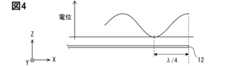
<地板10におけるケーブル接続点11の位置について>
本開示において接地用ケーブル51と地板10との接続点であるケーブル接続点11は、地板10のX軸正方向の端部(図面上の右端)からの距離αがλ/4となる位置に配置されている。具体的には、地板10の中心を通ってX軸に平行な直線Lx1上において、アンテナ素子2としての対向導体板30が配置されていない方の端部(以降、アンテナ遠方端12)から、λ/4離れた位置に設けられている。以降では便宜上、アンテナ遠方端12からλ/4離れた地板10の部分をλ/4地点とも記載する。<About the position of the
In the present disclosure, the
なお、地板10のX軸正方向の端部からの距離がλ/4の3倍や5倍となる位置に配置されていてもよい。ケーブル接続点11は、地板10の端部からの距離αがλ/4×N(Nは奇数)となる位置に設けられていればよい。また、ケーブル接続点11は、アンテナ遠方端12からλ/4の奇数倍離れた位置に配置されていればよく、Y方向の位置は、直線Lx1上に限定されない。図3に示す位置からY軸正又は負方向にずれた位置に配置されていても良い。 Note that it may be arranged at a position where the distance from the end of the
接地用ケーブル51はケーブル接続点11からY軸に平行な姿勢で配線されるか、地板10からλ/20以上離れて配線されることが好ましい。そのような構成によればケーブル接続点11以外において接地用ケーブル51が地板10と電気的或いは電磁気的に結合することを抑制することができる。 It is preferable that the
<作用効果>
シミュレーションの結果、LC並列共振によって地板10に流れる電流は、主として、短絡部40から地板10の縁部に向かって流れることが確認されている。また、対向導体板30から短絡部40を通って地板10に流れ込んだ電流は、短絡部40から地板10の長手方向の両側に流れる。つまり、地板10に流れる電流は、短絡部40からアンテナ遠方端12に向かって流れる。<Effect>
As a result of simulation, it has been confirmed that the current flowing through the
ここで、アンテナ遠方端12では電流はゼロとなることから、図4に示すように、アンテナ遠方端12での電位は最大となり、アンテナ遠方端12からλ/4×Nの位置では電位は最小となる。電位が最小となる点においては、導体が近接しても地板10の電位は変化しない。故に、電位が最小となる点においては、導体が近接しても電流の変化も生じないことなる。そのため、アンテナ遠方端12からλ/4の奇数倍となる位置にケーブル接続点11を設けた構成によれば、地板10から接地用ケーブル51への漏洩電流を抑制することが可能となる。 Here, since the current is zero at the antenna
図5及び図6は、ケーブル接続点11をアンテナ遠方端12からλ/2離れた位置に設けた場合と、λ/4離れた位置に設けた場合の、接地用ケーブル51の有無による指向性変化を解析した結果である。図5が、ケーブル接続点11をアンテナ遠方端12からλ/2離れた位置に設けた場合を示しており、図6が、ケーブル接続点11をアンテナ遠方端12からλ/4離れた位置に設けた場合を示している。図5、図6における破線は接地用ケーブル51が存在しない場合の指向性のシミュレーション結果を示しており、実線は、接地用ケーブル51が存在する場合の指向性のシミュレーション結果を示している。つまり、図5及び図6における破線と実線とのギャップは、接地用ケーブル51による指向性への影響度合いを示している。図5及び図6を比較すれば明らかなように、ケーブル接続点11の位置をλ/4離した位置に設けた構成によれば、接地用ケーブル51による指向性の乱れを抑制できる。なお、指向性の乱れは、接地用ケーブル51への漏洩電流に由来する。つまり、図5及び図6は、ケーブル接続点11の位置をλ/4離した位置に設けた構成によれば、接地用ケーブル51への漏洩電流を抑制できることを間接的に示している。 5 and 6 show the directivity depending on the presence or absence of the
以上で述べたように上記構成によれば、地板10のサイズが対象波長に対して不十分である場合であっても、接地用ケーブル51への電流の漏洩量を低減できる。上記の地板10に対するケーブルの接続方法は、地板10の短手方向の長さが0.75λ未満となっている構成において特に好適に作用する。また、地板10が長手方向を有する長方形であって、長手方向の一方の端部にアンテナ素子2が配置されている構成において、特に好適である。長手方向の一方の端部にアンテナ素子2が配置されている構成においては、反対側の端部であるアンテナ遠方端12に向かって電流が流れ、電圧分布の腹と節が形成されやすいためである。 As described above, according to the above configuration, even if the size of the
上記のアンテナ装置1は、対向導体板30及び短絡部40を含むアンテナ素子2がLC並列共振することにより、アンテナ水平方向に地板垂直偏波を送受信できる。なお、地板垂直偏波を送受信可能な他の構成としては、アンテナ素子2としてモノポールアンテナを採用することもできる。ただし、アンテナ素子2をモノポールアンテナとする構成では、λ/4の高さが必要になってしまう。これに対し、上記アンテナ装置1ではλ/100程度の高さ(換言すれば厚さ)で実現可能である。つまり、上記開示の構成によれば、アンテナ装置1の高さを抑制できる。 The
加えて、ケーブル接続点11の位置をλ/4の奇数倍となる位置に配置することにより、ローパスフィルタ等の回路素子を設けることなく、接地用ケーブル51への漏洩電流を抑制できる。つまり、製造コストの抑制とアンテナ特性の安定化を両立することができる。 In addition, by arranging the
<アンテナ装置1の使用方法について>
上述したアンテナ装置1は、例えば図7に示すように、車両のBピラー91の車室外側の面に、地板10がBピラー91の表面と対向し、かつ、X軸方向がBピラー91の長手方向(換言すれば車両高さ方向)に沿う姿勢で取り付け使用されればよい。あるいは、ドアパネル内部においてBピラー91と重なる部分に、上記の姿勢にて取り付けられていても良い。<How to use the
For example, as shown in FIG. 7, the
以上の取り付け姿勢によれば、アンテナ装置1にとっての上方向であるZ軸正方向が、車幅方向に略一致し、アンテナ水平方向は、車両側面部に沿う(換言すれば平行な)方向となる。当該取り付け姿勢によれば、車両側面部に沿うように通信エリアを形成する事ができる。 According to the above mounting posture, the positive Z-axis direction, which is the upward direction for the
なお、アンテナ装置1の取付位置及び取付姿勢は上記の例に限定されない。アンテナ装置1は、Aピラー92やCピラーの車室外側の面、ロッカー部(換言すればサイドシル)94、アウタードアハンドル95の内部/付近など、車両外面部の任意の位置に取り付けることができる。例えば、アンテナ装置1は、アウタードアハンドル95の内部に、X軸方向がハンドルの長手方向に沿い、かつ、Y軸が車両高さ方向に沿う姿勢で収容されていても良い。また、アンテナ装置1はルーフ部93に搭載されても良い。 Note that the mounting position and mounting posture of the
以上、本開示の実施形態を説明したが、本開示は上述の第1実施形態に限定されるものではなく、以降で述べる種々の補足や変形例も本開示の技術的範囲に含まれる。さらに、下記以外にも要旨を逸脱しない範囲内で種々変更して実施することができる。例えば下記の種々の変形例は、技術的な矛盾が生じない範囲において適宜組み合わせて実施することができる。 Although the embodiments of the present disclosure have been described above, the present disclosure is not limited to the first embodiment described above, and various supplements and modifications described below are also included within the technical scope of the present disclosure. Furthermore, various modifications other than those described below can be made without departing from the scope of the invention. For example, the various modifications described below can be implemented in appropriate combinations within a range that does not cause technical contradiction.
<アンテナ素子2について>
上述した実施形態では、アンテナ装置1は、対向導体板30と短絡部40を含む構成をアンテナ素子2として備える構成を開示した。換言すれば、アンテナ素子2として0次共振アンテナを用いた構成を開示したがこれに限らない。アンテナ素子2は、モノポールアンテナであってもよいし、パッチアンテナであってもよい。アンテナ素子2は、逆Fアンテナ又はループアンテナであってもよい。アンテナ装置1のアンテナ素子2としては多様なアンテナ構成を採用可能である。<About
In the embodiment described above, the
<地板10に対する接地用ケーブル51の接続態様について>
ケーブル接続点11において接地用ケーブル51は、図8に示すようにコネクタ52を用いて地板10に垂直に接続されていても良い。このような構成によれば接地用ケーブル51と地板10とがケーブル接続点11以外において電気的または電磁気的に結合する恐れを低減できる。<About the connection mode of the
At the
また、他の態様としては図9に示すように、アンテナ遠方端12からλ/4地点に向かって幅Wのスリット13を設け、当該スリット13の中心線上を通るように接地用ケーブル51を配線しても良い。接地用ケーブル51がスリット13の奥側端部で地板10と接続される。ここでの奥側とは、スリット13の延設方向のうち、アンテナ遠方端12から反対側の端部に向かう方向を指す。図8に示す接続構成では、コネクタ52が地板10に対して垂直な姿勢で接続するため、アンテナ装置1全体の高さがコネクタ52の分だけ高くなってしまう。これに対して、図9に示す構成によれば、コネクタ52が地板10に対して平行に接続するため、アンテナ装置1の高さを抑制可能となる。つまり、Bピラー91等の搭載スペースの厚みが少ない場所への搭載性を高めることができる。なお、幅Wは、スリット13の中心を通る接地用ケーブル51と地板10とが電磁気的に結合しない程度の幅となっていればよく、例えば、幅Wはλ/10以上とすることできる。当該構成によれば、接地用ケーブル51と地板10とのY軸方向の間隔は概ねλ/20以上となり、電磁気的な結合を抑制可能となる。 In addition, as another aspect, as shown in FIG. 9, a
なお、地板10の下側には支持板20に相当する絶縁層が形成されていても良い。つまり、地板10はプリント基板の内層を用いて実現されていても良い。地板10をプリント多層基板の内層を用いて実現する構成においては、コネクタ52をスリット13の奥側端部に取り付けることは難しい。そこで、図10に示すように、λ/4地点11aから、アンテナ遠方端12まで、スリット13の中心を通る導電線路(以降、引出し線路14)を形成し、引出し線路14の端部に接地用ケーブル51を接続しても良い。引出し線路14は、例えばパターン形成された配線に相当する。引出し線路14はマイクロストリップまたはストリップラインとして形成されていても良い。そのような構成によればアンテナ遠方端12にコネクタ52を配置しつつも実質的な接続点は、λ/4地点とすることができる。当該構成は、引出し線路14に対して接地用ケーブル51が直列的に接続することにより、接地用ケーブル51が引出し線路14を介して地板10と電気的に接続する構成に相当する。引出し線路14は、地板10の上側及び下側の少なくとも何れか一方に形成された、支持板20としての絶縁層に付着されていれば良い。アンテナ装置1が複数の導体層及び絶縁層を含む多層基板を用いて構成される場合、通信用ケーブルは、地板10としての導体層とは別の導体層の任意の箇所で電気的に接続可能である。 Note that an insulating layer corresponding to the
<地板10及び対向導体板30の形状及び位置関係の補足>
地板10は概略的に矩形状であればよく、角部が丸められていてもよい。また、地板10の縁部は、部分的に又は全体的にミアンダ形状に形成されていても良い。矩形状には、その縁部に微小な凹凸が設けられている形状も含まれる。地板10の縁部に設けられた凹凸や、地板10の縁部から離れた位置に形成されているスリットは、アンテナ動作に影響を与えない限りにおいては、地板10の外観形状を定義する上で無視することができる。ここでの微小な凹凸とは数mm程度の凹凸を指す。<Supplementary information on the shape and positional relationship of the
The
対向導体板30には、スリットが設けられたり、角部を丸められたりしていても良い。例えば1対の対角部分に縮退分離素子としての切り欠き部が設けられていてもよい。対向導体板30の縁部は、部分的に又は全体的にミアンダ形状に設定されていても良い。対向導体板30の縁部に設けられた、動作に影響を与えない程度の凹凸は無視して取り扱うことができる。 The
また、地板10の形状や、地板10に対する対向導体板30の配置態様は、実施形態として開示した構成に限定されない。地板10に対する対向導体板30の配置態様としては、図11~図13に例示するように多様な配置態様を採用することができる。例えば図11に示すように、対向導体板30は、X軸負方向側の端部が地板10のX軸負方向側の端部と揃うように配置されていても良い。図11~図13では地板10と対向導体板30の位置関係を明示するために、支持板20及び送受信回路70等の図示を省略している。各図の寸法は一例であって適宜変更可能である。 Furthermore, the shape of the
なお、図12に示すLx2は、対向導体板30の中心を通ってX軸に平行な直線を示している。また、図12のΔXは、地板10に対する対向導体板30のX軸方向のオフセット量を表しており、ΔYはY軸方向のオフセット量を表している。ΔXとΔYは同じ値であってもよいし、異なる値であっても良い。図12に開示の構成は、対向導体板30を地板10と同心となる位置からX軸方向及びY軸方向に所定量ずらして配置した構成に相当する。 Note that Lx2 shown in FIG. 12 indicates a straight line passing through the center of the opposing
また、ケーブル接続点11を設ける際の基準とする地板10の端部は、長手方向の端部に限らない。図13に示すように短手方向の端部のうち、相対的に短絡部40から離れている方の端部からλ/4の奇数倍離れた位置に設けられていても良い。 Further, the end portion of the
<アンテナ装置1全体構成の補足>
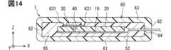
アンテナ装置1は、図14に示すように、対向導体板30、短絡部40が形成されている支持板20を収容するケース60を備えていても良い。なお、図14はケース60内部の構成を概念的に示す図である。図の視認性確保のため、材料種別を示すハッチング等は省略している。ケース60は例えば上下方向に分離可能に構成されているアッパーケースとロアケースとが組み合わさることで構成されている。ケース60は、例えばポリカーボネート(PC:polycarbonate)樹脂を用いて構成されている。なお、ケース60の材料としては、PC樹脂にアクリロニトリルブタジエンスチレン共重合体(いわゆるABS)を混ぜた合成樹脂や、ポリプロピレン(PP:polypropylene)など、多様な樹脂を採用できる。ケース60は、ケース底部61、側壁部62、及びケース天板部63を備える。ケース底部61は、ケース60の底を提供する構成である。ケース底部61は、平板状に形成されている。ケース60内において、地板10や対向導体板30、送受信回路70などを含む回路基板は、地板10がケース底部61と対向するように配置されている。<Supplementary information on the overall configuration of
As shown in FIG. 14, the
側壁部62は、ケース60の側面を提供する構成であって、ケース底部61の縁部から上方に向かって立設されている。側壁部62の高さは、例えば、ケース天板部63の内面と対向導体板30との離隔がλ/25以下となるように設計されている。ケース天板部63は、ケース60の上面部を提供する構成である。本実施形態のケース天板部63は平板状に形成されている。なお、ケース天板部63の形状としては、その他、ドーム型など多様な形状を採用することができる。ケース天板部63は、内面が支持板上側面20aと対向するように構成されている。側壁部62には、接地用ケーブル51等を引き出すための穴であるケーブル引出し部64が設けられている。ケーブル引出し部64を側壁部62に設けた構成によれば、Bピラー91等への搭載性を高めることができる。 The
上記構成のようにケース天板部63が対向導体板30の近くに存在する場合には、LC共振モードによって放射される垂直電界が、対向導体板30の縁部から上側に回り込むことを抑制し、アンテナ水平方向への放射利得を高めることができる。ここでの対向導体板30の近くとは、例えば対向導体板30からの距離が電気的に対象波長の25分の1以下となる領域を指す。 When the case
加えて、ケース天板部63には、図14に示すように、対向導体板30の縁部と当接する上側リブ631が形成されていても良い。上側リブ631は、ケース天板部63の内側面に、下方向かって形成された凸状の構成である。上側リブ631は、対向導体板30の縁部と当接するように設けられている。上側リブ631は、ケース60内における支持板20の位置を固定するとともに、対向導体板30の端部から上側への地板垂直偏波の回り込みを抑制し、アンテナ水平方向への放射利得を向上させる効果を奏する。上側リブ631において対向導体板30の縁部と連接する垂直面(つまり外側面)には、銅箔等の金属パターンが付与されていても良い。 In addition, the case
加えて、ケース60の内部には、シリコン等のシール材65を充填されていることが好ましい。シール材65としてはポリウレタンプレポリマーなど、ウレタン樹脂を採用することができる。もちろん、シール材65としては、その他、エポキシ樹脂やシリコン樹脂など多様な材料を採用することができる。ケース60内にシール材65を充填した構成によれば、対向導体板30の上方に位置するシール材65が、対向導体板30の端部から上側への地板垂直偏波の回り込みを抑制し、アンテナ水平方向への放射利得を向上させる効果を奏する。ケース60は、少なくとも側面部及び上面部が所定の比誘電率を有する樹脂又はセラミックにて形成されていれば良い。また、ケース60内にシール材65を充填した構成によれば、防水性や防塵性、耐振動性も向上させる事ができる。 In addition, the inside of the
もちろん、ケース60内におけるシール材65の充填は任意の要素である。上側リブ631もまた任意の要素である。なお、ケース天板部63や上側リブ631、シール材65は、LC共振モードによって放射される垂直電界が、対向導体板30の縁部から上側に回り込むことを抑制する役割を担う構成(以降、電波遮断体)に相当する。上記構成は、対向導体板30の上側に、導体又は誘電体を用いて構成されている電波遮断体を配置した構成に相当する。 Of course, filling the sealing
ケース60が備えるケース底部61及びケース天板部63の何れか一方は省略されていても良い。ケース底部61及びケース天板部63の何れか一方が省略される場合、シール材65はアンテナ装置1が使用される環境の温度として想定される範囲(以降、使用温度範囲)において固形を維持する樹脂を用いて実現されていることが好ましい。使用温度範囲は例えば-30℃~100℃とすることができる。なお、ケース底部61及びケース天板部63の何れか一方が省略された構成は、ケースの上面又は底面を開口部としたケースとなる。 Either one of the case
1 アンテナ装置、2 アンテナ素子、10 地板、11 ケーブル接続点、12 アンテナ遠方端、13 スリット、14 引出し線路(導電線路)、20 支持板、30 対向導体板、31 給電点、40 短絡部、51 接地用ケーブル、52 コネクタ、60 ケース、61 ケース底部、62 ケース側壁部、63 ケース天板部、631 上側リブ、65 シール材、70 送受信回路、71 給電線路 1 antenna device, 2 antenna element, 10 ground plate, 11 cable connection point, 12 antenna far end, 13 slit, 14 lead line (conductive line), 20 support plate, 30 opposing conductor plate, 31 feeding point, 40 short circuit part, 51 Grounding cable, 52 Connector, 60 Case, 61 Case bottom, 62 Case side wall, 63 Case top plate, 631 Upper rib, 65 Sealing material, 70 Transmission/reception circuit, 71 Power supply line
Claims (10)
Translated fromJapanese給電線と電気的に接続する給電点が設けられている導体部材であるアンテナ素子(2)と、を備え、
前記地板の所定方向の長さは送受信の対象とする電波の波長である対象波長よりも短く設定されており、
前記地板には、前記地板の縁部からの距離が前記対象波長の4分の1の奇数倍となる位置に、接地用ケーブルが接続されており、
前記地板には前記縁部から長手方向に沿って前記対象波長の4分の1の奇数倍の長さのスリット(13)が形成されており、
前記接地用ケーブルは、前記スリットの奥側端部と電気的に接続されているアンテナ装置。a base plate (10) that is a flat conductor member formed in a rectangular shape;
An antenna element (2) that is a conductive member provided with a feeding point electrically connected to the feeding line,
The length of the ground plate in a predetermined direction is set shorter than a target wavelength that is a wavelength of radio waves to be transmitted and received,
A grounding cableis connected to the ground plate at a position where the distance from the edge of the ground plate is an odd multiple of a quarter of the target wavelength,
A slit (13) having a length that is an odd number multiple of a quarter of the target wavelength is formed in the base plate along the longitudinal direction from the edge,
The grounding cable is an antenna device electrically connected to a back end of the slit .
前記地板は、短手方向の長さが前記対象波長よりも短い長方形状であって、長手方向の長さは短手方向の2倍以上に設定されており、
前記アンテナ素子は、前記地板の中心と重なる位置から前記地板の長手方向にずれた位置に配置されており、
前記地板の長手方向の端部のうち、前記アンテナ素子から離れている方の端部であるアンテナ遠方端(12)からの距離が前記対象波長の4分の1の奇数倍となる位置に前記接地用ケーブルが接続されている、アンテナ装置。The antenna device accordingto claim 1 ,
The base plate has a rectangular shape with a length in the transverse direction shorter than the target wavelength, and the length in the longitudinal direction is set to be at least twice the length in the transverse direction,
The antenna element is arranged at a position shifted in the longitudinal direction of the ground plate from a position overlapping the center of the ground plate,
Among the longitudinal ends of the ground plate, the distance from the antenna far end (12), which is the end remote from the antenna element, is an odd multiple of one-fourth of the target wavelength. An antenna device to which a grounding cable is connected.
給電線と電気的に接続する給電点が設けられている導体部材であるアンテナ素子(2)と、を備え、
前記地板は、短手方向の長さが送受信の対象とする電波の波長である対象波長よりも短い長方形状であって、長手方向の長さは短手方向の2倍以上に設定されており、
前記アンテナ素子は、前記地板の中心と重なる位置から前記地板の長手方向にずれた位置に配置されており、
前記地板において、前記地板の長手方向の端部のうち前記アンテナ素子から離れている方の端部であるアンテナ遠方端(12)からの距離が前記対象波長の4分の1の奇数倍となる位置に、接地用ケーブルが接続されているアンテナ装置。a base plate (10) that is a flat conductor member formed in a rectangular shape;
An antenna element (2) that is a conductive member provided with a feeding point electrically connected to the feeding line,
The base plate has a rectangular shape in which the lengthinthe transverse directionis shorter than the target wavelength, which is the wavelength of the radio waves to be transmitted and received, and the length in the longitudinal direction is set to be at least twice the length in the transverse direction. Ori,
The antenna element is arranged at a position shifted in the longitudinal direction of the ground plate from a position overlapping the center of the ground plate,
In the ground plate, the distance from the antenna far end (12), which is the end of the longitudinal direction of the ground plate that is remote from the antenna element, is an odd multiple of one-fourth of the target wavelength. An antenna device to which a grounding cable is connected.
給電線と電気的に接続する給電点が設けられている導体部材であるアンテナ素子(2)と、を備え、
前記地板は、短手方向の長さが送受信の対象とする電波の波長である対象波長よりも短い長方形状であって、長手方向の長さは短手方向の2倍以上に設定されており、
前記アンテナ素子は、前記地板の中心と重なる位置から前記地板の長手方向にずれた位置に配置されており、
前記地板の長手方向の端部のうち、前記アンテナ素子から離れている方の端部であるアンテナ遠方端(12)から、反対側の端部に向かって前記対象波長の4分の1の奇数倍の長さのスリット(13)が形成されており、
前記スリットの中心線上には、導電線路(14)が形成されており、
前記地板には、前記導電線路を介して接地用ケーブルが直列的に接続されているアンテナ装置。a base plate (10) that is a flat conductor member formed in a rectangular shape;
An antenna element (2) that is a conductive member provided with a feeding point electrically connected to the feeding line,
The base plate has a rectangular shape in which the length in the transverse direction is shorter than the target wavelength, which is the wavelength of the radio waves to be transmitted and received, and the length in the longitudinal direction is set to be at least twice the length in the transverse direction. ,
The antenna element is arranged at a position shifted in the longitudinal direction of the ground plate from a position overlapping the center of the ground plate,
Among the longitudinal ends of the ground plate, from the antenna far end (12), which is the end remote from the antenna element, toward the opposite end, an odd number of 1/4 of the target wavelength. A slit (13) with twice the length is formed,
A conductive line (14) is formed on the center line of the slit,
In the antenna device, a grounding cable is connected in series to the ground plate via the conductive line.
前記アンテナ素子は、前記地板の長手方向の一方の端部に配置されているアンテナ装置。The antenna device according to any one of claims 1 to4 ,
In the antenna device, the antenna element is arranged at one longitudinal end of the ground plane.
給電線と電気的に接続する給電点が設けられている導体部材であるアンテナ素子(2)と、を備え、
前記地板の所定方向の長さは送受信の対象とする電波の波長である対象波長よりも短く設定されており、
前記地板には、前記地板の縁部からの距離が前記対象波長の4分の1の奇数倍となる位置に、接地用ケーブルが接続されており、
前記アンテナ素子は、前記地板の長手方向の一方の端部に配置されているアンテナ装置。a base plate (10) that is a flat conductor member formed in a rectangular shape;
An antenna element (2) that is a conductive member provided with a feeding point electrically connected to the feeding line,
The length of the ground plate in a predetermined direction is set shorter than a target wavelength that is a wavelength of radio waves to be transmitted and received,
A grounding cableis connected to the ground plate at a position where the distance from the edge of the ground plate is an odd multiple of a quarter of the target wavelength,
In the antenna device, the antenna element is arranged at one longitudinal end of the ground plane .
前記アンテナ素子は、
前記地板と所定の間隔をおいて設置された平板状の導体部材であって、前記給電点が設けられている対向導体板(30)と、
前記対向導体板の中央領域に設けられてあって、前記対向導体板と前記地板とを電気的に接続する短絡部(40)と、を用いて構成されており、
前記短絡部が備えるインダクタンスと、前記地板と前記対向導体板とが形成する静電容量とを用いて、所定の対象周波数で並列共振するように構成されている、アンテナ装置。The antenna device according to any one of claims 1 to 6,
The antenna element is
an opposite conductor plate (30), which is a flat conductor member installed at a predetermined distance from the ground plane, and on which the feed point is provided;
A shorting portion (40) is provided in the central region of the opposing conductor plate and electrically connects the opposing conductor plate and the ground plane,
An antenna device configured to resonate in parallel at a predetermined target frequency using an inductance provided in the short circuit portion and a capacitance formed by the ground plate and the opposing conductor plate.
給電線と電気的に接続する給電点が設けられている導体部材であるアンテナ素子(2)と、を備え、
前記地板の所定方向の長さは送受信の対象とする電波の波長である対象波長よりも短く設定されており、
前記地板には、前記地板の縁部からの距離が前記対象波長の4分の1の奇数倍となる位置に、接地用ケーブルが接続されており、
前記アンテナ素子は、
前記地板と所定の間隔をおいて設置された平板状の導体部材であって、前記給電点が設けられている対向導体板(30)と、
前記対向導体板の中央領域に設けられてあって、前記対向導体板と前記地板とを電気的に接続する短絡部(40)と、を用いて構成されており、
前記短絡部が備えるインダクタンスと、前記地板と前記対向導体板とが形成する静電容量とを用いて、所定の対象周波数で並列共振するように構成されているアンテナ装置。a base plate (10) that is a flat conductor member formed in a rectangular shape;
An antenna element (2) that is a conductive member provided with a feeding point electrically connected to the feeding line,
The length of the ground plate in a predetermined direction is set shorter than a target wavelength that is a wavelength of radio waves to be transmitted and received,
A grounding cableis connected to the ground plate at a position where the distance from the edge of the ground plate is an odd multiple of a quarter of the target wavelength,
The antenna element is
an opposite conductor plate (30), which is a flat conductor member installed at a predetermined distance from the ground plane, and on which the feed point is provided;
A shorting portion (40) is provided in the central region of the opposing conductor plate and electrically connects the opposing conductor plate and the ground plane,
An antenna deviceconfigured to resonate in parallel at a predetermined target frequency using an inductance provided in the short circuit portion and a capacitance formed by the ground plate and the opposing conductor plate.
前記アンテナ素子は、モノポールアンテナ、パッチアンテナ、逆Fアンテナ、及び、ループアンテナの何れかである、アンテナ装置。The antenna device according to any one of claims 1 to 6,
The antenna device is an antenna device in which the antenna element is any one of a monopole antenna, a patch antenna, an inverted F antenna, and a loop antenna.
前記接地用ケーブルは、前記地板に対して垂直に接続されている、アンテナ装置。The antenna device according toany one of claims 3 and 5 to 8 ,
In the antenna device, the grounding cable is connected perpendicularly to the ground plane.
Priority Applications (4)
| Application Number | Priority Date | Filing Date | Title |
|---|---|---|---|
| JP2020110670AJP7415820B2 (en) | 2020-06-26 | 2020-06-26 | antenna device |
| PCT/JP2021/023456WO2021261455A1 (en) | 2020-06-26 | 2021-06-21 | Antenna device |
| CN202180044935.8ACN115735302A (en) | 2020-06-26 | 2021-06-21 | Antenna device |
| US18/070,277US12261379B2 (en) | 2020-06-26 | 2022-11-28 | Antenna device |
Applications Claiming Priority (1)
| Application Number | Priority Date | Filing Date | Title |
|---|---|---|---|
| JP2020110670AJP7415820B2 (en) | 2020-06-26 | 2020-06-26 | antenna device |
Publications (3)
| Publication Number | Publication Date |
|---|---|
| JP2022007598A JP2022007598A (en) | 2022-01-13 |
| JP2022007598A5 JP2022007598A5 (en) | 2022-08-17 |
| JP7415820B2true JP7415820B2 (en) | 2024-01-17 |
Family
ID=79281168
Family Applications (1)
| Application Number | Title | Priority Date | Filing Date |
|---|---|---|---|
| JP2020110670AActiveJP7415820B2 (en) | 2020-06-26 | 2020-06-26 | antenna device |
Country Status (4)
| Country | Link |
|---|---|
| US (1) | US12261379B2 (en) |
| JP (1) | JP7415820B2 (en) |
| CN (1) | CN115735302A (en) |
| WO (1) | WO2021261455A1 (en) |
Citations (4)
| Publication number | Priority date | Publication date | Assignee | Title |
|---|---|---|---|---|
| US6421016B1 (en) | 2000-10-23 | 2002-07-16 | Motorola, Inc. | Antenna system with channeled RF currents |
| JP2010028500A (en) | 2008-07-22 | 2010-02-04 | Sony Corp | Radio communication circuit and radio communication apparatus |
| US20170012352A1 (en) | 2015-07-09 | 2017-01-12 | Quanta Computer Inc. | Communication device |
| WO2020195110A1 (en) | 2019-03-26 | 2020-10-01 | 株式会社Soken | Antenna device |
Family Cites Families (8)
| Publication number | Priority date | Publication date | Assignee | Title |
|---|---|---|---|---|
| BR9915453A (en)* | 1998-11-17 | 2001-10-16 | Xertex Technologies Inc | Broadband antenna with radiator / unit ground plan |
| JP4137724B2 (en) | 2003-07-04 | 2008-08-20 | 株式会社東芝 | ANTENNA DEVICE AND RADIO DEVICE |
| JP2007013643A (en)* | 2005-06-30 | 2007-01-18 | Lenovo Singapore Pte Ltd | Integrally formed flat-plate multi-element antenna and electronic apparatus |
| US7612725B2 (en)* | 2007-06-21 | 2009-11-03 | Apple Inc. | Antennas for handheld electronic devices with conductive bezels |
| JP4992762B2 (en) | 2008-02-29 | 2012-08-08 | 株式会社デンソー | Automotive integrated antenna |
| JP5341611B2 (en) | 2009-05-13 | 2013-11-13 | 株式会社東海理化電機製作所 | Antenna device |
| US9595755B2 (en)* | 2013-10-04 | 2017-03-14 | Laird Technologies, Inc. | Ground independent multi-band antenna assemblies |
| US10629987B2 (en)* | 2017-10-31 | 2020-04-21 | Avx Antenna, Inc. | Microstrip antenna assembly having a detuning resistant and electrically small ground plane |
- 2020
- 2020-06-26JPJP2020110670Apatent/JP7415820B2/enactiveActive
- 2021
- 2021-06-21WOPCT/JP2021/023456patent/WO2021261455A1/ennot_activeCeased
- 2021-06-21CNCN202180044935.8Apatent/CN115735302A/enactivePending
- 2022
- 2022-11-28USUS18/070,277patent/US12261379B2/enactiveActive
Patent Citations (4)
| Publication number | Priority date | Publication date | Assignee | Title |
|---|---|---|---|---|
| US6421016B1 (en) | 2000-10-23 | 2002-07-16 | Motorola, Inc. | Antenna system with channeled RF currents |
| JP2010028500A (en) | 2008-07-22 | 2010-02-04 | Sony Corp | Radio communication circuit and radio communication apparatus |
| US20170012352A1 (en) | 2015-07-09 | 2017-01-12 | Quanta Computer Inc. | Communication device |
| WO2020195110A1 (en) | 2019-03-26 | 2020-10-01 | 株式会社Soken | Antenna device |
Also Published As
| Publication number | Publication date |
|---|---|
| US20230092857A1 (en) | 2023-03-23 |
| US12261379B2 (en) | 2025-03-25 |
| WO2021261455A1 (en) | 2021-12-30 |
| CN115735302A (en) | 2023-03-03 |
| JP2022007598A (en) | 2022-01-13 |
Similar Documents
| Publication | Publication Date | Title |
|---|---|---|
| US12009609B2 (en) | Antenna device | |
| US10971824B2 (en) | Antenna element | |
| US7330161B2 (en) | Antenna, radio device, method of designing antenna, and method of measuring operating frequency of antenna | |
| CN113632318B (en) | Antenna device | |
| CN110854548B (en) | Antenna structure and wireless communication device with same | |
| US11276940B2 (en) | Waveguide slot array antenna | |
| US11196166B2 (en) | Antenna device | |
| US7948440B1 (en) | Horizontally-polarized omni-directional antenna | |
| JP2022125863A (en) | antenna device | |
| US8810332B2 (en) | Electromagnetic coupler and information communication device with same mounted thereon | |
| US20230420851A1 (en) | Antenna device and communication device | |
| JP7415820B2 (en) | antenna device | |
| US12166294B2 (en) | Antenna device | |
| US12347945B2 (en) | Wireless communication device | |
| KR101970596B1 (en) | Electonic Device | |
| CN120691103A (en) | Antenna assembly and communication equipment | |
| WO2025004928A1 (en) | Antenna element, antenna array, and antenna module |
Legal Events
| Date | Code | Title | Description |
|---|---|---|---|
| A521 | Request for written amendment filed | Free format text:JAPANESE INTERMEDIATE CODE: A523 Effective date:20220808 | |
| A621 | Written request for application examination | Free format text:JAPANESE INTERMEDIATE CODE: A621 Effective date:20230410 | |
| TRDD | Decision of grant or rejection written | ||
| A01 | Written decision to grant a patent or to grant a registration (utility model) | Free format text:JAPANESE INTERMEDIATE CODE: A01 Effective date:20231205 | |
| A61 | First payment of annual fees (during grant procedure) | Free format text:JAPANESE INTERMEDIATE CODE: A61 Effective date:20231218 | |
| R150 | Certificate of patent or registration of utility model | Ref document number:7415820 Country of ref document:JP Free format text:JAPANESE INTERMEDIATE CODE: R150 |