JP7409344B2 - Contactless power transmission device and its adjustment method - Google Patents
Contactless power transmission device and its adjustment methodDownload PDFInfo
- Publication number
- JP7409344B2 JP7409344B2JP2021053141AJP2021053141AJP7409344B2JP 7409344 B2JP7409344 B2JP 7409344B2JP 2021053141 AJP2021053141 AJP 2021053141AJP 2021053141 AJP2021053141 AJP 2021053141AJP 7409344 B2JP7409344 B2JP 7409344B2
- Authority
- JP
- Japan
- Prior art keywords
- power transmission
- inductive reactance
- capacitor
- transmission device
- power
- Prior art date
- Legal status (The legal status is an assumption and is not a legal conclusion. Google has not performed a legal analysis and makes no representation as to the accuracy of the status listed.)
- Active
Links
- 230000005540biological transmissionEffects0.000titleclaimsdescription169
- 238000000034methodMethods0.000titleclaimsdescription15
- 239000003990capacitorSubstances0.000claimsdescription159
- 230000001939inductive effectEffects0.000claimsdescription104
- 238000006243chemical reactionMethods0.000claimsdescription45
- 239000004065semiconductorSubstances0.000claimsdescription3
- 238000010586diagramMethods0.000description27
- 210000003462veinAnatomy0.000description21
- 230000001965increasing effectEffects0.000description6
- 238000012937correctionMethods0.000description3
- XEEYBQQBJWHFJM-UHFFFAOYSA-NIronChemical group[Fe]XEEYBQQBJWHFJM-UHFFFAOYSA-N0.000description2
- 230000007423decreaseEffects0.000description2
- 238000007599dischargingMethods0.000description2
- 238000013459approachMethods0.000description1
- 230000003247decreasing effectEffects0.000description1
- 230000003111delayed effectEffects0.000description1
- 230000006866deteriorationEffects0.000description1
- 238000009499grossingMethods0.000description1
- 230000006698inductionEffects0.000description1
- 239000011159matrix materialSubstances0.000description1
- 238000005259measurementMethods0.000description1
- 238000012545processingMethods0.000description1
- 230000007704transitionEffects0.000description1
- 230000032258transportEffects0.000description1
Images


Classifications
- H—ELECTRICITY
- H02—GENERATION; CONVERSION OR DISTRIBUTION OF ELECTRIC POWER
- H02J—CIRCUIT ARRANGEMENTS OR SYSTEMS FOR SUPPLYING OR DISTRIBUTING ELECTRIC POWER; SYSTEMS FOR STORING ELECTRIC ENERGY
- H02J50/00—Circuit arrangements or systems for wireless supply or distribution of electric power
- H02J50/10—Circuit arrangements or systems for wireless supply or distribution of electric power using inductive coupling
- H02J50/12—Circuit arrangements or systems for wireless supply or distribution of electric power using inductive coupling of the resonant type
- B—PERFORMING OPERATIONS; TRANSPORTING
- B60—VEHICLES IN GENERAL
- B60L—PROPULSION OF ELECTRICALLY-PROPELLED VEHICLES; SUPPLYING ELECTRIC POWER FOR AUXILIARY EQUIPMENT OF ELECTRICALLY-PROPELLED VEHICLES; ELECTRODYNAMIC BRAKE SYSTEMS FOR VEHICLES IN GENERAL; MAGNETIC SUSPENSION OR LEVITATION FOR VEHICLES; MONITORING OPERATING VARIABLES OF ELECTRICALLY-PROPELLED VEHICLES; ELECTRIC SAFETY DEVICES FOR ELECTRICALLY-PROPELLED VEHICLES
- B60L5/00—Current collectors for power supply lines of electrically-propelled vehicles
- B—PERFORMING OPERATIONS; TRANSPORTING
- B60—VEHICLES IN GENERAL
- B60L—PROPULSION OF ELECTRICALLY-PROPELLED VEHICLES; SUPPLYING ELECTRIC POWER FOR AUXILIARY EQUIPMENT OF ELECTRICALLY-PROPELLED VEHICLES; ELECTRODYNAMIC BRAKE SYSTEMS FOR VEHICLES IN GENERAL; MAGNETIC SUSPENSION OR LEVITATION FOR VEHICLES; MONITORING OPERATING VARIABLES OF ELECTRICALLY-PROPELLED VEHICLES; ELECTRIC SAFETY DEVICES FOR ELECTRICALLY-PROPELLED VEHICLES
- B60L53/00—Methods of charging batteries, specially adapted for electric vehicles; Charging stations or on-board charging equipment therefor; Exchange of energy storage elements in electric vehicles
- B60L53/10—Methods of charging batteries, specially adapted for electric vehicles; Charging stations or on-board charging equipment therefor; Exchange of energy storage elements in electric vehicles characterised by the energy transfer between the charging station and the vehicle
- B60L53/12—Inductive energy transfer
- B60L53/122—Circuits or methods for driving the primary coil, e.g. supplying electric power to the coil
- B—PERFORMING OPERATIONS; TRANSPORTING
- B60—VEHICLES IN GENERAL
- B60M—POWER SUPPLY LINES, AND DEVICES ALONG RAILS, FOR ELECTRICALLY- PROPELLED VEHICLES
- B60M7/00—Power lines or rails specially adapted for electrically-propelled vehicles of special types, e.g. suspension tramway, ropeway, underground railway
- H—ELECTRICITY
- H02—GENERATION; CONVERSION OR DISTRIBUTION OF ELECTRIC POWER
- H02J—CIRCUIT ARRANGEMENTS OR SYSTEMS FOR SUPPLYING OR DISTRIBUTING ELECTRIC POWER; SYSTEMS FOR STORING ELECTRIC ENERGY
- H02J1/00—Circuit arrangements for DC mains or DC distribution networks
- H02J1/02—Arrangements for reducing harmonics or ripples
- H—ELECTRICITY
- H02—GENERATION; CONVERSION OR DISTRIBUTION OF ELECTRIC POWER
- H02J—CIRCUIT ARRANGEMENTS OR SYSTEMS FOR SUPPLYING OR DISTRIBUTING ELECTRIC POWER; SYSTEMS FOR STORING ELECTRIC ENERGY
- H02J50/00—Circuit arrangements or systems for wireless supply or distribution of electric power
- H02J50/40—Circuit arrangements or systems for wireless supply or distribution of electric power using two or more transmitting or receiving devices
- H02J50/402—Circuit arrangements or systems for wireless supply or distribution of electric power using two or more transmitting or receiving devices the two or more transmitting or the two or more receiving devices being integrated in the same unit, e.g. power mats with several coils or antennas with several sub-antennas
Landscapes
- Engineering & Computer Science (AREA)
- Power Engineering (AREA)
- Computer Networks & Wireless Communication (AREA)
- Mechanical Engineering (AREA)
- Transportation (AREA)
- Inverter Devices (AREA)
- Current-Collector Devices For Electrically Propelled Vehicles (AREA)
- Electric Propulsion And Braking For Vehicles (AREA)
- Charge And Discharge Circuits For Batteries Or The Like (AREA)
Description
Translated fromJapanese本開示は、非接触送電装置及びその調整方法に関する。 The present disclosure relates to a contactless power transmission device and an adjustment method thereof.
特許文献1には、受電装置に非接触で電力を送電する送電装置が開示されている。特許文献1の送電装置は、高周波電源装置と送電コイルとを結ぶ伝送線路のインピーダンスのリアクタンス成分が受電装置から出力される出力電流に影響を及ぼすことを抑制するために、高周波電源装置と伝送線路との間にコンデンサを設けることが開示されている。
しかしながら、伝送線路のリアクタンスは、伝送線路の形状や、周囲環境による影響を受けるため、単にコンデンサを設けるだけでは、伝送線路のインピーダンスのリアクタンス成分が受電装置から出力される出力電流に影響を及ぼすことを十分に抑制できなかった。また、適切な容量のコンデンサを設ける必要があるが、伝送線路のリアクタンス(+jωL)は、大きくないので、コンデンサのリアクタンスで相殺しようとすると、大きな容量のコンデンサ(1/(ω2L)が必要になるという問題もあった。However, the reactance of a transmission line is affected by the shape of the transmission line and the surrounding environment, so simply installing a capacitor will not allow the reactance component of the impedance of the transmission line to affect the output current output from the power receiving device. could not be suppressed sufficiently. Also, it is necessary to provide a capacitor with an appropriate capacity, but the reactance (+jωL) of the transmission line is not large, so if you try to offset it with the reactance of the capacitor, you will need a capacitor with a large capacity (1/(ω2 L)). There was also the problem of becoming
本開示の一形態によれば、受電装置(200)に非接触で電力を供給する送電装置(100)が提供される。この送電装置は、交流電圧を出力する電力変換ユニット(20)と、送電コイル(81)、および、前記送電コイルに接続されたコンデンサ(82)を有する送電ユニット(80)と、前記電力変換ユニットと前記送電ユニットとを接続する伝送線路(70)と、前記電力変換ユニットと前記伝送線路との間に配置される補償器(60)と、を備え、前記補償器は、前記伝送線路の誘導性リアクタンスよりも大きな誘導性リアクタンスを有する誘導性リアクタンス素子(61)と、前記伝送線路の誘導性リアクタンスと前記誘導性リアクタンス素子の誘導性リアクタンスとを合わせた誘導性リアクタンスを低減するコンデンサ(62)とを、接続している。この形態によれば、伝送線路の誘導性リアクタンスよりも大きな誘導性リアクタンスを有する誘導性リアクタンス素子を設けることで、伝送線路の誘導性リアクタンスをほぼ無視できる。その結果、伝送線路の形状等が変わることによる誘導性リアクタンスの変化の影響を回避できる。また、誘導性リアクタンス素子を設けることで、送電線路と誘導性リアクタンス素子を合わせた誘導性リアクタンスを相殺して予め定めた周波数におけるリアクタンスを小さくするのに必要なコンデンサの容量を小さくできる。 According to one embodiment of the present disclosure, a power transmission device (100) that supplies power to a power receiving device (200) in a contactless manner is provided. This power transmission device includes a power conversion unit (20) that outputs an alternating voltage, a power transmission coil (81), a power transmission unit (80) having a capacitor (82) connected to the power transmission coil, and the power conversion unit and a transmission line (70) that connects the power conversion unit and the transmission line, and a compensator (60) that is arranged between the power conversion unit and the transmission line, and the compensator is configured to control the induction of the transmission line. an inductive reactance element (61) having an inductive reactance larger than an inductive reactance; and a capacitor (62) that reduces an inductive reactance that is a combination of the inductive reactance of the transmission line and the inductive reactance of the inductive reactance element. and are connected. According to this embodiment, by providing an inductive reactance element having an inductive reactance larger than the inductive reactance of the transmission line, the inductive reactance of the transmission line can be almost ignored. As a result, it is possible to avoid the influence of changes in inductive reactance due to changes in the shape of the transmission line, etc. Further, by providing an inductive reactance element, it is possible to reduce the capacitance of the capacitor required to cancel out the combined inductive reactance of the power transmission line and the inductive reactance element and reduce the reactance at a predetermined frequency.
・第1実施形態:
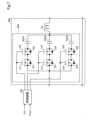
図1は、受電装置である小型モビリティ200向けの送電装置100を示す説明図である。送電装置100は、交流電源10と、電力変換ユニット20と、送電コイル81とを備える。本実施形態では、送電コイル81は、4×5のマトリックス状に配置され、コイルユニット83を構成している。電力変換ユニット20と送電コイル81とは、伝送線路70により接続されている。小型モビリティ200は、例えば、工場において、部品等を運搬する運搬装置である。小型モビリティ200は、受電コイル281を有しており、受電コイル281を用いて送電コイル81から非接触で電力を受電し、工場内を移動する。・First embodiment:
FIG. 1 is an explanatory diagram showing a
図2は、小型モビリティ200を示す説明図である。小型モビリティ200は、バッテリ210と、電力変換ユニット220と、受電コイル281と、を備える。受電コイル281は、送電コイル81と電磁的に結合し、送電コイル81から交流電力を受電する。電力変換ユニット220は、受電コイル281が受電した交流電力を、直流に変換する。電力変換ユニット220は、例えば、ブリッジ整流回路と平滑コンデンサ(図示せず)を備えている。バッテリ210は、電力変換ユニット220により直流に変換された電力を蓄電する。バッテリ210に直電された電力は、小型モビリティ200を動作させる電力として用いられる。 FIG. 2 is an explanatory diagram showing the
図3は、送電装置100の等価回路図である。送電装置100は、交流電源10と、電力変換ユニット20と、補償器60と、伝送線路70と、送電ユニット80と、を備える。電力変換ユニット20は、交流電圧を発生し、伝送線路70を介して交流電圧を送電ユニットに供給する装置である。電力変換ユニット20は、力率改善回路30と、インバータ40と、フィルタ50と、を備え、力率改善回路30は、交流電源10から供給される入力電流に発生する高調波電流を抑制し、力率を1に近づける回路である。インバータ40は、直流電圧を、予め定めた周波数、例えば、85kHzの交流に変換する。フィルタ50は、コイル51とコンデンサ52とから構成されるL型フィルタと、コイル53とコンデンサ54とから構成されるL型フィルタとを直列に接続した構成を有する。 FIG. 3 is an equivalent circuit diagram of the
伝送線路70は、1対の導線で形成されている。伝送線路70は、電気抵抗r72と、インダクタンスL71を有する。図3では、電気抵抗r72、インダクタンスL71を抵抗器、コイルの回路図記号を用いて抵抗器72、コイル71として図示している。送電ユニット80は、直列に接続された送電コイル81と、コンデンサ82とを備える。補償器60は、電力変換ユニット20と伝送線路70との間に、直列に接続された誘導性リアクタンス素子であるコイル61と容量性リアクタンス素子であるコンデンサ62とを備える。補償器60については、後述する。 The
図4は、小型モビリティ200の等価回路図である。小型モビリティ200は、受電ユニット280と、電力変換ユニット220と、バッテリ210とを備える。受電ユニット280は、直列に接続された受電コイル281と、コンデンサ282とを備える。 FIG. 4 is an equivalent circuit diagram of the
図5は、ガウス平面で示す伝送線路70と補償器60における各構成要素のリアクタンスを示す説明図である。ガウス平面において、実軸は電気抵抗を示し、虚軸は、リアクタンスを示す。虚軸のプラス方向へのベクトルが誘導性リアクタンスであり、虚軸のマイナス方向へのベクトルが容量性リアクタンスである。また、虚軸のプラス側が誘導性リアクタンス領域であり、マイナス側が容量性リアクタンス領域である。 FIG. 5 is an explanatory diagram showing the reactance of each component in the
補償器60は、伝送線路70のインダクタンスL71に起因する誘導性リアクタンスの影響を抑制する。補償器60は、上述したように、誘導性リアクタンス素子であるコイル61と容量性リアクタンス素子であるコンデンサ62とを備える。先ず、コイル61を備えない場合について考える。コンデンサ62は、その容量性リアクタンス(1/(jωC62))を用いて、伝送線路70のインダクタンスL71に起因する誘導性リアクタンス(jωL71)を相殺する。ωは、各周波数であり、電力変換ユニット20が発生させる交流電圧の周波数をfとすると、ω=2πfである。伝送線路70の形状がわずかに変化するだけで、伝送線路70のインダクタンスL71が変化する。伝送線路70の形状が変化すると、インダクタンスL71が変化し、リアクタンスが変化し、インピーダンスが変化する。そのため、伝送線路70の形状の変化に伴い、コンデンサ62の容量を変化させることで、伝送効率の悪化を抑制する。電力変換ユニット20から送電ユニット80に交流電力を送る場合、途中の伝送線路70での損失をできるだけ小さくすることが求められる。補償器60がなく伝送線路70のみが、電力変換ユニット20から送電ユニット80の間に設けられているとき、伝送線路70のコイル71とコンデンサ62は、伝送線路70の誘導性リアクタンスを低減し、次式に示される共振条件をできるだけ満たすものとすることが望ましい。具体的には、
jωL71+1/(jωC62)≒0
あるいは、
j(ωL71-1/(ωC62))≒0
を満たすことが望ましい。以下、上記式において、両辺が等しいまたはほぼ等しい場合を含めて、実用上の共振の条件が成立することを、容量性リアクタンス(1/jωC62)により誘導性リアクタンス(jωL71)を相殺するという。
jωL71+1/(jωC62)≒0
or,
j (ωL71-1/(ωC62))≒0
It is desirable to satisfy the following. Hereinafter, in the above equation, it is said that the inductive reactance (jωL71) is canceled by the capacitive reactance (1/jωC62) when the practical resonance conditions are satisfied, including when both sides are equal or almost equal.
本開示では、補償器60は、伝送線路70に直列に接続されたコイル61とコンデンサ62とを備える。コイル61により、伝送線路70のインダクタンスL71と補償器60のコイル61のインダクタンスL61の両方を合わせたインダクタンスを増加させる。この結果、誘導性リアクタンス(jω(L71+L61))が大きくなる。この誘導性リアクタンス(jω(L71+L61))を補償器60のコンデンサ62の容量性リアクタンス(1/(jωC62))を用いて低減し、相殺する。ここで、補償器60のコイル61のインダクタンスL61を伝送線路70のインダクタンスL71よりも十分に大きく、例えば、インダクタンスL61をインダクタンスL71の5倍から10倍程度とすれば、誘導性リアクタンスは、jωL71<<jωL61となる。その結果、伝送線路70と補償器60とを合わせた誘導性リアクタンス(jω(L71+L61))は、ほぼコイル61の誘導性リアクタンス(jωL61)となる。その結果、伝送線路70の形状の変化が発生しても、伝送線路70のインダクタンスL71の影響を無視できる。 In the present disclosure,
この誘導性リアクタンスをちょうど相殺するのに必要なコンデンサ62の容量C62は、1/(ω2L71)である。補償器60にコイル61を設けない場合、伝送線路70のインダクタンスL71に起因する誘導性リアクタンス(jωL71)は小さいので、コンデンサ62の容量C62は、かなり大きな容量となってしまう。一方、補償器60にコイル61を設けた場合、補償器60のコンデンサ62の容量C62は、1/(ω2(L71+L61))でよいので、補償器60のコイル61を設けない場合に比べてコンデンサ62の容量C62を小さくできる。また、L71<<L61であれば、伝送線路70のインダクタンスL71の影響をほぼ無視できるので、補償器60のコイル61のインダクタンスのみを考慮して、コンデンサ62の容量を決めることができる。The capacitance C62 of the
以上説明したように、第1実施形態によれば、補償器60は、直列に接続された、伝送線路70の誘導性リアクタンス(jωL71)よりも大きな誘導性リアクタンス(jωL61)を有する誘導性リアクタンス素子(コイル61)と、コンデンサ62と、を有するので、伝送線路70の誘導性リアクタンスをほぼ無視でき、コイル61の誘導性リアクタンスをコンデンサ62の容量性リアクタンスにより相殺することができる。その結果、伝送線路70の形状が変わること等による誘導性リアクタンスの変化の影響を回避できる。また、コイル61を設けない場合の伝送線路70の誘導性リアクタンス(jωL71)を相殺するのに必要なコンデンサ62の容量は1/(ω2L71)であり、コイル61を設けた場合の伝送線路70と補償器60の誘導性リアクタンス(jω(L71+L61))を相殺するのに必要なコンデンサ62の容量は1/(ω2(L71+L61))であるので、コイル61を設けると、設けない場合に比べて、コンデンサ62の容量を小さくできる。As described above, according to the first embodiment, the
伝送線路70と補償器60の誘導性リアクタンスをコンデンサ62の容量性リアクタンスにより相殺することができる場合、伝送線路70と補償器60とは、共振しているため、電力変換ユニット20から出力される出力電圧Voutの実効値(以下「出力電圧実効値Veout」と呼ぶ。)と、送電ユニット80に入力される入力電圧Vinの実効値(以下「入力電圧実効値Vein」と呼ぶ。)とは、ほぼ等しい。なお、より正確には、入力電圧実効値Veinは、伝送線路70の電気抵抗r72の分だけ出力電圧実効値Veoutから電圧降下する。したがって、Veout-Veinが最小となるように、補償器60のコイル61のインダクタンスと、コンデンサ62の容量を定めることができる。例えば、調整段階において、電力変換ユニット20の出力部と、送電ユニット80の入力部にそれぞれ電圧計を配置して、コンデンサ62の容量を変えながら出力電圧実効値Veoutと入力電圧実効値Veinを測定し、Veout-Veinが最小となるコンデンサ62の容量を求め、その後、電圧計を取り外してもよい。 If the inductive reactance of the
・第2実施形態:
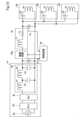
図6は、送電装置100aの等価回路図である。第1実施形態では、補償器60のコイル61のインダクタンスL61と、コンデンサ62の容量C62と、を手動で決定したが、第2実施形態では、制御装置90が、出力電圧実効値Veoutと、入力電圧実効値Veinとを用いて、補償器60aのコンデンサ62aの容量C62aを自動的に設定する点で相違する。・Second embodiment:
FIG. 6 is an equivalent circuit diagram of the
図7は、補償器60aの回路図である。補償器60aは、直列に接続されたコイル61と、コンデンサ62aを備える。コンデンサ62aは、3つのコンデンサ62a1、62a2、62a3と、MOS-FETで形成された半導体スイッチであるスイッチングトランジスタtr1~tr6と、ダイオードD1~D6と、を備える。ダイオードD1~D6は、スイッチングトランジスタtr1~tr6にのドレイン-ソース間に並列に接続されている。このダイオードD1、D3、D5とダイオードD2、D4、D6とは、導通方向が反対向きに接続されている。コンデンサ62a1と、スイッチングトランジスタtr1、tr2は直列に接続されている。コンデンサ62a2と、スイッチングトランジスタtr3、tr4は直列に接続され、コンデンサ62a1と、スイッチングトランジスタtr1、tr2と並列に接続されている。また、コンデンサ62a3と、スイッチングトランジスタtr5、tr6は直列に接続され、コンデンサ62a1と、スイッチングトランジスタtr1、tr2と並列に接続されている。 FIG. 7 is a circuit diagram of the
スイッチングトランジスタtr1、tr2は、同時にオン・オフされる。スイッチングトランジスタtr1、tr2がオンの時には、補償器60には、交流電圧が印加されるので、フィルタ50側が、伝送線路70側よりも高電圧の時には、フィルタ50からスイッチングトランジスタtr1、ダイオードD1、スイッチングトランジスタtr2を経て伝送線路70に電流が流れる。逆に、伝送線路70側が、フィルタ50側よりも高電圧の時には、伝送線路70からスイッチングトランジスタtr2、ダイオードD2、スイッチングトランジスタtr1を経てフィルタ50に電流が流れる。すなわち、コンデンサ62a1に充放電電流が流れる。一方、スイッチングトランジスタtr1、tr2がオフの時には、フィルタ50側が伝送線路70側よりも高電圧の場合には、トランジスタTr2、ダイオードD2に電流が流れず、伝送線路70側がフィルタ50側よりも高電圧の場合には、トランジスタTr1、ダイオードD1に電流が流れないため、フィルタ50と伝送線路70との間に電流が流れない。すなわち、コンデンサ62a1に充放電電流が流れない。スイッチングトランジスタtr3、tr4、ダイオードD3、D4、コンデンサ62a2についても同様であり、スイッチングトランジスタtr5、tr6、ダイオードD5、D5、コンデンサ62a3についても同様である。 Switching transistors tr1 and tr2 are turned on and off simultaneously. When the switching transistors tr1 and tr2 are on, an AC voltage is applied to the
制御装置90は、出力電圧実効値Veoutと、入力電圧実効値Veinとから、スイッチングトランジスタtr1~tr6のどのスイッチングトランジスタをオンし、どのスイッチングトランジスタをオフするかを決定し、コイル61に直列に接続するコンデンサを決定する。なお、制御装置90は、コンデンサ62a1、62a2、62a3の少なくとも1つを接続する。コンデンサ62a1、62a2、62a3の容量C62a1、C62a2、C62a3は、同じ容量であってもよく、異なる容量であってもよい。例えば、容量比をC62a1:C62a2:C62a3=1:2:4としてもよい。この場合、制御装置90が、スイッチングトランジスタtr1、tr2のみをオンにした場合は、コンデンサ62a1のみが接続され、コイル61に接続されるコンデンサ62aの容量が最小となる。また、制御装置90が、スイッチングトランジスタtr1からtr6の全てをオンにした場合は、コンデンサ62a1、62a2、62a3が接続され、コイル61に接続されるコンデンサ62aの容量が最大となる。ガウス平面で、コンデンサ62a1のみが接続された場合のリアクタンスが誘導性領域、すなわち、jωL61>1/(jωC62a1)であり、コンデンサ62a1、62a2、62a3の全てが接続された場合のリアクタンスが容量性領域、すなわち、jωL61<1/(jω(C62a1+C62a2+C62a3))となることが好ましい。コンデンサ62aの容量を増加していくと、リアクタンスが、プラスの値である誘導性領域から、マイナスの値である容量性領域に遷移していき、途中でゼロ点をクロスする。このゼロ点は、共振点であり、出力電圧実効値Veoutと入力電圧実効値Veinの差が最小となる。本実施形態では、コンデンサ62a1、62a2、62a3を切り替える構成としたが、必要な定格電圧を満たす可変容量コンデンサを用いてもよい。 The
図8は、制御装置90が実行するコンデンサ62aの容量決定のフローチャートである。ステップS200では、制御装置90は、コンデンサ62aの容量を最小に設定する。この状態では、コイル61の誘導性リアクタンス(jωL61)の大きさは、コンデンサ62aの容量性リアクタンス(1/(jωC62a))の大きさよりも大きい。 FIG. 8 is a flowchart of determining the capacitance of the
ステップS210では、制御装置90は、電力変換ユニット20の出力電圧Voutと、送電ユニット80に入力される入力電圧Vinと、を取得する。ステップS210では、制御装置90は、出力電圧Voutから出力電圧実効値Veoutを取得し、入力電圧Vintから入力電圧実効値Veinを取得する。ステップS230では、制御装置90は、出力電圧実効値Veoutと入力電圧実効値Veinの電圧差ΔVが判定値ΔVth以下か否かを判断する。判定値ΔVthは、例えば、伝送線路70の電気抵抗r72による電圧降下を考慮して定められる。電圧差ΔVが判定値ΔVth以下の場合には、現在のコンデンサ62aの容量性リアクタンスで、コイル61の誘導性リアクタンスっjωL61を十分に相殺できているので、処理を終了する。電圧差ΔVが判定値ΔVthを超える場合には、処理をステップS240に移行する。 In step S210, the
ステップS240では、制御装置90は、今回測定したときの電圧差Δが前回測定したときの電圧差ΔVよりも増加しているか否かを判断する。制御装置90は、電圧差ΔVが、増加していない場合には、処理をステップS250に移行し、増加している場合には、処理をステップS260に移行する。なお、初めてこのステップS240を処理する場合には、前回測定したときの電圧差ΔVが存在しないため、制御装置90は、ステップS250に移行する。 In step S240, the
ステップS250では、制御装置90は、スイッチングトランジスタtr1からtr6のオン・オフを切り替えて、コンデンサ62aの容量を1段階増加し、その後、処理をステップS210に移行する。ステップS260では、制御装置90は、スイッチングトランジスタtr1からtr6のオン・オフを切り替えて、コンデンサ62aの容量を1段階減少し、処理を終了する。電圧差ΔVが増加している場合は、コンデンサ62aの容量性リアクタンス(1/(jωC62a))がコイル61の誘導性リアクタンスよりも大きくなりすぎたため、容量性リアクタンスによって、インピーダンスが増加し、入力電圧実効値Veinが低下したと考えられるからである。この場合、前回のコンデンサ62aの容量の時に出力電圧実効値Veoutと入力電圧実効値Veinの電圧差ΔVを最も小さくできるからである。 In step S250, the
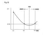
図9は、コンデンサ62aの容量と電圧差ΔVの関係を示す説明図である。制御装置90は、スイッチングトランジスタtr1~tr6を切り替え、コンデンサ62aの容量をC1から、C2、C3と一段階ずつ上昇させていく。コンデンサ62aの容量が増加していくと、電圧差ΔVが下がっていく。コンデンサ62aの容量がC4となったとき、電圧差ΔV(C4)は、判定値ΔVth以下となる。制御装置90は、コンデンサ62aの容量として、C4を採用する。なお、図9に示す例では、コンデンサ62aの容量をC4よりも大きくすると、電位差ΔVは、極小値を経て増加していく。この電位差ΔVの増加は、コンデンサ62aの容量性リアクタンスによるものである。また、本実施形態では、測定値において、電圧差ΔVが最初に判定値ΔVth以下となる点が、電位差ΔVが極小値となる点よりも、誘導性領域にあるが、測定値において、電圧差ΔVが最初に判定値ΔVth以下となる点が、電位差ΔVが極小値となる点よりも容量性領域にあってもよい。 FIG. 9 is an explanatory diagram showing the relationship between the capacitance of the
図10は、コンデンサ62aの容量と電圧差ΔVの関係を示す説明図である。図9との違いは、測定値において、電圧差ΔVが判定値ΔVth以下となる点が存在しない点である。すなわち、図10は、図8のステップS240の判定が「No」であり、ステップS250の判定が「Yes」の場合を示す。図10に示す例では、コンデンサ62aの容量をC2とした場合の電位差ΔV(C2)は、判定値ΔVthよりも大きく、コンデンサ62aの容量をC3とした場合の電位差ΔV(C3)も判定値ΔVthよりも大きい。また、電位差ΔV(C3)は、電位差ΔV(C2)よりも大きい。この場合、制御装置90は、コンデンサ62aの容量として、C2を採用する。この現象は、図10に示すように、コンデンサ62aの容量をC2とした場合のリアクタンスが誘導性領域にあり、コンデンサ62aの容量をC3とした場合のリアクタンスが容量性領域にある場合に発生し得る。また、図には示さないが、コンデンサ62aの容量をC2、C3とした場合のリアクタンスがいずれも容量性領域にある場合にも、発生し得る。 FIG. 10 is an explanatory diagram showing the relationship between the capacitance of the
以上、第2実施形態によれば、補償器60aは、コンデンサ62aとして、3個のコンデンサ62a1、62a2、62a3を含み、制御装置90は、出力電圧実効値Veoutと入力電圧実効値Veinの差により、スイッチングトランジスタtr1からtr6を用いて、3個のコンデンサ62a1、62a2、62a3のうちの少なくとも1つ以上をコンデンサ62aとして接続するように切り替える。その結果、制御装置90は、出力電圧実効値Veoutと入力電圧実効値Veinを取得し、伝送線路70の誘導性リアクタンスの影響を最小にするように、制御できる。その結果、コイル61の誘導性リアクタンスをコンデンサ62aの容量性リアクタンスにより相殺することができ、伝送線路70の形状が変わること等による誘導性リアクタンスの変化の影響を回避できる。 As described above, according to the second embodiment, the
本実施形態では、スイッチとして、MOS-FETであるスイッチングトランジスタを用いたが、他の半導体、例えば、トライアックや、リレーなどの接点型のスイッチを用いてもよい。 In this embodiment, a switching transistor, which is a MOS-FET, is used as the switch, but other semiconductors, such as a triac or a contact type switch such as a relay, may also be used.
本実施形態では、3個のコンデンサ62a1、62a2、62a3を用いたが、m個(mは2以上の自然数)のコンデンサであってもよい。また、コイル61をn個(nは2以上の自然数)設け、接続されるコイル61の数の数を調整してもよい。両者をまとめると、補償器60aは、n個の誘導性リアクタンス素子であるコイルと、m個のコンデンサ(n、mは自然数であり、少なくとも一方は2以上)と、n個のコイルと、m個のコンデンサの組み合わせを変更するスイッチと、を備え、制御装置90は、出力電圧実効値Veoutと、入力電圧実効値Veinとを用いて、スイッチの切り替えを制御し、n個のコイルとm個のコンデンサの組み合わせを制御しても良い。このとき、n個のコイルとm個のコンデンサの全ての組み合わせで出力電圧実効値Veoutと、入力電圧実効値Veinとを取得し、出力電圧実効値Veoutと、入力電圧実効値Veinとの差が最も小さいコイルとコンデンサの組み合わせを採用してもよい。 In this embodiment, three capacitors 62a1, 62a2, and 62a3 are used, but m capacitors (m is a natural number of 2 or more) may be used. Alternatively, n coils 61 (n is a natural number of 2 or more) may be provided, and the number of
・第3実施形態:
図11は、第3実施形態における補償器60bの回路図である。第2実施形態では、補償器60aは、誘導性リアクタンス素子として、コイル61を用いたが、第3実施形態では、補償器60bは、誘導性リアクタンス素子として、コモンモードチョークコイル61bを用いる。コモンモードチョークコイル61bは、電力変換ユニット20の高周波ノイズを除去するためのノイズフィルタとして用いられる。コモンモードチョークコイル61bは、鉄心に巻かれた2つのコイルを有するため、インダクタンスを有しており、コモンモードチョークコイル61bを誘導性リアクタンス素子として機能させることができる。補償器60bのコンデンサ62bの構成は、第2実施形態の補償器60aのコンデンサ62aの構成と同じである。・Third embodiment:
FIG. 11 is a circuit diagram of a compensator 60b in the third embodiment. In the second embodiment, the
以上、第3実施形態においても、補償器60bは、コンデンサ62bとして、3個のコンデンサ62b1、62b2、62b3を含み、制御装置90は、出力電圧実効値Veoutと入力電圧実効値Veinの差により、スイッチングトランジスタtr1からtr6を用いて、3個のコンデンサ62b1、62b2、62b3のうちの少なくとも1つ以上をコンデンサ62bとして接続するように切り替える。その結果、制御装置90は、第2実施形態と同様に、出力電圧実効値Veoutと入力電圧実効値Veinを取得し、伝送線路70の誘導性リアクタンスの影響を最小にするように、制御できる。その結果、コイル61の誘導性リアクタンスをコンデンサ62bの容量性リアクタンスにより相殺することができ、伝送線路70の形状が変わること等による誘導性リアクタンスの変化の影響を回避できる。 As described above, in the third embodiment as well, the
・第4実施形態:
図12は、第4実施形態における補償器60cの回路図である。第2実施形態では、補償器60aは、誘導性リアクタンス素子として、コイル61を用いたが、第4実施形態では、補償器60bは、誘導性リアクタンス素子として、トランス61cを用いる。トランス61cは、鉄心に2つのコイルが巻かれた構造を有するため、インダクタンスを有しており、トランス61cを誘導性リアクタンス素子として機能させることができる。補償器60cのコンデンサ62cの構成は、第2実施形態の補償器60aのコンデンサ62aの構成と同じである。・Fourth embodiment:
FIG. 12 is a circuit diagram of a compensator 60c in the fourth embodiment. In the second embodiment, the
以上、第4実施形態においても、補償器60cは、コンデンサ62bとして、3個のコンデンサ62c1、62c2、62c3を含み、制御装置90は、出力電圧実効値Veoutと入力電圧実効値Veinの差により、スイッチングトランジスタtr1からtr6を用いて、3個のコンデンサ62c1、62c2、62c3のうちの少なくとも1つ以上をコンデンサ62bとして接続するように切り替える。その結果、制御装置90は、第2実施形態と同様に、出力電圧実効値Veoutと入力電圧実効値Veinを取得し、伝送線路70の誘導性リアクタンスの影響を最小にするように、制御できる。その結果、コイル61の誘導性リアクタンスをコンデンサ62cの容量性リアクタンスにより相殺することができ、伝送線路70の形状が変わること等による誘導性リアクタンスの変化の影響を回避できる。 As described above, in the fourth embodiment as well, the
・第5実施形態:
図13は、第5実施形態における送電装置の等価回路図である。第2実施形態では、制御装置90は、出力電圧実効値Veoutと入力電圧実効値Veinとの差によりの差により、スイッチングトランジスタtr1からtr6を用いて、3個のコンデンサ62a1、62a2、62a3のうちの少なくとも1つ以上をコンデンサ62aとして接続するように切り替えた。第5実施形態では、制御装置91は、電力変換ユニット20から出力される出力電圧Voutの位相と、電力変換ユニット20から出力される出力電流Ioutの位相との差によりの差により、スイッチングトランジスタtr1からtr6を用いて、3個のコンデンサ62a1、62a2、62a3のうちの少なくとも1つ以上をコンデンサ62aとして接続するように切り替える点で相違する。・Fifth embodiment:
FIG. 13 is an equivalent circuit diagram of the power transmission device in the fifth embodiment. In the second embodiment, the
図14は、出力電圧と、コンデンサ62aの容量を変えたときの出力電流Ioutを示すグラフである。補償器60aに、コイル61を接続し、コンデンサ62の容量をC1としたときの出力電流Iout(C1)の位相は、出力電圧Voutの位相よりも遅れている。例えば、出力電圧Voutが極大となる位相θVは、出力電流Iout(C1)が極大となる位相θI(C1)よりも遅れている。コンデンサ62の容量をC1からC2に増加すると、出力電流Iout(C2)が極大となる位相θI(C2)は進み、出力電圧Voutが極大となる位相θVに近づく。さらに、コンデンサ62の容量をC3に増加すると、出力電流Iout(C3)が極大となる位相θI(C3)は、出力電圧Voutが極大となる位相θVよりも進む。なお、コンデンサ62の容量をC3よりも増加すると、出力電流Ioutが極大となる位相は、出力電流Iout(C3)が極大となる位相θI(C3)よりも進む。ここで、出力電圧Voutが極大となる位相θVと出力電流圧Iout(C3)が極大となる位相θI(C3)との位相差は、出力電圧Voutが極大となる位相θVと出力電流Iout(C2)が極大となる位相θI(C2)との位相差よりも小さい。したがって、出力電圧Voutが極大となる位相θVと出力電流Iout(C3)が極大となる位相θI(C3)との位相差は、最小となる。したがって、制御装置91は、コンデンサ62aの容量として、C3を採用する。 FIG. 14 is a graph showing the output voltage and the output current Iout when the capacitance of the
以上、第5実施形態によれば、補償器60aは、コンデンサ62aとして、3個のコンデンサ62a1、62a2、62a3を含み、制御装置91は、電力変換ユニット20から出力される出力電圧Voutの位相と、電力変換ユニット20から出力される出力電流Ioutの位相との差によりの差により、スイッチングトランジスタtr1からtr6を用いて、3個のコンデンサ62a1、62a2、62a3のうちの少なくとも1つ以上をコンデンサ62aとして接続するように切り替える。その結果、制御装置91は、伝送線路70の誘導性リアクタンスの影響を最小にするように、制御できる。その結果、コイル61の誘導性リアクタンスをコンデンサ62aの容量性リアクタンスにより相殺することができ、伝送線路70の形状が変わること等による誘導性リアクタンスの変化の影響を回避できる。 As described above, according to the fifth embodiment, the
・第6実施形態:
図15は、第6実施形態における送電装置の等価回路図である。第6実施形態は、1つの伝送線路70に複数の送電ユニット80が接続されている点で、第1~第5実施形態と相違する。しかし、伝送線路70の構成については、第6実施形態は、第1~第5実施形態と同様の構成である。したがって、第1~第5実施形態と同様に、補償器60は、直列に接続された、伝送線路70の誘導性リアクタンス(jωL71)よりも大きな誘導性リアクタンス(jωL61)を有する誘導性リアクタンス素子(コイル61)と、コンデンサ62と、を有するので、伝送線路70の誘導性リアクタンスをほぼ無視でき、コイル61の誘導性リアクタンスをコンデンサ62の容量性リアクタンスにより相殺することができる。その結果、伝送線路70の形状が変わること等による誘導性リアクタンスの変化の影響を回避できる。また、コイル61を設けない場合の伝送線路70の誘導性リアクタンス(jωL71)を相殺するのに必要なコンデンサ62の容量は1/(ω2L71)であり、コイル61を設けた場合の伝送線路70と補償器60の誘導性リアクタンス(jω(L71+L61)を相殺するのに必要なコンデンサ62の容量は1/(ω2(L71+L61))であるので、コイル61を設けると、設けない場合に比べて、コンデンサ62の容量を小さくできる。・Sixth embodiment:
FIG. 15 is an equivalent circuit diagram of the power transmission device in the sixth embodiment. The sixth embodiment differs from the first to fifth embodiments in that a plurality of
上記第1から第4実施形態、第6実施形態では、電力変換ユニット20からの出力電圧Voutの出力電圧実効値Veout、送電ユニット80の入力電圧Vinの入力電圧実効値Veinを用いたが、電力変換ユニット20からの出力電圧Voutのピーク値と、送電ユニット80の入力電圧Vinのピーク値をもちいてもよい。 In the first to fourth embodiments and the sixth embodiment, the output voltage effective value Veout of the output voltage Vout from the
上記第3から第6実施形態において、制御装置90、91がスイッチング素子を切り替えることで、適切なコンデンサの容量を自動的に設定しているが、第1実施形態と同様に、手動で設定してもよい。 In the third to sixth embodiments described above, the
上記各実施形態において、第2実施形態と第5実施形態の組み合わせ、第3実施形態と第4実施形態の組み合わせを含まなければ、任意の実施形態を組み合わせて実施してもよい。 In each of the embodiments described above, any combination of embodiments may be implemented as long as the combination of the second embodiment and the fifth embodiment and the combination of the third embodiment and the fourth embodiment are not included.
第1実施形態から第6実施形態において、送電ユニット80の送電コイル81とコンデンサ82は、直列接続されているとしたが、並列接続されていてもよい。また、第1実施形態から第6実施形態において、補償回路60のコイル61とコンデンサ62は、直列接続されているとしたが、並列接続されていてもよい。また、複数のコイル、コンデンサで構成してもよい。同様に、伝送線路の誘導性リアクタンスをほぼ無視できるようにできる。 In the first to sixth embodiments, the
なお、本開示は、種々の形態で実現することが可能であり、例えば、送電装置の他、送電装置の調整方法、非接触給電システム等の形態で実現することができる。 Note that the present disclosure can be realized in various forms, and for example, in addition to a power transmission device, it can be realized in the form of an adjustment method for a power transmission device, a contactless power supply system, and the like.
本開示は、上述の実施形態に限られるものではなく、その趣旨を逸脱しない範囲において種々の構成で実現することができる。例えば、発明の概要の欄に記載した各形態中の技術的特徴に対応する実施形態の技術的特徴は、上述の課題の一部又は全部を解決するために、あるいは、上述の効果の一部又は全部を達成するために、適宜、差し替えや、組み合わせを行うことが可能である。また、その技術的特徴が本明細書中に必須なものとして説明されていなければ、適宜、削除することが可能である。 The present disclosure is not limited to the embodiments described above, and can be implemented in various configurations without departing from the spirit thereof. For example, the technical features of the embodiments corresponding to the technical features in each form described in the column of the summary of the invention may be Alternatively, in order to achieve all of the above, it is possible to perform appropriate replacements or combinations. Further, unless the technical feature is described as essential in this specification, it can be deleted as appropriate.
10…交流電源、20…電力変換ユニット、30…力率改善回路、40…インバータ、50…フィルタ、51、53…コイル、52、54…コンデンサ、60、60a、60b、60c…補償器、61…コイル、61b…コモンモードチョークコイル、61c…トランス、62、62a、62a1~62a3、62b、62b1~62b3、62c、62c1~62c3…コンデンサ、70…伝送線路、71…コイル、72…抵抗器、80…送電ユニット、81…送電コイル、82…コンデンサ、83…コイルユニット、90、91…制御装置、100、100a…送電装置、200…小型モビリティ、210…バッテリ、220…電力変換ユニット、280…受電ユニット、281…受電コイル、282…コンデンサ、D1~D6…ダイオード、tr1~tr6…スイッチングトランジスタDESCRIPTION OF
Claims (16)
Translated fromJapanese予め定めた周波数の交流電圧を出力する電力変換ユニット(20)と、
送電コイル(81)、および、前記送電コイルに接続されたコンデンサ(82)を有する送電ユニット(80)と、
前記電力変換ユニットと前記送電ユニットとを接続する伝送線路(70)と、
前記電力変換ユニットと前記伝送線路との間に配置される補償器(60)と、
を備え、
前記補償器は、前記伝送線路の誘導性リアクタンスよりも大きな誘導性リアクタンスを有する誘導性リアクタンス素子(61)と、前記伝送線路の誘導性リアクタンスと前記誘導性リアクタンス素子の誘導性リアクタンスとを合わせた誘導性リアクタンスを低減するコンデンサ(62)とを、接続している、送電装置。A power transmission device (100) that supplies power to a power receiving device (200) in a contactless manner,
a power conversion unit (20) that outputs an AC voltage of a predetermined frequency;
a power transmission unit (80) having a power transmission coil (81) and a capacitor (82) connected to the power transmission coil;
a transmission line (70) connecting the power conversion unit and the power transmission unit;
a compensator (60) disposed between the power conversion unit and the transmission line;
Equipped with
The compensator includes an inductive reactance element (61) having an inductive reactance larger than the inductive reactance of the transmission line, and a combination of the inductive reactance of the transmission line and the inductive reactance of the inductive reactance element. A power transmission device connected to a capacitor (62) that reduces inductive reactance.
前記コンデンサの容量は、前記伝送線路の誘導性リアクタンスと前記誘導性リアクタンス素子の誘導性リアクタンスとを合わせた誘導性リアクタンスを相殺できる容量性リアクタンスを生じさせる容量である、送電装置。The power transmission device according to claim 1,
The capacitor has a capacitance that generates a capacitive reactance that can cancel out an inductive reactance that is a combination of an inductive reactance of the transmission line and an inductive reactance of the inductive reactance element.
前記電力変換ユニットの出力電圧(Vout)と、前記送電ユニットの入力電圧(Vin)に応じて、前記誘導性リアクタンス素子のインダクタンスと前記コンデンサの容量が決められている、送電装置。The power transmission device according to claim 1 or 2,
A power transmission device, wherein the inductance of the inductive reactance element and the capacitance of the capacitor are determined according to an output voltage (Vout) of the power conversion unit and an input voltage (Vin) of the power transmission unit.
前記誘導性リアクタンス素子のインダクタンスと前記コンデンサの容量は、前記出力電圧と前記入力電圧との差が判定値(ΔVth)以下となるインダクタンス及び容量である、送電装置。The power transmission device according to claim 3,
In the power transmission device, the inductance of the inductive reactance element and the capacitance of the capacitor are such that a difference between the output voltage and the input voltage is equal to or less than a determination value(ΔVth) .
前記補償器は、n個(nは自然数)の前記誘導性リアクタンス素子と、m個(mは自然数であり、n、mの少なくとも一方は2以上)の前記コンデンサ(62a1~62a3)と、n個の前記誘導性リアクタンス素子とm個の前記コンデンサの組み合わせを変更するスイッチ(tr1~tr6)と、
を備える、送電装置。The power transmission device accordingto claim 3 ,
The compensator includes n inductive reactance elements (n is a natural number), m capacitors (62a1 to 62a3) (m is a natural number, and at least one of n and m is 2 or more), and n switches (tr1 to tr6) for changing the combination of the inductive reactance elements and the m capacitors;
A power transmission device comprising:
前記出力電圧と、前記入力電圧との電圧差が、判定値(ΔVth)以下となるように、前記スイッチによるn個の前記誘導性リアクタンス素子と、m個の前記コンデンサの組み合わせの切り替えを制御する制御装置を備える、送電装置。The power transmission device according to claim 5, further comprising:
Controlling switching of the combination of the n inductive reactance elements and the m capacitors by the switch so that the voltage difference between the output voltage and the input voltage is equal to or less than a determination value (ΔVth). A power transmission device including a control device.
前記電力変換ユニットの出力電圧(Vout)と、前記電力変換ユニットから出力される出力電流(Iout)に応じて、前記誘導性リアクタンス素子のインダクタンスと前記コンデンサの容量が決められている、送電装置。The power transmission device according to claim 1 or 2,
A power transmission device, wherein the inductance of the inductive reactance element and the capacitance of the capacitor are determined according to an output voltage (Vout) of the power conversion unit and an output current (Iout) output from the power conversion unit.
前記誘導性リアクタンス素子のインダクタンスと前記コンデンサの容量は、前記出力電圧の位相と、前記出力電流の位相との差が最小となるインダクタンス及び容量である、送電装置。The power transmission device according to claim 7,
In the power transmission device, the inductance of the inductive reactance element and the capacitance of the capacitor are such that a difference between a phase of the output voltage and a phase of the output current isminimized .
前記補償器は、n個(nは自然数)の前記誘導性リアクタンス素子と、m個(mは自然数であり、n、mの少なくとも一方は2以上)の前記コンデンサと、前記誘導性リアクタンス素子と前記コンデンサの組み合わせを変更するスイッチと、
を備える、送電装置。The power transmission device according to claim 7 or claim 8,
The compensator includes n inductive reactance elements (n is a natural number), m capacitors (m is a natural number, and at least one of n and m is 2 or more), and the inductive reactance elements. a switch for changing the combination of the capacitors;
A power transmission device comprising:
前記出力電圧の位相と、前記出力電流の位相との差が最小となるように、前記スイッチによるn個の前記誘導性リアクタンス素子と、m個の前記コンデンサの組み合わせの切り替えを制御する制御装置を備える、送電装置。The power transmission device according to claim 9, further comprising:
A control device that controls switching of the combinations of the n inductive reactance elements and the m capacitors by the switch so that the difference between the phase of the output voltage and the phase of the output current isminimized . Equipped with a power transmission device.
前記スイッチは、半導体スイッチである、送電装置。The power transmission device according to any one of claims 5, 6, 9, and 10,
The power transmission device, wherein the switch is a semiconductor switch.
前記誘導性リアクタンス素子は、コイル(61)またはトランス(61c)である、送電装置。The power transmission device according to any one of claims 1 to 11,
A power transmission device in which the inductive reactance element is a coil (61) or a transformer (61c).
前記電力変換ユニットは、コイルを含むノイズフィルタ(61b)を有し、
前記誘導性リアクタンス素子として前記ノイズフィルタのコイルを用いる、送電装置。The power transmission device according to claim 1 or claim 11,
The power conversion unit has a noise filter (61b) including a coil,
A power transmission device using a coil of the noise filter as the inductive reactance element.
1つの前記電力変換ユニットに2以上の前記送電ユニットが接続されている、送電装置。The power transmission device according to any one of claims 1 to 13,
A power transmission device in which two or more of the power transmission units are connected to one power conversion unit.
前記電力変換ユニットと前記伝送線路との間に、前記伝送線路の誘導性リアクタンスよりも大きな誘導性リアクタンスを有する誘導性リアクタンス素子と、コンデンサを配置し、
前記電力変換ユニットの出力電圧と、前記送電ユニットの入力電圧とを測定し、
前記出力電圧と前記入力電圧との差が判定値(ΔVth)以下となるように、前記誘導性リアクタンス素子のインダクタンスと前記コンデンサの容量とを調整する、送電装置の調整方法。A method for adjusting a power transmission device that supplies power from a power conversion unit that outputs an AC voltage to a power transmission unit having a power transmission coil and a capacitor connected to the power transmission coil via a transmission line, the method comprising:
disposing an inductive reactance element having an inductive reactance larger than an inductive reactance of the transmission line and a capacitor between the power conversion unit and the transmission line,
measuring the output voltage of the power conversion unit and the input voltage of the power transmission unit;
A method for adjusting a power transmission device, comprising adjusting an inductance of the inductive reactance element and a capacitance of the capacitorso that a difference between the output voltage and the input voltage is equal to or less than a determination value (ΔVth) .
前記電力変換ユニットと前記伝送線路との間に、前記伝送線路の誘導性リアクタンスよりも大きな誘導性リアクタンスを有する誘導性リアクタンス素子と、コンデンサを配置し、
前記電力変換ユニットから出力される出力電圧と、前記電力変換ユニットから出力される出力電流とを測定し、
前記出力電圧の位相と前記出力電流の位相との差が最小となるように、前記誘導性リアクタンス素子のインダクタンスと前記コンデンサの容量とを調整する、送電装置の調整方法。A method for adjusting a power transmission device that supplies power from a power conversion unit that outputs an AC voltage to a power transmission unit having a power transmission coil and a capacitor connected to the power transmission coil via a transmission line, the method comprising:
disposing an inductive reactance element having an inductive reactance larger than an inductive reactance of the transmission line and a capacitor between the power conversion unit and the transmission line,
Measuring the output voltage output from the power conversion unit and the output current output from the power conversion unit,
A method for adjusting a power transmission device, comprising adjusting aninductance of the inductive reactance element and a capacitance of the capacitorso that a difference between a phase of the output voltage and a phase of the output current is minimized .
Priority Applications (5)
| Application Number | Priority Date | Filing Date | Title |
|---|---|---|---|
| JP2021053141AJP7409344B2 (en) | 2021-03-26 | 2021-03-26 | Contactless power transmission device and its adjustment method |
| PCT/JP2022/007598WO2022202075A1 (en) | 2021-03-26 | 2022-02-24 | Non-contact power transmission device and method for adjusting same |
| CN202280024362.7ACN117063373A (en) | 2021-03-26 | 2022-02-24 | Non-contact power transmission device and adjustment method thereof |
| EP22774873.8AEP4316895A4 (en) | 2021-03-26 | 2022-02-24 | NON-CONTACT POWER TRANSMISSION DEVICE AND ITS ADJUSTMENT METHOD |
| US18/369,490US12355262B2 (en) | 2021-03-26 | 2023-09-18 | Contactless power transmission apparatus and adjustment method thereof |
Applications Claiming Priority (1)
| Application Number | Priority Date | Filing Date | Title |
|---|---|---|---|
| JP2021053141AJP7409344B2 (en) | 2021-03-26 | 2021-03-26 | Contactless power transmission device and its adjustment method |
Publications (2)
| Publication Number | Publication Date |
|---|---|
| JP2022150509A JP2022150509A (en) | 2022-10-07 |
| JP7409344B2true JP7409344B2 (en) | 2024-01-09 |
Family
ID=83397051
Family Applications (1)
| Application Number | Title | Priority Date | Filing Date |
|---|---|---|---|
| JP2021053141AActiveJP7409344B2 (en) | 2021-03-26 | 2021-03-26 | Contactless power transmission device and its adjustment method |
Country Status (5)
| Country | Link |
|---|---|
| US (1) | US12355262B2 (en) |
| EP (1) | EP4316895A4 (en) |
| JP (1) | JP7409344B2 (en) |
| CN (1) | CN117063373A (en) |
| WO (1) | WO2022202075A1 (en) |
Citations (4)
| Publication number | Priority date | Publication date | Assignee | Title |
|---|---|---|---|---|
| JP2012010546A (en) | 2010-06-28 | 2012-01-12 | Equos Research Co Ltd | Non-contact power transmission system, non-contact power transmission device, and impedance adjustment method |
| JP2016192856A (en) | 2015-03-31 | 2016-11-10 | 株式会社ダイヘン | Contactless power supply system and power transmission apparatus |
| JP2018007462A (en) | 2016-07-05 | 2018-01-11 | 株式会社ダイヘン | Non-contact power transmission system |
| JP2019017167A (en) | 2017-07-05 | 2019-01-31 | 株式会社ダイヘン | Power transmission system and non-contact power supply system |
Family Cites Families (13)
| Publication number | Priority date | Publication date | Assignee | Title |
|---|---|---|---|---|
| US8884468B2 (en)* | 2007-12-21 | 2014-11-11 | Access Business Group International Llc | Circuitry for inductive power transfer |
| US8855554B2 (en)* | 2008-03-05 | 2014-10-07 | Qualcomm Incorporated | Packaging and details of a wireless power device |
| JP2009268181A (en)* | 2008-04-22 | 2009-11-12 | Olympus Corp | Energy supply apparatus |
| US9963040B2 (en)* | 2012-09-13 | 2018-05-08 | Toyota Jidosha Kabushiki Kaisha | Non-contact power supply system, and power transmission device and vehicle used therein |
| TWI565176B (en)* | 2012-09-28 | 2017-01-01 | Wow Tech Corp | Non-select induction transmission equipment |
| WO2017136491A1 (en)* | 2016-02-02 | 2017-08-10 | Witricity Corporation | Controlling wireless power transfer systems |
| US10491027B2 (en)* | 2016-04-01 | 2019-11-26 | Intel Corporation | Wireless power transmission |
| WO2017218856A1 (en)* | 2016-06-15 | 2017-12-21 | The Regents Of The University Of Colorado, A Body Corporate | Active variable reactance rectifier circuit and related techniques |
| US12348050B2 (en)* | 2017-07-26 | 2025-07-01 | The Regents Of The University Of Colorado, A Body Corporate | Variable compensation inverter circuit and related techniques |
| CN113169587B (en)* | 2018-11-30 | 2022-04-15 | 韦特里西提公司 | System and method for low power excitation in high power wireless power systems |
| CN110048520A (en)* | 2019-05-08 | 2019-07-23 | 燕山大学 | Primary side has the wireless charging device of C-LCC compensation network |
| US11916404B1 (en)* | 2021-05-12 | 2024-02-27 | Ut-Battelle, Llc | Tuning circuitry for a wireless power system |
| JP7487720B2 (en)* | 2021-11-05 | 2024-05-21 | 株式会社ダイフク | NON-CONTACT POWER SUPPLY EQUIPMENT, METHOD FOR ADJUSTING IMPEDANCE OF NON-CONTACT POWER SUPPLY EQUIPMENT, AND IMPEDANCE ADJUSTMENT PROGRAM FOR NON-CONTACT POWER SUPPLY EQUIPMENT |
- 2021
- 2021-03-26JPJP2021053141Apatent/JP7409344B2/enactiveActive
- 2022
- 2022-02-24EPEP22774873.8Apatent/EP4316895A4/enactivePending
- 2022-02-24CNCN202280024362.7Apatent/CN117063373A/enactivePending
- 2022-02-24WOPCT/JP2022/007598patent/WO2022202075A1/ennot_activeCeased
- 2023
- 2023-09-18USUS18/369,490patent/US12355262B2/enactiveActive
Patent Citations (4)
| Publication number | Priority date | Publication date | Assignee | Title |
|---|---|---|---|---|
| JP2012010546A (en) | 2010-06-28 | 2012-01-12 | Equos Research Co Ltd | Non-contact power transmission system, non-contact power transmission device, and impedance adjustment method |
| JP2016192856A (en) | 2015-03-31 | 2016-11-10 | 株式会社ダイヘン | Contactless power supply system and power transmission apparatus |
| JP2018007462A (en) | 2016-07-05 | 2018-01-11 | 株式会社ダイヘン | Non-contact power transmission system |
| JP2019017167A (en) | 2017-07-05 | 2019-01-31 | 株式会社ダイヘン | Power transmission system and non-contact power supply system |
Also Published As
| Publication number | Publication date |
|---|---|
| US20240006923A1 (en) | 2024-01-04 |
| JP2022150509A (en) | 2022-10-07 |
| US12355262B2 (en) | 2025-07-08 |
| EP4316895A1 (en) | 2024-02-07 |
| EP4316895A4 (en) | 2024-12-11 |
| CN117063373A (en) | 2023-11-14 |
| WO2022202075A1 (en) | 2022-09-29 |
Similar Documents
| Publication | Publication Date | Title |
|---|---|---|
| JP7161548B2 (en) | DCDC converters, onboard chargers and electric vehicles | |
| JP4198388B2 (en) | Resonant type converter | |
| CN100472926C (en) | Resonant switching power supply device | |
| US7141892B2 (en) | Power supply method of a line interactive UPS and the line interactive UPS | |
| WO2018179576A1 (en) | Llc resonant converter | |
| US20110080056A1 (en) | Method and apparatus for contactless power transfer | |
| CN107820669B (en) | Double-bridge DC/DC power converter | |
| CN104300698A (en) | A resonance-enhanced wireless power transfer structure with high resonance frequency stability | |
| CN113794288B (en) | A wireless power transmission compensation topology with dual parallel inductors | |
| Bui et al. | DC-DC converter based impedance matching for maximum power transfer of CPT system with high efficiency | |
| Bagchi et al. | Analysis and design of a wireless charger for underwater vehicles fed from a constant current distribution cable | |
| Yang et al. | A hybrid load matching method for WPT systems to maintain high efficiency over wide load range | |
| JP7409344B2 (en) | Contactless power transmission device and its adjustment method | |
| CN118920721A (en) | Reconfigurable compensation wireless charging system and constant voltage and constant current switching and parameter design and coil offset resistance design method | |
| US20220337092A1 (en) | Inductive power transfer system control | |
| KR102236576B1 (en) | Wireless power transfer system | |
| JP2011176973A (en) | Resonance type switching power supply device | |
| WO2001089754A2 (en) | Arc welding generator with input voltage adapting regulator stage | |
| JP2023079300A (en) | Power conversion device | |
| Wei et al. | A Partial-Power-Processed CLLC-DAB DC/DC Transformer with Voltage Self-Balancing Capability for Bipolar LVDC Distribution Systems | |
| EP3738201A1 (en) | Auxiliary converter circuit and its method of operation | |
| JPH10164861A (en) | Resonance inverter circuit | |
| JP7738800B2 (en) | Power transmission device and wireless power supply system | |
| CN211239699U (en) | Double-switch high-voltage-change inverse-modulation power-change compensation alternating current voltage stabilizer | |
| JP7508991B2 (en) | Capacitively isolated power converter |
Legal Events
| Date | Code | Title | Description |
|---|---|---|---|
| A621 | Written request for application examination | Free format text:JAPANESE INTERMEDIATE CODE: A621 Effective date:20221201 | |
| A131 | Notification of reasons for refusal | Free format text:JAPANESE INTERMEDIATE CODE: A131 Effective date:20230926 | |
| A521 | Request for written amendment filed | Free format text:JAPANESE INTERMEDIATE CODE: A523 Effective date:20231110 | |
| TRDD | Decision of grant or rejection written | ||
| A01 | Written decision to grant a patent or to grant a registration (utility model) | Free format text:JAPANESE INTERMEDIATE CODE: A01 Effective date:20231121 | |
| A61 | First payment of annual fees (during grant procedure) | Free format text:JAPANESE INTERMEDIATE CODE: A61 Effective date:20231204 | |
| R151 | Written notification of patent or utility model registration | Ref document number:7409344 Country of ref document:JP Free format text:JAPANESE INTERMEDIATE CODE: R151 |