JP7407967B2 - Display assembly, display device, and fingerprint recognition method - Google Patents
Display assembly, display device, and fingerprint recognition methodDownload PDFInfo
- Publication number
- JP7407967B2 JP7407967B2JP2022559713AJP2022559713AJP7407967B2JP 7407967 B2JP7407967 B2JP 7407967B2JP 2022559713 AJP2022559713 AJP 2022559713AJP 2022559713 AJP2022559713 AJP 2022559713AJP 7407967 B2JP7407967 B2JP 7407967B2
- Authority
- JP
- Japan
- Prior art keywords
- fingerprint recognition
- fingerprint
- signal line
- gate
- active layer
- Prior art date
- Legal status (The legal status is an assumption and is not a legal conclusion. Google has not performed a legal analysis and makes no representation as to the accuracy of the status listed.)
- Active
Links
Images


Classifications
- H—ELECTRICITY
- H10—SEMICONDUCTOR DEVICES; ELECTRIC SOLID-STATE DEVICES NOT OTHERWISE PROVIDED FOR
- H10K—ORGANIC ELECTRIC SOLID-STATE DEVICES
- H10K59/00—Integrated devices, or assemblies of multiple devices, comprising at least one organic light-emitting element covered by group H10K50/00
- H10K59/40—OLEDs integrated with touch screens
- G—PHYSICS
- G02—OPTICS
- G02F—OPTICAL DEVICES OR ARRANGEMENTS FOR THE CONTROL OF LIGHT BY MODIFICATION OF THE OPTICAL PROPERTIES OF THE MEDIA OF THE ELEMENTS INVOLVED THEREIN; NON-LINEAR OPTICS; FREQUENCY-CHANGING OF LIGHT; OPTICAL LOGIC ELEMENTS; OPTICAL ANALOGUE/DIGITAL CONVERTERS
- G02F1/00—Devices or arrangements for the control of the intensity, colour, phase, polarisation or direction of light arriving from an independent light source, e.g. switching, gating or modulating; Non-linear optics
- G02F1/01—Devices or arrangements for the control of the intensity, colour, phase, polarisation or direction of light arriving from an independent light source, e.g. switching, gating or modulating; Non-linear optics for the control of the intensity, phase, polarisation or colour
- G02F1/13—Devices or arrangements for the control of the intensity, colour, phase, polarisation or direction of light arriving from an independent light source, e.g. switching, gating or modulating; Non-linear optics for the control of the intensity, phase, polarisation or colour based on liquid crystals, e.g. single liquid crystal display cells
- G02F1/133—Constructional arrangements; Operation of liquid crystal cells; Circuit arrangements
- G02F1/1333—Constructional arrangements; Manufacturing methods
- G02F1/13338—Input devices, e.g. touch panels
- G—PHYSICS
- G06—COMPUTING OR CALCULATING; COUNTING
- G06V—IMAGE OR VIDEO RECOGNITION OR UNDERSTANDING
- G06V40/00—Recognition of biometric, human-related or animal-related patterns in image or video data
- G06V40/10—Human or animal bodies, e.g. vehicle occupants or pedestrians; Body parts, e.g. hands
- G06V40/12—Fingerprints or palmprints
- G06V40/13—Sensors therefor
- G06V40/1318—Sensors therefor using electro-optical elements or layers, e.g. electroluminescent sensing
- H—ELECTRICITY
- H10—SEMICONDUCTOR DEVICES; ELECTRIC SOLID-STATE DEVICES NOT OTHERWISE PROVIDED FOR
- H10K—ORGANIC ELECTRIC SOLID-STATE DEVICES
- H10K39/00—Integrated devices, or assemblies of multiple devices, comprising at least one organic radiation-sensitive element covered by group H10K30/00
- H10K39/30—Devices controlled by radiation
- H10K39/32—Organic image sensors
- H10K39/34—Organic image sensors integrated with organic light-emitting diodes [OLED]
- H—ELECTRICITY
- H10—SEMICONDUCTOR DEVICES; ELECTRIC SOLID-STATE DEVICES NOT OTHERWISE PROVIDED FOR
- H10K—ORGANIC ELECTRIC SOLID-STATE DEVICES
- H10K59/00—Integrated devices, or assemblies of multiple devices, comprising at least one organic light-emitting element covered by group H10K50/00
- H10K59/10—OLED displays
- H10K59/12—Active-matrix OLED [AMOLED] displays
- H10K59/123—Connection of the pixel electrodes to the thin film transistors [TFT]
- H—ELECTRICITY
- H10—SEMICONDUCTOR DEVICES; ELECTRIC SOLID-STATE DEVICES NOT OTHERWISE PROVIDED FOR
- H10K—ORGANIC ELECTRIC SOLID-STATE DEVICES
- H10K59/00—Integrated devices, or assemblies of multiple devices, comprising at least one organic light-emitting element covered by group H10K50/00
- H10K59/10—OLED displays
- H10K59/12—Active-matrix OLED [AMOLED] displays
- H10K59/131—Interconnections, e.g. wiring lines or terminals
- H—ELECTRICITY
- H10—SEMICONDUCTOR DEVICES; ELECTRIC SOLID-STATE DEVICES NOT OTHERWISE PROVIDED FOR
- H10K—ORGANIC ELECTRIC SOLID-STATE DEVICES
- H10K59/00—Integrated devices, or assemblies of multiple devices, comprising at least one organic light-emitting element covered by group H10K50/00
- H10K59/60—OLEDs integrated with inorganic light-sensitive elements, e.g. with inorganic solar cells or inorganic photodiodes
- H10K59/65—OLEDs integrated with inorganic image sensors
- H—ELECTRICITY
- H10—SEMICONDUCTOR DEVICES; ELECTRIC SOLID-STATE DEVICES NOT OTHERWISE PROVIDED FOR
- H10K—ORGANIC ELECTRIC SOLID-STATE DEVICES
- H10K59/00—Integrated devices, or assemblies of multiple devices, comprising at least one organic light-emitting element covered by group H10K50/00
- H10K59/10—OLED displays
- H10K59/12—Active-matrix OLED [AMOLED] displays
Landscapes
- Physics & Mathematics (AREA)
- Engineering & Computer Science (AREA)
- Chemical & Material Sciences (AREA)
- Inorganic Chemistry (AREA)
- Nonlinear Science (AREA)
- General Physics & Mathematics (AREA)
- Microelectronics & Electronic Packaging (AREA)
- Life Sciences & Earth Sciences (AREA)
- Sustainable Development (AREA)
- Theoretical Computer Science (AREA)
- Multimedia (AREA)
- Mathematical Physics (AREA)
- Crystallography & Structural Chemistry (AREA)
- Human Computer Interaction (AREA)
- Optics & Photonics (AREA)
- Image Input (AREA)
- Devices For Indicating Variable Information By Combining Individual Elements (AREA)
- Measurement Of The Respiration, Hearing Ability, Form, And Blood Characteristics Of Living Organisms (AREA)
- Electroluminescent Light Sources (AREA)
- Solid State Image Pick-Up Elements (AREA)
Description
Translated fromJapanese本出願は、参照によりその全体が本明細書に組み込まれる、2020年3月31日に中国国家知識産権局に出願され、「DISPLAY ASSEMBLY,DISPLAY APPARATUS,AND FINGERPRINT RECOGNITION METHOD」と題する、中国特許出願第202010246037.8号の優先権を主張する。 This application is filed with the State Intellectual Property Office of China on March 31, 2020, and is filed with the China Patent Office entitled "DISPLAY ASSEMBLY, DISPLAY APPARATUS, AND FINGERPRINT RECOGNITION METHOD," which is hereby incorporated by reference in its entirety. Claims priority of application No. 202010246037.8.
本出願は、ディスプレイ技術の分野に関し、より具体的には、ディスプレイ組立体、ディスプレイ装置、およびフィンガプリント認識方法に関する。 TECHNICAL FIELD This application relates to the field of display technology, and more particularly to display assemblies, display devices, and fingerprint recognition methods.
現在、スクリーン内光学式フィンガプリント認識は、現在の電子装置の識別認識のための主流の方法となってきている。ディスプレイパネルの基板の裏面側に光学式フィンガプリント認識モジュールが配置され、フィンガプリント認識光源が放射する光を指に照射する。指によって反射された後、光はディスプレイパネルを透過し、その後、感光要素で受け取られ、光信号を電気信号に変換する。これによりフィンガプリント認識が実装される。従来技術における解決策では、フィンガプリント認識のために使用される光がディスプレイパネルの厚さ方向にディスプレイパネル全体を透過した後は、光損失が大きい。このことは、感光要素が受け取る光の量に重大な影響を与え、さらにフィンガプリント認識の精度にも影響を与える。 Currently, in-screen optical fingerprint recognition has become the mainstream method for identification recognition of modern electronic devices. An optical fingerprint recognition module is disposed on the back side of the substrate of the display panel, and irradiates the finger with light emitted from a fingerprint recognition light source. After being reflected by the finger, the light is transmitted through the display panel and then received by a photosensitive element, which converts the optical signal into an electrical signal. This implements fingerprint recognition. In prior art solutions, the light loss is high after the light used for fingerprint recognition passes through the entire display panel in the thickness direction of the display panel. This has a significant impact on the amount of light received by the photosensitive element, which in turn impacts the accuracy of fingerprint recognition.
これを考慮して、本出願は、従来技術におけるフィンガプリント認識精度の低さという技術的課題を解決するために、ディスプレイ組立体、ディスプレイ装置、およびフィンガプリント認識方法を提供する。 In view of this, the present application provides a display assembly, a display device, and a fingerprint recognition method to solve the technical problem of low fingerprint recognition accuracy in the prior art.
第1の態様によれば、本出願の実施形態は、ディスプレイパネルと、ディスプレイパネルの発光面上に配置されたフィンガプリント認識モジュールとを含むディスプレイ組立体を提供する。フィンガプリント認識モジュールは、複数のフィンガプリント認識ユニットを含み、各フィンガプリント認識ユニットは、少なくとも1つのフォトトランジスタおよび1つのスイッチトランジスタを含む。 According to a first aspect, embodiments of the present application provide a display assembly including a display panel and a fingerprint recognition module disposed on a light emitting surface of the display panel. The fingerprint recognition module includes a plurality of fingerprint recognition units, each fingerprint recognition unit including at least one phototransistor and one switch transistor.
フォトトランジスタは、第1の活性層、第1のゲート、第1のソース、および第1のドレインを含む。第1の活性層を作製するための材料は、有機半導体材料を含む。ディスプレイ組立体に垂直な方向において、第1のドレインおよび第1のゲートは部分的に重なり合って第1のキャパシタを形成する。 The phototransistor includes a first active layer, a first gate, a first source, and a first drain. The material for making the first active layer includes an organic semiconductor material. In a direction perpendicular to the display assembly, the first drain and the first gate partially overlap to form a first capacitor.
スイッチトランジスタは、第2の活性層、第2のゲート、第2のソース、および第2のドレインを含む。 The switch transistor includes a second active layer, a second gate, a second source, and a second drain.
フィンガプリント認識モジュールは、第1の金属層を含む。第1のソース、第1のドレイン、第2のソース、および第2のドレインは、すべて第1の金属層に位置し、第1のドレインは第2のソースに接続されている。 The fingerprint recognition module includes a first metal layer. A first source, a first drain, a second source, and a second drain are all located in the first metal layer, and the first drain is connected to the second source.
本出願の本実施形態では、フィンガプリント認識モジュールは、ディスプレイパネルの発光面に配置される。フィンガプリント認識の間、指によって反射された光は、ディスプレイパネルの構造フィルム層を透過することなしに、フィンガプリント認識モジュールによって受け取られ得る。これにより、フィンガプリント反射光の透過距離が短くされ得、フィンガプリント反射光のコリメーションが改善され、フィンガプリント反射光がディスプレイパネルの構造フィルム層を透過する際の光損失が回避され、フィンガプリント認識精度が確実にされ得る。さらに、フォトトランジスタは、フィンガプリント認識モジュールにおける感光要素として使用される。フォトトランジスタの構造は、スイッチトランジスタの構造と同様である。作製中、フォトトランジスタおよびスイッチトランジスタは、作製プロセスの少なくとも一部を共有し得る。これにより、ディスプレイ組立体の構造およびプロセスの複雑さを低減し得、また、ディスプレイ組立体の全体の厚さを低減し得る。 In this embodiment of the present application, the fingerprint recognition module is placed on the light emitting surface of the display panel. During fingerprint recognition, the light reflected by the finger can be received by the fingerprint recognition module without passing through the structural film layer of the display panel. This can shorten the transmission distance of the fingerprint reflected light, improve the collimation of the fingerprint reflected light, avoid light loss when the fingerprint reflected light passes through the structural film layer of the display panel, and improve fingerprint recognition. Accuracy can be ensured. Furthermore, phototransistors are used as photosensitive elements in fingerprint recognition modules. The structure of the phototransistor is similar to that of the switch transistor. During fabrication, the phototransistor and switch transistor may share at least a portion of the fabrication process. This may reduce the structural and process complexity of the display assembly and may also reduce the overall thickness of the display assembly.
さらに、フィンガプリント認識モジュールは、第2の金属層および第1の絶縁層をさらに含む。第2の金属層は、第1の金属層の側、かつディスプレイパネルに近い側に位置している。第1の絶縁層は、第1の金属層と第2の金属層との間に位置する。第1のゲートは、第2の金属層に位置する。フォトトランジスタは、ボトムゲート構造のトランジスタであり、第1のゲートは、第1の活性層に放射される光を遮蔽しない。これにより、フィンガプリント認識段階においてフィンガプリント反射光が第1の活性層に照射され得、フォトトランジスタが光信号を電気信号に変換することが確実になる。 Furthermore, the fingerprint recognition module further includes a second metal layer and a first insulating layer. The second metal layer is located on the side of the first metal layer and closer to the display panel. The first insulating layer is located between the first metal layer and the second metal layer. The first gate is located in the second metal layer. The phototransistor is a bottom-gate transistor, and the first gate does not block light emitted to the first active layer. This ensures that the fingerprint reflected light can be irradiated onto the first active layer during the fingerprint recognition step and that the phototransistor converts the optical signal into an electrical signal.
さらに、第1の活性層と第2の活性層との両方は、第1の絶縁層の側、かつ第2の金属層から離れた側に位置し、第1の絶縁層と接している。これは、第1の活性層および第2の活性層が同じフィルム層の高さに位置していることと同等である。これは、フィンガプリント認識モジュールのフィルム層の厚さを減少させるのに役立ち、さらに、ディスプレイ組立体の全体の厚さを減少させるのに役立ち得る。 Furthermore, both the first active layer and the second active layer are located on the side of the first insulating layer and away from the second metal layer, and are in contact with the first insulating layer. This is equivalent to the first active layer and the second active layer being located at the same film layer height. This helps reduce the thickness of the film layer of the fingerprint recognition module, which may further help reduce the overall thickness of the display assembly.
一実施形態では、第1のソースは、第1のゲートに接続されず、フィンガプリント認識モジュールは、フィンガプリント制御信号線、フィンガプリントデータ信号線、第1の電圧信号線、および第2の電圧信号線を含む。第2のゲートはフィンガプリント制御信号線に電気的に接続され、第2のドレインはフィンガプリントデータ信号線に電気的に接続され、第1のゲートは第1の電圧信号線に電気的に接続され、第1のソースは第2の電圧信号線に電気的に接続されている。フィンガプリント認識フェーズにおいて、第1の電圧信号線によって第1のゲートに供給される電圧は、第2の電圧信号線によって第1のソースに供給される電圧よりも大きい。 In one embodiment, the first source is not connected to the first gate, and the fingerprint recognition module is connected to the fingerprint control signal line, the fingerprint data signal line, the first voltage signal line, and the second voltage signal line. Contains signal lines. The second gate is electrically connected to the fingerprint control signal line, the second drain is electrically connected to the fingerprint data signal line, and the first gate is electrically connected to the first voltage signal line. and the first source is electrically connected to the second voltage signal line. During the fingerprint recognition phase, the voltage supplied to the first gate by the first voltage signal line is greater than the voltage supplied to the first source by the second voltage signal line.
一実施形態では、第1のソースは、第1の絶縁層におけるビアを介して第1のゲートに接続されている。フォトトランジスタの第1のゲートおよび第1のソースが接続されているので、フォトトランジスタは常にオフ状態で動作する。この場合、第1の活性層の表面に光が照射されないとき、フォトトランジスタのリーク電流は非常に小さい。しかしながら、フィンガプリント認識段階において、フィンガプリント反射光が第1の活性層の表面に照射されるとき、第1の活性層の内部で生成されるキャリアによって、フォトトランジスタのリーク電流が顕著に増大することができるので、フォトトランジスタの光感度が高くなることが確実にされ得る。 In one embodiment, the first source is connected to the first gate via a via in the first insulating layer. Since the first gate and first source of the phototransistor are connected, the phototransistor always operates in an off state. In this case, when the surface of the first active layer is not irradiated with light, the leakage current of the phototransistor is very small. However, in the fingerprint recognition stage, when the surface of the first active layer is irradiated with the fingerprint reflected light, the leakage current of the phototransistor increases significantly due to carriers generated inside the first active layer. Therefore, it can be ensured that the photosensitivity of the phototransistor is high.
フィンガプリント認識モジュールは、フィンガプリント制御信号線、フィンガプリントデータ信号線、および第3の電圧信号線を含む。 The fingerprint recognition module includes a fingerprint control signal line, a fingerprint data signal line, and a third voltage signal line.
第2のゲートはフィンガプリント制御信号線に電気的に接続され、第2のドレインはフィンガプリントデータ信号線に電気的に接続され、第1のゲートおよび第1のソースの両方は第3の電圧信号線に電気的に接続されている。フィンガプリント認識モジュールに配置する必要があるのは、フィンガプリント制御信号線、フィンガプリントデータ信号線、および第3の電圧信号線の、3タイプの信号線のみである。これにより、フィンガプリント認識モジュールにおける配線方法が簡素化され、配線に占有されるスペースも削減され得る。 The second gate is electrically connected to the fingerprint control signal line, the second drain is electrically connected to the fingerprint data signal line, and both the first gate and the first source are connected to a third voltage. Electrically connected to the signal line. Only three types of signal lines need to be placed in the fingerprint recognition module: a fingerprint control signal line, a fingerprint data signal line, and a third voltage signal line. This simplifies the wiring method in the fingerprint recognition module and can also reduce the space occupied by the wiring.
任意選択で、第2のゲートは、第2の金属層に位置する。この場合、スイッチトランジスタとフォトトランジスタとの両方はボトムゲート構造のものである。スイッチトランジスタおよびフォトトランジスタは同じ構造を有し、同じプロセスで製造し得る。これにより、フィンガプリント認識精度が改善され、さらに、ディスプレイ組立体の構造およびプロセスの複雑さが低減される。 Optionally, the second gate is located in the second metal layer. In this case, both the switch transistor and the phototransistor are of bottom gate structure. The switch transistor and phototransistor have the same structure and can be manufactured by the same process. This improves fingerprint recognition accuracy and further reduces the structural and process complexity of the display assembly.
任意選択で、第2の活性層および第1の活性層は、同じ層で同じ材料から作製される。第1の活性層のパターンと第2の活性層のパターンとの両方を同じプロセスで形成することにより、プロセスがさらに簡略化され得、プロセスの複雑さが低減され得る。 Optionally, the second active layer and the first active layer are the same layer and made from the same material. By forming both the first active layer pattern and the second active layer pattern in the same process, the process may be further simplified and process complexity may be reduced.
さらに、フィンガプリント認識モジュールは、複数の遮光部をさらに含む。遮光部は第2の活性層の側、かつディスプレイパネルから離れた側に位置し、第2の活性層がある平面上の遮光部の正投影が第2の活性層を覆っている。第2の活性層および第1の活性層が同じ層で同じ材料から作製されるとき、遮光部が光を遮蔽して第2の活性層の表面に光が照射されることを防止し得、第2の活性層の内部のキャリアが増加する。これにより、スイッチトランジスタのオン/オフ状態への影響が回避され、フィンガプリント認識検出の精度および性能信頼性が確実になる。 Furthermore, the fingerprint recognition module further includes a plurality of light blocking parts. The light shielding part is located on the side of the second active layer and away from the display panel, and the orthogonal projection of the light shielding part on the plane where the second active layer is located covers the second active layer. When the second active layer and the first active layer are the same layer and made of the same material, the light shielding part can block light to prevent the surface of the second active layer from being irradiated with light, Carriers inside the second active layer increase. This avoids influencing the on/off state of the switch transistor and ensures the accuracy and performance reliability of fingerprint recognition detection.
一実施形態では、フィンガプリント認識モジュールは、第3の金属層をさらに含む。第3の金属層は、第1の金属層の側、かつディスプレイパネルから離れた側に位置し、第2のゲートは、第3の金属層に位置する。フィンガプリント認識フェーズにおいて、第2の活性層の側、かつディスプレイパネルから離れた側に配置された第2のゲートを遮光部として再利用し得る。 In one embodiment, the fingerprint recognition module further includes a third metal layer. The third metal layer is located on the side of the first metal layer and away from the display panel, and the second gate is located on the third metal layer. In the fingerprint recognition phase, the second gate located on the side of the second active layer and away from the display panel can be reused as a light shield.
具体的には、ディスプレイパネルは、複数の画素領域と、隣接する画素領域の間に位置する非画素領域とを含む。ディスプレイパネル上のフィンガプリント認識ユニットの正投影は、非画素領域に位置する。表示中、フィンガプリント認識ユニットは、画素領域から放射される光を遮蔽しない。これにより、フィンガプリント認識モジュールの堆積が表示効果に影響しないことが確実にされる。 Specifically, the display panel includes a plurality of pixel regions and a non-pixel region located between adjacent pixel regions. The orthographic projection of the fingerprint recognition unit on the display panel is located in the non-pixel area. During display, the fingerprint recognition unit does not block the light emitted from the pixel area. This ensures that the build-up of fingerprint recognition modules does not affect the display effect.
同じ発明概念に基づいて、本出願の実施形態は、本出願の任意の実施形態によるディスプレイ組立体を含むディスプレイ装置を提供する。 Based on the same inventive concept, embodiments of the present application provide a display device that includes a display assembly according to any embodiment of the present application.
同じ発明概念に基づいて、本出願の一実施形態は、フィンガプリント認識方法を提供し、フィンガプリント認識方法は、本出願の任意の実施形態によるディスプレイ組立体に適用可能である。フィンガプリント認識方法が、
スイッチトランジスタとフォトトランジスタとの両方をオフに制し、フォトトランジスタのリーク電流の作用下で第1のキャパシタに初期電荷量を蓄積するように充電するステップと、
スイッチトランジスタをオンに制御し、第1のキャパシタを放電し、第2のドレインを通して初期電荷量を読み取った後にスイッチトランジスタをオフに制御するステップと、
フォトトランジスタが指によって反射された光を受け取った後、リーク電流を増加させ、第1のキャパシタにフィンガプリント電荷量を蓄積するように充電するステップと、
スイッチトランジスタをオンに制御し、第1のキャパシタを放電し、第2のドレインを通してフィンガプリント電荷量を読み取るステップと
を含む。Based on the same inventive concept, one embodiment of the present application provides a fingerprint recognition method, which is applicable to a display assembly according to any embodiment of the present application. The fingerprint recognition method is
turning off both the switch transistor and the phototransistor and charging the first capacitor to accumulate an initial amount of charge under the influence of the leakage current of the phototransistor;
controlling the switch transistor to turn on, discharging the first capacitor, and controlling the switch transistor to turn off after reading an initial amount of charge through the second drain;
After the phototransistor receives the light reflected by the finger, it increases the leakage current and charges the first capacitor to accumulate a fingerprint charge amount;
controlling the switch transistor on, discharging the first capacitor, and reading the amount of fingerprint charge through the second drain.
本出願によるディスプレイ組立体、ディスプレイ装置、およびフィンガプリント認識方法は、以下の効果を有する:フィンガプリント認識モジュールが、ディスプレイパネルの発光面上に配置される。フィンガプリント認識の間、指によって反射された光は、ディスプレイパネルの構造フィルム層を透過することなしに、フィンガプリント認識モジュールによって受け取られ得る。これにより、フィンガプリント反射光の透過距離が短くされ得、フィンガプリント反射光のコリメーションが改善され、フィンガプリント反射光がディスプレイパネルの構造フィルム層を透過する際の光損失が回避され、フィンガプリント認識精度が確実にされ得る。さらに、フォトトランジスタは、フィンガプリント認識モジュールにおける感光要素として使用される。フォトトランジスタの構造は、スイッチトランジスタの構造と同様である。作製中、フォトトランジスタおよびスイッチトランジスタは、作製プロセスの少なくとも一部を共有し得る。これにより、ディスプレイ組立体の構造およびプロセスの複雑さを低減し得、また、ディスプレイ組立体の全体の厚さを低減し得る。 The display assembly, display device, and fingerprint recognition method according to the present application have the following effects: A fingerprint recognition module is arranged on the light emitting surface of the display panel. During fingerprint recognition, the light reflected by the finger can be received by the fingerprint recognition module without passing through the structural film layer of the display panel. This can shorten the transmission distance of the fingerprint reflected light, improve the collimation of the fingerprint reflected light, avoid light loss when the fingerprint reflected light passes through the structural film layer of the display panel, and improve fingerprint recognition. Accuracy can be ensured. Furthermore, phototransistors are used as photosensitive elements in fingerprint recognition modules. The structure of the phototransistor is similar to that of the switch transistor. During fabrication, the phototransistor and switch transistor may share at least a portion of the fabrication process. This may reduce the structural and process complexity of the display assembly and may also reduce the overall thickness of the display assembly.
ディスプレイパネルを透過する光による光損失を低減し、フィンガプリント認識の精度を改善させるために、関連技術として、以下の技術解決策が提案されている:ディスプレイパネルのアレイ基板に感光要素が統合される。フィンガプリント認識の間、指によって反射された光は、ディスプレイパネルの封止構造体、発光部品層、およびアレイ基板におけるいくつかのフィルム層を透過することによってのみ、感光要素によって受け取られ得る。代替的に、隣接する2つの発光部品の間に感光要素を統合することにより、指によって反射した光を、ディスプレイパネルの封止構造体および発光部品層の一部のフィルム層を透過させるだけで感光要素に受け取らせ得る。前述の解決策は、フィンガプリント反射光の伝送距離をある程度短縮し得るが、パネルの構造およびプロセスの複雑さは依然として増大する。また、前述の解決策は、通常、有機発光ディスプレイ装置にのみ適用可能である。 In order to reduce the light loss caused by the light transmitted through the display panel and improve the accuracy of fingerprint recognition, the following technical solutions have been proposed as related technologies: A photosensitive element is integrated into the array substrate of the display panel. Ru. During fingerprint recognition, the light reflected by the finger can only be received by the photosensitive element by passing through the encapsulation structure of the display panel, the light emitting component layer, and several film layers in the array substrate. Alternatively, by integrating a photosensitive element between two adjacent light-emitting components, the light reflected by the finger can only be transmitted through the encapsulation structure of the display panel and some film layers of the light-emitting component layer. It can be received by a photosensitive element. Although the above solutions can reduce the transmission distance of the fingerprint reflected light to some extent, the complexity of the panel structure and process still increases. Also, the above solutions are usually only applicable to organic light emitting display devices.
関連技術において、別の解決策がさらに提案されている。フィンガプリント認識に使用される、スイッチトランジスタおよび感光要素(フォトダイオード)は、ディスプレイパネルの封止フィルム上に配置される。フィンガプリント反射光の透過距離はさらに短くなるが、スイッチトランジスタおよび感光要素は、構造および作製プロセスの違いが大きい。この場合、スイッチトランジスタおよび感光要素を個別に製造する必要がある。その結果、パネルの作製プロセスが複雑になり、スイッチトランジスタおよび感光要素を含むフィンガプリント認識モジュールの全体の厚さも大きくなる。 Other solutions have also been proposed in the related art. The switch transistors and photosensitive elements (photodiodes) used for fingerprint recognition are arranged on the sealing film of the display panel. Although the transmission distance of the fingerprint reflected light is even shorter, the switch transistor and the photosensitive element have large differences in structure and fabrication process. In this case, it is necessary to manufacture the switch transistor and the photosensitive element separately. As a result, the fabrication process of the panel is complicated and the overall thickness of the fingerprint recognition module, including the switch transistors and photosensitive elements, is also increased.
前述の問題点に基づいて、本出願の一実施形態は、従来技術における任意タイプのディスプレイ装置、例えば、LCD(Liquid Crystal Display、液晶ディスプレイ)、OLED(Organic Electroluminesence Display、有機エレクトロルミネセンスディスプレイ)、またはmicro LED(micro Light Emitting Diode)ディスプレイに適用可能なディスプレイ組立体を提供する。フォトトランジスタおよびスイッチトランジスタをフィンガプリント認識モジュールに統合してディスプレイパネルの発光面に配置することにより、フィンガプリント認識精度を改善させ得、ディスプレイ組立体の構造およびプロセスの複雑さを低減し得る。 Based on the above-mentioned problems, an embodiment of the present application can be applied to any type of display device in the prior art, such as LCD (Liquid Crystal Display), OLED (Organic Electroluminescence Display), Alternatively, a display assembly applicable to a micro LED (micro Light Emitting Diode) display is provided. By integrating the phototransistor and the switch transistor into a fingerprint recognition module and disposing it on the light emitting surface of the display panel, the fingerprint recognition accuracy may be improved and the structural and process complexity of the display assembly may be reduced.
図1は、本出願の一実施形態によるディスプレイ組立体のフィルム層の部分構造の概略図である。図2は、図1の実施形態によるフィンガプリント認識フェーズにおけるディスプレイ組立体によるフィンガプリント検出のために使用される光の光路の概略図である。 FIG. 1 is a schematic diagram of a partial structure of a film layer of a display assembly according to an embodiment of the present application. FIG. 2 is a schematic illustration of the optical path of light used for fingerprint detection by the display assembly during the fingerprint recognition phase according to the embodiment of FIG.
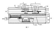
図1に示すように、ディスプレイ組立体は、ディスプレイパネル10と、ディスプレイパネル10の発光面に配置されたフィンガプリント認識モジュール20とを含む。ディスプレイパネル10の発光面は、ディスプレイパネルが画像を表示する側の表面である。ディスプレイパネル10は、有機発光ディスプレイパネル、液晶ディスプレイパネル、またはマイクロダイオードディスプレイパネルのいずれか1つである。図1は、ディスプレイパネルが有機発光ディスプレイパネルである一例のみを示している。ディスプレイパネル10は、基板101、アレイ基板102、ディスプレイ層103、および封止構造体104を含む。この場合、ディスプレイパネル10の発光面は、封止構造体104の側、かつディスプレイ層103から離れた側の外面となる。基板101は、可撓性基板または剛性基板であってもよい。アレイ基板102は複数の画素回路を含み、画素回路における駆動トランジスタ1021のみが図示される。ディスプレイ層103は、画素定義層1031、および複数の発光部品1032を含む。1つの発光部品1032のみが図に示されている。発光部品1032は、順に積層されている、陽極31、発光層32、および陰極33を含む。陽極31は、ビアを介して駆動トランジスタ1021に電気的に接続されている。封止構造体104は、ディスプレイ層103を封止して水および酸素を隔離し、発光部品の寿命を確実にするように構成されている。封止構造体104は、剛性封止であってもよく、封止カバーおよびシール材を含む。代替的に、封止構造体104は、薄膜封止であってもよく、交互に積層された少なくとも1つの有機封止層および少なくとも1つの無機封止層を含む。 As shown in FIG. 1, the display assembly includes a
フィンガプリント認識モジュール20は、複数のフィンガプリント認識ユニットを含み、各フィンガプリント認識ユニットは、少なくとも1つのフォトトランジスタ1と、フォトトランジスタ1に接続された1つのスイッチトランジスタ2とを含む。図には、フィンガプリント認識ユニットが1つだけ示されている。フォトトランジスタ1は、感光要素として使用され、フィンガプリント認識フェーズにおいてフィンガプリント反射光を受け取った後に電気信号に変換し得る。スイッチトランジスタ2は、フォトトランジスタ1に電気的に接続されている。スイッチトランジスタ2は、フィンガプリント電気信号を読み取り、フィンガプリントデータ処理モジュールに出力するように構成されている。最後に、フィンガプリントデータ処理モジュールは、電気信号に対して演算処理を実行し、フィンガプリント情報を生成する。 The
フォトトランジスタ1は、第1の活性層11、第1のゲート12、第1のソース13、および第1のドレイン14を含む。第1の活性層11を作製するための材料は、有機半導体材料を含む。ディスプレイ組立体に垂直な方向では、第1のドレイン14および第1のゲート12が部分的に重なり合って第1のキャパシタCsを形成する。有機半導体材料は、ペンタセン(Pentacene)、6,13ビス(トリイソプロピルシランシルアセチレン)-ペンテン(TIPS-pentacene)、銅フタロシアニン(CuPc)、(ジナフト[2,3-b:2’,3’-f]チエノ[3,2-b]チオフェン)(DNTT)、2,6-ビス(メトキシフェニル)アントラセン(BOPAnt)、ポリ-3-ヘキシルチオフェン(P3HT)、ポリ[ビス(3-ドデシル-2-チエニル)-2,2’-ジチオフェン-5,5’-ジイル](Poly[bis(3-dodecyl-2-thienyl)-2,2’-dithiophene-5,5’-diyl]、PQT-12)、PDVT-10(poly[2,5-bis(alkyl)pyrrolo[3,4-c]-1,4(2H,5H)-dione-alt-5,5’-di(thiophene-2-yl)-2,2’-(E)-2-(2-(thiophen-2-yl)vinyl)thio-phene])、ジケトピロロ-ピロールジチエニルチエノ[3,2-b]チオフェン(DPP-DTT)のいずれか1つ以上のものである。第1の活性層11を製造するとき、溶液法を使用してフィルムを塗布され、その後、エッチング法を使用して第1の活性層11のパターンを形成してもよい。第1の活性層11は、代替的に、蒸着法を使用してフィルムを形成することによって形成してもよい。有機半導体材料は光を強く吸収する。第1の活性層11は、光感知層として使用される。第1の活性層11の表面に光が照射されると、光子が吸収されるたびに第1の活性層11の内部に電子-正孔の対が対応して生成される。電界の作用に起因して、電子および正孔が分離されて電荷キャリアが生成され、電荷キャリアが材料の内部で移動して電流を形成する。これにより、光信号を電気信号に変換することが実装される。異なる有機半導体材料は、異なる光感受性バンドを有する。実際には、フィンガプリント認識は、有機半導体材料の感光帯をフィンガプリント認識光源と一致させることによって実装してもよい。第1の活性層は、可視光に敏感な有機半導体材料、例えば、緑色光に敏感な有機半導体材料を選択し、対応するフィンガプリント認識光源が緑色光を放射するようにする。代替的に、第1の活性層は、赤外光に敏感な有機半導体材料を選択し、対応するフィンガプリント認識光源が赤外光を放射するようにする。
フォトトランジスタ1の動作状態は、暗状態および照明状態を含む。フォトトランジスタ1の暗状態は、第1の活性層11の表面に光が照射されていない状態である。暗状態では、フォトトランジスタ1にバイアス電圧を印加すると、第1の活性層11に小さなリーク電流が生じる。これに対応して、フォトトランジスタ1の照明状態は、第1の活性層11の表面に光が照射された状態である。照明状態では、第1の活性層11には、光励起により生成される小さなリーク電流および光電流が存在する。 The operating states of the
スイッチトランジスタ2は、第2の活性層21、第2のゲート22、第2のソース23、および第2のドレイン24を含む。第2の活性層21を作製する材料は、単結晶シリコン半導体もしくは多結晶シリコン半導体等のシリコン半導体材料であってもよいし、または有機半導体材料であってもよい。第2の活性層21を作製するための材料は、Pentacene、TIPS-pentacene、CuPc、DNTT、BOPAnt、P3HT、PQT-12、PDVT-10、DPP-DTT、2,7-ジオクティ[1]ベンゾチエノ[3、2-B]ベンゾチオフェン(C8-BTBT)、[4,4,9,9-テトラ(4-ヘキシルフェニル)-s-ベンゾジピリジン[1,2-b:5,6-b’]ジチオフェン]-ベンゾチオジアゾール共重合体(C16-IDTBT)、2,8-ジフルオロ-5,11-ビス(トリエチルシリルエチニル)アントラジチオフェン(diF-TES-ADT)、2,9-ジフェニル-ジナフト[2,3-b:2’,3’-f]チエノ[3,2-b]チオフェン(Dph-DNTT)のいずれか1つ以上のものを含む。第2の活性層21および第1の活性層11は同じ材料から作製されてもよいし、または第2の活性層21および第1の活性層11は異なる材料から作製されてもよい。
フィンガプリント認識モジュール20は、第1の金属層41を含む。第1のソース13、第1のドレイン14、第2のソース23、および第2のドレイン24はすべて第1の金属層41に位置し、第1のドレイン14は第2のソース23に接続されている。言い換えれば、ディスプレイ組立体の作製プロセスにおいて、第1のソース13、第1のドレイン14、第2のソース23、および第2のドレイン24を同じエッチング法で製造することにより、プロセスの複雑さを低減してもよい。任意選択で、図1に示すように、第1のドレイン14と第2のソース23とを一体に形成して共通電極を形成し、共通電極の一端が第1のドレイン14として使用され、共通電極の他端が第2のソース23として使用される。
図1に示すように、フィンガプリント認識モジュール20は、第1の活性層11および第2の活性層21の上に不活性化層91をさらに含む。不活性化層91は、絶縁機能および平坦化機能の両方を有していてもよい。ディスプレイ組立体は、フィンガプリント認識モジュール20上に配置された保護カバー92をさらに含む。保護カバー92は、剛性カバーであってもよく、または可撓性カバーであってもよい。任意選択で、耐衝撃層(不図示)が、不活性化層91と保護カバー92との間にさらに配置される。耐衝撃層は、ディスプレイ組立体によって負担される外力を緩衝して、ディスプレイ組立体における各構成要素を外力による損傷から保護し得る。 As shown in FIG. 1 , the
本出願の本実施形態によるディスプレイ組立体は、フィンガプリント認識機能を実装し得る。フィンガプリント認識機能を実装するために必要なフィンガプリント認識光源は、例えば可視光源または赤外光源等の外部光源であってもよい。適用中、外部光源は、ディスプレイパネルの側、かつフィンガプリント認識モジュールから離れた側に配置される。ディスプレイパネルが有機発光ディスプレイパネルであるとき、ディスプレイパネル上の発光部品をフィンガプリント認識光源として再利用してもよい。図2は、発光部品1032がフィンガプリント認識光源として再利用された一例のみを示している。図2に示すように、フィンガプリント認識フェーズでは、ディスプレイパネル10の発光面から発光部品1032が発光した後、フィンガプリント認識モジュール20および保護カバー92を順次透過し、その後、ユーザの指88に照射する。指によって反射された光は保護カバー92を再び透過し、その後、フォトトランジスタ1の第1の活性層に照射される。フィンガプリント反射光を吸収した後、第1の活性層は、光信号を電気信号に変換する。 A display assembly according to this embodiment of the present application may implement fingerprint recognition functionality. The fingerprint recognition light source required to implement the fingerprint recognition function may be an external light source, such as a visible light source or an infrared light source. During application, an external light source is placed on the side of the display panel and away from the fingerprint recognition module. When the display panel is an organic light emitting display panel, the light emitting components on the display panel may be reused as the fingerprint recognition light source. FIG. 2 shows only one example in which the
本出願の本実施形態によるディスプレイ組立体が適用され得るフィンガプリント認識方法では、フィンガプリント認識ユニットの動作プロセスが例として使用される。フィンガプリント認識は、起動フェーズ、初期信号読み取りフェーズ、フィンガプリント信号蓄積フェーズ、およびフィンガプリント信号読み取りフェーズを含む。 In the fingerprint recognition method to which the display assembly according to the present embodiment of the present application may be applied, the operation process of the fingerprint recognition unit is used as an example. Fingerprint recognition includes a startup phase, an initial signal reading phase, a fingerprint signal accumulation phase, and a fingerprint signal reading phase.
起動フェーズにおいて、スイッチトランジスタ2およびフォトトランジスタ1をオフに制御するとき、フォトトランジスタ1は暗状態であり、フォトトランジスタ1のリーク電流は小さい。これにより、フォトトランジスタ1の第1のドレイン14と第1のゲート12との間に形成された第1のキャパシタCsが充電されて、初期電荷量Q0として記録される少量の初期電荷が蓄積される。 In the start-up phase, when switching
初期信号読み取りフェーズにおいて、スイッチトランジスタ2がオンに制御されるとき、スイッチトランジスタ2の第2のソース23および第2のドレイン24が接続されている。第1のドレイン14が第2のソース23に接続されているので、第1のキャパシタCsが放電し、第2のドレイン24を介して初期電荷量Q0が読み取られ、その後、スイッチトランジスタ2がオフに制御される。 In the initial signal reading phase, when the
フィンガプリント信号蓄積フェーズでは、フォトトランジスタ1が指によって反射された光を受け取った後、フォトトランジスタ1は照明状態となり、この光が第1の活性層11に照射され、第1の活性層11内に電荷キャリアが生成される。この場合、フォトトランジスタ1の電流が増加し、第1のキャパシタCsの充電の間に蓄積される電荷量が増加し、フィンガプリント電荷量Q1として記録される。指がディスプレイ組立体の表面を押すとき、指のフィンガプリントの隆線がディスプレイ組立体の表面に直接接するので、フィンガプリント認識光源によって放射された光は、フィンガプリントの隆線がディスプレイ組立体と接するインタフェース上で反射された後、フォトトランジスタ1によって受け取られる。フィンガプリントの谷とディスプレイ組立体の表面との間には空気があるので、フィンガプリント認識光源から放射された光は、ディスプレイ組立体と空気との間のインタフェースを透過した後、フィンガプリントの谷で反射され、その後、再びディスプレイ組立体と空気との間のインタフェースを透過してフォトトランジスタ1で受け取られ得る。したがって、隆線によって反射された光は、谷によって反射された光よりも大きな光強度を有する。これに対応して、フィンガプリント信号蓄積フェーズにおいて、フォトトランジスタが隆線によって反射された光を受け取るときに生成される光電流は、フォトトランジスタが、谷によって反射された光を受け取るときに生成される光電流よりも大きい。この場合、フォトトランジスタが隆線によって反射された光を受け取るとき、第1のキャパシタ上により多くの電荷が蓄積される。したがって、後続の演算処理では、フィンガプリント電荷量の値に基づいて、フィンガプリントの谷とフィンガプリントの隆線とを区別してもよい。 In the fingerprint signal accumulation phase, after the
フィンガプリント信号読取フェーズでは、スイッチトランジスタ2がオンに制御されると、スイッチトランジスタ2の第2のソース23と第2のドレイン24とが再び接続され、第1のキャパシタCsが放電し、第2のドレイン24を介してフィンガプリント電荷量Q1が読み取られる。 In the fingerprint signal reading phase, when the
初期電荷量Q0およびフィンガプリント電荷量Q1をそれぞれ第2のドレインから読み取り、初期電荷量Q0およびフィンガプリント電荷量Q1をフィンガプリントデータ処理モジュール(システムメインボードにおけるモジュール)に転送する。フィンガプリントデータ処理モジュールは、複数のフィンガプリント認識ユニットによって返されたフィンガプリント検出信号を収集して演算処理を実行して、最終的にフィンガプリント情報を生成する。 The initial charge amount Q0 and the fingerprint charge amount Q1 are each read from the second drain, and the initial charge amount Q0 and the fingerprint charge amount Q1 are transferred to a fingerprint data processing module (a module on the system main board). The fingerprint data processing module collects the fingerprint detection signals returned by the plurality of fingerprint recognition units, performs arithmetic processing, and finally generates fingerprint information.
本出願の本実施形態によるディスプレイ組立体によれば、フィンガプリント認識モジュールは、ディスプレイパネルの発光面に配置されている。フィンガプリント認識の間、指によって反射された光は、ディスプレイパネルの構造フィルム層を透過することなしに、フィンガプリント認識モジュールによって受け取られ得る。これにより、フィンガプリント反射光の透過距離を短くし得、フィンガプリント反射光のコリメーションを改善させ、フィンガプリント反射光がディスプレイパネルの構造フィルム層を透過する際の光損失を回避し、フィンガプリント認識精度を改善させ得る。さらに、フォトトランジスタは、フィンガプリント認識モジュールにおける感光要素として使用される。フォトトランジスタの構造は、スイッチトランジスタの構造と同様である。作製中、フォトトランジスタおよびスイッチトランジスタは、作製プロセスの少なくとも一部を共有し得る。これにより、ディスプレイ組立体の構造およびプロセスの複雑さを低減し得、また、ディスプレイ組立体の全体の厚さを低減し得る。 According to the display assembly according to this embodiment of the present application, the fingerprint recognition module is disposed on the light emitting surface of the display panel. During fingerprint recognition, the light reflected by the finger can be received by the fingerprint recognition module without passing through the structural film layer of the display panel. This can shorten the transmission distance of the fingerprint reflected light, improve the collimation of the fingerprint reflected light, avoid light loss when the fingerprint reflected light passes through the structural film layer of the display panel, and improve fingerprint recognition. Accuracy can be improved. Furthermore, phototransistors are used as photosensitive elements in fingerprint recognition modules. The structure of the phototransistor is similar to that of the switch transistor. During fabrication, the phototransistor and switch transistor may share at least a portion of the fabrication process. This may reduce the structural and process complexity of the display assembly and may also reduce the overall thickness of the display assembly.
さらに、感光要素の光感知効果(すなわち、感光効果)は、光電流を暗電流で割ることによって達成され得る大きさのオーダに関係している。すなわち、光電流と暗電流との間の差が大きいほど、光感知効果が良好で、フィンガプリント認識の感度が高いことを示している。ここで、暗電流とは、暗状態(光が照射されていない状態)における感光要素のリーク電流であり、光電流とは、照明状態(光が照射されている状態)において感光要素が光によって励起されたときに生成される電流である。関連技術におけるフィンガプリント認識解決策では、感光要素としてフォトダイオードが使用されており、暗状態のフォトダイオードのリーク電流はnAレベルである。この場合、フォトダイオードの光感知効果を確実にするためには、フォトダイオードの光感知領域を大きくする必要がある。その結果、スイッチトランジスタおよびフォトダイオードを含むフィンガプリント認識モジュールが大きな領域を占める。フィンガプリント認識モジュールをディスプレイパネルの表示面に配置するとき、フィンガプリント認識モジュールはディスプレイパネルから放射される光を大きく遮蔽する。これは表示効果に影響する。しかしながら、本出願の本実施形態では、フォトトランジスタおよびスイッチトランジスタがフィンガプリント認識ユニットを形成する。暗状態におけるフォトトランジスタのリーク電流はpAレベルである。言い換えれば、暗状態におけるフォトトランジスタのリーク電流は、暗状態におけるフォトダイオードのリーク電流よりもはるかに小さい。したがって、本出願におけるフォトトランジスタは、フォトトランジスタのサイズが小さくても良好な光感知効果を有し得る。フォトトランジスタは、ディスプレイパネルの発光面に配置されているので、ディスプレイパネルから放射される光を遮蔽しない。 Furthermore, the light-sensing effect (ie, photosensitive effect) of a photosensitive element is related to the order of magnitude that can be achieved by dividing the photocurrent by the dark current. That is, the larger the difference between the photocurrent and the dark current, the better the light sensing effect and the higher the sensitivity of fingerprint recognition. Here, dark current is the leakage current of the photosensitive element in the dark state (state where no light is irradiated), and photocurrent is the leakage current of the photosensitive element in the illuminated state (state where light is irradiated). This is the current generated when excited. Fingerprint recognition solutions in the related art use photodiodes as photosensitive elements, and the leakage current of the photodiodes in the dark state is at the nA level. In this case, in order to ensure the light sensing effect of the photodiode, it is necessary to increase the light sensing area of the photodiode. As a result, the fingerprint recognition module, including switch transistors and photodiodes, occupies a large area. When the fingerprint recognition module is placed on the display surface of the display panel, the fingerprint recognition module largely blocks the light emitted from the display panel. This will affect the display effect. However, in this embodiment of the present application, the phototransistor and the switch transistor form the fingerprint recognition unit. The leakage current of the phototransistor in the dark state is at the pA level. In other words, the leakage current of the phototransistor in the dark state is much smaller than the leakage current of the photodiode in the dark state. Therefore, the phototransistor in this application can have a good light sensing effect even if the size of the phototransistor is small. Since the phototransistor is placed on the light emitting surface of the display panel, it does not block the light emitted from the display panel.
さらに図1を参照されたい。フィンガプリント認識モジュール20は、第2の金属層42および第1の絶縁層51をさらに含む。第2の金属層42は、第1の金属層41の側、かつディスプレイパネル10に近い側に位置している。第1の絶縁層51は、第1の金属層41と第2の金属層42との間に位置している。第1のゲート12は、第2の金属層42に位置する。すなわち、フォトトランジスタ1の第1のゲート12は、第1の活性層11の側、かつディスプレイパネル10に近い側に位置し、フォトトランジスタ1はボトムゲート構造のトランジスタであり、第1のゲート12は、第1の活性層11に放射される光を遮蔽しない。これにより、フィンガプリント認識フェーズにおいて、フィンガプリント反射光を第1の活性層11に放射し得るので、フォトトランジスタ1は光信号を電気信号に変換することが確実になる。 Please also refer to FIG.
一実施形態では、図1に示すように、スイッチトランジスタ2の第2のゲート22も第2の金属層42に位置する。スイッチトランジスタ2の第2のゲート22とフォトトランジスタ1の第1のゲート12とは、同じ層での同じ材料から作製されてもよい。本実施形態では、スイッチトランジスタとフォトトランジスタとの両方がボトムゲート構造であり、スイッチトランジスタおよびフォトトランジスタとが同じ構造を有するので、スイッチトランジスタおよびフォトトランジスタとを同じプロセスで製造し得る。これにより、フィンガプリント認識精度が改善され、さらに、ディスプレイ組立体の構造およびプロセスの複雑さが低減される。 In one embodiment, the
さらに図1を参照されたい。第1の活性層11と第2の活性層21との両方は、第1の絶縁層51の側、かつ第2の金属層42から離れた側に位置し、第1の絶縁層51と接している。作製プロセスでは、第1のゲート12のパターニングプロセスが完了した後、第1の絶縁層51が第1のゲート12上に製造される。その後、第1の金属層41が第1の絶縁層51上に製造される。そして、第1の金属層41がパターニングされて、第1のソース13、第1のドレイン14、第2のソース23、および第2のドレイン24が形成される。その後、第1の活性層11および第2の活性層21が製造される。第1の活性層11の両端は第1のソース13および第1のドレイン14にそれぞれ接続され、第2の活性層21の両端は第2のソース23および第2のドレイン24にそれぞれ接続されている。第1の活性層11と第2の活性層21との両方が第1の絶縁層51に接しており、これは第1の活性層11および第2の活性層21が同じフィルム層の高さに位置していることと同等である。これは、フィンガプリント認識モジュールのフィルム層の厚さを減少させるのに役立ち、さらに、ディスプレイ組立体の全体の厚さを減少させるのに役立ち得る。 Please also refer to FIG. Both the first
一実施形態では、第1の活性層および第2の活性層が同じ層の同じ材料から作製され、すなわち、第1の活性層のパターンおよび第2の活性層のパターンが同じプロセスで同時に形成される。これにより、プロセスがさらに簡略化され、プロセスの複雑さが軽減され得る。 In one embodiment, the first active layer and the second active layer are made from the same material in the same layer, i.e. the pattern of the first active layer and the pattern of the second active layer are formed simultaneously in the same process. Ru. This may further simplify the process and reduce process complexity.
第2の活性層および第1の活性層が同じ層で同じ材料から作製されているとき、第2の活性層の感光帯は第1の活性層と同じである。これに基づいて、フィンガプリント認識フェーズでのスイッチトランジスタの性能信頼性を確実にするために、本出願の一実施形態は別のディスプレイ組立体を提供する。図3は、本出願の一実施形態によるディスプレイ組立体のフィルム層の部分構造の別の概略図である。第1のソース13、第1のドレイン14、第2のソース23、および第2のドレイン24はすべて第1の金属層41に位置する。第1のゲート12および第2のゲート22はすべて第2の金属層42に位置する。第1の活性層11および第2の活性層21は同じ層の同じ材料から作製され、第1の絶縁層51に接している。フィンガプリント認識モジュール20は、さらに複数の遮光部61(図では1つのみを示す)を含み、1つの遮光部61が1つのスイッチトランジスタ2に対応する。遮光部61は第2の活性層21の側、かつディスプレイパネル10から離れた側にあり、第2の活性層21がある平面上の遮光部61の正投影が第2の活性層21を覆っている。遮光部61を作製するための材料は、金属材料、または有機光吸収材等であってもよい。実際には、第1の活性層において使用される有機半導体材料の感光帯に基づいて、対応する材料を選択して遮光部としてもよい。これにより、遮光部が帯の光を遮蔽することが確実になる。遮光部は光を遮蔽し得、第2の活性層表面への光の照射を防止し、第2の活性層の内部のキャリアを増加させる。これにより、スイッチトランジスタのオン/オフ状態への影響が回避され、フィンガプリント認識検出の精度および性能信頼性が確実になる。 When the second active layer and the first active layer are the same layer and made of the same material, the photosensitive zone of the second active layer is the same as the first active layer. Based on this, one embodiment of the present application provides another display assembly in order to ensure the performance reliability of the switch transistor in the fingerprint recognition phase. FIG. 3 is another schematic diagram of a partial structure of a film layer of a display assembly according to an embodiment of the present application.
任意選択で、フィンガプリント認識フェーズでは、スイッチトランジスタ1がオンになった瞬間に電圧信号が遮光部61を通過するように制御する必要があり、遮光部61をスイッチトランジスタ1のゲートとして使用し得る。したがって、スイッチトランジスタ1はデュアルゲート構造のトランジスタを形成し、スイッチトランジスタ1のターンオン速度を高め得る。 Optionally, in the fingerprint recognition phase, it is necessary to control the voltage signal to pass through the
図3の実施形態によるディスプレイ組立体では、第1の活性層11および第2の活性層21の上に不活性化層91が配置され、さらに遮光部61の上に平坦化層93が配置されている。ディスプレイ組立体はさらに保護カバー92を含む。任意選択で、保護カバー92および平坦化層93上に耐衝撃層(不図示)をさらに配置する。 In the display assembly according to the embodiment of FIG. 3, a
別の実施形態では、第1の活性層と第2の活性層との両方が第1の絶縁層と接しており、第2の活性層および第1の活性層は異なる材料から作製されている。この場合、第2の活性層の感光帯は、第1の活性層の感光帯とは異なる。フィンガプリント認識フェーズでは、フィンガプリント認識光源から放射される光に対して第1の活性層のみが感度を持つ。第2の活性層の表面に照射してさえも、フィンガプリント反射光は第2の活性層に吸収されず、スイッチトランジスタのオン/オフ状態に影響を与える。本実装形態では、光を遮蔽するために第2の活性層に遮光部を配置する必要はない。これにより、遮光部を作製するプロセスがキャンセルされ得る。 In another embodiment, both the first active layer and the second active layer are in contact with the first insulating layer, and the second active layer and the first active layer are made of different materials. . In this case, the photosensitive zone of the second active layer is different from the photosensitive zone of the first active layer. In the fingerprint recognition phase, only the first active layer is sensitive to the light emitted by the fingerprint recognition light source. Even when irradiating the surface of the second active layer, the fingerprint reflected light is not absorbed by the second active layer and affects the on/off state of the switch transistor. In this implementation, there is no need to arrange a light shielding part in the second active layer to shield light. Thereby, the process of creating the light shielding part can be canceled.
別の実施形態では、スイッチトランジスタの第2のゲートとフォトトランジスタの第1のゲートとは異なる金属層に位置する。図4は、本出願の一実施形態によるディスプレイ組立体のフィルム層の部分構造の別の概略図である。第1のソース13、第1のドレイン14、第2のソース23、および第2のドレイン24はすべて第1の金属層41に位置する。第1のゲート12は、第2の金属層42に位置する。第1の活性層11と第2の活性層21との両方は、第1の絶縁層51の側、かつ第2の金属層42から離れた側に位置し、第1の絶縁層51と接している。フィンガプリント認識モジュール20はさらに、第3の金属層43を含む。第3の金属層43は第1の金属層41の側、かつディスプレイパネル10から離れた側にあり、第2のゲート22は第3の金属層43に位置する。絶縁層94は第1の活性層11および第2の活性層21の上に配置され、平坦化層95は第2のゲート22の上に配置される。保護カバー92はさらに平坦化層95上に配置されている。本実装形態では、スイッチトランジスタおよびフォトトランジスタが作製プロセスの一部を共有することが確実にされるように、第1の活性層および第2の活性層を同じ層で同じ材料から作製されてもよい。これにより、作製プロセスの複雑さが軽減される。また、フィンガプリント認識フェーズでは、第2の活性層の側、かつディスプレイパネルから離れた側に配置された第2のゲートを遮光部として再利用し得る。第2のゲートは光を遮蔽し得、フィンガプリント反射光が第2の活性層の表面に照射されるのを防止するので、第2の活性層の内部のキャリアが増加してスイッチトランジスタのオン/オフ状態に影響を与える。これにより、フィンガプリント認識の精度と性能信頼性が確実にされる。 In another embodiment, the second gate of the switch transistor and the first gate of the phototransistor are located in different metal layers. FIG. 4 is another schematic diagram of a partial structure of a film layer of a display assembly according to an embodiment of the present application.
さらに図1を参照されたい。第1のソース13は、第1の絶縁層51上のビア511を介して第1のゲート12に接続されている。すなわち、フォトトランジスタ1の第1のゲート12および第1のソース13が接続され、フォトトランジスタ1は常にオフ状態で動作する。この場合、第1の活性層11の表面に光が照射されないとき、フォトトランジスタ1のリーク電流は非常に小さくなる。しかしながら、フィンガプリント認識フェーズでは、フィンガプリント反射光が第1の活性層11の表面に照射されるとき、第1の活性層の内部で生成されるキャリアにより、フォトトランジスタ1のリーク電流が明らかに増加されるので、フォトトランジスタが高い光感度を有することが確実にされ得る。 Please also refer to FIG. The
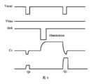
図5は、本出願の一実施形態によるディスプレイ組立体におけるフィンガプリント認識ユニットの回路構造の概略図である。図6は、図5の実施形態におけるフィンガプリント認識回路のシーケンス図である。図5に示すように、フィンガプリント認識モジュールは、フィンガプリント制御信号線71、フィンガプリントデータ信号線72、および第3の電圧信号線73を含む。スイッチトランジスタ2の第2のゲートはフィンガプリント制御信号線71に電気的に接続され、スイッチトランジスタ2の第2のドレインはフィンガプリントデータ信号線72に電気的に接続され、第1のゲート12と第1のソース13との両方が第3の電圧信号線73に電気的に接続されている。なお、本出願の実施形態におけるスイッチトランジスタおよびフォトトランジスタは、スイッチトランジスタおよびフォトトランジスタが同じタイプであることが確実にされれば、p型トランジスタであってもよく、またはn型トランジスタであってもよいことに留意されたい。 FIG. 5 is a schematic diagram of a circuit structure of a fingerprint recognition unit in a display assembly according to an embodiment of the present application. FIG. 6 is a sequence diagram of the fingerprint recognition circuit in the embodiment of FIG. As shown in FIG. 5, the fingerprint recognition module includes a fingerprint
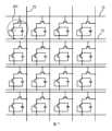
具体的には、フィンガプリント認識モジュールにおける複数のフィンガプリント認識ユニットをアレイ状に配置する。図7は、本出願の一実施形態によるディスプレイ組立体におけるフィンガプリント認識モジュールの回路構造の概略図である。複数のフィンガプリント認識ユニット201がアレイ状に配置される。各フィンガプリント認識ユニット201は、少なくとも1つのフォトトランジスタ1と1つのスイッチトランジスタ2とを含む。同じ行における複数のスイッチトランジスタ2の第2のゲートは1つのフィンガプリント制御信号線71に電気的に接続され、同じ列における複数のスイッチトランジスタ2の第2のドレインは1つのフィンガプリントデータ信号線72に電気的に接続され、同じ行における複数のフォトトランジスタ1の第1のゲート12と第1のソース13とは1つの第3の電圧信号線73に電気的に接続されている。 Specifically, a plurality of fingerprint recognition units in the fingerprint recognition module are arranged in an array. FIG. 7 is a schematic diagram of a circuit structure of a fingerprint recognition module in a display assembly according to an embodiment of the present application. A plurality of
フィンガプリント認識モジュールがスイッチトランジスタおよびフォトダイオードを含む関連技術解決策では、フィンガプリント認識機能を実装するために、電圧信号をスイッチトランジスタのゲート、ソース、およびドレインと、フォトダイオードの1つの電極とに個別に供給する必要があり、そのため駆動回路が複雑になる。しかしながら、本出願の本実施形態では、フィンガプリント認識機能を実装するためには、スイッチトランジスタの第2のゲートおよび第2のドレインと、フォトトランジスタの第1のゲート(または第1のソース)とに電圧信号を入力するだけで済むので、駆動回路が簡単になっている。フィンガプリント認識モジュールに配置する必要があるのは、フィンガプリント制御信号線、フィンガプリントデータ信号線、および第3の電圧信号線の、3タイプの信号線のみである。これにより、フィンガプリント認識モジュールにおける配線方法が簡素化され、配線に占有されるスペースも削減され得る。また、フィンガプリント認識回路はディスプレイパネルを駆動して表示する回路とは独立しており、フィンガプリント認識検出は1フレーム分の画像の走査と時分割で多重化される必要がない。これにより、回路構造の複雑さが軽減される。 In related technology solutions, where the fingerprint recognition module includes a switch transistor and a photodiode, a voltage signal is applied to the gate, source, and drain of the switch transistor and to one electrode of the photodiode to implement the fingerprint recognition function. They must be supplied separately, which complicates the drive circuit. However, in this embodiment of the present application, in order to implement the fingerprint recognition function, the second gate and the second drain of the switch transistor and the first gate (or first source) of the phototransistor are The drive circuit is simplified because it is only necessary to input a voltage signal to the Only three types of signal lines need to be placed in the fingerprint recognition module: a fingerprint control signal line, a fingerprint data signal line, and a third voltage signal line. This simplifies the wiring method in the fingerprint recognition module and can also reduce the space occupied by the wiring. Furthermore, the fingerprint recognition circuit is independent from the circuit that drives the display panel to display images, and the fingerprint recognition and detection need not be multiplexed in time division with the scanning of one frame of images. This reduces the complexity of the circuit structure.
フィンガプリント認識プロセスでは、起動フェーズにおいて、フィンガプリント制御信号線71がフィンガプリント制御信号Vscanをスイッチトランジスタ2に提供し、このフェーズにおいて、フィンガプリント制御信号線71がスイッチトランジスタ2をオフに制御するための無効レベル信号を提供し、フィンガプリントデータ信号線72がスイッチトランジスタ2の第2のドレインに読み取り電位を供給し、フォトトランジスタ1の第1のソースおよび第1のゲートが接続され、第3の電圧信号線73がバイアス電圧Vbiasを供給する。この場合、フォトトランジスタ1はオフ状態、すなわち、暗(dark)状態となり、フォトトランジスタ1のリーク電流の作用の下で、第1のキャパシタCsは充電を開始して少量の電荷を蓄積し、初期電荷量Q0として記録される。初期信号読み取りフェーズでは、フィンガプリント制御信号線71はスイッチトランジスタ2に有効なレベル信号を提供し、スイッチトランジスタ2をオンに制御する。この場合、第1のキャパシタCsが放電し、フィンガプリントデータ信号線72が第2のドレイン24を介して初期電荷量Q0を読み取り、その後、フィンガプリント制御信号線71がスイッチトランジスタ2をオフに制御するための無効レベル信号を提供する。フィンガプリント信号蓄積フェーズでは、フォトトランジスタ1が指によって反射した光を受け取った後、フォトトランジスタ1が暗状態から照明(illumination)状態に変化するので、フォトトランジスタ1のリーク電流が増加する。この場合、第1のキャパシタCsの充電の間に蓄積される電荷量が増加し、フィンガプリント電荷量Q1として記録される。フィンガプリント信号読み取りフェーズでは、フィンガプリント制御信号線71はスイッチトランジスタ2をオンに制御するための有効なレベル信号を提供する。この場合、第1のキャパシタCsは放電し、フィンガプリントデータ信号線72は第2のドレイン24を介してフィンガプリント電荷量Q1を読み取る。 In the fingerprint recognition process, in the startup phase, the fingerprint
具体的には、フィンガプリントデータ信号線72および第2のドレインは同じ金属層に位置しており、すなわち、フィンガプリントデータ信号線72は第1の金属層に位置している(図1に示すフィルム層位置を参照)。この場合、フィンガプリントデータ信号線72および第2のドレインは同じプロセスで製造されてもよく、フィンガプリントデータ信号線72および第2のドレインは絶縁層のビアを介して接続する必要はない。これにより、プロセスが簡略化される。フィンガプリント制御信号線71および第2のゲートは同じ金属層に位置し、フィンガプリント制御信号線71および第2のゲートは同じ作製プロセスにおいて製造され、フィンガプリント制御信号線71および第2のゲートは絶縁層のビアを介して接続する必要はない。これにより、作製プロセスが簡略化される。さらに、第3の電圧信号線73は、第1のゲートと同じ金属層に位置してもよく、または第1のソースと同じ金属層に位置してもよい。 Specifically, the fingerprint data signal
一実施形態では、フィンガプリントデータ信号線および第2のドレインは第1の金属層に位置し、フィンガプリント制御信号線および第2のゲートは第3の金属層に位置し、第3の電圧信号線および第1のゲートは第2の金属層に位置する。フィンガプリントデータ信号線、フィンガプリント制御信号線、および第3の電圧信号線は、3つの異なる金属層で個別に配線されている。これにより、各金属層の配線密度が低減され得る。 In one embodiment, the fingerprint data signal line and the second drain are located on the first metal layer, the fingerprint control signal line and the second gate are located on the third metal layer, and the fingerprint control signal line and the second gate are located on the third metal layer. The line and the first gate are located in the second metal layer. The fingerprint data signal line, the fingerprint control signal line, and the third voltage signal line are individually routed in three different metal layers. Thereby, the wiring density of each metal layer can be reduced.
別の実施形態では、図8は、本出願の実施形態によるディスプレイ組立体のフィルム層の部分構造の別の概略図である。ディスプレイパネルは有機発光ディスプレイパネルである。図8に示すように、ディスプレイパネルは、順次配置されている、基板101、アレイ基板102、ディスプレイ層103、および封止構造体104を含む。アレイ基板102は、ゲート金属層44、キャパシタ金属層(不図示)、ソース/ドレイン金属層45、および第4の金属層46を含む。絶縁層は隣接する2つの金属層の間に配置される。駆動トランジスタ1021のゲート66とディスプレイパネルのゲート走査線69(図にのみ示されている)とが、ゲート金属層44に位置する。駆動トランジスタ1021のソース67およびドレイン68と、ディスプレイパネルのデータ線とが、ソース/ドレイン金属層45に位置する。画素回路のキャパシタプレートとディスプレイパネルのリセット信号線とは、キャパシタ金属層に位置している。ディスプレイパネルにおいて正の電力信号線は、第4の金属層46に位置している。任意選択で、フィンガプリント認識モジュール20におけるスイッチトランジスタ2の第2のゲート22をゲート走査線69に接続されている。図は、第2のゲート22が少なくとも1つの接続電極461を介してゲート走査線69に電気的に接続されていることを示している。任意選択で、接続電極461は第4の金属層46に配置される。第2のゲート22は、封止構造体104およびディスプレイ層103を透過するビア77を介して接続電極461に電気的に接続され、接続電極461は、絶縁層上のビア78を介してゲート走査線69に電気的に接続されている。言い換えれば、フィンガプリント認識フェーズでは、ゲート走査線69は、フィンガプリント制御信号線として再利用され、制御信号は、ゲート走査線69を介してスイッチトランジスタ2に供給される。さらに、フィンガプリント認識モジュールにおけるスイッチトランジスタ2の第2のドレイン24は、ソース/ドレイン金属層45にあるデータ線に電気的に接続されていてもよく、そのデータ線はフィンガプリント認識フェーズでフィンガプリントデータ信号線として再利用される。フィンガプリント認識モジュールにおけるフォトトランジスタ1の第1のゲート12は、第4の金属層46の正電力信号線に電気的に接続されていてもよく、正電力信号線はフィンガプリント認識フェーズにおいて第3の電圧信号線として再利用される。本実装形態では、アレイ基板内にあり、かつディスプレイパネルを表示するために駆動する線が、フィンガプリント認識モジュールにおける信号線として再利用される。ディスプレイ駆動時系列とフィンガプリント認識時系列とが互いに連携することで、ディスプレイ機能とフィンガプリント認識機能との両方を実装できる。 In another embodiment, FIG. 8 is another schematic diagram of a substructure of a film layer of a display assembly according to an embodiment of the present application. The display panel is an organic light emitting display panel. As shown in FIG. 8, the display panel includes a
別の実施形態では、第1のソースおよび第1のゲートは接続されておらず、フィンガプリント認識フェーズでは、第1のソースに供給される電圧の値と第1のゲートに供給される電圧の値とを個別に制御することによって、フォトトランジスタがオフ状態で動作するように制御される。図9は、本出願の一実施形態によるディスプレイ組立体のフィルム層の部分構造の別の概略図である。図10は、図9の一実施形態によるフィンガプリント認識ユニットの回路構成の概略図である。 In another embodiment, the first source and the first gate are not connected, and in the fingerprint recognition phase, the value of the voltage supplied to the first source and the voltage supplied to the first gate are By individually controlling the values, the phototransistor is controlled to operate in the off state. FIG. 9 is another schematic diagram of a partial structure of a film layer of a display assembly according to an embodiment of the present application. FIG. 10 is a schematic diagram of a circuit configuration of a fingerprint recognition unit according to an embodiment of FIG.
図9に示すように、ディスプレイパネル10が有機発光ディスプレイパネルであることは依然として例として使用されており、フィンガプリント認識モジュール20はディスプレイパネル10の発光面に位置している。フィンガプリント認識モジュール20は、複数のフィンガプリント認識ユニットを含む。各フィンガプリント認識ユニットは、少なくとも1つのフォトトランジスタ1と1つのスイッチトランジスタ2とを含む。フォトトランジスタ1は、第1の活性層11、第1のゲート12、第1のソース13、および第1のドレイン14を含む。第1の活性層11を作製するための材料は、有機半導体材料を含む。第1のドレイン14および第1のゲート12は部分的に重なり合って、第1のキャパシタCsを形成する。スイッチトランジスタ2は、第2の活性層21、第2のゲート22、第2のソース23、および第2のドレイン24を含む。第1のドレイン14は第2のソース23に接続されている。図1の実施形態と異なり、図9の実施形態では、第1のソース13および第1のゲート12は接続されていない。 As shown in FIG. 9, it is still used as an example that the
図10に示すように、フィンガプリント認識モジュールは、フィンガプリント制御信号線71、フィンガプリントデータ信号線72、第1の電圧信号線74、および第2の電圧信号線75を含む。第2のゲートはフィンガプリント制御信号線71に電気的に接続され、第2のドレインはフィンガプリントデータ信号線72に電気的に接続され、第1のゲートは第1の電圧信号線74に電気的に接続され、第1のソースは第2の電圧信号線75に電気的に接続されている。フィンガプリント認識フェーズでは、第1の電圧信号線74が第1のゲートに供給する電圧は、第2の電圧信号線75が第1のソースに供給する電圧よりも大きい。したがって、第1の電圧信号線74が第1のゲートに電圧信号を供給し、第2の電圧信号線75が第1のソースに電圧信号を供給するとき、フォトトランジスタ1はオフ状態に制御され得る。 As shown in FIG. 10, the fingerprint recognition module includes a fingerprint
本実装形態では、フィンガプリント認識ユニットの動作プロセスは、図5および図6の前述の実施形態を参照して理解してもよく、詳細は本明細書では再度説明しない。 In this implementation, the operational process of the fingerprint recognition unit may be understood with reference to the previous embodiments of FIGS. 5 and 6, and the details will not be described again herein.
さらに、図11は、本出願の一実施形態による部分ディスプレイ組立体の概略上面図である。図11に示すように、ディスプレイパネル10は表示領域55および非表示領域56を含み、表示領域55は複数の画素領域111と、隣接する画素領域111同士の間に位置する非画素領域121とを含む。画素領域111は画素発光領域であり、非画素領域121は非発光領域である。有機発光ディスプレイパネルが例として使用されている画素領域111は発光部品が位置する領域であり、非画素領域121は発光部品から離間した画素定義層が位置する領域である。液晶ディスプレイパネルが例として使用されている液晶ディスプレイパネルはブラックマトリクスを含み、ブラックマトリクスは複数の開口部を含む。開口部によって露出される領域が画素領域111であり、隣接する開口部の間の領域が非画素領域である。ディスプレイパネル10上のフィンガプリント認識ユニット201の正投影は、非画素領域121に位置している。フィンガプリント認識ユニット201のディスプレイパネル10への正投影方向は、上方視点方向と同じである。したがって、上方視点方向では、フィンガプリント認識ユニット201は、フィンガプリント認識ユニット201のディスプレイパネル10への正投影と一致する。上方視点では、フィンガプリント認識ユニット201は、フィンガプリント認識ユニット201のディスプレイパネル10への正投影を表している。図11は、フィンガプリント認識ユニット201が一部の固定領域にのみ配置されていることを示している。任意選択で、代替的に、フィンガプリント認識ユニットが、対応する表示領域の全面に配置されてもよい。本実装形態では、フィンガプリント認識ユニットはディスプレイパネルの非画素領域に対応する。ディスプレイ組立体が表示されるとき、フィンガプリント認識ユニットは画素領域の発光を遮蔽しないので、フィンガプリント認識モジュールの堆積が表示効果に影響しないことが確実にされる。 Additionally, FIG. 11 is a schematic top view of a partial display assembly according to one embodiment of the present application. As shown in FIG. 11, the
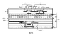
すべての前述の実施形態では、ディスプレイパネルが有機発光ディスプレイパネルである一例を使用して説明する。本出願の本実施形態で提供されるディスプレイ組立体では、ディスプレイパネルはまた、液晶ディスプレイパネルであってもよい。詳細については、図12を参照されたい。図12は、本出願の一実施形態によるディスプレイ組立体のフィルム層の部分構造の別の概略図である。ディスプレイパネル10は、順に積層されている、基板101、アレイ基板105、液晶分子層106、およびカラーフィルタ基板107を含む。アレイ基板105は、複数の画素回路を含む。図では、画素回路の駆動トランジスタ1051のみを例として使用されている。アレイ基板は、画素電極1052および共通電極1053をさらに含む。駆動トランジスタ1051は画素電極1052に接続されている。図中の画素電極1052および共通電極1053の相対位置は入れ替えてもよい。カラーフィルタ基板107は、クロマトグラフィー層およびブラックマトリクスを含む。フィンガプリント認識モジュールはディスプレイパネルに位置する。フィンガプリント認識モジュール20はフィンガプリント認識ユニットを含み、フィンガプリント認識ユニットは少なくとも1つのフォトトランジスタ1と1つのスイッチトランジスタ2とを含む。フィンガプリント認識モジュールにおけるフォトトランジスタ1の構造およびスイッチトランジスタ2の構造については、前述の各実施形態のいずれか1つにおける説明を参照されたい。詳細は本明細書では再度説明しない。 All of the above embodiments are described using an example in which the display panel is an organic light emitting display panel. In the display assembly provided in this embodiment of the present application, the display panel may also be a liquid crystal display panel. Please refer to FIG. 12 for details. FIG. 12 is another schematic diagram of a partial structure of a film layer of a display assembly according to an embodiment of the present application. The
同じ発明概念に基づいて、本出願の一実施形態はディスプレイ装置をさらに提供する。図13は、本出願の一実施形態によるディスプレイ装置の概略図である。図13に示すように、ディスプレイ装置は、本出願のいずれかの実施形態で提供されるディスプレイ組立体100を含む。ディスプレイ組立体100の具体的な構造については前述の実施形態で詳細に説明してきており、詳細については本明細書では再度説明しない。もちろん、図13のディスプレイ装置は説明のための一例にすぎない。ディスプレイ装置は、携帯電話、タブレットコンピュータ、ノートパソコン、電子書籍、またはテレビ等の、フィンガプリント認識機能を有する任意の電子機器であってもよい。ディスプレイ装置は、剛体ディスプレイ装置であってもよく、または可撓性ディスプレイ装置もしくは折りたたみ可能なディスプレイ装置であってもよい。一実施形態では、ディスプレイパネル上の画素ユニットは、フィンガプリント認識フェーズにおけるフィンガプリント認識の光源として再利用される。別の実施形態では、ディスプレイ装置はフィンガプリント認識光源を含む。フィンガプリント認識光源は、ディスプレイパネル側、かつフィンガプリント認識モジュールから離れた側にある。フィンガプリント認識光源は、赤外線光源であってもよく、または可視光源であってもよい。 Based on the same inventive concept, an embodiment of the present application further provides a display device. FIG. 13 is a schematic diagram of a display device according to an embodiment of the present application. As shown in FIG. 13, a display device includes a
前述の説明は、本発明の特定の実装形態にすぎず、本発明の保護範囲を限定することは意図されていない。本発明に開示されている技術的範囲内で当業者によって容易に考え出されるいかなる変形または置換も、本発明の保護範囲内にあるものとする。したがって、本発明の保護範囲は、特許請求の範囲の保護範囲に従うものとする。 The above descriptions are only specific implementations of the present invention and are not intended to limit the protection scope of the present invention. Any modification or replacement easily figured out by a person skilled in the art within the technical scope disclosed in the present invention shall fall within the protection scope of the present invention. Therefore, the protection scope of the present invention shall be subject to the protection scope of the claims.
1 フォトトランジスタ、スイッチトランジスタ
2 スイッチトランジスタ
10 ディスプレイパネル
11 第1の活性層
12 第1のゲート
13 第1のソース
14 第1のドレイン
20 フィンガプリント認識モジュール
21 第2の活性層
22 第2のゲート
23 第2のソース
24 第2のドレイン
31 陽極
32 発光層
33 陰極
41 第1の金属層
42 第2の金属層
43 第3の金属層
44 ゲート金属層
45 ソース/ドレイン金属層
46 第4の金属層
51 第1の絶縁層
55 表示領域
56 非表示領域
61 遮光部
66 ゲート
67 ソース
68 ドレイン
69 ゲート走査線
71 フィンガプリント制御信号線
72 フィンガプリントデータ信号線
73 第3の電圧信号線
74 第1の電圧信号線
75 第2の電圧信号線
77 ビア
78 ビア
88 ユーザの指
91 不活性化層
92 保護カバー
93 平坦化層
94 絶縁層
95 平坦化層
100 ディスプレイ組立体
101 基板
102 アレイ基板
103 ディスプレイ層
104 封止構造体
105 アレイ基板
106 液晶分子層
107 カラーフィルタ基板
111 画素領域
121 非画素領域
201 フィンガプリント認識ユニット
461 接続電極
511 ビア
1021 駆動トランジスタ
1031 画素定義層
1032 発光部品
1051 駆動トランジスタ
1052 画素電極
1053 共通電極1 Phototransistor,
Claims (13)
Translated fromJapanese前記フォトトランジスタが、第1の活性層、第1のゲート、第1のソース、および第1のドレインを備え、前記第1の活性層を作製する材料が、有機半導体材料を含み、前記ディスプレイ組立体に垂直な方向において、前記第1のドレインおよび前記第1のゲートが部分的に重なり合って第1のキャパシタを形成し、
前記スイッチトランジスタが、第2の活性層、第2のゲート、第2のソース、および第2のドレインを備え、
前記フィンガプリント認識モジュールが、第1の金属層を備え、前記第1のソース、前記第1のドレイン、前記第2のソース、および前記第2のドレインが、すべて前記第1の金属層に位置し、前記第1のドレインが、前記第2のソースに接続され、
前記第1の活性層が、前記第1のゲートの少なくとも一部の上方に配置され、前記第1の活性層が、前記第1のソース及び前記第1のドレインの少なくとも一部の上方であって、前記第1のソース及び前記第1のドレインの少なくとも一部を覆うように配置される、
ディスプレイ組立体。A display assembly comprising a display panel and a fingerprint recognition module located on a light emitting surface of the display panel, the fingerprint recognition module comprising a plurality of fingerprint recognition units, each fingerprint recognition unit comprising: comprising at least one phototransistor and one switch transistor,
the phototransistor comprises a first active layer, a first gate, a first source, and a first drain, the material of which the first active layer is made includes an organic semiconductor material; the first drain and the first gate partially overlap in a direction perpendicular to the three-dimensional space to form a first capacitor;
the switch transistor includes a second active layer, a second gate, a second source, and a second drain;
the fingerprint recognition module comprises a first metal layer, the first source, the first drain, the second source, and the second drain all located in the first metal layer; and the first drainis connected to the second source,
The first active layer is disposed above at least a portion of the first gate, and the first active layer is above at least a portion of the first source and the first drain. arranged to cover at least a portion of the first source and the first drain;
display assembly.
前記第1のゲートが、前記第2の金属層に位置する、
請求項1に記載のディスプレイ組立体。The fingerprint recognition module further includes a second metal layer and a first insulating layer, the second metal layer being located on a side of the first metal layer and closer to the display panel, and one insulating layer located between the first metal layer and the second metal layer,
the first gate is located in the second metal layer;
A display assembly according to claim 1.
請求項2に記載のディスプレイ組立体。Both the first active layer and the second active layer are located on the side of the first insulating layer and away from the second metal layer, and are in contact with the first insulating layer. ing,
A display assembly according to claim 2.
前記第2のゲートが、前記フィンガプリント制御信号線に電気的に接続され、前記第2のドレインが、前記フィンガプリントデータ信号線に電気的に接続され、前記第1のゲートが、前記第1の電圧信号線に電気的に接続され、前記第1のソースが、前記第2の電圧信号線に電気的に接続され、
フィンガプリント認識フェーズにおいて、前記第1の電圧信号線によって前記第1のゲートに供給される電圧が、前記第2の電圧信号線によって前記第1のソースに供給される電圧よりも大きい、
請求項2に記載のディスプレイ組立体。the fingerprint recognition module includes a fingerprint control signal line, a fingerprint data signal line, a first voltage signal line, and a second voltage signal line;
The second gate is electrically connected to the fingerprint control signal line, the second drain is electrically connected to the fingerprint data signal line, and the first gate is electrically connected to the fingerprint control signal line. the first source is electrically connected to the second voltage signal line, and the first source is electrically connected to the second voltage signal line;
in the fingerprint recognition phase, the voltage supplied to the first gate by the first voltage signal line is greater than the voltage supplied to the first source by the second voltage signal line;
A display assembly according to claim 2.
請求項2に記載のディスプレイ組立体。the first source is connected to the first gate via a via in the first insulating layer;
A display assembly according to claim 2.
前記第2のゲートが、前記フィンガプリント制御信号線に電気的に接続され、前記第2のドレインが、前記フィンガプリントデータ信号線に電気的に接続され、前記第1のゲートと前記第1のソースとの両方が前記第3の電圧信号線に電気的に接続されている、
請求項5に記載のディスプレイ組立体。the fingerprint recognition module includes a fingerprint control signal line, a fingerprint data signal line, and a third voltage signal line;
The second gate is electrically connected to the fingerprint control signal line, the second drain is electrically connected to the fingerprint data signal line, and the first gate and the first and a source are electrically connected to the third voltage signal line,
A display assembly according to claim 5.
請求項2に記載のディスプレイ組立体。the second gate is located in the second metal layer;
A display assembly according to claim 2.
請求項7に記載のディスプレイ組立体。the second active layer and the first active layer are made of the same material in the same layer;
A display assembly according to claim 7.
請求項8に記載のディスプレイ組立体。The fingerprint recognition module further includes a plurality of light shielding parts, and the light shielding parts are located on a side of the second active layer and away from the display panel, and the second active layer is located on a side of the fingerprint recognition module. an orthographic projection of the light shielding portion on a plane covers the second active layer;
A display assembly according to claim 8.
請求項1に記載のディスプレイ組立体。The fingerprint recognition module further includes a third metal layer, the third metal layer is located on a side of the first metal layer and away from the display panel, and the second gate is located on the side of the first metal layer and away from the display panel. located in the third metal layer,
A display assembly according to claim 1.
前記ディスプレイパネル上の前記フィンガプリント認識ユニットの正投影が前記非画素領域に位置する、
請求項1に記載のディスプレイ組立体。The display panel includes a plurality of pixel regions and a non-pixel region located between the adjacent pixel regions,
an orthographic projection of the fingerprint recognition unit on the display panel is located in the non-pixel area;
A display assembly according to claim 1.
前記スイッチトランジスタと前記フォトトランジスタとの両方をオフに制御し、前記フォトトランジスタのリーク電流の作用下で前記第1のキャパシタに初期電荷量を蓄積するように充電するステップと、
前記スイッチトランジスタをオンに制御し、前記第1のキャパシタを放電し、前記第2のドレインを通して前記初期電荷量を読み取った後に前記スイッチトランジスタをオフに制御するステップと、
前記フォトトランジスタが指によって反射された光を受け取った後、前記リーク電流を増加させ、前記第1のキャパシタにフィンガプリント電荷量を蓄積するように充電するステップと、
前記スイッチトランジスタをオンに制御し、前記第1のキャパシタを放電し、前記第2のドレインを通して前記フィンガプリント電荷量を読み取るステップと
を含む、フィンガプリント認識方法。12. A fingerprint recognition method applicable to a display assembly according to any one of claims 1 to 11, the fingerprint recognition method comprising:
controlling both the switch transistor and the phototransistor to turn off and charging the first capacitor to accumulate an initial charge amount under the action of the leakage current of the phototransistor;
controlling the switch transistor to turn on, discharging the first capacitor, and controlling the switch transistor to turn off after reading the initial charge amount through the second drain;
increasing the leakage current and charging the first capacitor to accumulate a fingerprint charge after the phototransistor receives light reflected by a finger;
controlling the switch transistor on, discharging the first capacitor, and reading the amount of fingerprint charge through the second drain.
Applications Claiming Priority (3)
| Application Number | Priority Date | Filing Date | Title |
|---|---|---|---|
| CN202010246037.8 | 2020-03-31 | ||
| CN202010246037.8ACN113471249B (en) | 2020-03-31 | 2020-03-31 | Display component, display device and fingerprint recognition method |
| PCT/CN2021/082248WO2021197118A1 (en) | 2020-03-31 | 2021-03-23 | Display assembly, display device, and fingerprint recognition method |
Publications (2)
| Publication Number | Publication Date |
|---|---|
| JP2023519994A JP2023519994A (en) | 2023-05-15 |
| JP7407967B2true JP7407967B2 (en) | 2024-01-04 |
Family
ID=77865675
Family Applications (1)
| Application Number | Title | Priority Date | Filing Date |
|---|---|---|---|
| JP2022559713AActiveJP7407967B2 (en) | 2020-03-31 | 2021-03-23 | Display assembly, display device, and fingerprint recognition method |
Country Status (5)
| Country | Link |
|---|---|
| US (1) | US20230144932A1 (en) |
| EP (1) | EP4116877B1 (en) |
| JP (1) | JP7407967B2 (en) |
| CN (2) | CN119212488A (en) |
| WO (1) | WO2021197118A1 (en) |
Families Citing this family (4)
| Publication number | Priority date | Publication date | Assignee | Title |
|---|---|---|---|---|
| EP4163818A4 (en)* | 2020-06-09 | 2024-07-03 | Wuhan China Star Optoelectronics Technology Co., Ltd. | Optical fingerprint recognition circuit and display panel |
| CN113990906A (en)* | 2021-10-27 | 2022-01-28 | 京东方科技集团股份有限公司 | Display substrate, pattern recognition method thereof, and display device |
| CN115909424A (en)* | 2022-11-23 | 2023-04-04 | 武汉华星光电半导体显示技术有限公司 | Display panel |
| WO2025109913A1 (en)* | 2023-11-20 | 2025-05-30 | ソニーセミコンダクタソリューションズ株式会社 | Semiconductor device and electronic equipment |
Citations (7)
| Publication number | Priority date | Publication date | Assignee | Title |
|---|---|---|---|---|
| JP2006503333A (en) | 2002-10-17 | 2006-01-26 | サムスン エレクトロニクス カンパニー リミテッド | Integrated liquid crystal display device with a fingerprint recognition element and manufacturing method thereof |
| JP2007310628A (en) | 2006-05-18 | 2007-11-29 | Hitachi Displays Ltd | Image display device |
| WO2011125353A1 (en) | 2010-04-07 | 2011-10-13 | シャープ株式会社 | Circuit board, display device, and method for manufacturing circuit board |
| JP2015159133A (en) | 2012-06-14 | 2015-09-03 | シャープ株式会社 | Receiver |
| JP2016095886A (en) | 2009-08-24 | 2016-05-26 | 株式会社半導体エネルギー研究所 | Display device |
| US20180173349A1 (en) | 2016-12-16 | 2018-06-21 | Samsung Display Co., Ltd. | Display panel and display device including the same |
| JP2019165129A (en) | 2018-03-20 | 2019-09-26 | 株式会社ジャパンディスプレイ | Optical sensor device, and display device |
Family Cites Families (12)
| Publication number | Priority date | Publication date | Assignee | Title |
|---|---|---|---|---|
| US8319299B2 (en)* | 2009-11-20 | 2012-11-27 | Auman Brian C | Thin film transistor compositions, and methods relating thereto |
| CN104850292B (en)* | 2015-06-01 | 2017-09-29 | 京东方科技集团股份有限公司 | A kind of In-cell touch panel, its driving method and display device |
| CN105184247B (en)* | 2015-08-28 | 2018-12-28 | 京东方科技集团股份有限公司 | A kind of fingerprint recognition element, its recognition methods, display device and display device |
| CN106096595B (en)* | 2016-08-08 | 2022-08-09 | 京东方科技集团股份有限公司 | Fingerprint identification module, manufacturing method thereof and fingerprint identification display device |
| CN106326845B (en)* | 2016-08-15 | 2017-08-11 | 京东方科技集团股份有限公司 | Fingerprint identification unit and preparation method, array base palte, display device and fingerprint identification method |
| KR101981318B1 (en)* | 2017-04-19 | 2019-05-23 | 크루셜텍(주) | Transparent Fingerprint Image Scanning Panel and Display Apparatus Comprising The Same |
| CN107425041B (en)* | 2017-07-27 | 2020-01-31 | 上海天马微电子有限公司 | touch display panel, device and manufacturing method |
| CN109656048B (en)* | 2019-01-10 | 2022-02-15 | 昆山龙腾光电股份有限公司 | Liquid crystal display device having a plurality of pixel electrodes |
| CN109614963B (en)* | 2019-01-28 | 2023-08-29 | 京东方科技集团股份有限公司 | Fingerprint identification structure and display device |
| CN110008885B (en)* | 2019-03-29 | 2021-04-30 | 厦门天马微电子有限公司 | Display panel and display device |
| CN110286796B (en)* | 2019-06-27 | 2023-10-27 | 京东方科技集团股份有限公司 | Electronic substrate, manufacturing method thereof and display panel |
| US20210149249A1 (en)* | 2019-11-19 | 2021-05-20 | Shenzhen China Star Optoelectronics Semiconductor Display Technology Co., Ltd. | Display device |
- 2020
- 2020-03-31CNCN202411187691.0Apatent/CN119212488A/enactivePending
- 2020-03-31CNCN202010246037.8Apatent/CN113471249B/enactiveActive
- 2021
- 2021-03-23USUS17/915,909patent/US20230144932A1/enactivePending
- 2021-03-23WOPCT/CN2021/082248patent/WO2021197118A1/ennot_activeCeased
- 2021-03-23EPEP21780145.5Apatent/EP4116877B1/enactiveActive
- 2021-03-23JPJP2022559713Apatent/JP7407967B2/enactiveActive
Patent Citations (7)
| Publication number | Priority date | Publication date | Assignee | Title |
|---|---|---|---|---|
| JP2006503333A (en) | 2002-10-17 | 2006-01-26 | サムスン エレクトロニクス カンパニー リミテッド | Integrated liquid crystal display device with a fingerprint recognition element and manufacturing method thereof |
| JP2007310628A (en) | 2006-05-18 | 2007-11-29 | Hitachi Displays Ltd | Image display device |
| JP2016095886A (en) | 2009-08-24 | 2016-05-26 | 株式会社半導体エネルギー研究所 | Display device |
| WO2011125353A1 (en) | 2010-04-07 | 2011-10-13 | シャープ株式会社 | Circuit board, display device, and method for manufacturing circuit board |
| JP2015159133A (en) | 2012-06-14 | 2015-09-03 | シャープ株式会社 | Receiver |
| US20180173349A1 (en) | 2016-12-16 | 2018-06-21 | Samsung Display Co., Ltd. | Display panel and display device including the same |
| JP2019165129A (en) | 2018-03-20 | 2019-09-26 | 株式会社ジャパンディスプレイ | Optical sensor device, and display device |
Also Published As
| Publication number | Publication date |
|---|---|
| EP4116877B1 (en) | 2024-07-31 |
| CN113471249B (en) | 2024-09-20 |
| CN119212488A (en) | 2024-12-27 |
| EP4116877A4 (en) | 2023-07-26 |
| CN113471249A (en) | 2021-10-01 |
| EP4116877A1 (en) | 2023-01-11 |
| US20230144932A1 (en) | 2023-05-11 |
| WO2021197118A1 (en) | 2021-10-07 |
| JP2023519994A (en) | 2023-05-15 |
Similar Documents
| Publication | Publication Date | Title |
|---|---|---|
| JP7407967B2 (en) | Display assembly, display device, and fingerprint recognition method | |
| CN112055893B (en) | Display panel and manufacturing method thereof | |
| US12379798B2 (en) | Display assembly, display apparatus, and driving method | |
| US8399821B2 (en) | Light source integrated photoelectric conversion apparatus | |
| KR101230316B1 (en) | Display device and manufacturing method of the same | |
| WO2017188715A2 (en) | Light-emitting fingerprint recognition panel capable of applying under glass and fingerprint recognition display apparatus comprising same | |
| KR20160051687A (en) | Solid-state imaging element, production method thereof, and electronic device | |
| US20220123083A1 (en) | Display substrate, display panel and display device | |
| US20210082989A1 (en) | Photoelectric conversion element, imaging device, and electronic apparatus | |
| JP7515255B2 (en) | Flat panel detector and method of manufacturing same | |
| TWI877138B (en) | Image-sensor matrix-array device comprising thin-film transistors and organic photodiodes | |
| US20230309346A1 (en) | Imaging device, display apparatus, and method for manufacturing display apparatus | |
| CN112616321A (en) | Display substrate, manufacturing method thereof and display device | |
| KR20230061348A (en) | Image display devices and electronic devices | |
| KR102866806B1 (en) | Display device | |
| CN117716408A (en) | display device | |
| US20240407225A1 (en) | Display apparatus | |
| US20240185633A1 (en) | Electronic device and authentication method of electronic device | |
| US20250275411A1 (en) | Light emitting device | |
| KR20250144362A (en) | Display device | |
| WO2022229779A1 (en) | Display device, display module, and electronic apparatus | |
| CN117915723A (en) | Display panel, detection circuit and display device | |
| CN118234303A (en) | Display panel and display terminal | |
| KR20240159737A (en) | Display device |
Legal Events
| Date | Code | Title | Description |
|---|---|---|---|
| A621 | Written request for application examination | Free format text:JAPANESE INTERMEDIATE CODE: A621 Effective date:20221109 | |
| A977 | Report on retrieval | Free format text:JAPANESE INTERMEDIATE CODE: A971007 Effective date:20230921 | |
| A131 | Notification of reasons for refusal | Free format text:JAPANESE INTERMEDIATE CODE: A131 Effective date:20231002 | |
| A521 | Request for written amendment filed | Free format text:JAPANESE INTERMEDIATE CODE: A523 Effective date:20231122 | |
| TRDD | Decision of grant or rejection written | ||
| A01 | Written decision to grant a patent or to grant a registration (utility model) | Free format text:JAPANESE INTERMEDIATE CODE: A01 Effective date:20231204 | |
| A61 | First payment of annual fees (during grant procedure) | Free format text:JAPANESE INTERMEDIATE CODE: A61 Effective date:20231219 | |
| R150 | Certificate of patent or registration of utility model | Ref document number:7407967 Country of ref document:JP Free format text:JAPANESE INTERMEDIATE CODE: R150 |