JP7407752B2 - wafer support stand - Google Patents
wafer support standDownload PDFInfo
- Publication number
- JP7407752B2 JP7407752B2JP2021017029AJP2021017029AJP7407752B2JP 7407752 B2JP7407752 B2JP 7407752B2JP 2021017029 AJP2021017029 AJP 2021017029AJP 2021017029 AJP2021017029 AJP 2021017029AJP 7407752 B2JP7407752 B2JP 7407752B2
- Authority
- JP
- Japan
- Prior art keywords
- heater
- heaters
- wafer
- ceramic base
- jumper
- Prior art date
- Legal status (The legal status is an assumption and is not a legal conclusion. Google has not performed a legal analysis and makes no representation as to the accuracy of the status listed.)
- Active
Links
- 239000000919ceramicSubstances0.000claimsdescription25
- 230000015572biosynthetic processEffects0.000claimsdescription14
- 230000005611electricityEffects0.000claimsdescription7
- 238000010586diagramMethods0.000description2
- 230000002093peripheral effectEffects0.000description2
- 230000003247decreasing effectEffects0.000description1
- 230000012447hatchingEffects0.000description1
- 238000010438heat treatmentMethods0.000description1
- 238000004519manufacturing processMethods0.000description1
- 238000000034methodMethods0.000description1
- 238000005268plasma chemical vapour depositionMethods0.000description1
Images

Classifications
- H—ELECTRICITY
- H01—ELECTRIC ELEMENTS
- H01J—ELECTRIC DISCHARGE TUBES OR DISCHARGE LAMPS
- H01J37/00—Discharge tubes with provision for introducing objects or material to be exposed to the discharge, e.g. for the purpose of examination or processing thereof
- H01J37/32—Gas-filled discharge tubes
- H01J37/32431—Constructional details of the reactor
- H01J37/32715—Workpiece holder
- H—ELECTRICITY
- H01—ELECTRIC ELEMENTS
- H01L—SEMICONDUCTOR DEVICES NOT COVERED BY CLASS H10
- H01L21/00—Processes or apparatus adapted for the manufacture or treatment of semiconductor or solid state devices or of parts thereof
- H01L21/67—Apparatus specially adapted for handling semiconductor or electric solid state devices during manufacture or treatment thereof; Apparatus specially adapted for handling wafers during manufacture or treatment of semiconductor or electric solid state devices or components ; Apparatus not specifically provided for elsewhere
- H01L21/67005—Apparatus not specifically provided for elsewhere
- H01L21/67011—Apparatus for manufacture or treatment
- H01L21/67098—Apparatus for thermal treatment
- H01L21/67103—Apparatus for thermal treatment mainly by conduction
- H—ELECTRICITY
- H01—ELECTRIC ELEMENTS
- H01J—ELECTRIC DISCHARGE TUBES OR DISCHARGE LAMPS
- H01J37/00—Discharge tubes with provision for introducing objects or material to be exposed to the discharge, e.g. for the purpose of examination or processing thereof
- H01J37/02—Details
- H01J37/20—Means for supporting or positioning the object or the material; Means for adjusting diaphragms or lenses associated with the support
- H—ELECTRICITY
- H01—ELECTRIC ELEMENTS
- H01J—ELECTRIC DISCHARGE TUBES OR DISCHARGE LAMPS
- H01J37/00—Discharge tubes with provision for introducing objects or material to be exposed to the discharge, e.g. for the purpose of examination or processing thereof
- H01J37/32—Gas-filled discharge tubes
- H01J37/32431—Constructional details of the reactor
- H01J37/32715—Workpiece holder
- H01J37/32724—Temperature
- H—ELECTRICITY
- H01—ELECTRIC ELEMENTS
- H01L—SEMICONDUCTOR DEVICES NOT COVERED BY CLASS H10
- H01L21/00—Processes or apparatus adapted for the manufacture or treatment of semiconductor or solid state devices or of parts thereof
- H01L21/67—Apparatus specially adapted for handling semiconductor or electric solid state devices during manufacture or treatment thereof; Apparatus specially adapted for handling wafers during manufacture or treatment of semiconductor or electric solid state devices or components ; Apparatus not specifically provided for elsewhere
- H01L21/67005—Apparatus not specifically provided for elsewhere
- H01L21/67011—Apparatus for manufacture or treatment
- H01L21/67098—Apparatus for thermal treatment
- H—ELECTRICITY
- H01—ELECTRIC ELEMENTS
- H01L—SEMICONDUCTOR DEVICES NOT COVERED BY CLASS H10
- H01L21/00—Processes or apparatus adapted for the manufacture or treatment of semiconductor or solid state devices or of parts thereof
- H01L21/67—Apparatus specially adapted for handling semiconductor or electric solid state devices during manufacture or treatment thereof; Apparatus specially adapted for handling wafers during manufacture or treatment of semiconductor or electric solid state devices or components ; Apparatus not specifically provided for elsewhere
- H01L21/67005—Apparatus not specifically provided for elsewhere
- H01L21/67242—Apparatus for monitoring, sorting or marking
- H01L21/67248—Temperature monitoring
- H—ELECTRICITY
- H01—ELECTRIC ELEMENTS
- H01L—SEMICONDUCTOR DEVICES NOT COVERED BY CLASS H10
- H01L21/00—Processes or apparatus adapted for the manufacture or treatment of semiconductor or solid state devices or of parts thereof
- H01L21/67—Apparatus specially adapted for handling semiconductor or electric solid state devices during manufacture or treatment thereof; Apparatus specially adapted for handling wafers during manufacture or treatment of semiconductor or electric solid state devices or components ; Apparatus not specifically provided for elsewhere
- H01L21/683—Apparatus specially adapted for handling semiconductor or electric solid state devices during manufacture or treatment thereof; Apparatus specially adapted for handling wafers during manufacture or treatment of semiconductor or electric solid state devices or components ; Apparatus not specifically provided for elsewhere for supporting or gripping
- H01L21/687—Apparatus specially adapted for handling semiconductor or electric solid state devices during manufacture or treatment thereof; Apparatus specially adapted for handling wafers during manufacture or treatment of semiconductor or electric solid state devices or components ; Apparatus not specifically provided for elsewhere for supporting or gripping using mechanical means, e.g. chucks, clamps or pinches
- H01L21/68714—Apparatus specially adapted for handling semiconductor or electric solid state devices during manufacture or treatment thereof; Apparatus specially adapted for handling wafers during manufacture or treatment of semiconductor or electric solid state devices or components ; Apparatus not specifically provided for elsewhere for supporting or gripping using mechanical means, e.g. chucks, clamps or pinches the wafers being placed on a susceptor, stage or support
- H01L21/68757—Apparatus specially adapted for handling semiconductor or electric solid state devices during manufacture or treatment thereof; Apparatus specially adapted for handling wafers during manufacture or treatment of semiconductor or electric solid state devices or components ; Apparatus not specifically provided for elsewhere for supporting or gripping using mechanical means, e.g. chucks, clamps or pinches the wafers being placed on a susceptor, stage or support characterised by a coating or a hardness or a material
- H—ELECTRICITY
- H01—ELECTRIC ELEMENTS
- H01L—SEMICONDUCTOR DEVICES NOT COVERED BY CLASS H10
- H01L21/00—Processes or apparatus adapted for the manufacture or treatment of semiconductor or solid state devices or of parts thereof
- H01L21/67—Apparatus specially adapted for handling semiconductor or electric solid state devices during manufacture or treatment thereof; Apparatus specially adapted for handling wafers during manufacture or treatment of semiconductor or electric solid state devices or components ; Apparatus not specifically provided for elsewhere
- H01L21/683—Apparatus specially adapted for handling semiconductor or electric solid state devices during manufacture or treatment thereof; Apparatus specially adapted for handling wafers during manufacture or treatment of semiconductor or electric solid state devices or components ; Apparatus not specifically provided for elsewhere for supporting or gripping
- H01L21/687—Apparatus specially adapted for handling semiconductor or electric solid state devices during manufacture or treatment thereof; Apparatus specially adapted for handling wafers during manufacture or treatment of semiconductor or electric solid state devices or components ; Apparatus not specifically provided for elsewhere for supporting or gripping using mechanical means, e.g. chucks, clamps or pinches
- H01L21/68714—Apparatus specially adapted for handling semiconductor or electric solid state devices during manufacture or treatment thereof; Apparatus specially adapted for handling wafers during manufacture or treatment of semiconductor or electric solid state devices or components ; Apparatus not specifically provided for elsewhere for supporting or gripping using mechanical means, e.g. chucks, clamps or pinches the wafers being placed on a susceptor, stage or support
- H01L21/68785—Apparatus specially adapted for handling semiconductor or electric solid state devices during manufacture or treatment thereof; Apparatus specially adapted for handling wafers during manufacture or treatment of semiconductor or electric solid state devices or components ; Apparatus not specifically provided for elsewhere for supporting or gripping using mechanical means, e.g. chucks, clamps or pinches the wafers being placed on a susceptor, stage or support characterised by the mechanical construction of the susceptor, stage or support
- H—ELECTRICITY
- H01—ELECTRIC ELEMENTS
- H01L—SEMICONDUCTOR DEVICES NOT COVERED BY CLASS H10
- H01L21/00—Processes or apparatus adapted for the manufacture or treatment of semiconductor or solid state devices or of parts thereof
- H01L21/67—Apparatus specially adapted for handling semiconductor or electric solid state devices during manufacture or treatment thereof; Apparatus specially adapted for handling wafers during manufacture or treatment of semiconductor or electric solid state devices or components ; Apparatus not specifically provided for elsewhere
- H01L21/683—Apparatus specially adapted for handling semiconductor or electric solid state devices during manufacture or treatment thereof; Apparatus specially adapted for handling wafers during manufacture or treatment of semiconductor or electric solid state devices or components ; Apparatus not specifically provided for elsewhere for supporting or gripping
- H01L21/687—Apparatus specially adapted for handling semiconductor or electric solid state devices during manufacture or treatment thereof; Apparatus specially adapted for handling wafers during manufacture or treatment of semiconductor or electric solid state devices or components ; Apparatus not specifically provided for elsewhere for supporting or gripping using mechanical means, e.g. chucks, clamps or pinches
- H01L21/68714—Apparatus specially adapted for handling semiconductor or electric solid state devices during manufacture or treatment thereof; Apparatus specially adapted for handling wafers during manufacture or treatment of semiconductor or electric solid state devices or components ; Apparatus not specifically provided for elsewhere for supporting or gripping using mechanical means, e.g. chucks, clamps or pinches the wafers being placed on a susceptor, stage or support
- H01L21/68792—Apparatus specially adapted for handling semiconductor or electric solid state devices during manufacture or treatment thereof; Apparatus specially adapted for handling wafers during manufacture or treatment of semiconductor or electric solid state devices or components ; Apparatus not specifically provided for elsewhere for supporting or gripping using mechanical means, e.g. chucks, clamps or pinches the wafers being placed on a susceptor, stage or support characterised by the construction of the shaft
- H—ELECTRICITY
- H05—ELECTRIC TECHNIQUES NOT OTHERWISE PROVIDED FOR
- H05B—ELECTRIC HEATING; ELECTRIC LIGHT SOURCES NOT OTHERWISE PROVIDED FOR; CIRCUIT ARRANGEMENTS FOR ELECTRIC LIGHT SOURCES, IN GENERAL
- H05B3/00—Ohmic-resistance heating
- H05B3/02—Details
- H05B3/03—Electrodes
- H—ELECTRICITY
- H05—ELECTRIC TECHNIQUES NOT OTHERWISE PROVIDED FOR
- H05B—ELECTRIC HEATING; ELECTRIC LIGHT SOURCES NOT OTHERWISE PROVIDED FOR; CIRCUIT ARRANGEMENTS FOR ELECTRIC LIGHT SOURCES, IN GENERAL
- H05B3/00—Ohmic-resistance heating
- H05B3/10—Heating elements characterised by the composition or nature of the materials or by the arrangement of the conductor
- H—ELECTRICITY
- H05—ELECTRIC TECHNIQUES NOT OTHERWISE PROVIDED FOR
- H05B—ELECTRIC HEATING; ELECTRIC LIGHT SOURCES NOT OTHERWISE PROVIDED FOR; CIRCUIT ARRANGEMENTS FOR ELECTRIC LIGHT SOURCES, IN GENERAL
- H05B3/00—Ohmic-resistance heating
- H05B3/20—Heating elements having extended surface area substantially in a two-dimensional plane, e.g. plate-heater
- H05B3/22—Heating elements having extended surface area substantially in a two-dimensional plane, e.g. plate-heater non-flexible
- H05B3/26—Heating elements having extended surface area substantially in a two-dimensional plane, e.g. plate-heater non-flexible heating conductor mounted on insulating base
- H05B3/265—Heating elements having extended surface area substantially in a two-dimensional plane, e.g. plate-heater non-flexible heating conductor mounted on insulating base the insulating base being an inorganic material, e.g. ceramic
- H—ELECTRICITY
- H05—ELECTRIC TECHNIQUES NOT OTHERWISE PROVIDED FOR
- H05B—ELECTRIC HEATING; ELECTRIC LIGHT SOURCES NOT OTHERWISE PROVIDED FOR; CIRCUIT ARRANGEMENTS FOR ELECTRIC LIGHT SOURCES, IN GENERAL
- H05B3/00—Ohmic-resistance heating
- H05B3/20—Heating elements having extended surface area substantially in a two-dimensional plane, e.g. plate-heater
- H05B3/22—Heating elements having extended surface area substantially in a two-dimensional plane, e.g. plate-heater non-flexible
- H05B3/28—Heating elements having extended surface area substantially in a two-dimensional plane, e.g. plate-heater non-flexible heating conductor embedded in insulating material
- H05B3/283—Heating elements having extended surface area substantially in a two-dimensional plane, e.g. plate-heater non-flexible heating conductor embedded in insulating material the insulating material being an inorganic material, e.g. ceramic
- H—ELECTRICITY
- H05—ELECTRIC TECHNIQUES NOT OTHERWISE PROVIDED FOR
- H05B—ELECTRIC HEATING; ELECTRIC LIGHT SOURCES NOT OTHERWISE PROVIDED FOR; CIRCUIT ARRANGEMENTS FOR ELECTRIC LIGHT SOURCES, IN GENERAL
- H05B2203/00—Aspects relating to Ohmic resistive heating covered by group H05B3/00
- H05B2203/002—Heaters using a particular layout for the resistive material or resistive elements
- H05B2203/007—Heaters using a particular layout for the resistive material or resistive elements using multiple electrically connected resistive elements or resistive zones
- H—ELECTRICITY
- H05—ELECTRIC TECHNIQUES NOT OTHERWISE PROVIDED FOR
- H05B—ELECTRIC HEATING; ELECTRIC LIGHT SOURCES NOT OTHERWISE PROVIDED FOR; CIRCUIT ARRANGEMENTS FOR ELECTRIC LIGHT SOURCES, IN GENERAL
- H05B2203/00—Aspects relating to Ohmic resistive heating covered by group H05B3/00
- H05B2203/014—Heaters using resistive wires or cables not provided for in H05B3/54
- H—ELECTRICITY
- H05—ELECTRIC TECHNIQUES NOT OTHERWISE PROVIDED FOR
- H05B—ELECTRIC HEATING; ELECTRIC LIGHT SOURCES NOT OTHERWISE PROVIDED FOR; CIRCUIT ARRANGEMENTS FOR ELECTRIC LIGHT SOURCES, IN GENERAL
- H05B2203/00—Aspects relating to Ohmic resistive heating covered by group H05B3/00
- H05B2203/017—Manufacturing methods or apparatus for heaters
Landscapes
- Engineering & Computer Science (AREA)
- Physics & Mathematics (AREA)
- Microelectronics & Electronic Packaging (AREA)
- Condensed Matter Physics & Semiconductors (AREA)
- General Physics & Mathematics (AREA)
- Manufacturing & Machinery (AREA)
- Computer Hardware Design (AREA)
- Power Engineering (AREA)
- Chemical & Material Sciences (AREA)
- Analytical Chemistry (AREA)
- Ceramic Engineering (AREA)
- Plasma & Fusion (AREA)
- Inorganic Chemistry (AREA)
- Container, Conveyance, Adherence, Positioning, Of Wafer (AREA)
Description
Translated fromJapanese本発明は、ウエハ支持台に関する。 The present invention relates to a wafer support.
従来、ウエハにプラズマCVDによる成膜処理等を行う際に用いられるセラミック製のウエハ支持台であって、ウエハ加熱に用いるヒータが多層に配置されたものが知られている。例えば、特許文献1には電気的に独立した多層のヒータが記載されている。 2. Description of the Related Art Conventionally, a ceramic wafer support stand used when a wafer is subjected to a film forming process by plasma CVD, etc., is known in which heaters used for heating the wafer are arranged in multiple layers. For example, Patent Document 1 describes an electrically independent multilayer heater.
しかしながら、このようなウエハ支持台はシャフトからの抜熱により中心部の温度が低下することは防ぐことができるが、ウエハ支持台の外周からの影響によって均熱性が悪化するおそれがあった。 However, although such a wafer support can prevent the temperature at the center from decreasing due to heat removal from the shaft, there is a risk that thermal uniformity may deteriorate due to influence from the outer periphery of the wafer support.
本発明はこのような課題を解決するためになされたものであり、ウエハの外周部での均熱性を改善することを主目的とする。 The present invention has been made to solve these problems, and its main purpose is to improve the thermal uniformity at the outer periphery of the wafer.
本発明のウエハ支持台は、
ウエハ載置面を有するセラミック基体と、
前記セラミック基体に埋設された複数のヒータと、
を備え、
前記セラミック基体は、前記ウエハ載置面から前記ウエハ載置面とは反対側の面に向かって、第1ヒータ形成面、前記第2ヒータ形成面及び前記第3ヒータ形成面をこの順に有し、
前記複数のヒータは、前記第1ヒータ形成面に設けられた第1ヒータ、前記第2ヒータ形成面に設けられた第2ヒータ及び前記第3ヒータ形成面に設けられた第3ヒータを含み、
前記第1ヒータは、前記セラミック基体の中心に位置するように設けられ、
前記第2ヒータは、前記第1ヒータの外周に位置するように設けられ、
前記第3ヒータは、前記第2ヒータに重なるように設けられ、前記第3ヒータ形成面が半径方向の線分によって複数に分割されたゾーンのそれぞれに設けられている、
ものである。The wafer support stand of the present invention includes:
a ceramic base having a wafer mounting surface;
a plurality of heaters embedded in the ceramic base;
Equipped with
The ceramic base has a first heater formation surface, a second heater formation surface, and a third heater formation surface in this order from the wafer placement surface toward a surface opposite to the wafer placement surface. ,
The plurality of heaters include a first heater provided on the first heater formation surface, a second heater provided on the second heater formation surface, and a third heater provided on the third heater formation surface,
the first heater is provided so as to be located at the center of the ceramic base,
the second heater is provided so as to be located on the outer periphery of the first heater,
The third heater is provided to overlap the second heater, and is provided in each zone in which the third heater forming surface is divided into a plurality of zones by a line segment in a radial direction.
It is something.
本発明のウエハ支持台では、第3ヒータ形成面が半径方向の線分によって複数に分割されたゾーンのそれぞれに第3ヒータを有するため、複数の第3ヒータを個別に温度制御することができ、それによって、外周部要因による均熱性への影響を抑制することができる。また、第1ヒータを他のヒータの形成面と異なりよりウエハ載置面に近くに埋設することにより、他のヒータのジャンパ線が通ることが無く、第1ヒータの設計自由度が高くなり均熱性が向上する。 In the wafer support table of the present invention, since the third heater forming surface has the third heater in each zone divided into a plurality of zones by line segments in the radial direction, the temperature of the plurality of third heaters can be individually controlled. , Thereby, it is possible to suppress the influence on thermal uniformity due to peripheral factors. In addition, by burying the first heater closer to the wafer mounting surface than the other heater formation surfaces, jumper wires of other heaters do not pass through, increasing the degree of freedom in designing the first heater and making it more uniform. Improves thermal properties.
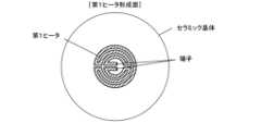
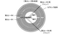
本発明の好適な実施形態を、図面を参照しながら以下に説明する。図1はプラズマ発生装置に用いられるウエハ支持台の断面図、図2はコイル状のヒータとジャンパとの関係を示す説明図、図3~図5はセラミック基体の第1~第3ヒータ形成面の平面図である。図3~図5ではコイル状のヒータをハッチングで示した。 Preferred embodiments of the present invention will be described below with reference to the drawings. FIG. 1 is a cross-sectional view of a wafer support used in a plasma generator, FIG. 2 is an explanatory diagram showing the relationship between a coiled heater and a jumper, and FIGS. 3 to 5 are first to third heater forming surfaces of a ceramic base. FIG. In FIGS. 3 to 5, coil-shaped heaters are shown by hatching.
ウエハ支持台は、ウエハ載置面を有するセラミック基体と、セラミック基体に埋設された複数のヒータと、セラミック基体のウエハ載置面とは反対側の面に設けられた筒状のシャフトとを備える。 The wafer support table includes a ceramic base having a wafer mounting surface, a plurality of heaters embedded in the ceramic base, and a cylindrical shaft provided on a surface of the ceramic base opposite to the wafer mounting surface. .
セラミック基体は、ウエハ載置面からウエハ載置面とは反対側の面に向かって、第1ヒータ形成面、第2ヒータ形成面及び第3ヒータ形成面をこの順に有する。 The ceramic base has a first heater forming surface, a second heater forming surface, and a third heater forming surface in this order from the wafer mounting surface toward the surface opposite to the wafer mounting surface.
複数のヒータは、第1ヒータ形成面に設けられた第1ヒータ、第2ヒータ形成面に設けられた第2ヒータ(第2ヒータX,Y)及び第3ヒータ形成面に設けられた第3ヒータ(第3ヒータA~D)を含む。第1ヒータは、セラミック基体の中心に位置するように設けられている。 The plurality of heaters include a first heater provided on the first heater forming surface, a second heater (second heaters X, Y) provided on the second heater forming surface, and a third heater provided on the third heater forming surface. Contains heaters (third heaters A to D). The first heater is provided so as to be located at the center of the ceramic base.
第1ヒータは、一方の端子から一筆書きの要領で他方の端子に至るようにコイルを配線したものである。 The first heater has a coil wired from one terminal to the other terminal in a single stroke.
第2ヒータは、第2ヒータ形成面の内側に設けられた第2ヒータXと、第2ヒータ形成面の外側に設けられた第2ヒータYとを備える。第2ヒータX,Yは、いずれも第1ヒータの外周に位置するように設けられている。第2ヒータXは、一方の端子から一方の第2ヒータX用ジャンパによって第1ヒータの外側に引き出されたあと、一筆書きの要領でコイルが配線され、他方の第2ヒータX用ジャンパによって中心側の他方の端子に引き込まれている。第2ヒータYは、一方の端子から一方の第2ヒータY用ジャンパによって第2ヒータXの外側に引き出されたあと、一筆書きの要領でコイルが配線され、他方の第2ヒータY用ジャンパによって中心側の他方の端子に引き込まれている。第2ヒータX,Y用ジャンパは、第2ヒータ形成面に設けられている。つまり、第2ヒータX,Y用ジャンパは、第2ヒータX,Yと同一面に形成されている。なお、同一面とは、第2ヒータX,Yの高さと重複する面であればよい。例えば、第2ヒータX,Yがコイル状の場合、ウエハ載置面に最も近いコイル上部とウエハ載置面から最も遠いコイル下部の間であれば、同一面である(以下同じ)。 The second heater includes a second heater X provided inside the second heater forming surface and a second heater Y provided outside the second heater forming surface. The second heaters X and Y are both provided so as to be located on the outer periphery of the first heater. The second heater It is pulled into the other terminal on the side. The second heater Y is pulled out from one terminal to the outside of the second heater It is pulled into the other terminal on the center side. Jumpers for the second heaters X and Y are provided on the second heater forming surface. That is, the jumper for the second heaters X and Y is formed on the same surface as the second heaters X and Y. Note that the same surface may be a surface that overlaps the height of the second heaters X and Y. For example, when the second heaters X and Y are coil-shaped, the upper part of the coil closest to the wafer mounting surface and the lower part of the coil furthest from the wafer mounting surface are on the same surface (the same applies hereinafter).
第3ヒータは、4つの第3ヒータA~Dを備える。第3ヒータA~Dは、第3ヒータ形成面が半径方向の線分によって複数(図5では4つ)に分割されたゾーンのそれぞれに設けられ、平面視でいずれも第2ヒータと重なっている。ここでは、第3ヒータAと第3ヒータBとは、一体化されている。具体的には、第3ヒータAは、一方の端子から第3ヒータA用ジャンパによって外側に引き出されたあと、一筆書きの要領でコイルが配線されて第3ヒータA,B用共通ジャンパ(グランド端子に接続される)の接続部に至る。第3ヒータBは、その接続部から一筆書きの要領でコイルが配線されたあと第3ヒータB用ジャンパによって中心側の他方の端子に引き込まれている。また、第3ヒータCと第3ヒータDとは、一体化されている。具体的には、第3ヒータCは、一方の端子から第3ヒータC用ジャンパによって外側に引き出されたあと、一筆書きの要領でコイルが配線されて第3ヒータC,D用共通ジャンパ(グランド端子に接続される)の接続部に至る。第3ヒータDは、その接続部から一筆書きの要領でコイルが配線されたあと第3ヒータD用ジャンパによって中心側の他方の端子に引き込まれている。第3ヒータA,B用ジャンパと、第3ヒータA,B用共通ジャンパと、第3ヒータC,D用ジャンパと、第3ヒータC,D用共通ジャンパは、いずれも第3ヒータA~Dと同様、第3ヒータ形成面に設けられている、つまり、これらのジャンパは、第3ヒータA~Dと同一面に形成されている。 The third heater includes four third heaters A to D. The third heaters A to D are provided in each zone in which the third heater forming surface is divided into a plurality of zones (four in FIG. 5) by line segments in the radial direction, and all overlap with the second heater in a plan view. There is. Here, the third heater A and the third heater B are integrated. Specifically, the third heater A is pulled out from one terminal by the jumper for the third heater A, and then the coil is wired in a single stroke and connected to the common jumper (ground) for the third heaters A and B. (connected to the terminal). The third heater B has a coil wired from its connection part in a single-stroke manner, and then is drawn into the other terminal on the center side by a jumper for the third heater B. Further, the third heater C and the third heater D are integrated. Specifically, the third heater C is pulled out from one terminal by the jumper for the third heater C, and then the coil is wired in a single stroke and connected to the common jumper (ground) for the third heaters C and D. (connected to the terminal). The third heater D has a coil wired from its connecting portion in a single stroke manner, and then is drawn into the other terminal on the center side by a jumper for the third heater D. The jumper for third heaters A and B, the common jumper for third heaters A and B, the jumper for third heaters C and D, and the common jumper for third heaters C and D are all for third heaters A to D. Similarly, these jumpers are provided on the third heater forming surface, that is, these jumpers are formed on the same surface as the third heaters A to D.
セラミック基体には、ウエハ載置面とは反対側の面から、第1ヒータ、第2ヒータ(第2ヒータX,Y)および第3ヒータ(第3ヒータA~D)のそれぞれに対応する端子に向かって端子穴が形成されている。第1ヒータ、第2ヒータ(第2ヒータX,Y)および第3ヒータ(第3ヒータA~D)に対応する端子穴は、各ヒータの深さに比例して深くなっている。 The ceramic base is provided with terminals corresponding to the first heater, the second heater (second heaters X, Y), and the third heater (third heaters A to D) from the surface opposite to the wafer mounting surface. A terminal hole is formed towards the end. The terminal holes corresponding to the first heater, the second heater (second heaters X, Y), and the third heater (third heaters A to D) become deeper in proportion to the depth of each heater.
第1ヒータ、第2ヒータ(第2ヒータX,Y)および第3ヒータ(第3ヒータA~D)は上述したようにコイル形状である。第2ヒータ用ジャンパは、第2ヒータのコイルのうちウエハ載置面から反対側の面側に位置するコイル下部に接続されている。第3ヒータ用ジャンパは、第3ヒータのコイルのうちウエハ載置面側に位置するコイル上部に接続されている。 The first heater, the second heater (second heaters X, Y), and the third heater (third heaters A to D) have a coil shape as described above. The second heater jumper is connected to a lower portion of the coil of the second heater located on the side opposite to the wafer mounting surface. The third heater jumper is connected to the upper part of the coil of the third heater, which is located on the wafer mounting surface side.
セラミック基体は、第1ヒータよりもウエハ載置面側にRF電極を有する。第1ヒータに電気を供給するロッドと、第2ヒータ(第2ヒータX,Y)に電気を供給するロッドと、第3ヒータ(第3ヒータA~D)に電気を供給するロッドと、RF電極に接続されたロッドは、シャフトから下方へ突出した部分の長さがすべて同じである。 The ceramic base has an RF electrode closer to the wafer mounting surface than the first heater. A rod that supplies electricity to the first heater, a rod that supplies electricity to the second heater (second heaters X, Y), a rod that supplies electricity to the third heater (third heaters A to D), and an RF The rods connected to the electrodes all have the same length that project downward from the shaft.
第2ヒータは、第2ヒータ形成面がセラミック基体と同心円状の境界によって複数(ここでは2つ)に分割されたゾーンのそれぞれに設けられている。 The second heater is provided in each of zones in which the second heater forming surface is divided into a plurality of zones (in this case, two zones) by boundaries concentric with the ceramic base.
以上説明した本実施形態のウエハ支持台では、第3ヒータ形成面が半径方向の線分によって複数に分割されたゾーンのそれぞれに第3ヒータA~Dを有するため、複数の第3ヒータA~Dを個別に温度制御することができ、それによって、外周部要因による均熱性への影響を抑制することができる。また、第1ヒータを他のヒータの形成面と異なりよりウエハ載置面の近くに埋設することにより、他のヒータのジャンパ線が通ることが無く、第1ヒータの設計自由度が高くなり均熱性が向上する。 In the wafer support table of the present embodiment described above, the third heater forming surface has the third heaters A to D in each of the zones divided into a plurality of zones by line segments in the radial direction. The temperature of D can be individually controlled, thereby suppressing the influence of peripheral factors on thermal uniformity. In addition, by burying the first heater closer to the wafer mounting surface than the other heater formation surfaces, jumper wires of other heaters do not pass through, increasing the degree of freedom in designing the first heater and making it more uniform. Improves thermal properties.
また、環状の第2ヒータと扇状の第3ヒータとが重なっているため、より精密な温度制御が可能になる。 Moreover, since the annular second heater and the fan-shaped third heater overlap, more precise temperature control is possible.
更に、第1ヒータ、第2ヒータ(第2ヒータX,Y)および第3ヒータ(第3ヒータA~D)に対応する端子穴は、各ヒータの深さに比例して深くなっている。そのため、セラミック基体の厚さ方向に延びるジャンパがなく、製造が容易となる。 Further, the terminal holes corresponding to the first heater, the second heater (second heaters X, Y), and the third heater (third heaters A to D) are deepened in proportion to the depth of each heater. Therefore, there is no jumper extending in the thickness direction of the ceramic base, making manufacturing easy.
更にまた、第2ヒータのコイル中心よりもウエハ載置面とは反対側の面側(本実施形態ではコイル下部)から第2ヒータ用ジャンパを引き出しているため、ウエハ載置面からジャンパまでの距離D1(図2参照)を大きくすることができ、ジャンパの発熱による影響を小さくすることができる。 Furthermore, since the jumper for the second heater is pulled out from the side opposite to the wafer mounting surface from the center of the coil of the second heater (the lower part of the coil in this embodiment), the distance from the wafer mounting surface to the jumper is The distance D1 (see FIG. 2) can be increased, and the influence of heat generated by the jumper can be reduced.
そしてまた、第3ヒータのコイル中心よりもウエハ載置面側(本実施形態ではコイル上部)から第3ヒータ用ジャンパを引き出しているため、セラミック基体のウエハ載置面とは反対側の面からジャンパまでの距離D2(図2参照)を長くすることができる。これにより、端子を取り付ける穴の長さを確保することができる。 Furthermore, since the jumper for the third heater is pulled out from the wafer mounting surface side (the upper part of the coil in this embodiment) from the center of the coil of the third heater, the third heater jumper is pulled out from the side of the ceramic base opposite to the wafer mounting surface. The distance D2 (see FIG. 2) to the jumper can be increased. Thereby, the length of the hole for attaching the terminal can be ensured.
そして更に、複数のヒータおよびRF電極に電力を供給するロッドがシャフトから出る長さがそろっているため、ロッド受け側の構造を簡略化することができる。 Furthermore, since the rods that supply power to the plurality of heaters and RF electrodes extend from the shaft at the same length, the structure on the rod receiving side can be simplified.
Claims (6)
Translated fromJapanese前記セラミック基体に埋設された複数のヒータと、
を備え、
前記セラミック基体は、前記ウエハ載置面から前記ウエハ載置面とは反対側の面に向かって、第1ヒータ形成面、第2ヒータ形成面及び第3ヒータ形成面をこの順に有し、
前記複数のヒータは、前記第1ヒータ形成面に設けられた第1ヒータ、前記第2ヒータ形成面に設けられた第2ヒータ及び前記第3ヒータ形成面に設けられた第3ヒータを含み、
前記第1ヒータは、前記セラミック基体の中心に位置するように設けられ、
前記第2ヒータは、前記第1ヒータの外周に位置するように設けられ、
前記第3ヒータは、平面視で前記第2ヒータに重なるように設けられ、前記第3ヒータ形成面が半径方向の線分によって複数に分割されたゾーンのそれぞれに設けられている、
ウエハ支持台。a ceramic base having a wafer mounting surface;
a plurality of heaters embedded in the ceramic base;
Equipped with
The ceramic base has a first heater formation surface, a second heater formation surface,and a third heater formation surface in this order from the wafer placement surface toward the surface opposite to the wafer placement surface,
The plurality of heaters include a first heater provided on the first heater formation surface, a second heater provided on the second heater formation surface, and a third heater provided on the third heater formation surface,
the first heater is provided so as to be located at the center of the ceramic base,
the second heater is provided so as to be located on the outer periphery of the first heater,
The third heater is provided so as to overlap the second heaterin a plan view , and is provided in each zone in which the third heater forming surface is divided into a plurality of zones by a line segment in a radial direction.
Wafer support.
第3ヒータ用ジャンパは、前記第3ヒータ形成面に設けられている、
請求項1に記載のウエハ支持台。a second heater jumper is provided on the second heater forming surface;
A third heaterjumper is provided on the third heater forming surface,
The wafer support stand according to claim 1.
前記第3ヒータ用ジャンパは、前記第3ヒータのコイル中心よりも前記ウエハ載置面側に接続されている、
請求項2に記載のウエハ支持台。The first heater, the second heater, and the third heater arecoil -shaped, and thesecond heater jumper is located on the side opposite to the wafer mounting surface from the coil center of the second heater. connected,
The third heaterjumperis connected to the wafer mounting surface side of the coil center of the third heater.
The wafer support stand according to claim2 .
請求項1~3のいずれか1項に記載のウエハ支持台。 The wafer support stand according to any one of claims 1 to 3.
前記第1ヒータに電気を供給するロッドと、前記第2ヒータに電気を供給するロッドと、前記第3ヒータに電気を供給するロッドと、前記RF電極に接続されたロッドは、前記シャフトから突出した部分の長さがすべて同じである、
請求項1~4のいずれか1項に記載のウエハ支持台。The ceramic base has an RF electrode closer to the wafer mounting surface than the plurality of heaters, and has a cylindrical shaft on a surface opposite to the wafer mounting surface,
A rod that supplies electricity to the first heater, a rod that supplies electricity to the second heater, a rod that supplies electricity to the third heater, and a rod that is connected to the RF electrode protrude from the shaft. The lengths of the parts are all the same,
The wafer support stand according to any one of claims 1 to 4.
請求項1~5のいずれか1項に記載のウエハ支持台。The second heater is provided in each of zones in which the second heater forming surface is divided into a plurality of zones by boundaries concentric with the ceramic base.
The wafer support stand according to any one of claims 1 to 5.
Priority Applications (5)
| Application Number | Priority Date | Filing Date | Title |
|---|---|---|---|
| JP2021017029AJP7407752B2 (en) | 2021-02-05 | 2021-02-05 | wafer support stand |
| KR1020220006976AKR102723206B1 (en) | 2021-02-05 | 2022-01-18 | Wafer support table |
| US17/577,599US20220254662A1 (en) | 2021-02-05 | 2022-01-18 | Wafer support table |
| CN202210063877.XACN114883165B (en) | 2021-02-05 | 2022-01-20 | Wafer support table |
| TW111103088ATWI799108B (en) | 2021-02-05 | 2022-01-25 | wafer carrier |
Applications Claiming Priority (1)
| Application Number | Priority Date | Filing Date | Title |
|---|---|---|---|
| JP2021017029AJP7407752B2 (en) | 2021-02-05 | 2021-02-05 | wafer support stand |
Publications (2)
| Publication Number | Publication Date |
|---|---|
| JP2022120251A JP2022120251A (en) | 2022-08-18 |
| JP7407752B2true JP7407752B2 (en) | 2024-01-04 |
Family
ID=82667608
Family Applications (1)
| Application Number | Title | Priority Date | Filing Date |
|---|---|---|---|
| JP2021017029AActiveJP7407752B2 (en) | 2021-02-05 | 2021-02-05 | wafer support stand |
Country Status (5)
| Country | Link |
|---|---|
| US (1) | US20220254662A1 (en) |
| JP (1) | JP7407752B2 (en) |
| KR (1) | KR102723206B1 (en) |
| CN (1) | CN114883165B (en) |
| TW (1) | TWI799108B (en) |
Families Citing this family (5)
| Publication number | Priority date | Publication date | Assignee | Title |
|---|---|---|---|---|
| JP7129587B1 (en)* | 2021-04-01 | 2022-09-01 | 日本碍子株式会社 | Wafer support and RF rod |
| US20250132176A1 (en)* | 2023-10-20 | 2025-04-24 | Applied Materials, Inc. | Heaters, and related chamber kits and processing chambers, for semiconductor manufacturing |
| KR102731017B1 (en)* | 2023-10-30 | 2024-11-19 | 주식회사 미코세라믹스 | Ceramic Susceptor |
| WO2025158627A1 (en)* | 2024-01-25 | 2025-07-31 | 日本碍子株式会社 | Ceramic heater |
| CN118197969B (en)* | 2024-05-14 | 2024-09-06 | 上海邦芯半导体科技有限公司 | Thermal table and semiconductor processing apparatus using the same |
Citations (5)
| Publication number | Priority date | Publication date | Assignee | Title |
|---|---|---|---|---|
| JP2003123943A (en) | 2001-10-17 | 2003-04-25 | Ngk Insulators Ltd | Heating system |
| JP2003288975A (en) | 2002-03-27 | 2003-10-10 | Ngk Insulators Ltd | Ceramic heater, method for manufacturing ceramic heater, and buried article of metal member |
| JP3156031U (en) | 2009-09-29 | 2009-12-10 | 日本碍子株式会社 | Ceramic heater |
| JP2018056332A (en) | 2016-09-29 | 2018-04-05 | 日本特殊陶業株式会社 | Heating device |
| WO2019008889A1 (en) | 2017-07-07 | 2019-01-10 | 住友電気工業株式会社 | Substrate mounting stand for heating semiconductor substrate |
Family Cites Families (15)
| Publication number | Priority date | Publication date | Assignee | Title |
|---|---|---|---|---|
| US3835290A (en)* | 1973-12-05 | 1974-09-10 | R Peters | Magnetically supported vehicle engine warmer |
| JP2533679B2 (en)* | 1990-08-17 | 1996-09-11 | 日本碍子株式会社 | Plate-shaped ceramic heater and method for manufacturing the same |
| JP4761723B2 (en)* | 2004-04-12 | 2011-08-31 | 日本碍子株式会社 | Substrate heating device |
| TWM400082U (en)* | 2010-09-01 | 2011-03-11 | Boogang Semiconductor Co Ltd | Wafer heating device |
| WO2013033350A1 (en)* | 2011-08-30 | 2013-03-07 | Watlow Electric Manufacturing Company | Thermal array system |
| KR101758087B1 (en)* | 2014-07-23 | 2017-07-14 | 어플라이드 머티어리얼스, 인코포레이티드 | Tunable temperature controlled substrate support assembly |
| US9888528B2 (en)* | 2014-12-31 | 2018-02-06 | Applied Materials, Inc. | Substrate support with multiple heating zones |
| CN107078093B (en)* | 2015-01-20 | 2020-01-07 | 日本碍子株式会社 | Shaft end portion mounting structure |
| CN107636817B (en)* | 2015-05-22 | 2021-08-27 | 应用材料公司 | Azimuth adjustable multi-zone electrostatic chuck |
| JP6615134B2 (en)* | 2017-01-30 | 2019-12-04 | 日本碍子株式会社 | Wafer support |
| WO2018179891A1 (en)* | 2017-03-28 | 2018-10-04 | 住友電気工業株式会社 | Wafer holding body |
| WO2018230232A1 (en)* | 2017-06-14 | 2018-12-20 | 住友電気工業株式会社 | Wafer heating heater and semiconductor manufacturing device |
| JP6773917B2 (en)* | 2018-07-04 | 2020-10-21 | 日本碍子株式会社 | Wafer support |
| CN111385917B (en)* | 2018-12-29 | 2022-07-15 | 中微半导体设备(上海)股份有限公司 | Multi-plane multi-path temperature-adjustable heater for assembling ESC |
| US11562913B2 (en)* | 2019-04-25 | 2023-01-24 | Watlow Electric Manufacturing Company | Multi-zone azimuthal heater |
- 2021
- 2021-02-05JPJP2021017029Apatent/JP7407752B2/enactiveActive
- 2022
- 2022-01-18KRKR1020220006976Apatent/KR102723206B1/enactiveActive
- 2022-01-18USUS17/577,599patent/US20220254662A1/enactivePending
- 2022-01-20CNCN202210063877.XApatent/CN114883165B/enactiveActive
- 2022-01-25TWTW111103088Apatent/TWI799108B/enactive
Patent Citations (5)
| Publication number | Priority date | Publication date | Assignee | Title |
|---|---|---|---|---|
| JP2003123943A (en) | 2001-10-17 | 2003-04-25 | Ngk Insulators Ltd | Heating system |
| JP2003288975A (en) | 2002-03-27 | 2003-10-10 | Ngk Insulators Ltd | Ceramic heater, method for manufacturing ceramic heater, and buried article of metal member |
| JP3156031U (en) | 2009-09-29 | 2009-12-10 | 日本碍子株式会社 | Ceramic heater |
| JP2018056332A (en) | 2016-09-29 | 2018-04-05 | 日本特殊陶業株式会社 | Heating device |
| WO2019008889A1 (en) | 2017-07-07 | 2019-01-10 | 住友電気工業株式会社 | Substrate mounting stand for heating semiconductor substrate |
Also Published As
| Publication number | Publication date |
|---|---|
| CN114883165B (en) | 2025-03-14 |
| US20220254662A1 (en) | 2022-08-11 |
| CN114883165A (en) | 2022-08-09 |
| TWI799108B (en) | 2023-04-11 |
| KR102723206B1 (en) | 2024-10-30 |
| TW202232633A (en) | 2022-08-16 |
| JP2022120251A (en) | 2022-08-18 |
| KR20220113258A (en) | 2022-08-12 |
Similar Documents
| Publication | Publication Date | Title |
|---|---|---|
| JP7407752B2 (en) | wafer support stand | |
| JP6754890B2 (en) | Wafer support | |
| US11764039B2 (en) | Wafer support | |
| CN111869318B (en) | Multi-zone heater | |
| TWI816958B (en) | ceramic heater | |
| TWM512590U (en) | Device for use as a heating device disposed beneath a susceptor of a CVD reactor | |
| JP6796436B2 (en) | Ceramic heater and its manufacturing method. | |
| KR20170040617A (en) | Substrate heating apparatus with enhanced temperature uniformity characteristic | |
| KR20130128939A (en) | Heat wire arrangement structure for ceramic heater | |
| TW202507884A (en) | Multi-zone heater | |
| JPWO2020153071A1 (en) | Ceramic heater | |
| JPWO2020153086A1 (en) | Ceramic heater | |
| JP7169376B2 (en) | Ceramic heater and its manufacturing method | |
| JP2019016702A (en) | Substrate holding device and method for manufacturing the same | |
| JP7175348B2 (en) | SUBSTRATE SUPPORT AND SUBSTRATE PROCESSING APPARATUS INCLUDING THE SAME | |
| JP2021125309A (en) | Ceramic heater | |
| TW202038677A (en) | Ceramic heater | |
| JP7598845B2 (en) | Wafer placement table | |
| JP2013097943A (en) | Heater and method of manufacturing the same | |
| KR102762457B1 (en) | Ceramic heater | |
| JP2017174567A (en) | Substrate support member | |
| CN101288339A (en) | Heating element structure with efficient heat generation and mechanical stability | |
| JP6253289B2 (en) | Vapor growth apparatus and heating apparatus for vapor growth |
Legal Events
| Date | Code | Title | Description |
|---|---|---|---|
| A621 | Written request for application examination | Free format text:JAPANESE INTERMEDIATE CODE: A621 Effective date:20221018 | |
| A977 | Report on retrieval | Free format text:JAPANESE INTERMEDIATE CODE: A971007 Effective date:20230810 | |
| A131 | Notification of reasons for refusal | Free format text:JAPANESE INTERMEDIATE CODE: A131 Effective date:20230822 | |
| A521 | Request for written amendment filed | Free format text:JAPANESE INTERMEDIATE CODE: A523 Effective date:20230914 | |
| TRDD | Decision of grant or rejection written | ||
| A01 | Written decision to grant a patent or to grant a registration (utility model) | Free format text:JAPANESE INTERMEDIATE CODE: A01 Effective date:20231212 | |
| A61 | First payment of annual fees (during grant procedure) | Free format text:JAPANESE INTERMEDIATE CODE: A61 Effective date:20231219 | |
| R150 | Certificate of patent or registration of utility model | Ref document number:7407752 Country of ref document:JP Free format text:JAPANESE INTERMEDIATE CODE: R150 |