JP7404026B2 - Electrophotographic equipment, process cartridges, and cartridge sets - Google Patents
Electrophotographic equipment, process cartridges, and cartridge setsDownload PDFInfo
- Publication number
- JP7404026B2 JP7404026B2JP2019191585AJP2019191585AJP7404026B2JP 7404026 B2JP7404026 B2JP 7404026B2JP 2019191585 AJP2019191585 AJP 2019191585AJP 2019191585 AJP2019191585 AJP 2019191585AJP 7404026 B2JP7404026 B2JP 7404026B2
- Authority
- JP
- Japan
- Prior art keywords
- matrix
- domain
- toner
- conductive member
- conductive
- Prior art date
- Legal status (The legal status is an assumption and is not a legal conclusion. Google has not performed a legal analysis and makes no representation as to the accuracy of the status listed.)
- Active
Links
Images


Classifications
- G—PHYSICS
- G03—PHOTOGRAPHY; CINEMATOGRAPHY; ANALOGOUS TECHNIQUES USING WAVES OTHER THAN OPTICAL WAVES; ELECTROGRAPHY; HOLOGRAPHY
- G03G—ELECTROGRAPHY; ELECTROPHOTOGRAPHY; MAGNETOGRAPHY
- G03G9/00—Developers
- G03G9/08—Developers with toner particles
- G03G9/097—Plasticisers; Charge controlling agents
- G03G9/09708—Inorganic compounds
- G—PHYSICS
- G03—PHOTOGRAPHY; CINEMATOGRAPHY; ANALOGOUS TECHNIQUES USING WAVES OTHER THAN OPTICAL WAVES; ELECTROGRAPHY; HOLOGRAPHY
- G03G—ELECTROGRAPHY; ELECTROPHOTOGRAPHY; MAGNETOGRAPHY
- G03G15/00—Apparatus for electrographic processes using a charge pattern
- G03G15/02—Apparatus for electrographic processes using a charge pattern for laying down a uniform charge, e.g. for sensitising; Corona discharge devices
- G03G15/0208—Apparatus for electrographic processes using a charge pattern for laying down a uniform charge, e.g. for sensitising; Corona discharge devices by contact, friction or induction, e.g. liquid charging apparatus
- G03G15/0216—Apparatus for electrographic processes using a charge pattern for laying down a uniform charge, e.g. for sensitising; Corona discharge devices by contact, friction or induction, e.g. liquid charging apparatus by bringing a charging member into contact with the member to be charged, e.g. roller, brush chargers
- G03G15/0233—Structure, details of the charging member, e.g. chemical composition, surface properties
- G—PHYSICS
- G03—PHOTOGRAPHY; CINEMATOGRAPHY; ANALOGOUS TECHNIQUES USING WAVES OTHER THAN OPTICAL WAVES; ELECTROGRAPHY; HOLOGRAPHY
- G03G—ELECTROGRAPHY; ELECTROPHOTOGRAPHY; MAGNETOGRAPHY
- G03G15/00—Apparatus for electrographic processes using a charge pattern
- G03G15/75—Details relating to xerographic drum, band or plate, e.g. replacing, testing
- G—PHYSICS
- G03—PHOTOGRAPHY; CINEMATOGRAPHY; ANALOGOUS TECHNIQUES USING WAVES OTHER THAN OPTICAL WAVES; ELECTROGRAPHY; HOLOGRAPHY
- G03G—ELECTROGRAPHY; ELECTROPHOTOGRAPHY; MAGNETOGRAPHY
- G03G9/00—Developers
- G03G9/08—Developers with toner particles
- G03G9/0819—Developers with toner particles characterised by the dimensions of the particles
- G—PHYSICS
- G03—PHOTOGRAPHY; CINEMATOGRAPHY; ANALOGOUS TECHNIQUES USING WAVES OTHER THAN OPTICAL WAVES; ELECTROGRAPHY; HOLOGRAPHY
- G03G—ELECTROGRAPHY; ELECTROPHOTOGRAPHY; MAGNETOGRAPHY
- G03G9/00—Developers
- G03G9/08—Developers with toner particles
- G03G9/087—Binders for toner particles
- G03G9/08702—Binders for toner particles comprising macromolecular compounds obtained by reactions only involving carbon-to-carbon unsaturated bonds
- G03G9/08706—Polymers of alkenyl-aromatic compounds
- G03G9/08708—Copolymers of styrene
- G03G9/08711—Copolymers of styrene with esters of acrylic or methacrylic acid
- G—PHYSICS
- G03—PHOTOGRAPHY; CINEMATOGRAPHY; ANALOGOUS TECHNIQUES USING WAVES OTHER THAN OPTICAL WAVES; ELECTROGRAPHY; HOLOGRAPHY
- G03G—ELECTROGRAPHY; ELECTROPHOTOGRAPHY; MAGNETOGRAPHY
- G03G9/00—Developers
- G03G9/08—Developers with toner particles
- G03G9/087—Binders for toner particles
- G03G9/08784—Macromolecular material not specially provided for in a single one of groups G03G9/08702 - G03G9/08775
- G03G9/08797—Macromolecular material not specially provided for in a single one of groups G03G9/08702 - G03G9/08775 characterised by their physical properties, e.g. viscosity, solubility, melting temperature, softening temperature, glass transition temperature
- G—PHYSICS
- G03—PHOTOGRAPHY; CINEMATOGRAPHY; ANALOGOUS TECHNIQUES USING WAVES OTHER THAN OPTICAL WAVES; ELECTROGRAPHY; HOLOGRAPHY
- G03G—ELECTROGRAPHY; ELECTROPHOTOGRAPHY; MAGNETOGRAPHY
- G03G9/00—Developers
- G03G9/08—Developers with toner particles
- G03G9/097—Plasticisers; Charge controlling agents
- G03G9/09708—Inorganic compounds
- G03G9/09716—Inorganic compounds treated with organic compounds
- G—PHYSICS
- G03—PHOTOGRAPHY; CINEMATOGRAPHY; ANALOGOUS TECHNIQUES USING WAVES OTHER THAN OPTICAL WAVES; ELECTROGRAPHY; HOLOGRAPHY
- G03G—ELECTROGRAPHY; ELECTROPHOTOGRAPHY; MAGNETOGRAPHY
- G03G21/00—Arrangements not provided for by groups G03G13/00 - G03G19/00, e.g. cleaning, elimination of residual charge
- G03G21/16—Mechanical means for facilitating the maintenance of the apparatus, e.g. modular arrangements
- G03G21/18—Mechanical means for facilitating the maintenance of the apparatus, e.g. modular arrangements using a processing cartridge, whereby the process cartridge comprises at least two image processing means in a single unit
- G03G21/1803—Arrangements or disposition of the complete process cartridge or parts thereof
- G03G21/1814—Details of parts of process cartridge, e.g. for charging, transfer, cleaning, developing
Landscapes
- Physics & Mathematics (AREA)
- General Physics & Mathematics (AREA)
- Chemical & Material Sciences (AREA)
- Engineering & Computer Science (AREA)
- Spectroscopy & Molecular Physics (AREA)
- Inorganic Chemistry (AREA)
- Chemical Kinetics & Catalysis (AREA)
- Plasma & Fusion (AREA)
- Computer Vision & Pattern Recognition (AREA)
- Electrostatic Charge, Transfer And Separation In Electrography (AREA)
- Electrophotography Configuration And Component (AREA)
- Developing Agents For Electrophotography (AREA)
- Compositions Of Macromolecular Compounds (AREA)
Description
Translated fromJapanese本開示は、電子写真装置、プロセスカートリッジ、及びカートリッジセットに向けたものである。 The present disclosure is directed to an electrophotographic device, a process cartridge, and a cartridge set.
近年、複写機やプリンターなどの電子写真装置には、長期間の連続使用においても画像品質が安定していることが求められている。電子写真装置には、帯電部材として導電性部材が使用されている。導電性部材としては、導電性の支持体と、支持体上に設けられた導電層を有する構成が知られている。導電性部材は、導電性の支持体から導電性部材表面まで電荷を輸送し、当接物体に対して、放電又は摩擦帯電によって電荷を与える役割を担う。
帯電部材としての導電性部材は、電子写真感光体との間に放電を発生させ、電子写真感光体表面を帯電させる部材である。
特許文献1には、電気抵抗が均一で、電気特性が温度、湿度等の環境の変化に影響されず経時的に安定した帯電部材が記載されている。
特許文献2では、トナー側から改善するために外添剤としてチタン酸塩の微粒子を含有するトナーが提案されている。In recent years, electrophotographic devices such as copiers and printers are required to have stable image quality even during long-term continuous use. Electrophotographic devices use conductive members as charging members. As a conductive member, a structure having a conductive support and a conductive layer provided on the support is known. The conductive member plays the role of transporting charge from the conductive support to the surface of the conductive member and imparting charge to the object it comes into contact with by discharge or frictional charging.
The conductive member serving as a charging member is a member that generates discharge between the conductive member and the electrophotographic photoreceptor to charge the surface of the electrophotographic photoreceptor.
Patent Document 1 describes a charging member that has uniform electrical resistance and whose electrical characteristics are stable over time without being affected by environmental changes such as temperature and humidity.
Patent Document 2 proposes a toner containing fine particles of titanate as an external additive in order to improve the toner side.
電子写真装置を長期間、連続使用した場合、特に、高温高湿環境下において「画像流れ」と呼ばれる静電潜像のボケが生じることがわかった。
この画像流れは、以下のように発生すると考えられる。帯電部材によってオゾンやNOXなどの放電生成物が発生し、感光体の表面に付着する。感光体の表面に付着した放電生成物が高湿環境下で吸湿し、感光体の表面が低抵抗化する。結果、感光体の電荷保持能力が低下することで静電潜像のボケを発生させる。以上が、画像流れの発生プロセスであると考えられる。
特許文献1に係る帯電部材及び特許文献2に係るトナーの各々は、長期間の連続使用における画像品質の視点では優れているものの、高温高湿環境においては改善の余地があることがわかった。
本開示は、高温高湿環境における高速画像形成プロセスにおいても、画像流れを抑制でき、高品位な電子写真画像を形成することのできる電子写真装置、プロセスカートリッジ、及びカートリッジセットの提供に向けたものである。It has been found that when an electrophotographic apparatus is used continuously for a long period of time, a blurring of the electrostatic latent image called "image deletion" occurs, especially in a high temperature and high humidity environment.
This image deletion is thought to occur as follows. Discharge products such as ozone andNOx are generated by the charging member and adhere to the surface of the photoreceptor. The discharge products adhering to the surface of the photoreceptor absorb moisture in a high humidity environment, and the resistance of the surface of the photoreceptor becomes low. As a result, the charge retention ability of the photoreceptor decreases, causing blurring of the electrostatic latent image. The above is considered to be the process by which image deletion occurs.
Although each of the charging member according to Patent Document 1 and the toner according to Patent Document 2 is excellent in terms of image quality during long-term continuous use, it was found that there is room for improvement in a high temperature and high humidity environment.
The present disclosure is directed toward providing an electrophotographic apparatus, a process cartridge, and a cartridge set that can suppress image deletion and form high-quality electrophotographic images even in a high-speed image forming process in a high-temperature, high-humidity environment. It is.
本開示の一態様によれば、電子写真感光体、該電子写真感光体の表面を帯電させるための帯電装置、及び該電子写真感光体の表面に形成された静電潜像をトナーにより現像して該電子写真感光体の表面にトナー像を形成するための現像装置、を有する電子写真装置であって、
該帯電装置が、該電子写真感光体に接触可能に配置された導電性部材を有し、
該導電性部材が、導電性の外表面を有する支持体、及び該支持体の該外表面上に設けられた導電層を有し、
該導電層が、マトリックス及び該マトリックス中に分散された複数のドメインを有し、
該マトリックスが、第一のゴムを含有し、
該ドメインが、第二のゴム及び電子導電剤を含有し、
該ドメインの少なくとも一部は、該導電性部材の外表面に露出し、
該導電性部材の外表面は、少なくとも、該マトリックスと、該導電性部材の外表面に露出している該ドメインとで構成され、
該マトリックスの体積抵抗率R1が、1.00×10¹²Ω・cmより大きく、1.00×10¹⁷Ω・cm以下であり、
該ドメインの体積抵抗率をR2としたとき、該マトリックスの体積抵抗率R1が、該ドメインの体積抵抗率R2の1.0×10⁵倍以上であり、
該現像装置は、該トナーを含み、
該トナーは、結着樹脂を含有するトナー粒子、及び外添剤を有し、
該外添剤は、ハイドロタルサイト類化合物の微粒子を含有し、
該導電性部材の断面観察における、該導電層中の該ドメインの隣接壁面間距離の算術平均値Dmが、0.15μm以上2.00μm以下である電子写真装置が提供される。
本開示の他の態様によれば、電子写真装置の本体に脱着可能であるプロセスカートリッジであって、
該プロセスカートリッジが、電子写真感光体の表面を帯電させるための帯電装置、及び該電子写真感光体の表面に形成された静電潜像をトナーにより現像して電子写真感光体の表面にトナー像を形成するための現像装置を有し、
該帯電装置が、該電子写真感光体に接触可能に配置された導電性部材を有し、
該導電性部材が、導電性の外表面を有する支持体、及び該支持体の該外表面上に設けられた導電層を有し、
該導電層が、マトリックス及び該マトリックス中に分散された複数のドメインを有し、
該マトリックスが、第一のゴムを含有し、
該ドメインが、第二のゴム及び電子導電剤を含有し、
該ドメインの少なくとも一部は、該導電性部材の外表面に露出し、
該導電性部材の外表面は、少なくとも、該マトリックスと、該導電性部材の外表面に露出している該ドメインとで構成され、
該マトリックスの体積抵抗率R1が、1.00×10¹²Ω・cmより大きく、1.00×10¹⁷Ω・cm以下であり、
該ドメインの体積抵抗率をR2としたとき、該マトリックスの体積抵抗率R1が、該ドメインの体積抵抗率R2の1.0×10⁵倍以上であり、
該現像装置は、該トナーを含み、
該トナーは、結着樹脂を含有するトナー粒子、及び外添剤を有し、
該外添剤は、ハイドロタルサイト類化合物の微粒子を含有し、
該導電性部材の断面観察における、該導電層中の該ドメインの隣接壁面間距離の算術平均値Dmが、0.15μm以上2.00μm以下であるプロセスカートリッジが提供される。
本開示の他の態様によれば、電子写真装置の本体に脱着可能である第一のカートリッジ及び第二のカートリッジを有するカートリッジセットであって、
該第一のカートリッジが、電子写真感光体の表面を帯電させるための帯電装置、及び該帯電装置を支持するための第一の枠体を有し、
該第二のカートリッジが、電子写真感光体の表面に形成された静電潜像を現像して電子写真感光体の表面にトナー像を形成するためのトナーを収容しているトナー容器を有し、
該帯電装置が、該電子写真感光体に接触可能に配置された導電性部材を有し、
該導電性部材が、導電性の外表面を有する支持体、及び該支持体の該外表面上に設けられた導電層を有し、
該導電層が、マトリックス及び該マトリックス中に分散された複数のドメインを有し、
該マトリックスが、第一のゴムを含有し、
該ドメインが、第二のゴム及び電子導電剤を含有し、
該ドメインの少なくとも一部は、該導電性部材の外表面に露出し、
該導電性部材の外表面は、少なくとも、該マトリックスと、該導電性部材の外表面に露出している該ドメインとで構成され、
該マトリックスの体積抵抗率R1が、1.00×10¹²Ω・cmより大きく、1.00×10¹⁷Ω・cm以下であり、
該ドメインの体積抵抗率をR2としたとき、該マトリックスの体積抵抗率R1が、該ドメインの体積抵抗率R2の1.0×10⁵倍以上であり、
該トナーは、結着樹脂を含有するトナー粒子、及び外添剤を有し、
該外添剤は、ハイドロタルサイト類化合物の微粒子を含有し、
該導電性部材の断面観察における、該導電層中の該ドメインの隣接壁面間距離の算術平均値Dmが、0.15μm以上2.00μm以下であるカートリッジセットが提供される。According to one aspect of the present disclosure, an electrophotographic photoreceptor, a charging device for charging the surface of the electrophotographic photoreceptor, and an electrostatic latent image formed on the surface of the electrophotographic photoreceptor are developed with toner. An electrophotographic apparatus comprising a developing device for forming a toner image on the surface of the electrophotographic photoreceptor,
the charging device includes a conductive member disposed so as to be able to contact the electrophotographic photoreceptor;
The conductive member has a support having a conductive outer surface, and a conductive layer provided on the outer surface of the support,
the conductive layer has a matrix and a plurality of domains dispersed within the matrix;
the matrix contains a first rubber;
the domain contains a second rubber and an electronically conductive agent;
at least a portion of the domain is exposed on the outer surface of the conductive member;
The outer surface of the conductive member is composed of at least the matrix and the domains exposed on the outer surface of the conductive member,
The volume resistivity R1 of the matrix is greater than 1.00×10¹² Ω·cm and less than 1.00×10¹⁷ Ω·cm,
When the volume resistivity of the domain is R2, the volume resistivity R1 of the matrix is 1.0×10⁵ times or more the volume resistivity R2 of the domain,
The developing device includes the toner,
The toner has toner particles containing a binder resin and an external additive,
The external additivecontains fine particles of a hydrotalcite compound,
An electrophotographic apparatus is providedin which an arithmetic mean value Dm of distances between adjacent wall surfaces of the domains in the conductive layer is 0.15 μm or more and 2.00 μm or less when observing a cross section of the conductive member .
According to another aspect of the present disclosure, there is provided a process cartridge that is removably attachable to the main body of an electrophotographic apparatus, the process cartridge comprising:
The process cartridge includes a charging device for charging the surface of the electrophotographic photoreceptor, and a toner image on the surface of the electrophotographic photoreceptor by developing an electrostatic latent image formed on the surface of the electrophotographic photoreceptor with toner. It has a developing device for forming
the charging device includes a conductive member disposed so as to be able to contact the electrophotographic photoreceptor;
The conductive member has a support having a conductive outer surface, and a conductive layer provided on the outer surface of the support,
the conductive layer has a matrix and a plurality of domains dispersed within the matrix;
the matrix contains a first rubber;
the domain contains a second rubber and an electronically conductive agent;
at least a portion of the domain is exposed on the outer surface of the conductive member;
The outer surface of the conductive member is composed of at least the matrix and the domains exposed on the outer surface of the conductive member,
The volume resistivity R1 of the matrix is greater than 1.00×10¹² Ω·cm and less than 1.00×10¹⁷ Ω·cm,
When the volume resistivity of the domain is R2, the volume resistivity R1 of the matrix is 1.0×10⁵ times or more the volume resistivity R2 of the domain,
The developing device includes the toner,
The toner has toner particles containing a binder resin and an external additive,
The external additivecontains fine particles of a hydrotalcite compound,
There is provided a process cartridgein which an arithmetic mean value Dm of distances between adjacent wall surfaces of the domains in the conductive layer is 0.15 μm or more and 2.00 μm or less when observing a cross section of the conductive member .
According to another aspect of the present disclosure, there is provided a cartridge set including a first cartridge and a second cartridge that are removably attached to the main body of an electrophotographic apparatus,
The first cartridge has a charging device for charging the surface of the electrophotographic photoreceptor, and a first frame for supporting the charging device,
The second cartridge has a toner container containing toner for developing an electrostatic latent image formed on the surface of the electrophotographic photoreceptor to form a toner image on the surface of the electrophotographic photoreceptor. ,
the charging device includes a conductive member disposed so as to be able to contact the electrophotographic photoreceptor;
The conductive member has a support having a conductive outer surface, and a conductive layer provided on the outer surface of the support,
the conductive layer has a matrix and a plurality of domains dispersed within the matrix;
the matrix contains a first rubber;
the domain contains a second rubber and an electronically conductive agent;
at least a portion of the domain is exposed on the outer surface of the conductive member;
The outer surface of the conductive member is composed of at least the matrix and the domains exposed on the outer surface of the conductive member,
The volume resistivity R1 of the matrix is greater than 1.00×10¹² Ω·cm and less than 1.00×10¹⁷ Ω·cm,
When the volume resistivity of the domain is R2, the volume resistivity R1 of the matrix is 1.0×10⁵ times or more the volume resistivity R2 of the domain,
The toner has toner particles containing a binder resin and an external additive,
The external additivecontains fine particles of a hydrotalcite compound,
There is provided a cartridge setin which an arithmetic mean value Dm of distances between adjacent wall surfaces of the domains in the conductive layer is 0.15 μm or more and 2.00 μm or less when observing a cross section of the conductive member .
本開示によれば、高温高湿環境における高速画像形成プロセスにおいても、画像流れを抑制でき、高品位な電子写真画像を形成することのできる電子写真装置、プロセスカートリッジ、及びカートリッジセットを得ることができる。 According to the present disclosure, it is possible to obtain an electrophotographic apparatus, a process cartridge, and a cartridge set that can suppress image deletion and form high-quality electrophotographic images even in a high-speed image forming process in a high-temperature, high-humidity environment. can.
数値範囲を表す「XX以上YY以下」や「XX~YY」の記載は、特に断りのない限り、端点である下限及び上限を含む数値範囲を意味する。
数値範囲が段階的に記載されている場合、各数値範囲の上限及び下限は任意に組み合わせることができる。
本発明者らは、下記のトナー及び導電性部材の組み合わせにより、特に高温高湿環境における、高速プロセス及び長期間繰り返し使用条件において画像流れの抑制が可能であることを見出した。
該トナーは、結着樹脂を含有するトナー粒子、及び外添剤を有し、
該外添剤は、ハイドロタルサイト類化合物の微粒子を含有する。
導電性部材は、導電性の外表面を有する支持体、及び該支持体の該外表面上に設けられた導電層を有し、電子写真感光体に接触可能に配置され
該導電層が、マトリックス及び該マトリックスに分散された複数のドメインを有し、
該マトリックスが、第一のゴムを含有し、
該ドメインが、第二のゴム及び電子導電剤を含有し、
該ドメインの少なくとも一部は、該導電性部材の外表面に露出し、
該導電性部材の外表面は、少なくとも、該マトリックスと、該導電性部材の外表面に露出している該ドメインとで構成され、
該マトリックスの体積抵抗率R1が、1.00×10¹²Ω・cmより大きく、1.00×10¹⁷Ω・cm以下であり、
該ドメインの体積抵抗率をR2としたとき、該マトリックスの体積抵抗率R1が、該ドメインの体積抵抗率R2の1.0×10⁵倍以上である。
なお、導電性部材の外表面とは、導電性部材におけるトナーと接する面である。
本発明者らは、この画像流れを抑えられるメカニズムを以下のように推定している。Unless otherwise specified, the expression "XX to YY" or "XX to YY" indicating a numerical range means a numerical range including the lower limit and upper limit, which are the endpoints.
When numerical ranges are described in stages, the upper and lower limits of each numerical range can be arbitrarily combined.
The present inventors have discovered that the following combination of toner and conductive member makes it possible to suppress image fading, particularly in high-temperature, high-humidity environments, high-speed processes, and long-term repeated usage conditions.
The toner has toner particles containing a binder resin and an external additive,
The external additive contains fine particles of a hydrotalcite compound.
The conductive member has a support having a conductive outer surface, and a conductive layer provided on the outer surface of the support, and is arranged so as to be able to contact the electrophotographic photoreceptor, and the conductive layer is connected to the matrix. and a plurality of domains distributed in the matrix,
the matrix contains a first rubber;
the domain contains a second rubber and an electronically conductive agent;
at least a portion of the domain is exposed on the outer surface of the conductive member;
The outer surface of the conductive member is composed of at least the matrix and the domains exposed on the outer surface of the conductive member,
The volume resistivity R1 of the matrix is greater than 1.00×10¹² Ω·cm and less than 1.00×10¹⁷ Ω·cm,
When the volume resistivity of the domain is R2, the volume resistivity R1 of the matrix is 1.0×10⁵ times or more the volume resistivity R2 of the domain.
Note that the outer surface of the conductive member is the surface of the conductive member that comes into contact with the toner.
The present inventors estimate the mechanism by which this image deletion can be suppressed as follows.
まず、トナーから移行したハイドロタルサイト類化合物の微粒子は、導電性部材の導電層の表面のドメイン上に固着する。その理由を以下に述べる。
ドメインは電子導電剤を含有しているため、体積抵抗率が低くなりやすい。感光体を負
帯電させる場合、導電性部材表面は多くのマイナスの電荷を保持している。導電性部材の表面はマトリックスドメイン構造を持っており、マトリックスの体積抵抗率R1が、ドメインの体積抵抗率R2の1.0×10⁵倍以上であるため、マイナスの電荷がドメインに集中していると考えられる。
ハイドロタルサイト類化合物はプラスに帯電しているため、静電的にドメインに固着すると考えている。ドメインに固着したハイドロタルサイト類化合物は電子写真プロセスの過程で発生する窒素酸化物(NOX)を吸着する。そのため、ドラム上で窒素酸化物が水分と反応し硝酸になることを防止することができ、画像流れを抑制できる。ハイドロタルサイト類化合物が選択的にドメインに固着するため、ハイドロタルサイト類化合物が少量であっても、効率良く窒素酸化物を吸着する。
以上のメカニズムを踏まえ、帯電部材としての導電性部材及びトナーについて説明する。First, the fine particles of the hydrotalcite compound transferred from the toner adhere to domains on the surface of the conductive layer of the conductive member. The reason for this is explained below.
Since the domain contains an electronic conductive agent, the volume resistivity tends to be low. When the photoreceptor is negatively charged, the surface of the conductive member holds many negative charges. The surface of the conductive member has a matrix domain structure, and the volume resistivity R1 of the matrix is 1.0×10⁵ times or more the volume resistivity R2 of the domains, so negative charges are concentrated on the domains. It is thought that there are.
Since hydrotalcite compounds are positively charged, they are thought to electrostatically stick to the domains. The hydrotalcite compounds fixed to the domains adsorb nitrogen oxides (NOx ) generated during the electrophotographic process. Therefore, it is possible to prevent nitrogen oxides from reacting with moisture to become nitric acid on the drum, and image deletion can be suppressed. Since the hydrotalcite compounds selectively adhere to the domains, nitrogen oxides can be efficiently adsorbed even if the hydrotalcite compounds are present in small amounts.
Based on the above mechanism, a conductive member as a charging member and toner will be explained.
<導電性部材(帯電部材)について>
導電性部材は、帯電部材として用いた場合、電子写真感光体に対して、安定した量の放電を継続的に与え得る。そのため、高温高湿環境下においても安定した放電を生じさせることができるため、電子写真感光体に対して、過度な放電を発生させることがない。その結果、最小限の放電量で電位形成が可能となり、放電生成物の発生量を抑制できると考えている。
上記の構成を備える導電性部材が、被帯電体に対して、安定した量の放電を継続的に与え、過度な放電を抑制できる理由を、本発明者らは以下のように推測している。<About conductive members (charging members)>
When used as a charging member, the conductive member can continuously apply a stable amount of discharge to the electrophotographic photoreceptor. Therefore, stable discharge can be generated even in a high temperature and high humidity environment, so that excessive discharge does not occur on the electrophotographic photoreceptor. As a result, it is possible to form a potential with a minimum amount of discharge, and we believe that the amount of discharge products generated can be suppressed.
The present inventors speculate that the reason why the conductive member having the above configuration can continuously apply a stable amount of discharge to the charged object and suppress excessive discharge is as follows. .
導電性部材の支持体と、電子写真感光体との間に帯電バイアスが印加されたときの導電層内においては、電荷は以下のようにして導電層の支持体側から反対側、すなわち、導電性部材の外表面側に移動すると考えられる。すなわち、電荷は、マトリックスとドメインとの界面近傍に蓄積される。
そして、その電荷は、導電性支持体側に位置するドメインから、導電性支持体の側とは反対側に位置するドメインに順次受け渡されていき、導電層の導電性支持体の側とは反対側の表面(以降、「導電層の外表面」ともいう)に到達する。このとき、1回の帯電工程で全てのドメインの電荷が導電層の外表面側に移動すると、次の帯電工程に向けて、導電層中に電荷を蓄積するために時間を要することとなる。そうすると、高速の電子写真画像形成プロセスにおいては安定放電を達成することが困難となる。
従って、帯電バイアスが印加されたときにも、ドメイン間の電荷の授受が同時的に生じないようにすることが好ましい。また、高速の電子写真画像形成プロセスにおいては電荷の動きが制約されるため、一回の放電で十分な量の電荷を放電させるためには、各々のドメインに十分な量の電荷を蓄積させることが好ましい。In the conductive layer when a charging bias is applied between the support of the conductive member and the electrophotographic photoreceptor, charges are transferred to the opposite side of the conductive layer from the support side, that is, the conductive layer as follows. It is thought that it moves toward the outer surface of the member. That is, charge is accumulated near the interface between the matrix and the domain.
Then, the charge is sequentially transferred from the domain located on the conductive support side to the domain located on the opposite side of the conductive support, and the conductive layer is transferred to the domain located on the opposite side of the conductive support. (hereinafter also referred to as the "outer surface of the conductive layer"). At this time, if the charges of all domains move to the outer surface side of the conductive layer in one charging step, it will take time to accumulate charges in the conductive layer for the next charging step. This makes it difficult to achieve stable discharge in high-speed electrophotographic image forming processes.
Therefore, even when a charging bias is applied, it is preferable to prevent charge transfer between domains from occurring simultaneously. In addition, in the high-speed electrophotographic image forming process, the movement of charges is restricted, so in order to discharge a sufficient amount of charge in one discharge, it is necessary to accumulate a sufficient amount of charge in each domain. is preferred.
導電層は、マトリックス及びマトリックス中に分散された複数のドメインを有する。そして、マトリックスは、第一のゴムを含有し、ドメインは第二のゴム及び電子導電剤を含有する。そして、マトリックス及びドメインは、下記構成要素(i)及び構成要素(ii)を充足する。
構成要素(i):マトリックスの体積抵抗率R1が1.00×10¹²Ω・cmよりも大きく、1.00×10¹⁷Ω・cm以下である。
構成要素(ii):マトリックスの体積抵抗率R1が、ドメインの体積抵抗率R2の1.0×10⁵倍以上である。The conductive layer has a matrix and multiple domains distributed within the matrix. The matrix then contains a first rubber, and the domains contain a second rubber and an electronically conductive agent. The matrix and domain satisfy the following component (i) and component (ii).
Component (i): The volume resistivity R1 of the matrix is greater than 1.00×10¹² Ω·cm and equal to or less than 1.00×10¹⁷ Ω·cm.
Component (ii): The volume resistivity R1 of the matrix is 1.0×10⁵ times or more the volume resistivity R2 of the domain.
構成要素(i)、(ii)を満たす導電層を備えた導電性部材は、感光体との間にバイアスを印加したときに各々のドメインに十分な電荷を蓄積できる。また、ドメイン同士は、電気絶縁性のマトリックスで分断されているため、ドメイン間での同時的な電荷の授受を抑制できる。これにより、1回の放電で、導電層内に蓄積された電荷の大半が放出され
ることを防ぐことができる。
その結果、導電層内には、1回の放電が終了した直後においても、次の放電のための電荷が未だ蓄積されている状態とすることができる。そのため、短いサイクルで安定して放電を生じさせることが可能となる。なお、本開示に係る導電性部材によって達成されるこのような放電を、以降、「微細放電」とも呼ぶ。A conductive member including a conductive layer satisfying components (i) and (ii) can accumulate sufficient charge in each domain when a bias is applied between the conductive member and the photoreceptor. Furthermore, since the domains are separated by an electrically insulating matrix, simultaneous transfer of charges between the domains can be suppressed. This can prevent most of the charges accumulated in the conductive layer from being released in one discharge.
As a result, even immediately after one discharge ends, charges for the next discharge can still be accumulated in the conductive layer. Therefore, it becomes possible to stably generate discharge in a short cycle. Note that such discharge achieved by the conductive member according to the present disclosure will also be referred to as "fine discharge" hereinafter.
以上述べた通り、構成要素(i)、(ii)を充足するマトリックスドメイン構造を備えた導電層は、バイアス印加時のドメイン間での同時的な電荷の授受の発生を抑制し、かつドメイン内に十分な電荷を蓄積させることができる。そのため、当該導電性部材は、プロセススピードの速い電子写真画像形成装置に適用された場合であっても被帯電体に対して継続的に安定した電荷を付与し、過度な放電を抑え、放電生成物の発生量を抑制できる。 As described above, a conductive layer with a matrix domain structure that satisfies the components (i) and (ii) suppresses the simultaneous transfer of charges between domains when bias is applied, and suppresses the simultaneous transfer of charges between domains. can accumulate sufficient charge. Therefore, even when the conductive member is applied to an electrophotographic image forming device with a high process speed, it can continuously apply a stable charge to the charged object, suppress excessive discharge, and generate discharge generation. The amount of material generated can be suppressed.
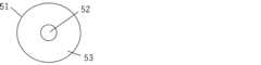
導電性部材として、ローラ形状を有する導電性部材(以降、「導電性ローラ」ともいう)を例に、図1を参照して説明する。図1は、導電性ローラの軸に沿う方向(以降、「長手方向」ともいう)に対して垂直な断面図である。導電性ローラ51は、円柱状の導電性の支持体52、支持体52の外周、すなわち支持体の外表面に形成された導電層53を有している。 The conductive member will be described with reference to FIG. 1, taking as an example a conductive member having a roller shape (hereinafter also referred to as "conductive roller"). FIG. 1 is a cross-sectional view perpendicular to the direction along the axis of the conductive roller (hereinafter also referred to as the "longitudinal direction"). The
<支持体>
支持体を構成する材料としては、電子写真用の導電性部材の分野で公知なものや、導電性部材として利用できる材料から適宜選択して用いることができる。一例として、アルミニウム、ステンレス、導電性を有する合成樹脂、鉄、銅合金などの金属又は合金が挙げられる。
さらに、これらに対して、酸化処理やクロム、ニッケルなどで鍍金処理を施してもよい。鍍金の種類としては電気鍍金、無電解鍍金のいずれも使用することができる。寸法安定性の観点から無電解鍍金が好ましい。ここで使用される無電解鍍金の種類としては、ニッケル鍍金、銅鍍金、金鍍金、その他各種合金鍍金を挙げることができる。
鍍金厚さは、0.05μm以上が好ましく、作業効率と防錆能力のバランスを考慮すると、鍍金厚さは0.10μm~30.00μmであることが好ましい。支持体の円柱状の形状は、中実の円柱状でも、中空の円柱状(円筒状)でもよい。また、支持体の外径は、3mm~10mmの範囲が好ましい。<Support>
The material constituting the support can be appropriately selected from materials known in the field of conductive members for electrophotography and materials that can be used as conductive members. Examples include metals or alloys such as aluminum, stainless steel, conductive synthetic resins, iron, and copper alloys.
Furthermore, these may be subjected to oxidation treatment or plating treatment with chromium, nickel, or the like. As for the type of plating, either electroplating or electroless plating can be used. Electroless plating is preferred from the viewpoint of dimensional stability. Examples of the types of electroless plating used here include nickel plating, copper plating, gold plating, and various other alloy platings.
The plating thickness is preferably 0.05 μm or more, and in consideration of the balance between work efficiency and rust prevention ability, the plating thickness is preferably 0.10 μm to 30.00 μm. The columnar shape of the support may be a solid column or a hollow column (cylindrical). Further, the outer diameter of the support is preferably in the range of 3 mm to 10 mm.
支持体と導電層の間に、中抵抗層又は絶縁層が存在すると、放電による電荷の消費後の電荷の供給を迅速にできなくなる場合がある。よって、導電層は、支持体に直接設けるか、又はプライマーなどの、薄膜かつ導電性の樹脂層からなる中間層のみを介して支持体の外周に導電層を設けることが好ましい。
プライマーとしては、導電層形成用のゴム材料及び支持体の材質等に応じて公知のものを選択して用いることができる。プライマーの材料としては、例えば熱硬化性樹脂や熱可塑性樹脂が挙げられ、具体的には、フェノール系の樹脂、ウレタン系の樹脂、アクリル系の樹脂、ポリエステル系の樹脂、ポリエーテル系の樹脂、エポキシ系の樹脂のような公知の材料を用いることができる。If a medium resistance layer or an insulating layer is present between the support and the conductive layer, it may not be possible to quickly supply charge after the charge is consumed by discharge. Therefore, it is preferable to provide the conductive layer directly on the support, or to provide the conductive layer on the outer periphery of the support through only an intermediate layer made of a thin conductive resin layer such as a primer.
As the primer, a known primer can be selected and used depending on the rubber material for forming the conductive layer, the material of the support, etc. Examples of materials for the primer include thermosetting resins and thermoplastic resins, specifically phenolic resins, urethane resins, acrylic resins, polyester resins, polyether resins, Known materials such as epoxy resin can be used.
<導電層>
導電層は、マトリックス及びマトリックス中に分散された複数のドメインを有する。そして、マトリックスは、第一のゴムを含有し、ドメインは第二のゴム及び電子導電剤を含有する。そして、マトリックス及びドメインは、下記構成要素(i)及び(ii)を充足する。
構成要素(i):マトリックスの体積抵抗率R1が1.00×10¹²Ω・cmよりも大きく、1.00×10¹⁷Ω・cm以下である。
構成要素(ii):マトリックスの体積抵抗率R1が、ドメインの体積抵抗率R2の1.0×10⁵倍以上である。<Conductive layer>
The conductive layer has a matrix and multiple domains distributed within the matrix. The matrix then contains a first rubber, and the domains contain a second rubber and an electronically conductive agent. The matrix and domain satisfy the following constituent elements (i) and (ii).
Component (i): The volume resistivity R1 of the matrix is greater than 1.00×10¹² Ω·cm and equal to or less than 1.00×10¹⁷ Ω·cm.
Component (ii): The volume resistivity R1 of the matrix is 1.0×10⁵ times or more the volume resistivity R2 of the domain.
<構成要素(i);マトリックスの体積抵抗率>
マトリックスの体積抵抗率R1を、1.00×10¹²Ω・cmよりも大きくすることで、電荷がドメインを迂回してマトリックス中を移動することを抑制できる。そして、1回の放電で蓄積された電荷の大半が消費されることを抑制できる。また、ドメインに蓄積された電荷が、マトリックスに漏洩することによって、あたかも導電層内を連通する導電経路が形成されている状態となることを防止できる。
体積抵抗率R1は、2.00×10¹²Ω・cm以上であることが好ましい。
また、R1の上限は、1.00×10¹⁷Ω・cm以下である。好ましくは、9.00×10¹⁶Ω・cm以下である。<Component (i); Volume resistivity of matrix>
By setting the volume resistivity R1 of the matrix to be larger than 1.00×10¹² Ω·cm, it is possible to suppress charges from moving in the matrix by bypassing the domains. In addition, consumption of most of the accumulated charge in one discharge can be suppressed. Furthermore, it is possible to prevent charges accumulated in the domains from leaking into the matrix, resulting in a situation where a conductive path communicating within the conductive layer is formed.
It is preferable that the volume resistivity R1 is 2.00×10¹² Ω·cm or more.
Further, the upper limit of R1 is 1.00×10¹⁷ Ω·cm or less. Preferably, it is 9.00×10¹⁶ Ω·cm or less.
電荷を導電層中のドメインを介して移動させ、微細放電を達成するためには、電荷が十分に蓄積された領域(ドメイン)が、電気的に絶縁性の領域(マトリックス)で分断されている構成が有効であると本発明者らは考えている。そして、マトリックスの体積抵抗率を上記したような高抵抗領域の範囲とすることで、各ドメインとの界面において十分な電荷を留めることができ、また、ドメインからの電荷漏洩を抑制できる。 In order to move charge through domains in the conductive layer and achieve microdischarge, regions with sufficient charge accumulation (domains) are separated by electrically insulating regions (matrix). The inventors believe that the configuration is effective. By setting the volume resistivity of the matrix within the high resistance region as described above, sufficient charge can be retained at the interface with each domain, and charge leakage from the domains can be suppressed.
また、放電が微細でかつ必要十分な放電量を達成するためには、電荷の移動経路が、ドメインを介在した経路に限定することが極めて有効である。ドメインからのマトリックスへの電荷の漏洩を抑制し、電荷の輸送経路を複数のドメインを介した経路に限定することにより、ドメインに存在する電荷の密度を向上させることができるため、各ドメインにおける電荷の充填量をより増大させることができる。
これにより、放電の起点である導電相としてのドメインの表面において、放電に関与できる電荷の総数を向上させることができ、結果、導電性部材の表面からの放電の出やすさを向上させることができると考えられる。Furthermore, in order to achieve a fine discharge and a necessary and sufficient amount of discharge, it is extremely effective to limit the charge movement path to a path that involves domains. By suppressing the leakage of charge from the domain to the matrix and limiting the charge transport route to a route that passes through multiple domains, the density of charge existing in the domain can be improved, so the charge in each domain can be increased. The amount of filling can be further increased.
This makes it possible to increase the total number of charges that can participate in discharge on the surface of the domain as a conductive phase, which is the starting point of discharge, and as a result, it is possible to improve the ease with which discharge comes out from the surface of the conductive member. It seems possible.
・マトリックスの体積抵抗率の測定方法;
マトリックスの体積抵抗率は、導電層を薄片化し、微小探針によって計測することができる。薄片化の手段としては、ミクロトームのような非常に薄いサンプルを作製できる手段を用いる。具体的な手順については後述する。・Measurement method of matrix volume resistivity;
The volume resistivity of the matrix can be measured by cutting the conductive layer into a thin section and using a microprobe. As a means of thinning, a means capable of producing very thin samples, such as a microtome, is used. The specific procedure will be described later.
<構成要素(ii);ドメインの体積抵抗率>
マトリックスの体積抵抗率R1は、ドメインの体積抵抗率R2の1.0×10⁵倍以上である。
これにより、マトリックスで目的としない電荷の移動を抑制しつつ、電荷の輸送経路を複数のドメインを介する経路に限定しやすくなる。
R1はR2の、1.0×10⁵倍~1.0×10²⁰倍であることがより好ましく、1.0×10⁶倍~1.0×10¹⁸倍であることがさらに好ましく、1.0×10¹¹倍~1.0×10¹⁶倍であることがさらにより好ましい。
そしてR2は1.00×101Ω・cm以上、1.00×10⁴Ω・cm以下であることが好ましく、1.00×101Ω・cm以上1.00×10²Ω・cm以下であることがより好ましい。<Component (ii); volume resistivity of domain>
The volume resistivity R1 of the matrix is 1.0×10⁵ times or more the volume resistivity R2 of the domain.
This makes it easier to limit the charge transport route to a route that passes through a plurality of domains while suppressing the movement of unintended charges in the matrix.
R1 is more preferably 1.0 × 10⁵ times to 1.0 × 10²⁰ times, even more preferably 1.0 × 10⁶ times to 1.0 × 10¹⁸ times, and 1. Even more preferably it is .0×1011 times to 1.0×10¹⁶ times.
And R2 is preferably 1.00×101 Ω・cm or more and 1.00×10⁴ Ω・cm or less, and 1.00×101 Ω・cm or more and 1.00×10² Ω・cm or less It is more preferable that
上記を満たすことで、導電層内における電荷の輸送パスをコントロールでき、微細放電をより達成しやすくなる。そのため、過度な放電を抑制でき、画像流れを抑制できる。
ドメインの体積抵抗率は、例えば、ドメインのゴム成分に対し、電子導電剤の種類や量を変更することによって、その導電性を所定の値にすることで調整する。By satisfying the above requirements, the transport path of charge within the conductive layer can be controlled, making it easier to achieve fine discharge. Therefore, excessive discharge can be suppressed and image deletion can be suppressed.
The volume resistivity of the domain is adjusted by adjusting the conductivity to a predetermined value by, for example, changing the type and amount of the electronic conductive agent in the rubber component of the domain.
ドメイン用のゴム材料としては、マトリックス用としてのゴム成分を含むゴム組成物を用いることができる。マトリックスドメイン構造を形成するためにマトリックスを形成するゴム材料との溶解度パラメータ(SP値)の差を一定の範囲にすることが好ましい。すなわち、第一のゴムのSP値と第二のゴムのSP値との差の絶対値が、好ましくは0.4(J/cm3)0.5以上5.0(J/cm3)0.5以下であり、より好ましくは0.4(J/cm3)0.5以上2.2(J/cm3)0.5以下である。
ドメインの体積抵抗率は、電子導電剤の種類、及びその添加量を適宜選択することによって調整することができる。ドメインの体積抵抗率を1.00×101Ωcm以上1.00×10⁴Ωcm以下に制御するために使用する電子導電剤としては、分散する量によって高抵抗から低抵抗まで体積抵抗率を大きく変化させることができる電子導電剤が好ましい。As the rubber material for the domain, a rubber composition containing a rubber component for the matrix can be used. In order to form a matrix domain structure, it is preferable that the difference in solubility parameter (SP value) between the rubber material and the rubber material forming the matrix is within a certain range. That is, the absolute value of the difference between the SP value of the first rubber and the SP value of the second rubber is preferably 0.4 (J/cm3 )0.5 or more and 5.0 (J/cm3 )0 .5 or less, more preferably 0.4 (J/cm3 )0.5 or more and 2.2 (J/cm3 )0.5 or less.
The volume resistivity of the domain can be adjusted by appropriately selecting the type of electron conductive agent and the amount added thereof. As an electronic conductive agent used to control the volume resistivity of the domain to 1.00×101 Ωcm or more and 1.00×10⁴ Ωcm or less, the volume resistivity can be increased from high resistance to low resistance depending on the amount dispersed. Electronically conductive agents that can be varied are preferred.
ドメインに配合される電子導電剤については、カーボンブラック、グラファイト、酸化チタン、酸化錫等の酸化物;Cu、Ag等の金属;酸化物又は金属が表面に被覆され導電化された粒子等を例として挙げられる。また、必要に応じて、これらの導電剤の2種類以上を適宜量配合して使用してもよい。
以上の様な電子導電剤のうち、ゴムとの親和性が大きく、電子導電剤間の距離の制御が容易な、導電性のカーボンブラックを使用することが好ましい。ドメインに配合されるカーボンブラックの種類については、特に限定されるものではない。具体的には、例えば、ガスファーネスブラック、オイルファーネスブラック、サーマルブラック、ランプブラック、アセチレンブラック、ケッチェンブラック等が挙げられる。Examples of electronic conductive agents to be added to the domain include oxides such as carbon black, graphite, titanium oxide, and tin oxide; metals such as Cu and Ag; and particles whose surfaces are coated with oxides or metals to make them conductive. It is mentioned as. Furthermore, if necessary, two or more of these conductive agents may be used in appropriate amounts.
Among the above electron conductive agents, it is preferable to use conductive carbon black, which has a high affinity with rubber and allows easy control of the distance between the electron conductive agents. The type of carbon black added to the domain is not particularly limited. Specific examples include gas furnace black, oil furnace black, thermal black, lamp black, acetylene black, Ketjen black, and the like.
中でも、高い導電性をドメインに付与し得る、DBP吸油量が40cm3/100g以上170cm3/100g以下である導電性カーボンブラックを好適に用いることができる。
導電性のカーボンブラック等の電子導電剤の含有量は、ドメインに含まれる第二のゴム100質量部に対して、20質量部以上150質量部以下が好ましい。より好ましくは、50質量部以上100質量部以下である。
一般的な電子写真用の導電性部材と比較して、導電剤が多量に配合されていることが好ましい。これにより、ドメインの体積抵抗率を1.00×101Ωcm以上1.00×10⁴Ω・cm以下の範囲に容易に制御することができる。
また、必要に応じて、ゴムの配合剤として一般に用いられている充填剤、加工助剤、架橋助剤、架橋促進剤、老化防止剤、架橋促進助剤、架橋遅延剤、軟化剤、分散剤、着色剤等を、本開示に係る効果を阻害しない範囲でドメイン用のゴム組成物に添加してもよい。Among them, conductive carbon black having a DBP oil absorption of 40 cm3 /100 g or more and 170 cm3 /100 g or less, which can impart high conductivity to the domains, can be suitably used.
The content of the electronic conductive agent such as conductive carbon black is preferably 20 parts by mass or more and 150 parts by mass or less with respect to 100 parts by mass of the second rubber included in the domain. More preferably, it is 50 parts by mass or more and 100 parts by mass or less.
It is preferable that a larger amount of a conductive agent is blended than in a general conductive member for electrophotography. Thereby, the volume resistivity of the domain can be easily controlled within the range of 1.00×101 Ωcm to 1.00×10⁴ Ω·cm.
In addition, fillers, processing aids, crosslinking aids, crosslinking accelerators, anti-aging agents, crosslinking accelerators, crosslinking retarders, softeners, and dispersants that are commonly used as compounding agents for rubber may also be used as necessary. , colorants, etc. may be added to the rubber composition for the domain within a range that does not impede the effects of the present disclosure.
・ドメインの体積抵抗率の測定方法;
ドメインの体積抵抗率の測定は、マトリックスの体積抵抗率の測定方法に対して、測定箇所をドメインに相当する場所に変更し、電流値の測定の際の印可電圧を1Vに変更した以外は同様の方法で実施すればよい。具体的な手順は後述する。・Method for measuring domain volume resistivity;
The measurement of the volume resistivity of the domain was the same as the method for measuring the volume resistivity of the matrix, except that the measurement location was changed to a location corresponding to the domain, and the applied voltage when measuring the current value was changed to 1V. This can be done using the following method. The specific procedure will be described later.
<構成要素(iii);ドメインの隣接壁面間距離>
ドメイン同士での電荷の授受を行わせるうえで、導電層の厚み方向の断面観察における、ドメインの隣接壁面間距離の算術平均値Dm(以降、単に「ドメイン間距離Dm」ともいう)は、好ましくは2.00μm以下であり、より好ましくは1.00μm以下である。
また、ドメイン同士を絶縁領域(マトリックス)で電気的に確実に分断し、電荷をドメインにより蓄積しやすくなることができるため、ドメイン間距離Dmは、好ましくは0.15μm以上であり、より好ましくは0.20μm以上である。<Component (iii); Distance between adjacent wall surfaces of domains>
In order to transfer charges between domains, the arithmetic mean value Dm of the distance between adjacent wall surfaces of domains (hereinafter also simply referred to as "interdomain distance Dm") in cross-sectional observation in the thickness direction of the conductive layer is preferably is 2.00 μm or less, more preferably 1.00 μm or less.
In addition, since domains can be reliably electrically separated by an insulating region (matrix) and charges can be easily accumulated in the domains, the inter-domain distance Dm is preferably 0.15 μm or more, and more preferably It is 0.20 μm or more.
・ドメイン間距離Dmの測定方法;
ドメイン間距離Dmの測定方法は、次のように実施すればよい。
まず、前述のマトリックスの体積抵抗率の測定における方法と同様の方法で切片を作製する。また、マトリックスドメイン構造の観察を好適に実施するために、染色処理、蒸着処理など、導電相と絶縁相とのコントラストが好適に得られる前処理を施してもよい。
破断面の形成、白金蒸着を行った切片を、走査型電子顕微鏡(SEM)によって観察して、マトリックスドメイン構造の存在を確認する。これらの中でも、ドメインの面積の定量化の正確性から、SEMで、5000倍で観察を行うことが好ましい。具体的な手順は後述する。・Measurement method of inter-domain distance Dm;
The inter-domain distance Dm may be measured as follows.
First, a section is prepared in the same manner as in the measurement of the volume resistivity of the matrix described above. Further, in order to suitably observe the matrix domain structure, a pretreatment such as a dyeing treatment or a vapor deposition treatment that can suitably obtain a contrast between the conductive phase and the insulating phase may be performed.
A section in which a fractured surface has been formed and platinum vapor deposited is observed using a scanning electron microscope (SEM) to confirm the presence of a matrix domain structure. Among these, from the viewpoint of accuracy in quantifying the area of the domain, it is preferable to perform observation using a SEM at a magnification of 5000 times. The specific procedure will be described later.
・ドメイン間距離Dmの均一性;
ドメイン間距離Dmの分布は均一であることが、より安定的に微細放電を形成できるため好ましい。ドメイン間距離Dmの分布が均一であることで、導電層内で局所的にドメイン間距離が長い箇所が一部できることで、電荷の供給が周囲比べて滞る箇所が生じた場合などに、放電の出やすさが抑制される現象を低減できる。
電荷が輸送される断面、すなわち、図3(b)に示されるような導電層の厚さ方向の断面において、導電層の外表面から支持体方向への深さ0.1T~0.9Tまでの厚み領域の任意の3か所における、50μm四方の観察領域を取得する。このとき、当該観察領域内のドメイン間距離Dm及びドメイン間距離の分布の標準偏差σmを用いて、ドメイン間距離の変動係数σm/Dmが0以上0.40以下であることが好ましく、0.10以上0.30以下であることがより好ましい。- Uniformity of inter-domain distance Dm;
It is preferable that the distribution of the inter-domain distance Dm be uniform because fine discharges can be formed more stably. The uniform distribution of the inter-domain distance Dm creates some areas in the conductive layer where the inter-domain distance is locally long, which can cause discharge to occur in areas where charge supply is delayed compared to the surrounding area. It is possible to reduce the phenomenon in which the ease of output is suppressed.
In the cross section where charges are transported, that is, the cross section in the thickness direction of the conductive layer as shown in FIG. Obtain observation areas of 50 μm square at three arbitrary locations in the thickness area. At this time, using the interdomain distance Dm and the standard deviation σm of the distribution of the interdomain distance in the observation area, it is preferable that the variation coefficient σm/Dm of the interdomain distance is 0 or more and 0.40 or less, and 0. More preferably, it is 10 or more and 0.30 or less.
・ドメイン間距離Dmの均一性の測定方法;
ドメイン間距離の均一性の測定は、ドメイン間距離の測定と同様に、破断面の直接観察で得られる画像を定量化することによって行うことができる。具体的な手順は後述する。・Method for measuring uniformity of inter-domain distance Dm;
Similar to the measurement of the interdomain distance, the uniformity of the interdomain distance can be measured by quantifying an image obtained by direct observation of the fracture surface. The specific procedure will be described later.
導電性部材は、例えば、下記工程(i)~(iv)を含む方法を経て形成することができる。
工程(i):カーボンブラック及び第二のゴムを含む、ドメイン形成用ゴム混合物(以降、「CMB」とも称する)を調製する工程;
工程(ii):第一のゴムを含むマトリックス形成用ゴム混合物(以降、「MRC」とも称する)を調製する工程;
工程(iii):CMBとMRCとを混練して、マトリックスドメイン構造を有するゴム混合物を調製する工程。
工程(iv):工程(iii)で調製したゴム混合物の層を、導電性支持体上に直接又は他の層を介して形成し、該ゴム組成物の層を硬化させて、導電層を形成する工程。The conductive member can be formed, for example, through a method including the following steps (i) to (iv).
Step (i): preparing a domain-forming rubber mixture (hereinafter also referred to as "CMB") comprising carbon black and a second rubber;
Step (ii): preparing a matrix-forming rubber mixture (hereinafter also referred to as "MRC") containing a first rubber;
Step (iii): A step of kneading CMB and MRC to prepare a rubber mixture having a matrix domain structure.
Step (iv): Forming a layer of the rubber mixture prepared in step (iii) on a conductive support directly or via another layer, and curing the layer of the rubber composition to form a conductive layer. The process of doing.
そして、構成要素(i)~(iii)は、例えば、上記各工程に用いる材料の選択、製造条件の調整により制御することができる。以下説明する。
まず、構成要素(i)に関して、マトリックスの体積抵抗率は、MRCの組成によって定まる。Components (i) to (iii) can be controlled, for example, by selecting materials used in each of the above steps and adjusting manufacturing conditions. This will be explained below.
First, regarding component (i), the volume resistivity of the matrix is determined by the composition of MRC.
MRCに用いる第一のゴムとしては、導電性の低いゴムが好ましい。天然ゴム、ブタジエンゴム、ブチルゴム、アクリロニトリルブタジエンゴム、ウレタンゴム、シリコーンゴム、フッ素ゴム、イソプレンゴム、クロロプレンゴム、スチレンブタジエンゴム、エチレンプロピレンゴム、エチレンプロピレンジエンゴム、及びポリノルボルネンゴムからなる群から選択される少なくとも一が好ましい。
第一のゴムが、ブチルゴム、スチレンブタジエンゴム、及びエチレンプロピレンジエンゴムからなる群から選択される少なくとも一がより好ましい。
また、マトリックスの体積抵抗率が上記範囲内であれば、MRCには、必要に応じて、充填剤、加工助剤、架橋剤、架橋助剤、架橋促進剤、架橋促進助剤、架橋遅延剤、老化防
止剤、軟化剤、分散剤、着色剤などを添加してもよい。一方、MRCには、マトリックスの体積抵抗率を上記範囲内とするために、カーボンブラックなどの電子導電剤は含有させないことが好ましい。As the first rubber used for MRC, a rubber with low conductivity is preferable. selected from the group consisting of natural rubber, butadiene rubber, butyl rubber, acrylonitrile butadiene rubber, urethane rubber, silicone rubber, fluororubber, isoprene rubber, chloroprene rubber, styrene butadiene rubber, ethylene propylene rubber, ethylene propylene diene rubber, and polynorbornene rubber. At least one of the above is preferred.
More preferably, the first rubber is at least one selected from the group consisting of butyl rubber, styrene butadiene rubber, and ethylene propylene diene rubber.
In addition, if the volume resistivity of the matrix is within the above range, MRC may include fillers, processing aids, crosslinking agents, crosslinking aids, crosslinking accelerators, crosslinking accelerators, crosslinking retarders, etc. , antiaging agents, softeners, dispersants, colorants, etc. may be added. On the other hand, in order to keep the volume resistivity of the matrix within the above range, it is preferable that the MRC does not contain an electronic conductive agent such as carbon black.
また、構成要素(ii)に関して、ドメインの体積抵抗率R2は、CMB中の電子導電剤の量によって調整し得る。例えば、電子導電剤として、DBP吸油量が、40cm3/100g以上170cm3/100g以下である導電性カーボンブラックを用いる場合を例に挙げる。CMBの第二のゴム100質量部に対し、40質量部以上200質量部以下の導電性カーボンブラックを含むようにCMBを調製することで所望の範囲を達成し得る。Also, regarding component (ii), the volume resistivity R2 of the domain can be adjusted by the amount of electronically conductive agent in the CMB. For example, a case is exemplified in which conductive carbon black having a DBP oil absorption of 40 cm3 /100 g or more and 170 cm3 /100 g or less is used as the electronic conductive agent. The desired range can be achieved by preparing the CMB so that it contains 40 parts by mass or more and 200 parts by mass or less of conductive carbon black with respect to 100 parts by mass of the second rubber of the CMB.
さらに、構成要素(iii)に関わるドメインの分散状態に関しては、下記(a)~(d)の4つを制御することが有効である。
(a)CMB、及びMRCの各々の界面張力σの差;
(b)CMBの粘度(ηd)、及びMRCの粘度(ηm)の比(ηm/ηd);
(c)工程(iii)における、CMBとMRCとの混練時のせん断速度(γ)、及びせん断時のエネルギー量(EDK)。
(d)工程(iii)における、CMBのMRCに対する体積分率。Furthermore, regarding the distributed state of domains related to component (iii), it is effective to control the following four points (a) to (d).
(a) Difference in interfacial tension σ between CMB and MRC;
(b) Ratio of CMB viscosity (ηd) and MRC viscosity (ηm) (ηm/ηd);
(c) Shear rate (γ) during kneading of CMB and MRC and energy amount during shearing (EDK) in step (iii).
(d) Volume fraction of CMB to MRC in step (iii).
(a)CMBとMRCとの界面張力差
一般的に二種の非相溶のゴムを混合した場合、相分離する。これは、異種高分子間の相互作用よりも、同一高分子間の相互作用が強いため、同一高分子同士で凝集し、自由エネルギーを低下させ安定化しようとするためである。
相分離構造の界面は異種高分子と接触するため、同一分子同士の相互作用で安定化されている内部より、自由エネルギーが高くなる。その結果、界面の自由エネルギーを低減させるために、異種高分子と接触する面積を小さくしようとする界面張力が発生する。この界面張力が小さい場合、エントロピーを増大させるために異種高分子でもより均一に混合しようとする方向に向かう。均一に混合した状態とは溶解であり、溶解度の目安となるSP値(溶解度パラメーター)と界面張力は相関する傾向にある。(a) Interfacial tension difference between CMB and MRC Generally, when two types of incompatible rubbers are mixed, phase separation occurs. This is because the interaction between the same polymers is stronger than the interaction between different types of polymers, so the same polymers aggregate with each other to lower their free energy and stabilize it.
Since the interface of a phase-separated structure comes into contact with different types of polymers, the free energy is higher than the interior, which is stabilized by interactions between the same molecules. As a result, in order to reduce the free energy of the interface, interfacial tension is generated that tends to reduce the area of contact with the different polymer. When this interfacial tension is small, even dissimilar polymers tend to be mixed more uniformly in order to increase entropy. A uniformly mixed state is a state of dissolution, and the SP value (solubility parameter), which is a measure of solubility, and interfacial tension tend to be correlated.
つまり、CMBとMRCとの界面張力差は、各々が含むゴムのSP値差と相関すると考えられる。MRC中の第一のゴムの溶解度パラメーターSP値と、CMB中の第二のゴムのSP値の絶対値の差が、好ましくは0.4(J/cm3)0.5以上5.0(J/cm3)0.5以下、より好ましくは0.4(J/cm3)0.5以上2.2(J/cm3)0.5以下となるようなゴムを選択することが好ましい。この範囲であれば安定した相分離構造を形成でき、また、CMBのドメイン径を小さくすることができる。In other words, the difference in interfacial tension between CMB and MRC is considered to be correlated with the difference in SP value of the rubbers each contains. The difference between the absolute value of the solubility parameter SP value of the first rubber in MRC and the SP value of the second rubber in CMB is preferably 0.4 (J/cm3 )0.5 or more and 5.0 ( It is preferable to select a rubber that has a value of J/cm3 )0.5 or less, more preferably 0.4 (J/cm3 )0.5 or more and 2.2 (J/cm3 )0.5 or less. . Within this range, a stable phase separation structure can be formed and the CMB domain diameter can be reduced.
ここで、CMBに用い得る第二のゴムの具体例としては、例えば、天然ゴム(NR)、イソプレンゴム(IR)、ブタジエンゴム(BR)、アクリロニトリルブタジエンゴム(NBR)、スチレンブタジエンゴム(SBR)、ブチルゴム(IIR)、エチレンプロピレンゴム(EPM)、エチレンプロピレンジエンゴム(EPDM)、クルルプレンゴム(CR)、ニトリルゴム(NBR)、水素添加ニトリルゴム(H-NBR)、シリコーンゴム、及びウレタンゴム(U)からなる群から選択される少なくとも一が好ましい。
第二のゴムが、ブタジエンゴム(BR)、スチレンブタジエンゴム(SBR)、ブチルゴム(IIR)、及びアクリロニトリルブタジエンゴム(NBR)からなる群から選択される少なくとも一がより好ましく、ブタジエンゴム(BR)、スチレンブタジエンゴム(SBR)、及びブチルゴム(IIR)からなる群から選択される少なくとも一がさらに好ましい。ブタジエンゴム(BR)及びブチルゴム(IIR)からなる群から選択される少なくとも一がさらにより好ましい。
導電層の厚みは、目的とする導電性部材の機能及び効果が得られるものであれば特に限
定されない。導電層の厚みは、1.0mm以上4.5mm以下とすることが好ましい。
ドメインとマトリクスとの質量比率(ドメイン:マトリクス)は、好ましくは5:95~40:60であり、より好ましくは10:90~30:70であり、さらに好ましくは13:87~25:75である。Here, specific examples of the second rubber that can be used for CMB include natural rubber (NR), isoprene rubber (IR), butadiene rubber (BR), acrylonitrile butadiene rubber (NBR), and styrene butadiene rubber (SBR). , butyl rubber (IIR), ethylene propylene rubber (EPM), ethylene propylene diene rubber (EPDM), Kururuprene rubber (CR), nitrile rubber (NBR), hydrogenated nitrile rubber (H-NBR), silicone rubber, and urethane rubber At least one selected from the group consisting of (U) is preferred.
More preferably, the second rubber is at least one selected from the group consisting of butadiene rubber (BR), styrene butadiene rubber (SBR), butyl rubber (IIR), and acrylonitrile butadiene rubber (NBR), and butadiene rubber (BR), At least one selected from the group consisting of styrene-butadiene rubber (SBR) and butyl rubber (IIR) is more preferred. Even more preferred is at least one selected from the group consisting of butadiene rubber (BR) and butyl rubber (IIR).
The thickness of the conductive layer is not particularly limited as long as the desired function and effect of the conductive member can be obtained. The thickness of the conductive layer is preferably 1.0 mm or more and 4.5 mm or less.
The mass ratio of domain and matrix (domain:matrix) is preferably 5:95 to 40:60, more preferably 10:90 to 30:70, and even more preferably 13:87 to 25:75. be.
<SP値の測定方法>
SP値は、SP値が既知の材料を用いて、検量線を作成することで、精度良く算出することが可能である。この既知のSP値は、材料メーカーのカタログ値を用いることもできる。例えば、NBR及びSBRは、分子量に依存せず、アクリロニトリル及びスチレンの含有比率でSP値がほぼ決定される。
従って、マトリックス及びドメインを構成するゴムを、熱分解ガスクロマトグラフィー(Py-GC)及び固体NMR等の分析手法を用いて、アクリロニトリル又はスチレンの含有比率を解析する。それにより、SP値が既知の材料から得た検量線から、SP値を算出することができる。
また、イソプレンゴムは、1,2-ポリイソプレン、1,3-ポリイソプレン、3,4-ポリイソプレン、及びcis-1,4-ポリイソプレン、trans-1,4-ポリイソプレンなどの、異性体構造でSP値が決定される。従って、SBR及びNBRと同様にPy-GC及び固体NMR等で異性体含有比率を解析し、SP値が既知の材料から、SP値を算出することができる。
SP値が既知の材料のSP値は、Hansen球法で求めたものである。<Measurement method of SP value>
The SP value can be calculated with high accuracy by creating a calibration curve using a material with a known SP value. For this known SP value, a material manufacturer's catalog value can also be used. For example, for NBR and SBR, the SP value is almost determined by the content ratio of acrylonitrile and styrene, without depending on the molecular weight.
Therefore, the content ratio of acrylonitrile or styrene in the rubber constituting the matrix and the domains is analyzed using analysis techniques such as pyrolysis gas chromatography (Py-GC) and solid-state NMR. Thereby, the SP value can be calculated from a calibration curve obtained from a material with a known SP value.
In addition, isoprene rubber includes isomers such as 1,2-polyisoprene, 1,3-polyisoprene, 3,4-polyisoprene, cis-1,4-polyisoprene, and trans-1,4-polyisoprene. The structure determines the SP value. Therefore, similarly to SBR and NBR, the isomer content ratio can be analyzed using Py-GC, solid-state NMR, etc., and the SP value can be calculated from a material whose SP value is known.
The SP value of a material whose SP value is known is determined by the Hansen sphere method.
(b)CMBとMRCとの粘度比
CMBとMRCとの粘度比(CMB/MRC)(ηd/ηm)は、1に近い程、ドメイン径を小さくできる。具体的には、粘度比は1.0以上2.0以下であることが好ましい。CMBとMRCの粘度比は、CMB及びMRCに使用する原料ゴムのムーニー粘度の選択や、充填剤の種類や量の配合によって調整が可能である。
また、相分離構造の形成を妨げない程度に、パラフィンオイルなどの可塑剤を添加することでも可能である。また混練時の温度を調整することで、粘度比の調整を行うことができる。
なおドメイン形成用ゴム混合物やマトリックス形成用ゴム混合物の粘度は、JIS K6300-1:2013に基づきムーニー粘度ML(1+4)を混練時のゴム温度で測定することで得られる。(b) Viscosity ratio between CMB and MRC The closer the viscosity ratio between CMB and MRC (CMB/MRC) (ηd/ηm) is to 1, the smaller the domain diameter can be. Specifically, the viscosity ratio is preferably 1.0 or more and 2.0 or less. The viscosity ratio of CMB and MRC can be adjusted by selecting the Mooney viscosity of the raw rubber used for CMB and MRC, and by blending the type and amount of filler.
It is also possible to add a plasticizer such as paraffin oil to an extent that does not hinder the formation of a phase-separated structure. Further, the viscosity ratio can be adjusted by adjusting the temperature during kneading.
The viscosity of the domain-forming rubber mixture and the matrix-forming rubber mixture can be obtained by measuring the Mooney viscosity ML(1+4) at the rubber temperature during kneading based on JIS K6300-1:2013.
(c)MRCとCMBとの混練時のせん断速度、及びせん断時のエネルギー量
MRCとCMBとの混練時のせん断速度は速いほど、また、せん断時のエネルギー量は大きいほど、ドメイン間距離Dmを小さくすることができる。
せん断速度は、混練機のブレードやスクリューといった撹拌部材の内径を大きくし、撹拌部材の端面から混練機内壁までの間隙を小さくすることや、回転数を大きくすることで上げることができる。またせん断時のエネルギーを上げるには、撹拌部材の回転数を上げることや、CMB中の第一のゴムとMRC中の第二のゴムの粘度を上げることで達成できる。(c) Shearing rate during kneading of MRC and CMB and energy amount during shearing The faster the shearing rate during kneading MRC and CMB, and the larger the amount of energy during shearing, the greater the interdomain distance Dm. Can be made smaller.
The shear rate can be increased by increasing the inner diameter of the stirring member such as the blade or screw of the kneading machine, by reducing the gap from the end face of the stirring member to the inner wall of the kneading machine, or by increasing the rotation speed. Moreover, increasing the energy during shearing can be achieved by increasing the rotational speed of the stirring member or by increasing the viscosity of the first rubber in the CMB and the second rubber in the MRC.
(d)MRCに対するCMBの体積分率
MRCに対するCMBの体積分率は、マトリックス形成用ゴム混合物に対するドメイン形成用ゴム混合物の衝突合体確率と相関する。具体的には、マトリックス形成用ゴム混合物に対するドメイン形成用ゴム混合物の体積分率を低減させると、ドメイン形成用ゴム混合物とマトリックス形成用ゴム混合物の衝突合体確率が低下する。つまり必要な導電性を得られる範囲において、マトリックス中におけるドメインの体積分率を減らすことでドメイン間距離Dmを小さくできる。
そして、CMBのMRCに対する体積分率(すなわち、ドメインのマトリクスに対する
体積分率)は、15%以上40%以下とすることが好ましい。(d) Volume fraction of CMB to MRC The volume fraction of CMB to MRC correlates with the collision coalescence probability of the domain-forming rubber mixture to the matrix-forming rubber mixture. Specifically, when the volume fraction of the domain-forming rubber mixture to the matrix-forming rubber mixture is reduced, the probability of collision and coalescence of the domain-forming rubber mixture and the matrix-forming rubber mixture decreases. In other words, the inter-domain distance Dm can be reduced by reducing the volume fraction of domains in the matrix within a range in which the required conductivity can be obtained.
The volume fraction of the CMB with respect to the MRC (that is, the volume fraction of the domain with respect to the matrix) is preferably 15% or more and 40% or less.
また、導電性部材における、導電層の長手方向の長さをLとし、導電層の厚さをTとしたとき、導電層の長手方向の中央、及び導電層の両端から中央に向かってL/4の3か所における、図3(b)に示されるような導電層の厚さ方向の断面を取得する。導電層の厚さ方向の断面の各々について、以下を満たすことが好ましい。
該各々の断面において、導電層の外表面から深さ0.1T~0.9Tまでの厚み領域の任意の3か所に15μm四方の観察領域を置いたときに、全9個の該観察領域の各々で観察されるドメインのうちの80個数%以上が、下記構成要素(iv)及び(v)を満たすことが好ましい。
構成要素(iv)
ドメインの断面積のうち該ドメインに含まれる電子導電剤の断面積の割合μrが、20%以上であること。
構成要素(v)
ドメインの周囲長をA、該ドメインの包絡周囲長をBとしたとき、A/Bが、1.00以上1.10以下であること。In addition, when the length of the conductive layer in the longitudinal direction of the conductive member is L, and the thickness of the conductive layer is T, L/ The cross sections in the thickness direction of the conductive layer as shown in FIG. 3(b) are obtained at three locations of No. 4. It is preferable that each cross section of the conductive layer in the thickness direction satisfies the following.
In each cross section, when observation areas of 15 μm square are placed at any three locations in the thickness region from the outer surface of the conductive layer to a depth of 0.1T to 0.9T, a total of nine observation areas It is preferable that 80% or more of the domains observed in each of these satisfy the following constituent elements (iv) and (v).
Component (iv)
The ratio μr of the cross-sectional area of the electron conductive agent included in the domain to the cross-sectional area of the domain is 20% or more.
Component (v)
When the perimeter of a domain is A and the envelope perimeter of the domain is B, A/B is 1.00 or more and 1.10 or less.
上記構成要素(iv)及び構成要素(v)は、ドメインの形状に係る規定ということができる。「ドメインの形状」とは、導電層の厚さ方向の断面に現れたドメインの断面形状として定義される。 The above component (iv) and component (v) can be said to be regulations regarding the shape of the domain. The "shape of a domain" is defined as the cross-sectional shape of a domain appearing in a cross section in the thickness direction of a conductive layer.
ドメインの形状は、その周面に凹凸がない形状、すなわち球体に近い形状であることが好ましい。形状に関する凹凸構造の数を低減することによって、ドメイン間の電界の不均一性を低減でき、つまり、電界集中が生じる箇所を少なくして、マトリックスで必要以上の電荷輸送が起きる現象を低減できる。
本発明者らは、1個のドメインに含まれる電子導電剤の量が、当該ドメインの外形形状に影響を与えているとの知見を得た。すなわち、1個のドメインの電子導電剤の充填量が増えるにつれて、該ドメインの外形形状がより球体に近くなるとの知見を得た。球体に近いドメインの数が多いほど、ドメイン間での電子の授受の集中点を少なくすることができる。The shape of the domain is preferably a shape without unevenness on its peripheral surface, that is, a shape close to a sphere. By reducing the number of concavo-convex structures in terms of shape, it is possible to reduce the non-uniformity of the electric field between domains, that is, it is possible to reduce the number of locations where electric field concentration occurs, and to reduce the phenomenon in which more than necessary charge transport occurs in the matrix.
The present inventors have found that the amount of electronic conductive agent contained in one domain influences the external shape of the domain. That is, it has been found that as the amount of electronic conductive agent filled in one domain increases, the external shape of the domain becomes closer to a sphere. The greater the number of domains that are close to a sphere, the fewer the concentration points of electron exchange between domains can be reduced.
そして、本発明者らの検討によれば、1つのドメインの断面の面積を基準として、当該断面において観察される電子導電剤の断面積の総和の割合μrが20%以上であるドメインは、より、球体に近い形状を取り得る。
その結果、ドメイン間での電子の授受の集中を有意に緩和し得る外形形状を取り得るため好ましい。具体的には、ドメインの断面積に対する該ドメインが含む該電子導電剤の断面積の割合μrが、20%以上であることが好ましい。より好ましくは、25%~30%である。
上記範囲にあることで、高速プロセス下においても、十分な電荷供給量を可能とすることができる。According to the studies of the present inventors, domains in which the ratio μr of the total cross-sectional area of the electron conductive agent observed in the cross-section is 20% or more, based on the area of the cross-section of one domain, are more , can take a shape close to a sphere.
As a result, it is possible to take an external shape that can significantly alleviate the concentration of electron exchange between domains, which is preferable. Specifically, it is preferable that the ratio μr of the cross-sectional area of the electron conductive agent included in the domain to the cross-sectional area of the domain is 20% or more. More preferably, it is 25% to 30%.
By being within the above range, a sufficient amount of charge can be supplied even under high-speed processes.
ドメインの周面の凹凸がない形状に関しては、下記式(5)を満たすことが好ましいことを本発明者らは見出した。
1.00≦A/B≦1.10 (5)
(A:ドメインの周囲長、B:ドメインの包絡周囲長)The present inventors have found that it is preferable to satisfy the following formula (5) with regard to the shape of the peripheral surface of the domain without unevenness.
1.00≦A/B≦1.10 (5)
(A: perimeter of domain, B: envelope perimeter of domain)
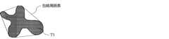
式(5)は、ドメインの周囲長Aと、ドメインの包絡周囲長Bとの比を示している。ここで、包絡周囲長とは、図6に示されるように、観察領域で観察されるドメイン71の凸部を結んだときの周囲長である。
ドメインの周囲長と、ドメインの包絡周囲長との比は1が最小値であり、1である状態
は、ドメインが真円又は楕円等の断面形状に凹部がない形状であることを示す。これらの比が1.1以下であると、ドメインに大きな凸凹形状が存在しないことを示し、電界の異方性が発現しにくい。Equation (5) indicates the ratio between the domain perimeter A and the domain envelope perimeter B. Here, the envelope perimeter is the perimeter when the convex portions of the
The minimum value of the ratio of the perimeter of the domain to the envelope perimeter of the domain is 1, and a state of 1 indicates that the domain has a cross-sectional shape such as a perfect circle or an ellipse without a recess. When these ratios are 1.1 or less, it means that there is no large uneven shape in the domain, and electric field anisotropy is less likely to occur.
<ドメインの形状に関する各パラメーターの測定方法>
導電性部材(導電性ローラ)の導電層から、ミクロトーム(商品名:Leica EM
FCS、ライカマイクロシステムズ社製)を用いて、切削温度-100℃にて、1μmの厚みの超薄切片を切り出す。ただし、下記のように、導電性部材の長手方向に対して垂直な断面によって、切片を作製し、当該切片の破断面におけるドメインの形状を評価する必要がある。この理由を下記に述べる。
図3(a)及び図3(b)に、導電性部材81を、3軸、具体的にはX、Y、Z軸の3次元としてその形状を示した図を示す。図3(a)及び図3(b)においてX軸は導電性部材の長手方向(軸方向)と平行な方向、Y軸、Z軸は導電性部材の軸方向と垂直な方向を示す。<Method for measuring each parameter related to domain shape>
From the conductive layer of the conductive member (conductive roller), a microtome (product name: Leica EM)
Ultra-thin sections with a thickness of 1 μm are cut using FCS (manufactured by Leica Microsystems) at a cutting temperature of -100°C. However, as described below, it is necessary to prepare a section using a cross section perpendicular to the longitudinal direction of the conductive member and evaluate the shape of the domain on the fracture surface of the section. The reason for this will be explained below.
FIGS. 3A and 3B are diagrams showing the shape of the
図3(a)は、導電性部材に対して、XZ平面82と平行な断面82aで導電性部材を切り出すイメージ図を示す。XZ平面は導電性部材の軸を中心として、360°回転することができる。導電性部材が感光体ドラムに対して当接されて回転し、感光ドラムとの隙間を通過する際に放電することを考慮すると、当該XZ平面82と平行な断面82aは、あるタイミングに同時に放電が起きる面を示していることになる。一定量の断面82aに相当する面が通過することによって、感光ドラムの表面電位が形成される。 FIG. 3A shows an image diagram of cutting out the conductive member at a
したがって、導電性部材内の電界集中と相関する、ドメインの形状の評価のためには、断面82aのようなある一瞬において同時に放電が発生する断面の解析ではなく、一定量の断面82aを含むドメイン形状の評価ができる導電性部材の軸方向と垂直なYZ平面83と平行な断面での評価が必要である。
この評価に、該導電層の長手方向の長さをLとしたとき、導電層の長手方向の中央での断面83bと、及び該導電層の両端から中央に向かってL/4の2か所の断面(83a及び83c)の計3か所を選択する。
また、当該断面83a~83cの観察位置に関しては、導電層の厚さをTとしたとき、各切片のそれぞれ外表面から深さ0.1T以上0.9T以下までの厚み領域の任意の3か所で15μm四方の観察領域を置いたときの、合計9か所の観察領域で測定を行えばよい。Therefore, in order to evaluate the shape of a domain, which is correlated with electric field concentration within a conductive member, it is necessary to analyze a domain that includes a certain amount of
For this evaluation, when the length in the longitudinal direction of the conductive layer is L, the cross section 83b at the center in the longitudinal direction of the conductive layer, and two points L/4 from both ends of the conductive layer toward the center. A total of three locations in the cross section (83a and 83c) are selected.
Regarding the observation positions of the
得られた切片に対し、白金を蒸着させ蒸着切片を得る。次いで当該蒸着切片の表面を、走査型電子顕微鏡(SEM)(商品名:S-4800、(株)日立ハイテクノロジーズ製)を用いて1000倍又は5000倍で撮影し、観察画像を得る。
次に、当該解析画像内のドメインの形状を定量化するために、画像処理ソフト(商品名:ImageProPlus;Media Cybernetics社製)を使用して、8ビットのグレースケール化を行い、256諧調のモノクロ画像を得る。次いで、破断面内のドメインが白くなるように、画像の白黒を反転処理し、2値化画像を得る。Platinum is deposited on the obtained section to obtain a vapor-deposited section. Next, the surface of the vapor-deposited section is photographed at 1000 times or 5000 times using a scanning electron microscope (SEM) (trade name: S-4800, manufactured by Hitachi High-Technologies Corporation) to obtain an observation image.
Next, in order to quantify the shape of the domain in the analysis image, image processing software (product name: ImageProPlus; manufactured by Media Cybernetics Inc.) was used to convert it to 8-bit grayscale, and convert it into a 256-tone monochrome image. Get the image. Next, the black and white of the image is inverted so that the domain within the fracture surface becomes white, and a binarized image is obtained.
<<ドメイン内の電子導電剤の断面積割合μrの測定方法>>
ドメイン内の電子導電剤の断面積割合の測定は、上記5000倍で撮影した観察画像の2値化画像を定量化することによって行なうことができる。
画像処理ソフト(商品名:ImageProPlus;Media Cybernetics社製)によって、8ビットのグレースケール化を行い、256諧調のモノクロ画像を得る。当該観察画像に対して、カーボンブラックの粒子を区別できるように2値化を実施し、2値化画像を得る。得られた画像に対しカウント機能を使用することによって、当該解析画像内のドメインの断面積S及び当該ドメイン内に含まれる電子導電剤としてのカ
ーボンブラック粒子の断面積の合計Scを算出する。
そして、ドメイン内の電子導電材の断面積割合として、上記9か所におけるSc/Sの算術平均値μrを算出する。
電子導電剤の断面積割合μrは、ドメインの体積抵抗率の均一性に影響する。断面積割合μrの測定と合わせて、ドメインの体積抵抗率の均一性は以下のように測定できる。
上記測定方法により、ドメインの体積抵抗率の均一性の指標として、μr及びμrの標準偏差σrから、σr/μrを算出する。<<Method for measuring cross-sectional area ratio μr of electron conductive agent in domain>>
The cross-sectional area ratio of the electron conductive agent within the domain can be measured by quantifying the binarized image of the observation image taken at 5000 times the above magnification.
Image processing software (trade name: ImageProPlus; manufactured by Media Cybernetics) performs 8-bit grayscale conversion to obtain a monochrome image with 256 tones. The observed image is binarized so that carbon black particles can be distinguished, and a binarized image is obtained. By using a count function on the obtained image, the total Sc of the cross-sectional area S of the domain in the analyzed image and the cross-sectional area of the carbon black particles as an electron conductive agent contained in the domain is calculated.
Then, the arithmetic mean value μr of Sc/S at the nine locations is calculated as the cross-sectional area ratio of the electronically conductive material within the domain.
The cross-sectional area ratio μr of the electron conductive agent affects the uniformity of the volume resistivity of the domain. Together with the measurement of the cross-sectional area ratio μr, the uniformity of the volume resistivity of the domain can be measured as follows.
According to the above measurement method, σr/μr is calculated from μr and the standard deviation σr of μr as an index of the uniformity of the volume resistivity of the domain.
<<ドメインの周囲長A、包絡周囲長Bの測定方法>>
画像処理ソフトのカウント機能によって、上記1000倍で撮影した観察画像の2値化画像内に存在するドメイン群に対して下記の項目を算出する。
・周囲長A(μm)
・包絡周囲長B(μm)
これらの値を以下の式(5)に代入し、9か所の評価画像の算術平均値を採用する。
1.00≦A/B≦1.10 (5)
(A:ドメインの周囲長、B:ドメインの包絡周囲長)<<Measurement method of domain perimeter A and envelope perimeter B>>
Using the counting function of the image processing software, the following items are calculated for the domain group present in the binarized image of the observed image taken at 1000 times the magnification.
・Perimeter length A (μm)
・Envelope perimeter B (μm)
These values are substituted into the following equation (5), and the arithmetic mean value of the nine evaluation images is adopted.
1.00≦A/B≦1.10 (5)
(A: perimeter of domain, B: envelope perimeter of domain)
<<ドメインの形状指数の測定方法>>
ドメインの形状指数は、μr(面積%)が20%以上であり、かつ、ドメインの周囲長比A/Bが上記式(5)を満たすドメイン群の、ドメイン総数に対する個数パーセントを算出すればよい。ドメインの形状指数が、80個数%~100個数%であることが好ましい。
上記2値化画像に対して、画像処理ソフト(商品名:ImageProPlus;Media Cybernetics社製)のカウント機能を用いて、ドメイン群の2値化画像内の個数を算出し、さらに、μr≧20及び上記式(5)を満たすドメインの個数パーセントを求めればよい。<<Method for measuring domain shape index>>
The shape index of a domain may be calculated by calculating the number percentage of a group of domains whose μr (area %) is 20% or more and whose perimeter length ratio A/B satisfies the above formula (5) with respect to the total number of domains. . It is preferable that the shape index of the domains is 80% by number to 100% by number.
For the above binarized image, use the counting function of image processing software (product name: ImageProPlus; manufactured by Media Cybernetics) to calculate the number of domain groups in the binarized image, and further calculate the number of domain groups in the binarized image. What is necessary is to find the number percentage of domains that satisfy the above formula (5).
構成要素(iv)で規定したように、ドメイン中に電子導電剤を高密度に充填することで、ドメインの外形形状を球体に近づけることができると共に、構成(v)に規定したように凹凸が小さいものとすることができる。
構成要素(iv)で規定したような、電子導電剤が高密度に充填されたドメインを得るために、電子導電剤は、DBP吸油量が40cm3/100g以上80cm3/100g以下であるカーボンブラックを有することが好ましい。
DBP吸油量(cm3/100g)とは、100gのカーボンブラックが吸着し得るジブチルフタレート(DBP)の体積であり、日本工業規格(JIS) K 6217-4:2017(ゴム用カーボンブラック-基本特性-第4部:オイル吸収量の求め方(圧縮試料を含む))に従って測定される。
一般に、カーボンブラックは、平均粒径10nm以上50nm以下の一次粒子がアグリゲートした房状の高次構造を有している。この房状の高次構造はストラクチャーと呼ばれ、その程度はDBP吸油量(cm3/100g)で定量化される。As specified in component (iv), by filling the domain with an electronically conductive agent at high density, the external shape of the domain can be made close to a sphere, and as specified in component (v), unevenness can be reduced. It can be made small.
In order to obtain domains densely filled with the electronic conductive agent as defined in component (iv), the electronic conductive agent is carbon black whose DBP oil absorption is 40 cm3 /100 g or more and 80 cm3 /100 g or less. It is preferable to have.
DBP oil absorption (cm3 /100g) is the volume of dibutyl phthalate (DBP) that can be adsorbed by 100g of carbon black. - Measured according to Part 4: How to determine oil absorption (including compressed samples).
Generally, carbon black has a tuft-like higher-order structure in which primary particles having an average particle diameter of 10 nm or more and 50 nm or less are aggregated. This tuft-like higher-order structure is called a structure, and its degree is quantified by DBP oil absorption (cm3 /100g).
DBP吸油量が上記範囲内にある導電性カーボンブラックは、ストラクチャー構造が未発達のため、カーボンブラックの凝集が少なく、ゴムへの分散性が良好である。そのため、ドメイン中への充填量を多くでき、その結果として、外形形状が、より球体に近いドメインを得られやすい。
また、DBP吸油量が、上記した範囲内にある導電性カーボンブラックは、凝集体を形成し難いため、要件(v)に係るドメインを形成しやすくなる。Conductive carbon black having a DBP oil absorption within the above range has an undeveloped structure, so the carbon black has little agglomeration and has good dispersibility in rubber. Therefore, the amount of filling into the domain can be increased, and as a result, it is easy to obtain a domain whose external shape is closer to a sphere.
Further, conductive carbon black whose DBP oil absorption is within the above range is difficult to form aggregates, and therefore tends to form domains according to requirement (v).
<ドメイン径D>
導電層の断面から観察されるドメインの円相当径D(以降、単に「ドメイン径D」とも
いう)の算術平均値は、0.10μm以上5.00μm以下であることが好ましい。
この範囲であれば、最表面のドメインがトナーと同様以下のサイズとなるため、細かい放電が可能となり、均一放電を達成することが容易となる。
ドメイン径Dの平均値を、0.10μm以上とすることで、導電層において、電荷の移動する経路を目的とする経路により効果的に限定することができる。より好ましくは0.15μm以上であり、さらに好ましくは0.20μm以上である。
また、ドメイン径Dの平均値を5.00μm以下にすることで、ドメインの全体積に対する表面積の割合、すなわち、ドメインの比表面積を指数関数的に大きくすることができ、ドメインからの電荷の放出効率を飛躍的に向上させ得る。ドメイン径Dの平均値は、上記の理由から、2.00μm以下がより好ましく、1.00μm以下がさらに好ましい。
ドメイン径Dの平均値を、2.00μm以下にすることで、ドメインそのものの電気抵抗を低減できるため、単発の放電の量を必要十分量として、より効率的に微細放電が可能となる。<Domain diameter D>
The arithmetic mean value of the equivalent circle diameter D of the domains (hereinafter also simply referred to as "domain diameter D") observed from the cross section of the conductive layer is preferably 0.10 μm or more and 5.00 μm or less.
In this range, the outermost domain has a size similar to or smaller than that of the toner, so fine discharge becomes possible and uniform discharge is easily achieved.
By setting the average value of the domain diameter D to 0.10 μm or more, in the conductive layer, the path through which the charges move can be more effectively limited to the intended path. More preferably, it is 0.15 μm or more, and still more preferably 0.20 μm or more.
In addition, by setting the average value of the domain diameter D to 5.00 μm or less, the ratio of the surface area to the total area of the domain, that is, the specific surface area of the domain can be increased exponentially, and the release of charges from the domain Efficiency can be dramatically improved. For the above reasons, the average value of the domain diameter D is more preferably 2.00 μm or less, and even more preferably 1.00 μm or less.
By setting the average value of the domain diameter D to 2.00 μm or less, the electrical resistance of the domains themselves can be reduced, so that the amount of single discharge can be set to a necessary and sufficient amount, and fine discharge can be performed more efficiently.
なお、ドメイン間での電界集中のより一層の軽減を図る上では、ドメインの外形形状をより球体に近づけることが好ましい。そのためには、ドメイン径を、前記した範囲内でより小さくすることが好ましい。その方法としては、例えば、工程(iv)において、MRCとCMBとを混練して、MRCとCMBとを相分離させる。そして、MRCのマトリックス中にCMBのドメインを形成されたゴム混合物を調製する工程において、CMBのドメイン径を小さくするように制御する方法が挙げられる。
CMBのドメイン径を小さくすることでCMBの比表面積が増大し、マトリックスとの界面が増加するため、CMBのドメインの界面には張力を小さくしようとする張力が作用する。その結果、CMBのドメインは、その外形形状が、より球体に近づく。Note that in order to further reduce electric field concentration between domains, it is preferable to make the outer shape of the domains closer to a sphere. For this purpose, it is preferable to make the domain diameter smaller within the above range. As for this method, for example, in step (iv), MRC and CMB are kneaded to phase-separate the MRC and CMB. In the step of preparing a rubber mixture in which CMB domains are formed in an MRC matrix, there is a method in which the CMB domain diameter is controlled to be small.
By reducing the domain diameter of the CMB, the specific surface area of the CMB increases and the interface with the matrix increases, so a tension force that tries to reduce the tension acts on the interface of the CMB domains. As a result, the CMB domain has an outer shape closer to a sphere.
ここで、非相溶のポリマー2種を溶融混練させたときに形成されるマトリックス-ドメイン構造におけるドメイン径を決定する要素に関して、Taylorの式(式(6))、Wuの経験式(式(7)、(8))、及びTokitaの式(式(9))が知られている。
・Taylorの式
D=[C・σ/ηm・γ]・f(ηm/ηd) (6)
・Wuの経験式
γ・D・ηm/σ=4(ηd/ηm)0.84・ηd/ηm>1 (7)
γ・D・ηm/σ=4(ηd/ηm)-0.84・ηd/ηm<1 (8)
・Tokitaの式
D=12・P・σ・φ/(π・η・γ)・(1+4・P・φ・EDK/(π・η・γ))
(9)Here, regarding the factors that determine the domain diameter in the matrix-domain structure formed when two types of incompatible polymers are melt-kneaded, Taylor's formula (formula (6)), Wu's empirical formula (formula ( 7), (8)), and Tokita's formula (formula (9)) are known.
・Taylor's formula D=[C・σ/ηm・γ]・f(ηm/ηd) (6)
・Wu's empirical formula γ・D・ηm/σ=4(ηd/ηm)0.84・ηd/ηm>1 (7)
γ・D・ηm/σ=4(ηd/ηm)−0.84・ηd/ηm<1 (8)
・Tokita's formula D=12・P・σ・φ/(π・η・γ)・(1+4・P・φ・EDK/(π・η・γ))
(9)
式(6)~(9)において、Dは、CMBのドメインの最大フェレ径、Cは、定数、σは、界面張力、ηmは、マトリックスの粘度、ηdは、ドメインの粘度、γは、せん断速度、ηは、混合系の粘度、Pは、衝突合体確率、φは、ドメイン相体積、EDKは、ドメイン相切断エネルギーを表す。
構成要素(iii)に関連して、ドメイン間距離の均一化を図るためには、式(6)~(9)に従って、ドメイン径を小さくすることが有効である。さらに、MRCとCMBとを混錬する工程において、ドメインの原料ゴムが分裂し、徐々にその粒径が小さくなっていく過程において、混錬工程をどこで止めたかによってもドメイン間距離は変化する。
したがって、そのドメイン間距離の均一性は、混錬工程における混錬時間及びその混錬の強度の指数となる混錬回転数によって制御可能であり、混錬時間が長いほど、混錬回転数が大きいほどドメイン間距離の均一性を向上させることができる。In equations (6) to (9), D is the maximum Feret diameter of the CMB domain, C is a constant, σ is the interfacial tension, ηm is the viscosity of the matrix, ηd is the viscosity of the domain, and γ is the shear The velocity, η, is the viscosity of the mixed system, P is the collision coalescence probability, φ is the domain phase volume, and EDK is the domain phase cutting energy.
Regarding component (iii), in order to equalize the distance between domains, it is effective to reduce the domain diameter according to equations (6) to (9). Furthermore, in the process of kneading MRC and CMB, the distance between domains changes depending on where the kneading process is stopped in the process in which the raw rubber of the domains is split and its particle size gradually becomes smaller.
Therefore, the uniformity of the distance between domains can be controlled by the kneading time in the kneading process and the kneading rotation speed, which is an index of the kneading intensity.The longer the kneading time, the higher the kneading rotation speed. The larger the distance, the more uniform the inter-domain distances can be.
・ドメイン径Dの均一性;
ドメイン径Dは均一であること、つまり、粒度分布が狭い方が好ましい。導電層内の電荷が通るドメイン径Dの分布を均一とすることで、マトリックスドメイン構造内での電荷の集中を抑制し、導電性部材の全面にわたって放電の出やすさを効果的に増大することができる。
電荷が輸送される断面、すなわち、図3(b)に示されるような導電層の厚さ方向の断面において、導電層の外表面から支持体方向への深さ0.1T~0.9Tまでの厚み領域の任意の3か所における、50μm四方の観察領域を取得した際に、ドメイン径の標準偏差σd及びドメイン径の算術平均値Dの比σd/D(変動係数σd/D)が0以上0.40以下であることが好ましく、0.10以上0.30以下であることがより好ましい。- Uniformity of domain diameter D;
It is preferable that the domain diameter D is uniform, that is, the particle size distribution is narrow. By making uniform the distribution of the domain diameter D through which charges pass within the conductive layer, concentration of charges within the matrix domain structure is suppressed, and the ease with which discharge occurs over the entire surface of the conductive member is effectively increased. Can be done.
In the cross section where charges are transported, that is, the cross section in the thickness direction of the conductive layer as shown in FIG. When an observation area of 50 μm square is acquired at any three locations in the thickness region of It is preferably not less than 0.40, and more preferably not less than 0.10 and not more than 0.30.
ドメイン径の均一性を向上させるためには、前述のドメイン間距離の均一性を向上させる手法と等しく、式(6)~(9)に従い、ドメイン径を小さくすればドメイン径の均一性も向上する。さらにMRCとCMBとを混錬する工程において、ドメインの原料ゴムが分裂し、徐々にその粒径が小さくなっていく過程において、混錬工程をどこで止めたかによってもドメイン径の均一性は変化する。
したがって、そのドメイン径の均一性は、混錬工程における混錬時間及びその混錬の強度の指数となる混錬回転数によって制御可能であり、混錬時間が長いほど、混錬回転数が大きいほどドメイン径の均一性を向上させることができる。In order to improve the uniformity of the domain diameter, the same method as improving the uniformity of the distance between domains mentioned above, according to equations (6) to (9), if the domain diameter is made smaller, the uniformity of the domain diameter will also be improved. do. Furthermore, in the process of kneading MRC and CMB, the raw rubber of the domains splits and the particle size gradually decreases, and the uniformity of the domain diameter changes depending on where the kneading process is stopped. .
Therefore, the uniformity of the domain diameter can be controlled by the kneading time in the kneading process and the kneading rotation speed, which is an index of the kneading intensity; the longer the kneading time, the higher the kneading rotation speed. The more the uniformity of domain diameter can be improved.
・ドメイン径の均一性の測定方法;
ドメイン径の均一性の測定は、先に説明したドメイン間距離の均一性の測定と同様の方法で得られる、破断面の直接観察で得られる画像を定量化することによって行うことができる。具体的な手段は後述する。・Method for measuring uniformity of domain diameter;
The uniformity of the domain diameter can be measured by quantifying an image obtained by direct observation of the fracture surface, which is obtained by the same method as the measurement of the uniformity of the interdomain distance described above. Specific means will be described later.
<マトリックスドメイン構造の確認方法>
導電層中のマトリックスドメイン構造の存在は、導電層から薄片を作製して、薄片に形成した破断面の詳細観察により確認することができる。具体的な手順は後述する。<How to confirm matrix domain structure>
The presence of a matrix domain structure in the conductive layer can be confirmed by preparing a thin piece from the conductive layer and closely observing the fractured surface of the thin piece. The specific procedure will be described later.
<トナー>
以下、トナーについて説明する。
トナーは、結着樹脂を含有するトナー粒子、及び外添剤を有し、
該外添剤はハイドロタルサイト類化合物の微粒子を含有する。<Toner>
The toner will be explained below.
The toner has toner particles containing a binder resin and an external additive,
The external additive contains fine particles of a hydrotalcite compound.
ハイドロタルサイト類化合物の微粒子の一次粒子の個数平均粒径をLh(μm)としたとき、Lhが、0.10μm以上1.00μm以下であることが好ましい。上記範囲にあることで、ハイドロタルサイト類化合物の微粒子がドメインに安定して固着し、長期にわたって窒素酸化物(NOX)を吸着することができる。
また、Lhが0.10μm以上であることで、ハイドロタルサイト類化合物の微粒子が凝集体を形成しにくく、良好に窒素酸化物(NOX)を吸収できる。
Lhが1.00μm以下であることで、ハイドロタルサイト類化合物の微粒子のトナーからの移行が適切に起こり、帯電部材や感光体などの部材汚染を抑制できる。さらに比表面積が適度に大きくなるため、窒素酸化物(NOX)の吸収能力が向上する。Lhは、より好ましくは、0.15μm以上0.75μm以下である。When Lh (μm) is the number average particle size of the primary particles of fine particles of the hydrotalcite compound, it is preferable that Lh is 0.10 μm or more and 1.00 μm or less. By being within the above range, the fine particles of the hydrotalcite compound can stably adhere to the domain and adsorb nitrogen oxides (NOx ) over a long period of time.
Furthermore, when Lh is 0.10 μm or more, the fine particles of the hydrotalcite compound are less likely to form aggregates, and nitrogen oxides (NOx ) can be well absorbed.
When Lh is 1.00 μm or less, fine particles of the hydrotalcite compound can be appropriately transferred from the toner, and contamination of members such as a charging member and a photoreceptor can be suppressed. Furthermore, since the specific surface area becomes appropriately large, the ability to absorb nitrogen oxides (NOx ) is improved. Lh is more preferably 0.15 μm or more and 0.75 μm or less.
導電層の外表面から観察されるドメイン、すなわち、導電性部材の外表面に露出しているドメインの円相当径をLd(μm)としたとき、Ldは、0.10μm以上2.00μm以下であることが好ましく、0.15μm以上1.00μm以下であることがより好ましく、0.20μm以上0.70μm以下であることがさらに好ましい。
ドメイン径Ld(μm)は、ハイドロタルサイト類化合物の微粒子の一次粒子の個数平均粒径Lh(μm)以上であることが好ましい。ドメイン径Ld(μm)は、Lh(μm
)よりも大きいことがより好ましい。上記条件によってハイドロタルサイト類化合物の微粒子がより安定してドメインに固着する。より好ましくはLd/Lhが、1.10~4.00である。When the equivalent circle diameter of the domain observed from the outer surface of the conductive layer, that is, the domain exposed on the outer surface of the conductive member is Ld (μm), Ld is 0.10 μm or more and 2.00 μm or less. It is preferably 0.15 μm or more and 1.00 μm or less, and even more preferably 0.20 μm or more and 0.70 μm or less.
The domain diameter Ld (μm) is preferably equal to or larger than the number average particle diameter Lh (μm) of the primary particles of the hydrotalcite compound fine particles. The domain diameter Ld (μm) is Lh (μm
) is more preferable. Under the above conditions, the fine particles of the hydrotalcite compound are more stably fixed to the domain. More preferably, Ld/Lh is 1.10 to 4.00.
<ハイドロタルサイト類化合物の微粒子>
次に、ハイドロタルサイト類化合物の微粒子について説明する。
ハイドロタルサイト類化合物は、好ましくは下記式(A)で表すことができる。正極性に帯電した基本層(式(A)中の[M2+1-xM3+x(OH)-2])とネガ性に帯電した中間層(式(A)中の[x/nAn-・mH2O)とを有する層状の無機化合物である。
[M2+1-xM3+x(OH)-2][x/nAn-・mH2O] (A)
式(A)中、
M2+は、Mg2+,Zn2+などの2価金属イオンを表し、
M3+は、Al3+,Fe3+などの3価金属イオンを表し、
An-は、CO32-,Cl-,NO3-などのn価アニオンを表し、
m≧0である。<Fine particles of hydrotalcite compound>
Next, fine particles of hydrotalcite compounds will be explained.
The hydrotalcite compound can preferably be represented by the following formula (A). A positively charged basic layer ([M2+1−x M3+x(OH)−2 ] in formula (A)) and a negatively charged intermediate layer ([x/nAn−・ in formula (A)] mH2 O).
[M2+1-x M3+x (OH)-2 ] [x/nAn-・mH2 O] (A)
In formula (A),
M2+ represents a divalent metal ion such as Mg2+ or Zn2+ ,
M3+ represents a trivalent metal ion such as Al3+ or Fe3+ ;
An- represents an n-valent anion such as CO32- , Cl- , NO3- ,
m≧0.
式(A)に含まれる化合物の例としては、
[Mg2+0.750Al3+0.250(OH)-2.000][0.125CO32-・0.500H2O]が挙げられる。Examples of compounds included in formula (A) are:
Examples include [Mg2+0.750 Al3+0.250 (OH)−2.000 ] [0.125CO32−・0.500H2 O].
このように、ハイドロタルサイト類化合物は、その構造に由来して、粒子表面は正極性に帯電しているためドメインに固着しやすく、また、窒素酸化物を層の間に吸着しやすいと考えられる。そのため、高温高湿環境において感光体上で窒素酸化物と環境中の水分との接触を防ぎ、画像流れを抑えられると考えられる。
電荷の付与能力の観点から、式(A)において、2価の金属イオンM2+としてはMg2+が、3価の金属イオンM3+としてはAl3+が好ましい。また、n価アニオンとしては、トナー粒子への帯電性付与の観点から、CO32-,Cl-が好ましい。In this way, hydrotalcite compounds are thought to have a positively charged particle surface due to their structure, which makes them more likely to stick to domains, and to adsorb nitrogen oxides between the layers. It will be done. Therefore, it is thought that contact between nitrogen oxides and moisture in the environment on the photoreceptor can be prevented in a high-temperature, high-humidity environment, and image deletion can be suppressed.
From the viewpoint of charge imparting ability, in formula (A), Mg2+ is preferable as the divalent metal ion M2+ and Al3+ is preferable as the trivalent metal ion M3+ . Further, as the n-valent anion, CO32- and Cl- are preferable from the viewpoint of imparting chargeability to toner particles.
ハイドロタルサイト類化合物の微粒子の含有量は、トナー粒子100質量部に対して、0.01質量部~3.00質量部であることが好ましい。上記範囲であれば画像流れの抑制効果が得られやすい。より好ましくは0.10質量部~1.00質量部である。 The content of the fine particles of the hydrotalcite compound is preferably 0.01 parts by mass to 3.00 parts by mass based on 100 parts by mass of the toner particles. Within the above range, the effect of suppressing image deletion is likely to be obtained. More preferably, it is 0.10 parts by mass to 1.00 parts by mass.
ハイドロタルサイト類化合物の微粒子のトナー粒子に対する固着率は、20%以上60%以下であることがより好ましい。固着率がこの範囲内にあることで、ハイドロタルサイト類化合物の微粒子がトナー上に残り安定して帯電性を向上させつつ、帯電部材へも移行し、画像流れ抑制の効果がより顕著となる。より好ましい範囲は、40%以上60%以下である。
ハイドロタルサイト類化合物の微粒子のトナー粒子に対する固着率は、ハイドロタルサイト類化合物の微粒子の添加量、粒径、外添条件、トナー粒子の性状を調整することで制御することができる。The adhesion rate of the fine particles of the hydrotalcite compound to the toner particles is more preferably 20% or more and 60% or less. When the adhesion rate is within this range, the fine particles of the hydrotalcite compound remain stably on the toner and improve charging properties, while also transferring to the charging member, making the effect of suppressing image blurring more pronounced. . A more preferable range is 40% or more and 60% or less.
The adhesion rate of the fine particles of the hydrotalcite compound to the toner particles can be controlled by adjusting the amount of the fine particles of the hydrotalcite compound added, the particle size, the external addition conditions, and the properties of the toner particles.
また、トナー粒子には、ハイドロタルサイト類化合物の微粒子に加え、他の外添剤が添加されていてもよい。例えば、チタン酸塩の微粒子や、帯電性向上や流動性付与の観点からシリカ微粒子などが挙げられる。シリカ微粒子は、表面を疎水化処理した処理シリカ微粒子であることがより好ましい。
処理シリカ微粒子は、メタノール滴定試験によって測定された疎水化度が30体積%~80体積%であるものが好ましい。シリカ微粒子の含有量は、トナー粒子100質量部に対して、0.10質量部~4.50質量部であることが好ましく、より好ましくは0.10質量部~3.00質量部である。Further, in addition to the fine particles of the hydrotalcite compound, other external additives may be added to the toner particles. Examples include fine particles of titanate and fine silica particles from the viewpoint of improving chargeability and imparting fluidity. The silica fine particles are more preferably treated silica fine particles whose surfaces have been subjected to hydrophobization treatment.
The treated silica fine particles preferably have a degree of hydrophobicity of 30% to 80% by volume as measured by a methanol titration test. The content of the silica fine particles is preferably 0.10 parts by mass to 4.50 parts by mass, more preferably 0.10 parts by mass to 3.00 parts by mass, based on 100 parts by mass of toner particles.
<トナー粒子の製造方法>
トナー粒子の製造方法について説明する。
トナー粒子の製造方法は公知の手段を用いることができ、混練粉砕法や湿式製造法を用いることができる。粒子径の均一化や形状制御性の観点からは湿式製造法を好ましく用いることができる。さらに湿式製造法には懸濁重合法、溶解懸濁法、乳化重合凝集法、乳化凝集法などを挙げることができ、乳化凝集法を好ましく用いることができる。<Method for manufacturing toner particles>
A method for producing toner particles will be explained.
Known means can be used for manufacturing the toner particles, and a kneading and pulverizing method or a wet manufacturing method can be used. From the viewpoint of uniform particle diameter and shape controllability, a wet manufacturing method can be preferably used. Furthermore, wet manufacturing methods include a suspension polymerization method, a dissolution suspension method, an emulsion polymerization aggregation method, an emulsion aggregation method, and the like, and the emulsion aggregation method can be preferably used.
乳化凝集法では、まず、結着樹脂の微粒子や着色剤の微粒子などの材料を、分散安定剤を含有する水系媒体中で分散混合する。水系媒体中には、界面活性剤が添加されていてもよい。その後、凝集剤を添加することによって所望のトナー粒子の粒径となるまで凝集させ、その後又は凝集と同時に、樹脂微粒子間の融着を行う。さらに必要に応じて、熱による形状制御を行うことにより、トナー粒子を形成する。
ここで、結着樹脂の微粒子は、組成の異なる樹脂よりなる2層以上の構成とする複数層で形成された複合粒子とすることもできる。例えば、乳化重合法、ミニエマルション重合法、転相乳化法などにより製造、又はいくつかの製法を組み合わせて製造することができる。In the emulsion aggregation method, first, materials such as fine particles of a binder resin and fine particles of a colorant are dispersed and mixed in an aqueous medium containing a dispersion stabilizer. A surfactant may be added to the aqueous medium. Thereafter, an aggregating agent is added to agglomerate the toner particles until they reach a desired particle size, and then or simultaneously with the aggregation, the fine resin particles are fused together. Further, if necessary, toner particles are formed by performing shape control using heat.
Here, the fine particles of the binder resin may also be composite particles formed of a plurality of layers having two or more layers of resins having different compositions. For example, it can be produced by an emulsion polymerization method, a mini-emulsion polymerization method, a phase inversion emulsification method, or a combination of several production methods.
トナー粒子中に着色剤などの内添剤を含有させる場合は、樹脂微粒子に内添剤を含有させたものとしてもよく、また、別途内添剤のみからなる内添剤微粒子の分散液を調製し、該内添剤微粒子を、樹脂微粒子を凝集させる際に共に凝集させてもよい。
また、凝集時に組成の異なる樹脂微粒子を時間差で添加して凝集させることにより組成の異なる層構成のトナー粒子を作ることもできる。When toner particles contain an internal additive such as a colorant, the internal additive may be contained in resin fine particles, or a dispersion of internal additive fine particles consisting only of the internal additive may be separately prepared. However, the internal additive fine particles may be aggregated together when the resin fine particles are aggregated.
Furthermore, toner particles having layer structures having different compositions can also be produced by adding resin fine particles having different compositions at different times during aggregation and aggregating them.
分散安定剤としては以下のものを使用することができる。
無機分散安定剤として、リン酸三カルシウム、リン酸マグネシウム、リン酸亜鉛、リン酸アルミニウム、炭酸カルシウム、炭酸マグネシウム、水酸化カルシウム、水酸化マグネシウム、水酸化アルミニウム、メタ珪酸カルシウム、硫酸カルシウム、硫酸バリウム、ベントナイト、シリカ、アルミナが挙げられる。
また、有機系分散安定剤としては、ポリビニルアルコール、ゼラチン、メチルセルロース、メチルヒドロキシプロピルセルロース、エチルセルロース、カルボキシメチルセルロースのナトリウム塩、デンプンが挙げられる。As the dispersion stabilizer, the following can be used.
As an inorganic dispersion stabilizer, tricalcium phosphate, magnesium phosphate, zinc phosphate, aluminum phosphate, calcium carbonate, magnesium carbonate, calcium hydroxide, magnesium hydroxide, aluminum hydroxide, calcium metasilicate, calcium sulfate, barium sulfate , bentonite, silica, and alumina.
Further, examples of the organic dispersion stabilizer include polyvinyl alcohol, gelatin, methylcellulose, methylhydroxypropylcellulose, ethylcellulose, sodium salt of carboxymethylcellulose, and starch.
界面活性剤として、公知のカチオン性界面活性剤、アニオン性界面活性剤、ノニオン性界面活性剤を使用することができる。
カチオン性界面活性剤の具体例としては、ドデシルアンモニウムブロマイド、ドデシルトリメチルアンモニウムブロマイド、ドデシルピリジニウムクロライド、ドデシルピリジニウムブロマイド、ヘキサデシルトリメチルアンモニウムブロマイドなどが挙げられる。
ノニオン性界面活性剤の具体例としては、ドデシルポリオキシエチレンエーテル、ヘキサデシルポリオキシエチレンエーテル、ノニルフェニルポリキオシエチレンエーテル、ラウリルポリオキシエチレンエーテル、ソルビタンモノオレアートポリオキシエチレンエーテル、スチリルフェニルポリオキシエチレンエーテル、モノデカノイルショ糖などが挙げられる。
アニオン性界面活性剤の具体例としては、ステアリン酸ナトリウム、ラウリン酸ナトリウムなどの脂肪族石鹸や、ラウリル硫酸ナトリウム、ドデシルベンゼンスルホン酸ナトリウム、ポリオキシエチレン(2)ラウリルエーテル硫酸ナトリウムなどが挙げることができる。As the surfactant, known cationic surfactants, anionic surfactants, and nonionic surfactants can be used.
Specific examples of cationic surfactants include dodecyl ammonium bromide, dodecyltrimethylammonium bromide, dodecylpyridinium chloride, dodecylpyridinium bromide, hexadecyltrimethylammonium bromide, and the like.
Specific examples of nonionic surfactants include dodecyl polyoxyethylene ether, hexadecyl polyoxyethylene ether, nonylphenyl polyoxyethylene ether, lauryl polyoxyethylene ether, sorbitan monooleate polyoxyethylene ether, and styryl phenyl polyoxyethylene ether. Examples include oxyethylene ether and monodecanoyl sucrose.
Specific examples of anionic surfactants include aliphatic soaps such as sodium stearate and sodium laurate, sodium lauryl sulfate, sodium dodecylbenzenesulfonate, and sodium polyoxyethylene (2) lauryl ether sulfate. can.
トナー粒子を構成する結着樹脂について説明する
結着樹脂として、ビニル系樹脂やポリエステル樹脂などが好適に例示できる。
ビニル系樹脂、ポリエステル樹脂及びその他の結着樹脂として、以下の樹脂又は重合体が例示できる。
ポリスチレン、ポリビニルトルエンのようなスチレン及びその置換体の単重合体;スチレン-プロピレン共重合体、スチレン-ビニルトルエン共重合体、スチレン-ビニルナフタリン共重合体、スチレン-アクリル酸メチル共重合体、スチレン-アクリル酸エチル共重合体、スチレン-アクリル酸ブチル共重合体、スチレン-アクリル酸オクチル共重合体、スチレン-アクリル酸ジメチルアミノエチル共重合体、スチレン-メタクリル酸メチル共重合体、スチレン-メタクリル酸エチル共重合体、スチレン-メタクリル酸ブチル共重合体、スチレン-メタクリ酸ジメチルアミノエチル共重合体、スチレン-ビニルメチルエーテル共重合体、スチレン-ビニルエチルエーテル共重合体、スチレン-ビニルメチルケトン共重合体、スチレン-ブタジエン共重合体、スチレン-イソプレン共重合体、スチレン-マレイン酸共重合体、スチレン-マレイン酸エステル共重合体のようなスチレン系共重合体;ポリメチルメタクリレート、ポリブチルメタクリレート、ポリ酢酸ビニル、ポリエチレン、ポリプロピレン、ポリビニルブチラール、シリコーン樹脂、ポリアミド樹脂、エポキシ樹脂、ポリアクリル樹脂、ロジン、変性ロジン、テルペン樹脂、フェノール樹脂、脂肪族又は脂環族炭化水素樹脂、芳香族系石油樹脂。これら結着樹脂は単独又は混合して使用できる。Binder resin constituting toner particles will be explained. Preferred examples of the binder resin include vinyl resins and polyester resins.
Examples of the vinyl resin, polyester resin, and other binder resins include the following resins or polymers.
Monopolymers of styrene and its substituted products such as polystyrene and polyvinyltoluene; styrene-propylene copolymers, styrene-vinyltoluene copolymers, styrene-vinylnaphthalene copolymers, styrene-methyl acrylate copolymers, styrene -Ethyl acrylate copolymer, styrene-butyl acrylate copolymer, styrene-octyl acrylate copolymer, styrene-dimethylaminoethyl acrylate copolymer, styrene-methyl methacrylate copolymer, styrene-methacrylic acid Ethyl copolymer, styrene-butyl methacrylate copolymer, styrene-dimethylaminoethyl methacrylate copolymer, styrene-vinyl methyl ether copolymer, styrene-vinyl ethyl ether copolymer, styrene-vinyl methyl ketone copolymer Styrenic copolymers such as styrene-butadiene copolymers, styrene-isoprene copolymers, styrene-maleic acid copolymers, styrene-maleic ester copolymers; polymethyl methacrylate, polybutyl methacrylate, poly Vinyl acetate, polyethylene, polypropylene, polyvinyl butyral, silicone resin, polyamide resin, epoxy resin, polyacrylic resin, rosin, modified rosin, terpene resin, phenolic resin, aliphatic or alicyclic hydrocarbon resin, aromatic petroleum resin. These binder resins can be used alone or in combination.
結着樹脂はカルボキシ基を含有することが好ましく、カルボキシ基を含む重合性単量体を用いて製造された樹脂であることが好ましい。カルボキシ基を含む重合性単量体は、例えば、アクリル酸、メタクリル酸、α-エチルアクリル酸、クロトン酸などのビニルカルボン酸;フマル酸、マレイン酸、シトラコン酸、イタコン酸などの不飽和ジカルボン酸;コハク酸モノアクリロイルオキシエチルエステル、コハク酸モノアクリロイルオキシエチルエステル、フタル酸モノアクリロイルオキシエチルエステル、フタル酸モノメタクリロイルオキシエチルエステルなどの不飽和ジカルボン酸モノエステル誘導体などが挙げられる。 The binder resin preferably contains a carboxy group, and is preferably a resin produced using a polymerizable monomer containing a carboxy group. Polymerizable monomers containing a carboxy group include, for example, vinyl carboxylic acids such as acrylic acid, methacrylic acid, α-ethyl acrylic acid, and crotonic acid; unsaturated dicarboxylic acids such as fumaric acid, maleic acid, citraconic acid, and itaconic acid. Examples include unsaturated dicarboxylic acid monoester derivatives such as succinic acid monoacryloyloxyethyl ester, succinic acid monoacryloyloxyethyl ester, phthalic acid monoacryloyloxyethyl ester, and phthalic acid monomethacryloyloxyethyl ester.
ポリエステル樹脂としては、下記に挙げるカルボン酸成分とアルコール成分との縮重合物を用いることができる。カルボン酸成分としては、テレフタル酸、イソフタル酸、フタル酸、フマル酸、マレイン酸、シクロヘキサンジカルボン酸、及び、トリメリット酸が挙げられる。アルコール成分としては、ビスフェノールA、水素添加ビスフェノール、ビスフェノールAのエチレンオキサイド付加物、ビスフェノールAのプロピレンオキサイド付加物、グリセリン、トリメチロールプロパン、及び、ペンタエリスリトールが挙げられる。
また、ポリエステル樹脂は、ウレア基を含有したポリエステル樹脂であってもよい。ポリエステル樹脂としては末端などのカルボキシ基はキャップしないことが好ましい。As the polyester resin, a condensation product of a carboxylic acid component and an alcohol component listed below can be used. Examples of the carboxylic acid component include terephthalic acid, isophthalic acid, phthalic acid, fumaric acid, maleic acid, cyclohexanedicarboxylic acid, and trimellitic acid. Examples of alcohol components include bisphenol A, hydrogenated bisphenol, ethylene oxide adduct of bisphenol A, propylene oxide adduct of bisphenol A, glycerin, trimethylolpropane, and pentaerythritol.
Further, the polyester resin may be a polyester resin containing a urea group. It is preferable that the terminal carboxy groups of the polyester resin are not capped.
トナー粒子を構成する結着樹脂の分子量をコントロールする為に、重合性単量体の重合に際して、架橋剤を添加してもよい。
例えば、エチレングリコールジメタクリレート、エチレングリコールジアクリレート、ジエチレングリコールジメタクリレート、ジエチレングリコールジアクリレート、トリエチレングリコールジメタクリレート、トリエチレングリコールジアクリレート、ネオペンチルグリコールジメタクリレート、ネオペンチルグリコールジアクリレート、ジビニルベンゼン、ビス(4-アクリロキシポリエトキシフェニル)プロパン、エチレングリコールジアクリレート、1,3-ブチレングリコールジアクリレート、1,4-ブタンジオールジアクリレート、1,5-ペンタンジオールジアクリレート、1,6-ヘキサンジオールジアクリレート、ネオペンチルグリコールジアクリレート、ジエチレングリコールジアクリレート、トリエチレングリコールジアクリレート、テトラエチレングリコールジアクリレート、ポリエチレングリコール#200、#400、#600の各ジアクリレート、ジプロピレングリコールジアクリレート、ポリプロピレングリコールジアクリレート、ポリ
エステル型ジアクリレート(MANDA 日本化薬)、及び以上のアクリレートをメタクリレートに変えたもの。
架橋剤の添加量としては、重合性単量体100質量部に対して、0.001質量部以上15.000質量部以下であることが好ましい。In order to control the molecular weight of the binder resin constituting the toner particles, a crosslinking agent may be added during polymerization of the polymerizable monomer.
For example, ethylene glycol dimethacrylate, ethylene glycol diacrylate, diethylene glycol dimethacrylate, diethylene glycol diacrylate, triethylene glycol dimethacrylate, triethylene glycol diacrylate, neopentyl glycol dimethacrylate, neopentyl glycol diacrylate, divinylbenzene, bis(4 -Acryloxypolyethoxyphenyl)propane, ethylene glycol diacrylate, 1,3-butylene glycol diacrylate, 1,4-butanediol diacrylate, 1,5-pentanediol diacrylate, 1,6-hexanediol diacrylate, Neopentyl glycol diacrylate, diethylene glycol diacrylate, triethylene glycol diacrylate, tetraethylene glycol diacrylate, polyethylene glycol #200, #400, #600 diacrylate, dipropylene glycol diacrylate, polypropylene glycol diacrylate, polyester type Diacrylate (MANDA Nippon Kayaku), and the above acrylates converted to methacrylates.
The amount of the crosslinking agent added is preferably 0.001 parts by mass or more and 15.000 parts by mass or less based on 100 parts by mass of the polymerizable monomer.
トナー粒子を構成する材料の1つとして、離型剤を含有することが好ましい。特に60℃以上90℃以下に融点を有するエステルワックスを用いると、結着樹脂に対する相溶性に優れるため可塑効果が得られやすい。
該エステルワックスとしては、例えば、カルナウバワックス、モンタン酸エステルワックスなどの脂肪酸エステルを主成分とするワックス類;及び脱酸カルナウバワックスなどの脂肪酸エステル類から酸成分の一部又は全部を脱酸したもの;植物性油脂の水素添加などによって得られる、ヒドロキシ基を有するメチルエステル化合物;ステアリン酸ステアリル、ベヘン酸ベヘニルなどの飽和脂肪酸モノエステル類;セバシン酸ジベヘニル、ドデカン二酸ジステアリル、オクタデカン二酸ジステアリルなどの飽和脂肪族ジカルボン酸と飽和脂肪族アルコールとのジエステル化物;ノナンジオールジベヘネート、ドデカンジオールジステアレートなどの飽和脂肪族ジオールと飽和脂肪族モノカルボン酸とのジエステル化物が挙げられる。It is preferable that a release agent be included as one of the materials constituting the toner particles. In particular, when an ester wax having a melting point of 60° C. or more and 90° C. or less is used, it is easy to obtain a plasticizing effect because it has excellent compatibility with the binder resin.
Examples of the ester wax include waxes whose main component is a fatty acid ester such as carnauba wax and montanic acid ester wax; hydroxy group-containing methyl ester compounds obtained by hydrogenation of vegetable oils; saturated fatty acid monoesters such as stearyl stearate and behenyl behenate; dibehenyl sebacate, distearyl dodecanedioate, octadecanedioic acid Diesterification products of saturated aliphatic dicarboxylic acids such as distearyl and saturated aliphatic alcohols; diesterification products of saturated aliphatic diols and saturated aliphatic monocarboxylic acids such as nonanediol dibehenate and dodecanediol distearate. .
なお、これらのワックスの中でも、分子構造中に2つのエステル結合を有する2官能エステルワックス(ジエステル)を含有していることが好ましい。
2官能のエステルワックスは、2価のアルコールと脂肪族モノカルボン酸とのエステル化合物、又は、2価のカルボン酸と脂肪族モノアルコールとのエステル化合物である。
上記脂肪族モノカルボン酸の具体例としては、ミリスチン酸、パルミチン酸、ステアリン酸、アラキジン酸、べへン酸、リグノセリン酸、セロチン酸、モンタン酸、メリシン酸、オレイン酸、バクセン酸、リノール酸、リノレン酸などが挙げられる。
上記脂肪族モノアルコールの具体例としては、ミリスチルアルコール、セタノール、ステアリルアルコール、アラキジルアルコール、べへニルアルコール、テトラコサノール、ヘキサコサノール、オクタコサノール、トリアコンタノールなどが挙げられる。Note that among these waxes, it is preferable to contain a bifunctional ester wax (diester) having two ester bonds in its molecular structure.
The difunctional ester wax is an ester compound of a dihydric alcohol and an aliphatic monocarboxylic acid, or an ester compound of a dihydric carboxylic acid and an aliphatic monoalcohol.
Specific examples of the aliphatic monocarboxylic acids include myristic acid, palmitic acid, stearic acid, arachidic acid, behenic acid, lignoceric acid, cerotic acid, montanic acid, melisic acid, oleic acid, vaccenic acid, linoleic acid, Examples include linolenic acid.
Specific examples of the aliphatic monoalcohol include myristyl alcohol, cetanol, stearyl alcohol, arachidyl alcohol, behenyl alcohol, tetracosanol, hexacosanol, octacosanol, triacontanol, and the like.
2価のカルボン酸の具体例としては、ブタン二酸(コハク酸)、ペンタン二酸(グルタル酸)、ヘキサン二酸(アジピン酸)、ヘプタン二酸(ピメリン酸)、オクタン二酸(スベリン酸)、ノナン二酸(アゼライン酸)、デカン二酸(セバシン酸)、ドデカン二酸、トリデカン二酸、テトラデカン二酸、ヘキサデカン二酸、オクタデカン二酸、エイコサン二酸、フタル酸、イソフタル酸、テレフタル酸などが挙げられる。
2価のアルコールの具体例としては、エチレングリコール、プロピレングリコール、1,3-プロパンジオール、1,4-ブタンジオール、1,5-ペンタンジオール、1,6-ヘキサンジオール、1,10-デカンジオール、1,12-ドデカンジオール、1,14-テトラデカンジオール、1,16-へキサデカンジオール、1,18-オクタデカンジオール、1,20-エイコサンジオール、1,30-トリアコンタンジオール、ジエチレングリコール、ジプロピレングリコール、2,2,4-トリメチル-1,3-ペンタンジオール、ネオペンチルグリコール、1,4-シクロヘキサンジメタノール、スピログリコール、1,4-フェニレングリコール、ビスフェノールA、水素添加ビスフェノールAなどが挙げられる。Specific examples of divalent carboxylic acids include butanedioic acid (succinic acid), pentanedioic acid (glutaric acid), hexanedioic acid (adipic acid), heptanedioic acid (pimelic acid), and octanedioic acid (suberic acid). , nonanedioic acid (azelaic acid), decanedioic acid (sebacic acid), dodecanedioic acid, tridecanedioic acid, tetradecanedioic acid, hexadecanedioic acid, octadecanedioic acid, eicosanedioic acid, phthalic acid, isophthalic acid, terephthalic acid, etc. can be mentioned.
Specific examples of dihydric alcohols include ethylene glycol, propylene glycol, 1,3-propanediol, 1,4-butanediol, 1,5-pentanediol, 1,6-hexanediol, and 1,10-decanediol. , 1,12-dodecanediol, 1,14-tetradecanediol, 1,16-hexadecanediol, 1,18-octadecanediol, 1,20-eicosanediol, 1,30-triacontanediol, diethylene glycol, di Propylene glycol, 2,2,4-trimethyl-1,3-pentanediol, neopentyl glycol, 1,4-cyclohexanedimethanol, spiroglycol, 1,4-phenylene glycol, bisphenol A, hydrogenated bisphenol A, etc. It will be done.
他に使用可能な離型剤としては、パラフィンワックス、マイクロクリスタリンワックス、ペトロラタムのような石油系ワックス及びその誘導体、モンタンワックス及びその誘導体、フィッシャートロプシュ法による炭化水素ワックス及びその誘導体、ポリエチレン、ポリプロピレンのようなポリオレフィンワックス及びその誘導体、カルナバワックス、キャンデリラワックスのような天然ワックス及びその誘導体、高級脂肪族アルコール、ステアリン酸、パルミチン酸のような脂肪酸、あるいはそのエステル化合物などが挙げられる
。
なお、離型剤の含有量は、結着樹脂又は重合性単量体100.0質量部に対して5.0質量部以上20.0質量部以下であることが好ましい。Other release agents that can be used include paraffin wax, microcrystalline wax, petroleum waxes such as petrolatum and their derivatives, montan wax and its derivatives, Fischer-Tropsch hydrocarbon waxes and their derivatives, polyethylene and polypropylene. Examples include polyolefin waxes and their derivatives such as carnauba wax and candelilla wax, natural waxes and their derivatives such as carnauba wax and candelilla wax, higher aliphatic alcohols, fatty acids such as stearic acid and palmitic acid, and ester compounds thereof.
The content of the release agent is preferably 5.0 parts by mass or more and 20.0 parts by mass or less based on 100.0 parts by mass of the binder resin or polymerizable monomer.
トナー粒子に着色剤を含有させる場合には特に限定されず、以下に示す公知のものを使用することができる。
黄色顔料としては、黄色酸化鉄、ネーブルスイエロー、ナフトールイエローS、ハンザイエローG、ハンザイエロー10G、ベンジジンイエローG、ベンジジンイエローGR、キノリンイエローレーキ、パーマネントイエローNCG、タートラジンレーキなどの縮合アゾ化合物、イソインドリノン化合物、アンスラキノン化合物、アゾ金属錯体、メチン化合物、アリルアミド化合物が用いられる。具体的には以下のものが挙げられる。
C.I.ピグメントイエロー12、13、14、15、17、62、74、83、93、94、95、109、110、111、128、129、147、155、168、180。When the toner particles contain a colorant, there is no particular limitation, and the following known colorants can be used.
Yellow pigments include condensed azo compounds such as yellow iron oxide, Nabels Yellow, Naphthol Yellow S, Hansa Yellow G, Hansa Yellow 10G, Benzidine Yellow G, Benzidine Yellow GR, Quinoline Yellow Lake, Permanent Yellow NCG, and Tartrazine Lake; Isoindolinone compounds, anthraquinone compounds, azo metal complexes, methine compounds, and allylamide compounds are used. Specifically, the following can be mentioned.
C. I. Pigment Yellow 12, 13, 14, 15, 17, 62, 74, 83, 93, 94, 95, 109, 110, 111, 128, 129, 147, 155, 168, 180.
赤色顔料としては、ベンガラ、パーマネントレッド4R、リソールレッド、ピラゾロンレッド、ウォッチングレッドカルシウム塩、レーキレッドC、レーキレッドD、ブリリアントカーミン6B、ブリラントカーミン3B、エオシンレーキ、ローダミンレーキB、アリザリンレーキなどの縮合アゾ化合物、ジケトピロロピロール化合物、アンスラキノン化合物、キナクリドン化合物、塩基染料レーキ化合物、ナフトール化合物、ベンズイミダゾロン化合物、チオインジゴ化合物、ペリレン化合物が挙げられる。具体的には以下のものが挙げられる。
C.I.ピグメントレッド2、3、5、6、7、23、48:2、48:3、48:4、57:1、81:1、122、144、146、166、169、177、184、185、202、206、220、221、254。Examples of red pigments include condensation of Red Garla, Permanent Red 4R, Lysol Red, Pyrazolone Red, Watching Red calcium salt, Lake Red C, Lake Red D, Brilliant Carmine 6B, Brilliant Carmine 3B, Eosin Lake, Rhodamine Lake B, Alizarin Lake, etc. Examples include azo compounds, diketopyrrolopyrrole compounds, anthraquinone compounds, quinacridone compounds, basic dye lake compounds, naphthol compounds, benzimidazolone compounds, thioindigo compounds, and perylene compounds. Specifically, the following can be mentioned.
C. I. Pigment Red 2, 3, 5, 6, 7, 23, 48:2, 48:3, 48:4, 57:1, 81:1, 122, 144, 146, 166, 169, 177, 184, 185, 202, 206, 220, 221, 254.
青色顔料としては、アルカリブルーレーキ、ビクトリアブルーレーキ、フタロシアニンブルー、無金属フタロシアニンブルー、フタロシアニンブルー部分塩化物、ファーストスカイブルー、インダスレンブルーBGなどの銅フタロシアニン化合物及びその誘導体、アンスラキノン化合物、塩基染料レーキ化合物などが挙げられる。具体的には以下のものが挙げられる。
C.I.ピグメントブルー1、7、15、15:1、15:2、15:3、15:4、60、62、66。
黒色顔料としては、カーボンブラック、アニリンブラックが挙げられる。これらの着色剤は、単独又は混合して、さらには固溶体の状態で用いることができる。
なお、着色剤の含有量は、結着樹脂又は重合性単量体100.0質量部に対して3.0質量部以上15.0質量部以下であることが好ましい。Examples of blue pigments include copper phthalocyanine compounds and their derivatives such as alkali blue lake, Victoria blue lake, phthalocyanine blue, metal-free phthalocyanine blue, phthalocyanine blue partial chloride, fast sky blue, and industhrene blue BG, anthraquinone compounds, and basic dyes. Examples include lake compounds. Specifically, the following can be mentioned.
C. I. Pigment Blue 1, 7, 15, 15:1, 15:2, 15:3, 15:4, 60, 62, 66.
Examples of black pigments include carbon black and aniline black. These colorants can be used alone or in combination, or in the form of a solid solution.
The content of the colorant is preferably 3.0 parts by mass or more and 15.0 parts by mass or less based on 100.0 parts by mass of the binder resin or polymerizable monomer.
トナー粒子は荷電制御剤を含有してもよい。荷電制御剤としては、公知のものが使用できる。特に帯電スピードが速く、かつ、一定の帯電量を安定して維持できる荷電制御剤が好ましい。
荷電制御剤として、トナー粒子を負荷電性に制御するものとしては、以下のものが挙げられる。The toner particles may also contain a charge control agent. As the charge control agent, known ones can be used. In particular, a charge control agent that has a fast charging speed and can stably maintain a constant charge amount is preferable.
Examples of charge control agents that control toner particles to be negatively charged include the following.
有機金属化合物及びキレート化合物として、モノアゾ金属化合物、アセチルアセトン金属化合物、芳香族オキシカルボン酸、芳香族ダイカルボン酸、オキシカルボン酸及びダイカルボン酸系の金属化合物。他には、芳香族オキシカルボン酸、芳香族モノ及びポリカルボン酸及びその金属塩、無水物、又はエステル類、ビスフェノールのようなフェノール誘導体類なども含まれる。さらに、尿素誘導体、含金属サリチル酸系化合物、含金属ナフトエ酸系化合物、ホウ素化合物、4級アンモニウム塩、カリックスアレーンが挙げられる。 Examples of organometallic compounds and chelate compounds include monoazo metal compounds, acetylacetone metal compounds, aromatic oxycarboxylic acids, aromatic dicarboxylic acids, oxycarboxylic acids, and dicarboxylic acid-based metal compounds. Other examples include aromatic oxycarboxylic acids, aromatic mono- and polycarboxylic acids and their metal salts, anhydrides, or esters, and phenol derivatives such as bisphenol. Further examples include urea derivatives, metal-containing salicylic acid compounds, metal-containing naphthoic acid compounds, boron compounds, quaternary ammonium salts, and calixarene.
一方、トナー粒子を正荷電性に制御する荷電制御剤としては、以下のものが挙げられる。ニグロシン及び脂肪酸金属塩のようなによるニグロシン変性物;グアニジン化合物;イミダゾール化合物;トリブチルベンジルアンモニウム-1-ヒドロキシ-4-ナフトスルフォン酸塩、テトラブチルアンモニウムテトラフルオロボレートのような4級アンモニウム塩、及びこれらの類似体であるホスホニウム塩のようなオニウム塩及びこれらのレーキ顔料;トリフェニルメタン染料及びこれらのレーキ顔料(レーキ化剤としては、リンタングステン酸、リンモリブデン酸、リンタングステンモリブデン酸、タンニン酸、ラウリン酸、没食子酸、フェリシアン化物、フェロシアン化物など);高級脂肪酸の金属塩;樹脂系荷電制御剤。
荷電制御剤は単独で又は2種類以上組み合わせて含有することができる。
荷電制御剤の含有量としては、結着樹脂又は重合性単量体100.00質量部に対して、0.01質量部以上10.00質量部以下であることが好ましい。On the other hand, examples of charge control agents that control toner particles to be positively charged include the following. Nigrosine and modified products of nigrosine such as fatty acid metal salts; guanidine compounds; imidazole compounds; quaternary ammonium salts such as tributylbenzylammonium-1-hydroxy-4-naphthosulfonate, tetrabutylammonium tetrafluoroborate; onium salts, such as phosphonium salts which are analogs of (lauric acid, gallic acid, ferricyanide, ferrocyanide, etc.); metal salts of higher fatty acids; resin-based charge control agents.
The charge control agent may be contained alone or in combination of two or more types.
The content of the charge control agent is preferably 0.01 parts by mass or more and 10.00 parts by mass or less based on 100.00 parts by mass of the binder resin or polymerizable monomer.
<プロセスカートリッジ>
プロセスカートリッジは以下の態様を有する。
電子写真装置の本体に脱着可能であるプロセスカートリッジであって、
該プロセスカートリッジが、電子写真感光体の表面を帯電させるための帯電装置、及び該電子写真感光体の表面に形成された静電潜像をトナーにより現像して電子写真感光体の表面にトナー像を形成するための現像装置を有し、
該現像装置が、トナーを有し、
該帯電装置が、該電子写真感光体に接触可能に配置された導電性部材を有する。
このプロセスカートリッジに、前述のトナー及び導電性部材を適用できる。
プロセスカートリッジは、帯電装置及び現像装置を支持するための枠体を有していてもよい。<Process cartridge>
The process cartridge has the following aspects.
A process cartridge that is removably attachable to the main body of an electrophotographic apparatus,
The process cartridge includes a charging device for charging the surface of the electrophotographic photoreceptor, and a toner image on the surface of the electrophotographic photoreceptor by developing the electrostatic latent image formed on the surface of the electrophotographic photoreceptor with toner. It has a developing device for forming
the developing device has toner;
The charging device includes a conductive member disposed so as to be able to come into contact with the electrophotographic photoreceptor.
The above-described toner and conductive member can be applied to this process cartridge.
The process cartridge may have a frame for supporting the charging device and the developing device.
図4は、導電性部材を帯電ローラとして具備している電子写真用のプロセスカートリッジの概略断面図である。このプロセスカートリッジは、現像装置と帯電装置とを一体化し、電子写真装置の本体に着脱可能に構成されたものである。
現像装置は、少なくとも現像ローラ93を備え、トナー99を有している。現像装置は、必要に応じてトナー供給ローラ94、トナー容器96、現像ブレード98、攪拌羽910が一体化されていてもよい。
帯電装置は、帯電ローラ92を少なくとも備えていればよく、クリーニングブレード95及び廃トナー容器97を備えていてもよい。導電性部材が電子写真感光体に接触可能に配置されればよいため、電子写真感光体(感光ドラム91)は、プロセスカートリッジの構成要素として、帯電装置と共に一体化されていてもよいし、電子写真装置の構成要素として本体に固定されていてもよい。
帯電ローラ92、現像ローラ93、トナー供給ローラ94、及び現像ブレード98は、それぞれ電圧が印加されるようになっている。FIG. 4 is a schematic cross-sectional view of an electrophotographic process cartridge that includes a conductive member as a charging roller. This process cartridge integrates a developing device and a charging device, and is configured to be removably attached to the main body of an electrophotographic apparatus.
The developing device includes at least a developing
The charging device only needs to include at least a charging
A voltage is applied to each of the charging
<電子写真装置>
電子写真装置は以下の態様を有する。
電子写真感光体、
該電子写真感光体の表面を帯電させるための帯電装置、及び
該電子写真感光体の表面に形成された静電潜像をトナーにより現像して該電子写真感光体の表面にトナー像を形成するための現像装置、を有する電子写真装置であって、
該帯電装置が、該電子写真感光体に接触可能に配置された導電性部材を有する。
この電子写真装置に、前述のトナー及び導電性部材を適用できる。
電子写真装置は、
該電子写真感光体の表面に像露光光を照射して該電子写真感光体の表面に静電潜像を形成
するための像露光装置、
該電子写真感光体の表面に形成されたトナー像を記録媒体に転写するための転写装置、及び
該記録媒体に転写された該トナー像を該記録媒体に定着させるための定着装置、
を有していてもよい。<Electrophotographic equipment>
The electrophotographic device has the following aspects.
electrophotographic photoreceptor,
A charging device for charging the surface of the electrophotographic photoreceptor, and developing an electrostatic latent image formed on the surface of the electrophotographic photoreceptor with toner to form a toner image on the surface of the electrophotographic photoreceptor. An electrophotographic apparatus having a developing device for,
The charging device includes a conductive member disposed so as to be able to come into contact with the electrophotographic photoreceptor.
The above-described toner and conductive member can be applied to this electrophotographic apparatus.
Electrophotographic equipment is
an image exposure device for irradiating the surface of the electrophotographic photoreceptor with image exposure light to form an electrostatic latent image on the surface of the electrophotographic photoreceptor;
a transfer device for transferring the toner image formed on the surface of the electrophotographic photoreceptor to a recording medium, and a fixing device for fixing the toner image transferred to the recording medium to the recording medium;
It may have.
図5は、導電性部材を帯電ローラとして用いた電子写真装置の概略構成図である。この電子写真装置は、四つのプロセスカートリッジが着脱可能に装着されたカラー電子写真装置である。各プロセスカートリッジには、ブラック、マゼンダ、イエロー、シアンの各色のトナーが使用されている。
感光ドラム101は矢印方向に回転し、帯電バイアス電源から電圧が印加された帯電ローラ102によって一様に帯電され、露光光1011により、その表面に静電潜像が形成される。一方、トナー容器106に収納されているトナー109は、攪拌羽1010によりトナー供給ローラ104へと供給され、現像ローラ103上に搬送される。
そして現像ローラ103と接触配置されている現像ブレード108により、現像ローラ103の表面上にトナー109が均一にコーティングされると共に、摩擦帯電によりトナー109へと電荷が与えられる。上記静電潜像は、感光ドラム101に対して接触配置される現像ローラ103によって搬送されるトナー109が付与されて現像され、トナー像として可視化される。FIG. 5 is a schematic diagram of an electrophotographic apparatus using a conductive member as a charging roller. This electrophotographic apparatus is a color electrophotographic apparatus in which four process cartridges are removably installed. Each process cartridge uses toner of each color: black, magenta, yellow, and cyan.
The
The developing
可視化された感光ドラム上のトナー像は、一次転写バイアス電源により電圧が印加された一次転写ローラ1012によって、テンションローラ1013と中間転写ベルト駆動ローラ1014に支持、駆動される中間転写ベルト1015に転写される。各色のトナー像が順次重畳されて、中間転写ベルト上にカラー像が形成される。
転写材1019は、給紙ローラにより装置内に給紙され、中間転写ベルト1015と二次転写ローラ1016の間に搬送される。二次転写ローラ1016は、二次転写バイアス電源から電圧が印加され、中間転写ベルト1015上のカラー像を、転写材1019に転写する。カラー像が転写された転写材1019は、定着器1018により定着処理され、装置外に廃紙されプリント動作が終了する。
一方、転写されずに感光ドラム上に残存したトナーは、クリーニングブレード105により掻き取られて廃トナー収容容器107に収納され、クリーニングされた感光ドラム101は、上述の工程を繰り返し行う。また転写されずに一次転写ベルト上に残存したトナーもクリーニング装置1017により掻き取られる。The visualized toner image on the photosensitive drum is transferred by a
A
On the other hand, the toner remaining on the photosensitive drum without being transferred is scraped off by the
<カートリッジセット>
カートリッジセットは以下の態様を有する。
電子写真装置の本体に脱着可能である第一のカートリッジ及び第二のカートリッジを有するカートリッジセットであって、
該第一のカートリッジが、電子写真感光体の表面を帯電させるための帯電装置、及び該帯電装置を支持するための第一の枠体を有し、
該第二のカートリッジが、電子写真感光体の表面に形成された静電潜像を現像して電子写真感光体の表面にトナー像を形成するためのトナーを収容しているトナー容器を有し、
該帯電装置が、該電子写真感光体に接触可能に配置された導電性部材を有する。
このカートリッジセットに、前述のトナー及び導電性部材を適用できる。<Cartridge set>
The cartridge set has the following aspects.
A cartridge set including a first cartridge and a second cartridge that are removably attached to the main body of an electrophotographic device,
The first cartridge has a charging device for charging the surface of the electrophotographic photoreceptor, and a first frame for supporting the charging device,
The second cartridge has a toner container containing toner for developing an electrostatic latent image formed on the surface of the electrophotographic photoreceptor to form a toner image on the surface of the electrophotographic photoreceptor. ,
The charging device includes a conductive member disposed so as to be able to come into contact with the electrophotographic photoreceptor.
The above-described toner and conductive member can be applied to this cartridge set.
導電性部材が電子写真感光体に接触可能に配置されればよいため、第一のカートリッジが電子写真感光体を備えていてもよいし、電子写真装置の本体に電子写真感光体が固定されていてもよい。例えば、第一のカートリッジが、電子写真感光体、該電子写真感光体の表面を帯電させるための帯電装置、及び該電子写真感光体及び該帯電装置を支持するための第一の枠体を有していてもよい。なお、第二のカートリッジが電子写真感光体を備えて
いてもよい。
第一のカートリッジ又は第二のカートリッジは、電子写真感光体の表面にトナー像を形成するための現像装置を備えていてもよい。現像装置は、電子写真装置の本体に固定されていてもよい。Since it is sufficient that the conductive member is arranged so as to be able to contact the electrophotographic photoreceptor, the first cartridge may include the electrophotographic photoreceptor, or the electrophotographic photoreceptor may not be fixed to the main body of the electrophotographic apparatus. It's okay. For example, the first cartridge includes an electrophotographic photoreceptor, a charging device for charging the surface of the electrophotographic photoreceptor, and a first frame for supporting the electrophotographic photoreceptor and the charging device. You may do so. Note that the second cartridge may include an electrophotographic photoreceptor.
The first cartridge or the second cartridge may include a developing device for forming a toner image on the surface of the electrophotographic photoreceptor. The developing device may be fixed to the main body of the electrophotographic apparatus.
各種物性の測定方法について以下に説明する。
<外添剤の一次粒子の個数平均粒径>
外添剤の一次粒子の個数平均粒径の測定は、走査型電子顕微鏡「S-4800」(商品名;日立製作所製)を用いて行う。外添剤が添加されたトナーを観察して、最大5万倍に拡大した視野において、ランダムに100個の外添剤の一次粒子の長径を測定して個数平均粒径を求める。観察倍率は、外添剤の大きさによって適宜調整する。Methods for measuring various physical properties will be explained below.
<Number average particle diameter of primary particles of external additive>
The number average particle diameter of the primary particles of the external additive is measured using a scanning electron microscope "S-4800" (trade name; manufactured by Hitachi, Ltd.). The toner to which the external additive has been added is observed, and the length diameter of 100 primary particles of the external additive is randomly measured in a field of view magnified up to 50,000 times to determine the number average particle diameter. The observation magnification is adjusted appropriately depending on the size of the external additive.
<ハイドロタルサイト類化合物の微粒子の同定方法>
ハイドロタルサイト類化合物の同定は、走査型電子顕微鏡(SEM)による形状観察、及びエネルギー分散型X線分析(EDS)による元素分析を組み合わせることで行うことができる。
走査型電子顕微鏡「S-4800」(商品名;日立製作所製)を用いて、最大5万倍に拡大した視野において、トナーを観察する。トナー粒子表面にピントを合わせて、判別対象の外添剤を観察する。判別対象の外添剤のEDS分析を行い、元素ピークの有無からハイドロタルサイト類化合物の同定を行うことができる。
元素ピークとして、ハイドロタルサイト粒子を構成しうる金属であるMg、Zn、Ca、Ba、Ni、Sr、Cu、Feからなる群より選ばれる少なくとも一の金属の元素ピーク、及び、Al、B、Ga、Fe、Co、Inからなる群より選ばれる少なくとも一の金属の元素ピークが観察された場合に、該2種の金属を含むハイドロタルサイト類化合物の存在を類推することができる。
EDS分析により類推されたハイドロタルサイト類化合物の標品を別途準備して、SEMによる形状観察およびEDS分析を行う。標品の分析結果が、判別対象の粒子の分析結果と一致するか否かを比較し、ハイドロタルサイト類化合物であるか否かを判断する。<Method for identifying fine particles of hydrotalcite compounds>
Hydrotalcite compounds can be identified by a combination of shape observation using a scanning electron microscope (SEM) and elemental analysis using energy dispersive X-ray analysis (EDS).
Using a scanning electron microscope "S-4800" (trade name; manufactured by Hitachi, Ltd.), the toner is observed in a field of view magnified up to 50,000 times. Focus on the toner particle surface and observe the external additive to be determined. EDS analysis of the external additive to be determined is performed, and hydrotalcite compounds can be identified from the presence or absence of elemental peaks.
As the elemental peak, an elemental peak of at least one metal selected from the group consisting of Mg, Zn, Ca, Ba, Ni, Sr, Cu, and Fe, which are metals that can constitute the hydrotalcite particles, and Al, B, When an elemental peak of at least one metal selected from the group consisting of Ga, Fe, Co, and In is observed, the existence of a hydrotalcite compound containing the two metals can be inferred.
A specimen of a hydrotalcite compound inferred by EDS analysis is separately prepared, and its shape is observed by SEM and EDS analysis is performed. The analysis results of the specimen are compared to see if they match the analysis results of the particles to be identified, and it is determined whether or not they are hydrotalcite compounds.
<ハイドロタルサイト類化合物の微粒子の一次粒子の個数平均粒径(Lh)の測定方法>
トナー表面に存在するハイドロタルサイト類化合物の存在個所は、超高分解能電界放出形走査電子顕微鏡S-4800((株)日立ハイテクノロジーズ)(SEM-EDS)による観察、及び元素分析によって特定することができる。
上記方法によりハイドロタルサイト類化合物の微粒子と判断された微粒子について測定を行う。
以下、ハイドロタルサイト類化合物の微粒子の一次粒子の個数平均粒径の測定方法について記載する。<Method for measuring the number average particle diameter (Lh) of primary particles of fine particles of hydrotalcite compounds>
The location of the hydrotalcite compound present on the toner surface shall be identified by observation using an ultra-high resolution field emission scanning electron microscope S-4800 (Hitachi High-Technologies Corporation) (SEM-EDS) and elemental analysis. Can be done.
Measurement is performed on the fine particles determined to be fine particles of hydrotalcite compounds by the above method.
Hereinafter, a method for measuring the number average particle diameter of the primary particles of fine particles of a hydrotalcite compound will be described.
(1)試料作製
試料台(アルミニウム試料台15mm×6mm)に導電性ペーストを薄く塗り、その上にトナーを吹きつける。さらにエアブローして、余分なトナーを試料台から除去し十分乾燥させる。試料台を試料ホルダにセットし、試料高さゲージにより試料台高さを36mmに調節する。(1) Sample Preparation A thin layer of conductive paste is applied to a sample stand (aluminum sample stand 15 mm x 6 mm), and toner is sprayed onto it. Further, air is blown to remove excess toner from the sample stage and thoroughly dry it. Set the sample stage in the sample holder, and adjust the height of the sample stage to 36 mm using the sample height gauge.
(2)S-4800観察条件設定
S-4800の筺体に取り付けられているアンチコンタミネーショントラップに液体窒素を溢れるまで注入し、30分間置く。S-4800の「PCSTEM」を起動し、フラッシング(電子源であるFEチップの清浄化)を行う。画面上のコントロールパネルの加速電圧表示部分をクリックし、[フラッシング]ボタンを押し、フラッシング実行ダイア
ログを開く。フラッシング強度が2であることを確認し、実行する。フラッシングによるエミッション電流が20~40μAであることを確認する。試料ホルダをS-4800筺体の試料室に挿入する。コントロールパネル上の[原点]を押し試料ホルダを観察位置に移動させる。
加速電圧表示部をクリックしてHV設定ダイアログを開き、加速電圧を[0.8kV]、エミッション電流を[20μA]に設定する。オペレーションパネルの[基本]のタブ内にて、信号選択を[SE]に設置し、SE検出器を[上(U)]及び[+BSE]を選択し、[+BSE]の右の選択ボックスで[L.A.100]を選択し、反射電子像で観察するモードにする。同じくオペレーションパネルの[基本]のタブ内にて、電子光学系条件ブロックのプローブ電流を[Normal]に、焦点モードを[UHR]に、WDを[3.0mm]に設定する。コントロールパネルの加速電圧表示部の[ON]ボタンを押し、加速電圧を印加する。(2) Setting S-4800 observation conditions Pour liquid nitrogen into the anti-contamination trap attached to the S-4800 housing until it overflows, and leave it for 30 minutes. Start up the "PCSTEM" of the S-4800 and perform flushing (cleaning of the FE chip, which is the electron source). Click the acceleration voltage display area of the control panel on the screen and press the [Flushing] button to open the flushing execution dialog. Check that the flushing strength is 2 and execute. Confirm that the emission current due to flushing is 20 to 40 μA. Insert the sample holder into the sample chamber of the S-4800 housing. Press [Origin] on the control panel to move the sample holder to the observation position.
Click the acceleration voltage display area to open the HV setting dialog, and set the acceleration voltage to [0.8 kV] and the emission current to [20 μA]. In the [Basic] tab of the operation panel, set the signal selection to [SE], select the SE detector to [Upper (U)] and [+BSE], and select [ in the selection box to the right of [+BSE]. L. A. 100] to set the mode for observation using a backscattered electron image. Similarly, in the [Basic] tab of the operation panel, set the probe current of the electron optical system condition block to [Normal], the focus mode to [UHR], and the WD to [3.0 mm]. Press the [ON] button on the acceleration voltage display section of the control panel to apply acceleration voltage.
(3)S-4800による観察
コントロールパネルの倍率表示部内をドラッグして、倍率を100000(100k)倍に設定する。操作パネルのフォーカスつまみ[COARSE]を回転させ、ある程度焦点が合ったところでアパーチャアライメントの調整を行う。コントロールパネルの[Align]をクリックし、アライメントダイアログを表示し、[ビーム]を選択する。操作パネルのSTIGMA/ALIGNMENTつまみ(X,Y)を回転し、表示されるビームを同心円の中心に移動させる。
次に[アパーチャ]を選択し、STIGMA/ALIGNMENTつまみ(X,Y)を一つずつ回し、像の動きを止める又は最小の動きになるように合わせる。アパーチャダイアログを閉じ、オートフォーカスで、ピントを合わせる。この操作をさらに2度繰り返し、ピントを合わせる。
その後、トナー表面の少なくとも300個のハイドロタルサイト類化合物の微粒子について粒径を測定して、一次粒子の個数平均粒径(Lh)を求める。ハイドロタルサイト類化合物の微粒子は凝集粒子として存在するものもあるが、このような凝集粒子は粒径の測定対象にしない。また、粒子の最大径を粒径として扱い、最大径を算術平均することによって、一次粒子の個数平均粒径(Lh)とする。(3) Observation using S-4800 Drag within the magnification display area of the control panel to set the magnification to 100,000 (100k) times. Rotate the focus knob [COARSE] on the operation panel and adjust the aperture alignment when the image is in focus to a certain extent. Click [Align] on the control panel to display the alignment dialog and select [Beam]. Rotate the STIGMA/ALIGNMENT knobs (X, Y) on the operation panel to move the displayed beam to the center of the concentric circles.
Next, select [Aperture] and turn the STIGMA/ALIGNMENT knobs (X, Y) one by one to stop or minimize the image movement. Close the aperture dialog and use autofocus to focus. Repeat this operation twice more to focus.
Thereafter, the particle size of at least 300 fine particles of a hydrotalcite compound on the surface of the toner is measured to determine the number average particle size (Lh) of the primary particles. Although some fine particles of hydrotalcite compounds exist as aggregated particles, such aggregated particles are not subject to particle size measurement. Further, the maximum diameter of the particles is treated as the particle diameter, and the maximum diameter is arithmetic averaged to obtain the number average particle diameter (Lh) of the primary particles.
<ハイドロタルサイト類化合物の微粒子のトナー粒子に対する固着率の測定方法>
まず、2種類のサンプル(水洗前トナー、水洗後トナー)を用意する。
(i)水洗前トナー:測定対象のトナーをそのまま用いる。
(ii)水洗後トナー:イオン交換水100mLにスクロース(キシダ化学製)160gを加え、湯せんをしながら溶解させ、ショ糖濃厚液を調製する。遠心分離用チューブに上記ショ糖濃厚液を31gと、コンタミノンN(非イオン界面活性剤、陰イオン界面活性剤、有機ビルダーからなるpH7の精密測定器洗浄用中性洗剤の10質量%水溶液、和光純薬工業社製)を6mL入れ分散液を作製する。
この分散液に測定対象のトナー1gを添加し、スパチュラなどでトナーのかたまりをほぐす。遠心分離用チューブをシェイカーにて5.8s-1、20minで振とうする。振とう後、溶液をスイングローター用ガラスチューブ(50mL)に入れ替えて、遠心分離機にて58.3s-1,30minの条件で遠心分離する。トナーと水溶液が十分に分離されていることを目視で確認し、最上層に分離したトナーをスパチュラ等で採取する。採取したトナーを含む水溶液を減圧濾過器で濾過した後、乾燥機で1時間以上乾燥し、サンプルとする。<Method for measuring the adhesion rate of fine particles of hydrotalcite compound to toner particles>
First, two types of samples (toner before washing and toner after washing) are prepared.
(i) Toner before washing: The toner to be measured is used as is.
(ii) Toner after washing: 160 g of sucrose (manufactured by Kishida Chemical Co., Ltd.) is added to 100 mL of ion-exchanged water and dissolved in a hot water bath to prepare a sucrose concentrate. 31 g of the above sucrose concentrate in a centrifugation tube, and contaminon N (a 10% by mass aqueous solution of a pH 7 neutral detergent for cleaning precision measuring instruments consisting of a nonionic surfactant, an anionic surfactant, and an organic builder). (manufactured by Wako Pure Chemical Industries, Ltd.) to prepare a dispersion liquid.
Add 1 g of toner to be measured to this dispersion, and loosen toner clumps with a spatula or the like. Shake the centrifugation tube in a shaker at 5.8 s−1 for 20 min. After shaking, the solution is transferred to a swing rotor glass tube (50 mL) and centrifuged in a centrifuge at 58.3 s−1 for 30 min. Visually confirm that the toner and aqueous solution have been sufficiently separated, and collect the separated toner in the top layer with a spatula or the like. The collected toner-containing aqueous solution is filtered using a vacuum filter, and then dried in a drier for at least 1 hour to obtain a sample.
これらの水洗前後のサンプルについて、波長分散型蛍光X線分析(XRF)により、ターゲット元素(第2族元素を有するハイドロタルサイト類化合物の微粒子は、Mg)の強度を使用することにより、第2族元素を有するハイドロタルサイト類化合物の微粒子の定量を行い、固着量を求める。
なお、測定サンプルとしては、専用のプレス用アルミリングの中に、それぞれ水洗前のトナー、又は水洗後のトナーを1g入れて平らにならし、錠剤成型圧縮機「BRE-32」(前川試験機製作所社製)を用いて、20MPaで、60秒間加圧し、厚さ2mmに成型したペレットを用いる。Wavelength dispersive X-ray fluorescence analysis (XRF) was performed on these samples before and after washing with water, and the second The fine particles of hydrotalcite compounds containing group elements are quantified to determine the amount of adhesion.
The measurement sample was prepared by placing 1 g of toner before or after washing into a special press aluminum ring, flattening it, and using a tablet press machine "BRE-32" (Maekawa Test Machine). (manufactured by Seisakusho Co., Ltd.) at 20 MPa for 60 seconds to form pellets with a thickness of 2 mm.
測定装置としては、波長分散型蛍光X線分析装置「Axios」(PANalytical社製)と、測定条件設定及び測定データ解析をするための付属の専用ソフト「SuperQ ver.4.0F」(PANalytical社製)を用いる。なお、X線管球のアノードとしてはRhを用い、測定雰囲気は真空、測定径(コリメーターマスク径)は10mm、測定時間10秒とする。
また、軽元素を測定する場合にはプロポーショナルカウンタ(PC)、重元素を測定する場合にはシンチレーションカウンタ(SC)で検出する。上記条件で測定を行い、得られたX線のピーク位置をもとに元素を同定し、単位時間あたりのX線光子の数である計数率(単位:cps)からその濃度を算出する。
まず、上記方法にて水洗前トナー、水洗後トナーの元素の強度を求める。その後、下記式に基づき固着率(%)を算出する。例として、ターゲット元素として、Mgを用いた場合の式を示す。
ハイドロタルサイト類化合物の微粒子の固着率(%)=
(水洗後トナーのMg元素の強度)/(水洗前トナーのMg元素の強度)×100The measurement equipment is a wavelength-dispersive X-ray fluorescence spectrometer "Axios" (manufactured by PANalytical) and the attached dedicated software "SuperQ ver. 4.0F" (manufactured by PANalytical) for setting measurement conditions and analyzing measurement data. ) is used. Note that Rh is used as the anode of the X-ray tube, the measurement atmosphere is vacuum, the measurement diameter (collimator mask diameter) is 10 mm, and the measurement time is 10 seconds.
Further, when measuring light elements, a proportional counter (PC) is used, and when measuring heavy elements, a scintillation counter (SC) is used. Measurement is performed under the above conditions, the element is identified based on the peak position of the obtained X-rays, and its concentration is calculated from the counting rate (unit: cps), which is the number of X-ray photons per unit time.
First, the elemental intensities of the toner before washing and the toner after washing are determined using the above method. Thereafter, the adhesion rate (%) is calculated based on the following formula. As an example, a formula is shown when Mg is used as the target element.
Adhesion rate (%) of fine particles of hydrotalcite compounds =
(Intensity of Mg element in toner after washing) / (Intensity of Mg element in toner before washing) x 100
<トナーの平均円形度の測定方法>
トナーの平均円形度は、フロー式粒子像分析装置「FPIA-3000」(シスメックス社製)によって、校正作業時の測定及び解析条件で測定する。
具体的な測定方法は、以下の通りである。
まず、ガラス製の容器中に予め不純固形物などを除去したイオン交換水20mLを入れる。この中に分散剤として「コンタミノンN」(非イオン界面活性剤、陰イオン界面活性剤、有機ビルダーからなるpH7の精密測定器洗浄用中性洗剤の10質量%水溶液、和光純薬工業社製)をイオン交換水で3質量倍に希釈した希釈液を0.2mL加える。
さらに測定試料を0.02g加え、超音波分散器を用いて2分間分散処理を行い、測定用の分散液とする。その際、分散液の温度が10℃~40℃となる様に適宜冷却する。
超音波分散器としては、発振周波数50kHz、電気的出力150Wの卓上型の超音波洗浄器分散器(例えば「VS-150」(ヴェルヴォクリーア社製))を用い、水槽内には所定量のイオン交換水を入れ、この水槽中に前記コンタミノンNを2mL添加する。
測定には、対物レンズとして「LUCPLFLN」(倍率20倍、開口数0.40)を搭載したフロー式粒子像分析装置を用い、シース液にはパーティクルシース「PSE-900A」(シスメックス社製)を使用する。前記手順に従い調製した分散液をフロー式粒子像分析装置に導入し、HPF測定モードで、トータルカウントモードにて2000個のトナーを計測する。
そして、粒子解析時の2値化閾値を85%とし、解析粒子径を円相当径1.977μm以上39.54μm未満に限定し、トナーの平均円形度を求める。
測定にあたっては、測定開始前に標準ラテックス粒子(例えば、Duke Scientific社製の「RESEARCH AND TEST PARTICLES Latex Microsphere Suspensions 5100A」をイオン交換水で希釈)を用いて自動焦点調整を行う。その後、測定開始から2時間毎に焦点調整を実施することが好ましい。<Method for measuring average circularity of toner>
The average circularity of the toner is measured using a flow type particle image analyzer "FPIA-3000" (manufactured by Sysmex Corporation) under measurement and analysis conditions during calibration work.
The specific measurement method is as follows.
First, 20 mL of ion-exchanged water from which impure solid matter has been removed is placed in a glass container. Contaminon N is used as a dispersant (a 10% by mass aqueous solution of a neutral detergent for cleaning precision measuring instruments with a pH of 7 consisting of a nonionic surfactant, an anionic surfactant, and an organic builder, manufactured by Wako Pure Chemical Industries, Ltd.) ) is diluted 3 times by mass with ion-exchanged water and add 0.2 mL of the diluted solution.
Furthermore, 0.02 g of the measurement sample is added, and a dispersion process is performed for 2 minutes using an ultrasonic disperser to obtain a dispersion liquid for measurement. At this time, the dispersion is appropriately cooled so that the temperature thereof is 10°C to 40°C.
As the ultrasonic disperser, a table-top ultrasonic cleaner disperser (for example, "VS-150" (manufactured by Vervo Crea)) with an oscillation frequency of 50 kHz and an electrical output of 150 W is used. Fill with ion-exchanged water, and add 2 mL of the contaminon N into the water tank.
For the measurement, a flow-type particle image analyzer equipped with "LUCPLFLN" (20x magnification, numerical aperture 0.40) as an objective lens was used, and a particle sheath "PSE-900A" (manufactured by Sysmex Corporation) was used as the sheath liquid. use. The dispersion liquid prepared according to the above procedure is introduced into a flow type particle image analyzer, and 2000 pieces of toner are measured in HPF measurement mode and total count mode.
Then, the binarization threshold at the time of particle analysis is set to 85%, the analyzed particle diameter is limited to an equivalent circle diameter of 1.977 μm or more and less than 39.54 μm, and the average circularity of the toner is determined.
In the measurement, automatic focus adjustment is performed using standard latex particles (for example, "RESEARCH AND TEST PARTICLES Latex Microsphere Suspensions 5100A" manufactured by Duke Scientific, diluted with ion-exchanged water) before starting the measurement. Thereafter, it is preferable to perform focus adjustment every two hours from the start of the measurement.
<トナーの重量平均粒径(D4)の測定方法>
トナーの重量平均粒径(D4)は、以下のようにして算出する。測定装置としては、100μmのアパーチャーチューブを備えた細孔電気抵抗法による精密粒度分布測定装置「コールター・カウンター Multisizer 3」(登録商標、ベックマン・コール
ター社製)を用いる。測定条件の設定及び測定データの解析は、付属の専用ソフト「ベックマン・コールター Multisizer 3 Version3.51」(ベックマン・コールター社製)を用いる。なお、測定は実効測定チャンネル数2万5千チャンネルで行う。
測定に使用する電解水溶液は、特級塩化ナトリウムをイオン交換水に溶解して濃度が1質量%となるようにしたもの、例えば、「ISOTON II」(ベックマン・コールター社製)が使用できる。
なお、測定、解析を行なう前に、以下のように前記専用ソフトの設定を行う。
前記専用ソフトの「標準測定方法(SOMME)を変更」画面において、コントロールモードの総カウント数を50000粒子に設定し、測定回数を1回、Kd値は「標準粒子10.0μm」(ベックマン・コールター社製)を用いて得られた値を設定する。「閾値/ノイズレベルの測定ボタン」を押すことで、閾値とノイズレベルを自動設定する。また、カレントを1600μAに、ゲインを2に、電解液をISOTON IIに設定し、「測定後のアパーチャーチューブのフラッシュ」にチェックを入れる。
前記専用ソフトの「パルスから粒径への変換設定」画面において、ビン間隔を対数粒径に、粒径ビンを256粒径ビンに、粒径範囲を2μmから60μmまでに設定する。<Method for measuring weight average particle diameter (D4) of toner>
The weight average particle diameter (D4) of the toner is calculated as follows. As a measuring device, a precision particle size distribution measuring device "Coulter Counter Multisizer 3" (registered trademark, manufactured by Beckman Coulter) equipped with a 100 μm aperture tube and using a pore electrical resistance method is used. The attached dedicated software "Beckman Coulter Multisizer 3 Version 3.51" (manufactured by Beckman Coulter) is used to set the measurement conditions and analyze the measurement data. Note that the measurement is performed using 25,000 effective measurement channels.
The electrolytic aqueous solution used in the measurement can be one in which special grade sodium chloride is dissolved in ion-exchanged water to have a concentration of 1% by mass, such as "ISOTON II" (manufactured by Beckman Coulter).
Note that before performing measurement and analysis, the dedicated software is set as follows.
On the "Change standard measurement method (SOMME)" screen of the dedicated software, set the total count in control mode to 50,000 particles, set the number of measurements to 1, and set the Kd value to "standard particle 10.0 μm" (Beckman Coulter). Set the value obtained using By pressing the "Threshold/Noise Level Measurement Button", the threshold and noise level are automatically set. Also, set the current to 1600 μA, the gain to 2, the electrolyte to ISOTON II, and check "Flush aperture tube after measurement".
On the "Pulse to Particle Size Conversion Setting" screen of the dedicated software, set the bin interval to logarithmic particle size, the particle size bin to 256 particle size bins, and the particle size range from 2 μm to 60 μm.
具体的な測定法は以下の通りである。
(1)Multisizer 3専用のガラス製250mL丸底ビーカーに前記電解水溶液200mLを入れ、サンプルスタンドにセットし、スターラーロッドの撹拌を反時計回りで24回転/秒にて行う。そして、専用ソフトの「アパーチャーチューブのフラッシュ」機能により、アパーチャーチューブ内の汚れと気泡を除去しておく。
(2)ガラス製の100mL平底ビーカーに前記電解水溶液30mLを入れる。この中に分散剤として「コンタミノンN」(非イオン界面活性剤、陰イオン界面活性剤、有機ビルダーからなるpH7の精密測定器洗浄用中性洗剤の10質量%水溶液、和光純薬工業社製)をイオン交換水で3質量倍に希釈した希釈液を0.3mL加える。
(3)発振周波数50kHzの発振器2個を、位相を180度ずらした状態で内蔵し、電気的出力120Wの超音波分散器「Ultrasonic Dispersion System Tetra150」(日科機バイオス社製)を準備する。超音波分散器の水槽内に3.3Lのイオン交換水を入れ、この水槽中にコンタミノンNを2mL添加する。
(4)前記(2)のビーカーを前記超音波分散器のビーカー固定穴にセットし、超音波分散器を作動させる。そして、ビーカー内の電解水溶液の液面の共振状態が最大となるようにビーカーの高さ位置を調整する。
(5)前記(4)のビーカー内の電解水溶液に超音波を照射した状態で、トナー10mgを少量ずつ前記電解水溶液に添加し、分散させる。そして、さらに60秒間超音波分散処理を継続する。なお、超音波分散にあたっては、水槽の水温が10℃以上40℃以下となる様に適宜調節する。
(6)サンプルスタンド内に設置した前記(1)の丸底ビーカーに、ピペットを用いてトナーを分散した前記(5)の電解水溶液を滴下し、測定濃度が5%となるように調整する。そして、測定粒子数が50000個になるまで測定を行う。
(7)測定データを装置付属の前記専用ソフトにて解析を行い、重量平均粒径(D4)を算出する。なお、前記専用ソフトでグラフ/体積%と設定したときの、「分析/体積統計値(算術平均)」画面の「平均径」が重量平均粒径(D4)である。The specific measurement method is as follows.
(1) Put 200 mL of the electrolytic aqueous solution into a 250 mL round-bottom glass beaker exclusively for Multisizer 3, set it on a sample stand, and stir with a stirrer rod counterclockwise at 24 rotations/second. Then, use the dedicated software's ``Aperture Tube Flush'' function to remove dirt and air bubbles from inside the aperture tube.
(2) Put 30 mL of the electrolytic aqueous solution into a 100 mL glass flat bottom beaker. Contaminon N is used as a dispersant (a 10% by mass aqueous solution of a neutral detergent for cleaning precision measuring instruments with a pH of 7 consisting of a nonionic surfactant, an anionic surfactant, and an organic builder, manufactured by Wako Pure Chemical Industries, Ltd.) ) is diluted 3 times by mass with ion-exchanged water and add 0.3 mL of the diluted solution.
(3) An ultrasonic dispersion system "Ultrasonic Dispersion System Tetra150" (manufactured by Nikkaki Bios Co., Ltd.) containing two oscillators with an oscillation frequency of 50 kHz with their phases shifted by 180 degrees and an electrical output of 120 W is prepared. 3.3 L of ion-exchanged water is placed in the water tank of the ultrasonic disperser, and 2 mL of contaminon N is added to this water tank.
(4) Set the beaker of (2) above in the beaker fixing hole of the ultrasonic disperser, and operate the ultrasonic disperser. Then, the height position of the beaker is adjusted so that the resonance state of the liquid level of the electrolytic aqueous solution in the beaker is maximized.
(5) While the electrolytic aqueous solution in the beaker of (4) is irradiated with ultrasonic waves, 10 mg of toner is added little by little to the electrolytic aqueous solution and dispersed. Then, the ultrasonic dispersion treatment is continued for another 60 seconds. In addition, in the ultrasonic dispersion, the water temperature in the water tank is appropriately adjusted to be 10° C. or more and 40° C. or less.
(6) Using a pipette, drop the electrolytic aqueous solution of (5) in which toner is dispersed into the round-bottomed beaker of (1) placed in the sample stand, and adjust the measured concentration to 5%. Then, the measurement is continued until the number of particles to be measured reaches 50,000.
(7) Analyze the measurement data using the dedicated software attached to the device and calculate the weight average particle diameter (D4). Note that when the dedicated software is set to graph/volume %, the "average diameter" on the "analysis/volume statistics (arithmetic mean)" screen is the weight average particle diameter (D4).
<ガラス転移温度(Tg)の測定方法>
トナーなどのガラス転移温度(Tg)は、示差走査型熱量分析装置「Q2000」(TA Instruments社製)を用いて、ASTM D3418-82に準じて測定する。
測定試料2mgを精密に秤量し、アルミニウム製パン中に入れ、リファレンスとして空のアルミニウム製パンを用いる。
測定温度範囲を30℃以上200℃以下とし、一旦、昇温速度10℃/minで30℃から200℃まで昇温した後、降温速度10℃/minで200℃から30℃まで降温し、再度、昇温速度10℃/minで200℃まで昇温させる。
この2回目の昇温過程で得られるDSC曲線において、比熱変化が出る前と出た後のベースラインの中間点の線と示差熱曲線との交点を、ガラス転移温度(Tg)とする。<Method for measuring glass transition temperature (Tg)>
The glass transition temperature (Tg) of toner and the like is measured using a differential scanning calorimeter "Q2000" (manufactured by TA Instruments) according to ASTM D3418-82.
2 mg of the measurement sample is accurately weighed and placed in an aluminum pan, and an empty aluminum pan is used as a reference.
The measurement temperature range was 30°C to 200°C, and the temperature was raised from 30°C to 200°C at a temperature increase rate of 10°C/min, then lowered from 200°C to 30°C at a cooling rate of 10°C/min, and then again. , the temperature is raised to 200°C at a heating rate of 10°C/min.
In the DSC curve obtained in this second temperature raising process, the intersection of the line between the baselines before and after the specific heat change and the differential heat curve is defined as the glass transition temperature (Tg).
[マトリックスドメイン構造の確認]
導電性部材の導電層におけるマトリックスドメイン構造の形成の有無について以下の方法により確認を行う。
カミソリを用いて導電性部材の導電層の長手方向と垂直な断面が観察できるように切片(厚さ500μm)を切り出す。次いで、白金蒸着を行い、走査型電子顕微鏡(SEM)(商品名:S-4800、(株)日立ハイテクノロジーズ製)を用いて1000倍で撮影し、断面画像を得る。
導電層からの切片において観察されたマトリックスドメイン構造は、断面画像内において、図2のように、複数のドメイン6bがマトリックス6a中に分散されて、ドメイン同士が接続せずに独立した状態で存在する形態を示す。6cは電子導電剤である。一方で、マトリックスは画像内で連通し、ドメインがマトリックスによって分断されている状態である。[Check matrix domain structure]
The presence or absence of matrix domain structure formation in the conductive layer of the conductive member is confirmed by the following method.
A section (thickness: 500 μm) is cut out using a razor so that a cross section perpendicular to the longitudinal direction of the conductive layer of the conductive member can be observed. Next, platinum vapor deposition is performed, and a cross-sectional image is obtained by photographing at a magnification of 1000 times using a scanning electron microscope (SEM) (trade name: S-4800, manufactured by Hitachi High-Technologies Corporation).
The matrix domain structure observed in the section from the conductive layer shows that in the cross-sectional image, as shown in FIG. 2, a plurality of
さらに、得られた撮影画像を定量化するために、SEMでの観察により得られた破断面画像に対し、画像処理ソフト(商品名:ImageProPlus、Media Cybernetics社製)を使用して、8ビットのグレースケール化を行い、256階調のモノクロ画像を得る。次いで、破断面内のドメインが白くなるように、画像の白黒を反転処理した後、画像の輝度分布に対して大津の判別分析法のアルゴリズムに基づいて、2値化の閾値を設定し、2値化画像を得る。
当該2値化画像に対してカウント機能によって、50μm四方の領域内に存在し、かつ、2値化画像の枠線に接点を持たないドメインの総数に対して、上記のように、ドメイン同士が接続せずに孤立しているドメインの個数パーセントKを算出する。
具体的には、画像処理ソフトのカウント機能において、当該2値化画像の4方向の端部の枠線に接点を有するドメインがカウントされないよう設定する。
導電性部材の導電層を長手方向に均等に5等分し、周方向に均等に4等分して得られた領域のそれぞれから任意に1点ずつ、合計20点から当該切片を作製して上記測定を行った際のKの算術平均値(個数%)を算出する。
Kの算術平均値(個数%)が80以上の場合に、マトリックスドメイン構造を「有」すると評価し、Kの算術平均値(個数%)が80を下回る場合に「無」と評価する。Furthermore, in order to quantify the obtained captured images, the fracture surface images obtained by observation with the SEM were processed into 8-bit images using image processing software (product name: ImageProPlus, manufactured by Media Cybernetics). Convert to gray scale to obtain a 256-tone monochrome image. Next, after inverting the black and white of the image so that the domain within the fracture surface becomes white, a threshold for binarization is set for the brightness distribution of the image based on the algorithm of Otsu's discriminant analysis method. Obtain a valued image.
The count function for the binarized image calculates the total number of domains that exist within a 50 μm square area and have no contact points with the frame line of the binarized image, as described above. Calculate the number percent K of domains that are isolated without connection.
Specifically, the count function of the image processing software is set so that domains having contact points with the frame lines at the ends of the binarized image in four directions are not counted.
The conductive layer of the conductive member is divided into 5 equal parts in the longitudinal direction, and then divided into 4 equal parts in the circumferential direction, and one point is arbitrarily selected from each of the obtained regions, making the sections from 20 points in total. The arithmetic mean value (number %) of K when performing the above measurements is calculated.
When the arithmetic mean value of K (number %) is 80 or more, the matrix domain structure is evaluated as "present", and when the arithmetic mean value of K (number %) is less than 80, it is evaluated as "absent".
[マトリックスの体積抵抗率R1の測定]
マトリックスの体積抵抗率R1は、例えば、導電層から、マトリクスドメイン構造が含まれている所定の厚さ(例えば、1μm)の薄片を切り出し、当該薄片中のマトリクスに走査型プローブ顕微鏡(SPM)や原子間力顕微鏡(AFM)の微小探針を接触させることによって計測することができる。
弾性層からの薄片の切り出しは、例えば、図3(b)に示したように、導電性部材の長手方向をX軸、導電層の厚み方向をZ軸、周方向をY軸とした場合において、薄片が、導電性部材の軸方向に対して垂直なYZ平面(例えば、83a、83b、83c)に平行な面の少なくとも一部を含むように切り出す。切り出しは、例えば、鋭利なカミソリや、ミクロトーム、収束イオンビーム法(FIB)を用いて行うことができる。
体積抵抗率の測定は、導電層から切り出した薄片の片面を接地する。次いで、当該薄片の接地面とは反対側の面のマトリクスの部分に走査型プローブ顕微鏡(SPM)や原子間力顕微鏡(AFM)の微小探針を接触させ、50VのDC電圧を5秒間印加し、接地電流値を5秒間測定した値から算術平均値を算出し、その算出した値で印加電圧を除すること
で電気抵抗値を算出する。最後に薄片の膜厚を用いて、抵抗値を体積抵抗率に変換する。このとき、SPMやAFMは、抵抗値と同時に当該薄片の膜厚も計測できる。
円柱状の帯電部材におけるマトリックスの体積抵抗率R1の値は、例えば、導電層を周方向に4分割、長手方向に5分割した領域のそれぞれから各1つずつ薄片サンプルを切り出し、上記の測定値を得た後に、合計20サンプルの体積抵抗率の算術平均値を算出することによって求める。
本実施例においては、まず、導電性部材の導電層から、ミクロトーム(商品名:Leica EM FCS、ライカマイクロシステムズ製)を用いて、切削温度-100℃にて、1μmの厚みの薄片を切り出した。薄片は、図3(b)に示したように、導電性部材の長手方向をX軸、導電層の厚み方向をZ軸、周方向をY軸とした場合において、導電性部材の軸方向に対して垂直なYZ平面(例えば、83a、83b、83c)の少なくとも一部が含まれるように切り出した。
温度23℃、湿度50%RH環境において、当該薄片の一方の面(以降、「接地面」ともいう)を金属プレート上に接地させ、当該薄片の接地面とは反対側の面(以降、「測定面」ともいう)のマトリクスに相当し、かつ、測定面と接地面との間にドメインが存在していない箇所に走査型プローブ顕微鏡(SPM)(商品名:Q-Scope250、Quesant Instrument Corporation製)のカンチレバーを接触させた。続いて、5秒間、カンチレバーに50Vの電圧を印加し、電流値を測定して5秒間の算術平均値を算出した。
SPMで測定切片の表面形状を観察し、得られる高さプロファイルから測定箇所の厚さを算出した。さらに、表面形状の観察結果から、カンチレバーの接触部の凹部面積を算出した。当該厚さと当該凹部面積とから体積抵抗率を算出した。
薄片は、導電層を長手方向に5等分し、周方向に4等分して得られたそれぞれの領域内から任意に1点ずつ、合計20点の当該切片を作製して上記測定を行った。その平均値を、マトリックスの体積抵抗率R1とした。
なお、走査型プローブ顕微鏡(SPM)(商品名:Q-Scope250、Quesant Instrument Corporation製)はコンタクトモードで操作した。[Measurement of volume resistivity R1 of matrix]
The volume resistivity R1 of the matrix can be determined by, for example, cutting out a thin slice of a predetermined thickness (for example, 1 μm) containing a matrix domain structure from a conductive layer, and applying a scanning probe microscope (SPM) or a scanning probe microscope (SPM) to the matrix in the thin slice. It can be measured by contacting it with a minute probe of an atomic force microscope (AFM).
For example, when cutting out a thin piece from the elastic layer, as shown in FIG. 3(b), the longitudinal direction of the conductive member is the X axis, the thickness direction of the conductive layer is the Z axis, and the circumferential direction is the Y axis. The thin piece is cut out so that it includes at least a portion of the plane parallel to the YZ plane (for example, 83a, 83b, 83c) perpendicular to the axial direction of the conductive member. Cutting out can be performed using, for example, a sharp razor, a microtome, or a focused ion beam method (FIB).
To measure the volume resistivity, one side of a thin piece cut out from the conductive layer is grounded. Next, a micro probe of a scanning probe microscope (SPM) or atomic force microscope (AFM) was brought into contact with the matrix portion of the surface of the thin section opposite to the ground plane, and a DC voltage of 50 V was applied for 5 seconds. The arithmetic mean value is calculated from the ground current values measured for 5 seconds, and the electrical resistance value is calculated by dividing the applied voltage by the calculated value. Finally, the resistance value is converted into volume resistivity using the film thickness of the thin piece. At this time, SPM and AFM can measure the film thickness of the thin piece at the same time as the resistance value.
The value of the volume resistivity R1 of the matrix in a cylindrical charging member can be determined, for example, by cutting out one thin sample from each of the regions in which the conductive layer is divided into four in the circumferential direction and five in the longitudinal direction, and using the above measurement value. After obtaining the volume resistivity, the arithmetic mean value of the volume resistivity of a total of 20 samples is calculated.
In this example, first, a thin piece with a thickness of 1 μm was cut from the conductive layer of a conductive member using a microtome (product name: Leica EM FCS, manufactured by Leica Microsystems) at a cutting temperature of -100°C. . As shown in FIG. 3(b), when the longitudinal direction of the conductive member is the X-axis, the thickness direction of the conductive layer is the Z-axis, and the circumferential direction is the Y-axis, the flakes are aligned in the axial direction of the conductive member. It was cut out so that at least a part of the YZ plane (for example, 83a, 83b, 83c) perpendicular to the plane was included.
In an environment with a temperature of 23°C and a humidity of 50% RH, one surface of the thin piece (hereinafter also referred to as "grounding surface") is grounded on a metal plate, and the surface of the thin piece opposite to the grounding surface (hereinafter referred to as " A scanning probe microscope (SPM) (product name: Q-Scope 250, manufactured by Questant Instrument Corporation) is placed in the area corresponding to the matrix of the measurement surface (also referred to as "measurement surface") and where there is no domain between the measurement surface and the ground plane. ) in contact with the cantilever. Subsequently, a voltage of 50 V was applied to the cantilever for 5 seconds, the current value was measured, and the arithmetic mean value for the 5 seconds was calculated.
The surface shape of the measurement section was observed using SPM, and the thickness of the measurement location was calculated from the obtained height profile. Furthermore, the area of the concave portion of the contact portion of the cantilever was calculated from the observation results of the surface shape. Volume resistivity was calculated from the thickness and the area of the recess.
The conductive layer was divided into 5 equal parts in the longitudinal direction and 4 parts in the circumferential direction, and a total of 20 slices were made from each area, and the above measurements were made. Ta. The average value was defined as the volume resistivity R1 of the matrix.
Note that a scanning probe microscope (SPM) (trade name: Q-Scope250, manufactured by Questant Instrument Corporation) was operated in contact mode.
[ドメインの体積抵抗率R2の測定]
上記マトリックスの体積抵抗率R1の測定において、超薄切片のドメインに該当する箇所で測定を実施し、測定の電圧を1Vにする以外は、同様の方法で、ドメインの体積抵抗率R2を測定する。
本実施例では、上記(マトリックスの体積抵抗率R1の測定)において、測定面のカンチレバーを接触させる箇所を、ドメインに相当し、かつ、測定面と接地面との間にマトリクスが存在しない箇所に変更し、電流値の測定の際の印加電圧を1Vに変更した以外は同様の方法で実施し、R2を算出した。[Measurement of domain volume resistivity R2]
In measuring the volume resistivity R1 of the matrix above, the volume resistivity R2 of the domain is measured in the same manner except that the measurement is performed at a location corresponding to the domain of the ultrathin section and the measurement voltage is set to 1V. .
In this example, in the above (measurement of the volume resistivity R1 of the matrix), the point where the cantilever of the measurement surface is brought into contact is set to a point that corresponds to the domain and where there is no matrix between the measurement surface and the ground plane. R2 was calculated using the same method except that the applied voltage during measurement of the current value was changed to 1V.
[導電層の断面から観察されるドメインの円相当径Dの測定]
ドメインの円相当径Dは以下のようにして算出する。
導電層の長手方向の長さをL、導電層の厚さをTとしたとき、導電層の長手方向の中央、及び導電層の両端から中央に向かってL/4の3か所から、図3(b)に示されるような導電層の厚さ方向の断面(83a、83b、83c)が表れている面を有する、厚みが1μmのサンプルを、ミクロトーム(商品名:Leica EM FCS、ライカマイクロシステムズ社製)を用いて切り出す。
得られた3つのサンプルの各々の、導電層の厚さ方向の断面に白金を蒸着する。次いで、各サンプルの白金蒸着面のうち、導電層の外表面から深さ0.1T~0.9Tまでの厚み領域内の任意に選択した3か所を走査型電子顕微鏡(SEM)(商品名:S-4800、(株)日立ハイテクノロジーズ製)を用いて5000倍で撮影する。
得られた9枚の撮影画像の各々を、画像処理ソフト(製品名:ImageProPlu
s;Media Cybernetics社製)によって、2値化、カウント機能による定量化を行って、各撮影画像に含まれるドメインの面積の算術平均値Sを算出する。
次いで、各撮影画像について算出したドメインの面積の算術平均値Sから、ドメインの円相当径(=(4S/π)0.5)を計算する。次に、各撮影画像のドメインの円相当径の算出平均値を算出して、被測定対象である導電性部材の導電層断面から観察されるドメインの円相当径Dを得る。[Measurement of the equivalent circle diameter D of the domain observed from the cross section of the conductive layer]
The equivalent circle diameter D of the domain is calculated as follows.
When the length in the longitudinal direction of the conductive layer is L and the thickness of the conductive layer is T, the figure A sample having a thickness of 1 μm and having a surface showing the cross section (83a, 83b, 83c) in the thickness direction of the conductive layer as shown in 3(b) was placed using a microtome (product name: Leica EM FCS). Systems, Inc.).
Platinum is deposited on the cross section of the conductive layer in the thickness direction of each of the three obtained samples. Next, three randomly selected locations on the platinum-deposited surface of each sample within a thickness region from the outer surface of the conductive layer to a depth of 0.1T to 0.9T were examined using a scanning electron microscope (SEM) (trade name :S-4800, manufactured by Hitachi High-Technologies Corporation) at 5000x magnification.
Each of the nine obtained images was processed using image processing software (product name: ImageProPlu).
s (manufactured by Media Cybernetics) to perform binarization and quantification using a counting function to calculate the arithmetic mean value S of the areas of domains included in each captured image.
Next, the equivalent circle diameter (=(4S/π)0.5 ) of the domain is calculated from the arithmetic mean value S of the area of the domain calculated for each captured image. Next, the calculated average value of the equivalent circle diameter of the domain of each captured image is calculated to obtain the equivalent circle diameter D of the domain observed from the cross section of the conductive layer of the conductive member to be measured.
[ドメインの粒度分布の測定]
ドメインの円相当径Dの均一性を評価するための、ドメインの粒度分布の測定は、次のようにして行う。まず、上記ドメインの円相当径Dの測定で得られる、走査型電子顕微鏡(商品名:S-4800、(株)日立ハイテクノロジーズ製)による5000倍の観察画像に対して画像処理ソフト(商品名:ImageProPlus;Media Cybernetics社製)によって、2値化画像を得る。次いで、当該2値化画像内のドメイン群に対して、画像処理ソフトのカウント機能により平均値Dと標準偏差σdを算出し、次いで粒度分布の指標であるσd/Dを計算する。
ドメイン径のσd/D粒度分布の測定においては、導電層の長手方向の長さをL、導電層の厚さをTとしたとき、導電層の長手方向の中央、及び導電層の両端から中央に向かってL/4の3か所における、図3(b)に示されるような導電層の厚さ方向の断面を取得する。上記の3つの測定位置から得られた3つの切片のそれぞれの、導電層外表面から深さ0.1T~0.9Tまでの厚み領域の任意の3か所、合計9か所において、50μm四方の領域を解析画像として抽出して測定を実施し、9か所の算術平均値を算出する。[Measurement of domain particle size distribution]
The particle size distribution of the domains is measured in the following manner to evaluate the uniformity of the equivalent circle diameter D of the domains. First, an image processing software (product name: A binarized image is obtained using ImageProPlus (manufactured by Media Cybernetics). Next, the mean value D and standard deviation σd are calculated for the domain group in the binarized image using the counting function of the image processing software, and then the particle size distribution index σd/D is calculated.
In measuring the particle size distribution of domain diameter σd/D, when the length in the longitudinal direction of the conductive layer is L and the thickness of the conductive layer is T, the distance from the center in the longitudinal direction of the conductive layer and from both ends of the conductive layer A cross section in the thickness direction of the conductive layer as shown in FIG. 3(b) is obtained at three locations of L/4 in the direction of the conductive layer. In each of the three sections obtained from the three measurement positions mentioned above, 50 μm square was measured at any three locations in the thickness region from the outer surface of the conductive layer to a depth of 0.1T to 0.9T, a total of nine locations. The area is extracted as an analysis image and measured, and the arithmetic mean value of the nine locations is calculated.
[導電層の外表面から観察されるドメインの円相当径Ld]
導電層の外表面から観察されるドメインの円相当径Ldは以下のように測定する。
導電層の長手方向の長さをLとしたとき、導電層の長手方向の中央、及び導電層の両端から中央に向かってL/4の3か所から、ミクロトーム(商品名:Leica EM FCS、ライカマイクロシステムズ社製)を用いて、導電層の外表面が含まれるサンプルを切り出す。サンプルの厚さは1μmとする。
当該サンプルの、導電層の外表面に該当する面に白金を蒸着する。該サンプルの白金蒸着面の任意の3か所を選択し、走査型電子顕微鏡(SEM)(商品名:S-4800、(株)日立ハイテクノロジーズ製)を用いて5000倍で撮影する。得られた合計9枚の撮影画像の各々を画像処理ソフト(商品名:ImageProPlus;Media Cybernetics社製)を用いて2値化、カウント機能による定量化を行って、撮影画像の各々に含まれるドメインの平面積の算術平均値Ssを算出する。
次いで、各撮影画像について算出したドメインの平面積の算術平均値Ssから、ドメインの円相当径(=(4S/π)0.5を計算する。次いで、各撮影画像のドメインの円相当径の算出平均値を算出して、被測定対象である導電性部材を外表面から観察したときのドメインの円相当径Ldを得る。[Equivalent circular diameter Ld of the domain observed from the outer surface of the conductive layer]
The equivalent circle diameter Ld of the domain observed from the outer surface of the conductive layer is measured as follows.
When the length in the longitudinal direction of the conductive layer is L, a microtome (product name: Leica EM FCS, (manufactured by Leica Microsystems) to cut out a sample containing the outer surface of the conductive layer. The thickness of the sample is 1 μm.
Platinum is deposited on the surface of the sample corresponding to the outer surface of the conductive layer. Three arbitrary locations on the platinum-deposited surface of the sample are selected and photographed at 5000x using a scanning electron microscope (SEM) (trade name: S-4800, manufactured by Hitachi High-Technologies, Ltd.). Each of the nine obtained images was binarized using image processing software (product name: ImageProPlus; manufactured by Media Cybernetics) and quantified using a count function to determine the domains contained in each image. Calculate the arithmetic mean value Ss of the plane area of .
Next, the equivalent circle diameter of the domain (=(4S/π)0.5 ) is calculated from the arithmetic mean value Ss of the plane area of the domain calculated for each photographed image.Then, the equivalent circle diameter of the domain of each photographed image is calculated. The calculated average value is calculated to obtain the equivalent circle diameter Ld of the domain when the conductive member to be measured is observed from the outer surface.
[導電層の断面から観察されるドメイン間距離Dmの測定]
導電層の長手方向の長さをL、導電層の厚さをTとしたとき、導電層の長手方向の中央、及び導電層の両端から中央に向かってL/4の3か所から、図3(b)に示されるような導電層の厚さ方向の断面(83a、83b、83c)が表れている面を有するサンプルを取得する。
得られた3つのサンプルの各々について、導電層の厚さ方向の断面が表れた面における、導電層外表面から深さ0.1T~0.9Tまでの厚み領域の任意の3か所に50μm四方の解析領域を置く。当該3つの解析領域を、走査型電子顕微鏡(商品名:S-4800、(株)日立ハイテクノロジーズ製)を用いて倍率5000倍で撮影する。得られた合計9枚の撮影画像の各々を、画像処理ソフト(商品名:LUZEX;ニレコ社製)を使用して2値化する。
2値化の手順は以下のように行う。撮影画像に対し、8ビットのグレースケール化を行い、256階調のモノクロ画像を得る。そして、撮影画像内のドメインが白くなるように、画像の白黒を反転処理し、2値化し、撮影画像の2値化画像を得る。次いで、9枚の2値化画像の各々について、ドメインの壁面間距離を算出し、さらにそれらの算術平均値を算出する。この値をDmとする。なお、壁面間距離とは、最も近接しているドメイン同士の壁面間の距離(最短距離)であり、上記画像処理ソフトにおいて、測定パラメーターを隣接壁面間距離と設定することで求めることができる。[Measurement of interdomain distance Dm observed from the cross section of the conductive layer]
When the length in the longitudinal direction of the conductive layer is L and the thickness of the conductive layer is T, the figure A sample having a surface showing cross sections (83a, 83b, 83c) in the thickness direction of the conductive layer as shown in FIG. 3(b) is obtained.
For each of the three obtained samples, 50 μm was applied at three arbitrary locations in the thickness region from the outer surface of the conductive layer to a depth of 0.1T to 0.9T on the surface where the cross section in the thickness direction of the conductive layer appeared. Place the analysis area on all sides. The three analysis regions are photographed at a magnification of 5000 times using a scanning electron microscope (trade name: S-4800, manufactured by Hitachi High-Technologies Corporation). Each of the nine obtained images is binarized using image processing software (product name: LUZEX, manufactured by Nireco Corporation).
The binarization procedure is performed as follows. The photographed image is converted to 8-bit gray scale to obtain a monochrome image with 256 gradations. Then, the black and white of the image is inverted and binarized so that the domains within the captured image become white, thereby obtaining a binarized image of the captured image. Next, the distance between the walls of the domain is calculated for each of the nine binarized images, and the arithmetic mean value thereof is calculated. Let this value be Dm. Note that the distance between wall surfaces is the distance (shortest distance) between the wall surfaces of the domains that are closest to each other, and can be determined by setting the measurement parameter to the distance between adjacent wall surfaces in the image processing software described above.
[ドメイン間距離Dmの均一性の測定]
上記ドメイン間距離Dmの測定過程において得たドメインの壁面間距離の分布から、ドメイン間距離の標準偏差σmを算出し、ドメイン間距離の均一性の指標である変動係数σm/Dmを計算する。[Measurement of uniformity of interdomain distance Dm]
The standard deviation σm of the interdomain distance is calculated from the distribution of the distance between the walls of the domains obtained in the process of measuring the interdomain distance Dm, and the coefficient of variation σm/Dm, which is an index of the uniformity of the interdomain distance, is calculated.
以下に実施例及び比較例を挙げて本発明をさらに詳細に説明するが、本発明は何らこれに制約されるものではない。実施例中で使用する「部」は特に断りのない限り質量基準である。 The present invention will be described in more detail below with reference to Examples and Comparative Examples, but the present invention is not limited thereto in any way. "Parts" used in the examples are based on mass unless otherwise specified.
トナーの製造例について説明する。
<結着樹脂粒子分散液の調製>
スチレン89.5部、アクリル酸ブチル9.2部、アクリル酸1.3部、n-ラウリルメルカプタン3.2部を混合し溶解させた。この溶液に、ネオゲンRK(第一工業製薬社製)1.5部をイオン交換水150部に混合した水溶液を添加して、分散させた。
さらに10分間ゆっくりと撹拌しながら、過硫酸カリウム0.3部をイオン交換水10部に混合した水溶液を添加した。
窒素置換をした後、70℃で6時間乳化重合を行った。重合終了後、反応液を室温まで冷却し、イオン交換水を添加することで固形分濃度が12.5質量%、体積基準のメジアン径が0.2μmの結着樹脂粒子分散液を得た。An example of toner production will be described.
<Preparation of binder resin particle dispersion>
89.5 parts of styrene, 9.2 parts of butyl acrylate, 1.3 parts of acrylic acid, and 3.2 parts of n-lauryl mercaptan were mixed and dissolved. An aqueous solution prepared by mixing 1.5 parts of Neogen RK (manufactured by Dai-ichi Kogyo Seiyaku Co., Ltd.) in 150 parts of ion-exchanged water was added to this solution and dispersed.
While stirring slowly for another 10 minutes, an aqueous solution of 0.3 parts of potassium persulfate mixed with 10 parts of ion-exchanged water was added.
After purging with nitrogen, emulsion polymerization was carried out at 70°C for 6 hours. After the polymerization was completed, the reaction solution was cooled to room temperature and ion-exchanged water was added to obtain a binder resin particle dispersion having a solid content concentration of 12.5% by mass and a volume-based median diameter of 0.2 μm.
<離型剤分散液の調製>
離型剤(ベヘン酸ベヘニル、融点:72.1℃)100部及びネオゲンRK15部をイオン交換水385部に混合させ、湿式ジェットミル JN100((株)常光製)を用いて約1時間分散して離型剤分散液を得た。離型剤分散液の固形分濃度は20質量%であった。<Preparation of release agent dispersion>
100 parts of a mold release agent (behenyl behenate, melting point: 72.1°C) and 15 parts of Neogen RK were mixed with 385 parts of ion-exchanged water, and dispersed for about 1 hour using a wet jet mill JN100 (manufactured by Joko Co., Ltd.). A mold release agent dispersion was obtained. The solid content concentration of the release agent dispersion was 20% by mass.
<着色剤分散液の調製>
カーボンブラック「Nipex35(オリオンエンジニアドカーボンズ社製)」100部及びネオゲンRK15部をイオン交換水885部に混合させ、湿式ジェットミル JN100を用いて約1時間分散して着色剤分散液を得た。<Preparation of colorant dispersion>
100 parts of carbon black "Nipex 35 (manufactured by Orion Engineered Carbons)" and 15 parts of Neogen RK were mixed with 885 parts of ion-exchanged water and dispersed for about 1 hour using a wet jet mill JN100 to obtain a colorant dispersion. .
<トナー粒子1の調製>
結着樹脂粒子分散液265部、離型剤分散液10部及び着色剤分散液10部を容器に入れ、ホモジナイザー(IKA社製:ウルトラタラックスT50)を用いて分散させた。
撹拌しながら容器内の温度を30℃に調整して、1mol/Lの塩酸を加えてpH=5.0に調整した。3分間放置した後に昇温を開始し、50℃まで昇温し、凝集粒子の生成を行った。その状態で、「コールター・カウンター Multisizer 3」(登録商標、ベックマン・コールター社製)にて凝集粒子の粒径を測定した。凝集粒子の重量平均粒径が6.2μmになった時点で、1mol/Lの水酸化ナトリウム水溶液を加えてpH=8.0に調整して粒子成長を停止させた。
その後、95℃まで昇温して凝集粒子の融着と球形化を行った。平均円形度が0.98
0に到達した時点で降温を開始し、30℃まで降温してトナー粒子分散液1を得た。
得られたトナー粒子分散液1に塩酸を添加してpH=1.5以下に調整して1時間撹拌放置してから加圧ろ過器で固液分離し、トナーケーキを得た。
これをイオン交換水でリスラリーして再び分散液とした後に、前述のろ過器で固液分離した。リスラリーと固液分離とを、ろ液の電気伝導度が5.0μS/cm以下となるまで繰り返した後に、最終的に固液分離してトナーケーキを得た。
得られたトナーケーキは気流乾燥機フラッシュジェットドライヤー(セイシン企業製)にて乾燥を行った。乾燥の条件は吹き込み温度90℃、乾燥機出口温度40℃、トナーケーキの供給速度はトナーケーキの含水率に応じて出口温度が40℃から外れない速度に調整した。さらにコアンダ効果を利用した多分割分級機を用いて微粗粉をカットし、トナー粒子1を得た。トナー粒子1の重量平均粒径(D4)は6.3μm、平均円形度は0.980、ガラス転移温度(Tg)は57℃であった。<Preparation of toner particles 1>
265 parts of the binder resin particle dispersion, 10 parts of the release agent dispersion, and 10 parts of the colorant dispersion were placed in a container and dispersed using a homogenizer (Ultra Turrax T50, manufactured by IKA).
The temperature inside the container was adjusted to 30° C. while stirring, and 1 mol/L hydrochloric acid was added to adjust the pH to 5.0. After leaving it for 3 minutes, the temperature was started to increase to 50° C., and aggregated particles were generated. In this state, the particle size of the aggregated particles was measured using "Coulter Counter Multisizer 3" (registered trademark, manufactured by Beckman Coulter). When the weight average particle diameter of the aggregated particles reached 6.2 μm, a 1 mol/L aqueous sodium hydroxide solution was added to adjust the pH to 8.0 to stop particle growth.
Thereafter, the temperature was raised to 95° C. to fuse and spheroidize the aggregated particles. Average circularity is 0.98
When the temperature reached 0°C, the temperature was started to be lowered to 30°C to obtain a toner particle dispersion 1.
Hydrochloric acid was added to the obtained toner particle dispersion 1 to adjust the pH to 1.5 or less, and the mixture was stirred for 1 hour and then separated into solid and liquid using a pressure filter to obtain a toner cake.
This was reslurried with ion-exchanged water to form a dispersion liquid again, and then solid-liquid separation was performed using the aforementioned filter. After repeating the reslurry and solid-liquid separation until the electrical conductivity of the filtrate became 5.0 μS/cm or less, solid-liquid separation was finally performed to obtain a toner cake.
The obtained toner cake was dried using a flash jet dryer (manufactured by Seishin Enterprises). The drying conditions were a blowing temperature of 90.degree. C., a dryer outlet temperature of 40.degree. C., and a supply rate of the toner cake so that the outlet temperature did not deviate from 40.degree. C. in accordance with the moisture content of the toner cake. Further, fine and coarse powder was cut using a multi-division classifier utilizing the Coanda effect to obtain toner particles 1. Toner particles 1 had a weight average particle diameter (D4) of 6.3 μm, an average circularity of 0.980, and a glass transition temperature (Tg) of 57°C.
<ハイドロタルサイト類化合物の微粒子の製造例1>
203.3gの塩化マグネシウム6水和物と、96.6gの塩化アルミニウム6水和物とを1Lの脱イオン水に溶解し、この溶液を25℃に保ちながら、水酸化ナトリウム60gを1Lの脱イオン水に溶解した液でpH10.5に調整した。そして、98℃で24時間熟成した。
冷却後、沈殿物を脱イオン水でろ液の電導度が100μS/cm以下になるまで洗浄し、5質量%の濃度のスラリーとした。このスラリーを攪拌しながら、スプレードライヤー(DL-41、ヤマト科学(株)製)にて乾燥温度180℃、噴霧圧0.16MPa、噴霧速度約150mL/minで噴霧乾燥によりハイドロタルサイト類化合物の微粒子H-1を得た。
熱重量分析、蛍光X線分析及びCHN元素分析の結果から、組成は以下のように決定された。表1にハイドロタルサイト類化合物の微粒子の物性を示す。
Mg2+0.692Al3+0.308(OH)-2.000・0.154CO32-・0.538H2O<Production example 1 of fine particles of hydrotalcite compound>
Dissolve 203.3 g of magnesium chloride hexahydrate and 96.6 g of aluminum chloride hexahydrate in 1 L of deionized water, and while keeping this solution at 25°C, add 60 g of sodium hydroxide to 1 L of deionized water. The pH was adjusted to 10.5 using a solution dissolved in ionized water. Then, it was aged at 98°C for 24 hours.
After cooling, the precipitate was washed with deionized water until the electrical conductivity of the filtrate became 100 μS/cm or less to obtain a slurry with a concentration of 5% by mass. While stirring this slurry, hydrotalcite compounds were spray-dried using a spray dryer (DL-41, manufactured by Yamato Scientific Co., Ltd.) at a drying temperature of 180°C, a spray pressure of 0.16 MPa, and a spray rate of about 150 mL/min. Fine particles H-1 were obtained.
The composition was determined as follows from the results of thermogravimetric analysis, fluorescent X-ray analysis, and CHN elemental analysis. Table 1 shows the physical properties of fine particles of hydrotalcite compounds.
Mg2+0.692 Al3+0.308 (OH)-2.000・0.154CO32-・0.538H2 O
<ハイドロタルサイト類化合物の微粒子の製造例2>
塩化マグネシウム6水和物を、246.5gの硫酸マグネシウム7水和物に変更し、塩化アルミニウム6水和物を、126.1gの硫酸アルミニウム16水和物に変更し、さらに、水酸化ナトリウム60gに加えて、炭酸ナトリウム53gを溶解した液でpHの調整を行う以外は、製造例1と同様にして、ハイドロタルサイト類化合物の微粒子H-2を得た。
熱重量分析、蛍光X線分析及びCHN元素分析の結果から、組成は以下のように決定された。表1にハイドロタルサイト類化合物の微粒子の物性を示す。
Mg2+0.692Al3+0.308(OH)-2.000・0.150CO32-・0.555H2O<Example 2 of manufacturing fine particles of hydrotalcite compound>
Magnesium chloride hexahydrate was changed to 246.5 g of magnesium sulfate heptahydrate, aluminum chloride hexahydrate was changed to 126.1 g of aluminum sulfate hexahydrate, and further, 60 g of sodium hydroxide was added. Fine particles H-2 of a hydrotalcite compound were obtained in the same manner as in Production Example 1, except that the pH was adjusted with a solution in which 53 g of sodium carbonate was dissolved.
The composition was determined as follows from the results of thermogravimetric analysis, fluorescent X-ray analysis, and CHN elemental analysis. Table 1 shows the physical properties of fine particles of hydrotalcite compounds.
Mg2+0.692 Al3+0.308 (OH)-2.000・0.150CO32-・0.555H2 O
<ハイドロタルサイト類化合物の微粒子の製造例3>
塩化マグネシウム6水和物を、256.4gの硝酸マグネシウム6水和物に変更し、塩化アルミニウム6水和物を、150.1gの硝酸アルミニウム9水和物に変更し、さらに、水酸化ナトリウム60gに加えて、炭酸ナトリウム53gを溶解した液でpHの調整を行う以外は、製造例1と同様にして、ハイドロタルサイト類化合物の微粒子を製造した。さらに、分級処理を行い、ハイドロタルサイト類化合物の微粒子H-3を得た。
熱重量分析、蛍光X線分析及びCHN元素分析の結果から、組成は以下のように決定された。表1にハイドロタルサイト類化合物の微粒子の物性を示す。
Mg2+0.692Al3+0.308(OH)-2.000・0.141CO32-・0.502H2O<Example 3 of manufacturing fine particles of hydrotalcite compound>
Magnesium chloride hexahydrate was changed to 256.4 g of magnesium nitrate hexahydrate, aluminum chloride hexahydrate was changed to 150.1 g of aluminum nitrate nonahydrate, and further, 60 g of sodium hydroxide. Fine particles of a hydrotalcite compound were produced in the same manner as in Production Example 1, except that the pH was adjusted with a solution in which 53 g of sodium carbonate was dissolved. Furthermore, a classification process was performed to obtain fine particles H-3 of hydrotalcite compounds.
The composition was determined as follows from the results of thermogravimetric analysis, fluorescent X-ray analysis, and CHN elemental analysis. Table 1 shows the physical properties of fine particles of hydrotalcite compounds.
Mg2+0.692 Al3+0.308 (OH)-2.000・0.141CO32-・0.502H2 O
<ハイドロタルサイト類化合物の微粒子の製造例4>
水酸化ナトリウム60gに加えて、炭酸ナトリウム53gを溶解した液でpHの調整を行い、スプレードライヤーの噴霧条件を噴霧圧0.12MPa、噴霧速度約110mL/minに変更する以外は、製造例1と同様にして、ハイドロタルサイト類化合物の微粒子H-4を得た。
熱重量分析と蛍光X線分析とCHN元素分析の結果から、組成は以下のように決定された。表1にハイドロタルサイト類化合物の微粒子の物性を示す。
Mg2+0.692Al3+0.308(OH)-2.000・0.155CO32-・0.544H2O<Example 4 of manufacturing fine particles of hydrotalcite compound>
Same as Production Example 1, except that the pH was adjusted with a solution containing 53 g of sodium carbonate in addition to 60 g of sodium hydroxide, and the spray dryer's spray conditions were changed to a spray pressure of 0.12 MPa and a spray rate of about 110 mL/min. In the same manner, fine particles H-4 of hydrotalcite compounds were obtained.
The composition was determined as follows from the results of thermogravimetric analysis, fluorescent X-ray analysis, and CHN elemental analysis. Table 1 shows the physical properties of fine particles of hydrotalcite compounds.
Mg2+0.692 Al3+0.308 (OH)-2.000・0.155CO32-・0.544H2 O
<ハイドロタルサイト類化合物の微粒子の製造例5>
ハイドロタルサイト類化合物H-2に対して分級処理を行い、ハイドロタルサイト類化合物の微粒子H-5得た。表1にハイドロタルサイト類化合物の微粒子の物性を示す。<Example 5 of manufacturing fine particles of hydrotalcite compound>
Hydrotalcite compound H-2 was subjected to classification treatment to obtain hydrotalcite compound fine particles H-5. Table 1 shows the physical properties of fine particles of hydrotalcite compounds.
<ハイドロタルサイト類化合物の微粒子の製造例6>
ハイドロタルサイト類化合物H-2に対して分級処理を行い、ハイドロタルサイト類化合物の微粒子H-6得た。表1にハイドロタルサイト類化合物の微粒子の物性を示す。<Example 6 of manufacturing fine particles of hydrotalcite compound>
Hydrotalcite compound H-2 was subjected to classification treatment to obtain hydrotalcite compound fine particles H-6. Table 1 shows the physical properties of fine particles of hydrotalcite compounds.
<ハイドロタルサイト類化合物の微粒子の製造例7>
ハイドロタルサイト類化合物H-3に対して分級処理を行い、ハイドロタルサイト類化合物の微粒子H-7得た。表1にハイドロタルサイト類化合物の微粒子の物性を示す。<Example 7 of manufacturing fine particles of hydrotalcite compound>
Hydrotalcite compound H-3 was subjected to classification treatment to obtain hydrotalcite compound fine particles H-7. Table 1 shows the physical properties of fine particles of hydrotalcite compounds.

<シリカ微粒子1の製造例>
撹拌機付き反応器に、一次粒子の個数平均粒径18nmの未処理の乾式シリカを投入し、撹拌による流動化状態において、200℃に加熱した。
反応器内部を窒素ガスで置換して反応器を密閉し、乾式シリカ100部に対し、25部のジメチルシリコーンオイル(粘度=100mm2/秒)を噴霧し、30分間攪拌を続けた。その後、攪拌しながら250℃まで昇温して、さらに2時間攪拌した後に取り出し、解砕処理を実施し、シリカ微粒子1を得た。なお、シリカ微粒子1の疎水化度は90(体積%)であった。<Production example of silica fine particles 1>
Untreated dry silica having a number average primary particle diameter of 18 nm was charged into a reactor equipped with a stirrer, and heated to 200° C. while being fluidized by stirring.
The inside of the reactor was purged with nitrogen gas, the reactor was sealed, and 25 parts of dimethyl silicone oil (viscosity = 100 mm2 /sec) was sprayed onto 100 parts of dry silica, and stirring was continued for 30 minutes. Thereafter, the temperature was raised to 250° C. while stirring, and after further stirring for 2 hours, the mixture was taken out and subjected to a crushing treatment to obtain silica fine particles 1. Note that the degree of hydrophobicity of the silica fine particles 1 was 90 (volume %).
<トナーの製造例1>
得られたトナー粒子1(100部)に対して、ハイドロタルサイト類化合物の微粒子H-5(0.3部)、シリカ微粒子1(1.2部)を、FM10C(日本コークス工業株式会社製)によって外添混合した。
外添条件は、トナー粒子の仕込み量:2.0kg、回転数:66.6s-1、外添時間
:12分、冷却水を温度20℃・流量11L/minで行った。
その後、目開き200μmのメッシュで篩い、トナー1を得た。<Toner production example 1>
To the obtained toner particles 1 (100 parts), hydrotalcite compound fine particles H-5 (0.3 parts) and silica fine particles 1 (1.2 parts) were added to FM10C (manufactured by Nippon Coke Industries Co., Ltd.). ) was added and mixed externally.
The external addition conditions were as follows: toner particle charge amount: 2.0 kg, rotation speed: 66.6 s−1 , external addition time: 12 minutes, and cooling water at a temperature of 20° C. and a flow rate of 11 L/min.
Thereafter, the toner 1 was obtained by sieving through a mesh having an opening of 200 μm.
<トナーの製造例2~8>
トナーの製造例1において、使用するトナー粒子、ハイドロタルサイト類化合物の微粒子、シリカ微粒子の種類及び添加量を表2の記載に変更した以外は、同様にしてトナー2~8を得た。<Toner production examples 2 to 8>
Toners 2 to 8 were obtained in the same manner as in Toner Production Example 1, except that the types and amounts of toner particles, hydrotalcite compound fine particles, and silica fine particles used were changed as shown in Table 2.

<導電性部材1の製造例>
[1-1.ドメイン形成用ゴム混合物(CMB)の調製]
表3に示す各材料を、表3に示す配合量で、6リットル加圧ニーダー(商品名:TD6-15MDX、トーシン社製)を用いて混合してCMBを得た。混合条件は、充填率70体積%、ブレード回転数30rpm、30分間とした。<Manufacturing example of conductive member 1>
[1-1. Preparation of rubber mixture for domain formation (CMB)]
The materials shown in Table 3 were mixed in the amounts shown in Table 3 using a 6 liter pressure kneader (trade name: TD6-15MDX, manufactured by Toshin Co., Ltd.) to obtain CMB. The mixing conditions were a filling rate of 70% by volume, a blade rotation speed of 30 rpm, and a duration of 30 minutes.

[1-2.マトリックス形成用ゴム混合物(MRC)の調製]
表4に示す各材料を、表4に示す配合量で、6リットル加圧ニーダー((商品名:TD6-15MDX、トーシン社製)を用いて混合してMRCを得た。混合条件は、充填率70体積%、ブレード回転数30rpm、16分間とした。[1-2. Preparation of rubber mixture for matrix formation (MRC)]
MRC was obtained by mixing each material shown in Table 4 in the blending amount shown in Table 4 using a 6 liter pressure kneader ((product name: TD6-15MDX, manufactured by Toshin Co., Ltd.).The mixing conditions were as follows: The ratio was 70% by volume, the number of blade rotations was 30 rpm, and the duration was 16 minutes.

[1-3.導電層形成用未加硫ゴム混合物の調製]
上記で得たCMB及びMRCを、表5に示す配合量で、6リットル加圧ニーダー(商品名:TD6-15MDX、トーシン社製)を用いて混合した。混合条件は、充填率70体積%、ブレード回転数30rpm、20分間とした。[1-3. Preparation of unvulcanized rubber mixture for forming conductive layer]
The CMB and MRC obtained above were mixed in the amounts shown in Table 5 using a 6 liter pressure kneader (trade name: TD6-15MDX, manufactured by Toshin Co., Ltd.). The mixing conditions were a filling rate of 70% by volume, a blade rotation speed of 30 rpm, and a duration of 20 minutes.

次いで、CMB及びMRCの混合物100部に対して、表4に示す加硫剤及び加硫促進剤を、表6に示す配合量加え、ロール径12インチ(0.30m)のオープンロールを用いて混合し、導電層成形用ゴム混合物を調製した。
混合条件は、前ロール回転数10rpm、後ロール回転数8rpmで、ロール間隙2mmとして合計20回左右の切り返しを行った後、ロール間隙を0.5mmとして10回薄通しを行った。Next, the vulcanizing agent and vulcanization accelerator shown in Table 4 were added in the amounts shown in Table 6 to 100 parts of the mixture of CMB and MRC, and the mixture was mixed using an open roll with a roll diameter of 12 inches (0.30 m). A rubber mixture for forming a conductive layer was prepared by mixing.
The mixing conditions were a front roll rotation speed of 10 rpm and a rear roll rotation speed of 8 rpm, and after performing a total of 20 left and right turns with a roll gap of 2 mm, thin passing was performed 10 times with a roll gap of 0.5 mm.

(2.導電性部材の作製)
[2-1.導電性の外表面を有する支持体の用意]
導電性の外表面を有する支持体として、ステンレス鋼(SUS)の表面に無電解ニッケルメッキ処理を施した全長252mm、外径6mmの丸棒を用意した。(2. Preparation of conductive member)
[2-1. Preparation of support having a conductive outer surface]
As a support having a conductive outer surface, a round bar made of stainless steel (SUS) with an electroless nickel plating treatment and having a total length of 252 mm and an outer diameter of 6 mm was prepared.
[2-2.導電層の成形]
支持体の供給機構、及び未加硫ゴムローラの排出機構を有するクロスヘッド押出機の先
端に、内径12.5mmのダイスを取付け、押出機とクロスヘッドの温度を80℃に、支持体の搬送速度を60mm/secに調整した。この条件で、押出機から、導電層形成用ゴム混合物を供給して、クロスヘッド内にて支持体の外周部を、該導電層形成用ゴム混合物で被覆し、未加硫ゴムローラを得た。
次に、160℃の熱風加硫炉中に前記未加硫ゴムローラを投入し、60分間加熱することで導電層形成用ゴム混合物を加硫し、支持体の外周部に導電層が形成されたローラを得た。その後、導電層の両端部を各10mm切除して、導電層部の長手方向の長さを231mmとした。
最後に、導電層の表面を回転砥石で研磨した。これによって、中央部から両端部側へ各90mmの位置における各直径が8.44mm、中央部直径が8.5mmのクラウン形状である導電性部材(帯電ローラ)1を得た。評価結果を表9に示す。[2-2. Molding of conductive layer]
A die with an inner diameter of 12.5 mm was attached to the tip of a crosshead extruder that had a support supply mechanism and an unvulcanized rubber roller discharge mechanism, and the temperature of the extruder and crosshead was set to 80°C, and the support conveyance speed was adjusted. was adjusted to 60 mm/sec. Under these conditions, the rubber mixture for forming a conductive layer was supplied from the extruder, and the outer periphery of the support was coated with the rubber mixture for forming a conductive layer in the crosshead to obtain an unvulcanized rubber roller.
Next, the unvulcanized rubber roller was placed in a hot air vulcanization furnace at 160° C. and heated for 60 minutes to vulcanize the rubber mixture for forming a conductive layer, and a conductive layer was formed on the outer periphery of the support. Got Laura. Thereafter, both ends of the conductive layer were cut off by 10 mm each, so that the length in the longitudinal direction of the conductive layer part was 231 mm.
Finally, the surface of the conductive layer was polished with a rotating grindstone. As a result, a conductive member (charging roller) 1 having a crown shape with diameters of 8.44 mm at positions 90 mm from the center toward both ends and a diameter of 8.5 mm at the center was obtained. The evaluation results are shown in Table 9.
<導電性部材2~12の製造例>
原料ゴム、導電剤、加硫剤、加硫促進剤に関して表7A-1~表7A-2に示す材料、及び条件を用いる以外は、導電性部材1と同様にして導電性部材2~12を製造した。
なお、表7A-1~表7A-2中に示した材料の詳細については、ゴム材料は表7B-1、導電剤は表7B-2、加硫剤及び加硫促進剤は表7B-3に示す。
得られた導電性部材の物性を表9に示す。<Example of manufacturing conductive members 2 to 12>
Conductive members 2 to 12 were prepared in the same manner as conductive member 1, except that the materials and conditions shown in Tables 7A-1 to 7A-2 were used for the raw rubber, conductive agent, vulcanizing agent, and vulcanization accelerator. Manufactured.
Regarding the details of the materials shown in Tables 7A-1 and 7A-2, rubber materials are shown in Table 7B-1, conductive agents are shown in Table 7B-2, and vulcanizing agents and vulcanization accelerators are shown in Table 7B-3. Shown below.
Table 9 shows the physical properties of the obtained conductive member.


<導電性部材13>
表7A-1及び表7A-2に示した材料及び条件を用いる以外は実施例1と同様に導電性部材C1を製造した。次いで、以下の方法に従って、さらに導電性部材C1上に導電性樹脂層を設け、帯電ローラ13を製造し、実施例1と同様の測定及び評価を行った。結果を表9に示す。
カプロラクトン変性アクリルポリオール溶液に溶媒としてメチルイソブチルケトンを加え、固形分が10質量%となるように調整した。このアクリルポリオール溶液1000部(固形分100部)に対して、下記の表8に示す材料を用いて混合溶液を調製した。このとき、ブロックHDIとブロックIPDIとの混合物は、「NCO/OH=1.0」であった。<Conductive member 13>
Conductive member C1 was manufactured in the same manner as in Example 1 except that the materials and conditions shown in Table 7A-1 and Table 7A-2 were used. Next, according to the following method, a conductive resin layer was further provided on the conductive member C1 to manufacture the charging roller 13, and the same measurements and evaluations as in Example 1 were performed. The results are shown in Table 9.
Methyl isobutyl ketone was added as a solvent to the caprolactone-modified acrylic polyol solution to adjust the solid content to 10% by mass. A mixed solution was prepared using the materials shown in Table 8 below for 1000 parts of this acrylic polyol solution (solid content: 100 parts). At this time, the mixture of block HDI and block IPDI had "NCO/OH=1.0".

次いで、450mLのガラス瓶に上記混合溶液210gと、メディアとして平均粒径0.8mmのガラスビーズ200gとを混合し、ペイントシェーカー分散機を用いて24時間前分散を行い、導電性樹脂層形成用の塗料を得た。
導電性部材C1を、その長手方向を鉛直方向にして、導電性樹脂層形成用の塗料中に浸漬してディッピング法で塗工した。ディッピング塗布の浸漬時間は9秒間、引き上げ速度は、初期速度が20mm/sec、最終速度が2mm/sec、その間は時間に対して直線的に速度を変化させた。
得られた塗工物を常温で30分間風乾し、次いで90℃に設定した熱風循環乾燥機中において1時間乾燥し、さらに160℃に設定した熱風循環乾燥機中において1時間乾燥し
て導電性部材13を得た。評価結果を表9に示す。Next, 210 g of the above mixed solution and 200 g of glass beads with an average particle size of 0.8 mm were mixed in a 450 mL glass bottle, and predispersion was performed for 24 hours using a paint shaker disperser to form a conductive resin layer. Got the paint.
The conductive member C1 was immersed in a paint for forming a conductive resin layer, with its longitudinal direction being in the vertical direction, and coated by a dipping method. The dipping time for dipping coating was 9 seconds, and the pulling speed was 20 mm/sec at the initial speed and 2 mm/sec at the final speed, during which time the speed was varied linearly with respect to time.
The obtained coating was air-dried at room temperature for 30 minutes, then dried in a hot air circulation dryer set at 90°C for 1 hour, and further dried for 1 hour in a hot air circulation dryer set at 160°C to make it conductive. A member 13 was obtained. The evaluation results are shown in Table 9.

<実施例1>
電子写真装置として、電子写真方式のレーザープリンタ(商品名:LBP9950Ci、Canon社製)を用意した。次に、トナー1、導電性部材1、電子写真装置、プロセスカートリッジを、測定環境にならす目的で、35℃85%RHの環境に72時間放置した。
なお、高速プロセスにおける評価とするために、以下のように改造した。改造点は、評価機本体のギア及びソフトウェアを変更することにより、現像ローラーの回転数をドラムに対して1.5倍の周速で回転するように設定した事、プロセススピードを360mm/secに変更した事である。
LBP9950Ciのトナーカートリッジの中に入っているトナーを抜き取り、エアブローにて内部を清掃した後、評価するトナー1を180g装填した。さらに、導電性部材1をプロセスカートリッジの帯電ローラとしてセットし、レーザープリンタに組み込み、当該レーザープリンタ内の前露光装置を撤去した。
これらプリンター及びプロセスカートリッジの組み合わせは、図5に示す構成に該当する。
次に、初期評価画像を出力し、そのまま当該環境にて左右に余白を50mmずつとり中央部に、1.5%の印字率の画像をA4用紙横方向で20000枚までプリントアウトして、20000枚出力後に評価を行った。評価紙としては、A4のカラーレーザーコピー用紙(キヤノン製、80g/m2)を用いた。評価結果を表10に示す。<Example 1>
As an electrophotographic device, an electrophotographic laser printer (trade name: LBP9950Ci, manufactured by Canon) was prepared. Next, the toner 1, the conductive member 1, the electrophotographic device, and the process cartridge were left in an environment of 35° C. and 85% RH for 72 hours in order to acclimate them to the measurement environment.
In order to perform evaluation in a high-speed process, the following modifications were made. The modification points were that by changing the gear and software of the evaluation machine, the rotation speed of the developing roller was set to rotate at 1.5 times the circumferential speed of the drum, and the process speed was increased to 360 mm/sec. This has been changed.
After removing the toner contained in the toner cartridge of LBP9950Ci and cleaning the inside with air blow, 180 g of Toner 1 to be evaluated was loaded. Further, the conductive member 1 was set as a charging roller of a process cartridge, incorporated into a laser printer, and the pre-exposure device in the laser printer was removed.
The combination of these printers and process cartridges corresponds to the configuration shown in FIG.
Next, output the initial evaluation image, and in the relevant environment, print out the image with a print rate of 1.5% in the center with 50 mm margins on the left and right sides, up to 20,000 sheets of A4 paper in the horizontal direction. Evaluation was performed after printing the sheets. As the evaluation paper, A4 color laser copy paper (manufactured by Canon, 80 g/m2 ) was used. The evaluation results are shown in Table 10.
<画像流れの評価>
評価画像:上記A4用紙に1ドット2スペース横罫線の画像を配置紙上のトナーの載り量:0.35mg/cm2(現像剤担持体の直流電圧VDC、静電潜像担持体の帯電電圧
VD及びレーザーパワーにより調整)で形成した。
初期と20000枚出力後に上記評価画像を1枚出力した。そして、耐久使用前後の罫線の太さを比較した。そして、下記式を用いて、罫線幅細り率を算出した。得られた罫線幅細り率を下記の評価基準に従って評価した。なお、画像の罫線の太さは、1枚の画像における30本の罫線の太さの平均値とする。C以上を良好と判断した。
罫線幅細り率={(耐久使用前の画像の罫線の太さ-耐久使用後の画像の罫線の太さ)/耐久使用前の画像の罫線の太さ}×100
(評価基準)
A:罫線幅細り率5.0%未満
B:罫線幅細り率5.0%以上10.0%未満
C:罫線幅細り率10.0%以上15.0%未満
D:罫線幅細り率15.0%以上20.0%未満
E:罫線幅細り率20.0%以上<Evaluation of image flow>
Evaluation image: An image of 1 dot, 2 spaces and horizontal ruled lines is placed on the above A4 paper Amount of toner applied on paper: 0.35 mg/cm2 (DC voltage VDC of developer carrier, charging voltage of electrostatic latent image carrier (adjusted byVD and laser power).
At the initial stage and after outputting 20,000 sheets, one sheet of the above-mentioned evaluation image was output. The thickness of the ruled lines was then compared before and after durable use. Then, the ruled line width thinning rate was calculated using the following formula. The obtained ruled line width thinning rate was evaluated according to the following evaluation criteria. Note that the thickness of the ruled lines of an image is the average value of the thickness of 30 ruled lines in one image. A score of C or higher was judged to be good.
Line width thinning rate = {(Thickness of ruled line on image before durable use - Thickness of ruled line on image after durable use) / Thickness of ruled line on image before durable use} x 100
(Evaluation criteria)
A: Ruled line width thinning rate less than 5.0% B: Ruled line width thinner rate 5.0% or more and less than 10.0% C: Ruled line width thinner rate 10.0% or more and less than 15.0% D: Ruled line width thinning rate 15 .0% or more and less than 20.0% E: Line width thinning rate 20.0% or more
<部材汚染の評価>
評価画像:上記A4用紙にベタ画像をトナーの載り量:0.60mg/cm2(現像剤担持体の直流電圧VDC、静電潜像担持体の帯電電圧VD、及びレーザーパワーにより調整)で形成した。
トナーによる帯電ローラ汚染によって引き起こされる帯電ローラ及び感光体へのトナー融着レベルは、感光体表面のトナー融着状況とそれによって発生する画像への影響(白抜け)を目視で評価した。
(評価基準)
A:未発生
B:トナー融着はあるが軽微で目立たない
C:トナー融着が多く、ベタ黒画像で点状に白抜けした画像欠陥が目立つ
D:大きなトナー融着が発生し、数mmの線状に白抜けした画像欠陥が目立つ<Evaluation of component contamination>
Evaluation image: A solid image on the above A4 paper Amount of toner applied: 0.60 mg/cm2 (adjusted by the DC voltage VDC of the developer carrier, the charging voltage VD of the electrostatic latent image carrier, and the laser power) It was formed with
The level of toner adhesion to the charging roller and photoconductor caused by toner contamination of the charging roller was visually evaluated based on the state of toner fusion on the surface of the photoconductor and the resulting effect on the image (white spots).
(Evaluation criteria)
A: No occurrence B: There is toner fusion, but it is slight and unnoticeable C: There is a lot of toner fusion, and image defects in the form of dots are noticeable in solid black images D: Large toner fusion occurs, several mm wide. Line-like white image defects are noticeable.
<実施例2~12、比較例1~6>
トナーと帯電ローラの組み合わせを表10のように変更した以外は実施例1と同様にして実施例2~12、比較例1~6を評価した。<Examples 2 to 12, Comparative Examples 1 to 6>
Examples 2 to 12 and Comparative Examples 1 to 6 were evaluated in the same manner as in Example 1 except that the combinations of toner and charging roller were changed as shown in Table 10.

51 導電性部材の外表面、 52 導電性支持体、53 導電層、
6a マトリックス 、 6b ドメイン、 6c 電子導電剤
71 ドメイン
81 導電性部材、82 XZ平面、82a XZ平面82と平行な断面、83 導電性部材の軸方向と垂直なYZ平面、83a 導電層の一端から中央に向かってL/4の箇所の断面、83b 導電層の長手方向の中央での断面、83c 導電層の一端から中央に向かってL/4の箇所の断面、
91 電子写真感光体、92 導電性部材(帯電ローラ)、93 現像ローラ、94 トナー供給ローラ、95 クリーニングブレード、96 トナー容器、97 廃トナー容器、98 現像ブレード、99 トナー、910 攪拌羽、
101 感光ドラム、102 帯電ローラ、103 現像ローラ、104 トナー供給ローラ、105 クリーニングブレード、106 トナー容器、107 廃トナー収容容器、108 現像ブレード、109 トナー、1010 攪拌羽、1011 露光光、1012 一次転写ローラ、1013 テンションローラ、1014 中間転写ベルト駆動ローラ、1015 中間転写ベルト、1016 二次転写ローラ、1017 クリーニング装置、1018 定着器、1019 転写材51 Outer surface of conductive member, 52 Conductive support, 53 Conductive layer,
6a matrix, 6b domain, 6c electronic
91 electrophotographic photoreceptor, 92 conductive member (charging roller), 93 developing roller, 94 toner supply roller, 95 cleaning blade, 96 toner container, 97 waste toner container, 98 developing blade, 99 toner, 910 stirring blade,
101 photosensitive drum, 102 charging roller, 103 developing roller, 104 toner supply roller, 105 cleaning blade, 106 toner container, 107 waste toner storage container, 108 developing blade, 109 toner, 1010 stirring blade, 1011 exposure light, 1012 primary transfer roller , 1013 tension roller, 1014 intermediate transfer belt drive roller, 1015 intermediate transfer belt, 1016 secondary transfer roller, 1017 cleaning device, 1018 fixing device, 1019 transfer material
Claims (9)
Translated fromJapanese該帯電装置が、該電子写真感光体に接触可能に配置された導電性部材を有し、
該導電性部材が、導電性の外表面を有する支持体、及び該支持体の該外表面上に設けられた導電層を有し、
該導電層が、マトリックス及び該マトリックス中に分散された複数のドメインを有し、
該マトリックスが、第一のゴムを含有し、
該ドメインが、第二のゴム及び電子導電剤を含有し、
該ドメインの少なくとも一部は、該導電性部材の外表面に露出し、
該導電性部材の外表面は、少なくとも、該マトリックスと、該導電性部材の外表面に露出している該ドメインとで構成され、
該マトリックスの体積抵抗率R1が、1.00×10¹²Ω・cmより大きく、1.00×10¹⁷Ω・cm以下であり、
該ドメインの体積抵抗率をR2としたとき、該マトリックスの体積抵抗率R1が、該ドメインの体積抵抗率R2の1.0×10⁵倍以上であり、
該現像装置は、該トナーを含み、
該トナーは、結着樹脂を含有するトナー粒子、及び外添剤を有し、
該外添剤は、ハイドロタルサイト類化合物の微粒子を含有し、
該導電性部材の断面観察における、該導電層中の該ドメインの隣接壁面間距離の算術平均値Dmが、0.15μm以上2.00μm以下であることを特徴とする電子写真装置。an electrophotographic photoconductor, a charging device for charging the surface of the electrophotographic photoconductor, and an electrostatic latent image formed on the surface of the electrophotographic photoconductor that is developed with toner to form an electrostatic latent image on the surface of the electrophotographic photoconductor; An electrophotographic apparatus having a developing device for forming a toner image,
the charging device includes a conductive member disposed so as to be able to contact the electrophotographic photoreceptor;
The conductive member has a support having a conductive outer surface, and a conductive layer provided on the outer surface of the support,
the conductive layer has a matrix and a plurality of domains dispersed within the matrix;
the matrix contains a first rubber;
the domain contains a second rubber and an electronically conductive agent;
at least a portion of the domain is exposed on the outer surface of the conductive member;
The outer surface of the conductive member is composed of at least the matrix and the domains exposed on the outer surface of the conductive member,
The volume resistivity R1 of the matrix is greater than 1.00×10¹² Ω·cm and less than 1.00×10¹⁷ Ω·cm,
When the volume resistivity of the domain is R2, the volume resistivity R1 of the matrix is 1.0×10⁵ times or more the volume resistivity R2 of the domain,
The developing device includes the toner,
The toner has toner particles containing a binder resin and an external additive,
The external additivecontains fine particles of a hydrotalcite compound,
An electrophotographic apparatus characterizedin that an arithmetic mean value Dm of distances between adjacent wall surfaces of the domains in the conductive layer is 0.15 μm or more and 2.00 μm or less when observing a cross section of the conductive member .
該帯電装置が、該電子写真感光体に接触可能に配置された導電性部材を有し、 the charging device includes a conductive member disposed so as to be able to contact the electrophotographic photoreceptor;
該導電性部材が、導電性の外表面を有する支持体、及び該支持体の該外表面上に設けられた導電層を有し、 The conductive member has a support having a conductive outer surface, and a conductive layer provided on the outer surface of the support,
該導電層が、マトリックス及び該マトリックス中に分散された複数のドメインを有し、 the conductive layer has a matrix and a plurality of domains dispersed within the matrix;
該マトリックスが、第一のゴムを含有し、 the matrix contains a first rubber;
該ドメインが、第二のゴム及び電子導電剤を含有し、 the domain contains a second rubber and an electronically conductive agent;
該ドメインの少なくとも一部は、該導電性部材の外表面に露出し、 at least a portion of the domain is exposed on the outer surface of the conductive member;
該導電性部材の外表面は、少なくとも、該マトリックスと、該導電性部材の外表面に露出している該ドメインとで構成され、 The outer surface of the conductive member is composed of at least the matrix and the domains exposed on the outer surface of the conductive member,
該マトリックスの体積抵抗率R1が、1.00×10 The volume resistivity R1 of the matrix is 1.00×101212Ω・cmより大きく、1.00×10Greater than Ω・cm, 1.00×101717Ω・cm以下であり、Ω・cm or less,
該ドメインの体積抵抗率をR2としたとき、該マトリックスの体積抵抗率R1が、該ドメインの体積抵抗率R2の1.0×10 When the volume resistivity of the domain is R2, the volume resistivity R1 of the matrix is 1.0×10 of the volume resistivity R2 of the domain.55倍以上であり、more than double,
該現像装置は、該トナーを含み、 The developing device includes the toner,
該トナーは、結着樹脂を含有するトナー粒子、及び外添剤を有し、 The toner has toner particles containing a binder resin and an external additive,
該外添剤は、ハイドロタルサイト類化合物の微粒子を含有し、 The external additive contains fine particles of a hydrotalcite compound,
該ハイドロタルサイト類化合物の微粒子の一次粒子の個数平均粒径をLh(μm)とし、 The number average particle size of the primary particles of the hydrotalcite compound is Lh (μm),
該導電性部材の外表面を観察した際の、導電層中のドメインの円相当径の算術平均値をLd(μm)としたとき、該Ldが、該Lh(μm)以上であることを特徴とする電子写真装置。When the arithmetic mean value of the equivalent circle diameter of the domains in the conductive layer is Ld (μm) when observing the outer surface of the conductive member, the Ld is equal to or larger than the Lh (μm). electrophotographic equipment.
該帯電装置が、該電子写真感光体に接触可能に配置された導電性部材を有し、 the charging device includes a conductive member disposed so as to be able to contact the electrophotographic photoreceptor;
該導電性部材が、導電性の外表面を有する支持体、及び該支持体の該外表面上に設けられた導電層を有し、 The conductive member has a support having a conductive outer surface, and a conductive layer provided on the outer surface of the support,
該導電層が、マトリックス及び該マトリックス中に分散された複数のドメインを有し、 the conductive layer has a matrix and a plurality of domains dispersed within the matrix;
該マトリックスが、第一のゴムを含有し、 the matrix contains a first rubber;
該ドメインが、第二のゴム及び電子導電剤を含有し、 the domain contains a second rubber and an electronically conductive agent;
該ドメインの少なくとも一部は、該導電性部材の外表面に露出し、 at least a portion of the domain is exposed on the outer surface of the conductive member;
該導電性部材の外表面は、少なくとも、該マトリックスと、該導電性部材の外表面に露出している該ドメインとで構成され、 The outer surface of the conductive member is composed of at least the matrix and the domains exposed on the outer surface of the conductive member,
該マトリックスの体積抵抗率R1が、1.00×10 The volume resistivity R1 of the matrix is 1.00×101212Ω・cmより大きく、1.00×10Greater than Ω・cm, 1.00×101717Ω・cm以下であり、Ω・cm or less,
該ドメインの体積抵抗率をR2としたとき、該マトリックスの体積抵抗率R1が、該ドメインの体積抵抗率R2の1.0×10 When the volume resistivity of the domain is R2, the volume resistivity R1 of the matrix is 1.0×10 of the volume resistivity R2 of the domain.55倍以上であり、more than double,
該現像装置は、該トナーを含み、 The developing device includes the toner,
該トナーは、結着樹脂を含有するトナー粒子、及び外添剤を有し、 The toner has toner particles containing a binder resin and an external additive,
該外添剤は、ハイドロタルサイト類化合物の微粒子を含有し、 The external additive contains fine particles of a hydrotalcite compound,
該導電性部材の断面観察における、該導電層中の該ドメインの隣接壁面間距離の算術平均値をDmとし、該Dmの分布の標準偏差をσmとしたときに、該ドメインの隣接壁面間距離の変動係数σm/Dmが、0以上0.40以下であることを特徴とする電子写真装置。 When the arithmetic mean value of the distance between adjacent wall surfaces of the domain in the conductive layer in cross-sectional observation of the conductive member is Dm, and the standard deviation of the distribution of Dm is σm, the distance between the adjacent wall surfaces of the domain is An electrophotographic apparatus characterized in that a coefficient of variation σm/Dm is 0 or more and 0.40 or less.
該プロセスカートリッジが、電子写真感光体の表面を帯電させるための帯電装置、及び該電子写真感光体の表面に形成された静電潜像をトナーにより現像して電子写真感光体の表面にトナー像を形成するための現像装置を有し、
該帯電装置が、該電子写真感光体に接触可能に配置された導電性部材を有し、
該導電性部材が、導電性の外表面を有する支持体、及び該支持体の該外表面上に設けられた導電層を有し、
該導電層が、マトリックス及び該マトリックス中に分散された複数のドメインを有し、
該マトリックスが、第一のゴムを含有し、
該ドメインが、第二のゴム及び電子導電剤を含有し、
該ドメインの少なくとも一部は、該導電性部材の外表面に露出し、
該導電性部材の外表面は、少なくとも、該マトリックスと、該導電性部材の外表面に露出している該ドメインとで構成され、
該マトリックスの体積抵抗率R1が、1.00×10¹²Ω・cmより大きく、1.00×10¹⁷Ω・cm以下であり、
該ドメインの体積抵抗率をR2としたとき、該マトリックスの体積抵抗率R1が、該ドメインの体積抵抗率R2の1.0×10⁵倍以上であり、
該現像装置は、該トナーを含み、
該トナーは、結着樹脂を含有するトナー粒子、及び外添剤を有し、
該外添剤は、ハイドロタルサイト類化合物の微粒子を含有し、
該導電性部材の断面観察における、該導電層中の該ドメインの隣接壁面間距離の算術平均値Dmが、0.15μm以上2.00μm以下であることを特徴とするプロセスカートリッジ。A process cartridge that is removably attachable to the main body of an electrophotographic apparatus,
The process cartridge includes a charging device for charging the surface of the electrophotographic photoreceptor, and a toner image on the surface of the electrophotographic photoreceptor by developing an electrostatic latent image formed on the surface of the electrophotographic photoreceptor with toner. It has a developing device for forming
the charging device includes a conductive member disposed so as to be able to contact the electrophotographic photoreceptor;
The conductive member has a support having a conductive outer surface, and a conductive layer provided on the outer surface of the support,
the conductive layer has a matrix and a plurality of domains dispersed within the matrix;
the matrix contains a first rubber;
the domain contains a second rubber and an electronically conductive agent;
at least a portion of the domain is exposed on the outer surface of the conductive member;
The outer surface of the conductive member is composed of at least the matrix and the domains exposed on the outer surface of the conductive member,
The volume resistivity R1 of the matrix is greater than 1.00×10¹² Ω·cm and less than 1.00×10¹⁷ Ω·cm,
When the volume resistivity of the domain is R2, the volume resistivity R1 of the matrix is 1.0×10⁵ times or more the volume resistivity R2 of the domain,
The developing device includes the toner,
The toner has toner particles containing a binder resin and an external additive,
The external additivecontains fine particles of a hydrotalcite compound,
A process cartridge characterizedin that an arithmetic mean value Dm of distances between adjacent wall surfaces of the domains in the conductive layer in cross-sectional observation of the conductive member is 0.15 μm or more and 2.00 μm or less .
該プロセスカートリッジが、電子写真感光体の表面を帯電させるための帯電装置、及び該電子写真感光体の表面に形成された静電潜像をトナーにより現像して電子写真感光体の表面にトナー像を形成するための現像装置を有し、 The process cartridge includes a charging device for charging the surface of the electrophotographic photoreceptor, and a toner image on the surface of the electrophotographic photoreceptor by developing an electrostatic latent image formed on the surface of the electrophotographic photoreceptor with toner. It has a developing device for forming
該帯電装置が、該電子写真感光体に接触可能に配置された導電性部材を有し、 the charging device includes a conductive member disposed so as to be able to contact the electrophotographic photoreceptor;
該導電性部材が、導電性の外表面を有する支持体、及び該支持体の該外表面上に設けられた導電層を有し、 The conductive member has a support having a conductive outer surface, and a conductive layer provided on the outer surface of the support,
該導電層が、マトリックス及び該マトリックス中に分散された複数のドメインを有し、 the conductive layer has a matrix and a plurality of domains dispersed within the matrix;
該マトリックスが、第一のゴムを含有し、 the matrix contains a first rubber;
該ドメインが、第二のゴム及び電子導電剤を含有し、 the domain contains a second rubber and an electronically conductive agent;
該ドメインの少なくとも一部は、該導電性部材の外表面に露出し、 at least a portion of the domain is exposed on the outer surface of the conductive member;
該導電性部材の外表面は、少なくとも、該マトリックスと、該導電性部材の外表面に露出している該ドメインとで構成され、 The outer surface of the conductive member is composed of at least the matrix and the domains exposed on the outer surface of the conductive member,
該マトリックスの体積抵抗率R1が、1.00×10 The volume resistivity R1 of the matrix is 1.00×101212Ω・cmより大きく、1.00×10Greater than Ω・cm, 1.00×101717Ω・cm以下であり、Ω・cm or less,
該ドメインの体積抵抗率をR2としたとき、該マトリックスの体積抵抗率R1が、該ドメインの体積抵抗率R2の1.0×10 When the volume resistivity of the domain is R2, the volume resistivity R1 of the matrix is 1.0×10 of the volume resistivity R2 of the domain.55倍以上であり、more than double,
該現像装置は、該トナーを含み、 The developing device includes the toner,
該トナーは、結着樹脂を含有するトナー粒子、及び外添剤を有し、 The toner has toner particles containing a binder resin and an external additive,
該外添剤は、ハイドロタルサイト類化合物の微粒子を含有し、 The external additive contains fine particles of a hydrotalcite compound,
該ハイドロタルサイト類化合物の微粒子の一次粒子の個数平均粒径をLh(μm)とし、 The number average particle size of the primary particles of the hydrotalcite compound is Lh (μm),
該導電性部材の外表面を観察した際の、導電層中のドメインの円相当径の算術平均値をLd(μm)としたとき、該Ldが、該Lh(μm)以上であることを特徴とするプロセスカートリッジ。When the arithmetic mean value of the equivalent circle diameter of the domains in the conductive layer is Ld (μm) when observing the outer surface of the conductive member, the Ld is equal to or larger than the Lh (μm). process cartridge.
するカートリッジセットであって、
該第一のカートリッジが、電子写真感光体の表面を帯電させるための帯電装置、及び該帯電装置を支持するための第一の枠体を有し、
該第二のカートリッジが、電子写真感光体の表面に形成された静電潜像を現像して電子写真感光体の表面にトナー像を形成するためのトナーを収容しているトナー容器を有し、
該帯電装置が、該電子写真感光体に接触可能に配置された導電性部材を有し、
該導電性部材が、導電性の外表面を有する支持体、及び該支持体の該外表面上に設けられた導電層を有し、
該導電層が、マトリックス及び該マトリックス中に分散された複数のドメインを有し、
該マトリックスが、第一のゴムを含有し、
該ドメインが、第二のゴム及び電子導電剤を含有し、
該ドメインの少なくとも一部は、該導電性部材の外表面に露出し、
該導電性部材の外表面は、少なくとも、該マトリックスと、該導電性部材の外表面に露出している該ドメインとで構成され、
該マトリックスの体積抵抗率R1が、1.00×10¹²Ω・cmより大きく、1.00×10¹⁷Ω・cm以下であり、
該ドメインの体積抵抗率をR2としたとき、該マトリックスの体積抵抗率R1が、該ドメインの体積抵抗率R2の1.0×10⁵倍以上であり、
該トナーは、結着樹脂を含有するトナー粒子、及び外添剤を有し、
該外添剤は、ハイドロタルサイト類化合物の微粒子を含有し、
該導電性部材の断面観察における、該導電層中の該ドメインの隣接壁面間距離の算術平均値Dmが、0.15μm以上2.00μm以下であることを特徴とするカートリッジセット。A cartridge set including a first cartridge and a second cartridge that are removably attached to the main body of an electrophotographic apparatus,
The first cartridge has a charging device for charging the surface of the electrophotographic photoreceptor, and a first frame for supporting the charging device,
The second cartridge has a toner container containing toner for developing an electrostatic latent image formed on the surface of the electrophotographic photoreceptor to form a toner image on the surface of the electrophotographic photoreceptor. ,
the charging device includes a conductive member disposed so as to be able to contact the electrophotographic photoreceptor;
The conductive member has a support having a conductive outer surface, and a conductive layer provided on the outer surface of the support,
the conductive layer has a matrix and a plurality of domains dispersed within the matrix;
the matrix contains a first rubber;
the domain contains a second rubber and an electronically conductive agent;
at least a portion of the domain is exposed on the outer surface of the conductive member;
The outer surface of the conductive member is composed of at least the matrix and the domains exposed on the outer surface of the conductive member,
The volume resistivity R1 of the matrix is greater than 1.00×10¹² Ω·cm and less than 1.00×10¹⁷ Ω·cm,
When the volume resistivity of the domain is R2, the volume resistivity R1 of the matrix is 1.0×10⁵ times or more the volume resistivity R2 of the domain,
The toner has toner particles containing a binder resin and an external additive,
The external additivecontains fine particles of a hydrotalcite compound,
A cartridge set characterizedin that an arithmetic mean value Dm of distances between adjacent wall surfaces of the domains in the conductive layer in cross-sectional observation of the conductive member is 0.15 μm or more and 2.00 μm or less .
該第一のカートリッジが、電子写真感光体の表面を帯電させるための帯電装置、及び該帯電装置を支持するための第一の枠体を有し、 The first cartridge has a charging device for charging the surface of the electrophotographic photoreceptor, and a first frame for supporting the charging device,
該第二のカートリッジが、電子写真感光体の表面に形成された静電潜像を現像して電子写真感光体の表面にトナー像を形成するためのトナーを収容しているトナー容器を有し、 The second cartridge has a toner container containing toner for developing an electrostatic latent image formed on the surface of the electrophotographic photoreceptor to form a toner image on the surface of the electrophotographic photoreceptor. ,
該帯電装置が、該電子写真感光体に接触可能に配置された導電性部材を有し、 the charging device includes a conductive member disposed so as to be able to contact the electrophotographic photoreceptor;
該導電性部材が、導電性の外表面を有する支持体、及び該支持体の該外表面上に設けられた導電層を有し、 The conductive member has a support having a conductive outer surface, and a conductive layer provided on the outer surface of the support,
該導電層が、マトリックス及び該マトリックス中に分散された複数のドメインを有し、 the conductive layer has a matrix and a plurality of domains dispersed within the matrix;
該マトリックスが、第一のゴムを含有し、 the matrix contains a first rubber;
該ドメインが、第二のゴム及び電子導電剤を含有し、 the domain contains a second rubber and an electronically conductive agent;
該ドメインの少なくとも一部は、該導電性部材の外表面に露出し、 at least a portion of the domain is exposed on the outer surface of the conductive member;
該導電性部材の外表面は、少なくとも、該マトリックスと、該導電性部材の外表面に露出している該ドメインとで構成され、 The outer surface of the conductive member is composed of at least the matrix and the domains exposed on the outer surface of the conductive member,
該マトリックスの体積抵抗率R1が、1.00×10 The volume resistivity R1 of the matrix is 1.00×101212Ω・cmより大きく、1.00×10Greater than Ω・cm, 1.00×101717Ω・cm以下であり、Ω・cm or less,
該ドメインの体積抵抗率をR2としたとき、該マトリックスの体積抵抗率R1が、該ドメインの体積抵抗率R2の1.0×10 When the volume resistivity of the domain is R2, the volume resistivity R1 of the matrix is 1.0×10 of the volume resistivity R2 of the domain.55倍以上であり、more than double,
該トナーは、結着樹脂を含有するトナー粒子、及び外添剤を有し、 The toner has toner particles containing a binder resin and an external additive,
該外添剤は、ハイドロタルサイト類化合物の微粒子を含有し、 The external additive contains fine particles of a hydrotalcite compound,
該ハイドロタルサイト類化合物の微粒子の一次粒子の個数平均粒径をLh(μm)とし、 The number average particle size of the primary particles of the hydrotalcite compound is Lh (μm),
該導電性部材の外表面を観察した際の、導電層中のドメインの円相当径の算術平均値をLd(μm)としたとき、該Ldが、該Lh(μm)以上であることを特徴とするカートリッジセット。When the arithmetic mean value of the equivalent circle diameter of the domains in the conductive layer is Ld (μm) when observing the outer surface of the conductive member, the Ld is equal to or larger than the Lh (μm). Cartridge set.
Priority Applications (2)
| Application Number | Priority Date | Filing Date | Title |
|---|---|---|---|
| JP2019191585AJP7404026B2 (en) | 2019-10-18 | 2019-10-18 | Electrophotographic equipment, process cartridges, and cartridge sets |
| US17/071,540US11448982B2 (en) | 2019-10-18 | 2020-10-15 | Electrophotographic apparatus, process cartridge, and cartridge set |
Applications Claiming Priority (1)
| Application Number | Priority Date | Filing Date | Title |
|---|---|---|---|
| JP2019191585AJP7404026B2 (en) | 2019-10-18 | 2019-10-18 | Electrophotographic equipment, process cartridges, and cartridge sets |
Publications (2)
| Publication Number | Publication Date |
|---|---|
| JP2021067754A JP2021067754A (en) | 2021-04-30 |
| JP7404026B2true JP7404026B2 (en) | 2023-12-25 |
Family
ID=75491910
Family Applications (1)
| Application Number | Title | Priority Date | Filing Date |
|---|---|---|---|
| JP2019191585AActiveJP7404026B2 (en) | 2019-10-18 | 2019-10-18 | Electrophotographic equipment, process cartridges, and cartridge sets |
Country Status (2)
| Country | Link |
|---|---|
| US (1) | US11448982B2 (en) |
| JP (1) | JP7404026B2 (en) |
Families Citing this family (9)
| Publication number | Priority date | Publication date | Assignee | Title |
|---|---|---|---|---|
| WO2019203225A1 (en) | 2018-04-18 | 2019-10-24 | キヤノン株式会社 | Conductive member, process cartridge, and electrophotographic image forming device |
| WO2019203227A1 (en) | 2018-04-18 | 2019-10-24 | キヤノン株式会社 | Conductive member, process cartridge, and image forming device |
| JP7336351B2 (en)* | 2019-10-18 | 2023-08-31 | キヤノン株式会社 | Electrophotographic device, process cartridge, and cartridge set |
| JP7669134B2 (en) | 2019-10-18 | 2025-04-28 | キヤノン株式会社 | Conductive member, process cartridge and electrophotographic image forming apparatus |
| CN114556230B (en) | 2019-10-18 | 2024-03-08 | 佳能株式会社 | Electroconductive member for electrophotography, process cartridge, and electrophotographic image forming apparatus |
| CN114556231B (en) | 2019-10-18 | 2023-06-27 | 佳能株式会社 | Conductive member, manufacturing method thereof, process cartridge, and electrophotographic image forming apparatus |
| JP7404026B2 (en)* | 2019-10-18 | 2023-12-25 | キヤノン株式会社 | Electrophotographic equipment, process cartridges, and cartridge sets |
| WO2021075441A1 (en) | 2019-10-18 | 2021-04-22 | キヤノン株式会社 | Conductive member, process cartridge, and electrophotographic image forming device |
| JP7330852B2 (en)* | 2019-10-18 | 2023-08-22 | キヤノン株式会社 | Electrophotographic device, process cartridge, and cartridge set |
Citations (5)
| Publication number | Priority date | Publication date | Assignee | Title |
|---|---|---|---|---|
| JP2001234004A (en) | 2000-02-22 | 2001-08-28 | Kyowa Leather Cloth Co Ltd | Ethylene resin composition for slush molding |
| JP2001254022A (en) | 2000-01-07 | 2001-09-18 | Fuji Xerox Co Ltd | Semiconductive member, semiconductive belt, semiconductive roll, and image formation apparatus |
| JP2017072833A (en) | 2015-10-08 | 2017-04-13 | キヤノン株式会社 | Conductive member for electrophotography, manufacturing method thereof, process cartridge, and electrophotographic device |
| JP2018040967A (en) | 2016-09-08 | 2018-03-15 | キヤノン株式会社 | toner |
| JP2019128588A (en) | 2018-01-24 | 2019-08-01 | キヤノン株式会社 | Image forming apparatus |
Family Cites Families (79)
| Publication number | Priority date | Publication date | Assignee | Title |
|---|---|---|---|---|
| JP3639773B2 (en) | 2000-06-19 | 2005-04-20 | キヤノン株式会社 | Semiconductive rubber composition, charging member, electrophotographic apparatus, process cartridge |
| JP3833917B2 (en) | 2001-09-27 | 2006-10-18 | 花王株式会社 | Toner for electrophotography |
| JP4181879B2 (en) | 2002-01-15 | 2008-11-19 | キヤノン株式会社 | Toner and image forming method |
| JP2003323095A (en)* | 2002-05-07 | 2003-11-14 | Canon Inc | Image forming apparatus and process cartridge |
| JP4332383B2 (en) | 2003-07-29 | 2009-09-16 | キヤノン株式会社 | Toner, image forming method, process cartridge, and developing unit |
| JP5207682B2 (en) | 2006-09-29 | 2013-06-12 | キヤノン株式会社 | Developing member and electrophotographic image forming apparatus |
| CN102576203B (en) | 2009-09-16 | 2014-05-07 | 佳能株式会社 | Development roller, process cartridge, and electrophotographic image-forming device |
| CN102959473B (en) | 2010-06-30 | 2015-07-22 | 佳能株式会社 | Conductive member, process cartridge and electrophotographic image forming apparatus |
| WO2012008098A1 (en) | 2010-07-13 | 2012-01-19 | キヤノン株式会社 | Conductive member for electronic photograph, process cartridge, and electronic photograph device |
| WO2012011223A1 (en) | 2010-07-20 | 2012-01-26 | キヤノン株式会社 | Conductive member, process cartridge, and electrophotographic device |
| US9551947B2 (en) | 2010-08-23 | 2017-01-24 | Canon Kabushiki Kaisha | Toner |
| EP2660658B1 (en) | 2010-12-28 | 2017-08-16 | Canon Kabushiki Kaisha | Developing roller, process cartridge and electrophotographic apparatus |
| JP5875416B2 (en) | 2011-03-22 | 2016-03-02 | キヤノン株式会社 | Conductive member for electrophotography |
| US20120251171A1 (en) | 2011-03-29 | 2012-10-04 | Canon Kabushiki Kaisha | Conductive member |
| JP5893432B2 (en) | 2011-03-30 | 2016-03-23 | キヤノン株式会社 | Ion conductive resin and electrophotographic conductive member |
| WO2012137438A1 (en) | 2011-04-01 | 2012-10-11 | キヤノン株式会社 | Electroconductive member, process cartridge, and electrophotographic device |
| JP5972150B2 (en) | 2011-12-19 | 2016-08-17 | キヤノン株式会社 | Electrophotographic conductive member, process cartridge, and electrophotographic image forming apparatus |
| WO2013094164A1 (en) | 2011-12-22 | 2013-06-27 | キヤノン株式会社 | Electrocondutive member, process cartridge, and electrophotography device |
| JP5693441B2 (en) | 2011-12-26 | 2015-04-01 | キヤノン株式会社 | Electrophotographic conductive member, process cartridge, and electrophotographic apparatus |
| JP5312568B2 (en) | 2011-12-26 | 2013-10-09 | キヤノン株式会社 | Conductive member, process cartridge, and electrophotographic apparatus |
| JP5882724B2 (en) | 2011-12-26 | 2016-03-09 | キヤノン株式会社 | Conductive member, process cartridge, and electrophotographic apparatus |
| EP2833215B1 (en) | 2012-03-29 | 2019-06-19 | Canon Kabushiki Kaisha | Method for manufacturing electrophotography member, and coating liquid |
| JP5925051B2 (en) | 2012-05-22 | 2016-05-25 | キヤノン株式会社 | Charging member, process cartridge, and electrophotographic apparatus |
| JP5943721B2 (en) | 2012-06-06 | 2016-07-05 | キヤノン株式会社 | Charging member, process cartridge, and electrophotographic apparatus |
| JP6265716B2 (en) | 2012-12-13 | 2018-01-24 | キヤノン株式会社 | Electrophotographic member, process cartridge, and electrophotographic apparatus |
| JP6320014B2 (en) | 2012-12-13 | 2018-05-09 | キヤノン株式会社 | Electrophotographic member, process cartridge, and electrophotographic apparatus |
| JP5755262B2 (en)* | 2013-01-24 | 2015-07-29 | キヤノン株式会社 | Process cartridge and electrophotographic apparatus |
| CN105579913B (en) | 2013-09-27 | 2018-02-16 | 佳能株式会社 | Electroconductive member for electrophotography, process cartridge, and electrophotographic apparatus |
| RU2598685C2 (en) | 2013-09-27 | 2016-09-27 | Кэнон Кабусики Кайся | Electroconductive element, process cartridge and electrophotographic device |
| JP6192466B2 (en) | 2013-09-27 | 2017-09-06 | キヤノン株式会社 | Electrophotographic conductive member, process cartridge, and electrophotographic apparatus |
| WO2015045365A1 (en) | 2013-09-27 | 2015-04-02 | キヤノン株式会社 | Conductive roller and method for manufacturing same |
| WO2015045395A1 (en) | 2013-09-27 | 2015-04-02 | キヤノン株式会社 | Conductive member for electrophotography, process cartridge, and electrophotographic device |
| JP6198548B2 (en) | 2013-09-27 | 2017-09-20 | キヤノン株式会社 | Electrophotographic conductive member, process cartridge, and electrophotographic apparatus |
| CN105593765B (en) | 2013-09-27 | 2018-04-03 | 佳能株式会社 | Conductive member for electrophotography, handle box and electronic photographing device |
| JP6587418B2 (en) | 2014-05-15 | 2019-10-09 | キヤノン株式会社 | Electrophotographic member, process cartridge, and electrophotographic apparatus |
| US9977353B2 (en) | 2014-05-15 | 2018-05-22 | Canon Kabushiki Kaisha | Electrophotographic member, process cartridge and electrophotographic image forming apparatus |
| JP6305202B2 (en) | 2014-05-16 | 2018-04-04 | キヤノン株式会社 | Electrophotographic member, process cartridge, and electrophotographic apparatus |
| US9811009B2 (en) | 2014-05-16 | 2017-11-07 | Canon Kabushiki Kaisha | Electrophotographic member, process cartridge and electrophotographic apparatus |
| US20150331346A1 (en) | 2014-05-16 | 2015-11-19 | Canon Kabushiki Kaisha | Electrophotographic member, process cartridge, and electrophotographic apparatus |
| JP6486188B2 (en) | 2014-05-16 | 2019-03-20 | キヤノン株式会社 | Electrophotographic member, process cartridge, and electrophotographic apparatus |
| JP6346494B2 (en) | 2014-05-16 | 2018-06-20 | キヤノン株式会社 | Electrophotographic member, process cartridge, and electrophotographic apparatus |
| US10280148B2 (en) | 2014-09-10 | 2019-05-07 | Canon Kabushiki Kaisha | Electroconductive member for electrophotography and quaternary ammonium salt |
| US9897931B2 (en) | 2014-11-28 | 2018-02-20 | Canon Kabushiki Kaisha | Electroconductive member for electrophotography, process cartridge, and electrophotographic image-forming apparatus |
| US9442451B2 (en) | 2014-11-28 | 2016-09-13 | Canon Kabushiki Kaisha | Electroconductive member for electrophotography, process cartridge, and electrophotographic image-forming apparatus |
| US9360789B1 (en) | 2014-11-28 | 2016-06-07 | Canon Kabushiki Kaisha | Member for electrophotography, process cartridge and image forming apparatus |
| US9442408B2 (en) | 2014-11-28 | 2016-09-13 | Canon Kabushiki Kaisha | Member for electrophotography, method for producing the same, and image forming apparatus |
| JP6666031B2 (en) | 2014-12-26 | 2020-03-13 | キヤノン株式会社 | Electrophotographic member, manufacturing method thereof, process cartridge and electrophotographic apparatus |
| JP6415421B2 (en) | 2014-12-26 | 2018-10-31 | キヤノン株式会社 | Electrophotographic member, process cartridge, and electrophotographic apparatus |
| JP6706101B2 (en) | 2015-03-27 | 2020-06-03 | キヤノン株式会社 | Electroconductive member for electrophotography, process cartridge, and electrophotographic apparatus |
| US9740133B2 (en) | 2015-09-30 | 2017-08-22 | Canon Kabushiki Kaisha | Charging member, process cartridge and electrophotographic image forming apparatus |
| DE102016116610B4 (en) | 2015-12-04 | 2021-05-20 | Canon Kabushiki Kaisha | toner |
| JP6682337B2 (en)* | 2016-04-28 | 2020-04-15 | キヤノン株式会社 | toner |
| JP6758912B2 (en) | 2016-05-20 | 2020-09-23 | キヤノン株式会社 | Toner manufacturing method |
| JP6878133B2 (en)* | 2016-05-20 | 2021-05-26 | キヤノン株式会社 | toner |
| US10678158B2 (en) | 2016-09-26 | 2020-06-09 | Canon Kabushiki Kaisha | Electro-conductive member for electrophotography, process cartridge, and electrophotographic image forming apparatus |
| JP6976774B2 (en) | 2016-09-27 | 2021-12-08 | キヤノン株式会社 | Conductive members for electrophotographic, process cartridges and electrophotographic image forming equipment |
| US10416588B2 (en) | 2016-10-31 | 2019-09-17 | Canon Kabushiki Kaisha | Charging member, process cartridge, electrophotographic image forming apparatus, and method for manufacturing charging member |
| JP2018077385A (en) | 2016-11-10 | 2018-05-17 | 株式会社リコー | Image forming unit, image forming apparatus, and image forming method |
| JP6929740B2 (en)* | 2017-08-30 | 2021-09-01 | キヤノン株式会社 | toner |
| CN112005173B (en) | 2018-04-18 | 2023-03-24 | 佳能株式会社 | Conductive member, process cartridge, and image forming apparatus |
| CN111989622B (en) | 2018-04-18 | 2022-11-11 | 佳能株式会社 | Developing member, process cartridge, and electrophotographic apparatus |
| JP7092198B2 (en)* | 2018-06-29 | 2022-06-28 | エルジー・ケム・リミテッド | Optical laminates and display devices |
| JP7250486B2 (en)* | 2018-11-14 | 2023-04-03 | キヤノン株式会社 | Process cartridge and image forming apparatus |
| US10845724B2 (en) | 2019-03-29 | 2020-11-24 | Canon Kabushiki Kaisha | Electro-conductive member, process cartridge and image forming apparatus |
| JP7446878B2 (en) | 2019-03-29 | 2024-03-11 | キヤノン株式会社 | Conductive member, electrophotographic process cartridge, and electrophotographic image forming device |
| US11169454B2 (en) | 2019-03-29 | 2021-11-09 | Canon Kabushiki Kaisha | Electrophotographic electro-conductive member, process cartridge, and electrophotographic image forming apparatus |
| JP7330851B2 (en)* | 2019-10-18 | 2023-08-22 | キヤノン株式会社 | Electrophotographic device, process cartridge, and cartridge set |
| US11112719B2 (en)* | 2019-10-18 | 2021-09-07 | Canon Kabushiki Kaisha | Process cartridge and electrophotographic apparatus capable of suppressing lateral running while maintaining satisfactory potential function |
| JP7330852B2 (en)* | 2019-10-18 | 2023-08-22 | キヤノン株式会社 | Electrophotographic device, process cartridge, and cartridge set |
| JP7337652B2 (en)* | 2019-10-18 | 2023-09-04 | キヤノン株式会社 | Process cartridge and electrophotographic apparatus using the same |
| JP7337649B2 (en)* | 2019-10-18 | 2023-09-04 | キヤノン株式会社 | Process cartridge and electrophotographic device |
| JP7321884B2 (en)* | 2019-10-18 | 2023-08-07 | キヤノン株式会社 | Electrophotographic device, process cartridge and cartridge set |
| JP7337650B2 (en)* | 2019-10-18 | 2023-09-04 | キヤノン株式会社 | Process cartridges and electrophotographic equipment |
| JP7401256B2 (en)* | 2019-10-18 | 2023-12-19 | キヤノン株式会社 | Electrophotographic equipment, process cartridges and cartridge sets |
| JP7401255B2 (en)* | 2019-10-18 | 2023-12-19 | キヤノン株式会社 | Electrophotographic equipment, process cartridges, and cartridge sets |
| JP7336351B2 (en)* | 2019-10-18 | 2023-08-31 | キヤノン株式会社 | Electrophotographic device, process cartridge, and cartridge set |
| JP7337648B2 (en)* | 2019-10-18 | 2023-09-04 | キヤノン株式会社 | Process cartridge and image forming apparatus |
| JP7337651B2 (en)* | 2019-10-18 | 2023-09-04 | キヤノン株式会社 | Process cartridge and electrophotographic device |
| JP7404026B2 (en)* | 2019-10-18 | 2023-12-25 | キヤノン株式会社 | Electrophotographic equipment, process cartridges, and cartridge sets |
- 2019
- 2019-10-18JPJP2019191585Apatent/JP7404026B2/enactiveActive
- 2020
- 2020-10-15USUS17/071,540patent/US11448982B2/enactiveActive
Patent Citations (5)
| Publication number | Priority date | Publication date | Assignee | Title |
|---|---|---|---|---|
| JP2001254022A (en) | 2000-01-07 | 2001-09-18 | Fuji Xerox Co Ltd | Semiconductive member, semiconductive belt, semiconductive roll, and image formation apparatus |
| JP2001234004A (en) | 2000-02-22 | 2001-08-28 | Kyowa Leather Cloth Co Ltd | Ethylene resin composition for slush molding |
| JP2017072833A (en) | 2015-10-08 | 2017-04-13 | キヤノン株式会社 | Conductive member for electrophotography, manufacturing method thereof, process cartridge, and electrophotographic device |
| JP2018040967A (en) | 2016-09-08 | 2018-03-15 | キヤノン株式会社 | toner |
| JP2019128588A (en) | 2018-01-24 | 2019-08-01 | キヤノン株式会社 | Image forming apparatus |
Also Published As
| Publication number | Publication date |
|---|---|
| JP2021067754A (en) | 2021-04-30 |
| US11448982B2 (en) | 2022-09-20 |
| US20210116831A1 (en) | 2021-04-22 |
Similar Documents
| Publication | Publication Date | Title |
|---|---|---|
| JP7404026B2 (en) | Electrophotographic equipment, process cartridges, and cartridge sets | |
| JP7336351B2 (en) | Electrophotographic device, process cartridge, and cartridge set | |
| JP5868165B2 (en) | Developing apparatus and developing method | |
| JP6309059B2 (en) | toner | |
| JP7330851B2 (en) | Electrophotographic device, process cartridge, and cartridge set | |
| JP6184191B2 (en) | toner | |
| JP7443047B2 (en) | toner | |
| JP7401256B2 (en) | Electrophotographic equipment, process cartridges and cartridge sets | |
| JP7330852B2 (en) | Electrophotographic device, process cartridge, and cartridge set | |
| JP7321884B2 (en) | Electrophotographic device, process cartridge and cartridge set | |
| JP6150631B2 (en) | Toner production method | |
| JP7401255B2 (en) | Electrophotographic equipment, process cartridges, and cartridge sets | |
| JP7301637B2 (en) | toner | |
| US20250181004A1 (en) | Process cartridge and process cartridge set | |
| JP2025089278A (en) | toner | |
| JP7423267B2 (en) | Toner and toner manufacturing method | |
| JP6207386B2 (en) | Toner production method | |
| JP2021067941A (en) | Electrophotographic device, process cartridge, and cartridge set | |
| JP6878092B2 (en) | toner | |
| JP7358234B2 (en) | Two-component developer | |
| JP2025125656A (en) | Toner manufacturing method | |
| JP7175648B2 (en) | toner | |
| JP2023134222A (en) | Process cartridge and electrophotographic device | |
| JP2016099380A (en) | Toner for electrostatic image development | |
| JP2024160831A (en) | toner |
Legal Events
| Date | Code | Title | Description |
|---|---|---|---|
| A621 | Written request for application examination | Free format text:JAPANESE INTERMEDIATE CODE: A621 Effective date:20221013 | |
| A977 | Report on retrieval | Free format text:JAPANESE INTERMEDIATE CODE: A971007 Effective date:20230704 | |
| A131 | Notification of reasons for refusal | Free format text:JAPANESE INTERMEDIATE CODE: A131 Effective date:20230718 | |
| A521 | Request for written amendment filed | Free format text:JAPANESE INTERMEDIATE CODE: A523 Effective date:20230913 | |
| TRDD | Decision of grant or rejection written | ||
| A01 | Written decision to grant a patent or to grant a registration (utility model) | Free format text:JAPANESE INTERMEDIATE CODE: A01 Effective date:20231114 | |
| A61 | First payment of annual fees (during grant procedure) | Free format text:JAPANESE INTERMEDIATE CODE: A61 Effective date:20231213 | |
| R151 | Written notification of patent or utility model registration | Ref document number:7404026 Country of ref document:JP Free format text:JAPANESE INTERMEDIATE CODE: R151 |