JP7398915B2 - Substrate processing method, semiconductor device manufacturing method, and plasma processing apparatus - Google Patents
Substrate processing method, semiconductor device manufacturing method, and plasma processing apparatusDownload PDFInfo
- Publication number
- JP7398915B2 JP7398915B2JP2019181487AJP2019181487AJP7398915B2JP 7398915 B2JP7398915 B2JP 7398915B2JP 2019181487 AJP2019181487 AJP 2019181487AJP 2019181487 AJP2019181487 AJP 2019181487AJP 7398915 B2JP7398915 B2JP 7398915B2
- Authority
- JP
- Japan
- Prior art keywords
- gas
- region
- plasma
- processing
- substrate
- Prior art date
- Legal status (The legal status is an assumption and is not a legal conclusion. Google has not performed a legal analysis and makes no representation as to the accuracy of the status listed.)
- Active
Links
- 239000000758substrateSubstances0.000titleclaimsdescription76
- 238000003672processing methodMethods0.000titleclaimsdescription17
- 238000004519manufacturing processMethods0.000titleclaimsdescription7
- 239000004065semiconductorSubstances0.000titleclaimsdescription6
- 239000007789gasSubstances0.000claimsdescription254
- 238000000034methodMethods0.000claimsdescription61
- 238000005530etchingMethods0.000claimsdescription37
- 125000001153fluoro groupChemical groupF*0.000claimsdescription19
- XUIMIQQOPSSXEZ-UHFFFAOYSA-NSiliconChemical group[Si]XUIMIQQOPSSXEZ-UHFFFAOYSA-N0.000claimsdescription18
- 125000004432carbon atomChemical groupC*0.000claimsdescription16
- VYPSYNLAJGMNEJ-UHFFFAOYSA-NSilicium dioxideChemical compoundO=[Si]=OVYPSYNLAJGMNEJ-UHFFFAOYSA-N0.000claimsdescription15
- 229910003902SiCl 4Inorganic materials0.000claimsdescription13
- 239000011261inert gasSubstances0.000claimsdescription12
- 229910052814silicon oxideInorganic materials0.000claimsdescription12
- 229910052581Si3N4Inorganic materials0.000claimsdescription9
- NBVXSUQYWXRMNV-UHFFFAOYSA-NfluoromethaneChemical compoundFCNBVXSUQYWXRMNV-UHFFFAOYSA-N0.000claimsdescription8
- HQVNEWCFYHHQES-UHFFFAOYSA-Nsilicon nitrideChemical compoundN12[Si]34N5[Si]62N3[Si]51N64HQVNEWCFYHHQES-UHFFFAOYSA-N0.000claimsdescription8
- IJGRMHOSHXDMSA-UHFFFAOYSA-NAtomic nitrogenChemical compoundN#NIJGRMHOSHXDMSA-UHFFFAOYSA-N0.000claimsdescription4
- 229910001873dinitrogenInorganic materials0.000claimsdescription4
- 150000002500ionsChemical class0.000claimsdescription4
- 230000007423decreaseEffects0.000claimsdescription2
- 238000010586diagramMethods0.000description9
- 229910004298SiO 2Inorganic materials0.000description7
- 229910052782aluminiumInorganic materials0.000description6
- XAGFODPZIPBFFR-UHFFFAOYSA-NaluminiumChemical compound[Al]XAGFODPZIPBFFR-UHFFFAOYSA-N0.000description6
- 229910052710siliconInorganic materials0.000description5
- 239000010703siliconSubstances0.000description5
- 239000004020conductorSubstances0.000description4
- 238000005260corrosionMethods0.000description4
- 230000007797corrosionEffects0.000description4
- 238000009792diffusion processMethods0.000description4
- 239000000463materialSubstances0.000description4
- 238000005259measurementMethods0.000description4
- SIWVEOZUMHYXCS-UHFFFAOYSA-Noxo(oxoyttriooxy)yttriumChemical compoundO=[Y]O[Y]=OSIWVEOZUMHYXCS-UHFFFAOYSA-N0.000description3
- 239000000919ceramicSubstances0.000description2
- 238000006243chemical reactionMethods0.000description2
- 230000005684electric fieldEffects0.000description2
- 239000011810insulating materialSubstances0.000description2
- 239000012528membraneSubstances0.000description2
- 235000012239silicon dioxideNutrition0.000description2
- OKTJSMMVPCPJKN-UHFFFAOYSA-NCarbonChemical compound[C]OKTJSMMVPCPJKN-UHFFFAOYSA-N0.000description1
- 101100439295Citrus limon ClPT1 geneProteins0.000description1
- 101001090150Equus caballus Sperm histone P2aProteins0.000description1
- XPDWGBQVDMORPB-UHFFFAOYSA-NFluoroformChemical compoundFC(F)FXPDWGBQVDMORPB-UHFFFAOYSA-N0.000description1
- 229910007264Si2H6Inorganic materials0.000description1
- 229910003910SiCl4Inorganic materials0.000description1
- 229910004014SiF4Inorganic materials0.000description1
- 229910003818SiH2Cl2Inorganic materials0.000description1
- BLRPTPMANUNPDV-UHFFFAOYSA-NSilaneChemical compound[SiH4]BLRPTPMANUNPDV-UHFFFAOYSA-N0.000description1
- 239000006227byproductSubstances0.000description1
- 229910052799carbonInorganic materials0.000description1
- 229910052681coesiteInorganic materials0.000description1
- 230000001276controlling effectEffects0.000description1
- 229910052906cristobaliteInorganic materials0.000description1
- 230000003247decreasing effectEffects0.000description1
- 239000003989dielectric materialSubstances0.000description1
- PZPGRFITIJYNEJ-UHFFFAOYSA-NdisilaneChemical compound[SiH3][SiH3]PZPGRFITIJYNEJ-UHFFFAOYSA-N0.000description1
- 230000005669field effectEffects0.000description1
- 229910052751metalInorganic materials0.000description1
- 239000002184metalSubstances0.000description1
- 229910052756noble gasInorganic materials0.000description1
- TWNQGVIAIRXVLR-UHFFFAOYSA-Noxo(oxoalumanyloxy)alumaneChemical compoundO=[Al]O[Al]=OTWNQGVIAIRXVLR-UHFFFAOYSA-N0.000description1
- 230000002093peripheral effectEffects0.000description1
- 238000000206photolithographyMethods0.000description1
- 238000001020plasma etchingMethods0.000description1
- 229910021420polycrystalline siliconInorganic materials0.000description1
- 239000000047productSubstances0.000description1
- 239000010453quartzSubstances0.000description1
- 239000003507refrigerantSubstances0.000description1
- 230000001105regulatory effectEffects0.000description1
- HBMJWWWQQXIZIP-UHFFFAOYSA-Nsilicon carbideChemical compound[Si+]#[C-]HBMJWWWQQXIZIP-UHFFFAOYSA-N0.000description1
- 229910010271silicon carbideInorganic materials0.000description1
- 239000000377silicon dioxideSubstances0.000description1
- FDNAPBUWERUEDA-UHFFFAOYSA-Nsilicon tetrachlorideChemical compoundCl[Si](Cl)(Cl)ClFDNAPBUWERUEDA-UHFFFAOYSA-N0.000description1
- ABTOQLMXBSRXSM-UHFFFAOYSA-Nsilicon tetrafluorideChemical compoundF[Si](F)(F)FABTOQLMXBSRXSM-UHFFFAOYSA-N0.000description1
- 229910052682stishoviteInorganic materials0.000description1
- 238000006467substitution reactionMethods0.000description1
- 229910052905tridymiteInorganic materials0.000description1
Images


Classifications
- H—ELECTRICITY
- H01—ELECTRIC ELEMENTS
- H01J—ELECTRIC DISCHARGE TUBES OR DISCHARGE LAMPS
- H01J37/00—Discharge tubes with provision for introducing objects or material to be exposed to the discharge, e.g. for the purpose of examination or processing thereof
- H01J37/32—Gas-filled discharge tubes
- H01J37/32009—Arrangements for generation of plasma specially adapted for examination or treatment of objects, e.g. plasma sources
- H01J37/32082—Radio frequency generated discharge
- H01J37/32174—Circuits specially adapted for controlling the RF discharge
- H—ELECTRICITY
- H01—ELECTRIC ELEMENTS
- H01L—SEMICONDUCTOR DEVICES NOT COVERED BY CLASS H10
- H01L21/00—Processes or apparatus adapted for the manufacture or treatment of semiconductor or solid state devices or of parts thereof
- H01L21/02—Manufacture or treatment of semiconductor devices or of parts thereof
- H01L21/04—Manufacture or treatment of semiconductor devices or of parts thereof the devices having potential barriers, e.g. a PN junction, depletion layer or carrier concentration layer
- H01L21/18—Manufacture or treatment of semiconductor devices or of parts thereof the devices having potential barriers, e.g. a PN junction, depletion layer or carrier concentration layer the devices having semiconductor bodies comprising elements of Group IV of the Periodic Table or AIIIBV compounds with or without impurities, e.g. doping materials
- H01L21/30—Treatment of semiconductor bodies using processes or apparatus not provided for in groups H01L21/20 - H01L21/26
- H01L21/302—Treatment of semiconductor bodies using processes or apparatus not provided for in groups H01L21/20 - H01L21/26 to change their surface-physical characteristics or shape, e.g. etching, polishing, cutting
- H01L21/306—Chemical or electrical treatment, e.g. electrolytic etching
- H01L21/3065—Plasma etching; Reactive-ion etching
- C—CHEMISTRY; METALLURGY
- C23—COATING METALLIC MATERIAL; COATING MATERIAL WITH METALLIC MATERIAL; CHEMICAL SURFACE TREATMENT; DIFFUSION TREATMENT OF METALLIC MATERIAL; COATING BY VACUUM EVAPORATION, BY SPUTTERING, BY ION IMPLANTATION OR BY CHEMICAL VAPOUR DEPOSITION, IN GENERAL; INHIBITING CORROSION OF METALLIC MATERIAL OR INCRUSTATION IN GENERAL
- C23C—COATING METALLIC MATERIAL; COATING MATERIAL WITH METALLIC MATERIAL; SURFACE TREATMENT OF METALLIC MATERIAL BY DIFFUSION INTO THE SURFACE, BY CHEMICAL CONVERSION OR SUBSTITUTION; COATING BY VACUUM EVAPORATION, BY SPUTTERING, BY ION IMPLANTATION OR BY CHEMICAL VAPOUR DEPOSITION, IN GENERAL
- C23C16/00—Chemical coating by decomposition of gaseous compounds, without leaving reaction products of surface material in the coating, i.e. chemical vapour deposition [CVD] processes
- C23C16/04—Coating on selected surface areas, e.g. using masks
- C23C16/045—Coating cavities or hollow spaces, e.g. interior of tubes; Infiltration of porous substrates
- C—CHEMISTRY; METALLURGY
- C23—COATING METALLIC MATERIAL; COATING MATERIAL WITH METALLIC MATERIAL; CHEMICAL SURFACE TREATMENT; DIFFUSION TREATMENT OF METALLIC MATERIAL; COATING BY VACUUM EVAPORATION, BY SPUTTERING, BY ION IMPLANTATION OR BY CHEMICAL VAPOUR DEPOSITION, IN GENERAL; INHIBITING CORROSION OF METALLIC MATERIAL OR INCRUSTATION IN GENERAL
- C23C—COATING METALLIC MATERIAL; COATING MATERIAL WITH METALLIC MATERIAL; SURFACE TREATMENT OF METALLIC MATERIAL BY DIFFUSION INTO THE SURFACE, BY CHEMICAL CONVERSION OR SUBSTITUTION; COATING BY VACUUM EVAPORATION, BY SPUTTERING, BY ION IMPLANTATION OR BY CHEMICAL VAPOUR DEPOSITION, IN GENERAL
- C23C16/00—Chemical coating by decomposition of gaseous compounds, without leaving reaction products of surface material in the coating, i.e. chemical vapour deposition [CVD] processes
- C23C16/22—Chemical coating by decomposition of gaseous compounds, without leaving reaction products of surface material in the coating, i.e. chemical vapour deposition [CVD] processes characterised by the deposition of inorganic material, other than metallic material
- C23C16/30—Deposition of compounds, mixtures or solid solutions, e.g. borides, carbides, nitrides
- C23C16/40—Oxides
- C23C16/401—Oxides containing silicon
- H—ELECTRICITY
- H01—ELECTRIC ELEMENTS
- H01J—ELECTRIC DISCHARGE TUBES OR DISCHARGE LAMPS
- H01J37/00—Discharge tubes with provision for introducing objects or material to be exposed to the discharge, e.g. for the purpose of examination or processing thereof
- H01J37/32—Gas-filled discharge tubes
- H01J37/32431—Constructional details of the reactor
- H01J37/3244—Gas supply means
- H—ELECTRICITY
- H01—ELECTRIC ELEMENTS
- H01L—SEMICONDUCTOR DEVICES NOT COVERED BY CLASS H10
- H01L21/00—Processes or apparatus adapted for the manufacture or treatment of semiconductor or solid state devices or of parts thereof
- H01L21/02—Manufacture or treatment of semiconductor devices or of parts thereof
- H01L21/04—Manufacture or treatment of semiconductor devices or of parts thereof the devices having potential barriers, e.g. a PN junction, depletion layer or carrier concentration layer
- H01L21/18—Manufacture or treatment of semiconductor devices or of parts thereof the devices having potential barriers, e.g. a PN junction, depletion layer or carrier concentration layer the devices having semiconductor bodies comprising elements of Group IV of the Periodic Table or AIIIBV compounds with or without impurities, e.g. doping materials
- H01L21/30—Treatment of semiconductor bodies using processes or apparatus not provided for in groups H01L21/20 - H01L21/26
- H01L21/31—Treatment of semiconductor bodies using processes or apparatus not provided for in groups H01L21/20 - H01L21/26 to form insulating layers thereon, e.g. for masking or by using photolithographic techniques; After treatment of these layers; Selection of materials for these layers
- H01L21/3105—After-treatment
- H01L21/311—Etching the insulating layers by chemical or physical means
- H01L21/31105—Etching inorganic layers
- H01L21/31111—Etching inorganic layers by chemical means
- H01L21/31116—Etching inorganic layers by chemical means by dry-etching
- C—CHEMISTRY; METALLURGY
- C23—COATING METALLIC MATERIAL; COATING MATERIAL WITH METALLIC MATERIAL; CHEMICAL SURFACE TREATMENT; DIFFUSION TREATMENT OF METALLIC MATERIAL; COATING BY VACUUM EVAPORATION, BY SPUTTERING, BY ION IMPLANTATION OR BY CHEMICAL VAPOUR DEPOSITION, IN GENERAL; INHIBITING CORROSION OF METALLIC MATERIAL OR INCRUSTATION IN GENERAL
- C23C—COATING METALLIC MATERIAL; COATING MATERIAL WITH METALLIC MATERIAL; SURFACE TREATMENT OF METALLIC MATERIAL BY DIFFUSION INTO THE SURFACE, BY CHEMICAL CONVERSION OR SUBSTITUTION; COATING BY VACUUM EVAPORATION, BY SPUTTERING, BY ION IMPLANTATION OR BY CHEMICAL VAPOUR DEPOSITION, IN GENERAL
- C23C16/00—Chemical coating by decomposition of gaseous compounds, without leaving reaction products of surface material in the coating, i.e. chemical vapour deposition [CVD] processes
- C23C16/22—Chemical coating by decomposition of gaseous compounds, without leaving reaction products of surface material in the coating, i.e. chemical vapour deposition [CVD] processes characterised by the deposition of inorganic material, other than metallic material
- C23C16/30—Deposition of compounds, mixtures or solid solutions, e.g. borides, carbides, nitrides
- C23C16/34—Nitrides
- C23C16/345—Silicon nitride
- H—ELECTRICITY
- H01—ELECTRIC ELEMENTS
- H01J—ELECTRIC DISCHARGE TUBES OR DISCHARGE LAMPS
- H01J2237/00—Discharge tubes exposing object to beam, e.g. for analysis treatment, etching, imaging
- H01J2237/32—Processing objects by plasma generation
- H01J2237/33—Processing objects by plasma generation characterised by the type of processing
- H01J2237/332—Coating
- H—ELECTRICITY
- H01—ELECTRIC ELEMENTS
- H01J—ELECTRIC DISCHARGE TUBES OR DISCHARGE LAMPS
- H01J2237/00—Discharge tubes exposing object to beam, e.g. for analysis treatment, etching, imaging
- H01J2237/32—Processing objects by plasma generation
- H01J2237/33—Processing objects by plasma generation characterised by the type of processing
- H01J2237/334—Etching
- H01J2237/3343—Problems associated with etching
- H01J2237/3346—Selectivity
Landscapes
- Chemical & Material Sciences (AREA)
- Engineering & Computer Science (AREA)
- Physics & Mathematics (AREA)
- Plasma & Fusion (AREA)
- Analytical Chemistry (AREA)
- General Chemical & Material Sciences (AREA)
- Chemical Kinetics & Catalysis (AREA)
- Condensed Matter Physics & Semiconductors (AREA)
- Computer Hardware Design (AREA)
- Microelectronics & Electronic Packaging (AREA)
- Power Engineering (AREA)
- Manufacturing & Machinery (AREA)
- General Physics & Mathematics (AREA)
- Inorganic Chemistry (AREA)
- Materials Engineering (AREA)
- Mechanical Engineering (AREA)
- Metallurgy (AREA)
- Organic Chemistry (AREA)
- Drying Of Semiconductors (AREA)
Description
Translated fromJapanese本開示の一つの例示的実施形態は、基板処理方法、半導体デバイスの製造方法、及び、プラズマ処理装置に関する。One exemplary embodiment of the present disclosure relates to a substrate processing method, a semiconductor device manufacturing method, and a plasma processing apparatus.
電子デバイスの製造においては、絶縁層である酸化シリコン膜に対してホールやトレンチ等をエッチングによって形成する処理が行われることがある(特許文献1~3)。In the manufacture of electronic devices, a process of forming holes, trenches, etc. by etching is sometimes performed on a silicon oxide film, which is an insulating layer (Patent Documents 1 to 3).
特許文献1にはエッチング方法に係る技術が開示されている。当該方法は、金属を含有するマスク及びシリコンを含有する層上にフルオロカーボンを含む堆積物を形成する工程を含む。更に、当該方法は、堆積物に含まれるフルオロカーボンのラジカルによってシリコンを含有する層をエッチングする工程を含む。Patent Document 1 discloses a technique related to an etching method. The method includes forming a fluorocarbon-containing deposit on a metal-containing mask and a silicon-containing layer. Additionally, the method includes etching the silicon-containing layer with fluorocarbon radicals contained in the deposit.
特許文献2にはエッチング方法に係る技術が開示されている。当該方法は、酸化シリコンから構成された領域をエッチングし、且つ該領域上にフルオロカーボンを含む堆積物を形成する工程を含む。更に、当該方法は、堆積物に含まれるフルオロカーボンのラジカルによって領域をエッチングする工程を含む。Patent Document 2 discloses a technique related to an etching method. The method includes etching a region comprised of silicon oxide and forming a fluorocarbon-containing deposit on the region. Additionally, the method includes etching the region with fluorocarbon radicals contained in the deposit.
特許文献3にはエッチング処理に係る技術が開示されている。当該エッチング処理は、シリコン含有膜を途中までプラズマによりエッチングする工程と、カーボン含有膜が形成されたシリコン含有膜を更にプラズマによりエッチングする工程とを含む。Patent Document 3 discloses a technique related to etching treatment. The etching process includes a step of etching the silicon-containing film halfway with plasma, and a step of further etching the silicon-containing film on which the carbon-containing film is formed with plasma.
本開示は、エッチング処理における選択比を向上させる技術を提供する。The present disclosure provides techniques for improving selectivity in etching processes.
一つの例示的実施形態において、基板処理方法が提供される。基板処理方法は、a)及びb)の工程を備える。a)はチャンバ内に第1領域及び第2領域を有する基板を提供する工程である。b)は第1処理ガスから第1プラズマを生成することによって第1領域上に堆積膜を形成する工程である。第1処理ガスは、炭素原子及びフッ素原子を含有する第1ガスとケイ素原子を含有する第2ガスとを含む混合ガスである。In one exemplary embodiment, a method of processing a substrate is provided. The substrate processing method includes steps a) and b). Step a) is providing a substrate having a first region and a second region within a chamber. b) is a step of forming a deposited film on the first region by generating a first plasma from a first processing gas. The first processing gas is a mixed gas containing a first gas containing carbon atoms and fluorine atoms and a second gas containing silicon atoms.
本開示によれば、エッチング処理における選択比を向上させる技術を提供できる。According to the present disclosure, it is possible to provide a technique for improving the selectivity in etching processing.
以下、種々の例示的実施形態について説明する。
一つの例示的実施形態において、基板処理方法が提供される。基板処理方法は、下記のa)及びb)の工程を備える。a)はチャンバ内に第1領域及び第2領域を有する基板を提供する工程である。b)は第1処理ガスから第1プラズマを生成することによって第1領域上に堆積膜を形成する工程である。第1処理ガスは、炭素原子及びフッ素原子を含有する第1ガスとケイ素原子を含有する第2ガスとを含む混合ガスである。Various exemplary embodiments are described below.
In one exemplary embodiment, a method of processing a substrate is provided. The substrate processing method includes the following steps a) and b). Step a) is providing a substrate having a first region and a second region within a chamber. b) is a step of forming a deposited film on the first region by generating a first plasma from a first processing gas. The first processing gas is a mixed gas containing a first gas containing carbon atoms and fluorine atoms and a second gas containing silicon atoms.
一つの例示的実施形態において、堆積膜は、炭素原子及びフッ素原子を含有する。b)の工程は、第1ガス及び第2ガスの流量比を調整することによって、第2領域上に形成される堆積膜の炭素原子及びフッ素原子の組成比を制御する。In one exemplary embodiment, the deposited film contains carbon atoms and fluorine atoms. In the step b), the composition ratio of carbon atoms and fluorine atoms in the deposited film formed on the second region is controlled by adjusting the flow rate ratio of the first gas and the second gas.
一つの例示的実施形態において、第1ガスは、フルオロカーボンガス及び/又はハイドロフルオロカーボンガスである。In one exemplary embodiment, the first gas is a fluorocarbon gas and/or a hydrofluorocarbon gas.
一つの例示的実施形態において、第1ガスは、C5F8ガス、C3F8ガス、C4F8ガス、C5F8ガス、C4F6ガス、CF4ガス、CH3Fガス、CHF3ガス及びCH2F2ガスの群から選択される少なくとも一種類を含む。In one exemplary embodiment,the first gas isC5F8 gas,C3F8 gas,C4F8 gas,C5F8 gas,C4F6 gas,CF4 gas,CH3Fgas. , CHF3 gas, and CH2 F2 gas.
一つの例示的実施形態において、第2ガスは、SiCl4ガス、SiH4ガス、Si2H6ガス、SiH2Cl2ガス、Si4H10ガス及びSi5H12ガスの群から選択される少なくとも一種類を含む。In one exemplary embodiment,the second gas is selected fromthe group ofSiCl4 gas,SiH4 gas, Si2H6gas,SiH2Cl2 gas,Si4H10 gas, andSi5H12gas . Contains at least one type.
一つの例示的実施形態において、第1領域は酸化シリコンを含み、第2領域は窒化シリコンを含む。In one exemplary embodiment, the first region includes silicon oxide and the second region includes silicon nitride.
一つの例示的実施形態において、b)は、第2ガスの流量を段階的に増減する。In one exemplary embodiment, b) increases or decreases the flow rate of the second gas in steps.
一つの例示的実施形態において、基板処理方法は、下記c)の工程を更に備える。c)は、不活性ガスを含む第2処理ガスから第2プラズマを生成することによって第1領域をエッチングする工程である。c)は、堆積膜と第2プラズマに含まれるイオンとを反応させることによって、第1領域をエッチングする。In one exemplary embodiment, the substrate processing method further includes step c) below. c) is a step of etching the first region by generating a second plasma from a second processing gas containing an inert gas. In c), the first region is etched by causing the deposited film to react with ions contained in the second plasma.
一つの例示的実施形態において、第2処理ガスは、希ガス又は窒素ガスである。In one exemplary embodiment, the second process gas is a noble gas or nitrogen gas.
一つの例示的実施形態では、b)及びc)を含むサイクルを一回以上実行する。In one exemplary embodiment, the cycle including b) and c) is performed one or more times.
一つの例示的実施形態において、上記の基板処理方法を備える半導体デバイスの製造方法が提供される。In one exemplary embodiment, a method of manufacturing a semiconductor device is provided that includes the substrate processing method described above.
一つの例示的実施形態において、プラズマ処理装置が提供される。プラズマ処理装置は、チャンバとガスソース群と高周波電源と制御部とを備える。ガスソース群は、チャンバに処理ガスを供給するように構成される。高周波電源は、ガスソース群によってチャンバに供給される処理ガスをプラズマ励起させるように構成される。制御部は、ガスソース群及び高周波電源を制御するように構成される。制御部は、下記のa)及びb)の工程を含む処理を実行する。a)は、チャンバ内に第1領域及び第2領域を有する基板を提供する工程である。b)は処理ガスからプラズマを生成することによって第1領域上に堆積膜を形成する工程である。処理ガスは、炭素原子及びフッ素原子を含有する第1ガスとケイ素原子を含有する第2ガスとを含む混合ガスである。In one exemplary embodiment, a plasma processing apparatus is provided. The plasma processing apparatus includes a chamber, a gas source group, a high frequency power source, and a control section. The gas sources are configured to supply process gas to the chamber. The radio frequency power source is configured to plasma excite the process gas supplied to the chamber by the gas sources. The control unit is configured to control the gas source group and the high frequency power source. The control unit executes processing including steps a) and b) below. Step a) is providing a substrate having a first region and a second region within a chamber. b) is a step of forming a deposited film on the first region by generating plasma from the processing gas. The processing gas is a mixed gas containing a first gas containing carbon atoms and fluorine atoms and a second gas containing silicon atoms.
以下、図面を参照して種々の例示的実施形態について詳細に説明する。なお、各図面において同一又は相当の部分に対しては同一の符号を附すこととする。Various exemplary embodiments will be described in detail below with reference to the drawings. In addition, the same reference numerals are given to the same or corresponding parts in each drawing.
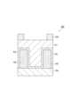
図1に示す方法MTは、半導体デバイスの製造方法に適用される基板処理方法の一つの例示的実施形態であり、酸化シリコンの領域をエッチングする方法である。この方法は、酸化シリコンから構成された第1領域と窒化シリコンから構成された第2領域とを有する基板に適用され得る。具体的には、例えば、コンタクトホールを自己整合的に形成する場合(SAC:Self-Aligned Contact)に適用され得る。The method MT shown in FIG. 1 is one exemplary embodiment of a substrate processing method applied to a method of manufacturing a semiconductor device, and is a method of etching a region of silicon oxide. This method can be applied to a substrate having a first region composed of silicon oxide and a second region composed of silicon nitride. Specifically, it can be applied, for example, to forming contact holes in a self-aligned manner (SAC: Self-Aligned Contact).
以下ではまず、図2を参照して方法MTの実行に用いることができるプラズマ処理装置1について説明する。図2に示すプラズマ処理装置1は、容量結合型プラズマエッチング装置である。In the following, a plasma processing apparatus 1 that can be used to implement method MT will first be described with reference to FIG. The plasma processing apparatus 1 shown in FIG. 2 is a capacitively coupled plasma etching apparatus.
プラズマ処理装置1は、チャンバ10を備える。チャンバ10は、その中に内部空間10sを提供する。チャンバ10はチャンバ本体12を含む。チャンバ本体12は、略円筒形状を有する。The plasma processing apparatus 1 includes a
チャンバ本体12は、例えばアルミニウムから形成される。チャンバ本体12の内壁面上には、耐腐食性を有する膜が設けられている。当該膜は、酸化アルミニウム、酸化イットリウムなどのセラミックであってよい。The
チャンバ本体12の側壁には、通路12pが形成されている。基板Wは、通路12pを通して内部空間10sとチャンバ10の外部との間で搬送される。通路12pは、チャンバ本体12の側壁に沿って設けられるゲートバルブ12gにより開閉される。A
チャンバ本体12の底部上には、支持部13が設けられている。支持部13は、絶縁材料から形成される。支持部13は、略円筒形状を有する。支持部13は、内部空間10sの中で、チャンバ本体12の底部から上方に延在している。支持部13は、上部に支持台14を有する。A
支持台14は、内部空間10sの中において、基板Wを支持するように構成されている。支持台14は、下部電極18及び静電チャック20を有する。支持台14は、電極プレート16を更に有し得る。電極プレート16は、アルミニウムなどの導体から形成され、略円盤形状を有する。The support stand 14 is configured to support the substrate W in the
下部電極18は、電極プレート16上に設けられている。下部電極18は、アルミニウムなどの導体から形成されて、略円盤形状を有する。下部電極18は、電極プレート16に電気的に接続されている。The
静電チャック20は、下部電極18上に設けられている。静電チャック20の上面に基板Wが載置される。静電チャック20は、本体及び電極を有する。静電チャック20の本体は、略円盤形状を有し、誘電体から形成される。静電チャック20の電極は、膜状の電極であり、静電チャック20の本体内に設けられている。
静電チャック20の電極は、スイッチ20sを介して直流電源20pに接続されている。静電チャック20の電極に直流電源20pからの電圧が印加されると、静電チャック20と基板Wとの間に静電引力が発生する。その静電引力により、基板Wが静電チャック20に保持される。The electrode of the
下部電極18の周縁部上には、基板Wのエッジを囲むように、エッジリング25が配置される。エッジリング25は、基板Wに対するプラズマ処理の面内均一性を向上させる。エッジリング25は、シリコン、炭化シリコン、又は石英などから形成され得る。An
下部電極18の内部には、流路18fが設けられている。流路18fには、チャンバ10の外部に設けられているチラーユニット(図示しない)から配管22aを介して熱交換媒体(例えば冷媒)が供給される。A
流路18fに供給された熱交換媒体は、配管22bを介してチラーユニットに戻される。プラズマ処理装置1では、静電チャック20上に載置された基板Wの温度が、熱交換媒体と下部電極18との熱交換により、調整される。The heat exchange medium supplied to the
プラズマ処理装置1には、ガス供給ライン24が設けられている。ガス供給ライン24は、伝熱ガス供給機構からの伝熱ガス(例えばHeガス)を、静電チャック20の上面と基板Wの裏面との間に供給する。The plasma processing apparatus 1 is provided with a
プラズマ処理装置1は、上部電極30を更に備える。上部電極30は、支持台14の上方に設けられている。上部電極30は、部材32を介して、チャンバ本体12の上部に支持されている。The plasma processing apparatus 1 further includes an
部材32は、絶縁性を有する材料から形成される。上部電極30と部材32は、チャンバ本体12の上部開口を閉じている。The
上部電極30は、天板34及び支持体36を含み得る。天板34の下面は、内部空間10sの側の下面であり、内部空間10sを画成する。天板34は、発生するジュール熱の少ない低抵抗の導電体又は半導体から形成され得る。天板34は、天板34をその板厚方向に貫通する複数のガス吐出孔34aを有する。The
支持体36は、天板34を着脱自在に支持する。支持体36は、アルミニウムなどの導電性材料から形成される。支持体36の内部には、ガス拡散室36aが設けられている。支持体36は、ガス拡散室36aから下方に延びる複数のガス孔36bを有する。The
複数のガス孔36bは、複数のガス吐出孔34aにそれぞれ連通している。支持体36には、ガス導入口36cが形成されている。ガス導入口36cは、ガス拡散室36aに接続している。ガス導入口36cには、ガス供給管38が接続されている。The plurality of
ガス供給管38には、バルブ群41、流量制御器群42、及びガスソース群40が接続されている。ガスソース群40、バルブ群41、及び流量制御器群42、は、ガス供給部を構成している。ガスソース群40は、後述する第1処理ガス及び第2処理ガスをチャンバ10に供給するように構成される。A
ガスソース群40は、複数のガスソースを含む。バルブ群41は、複数の開閉バルブを含む。流量制御器群42は、複数の流量制御器を含む。流量制御器群42の複数の流量制御器の各々は、マスフローコントローラ又は圧力制御式の流量制御器である。
ガスソース群40の複数のガスソースの各々は、バルブ群41の対応の開閉バルブ、及び流量制御器群42の対応の流量制御器を介して、ガス供給管38に接続されている。Each of the plurality of gas sources in the
プラズマ処理装置1では、チャンバ本体12の内壁面及び支持部13の外周に沿って、シールド46が着脱自在に設けられている。シールド46は、チャンバ本体12に反応副生物が付着することを防止する。In the plasma processing apparatus 1 , a
シールド46は、例えば、アルミニウムから形成された母材の表面に耐腐食性を有する膜を形成することにより構成される。耐腐食性を有する膜は、酸化イットリウムなどのセラミックから形成され得る。The
支持部13とチャンバ本体12の側壁との間には、バッフルプレート48が設けられている。バッフルプレート48は、例えば、アルミニウムから形成された母材の表面に耐腐食性を有する膜(酸化イットリウムなどの膜)を形成することにより構成される。A
バッフルプレート48には、複数の貫通孔が形成されている。バッフルプレート48の下方、且つ、チャンバ本体12の底部には、排気口12eが設けられている。A plurality of through holes are formed in the
排気口12eには、排気管52を介して排気装置50が接続されている。排気装置50は、圧力調整弁及びターボ分子ポンプなどの真空ポンプを含む。An
プラズマ処理装置1は、第1の高周波電源62及び第2の高周波電源64を備えている。第1の高周波電源62は、第1の高周波電力を発生する電源である。第1の高周波電源62は、ガスソース群40によってチャンバ10に供給される第1処理ガス及び第2処理ガスをプラズマ励起させるように構成される。The plasma processing apparatus 1 includes a first high
第1の高周波電力は、プラズマの生成に適した周波数を有する。第1の高周波電力の周波数は、例えば27[MHz]~100[MHz]の範囲内の周波数である。第1の高周波電源62は、整合器66及び電極プレート16を介して上部電極30に接続されている。The first high frequency power has a frequency suitable for plasma generation. The frequency of the first high-frequency power is, for example, within the range of 27 [MHz] to 100 [MHz]. The first high
整合器66は、第1の高周波電源62の出力インピーダンスと負荷側(上部電極30側)のインピーダンスを整合させるための回路を有する。なお、第1の高周波電源62は、整合器66を介して、下部電極18に接続されていてもよい。第1の高周波電源62は、一例のプラズマ生成部を構成している。The
第2の高周波電源64は、第2の高周波電力を発生する電源である。第2の高周波電力は、第1の高周波電力の周波数よりも低い周波数を有する。第1の高周波電力と共に第2の高周波電力が用いられる場合には、第2の高周波電力は基板Wにイオンを引き込むためのバイアス用の高周波電力として用いられる。The second high
第2の高周波電力の周波数は、例えば400[kHz]~13.56[MHz]の範囲内の周波数である。第2の高周波電源64は、整合器68及び電極プレート16を介して下部電極18に接続されている。整合器68は、第2の高周波電源64の出力インピーダンスと負荷側(下部電極18側)のインピーダンスを整合させるための回路を有する。The frequency of the second high-frequency power is, for example, within the range of 400 [kHz] to 13.56 [MHz]. The second high
なお、第1の高周波電力を用いずに、第2の高周波電力を用いて、即ち、単一の高周波電力のみを用いてプラズマを生成してもよい。この場合には、第2の高周波電力の周波数は、13.56[MHz]よりも大きな周波数、例えば40[MHz]であってもよい。Note that plasma may be generated using the second high frequency power without using the first high frequency power, that is, using only a single high frequency power. In this case, the frequency of the second high-frequency power may be higher than 13.56 [MHz], for example, 40 [MHz].
プラズマ処理装置1は、第1の高周波電源62及び整合器66を備えなくてもよい。第2の高周波電源64は一例のプラズマ生成部を構成する。The plasma processing apparatus 1 does not need to include the first high-
プラズマ処理装置1においてガスが、ガス供給部から内部空間10sに供給されて、プラズマを生成する。また、第1の高周波電力及び/又は第2の高周波電力が供給されることにより、上部電極30と下部電極18との間で高周波電界が生成される。生成された高周波電界がプラズマを生成する。In the plasma processing apparatus 1, gas is supplied from the gas supply section to the
プラズマ処理装置1は、制御部80を更に備え得る。制御部80は、プロセッサ、メモリなどの記憶部、入力装置、表示装置、信号の入出力インターフェイス等を備えるコンピュータであり得る。The plasma processing apparatus 1 may further include a
制御部80は、プラズマ処理装置1の各部を制御する。制御部80では、入力装置を用いて、オペレータがプラズマ処理装置1を管理するためにコマンドの入力操作等を行うことができる。また、制御部80では、表示装置により、プラズマ処理装置1の稼働状況を可視化して表示することができる。The
更に、記憶部には、制御プログラム及びレシピデータが格納されている。制御プログラムは、プラズマ処理装置1で各種処理を実行するために、プロセッサによって実行される。プロセッサが、制御プログラムを実行し、レシピデータに従ってプラズマ処理装置1の各部を制御する。Furthermore, the storage unit stores control programs and recipe data. The control program is executed by the processor in order to execute various processes in the plasma processing apparatus 1. A processor executes a control program and controls each part of the plasma processing apparatus 1 according to recipe data.
制御部80は、特に、ガスソース群40、第1の高周波電源62等を制御するように構成される。制御部80は、ガスソース群40、第1の高周波電源62等を制御することによって、図1のフローチャートに示す方法MTを実行する。The
より具体的に例えば、後述するように(図1に示す方法MTを参照)、制御部80は、図3に示す酸化シリコンを含む第1領域R1及び窒化シリコンを含む第2領域R2を有する基板Wを、チャンバ10内に提供する。この後、制御部80は、第1処理ガスから第1プラズマを生成することによって第1領域R1上に堆積物DPを形成するように、ガスソース群40及び第1の高周波電源62を制御するように構成される。制御部80によって実行される方法MTについては、下記に示される。More specifically, for example, as described later (see method MT shown in FIG. 1), the
以下、図1を参照して、方法MTについて詳細に説明する。方法MTは、工程ST1、工程ST2、工程ST3、及び工程ST4を含む。方法MTは、工程ST2及び工程ST3を交互に繰り返すことによって、酸化シリコンのエッチングを良好な選択比で進行させ得る。The method MT will be explained in detail below with reference to FIG. Method MT includes step ST1, step ST2, step ST3, and step ST4. In method MT, etching of silicon oxide can proceed with a good selectivity by repeating steps ST2 and ST3 alternately.
一実施形態において、方法MTは、図3に示す基板Wを処理対象として、基板Wの一部領域を選択的にエッチングすることができる。具体的に、図3に示す基板Wは、基板SB、第1領域R1、及び、第2領域R2を有している。基板SBは、第1領域R1及び第2領域R2の下地基板である。In one embodiment, the method MT can selectively etch a partial region of the substrate W, using the substrate W shown in FIG. 3 as the processing target. Specifically, the substrate W shown in FIG. 3 has a substrate SB, a first region R1, and a second region R2. The substrate SB is a base substrate for the first region R1 and the second region R2.
第1領域R1は酸化シリコンを含み、第2領域R2は窒化シリコンを含む。一実施形態において、第1領域R1は酸化シリコン(SiO2)であり、第2領域R2は窒化シリコン(Si3N4)である。The first region R1 includes silicon oxide, and the second region R2 includes silicon nitride. In one embodiment, the first region R1 is silicon oxide (SiO2 ) andthe second region R2 is silicon nitride (Si3N4 ).
第1領域R1及び第2領域R2は、プラズマに同時に晒される領域である。方法MTは、一実施形態において、第2領域R2に対して第1領域R1を選択的にエッチングするために実施される。以下、図3に示す基板Wを処理対象として想定し、方法MTについて説明する。The first region R1 and the second region R2 are regions that are simultaneously exposed to plasma. The method MT is performed in one embodiment to selectively etch the first region R1 with respect to the second region R2. Hereinafter, the method MT will be explained assuming that the substrate W shown in FIG. 3 is the processing target.
工程ST1では、チャンバ10内に第1領域R1及び第2領域R2を有する基板Wを提供する。In step ST1, a substrate W having a first region R1 and a second region R2 is provided in the
工程ST1に続く工程ST2では、第1処理ガスの第1プラズマに基板Wが晒される。より具体的に、工程ST2では、第1処理ガスが励起されることによって第1プラズマが生成され、生成された第1プラズマに基板Wが晒される。工程ST2は、第1プラズマを生成することによって、第1領域R1及び第2領域R2上に堆積物DP(堆積膜)を形成する。工程ST2の実行時のプラズマ処理装置1の各部の動作は、制御部80によって制御され得る。In step ST2 following step ST1, the substrate W is exposed to a first plasma of a first processing gas. More specifically, in step ST2, first plasma is generated by exciting the first processing gas, and the substrate W is exposed to the generated first plasma. In step ST2, a deposit DP (deposited film) is formed on the first region R1 and the second region R2 by generating a first plasma. The operation of each part of the plasma processing apparatus 1 during execution of step ST2 may be controlled by the
第1プラズマは、第1処理ガスから生成される。第1処理ガスは、炭素原子及びフッ素原子を含有する第1ガスとケイ素原子を含有する第2ガスとを含む混合ガスである。堆積物DPは、炭素原子及びフッ素原子を含有する。A first plasma is generated from a first processing gas. The first processing gas is a mixed gas containing a first gas containing carbon atoms and fluorine atoms and a second gas containing silicon atoms. Deposit DP contains carbon atoms and fluorine atoms.
第1ガスは、フルオロカーボンガス及び/又はハイドロフルオロカーボンガスである。第1ガスは、例えば、C5F8ガス、C3F8ガス、C4F8ガス、C5F8ガス、C4F6ガス、CF4ガス、CH3Fガス、CHF3ガス、CH2F2ガスの群から選択される少なくとも一種類を含む。第1ガスは、Arガス、Heガス等の種々の希ガスのうち少なくとも一種類を更に含み得る。第1ガスは、O2ガスを更に含み得る。The first gas is a fluorocarbon gas and/or a hydrofluorocarbon gas. The first gasis , for example,C5F8 gas,C3F8 gas,C4F8 gas,C5F8 gas, C4F6gas,CF4 gas,CH3F gas,CHF3 gas, Contains at least one type selected from the group of CH2 F2 gases. The first gas may further include at least one kind of various rare gases such as Ar gas and He gas. The first gas may further include O2 gas.
第2ガスは、例えば、SiCl4ガス、SiH4ガス、Si2H6ガス、SiH2Cl2ガス、Si4H10ガス、Si5H12ガスの群から選択される少なくとも一種類を含む。The second gas includes, for example, at least one type selected from the group of SiCl4 gas, SiH4 gas, Si2 H6 gas, SiH2 Cl2 gas, Si4 H10 gas, and Si5 H12 gas.
プラズマ処理装置1を用いて工程ST2を実行する場合には、ガスソース群40からチャンバ本体12内に第1処理ガスが供給される。工程ST2では、第1の高周波電源62からの高周波電力が上部電極30に供給される。工程ST2では、第2の高周波電源64からの高周波バイアス電力が下部電極18に供給され得る。When performing step ST2 using the plasma processing apparatus 1, the first processing gas is supplied into the
工程ST2では、排気装置50によってチャンバ本体12の内部空間10sの圧力が所定の圧力に設定される。In step ST2, the
以上のように、チャンバ本体12内において第1処理ガスから第1プラズマが生成され、支持台14上に載置された基板Wが第1プラズマに晒される。このため、炭素原子及びフッ素原子(フルオロカーボン)を含有する堆積物が第1領域R1に付着する。従って、フルオロカーボンを含む堆積物DPが第1領域R1及び第2領域R2上に形成される。この結果、後述する工程ST3において、堆積物DPによって第2領域R2が保護されつつ、第1領域R1のエッチングが進行することが可能となる。As described above, the first plasma is generated from the first processing gas in the
上述したように、第1処理ガスにケイ素原子を含有する第2ガスが含まれる。このため、第1処理ガスから第1プラズマを生成した際、下記式(1)に示す反応により、プラズマ気相中で過剰なフッ素原子がケイ素原子と反応して除去される。
Si+4F→SiF4↑ (1)
結果として、第1領域R1及び第2領域R2上にフッ素原子の組成比に対する炭素原子の組成比の比率(C/F比)が高い堆積物DPを形成することができる。なお、工程ST2において第1ガス及び第2ガスの流量比を調整することによって、堆積物DPのC/F比を制御することが可能である。例えば、第1ガスに対する第2ガスの流量比を大きくすることで、堆積物DPのC/F比を大きくすることができる。As described above, the first processing gas includes the second gas containing silicon atoms. Therefore, when the first plasma is generated from the first processing gas, excess fluorine atoms react with silicon atoms in the plasma gas phase and are removed by the reaction shown in equation (1) below.
Si+4F→SiF4↑ (1)
As a result, a deposit DP having a high ratio of the composition ratio of carbon atoms to the composition ratio of fluorine atoms (C/F ratio) can be formed on the first region R1 and the second region R2. Note that it is possible to control the C/F ratio of the deposit DP by adjusting the flow rate ratio of the first gas and the second gas in step ST2. For example, by increasing the flow rate ratio of the second gas to the first gas, the C/F ratio of the deposit DP can be increased.
工程ST2に引き続く工程ST3では、第2プラズマを生成することによって第1領域R1をエッチングする。より具体的に、堆積物DPに含まれるフルオロカーボンのラジカルによって第1領域R1がエッチングされる。工程ST3の実行時のプラズマ処理装置1の各部の動作は、制御部80によって制御され得る。In step ST3 following step ST2, the first region R1 is etched by generating second plasma. More specifically, the first region R1 is etched by fluorocarbon radicals contained in the deposit DP. The operation of each part of the plasma processing apparatus 1 during execution of step ST3 may be controlled by the
第2プラズマは第2処理ガスから生成され、第2処理ガスは不活性ガスを含む。工程ST3では、工程ST2の処理後の基板Wが、不活性ガスのプラズマに晒される。工程ST3において用いられる不活性ガスは、希ガス又は窒素ガスであり得る。A second plasma is generated from a second processing gas, and the second processing gas includes an inert gas. In step ST3, the substrate W processed in step ST2 is exposed to inert gas plasma. The inert gas used in step ST3 may be a rare gas or nitrogen gas.
工程ST2の処理時間と工程ST3の処理時間とは任意に設定される。一実施形態においては、工程ST2の処理時間と工程ST3の処理時間との合計において工程ST2の処理時間が占める割合は、例えば5~45%の範囲内の割合に設定される。The processing time of step ST2 and the processing time of step ST3 are arbitrarily set. In one embodiment, the proportion of the processing time of step ST2 in the total of the processing time of step ST2 and the processing time of step ST3 is set, for example, to a ratio within a range of 5 to 45%.
プラズマ処理装置1を用いて工程ST3を実行する場合には、ガスソース群40から不活性ガスが供給される。工程ST3では、不活性ガスに加えてO2ガスが供給されてもよい。When performing step ST3 using the plasma processing apparatus 1, inert gas is supplied from the
工程ST3では、第1の高周波電源62からの高周波電力が上部電極30に供給される。工程ST3では、第2の高周波電源64からの高周波バイアス電力が下部電極18に供給され得る。In step ST3, high frequency power from the first high
工程ST3では、排気装置50によってチャンバ本体12内の空間の圧力が所定の圧力に設定される。In step ST3, the pressure in the space within the
方法MTでは、工程ST3の実行の後、再び、工程ST2が実行される(工程ST4:NO)。このように、工程ST2及び工程ST3を含むサイクルが一回以上実行され得る。先の工程ST3の実行によって堆積物DPの膜厚が減少しているので、再び工程ST2を実行して上述した第1処理ガスの第1プラズマに基板Wを晒すと、第1領域R1を更にエッチングすることができる。その後、更に工程ST3を実行することで、堆積物DP中のフルオロカーボンラジカルにより第1領域R1をエッチングすることができる。In method MT, after performing step ST3, step ST2 is performed again (step ST4: NO). In this way, a cycle including step ST2 and step ST3 may be executed more than once. Since the film thickness of the deposit DP has been reduced by performing the previous step ST3, when the step ST2 is performed again and the substrate W is exposed to the first plasma of the first processing gas described above, the first region R1 is further reduced. Can be etched. Thereafter, by further performing step ST3, the first region R1 can be etched by the fluorocarbon radicals in the deposit DP.
方法MTでは、工程ST4において停止条件が満たされるか否かが判定される。停止条件は、例えば、工程ST2及び工程ST3を含むサイクルの繰り返し回数が所定回数に達したときに満たされたものと判定される。停止条件が満たされない場合(工程ST4:NO)には、工程ST2及び工程ST3を含むサイクルが再び実行される。一方、停止条件が満たされる場合(工程ST4:YES)には、方法MTが終了する。In method MT, it is determined in step ST4 whether a stop condition is satisfied. The stop condition is determined to be satisfied, for example, when the number of repetitions of the cycle including step ST2 and step ST3 reaches a predetermined number of times. If the stop condition is not satisfied (step ST4: NO), the cycle including step ST2 and step ST3 is executed again. On the other hand, if the stop condition is satisfied (step ST4: YES), the method MT ends.
以上説明した方法MTでは、工程ST2及び工程ST3を交互に複数回実行することにより、高い選択比で第2領域R2に対して第1領域R1を選択的にエッチングすることができる。In the method MT described above, the first region R1 can be selectively etched with respect to the second region R2 with a high selection ratio by alternately performing the steps ST2 and ST3 a plurality of times.
図4は、方法MTの処理対象の別の一例を示す断面図である。図4に示す基板は、第1領域R1及び第2領域R2を有する基板W2であり、基板W2に対して方法MTを用いることができる。具体的に、基板W2は、下地層100、複数の隆起領域102、第1領域R1、第2領域R2、及び、マスク108を有している。基板W2は、例えば、フィン型電界効果トランジスタの製造中に得られる生産物である。FIG. 4 is a cross-sectional view showing another example of the processing target of method MT. The substrate shown in FIG. 4 is a substrate W2 having a first region R1 and a second region R2, and method MT can be used for the substrate W2. Specifically, the substrate W2 includes a
下地層100は、例えば、多結晶シリコンから構成される。下地層は、一例においてはフィン領域であり、略直方体形状を有している。
複数の隆起領域102は、下地層100上に設けられており、互いに略平行に配列されている。隆起領域102は、例えば、ゲート領域である。The plurality of raised
第2領域R2の材料は、窒化シリコンである。第2領域R2は、隆起領域102を覆うように設けられている。The material of the second region R2 is silicon nitride. The second region R2 is provided to cover the raised
隆起領域102は、第1領域R1内に埋め込まれている。即ち、第1領域R1は、第2領域R2を介して隆起領域102を覆うように設けられている。The raised
第1領域R1の材料は、酸化シリコンである。第1領域R1上には、マスク108が設けられている。マスク108は、隣接する隆起領域102間の上方において開口するパターンを有している。マスク108は、有機膜である。マスク108は、フォトリソグラフィによって作成され得る。The material of the first region R1 is silicon oxide. A
基板W2に対して方法MTを実行すると、基板W2の第1領域R1を第2領域R2に対して選択的にエッチングすることができる。隣接する二つの隆起領域102の間の領域においてホールを自己整合的に形成することができる(SAC)。当該ホールは、例えば、フィン領域のソース又はドレインに接続するコンタクト用のホールとなり得る。When the method MT is performed on the substrate W2, the first region R1 of the substrate W2 can be etched selectively with respect to the second region R2. Holes can be formed in a self-aligned manner in the region between two adjacent raised regions 102 (SAC). The hole can be, for example, a contact hole connected to the source or drain of the fin region.
より具体的に、工程ST1において、図4に示す基板W2がチャンバ10内に提供される。工程ST1に引き続き、上述した工程ST2が実行される。工程ST2で用いられる第1処理ガスは、第1処理ガスについて上述したガス種のガスである。工程ST2で用いられる内部空間10sの圧力は、工程ST2における内部空間10sの圧力について上述した圧力である。工程ST2の実行によって、基板W2の第1領域R1上に堆積物DPが形成される。More specifically, in step ST1, a substrate W2 shown in FIG. 4 is provided in the
工程ST2に引き続き、上述した工程ST3が実行される。工程ST3で用いられる第2処理ガスは、第2処理ガスについて上述したガス種のガスである。工程ST3で用いられる内部空間10sの圧力は、工程ST3における内部空間10sの圧力について上述した圧力である。工程ST3の実行によって、基板W2上に形成された堆積物DP中のフルオロカーボンラジカルが、基板W2の第1領域R1のエッチングを進行させる。Following step ST2, step ST3 described above is executed. The second processing gas used in step ST3 is the type of gas described above for the second processing gas. The pressure in the
基板W2に対し、上述した工程ST4において停止条件が満たされないと判定された場合(工程ST4:NO)、工程ST3の実行の後に再び工程ST2が実行される。このように、基板W2に対し工程ST2及び工程ST3を含むサイクルが一回以上実行され得る。If it is determined that the stop condition is not satisfied in step ST4 described above for substrate W2 (step ST4: NO), step ST2 is performed again after step ST3 is performed. In this way, a cycle including step ST2 and step ST3 may be performed on the substrate W2 more than once.
以上説明したように基板W2に対して工程ST2及び工程ST3が繰り返し実行されることによって、図5に示すように、マスク108のパターンに沿って第1領域R1が第2領域R2に至るまでエッチングされる。As explained above, by repeatedly performing steps ST2 and ST3 on the substrate W2, as shown in FIG. 5, the first region R1 is etched until it reaches the second region R2 along the pattern of the
工程ST2及び工程ST3が繰り返し実行されることによって第2領域R2が露出されると、工程ST2によって第2領域R2上に堆積物DPが形成され、第2領域R2が堆積物DPによってエッチングから保護される。When the second region R2 is exposed by repeatedly performing steps ST2 and ST3, a deposit DP is formed on the second region R2 in the step ST2, and the second region R2 is protected from etching by the deposit DP. be done.
更に工程ST2及び工程ST3が繰り返し実行されることによって、図6に示すように、隣接する二つの隆起領域102の間の第1領域R1が,第2領域R2によって画定される凹部の底面に至るまで、第2領域R2に対して選択的にエッチングされる。隆起領域102は、第2領域R2上の堆積物DPによってエッチングから保護される。Furthermore, by repeatedly performing steps ST2 and ST3, as shown in FIG. 6, the first region R1 between two adjacent raised
以下、方法MTの評価のために行った複数の実験例について説明する。以下に説明する複数の実験例は、単に方法MTを例示するために示されるものであり、方法MTを限定するものではない。Hereinafter, a plurality of experimental examples conducted for evaluating method MT will be described. The experimental examples described below are presented merely to illustrate method MT, and are not intended to limit method MT.
方法MTに係る複数の実験例では、レジスト膜を表面に有する基板上に30[mm]角のSiO2チップ(酸化シリコン膜)及び30[mm]角のSiNチップ(窒化シリコン膜)を貼り付けた構造を有する基板を準備した。SiO2チップは第1領域R1に対応し、SiNチップは第2領域R2に対応する。これら二つのチップを基板の中心から均等な距離に貼り付けた。この基板に対して、以下に記す処理条件のもとで複数の実験例の処理を行った。In several experimental examples related to method MT, a 30 [mm] square SiO2 chip (silicon oxide film) and a 30 [mm] square SiN chip (silicon nitride film) were pasted on a substrate with a resist film on the surface. A substrate having a structure was prepared. The SiO2 chip corresponds to the first region R1, and the SiN chip corresponds to the second region R2. These two chips were attached at equal distances from the center of the board. This substrate was subjected to processing in a plurality of experimental examples under the processing conditions described below.
複数の実験例では、2秒間の工程ST2と、N秒間(Nは正の整数)の工程ST3とを含むサイクルが30回実行された。複数の実験例において、工程ST3の実行時間(N秒間)は、5~25秒間における何れかの時間(5≦N≦25)である(図7の横軸を参照)。複数の実験例は、工程ST3の実行時間の相違のみにおいて、互いに相違する。In several experimental examples, a cycle including step ST2 for 2 seconds and step ST3 for N seconds (N is a positive integer) was performed 30 times. In a plurality of experimental examples, the execution time (N seconds) of step ST3 is any time between 5 and 25 seconds (5≦N≦25) (see the horizontal axis in FIG. 7). The plurality of experimental examples differ from each other only in the execution time of step ST3.
工程ST2で用いられる第1処理ガスの第1ガスは、C4F6ガス及びArガスの混合ガスである。工程ST2で用いられる第1処理ガスの第2ガスは、SiCl4ガスである。工程ST2の処理条件は、圧力:20[mTorr]、C4F6ガス流量:4[sccm]、Arガス流量:1188[sccm]、SiCl4ガス流量:2[sccm]、である。工程ST2の処理条件は、更に、第1の高周波電源62の高周波電力:60[MHz],100[W]、第2の高周波電源64の高周波バイアス電力:40[MHz],150[W]、直流電圧:-300[V]、である。The first processing gas used in step ST2 is a mixed gas of C4 F6 gas and Ar gas. The second gas of the first processing gas used in step ST2 is SiCl4 gas. The processing conditions of step ST2 are pressure: 20 [mTorr], C4 F6 gas flow rate: 4 [sccm], Ar gas flow rate: 1188 [sccm], and SiCl4 gas flow rate: 2 [sccm]. The processing conditions of step ST2 are as follows: high frequency power of the first high frequency power supply 62: 60 [MHz], 100 [W]; high frequency bias power of the second high frequency power supply 64: 40 [MHz], 150 [W]; DC voltage: -300 [V].
工程ST3で用いられる第2処理ガスの不活性ガスは、Arガスである。工程ST3の処理条件は、圧力:20[mTorr]、Arガス流量:1188[sccm]、である。工程ST3の処理条件は、更に、第1の高周波電源62の高周波電力:60[MHz],100[W]、第2の高周波電源64の高周波バイアス電力:40[MHz],150[W]、直流電圧:0[V]、である。The inert gas of the second processing gas used in step ST3 is Ar gas. The processing conditions of step ST3 are pressure: 20 [mTorr], Ar gas flow rate: 1188 [sccm]. The processing conditions of step ST3 are as follows: high frequency power of the first high frequency power supply 62: 60 [MHz], 100 [W]; high frequency bias power of the second high frequency power supply 64: 40 [MHz], 150 [W]; DC voltage: 0 [V].
図7に、上記の複数の実験例によって得られた結果に関するグラフを示す。図7には、工程ST3におけるSiO2チップのエッチング量とSiNチップのエッチング量とが示されている。図7の横軸は、工程ST3の合計処理時間を示している。FIG. 7 shows a graph regarding the results obtained from the plurality of experimental examples described above. FIG. 7 shows the etching amount of the SiO2 chip and the etching amount of the SiN chip in step ST3. The horizontal axis in FIG. 7 indicates the total processing time of step ST3.
図7の左側の縦軸は、工程ST3におけるSiO2チップのエッチング量を示している。図7のPT1aは、SiO2チップのエッチング量の測定結果を示している。図7の右側の縦軸は、工程ST3におけるSiNチップのエッチング量を示している。図7のPT2aは、SiNチップのエッチング量の測定結果を示している。The vertical axis on the left side of FIG. 7 indicates the amount of etching of the SiO2 chip in step ST3. PT1a in FIG. 7 shows the measurement results of the etching amount of the SiO2 chip. The vertical axis on the right side of FIG. 7 indicates the amount of etching of the SiN chip in step ST3. PT2a in FIG. 7 shows the measurement results of the etching amount of the SiN chip.
なお、図8には、図7に示す実験例(方法MTに係る実験例)に対応する実験例によって得られた結果が示されている。図8の実験例では、図7の実験例の工程ST2及び工程ST3のそれぞれに対応する二つの工程が行われた。Note that FIG. 8 shows results obtained by an experimental example corresponding to the experimental example shown in FIG. 7 (experimental example related to method MT). In the experimental example of FIG. 8, two processes corresponding to each of process ST2 and process ST3 of the experimental example of FIG. 7 were performed.
図8の実験例の二つの工程のうち工程ST2に対応する工程(以下、工程ST2aという)では、SiCl4ガスを含まない処理ガス(即ちC4F6ガス及びArガスのみを含む処理ガス)が用いられた。図8の実験例は、この点についてのみ図7の実験例と相違する。In the step corresponding to step ST2 (hereinafter referred to as step ST2a) of the two steps in the experimental example in FIG. 8, a processing gas that does not contain SiCl4 gas (that is, a processing gas that contains only C4 F6 gas and Ar gas) is used. was used. The experimental example shown in FIG. 8 differs from the experimental example shown in FIG. 7 only in this respect.
図8の横軸、左側の縦軸、及び右側の縦軸は、図7と同様である。図8のPT1bは、SiO2チップのエッチング量の測定結果を示している。図8のPT2bは、SiNチップのエッチング量の測定結果を示している。The horizontal axis, left vertical axis, and right vertical axis in FIG. 8 are the same as those in FIG. 7. PT1b in FIG. 8 shows the measurement results of the etching amount of the SiO2 chip. PT2b in FIG. 8 shows the measurement results of the etching amount of the SiN chip.
図7に示すように、図7の実験例及び図8の実験例の何れにおいても、工程ST3の合計処理時間が長くなるにつれて、SiO2チップのエッチング量は増加し、SiNチップのエッチング量は少ない量で一定のままであるという結果が得られた。As shown in FIG. 7, in both the experimental example of FIG. 7 and the experimental example of FIG. The result was that it remained constant at a small amount.
更に、SiNチップのエッチング量の平均値は、図7に示す場合に2.3[nm]であり、図8に示す場合に3.1[nm]であった。即ち、工程ST2においてSiCl4ガスが用いられる実験例では、工程ST2aにおいてSiCl4ガスが用いられない実験例に比較して、SiNチップのエッチング量は少ない。Furthermore, the average value of the etching amount of the SiN chip was 2.3 [nm] in the case shown in FIG. 7, and 3.1 [nm] in the case shown in FIG. 8. That is, in the experimental example in which SiCl4 gas is used in step ST2, the amount of etching of the SiN chip is smaller than in the experimental example in which SiCl4 gas is not used in step ST2a.
従って、方法MTによれば、比較的高い選択比でSiNの第2領域R2に対してSiO2の第1領域R1を選択的にエッチングすることができる。この結果は、図9に示す結果によって裏付けられ得る。Therefore, according to method MT, the first region R1 of SiO2 can be selectively etched with respect to the second region R2 of SiN with a relatively high selectivity. This result can be supported by the results shown in FIG.
図9には、90秒間の工程ST2及び90秒間の工程ST2aの実行によってSiNチップ(第2領域R2に対応)上にそれぞれ形成された堆積物DPの原子組成%が示されている。FIG. 9 shows the atomic composition percentages of the deposits DP formed on the SiN chip (corresponding to the second region R2) by performing step ST2 for 90 seconds and step ST2a for 90 seconds.
図9の縦軸は、原子組成%を示している。図9に示すGF1aは、90秒間の工程ST2a(C4F6ガス及びArガスの混合ガスが第1処理ガスに用いられる場合)による結果を示している。図9に示すGF2aは、90秒間の工程ST2(C4F6ガス、Arガス及びSiCl4ガスの混合ガスが第1処理ガスに用いられる場合)による結果を示している。The vertical axis in FIG. 9 indicates atomic composition %. GF1a shown in FIG. 9 shows the result of step ST2a (when a mixed gas of C4 F6 gas and Ar gas is used as the first processing gas) for 90 seconds. GF2a shown in FIG. 9 shows the result of step ST2 for 90 seconds (when a mixed gas of C4 F6 gas, Ar gas, and SiCl4 gas is used as the first processing gas).
図9に示す結果によれば、工程ST2においてSiCl4ガスが用いられる実験例の方が、工程ST2aにおいてSiCl4ガスが用いられない実験例に比較して、堆積物DPにおけるC/F比が大きいことがわかる。この結果は、第1処理ガスからプラズマを生成した際、プラズマ気相中で過剰なフッ素原子がケイ素原子と反応して除去されたことによるものと考えられる。According to the results shown in FIG. 9, the C/F ratio in the deposit DP was higher in the experimental example in which SiCl4 gas was used in step ST2 than in the experimental example in which SiCl4 gas was not used in step ST2a. You can see that it's big. This result is considered to be due to the fact that when plasma was generated from the first processing gas, excess fluorine atoms were removed by reacting with silicon atoms in the plasma gas phase.
方法MTによれば、工程ST2においてSiCl4ガスが第2ガスに用いられる場合、第2ガスの流量を調整することによって第2領域R2上の堆積物DPにおけるC/F比が良好に制御される。このため、堆積物DPのエッチングに対する耐性が増加することによって、高い選択比で第2領域R2に対して第1領域R1を選択的にエッチングすることができる。According to method MT, when SiCl4 gas is used as the second gas in step ST2, the C/F ratio in the deposit DP on the second region R2 is well controlled by adjusting the flow rate of the second gas. Ru. Therefore, by increasing the etching resistance of the deposit DP, the first region R1 can be selectively etched with respect to the second region R2 with a high selection ratio.
更に、図10には、90秒間の工程ST2及び90秒間の工程ST2aの実行によってSiNチップ上にそれぞれ形成された堆積物DPの膜厚が示されている。Furthermore, FIG. 10 shows the film thicknesses of the deposits DP formed on the SiN chip by executing the process ST2 for 90 seconds and the process ST2a for 90 seconds.
図10によれば、工程ST2においてSiCl4ガスが用いられる実験例の方が、工程ST2aにおいてSiCl4ガスが用いられない実験例に比較して、SiNチップ上に形成された堆積物DPの膜厚が厚い。According to FIG. 10, the film of the deposit DP formed on the SiN chip is better in the experimental example in which SiCl4 gas is used in step ST2 than in the experimental example in which SiCl4 gas is not used in step ST2a. Thick.
以上、種々の例示的実施形態について説明してきたが、上述した例示的実施形態に限定されることなく、様々な省略、置換、及び変更がなされてもよい。また、異なる例示的実施形態における要素を組み合わせて他の例示的実施形態を形成することが可能である。Although various exemplary embodiments have been described above, various omissions, substitutions, and changes may be made without being limited to the exemplary embodiments described above. Also, elements in different exemplary embodiments may be combined to form other exemplary embodiments.
例えば、工程ST2において用いられる第2ガスの流量は、工程ST2及び工程ST3が繰り返されるごとに段階的に増減され得る。一例として、工程ST2の最初の実行時から工程ST2が繰り返されるごとに第2ガスの流量は低減される。工程ST2が繰り返されることによって第2ガスのケイ素原子のプラズマによる第2領域R2の変質領域TRからのフッ素原子の除去が進むからである。For example, the flow rate of the second gas used in step ST2 may be increased or decreased in steps each time step ST2 and step ST3 are repeated. As an example, the flow rate of the second gas is reduced each time step ST2 is repeated from the first execution of step ST2. This is because by repeating step ST2, the removal of fluorine atoms from the altered region TR of the second region R2 by the plasma of silicon atoms of the second gas progresses.
以上の説明から、本開示の種々の例示的実施形態は、説明の目的で本明細書で説明されており、本開示の範囲及び主旨から逸脱することなく種々の変更をなし得ることが、理解されるであろう。したがって、本明細書に開示した種々の例示的実施形態は限定することを意図しておらず、真の範囲と主旨は、添付の特許請求の範囲によって示される。From the foregoing description, it will be understood that various exemplary embodiments of the present disclosure are described herein for purposes of illustration, and that various changes may be made without departing from the scope and spirit of the disclosure. will be done. Therefore, the various exemplary embodiments disclosed herein are not intended to be limiting, with the true scope and spirit being indicated by the following claims.
1…プラズマ処理装置、10…チャンバ、100…下地層、102…隆起領域、108…マスク、10s…内部空間、12…チャンバ本体、12e…排気口、12g…ゲートバルブ、12p…通路、13…支持部、14…支持台、16…電極プレート、18…下部電極、18f…流路、20…静電チャック、20p…直流電源、20s…スイッチ、22a…配管、22b…配管、24…ガス供給ライン、25…エッジリング、30…上部電極、32…部材、34…天板、34a…ガス吐出孔、36…支持体、36a…ガス拡散室、36b…ガス孔、36c…ガス導入口、38…ガス供給管、40…ガスソース群、41…バルブ群、42…流量制御器群、46…シールド、48…バッフルプレート、50…排気装置、52…排気管、62…第1の高周波電源、64…第2の高周波電源、66…整合器、68…整合器、80…制御部。DESCRIPTION OF SYMBOLS 1... Plasma processing apparatus, 10... Chamber, 100... Base layer, 102... Raised area, 108... Mask, 10s... Internal space, 12... Chamber body, 12e... Exhaust port, 12g... Gate valve, 12p... Passage, 13... Support part, 14... Support stand, 16... Electrode plate, 18... Lower electrode, 18f... Channel, 20... Electrostatic chuck, 20p... DC power supply, 20s... Switch, 22a... Piping, 22b... Piping, 24... Gas supply Line, 25... Edge ring, 30... Upper electrode, 32... Member, 34... Top plate, 34a... Gas discharge hole, 36... Support body, 36a... Gas diffusion chamber, 36b... Gas hole, 36c... Gas inlet, 38 ...Gas supply pipe, 40...Gas source group, 41...Valve group, 42...Flow rate controller group, 46...Shield, 48...Baffle plate, 50...Exhaust device, 52...Exhaust pipe, 62...First high frequency power supply, 64... Second high frequency power supply, 66... Matching box, 68... Matching box, 80... Control unit.
Claims (12)
Translated fromJapaneseb)第1処理ガスから第1プラズマを生成することによって前記第1領域及び前記第2領域上に堆積膜を形成する工程と、
c)不活性ガスを含む第2処理ガスから第2プラズマを生成することによって前記第1領域をエッチングする工程と、
を備え、
前記第1処理ガスは、炭素原子及びフッ素原子を含有する第1ガスとケイ素原子を含有する第2ガスとを含む混合ガスであり、
前記c)は、前記堆積膜と前記第2プラズマに含まれるイオンとを反応させることによって、前記第1領域をエッチングする、
基板処理方法。a) providing a substrate having a first region and a second region within a chamber;
b) forming a deposited film on the first region and the second region by generating a first plasma from a first processing gas;
c) etching the first region by generating a second plasma from a second process gas including an inert gas;
Equipped with
The first processing gasis a mixed gas containing a first gas containing carbon atoms and fluorine atoms and a second gas containing silicon atoms,
c) etching the first region by causing the deposited film to react with ions contained in the second plasma;
Substrate processing method.
b)第1処理ガスから第1プラズマを生成することによって前記第1領域及び前記第2領域上に堆積膜を形成する工程と、
c)不活性ガスを含む第2処理ガスから第2プラズマを生成することによって前記第1領域をエッチングする工程と、
を備え、
前記第1処理ガスは、炭素原子及びフッ素原子を含有する第1ガスとケイ素原子を含有する第2ガスとを含む混合ガスであり、
前記堆積膜は、炭素原子及びフッ素原子を含有し、
前記b)は、前記第1ガス及び前記第2ガスの流量比を調整することによって、前記第1領域及び前記第2領域上に形成される堆積膜の炭素原子及びフッ素原子の組成比を制御する、
基板処理方法。a) providing a substrate having a first region and a second region within a chamber;
b) forming a deposited film on the first region and the second region by generating a first plasma from a first processing gas;
c) etching the first region by generating a second plasma from a second process gas including an inert gas;
Equipped with
The first processing gas is a mixed gas containing a first gas containing carbon atoms and fluorine atoms and a second gas containing silicon atoms,
The deposited film contains carbon atoms and fluorine atoms,
In b), the composition ratio of carbon atoms and fluorine atoms in the deposited film formed on the first region and the second region is controlled by adjusting the flow rate ratio of the first gas and the second gas. do,
Substrate processing method.
b)第1処理ガスから第1プラズマを生成することによって前記第1領域及び前記第2領域上に堆積膜を形成する工程と、 b) forming a deposited film on the first region and the second region by generating a first plasma from a first processing gas;
c)不活性ガスを含む第2処理ガスから第2プラズマを生成することによって前記第1領域をエッチングする工程と、 c) etching the first region by generating a second plasma from a second process gas including an inert gas;
を備え、 Equipped with
前記第1処理ガスは、炭素原子及びフッ素原子を含有する第1ガスとケイ素原子を含有する第2ガスとを含む混合ガスであり、 The first processing gas is a mixed gas containing a first gas containing carbon atoms and fluorine atoms and a second gas containing silicon atoms,
前記第2処理ガスは、希ガス又は窒素ガスである、 The second processing gas is a rare gas or nitrogen gas,
基板処理方法。 Substrate processing method.
請求項1~3の何れか一項に記載の基板処理方法。The first gas includes C5 F8 gas, C3 F8 gas, C4 F8 gas, C5 F8 gas, C4 F6 gas, CF4 gas, CH3 F gas, CHF3 gas, and CH2 F2 containing at least one selected from the group of gases;
The substrate processing method according to any one of claims 1 to 3.
請求項1~5の何れか一項に記載の基板処理方法。The second gas includes at least one type selected from the group of SiCl4 gas, SiH4 gas, Si2 H6 gas, SiH2 Cl2 gas, Si4 H10 gas, and Si5 H12 gas.
The substrate processing method according to any one of claims 1 to 5.
請求項1~6の何れか一項に記載の基板処理方法。The first region includes silicon oxide, and the second region includes silicon nitride.
The substrate processing method according to any one of claims 1 to 6.
請求項1に記載の基板処理方法。b) increases or decreases the flow rate of the second gas in steps;
The substrate processing method according to claim 1.
請求項1~8の何れか一項に記載の基板処理方法。performing a cycle including b) and c) one or more times;
The substrate processing method according toany one of claims 1 to 8 .
前記チャンバに処理ガスを供給するように構成されるガスソース群と、
前記ガスソース群によって前記チャンバに供給される前記処理ガスをプラズマ励起させるように構成される高周波電源と、
前記ガスソース群及び前記高周波電源を制御するように構成される制御部と、
を備え、
前記制御部は、
a)前記チャンバ内に第1領域及び第2領域を有する基板を提供する工程と、
b)前記処理ガスからプラズマを生成することによって前記第1領域上に堆積膜を形成する工程と、
c)不活性ガスを含む第2処理ガスから第2プラズマを生成することによって前記第1領域をエッチングする工程と、
を含む処理を実行し、
前記処理ガスは、炭素原子及びフッ素原子を含有する第1ガスとケイ素原子を含有する第2ガスとを含む混合ガスであり、
前記第2処理ガスは、希ガス又は窒素ガスである、
プラズマ処理装置。a chamber;
a group of gas sources configured to supply process gas to the chamber;
a high frequency power source configured to plasma excite the processing gas supplied to the chamber by the gas sources;
a control unit configured to control the gas source group and the high frequency power source;
Equipped with
The control unit includes:
a) providing a substrate having a first region and a second region within the chamber;
b) forming a deposited film on the first region by generating plasma from the processing gas;
c) etching the first region by generating a second plasma from a second process gas including an inert gas;
Execute processing including
The processing gasis a mixed gas containing a first gas containing carbon atoms and fluorine atoms and a second gas containing silicon atoms,
The second processing gas is a rare gas or nitrogen gas,
Plasma processing equipment.
前記チャンバに処理ガスを供給するように構成されるガスソース群と、
前記ガスソース群によって前記チャンバに供給される前記処理ガスをプラズマ励起させるように構成される高周波電源と、
前記ガスソース群及び前記高周波電源を制御するように構成される制御部と、
を備え、
前記制御部は、
a)前記チャンバ内に第1領域及び第2領域を有する基板を提供する工程と、
b)前記処理ガスからプラズマを生成することによって前記第1領域上に堆積膜を形成する工程と、
c)不活性ガスを含む第2処理ガスから第2プラズマを生成することによって前記第1領域をエッチングする工程と、
を含む処理を実行し、
前記処理ガスは、炭素原子及びフッ素原子を含有する第1ガスとケイ素原子を含有する第2ガスとを含む混合ガスであり、
前記c)は、前記堆積膜と前記第2プラズマに含まれるイオンとを反応させることによって、前記第1領域をエッチングする、
プラズマ処理装置。a chamber;
a group of gas sources configured to supply process gas to the chamber;
a high frequency power source configured to plasma excite the processing gas supplied to the chamber by the gas sources;
a control unit configured to control the gas source group and the high frequency power source;
Equipped with
The control unit includes:
a) providing a substrate having a first region and a second region within the chamber;
b) forming a deposited film on the first region by generating plasma from the processing gas;
c) etching the first region by generating a second plasma from a second process gas including an inert gas;
Execute processing including
The processing gas is a mixed gas containing a first gas containing carbon atoms and fluorine atoms and a second gas containing silicon atoms,
c) etching the first region by causing the deposited film to react with ions contained in the second plasma;
Plasma processing equipment.
Priority Applications (4)
| Application Number | Priority Date | Filing Date | Title |
|---|---|---|---|
| JP2019181487AJP7398915B2 (en) | 2019-10-01 | 2019-10-01 | Substrate processing method, semiconductor device manufacturing method, and plasma processing apparatus |
| TW109131991ATWI874452B (en) | 2019-10-01 | 2020-09-17 | Substrate processing method, method for manufacturing semiconducor device, and plasma processing apparatus |
| CN202010994040.8ACN112599414A (en) | 2019-10-01 | 2020-09-21 | Substrate processing method, semiconductor device manufacturing method, and plasma processing apparatus |
| US17/035,899US11955316B2 (en) | 2019-10-01 | 2020-09-29 | Substrate processing method, method for manufacturing semiconducor device, and plasma processing apparatus |
Applications Claiming Priority (1)
| Application Number | Priority Date | Filing Date | Title |
|---|---|---|---|
| JP2019181487AJP7398915B2 (en) | 2019-10-01 | 2019-10-01 | Substrate processing method, semiconductor device manufacturing method, and plasma processing apparatus |
Publications (2)
| Publication Number | Publication Date |
|---|---|
| JP2021057523A JP2021057523A (en) | 2021-04-08 |
| JP7398915B2true JP7398915B2 (en) | 2023-12-15 |
Family
ID=75162198
Family Applications (1)
| Application Number | Title | Priority Date | Filing Date |
|---|---|---|---|
| JP2019181487AActiveJP7398915B2 (en) | 2019-10-01 | 2019-10-01 | Substrate processing method, semiconductor device manufacturing method, and plasma processing apparatus |
Country Status (4)
| Country | Link |
|---|---|
| US (1) | US11955316B2 (en) |
| JP (1) | JP7398915B2 (en) |
| CN (1) | CN112599414A (en) |
| TW (1) | TWI874452B (en) |
Families Citing this family (2)
| Publication number | Priority date | Publication date | Assignee | Title |
|---|---|---|---|---|
| US12347645B2 (en)* | 2021-04-27 | 2025-07-01 | Tokyo Electron Limited | Substrate processing method and substrate processing apparatus |
| US12224160B2 (en)* | 2023-05-23 | 2025-02-11 | Tokyo Electron Limited | Topographic selective deposition |
Citations (2)
| Publication number | Priority date | Publication date | Assignee | Title |
|---|---|---|---|---|
| JP2010098220A (en) | 2008-10-20 | 2010-04-30 | Tokyo Electron Ltd | Plasma etching method and plasma etching device |
| JP2016027594A (en) | 2014-07-01 | 2016-02-18 | 東京エレクトロン株式会社 | Method for processing an object |
Family Cites Families (15)
| Publication number | Priority date | Publication date | Assignee | Title |
|---|---|---|---|---|
| JP3355949B2 (en)* | 1996-08-16 | 2002-12-09 | 日本電気株式会社 | Method for forming plasma CVD insulating film |
| JPH11111680A (en)* | 1997-09-30 | 1999-04-23 | Yasuhiro Horiike | Etching method |
| CN100480170C (en)* | 2004-03-31 | 2009-04-22 | 关东电化工业株式会社 | Method and device for preparing F2-containing gas and method and device for surface modification of products |
| WO2008035678A1 (en)* | 2006-09-19 | 2008-03-27 | Tokyo Electron Limited | Plasma cleaning process and plasma cvd method |
| US7998800B2 (en)* | 2007-07-06 | 2011-08-16 | Semiconductor Energy Laboratory Co., Ltd. | Method for manufacturing semiconductor device |
| US9018098B2 (en)* | 2008-10-23 | 2015-04-28 | Lam Research Corporation | Silicon etch with passivation using chemical vapor deposition |
| US10011920B2 (en)* | 2011-02-23 | 2018-07-03 | International Business Machines Corporation | Low-temperature selective epitaxial growth of silicon for device integration |
| US9030013B2 (en)* | 2012-09-21 | 2015-05-12 | Taiwan Semiconductor Manufacturing Company, Ltd. | Interconnect structures comprising flexible buffer layers |
| JP6396699B2 (en) | 2014-02-24 | 2018-09-26 | 東京エレクトロン株式会社 | Etching method |
| JP6373150B2 (en) | 2014-06-16 | 2018-08-15 | 東京エレクトロン株式会社 | Substrate processing system and substrate processing method |
| JP6529357B2 (en) | 2015-06-23 | 2019-06-12 | 東京エレクトロン株式会社 | Etching method |
| TWI692799B (en)* | 2015-12-18 | 2020-05-01 | 美商應用材料股份有限公司 | Cleaning method |
| JP6689674B2 (en)* | 2016-05-30 | 2020-04-28 | 東京エレクトロン株式会社 | Etching method |
| JP6823527B2 (en)* | 2017-04-14 | 2021-02-03 | 東京エレクトロン株式会社 | Etching method |
| KR102487054B1 (en)* | 2017-11-28 | 2023-01-13 | 삼성전자주식회사 | Etching method and methods of manufacturing semiconductor device using the same |
- 2019
- 2019-10-01JPJP2019181487Apatent/JP7398915B2/enactiveActive
- 2020
- 2020-09-17TWTW109131991Apatent/TWI874452B/enactive
- 2020-09-21CNCN202010994040.8Apatent/CN112599414A/enactivePending
- 2020-09-29USUS17/035,899patent/US11955316B2/enactiveActive
Patent Citations (2)
| Publication number | Priority date | Publication date | Assignee | Title |
|---|---|---|---|---|
| JP2010098220A (en) | 2008-10-20 | 2010-04-30 | Tokyo Electron Ltd | Plasma etching method and plasma etching device |
| JP2016027594A (en) | 2014-07-01 | 2016-02-18 | 東京エレクトロン株式会社 | Method for processing an object |
Also Published As
| Publication number | Publication date |
|---|---|
| CN112599414A (en) | 2021-04-02 |
| JP2021057523A (en) | 2021-04-08 |
| TW202129753A (en) | 2021-08-01 |
| US11955316B2 (en) | 2024-04-09 |
| TWI874452B (en) | 2025-03-01 |
| US20210098234A1 (en) | 2021-04-01 |
Similar Documents
| Publication | Publication Date | Title |
|---|---|---|
| TWI760555B (en) | Etching method | |
| US20180158684A1 (en) | Method of processing target object | |
| TWI737785B (en) | Method of processing target object | |
| CN110010466B (en) | Etching method | |
| CN109417029B (en) | Method for processing object to be processed | |
| TWI782975B (en) | Etching method | |
| US20220246440A1 (en) | Substrate processing method and substrate processing apparatus | |
| JP7398915B2 (en) | Substrate processing method, semiconductor device manufacturing method, and plasma processing apparatus | |
| TWI809086B (en) | Etching method and plasma processing apparatus | |
| CN112530799A (en) | Method for etching silicon oxide film and plasma processing apparatus | |
| TWI843909B (en) | Plasma processing method and plasma processing apparatus | |
| TWI759348B (en) | Method for processing object to be processed | |
| JP2020177958A (en) | Substrate processing method and substrate processing equipment | |
| TWI840524B (en) | Method of etching film of substrate and plasma processing apparatus | |
| CN111326395B (en) | Plasma processing method and plasma processing apparatus | |
| CN113471071A (en) | Etching method and plasma processing apparatus | |
| JP2022077710A (en) | Etching method | |
| JP7577546B2 (en) | Substrate processing method and plasma processing apparatus | |
| JP7229033B2 (en) | Substrate processing method and substrate processing apparatus | |
| US20220199415A1 (en) | Substrate processing method | |
| JP2023018631A (en) | Etching method, semiconductor device manufacturing method, program, and plasma processing apparatus | |
| TW202213517A (en) | Substrate processing method and plasma processing apparatus |
Legal Events
| Date | Code | Title | Description |
|---|---|---|---|
| A621 | Written request for application examination | Free format text:JAPANESE INTERMEDIATE CODE: A621 Effective date:20220701 | |
| A131 | Notification of reasons for refusal | Free format text:JAPANESE INTERMEDIATE CODE: A131 Effective date:20230411 | |
| A521 | Request for written amendment filed | Free format text:JAPANESE INTERMEDIATE CODE: A523 Effective date:20230608 | |
| A131 | Notification of reasons for refusal | Free format text:JAPANESE INTERMEDIATE CODE: A131 Effective date:20230919 | |
| A521 | Request for written amendment filed | Free format text:JAPANESE INTERMEDIATE CODE: A523 Effective date:20231017 | |
| TRDD | Decision of grant or rejection written | ||
| A01 | Written decision to grant a patent or to grant a registration (utility model) | Free format text:JAPANESE INTERMEDIATE CODE: A01 Effective date:20231107 | |
| A61 | First payment of annual fees (during grant procedure) | Free format text:JAPANESE INTERMEDIATE CODE: A61 Effective date:20231205 | |
| R150 | Certificate of patent or registration of utility model | Ref document number:7398915 Country of ref document:JP Free format text:JAPANESE INTERMEDIATE CODE: R150 |