JP7373463B2 - All-solid-state EC mirror, vehicle mirror device - Google Patents
All-solid-state EC mirror, vehicle mirror deviceDownload PDFInfo
- Publication number
- JP7373463B2 JP7373463B2JP2020094208AJP2020094208AJP7373463B2JP 7373463 B2JP7373463 B2JP 7373463B2JP 2020094208 AJP2020094208 AJP 2020094208AJP 2020094208 AJP2020094208 AJP 2020094208AJP 7373463 B2JP7373463 B2JP 7373463B2
- Authority
- JP
- Japan
- Prior art keywords
- solid
- state
- metal reflective
- mirror
- film
- Prior art date
- Legal status (The legal status is an assumption and is not a legal conclusion. Google has not performed a legal analysis and makes no representation as to the accuracy of the status listed.)
- Active
Links
- 229910052751metalInorganic materials0.000claimsdescription163
- 239000002184metalSubstances0.000claimsdescription163
- 239000000758substrateSubstances0.000claimsdescription131
- 238000007789sealingMethods0.000claimsdescription53
- 230000002093peripheral effectEffects0.000claimsdescription30
- 239000007787solidSubstances0.000claimsdescription7
- 238000004519manufacturing processMethods0.000description50
- 238000010586diagramMethods0.000description15
- 125000006850spacer groupChemical group0.000description12
- 238000000034methodMethods0.000description6
- 230000008569processEffects0.000description6
- 230000000694effectsEffects0.000description5
- 238000003860storageMethods0.000description5
- 230000009471actionEffects0.000description3
- 229910052782aluminiumInorganic materials0.000description3
- XAGFODPZIPBFFR-UHFFFAOYSA-NaluminiumChemical compound[Al]XAGFODPZIPBFFR-UHFFFAOYSA-N0.000description3
- 238000013459approachMethods0.000description3
- 238000004040coloringMethods0.000description3
- 239000000853adhesiveSubstances0.000description2
- 230000001070adhesive effectEffects0.000description2
- FFBHFFJDDLITSX-UHFFFAOYSA-Nbenzyl N-[2-hydroxy-4-(3-oxomorpholin-4-yl)phenyl]carbamateChemical compoundOC1=C(NC(=O)OCC2=CC=CC=C2)C=CC(=C1)N1CCOCC1=OFFBHFFJDDLITSX-UHFFFAOYSA-N0.000description2
- 230000015572biosynthetic processEffects0.000description2
- 239000011521glassSubstances0.000description2
- 238000003698laser cuttingMethods0.000description2
- 230000009467reductionEffects0.000description2
- 239000004065semiconductorSubstances0.000description2
- 229910000679solderInorganic materials0.000description2
- 239000007784solid electrolyteSubstances0.000description2
- 238000002834transmittanceMethods0.000description2
- 238000005422blastingMethods0.000description1
- 230000008859changeEffects0.000description1
- 230000007797corrosionEffects0.000description1
- 238000005260corrosionMethods0.000description1
- 238000005520cutting processMethods0.000description1
- 230000007547defectEffects0.000description1
- 230000005611electricityEffects0.000description1
- 239000003822epoxy resinSubstances0.000description1
- 238000005530etchingMethods0.000description1
- 230000012447hatchingEffects0.000description1
- 239000005001laminate filmSubstances0.000description1
- 239000012528membraneSubstances0.000description1
- MOFOBJHOKRNACT-UHFFFAOYSA-Nnickel silverChemical compound[Ni].[Ag]MOFOBJHOKRNACT-UHFFFAOYSA-N0.000description1
- 239000010956nickel silverSubstances0.000description1
- 230000003647oxidationEffects0.000description1
- 238000007254oxidation reactionMethods0.000description1
- 238000005192partitionMethods0.000description1
- 229920000647polyepoxidePolymers0.000description1
- 229920005989resinPolymers0.000description1
- 239000011347resinSubstances0.000description1
Images


Landscapes
- Electrochromic Elements, Electrophoresis, Or Variable Reflection Or Absorption Elements (AREA)
Description
Translated fromJapaneseこの発明は、全固体型ECミラーに関する。また、この発明は、全固体型ECミラーを備える車両用ミラー装置に関する。 The present invention relates to an all-solid-state EC mirror. The present invention also relates to a vehicle mirror device including an all-solid-state EC mirror.
全固体型ECミラー、または、全固体型ECミラーを備える車両用ミラー装置は、従来からある(たとえば、特許文献1)。以下、特許文献1の固体型ECミラーについて説明する。 An all-solid-state EC mirror or a vehicle mirror device including an all-solid-state EC mirror has been conventionally known (for example, Patent Document 1). The solid-state EC mirror of
特許文献1の固体型ECミラーは、透明基板の裏面に、透明導電膜、固体型EC膜、金属反射膜を積層した構造を有する。金属反射膜は、分割線で分割された第1領域と第2領域を有する。分割線は、レーザーカットにより形成されている。 The solid-state EC mirror of
特許文献1の固体型ECミラーは、第1領域(第1電極)と第2領域(第2電極)とに電圧を印加する。すると、固体型EC膜の光透過率が変化する。これにより、透明基板の表面側、すなわち、見る側(視点側)から、透明基板、透明導電膜および固体型EC膜を透過して見た金属反射膜の反射率が変化する。 In the solid-state EC mirror of
特許文献1の固体型ECミラーは、金属反射膜を透明基板の全面に成膜することができる。この結果、特許文献1の固体型ECミラーは、透明基板の全周に亘って金属反射膜のミラー面を構成することができる。 In the solid-state EC mirror disclosed in
しかしながら、特許文献1の固体型ECミラーは、レーザーカットにより形成される分割線で、金属反射膜を第1領域と第2領域とに分割するものである。この結果、特許文献1の固体型ECミラーは、レーザーの出力を調整して透明導電膜を残して金属反射膜を分割する必要があるため、量産性がない。また、特許文献1の固体型ECミラーは、レーザーの出力を調整するため、金属反射膜の第1領域(第1電極)と第2領域(第2電極)との間の隙間(分割線の隙間)を確保することが難しく、金属反射膜の第1領域(第1電極)と第2領域(第2電極)との間にリーク電流が流れる場合がある。 However, the solid-state EC mirror of
この発明が解決しようとする課題は、量産性があり、また、リーク電流を防止できる全固体型ECミラー、車両用ミラー装置を提供することにある。 The problem to be solved by this invention is to provide an all-solid-state EC mirror and a vehicle mirror device that can be mass-produced and can prevent leakage current.
この発明の全固体型ECミラーは、透明基板と、透明基板の裏面側に積層成膜された第1金属反射膜、透明導電膜、全固体型EC膜、および、第2金属反射膜と、を備え、第1金属反射膜が、透明基板の外周に、帯状に、成膜されていて、第1金属反射膜の一部分には、第1金属反射膜が成膜されていない切欠部分が、設けられていて、透明導電膜が、透明基板および第1金属反射膜に、透明基板の形状よりも一回り小さい形状に、かつ、第1金属反射膜の内周縁と透明導電膜の外周縁とが相互に接続された状態で、成膜されていて、透明導電膜の外周縁のうち切欠部分に対応する一部分には、透明導電膜が成膜されていない凹部が、設けられていて、全固体型EC膜が、透明基板、第1金属反射膜および透明導電膜に、透明基板の形状よりも一回り小さい形状に、成膜されていて、全固体型EC膜の外周縁の一部分には、全固体型EC膜が成膜されていない凹部が、設けられていて、第2金属反射膜が、透明基板、第1金属反射膜、透明導電膜および全固体型EC膜に、透明基板、透明導電膜および全固体型EC膜の形状よりも一回り小さい形状に、成膜されていて、第2金属反射膜の外周縁のうち切欠部分に対応する一部分には、第2金属反射膜が成膜されている凸部が、設けられていて、第2金属反射膜の外周縁のうち全固体型EC膜の凹部に対応する一部分には、第2金属反射膜が成膜されていない凹部が、設けられていて、第1金属反射膜および透明導電膜が、作用電極を構成し、第2金属反射膜が、対向電極を構成し、作用電極の第1金属反射膜および透明導電膜と、対向電極の第2金属反射膜との間には、全固体型EC膜が介在されている、ことを特徴とする。 The all-solid-state EC mirror of the present invention includes a transparent substrate, a first metal reflective film, a transparent conductive film, an all-solid-state EC film, and a second metal reflective film, which are laminated on the back side of the transparent substrate. A first metal reflective film is formed in a strip shape around the outer periphery of the transparent substrate, and a part of the first metal reflective film has a cutout portion where the first metal reflective film is not formed. A transparent conductive film is provided on the transparent substrate and the first metal reflective film, and has a shape that is one size smaller than the shape of the transparent substrate, and a transparent conductive film is formed on the transparent substrate and the first metal reflective film, and has a shape that is slightly smaller than the shape of the transparent substrate, and a transparent conductive film that is formed on the inner peripheral edge of the first metal reflective film and the outer peripheral edge of the transparent conductive film. are formed in a state where the transparent conductive film is connected to each other, and a recessed part where the transparent conductive film is not formed is provided in a part of the outer periphery of the transparent conductive film corresponding to the notch part, and the entire transparent conductive film is formed. A solid-state EC film is formed on the transparent substrate, the first metal reflective film, and the transparent conductive film in a shape that is slightly smaller than the shape of the transparent substrate, and a part of the outer periphery of the all-solid-state EC film is formed. , a recessed portion on which the all-solid-state EC film is not formed is provided, and the second metal reflective film is formed on the transparent substrate, the first metal reflective film, the transparent conductive film, and the all-solid-state EC film; The transparent conductive film and the all-solid-state EC film are formed in a shape that is slightly smaller than that of the transparent conductive film, and a second metal reflective film is formed on a portion of the outer periphery of the second metal reflective film that corresponds to the notch. A convex portion on which a film is formed is provided, and a portion of the outer periphery of the second metal reflective film corresponding to the recess of the all-solid-state EC film has a concave portion on which the second metal reflective film is not formed. is provided, the first metal reflective film and the transparent conductive film constitute a working electrode, the second metal reflective film constitutes a counter electrode, and the first metal reflective film and the transparent conductive film of the working electrode , an all-solid-state EC film is interposed between the counter electrode and the second metal reflective film.
この発明の全固体型ECミラーにおいて、第1金属反射膜が、外側のミラーを構成し、第2金属反射膜が、内側のミラーを構成し、外側のミラーの第1金属反射膜の内周部分と、内側のミラーの第2金属反射膜の外周部分とが、非接続状態であり、かつ、透明基板から見て重なっている、ことが好ましい。 In the all-solid-state EC mirror of the present invention, the first metal reflective film constitutes the outer mirror, the second metal reflective film constitutes the inner mirror, and the inner periphery of the first metal reflective film of the outer mirror It is preferable that the portion and the outer peripheral portion of the second metal reflective film of the inner mirror are not connected and overlap when viewed from the transparent substrate.
この発明の全固体型ECミラーにおいて、第1金属反射膜のうち全固体型EC膜の凹部および第2金属反射膜の凹部に対応する一部分には、第1ターミナルが接続されていて、第2金属反射膜の凸部には、第2ターミナルが接続されている、ことが好ましい。 In the all-solid-state EC mirror of the present invention, the first terminal is connected to a portion of the first metal reflective film corresponding to the recess of the all-solid-state EC film and the recess of the second metal reflection film, and Preferably, a second terminal is connected to the convex portion of the metal reflective film.
この発明の全固体型ECミラーにおいて、透明基板の裏面側に配置されている封止基板と、透明基板と封止基板との間に充填されていて、第1金属反射膜、透明導電膜、全固体型EC膜、第2金属反射膜、第1ターミナルの一部分、および、第2ターミナルの一部分を封止する封止部材と、を備える、ことが好ましい。 In the all-solid-state EC mirror of the present invention, a sealing substrate disposed on the back side of the transparent substrate, a first metal reflective film, a transparent conductive film, It is preferable to include a sealing member that seals an all-solid-state EC film, a second metal reflective film, a portion of the first terminal, and a portion of the second terminal.
この発明の全固体型ECミラーにおいて、第1ターミナルの一部分および第2ターミナルの一部分には、透明基板と封止基板との間の隙間を保持する保持部が、それぞれ、設けられている、ことが好ましい。 In the all-solid-state EC mirror of the present invention, a holding portion for holding a gap between the transparent substrate and the sealing substrate is provided in a portion of the first terminal and a portion of the second terminal, respectively. is preferred.
この発明の車両用ミラー装置は、この発明の全固体型ECミラーと、全固体型ECミラーが取り付けられているミラーハウジングと、ミラーハウジングを車体に取り付ける取付部材と、を備える、ことを特徴とする。 The vehicle mirror device of the present invention is characterized by comprising the all-solid-state EC mirror of the present invention, a mirror housing to which the all-solid-state EC mirror is attached, and a mounting member for attaching the mirror housing to the vehicle body. do.
この発明の車両用ミラー装置において、全固体型ECミラーの裏側に配置されている光源を備え、全固体型ECミラーにおいて、第1金属反射膜のうち、全固体型EC膜が成膜されていない一部分には、マークが施されていて、マークが、光源からの光を、透明基板側に透過させる、ことが好ましい。 The vehicle mirror device of the present invention includes a light source disposed on the back side of the all-solid-state EC mirror, and the all-solid-state EC mirror has an all-solid-state EC film formed of the first metal reflective film. It is preferable that a mark is applied to the portion where the transparent substrate is not present, and that the mark allows light from the light source to pass through to the transparent substrate side.
この発明の全固体型ECミラー、車両用ミラー装置は、量産性があり、また、リーク電流を防止できる。 The all-solid-state EC mirror and vehicle mirror device of the present invention are mass-producible and can prevent leakage current.
以下、この発明にかかる全固体型ECミラー、車両用ミラー装置の実施形態(実施例)の2例を図面に基づいて詳細に説明する。なお、図面においては、概略図であるため、部品の一部の図示を省略し、また、ハッチングの一部を省略し、あるいは、断面の一部を省略する。 EMBODIMENT OF THE INVENTION Hereinafter, two examples of embodiments (examples) of an all-solid-state EC mirror and a vehicle mirror device according to the present invention will be described in detail based on the drawings. Note that since the drawings are schematic diagrams, illustrations of some parts, hatching, or cross sections are omitted.
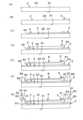
図4は、封止基板7および封止部材70の一部を破断省略した状態で図示されている。また、図5、図6、図13および図14は、封止基板7、封止部材70、第1ターミナル81および第2ターミナル82を省略した状態で図示されている。さらに、図6、図7、図8および図14は、第1金属反射膜3、透明導電膜4、全固体型EC膜5および第2金属反射膜6の膜厚を実際よりも大きな膜厚で図示されている。 FIG. 4 shows the sealing
(実施形態1の構成の説明)
図1から図12は、この発明にかかる全固体型ECミラー、車両用ミラー装置の実施形態1を示す。以下、この実施形態1にかかる全固体型ECミラー、車両用ミラー装置の構成について説明する。(Description of configuration of Embodiment 1)
1 to 12 show a first embodiment of an all-solid-state EC mirror and a vehicle mirror device according to the present invention. The configuration of the all-solid-state EC mirror and vehicle mirror device according to the first embodiment will be described below.
(車両用ミラー装置100の説明)
図1において、符号100は、この実施形態1にかかる車両用ミラー装置である。車両用ミラー装置100は、この例では、車両用アウトサイドミラー装置であって、車両用のドアミラー(以下、「ドアミラー100」と称する)である。なお、この発明においては、車両用インサイドミラー装置に使用しても良い。(Description of vehicle mirror device 100)
In FIG. 1,
ドアミラー100は、車両の左右のドアDにそれぞれ装備される。なお、図1に示されているドアミラー100は、車両の左のドアDに装備されている。ドアミラー100は、この実施形態1にかかる全固体型ECミラー1と、ミラーハウジング101と、取付部材102と、を備える。 The door mirrors 100 are installed on each of the left and right doors D of the vehicle. Note that the
ミラーハウジング101は、中空状の箱形形状をなしている。ミラーハウジング101の正面側(車両の後側)の部分には、開口部103が設けられている。 The
全固体型ECミラー1は、ミラーハウジング101の開口部103に配置されている。全固体型ECミラー1は、ミラーハウジング101に取り付けられている。 The all-solid-
ミラーハウジング101および全固体型ECミラー1は、取付部材102を介して車体であるドアDに取り付けられている。取付部材102は、ベース104と、電動格納ユニット105と、を有する。 The
ベース104は、ドアDに固定されている。電動格納ユニット105は、ベース104に固定されていて、かつ、ミラーハウジング101に取り付けられている。なお、電動格納ユニット105は、必ずしも、搭載されるものではない。すなわち、電動格納ユニット105を搭載しない車両用ミラー装置もある。 The
(全固体型ECミラー1の説明)
全固体型ECミラー1は、図1から図12に示すように、透明基板2と、透明基板2の裏面20側に積層成膜された第1金属反射膜3、透明導電膜4、全固体型EC膜5および第2金属反射膜6と、を備えるものである。(Description of all-solid-state EC mirror 1)
As shown in FIGS. 1 to 12, the all-solid-
また、全固体型ECミラー1は、封止基板7と、封止部材70と、を備えるものである。さらに、全固体型ECミラー1は、第1ターミナル81と、第2ターミナル82と、を備えるものである。 Further, the all-solid-
(透明基板2の説明)
ここで、透明基板2の裏面20は、全固体型ECミラー1のミラー面に対して、反対側の面である。すなわち、裏面20は、全固体型ECミラー1の見る側(車両の運転者の視点側)の面に対して、反対側の面である。(Description of transparent substrate 2)
Here, the
透明基板2は、この例では、ガラス板などから構成されている。透明基板2の外形は、図1に示すように、ミラーハウジング101の開口部103の内形よりも一回り小さい。透明基板2の正面21は、透明基板2の裏面20に対して反対側の面であって、全固体型ECミラー1のミラー面である。透明基板2の正面21は、凸曲面をなす。 In this example, the
なお、図3、図6、図7および図8において、透明基板2の正面21は、平面に図示されている。透明基板2の正面21は、平面などであっても良い。また、透明基板2の角部は、図3中の破線にて示すように、面取りされていても良い。 Note that in FIGS. 3, 6, 7, and 8, the
(第1金属反射膜3の説明)
第1金属反射膜3は、図5、図6および図9に示すように、透明基板2の裏面20の外周に、帯状に、成膜されている。第1金属反射膜3の一部分、この例では、下辺の中央部分には、第1金属反射膜3が成膜されていない切欠部分30が、設けられている(図4(B)を参照)。切欠部分30は、帯状の第1金属反射膜3の一部分を切り欠いて、形成されている。(Description of first metal reflective film 3)
The first metal
第1金属反射膜3は、この例では、アルミ膜から構成されている。 In this example, the first metal
(透明導電膜4の説明)
透明導電膜4は、図5、図6および図10に示すように、透明基板2および第1金属反射膜3に、透明基板2の形状よりも一回り小さい形状に、かつ、第1金属反射膜3の内周縁と透明導電膜4の外周縁とが相互に接続された状態で、成膜されている。すなわち、透明導電膜4は、透明基板2のうち第1金属反射膜3の内周縁から内側の部分(第1金属反射膜3が成膜されていない部分)、および、第1金属反射膜3のうち少なくとも内周部分に、成膜されている。透明導電膜4の外周縁のうち切欠部分30に対応する一部分には、透明導電膜4が成膜されていない凹部40が、設けられている(図4(B)を参照)。(Description of transparent conductive film 4)
As shown in FIG. 5, FIG. 6, and FIG. The film is formed such that the inner peripheral edge of the
透明導電膜4は、この例では、ITOなどから構成されている。凹部40の周方向の幅T4は、第1金属反射膜3の切欠部分30の周方向の幅T2よりも大きい。この結果、図4(B)および図5に示すように、第1金属反射膜3の切欠部分30の周方向の両端(左右両端)が、透明導電膜4の凹部40の周方向の両端(左右両端)から、突出している。なお、図10においては、第1金属反射膜3の図示を省略する。 In this example, the transparent
(全固体型EC膜5の説明)
全固体型EC膜5は、図5、図6および図11に示すように、透明基板2、第1金属反射膜3および透明導電膜4に、透明基板2の形状よりも一回り小さい形状に、成膜されている。すなわち、全固体型EC膜5は、透明基板2のうち切欠部分30と凹部40、第1金属反射膜3のうち切欠部分30の周方向の両端、および、透明導電膜4に、成膜されている。(Description of all-solid-state EC membrane 5)
As shown in FIGS. 5, 6, and 11, the all-solid-
全固体型EC膜5の外周縁の一部分、この例では、上辺の中央部分には、全固体型EC膜5が成膜されていない凹部50が、設けられている(図4(A)を参照)。全固体型EC膜5の凹部50と、第1金属反射膜3の切欠部分30および透明導電膜4の凹部40とは、透明基板2の上下両辺において、相互に、向き合っている。 A
全固体型EC膜5は、この例では、酸化発色層、固体電解質層および還元発色層の3層を順次積層した全固体積層膜で構成されている。
酸化発色層は、この例では、IrSnOx(x=1~2)などである。
固体電解質層は、この例では、TaOx(x=2~2.5)などである。
還元発色層は、この例では、WO3などである。In this example, the all-solid-
In this example, the oxidized coloring layer is made of IrSnOx (x = 1 to 2) or the like.
The solid electrolyte layer is, in this example, TaOx (x = 2 to 2.5) or the like.
The reduction color forming layer is, in this example, WO3 or the like.
全固体型EC膜5の外周縁から透明基板2の外周縁までの幅T5と、透明導電膜4の外周縁から透明基板2の外周縁までの幅T3とは、同幅寸法である。 The width T5 from the outer periphery of the all-solid-
また、凹部50における全固体型EC膜5の外周縁から透明基板2の外周縁までの幅T6は、全固体型EC膜5の外周縁から透明基板2の外周縁までの幅T5よりも大きい。この結果、凹部50の外周縁は、全固体型EC膜5の外周縁よりも内側に凹んでいる。 Further, the width T6 from the outer periphery of the all-solid-
なお、図11においては、第1金属反射膜3および透明導電膜4の図示を省略する。 Note that in FIG. 11, illustration of the first metal
(第2金属反射膜6の説明)
第2金属反射膜6は、図5、図6および図12に示すように、透明基板2、第1金属反射膜3、透明導電膜4および全固体型EC膜5に、透明基板2、透明導電膜4および全固体型EC膜5の形状よりも一回り小さい形状に、成膜されている。(Description of second metal reflective film 6)
As shown in FIG. 5, FIG. 6, and FIG. The
第2金属反射膜6の外周縁のうち切欠部分30に対応する一部分には、第2金属反射膜6が成膜されている凸部60が、設けられている(図4(B)を参照)。第2金属反射膜6の外周縁のうち全固体型EC膜5の凹部50に対応する一部分には、第2金属反射膜6が成膜されていない凹部61が、設けられている(図4(A)を参照)。 A
第2金属反射膜6は、この例では、アルミ膜から構成されている。第2金属反射膜6の外周縁から透明基板2の外周縁までの幅T8は、透明導電膜4の外周縁から透明基板2の外周縁までの幅T3および全固体型EC膜5の外周縁から透明基板2の外周縁までの幅T5よりも大きい。 In this example, the second metal
また、凸部60の周方向の幅T9は、切欠部分30の周方向の幅T2よりも小さい。この結果、図4(B)および図5に示すように、凸部60の周方向の両端(左右両端)は、切欠部分30の周方向の両端(左右両端)から、内側に位置する。 Further, the circumferential width T9 of the
さらに、凹部61における第2金属反射膜6の外周縁から透明基板2の外周縁までの幅T10は、第2金属反射膜6の外周縁から透明基板2の外周縁までの幅T8、および、全固体型EC膜5の凹部50の外周縁から透明基板2の外周縁までの幅T6、よりも大きい。この結果、凹部61の外周縁は、第2金属反射膜6の外周縁、および、全固体型EC膜5の凹部50の外周縁、よりも内側に凹んでいる。 Further, the width T10 from the outer circumferential edge of the second metal
さらにまた、凹部61の周方向の幅T11は、全固体型EC膜5の凹部50の周方向の幅T7よりも小さい。この結果、凹部61の周方向の両端(左右両端)は、全固体型EC膜5の凹部50の周方向の両端(左右両端)から内側に位置する。なお、図12においては、第1金属反射膜3、透明導電膜4および全固体型EC膜5の図示を省略する。 Furthermore, the circumferential width T11 of the
(第1金属反射膜3および第2金属反射膜6の説明)
第1金属反射膜3の内周縁と透明導電膜4の外周縁とは、前記の通り、相互に接続されている。この第1金属反射膜3および透明導電膜4の一部分は、作用電極を構成する。第2金属反射膜6は、対向電極を構成する。作用電極の第1金属反射膜3および透明導電膜4と、対向電極の第2金属反射膜6との間には、全固体型EC膜5が介在されている。この結果、第1金属反射膜3および透明導電膜4と第2金属反射膜6とは、全固体型EC膜5を介して絶縁状態ある。(Description of the first metal
As described above, the inner peripheral edge of the first metal
第1金属反射膜3は、全固体型ECミラー1の外側のミラーを構成する。第2金属反射膜6は、全固体型ECミラー1の内側のミラーを構成する。外側のミラーの第1金属反射膜3の内周部分と、内側のミラーの第2金属反射膜6の外周部分とは、非接続状態であり、かつ、透明基板2から見て隙間が無く前後に重なっている。 The first metal
外側のミラーの第1金属反射膜3の内周部分と、内側のミラーの第2金属反射膜6の外周部分とは、第2金属反射膜6の凹部61において、重なり幅R1で重なっている(図6(A)参照)。また、外側のミラーの第1金属反射膜3の内周部分と、内側のミラーの第2金属反射膜6の外周部分とは、第1金属反射膜3の切欠部分30と第2金属反射膜6の凸部60および凹部61以外において、重なり幅R2で重なっている(図6(B)参照)。 The inner peripheral part of the first metal
(封止基板7および封止部材70の説明)
透明基板2の裏面側には、封止基板7が配置されている。封止基板7は、この例では、透明基板2と同様にガラス板などから構成されている。封止基板7は、透明基板2の形状よりも一回り小さい形状をなしている。また、封止基板7の角部は、透明基板2の角部と同様に、図3中の破線にて示すように、面取りされていても良い。(Description of sealing
A sealing
透明基板2と封止基板7との間には、封止部材70が充填されている。封止部材70は、第1金属反射膜3、透明導電膜4、全固体型EC膜5、第2金属反射膜6、第1ターミナル81の一部分、および、第2ターミナル82の一部分を封止する。これにより、透明基板2、第1金属反射膜3、透明導電膜4、全固体型EC膜5、第2金属反射膜6、封止基板7、封止部材70、第1ターミナル81および第2ターミナル82が一体構造となり、全固体型ECミラー1が構成される。封止部材70は、この例では、エポキシ樹脂である。 A sealing
(スペーサ71の説明)
なお、図8(B)(C)(D)(E)に示すように、透明基板2と封止基板7との間には、スペーサ71が、介在される場合がある。スペーサ71は、透明基板2と封止基板7との間の隙間を保持する。スペーサ71は、樹脂部材などの絶縁部材から構成されている。(Description of spacer 71)
Note that, as shown in FIGS. 8(B), 8(C), 8(D), and 8(E), a
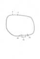
スペーサ71は、たとえば、図5中の二点鎖線の楕円にて示す2箇所に配置される。2個のスペーサ71は、全固体型ECミラー1の左右方向に配置されている。この結果、2個のスペーサ71と第1ターミナル81と第2ターミナル82は、全固体型ECミラー1の左右上下にほぼ等間隔で配置されている。 The
(第1ターミナル81、第2ターミナル82の説明)
第1金属反射膜3のうち全固体型EC膜5の凹部50および第2金属反射膜6の凹部61に対応する一部分には、第1ターミナル81が導電性ペースト(導電性接着剤、半田)80を介して接続されている(図3および図4(A)参照)。第2金属反射膜6の凸部60には、第2ターミナル82が同じく導電性ペースト80を介して接続されている(図3および図4(B)参照)。第1ターミナル81と第2ターミナル82は、全固体型ECミラー1の上下方向に配置されている。(Description of
A
第1ターミナル81、第2ターミナル82は、この例では、導電性部材(洋白など)から構成されている。 In this example, the
第1ターミナル81、第2ターミナル82は、図3および図4に示すように、側面から見て、水平部分と垂直部分とからなるL字形状をなす。第1ターミナル81、第2ターミナル82は、水平部分の接続部83と垂直部分の給電部84とから構成されている。給電部84の幅は、接続部83の幅よりも広い。すなわち、給電部84の両側が、接続部83の両側から外側に突出している。 As shown in FIGS. 3 and 4, the
接続部83は、駆動回路など(図示せず)を介して外部電源(図示せず)に接続される。給電部84は、第1ターミナル81側の作用電極(第1金属反射膜3および透明導電膜4)と第2ターミナル82側の対向電極(第2金属反射膜6)とに、それぞれ、接続されていて、作用電極と対向電極とに、それぞれ、外部電源からの電圧を印加(給電)する。すなわち、給電部84は、作用電極と対向電極とに、それぞれ、電気を供給して電流を流す。 The connecting
第1ターミナル81の一部分および第2ターミナル82の一部分は、封止部材70により封止されていて、スペーサ71と同様に、透明基板2と封止基板7との間の隙間を保持する保持部を構成する。 A portion of the
保持部は、第1当接部86と、第2当接部87と、連結部88と、から構成されている。第1当接部86は、上側の第1当接部86と下側の第1当接部86との2点で、透明基板2の裏面20に当接する。第2当接部87は、上側の第1当接部86と下側の第1当接部86との間の1箇所で、封止基板7の正面に当接する。連結部88は、上側の第1当接部86および下側の第1当接部86と第2当接部87とを相互に連結する。 The holding portion includes a
保持部の第1当接部86、第2当接部87および連結部88は、透明基板2と封止基板7との間の隙間を保持する。なお、第1当接部86は、保持部と給電部84との双方を兼用する。保持部(垂直部分の給電部84)は、透明基板2の裏面20および封止基板7の正面に対して平行な方向に、かつ、透明基板2および封止基板7の外周縁に沿って長尺形状をなす。長尺形状の保持部(垂直部分の給電部84)は、透明基板2と封止基板7との向き合う方向に弾性を有する。 The first
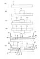
(全固体型ECミラー1の製造工程の説明)
以下、全固体型ECミラー1の製造工程について、図7および図8を参照して説明する。全固体型ECミラー1の製造工程は、前工程の成膜工程と、後工程のモジュール工程と、からなる。(Description of manufacturing process of all-solid-state EC mirror 1)
The manufacturing process of the all-solid-
製造工程1は、透明基板2をクリーニングする(図7(A)を参照)。特に、透明基板2の裏面20および正面21をクリーニングする。 In the
製造工程2は、透明基板2の裏面20の外周に、アルミ膜から構成されている第1金属反射膜3を、成膜する(図7(B)を参照)。この時、第1金属反射膜3の一部分には、切欠部分30が設けられている。 In
製造工程3は、透明基板2の裏面20および第1金属反射膜3に透明導電膜4を成膜する(図7(C)を参照)。この時、透明導電膜4の外周縁の一部分には、凹部40が設けられている。 In the
製造工程4は、透明基板2の裏面20、第1金属反射膜3および透明導電膜4に全固体型EC膜5を成膜する(図7(D)を参照)。この時、全固体型EC膜5の外周縁の一部分には、凹部50が設けられている。 In
製造工程5は、透明基板2の裏面20、第1金属反射膜3、透明導電膜4および全固体型EC膜5に第2金属反射膜6を成膜する(図7(E)を参照)。この時、第2金属反射膜6の外周縁の一部分には、凸部60と凹部61とがそれぞれ設けられている。 In the
製造工程1から製造工程5は、前工程の成膜工程である。
製造工程6は、成膜工程が完了した第1金属反射膜3と第2金属反射膜6の凸部60とに、導電性ペースト80を、それぞれ、塗布する(図7(F)を参照)。 In the
製造工程7は、第1金属反射膜3の導電性ペースト80に第1ターミナル81の給電部84を、また、第2金属反射膜6の凸部60の導電性ペースト80に第2ターミナル82の給電部84を、それぞれ、設置(載置)する(図7(G)を参照)。 In the
製造工程8は、封止基板7をクリーニングする(図8(A)を参照)。特に、封止基板7の裏面および正面をクリーニングする。 In the manufacturing process 8, the sealing
製造工程9は、封止基板7の正面にスペーサ71を設置(載置)する(図8(B)を参照)。 In the
製造工程10は、封止基板7の正面に封止部材70を塗布する(図8(C)を参照)。 In the manufacturing process 10, a sealing
製造工程8から製造工程10は、製造工程1から製造工程7と平行に行っても良い。 Manufacturing steps 8 to 10 may be performed in parallel to
製造工程11は、製造工程7において製造された透明基板2、第1金属反射膜3、透明導電膜4、全固体型EC膜5、第2金属反射膜6、導電性ペースト80、第1ターミナル81および第2ターミナル82に、製造工程10において製造された封止基板7、封止部材70およびスペーサ71を、上下逆さにして、重ね合わせる(図8(D)を参照)。 Manufacturing process 11 includes the
製造工程12は、製造工程7において製造された透明基板2、第1金属反射膜3、透明導電膜4、全固体型EC膜5、第2金属反射膜6、導電性ペースト80、第1ターミナル81および第2ターミナル82と、製造工程10において製造された封止基板7、封止部材70およびスペーサ71とを、封止部材70の高温硬化により、一体にする(図8(E)を参照)。この時、第1金属反射膜3、透明導電膜4、全固体型EC膜5、第2金属反射膜6、第1ターミナル81の一部分、および、第2ターミナル82の一部分は、封止部材70により封止されている。また、透明基板2と封止基板7との間の隙間は、第1ターミナル81のおよび第2ターミナル82により、保持されている。 The manufacturing process 12 includes the
この製造工程1から製造工程12までの工程により、全固体型ECミラー1が製造される。 The all-solid-
(実施形態1の作用の説明)
この実施形態1にかかる全固体型ECミラー1、車両用ミラー装置100は、以上のごとき構成からなり、以下、その作用について説明する。(Explanation of action of Embodiment 1)
The all-solid-
全固体型ECミラー1のミラー面は、正面側(車両の後側)に向いていて、車両の後側の情報を写す。運転者は、全固体型ECミラー1のミラー面に写し出された車両の後側の情報を視認する。 The mirror surface of the all-solid-
この時、全固体型ECミラー1のミラー面は、第1金属反射膜3の外側のミラーと、第2金属反射膜6の内側のミラーとにより、全固体型ECミラー1の全面がミラー面となる。 At this time, the entire surface of the all-solid-
第1ターミナル81および第2ターミナル82を介して、作用電極(第1金属反射膜3および透明導電膜4)と対向電極(第2金属反射膜6)とに、それぞれ、電圧を印加(給電)する。 A voltage is applied (power supply) to the working electrode (first metal
すると、全固体型EC膜5の光透過率が変化する。これにより、透明基板2の正面21側、すなわち、見る側(車両の運転者の視点側)から、透明基板2、透明導電膜4および全固体型EC膜5を透過して見た第2金属反射膜6の反射率が変化する。 Then, the light transmittance of the all-solid-
昼モードの高反射率のミラー面と、夜モードの低反射率のミラー面とが得られる。この時、反射率が変化するのは、全固体型ECミラー1のミラー面のうち、第2金属反射膜6に対応する内側のミラーである。外側のミラーの反射率は、変化しない。 A mirror surface with high reflectance in daytime mode and a mirror surface with low reflectance in night mode are obtained. At this time, the reflectance changes on the inner mirror corresponding to the second metal
(実施形態1の効果の説明)
この実施形態1にかかる全固体型ECミラー1、車両用ミラー装置100は、以上のごとき構成、作用からなり、以下、その効果について説明する。(Explanation of effects of Embodiment 1)
The all-solid-
この実施形態1にかかる全固体型ECミラー1、車両用ミラー装置100は、透明基板2の外周に成膜された第1金属反射膜3により外側のミラーを構成し、透明基板2の内周に成膜された第2金属反射膜6により内側のミラーを構成するものである。この結果、この実施形態1にかかる全固体型ECミラー1、車両用ミラー装置100は、前記の特許文献1の固体型ECミラーと比較して、量産性があり、また、リーク電流を防止できる。 In the all-solid-
この実施形態1にかかる全固体型ECミラー1、車両用ミラー装置100は、全面のミラー面が得られるので、通電性クリップを備えたエレクトロクロミック素子(特開昭62-270925号公報参照)と比較して、外周にクリップが見えなくなり、外観上の見栄えが向上(改善)される。 The all-solid-
しかも、この実施形態1にかかる全固体型ECミラー1、車両用ミラー装置100は、前記の通電性クリップを備えたエレクトロクロミック素子と比較して、外周のクリップを隠すためのベゼルが不要となる。この結果、この実施形態1にかかる全固体型ECミラー1、車両用ミラー装置100は、ミラー面領域が拡大し、法規上、必要なミラー面領域を縮小することができ、その分、ミラーおよび装置の小型化および軽量化を図ることができる。 Furthermore, the all-solid-
この実施形態1にかかる全固体型ECミラー1、車両用ミラー装置100は、外側のミラーの第1金属反射膜3の内周部分と内側のミラーの第2金属反射膜6の外周部分とが非接続状態であり、かつ、透明基板2から見て隙間が無く前後に重なっているものである。この結果、この実施形態1にかかる全固体型ECミラー1、車両用ミラー装置100は、全面において切れ目がほとんど無い、ミラー面(鏡面)が得られる。 In the all-solid-
この実施形態1にかかる全固体型ECミラー1、車両用ミラー装置100は、第1金属反射膜3のうち全固体型EC膜5の凹部50および第2金属反射膜6の凹部61に対応する一部分に第1ターミナル81が接続されていて、第2金属反射膜6の凸部60に第2ターミナル82が接続されている。この結果、この実施形態1にかかる全固体型ECミラー1、車両用ミラー装置100は、作用電極の第1金属反射膜3と対向電極の第2金属反射膜6とに、それぞれ、電圧を確実に印加(給電)することができる。 The all-solid-
この実施形態1にかかる全固体型ECミラー1、車両用ミラー装置100は、透明基板2と封止基板7との間に封止部材70を充填し、かつ、その封止部材70により、第1金属反射膜3、透明導電膜4、全固体型EC膜5、第2金属反射膜6、第1ターミナル81の一部分、および、第2ターミナル82の一部分を封止するものである。この結果、この実施形態1にかかる全固体型ECミラー1、車両用ミラー装置100は、ガルバニック腐食を確実に防止することができる。これにより、この実施形態1にかかる全固体型ECミラー1、車両用ミラー装置100は、アウターミラー(車両用アウトサイドミラー装置)として、使用することができる。 The all-solid-
この実施形態1にかかる全固体型ECミラー1、車両用ミラー装置100は、第1ターミナル81の保持部および第2ターミナル82の保持部が透明基板2と封止基板7との間の隙間を保持するものである。この結果、この実施形態1にかかる全固体型ECミラー1、車両用ミラー装置100は、封止部材70のオーバーフローやアンダーフィルによる不良を防止できる。 In the all-solid-
(実施形態2の構成、作用、効果の説明)
図13および図14は、この発明にかかる全固体型ECミラー1A、車両用ミラー装置の実施形態2を示す。以下、この実施形態2にかかる全固体型ECミラー1A、車両用ミラー装置の構成、作用、効果について説明する。図中、図1~図12と同符号は、同一物を示す。(Explanation of configuration, action, and effect of Embodiment 2)
13 and 14 show a second embodiment of an all-solid-
この実施形態2にかかる全固体型ECミラー1A、車両用ミラー装置100は、発光表示部を有するものである。この発光表示部は、ブラインドスポットワーニング(BSW)装置における一構成部である。 The all-solid-
ブラインドスポットワーニング(BSW)装置は、車両の走行中において、車両の斜め後方の運転者の死角に他の車両が所定の距離に近づくと、レーダなどのセンサが接近する他の車両を検出して、制御部が発光表示部を発光させて、運転者に他の車両の接近を知らせる装置である。 A blind spot warning (BSW) device detects when another vehicle approaches a predetermined distance from the driver's blind spot diagonally behind the vehicle while the vehicle is running. In this device, a control unit causes a light emitting display unit to emit light to notify the driver of the approach of another vehicle.
この実施形態2にかかる全固体型ECミラー1A、車両用ミラー装置100は、発光表示部に、光源9と、マーク90と、を有する。 The all-solid-
マーク90は、全固体型ECミラー1Aの透明基板2であって、全固体型ECミラー1Aの第1金属反射膜3、全固体型EC膜5および第2金属反射膜6が成膜されていない一部分に施されている。マーク90は、この例では、エッチングやブラストなどにより施されている。マーク90は、光Lを透過させる機能を有する。なお、マーク90の意匠は、特に、限定しない。 The
光源9は、全固体型ECミラー1Aの裏側に配置されている。光源9は、たとえば、LEDもしくはOLED(有機EL)などの自発光半導体型発光素子(半導体発光素子)タイプの光源を使用する。なお、光源9は、LEDなどの自発光型光源以外の光源(たとえば、導光板を用いた間接光源)であっても良い。 The
ここで、車両の走行中において、ブラインドスポットワーニング(BSW)装置のセンサが接近する他の車両を検出すると、制御部が光源9を点灯させる。光源9から放射された光Lは、マーク90が施されている全固体型ECミラー1Aの透明基板2の一部分を透過する。 Here, when the sensor of the blind spot warning (BSW) device detects another approaching vehicle while the vehicle is running, the control section turns on the
これにより、全固体型ECミラー1Aの透明基板2の一部分に、マーク90が発光表示される。この結果、運転者が、発光表示されているマーク90を視認して、他の車両の接近を認識して、安全運転に心掛けることができる。 As a result, the
この実施形態2にかかる全固体型ECミラー1A、車両用ミラー装置100は、以上のごとき構成からなるので、前記の実施形態1にかかる全固体型ECミラー1、車両用ミラー装置100と同様の作用、効果を達成することができる。 Since the all-solid-
(実施形態1、2以外の例の説明)
なお、前記の実施形態1、2にかかる全固体型ECミラー1、1A、車両用ミラー装置100は、車両用アウトサイドミラー装置について説明するものである。しかしながら、この発明においては、前記の通り、車両用インサイドミラー装置に使用しても良い。また、この発明においては、車両用のミラー装置以外のミラー装置にも使用することができる。(Explanation of examples other than
Note that the all-solid-state EC mirrors 1 and 1A and the
また、この発明は、前記の実施形態1、2により限定されるものではない。 Further, the present invention is not limited to the first and second embodiments described above.
1、1A 全固体型ECミラー
2 透明基板
20 裏面
21 正面
3 第1金属反射膜
30 切欠部分
4 透明導電膜
40 凹部
5 全固体型EC膜
50 凹部
6 第2金属反射膜
60 凸部
61 凹部
7 封止基板
70 封止部材
71 スペーサ
80 導電性ペースト(導電性接着剤、半田)
81 第1ターミナル
82 第2ターミナル
83 接続部
84 給電部
86 第1当接部
87 第2当接部
88 連結部
9 光源
90 マーク
100 ドアミラー(車両用ミラー装置)
101 ミラーハウジング
102 取付部材
103 開口部
104 ベース
105 電動格納ユニット
D ドア(車体)
L 光
R1 重なり幅
R2 重なり幅
T1 幅
T2 幅
T3 幅
T4 幅
T5 幅
T6 幅
T7 幅
T8 幅
T9 幅
T10 幅
T11 幅1, 1A All-solid-
81
L light R1 Overlapping width R2 Overlapping width T1 Width T2 Width T3 Width T4 Width T5 Width T6 Width T7 Width T8 Width T9 Width T10 Width T11 Width
Claims (7)
Translated fromJapanese前記透明基板の裏面側に積層成膜された第1金属反射膜、透明導電膜、全固体型EC膜、および、第2金属反射膜と、
を備え、
前記第1金属反射膜は、前記透明基板の外周に、帯状に、成膜されていて、
前記第1金属反射膜の一部分には、前記第1金属反射膜が成膜されていない切欠部分が、設けられていて、
前記透明導電膜は、前記透明基板および前記第1金属反射膜に、前記透明基板の形状よりも一回り小さい形状に、かつ、前記第1金属反射膜の内周縁と前記透明導電膜の外周縁とが相互に接続された状態で、成膜されていて、
前記透明導電膜の外周縁のうち前記切欠部分に対応する一部分には、前記透明導電膜が成膜されていない凹部が、設けられていて、
前記全固体型EC膜は、前記透明基板、前記第1金属反射膜および前記透明導電膜に、前記透明基板の形状よりも一回り小さい形状に、成膜されていて、
前記全固体型EC膜の外周縁の一部分には、前記全固体型EC膜が成膜されていない凹部が、設けられていて、
前記第2金属反射膜は、前記透明基板、前記第1金属反射膜、前記透明導電膜および前記全固体型EC膜に、前記透明基板、前記透明導電膜および前記全固体型EC膜の形状よりも一回り小さい形状に、成膜されていて、
前記第2金属反射膜の外周縁のうち前記切欠部分に対応する一部分には、前記第2金属反射膜が成膜されている凸部が、設けられていて、
前記第2金属反射膜の外周縁のうち前記全固体型EC膜の前記凹部に対応する一部分には、前記第2金属反射膜が成膜されていない凹部が、設けられていて、
前記第1金属反射膜および前記透明導電膜は、作用電極を構成し、
前記第2金属反射膜は、対向電極を構成し、
前記作用電極の前記第1金属反射膜および前記透明導電膜と、前記対向電極の前記第2金属反射膜との間には、前記全固体型EC膜が介在されている、
ことを特徴とする全固体型ECミラー。a transparent substrate;
A first metal reflective film, a transparent conductive film, an all-solid-state EC film, and a second metal reflective film, which are laminated on the back side of the transparent substrate;
Equipped with
The first metal reflective film is formed in a band shape around the outer periphery of the transparent substrate,
A portion of the first metal reflective film is provided with a cutout portion where the first metal reflective film is not formed,
The transparent conductive film is formed on the transparent substrate and the first metal reflective film, and has a shape that is one size smaller than the shape of the transparent substrate, and has an inner peripheral edge of the first metal reflective film and an outer peripheral edge of the transparent conductive film. are formed in a state where they are interconnected,
A recessed portion on which the transparent conductive film is not formed is provided in a portion of the outer peripheral edge of the transparent conductive film corresponding to the cutout portion,
The all-solid-state EC film is formed on the transparent substrate, the first metal reflective film, and the transparent conductive film in a shape that is one size smaller than the shape of the transparent substrate,
A recessed portion where the all-solid-state EC film is not formed is provided in a part of the outer peripheral edge of the all-solid-state EC film,
The second metal reflective film is formed on the transparent substrate, the first metal reflective film, the transparent conductive film, and the all-solid-state EC film, depending on the shape of the transparent substrate, the transparent conductive film, and the all-solid-state EC film. The film is formed into a slightly smaller shape,
A convex portion on which the second metal reflective film is formed is provided in a portion of the outer peripheral edge of the second metal reflective film corresponding to the cutout portion,
A recess on which the second metal reflective film is not formed is provided in a portion of the outer peripheral edge of the second metal reflective film corresponding to the recess of the all-solid-state EC film,
The first metal reflective film and the transparent conductive film constitute a working electrode,
The second metal reflective film constitutes a counter electrode,
The all-solid-state EC film is interposed between the first metal reflective film and the transparent conductive film of the working electrode and the second metal reflective film of the counter electrode.
This is an all-solid-state EC mirror.
前記第2金属反射膜は、内側のミラーを構成し、
前記外側のミラーの前記第1金属反射膜の内周部分と、前記内側のミラーの前記第2金属反射膜の外周部分とは、非接続状態であり、かつ、前記透明基板から見て重なっている、
ことを特徴とする請求項1に記載の全固体型ECミラー。the first metal reflective film constitutes an outer mirror;
the second metal reflective film constitutes an inner mirror;
The inner peripheral part of the first metal reflective film of the outer mirror and the outer peripheral part of the second metal reflective film of the inner mirror are not connected and overlap when viewed from the transparent substrate. There is,
The all-solid-state EC mirror according to claim 1, characterized in that:
前記第2金属反射膜の前記凸部には、第2ターミナルが接続されている、
ことを特徴とする請求項1または2に記載の全固体型ECミラー。A first terminal is connected to a portion of the first metal reflective film corresponding to the concave portion of the all-solid-state EC film and the concave portion of the second metal reflective film,
A second terminal is connected to the convex portion of the second metal reflective film,
The all-solid-state EC mirror according to claim 1 or 2, characterized in that:
前記透明基板と前記封止基板との間に充填されていて、前記第1金属反射膜、前記透明導電膜、前記全固体型EC膜、前記第2金属反射膜、前記第1ターミナルの一部分、および、前記第2ターミナルの一部分を封止する封止部材と、
を備える、
ことを特徴とする請求項3に記載の全固体型ECミラー。a sealing substrate disposed on the back side of the transparent substrate;
Filled between the transparent substrate and the sealing substrate, the first metal reflective film, the transparent conductive film, the all-solid EC film, the second metal reflective film, and a portion of the first terminal; and a sealing member that seals a portion of the second terminal;
Equipped with
The all-solid-state EC mirror according to claim 3, characterized in that:
ことを特徴とする請求項4に記載の全固体型ECミラー。A holding portion for holding a gap between the transparent substrate and the sealing substrate is provided in a portion of the first terminal and a portion of the second terminal, respectively.
The all-solid-state EC mirror according to claim 4.
前記全固体型ECミラーが取り付けられているミラーハウジングと、
前記ミラーハウジングを車体に取り付ける取付部材と、
を備える、
ことを特徴とする車両用ミラー装置。The all-solid-state EC mirror according to any one of claims 1 to 5 above,
a mirror housing to which the all-solid-state EC mirror is attached;
a mounting member for attaching the mirror housing to the vehicle body;
Equipped with
A vehicle mirror device characterized by:
前記全固体型ECミラーにおいて、
第1金属反射膜のうち、全固体型EC膜が成膜されていない一部分には、マークが施されていて、
前記マークは、前記光源からの光を、透明基板側に透過させる、
ことを特徴とする請求項6に記載の車両用ミラー装置。comprising a light source disposed on the back side of the all-solid-state EC mirror,
In the all-solid-state EC mirror,
A mark is applied to a portion of the first metal reflective film where the all-solid-state EC film is not formed.
The mark transmits light from the light source to the transparent substrate side.
The vehicle mirror device according to claim 6, characterized in that:
Priority Applications (1)
| Application Number | Priority Date | Filing Date | Title |
|---|---|---|---|
| JP2020094208AJP7373463B2 (en) | 2020-05-29 | 2020-05-29 | All-solid-state EC mirror, vehicle mirror device |
Applications Claiming Priority (1)
| Application Number | Priority Date | Filing Date | Title |
|---|---|---|---|
| JP2020094208AJP7373463B2 (en) | 2020-05-29 | 2020-05-29 | All-solid-state EC mirror, vehicle mirror device |
Publications (2)
| Publication Number | Publication Date |
|---|---|
| JP2021189301A JP2021189301A (en) | 2021-12-13 |
| JP7373463B2true JP7373463B2 (en) | 2023-11-02 |
Family
ID=78849669
Family Applications (1)
| Application Number | Title | Priority Date | Filing Date |
|---|---|---|---|
| JP2020094208AActiveJP7373463B2 (en) | 2020-05-29 | 2020-05-29 | All-solid-state EC mirror, vehicle mirror device |
Country Status (1)
| Country | Link |
|---|---|
| JP (1) | JP7373463B2 (en) |
Citations (7)
| Publication number | Priority date | Publication date | Assignee | Title |
|---|---|---|---|---|
| US5066112A (en) | 1989-12-21 | 1991-11-19 | Donnelly Corporation | Perimeter coated, electro-optic mirror |
| JP2002528745A (en) | 1998-10-20 | 2002-09-03 | ジェンテクス・コーポレーション | Electrochromic mirror with third surface reflector |
| WO2003032068A1 (en) | 2001-10-05 | 2003-04-17 | Murakami Corporation | Fully solid electrochromic element |
| US20080212189A1 (en) | 2005-05-16 | 2008-09-04 | Donnelly Corporation | Vehicle Mirror Assembly With Indicia At Reflective Element |
| JP2014019241A (en) | 2012-07-17 | 2014-02-03 | Honda Lock Mfg Co Ltd | Glare-proof mirror, vehicle, and method for manufacturing glare-proof mirror |
| JP2016035521A (en) | 2014-08-04 | 2016-03-17 | 株式会社村上開明堂 | Solid type ec mirror for vehicle |
| CN107632479A (en) | 2017-11-07 | 2018-01-26 | 宁波祢若电子科技有限公司 | A kind of modified electrochromism automobile rear view mirror lens |
Family Cites Families (1)
| Publication number | Priority date | Publication date | Assignee | Title |
|---|---|---|---|---|
| JPS63306429A (en)* | 1987-06-09 | 1988-12-14 | Ichikoh Ind Ltd | Manufacturing method of EC anti-glare mirror for automobiles |
- 2020
- 2020-05-29JPJP2020094208Apatent/JP7373463B2/enactiveActive
Patent Citations (7)
| Publication number | Priority date | Publication date | Assignee | Title |
|---|---|---|---|---|
| US5066112A (en) | 1989-12-21 | 1991-11-19 | Donnelly Corporation | Perimeter coated, electro-optic mirror |
| JP2002528745A (en) | 1998-10-20 | 2002-09-03 | ジェンテクス・コーポレーション | Electrochromic mirror with third surface reflector |
| WO2003032068A1 (en) | 2001-10-05 | 2003-04-17 | Murakami Corporation | Fully solid electrochromic element |
| US20080212189A1 (en) | 2005-05-16 | 2008-09-04 | Donnelly Corporation | Vehicle Mirror Assembly With Indicia At Reflective Element |
| JP2014019241A (en) | 2012-07-17 | 2014-02-03 | Honda Lock Mfg Co Ltd | Glare-proof mirror, vehicle, and method for manufacturing glare-proof mirror |
| JP2016035521A (en) | 2014-08-04 | 2016-03-17 | 株式会社村上開明堂 | Solid type ec mirror for vehicle |
| CN107632479A (en) | 2017-11-07 | 2018-01-26 | 宁波祢若电子科技有限公司 | A kind of modified electrochromism automobile rear view mirror lens |
Also Published As
| Publication number | Publication date |
|---|---|
| JP2021189301A (en) | 2021-12-13 |
Similar Documents
| Publication | Publication Date | Title |
|---|---|---|
| US7417781B2 (en) | Electrochromic rearview mirror incorporating a third surface reflector | |
| EP3285114A1 (en) | Rear-view mirror and driving auxiliary apparatus | |
| US8888341B2 (en) | Vehicle door mirror | |
| US20190134954A1 (en) | Luminous signaling glazing, vehicle incorporating same and manufacture | |
| CN104620173B (en) | Electrochromic mirror | |
| US20020080463A1 (en) | Electrochromic rearview mirror incorporating a third surface partially transmissive reflector | |
| EP3694000A1 (en) | Electronic panel and electronic device including same | |
| JP2014008877A (en) | Vehicular rear panel | |
| JP2019522613A (en) | Vehicle windshield for head-up display and vehicle incorporating the same and manufacture of said windshield | |
| WO2016021302A1 (en) | Vehicular solid-state type ec mirror | |
| JP7129651B2 (en) | input device | |
| JP2016141573A (en) | Double glazing and optical device | |
| US6366391B1 (en) | Electrochrome cell | |
| US20150274064A1 (en) | Vehicle lamp | |
| WO2013132904A1 (en) | Electronic device and spacer with metal thin film | |
| JP7373463B2 (en) | All-solid-state EC mirror, vehicle mirror device | |
| EP3614042B1 (en) | Vehicular lamp | |
| JP7453854B2 (en) | All-solid-state EC mirror, vehicle mirror device | |
| CN112230486B (en) | Electrochromic device and electronic terminal comprising same | |
| JP2022167049A (en) | All-solid-state EC mirror, all-solid-state EC mirror unit, vehicle mirror device | |
| JP7533452B2 (en) | Light-adjusting sheet and light-adjusting device | |
| WO2017187913A1 (en) | Light emitting system | |
| JP2008015427A (en) | Image display medium | |
| JP3924103B2 (en) | Electrochromic mirror | |
| CN221039483U (en) | Coating film layer structure of automobile outer rearview mirror lens |
Legal Events
| Date | Code | Title | Description |
|---|---|---|---|
| A621 | Written request for application examination | Free format text:JAPANESE INTERMEDIATE CODE: A621 Effective date:20230308 | |
| A711 | Notification of change in applicant | Free format text:JAPANESE INTERMEDIATE CODE: A712 Effective date:20230317 | |
| RD04 | Notification of resignation of power of attorney | Free format text:JAPANESE INTERMEDIATE CODE: A7424 Effective date:20230531 | |
| RD02 | Notification of acceptance of power of attorney | Free format text:JAPANESE INTERMEDIATE CODE: A7422 Effective date:20230630 | |
| A977 | Report on retrieval | Free format text:JAPANESE INTERMEDIATE CODE: A971007 Effective date:20230927 | |
| TRDD | Decision of grant or rejection written | ||
| A01 | Written decision to grant a patent or to grant a registration (utility model) | Free format text:JAPANESE INTERMEDIATE CODE: A01 Effective date:20231017 | |
| A61 | First payment of annual fees (during grant procedure) | Free format text:JAPANESE INTERMEDIATE CODE: A61 Effective date:20231023 | |
| R150 | Certificate of patent or registration of utility model | Ref document number:7373463 Country of ref document:JP Free format text:JAPANESE INTERMEDIATE CODE: R150 |