JP7373336B2 - Circuit board and imaging device - Google Patents
Circuit board and imaging deviceDownload PDFInfo
- Publication number
- JP7373336B2 JP7373336B2JP2019171032AJP2019171032AJP7373336B2JP 7373336 B2JP7373336 B2JP 7373336B2JP 2019171032 AJP2019171032 AJP 2019171032AJP 2019171032 AJP2019171032 AJP 2019171032AJP 7373336 B2JP7373336 B2JP 7373336B2
- Authority
- JP
- Japan
- Prior art keywords
- circuit board
- base material
- surface contact
- area
- pattern
- Prior art date
- Legal status (The legal status is an assumption and is not a legal conclusion. Google has not performed a legal analysis and makes no representation as to the accuracy of the status listed.)
- Active
Links
Images


Landscapes
- Structure Of Printed Boards (AREA)
- Photometry And Measurement Of Optical Pulse Characteristics (AREA)
- Solid State Image Pick-Up Elements (AREA)
- Transforming Light Signals Into Electric Signals (AREA)
- Studio Devices (AREA)
- Non-Metallic Protective Coatings For Printed Circuits (AREA)
- Shielding Devices Or Components To Electric Or Magnetic Fields (AREA)
Description
Translated fromJapanese本発明の一態様は、センサが配置される回路基板に関する。 One aspect of the present invention relates to a circuit board on which a sensor is arranged.
ベアチップ状半導体装置を接着剤でダイパッド上に実装する半導体装置の実装方法がある。このような半導体装置の実装方法は、たとえば特許文献1などに開示されている。 There is a semiconductor device mounting method in which a bare chip semiconductor device is mounted on a die pad using an adhesive. Such a semiconductor device mounting method is disclosed in, for example,
たとえば、撮像素子などのセンサが配置された回路基板をカメラのケースに固定する場合、回路基板とケースとが面接触することによって、ケースに対するセンサの位置精度が確保される構成にすることがある。 For example, when fixing a circuit board on which a sensor such as an image sensor is arranged to a camera case, the circuit board and the case may come into surface contact to ensure the positional accuracy of the sensor relative to the case. .
BGA(Ball Grid Array)などによってセンサと回路基板とが電気的に接続にされる場合、アンダーフィル接着剤などの補強材をセンサと回路基板との間に流し込むことによって、センサと回路基板との物理的な接続が補強されることがある。しかしながら、補強材がセンサの周囲にも流れ出して固化し、回路基板上のケースと面接触する部分に凹凸が形成されると、当該部分の面精度が劣化し、ケースに対するセンサの位置精度を確保することが困難となることがある。 When the sensor and circuit board are electrically connected by BGA (Ball Grid Array) etc., the connection between the sensor and the circuit board can be improved by pouring reinforcing material such as underfill adhesive between the sensor and the circuit board. Physical connections may be reinforced. However, if the reinforcing material flows around the sensor and solidifies, and unevenness is formed on the part of the circuit board that makes surface contact with the case, the surface accuracy of that part deteriorates, ensuring the positional accuracy of the sensor relative to the case. It may be difficult to do so.
ところで、特許文献1に記載の半導体装置の実装方法のように、センサの周囲に溝を形成して補強材の流れ出しを抑制することがある。しかしながら、当該溝には銅箔のパターンが形成されないため、基板の内側の層に形成された配線から発せられる電波を遮蔽することができなくなることがある。また、溝を避けるように銅箔のパターンが配置されることによって、パターンの隙間から電波を放射してしまうことがある。回路基板とケースとが接触する部分に補強材が流れ出すことを抑制しながら、電波対策を行うことが可能な技術が求められる。 Incidentally, as in the semiconductor device mounting method described in
本発明は、上記の課題などを解決するために次のような手段を採る。なお、以下の説明において、発明の理解を容易にするために図面中の符号等を括弧書きで付記するが、本発明の各構成要素はこれらの付記したものに限定されるものではなく、当業者が技術的に理解しうる範囲にまで広く解釈されるべきものである。 The present invention takes the following measures to solve the above problems. In the following description, reference numerals in the drawings are added in parentheses to facilitate understanding of the invention, but the constituent elements of the present invention are not limited to those added. It should be interpreted broadly to the extent that a trader can technically understand it.
本発明の一の手段は、
他の部材(42)に固定される回路基板(1)であって、
回路素子(43)が配置された基材(11)と、
前記基材上に導電体で形成されたパターン(12)と、
前記基材または前記パターン上に形成された絶縁層(13)と、
前記基材、前記パターンまたは前記絶縁層上に形成された、前記回路素子の固定を補強する補強材と、を備え、
前記基材は、平面視において、
前記回路素子が配置される素子配置領域(21)と、
前記他の部材と面接触する面接触領域(22)と、
前記素子配置領域と前記面接触領域との間に位置し、前記絶縁層が形成されない非形成領域と(23、33)、を含む、
回路基板である。One means of the present invention is
A circuit board (1) fixed to another member (42),
a base material (11) on which a circuit element (43) is arranged;
a pattern (12) formed of a conductor on the base material;
an insulating layer (13) formed on the base material or the pattern;
a reinforcing material formed on the base material, the pattern, or the insulating layer to reinforce fixation of the circuit element,
In plan view, the base material has the following features:
an element placement area (21) in which the circuit element is placed;
a surface contact area (22) that makes surface contact with the other member;
a non-formation region (23, 33) located between the element arrangement region and the surface contact region, where the insulating layer is not formed;
It is a circuit board.
上記構成の回路基板によれば、周辺に対して凹んだ非形成領域が素子配置領域と面接触領域との間に位置することで、素子配置領域から面接触領域への補強材の流れ出しを抑制することができる。また、非形成領域には、絶縁層が形成されないだけであるので、パターンを形成することができる。これにより、電波の遮蔽、及び電波の放射抑制といった電波対策を行うことができる。 According to the circuit board having the above configuration, the non-forming area recessed with respect to the periphery is located between the element placement area and the surface contact area, thereby suppressing the reinforcing material from flowing out from the element placement area to the surface contact area. can do. Furthermore, since no insulating layer is formed in the non-forming region, a pattern can be formed thereon. This makes it possible to take measures against radio waves, such as shielding radio waves and suppressing radio wave radiation.
上記回路基板において、好ましくは、
前記非形成領域には、接地された前記パターン(24)が形成される。In the above circuit board, preferably,
The grounded pattern (24) is formed in the non-formation area.
上記構成の回路基板によれば、電波の遮蔽、及び電波の放射抑制に有効な、接地されたパターンを非形成領域に形成することで、電波対策を効果的に行うことができる。 According to the circuit board having the above configuration, countermeasures against radio waves can be effectively taken by forming a grounded pattern in the non-formation area, which is effective for shielding radio waves and suppressing radio wave radiation.
上記回路基板において、好ましくは、
前記回路素子は、撮像素子である。In the above circuit board, preferably,
The circuit element is an image sensor.
上記構成の回路基板によれば、補強材の流れ込みによる面接触領域の面精度の悪化を抑制することができるので、ケースに対する位置精度が求められる撮像素子を精度よく配置することができる。 According to the circuit board having the above configuration, it is possible to suppress the deterioration of the surface accuracy of the surface contact area due to the reinforcing material flowing in, so that it is possible to accurately arrange the image sensor, which requires positional accuracy with respect to the case.
上記回路基板において、好ましくは、
前記基材は、千鳥状に配置された複数の前記非形成領域(23)を含む。In the above circuit board, preferably,
The base material includes a plurality of the non-forming regions (23) arranged in a staggered manner.
上記構成の回路基板によれば、パターンの露出を細分することができるので、異なる電位のパターンに金属部材が当接し、パターン間が短絡することを抑制することができる。 According to the circuit board having the above configuration, since the exposure of the pattern can be subdivided, it is possible to suppress the metal member from coming into contact with patterns of different potentials and causing a short circuit between the patterns.
上記回路基板において、好ましくは、
前記基材は、略直線状の前記非形成領域(33)を含む。In the above circuit board, preferably,
The base material includes the non-formation region (33) that is substantially linear.
上記構成の回路基板によれば、非形成領域を直線状に形成することで、素子配置領域から面接触領域への補強材の流れ出しを、連続する非形成領域によって効果的に抑制することができる。また、非形成領域を簡易に形成することができる。 According to the circuit board having the above configuration, by forming the non-forming region in a linear shape, it is possible to effectively suppress the reinforcing material from flowing out from the element arrangement region to the surface contact region by the continuous non-forming region. . Further, a non-forming region can be easily formed.
上記の回路基板は、車載カメラ、デジタルカメラ、スマートフォン及びタブレット機器などの撮像装置に好適に適用される。 The above circuit board is suitably applied to imaging devices such as in-vehicle cameras, digital cameras, smartphones, and tablet devices.
上記構成の撮像装置によれば、段差状に凹んだ非形成領域が素子配置領域と面接触領域との間に位置することで、素子配置領域から面接触領域への補強材の流れ出しを抑制することができる。これにより、面接触領域の面精度を確保することができるので、レンズに対する位置精度が求められる撮像素子を精度よく配置することができる。また、非形成領域には、絶縁層が形成されないだけであるので、パターンを形成することができる。これにより、電波の遮蔽、及び電波の放射抑制といった電波対策を行うことができる。 According to the imaging device having the above configuration, the non-formation region recessed in a stepped shape is located between the element arrangement region and the surface contact region, thereby suppressing the reinforcing material from flowing out from the element arrangement region to the surface contact region. be able to. Thereby, the surface accuracy of the surface contact area can be ensured, so it is possible to accurately arrange the image sensor, which requires positional accuracy with respect to the lens. Furthermore, since no insulating layer is formed in the non-forming region, a pattern can be formed thereon. This makes it possible to take measures against radio waves, such as shielding radio waves and suppressing radio wave radiation.
本発明の回路基板は、基材が、平面視において、回路素子が配置される素子配置領域と、ケースと面接触する面接触領域と、素子配置領域と面接触領域との間に位置し、絶縁層が形成されない非形成領域と、を含むように構成されている点を特徴のひとつとする。 In the circuit board of the present invention, the base material is located between, in plan view, an element placement area where the circuit elements are placed, a surface contact area that makes surface contact with the case, and the element placement area and the surface contact area, One of the features is that it is configured to include a non-forming region where an insulating layer is not formed.
本発明に係る実施形態について、以下の構成に従って説明する。ただし、以下で説明する実施形態はあくまで本発明の一例にすぎず、本発明の技術的範囲を限定的に解釈させるものではない。なお、各図面において、同一の構成要素には同一の符号を付しており、その説明を省略する場合がある。
1.実施形態
2.変形例
3.補足事項Embodiments according to the present invention will be described according to the following configuration. However, the embodiments described below are merely examples of the present invention, and the technical scope of the present invention should not be construed as limiting. In addition, in each drawing, the same components are given the same reference numerals, and their explanations may be omitted.
1. Embodiment 2. Modification example 3. Additional information
<1.実施形態>
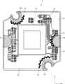
本発明の実施形態について、図面を参照しながら説明する。図1は、本実施形態の撮像装置の断面図である。図2は、本実施形態の回路基板の平面図である。図3は、本実施形態の回路基板の断面図である。図1~図3には、x軸、y軸およびz軸を示している。回路基板1の表面に垂直な方向であって、基材11から見て撮像素子43へ向いている軸を「z軸」と定義する。z軸に垂直な軸であって、回路基板1の一辺と平行な軸を「x軸」と定義する。また、x軸およびz軸の両方に垂直な軸を「y軸」と定義する。ここでは、x軸、y軸およびz軸は、右手系の3次元の直交座標を形成する。以下、z軸の矢印方向をz軸+側、矢印とは逆方向をz軸-側と呼ぶことがあり、その他の軸についても同様である。なお、z軸+側及びz軸-側を、それぞれ「フロント側」及び「リア側」と呼ぶこともある。<1. Embodiment>
Embodiments of the present invention will be described with reference to the drawings. FIG. 1 is a cross-sectional view of the imaging device of this embodiment. FIG. 2 is a plan view of the circuit board of this embodiment. FIG. 3 is a cross-sectional view of the circuit board of this embodiment. In FIGS. 1 to 3, the x-axis, y-axis, and z-axis are shown. The axis perpendicular to the surface of the
<撮像装置41>
図1~図3に示されるように、本実施形態の撮像装置41は、回路基板1、レンズ鏡筒42、撮像素子43及びレンズ44を含んで構成される。レンズ鏡筒42は、略円筒形状の部材である。回路基板1は、略矩形の断面を有する板状の部材である。回路基板1のフロント側の表面には、撮像素子43が配置される。レンズ44は、レンズ鏡筒42の内側に固定(保持)され、撮像素子43と対向する。レンズ鏡筒42は、本発明でいう「ケース」及び「他の部材」の一具体例である。撮像素子43は、本発明でいう「回路素子」の一具体例である。なお、図1ではレンズ44は1枚であるが、他の実施形態では、複数のレンズ44がレンズ鏡筒42によって保持されていてもよい。<
As shown in FIGS. 1 to 3, the
レンズ鏡筒42のリア側には、回路基板1と面接触する当接面42aが形成される。回路基板1のフロント側には、当接面42aと面接触する面接触領域22が形成される。回路基板1は、レンズ鏡筒42のリア側の当接面42aにねじ45によって固定される。このとき、当接面42aと面接触領域22とが面接触し、レンズ鏡筒42に対する回路基板1のxy面内の位置及びxy平面に対する傾きの角度の精度が確保される。つまり、レンズ44に対する撮像素子43のxy面内の位置及びxy平面に対する傾きの角度の精度が確保されるので、レンズ44からの光を撮像素子43上に良好に結像させることができる。なお、レンズ44は、z軸方向すなわち光軸方向の位置が調整可能なようにレンズ鏡筒42に支持されており、レンズ44の光軸方向の位置調整によってレンズ44のピントの調整が行われる。 A
<回路基板1>
回路基板1は、基材11、銅箔12及びレジスト13を含んで構成される。基材11は、樹脂によって形成された板状の部材であり、略矩形の断面を有する。本実施形態では、回路基板1は、8層基板であるが、図3では、1層目の基材11のみ示している。なお、回路基板1は、7層以下の回路基板でもよいし、9層以上の回路基板でもよい。<
The
銅箔12は、導電体であり、基材11上に形成される。本実施形態では、銅箔12は、回路基板1に配置された素子間を電気的に接続するように基材11上にパターニングされる。撮像素子43の周囲には、接地された銅箔12であるグランドパターン24が形成される。レジスト13すなわちソルダーマスクは、たとえば、はんだの不必要な部分への付着防止、ショートの防止及び銅箔12の保護などを目的として、基材11または銅箔12上に形成される。本実施形態では、レジスト13は、基材11または銅箔12上にレジスト13のインクが塗布されて形成される。銅箔12は、本発明でいう「パターン」の一具体例である。レジスト13は、本発明でいう「絶縁層」の一具体例である。
基材11は、フロント側から平面視したときに、素子配置領域21と、面接触領域22と、非形成領域23と、を含む。基材11の素子配置領域21には、撮像素子43が配置される。撮像素子43は、たとえば、CCD(Charge-Coupled Device)イメージセンサまたはCMOS(Complementary Metal-Oxide-Semiconductor)イメージセンサである。撮像素子43は、BGAによって回路基板1と電気的に接続される。具体的には、撮像素子43のリア側の面には、はんだによる半球状の電極が格子状に配置されており、はんだを溶融させることによって撮像素子43の電極と回路基板1上の銅箔12とを電気的に接続する。 The
撮像素子43は、補強材により基材11に固定される。本実施形態では、撮像素子43が回路基板1に実装された後に、温度変化または衝撃もしくは折り曲げ等の応力が加わったときに、撮像素子43と基材11との物理的な接続を補強するために、撮像素子43と基材11との間には、液体のアンダーフィル接着剤が流し込まれる。加熱などによってアンダーフィル接着剤が基材11、銅箔12またはレジスト13上で固化することで、撮像素子43と基材11とが接着される。アンダーフィル接着剤は、本発明でいう「補強材」の一具体例である。 The
面接触領域22は、上述したように、ケース42と面接触する平面状の領域である。本実施形態では、4つの面接触領域22が、基材11に配置される。詳細には、面接触領域22aは、回路基板1のx軸+側に位置し、略半円形状を有する。面接触領域22bは、回路基板1のy軸+側に位置し、ねじ45を挿通させる切り欠きが形成された略半円形状を有する。面接触領域22cは、回路基板1のy軸-側に位置し、ねじ45を挿通させる切り欠きが形成された略半円形状を有する。 The
非形成領域23は、素子配置領域21と面接触領域22との間に位置し、レジスト13が形成されない領域である。本実施形態では、非形成領域23は、略円形状を有し、グランドパターン24上に複数形成される。複数の非形成領域23は、素子配置領域21から面接触領域22へ向かう方向と交わる方向に沿って、千鳥状に形成される。具体的には、面接触領域22aのx軸-側では、複数の非形成領域23が、面接触領域22aの外周に沿って千鳥状に形成される。面接触領域22bの撮像素子43に近い側では、複数の非形成領域23が、面接触領域22bの外周に沿って千鳥状に形成される。面接触領域22cの撮像素子43に近い側では、複数の非形成領域23が、面接触領域22cの外周に沿って千鳥状に形成される。 The
図3に示すように、非形成領域23は、非形成領域23の周辺の領域と比べて凹んでいる。このため、撮像素子43と基材11との間に流し込んだアンダーフィル接着剤が撮像素子43の周辺に流れ出しても、非形成領域23の凹みによってアンダーフィル接着剤が面接触領域22へ到達することを抑制することができる。 As shown in FIG. 3, the
なお、非形成領域23または面接触領域22では、レーザービアなどのビアが形成されてもよい。また、銅箔12の表面に金メッキが施されてもよい。また、非形成領域23では、銅箔12が形成されず、基材11が外部に露出する構成であってもよい。 Note that in the
上記構成の回路基板によれば、周辺に対して段差状に凹んだ非形成領域23が素子配置領域21と面接触領域22との間に位置することで、素子配置領域21から面接触領域22へのアンダーフィル接着剤の流れ出しを抑制することができる。また、非形成領域23には、レジスト13が形成されないだけであるので、銅箔12を形成することができる。これにより、電波の遮蔽、及び電波の放射抑制といった電波対策を行うことができる。 According to the circuit board having the above configuration, the
上記構成の回路基板によれば、非形成領域23には、電波の遮蔽、及び電波の放射抑制に有効な、接地されたグランドパターン24が形成されるため、電波対策を効果的に行うことができる。 According to the circuit board having the above configuration, the
上記構成の回路基板では、基材11に固定される回路素子が撮像素子である場合において、アンダーフィル接着剤の流れ込みによる面接触領域22の面精度の悪化を抑制することができるので、レンズ鏡筒42に対する位置精度が求められる撮像素子を精度よく配置することができる。 In the circuit board having the above configuration, when the circuit element fixed to the
上記構成の回路基板では、基材11が、千鳥状に配置された複数の非形成領域23を含むため、銅箔12の露出を細分することができるので、異なる電位の銅箔12に金属部材が当接し、銅箔12間が短絡することを抑制することができる。 In the circuit board having the above configuration, since the
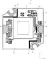
<2.変形例>
次に、本発明の実施形態の変形例について説明する。この変形例は、実施形態と比較して、非形成領域の形状が異なっている。以下の説明では、実施形態との相違点について説明し、実施形態と共通な部分については説明を省略する。<2. Modified example>
Next, a modification of the embodiment of the present invention will be described. This modification differs from the embodiment in the shape of the non-formation area. In the following description, differences from the embodiment will be described, and description of parts common to the embodiment will be omitted.
図4は、本実施形態の変形例の回路基板の平面図である。図4に示されるように、変形例の回路基板1では、基材11は、グランドパターン24上に、略直線状の非形成領域33を含む。本変形例では、非形成領域33は、素子配置領域21から面接触領域22aへ向かう方向と交わる方向に沿って、直線状またはL字状に形成される。詳細には、面接触領域22aのx軸-側では、y軸方向に延びる直線状の非形成領域33が形成される。面接触領域22bの撮像素子43に近い側では、回路基板1のx軸-側の辺の近傍からx軸+側へ延びた後、y軸+側へ延びるL字状の非形成領域33が形成される。面接触領域22cの撮像素子43に近い側では、回路基板1のy軸-側の辺の近傍からy軸+側へ延びた後、x軸+側へ延びるL字状の非形成領域33が形成される。 FIG. 4 is a plan view of a circuit board according to a modification of this embodiment. As shown in FIG. 4, in the modified
上記の変形例の回路基板では、基材11が、略直線状の非形成領域33を含むため、素子配置領域21から面接触領域22へのアンダーフィル接着剤の流れ出しを、連続する非形成領域33によって効果的に抑制することができる。また、非形成領域33を簡易に形成することができる。 In the circuit board of the above modification, since the
<3.補足事項>
以上、本発明の実施形態についての具体的な説明を行った。上記説明では、あくまで一実施形態としての説明であって、本発明の範囲はこの一実施形態に留まらず、当業者が把握可能な範囲にまで広く解釈されるものである。<3. Additional information>
The embodiments of the present invention have been specifically described above. The above description is merely a description of one embodiment, and the scope of the present invention is not limited to this one embodiment, but is to be broadly interpreted to the extent that those skilled in the art can understand.
本実施形態の撮像装置では、回路基板1とレンズ鏡筒42と直接に固定される構成について説明したが、回路基板1とレンズ鏡筒42とが、ねじ、リベット、板ばねもしくはコイルばねなどの付勢部材、またはワッシャなどの他の部材を介して間接に固定される構成であってもよい。 In the imaging device of this embodiment, a configuration in which the
また、本実施形態の回路基板では、非形成領域23にグランドパターン24が形成される構成について説明したが、非形成領域23には、信号線の銅箔12が形成される構成であってもよい。しかしながら、非形成領域23には、電波対策を効果的に行うことが可能なグランドパターン24が形成される構成が好ましい。 Further, in the circuit board of the present embodiment, the configuration in which the
また、本実施形態の回路基板には、固化したアンダーフィル接着剤上には、何も塗布されない構成について説明したが、固化したアンダーフィル接着剤上に、放熱用のグリスが塗布される構成であってもよい。この場合においても、非形成領域23によって、素子配置領域21から面接触領域22への放熱用のグリスの流れ出しを抑制することができる。 Furthermore, in the circuit board of this embodiment, a configuration in which nothing is applied on the solidified underfill adhesive has been described, but a configuration in which heat dissipation grease is applied on the solidified underfill adhesive is also described. There may be. Even in this case, the
また、本実施形態の回路基板において基材上に形成された銅箔12に代えて、銅以外の導電性材料でパターン等が形成されてもよい。 Further, in place of the
本発明は、ケースなどの部材に精度よく固定可能な回路基板として好適に利用される。 INDUSTRIAL APPLICATION This invention is suitably utilized as a circuit board which can be fixed to members, such as a case, with high precision.
1…回路基板
11…基材
12…銅箔
13…レジスト
21…素子配置領域
22…面接触領域
23…非形成領域
24…グランドパターン
33…非形成領域
41…撮像装置
42…レンズ鏡筒
42a…当接面
43…撮像素子
44…レンズ
45…ねじ1...
Claims (5)
Translated fromJapanese回路素子が配置された基材と、
前記基材上に導電体で形成されたパターンと、
前記基材または前記パターン上に形成された絶縁層と、
前記基材、前記パターンまたは前記絶縁層上に形成された、前記回路素子の固定を補強する補強材と、を備え、
前記基材は、平面視において、
前記回路素子が配置される素子配置領域と、
前記他の部材と面接触する面接触領域と、
前記素子配置領域と前記面接触領域との間に位置し、前記絶縁層が形成されない非形成領域と、を含み、
前記非形成領域は、前記基材に、平面視において、前記面接触領域の外周に沿って前記面接触領域を取り囲むように配置された複数の円形状の領域が千鳥状に配置されることで形成される、
回路基板。A circuit board fixed to another member,
a base material on which circuit elements are arranged;
a pattern formed of a conductor on the base material;
an insulating layer formed on the base material or the pattern;
a reinforcing material formed on the base material, the pattern, or the insulating layer to reinforce fixation of the circuit element,
In plan view, the base material has the following features:
an element placement area where the circuit element is placed;
a surface contact area that makes surface contact with the other member;
a non-formation region located between the element arrangement region and the surface contact region,where the insulating layer is not formed;
The non-formation area is formed by arranging a plurality of circular areas in a staggered manner on the base material, which are arranged along the outer periphery of the surface contact area so as to surround the surface contact area in plan view. It is formed,
circuit board.
回路素子が配置された基材と、 a base material on which circuit elements are arranged;
前記基材上に導電体で形成されたパターンと、 a pattern formed of a conductor on the base material;
前記基材または前記パターン上に形成された絶縁層と、 an insulating layer formed on the base material or the pattern;
前記基材、前記パターンまたは前記絶縁層上に形成された、前記回路素子の固定を補強する補強材と、を備え、 a reinforcing material formed on the base material, the pattern, or the insulating layer to reinforce fixation of the circuit element,
前記基材は、平面視において、 In plan view, the base material has the following features:
前記回路素子が配置される素子配置領域と、 an element placement area where the circuit element is placed;
前記他の部材と面接触する面接触領域と、 a surface contact area that makes surface contact with the other member;
前記素子配置領域と前記面接触領域との間に位置し、前記絶縁層が形成されない非形成領域と、を含み、 a non-formation region located between the element arrangement region and the surface contact region, where the insulating layer is not formed;
前記非形成領域は、前記基材に、平面視において、前記面接触領域の外周に沿って前記面接触領域を取り囲むようにL字状に配置されることで形成される、 The non-formation area is formed on the base material by being arranged in an L-shape so as to surround the surface contact area along the outer periphery of the surface contact area in a plan view.
回路基板。 circuit board.
請求項1または請求項2に記載の回路基板。The grounded pattern is formed in the non-formation area,
The circuit board according to claim 1or claim 2 .
請求項1から請求項3のいずれか1項に記載の回路基板。the circuit element is an image sensor;
The circuit board accordingto any one of claims 1 to 3 .
前記ケースに固定される、請求項1から請求項4のいずれか1項に記載の回路基板と、
前記ケースに保持され、前記回路素子と対向するレンズと、を備える、
撮像装置。The other member is a case,
The circuit board according to any one of claims 1 to4 , which is fixed to the case;
a lens held in the case and facing the circuit element;
Imaging device.
Priority Applications (1)
| Application Number | Priority Date | Filing Date | Title |
|---|---|---|---|
| JP2019171032AJP7373336B2 (en) | 2019-09-20 | 2019-09-20 | Circuit board and imaging device |
Applications Claiming Priority (1)
| Application Number | Priority Date | Filing Date | Title |
|---|---|---|---|
| JP2019171032AJP7373336B2 (en) | 2019-09-20 | 2019-09-20 | Circuit board and imaging device |
Publications (2)
| Publication Number | Publication Date |
|---|---|
| JP2021048333A JP2021048333A (en) | 2021-03-25 |
| JP7373336B2true JP7373336B2 (en) | 2023-11-02 |
Family
ID=74876593
Family Applications (1)
| Application Number | Title | Priority Date | Filing Date |
|---|---|---|---|
| JP2019171032AActiveJP7373336B2 (en) | 2019-09-20 | 2019-09-20 | Circuit board and imaging device |
Country Status (1)
| Country | Link |
|---|---|
| JP (1) | JP7373336B2 (en) |
Families Citing this family (1)
| Publication number | Priority date | Publication date | Assignee | Title |
|---|---|---|---|---|
| JP2022147187A (en) | 2021-03-23 | 2022-10-06 | 株式会社山田製作所 | steering device |
Citations (6)
| Publication number | Priority date | Publication date | Assignee | Title |
|---|---|---|---|---|
| JP2007299929A (en) | 2006-04-28 | 2007-11-15 | Matsushita Electric Ind Co Ltd | Optical device apparatus and optical device module using the same |
| JP2009059786A (en) | 2007-08-30 | 2009-03-19 | Kyocera Corp | Portable electronic devices |
| JP2009302312A (en) | 2008-06-13 | 2009-12-24 | Yamaha Corp | Package for semiconductor device, package, semiconductor device, and microphone package |
| JP2013198051A (en) | 2012-03-22 | 2013-09-30 | Sony Corp | Electro-optical device and optical apparatus |
| JP2017011217A (en) | 2015-06-25 | 2017-01-12 | シャープ株式会社 | Solid-state imaging device and camera module |
| JP2020145318A (en) | 2019-03-06 | 2020-09-10 | 三菱電機株式会社 | High-frequency package |
- 2019
- 2019-09-20JPJP2019171032Apatent/JP7373336B2/enactiveActive
Patent Citations (6)
| Publication number | Priority date | Publication date | Assignee | Title |
|---|---|---|---|---|
| JP2007299929A (en) | 2006-04-28 | 2007-11-15 | Matsushita Electric Ind Co Ltd | Optical device apparatus and optical device module using the same |
| JP2009059786A (en) | 2007-08-30 | 2009-03-19 | Kyocera Corp | Portable electronic devices |
| JP2009302312A (en) | 2008-06-13 | 2009-12-24 | Yamaha Corp | Package for semiconductor device, package, semiconductor device, and microphone package |
| JP2013198051A (en) | 2012-03-22 | 2013-09-30 | Sony Corp | Electro-optical device and optical apparatus |
| JP2017011217A (en) | 2015-06-25 | 2017-01-12 | シャープ株式会社 | Solid-state imaging device and camera module |
| JP2020145318A (en) | 2019-03-06 | 2020-09-10 | 三菱電機株式会社 | High-frequency package |
Also Published As
| Publication number | Publication date |
|---|---|
| JP2021048333A (en) | 2021-03-25 |
Similar Documents
| Publication | Publication Date | Title |
|---|---|---|
| JP6969595B2 (en) | Imaging unit and imaging device | |
| JP5885690B2 (en) | Electronic components and equipment | |
| JP6296687B2 (en) | Electronic components, electronic modules, and methods for manufacturing them. | |
| US11317027B2 (en) | Imaging unit and imaging apparatus | |
| JP7547541B2 (en) | Image pickup device module, image pickup system, image pickup device package, and manufacturing method | |
| JP2013243340A (en) | Electronic component, mounting member, electronic apparatus, and manufacturing method of these | |
| US11895793B2 (en) | Image pickup unit and imaging apparatus | |
| KR20040095732A (en) | Solid-state imaging device, camera module, and camera-module manufacturing method | |
| CN104769720A (en) | Imaging device, endoscope, semiconductor device, and manufacturing method of semiconductor device | |
| JP4824461B2 (en) | The camera module | |
| US20160135301A1 (en) | Electronic component, electronic module, manufacturing method therefor, and electronic apparatus | |
| JP2010252164A (en) | Solid-state imaging device | |
| US7612333B2 (en) | Imaging apparatus and photoelectric conversion element package retaining unit | |
| JP7373336B2 (en) | Circuit board and imaging device | |
| US20150116975A1 (en) | Electronic component, electronic device, method of manufacturing mounted member, and method of manufacturing electronic component | |
| JP7406314B2 (en) | electronic modules and equipment | |
| JP6576708B2 (en) | Solid-state imaging device and camera module | |
| JP7657614B2 (en) | Imaging unit and imaging device | |
| US12418975B2 (en) | Electronic module, imaging unit and equipment | |
| JP6443494B2 (en) | Imaging unit and imaging apparatus | |
| US20250212547A1 (en) | Module and electronic equipment | |
| WO2014132642A1 (en) | Imaging element and imaging device | |
| JP7695079B2 (en) | electronic equipment | |
| JP2025102606A (en) | Modules and Electronics | |
| JP6111866B2 (en) | Imaging unit and imaging apparatus |
Legal Events
| Date | Code | Title | Description |
|---|---|---|---|
| A621 | Written request for application examination | Free format text:JAPANESE INTERMEDIATE CODE: A621 Effective date:20220914 | |
| A131 | Notification of reasons for refusal | Free format text:JAPANESE INTERMEDIATE CODE: A131 Effective date:20230627 | |
| A977 | Report on retrieval | Free format text:JAPANESE INTERMEDIATE CODE: A971007 Effective date:20230630 | |
| A521 | Request for written amendment filed | Free format text:JAPANESE INTERMEDIATE CODE: A523 Effective date:20230803 | |
| TRDD | Decision of grant or rejection written | ||
| A01 | Written decision to grant a patent or to grant a registration (utility model) | Free format text:JAPANESE INTERMEDIATE CODE: A01 Effective date:20231017 | |
| A61 | First payment of annual fees (during grant procedure) | Free format text:JAPANESE INTERMEDIATE CODE: A61 Effective date:20231023 | |
| R150 | Certificate of patent or registration of utility model | Ref document number:7373336 Country of ref document:JP Free format text:JAPANESE INTERMEDIATE CODE: R150 |