JP7345497B2 - battery pack - Google Patents
battery packDownload PDFInfo
- Publication number
- JP7345497B2 JP7345497B2JP2020557012AJP2020557012AJP7345497B2JP 7345497 B2JP7345497 B2JP 7345497B2JP 2020557012 AJP2020557012 AJP 2020557012AJP 2020557012 AJP2020557012 AJP 2020557012AJP 7345497 B2JP7345497 B2JP 7345497B2
- Authority
- JP
- Japan
- Prior art keywords
- transistor
- oxide
- insulator
- terminal
- semiconductor device
- Prior art date
- Legal status (The legal status is an assumption and is not a legal conclusion. Google has not performed a legal analysis and makes no representation as to the accuracy of the status listed.)
- Active
Links
Images


Classifications
- H—ELECTRICITY
- H02—GENERATION; CONVERSION OR DISTRIBUTION OF ELECTRIC POWER
- H02J—CIRCUIT ARRANGEMENTS OR SYSTEMS FOR SUPPLYING OR DISTRIBUTING ELECTRIC POWER; SYSTEMS FOR STORING ELECTRIC ENERGY
- H02J7/00—Circuit arrangements for charging or depolarising batteries or for supplying loads from batteries
- H02J7/0068—Battery or charger load switching, e.g. concurrent charging and load supply
- H—ELECTRICITY
- H02—GENERATION; CONVERSION OR DISTRIBUTION OF ELECTRIC POWER
- H02J—CIRCUIT ARRANGEMENTS OR SYSTEMS FOR SUPPLYING OR DISTRIBUTING ELECTRIC POWER; SYSTEMS FOR STORING ELECTRIC ENERGY
- H02J7/00—Circuit arrangements for charging or depolarising batteries or for supplying loads from batteries
- H02J7/0029—Circuit arrangements for charging or depolarising batteries or for supplying loads from batteries with safety or protection devices or circuits
- H02J7/00304—Overcurrent protection
- H—ELECTRICITY
- H01—ELECTRIC ELEMENTS
- H01M—PROCESSES OR MEANS, e.g. BATTERIES, FOR THE DIRECT CONVERSION OF CHEMICAL ENERGY INTO ELECTRICAL ENERGY
- H01M10/00—Secondary cells; Manufacture thereof
- H01M10/42—Methods or arrangements for servicing or maintenance of secondary cells or secondary half-cells
- H01M10/425—Structural combination with electronic components, e.g. electronic circuits integrated to the outside of the casing
- H01M10/4264—Structural combination with electronic components, e.g. electronic circuits integrated to the outside of the casing with capacitors
- H—ELECTRICITY
- H01—ELECTRIC ELEMENTS
- H01M—PROCESSES OR MEANS, e.g. BATTERIES, FOR THE DIRECT CONVERSION OF CHEMICAL ENERGY INTO ELECTRICAL ENERGY
- H01M10/00—Secondary cells; Manufacture thereof
- H01M10/42—Methods or arrangements for servicing or maintenance of secondary cells or secondary half-cells
- H01M10/44—Methods for charging or discharging
- H—ELECTRICITY
- H02—GENERATION; CONVERSION OR DISTRIBUTION OF ELECTRIC POWER
- H02J—CIRCUIT ARRANGEMENTS OR SYSTEMS FOR SUPPLYING OR DISTRIBUTING ELECTRIC POWER; SYSTEMS FOR STORING ELECTRIC ENERGY
- H02J7/00—Circuit arrangements for charging or depolarising batteries or for supplying loads from batteries
- H02J7/0029—Circuit arrangements for charging or depolarising batteries or for supplying loads from batteries with safety or protection devices or circuits
- H02J7/0031—Circuit arrangements for charging or depolarising batteries or for supplying loads from batteries with safety or protection devices or circuits using battery or load disconnect circuits
- H—ELECTRICITY
- H03—ELECTRONIC CIRCUITRY
- H03K—PULSE TECHNIQUE
- H03K17/00—Electronic switching or gating, i.e. not by contact-making and –breaking
- H03K17/08—Modifications for protecting switching circuit against overcurrent or overvoltage
- H03K17/082—Modifications for protecting switching circuit against overcurrent or overvoltage by feedback from the output to the control circuit
- H03K17/0822—Modifications for protecting switching circuit against overcurrent or overvoltage by feedback from the output to the control circuit in field-effect transistor switches
- H—ELECTRICITY
- H10—SEMICONDUCTOR DEVICES; ELECTRIC SOLID-STATE DEVICES NOT OTHERWISE PROVIDED FOR
- H10D—INORGANIC ELECTRIC SEMICONDUCTOR DEVICES
- H10D30/00—Field-effect transistors [FET]
- H10D30/60—Insulated-gate field-effect transistors [IGFET]
- H10D30/67—Thin-film transistors [TFT]
- H—ELECTRICITY
- H10—SEMICONDUCTOR DEVICES; ELECTRIC SOLID-STATE DEVICES NOT OTHERWISE PROVIDED FOR
- H10D—INORGANIC ELECTRIC SEMICONDUCTOR DEVICES
- H10D30/00—Field-effect transistors [FET]
- H10D30/60—Insulated-gate field-effect transistors [IGFET]
- H10D30/67—Thin-film transistors [TFT]
- H10D30/6729—Thin-film transistors [TFT] characterised by the electrodes
- H10D30/673—Thin-film transistors [TFT] characterised by the electrodes characterised by the shapes, relative sizes or dispositions of the gate electrodes
- H10D30/6733—Multi-gate TFTs
- H—ELECTRICITY
- H10—SEMICONDUCTOR DEVICES; ELECTRIC SOLID-STATE DEVICES NOT OTHERWISE PROVIDED FOR
- H10D—INORGANIC ELECTRIC SEMICONDUCTOR DEVICES
- H10D30/00—Field-effect transistors [FET]
- H10D30/60—Insulated-gate field-effect transistors [IGFET]
- H10D30/67—Thin-film transistors [TFT]
- H10D30/674—Thin-film transistors [TFT] characterised by the active materials
- H10D30/6755—Oxide semiconductors, e.g. zinc oxide, copper aluminium oxide or cadmium stannate
- H—ELECTRICITY
- H10—SEMICONDUCTOR DEVICES; ELECTRIC SOLID-STATE DEVICES NOT OTHERWISE PROVIDED FOR
- H10D—INORGANIC ELECTRIC SEMICONDUCTOR DEVICES
- H10D84/00—Integrated devices formed in or on semiconductor substrates that comprise only semiconducting layers, e.g. on Si wafers or on GaAs-on-Si wafers
- H10D84/01—Manufacture or treatment
- H10D84/02—Manufacture or treatment characterised by using material-based technologies
- H10D84/03—Manufacture or treatment characterised by using material-based technologies using Group IV technology, e.g. silicon technology or silicon-carbide [SiC] technology
- H10D84/038—Manufacture or treatment characterised by using material-based technologies using Group IV technology, e.g. silicon technology or silicon-carbide [SiC] technology using silicon technology, e.g. SiGe
- H—ELECTRICITY
- H10—SEMICONDUCTOR DEVICES; ELECTRIC SOLID-STATE DEVICES NOT OTHERWISE PROVIDED FOR
- H10D—INORGANIC ELECTRIC SEMICONDUCTOR DEVICES
- H10D84/00—Integrated devices formed in or on semiconductor substrates that comprise only semiconducting layers, e.g. on Si wafers or on GaAs-on-Si wafers
- H10D84/80—Integrated devices formed in or on semiconductor substrates that comprise only semiconducting layers, e.g. on Si wafers or on GaAs-on-Si wafers characterised by the integration of at least one component covered by groups H10D12/00 or H10D30/00, e.g. integration of IGFETs
- H10D84/82—Integrated devices formed in or on semiconductor substrates that comprise only semiconducting layers, e.g. on Si wafers or on GaAs-on-Si wafers characterised by the integration of at least one component covered by groups H10D12/00 or H10D30/00, e.g. integration of IGFETs of only field-effect components
- H10D84/83—Integrated devices formed in or on semiconductor substrates that comprise only semiconducting layers, e.g. on Si wafers or on GaAs-on-Si wafers characterised by the integration of at least one component covered by groups H10D12/00 or H10D30/00, e.g. integration of IGFETs of only field-effect components of only insulated-gate FETs [IGFET]
- H—ELECTRICITY
- H03—ELECTRONIC CIRCUITRY
- H03K—PULSE TECHNIQUE
- H03K2217/00—Indexing scheme related to electronic switching or gating, i.e. not by contact-making or -breaking covered by H03K17/00
- H03K2217/0027—Measuring means of, e.g. currents through or voltages across the switch
- H—ELECTRICITY
- H03—ELECTRONIC CIRCUITRY
- H03K—PULSE TECHNIQUE
- H03K2217/00—Indexing scheme related to electronic switching or gating, i.e. not by contact-making or -breaking covered by H03K17/00
- H03K2217/0072—Low side switches, i.e. the lower potential [DC] or neutral wire [AC] being directly connected to the switch and not via the load
- H—ELECTRICITY
- H03—ELECTRONIC CIRCUITRY
- H03K—PULSE TECHNIQUE
- H03K3/00—Circuits for generating electric pulses; Monostable, bistable or multistable circuits
- H03K3/02—Generators characterised by the type of circuit or by the means used for producing pulses
- H03K3/023—Generators characterised by the type of circuit or by the means used for producing pulses by the use of differential amplifiers or comparators, with internal or external positive feedback
- H03K3/0231—Astable circuits
- Y—GENERAL TAGGING OF NEW TECHNOLOGICAL DEVELOPMENTS; GENERAL TAGGING OF CROSS-SECTIONAL TECHNOLOGIES SPANNING OVER SEVERAL SECTIONS OF THE IPC; TECHNICAL SUBJECTS COVERED BY FORMER USPC CROSS-REFERENCE ART COLLECTIONS [XRACs] AND DIGESTS
- Y02—TECHNOLOGIES OR APPLICATIONS FOR MITIGATION OR ADAPTATION AGAINST CLIMATE CHANGE
- Y02E—REDUCTION OF GREENHOUSE GAS [GHG] EMISSIONS, RELATED TO ENERGY GENERATION, TRANSMISSION OR DISTRIBUTION
- Y02E60/00—Enabling technologies; Technologies with a potential or indirect contribution to GHG emissions mitigation
- Y02E60/10—Energy storage using batteries
Landscapes
- Engineering & Computer Science (AREA)
- Power Engineering (AREA)
- General Chemical & Material Sciences (AREA)
- Chemical & Material Sciences (AREA)
- Chemical Kinetics & Catalysis (AREA)
- Electrochemistry (AREA)
- Manufacturing & Machinery (AREA)
- Microelectronics & Electronic Packaging (AREA)
- Metal-Oxide And Bipolar Metal-Oxide Semiconductor Integrated Circuits (AREA)
- Thin Film Transistor (AREA)
- Charge And Discharge Circuits For Batteries Or The Like (AREA)
- Secondary Cells (AREA)
- Semiconductor Integrated Circuits (AREA)
- Protection Of Static Devices (AREA)
- Semiconductor Memories (AREA)
Description
Translated fromJapanese本発明の一態様は、半導体装置、および半導体装置の動作方法に関する。また、本発明の一態様は、電池制御回路、電池保護回路、蓄電装置、および電子機器に関する。One embodiment of the present invention relates to a semiconductor device and a method of operating the semiconductor device. Further, one embodiment of the present invention relates to a battery control circuit, a battery protection circuit, a power storage device, and an electronic device.
なお本発明の一態様は、上記の技術分野に限定されない。本明細書等で開示する発明の技術分野は、物、方法、または、製造方法に関するものである。または、本発明の一態様は、プロセス、マシン、マニュファクチャ、または、組成物(コンポジション・オブ・マター)に関するものである。そのため、より具体的に本明細書で開示する本発明の一態様の技術分野としては、表示装置、発光装置、蓄電装置、撮像装置、記憶装置、それらの駆動方法、または、それらの製造方法、を一例として挙げることができる。Note that one embodiment of the present invention is not limited to the above technical field. The technical field of the invention disclosed in this specification and the like relates to products, methods, or manufacturing methods. Alternatively, one aspect of the present invention relates to a process, machine, manufacture, or composition of matter. Therefore, more specifically, the technical field of one embodiment of the present invention disclosed in this specification includes a display device, a light emitting device, a power storage device, an imaging device, a storage device, a driving method thereof, or a manufacturing method thereof; can be cited as an example.
なお、本明細書等において半導体装置とは、半導体特性を利用することで機能しうるもの全般を指す。よって、トランジスタやダイオードなどの半導体素子や半導体回路は半導体装置である。また、表示装置、発光装置、照明装置、電気光学装置、および電子機器などは、半導体素子や半導体回路を含む場合がある。よって、表示装置、発光装置、照明装置、電気光学装置、撮像装置、および電子機器なども、半導体装置と呼ばれる場合がある。Note that in this specification and the like, a semiconductor device refers to any device that can function by utilizing semiconductor characteristics. Therefore, semiconductor elements and semiconductor circuits such as transistors and diodes are semiconductor devices. Furthermore, display devices, light emitting devices, lighting devices, electro-optical devices, electronic devices, and the like may include semiconductor elements and semiconductor circuits. Therefore, display devices, light emitting devices, lighting devices, electro-optical devices, imaging devices, electronic devices, and the like may also be called semiconductor devices.
近年、リチウムイオン二次電池、リチウムイオンキャパシタ、空気電池等、種々の蓄電装置の開発が盛んに行われている。特に高出力、高エネルギー密度であるリチウムイオン二次電池は、携帯電話、スマートフォン、タブレット、もしくはノート型コンピュータ等の携帯情報端末、ゲーム装置、携帯音楽プレーヤ、デジタルカメラ、医療機器、または、ハイブリッド車(HEV)、電気自動車(EV)、もしくはプラグインハイブリッド車(PHEV)等の次世代クリーンエネルギー自動車、電動バイクなど、半導体産業の発展と併せて急速にその需要が拡大し、充電可能なエネルギーの供給源として現代の情報化社会に不可欠なものとなっている。In recent years, various power storage devices, such as lithium ion secondary batteries, lithium ion capacitors, and air batteries, have been actively developed. In particular, lithium ion secondary batteries with high output and high energy density are used in mobile information terminals such as mobile phones, smartphones, tablets, and notebook computers, game devices, portable music players, digital cameras, medical equipment, and hybrid vehicles. Demand for next-generation clean energy vehicles such as (HEV), electric vehicles (EV), or plug-in hybrid vehicles (PHEV), and electric motorcycles is rapidly expanding along with the development of the semiconductor industry, and the demand for rechargeable energy vehicles is rapidly increasing. As a supply source, it has become indispensable in the modern information society.
特許文献1には、過電流を検出して二次電池の充放電を制御する半導体装置が示されている。
特許文献1に示されている構成では、過電流の検出に定電流源を用いるため消費電力が増加しやすい。また、特許文献1に示されている構成では、過電流の検出において、放電用トランジスタおよび充電用トランジスタそれぞれの抵抗値ばらつきの影響を受けるため、検出精度の向上が難しい。In the configuration shown in
本発明の一態様は、消費電力が低減された半導体装置などを提供することを課題の一つとする。または、過電流の検出精度の良好な半導体装置などを提供することを課題の一つとする。または、動作の安定した半導体装置などを提供することを課題の一つとする。または、信頼性の良好な半導体装置などを提供することを課題の一つとする。または、生産性が良好な半導体装置などを提供することを課題の一つとする。または、新規な半導体装置などを提供することを課題の一つとする。An object of one embodiment of the present invention is to provide a semiconductor device or the like with reduced power consumption. Another object of the present invention is to provide a semiconductor device with good overcurrent detection accuracy. Alternatively, one of the challenges is to provide a semiconductor device with stable operation. Alternatively, one of the challenges is to provide a semiconductor device or the like with good reliability. Alternatively, one of the challenges is to provide a semiconductor device or the like with good productivity. Alternatively, one of the challenges is to provide a new semiconductor device or the like.
なお、これらの課題の記載は、他の課題の存在を妨げるものではない。なお、本発明の一態様は、これらの課題の全てを解決する必要はないものとする。なお、これら以外の課題は、明細書、図面、請求項などの記載から、自ずと明らかとなるものであり、明細書、図面、請求項などの記載から、これら以外の課題を抽出することが可能である。Note that the description of these issues does not preclude the existence of other issues. Note that one embodiment of the present invention does not need to solve all of these problems. Note that issues other than these will naturally become clear from the description, drawings, claims, etc., and it is possible to extract issues other than these from the description, drawings, claims, etc. It is.
本発明の一態様は、ノードND1と、ノードND2と、抵抗と、容量と、比較回路と、を有する半導体装置であって、抵抗は、二次電池の正極または負極の一方と、第1端子の間に、直列かつ電気的に接続される。抵抗は、二次電池の正極または負極の一方と第1端子の間に流れる電流を第1電圧に変換する機能を有する。第1電圧は、容量を介してノードND2の電圧に加算される。比較回路は、ノードND1の電圧とノードND2の電圧を比較する機能を有する。比較回路は、ノードND2の電圧がノードND1の電圧よりも大きい場合、過電流を検知したことを知らせる信号を出力する。One embodiment of the present invention is a semiconductor device including a node ND1, a node ND2, a resistor, a capacitor, and a comparison circuit, wherein the resistor is connected to one of a positive electrode or a negative electrode of a secondary battery and a first terminal. are electrically connected in series between them. The resistor has a function of converting the current flowing between the first terminal and one of the positive electrode or the negative electrode of the secondary battery into a first voltage. The first voltage is added to the voltage at node ND2 via the capacitor. The comparison circuit has a function of comparing the voltage of the node ND1 and the voltage of the node ND2. The comparison circuit outputs a signal indicating that an overcurrent has been detected when the voltage at the node ND2 is higher than the voltage at the node ND1.
本発明の別の一態様は、第1乃至第4トランジスタと、コンパレータと、を有し、第1トランジスタのソースまたはドレインの一方は、コンパレータの非反転入力端子と電気的に接続され、第2トランジスタのソースまたはドレインの一方は、コンパレータの反転入力端子と電気的に接続され、第3トランジスタのソースまたはドレインの一方は、第4トランジスタのソースまたはドレインの一方と電気的に接続され、第3トランジスタのソースまたはドレインの他方と、第4トランジスタのソースまたはドレインの他方の間に抵抗を有する半導体装置である。Another embodiment of the present invention includes first to fourth transistors and a comparator, one of the source or drain of the first transistor is electrically connected to the non-inverting input terminal of the comparator, and the second One of the source or drain of the transistor is electrically connected to the inverting input terminal of the comparator, one of the source or drain of the third transistor is electrically connected to one of the source or drain of the fourth transistor, and the third The semiconductor device has a resistance between the other of the source or drain of the transistor and the other of the source or drain of the fourth transistor.
抵抗の抵抗値は、1mΩ以上10Ω以下とすればよい。また、第1トランジスタのソースまたはドレインの一方に第1容量を有してもよい。第1容量の容量値は0.01fF以上100pF以下とすればよい。また、第2トランジスタのソースまたはドレインの一方と第3トランジスタのソースまたはドレインの一方の間に第2容量を有してもよい。第2容量の容量値は0.01fF以上100pF以下とすればよい。The resistance value of the resistor may be 1 mΩ or more and 10Ω or less. Further, the first transistor may have a first capacitor at either the source or the drain. The capacitance value of the first capacitor may be greater than or equal to 0.01 fF and less than or equal to 100 pF. Further, a second capacitor may be provided between one of the source or drain of the second transistor and one of the source or drain of the third transistor. The capacitance value of the second capacitor may be 0.01 fF or more and 100 pF or less.
第1および第2トランジスタは、半導体層に酸化物半導体を含むことが好ましい。第3および第4トランジスタは、半導体層に酸化物半導体を含むことが好ましい。Preferably, the first and second transistors include an oxide semiconductor in their semiconductor layers. Preferably, the third and fourth transistors include an oxide semiconductor in their semiconductor layers.
第1乃至第4トランジスタの少なくとも一つは、マルチゲート型のトランジスタであってもよい。At least one of the first to fourth transistors may be a multi-gate transistor.
第1トランジスタのソースまたはドレインの他方に供給される電位は、第2トランジスタのソースまたはドレインの他方に供給される電位よりも低いことが好ましい。The potential supplied to the other of the source or drain of the first transistor is preferably lower than the potential supplied to the other of the source or drain of the second transistor.
本発明の別の一態様は、第1トランジスタと、第2トランジスタと、コンパレータと、を有し、第1トランジスタのソースまたはドレインの一方は、コンパレータの非反転入力端子と電気的に接続され、第1トランジスタのソースまたはドレインの一方に第1容量を有し、第2トランジスタのソースまたはドレインの一方は、コンパレータの反転入力端子と電気的に接続され、第2トランジスタのソースまたはドレインの一方と抵抗の間に第2容量を備える半導体装置である。Another embodiment of the present invention includes a first transistor, a second transistor, and a comparator, and one of the source or drain of the first transistor is electrically connected to a non-inverting input terminal of the comparator; One of the source or drain of the first transistor has a first capacitor, one of the source or drain of the second transistor is electrically connected to the inverting input terminal of the comparator, and one of the source or drain of the second transistor is electrically connected to the inverting input terminal of the comparator. This is a semiconductor device including a second capacitor between resistors.
また、本発明の別の一態様は、可撓性基板に設けられた半導体装置と、絶縁シートと、二次電池と、を含む電池パックである。Another embodiment of the present invention is a battery pack that includes a semiconductor device provided on a flexible substrate, an insulating sheet, and a secondary battery.
上記電池パックに、第1ダイオードと、第2ダイオードと、第2抵抗と、第3容量と、を設けてもよい。第1ダイオードのカソードは二次電池の正極と電気的に接続し、第1ダイオードのアノードは第2ダイオードのカソードと電気的に接続し、第2ダイオードのアノードは二次電池の負極と電気的に接続する。また、第2抵抗は、第1ダイオードのアノードとコンパレータの出力端子の間に設け、第3容量は、第2ダイオードと並列に接続する。The battery pack may include a first diode, a second diode, a second resistor, and a third capacitor. The cathode of the first diode is electrically connected to the positive electrode of the secondary battery, the anode of the first diode is electrically connected to the cathode of the second diode, and the anode of the second diode is electrically connected to the negative electrode of the secondary battery. Connect to. Further, the second resistor is provided between the anode of the first diode and the output terminal of the comparator, and the third capacitor is connected in parallel with the second diode.
第1ダイオードおよび第2ダイオードの一方または双方を、トランジスタで構成することもできる。One or both of the first diode and the second diode can also be configured with a transistor.
本発明の一態様によれば、消費電力が低減された半導体装置などを提供することができる。または、過電流の検出精度の良好な半導体装置などを提供することができる。または、動作の安定した半導体装置などを提供することができる。または、信頼性の良好な半導体装置などを提供することができる。または、生産性が良好な半導体装置などを提供することができる。または、新規な半導体装置などを提供することができる。According to one aspect of the present invention, a semiconductor device or the like with reduced power consumption can be provided. Alternatively, it is possible to provide a semiconductor device with good overcurrent detection accuracy. Alternatively, it is possible to provide a semiconductor device with stable operation. Alternatively, a highly reliable semiconductor device or the like can be provided. Alternatively, a semiconductor device or the like with good productivity can be provided. Alternatively, a new semiconductor device or the like can be provided.
なお、これらの効果の記載は、他の効果の存在を妨げるものではない。なお、本発明の一態様は、これらの効果の全てを有する必要はない。なお、これら以外の効果は、明細書、図面、請求項などの記載から、自ずと明らかとなるものであり、明細書、図面、請求項などの記載から、これら以外の効果を抽出することが可能である。Note that the description of these effects does not preclude the existence of other effects. Note that one embodiment of the present invention does not need to have all of these effects. Note that effects other than these will become obvious from the description, drawings, claims, etc., and effects other than these can be extracted from the description, drawings, claims, etc. It is.
図1は、半導体装置の構成例を示す図である。
図2Aおよび図2Bは、半導体装置の動作例を示す図である。
図3Aおよび図3Bは、半導体装置の動作例を示す図である。
図4Aおよび図4Bは、半導体装置の構成例を示す図である。
図5A乃至図5Dは、トランジスタの回路記号を示す図である。
図6は、半導体装置の構成例を示す図である。
図7Aおよび図7Bは、半導体装置の動作例を示す図である。
図8Aおよび図8Bは、半導体装置の動作例を示す図である。
図9は、半導体装置の構成例を示す図である。
図10Aおよび図10Bは、半導体装置の動作例を示す図である。
図11Aおよび図11Bは、半導体装置の動作例を示す図である。
図12は、半導体装置の構成例を示す図である。
図13Aおよび図13Bは、半導体装置の動作例を示す図である。
図14Aおよび図14Bは、半導体装置の動作例を示す図である。
図15は、半導体装置の構成例を示す図である。
図16は、半導体装置の構成例を示す図である。
図17は、半導体装置の構成例を示す図である。
図18A乃至図18Dは、保護装置の等価回路を示す図である。
図19Aおよび図19Bは、保護装置の等価回路を示す図である。
図20Aおよび図20Bは、保護装置の等価回路を示す図である。
図21A乃至図21Cは、保護装置の等価回路を示す図である。
図22は、半導体装置の構成例を示す図である。
図23A乃至図23Cは、保護装置の等価回路を示す図である。
図24は、半導体装置の構成例を示す図である。
図25は、保護装置の等価回路を示す図である。
図26は、半導体装置の構成例を示す図である。
図27は、半導体装置の構成例を示す図である。
図28は、保護装置の等価回路を示す図である。
図29は、半導体装置の構成例を示す図である。
図30は、半導体装置の構成例を示す図である。
図31A乃至図31Cは、トランジスタの構造例を示す図である。
図32A乃至図32Cは、トランジスタの構造例を示す図である。
図33A乃至図33Cは、トランジスタの構造例を示す図である。
図34A乃至図34Cは、二次電池の構造例を示す図である。
図35A乃至図35Cは、二次電池の構造例を示す図である。
図36Aおよび図36Bは、捲回体および二次電池の構造例を示す図である。
図37は、電子機器の一例を示す図である。FIG. 1 is a diagram showing an example of the configuration of a semiconductor device.
2A and 2B are diagrams illustrating an example of the operation of a semiconductor device.
3A and 3B are diagrams illustrating an example of the operation of a semiconductor device.
4A and 4B are diagrams illustrating a configuration example of a semiconductor device.
5A to 5D are diagrams showing circuit symbols of transistors.
FIG. 6 is a diagram showing a configuration example of a semiconductor device.
7A and 7B are diagrams illustrating an example of the operation of a semiconductor device.
8A and 8B are diagrams illustrating an example of the operation of a semiconductor device.
FIG. 9 is a diagram showing a configuration example of a semiconductor device.
10A and 10B are diagrams illustrating an example of the operation of a semiconductor device.
FIGS. 11A and 11B are diagrams illustrating an example of the operation of a semiconductor device.
FIG. 12 is a diagram showing a configuration example of a semiconductor device.
13A and 13B are diagrams illustrating an example of the operation of a semiconductor device.
14A and 14B are diagrams illustrating an example of the operation of a semiconductor device.
FIG. 15 is a diagram showing a configuration example of a semiconductor device.
FIG. 16 is a diagram showing a configuration example of a semiconductor device.
FIG. 17 is a diagram showing a configuration example of a semiconductor device.
18A to 18D are diagrams showing equivalent circuits of the protection device.
19A and 19B are diagrams showing equivalent circuits of the protection device.
20A and 20B are diagrams showing equivalent circuits of the protection device.
21A to 21C are diagrams showing equivalent circuits of the protection device.
FIG. 22 is a diagram showing a configuration example of a semiconductor device.
23A to 23C are diagrams showing equivalent circuits of the protection device.
FIG. 24 is a diagram showing a configuration example of a semiconductor device.
FIG. 25 is a diagram showing an equivalent circuit of the protection device.
FIG. 26 is a diagram showing a configuration example of a semiconductor device.
FIG. 27 is a diagram showing a configuration example of a semiconductor device.
FIG. 28 is a diagram showing an equivalent circuit of the protection device.
FIG. 29 is a diagram showing a configuration example of a semiconductor device.
FIG. 30 is a diagram showing a configuration example of a semiconductor device.
31A to 31C are diagrams illustrating structural examples of transistors.
32A to 32C are diagrams illustrating structural examples of transistors.
33A to 33C are diagrams showing structural examples of transistors.
34A to 34C are diagrams showing structural examples of secondary batteries.
35A to 35C are diagrams showing structural examples of secondary batteries.
36A and 36B are diagrams showing structural examples of a wound body and a secondary battery.
FIG. 37 is a diagram illustrating an example of an electronic device.
実施の形態について、図面を用いて詳細に説明する。但し、本発明は以下の説明に限定されず、本発明の趣旨およびその範囲から逸脱することなくその形態および詳細を様々に変更し得ることは当業者であれば容易に理解される。従って、本発明は以下に示す実施の形態の記載内容に限定して解釈されるものではない。なお、以下に説明する発明の構成において、同一部分または同様な機能を有する部分には同一の符号を異なる図面間で共通して用い、その繰り返しの説明は省略する。Embodiments will be described in detail using the drawings. However, those skilled in the art will easily understand that the present invention is not limited to the following description, and that the form and details thereof can be changed in various ways without departing from the spirit and scope of the present invention. Therefore, the present invention should not be interpreted as being limited to the contents described in the embodiments shown below. In the configuration of the invention described below, the same parts or parts having similar functions are designated by the same reference numerals in different drawings, and repeated explanation thereof will be omitted.
また、図面等において示す各構成の、位置、大きさ、範囲などは、発明の理解を容易とするため、実際の位置、大きさ、範囲などを表していない場合がある。このため、開示する発明は、必ずしも、図面等に開示された位置、大きさ、範囲などに限定されない。例えば、実際の製造工程において、エッチングなどの処理によりレジストマスクなどが意図せずに目減りすることがあるが、理解を容易とするために図に反映しないことがある。Further, the position, size, range, etc. of each structure shown in the drawings etc. may not represent the actual position, size, range, etc. in order to facilitate understanding of the invention. Therefore, the disclosed invention is not necessarily limited to the position, size, range, etc. disclosed in the drawings or the like. For example, in an actual manufacturing process, a resist mask or the like may be unintentionally reduced due to a process such as etching, but this may not be reflected in the diagram for ease of understanding.
また、上面図(「平面図」ともいう)や斜視図などにおいて、図面をわかりやすくするために、一部の構成要素の記載を省略する場合がある。In addition, in top views (also referred to as "plan views"), perspective views, and the like, some components may be omitted in order to make the drawings easier to understand.
また、本明細書等において「電極」や「配線」の用語は、これらの構成要素を機能的に限定するものではない。例えば、「電極」は「配線」の一部として用いられることがあり、その逆もまた同様である。さらに、「電極」や「配線」の用語は、複数の「電極」や「配線」が一体となって形成されている場合なども含む。Further, in this specification and the like, the terms "electrode" and "wiring" do not functionally limit these components. For example, an "electrode" may be used as part of a "wiring" and vice versa. Furthermore, the terms "electrode" and "wiring" include cases where a plurality of "electrodes" and "wiring" are formed integrally.
また、本明細書等において、電気回路における「端子」とは、電流の入力または出力、電圧の入力または出力、もしくは、信号の受信または送信が行なわれる部位を言う。よって、配線または電極の一部が端子として機能する場合がある。Furthermore, in this specification and the like, a "terminal" in an electric circuit refers to a site where current is input or output, voltage is input or output, or signal is received or transmitted. Therefore, part of the wiring or electrode may function as a terminal.
なお、本明細書等において「上」や「下」の用語は、構成要素の位置関係が直上または直下で、かつ、直接接していることを限定するものではない。例えば、「絶縁層A上の電極B」の表現であれば、絶縁層Aの上に電極Bが直接接して形成されている必要はなく、絶縁層Aと電極Bとの間に他の構成要素を含むものを除外しない。Note that in this specification and the like, the terms "above" and "below" do not limit the positional relationship of components to be directly above or below, and in direct contact with each other. For example, if the expression is "electrode B on insulating layer A," electrode B does not need to be formed directly on insulating layer A, and there is no need to form another structure between insulating layer A and electrode B. Don't exclude things that contain elements.
また、ソースおよびドレインの機能は、異なる極性のトランジスタを採用する場合や、回路動作において電流の方向が変化する場合など、動作条件などによって互いに入れ替わるため、いずれがソースまたはドレインであるかを限定することが困難である。このため、本明細書においては、ソースおよびドレインの用語は、入れ替えて用いることができるものとする。In addition, the functions of the source and drain may be interchanged depending on operating conditions, such as when transistors with different polarities are used or when the direction of current changes during circuit operation, so it is difficult to determine which is the source or drain. It is difficult to do so. Therefore, in this specification, the terms source and drain can be used interchangeably.
また、本明細書等において、「電気的に接続」には、直接接続している場合と、「何らかの電気的作用を有するもの」を介して接続されている場合が含まれる。ここで、「何らかの電気的作用を有するもの」は、接続対象間での電気信号の授受を可能とするものであれば、特に制限を受けない。よって、「電気的に接続する」と表現される場合であっても、現実の回路においては、物理的な接続部分がなく、配線が延在しているだけの場合もある。Furthermore, in this specification and the like, "electrically connected" includes a case of direct connection and a case of connection via "something that has some kind of electrical effect." Here, "something that has some kind of electrical effect" is not particularly limited as long as it enables transmission and reception of electrical signals between connected objects. Therefore, even if it is expressed as "electrically connected," in an actual circuit, there may be no physical connection part, and there may be only extended wiring.
また、本明細書等において、「平行」とは、例えば、二つの直線が-10°以上10°以下の角度で配置されている状態をいう。従って、-5°以上5°以下の場合も含まれる。また、「垂直」および「直交」とは、例えば、二つの直線が80°以上100°以下の角度で配置されている状態をいう。従って、85°以上95°以下の場合も含まれる。Furthermore, in this specification and the like, "parallel" refers to, for example, a state in which two straight lines are arranged at an angle of -10° or more and 10° or less. Therefore, cases where the angle is greater than or equal to -5° and less than or equal to 5° are also included. Moreover, "perpendicular" and "orthogonal" refer to, for example, a state in which two straight lines are arranged at an angle of 80° or more and 100° or less. Therefore, cases where the angle is greater than or equal to 85° and less than or equal to 95° are also included.
なお、本明細書等において、計数値および計量値に関して「同一」、「同じ」、「等しい」または「均一」などと言う場合は、明示されている場合を除き、プラスマイナス20%の誤差を含むものとする。In addition, in this specification etc., when referring to count values and measurement values as "same", "same", "equal", "uniform", etc., unless clearly specified, an error of plus or minus 20% is assumed. shall be included.
また、本明細書において、レジストマスクを形成した後にエッチング処理を行う場合は、特段の説明がない限り、レジストマスクは、エッチング処理終了後に除去するものとする。Further, in this specification, when etching is performed after forming a resist mask, unless otherwise specified, the resist mask is removed after the etching is completed.
また、電圧は、ある電位と、基準の電位(例えば接地電位またはソース電位)との電位差のことを示す場合が多い。よって、電圧と電位は互いに言い換えることが可能な場合が多い。本明細書等では、特段の明示が無いかぎり、電圧と電位を言い換えることができるものとする。Further, voltage often refers to a potential difference between a certain potential and a reference potential (eg, ground potential or source potential). Therefore, voltage and potential can often be interchanged. In this specification and the like, unless otherwise specified, voltage and potential can be interchanged.
なお、「半導体」と表記した場合でも、例えば、導電性が十分低い場合は「絶縁体」としての特性を有する。よって、「半導体」を「絶縁体」に置き換えて用いることも可能である。この場合、「半導体」と「絶縁体」の境界は曖昧であり、両者の厳密な区別は難しい。したがって、本明細書に記載の「半導体」と「絶縁体」は、互いに読み換えることができる場合がある。Note that even when a material is described as a "semiconductor," it has characteristics as an "insulator" if its conductivity is sufficiently low, for example. Therefore, it is also possible to replace "semiconductor" with "insulator". In this case, the boundary between "semiconductor" and "insulator" is ambiguous, and it is difficult to strictly distinguish between the two. Therefore, "semiconductor" and "insulator" described in this specification may be interchangeable.
また、「半導体」と表記した場合でも、例えば、導電性が十分高い場合は「導電体」としての特性を有する。よって、「半導体」を「導電体」に置き換えて用いることも可能である。この場合、「半導体」と「導電体」の境界は曖昧であり、両者の厳密な区別は難しい。したがって、本明細書に記載の「半導体」と「導電体」は、互いに読み換えることができる場合がある。Furthermore, even when a material is described as a "semiconductor", it has characteristics as a "conductor" if its conductivity is sufficiently high, for example. Therefore, "semiconductor" can also be replaced with "conductor". In this case, the boundary between "semiconductor" and "conductor" is ambiguous, and it is difficult to strictly distinguish between the two. Therefore, the terms "semiconductor" and "conductor" described in this specification may be interchangeable.
なお、本明細書等における「第1」、「第2」等の序数詞は、構成要素の混同を避けるために付すものであり、工程順または積層順など、なんらかの順番や順位を示すものではない。また、本明細書等において序数詞が付されていない用語であっても、構成要素の混同を避けるため、特許請求の範囲において序数詞が付される場合がある。また、本明細書等において序数詞が付されている用語であっても、特許請求の範囲において異なる序数詞が付される場合がある。また、本明細書等において序数詞が付されている用語であっても、特許請求の範囲などにおいて序数詞を省略する場合がある。In addition, ordinal numbers such as "first" and "second" in this specification etc. are added to avoid confusion of constituent elements, and do not indicate any order or ranking such as process order or lamination order. . Further, even if a term is not attached with an ordinal number in this specification, etc., an ordinal number may be attached in the claims to avoid confusion of constituent elements. Further, even if a term is given an ordinal number in this specification, a different ordinal number may be used in the claims. Further, even if a term is attached with an ordinal number in this specification or the like, the ordinal number may be omitted in the claims or the like.
なお、本明細書等において、トランジスタの「オン状態」とは、トランジスタのソースとドレインが電気的に短絡しているとみなせる状態(「導通状態」ともいう。)をいう。また、トランジスタの「オフ状態」とは、トランジスタのソースとドレインが電気的に遮断しているとみなせる状態(「非導通状態」ともいう。)をいう。Note that in this specification and the like, the "on state" of a transistor refers to a state in which the source and drain of the transistor can be considered to be electrically shorted (also referred to as a "conductive state"). Further, the "off state" of a transistor refers to a state in which the source and drain of the transistor can be considered to be electrically disconnected (also referred to as a "non-conducting state").
また、本明細書等において、「オン電流」とは、トランジスタがオン状態の時にソースとドレイン間に流れる電流をいう場合がある。また、「オフ電流」とは、トランジスタがオフ状態である時にソースとドレイン間に流れる電流をいう場合がある。Further, in this specification and the like, "on current" may refer to a current flowing between a source and a drain when a transistor is in an on state. Further, "off current" may refer to a current flowing between a source and a drain when a transistor is in an off state.
また、本明細書等において、高電源電位VDD(以下、単に「VDD」または「H電位」ともいう)とは、低電源電位VSSよりも高い電位の電源電位を示す。また、低電源電位VSS(以下、単に「VSS」または「L電位」ともいう)とは、高電源電位VDDよりも低い電位の電源電位を示す。また、接地電位をVDDまたはVSSとして用いることもできる。例えばVDDが接地電位の場合には、VSSは接地電位より低い電位であり、VSSが接地電位の場合には、VDDは接地電位より高い電位である。Furthermore, in this specification and the like, a high power supply potential VDD (hereinafter also simply referred to as "VDD" or "H potential") indicates a power supply potential higher than the low power supply potential VSS. Further, the low power supply potential VSS (hereinafter also simply referred to as "VSS" or "L potential") indicates a power supply potential lower than the high power supply potential VDD. Further, the ground potential can also be used as VDD or VSS. For example, when VDD is a ground potential, VSS is a potential lower than the ground potential, and when VSS is a ground potential, VDD is a potential higher than the ground potential.
また、本明細書等において、ゲートとは、ゲート電極およびゲート配線の一部または全部のことをいう。ゲート配線とは、少なくとも一つのトランジスタのゲート電極と、別の電極や別の配線とを電気的に接続させるための配線のことをいう。Furthermore, in this specification and the like, a gate refers to a part or all of a gate electrode and a gate wiring. A gate wiring refers to a wiring for electrically connecting the gate electrode of at least one transistor to another electrode or another wiring.
また、本明細書等において、ソースとは、ソース領域、ソース電極、およびソース配線の一部または全部のことをいう。ソース領域とは、半導体層のうち、抵抗率が一定値以下の領域のことをいう。ソース電極とは、ソース領域に接続される部分の導電層のことをいう。ソース配線とは、少なくとも一つのトランジスタのソース電極と、別の電極や別の配線とを電気的に接続させるための配線のことをいう。Further, in this specification and the like, a source refers to part or all of a source region, a source electrode, and a source wiring. The source region refers to a region of the semiconductor layer where the resistivity is below a certain value. The source electrode refers to a portion of the conductive layer connected to the source region. The source wiring refers to a wiring for electrically connecting the source electrode of at least one transistor to another electrode or another wiring.
また、本明細書等において、ドレインとは、ドレイン領域、ドレイン電極、及びドレイン配線の一部または全部のことをいう。ドレイン領域とは、半導体層のうち、抵抗率が一定値以下の領域のことをいう。ドレイン電極とは、ドレイン領域に接続される部分の導電層のことをいう。ドレイン配線とは、少なくとも一つのトランジスタのドレイン電極と、別の電極や別の配線とを電気的に接続させるための配線のことをいう。Furthermore, in this specification and the like, the term "drain" refers to part or all of a drain region, a drain electrode, and a drain wiring. The drain region refers to a region of the semiconductor layer where the resistivity is below a certain value. The drain electrode refers to a portion of the conductive layer connected to the drain region. The drain wiring refers to a wiring for electrically connecting the drain electrode of at least one transistor to another electrode or another wiring.
(実施の形態1)
本発明の一態様の半導体装置について、図面を用いて説明する。(Embodiment 1)
A semiconductor device according to one embodiment of the present invention will be described with reference to the drawings.
<半導体装置200Aの構成例>
図1に半導体装置200Aの構成例を示す。半導体装置200Aは、端子201乃至端子204、半導体装置100C、制御回路210、電位生成回路220、抵抗211、容量212、トランジスタ213、トランジスタ214、ダイオード215、およびダイオード216を有する。<Example of configuration of
FIG. 1 shows a configuration example of a
半導体装置100Cは、端子R、端子RFN、端子SH、端子SHB、および端子OUTを有する。また、半導体装置100Cは、コンパレータ101、トランジスタ111乃至トランジスタ114、容量102、容量103、および抵抗121を有する。The
制御回路210は、端子221乃至端子225を有する。抵抗211の一方の端子は端子201および端子203と電気的に接続され、他方の端子は端子221と電気的に接続される。容量212の一方の端子は端子221と電気的に接続され、他方の端子は端子222および端子204と電気的に接続される。
トランジスタ213のソースまたはドレインの一方は端子222および端子204と電気的に接続され、ゲートは端子223と電気的に接続される。ダイオード215のアノードはトランジスタ213のソースまたはドレインの一方と電気的に接続される。ダイオード215のカソードはトランジスタ213のソースまたはドレインの他方と電気的に接続される。One of the source and drain of the
トランジスタ214のソースまたはドレインの一方は、トランジスタ213のソースまたはドレインの他方と電気的に接続され、トランジスタ214のソースまたはドレインの他方は、抵抗121の一方の端子と電気的に接続される。トランジスタ214のゲートは端子224と電気的に接続される。ダイオード216のカソードはトランジスタ214のソースまたはドレインの一方と電気的に接続される。ダイオード216のアノードはトランジスタ214のソースまたはドレインの他方と電気的に接続される。抵抗121の他方の端子は端子202と電気的に接続される。One of the source and the drain of the
電位生成回路220は、端子Rに電位VRを供給する機能と、端子RFNに電位VRFNを供給する機能と、を有する。制御回路210は、電位生成回路220の動作を制御する機能を有する。The
コンパレータ101は、非反転入力端子、反転入力端子、および出力端子を有する。コンパレータ101は、非反転入力端子の電位が反転入力端子の電位よりも高い場合、出力端子に電位VOUTとしてH電位を出力する機能を有する。また、コンパレータ101は、非反転入力端子の電位が反転入力端子の電位よりも低い場合、出力端子に電位VOUTとしてL電位を出力する機能を有する。コンパレータ101は、比較回路として機能する。コンパレータ101の出力端子は、端子OUTと電気的に接続される。また、端子OUTは、配線122を介して制御回路210の端子225と電気的に接続される。
トランジスタ111のソースまたはドレインの一方は、端子Rと電気的に接続され、トランジスタ111のソースまたはドレインの他方は、コンパレータ101の非反転入力端子と電気的に接続される。トランジスタ111のゲートは端子SHと電気的に接続される。One of the source and drain of the
容量102の一方の電極は、コンパレータ101の非反転入力端子と電気的に接続される。容量102の他方の電極は、基準電位または固定電位が供給される。One electrode of the
トランジスタ111のソースまたはドレインの他方、コンパレータ101の非反転入力端子、および容量102の一方の電極が電気的に接続する節点をノードND1という。A node to which the other of the source or drain of the
トランジスタ112のソースまたはドレインの一方は、端子RFNと電気的に接続され、トランジスタ112のソースまたはドレインの他方は、コンパレータ101の反転入力端子と電気的に接続される。トランジスタ112のゲートは端子SHと電気的に接続される。One of the source and drain of the
容量103の一方の電極は、コンパレータ101の反転入力端子と電気的に接続される。One electrode of the
トランジスタ112のソースまたはドレインの他方、コンパレータ101の反転入力端子、および容量103の一方の電極が電気的に接続する節点をノードND2という。A node to which the other of the source or drain of the
トランジスタ113のソースまたはドレインの一方は、抵抗121の一方の端子と電気的に接続され、トランジスタ113のソースまたはドレインの他方は、容量103の他方の電極と電気的に接続される。トランジスタ113のゲートは端子SHと電気的に接続される。One of the source and drain of the
トランジスタ114のソースまたはドレインの一方は、抵抗121の他方の端子と電気的に接続され、トランジスタ114のソースまたはドレインの他方は、容量103の他方の電極と電気的に接続される。トランジスタ114のゲートは端子SHBと電気的に接続される。One of the source and the drain of the
なお、端子SHBには端子SHの反転電位が供給される。例えば、端子SHにH電位が供給される時、端子SHBにL電位が供給される。同様に、端子SHにL電位が供給される時、端子SHBにH電位が供給される。ただし、回路動作上ある特定の期間において、端子SHBおよび端子SHの電位が同電位になる場合もありうる。Note that the inverted potential of the terminal SH is supplied to the terminal SHB. For example, when an H potential is supplied to the terminal SH, an L potential is supplied to the terminal SHB. Similarly, when the L potential is supplied to the terminal SH, the H potential is supplied to the terminal SHB. However, during a certain period of circuit operation, the potentials of the terminal SHB and the terminal SH may become the same potential.
トランジスタ113のソースまたはドレインの他方、トランジスタ114のソースまたはドレインの他方、および容量103の他方の電極が電気的に接続する節点をノードND3という。A node to which the other of the source or drain of the
トランジスタ214のソースまたはドレインの他方、トランジスタ113のソースまたはドレインの一方、および抵抗121の一方の端子が電気的に接続する節点をノードNDAという。トランジスタ114のソースまたはドレインの一方、抵抗121の他方の端子、および端子202が電気的に接続する節点をノードNDBという。A node to which the other of the source or drain of the
また、二次電池300の正極は端子203と電気的に接続され、負極は端子204と電気的に接続される。Further, the positive electrode of the
トランジスタ111乃至トランジスタ114は、チャネルが形成される半導体層に金属酸化物の一種である酸化物半導体を用いたトランジスタ(「OSトランジスタ」ともいう。)を用いることが好ましい。特に、トランジスタ111およびトランジスタ112にOSトランジスタを用いることが好ましい。The
OSトランジスタはオフ電流を極めて少なくすることができる。具体的には、チャネル幅1μm当たりのオフ電流を室温下において1×10-20A未満、好ましくは1×10-22A未満、さらに好ましくは1×10-24A未満とすることができる。OS transistors can have extremely low off-state current. Specifically, the off-state current per 1 μm of channel width can be set to less than 1×10⁻²⁰ A, preferably less than 1×10⁻²² A, and more preferably less than 1×10⁻²⁴ A at room temperature.
また、OSトランジスタは高温環境下でもオフ電流がほとんど増加しない。具体的には室温以上200℃以下の環境温度下でもオフ電流がほとんど増加しない。半導体装置を構成するトランジスタにOSトランジスタを用いることで、高温環境下においても動作が安定し、信頼性の良好な半導体装置を実現できる。Further, the off-state current of the OS transistor hardly increases even in a high temperature environment. Specifically, the off-state current hardly increases even under an environmental temperature of room temperature or higher and 200° C. or lower. By using an OS transistor as a transistor constituting a semiconductor device, it is possible to realize a semiconductor device that operates stably even in a high-temperature environment and has good reliability.
トランジスタ111にOSトランジスタを用いることによって、容量102を小さくすることができる。または、容量102を設けずに、トランジスタなどの寄生容量を容量102に代えて用いることができる。その結果、半導体装置100Cの占有面積を小さくすることができる。よって、半導体装置200Aの占有面積を小さくすることができる。By using an OS transistor as the
一般に、容量は二つの電極が誘電体を介して向かい合う構成を有する。容量値は、向かい合う電極の重畳面積と誘電体の比誘電率に比例し、二つの電極間の距離に反比例する。容量102を設ける場合、容量値が大きすぎると半導体装置200Aの占有面積が大きくなりやすく好ましくない。また、容量102の容量値が大きいと、容量102の充電および放電による消費電力の増加が生じる。Generally, a capacitor has two electrodes facing each other with a dielectric interposed therebetween. The capacitance value is proportional to the overlapping area of the opposing electrodes and the dielectric constant of the dielectric, and is inversely proportional to the distance between the two electrodes. When providing the
容量102を設ける場合、容量102の容量値は、好ましくは0.01fF以上100pF以下、より好ましくは0.05fF以上10pF以下、さらに好ましくは0.1fF以上1pF以下、にすればよい。When the
同様に、トランジスタ112にOSトランジスタを用いることによって、容量103を小さくすることができる。または、容量103を設けずに、トランジスタなどの寄生容量を容量103に代えて用いることができる。Similarly, by using an OS transistor as the
容量103を設ける場合、容量値が大きすぎると半導体装置200Aの占有面積が大きくなりやすく好ましくない。また、容量103の容量値が大きいと、容量103の充電および放電による消費電力の増加が生じる。When providing the
容量103を設ける場合、容量103の容量値は、好ましくは0.01fF以上100pF以下、より好ましくは0.05fF以上10pF以下、さらに好ましくは0.1fF以上1pF以下、にすればよい。When the
また、OSトランジスタは、高温環境下(例えば、50℃以上150℃以下の環境下。)においても、オフ電流が増加しにくい。よって、高温環境下においても、ノードND1およびノードND2に供給された電位(電荷)を長期間保持することができる。Further, the off-state current of the OS transistor is difficult to increase even in a high temperature environment (for example, in an environment of 50° C. or more and 150° C. or less). Therefore, even in a high temperature environment, the potential (charge) supplied to node ND1 and node ND2 can be maintained for a long period of time.
このように、トランジスタ111と容量102によって、記憶素子151が構成される。また、トランジスタ112と容量103によって、記憶素子152が構成される。記憶素子を構成するトランジスタにOSトランジスタを用いた記憶素子を「OSメモリ」と呼ぶ場合がある。In this way, the
また、OSトランジスタは、ソースとドレイン間の絶縁耐圧が高い。よって、トランジスタ213およびトランジスタ214にOSトランジスタを用いることもできる。OSトランジスタを用いることによって、信頼性の良好な半導体装置などを提供できる。Further, the OS transistor has a high dielectric strength voltage between the source and the drain. Therefore, OS transistors can also be used as the
なお、OSトランジスタを用いた充電制御回路、放電制御回路、過電流検知回路、異常検知回路、または二次電池制御システムなどを、BTOS(Battery operating system、またはBattery oxide semiconductor)と呼称する場合がある。Note that a charging control circuit, discharging control circuit, overcurrent detection circuit, abnormality detection circuit, or secondary battery control system using OS transistors is sometimes referred to as BTOS (Battery operating system, or battery oxide semiconductor). .
<半導体装置200Aの動作例>
制御回路210はトランジスタ213のオン状態とオフ状態を選択する機能を有する。また、制御回路210はトランジスタ214のオン状態とオフ状態を選択する機能を有する。<Example of operation of
The
二次電池300の充電は、充電用の外部電源の正極を端子201に接続し、同電源の負極を端子202に接続して行なわれる。また、充電動作は、トランジスタ214をオン状態にして行なわれる。外部電源から供給される電流を、端子203および端子204を経由して、端子201から端子202に流すことで、二次電池300の充電を行なうことができる。The
二次電池300の放電は、端子201および端子202間に負荷を接続して行なわれる。放電動作は、トランジスタ213をオン状態にして行なわれる。放電動作時は、端子204および端子203を経由して、端子202から端子201に電流が流れる。充電動作と放電動作では、抵抗121に流れる電流の向きが逆になる。Discharging of the
また、制御回路210は、二次電池300の充電電圧、温度、などの、二次電池300の状態を検知する機能を有する。また、制御回路210は、二次電池300の状態を検知して、充電動作および放電動作の実行または停止を制御する機能を有する。Further, the
具体的には、制御回路210はトランジスタ213をオフ状態にすることで、二次電池300の放電動作を停止することができる。また、制御回路210はトランジスタ214をオフ状態にすることで、二次電池300の充電動作を停止することができる。トランジスタ213およびトランジスタ214のどちらか一方をオフ状態とすることで、二次電池300の充電動作および放電動作のどちらか一方を停止することができる。Specifically, the
半導体装置100Cは、充電動作中に抵抗121に規定以上の電流(「過電流」ともいう。)が流れた場合、それを検知する機能を有する。具体的には、半導体装置100Cは、充電動作中に過電流を検知するとH電位を出力する。半導体装置100Cの出力(電位VOUT)は、配線122を介して制御回路210の端子225に供給される。半導体装置100Cは、充電動作中の過電流検知回路として機能する。The
半導体装置200Aの制御回路210は、端子225にH電位が供給されると、トランジスタ214をオフ状態にし、充電動作を停止する。過電流による充電を行なわないことで、二次電池300の急激な特性劣化を防ぐことができる。よって、二次電池300の電池寿命を延ばすことができる。また、二次電池300の信頼性を向上することができる。また、二次電池300の安全性を向上することができる。When the H potential is supplied to the terminal 225, the
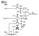
〔半導体装置100Cの動作例〕
半導体装置100Cは、過電流検知回路として機能する。図2および図3を用いて、半導体装置100Cの動作例について説明する。図2および図3は、半導体装置100Cの動作状態を示す図である。[Example of operation of
The
また、図面などにおいて、配線および電極の電位をわかりやすくするため、配線および電極に隣接してH電位を示す“H”、またはL電位を示す“L”を付記する場合がある。また、電位変化が生じた配線および電極には、“H”または“L”を囲み文字で付記する場合がある。また、トランジスタがオフ状態である場合、当該トランジスタに重ねて“×”記号を付記する場合がある。In addition, in drawings and the like, in order to make it easier to understand the potentials of wirings and electrodes, "H" indicating H potential or "L" indicating L potential may be added adjacent to the wirings and electrodes. In addition, "H" or "L" may be added in enclosed letters to wiring and electrodes in which a potential change has occurred. Furthermore, when a transistor is in an off state, an "x" symbol may be added over the transistor.
前述した通り、端子Rには電位VRが供給され、端子RFNには電位VRFNが供給される。本実施の形態では、電位VRを1.1Vとし、電位VRFNを1.25Vとする。As described above, the potential VR is supplied to the terminal R, and the potential VRFN is supplied to the terminal RFN. In this embodiment, the potential VR is set to 1.1V, and the potential VRFN is set to 1.25V.
まず、充電開始前に、端子SHにH電位を供給し、端子SHBにL電位を供給する(図2A参照)。すると、トランジスタ111がオン状態になり、ノードND1の電位が1.1Vになる。また、トランジスタ112がオン状態になり、ノードND2の電位が1.25Vになる。よって、コンパレータ101から出力される電位VOUTがL電位になる。First, before starting charging, an H potential is supplied to the terminal SH, and an L potential is supplied to the terminal SHB (see FIG. 2A). Then, the
また、この時点では、抵抗121に電流が流れていないため、ノードNDAおよびノードNDBの電位は0V(基準電位)である。端子SHにH電位が供給されると、トランジスタ113がオン状態になり、ノードND3の電位は0Vになる。Further, at this point, since no current is flowing through the
次に、端子SHにL電位を供給し、端子SHBにH電位を供給する(図2B参照)。すると、トランジスタ111がオフ状態になり、ノードND1の電位が保持される。同様に、トランジスタ112がオフ状態になり、ノードND2の電位が保持される。また、トランジスタ113もオフ状態になる。Next, the L potential is supplied to the terminal SH, and the H potential is supplied to the terminal SHB (see FIG. 2B). Then, the
次に、充電動作を開始する。充電が始まると、抵抗121に電流ICが流れる(図3A参照)。電流ICはノードNDAからノードNDBに向かって流れるため、充電が始まるとノードNDBの電位は0Vよりも低くなる。よって、ノードND3の電位も0Vより低くなる。Next, a charging operation is started. When charging begins, a current IC flows through the resistor 121 (see FIG. 3A). Since the current IC flows from the node NDA toward the node NDB, the potential of the node NDB becomes lower than 0V when charging starts. Therefore, the potential of node ND3 also becomes lower than 0V.
抵抗121の抵抗値は、好ましくは1mΩ以上10Ω以下、より好ましくは5mΩ以上5Ω以下、さらに好ましくは10mΩ以上1Ω以下、とすればよい。抵抗121の抵抗値を変えることで、半導体装置100Cで検知する過電流の値を変えることができる。また、配線の一部を抵抗121として機能させてもよい。言い換えると、配線抵抗を抵抗121として用いてもよい。The resistance value of the
電流値Ith(A)以上を過電流として検出するための抵抗121の抵抗値RD(Ω)は、数式1で求めることが出来る。The resistance value RD (Ω) of the

例えば、電流Ithの値を1mAに設定する場合、電位VRFNが1.25V、電位VRが1.1Vであるため、数式1より抵抗値RDを150Ωにすればよいことがわかる。For example, when the value of the current Ith is set to 1 mA, the potential VRFN is 1.25 V and the potential VR is 1.1 V, so it can be seen from
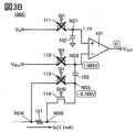
図3Aは、抵抗121の抵抗値RDが150Ωの時に、電流ICとして0.8mAが流れている状態を示している。この場合、ノードNDBの電位は-0.12Vになる。よって、ノードND3の電位も-0.12Vになる。また、ノードND3とノードND2は容量103を介して容量結合している。よって、ノードND2の電位は1.13Vになる。ノードND2の電位はノードND1の電位よりも大きいままである。よって、電位VOUTはL電位のままである。FIG. 3A shows a state in which 0.8 mA is flowing as the current IC when the resistance value RD of the
図3Bは、抵抗121の抵抗値RDが150Ωの時に、電流ICとして1.1mAが流れた時の状態を示している。この場合、ノードNDBの電位は-0.165Vになる。よって、ノードND3の電位も-0.165Vになる。上記と同様の理由により、ノードND2の電位が1.085Vになる。すると、ノードND2の電位がノードND1の電位よりも小さくなり、電位VOUTがH電位になる。FIG. 3B shows a state in which 1.1 mA flows as the current IC when the resistance value RD of the
このようにして、充電動作時の過電流を検知することができる。本発明の一態様の半導体装置100Cは、端子202、トランジスタ213、およびトランジスタ214と直列に接続された抵抗121で過電流の検知を行なう構成である。よって、トランジスタ213およびトランジスタ214の抵抗値ばらつきの影響を受けることなく、精度よく過電流を検知することができる。In this way, overcurrent during charging operation can be detected. A
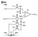
なお、抵抗121は固定抵抗に限らない。図4Aに示すように、抵抗121を可変抵抗にしてもよい。抵抗121を可変抵抗にすることで、電流値Ithの値を任意に変化させることができる。例えば、二次電池300の表面温度に応じて電流値Ithを最適な値に変化させることができる。Note that the
また、トランジスタ111乃至トランジスタ114、トランジスタ213、およびトランジスタ214はスイッチとして機能する。スイッチは、端子間を導通状態(ON)と非導通状態(OFF)に切り替える機能を有しており、電流を流すか流さないかを制御する機能を有する素子である。トランジスタのソースがスイッチの一端に相当し、トランジスタのドレインがスイッチの他端に相当する。よって、例えば、図4Bに示すように、半導体装置100Cに含まれるトランジスタ111乃至トランジスタ114を、スイッチ111s乃至スイッチ114sに置き換えて示すことができる。Further, the
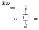
また、トランジスタ111乃至トランジスタ114、トランジスタ213、およびトランジスタ214のそれぞれは、ダブルゲート型のトランジスタであってもよい。図5Aに、ダブルゲート型のトランジスタ150Aの回路記号例を示す。Further, each of the
トランジスタ150Aは、トランジスタTr1とトランジスタTr2を直列に接続した構成を有する。図5Aでは、トランジスタTr1のソースまたはドレインの一方が端子Sと電気的に接続され、トランジスタTr1のソースまたはドレインの他方がトランジスタTr2のソースまたはドレインの一方と電気的に接続され、トランジスタTr2のソースまたはドレインの他方が端子Dと電気的に接続されている状態を示している。また、図5Aでは、トランジスタTr1とトランジスタTr2のゲートが電気的に接続され、かつ、端子Gと電気的に接続されている状態を示している。The
図5Aに示すトランジスタ150Aは、端子Gの電位を変化させることで端子Sと端子D間を導通状態または非導通状態に切り替える機能を有する。よって、ダブルゲート型のトランジスタであるトランジスタ150Aは、トランジスタTr1とトランジスタTr2を内在するもの、1つのトランジスタとして機能する。すなわち、図5Aにおいて、トランジスタ150Aのソースまたはドレインの一方は端子Sと電気的に接続され、ソースまたはドレインの他方は端子Dと電気的に接続され、ゲートは端子Gと電気的に接続されていると言える。The
また、トランジスタ111乃至トランジスタ114、トランジスタ213、およびトランジスタ214のそれぞれは、トリプルゲート型のトランジスタであってもよい。図5Bに、トリプルゲート型のトランジスタ150Bの回路記号例を示す。Further, each of the
トランジスタ150Bは、トランジスタTr1、トランジスタTr2、およびトランジスタTr3を直列に接続した構成を有する。図5Bでは、トランジスタTr1のソースまたはドレインの一方が端子Sと電気的に接続され、トランジスタTr1のソースまたはドレインの他方がトランジスタTr2のソースまたはドレインの一方と電気的に接続され、トランジスタTr2のソースまたはドレインの他方がトランジスタTr3のソースまたはドレインの一方と電気的に接続され、トランジスタTr3のソースまたはドレインの他方が端子Dと電気的に接続されている状態を示している。また、図5Bでは、トランジスタTr1、トランジスタTr2、およびトランジスタTr3のゲートが電気的に接続され、かつ、端子Gと電気的に接続されている状態を示している。The
図5Bに示すトランジスタ150Bは、端子Gの電位を変化させることで端子Sと端子D間を導通状態または非導通状態に切り替える機能を有する。よって、トリプルゲート型のトランジスタであるトランジスタ150Bは、トランジスタTr1、トランジスタTr2、およびトランジスタTr3を内在するもの、1つのトランジスタとして機能する。すなわち、図5Bにおいて、トランジスタ150Bのソースまたはドレインの一方は端子Sと電気的に接続され、ソースまたはドレインの他方は端子Dと電気的に接続され、ゲートは端子Gと電気的に接続されていると言える。The
トランジスタ150Aおよびトランジスタ150Bのように、複数のゲートを有し、かつ、複数のゲートが電気的に接続されているトランジスタを「マルチゲート型のトランジスタ」または「マルチゲートトランジスタ」と呼ぶ場合がある。A transistor, such as the
また、トランジスタ111乃至トランジスタ114、トランジスタ213、およびトランジスタ214のそれぞれは、バックゲートを有するトランジスタであってもよい。図5Cに、バックゲートを有するトランジスタ150Cの回路記号例を示す。また、図5Dに、バックゲートを有するトランジスタ150Dの回路記号例を示す。Further, each of the
トランジスタ150Cは、ゲートとバックゲートを電気的に接続する構成を有する。トランジスタ150Dは、バックゲートを端子BGと電気的に接続する構成を有する。バックゲートは、ゲートとバックゲートで半導体層のチャネル形成領域を挟むように配置される。バックゲートはゲートと同様に機能させることができる。The
ゲートとバックゲートを電気的に接続することで、トランジスタのオン電流を増やすことができる。また、バックゲートの電位を独立して変化させることで、トランジスタのしきい値電圧を変化させることができる。By electrically connecting the gate and back gate, the on-state current of the transistor can be increased. Further, by independently changing the potential of the back gate, the threshold voltage of the transistor can be changed.
<変形例>
図6に、半導体装置200Aの変形例である半導体装置200Aaの構成例を示す。本実施の形態では、説明の繰り返しを減らすため、半導体装置200Aと異なる点について主に説明する。半導体装置200Aaは、半導体装置100Cに換えて半導体装置100Caを有する点が半導体装置200Aと異なる。<Modified example>
FIG. 6 shows a configuration example of a semiconductor device 200Aa, which is a modification of the
半導体装置100Caは、半導体装置100Cからトランジスタ113、トランジスタ114、端子SHBを除いた構成を有する。半導体装置100Caにおいて、容量103の他方の電極は、抵抗121の他方の端子と電気的に接続する。よって、半導体装置200Aaでは、容量103の他方の電極と抵抗121の他方の端子が電気的に接続する節点をノードNDBという。また、半導体装置200Aaでは、トランジスタ214のソースまたはドレインの他方と抵抗121の一方の端子が電気的に接続する節点をノードNDAという。The semiconductor device 100Ca has a configuration in which the
半導体装置100Caは、半導体装置100Cよりも構成要素が少ないため、占有面積を小さくすることができる。また、半導体装置100Caは端子SHBを有さないため、半導体装置200Aaが有する制御回路210から端子227を削減できる。Since the semiconductor device 100Ca has fewer components than the
〔半導体装置100Caの動作例〕
半導体装置100Caは、半導体装置100Cと同様に過電流検知回路として機能する。図7および図8を用いて、半導体装置100Caの動作例について説明する。図7および図8は、半導体装置100Caの動作状態を示す図である。[Example of operation of semiconductor device 100Ca]
The semiconductor device 100Ca functions as an overcurrent detection circuit similarly to the
まず、充電開始前に、端子SHにH電位を供給する(図7A参照)。すると、トランジスタ111がオン状態になり、ノードND1の電位が1.1Vになる。また、トランジスタ112がオン状態になり、ノードND2の電位が1.25Vになる。よって、コンパレータ101から出力される電位VOUTがL電位になる。First, before starting charging, an H potential is supplied to the terminal SH (see FIG. 7A). Then, the
また、この時点では、抵抗121に電流が流れていないため、ノードNDBの電位は0V(基準電位)である。Further, at this point, since no current is flowing through the
次に、端子SHにL電位を供給する(図7B参照)。すると、トランジスタ111がオフ状態になり、ノードND1の電位が保持される。同様に、トランジスタ112がオフ状態になり、ノードND2の電位が保持される。Next, the L potential is supplied to the terminal SH (see FIG. 7B). Then, the
次に、充電動作を開始する。充電が始まると、抵抗121に電流ICが流れる(図8A参照)。電流ICはノードNDAからノードNDBに向かって流れるため、充電が始まるとノードNDBの電位は0Vよりも低くなる。図8Aは、抵抗121の抵抗値RDが150Ωの時に、電流ICとして0.8mAが流れている状態を示している。この場合、ノードNDBの電位は-0.12Vになる。また、ノードNDBとノードND2は容量103を介して容量結合している。よって、ノードND2の電位は1.13Vになる。ノードND2の電位はノードND1の電位よりも大きいままである。よって、電位VOUTはL電位のままである。Next, a charging operation is started. When charging begins, a current IC flows through the resistor 121 (see FIG. 8A). Since the current IC flows from the node NDA toward the node NDB, the potential of the node NDB becomes lower than 0V when charging starts. FIG. 8A shows a state where 0.8 mA is flowing as the current IC when the resistance value RD of the
図8Bは、抵抗121の抵抗値RDが150Ωの時に、電流ICとして1.1mAが流れた時の状態を示している。この場合、ノードNDBの電位は-0.165Vになる。上記と同様の理由により、ノードND2の電位が1.085Vになる。すると、ノードND2の電位がノードND1の電位よりも小さくなり、電位VOUTがH電位になる。FIG. 8B shows a state in which 1.1 mA flows as the current IC when the resistance value RD of the
このようにして、充電動作時の過電流を検知することができる。本発明の一態様の半導体装置200Aaは、半導体装置200Aよりも構成要素が少ないため、占有面積をさらに小さくすることができる。In this way, overcurrent during charging operation can be detected. The semiconductor device 200Aa of one embodiment of the present invention has fewer components than the
なお、本発明の一態様に係る半導体装置は、本実施の形態に示した回路図に限定して解釈されるものではない。本発明の一態様に係る半導体装置には、本実施の形態に示した回路構成と同等の回路構成を有する場合も含まれる。Note that the semiconductor device according to one embodiment of the present invention is not limited to the circuit diagram shown in this embodiment. The semiconductor device according to one embodiment of the present invention also includes a case where the semiconductor device has a circuit structure equivalent to the circuit structure shown in this embodiment.
本実施の形態は、他の実施の形態などに記載した構成と適宜組み合わせて実施することが可能である。This embodiment mode can be implemented in appropriate combination with the structures described in other embodiment modes.
(実施の形態2)
本実施の形態では、本発明の一態様の半導体装置の他の構成例などについて、図面を用いて説明する。(Embodiment 2)
In this embodiment, other structural examples of a semiconductor device of one embodiment of the present invention will be described with reference to drawings.
<半導体装置200Bの構成例>
図9に半導体装置200Bの構成例を示す。半導体装置200Bは、半導体装置200Aの変形例である。よって、説明の繰り返しを減らすため、本実施の形態では半導体装置200Aと異なる点について主に説明する。<Example of configuration of
FIG. 9 shows a configuration example of a
半導体装置200Bは、半導体装置100Cに換えて半導体装置100Dを有する点が半導体装置200Aと異なる。半導体装置100Dは、半導体装置100Cと同様に、端子R、端子RFN、端子SH、端子SHB、および端子OUTを有する。また、半導体装置100Dは、コンパレータ101、トランジスタ111乃至トランジスタ114、容量102、容量103、および抵抗121を有する。The
半導体装置100Dにおいて、トランジスタ111のソースまたはドレインの一方は、端子RFNと電気的に接続され、トランジスタ111のソースまたはドレインの他方は、コンパレータ101の反転入力端子と電気的に接続される。トランジスタ111のゲートは端子SHと電気的に接続される。In the
容量102の一方の電極は、コンパレータ101の反転入力端子と電気的に接続される。容量102の他方の電極は、基準電位または固定電位が供給される。One electrode of the
トランジスタ111のソースまたはドレインの他方、コンパレータ101の反転入力端子、および容量102の一方の電極が電気的に接続する節点をノードND1という。A node to which the other of the source or drain of the
トランジスタ112のソースまたはドレインの一方は、端子Rと電気的に接続され、トランジスタ112のソースまたはドレインの他方は、コンパレータ101の非反転入力端子と電気的に接続される。トランジスタ112のゲートは端子SHと電気的に接続される。One of the source and drain of the
容量103の一方の電極は、コンパレータ101の非反転入力端子と電気的に接続される。One electrode of the
トランジスタ112のソースまたはドレインの他方、コンパレータ101の非反転入力端子、および容量103の一方の電極が電気的に接続する節点をノードND2という。A node to which the other of the source or drain of the
トランジスタ113のソースまたはドレインの一方は、抵抗121の一方の端子と電気的に接続され、トランジスタ113のソースまたはドレインの他方は、容量103の他方の電極と電気的に接続される。トランジスタ113のゲートは端子SHと電気的に接続される。One of the source and drain of the
トランジスタ114のソースまたはドレインの一方は、抵抗121の他方の端子と電気的に接続され、トランジスタ114のソースまたはドレインの他方は、容量103の他方の電極と電気的に接続される。トランジスタ114のゲートは端子SHBと電気的に接続される。One of the source and the drain of the
トランジスタ113のソースまたはドレインの他方、トランジスタ114のソースまたはドレインの他方、および容量103の他方の電極が電気的に接続する節点をノードND3という。A node to which the other of the source or drain of the
<半導体装置200Bの動作例>
半導体装置200Bが有する半導体装置100Dは、放電動作中に抵抗121に規定以上の電流(「過電流」ともいう。)が流れた場合、それを検知する機能を有する。具体的には、半導体装置100Dは、放電動作中に過電流を検知するとH電位を出力する。半導体装置100Dは、放電動作中の過電流検知回路として機能する。半導体装置100Dの出力(電位VOUT)は、配線122を介して制御回路210の端子225に供給される。<Example of operation of
The
制御回路210は、端子225にH電位が供給されると、トランジスタ213をオフ状態にし、放電動作を停止する。過電流による放電を行なわないことで、二次電池300の急激な特性劣化を防ぐことができる。よって、二次電池300の電池寿命を延ばすことができる。また、二次電池300の信頼性を向上することができる。また、二次電池300の安全性を向上することができる。When the H potential is supplied to the terminal 225, the
〔半導体装置100Dの動作例〕
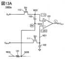
半導体装置100Dは、過電流検知回路として機能する。図10および図11を用いて、半導体装置100Dの動作例について説明する。図10および図11は、半導体装置100Dの動作状態を示す図である。前述した通り、本実施の形態では、電位VRを1.1Vとし、電位VRFNを1.25Vとする。[Example of operation of
The
まず、放電開始前に、端子SHにH電位を供給し、端子SHBにL電位を供給する(図10A参照)。すると、トランジスタ112がオン状態になり、ノードND2の電位が1.1Vになる。また、トランジスタ111がオン状態になり、ノードND1の電位が1.25Vになる。よって、コンパレータ101から出力される電位VOUTがL電位になる。First, before starting discharge, an H potential is supplied to the terminal SH, and an L potential is supplied to the terminal SHB (see FIG. 10A). Then, the
また、この時点では、抵抗121に電流が流れていないため、ノードNDAおよびノードNDBの電位は0V(基準電位)である。端子SHにH電位が供給されると、トランジスタ113がオン状態になり、ノードND3の電位は0Vになる。Further, at this point, since no current is flowing through the
次に、端子SHにL電位を供給し、端子SHBにH電位を供給する(図10B参照)。すると、トランジスタ111がオフ状態になり、ノードND1の電位が保持される。同様に、トランジスタ112がオフ状態になり、ノードND2の電位が保持される。また、トランジスタ113もオフ状態になる。Next, the L potential is supplied to the terminal SH, and the H potential is supplied to the terminal SHB (see FIG. 10B). Then, the
次に、放電動作を開始する。放電が始まると、抵抗121に電流ICが流れる(図11A参照)。電流ICはノードNDBからノードNDAに向かって流れるため、放電が始まるとノードNDBの電位は0Vよりも高くなる。よって、ノードND3の電位も0Vより高くなる。Next, a discharge operation is started. When discharge begins, a current IC flows through the resistor 121 (see FIG. 11A). Since current IC flows from node NDB toward node NDA, the potential of node NDB becomes higher than 0V when discharge begins. Therefore, the potential of node ND3 also becomes higher than 0V.
抵抗121の抵抗値を変えることで、半導体装置100Dで検知する過電流の値を変えることができる。抵抗121を可変抵抗にしてもよい。By changing the resistance value of the
図11Aは、抵抗121の抵抗値RDが150Ωの時に、電流ICとして0.8mAが流れている状態を示している。この場合、ノードNDBの電位は0.12Vになる。よって、ノードND3の電位も0.12Vになる。また、ノードND3とノードND2は容量103を介して容量結合している。よって、ノードND2の電位は1.22Vになる。ノードND1の電位はノードND2の電位よりも大きいままである。よって、電位VOUTはL電位のままである。FIG. 11A shows a state in which 0.8 mA is flowing as the current IC when the resistance value RD of the
図11Bは、抵抗121の抵抗値RDが150Ωの時に、電流ICとして1.1mAが流れた時の状態を示している。この場合、ノードNDBの電位は0.165Vになる。よって、ノードND3の電位も0.165Vになる。上記と同様の理由により、ノードND2の電位が1.265Vになる。すると、ノードND1の電位がノードND2の電位よりも小さくなり、電位VOUTがH電位になる。FIG. 11B shows a state when 1.1 mA flows as current IC when the resistance value RD of the
このようにして、放電動作時の過電流を検知することができる。本発明の一態様の半導体装置100Dは、端子202、トランジスタ213、およびトランジスタ214と直列に接続された抵抗121で過電流の検知を行なう構成である。よって、トランジスタ213およびトランジスタ214の抵抗値ばらつきの影響を受けることなく、精度よく過電流を検知することができる。In this way, overcurrent during discharge operation can be detected. A
<変形例>
図12に、半導体装置200Bの変形例である半導体装置200Baの構成例を示す。本実施の形態では、説明の繰り返しを減らすため、半導体装置200Bと異なる点について主に説明する。半導体装置200Baは、半導体装置100Dに換えて半導体装置100Daを有する点が半導体装置200Bと異なる。<Modified example>
FIG. 12 shows a configuration example of a semiconductor device 200Ba, which is a modification of the
半導体装置100Daは、半導体装置100Dからトランジスタ113、トランジスタ114、端子SHBを除いた構成を有する。半導体装置100Daにおいて、容量103の他方の電極は、抵抗121の他方の端子と電気的に接続する。よって、半導体装置200Baでは、容量103の他方の電極と抵抗121の他方の端子が電気的に接続する節点をノードNDBという。また、半導体装置200Baでは、トランジスタ214のソースまたはドレインの他方と抵抗121の一方の端子が電気的に接続する節点をノードNDAという。The semiconductor device 100Da has a configuration in which the
半導体装置100Daは、半導体装置100Dよりも構成要素が少ないため、占有面積を小さくすることができる。また、半導体装置100Daは端子SHBを有さないため、半導体装置200Baが有する制御回路210から端子227を削減できる。Since the semiconductor device 100Da has fewer components than the
〔半導体装置100Daの動作例〕
半導体装置100Daは、半導体装置100Dと同様に過電流検知回路として機能する。図13および図14を用いて、半導体装置100Daの動作例について説明する。図13および図14は、半導体装置100Daの動作状態を示す図である。[Operation example of semiconductor device 100Da]
The semiconductor device 100Da functions as an overcurrent detection circuit similarly to the
まず、放電開始前に、端子SHにH電位を供給する(図13A参照)。すると、トランジスタ112がオン状態になり、ノードND2の電位が1.1Vになる。また、トランジスタ111がオン状態になり、ノードND1の電位が1.25Vになる。よって、コンパレータ101から出力される電位VOUTがL電位になる。First, before starting discharge, an H potential is supplied to the terminal SH (see FIG. 13A). Then, the
また、この時点では、抵抗121に電流が流れていないため、ノードNDAおよびノードNDBの電位は0V(基準電位)である。Further, at this point, since no current is flowing through the
次に、端子SHにL電位を供給する(図13B参照)。すると、トランジスタ111がオフ状態になり、ノードND1の電位が保持される。同様に、トランジスタ112がオフ状態になり、ノードND2の電位が保持される。Next, the L potential is supplied to the terminal SH (see FIG. 13B). Then, the
次に、放電動作を開始する。放電が始まると、抵抗121に電流ICが流れる(図14A参照)。電流ICはノードNDBからノードNDAに向かって流れるため、放電が始まるとノードNDBの電位は0Vよりも高くなる。Next, a discharge operation is started. When discharge begins, a current IC flows through the resistor 121 (see FIG. 14A). Since current IC flows from node NDB toward node NDA, the potential of node NDB becomes higher than 0V when discharge begins.
図14Aは、抵抗121の抵抗値RDが150Ωの時に、電流ICとして0.8mAが流れている状態を示している。この場合、ノードNDBの電位は0.12Vになる。よって、ノードND3の電位も0.12Vになる。また、ノードNDBとノードND2は容量103を介して容量結合している。よって、ノードND2の電位は1.22Vになる。ノードND1の電位はノードND2の電位よりも大きいままである。よって、電位VOUTはL電位のままである。FIG. 14A shows a state in which 0.8 mA flows as the current IC when the resistance value RD of the
図14Bは、抵抗121の抵抗値RDが150Ωの時に、電流ICとして1.1mAが流れた時の状態を示している。この場合、ノードNDBの電位は0.165Vになる。上記と同様の理由により、ノードND2の電位が1.265Vになる。すると、ノードND1の電位がノードND2の電位よりも小さくなり、電位VOUTがH電位になる。FIG. 14B shows a state in which 1.1 mA flows as current IC when the resistance value RD of the
このようにして、放電動作時の過電流を検知することができる。本発明の一態様の半導体装置200Baは、半導体装置200Bよりも構成要素が少ないため、占有面積をさらに小さくすることができる。In this way, overcurrent during discharge operation can be detected. The semiconductor device 200Ba of one embodiment of the present invention has fewer components than the
なお、本発明の一態様に係る半導体装置は、本実施の形態に示した回路図に限定して解釈されるものではない。本発明の一態様に係る半導体装置には、本実施の形態に示した回路構成と同等の回路構成を有する場合も含まれる。Note that the semiconductor device according to one embodiment of the present invention is not limited to the circuit diagram shown in this embodiment. The semiconductor device according to one embodiment of the present invention also includes a case where the semiconductor device has a circuit structure equivalent to the circuit structure shown in this embodiment.
本実施の形態は、他の実施の形態などに記載した構成と適宜組み合わせて実施することが可能である。This embodiment mode can be implemented in appropriate combination with the structures described in other embodiment modes.
(実施の形態3)
本実施の形態では、本発明の一態様の半導体装置の他の構成例などについて、図面を用いて説明する。(Embodiment 3)
In this embodiment, other structural examples of a semiconductor device of one embodiment of the present invention will be described with reference to drawings.
<半導体装置200Cの構成例>
図15に半導体装置200Cの構成例を示す。半導体装置200Cは、半導体装置200Aおよび半導体装置200Bの変形例である。よって、説明の繰り返しを減らすため、本実施の形態では半導体装置200Aまたは半導体装置200Bと異なる点について主に説明する。<Example of configuration of
FIG. 15 shows a configuration example of a
半導体装置200Cは、制御回路210に換えて制御回路210Aを有する。また、半導体装置200Cは、半導体装置100Cおよび半導体装置100Dの両方を有する。制御回路210Aは制御回路210の変形例であり、制御回路210と同等の機能に加えて、半導体装置100Cおよび半導体装置100Dを制御する機能を有する。The
制御回路210Aは、端子225として端子225aおよび端子225bを有し、端子226として端子226aおよび端子226bを有し、端子227として端子227aおよび端子227bを有する。The
端子225aは、半導体装置100Cの端子OUTと配線122aを介して電気的に接続される。端子225bは、半導体装置100Dの端子OUTと配線122bを介して電気的に接続される。端子226aは、半導体装置100Cの端子SHと電気的に接続される。端子226bは、半導体装置100Dの端子SHと電気的に接続される。端子227aは、半導体装置100Cの端子SHBと電気的に接続される。端子227bは、半導体装置100Dの端子SHBと電気的に接続される。The terminal 225a is electrically connected to the terminal OUT of the
電位生成回路220は、半導体装置100Cの端子Rおよび半導体装置100Dの端子Rに電位VRを供給する機能と、半導体装置100Cの端子RFNおよび半導体装置100Dの端子RFNに電位VRFNを供給する機能と、を有する。The
制御回路210Aは、半導体装置100Cおよび半導体装置100Dを制御する機能を有する。よって、半導体装置200Cは、充電動作時の過電流を検出する機能と、放電動作時の過電流を検出する機能と、を有する。半導体装置200Cを用いることによって、二次電池300の電池寿命をさらに延ばすことができる。また、二次電池300の信頼性をさらに向上することができる。また、二次電池300の安全性をさらに向上することができる。The
また、図16に示すように、半導体装置200Cでは、半導体装置100Cに用いる抵抗121と、半導体装置100Dに用いる抵抗121を共用することができる。よって、半導体装置200Cの構成要素を低減できる。言い換えると、半導体装置200Cを構成する部品の数を少なくできる。Further, as shown in FIG. 16, the
また、半導体装置200Cでは、半導体装置100Cに換えて半導体装置100Caを用いてもよい。同様に、半導体装置100Dに換えて半導体装置100Daを用いてもよい。半導体装置200Cに、半導体装置100Caおよび半導体装置100Daの一方または双方を用いることで、半導体装置200Cの構成要素をさらに低減できる。言い換えると、半導体装置200Cを構成する部品の数をさらに少なくできる。Further, in the
なお、本発明の一態様に係る半導体装置は、本実施の形態に示した回路図に限定して解釈されるものではない。本発明の一態様に係る半導体装置には、本実施の形態に示した回路構成と同等の回路構成を有する場合も含まれる。Note that the semiconductor device according to one embodiment of the present invention is not limited to the circuit diagram shown in this embodiment. The semiconductor device according to one embodiment of the present invention also includes a case where the semiconductor device has a circuit structure equivalent to the circuit structure shown in this embodiment.
本実施の形態は、他の実施の形態などに記載した構成と適宜組み合わせて実施することが可能である。This embodiment mode can be implemented in appropriate combination with the structures described in other embodiment modes.
(実施の形態4)
本実施の形態では、本発明の一態様の半導体装置の他の構成例などについて、図面を用いて説明する。(Embodiment 4)
In this embodiment, other structural examples of a semiconductor device of one embodiment of the present invention will be described with reference to drawings.
<半導体装置200Adの構成例>
図17に半導体装置200Adの構成例を示す。半導体装置200Adは、半導体装置200Aの変形例である。よって、説明の繰り返しを減らすため、半導体装置200Adの半導体装置200Aと異なる点について主に説明する。<Example of configuration of semiconductor device 200Ad>
FIG. 17 shows a configuration example of a semiconductor device 200Ad. The semiconductor device 200Ad is a modification of the
半導体装置200Adは、半導体装置200Aに保護装置250を付加した構成を有する。保護装置250は、端子VP、端子VN、および端子SIGを有する。端子VPは端子201と電気的に接続され、端子VNは端子202と電気的に接続される。よって、端子VPは二次電池300の正極と電気的に接続され、端子VNは二次電池300の負極と電気的に接続される。また、端子SIGは半導体装置100Cの端子OUTと電気的に接続される。また、端子SIGは制御回路210の端子225と電気的に接続される。The semiconductor device 200Ad has a configuration in which a
〔保護装置250〕
保護装置250は、ESD(Electro Static Discharge)などの高電圧ノイズによる、制御回路210および半導体装置100Cの損傷および誤動作などを防ぎ、半導体装置200Adの信頼性を高める機能を有する。[Protective device 250]
The
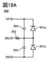
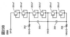
図18Aに保護装置250の等価回路図の一例を示す。図18Aに示す保護装置250は、ダイオード251a、ダイオード251b、抵抗252、および容量253を有する。抵抗252の一方の端子は端子SIGと電気的に接続され、他方の端子はダイオード251aのアノードと電気的に接続される。また、ダイオード251aのカソードは端子VPと電気的に接続される。FIG. 18A shows an example of an equivalent circuit diagram of the
容量253の一方の電極は抵抗252の他方の端子と電気的に接続され、容量253の他方の電極は端子VNと電気的に接続される。ダイオード251bのアノードは端子VNと電気的に接続され、カソードはダイオード251aのアノードと電気的に接続される。すなわち、容量253の一方の電極はダイオード251bのカソードと電気的に接続され、容量253の他方の電極はダイオード251bのアノードと電気的に接続される。容量253とダイオード251bは、並列に接続している。One electrode of
定常状態では、端子VPが高電位側で、端子VNが低電位側であるため、ダイオード251aおよびダイオード251bには逆バイアスが印加される。よって、保護装置250内で端子VPから端子VNへは電流は流れない。しかしながら、ESD現象などによって、予期せず端子VNが端子VPよりも高電位になると、端子VPと端子VNの間が導通状態となり、半導体装置200Adの損傷および誤動作を防ぐことができる。In a steady state, the terminal VP is on the high potential side and the terminal VN is on the low potential side, so a reverse bias is applied to the
また、端子SIGには端子OUTから出力された信号が供給されるが、当該信号は定常状態で端子VNの電位以上、端子VPの電位以下である。よって、定常状態では保護装置250内で端子SIGから端子VPおよび端子VNへは電流は流れない。しかしながら、ESD現象などによって、端子SIGに予期せず端子VPを超える電位もしくは端子VNを下回る電位が印加されると、端子VPまたは端子VNの一方と端子SIGが導通状態となり、半導体装置200Adの損傷および誤動作を防ぐことができる。Further, a signal output from the terminal OUT is supplied to the terminal SIG, and in a steady state, the signal is higher than the potential of the terminal VN and lower than the potential of the terminal VP. Therefore, in the steady state, no current flows from the terminal SIG to the terminals VP and VN within the
また、抵抗252および容量253は直列に接続されており、ハイパスフィルタとして機能する。端子SIGに印加された高周波の高電圧ノイズは、抵抗252および容量253を介して端子VNに逃がされる。Furthermore, the
抵抗252の抵抗値は10Ω以上1kΩ以下が好ましく、50Ω以上500Ω以下がより好ましい。容量253の容量値は0.1pF以上100pF以下が好ましく、1pF以上10pF以下がより好ましい。The resistance value of the
また、図19Aに示すように、抵抗252の他方の端子と端子VPの間に容量254を設けてもよい。容量254の容量値は、容量253と同程度とすればよい。Further, as shown in FIG. 19A, a
また、ダイオード251aおよびダイオード251bは、トランジスタに置き換えることができる。図18Bは、ダイオード251aをトランジスタ251aTに置き換え、ダイオード251bをトランジスタ251bTに置き換えた保護装置250の等価回路図である。トランジスタ251aTのゲートをソースまたはドレインの一方と電気的に接続することで、トランジスタ251aTをダイオードとして機能させることができる。この場合、ゲートと電気的に接続するソースまたはドレインの一方がアノードとして機能し、ソースまたはドレインの他方がカソードとして機能する。Furthermore, the
トランジスタ251aTおよびトランジスタ251bTとして、OSトランジスタを用いることが好ましい。酸化物半導体はバンドギャップが2eV以上あるため、オフ電流が著しく少ないだけでなく、ソースとドレイン間の絶縁耐圧が高い。すなわち、ダイオードで言うところの逆方向電流が少なく、かつ、降伏現象が生じにくい。It is preferable to use OS transistors as the transistor 251aT and the transistor 251bT. Since the oxide semiconductor has a band gap of 2 eV or more, not only the off-state current is extremely small, but also the dielectric strength voltage between the source and the drain is high. That is, the reverse current in a diode is small, and the breakdown phenomenon is less likely to occur.
また、トランジスタ251aTおよびトランジスタ251bTとして、バックゲートを有するトランジスタを用いてもよい。バックゲートを有するトランジスタを用いる場合は、ゲートとバックゲートを電気的に接続すればよい(図18C参照。)。または、バックゲートを端子VNと電気的に接続してもよい(図18D参照。)。Further, a transistor having a back gate may be used as the transistor 251aT and the transistor 251bT. When using a transistor with a back gate, the gate and the back gate may be electrically connected (see FIG. 18C). Alternatively, the back gate may be electrically connected to the terminal VN (see FIG. 18D).
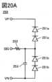
また、図19Bに示すように、複数のダイオード251aを並列に接続してもよい。同様に、複数のダイオード251bを並列に接続してもよい。ダイオード251aおよびダイオード251bを並列に接続することで、保護装置250の電流バイパス能力を高めることができる。また、ダイオード251aおよびダイオード251bの一部が破損しても保護装置250の機能を維持することが出来る。よって、保護装置250の冗長性を高めることができる。Further, as shown in FIG. 19B, a plurality of
また、図20Aに示すように、複数のダイオード251aを直列に接続してもよい。同様に、複数のダイオード251bを直列に接続してもよい。図20Aでは2つのダイオード251aと2つのダイオード251bを直列に接続する例を示している。複数のダイオード251aと複数のダイオード251bをそれぞれ直列に接続することで、ダイオード1つ当たりの逆バイアスが軽減されるため、保護装置250の絶縁耐圧を高めることができる。よって、保護装置250の信頼性を高めることができる。Further, as shown in FIG. 20A, a plurality of
図21Aは、ダイオード251aをトランジスタ251aTに置き換え、ダイオード251bをトランジスタ251bTに置き換えた図20Aに示す保護装置250の等価回路図である。図21Bおよび図21Cは、トランジスタ251aTおよびトランジスタ251bTにバックゲートを有するトランジスタを用いた場合の図20Aに示す保護装置250の等価回路図である。図21Bは、ゲートとバックゲートを電気的に接続する例を示している。図21Cは、バックゲートを端子VNと電気的に接続する例を示している。FIG. 21A is an equivalent circuit diagram of the
また、図20Bに示すように、複数のダイオード251aを直列かつ並列に接続してもよい。同様に、複数のダイオード251bを直列かつ並列に接続してもよい。図20Bでは、直列接続された2つのダイオード251aと、直列接続された2つのダイオード251bが、それぞれ3つ並列接続する例を示している。複数のダイオードを直列かつ並列接続することで、保護装置250の冗長性と絶縁耐圧を高めることができる。よって、保護装置250の信頼性を高めることができる。Further, as shown in FIG. 20B, a plurality of
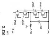
<半導体装置200AdAの構成例>
図22に半導体装置200AdAの構成例を示す。半導体装置200AdAは、半導体装置200Adの変形例である。よって、説明の繰り返しを減らすため、半導体装置200AdAの半導体装置200Adと異なる点について主に説明する。半導体装置200AdAは、半導体装置200Adの保護装置250に換えて保護装置250Aを有する。<Example of configuration of semiconductor device 200AdA>
FIG. 22 shows a configuration example of the semiconductor device 200AdA. The semiconductor device 200AdA is a modification of the semiconductor device 200Ad. Therefore, in order to reduce repetition of the explanation, the differences between the semiconductor device 200AdA and the semiconductor device 200Ad will be mainly explained. The semiconductor device 200AdA has a
また、例えば、制御回路210および/または半導体装置100Cが、バックゲートを有するトランジスタで構成され、当該バックゲートに負極の電位よりも低い電位を供給する場合がある。このような場合は、保護装置250に換えて保護装置250Aを用いればよい。Further, for example, the
図23Aは、保護装置250Aの等価回路図である。図23Aに示す保護装置250Aは、図20Aに示す保護装置250に、2つのダイオード251cと、容量255と、抵抗256と、を有する。容量255の一方の電極は端子VNと電気的に接続され、他方の電極は1つ目のダイオード251cのアノードと電気的に接続される。1つ目のダイオード251cのカソードは、2つ目のダイオード251cのアノードと電気的に接続される。2つ目のダイオード251cのカソードは、端子VNと電気的に接続される。抵抗256の一方の端子は端子VBGと電気的に接続され、他方の端子は1つ目のダイオード251cのアノードと電気的に接続される。端子VBGは、例えば、制御回路210および/または半導体装置100Cに含まれるトランジスタのバックゲートと電気的に接続される。FIG. 23A is an equivalent circuit diagram of the
図23Aでは、ダイオード251a、ダイオード251b、およびダイオード251cをそれぞれ2つずつ直列に接続する構成を示しているが、それぞれ3つ以上の直列であってもよい。ダイオード251a、ダイオード251b、およびダイオード251cをそれぞれ1つで構成してもよい。Although FIG. 23A shows a configuration in which two
図23Bおよび図23Cは、ダイオード251aをトランジスタ251aTに置き換え、ダイオード251bをトランジスタ251bTに置き換え、ダイオード251cをトランジスタ251cTに置き換えた保護装置250Aの等価回路図である。図23Bおよび図23Cでは、トランジスタ251aT、トランジスタ251bT、およびトランジスタ251cTを、バックゲートを有するトランジスタで示しているが、これらのトランジスタはバックゲートを有さないトランジスタであってもよい。図23Bは、ゲートとバックゲートを電気的に接続する例を示している。図23Cは、バックゲートを端子VNと電気的に接続する例を示している。23B and 23C are equivalent circuit diagrams of a
<半導体装置200AdBの構成例>
図24に半導体装置200AdBの構成例を示す。半導体装置200AdBは、半導体装置200Adの変形例である。よって、説明の繰り返しを減らすため、半導体装置200AdBの半導体装置200Adと異なる点について主に説明する。半導体装置200AdBは、半導体装置200Adの保護装置250に換えて保護装置250Bを有する。<Example of configuration of semiconductor device 200AdB>
FIG. 24 shows a configuration example of a semiconductor device 200AdB. The semiconductor device 200AdB is a modification of the semiconductor device 200Ad. Therefore, in order to reduce repetition of explanation, the differences between the semiconductor device 200AdB and the semiconductor device 200Ad will be mainly explained. The semiconductor device 200AdB includes a
保護装置250Bは、保護装置250の変形例である。保護装置250Bは、保護装置250の端子SIGに換えて、端子SIG_inおよび端子SIG_outを有する。端子SIG_inは半導体装置100Cの端子OUTと電気的に接続される。端子SIG_outは配線122を介して端子225と電気的に接続される。
〔保護装置250B〕
図25に保護装置250Bの等価回路図の一例を示す。保護装置250Bは、図18Aに示す保護装置250に抵抗262を付加した構成を有する。抵抗262の一方の端子は抵抗252の他方の端子と電気的に接続され、抵抗262の他方の端子は端子SIG_outと電気的に接続される。[
FIG. 25 shows an example of an equivalent circuit diagram of the
抵抗262の抵抗値は、抵抗252と同様に設定すればよい。端子OUTから出力された信号は、保護装置250Bを通ってから端子225に供給される。このように、信号経路の途中に保護装置を設けてもよい。The resistance value of the
<半導体装置200Bdの構成例>
図26に半導体装置200Bdの構成例を示す。半導体装置200Bdは、半導体装置200Adの変形例である。また、半導体装置200Bdは、半導体装置200Bの変形例でもある。よって、説明の繰り返しを減らすため、半導体装置200Bdの半導体装置200Adと異なる点について主に説明する。同様に、半導体装置200Bdの半導体装置200Bと異なる点について主に説明する。<Example of configuration of semiconductor device 200Bd>
FIG. 26 shows a configuration example of a semiconductor device 200Bd. The semiconductor device 200Bd is a modification of the semiconductor device 200Ad. Further, the semiconductor device 200Bd is also a modification of the
半導体装置200Bdは、半導体装置200Adの半導体装置100Cに換えて半導体装置100Dを有する。よって、端子SIGは半導体装置100Dの端子OUTと電気的に接続される。The semiconductor device 200Bd has a
半導体装置200Bdの構成などについては、半導体装置200Adおよび半導体装置200Bを参酌すれば理解できる。よって、ここでの詳細な説明は省略する。The configuration of the semiconductor device 200Bd can be understood by considering the semiconductor device 200Ad and the
<半導体装置200Cdの構成例>
図27に半導体装置200Cdの構成例を示す。半導体装置200Cdは、半導体装置200Adの変形例である。また、半導体装置200Cdは、半導体装置200Cの変形例でもある。よって、説明の繰り返しを減らすため、半導体装置200Cdの半導体装置200Adと異なる点について主に説明する。同様に、半導体装置200Cdの半導体装置200Cと異なる点について主に説明する。<Configuration example of semiconductor device 200Cd>
FIG. 27 shows a configuration example of a semiconductor device 200Cd. The semiconductor device 200Cd is a modification of the semiconductor device 200Ad. Further, the semiconductor device 200Cd is also a modification of the
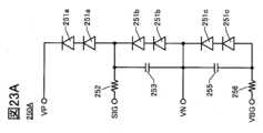
半導体装置200Cdは、半導体装置200Cに保護装置250Cを付加した構成を有する。保護装置250Cは、保護装置250の変形例である。保護装置250Cは、保護装置250の端子SIGに換えて、端子SIG1および端子SIG2を有する。端子SIG1は半導体装置100Cの端子OUTと電気的に接続される。また、端子SIG1は制御回路210Aの端子225aと電気的に接続される。端子SIG2は半導体装置100Dの端子OUTと電気的に接続される。また、端子SIG2は制御回路210Aの端子225bと電気的に接続される。The semiconductor device 200Cd has a configuration in which a
〔保護装置250C〕
図28に保護装置250Cの等価回路図の一例を示す。保護装置250Cは、ダイオード251a_1、ダイオード251b_1、ダイオード251a_2、ダイオード251b_2、抵抗252_1、抵抗252_2、容量253_1、および容量253_2を有する。[
FIG. 28 shows an example of an equivalent circuit diagram of the
抵抗252_1の一方の端子は端子SIG1と電気的に接続され、他方の端子はダイオード251a_1のアノードと電気的に接続される。また、ダイオード251a_1のカソードは端子VPと電気的に接続される。One terminal of the resistor 252_1 is electrically connected to the terminal SIG1, and the other terminal is electrically connected to the anode of the diode 251a_1. Further, the cathode of the diode 251a_1 is electrically connected to the terminal VP.
容量253_1の一方の電極は抵抗252_1の他方の端子と電気的に接続され、容量253_1の他方の電極は端子VNと電気的に接続される。ダイオード251b_1のアノードは端子VNと電気的に接続され、カソードはダイオード251a_1のアノードと電気的に接続される。One electrode of the capacitor 253_1 is electrically connected to the other terminal of the resistor 252_1, and the other electrode of the capacitor 253_1 is electrically connected to the terminal VN. The anode of the diode 251b_1 is electrically connected to the terminal VN, and the cathode is electrically connected to the anode of the diode 251a_1.
抵抗252_2の一方の端子は端子SIG2と電気的に接続され、他方の端子はダイオード251a_2のアノードと電気的に接続される。また、ダイオード251a_2のカソードは端子VPと電気的に接続される。One terminal of the resistor 252_2 is electrically connected to the terminal SIG2, and the other terminal is electrically connected to the anode of the diode 251a_2. Further, the cathode of the diode 251a_2 is electrically connected to the terminal VP.
容量253_2の一方の電極は抵抗252_2の他方の端子と電気的に接続され、容量253_2の他方の電極は端子VNと電気的に接続される。ダイオード251b_1のアノードは端子VNと電気的に接続され、カソードはダイオード251a_2のアノードと電気的に接続される。One electrode of the capacitor 253_2 is electrically connected to the other terminal of the resistor 252_2, and the other electrode of the capacitor 253_2 is electrically connected to the terminal VN. The anode of the diode 251b_1 is electrically connected to the terminal VN, and the cathode is electrically connected to the anode of the diode 251a_2.
保護装置250Cは、実質的に2つの保護装置250を並列に接続した構成を有する。よって、前述した保護装置250の変形例は、保護装置250Cにも適用できる。The
本実施の形態は、他の実施の形態などに記載した構成と適宜組み合わせて実施することが可能である。This embodiment mode can be implemented in appropriate combination with the structures described in other embodiment modes.
(実施の形態5)
本実施の形態では、上記実施の形態で説明した半導体装置に適用可能なトランジスタの構成ついて説明する。具体的には、異なる電気特性を有するトランジスタを積層して設ける構成について説明する。当該構成とすることで、半導体装置の設計自由度を高めることができる。また、異なる電気特性を有するトランジスタを積層して設けることで、半導体装置の集積度を高めることができる。(Embodiment 5)
In this embodiment mode, a structure of a transistor that can be applied to the semiconductor device described in the above embodiment mode will be described. Specifically, a structure in which transistors having different electrical characteristics are stacked will be described. With this configuration, the degree of freedom in designing the semiconductor device can be increased. Further, by stacking and providing transistors having different electrical characteristics, the degree of integration of a semiconductor device can be increased.
図29に示す半導体装置は、トランジスタ400と、トランジスタ500と、容量600と、を有している。図31Aはトランジスタ500のチャネル長方向の断面図であり、図31Bはトランジスタ500のチャネル幅方向の断面図であり、図31Cはトランジスタ400のチャネル幅方向の断面図である。The semiconductor device shown in FIG. 29 includes a
トランジスタ500は、OSトランジスタである。よって、トランジスタ500は、オフ電流が極めて少ないため、これを半導体装置が有するトランジスタに用いることにより、長期にわたり書き込んだデータ電圧あるいは電荷を保持することが可能である。つまり、リフレッシュ動作の頻度が少ない、あるいは、リフレッシュ動作を必要としないため、半導体装置の消費電力を低減することができる。
本実施の形態で説明する半導体装置は、図29に示すようにトランジスタ400、トランジスタ500、容量600を有する。トランジスタ500はトランジスタ400の上方に設けられ、容量600はトランジスタ400、およびトランジスタ500の上方に設けられている。The semiconductor device described in this embodiment includes a
トランジスタ400は、基板311上に設けられ、導電体316、絶縁体315、基板311の一部からなる半導体領域313、ソース領域またはドレイン領域として機能する低抵抗領域314a、および低抵抗領域314bを有する。なお、トランジスタ400は、例えば、上記実施の形態におけるコンパレータ101が有するトランジスタ等に適用することができる。The
トランジスタ400は、図31Cに示すように、半導体領域313の上面およびチャネル幅方向の側面が絶縁体315を介して導電体316に覆われている。このように、トランジスタ400をFin型とすることにより、実効上のチャネル幅が増大することによりトランジスタ400のオン特性を向上させることができる。また、ゲート電極の電界の寄与を高くすることができるため、トランジスタ400のオフ特性を向上させることができる。In the
なお、トランジスタ400は、pチャネル型、あるいはnチャネル型のいずれでもよい。Note that the
半導体領域313のチャネルが形成される領域、その近傍の領域、ソース領域、またはドレイン領域となる低抵抗領域314a、および低抵抗領域314bなどにおいて、シリコン系半導体などの半導体を含むことが好ましく、単結晶シリコンを含むことが好ましい。または、Ge(ゲルマニウム)、SiGe(シリコンゲルマニウム)、GaAs(ガリウムヒ素)、GaAlAs(ガリウムアルミニウムヒ素)などを有する材料で形成してもよい。結晶格子に応力を与え、格子間隔を変化させることで有効質量を制御したシリコンを用いた構成としてもよい。またはGaAsとGaAlAs等を用いることで、トランジスタ400をHEMT(High Electron Mobility Transistor)としてもよい。It is preferable that a semiconductor such as a silicon-based semiconductor be included in the region where a channel is formed in the
低抵抗領域314a、および低抵抗領域314bは、半導体領域313に適用される半導体材料に加え、ヒ素、リンなどのn型の導電性を付与する元素、またはホウ素などのp型の導電性を付与する元素を含む。In addition to the semiconductor material applied to the
ゲート電極として機能する導電体316は、ヒ素、リンなどのn型の導電性を付与する元素、もしくはホウ素などのp型の導電性を付与する元素を含むシリコンなどの半導体材料、金属材料、合金材料、または金属酸化物材料などの導電性材料を用いることができる。The
なお、導電体の材料によって仕事関数が決まるため、当該導電体の材料を選択することで、トランジスタのしきい値電圧を調整することができる。具体的には、導電体に窒化チタンや窒化タンタルなどの材料を用いることが好ましい。さらに導電性と埋め込み性を両立するために導電体にタングステンやアルミニウムなどの金属材料を積層として用いることが好ましく、特にタングステンを用いることが耐熱性の点で好ましい。Note that since the work function is determined by the material of the conductor, the threshold voltage of the transistor can be adjusted by selecting the material of the conductor. Specifically, it is preferable to use a material such as titanium nitride or tantalum nitride for the conductor. Furthermore, in order to achieve both conductivity and embeddability, it is preferable to use a metal material such as tungsten or aluminum as a layered conductor, and it is particularly preferable to use tungsten in terms of heat resistance.
なお、図29に示すトランジスタ400は一例であり、その構造に限定されず、回路構成や駆動方法に応じて適切なトランジスタを用いればよい。例えば、半導体装置をOSトランジスタのみの単極性回路(nチャネル型トランジスタのみ、などと同極性のトランジスタを意味する)とする場合、図30に示すとおり、トランジスタ400の構成を、酸化物半導体を用いているトランジスタ500と同様の構成にすればよい。なお、トランジスタ500の詳細については後述する。Note that the
トランジスタ400を覆って、絶縁体320、絶縁体322、絶縁体324、および絶縁体326が順に積層して設けられている。An
絶縁体320、絶縁体322、絶縁体324、および絶縁体326として、例えば、酸化シリコン、酸化窒化シリコン、窒化酸化シリコン、窒化シリコン、酸化アルミニウム、酸化窒化アルミニウム、窒化酸化アルミニウム、窒化アルミニウムなどを用いればよい。As the
なお、本明細書中において、酸化窒化シリコンとは、その組成として窒素よりも酸素の含有量が多い材料を指し、窒化酸化シリコンとは、その組成として、酸素よりも窒素の含有量が多い材料を示す。また、本明細書中において、酸化窒化アルミニウムとは、その組成として窒素よりも酸素の含有量が多い材料を指し、窒化酸化アルミニウムとは、その組成として、酸素よりも窒素の含有量が多い材料を示す。Note that in this specification, silicon oxynitride refers to a material whose composition contains more oxygen than nitrogen, and silicon nitride oxide refers to a material whose composition contains more nitrogen than oxygen. shows. Furthermore, in this specification, aluminum oxynitride refers to a material whose composition contains more oxygen than nitrogen, and aluminum nitride oxide refers to a material whose composition contains more nitrogen than oxygen. shows.
絶縁体322は、その下方に設けられるトランジスタ400などによって生じる段差を平坦化する平坦化膜としての機能を有していてもよい。例えば、絶縁体322の上面は、平坦性を高めるために化学機械研磨(CMP)法等を用いた平坦化処理により平坦化されていてもよい。The
また、絶縁体324には、基板311、またはトランジスタ400などから、トランジスタ500が設けられる領域に、水素や不純物が拡散しないようなバリア性を有する膜を用いることが好ましい。Further, as the
水素に対するバリア性を有する膜の一例として、例えば、CVD法で形成した窒化シリコンを用いることができる。ここで、トランジスタ500等の酸化物半導体を有する半導体素子に、水素が拡散することで、当該半導体素子の特性が低下する場合がある。したがって、トランジスタ500と、トランジスタ400との間に、水素の拡散を抑制する膜を用いることが好ましい。水素の拡散を抑制する膜とは、具体的には、水素の脱離量が少ない膜とする。As an example of a film having barrier properties against hydrogen, silicon nitride formed by a CVD method can be used, for example. Here, when hydrogen diffuses into a semiconductor element including an oxide semiconductor such as the
水素の脱離量は、例えば、昇温脱離ガス分析法(TDS)などを用いて分析することができる。例えば、絶縁体324の水素の脱離量は、TDS分析において、膜の表面温度が50℃から500℃の範囲において、水素原子に換算した脱離量が、絶縁体324の面積当たりに換算して、10×1015atoms/cm2以下、好ましくは5×1015atoms/cm2以下であればよい。The amount of hydrogen desorbed can be analyzed using, for example, temperature programmed desorption gas analysis (TDS). For example, in TDS analysis, the amount of hydrogen desorbed from the
なお、絶縁体326は、絶縁体324よりも誘電率が低いことが好ましい。例えば、絶縁体326の比誘電率は4未満が好ましく、3未満がより好ましい。また例えば、絶縁体326の比誘電率は、絶縁体324の比誘電率の0.7倍以下が好ましく、0.6倍以下がより好ましい。誘電率が低い材料を層間膜とすることで、配線間に生じる寄生容量を低減することができる。Note that the
また、絶縁体320、絶縁体322、絶縁体324、および絶縁体326には容量600、またはトランジスタ500と接続する導電体328、および導電体330等が埋め込まれている。なお、導電体328、および導電体330は、プラグまたは配線としての機能を有する。また、プラグまたは配線としての機能を有する導電体は、複数の構造をまとめて同一の符号を付与する場合がある。また、本明細書等において、配線と、配線と接続するプラグとが一体物であってもよい。すなわち、導電体の一部が配線として機能する場合、および導電体の一部がプラグとして機能する場合もある。Further, a
各プラグ、および配線(導電体328、導電体330等)の材料としては、金属材料、合金材料、金属窒化物材料、または金属酸化物材料などの導電性材料を、単層または積層して用いることができる。耐熱性と導電性を両立するタングステンやモリブデンなどの高融点材料を用いることが好ましく、タングステンを用いることが好ましい。または、アルミニウムや銅などの低抵抗導電性材料で形成することが好ましい。低抵抗導電性材料を用いることで配線抵抗を低くすることができる。As the material for each plug and the wiring (
絶縁体326、および導電体330上に、配線層を設けてもよい。例えば、図29において、絶縁体350、絶縁体352、および絶縁体354が順に積層して設けられている。また、絶縁体350、絶縁体352、および絶縁体354には、導電体356が形成されている。導電体356は、トランジスタ400と接続するプラグ、または配線としての機能を有する。なお導電体356は、導電体328、および導電体330と同様の材料を用いて設けることができる。A wiring layer may be provided over the
なお、例えば、絶縁体350は、絶縁体324と同様に、水素に対するバリア性を有する絶縁体を用いることが好ましい。また、導電体356は、水素に対するバリア性を有する導電体を含むことが好ましい。特に、水素に対するバリア性を有する絶縁体350が有する開口部に、水素に対するバリア性を有する導電体が形成される。当該構成により、トランジスタ400とトランジスタ500とは、バリア層により分離することができ、トランジスタ400からトランジスタ500への水素の拡散を抑制することができる。Note that, for example, as with the
なお、水素に対するバリア性を有する導電体としては、例えば、窒化タンタル等を用いるとよい。また、窒化タンタルと導電性が高いタングステンを積層することで、配線としての導電性を保持したまま、トランジスタ400からの水素の拡散を抑制することができる。この場合、水素に対するバリア性を有する窒化タンタル層が、水素に対するバリア性を有する絶縁体350と接する構造であることが好ましい。Note that as the conductor having barrier properties against hydrogen, for example, tantalum nitride or the like may be used. Further, by stacking tantalum nitride and highly conductive tungsten, diffusion of hydrogen from the
絶縁体354、および導電体356上に、配線層を設けてもよい。例えば、図29において、絶縁体360、絶縁体362、および絶縁体364が順に積層して設けられている。また、絶縁体360、絶縁体362、および絶縁体364には、導電体366が形成されている。導電体366は、プラグまたは配線としての機能を有する。なお導電体366は、導電体328、および導電体330と同様の材料を用いて設けることができる。A wiring layer may be provided over the
なお、例えば、絶縁体360は、絶縁体324と同様に、水素に対するバリア性を有する絶縁体を用いることが好ましい。また、導電体366は、水素に対するバリア性を有する導電体を含むことが好ましい。特に、水素に対するバリア性を有する絶縁体360が有する開口部に、水素に対するバリア性を有する導電体が形成される。当該構成により、トランジスタ400とトランジスタ500とは、バリア層により分離することができ、トランジスタ400からトランジスタ500への水素の拡散を抑制することができる。Note that, for example, as with the
絶縁体364、および導電体366上に、配線層を設けてもよい。例えば、図29において、絶縁体370、絶縁体372、および絶縁体374が順に積層して設けられている。また、絶縁体370、絶縁体372、および絶縁体374には、導電体376が形成されている。導電体376は、プラグまたは配線としての機能を有する。なお導電体376は、導電体328、および導電体330と同様の材料を用いて設けることができる。A wiring layer may be provided over the
なお、例えば、絶縁体370は、絶縁体324と同様に、水素に対するバリア性を有する絶縁体を用いることが好ましい。また、導電体376は、水素に対するバリア性を有する導電体を含むことが好ましい。特に、水素に対するバリア性を有する絶縁体370が有する開口部に、水素に対するバリア性を有する導電体が形成される。当該構成により、トランジスタ400とトランジスタ500とは、バリア層により分離することができ、トランジスタ400からトランジスタ500への水素の拡散を抑制することができる。Note that, for example, as with the
絶縁体374、および導電体376上に、配線層を設けてもよい。例えば、図29において、絶縁体380、絶縁体382、および絶縁体384が順に積層して設けられている。また、絶縁体380、絶縁体382、および絶縁体384には、導電体386が形成されている。導電体386は、プラグまたは配線としての機能を有する。なお導電体386は、導電体328、および導電体330と同様の材料を用いて設けることができる。A wiring layer may be provided over the
なお、例えば、絶縁体380は、絶縁体324と同様に、水素に対するバリア性を有する絶縁体を用いることが好ましい。また、導電体386は、水素に対するバリア性を有する導電体を含むことが好ましい。特に、水素に対するバリア性を有する絶縁体380が有する開口部に、水素に対するバリア性を有する導電体が形成される。当該構成により、トランジスタ400とトランジスタ500とは、バリア層により分離することができ、トランジスタ400からトランジスタ500への水素の拡散を抑制することができる。Note that, for example, as with the
上記において、導電体356を含む配線層、導電体366を含む配線層、導電体376を含む配線層、および導電体386を含む配線層、について説明したが、本実施の形態に係る半導体装置はこれに限られるものではない。導電体356を含む配線層と同様の配線層を3層以下にしてもよいし、導電体356を含む配線層と同様の配線層を5層以上にしてもよい。In the above, the wiring layer including the
絶縁体384上には絶縁体510、絶縁体512、絶縁体514、および絶縁体516が、順に積層して設けられている。絶縁体510、絶縁体512、絶縁体514、および絶縁体516のいずれかは、酸素や水素に対してバリア性のある物質を用いることが好ましい。An
例えば、絶縁体510、および絶縁体514には、例えば、基板311、またはトランジスタ400を設ける領域などから、トランジスタ500を設ける領域に、水素や不純物が拡散しないようなバリア性を有する膜を用いることが好ましい。したがって、絶縁体324と同様の材料を用いることができる。For example, for the
水素に対するバリア性を有する膜の一例として、CVD法で形成した窒化シリコンを用いることができる。ここで、トランジスタ500等の酸化物半導体を有する半導体素子に、水素が拡散することで、当該半導体素子の特性が低下する場合がある。したがって、トランジスタ500と、トランジスタ400との間に、水素の拡散を抑制する膜を用いることが好ましい。水素の拡散を抑制する膜とは、具体的には、水素の脱離量が少ない膜とする。As an example of a film having barrier properties against hydrogen, silicon nitride formed by a CVD method can be used. Here, when hydrogen diffuses into a semiconductor element including an oxide semiconductor such as the
また、水素に対するバリア性を有する膜として、例えば、絶縁体510、および絶縁体514には、酸化アルミニウム、酸化ハフニウム、酸化タンタルなどの金属酸化物を用いることが好ましい。Further, as a film having barrier properties against hydrogen, for example, it is preferable to use a metal oxide such as aluminum oxide, hafnium oxide, or tantalum oxide for the
特に、酸化アルミニウムは、酸素、およびトランジスタの電気特性の変動要因となる水素、水分などの不純物、の両方に対して膜を透過させない遮断効果が高い。したがって、酸化アルミニウムは、トランジスタの作製工程中および作製後において、水素、水分などの不純物のトランジスタ500への混入を防止することができる。また、トランジスタ500を構成する酸化物からの酸素の放出を抑制することができる。そのため、トランジスタ500に対する保護膜として用いることに適している。In particular, aluminum oxide has a high blocking effect that prevents the membrane from permeating both oxygen and impurities such as hydrogen and moisture that cause fluctuations in the electrical characteristics of the transistor. Therefore, aluminum oxide can prevent impurities such as hydrogen and moisture from entering the
また、例えば、絶縁体512、および絶縁体516には、絶縁体320と同様の材料を用いることができる。また、これらの絶縁体に、比較的誘電率が低い材料を適用することで、配線間に生じる寄生容量を低減することができる。例えば、絶縁体512、および絶縁体516として、酸化シリコン膜や酸化窒化シリコン膜などを用いることができる。Further, for example, the same material as the
また、絶縁体510、絶縁体512、絶縁体514、および絶縁体516には、導電体518、およびトランジスタ500を構成する導電体(例えば、導電体503)等が埋め込まれている。なお、導電体518は、容量600、またはトランジスタ400と接続するプラグ、または配線としての機能を有する。導電体518は、導電体328、および導電体330と同様の材料を用いて設けることができる。Further, a
特に、絶縁体510、および絶縁体514と接する領域の導電体518は、酸素、水素、および水に対するバリア性を有する導電体であることが好ましい。当該構成により、トランジスタ400とトランジスタ500とは、酸素、水素、および水に対するバリア性を有する層で、分離することができ、トランジスタ400からトランジスタ500への水素の拡散を抑制することができる。In particular, the
絶縁体516の上方には、トランジスタ500が設けられている。A
図31Aおよび図31Bに示すように、トランジスタ500は、絶縁体514および絶縁体516に埋め込まれるように配置された導電体503と、絶縁体516および導電体503の上に配置された絶縁体520と、絶縁体520の上に配置された絶縁体522と、絶縁体522の上に配置された絶縁体524と、絶縁体524の上に配置された酸化物530aと、酸化物530aの上に配置された酸化物530bと、酸化物530b上に互いに離れて配置された導電体542aおよび導電体542bと、導電体542aおよび導電体542b上に配置され、導電体542aと導電体542bの間に重畳して開口が形成された絶縁体580と、開口の底面および側面に配置された酸化物530cと、酸化物530cの形成面に配置された絶縁体550と、絶縁体550の形成面に配置された導電体560と、を有する。As shown in FIGS. 31A and 31B, the
また、図31Aおよび図31Bに示すように、酸化物530a、酸化物530b、導電体542a、および導電体542bと、絶縁体580との間に絶縁体544が配置されることが好ましい。また、図31Aおよび図31Bに示すように、導電体560は、絶縁体550の内側に設けられた導電体560aと、導電体560aの内側に埋め込まれるように設けられた導電体560bと、を有することが好ましい。また、図31Aおよび図31Bに示すように、絶縁体580、導電体560、および絶縁体550の上に絶縁体574が配置されることが好ましい。Further, as shown in FIGS. 31A and 31B, an
なお、本明細書等において、酸化物530a、酸化物530b、および酸化物530cをまとめて酸化物530という場合がある。Note that in this specification and the like, the
なお、トランジスタ500では、チャネルが形成される領域と、その近傍において、酸化物530a、酸化物530b、および酸化物530cの3層を積層する構成について示しているが、本発明はこれに限られるものではない。例えば、酸化物530bの単層、酸化物530bと酸化物530aの2層構造、酸化物530bと酸化物530cの2層構造、または4層以上の積層構造を設ける構成にしてもよい。また、トランジスタ500では、導電体560を2層の積層構造として示しているが、本発明はこれに限られるものではない。例えば、導電体560が、単層構造であってもよいし、3層以上の積層構造であってもよい。また、図29、図31Aに示すトランジスタ500は一例であり、その構造に限定されず、回路構成や駆動方法に応じて適切なトランジスタを用いればよい。Note that although the
ここで、導電体560は、トランジスタのゲート電極として機能し、導電体542aおよび導電体542bは、それぞれソース電極またはドレイン電極として機能する。上記のように、導電体560は、絶縁体580の開口、および導電体542aと導電体542bに挟まれた領域に埋め込まれるように形成される。導電体560、導電体542aおよび導電体542bの配置は、絶縁体580の開口に対して、自己整合的に選択される。つまり、トランジスタ500において、ゲート電極を、ソース電極とドレイン電極の間に、自己整合的に配置させることができる。よって、導電体560を位置合わせのマージンを設けることなく形成することができるので、トランジスタ500の占有面積の縮小を図ることができる。これにより、半導体装置の微細化、高集積化を図ることができる。Here, the
さらに、導電体560が、導電体542aと導電体542bの間の領域に自己整合的に形成されるので、導電体560は、導電体542aまたは導電体542bと重畳する領域を有さない。これにより、導電体560と導電体542aおよび導電体542bとの間に形成される寄生容量を低減することができる。よって、トランジスタ500のスイッチング速度を向上させ、高い周波数特性を有せしめることができる。Furthermore, since the
導電体560は、第1のゲート(トップゲートともいう)電極として機能する場合がある。また、導電体503は、第2のゲート(ボトムゲートともいう)電極として機能する場合がある。その場合、導電体503に印加する電位を、導電体560に印加する電位と、連動させず、独立して変化させることで、トランジスタ500のしきい値電圧を制御することができる。特に、導電体503に負の電位を印加することにより、トランジスタ500のしきい値電圧を0Vより大きくし、オフ電流を低減することが可能となる。したがって、導電体503に負の電位を印加したほうが、印加しない場合よりも、導電体560に印加する電位が0Vのときのドレイン電流を小さくすることができる。The
導電体503は、酸化物530、および導電体560と、重なるように配置する。これにより、導電体560、および導電体503に電位を印加した場合、導電体560から生じる電界と、導電体503から生じる電界と、がつながり、酸化物530に形成されるチャネル形成領域を覆うことができる。The
本明細書等において、一対のゲート電極(第1のゲート電極、および第2のゲート電極)の電界によって、チャネル形成領域を電気的に取り囲むトランジスタの構造を、surrounded channel(S-channel)構造とよぶ。また、本明細書等において、surrounded channel(S-channel)構造は、ソース電極およびドレイン電極として機能する導電体542aおよび導電体542bに接する酸化物530の側面および周辺が、チャネル形成領域と同じくI型であるといった特徴を有する。また、導電体542aおよび導電体542bに接する酸化物530の側面および周辺は、絶縁体544と接しているため、チャネル形成領域と同様にI型となりうる。なお、本明細書等において、I型とは後述する、高純度真性と同様として扱うことができる。また、本明細書等で開示するS-channel構造は、Fin型構造およびプレーナ型構造とは異なる。S-channel構造を採用することで、短チャネル効果に対する耐性を高める、別言すると短チャネル効果が発生し難いトランジスタとすることができる。In this specification and the like, a structure of a transistor in which a channel formation region is electrically surrounded by an electric field of a pair of gate electrodes (a first gate electrode and a second gate electrode) is referred to as a surrounded channel (S-channel) structure. Call me. Further, in this specification and the like, in a surrounded channel (S-channel) structure, the side surfaces and periphery of the
また、導電体503は、導電体518と同様の構成であり、絶縁体514および絶縁体516の開口の内壁に接して導電体503aが形成され、さらに内側に導電体503bが形成されている。なお、トランジスタ500では、導電体503aおよび導電体503bを積層する構成について示しているが、本発明はこれに限られるものではない。例えば、導電体503は、単層、または3層以上の積層構造として設ける構成にしてもよい。Further, the
ここで、導電体503aは、水素原子、水素分子、水分子、銅原子などの不純物の拡散を抑制する機能を有する(上記不純物が透過しにくい。)導電性材料を用いることが好ましい。または、酸素(例えば、酸素原子、酸素分子などの少なくとも一)の拡散を抑制する機能を有する(上記酸素が透過しにくい。)導電性材料を用いることが好ましい。なお、本明細書において、不純物、または酸素の拡散を抑制する機能とは、上記不純物、または上記酸素のいずれか一または、すべての拡散を抑制する機能とする。Here, as the
例えば、導電体503aが酸素の拡散を抑制する機能を持つことにより、導電体503bが酸化して導電率が低下することを抑制することができる。For example, when the
また、導電体503が配線の機能を兼ねる場合、導電体503bは、タングステン、銅、またはアルミニウムを主成分とする、導電性が高い導電性材料を用いることが好ましい。なお、本実施の形態では導電体503を導電体503aと導電体503bの積層で図示したが、導電体503は単層構造であってもよい。Further, in the case where the
絶縁体520、絶縁体522、および絶縁体524は、第2のゲート絶縁膜としての機能を有する。The
ここで、酸化物530と接する絶縁体524は、化学量論的組成を満たす酸素よりも多くの酸素を含む絶縁体を用いることが好ましい。つまり、絶縁体524には、過剰酸素領域が形成されていることが好ましい。このような過剰酸素を含む絶縁体を酸化物530に接して設けることにより、酸化物530中の酸素欠損(VO:oxygen vacancyともいう)を低減し、トランジスタ500の信頼性を向上させることができる。なお、酸化物530中の酸素欠損に水素が入った場合、当該欠陥(以下、VOHと呼ぶ場合がある。)はドナーとして機能し、キャリアである電子が生成されることがある。また、水素の一部が金属原子と結合する酸素と結合して、キャリアである電子を生成する場合がある。従って、水素が多く含まれている酸化物半導体を用いたトランジスタは、ノーマリーオン特性となりやすい。また、酸化物半導体中の水素は、熱、電界などのストレスによって動きやすいため、酸化物半導体に多くの水素が含まれると、トランジスタの信頼性が悪化する恐れもある。本発明の一態様においては、酸化物530中のVOHをできる限り低減し、高純度真性または実質的に高純度真性にすることが好ましい。このように、VOHが十分低減された酸化物半導体を得るには、酸化物半導体中の水分、水素などの不純物を除去すること(脱水、脱水素化処理と記載する場合がある。)と、酸化物半導体に酸素を供給して酸素欠損を補填すること(加酸素化処理と記載する場合がある。)が重要である。VOHなどの不純物が十分に低減された酸化物半導体をトランジスタのチャネル形成領域に用いることで、安定した電気特性を付与することができる。Here, as the
過剰酸素領域を有する絶縁体として、具体的には、加熱により一部の酸素が脱離する酸化物材料を用いることが好ましい。加熱により酸素を脱離する酸化物とは、TDS(Thermal Desorption Spectroscopy)分析にて、酸素原子に換算しての酸素の脱離量が1.0×10¹⁸atoms/cm3以上、好ましくは1.0×1019atoms/cm3以上、さらに好ましくは2.0×1019atoms/cm3以上、または3.0×1020atoms/cm3以上である酸化物膜である。なお、上記TDS分析時における膜の表面温度としては100℃以上700℃以下、または100℃以上400℃以下の範囲が好ましい。Specifically, as the insulator having an excess oxygen region, it is preferable to use an oxide material from which some oxygen is released by heating. An oxide that desorbs oxygen by heating is an oxide with an amount of desorbed oxygen in terms of oxygen atoms of 1.0×10¹⁸ atoms/cm3 or more, preferably 1 in TDS (Thermal Desorption Spectroscopy) analysis. The oxide film has a density of .0×1019 atoms/cm3 or more, more preferably 2.0×10¹⁹ atoms/cm3 or more, or 3.0×10²⁰ atoms/cm3 or more. Note that the surface temperature of the film during the above TDS analysis is preferably in the range of 100°C or more and 700°C or less, or 100°C or more and 400°C or less.
また、上記過剰酸素領域を有する絶縁体と、酸化物530と、を接して加熱処理、マイクロ波処理、またはRF処理のいずれか一または複数の処理を行っても良い。当該処理を行うことで、酸化物530中の水、または水素を除去することができる。例えば、酸化物530において、VoHの結合が切断される反応が起きる、別言すると「VOH→Vo+H」という反応が起きて、脱水素化することができる。このとき発生した水素の一部は、酸素と結合してH2Oとして、酸化物530、または酸化物530近傍の絶縁体から除去される場合がある。また、水素の一部は、導電体542にゲッタリングされる場合がある。Further, the insulator having the excess oxygen region and the
また、上記マイクロ波処理は、例えば、高密度プラズマを発生させる電源を有する装置、または、基板側にRFを印加する電源を有する装置を用いると好適である。例えば、酸素を含むガスを用い、且つ高密度プラズマを用いることより、高密度の酸素ラジカルを生成することができ、基板側にRFを印加することで、高密度プラズマによって生成された酸素ラジカルを、効率よく酸化物530、または酸化物530近傍の絶縁体中に導入することができる。また、上記マイクロ波処理は、圧力を133Pa以上、好ましくは200Pa以上、さらに好ましくは400Pa以上とすればよい。また、マイクロ波処理を行う装置内に導入するガスとしては、例えば、酸素と、アルゴンとを用い、酸素流量比(O2/(O2+Ar))が50%以下、好ましくは10%以上30%以下で行うとよい。Further, for the microwave processing, it is preferable to use, for example, an apparatus having a power source for generating high-density plasma or an apparatus having a power source for applying RF to the substrate side. For example, by using a gas containing oxygen and using high-density plasma, high-density oxygen radicals can be generated, and by applying RF to the substrate side, the oxygen radicals generated by the high-density plasma can be generated. , can be efficiently introduced into the
また、トランジスタ500の作製工程中において、酸化物530の表面が露出した状態で、加熱処理を行うと好適である。当該加熱処理は、例えば、100℃以上450℃以下、より好ましくは350℃以上400℃以下で行えばよい。なお、加熱処理は、窒素ガスもしくは不活性ガスの雰囲気、または酸化性ガスを10ppm以上、1%以上、もしくは10%以上含む雰囲気で行う。例えば、加熱処理は酸素雰囲気で行うことが好ましい。これにより、酸化物530に酸素を供給して、酸素欠損(VO)の低減を図ることができる。また、加熱処理は減圧状態で行ってもよい。または、加熱処理は、窒素ガスもしくは不活性ガスの雰囲気で加熱処理した後に、脱離した酸素を補うために、酸化性ガスを10ppm以上、1%以上、または10%以上含む雰囲気で行ってもよい。または、酸化性ガスを10ppm以上、1%以上、または10%以上含む雰囲気で加熱処理した後に、連続して窒素ガスもしくは不活性ガスの雰囲気で加熱処理を行っても良い。Further, during the manufacturing process of the
なお、酸化物530に加酸素化処理を行うことで、酸化物530中の酸素欠損を、供給された酸素により修復させる、別言すると「Vo+O→null」という反応を促進させることができる。さらに、酸化物530中に残存した水素に供給された酸素が反応することで、当該水素をH2Oとして除去する(脱水化する)ことができる。これにより、酸化物530中に残存していた水素が酸素欠損に再結合してVOHが形成されるのを抑制することができる。Note that by performing the oxygenation treatment on the
また、絶縁体524が、過剰酸素領域を有する場合、絶縁体522は、酸素(例えば、酸素原子、酸素分子など)の拡散を抑制する機能を有する(上記酸素が透過しにくい)ことが好ましい。Further, when the
絶縁体522が、酸素や不純物の拡散を抑制する機能を有することで、酸化物530が有する酸素は、絶縁体520側へ拡散することがなく、好ましい。また、導電体503が、絶縁体524や、酸化物530が有する酸素と反応することを抑制することができる。Since the
絶縁体522は、例えば、酸化アルミニウム、酸化ハフニウム、アルミニウムおよびハフニウムを含む酸化物(ハフニウムアルミネート)、酸化タンタル、酸化ジルコニウム、チタン酸ジルコン酸鉛(PZT)、チタン酸ストロンチウム(SrTiO3)、または(Ba,Sr)TiO3(BST)などのいわゆるhigh-k材料を含む絶縁体を単層または積層で用いることが好ましい。トランジスタの微細化、および高集積化が進むと、ゲート絶縁膜の薄膜化により、リーク電流などの問題が生じる場合がある。ゲート絶縁膜として機能する絶縁体にhigh-k材料を用いることで、物理膜厚を保ちながら、トランジスタ動作時のゲート電位の低減が可能となる。The
特に、不純物、および酸素などの拡散を抑制する機能を有する(上記酸素が透過しにくい)絶縁性材料であるアルミニウム、ハフニウムの一方または双方の酸化物を含む絶縁体を用いるとよい。アルミニウム、ハフニウムの一方または双方の酸化物を含む絶縁体として、酸化アルミニウム、酸化ハフニウム、アルミニウムおよびハフニウムを含む酸化物(ハフニウムアルミネート)などを用いることが好ましい。このような材料を用いて絶縁体522を形成した場合、絶縁体522は、酸化物530からの酸素の放出や、トランジスタ500の周辺部から酸化物530への水素等の不純物の混入を抑制する層として機能する。In particular, it is preferable to use an insulator containing an oxide of one or both of aluminum and hafnium, which is an insulating material that has the function of suppressing the diffusion of impurities and oxygen (the above-mentioned oxygen is difficult to permeate). As the insulator containing an oxide of one or both of aluminum and hafnium, it is preferable to use aluminum oxide, hafnium oxide, an oxide containing aluminum and hafnium (hafnium aluminate), and the like. When the
または、これらの絶縁体に、例えば、酸化アルミニウム、酸化ビスマス、酸化ゲルマニウム、酸化ニオブ、酸化シリコン、酸化チタン、酸化タングステン、酸化イットリウム、酸化ジルコニウムを添加してもよい。またはこれらの絶縁体を窒化処理してもよい。上記の絶縁体に酸化シリコン、酸化窒化シリコンまたは窒化シリコンを積層して用いてもよい。Alternatively, aluminum oxide, bismuth oxide, germanium oxide, niobium oxide, silicon oxide, titanium oxide, tungsten oxide, yttrium oxide, or zirconium oxide may be added to these insulators. Alternatively, these insulators may be nitrided. Silicon oxide, silicon oxynitride, or silicon nitride may be stacked on the above insulator.
また、絶縁体520は、熱的に安定していることが好ましい。例えば、酸化シリコンおよび酸化窒化シリコンは、熱的に安定であるため、好適である。また、high-k材料の絶縁体を酸化シリコン、または酸化窒化シリコンと組み合わせることで、熱的に安定かつ比誘電率の高い積層構造の絶縁体520を得ることができる。Further, it is preferable that the
なお、図31Aおよび図31Bのトランジスタ500では、3層の積層構造からなる第2のゲート絶縁膜として、絶縁体520、絶縁体522、および絶縁体524が図示されているが、第2のゲート絶縁膜は、単層、2層、または4層以上の積層構造を有していてもよい。その場合、同じ材料からなる積層構造に限定されず、異なる材料からなる積層構造でもよい。Note that in the
トランジスタ500は、チャネル形成領域を含む酸化物530に、酸化物半導体として機能する金属酸化物を用いることが好ましい。例えば、酸化物530として、In-M-Zn酸化物(元素Mは、アルミニウム、ガリウム、イットリウム、銅、バナジウム、ベリリウム、ホウ素、チタン、鉄、ニッケル、ゲルマニウム、ジルコニウム、モリブデン、ランタン、セリウム、ネオジム、ハフニウム、タンタル、タングステン、またはマグネシウムなどから選ばれた一種、または複数種)等の金属酸化物を用いるとよい。特に、酸化物530として適用できるIn-M-Zn酸化物は、CAAC-OS(c-axis aligned crystalline oxide semiconductor)であることが好ましい。または、CAC-OS(Cloud-Aligned Composite oxide semiconductor)であることが好ましい。なお、CAACは結晶構造の一例を表し、CACは機能、または材料の構成の一例を表す。また、酸化物530として、In-Ga酸化物、In-Zn酸化物を用いてもよい。In the
CAC-OSは、CAC-metal oxideと呼ばれる場合がある。CAC-OSまたはCAC-metal oxideとは、材料の一部では導電性の機能と、材料の一部では絶縁性の機能とを有し、材料の全体では半導体としての機能を有する。なお、CAC-OSまたはCAC-metal oxideを、トランジスタのチャネル形成領域に用いる場合、導電性の機能は、キャリアとなる電子(またはホール)を流す機能であり、絶縁性の機能は、キャリアとなる電子を流さない機能である。導電性の機能と、絶縁性の機能とを、それぞれ相補的に作用させることで、スイッチングさせる機能(On/Offさせる機能)をCAC-OSまたはCAC-metal oxideに付与することができる。CAC-OSまたはCAC-metal oxideにおいて、それぞれの機能を分離させることで、双方の機能を最大限に高めることができる。CAC-OS is sometimes called CAC-metal oxide. CAC-OS or CAC-metal oxide has a part of the material having a conductive function, a part of the material having an insulating function, and the entire material having a semiconductor function. Note that when CAC-OS or CAC-metal oxide is used in the channel formation region of a transistor, the conductive function is the function of flowing electrons (or holes) that become carriers, and the insulating function is the function of flowing electrons (or holes) that become carriers. This function does not allow electrons to flow. A switching function (on/off function) can be imparted to CAC-OS or CAC-metal oxide by making the conductive function and the insulating function act complementary to each other. By separating the functions of CAC-OS or CAC-metal oxide, the functions of both can be maximized.
また、CAC-OSまたはCAC-metal oxideは、導電性領域、及び絶縁性領域を有する。導電性領域は、上述の導電性の機能を有し、絶縁性領域は、上述の絶縁性の機能を有する。また、材料中において、導電性領域と、絶縁性領域とは、ナノ粒子レベルで分離している場合がある。また、導電性領域と、絶縁性領域とは、それぞれ材料中に偏在する場合がある。また、導電性領域は、周辺がぼけてクラウド状に連結して観察される場合がある。Further, CAC-OS or CAC-metal oxide has a conductive region and an insulating region. The conductive region has the above-mentioned conductive function, and the insulating region has the above-mentioned insulating function. Further, in a material, a conductive region and an insulating region may be separated at the nanoparticle level. Further, the conductive region and the insulating region may be unevenly distributed in the material. Further, the conductive regions may be observed to be connected in a cloud-like manner with the periphery blurred.
また、CAC-OSまたはCAC-metal oxideにおいて、導電性領域と、絶縁性領域とは、それぞれ0.5nm以上10nm以下、好ましくは0.5nm以上3nm以下のサイズで材料中に分散している場合がある。Further, in CAC-OS or CAC-metal oxide, when the conductive region and the insulating region are each dispersed in the material with a size of 0.5 nm or more and 10 nm or less, preferably 0.5 nm or more and 3 nm or less. There is.
また、CAC-OSまたはCAC-metal oxideは、異なるバンドギャップを有する成分により構成される。例えば、CAC-OSまたはCAC-metal oxideは、絶縁性領域に起因するワイドギャップを有する成分と、導電性領域に起因するナローギャップを有する成分と、により構成される。当該構成の場合、キャリアを流す際に、ナローギャップを有する成分において、主にキャリアが流れる。また、ナローギャップを有する成分が、ワイドギャップを有する成分に相補的に作用し、ナローギャップを有する成分に連動してワイドギャップを有する成分にもキャリアが流れる。このため、上記CAC-OSまたはCAC-metal oxideをトランジスタのチャネル形成領域に用いる場合、トランジスタのオン状態において高い電流駆動力、つまり大きなオン電流、及び高い電界効果移動度を得ることができる。Further, CAC-OS or CAC-metal oxide is composed of components having different band gaps. For example, CAC-OS or CAC-metal oxide is composed of a component having a wide gap caused by an insulating region and a component having a narrow gap caused by a conductive region. In the case of this configuration, when the carrier flows, the carrier mainly flows in the component having the narrow gap. Furthermore, the component having a narrow gap acts complementary to the component having a wide gap, and carriers also flow into the component having a wide gap in conjunction with the component having a narrow gap. Therefore, when the above-mentioned CAC-OS or CAC-metal oxide is used in the channel formation region of a transistor, a high current driving force, that is, a large on-state current, and high field effect mobility can be obtained in the on state of the transistor.
すなわち、CAC-OSまたはCAC-metal oxideは、マトリックス複合材(matrix composite)、または金属マトリックス複合材(metal matrix composite)と呼称することもできる。That is, CAC-OS or CAC-metal oxide can also be referred to as a matrix composite or a metal matrix composite.
なお、酸化物半導体として機能する金属酸化物は、単結晶酸化物半導体と、それ以外の非単結晶酸化物半導体と、に分けられる。非単結晶酸化物半導体としては、例えば、CAAC-OS、多結晶酸化物半導体、nc-OS(nanocrystalline oxide semiconductor)、擬似非晶質酸化物半導体(a-like OS:amorphous-like oxide semiconductor)、および非晶質酸化物半導体などがある。Note that metal oxides that function as oxide semiconductors are classified into single-crystal oxide semiconductors and other non-single-crystal oxide semiconductors. Examples of non-single crystal oxide semiconductors include CAAC-OS, polycrystalline oxide semiconductor, nc-OS (nanocrystalline oxide semiconductor), and amorphous-like oxide semiconductor (a-like OS). ), and amorphous oxide semiconductors.
CAAC-OSは、c軸配向性を有し、かつa-b面方向において複数のナノ結晶が連結し、歪みを有した結晶構造となっている。なお、歪みとは、複数のナノ結晶が連結する領域において、格子配列の揃った領域と、別の格子配列の揃った領域と、の間で格子配列の向きが変化している箇所を指す。CAAC-OS has c-axis orientation and a plurality of nanocrystals connected in the a-b plane direction, resulting in a distorted crystal structure. Note that distortion refers to a location where the orientation of the lattice arrangement changes between a region where the lattice arrangement is uniform and another region where the lattice arrangement is uniform in a region where a plurality of nanocrystals are connected.
ナノ結晶は、六角形を基本とするが、正六角形状とは限らず、非正六角形状である場合がある。また、歪みにおいて、五角形、および七角形などの格子配列を有する場合がある。なお、CAAC-OSにおいて、歪み近傍においても、明確な結晶粒界(グレインバウンダリーともいう。)を確認することは難しい。すなわち、格子配列の歪みによって、結晶粒界の形成が抑制されていることがわかる。これは、CAAC-OSが、a-b面方向において酸素原子の配列が稠密でないことや、金属元素が置換することで原子間の結合距離が変化することなどによって、歪みを許容することができるためである。Although nanocrystals are basically hexagonal, they are not limited to regular hexagonal shapes and may have irregular hexagonal shapes. In addition, the distortion may have a pentagonal or heptagonal lattice arrangement. Note that in CAAC-OS, it is difficult to confirm clear grain boundaries (also referred to as grain boundaries) even in the vicinity of strain. That is, it can be seen that the formation of grain boundaries is suppressed by the distortion of the lattice arrangement. This is because CAAC-OS can tolerate distortion due to the fact that the arrangement of oxygen atoms is not dense in the a-b plane direction, and the bond distance between atoms changes due to substitution of metal elements. It's for a reason.
また、CAAC-OSは、インジウム、および酸素を有する層(以下、In層)と、元素M、亜鉛、および酸素を有する層(以下、(M,Zn)層)とが積層した、層状の結晶構造(層状構造ともいう)を有する傾向がある。なお、インジウムと元素Mは、互いに置換可能であり、(M,Zn)層の元素Mがインジウムと置換した場合、(In,M,Zn)層と表すこともできる。また、In層のインジウムが元素Mと置換した場合、(In,M)層と表すこともできる。In addition, CAAC-OS is a layered crystal in which a layer containing indium and oxygen (hereinafter referred to as an "In layer") and a layer containing element M, zinc, and oxygen (hereinafter referred to as a (M,Zn) layer) are laminated. They tend to have a structure (also called a layered structure). Note that indium and element M can be substituted with each other, and when element M in a (M, Zn) layer is substituted with indium, it can also be expressed as an (In, M, Zn) layer. Furthermore, when indium in the In layer is replaced with element M, it can also be expressed as an (In, M) layer.
CAAC-OSは結晶性の高い金属酸化物である。一方、CAAC-OSは、明確な結晶粒界を確認することが難しいため、結晶粒界に起因する電子移動度の低下が起こりにくいといえる。また、金属酸化物の結晶性は不純物の混入や欠陥の生成などによって低下する場合があるため、CAAC-OSは不純物や欠陥(酸素欠損など)の少ない金属酸化物ともいえる。したがって、CAAC-OSを有する金属酸化物は、物理的性質が安定する。そのため、CAAC-OSを有する金属酸化物は熱に強く、信頼性が高い。CAAC-OS is a highly crystalline metal oxide. On the other hand, in CAAC-OS, it is difficult to confirm clear grain boundaries, so it can be said that reduction in electron mobility due to grain boundaries is less likely to occur. Further, since the crystallinity of a metal oxide may be reduced due to the incorporation of impurities or the formation of defects, CAAC-OS can also be said to be a metal oxide with few impurities or defects (oxygen vacancies, etc.). Therefore, the metal oxide with CAAC-OS has stable physical properties. Therefore, metal oxides with CAAC-OS are resistant to heat and have high reliability.
nc-OSは、微小な領域(例えば、1nm以上10nm以下の領域、特に1nm以上3nm以下の領域)において原子配列に周期性を有する。また、nc-OSは、異なるナノ結晶間で結晶方位に規則性が見られない。そのため、膜全体で配向性が見られない。したがって、nc-OSは、分析方法によっては、a-like OSや非晶質酸化物半導体と区別が付かない場合がある。The nc-OS has periodicity in the atomic arrangement in a minute region (for example, a region of 1 nm or more and 10 nm or less, particularly a region of 1 nm or more and 3 nm or less). Further, in nc-OS, no regularity is observed in crystal orientation between different nanocrystals. Therefore, no orientation is observed throughout the film. Therefore, depending on the analysis method, nc-OS may be indistinguishable from a-like OS or amorphous oxide semiconductor.
なお、インジウムと、ガリウムと、亜鉛と、を有する金属酸化物の一種である、In-Ga-Zn酸化物(「IGZO」ともいう。)は、上述のナノ結晶とすることで安定な構造をとる場合がある。特に、IGZOは、大気中では結晶成長がし難い傾向があるため、大きな結晶(ここでは、数mmの結晶、または数cmの結晶)よりも小さな結晶(例えば、上述のナノ結晶)とする方が、構造的に安定となる場合がある。Note that In-Ga-Zn oxide (also referred to as "IGZO"), which is a type of metal oxide containing indium, gallium, and zinc, has a stable structure by forming the above-mentioned nanocrystals. It may be taken. In particular, IGZO tends to have difficulty growing crystals in the atmosphere, so it is better to form small crystals (for example, the nanocrystals mentioned above) rather than large crystals (here, crystals of several mm or crystals of several cm). may be structurally stable.
a-like OSは、nc-OSと非晶質酸化物半導体との間の構造を有する金属酸化物である。a-like OSは、鬆または低密度領域を有する。すなわち、a-like OSは、nc-OSおよびCAAC-OSと比べて、結晶性が低い。The a-like OS is a metal oxide with a structure between that of an nc-OS and an amorphous oxide semiconductor. A-like OS has holes or low density areas. That is, a-like OS has lower crystallinity than nc-OS and CAAC-OS.
酸化物半導体(金属酸化物)は、多様な構造をとり、それぞれが異なる特性を有する。本発明の一態様の酸化物半導体は、非晶質酸化物半導体、多結晶酸化物半導体、a-like OS、nc-OS、CAAC-OSのうち、二種以上を有していてもよい。Oxide semiconductors (metal oxides) have a variety of structures, each with different properties. The oxide semiconductor of one embodiment of the present invention may include two or more types of an amorphous oxide semiconductor, a polycrystalline oxide semiconductor, an a-like OS, an nc-OS, and a CAAC-OS.
また、トランジスタ500には、キャリア濃度の低い金属酸化物を用いることが好ましい。金属酸化物のキャリア濃度を低くする場合においては、金属酸化物中の不純物濃度を低くし、欠陥準位密度を低くすればよい。本明細書等において、不純物濃度が低く、欠陥準位密度の低いことを高純度真性または実質的に高純度真性という。なお、金属酸化物中の不純物としては、例えば、水素、窒素、アルカリ金属、アルカリ土類金属、鉄、ニッケル、シリコン等がある。Further, a metal oxide with a low carrier concentration is preferably used for the
特に、金属酸化物に含まれる水素は、金属原子と結合する酸素と反応して水になるため、金属酸化物中に酸素欠損を形成する場合がある。金属酸化物中のチャネル形成領域に酸素欠損が含まれていると、トランジスタはノーマリーオン特性となる場合がある。さらに、酸素欠損に水素が入った欠陥はドナーとして機能し、キャリアである電子が生成されることがある。また、水素の一部が金属原子と結合する酸素と結合して、キャリアである電子を生成する場合がある。従って、水素が多く含まれている金属酸化物を用いたトランジスタは、ノーマリーオン特性となりやすい。In particular, hydrogen contained in metal oxides reacts with oxygen bonded to metal atoms to become water, which may form oxygen vacancies in metal oxides. If oxygen vacancies are included in the channel formation region in the metal oxide, the transistor may exhibit normally-on characteristics. Furthermore, defects in which hydrogen is inserted into oxygen vacancies function as donors, and electrons, which are carriers, may be generated. Further, a portion of hydrogen may combine with oxygen that is bonded to a metal atom to generate electrons, which are carriers. Therefore, a transistor using a metal oxide containing a large amount of hydrogen tends to have normally-on characteristics.
酸素欠損に水素が入った欠陥は、金属酸化物のドナーとして機能しうる。しかしながら、当該欠陥を定量的に評価することは困難である。そこで、金属酸化物においては、ドナー濃度ではなく、キャリア濃度で評価される場合がある。よって、本明細書等では、金属酸化物のパラメータとして、ドナー濃度ではなく、電界が印加されない状態を想定したキャリア濃度を用いる場合がある。つまり、本明細書等に記載の「キャリア濃度」は、「ドナー濃度」と言い換えることができる場合がある。Defects in which hydrogen is inserted into oxygen vacancies can function as donors for metal oxides. However, it is difficult to quantitatively evaluate the defect. Therefore, metal oxides are sometimes evaluated based on carrier concentration instead of donor concentration. Therefore, in this specification and the like, as a parameter of a metal oxide, a carrier concentration assuming a state in which no electric field is applied is sometimes used instead of a donor concentration. That is, the "carrier concentration" described in this specification and the like can sometimes be translated into "donor concentration."
よって、金属酸化物を酸化物530に用いる場合、金属酸化物中の水素はできる限り低減されていることが好ましい。具体的には、金属酸化物において、二次イオン質量分析法(SIMS:Secondary Ion Mass Spectrometry)により得られる水素濃度を、1×10²⁰atoms/cm3未満、好ましくは1×1019atoms/cm3未満、より好ましくは5×1018atoms/cm3未満、さらに好ましくは1×1018atoms/cm3未満とする。水素などの不純物が十分に低減された金属酸化物をトランジスタのチャネル形成領域に用いることで、安定した電気特性を付与することができる。Therefore, when a metal oxide is used as the
また、酸化物530に金属酸化物を用いる場合、チャネル形成領域の金属酸化物のキャリア濃度は、1×1018cm-3以下であることが好ましく、1×1017cm-3未満であることがより好ましく、1×1016cm-3未満であることがさらに好ましく、1×1013cm-3未満であることがさらに好ましく、1×1012cm-3未満であることがさらに好ましい。なお、チャネル形成領域の金属酸化物のキャリア濃度の下限値については、特に限定は無いが、例えば、1×10⁻⁹cm-3とすることができる。Further, when a metal oxide is used as the
また、酸化物530に金属酸化物を用いる場合、導電体542(導電体542a、および導電体542b)と酸化物530とが接することで、酸化物530中の酸素が導電体542へ拡散し、導電体542が酸化する場合がある。導電体542が酸化することで、導電体542の導電率が低下する蓋然性が高い。なお、酸化物530中の酸素が導電体542へ拡散することを、導電体542が酸化物530中の酸素を吸収する、と言い換えることができる。Further, when a metal oxide is used as the
また、酸化物530中の酸素が導電体542(導電体542a、および導電体542b)へ拡散することで、導電体542aと酸化物530bとの間、および、導電体542bと酸化物530bとの間に異層が形成される場合がある。当該異層は、導電体542よりも酸素を多く含むため、当該異層は絶縁性を有すると推定される。このとき、導電体542と、当該異層と、酸化物530bとの3層構造は、金属-絶縁体-半導体からなる3層構造とみなすことができ、MIS(Metal-Insulator-Semiconductor)構造と呼ぶ、またはMIS構造を主としたダイオード接合構造と呼ぶ場合がある。In addition, oxygen in the
なお、上記異層は、導電体542と酸化物530bとの間に形成されることに限られず、例えば、異層が、導電体542と酸化物530cとの間に形成される場合や、導電体542と酸化物530bとの間、および導電体542と酸化物530cとの間に形成される場合がある。Note that the above-mentioned different layer is not limited to being formed between the conductor 542 and the
また、酸化物530においてチャネル形成領域として機能する金属酸化物は、バンドギャップが2eV以上、好ましくは2.5eV以上のものを用いることが好ましい。このように、バンドギャップの大きい金属酸化物を用いることで、トランジスタのオフ電流を低減することができる。Furthermore, it is preferable to use a metal oxide that functions as a channel formation region in the
酸化物530は、酸化物530b下に酸化物530aを有することで、酸化物530aよりも下方に形成された構造物から、酸化物530bへの不純物の拡散を抑制することができる。また、酸化物530b上に酸化物530cを有することで、酸化物530cよりも上方に形成された構造物から、酸化物530bへの不純物の拡散を抑制することができる。Since the
なお、酸化物530は、各金属原子の原子数比が異なる酸化物により、積層構造を有することが好ましい。具体的には、酸化物530aに用いる金属酸化物において、構成元素中の元素Mの原子数比が、酸化物530bに用いる金属酸化物における、構成元素中の元素Mの原子数比より、大きいことが好ましい。また、酸化物530aに用いる金属酸化物において、Inに対する元素Mの原子数比が、酸化物530bに用いる金属酸化物における、Inに対する元素Mの原子数比より大きいことが好ましい。また、酸化物530bに用いる金属酸化物において、元素Mに対するInの原子数比が、酸化物530aに用いる金属酸化物における、元素Mに対するInの原子数比より大きいことが好ましい。また、酸化物530cは、酸化物530aまたは酸化物530bに用いることができる金属酸化物を、用いることができる。Note that the
また、酸化物530aおよび酸化物530cの伝導帯下端のエネルギーが、酸化物530bの伝導帯下端のエネルギーより高くなることが好ましい。また、言い換えると、酸化物530aおよび酸化物530cの電子親和力が、酸化物530bの電子親和力より小さいことが好ましい。Further, the energy at the bottom of the conduction band of the
ここで、酸化物530a、酸化物530b、および酸化物530cの接合部において、伝導帯下端のエネルギー準位はなだらかに変化する。言い換えると、酸化物530a、酸化物530b、および酸化物530cの接合部における伝導帯下端のエネルギー準位は、連続的に変化または連続接合するともいうことができる。このようにするためには、酸化物530aと酸化物530bとの界面、および酸化物530bと酸化物530cとの界面において形成される混合層の欠陥準位密度を低くするとよい。Here, at the junction of
具体的には、酸化物530aと酸化物530b、酸化物530bと酸化物530cが、酸素以外に共通の元素を有する(主成分とする)ことで、欠陥準位密度が低い混合層を形成することができる。例えば、酸化物530bがIn-Ga-Zn酸化物の場合、酸化物530aおよび酸化物530cとして、In-Ga-Zn酸化物、Ga-Zn酸化物、酸化ガリウムなどを用いるとよい。Specifically, the
このとき、キャリアの主たる経路は酸化物530bとなる。酸化物530a、酸化物530cを上述の構成とすることで、酸化物530aと酸化物530bとの界面、および酸化物530bと酸化物530cとの界面における欠陥準位密度を低くすることができる。そのため、界面散乱によるキャリア伝導への影響が小さくなり、トランジスタ500は高いオン電流を得られる。At this time, the main path of carriers is through the
酸化物530b上には、ソース電極、およびドレイン電極として機能する導電体542a、および導電体542bが設けられる。導電体542a、および導電体542bとしては、アルミニウム、クロム、銅、銀、金、白金、タンタル、ニッケル、チタン、モリブデン、タングステン、ハフニウム、バナジウム、ニオブ、マンガン、マグネシウム、ジルコニウム、ベリリウム、インジウム、ルテニウム、イリジウム、ストロンチウム、ランタンから選ばれた金属元素、または上述した金属元素を成分とする合金か、上述した金属元素を組み合わせた合金等を用いることが好ましい。例えば、窒化タンタル、窒化チタン、タングステン、チタンとアルミニウムを含む窒化物、タンタルとアルミニウムを含む窒化物、酸化ルテニウム、窒化ルテニウム、ストロンチウムとルテニウムを含む酸化物、ランタンとニッケルを含む酸化物などを用いることが好ましい。また、窒化タンタル、窒化チタン、チタンとアルミニウムを含む窒化物、タンタルとアルミニウムを含む窒化物、酸化ルテニウム、窒化ルテニウム、ストロンチウムとルテニウムを含む酸化物、ランタンとニッケルを含む酸化物は、酸化しにくい導電性材料、または、酸素を吸収しても導電性を維持する材料であるため、好ましい。更に、窒化タンタルなどの金属窒化物膜は、水素または酸素に対するバリア性があるため好ましい。A
また、図31では、導電体542a、および導電体542bを単層構造として示したが、2層以上の積層構造としてもよい。例えば、窒化タンタル膜とタングステン膜を積層するとよい。また、チタン膜とアルミニウム膜を積層してもよい。また、タングステン膜上にアルミニウム膜を積層する二層構造、銅-マグネシウム-アルミニウム合金膜上に銅膜を積層する二層構造、チタン膜上に銅膜を積層する二層構造、タングステン膜上に銅膜を積層する二層構造としてもよい。Further, in FIG. 31, the
また、チタン膜または窒化チタン膜と、そのチタン膜または窒化チタン膜上に重ねてアルミニウム膜または銅膜を積層し、さらにその上にチタン膜または窒化チタン膜を形成する三層構造、モリブデン膜または窒化モリブデン膜と、そのモリブデン膜または窒化モリブデン膜上に重ねてアルミニウム膜または銅膜を積層し、さらにその上にモリブデン膜または窒化モリブデン膜を形成する三層構造等がある。なお、酸化インジウム、酸化錫または酸化亜鉛を含む透明導電材料を用いてもよい。In addition, a three-layer structure in which a titanium film or titanium nitride film is laminated, an aluminum film or a copper film is stacked on top of the titanium film or titanium nitride film, and a titanium film or titanium nitride film is further formed on top of the titanium film or titanium nitride film, a molybdenum film or There is a three-layer structure in which a molybdenum nitride film, an aluminum film or a copper film is laminated on the molybdenum film or the molybdenum nitride film, and a molybdenum film or molybdenum nitride film is further formed thereon. Note that a transparent conductive material containing indium oxide, tin oxide, or zinc oxide may be used.
また、図31Aに示すように、酸化物530の、導電体542a(導電体542b)との界面とその近傍には、低抵抗領域として、領域543a、および領域543bが形成される場合がある。このとき、領域543aはソース領域またはドレイン領域の一方として機能し、領域543bはソース領域またはドレイン領域の他方として機能する。また、領域543aと領域543bに挟まれる領域にチャネル形成領域が形成される。Further, as shown in FIG. 31A, a
酸化物530と接するように上記導電体542a(導電体542b)を設けることで、領域543a(領域543b)の酸素濃度が低減する場合がある。また、領域543a(領域543b)に導電体542a(導電体542b)に含まれる金属と、酸化物530の成分とを含む金属化合物層が形成される場合がある。このような場合、領域543a(領域543b)のキャリア密度が増加し、領域543a(領域543b)は、低抵抗領域となる。By providing the
絶縁体544は、導電体542a、および導電体542bを覆うように設けられ、導電体542a、および導電体542bの酸化を抑制する。このとき、絶縁体544は、酸化物530の側面を覆い、絶縁体524と接するように設けられてもよい。The
絶縁体544として、ハフニウム、アルミニウム、ガリウム、イットリウム、ジルコニウム、タングステン、チタン、タンタル、ニッケル、ゲルマニウム、ネオジム、ランタンまたは、マグネシウムなどから選ばれた一種、または二種以上が含まれた金属酸化物を用いることができる。また、絶縁体544として、窒化酸化シリコンまたは窒化シリコンなども用いることができる。As the
特に、絶縁体544として、アルミニウム、またはハフニウムの一方または双方の酸化物を含む絶縁体である、酸化アルミニウム、酸化ハフニウム、アルミニウム、およびハフニウムを含む酸化物(ハフニウムアルミネート)などを用いることが好ましい。特に、ハフニウムアルミネートは、酸化ハフニウム膜よりも、耐熱性が高い。そのため、後の工程での熱処理において、結晶化しにくいため好ましい。なお、導電体542a、および導電体542bが耐酸化性を有する材料、または、酸素を吸収しても著しく導電性が低下しない場合、絶縁体544は、必須の構成ではない。求めるトランジスタ特性により、適宜設計すればよい。In particular, it is preferable to use aluminum oxide, hafnium oxide, aluminum, and an oxide containing hafnium (hafnium aluminate), which are insulators containing oxides of one or both of aluminum and hafnium, as the
絶縁体544を有することで、絶縁体580に含まれる水、および水素などの不純物が酸化物530c、絶縁体550を介して、酸化物530bに拡散することを抑制することができる。また、絶縁体580が有する過剰酸素により、導電体560が酸化するのを抑制することができる。By including the
絶縁体550は、第1のゲート絶縁膜として機能する。絶縁体550は、酸化物530cの内側(上面、および側面)に接して配置することが好ましい。絶縁体550は、上述した絶縁体524と同様に、過剰に酸素を含み、かつ加熱により酸素が放出される絶縁体を用いて形成することが好ましい。The
具体的には、過剰酸素を有する酸化シリコン、酸化窒化シリコン、窒化酸化シリコン、窒化シリコン、フッ素を添加した酸化シリコン、炭素を添加した酸化シリコン、炭素、および窒素を添加した酸化シリコン、空孔を有する酸化シリコンを用いることができる。特に、酸化シリコン、および酸化窒化シリコンは熱に対し安定であるため好ましい。Specifically, silicon oxide with excess oxygen, silicon oxynitride, silicon nitride oxide, silicon nitride, silicon oxide with fluorine added, silicon oxide with carbon added, silicon oxide with carbon and nitrogen added, and silicon oxide with vacancies. It is possible to use silicon oxide having the following properties. In particular, silicon oxide and silicon oxynitride are preferable because they are stable against heat.
加熱により酸素が放出される絶縁体を、絶縁体550として、酸化物530cの上面に接して設けることにより、絶縁体550から、酸化物530cを通じて、酸化物530bのチャネル形成領域に効果的に酸素を供給することができる。また、絶縁体524と同様に、絶縁体550中の水または水素などの不純物濃度が低減されていることが好ましい。絶縁体550の膜厚は、1nm以上20nm以下とするのが好ましい。By providing an insulator from which oxygen is released by heating as the
また、絶縁体550が有する過剰酸素を、効率的に酸化物530へ供給するために、絶縁体550と導電体560との間に金属酸化物を設けてもよい。当該金属酸化物は、絶縁体550から導電体560への酸素拡散を抑制することが好ましい。酸素の拡散を抑制する金属酸化物を設けることで、絶縁体550から導電体560への過剰酸素の拡散が抑制される。つまり、酸化物530へ供給する過剰酸素量の減少を抑制することができる。また、過剰酸素による導電体560の酸化を抑制することができる。当該金属酸化物としては、絶縁体544に用いることができる材料を用いればよい。Further, in order to efficiently supply excess oxygen contained in the
なお、絶縁体550は、第2のゲート絶縁膜と同様に、積層構造としてもよい。トランジスタの微細化、および高集積化が進むと、ゲート絶縁膜の薄膜化により、リーク電流などの問題が生じる場合があるため、ゲート絶縁膜として機能する絶縁体を、high-k材料と、熱的に安定している材料との積層構造とすることで、物理膜厚を保ちながら、トランジスタ動作時のゲート電位の低減が可能となる。また、熱的に安定かつ比誘電率の高い積層構造とすることができる。Note that the
第1のゲート電極として機能する導電体560は、図31Aおよび図31Bでは2層構造として示しているが、単層構造でもよいし、3層以上の積層構造であってもよい。Although the
導電体560aは、水素原子、水素分子、水分子、窒素原子、窒素分子、酸化窒素分子(N2O、NO、NO2など)、銅原子などの不純物の拡散を抑制する機能を有する導電性材料を用いることが好ましい。または、酸素(例えば、酸素原子、酸素分子などの少なくとも一)の拡散を抑制する機能を有する導電性材料を用いることが好ましい。導電体560aが酸素の拡散を抑制する機能を持つことにより、絶縁体550に含まれる酸素により、導電体560bが酸化して導電率が低下することを抑制することができる。酸素の拡散を抑制する機能を有する導電性材料としては、例えば、タンタル、窒化タンタル、ルテニウム、または酸化ルテニウムなどを用いることが好ましい。また、導電体560aとして、酸化物530に適用できる酸化物半導体を用いることができる。その場合、導電体560bをスパッタリング法で成膜することで、導電体560aの電気抵抗値を低下させて導電体にすることができる。これをOC(Oxide Conductor)電極と呼ぶことができる。The
また、導電体560bは、タングステン、銅、またはアルミニウムを主成分とする導電性材料を用いることが好ましい。また、導電体560bは、配線としても機能するため、導電性が高い導電体を用いることが好ましい。例えば、タングステン、銅、またはアルミニウムを主成分とする導電性材料を用いることができる。また、導電体560bは積層構造としてもよく、例えば、チタン又は窒化チタンと上記導電性材料との積層構造としてもよい。Further, the
絶縁体580は、絶縁体544を介して、導電体542a、および導電体542b上に設けられる。絶縁体580は、過剰酸素領域を有することが好ましい。例えば、絶縁体580として、酸化シリコン、酸化窒化シリコン、窒化酸化シリコン、窒化シリコン、フッ素を添加した酸化シリコン、炭素を添加した酸化シリコン、炭素、および窒素を添加した酸化シリコン、空孔を有する酸化シリコン、または樹脂などを有することが好ましい。特に、酸化シリコン、および酸化窒化シリコンは、熱的に安定であるため好ましい。特に、酸化シリコン、空孔を有する酸化シリコンは、後の工程で、容易に過剰酸素領域を形成することができるため好ましい。The
絶縁体580は、過剰酸素領域を有することが好ましい。加熱により酸素が放出される絶縁体580を、酸化物530cと接して設けることで、絶縁体580中の酸素を、酸化物530cを通じて、酸化物530へと効率良く供給することができる。なお、絶縁体580中の水または水素などの不純物濃度が低減されていることが好ましい。Preferably,
絶縁体580の開口は、導電体542aと導電体542bの間の領域に重畳して形成される。これにより、導電体560は、絶縁体580の開口、および導電体542aと導電体542bに挟まれた領域に、埋め込まれるように形成される。The opening in the
半導体装置を微細化するに当たり、ゲート長を短くすることが求められるが、導電体560の導電性が下がらないようにする必要がある。そのために導電体560の膜厚を大きくすると、導電体560はアスペクト比が高い形状となりうる。本実施の形態では、導電体560を絶縁体580の開口に埋め込むように設けるため、導電体560をアスペクト比の高い形状にしても、工程中に導電体560を倒壊させることなく、形成することができる。In miniaturizing semiconductor devices, it is required to shorten the gate length, but it is necessary to prevent the conductivity of the
絶縁体574は、絶縁体580の上面、導電体560の上面、および絶縁体550の上面に接して設けられることが好ましい。絶縁体574をスパッタリング法で成膜することで、絶縁体550、および絶縁体580へ過剰酸素領域を設けることができる。これにより、当該過剰酸素領域から、酸化物530中に酸素を供給することができる。The
例えば、絶縁体574として、ハフニウム、アルミニウム、ガリウム、イットリウム、ジルコニウム、タングステン、チタン、タンタル、ニッケル、ゲルマニウム、またはマグネシウムなどから選ばれた一種、または二種以上が含まれた金属酸化物を用いることができる。For example, a metal oxide containing one or more selected from hafnium, aluminum, gallium, yttrium, zirconium, tungsten, titanium, tantalum, nickel, germanium, or magnesium may be used as the
特に、酸化アルミニウムはバリア性が高く、0.5nm以上3.0nm以下の薄膜であっても、水素、および窒素の拡散を抑制することができる。したがって、スパッタリング法で成膜した酸化アルミニウムは、酸素供給源であるとともに、水素などの不純物のバリア膜としての機能も有することができる。In particular, aluminum oxide has high barrier properties, and even a thin film of 0.5 nm or more and 3.0 nm or less can suppress the diffusion of hydrogen and nitrogen. Therefore, aluminum oxide formed by sputtering can function as an oxygen supply source as well as a barrier film for impurities such as hydrogen.
また、絶縁体574の上に、層間膜として機能する絶縁体581を設けることが好ましい。絶縁体581は、絶縁体524などと同様に、膜中の水または水素などの不純物濃度が低減されていることが好ましい。Further, it is preferable to provide an
また、絶縁体581、絶縁体574、絶縁体580、および絶縁体544に形成された開口に、導電体540a、および導電体540bを配置する。導電体540aおよび導電体540bは、導電体560を挟んで対向して設ける。導電体540aおよび導電体540bは、後述する導電体546、および導電体548と同様の構成である。Further, a
絶縁体581上には、絶縁体582が設けられている。絶縁体582は、酸素や水素に対してバリア性のある物質を用いることが好ましい。したがって、絶縁体582には、絶縁体514と同様の材料を用いることができる。例えば、絶縁体582には、酸化アルミニウム、酸化ハフニウム、酸化タンタルなどの金属酸化物を用いることが好ましい。An
特に、酸化アルミニウムは、酸素、およびトランジスタの電気特性の変動要因となる水素、水分などの不純物、の両方に対して膜を透過させない遮断効果が高い。したがって、酸化アルミニウムは、トランジスタの作製工程中および作製後において、水素、水分などの不純物のトランジスタ500への混入を防止することができる。また、トランジスタ500を構成する酸化物からの酸素の放出を抑制することができる。そのため、トランジスタ500に対する保護膜として用いることに適している。In particular, aluminum oxide has a high blocking effect that prevents the membrane from permeating both oxygen and impurities such as hydrogen and moisture that cause fluctuations in the electrical characteristics of the transistor. Therefore, aluminum oxide can prevent impurities such as hydrogen and moisture from entering the
また、絶縁体582上には、絶縁体586が設けられている。絶縁体586は、絶縁体320と同様の材料を用いることができる。また、これらの絶縁体に、比較的誘電率が低い材料を適用することで、配線間に生じる寄生容量を低減することができる。例えば、絶縁体586として、酸化シリコン膜や酸化窒化シリコン膜などを用いることができる。Further, an
また、絶縁体520、絶縁体522、絶縁体524、絶縁体544、絶縁体580、絶縁体574、絶縁体581、絶縁体582、および絶縁体586には、導電体546、および導電体548等が埋め込まれている。Further, the
導電体546、および導電体548は、容量600、トランジスタ500、またはトランジスタ400と接続するプラグ、または配線としての機能を有する。導電体546、および導電体548は、導電体328、および導電体330と同様の材料を用いて設けることができる。The
また、トランジスタ500の形成後、トランジスタ500を囲むように開口を形成し、当該開口を覆うように、水素、または水に対するバリア性が高い絶縁体を形成してもよい。上述のバリア性の高い絶縁体でトランジスタ500を包み込むことで、外部から水分、および水素が侵入するのを防止することができる。または、複数のトランジスタ500をまとめて、水素、または水に対するバリア性が高い絶縁体で包み込んでもよい。なお、トランジスタ500を囲むように開口を形成する場合、例えば、絶縁体522または絶縁体514に達する開口を形成し、絶縁体522または絶縁体514に接するように上述のバリア性の高い絶縁体を形成すると、トランジスタ500の作製工程の一部を兼ねられるため、好適である。なお、水素、または水に対するバリア性が高い絶縁体としては、例えば、絶縁体522または絶縁体514と同様の材料を用いればよい。Further, after the
続いて、トランジスタ500の上方には、容量600が設けられている。容量600は、導電体610と、導電体620と、絶縁体630とを有する。Subsequently, a
また、導電体546、および導電体548上に、導電体612を設けてもよい。導電体612は、トランジスタ500と接続するプラグ、または配線としての機能を有する。導電体610は、容量600の電極としての機能を有する。なお、導電体612、および導電体610は、同時に形成することができる。Further, a
導電体612、および導電体610には、モリブデン、チタン、タンタル、タングステン、アルミニウム、銅、クロム、ネオジム、スカンジウムから選ばれた元素を含む金属膜、または上述した元素を成分とする金属窒化物膜(窒化タンタル膜、窒化チタン膜、窒化モリブデン膜、窒化タングステン膜)等を用いることができる。または、インジウム錫酸化物、酸化タングステンを含むインジウム酸化物、酸化タングステンを含むインジウム亜鉛酸化物、酸化チタンを含むインジウム酸化物、酸化チタンを含むインジウム錫酸化物、インジウム亜鉛酸化物、酸化ケイ素を添加したインジウム錫酸化物などの導電性材料を適用することもできる。The
本実施の形態では、導電体612、および導電体610を単層構造で示したが、当該構成に限定されず、2層以上の積層構造でもよい。例えば、バリア性を有する導電体と導電性が高い導電体との間に、バリア性を有する導電体、および導電性が高い導電体に対して密着性が高い導電体を形成してもよい。Although the
絶縁体630を介して、導電体610と重畳するように、導電体620を設ける。なお、導電体620は、金属材料、合金材料、または金属酸化物材料などの導電性材料を用いることができる。耐熱性と導電性を両立するタングステンやモリブデンなどの高融点材料を用いることが好ましく、特にタングステンを用いることが好ましい。また、導電体などの他の構造と同時に形成する場合は、低抵抗金属材料であるCu(銅)やAl(アルミニウム)等を用いればよい。A
導電体620、および絶縁体630上には、絶縁体640が設けられている。絶縁体640は、絶縁体320と同様の材料を用いて設けることができる。また、絶縁体640は、その下方の凹凸形状を被覆する平坦化膜として機能してもよい。An
本構造を用いることで、酸化物半導体を有するトランジスタを用いた半導体装置において、微細化または高集積化を図ることができる。By using this structure, a semiconductor device using a transistor including an oxide semiconductor can be miniaturized or highly integrated.
本発明の一態様の半導体装置に用いることができる基板としては、ガラス基板、石英基板、サファイア基板、セラミック基板、金属基板(例えば、ステンレス・スチル基板、ステンレス・スチル・ホイルを有する基板、タングステン基板、タングステン・ホイルを有する基板など)、半導体基板(例えば、単結晶半導体基板、多結晶半導体基板、または化合物半導体基板など)SOI(SOI:Silicon on Insulator)基板、などを用いることができる。また、本実施の形態の処理温度に耐えうる耐熱性を有するプラスチック基板を用いてもよい。ガラス基板の一例としては、バリウムホウケイ酸ガラス、アルミノシリケートガラス、またはアルミノホウケイ酸ガラス、またはソーダライムガラスなどがある。他にも、結晶化ガラスなどを用いることができる。Substrates that can be used in the semiconductor device of one embodiment of the present invention include glass substrates, quartz substrates, sapphire substrates, ceramic substrates, and metal substrates (for example, stainless steel substrates, substrates with stainless steel foil, tungsten substrates). , a substrate having tungsten foil, etc.), a semiconductor substrate (such as a single crystal semiconductor substrate, a polycrystalline semiconductor substrate, or a compound semiconductor substrate), an SOI (Silicon on Insulator) substrate, and the like. Further, a plastic substrate having heat resistance that can withstand the processing temperature of this embodiment may be used. Examples of glass substrates include barium borosilicate glass, aluminosilicate glass, aluminoborosilicate glass, soda lime glass, and the like. Besides, crystallized glass or the like can be used.
または、基板として、可撓性基板、貼り合わせフィルム、繊維状の材料を含む紙、または基材フィルムなどを用いることができる。可撓性基板、貼り合わせフィルム、基材フィルムなどの一例としては、以下のものがあげられる。例えば、ポリエチレンテレフタレート(PET)、ポリエチレンナフタレート(PEN)、ポリエーテルサルフォン(PES)、ポリテトラフルオロエチレン(PTFE)に代表されるプラスチックがある。または、一例としては、アクリル等の合成樹脂などがある。または、一例としては、ポリプロピレン、ポリエステル、ポリフッ化ビニル、またはポリ塩化ビニルなどがある。または、一例としては、ポリアミド、ポリイミド、アラミド、エポキシ、無機蒸着フィルム、または紙類などがある。特に、半導体基板、単結晶基板、またはSOI基板などを用いてトランジスタを製造することによって、特性、サイズ、または形状などのばらつきが少なく、電流能力が高く、サイズの小さいトランジスタを製造することができる。このようなトランジスタによって回路を構成すると、回路の低消費電力化、または回路の高集積化を図ることができる。Alternatively, a flexible substrate, a bonded film, paper containing a fibrous material, a base film, or the like can be used as the substrate. Examples of flexible substrates, bonded films, base films, etc. include the following. For example, there are plastics represented by polyethylene terephthalate (PET), polyethylene naphthalate (PEN), polyether sulfone (PES), and polytetrafluoroethylene (PTFE). Alternatively, as an example, there is a synthetic resin such as acrylic. Alternatively, examples include polypropylene, polyester, polyvinyl fluoride, or polyvinyl chloride. Alternatively, examples include polyamide, polyimide, aramid, epoxy, inorganic vapor-deposited film, and paper. In particular, by manufacturing transistors using semiconductor substrates, single crystal substrates, SOI substrates, etc., it is possible to manufacture transistors with little variation in characteristics, size, or shape, high current capacity, and small size. . By configuring a circuit using such transistors, the power consumption of the circuit can be reduced or the circuit can be highly integrated.
また、基板として、可撓性基板を用い、可撓性基板上に直接、トランジスタ、抵抗、および/または容量などを形成してもよい。または、基板と、トランジスタ、抵抗、および/または容量などの間に剥離層を設けてもよい。剥離層は、その上に半導体装置を一部あるいは全部完成させた後、基板より分離し、他の基板に転載するために用いることができる。その際、トランジスタ、抵抗、および/または容量などは耐熱性の劣る基板や可撓性の基板にも転載できる。なお、上述の剥離層には、例えば、タングステン膜と酸化シリコン膜との無機膜の積層構造の構成や、基板上にポリイミド等の有機樹脂膜が形成された構成、水素を含むシリコン膜等を用いることができる。Alternatively, a flexible substrate may be used as the substrate, and transistors, resistors, and/or capacitors, etc. may be formed directly on the flexible substrate. Alternatively, a release layer may be provided between the substrate and the transistor, resistor, and/or capacitor. The peeling layer can be used to separate a semiconductor device from a substrate after completing a part or all of the semiconductor device thereon and transfer it to another substrate. At this time, transistors, resistors, and/or capacitors, etc. can be transferred to substrates with poor heat resistance or flexible substrates. Note that the above-mentioned release layer may include, for example, a laminated structure of an inorganic film of a tungsten film and a silicon oxide film, a structure in which an organic resin film such as polyimide is formed on a substrate, a silicon film containing hydrogen, etc. Can be used.
つまり、ある基板上に半導体装置を形成し、その後、別の基板に半導体装置を転置してもよい。半導体装置が転置される基板の一例としては、上述したトランジスタを形成することが可能な基板に加え、紙基板、セロファン基板、アラミドフィルム基板、ポリイミドフィルム基板、石材基板、木材基板、布基板(天然繊維(絹、綿、麻)、合成繊維(ナイロン、ポリウレタン、ポリエステル)若しくは再生繊維(アセテート、キュプラ、レーヨン、再生ポリエステル)などを含む)、皮革基板、またはゴム基板などがある。これらの基板を用いることにより、可撓性を有する半導体装置の製造、壊れにくい半導体装置の製造、耐熱性の付与、軽量化、または薄型化を図ることができる。That is, a semiconductor device may be formed on one substrate and then transferred to another substrate. Examples of substrates on which semiconductor devices are transferred include, in addition to the above-mentioned substrates on which transistors can be formed, paper substrates, cellophane substrates, aramid film substrates, polyimide film substrates, stone substrates, wood substrates, cloth substrates (natural Examples include fibers (silk, cotton, linen), synthetic fibers (nylon, polyurethane, polyester), recycled fibers (acetate, cupro, rayon, recycled polyester), leather substrates, rubber substrates, and the like. By using these substrates, it is possible to manufacture a flexible semiconductor device, to manufacture a semiconductor device that is hard to break, to provide heat resistance, and to reduce the weight or thickness of the device.
可撓性を有する基板上に半導体装置を設けることで、例えば、二次電池300が曲面形状または屈曲形状を有する場合であっても、半導体装置を二次電池の外形に沿って設けることができる。例えば、二次電池300が円筒形状である場合に、当該二次電池の側面に半導体装置を巻きつけるように設けることができる。By providing a semiconductor device on a flexible substrate, for example, even if the
<トランジスタの変形例1>
図32A、図32Bに示すトランジスタ500Aは、図31A、図31Bに示す構成のトランジスタ500の変形例である。図32Aはトランジスタ500Aのチャネル長方向の断面図であり、図32Bはトランジスタ500Aのチャネル幅方向の断面図である。なお、図32A、図32Bに示す構成は、トランジスタ400等、本発明の一態様の半導体装置が有する他のトランジスタにも適用することができる。<Transistor modification example 1>
The
図32A、図32Bに示す構成のトランジスタ500Aは、絶縁体552、絶縁体402および絶縁体404を有し、酸化物530cが酸化物530c1と酸化物530c2の積層で構成されている点が、図31A、図31Bに示す構成のトランジスタ500と異なる。また、導電体540aの側面に接して絶縁体552が設けられ、導電体540bの側面に接して絶縁体552が設けられる点が、図31A、図31Bに示す構成のトランジスタ500と異なる。さらに、絶縁体520を有さない点が、図31A、図31Bに示す構成のトランジスタ500と異なる。The
図32A、図32Bに示す構成のトランジスタ500Aは、絶縁体512上に絶縁体402が設けられる。また、絶縁体574上、および絶縁体402上に絶縁体404が設けられる。In the
図32A、図32Bに示す構成のトランジスタ500Aでは、絶縁体514、絶縁体516、絶縁体522、絶縁体524、絶縁体544、絶縁体580、および絶縁体574がパターニングされており、絶縁体404がこれらを覆う構造になっている。つまり、絶縁体404は、絶縁体574の上面、絶縁体574の側面、絶縁体580の側面、絶縁体544の側面、絶縁体524の側面、絶縁体522の側面、絶縁体516の側面、絶縁体514の側面、絶縁体402の上面とそれぞれ接する。これにより、酸化物530等は、絶縁体404と絶縁体402によって外部から隔離される。In the
絶縁体402および絶縁体404は、水素(例えば、水素原子、水素分子などの少なくとも一)または水分子の拡散を抑制する機能が高いことが好ましい。例えば、絶縁体402および絶縁体404として、水素バリア性が高い材料である、窒化シリコンまたは窒化酸化シリコンを用いることが好ましい。これにより、酸化物530に水素等が拡散することを抑制することができるので、トランジスタ500Aの特性低下を抑制できる。よって、本発明の一態様の半導体装置の信頼性を高めることができる。The
絶縁体552は、絶縁体581、絶縁体404、絶縁体574、絶縁体580、および絶縁体544に接して設けられる。絶縁体552は、水素または水分子の拡散を抑制する機能を有することが好ましい。たとえば、絶縁体552として、水素バリア性が高い材料である、窒化シリコン、酸化アルミニウム、または窒化酸化シリコン等の絶縁体を用いることが好ましい。特に、窒化シリコンは水素バリア性が高い材料であるので、絶縁体552として用いると好適である。絶縁体552として水素バリア性が高い材料を用いることにより、水または水素等の不純物が、絶縁体580等から導電体540aおよび導電体540bを通じて酸化物530に拡散することを抑制することができる。また、絶縁体580に含まれる酸素が導電体540aおよび導電体540bに吸収されることを抑制することができる。以上により、本発明の一態様の半導体装置の信頼性を高めることができる。
酸化物530c1は、絶縁体524の上面、酸化物530aの側面、酸化物530bの上面および側面、導電体542aおよび導電体542bの側面、絶縁体544の側面、および絶縁体580の側面と接する(図32B参照。)。酸化物530c2は、絶縁体550と接する。The oxide 530c1 is in contact with the top surface of the
酸化物530c1としては、例えばIn-Zn酸化物を用いることができる。また、酸化物530c2としては、酸化物530cが単層構造である場合に酸化物530cに用いる材料と同様の材料を用いることができる。例えば、酸化物530c2として、In:Ga:Zn=1:3:4[原子数比]、Ga:Zn=2:1[原子数比]、またはGa:Zn=2:5[原子数比]の金属酸化物を用いることができる。As the oxide 530c1, for example, In--Zn oxide can be used. Further, as the oxide 530c2, a material similar to that used for the
酸化物530cを酸化物530c1および酸化物530c2の2層構造とすることにより、酸化物530cを1層構造とする場合より、トランジスタのオン電流を高めることができる。よって、トランジスタを、例えばパワーMOSトランジスタとすることもできる。When the
<トランジスタの変形例2>
図33A、図33Bおよび図33Cを用いて、トランジスタ500Bの構造例を説明する。図33Aはトランジスタ500Bの上面図である。図33Bは、図33Aに一点鎖線で示すL1-L2部位の断面図である。図33Cは、図33Aに一点鎖線で示すW1-W2部位の断面図である。なお、図33Aの上面図では、図の明瞭化のために一部の要素の記載を省略している。<Transistor modification example 2>
A structural example of the
トランジスタ500Bはトランジスタ500の変形例であり、トランジスタ500に置き換え可能なトランジスタである。よって、説明の繰り返しを防ぐため、主にトランジスタ500と異なる点について説明する。The
第1のゲート電極として機能する導電体560は、導電体560a、および導電体560a上の導電体560bを有する。導電体560aは、水素原子、水素分子、水分子、銅原子などの不純物の拡散を抑制する機能を有する導電性材料を用いることが好ましい。または、酸素(例えば、酸素原子、酸素分子などの少なくとも一)の拡散を抑制する機能を有する導電性材料を用いることが好ましい。A
導電体560aが酸素の拡散を抑制する機能を持つことにより、導電体560bの材料選択性を向上することができる。つまり、導電体560aを有することで、導電体560bの酸化が抑制され、導電率が低下することを防止することができる。Since the
また、導電体560の上面および側面、絶縁体550の側面、および酸化物530cの側面を覆うように、絶縁体544を設けることが好ましい。なお、絶縁体544は、水または水素などの不純物、および酸素の拡散を抑制する機能を有する絶縁性材料を用いるとよい。例えば、酸化アルミニウムまたは酸化ハフニウムなどを用いることが好ましい。また、他にも、例えば、酸化マグネシウム、酸化ガリウム、酸化ゲルマニウム、酸化イットリウム、酸化ジルコニウム、酸化ランタン、酸化ネオジムまたは酸化タンタルなどの金属酸化物、窒化酸化シリコンまたは窒化シリコンなどを用いることができる。Furthermore, it is preferable that the
絶縁体544を設けることで、導電体560の酸化を抑制することができる。また、絶縁体544を有することで、絶縁体580が有する水、および水素などの不純物がトランジスタ500Bへ拡散することを抑制することができる。By providing the
トランジスタ500Bは、導電体542aの一部と導電体542bの一部に導電体560が重なるため、トランジスタ500よりも寄生容量が大きくなりやすい。よって、トランジスタ500に比べて動作周波数が低くなる傾向がある。しかしながら、絶縁体580などに開口を設けて導電体560や絶縁体550などを埋めこむ工程が不要であるため、トランジスタ500と比較して生産性が高い。The
本実施の形態は、他の実施の形態などに記載した構成と適宜組み合わせて実施することが可能である。This embodiment mode can be implemented in appropriate combination with the structures described in other embodiment modes.
(実施の形態6)
本実施の形態では、二次電池300に用いることができる電池の構造例について図面を用いて説明する。本実施の形態では、リチウムイオン二次電池の例を示すが、二次電池300に用いることができる電池はリチウムイオン二次電池に限定されない。(Embodiment 6)
In this embodiment, a structural example of a battery that can be used for the
〔円筒形状二次電池〕
図34Aは円筒形状の二次電池715の外観図である。図34Bは、円筒形状の二次電池715の断面を模式的に示した図である。中空円柱状の電池缶702の内側には、帯状の正極704と負極706とがセパレータ705を間に挟んで捲回された電池素子が設けられている。図示しないが、電池素子はセンターピンを中心に捲回されている。電池缶702は、一端が閉じられ、他端が開いている。電池缶702には、電解液に対して耐腐食性のあるニッケル、アルミニウム、チタン等の金属、またはこれらの合金やこれらと他の金属との合金(例えば、ステンレス鋼等)を用いることができる。また、電解液による腐食を防ぐため、ニッケルやアルミニウム等を被覆することが好ましい。電池缶702の内側において、正極、負極およびセパレータが捲回された電池素子は、対向する一対の絶縁板708、絶縁板709により挟まれている。また、電池素子が設けられた電池缶702の内部は、非水電解液(図示せず)が注入されている。二次電池は、コバルト酸リチウム(LiCoO2)やリン酸鉄リチウム(LiFePO4)などの活物質を含む正極と、リチウムイオンの吸蔵・放出が可能な黒鉛等の炭素材料からなる負極と、エチレンカーボネートやジエチルカーボネートなどの有機溶媒に、LiBF4やLiPF6等のリチウム塩からなる電解質を溶解させた非水電解液などにより構成される。[Cylindrical secondary battery]
FIG. 34A is an external view of a cylindrical
円筒形状二次電池に用いる正極および負極は捲回するため、集電体の両面に活物質を形成することが好ましい。正極704には正極端子(正極集電リード)703が接続され、負極706には負極端子(負極集電リード)707が接続される。正極端子703および負極端子707は、ともにアルミニウムなどの金属材料を用いることができる。正極端子703は安全弁機構712に、負極端子707は電池缶702の底にそれぞれ抵抗溶接される。安全弁機構712は、PTC素子(Positive Temperature Coefficient)711を介して正極キャップ701と電気的に接続されている。安全弁機構712は電池の内圧の上昇が所定の閾値を超えた場合に、正極キャップ701と正極704との電気的な接続を切断するものである。また、PTC素子711は温度が上昇した場合に抵抗が増大する熱感抵抗であり、抵抗の増大により電流量を制限して異常発熱を防止するものである。PTC素子には、チタン酸バリウム(BaTiO3)系半導体セラミックス等を用いることができる。Since the positive electrode and negative electrode used in a cylindrical secondary battery are wound, it is preferable to form an active material on both sides of the current collector. A positive electrode terminal (positive current collector lead) 703 is connected to the
電解液を用いるリチウムイオン二次電池は、正極と、負極と、セパレータと、電解液と、外装体とを有する。なお、リチウムイオン二次電池では、充電と放電でアノード(陽極)とカソード(陰極)が入れ替わり、酸化反応と還元反応とが入れ替わることになるため、反応電位が高い電極を正極と呼び、反応電位が低い電極を負極と呼ぶ。したがって、本明細書においては、充電中であっても、放電中であっても、逆バイアス電流を流す場合であっても、充電電流を流す場合であっても、正極は「正極」または「+極(プラス極)」と呼び、負極は「負極」または「-極(マイナス極)」と呼ぶこととする。酸化反応や還元反応に関連したアノード(陽極)やカソード(陰極)という用語を用いると、充電時と放電時とでは、逆になってしまい、混乱を招く可能性がある。したがって、アノード(陽極)やカソード(陰極)という用語は、本明細書においては用いないこととする。仮にアノード(陽極)やカソード(陰極)という用語を用いる場合には、充電時か放電時かを明記し、正極(プラス極)と負極(マイナス極)のどちらに対応するものかも併記することとする。A lithium ion secondary battery using an electrolyte includes a positive electrode, a negative electrode, a separator, an electrolyte, and an exterior body. In addition, in lithium-ion secondary batteries, the anode and cathode are switched during charging and discharging, and the oxidation reaction and reduction reaction are switched, so the electrode with a high reaction potential is called the positive electrode, and the reaction potential An electrode with a low value is called a negative electrode. Therefore, in this specification, the positive electrode is referred to as "positive electrode" or " The negative electrode will be called the "negative electrode" or the "-pole". When the terms anode and cathode, which are associated with oxidation and reduction reactions, are used, the terms used during charging and discharging are reversed, which can lead to confusion. Therefore, the terms anode and cathode are not used in this specification. If the terms anode (anode) or cathode (cathode) are used, it should be specified whether they are used during charging or discharging, and also indicate whether they correspond to positive electrodes (positive electrodes) or negative electrodes (minus electrodes). do.
本実施の形態では、リチウムイオン二次電池の例を示すが、リチウムイオン二次電池に限定されず、二次電池の正極材料として例えば、元素A、元素X、及び酸素を有する材料を用いることができる。元素Aは第1族の元素および第2族の元素から選ばれる一以上であることが好ましい。第1族の元素として例えば、リチウム、ナトリウム、カリウム等のアルカリ金属を用いることができる。また、第2族の元素として例えば、カルシウム、ベリリウム、マグネシウム等を用いることができる。元素Xとして例えば金属元素、シリコン及びリンから選ばれる一以上を用いることができる。また、元素Xはコバルト、ニッケル、マンガン、鉄、及びバナジウムから選ばれる一以上であることが好ましい。代表的には、リチウムコバルト複合酸化物(LiCoO2)や、リン酸鉄リチウム(LiFePO4)が挙げられる。In this embodiment, an example of a lithium ion secondary battery is shown; however, the present invention is not limited to a lithium ion secondary battery, and for example, a material containing element A, element X, and oxygen can be used as the positive electrode material of the secondary battery. I can do it. Element A is preferably one or more selected from
負極は、負極活物質層および負極集電体を有する。また、負極活物質層は、導電助剤およびバインダを有していてもよい。The negative electrode has a negative electrode active material layer and a negative electrode current collector. Further, the negative electrode active material layer may include a conductive additive and a binder.
負極活物質として、リチウムとの合金化・脱合金化反応により充放電反応を行うことが可能な元素を用いることができる。例えば、シリコン、スズ、ガリウム、アルミニウム、ゲルマニウム、鉛、アンチモン、ビスマス、銀、亜鉛、カドミウム、インジウム等のうち少なくとも一つを含む材料を用いることができる。このような元素は炭素と比べて容量が大きく、特にシリコンは理論容量が4700mAh/gと高い。As the negative electrode active material, an element capable of performing a charge/discharge reaction through an alloying/dealloying reaction with lithium can be used. For example, a material containing at least one of silicon, tin, gallium, aluminum, germanium, lead, antimony, bismuth, silver, zinc, cadmium, indium, etc. can be used. These elements have a larger capacity than carbon, and silicon in particular has a high theoretical capacity of 4700 mAh/g.
また、二次電池は、セパレータを有することが好ましい。セパレータとしては、例えば、紙をはじめとするセルロースを有する繊維、不織布、ガラス繊維、セラミックス、或いはナイロン(ポリアミド)、ビニロン(ポリビニルアルコール系繊維)、ポリエステル、アクリル、ポリオレフィン、ポリウレタンを用いた合成繊維等で形成されたものを用いることができる。Moreover, it is preferable that the secondary battery has a separator. As a separator, for example, fibers containing cellulose such as paper, nonwoven fabrics, glass fibers, ceramics, synthetic fibers using nylon (polyamide), vinylon (polyvinyl alcohol fiber), polyester, acrylic, polyolefin, polyurethane, etc. It is possible to use one formed of .
図34Cでは、可撓性基板720上に形成または固定された充電制御回路724が、二次電池715の側面に沿って設けられている様子を示している。充電制御回路724として上記実施の形態に示した半導体装置200などを用いることができる。充電制御回路724を可撓性基板720上に設けることで、円筒形状の二次電池715の曲面に沿って充電制御回路724を設けることができる。よって、充電制御回路724の占有空間を小さくすることができる。よって、二次電池715および充電制御回路724を含む電子機器などの小型化が実現できる。FIG. 34C shows a state in which a
〔扁平形状二次電池〕
図35Aは、扁平形状の二次電池913を含む電池パック901の外観を示す図である。図35Aに示す二次電池913は、充電制御回路914および接続端子911と併せて、電池パック901として機能する。図35Bは、二次電池913と充電制御回路914を分離した状態を示している。[Flat shape secondary battery]
FIG. 35A is a diagram showing the appearance of a
充電制御回路914は、可撓性基板910上に形成または固定されている。充電制御回路914として上記実施の形態に示した半導体装置200などを用いることができる。充電制御回路914はマイクロショートなどの異常を検出する機能を有してもよい。
二次電池913は、端子951および端子952を有する。充電制御回路914は端子951および端子952と電気的に接続される。接続端子911は、充電制御回路914を介して、端子951および端子952と電気的に接続される。なお、接続端子911を複数設けて、複数の接続端子911のそれぞれを、制御信号入力端子、電源端子などとしてもよい。
電池パック901は、充電制御回路914と、二次電池913との間に絶縁シート916を有する。絶縁シート916は、例えば二次電池913と充電制御回路914の間の不要な電気的接触を防止する機能を有する。絶縁シート916としては、例えば有機樹脂フィルムや接着シートを用いることができる。
また、図35Cに示すように、電池パック901にアンテナ917および受信回路918を設けてもよい。アンテナを用いて二次電池913に非接触で充電を行うこともできる。アンテナは、コイル状に限定されず、例えば線状、板状であってもよい。また、平面アンテナ、開口面アンテナ、進行波アンテナ、EHアンテナ、磁界アンテナ、誘電体アンテナ等のアンテナを用いてもよい。アンテナは、たとえば外部機器とのデータ通信を行う機能を有する。データ通信の通信方式としては、NFCなど、電池パックと他の機器との間で用いる応答方式などを用いることができる。Furthermore, as shown in FIG. 35C, an
次に、二次電池913の内部構造例について説明する。Next, an example of the internal structure of the
二次電池913の内部に配置される捲回体950の構造を図36Aに示す。捲回体950は、負極931と、正極932と、セパレータ933と、を有する。捲回体950は、セパレータ933を挟んで負極931と、正極932が重なり合って積層され、該積層シートを捲回させた捲回体である。なお、負極931と、正極932と、セパレータ933と、の積層を、さらに複数重ねてもよい。FIG. 36A shows the structure of a
負極931は、端子951または端子952の一方を介して、図35Aに示す接続端子911に接続される。正極932は、端子951または端子952の他方を介して図35Aに示す接続端子911に接続される。
図36Bにおいて、二次電池913は、筐体930(「外装体」ともいう。)の内部に端子951と端子952が設けられた捲回体950を有する。捲回体950は、筐体930の内部で電解液に含浸される。端子952は、筐体930に接し、端子951は、絶縁材などを用いることにより筐体930に接していない。なお、図36Bでは、筐体930を分離して図示しているが、実際は、捲回体950が筐体930に覆われ、端子951及び端子952が筐体930の外に延在している。筐体930としては、金属材料(例えばアルミニウムなど)または樹脂材料を用いることができる。In FIG. 36B, a
筐体930としては、金属材料、有機樹脂など、絶縁材料を用いることができる。筐体930をフィルムで構成する場合もあり、その場合、そのフィルムに可撓性基板上に形成された充電制御回路を設ける場合もある。As the
図35Aでは、筐体表面に絶縁シート916を設け、充電制御回路が設けられている面を内側にして可撓性基板を固定している例を示しているが、充電制御回路が形成されている面を外側にして端子951や端子952と接続を行ってもよい。ただし、その場合には接続部分が露出することとなり、静電破壊、または短絡の危険があるため注意して組み立てることとなる。FIG. 35A shows an example in which an insulating
本実施の形態は、他の実施の形態などに記載した構成と適宜組み合わせて実施することが可能である。This embodiment mode can be implemented in appropriate combination with the structures described in other embodiment modes.
(実施の形態7)
本実施の形態では、本発明の一態様に係る半導体装置を適用できる電子機器について説明する。(Embodiment 7)
In this embodiment, an electronic device to which a semiconductor device according to one embodiment of the present invention can be applied will be described.
本発明の一態様に係る半導体装置は、様々な電子機器に搭載することができる。電子機器の例としては、例えば、テレビジョン装置、デスクトップ型もしくはノート型のパーソナルコンピュータ、コンピュータ用などのモニタ、デジタルサイネージ(Digital Signage:電子看板)、パチンコ機などの大型ゲーム機などの比較的大きな画面を備える電子機器の他、デジタルカメラ、デジタルビデオカメラ、デジタルフォトフレーム、携帯電話機、携帯型ゲーム機、携帯情報端末、音響再生装置、などが挙げられる。また、自動車、二輪車、船舶、および航空機などの移動体も電子機器と言える。本発明の一態様に係る半導体装置は、これらの電子機器に内蔵されるバッテリの充放電制御装置などに用いることができる。A semiconductor device according to one embodiment of the present invention can be mounted in various electronic devices. Examples of electronic devices include relatively large devices such as televisions, desktop or notebook personal computers, computer monitors, digital signage, and large game machines such as pachinko machines. In addition to electronic devices with screens, examples include digital cameras, digital video cameras, digital photo frames, mobile phones, portable game consoles, personal digital assistants, and sound playback devices. Furthermore, moving objects such as automobiles, motorcycles, ships, and aircraft can also be considered electronic devices. A semiconductor device according to one embodiment of the present invention can be used for a charge/discharge control device for a battery built in these electronic devices.
電子機器は、アンテナを有していてもよい。アンテナで信号を受信することで、表示部で映像や情報等の表示を行うことができる。また、電子機器がアンテナおよび二次電池を有する場合、アンテナを、非接触電力伝送に用いてもよい。The electronic device may have an antenna. By receiving signals with the antenna, images, information, etc. can be displayed on the display unit. Further, when the electronic device has an antenna and a secondary battery, the antenna may be used for contactless power transmission.
電子機器は、センサ(力、変位、位置、速度、加速度、角速度、回転数、距離、光、液、磁気、温度、化学物質、音声、時間、硬度、電場、電流、電圧、電力、放射線、流量、湿度、傾度、振動、においまたは赤外線を測定する機能を含むもの)を有していてもよい。Electronic equipment uses sensors (force, displacement, position, velocity, acceleration, angular velocity, rotation speed, distance, light, liquid, magnetism, temperature, chemicals, sound, time, hardness, electric field, current, voltage, power, radiation, (including functions to measure flow rate, humidity, slope, vibration, odor, or infrared radiation).
電子機器は、様々な機能を有することができる。例えば、様々な情報(静止画、動画、テキスト画像など)を表示部に表示する機能、タッチパネル機能、カレンダー、日付または時刻などを表示する機能、様々なソフトウェア(プログラム)を実行する機能、無線通信機能、記録媒体に記録されているプログラムまたはデータを読み出す機能等を有することができる。Electronic devices can have various functions. For example, functions that display various information (still images, videos, text images, etc.) on the display, touch panel functions, calendars, functions that display date or time, etc., functions that execute various software (programs), wireless communication. It can have a function, a function of reading a program or data recorded on a recording medium, etc.
本発明の一態様に係る半導体装置を備えた電子機器の例について、図37を用いて説明を行う。An example of an electronic device including a semiconductor device according to one embodiment of the present invention will be described using FIG. 37.
ロボット7100は、照度センサ、マイクロフォン、カメラ、スピーカ、ディスプレイ、各種センサ(赤外線センサ、超音波センサ、加速度センサ、ピエゾセンサ、光センサ、ジャイロセンサなど)、および移動機構などを備える。The
マイクロフォンは、使用者の音声および環境音などの音響信号を検知する機能を有する。また、スピーカは、音声および警告音などのオーディオ信号を発する機能を有する。ロボット7100は、マイクロフォンを介して入力されたオーディオ信号を解析し、必要なオーディオ信号をスピーカから発することができる。ロボット7100は、マイクロフォン、およびスピーカを用いて、使用者とコミュニケーションをとることが可能である。The microphone has the function of detecting acoustic signals such as the user's voice and environmental sounds. The speaker also has the function of emitting audio signals such as voice and warning sounds. The
カメラは、ロボット7100の周囲を撮像する機能を有する。また、ロボット7100は、移動機構を用いて移動する機能を有する。ロボット7100は、カメラを用いて周囲の画像を撮像し、画像を解析して移動する際の障害物の有無などを察知することができる。ロボット7100の二次電池(バッテリ)に本発明の一態様に係る半導体装置を用いることで、充電動作または放電動作時の過電流を検知することができる。また、ロボット7100の信頼性および安全性を向上することができる。The camera has a function of capturing an image of the surroundings of the
飛行体7120は、プロペラ、カメラ、バッテリ、記憶装置、および演算装置などを有し、自律して飛行する機能を有する。The flying
例えば、カメラで撮影した画像データは、記憶装置に記憶される。飛行体7120は、画像データを解析し、移動する際の障害物の有無などを察知することができる。また、演算装置によってバッテリの蓄電容量の変化から、バッテリ残量を推定することができる。飛行体7120のバッテリに本発明の一態様に係る半導体装置を用いることで、充電動作または放電動作時の過電流を検知することができる。よって、飛行体7120の信頼性および安全性を向上することができる。For example, image data taken with a camera is stored in a storage device. The flying
掃除ロボット7140は、上面に配置されたディスプレイ、側面に配置された複数のカメラ、ブラシ、操作ボタン、各種センサなどを有する。図示されていないが、掃除ロボット7140には、タイヤ、吸い込み口等が備えられている。掃除ロボット7140は自走し、ゴミを検知し、下面に設けられた吸い込み口からゴミを吸引することができる。The
例えば、掃除ロボット7140は、カメラが撮影した画像を解析し、壁、家具または段差などの障害物の有無を判断することができる。また、画像解析により、配線などブラシに絡まりそうな物体を検知した場合は、ブラシの回転を止めることができる。掃除ロボット7140のバッテリに本発明の一態様に係る半導体装置を用いることで、充電動作または放電動作時の過電流を検知することができる。よって、掃除ロボット7140の信頼性および安全性を向上することができる。For example, the
移動体の一例として電気自動車7160を示す。電気自動車7160は、エンジン、タイヤ、ブレーキ、操舵装置、カメラなどを有する。電気自動車7160のバッテリに本発明の一態様に係る半導体装置を用いることで、充電動作または放電動作時の過電流を検知することができる。よって、電気自動車7160の信頼性および安全性を向上することができる。An
なお、上述では、移動体の一例として電気自動車について説明しているが、移動体は電気自動車に限定されない。例えば、移動体としては、電車、モノレール、船、飛行体(ヘリコプター、無人航空機(ドローン)、飛行機、ロケット)なども挙げることができ、これらの移動体のバッテリに本発明の一態様に係る半導体装置を用いることで、充電動作または放電動作時の過電流を検知することができる。よって、これらの移動体の信頼性および安全性を向上することができる。Note that although an electric vehicle is described above as an example of a moving object, the moving object is not limited to an electric vehicle. For example, moving objects include trains, monorails, ships, flying objects (helicopters, unmanned aerial vehicles (drones), airplanes, rockets), etc., and the semiconductor according to one embodiment of the present invention can be used in the batteries of these moving objects. By using the device, overcurrent during charging or discharging operations can be detected. Therefore, the reliability and safety of these moving bodies can be improved.
本発明の一態様の半導体装置を備えたバッテリは、TV装置7200(テレビジョン受像装置)、スマートフォン7210、PC7220(パーソナルコンピュータ)、PC7230、ゲーム機7240、ゲーム機7260等に組み込むことができる。A battery including the semiconductor device of one embodiment of the present invention can be incorporated into a TV device 7200 (television receiver), a
スマートフォン7210は、携帯情報端末の一例である。スマートフォン7210は、マイクロフォン、カメラ、スピーカ、各種センサ、および表示部を有する。
PC7220、PC7230はそれぞれノート型PC、据え置き型PCの例である。PC7230には、キーボード7232、およびモニタ装置7233が無線または有線により接続可能である。ゲーム機7240は携帯型ゲーム機の例である。ゲーム機7260は据え置き型ゲーム機の例である。ゲーム機7260には、無線または有線でコントローラ7262が接続されている。PC7220 and PC7230 are examples of a notebook PC and a stationary PC, respectively. A
本発明の一態様に係る半導体装置を電子機器のバッテリに備えることで、充電動作または放電動作時の過電流を検知することができる。よって、電子機器の信頼性および安全性を向上することができる。By providing a semiconductor device according to one embodiment of the present invention in a battery of an electronic device, overcurrent during charging or discharging operation can be detected. Therefore, the reliability and safety of electronic equipment can be improved.
本実施の形態は、他の実施の形態などに記載した構成と適宜組み合わせて実施することが可能である。This embodiment mode can be implemented in appropriate combination with the structures described in other embodiment modes.
101:コンパレータ、102:容量、103:容量、111:トランジスタ、112:トランジスタ、113:トランジスタ、114:トランジスタ、121:抵抗、122:配線、200:半導体装置、201:端子、202:端子、203:端子、204:端子、210:制御回路、211:抵抗、212:容量、213:トランジスタ、214:トランジスタ、215:ダイオード、216:ダイオード、220:電位生成回路、221:端子、222:端子、223:端子、224:端子、225:端子、226:端子、227:端子、100C:半導体装置、100D:半導体装置、300:二次電池101: Comparator, 102: Capacitor, 103: Capacitor, 111: Transistor, 112: Transistor, 113: Transistor, 114: Transistor, 121: Resistor, 122: Wiring, 200: Semiconductor device, 201: Terminal, 202: Terminal, 203 : terminal, 204: terminal, 210: control circuit, 211: resistor, 212: capacitor, 213: transistor, 214: transistor, 215: diode, 216: diode, 220: potential generation circuit, 221: terminal, 222: terminal, 223: terminal, 224: terminal, 225: terminal, 226: terminal, 227: terminal, 100C: semiconductor device, 100D: semiconductor device, 300: secondary battery
Claims (2)
Translated fromJapanese前記第1トランジスタのゲート電極及び前記第2トランジスタのゲート電極と電気的に接続された制御回路と、
前記制御回路と電気的に接続された二次電池と、を有し、
前記第1トランジスタのソース及びドレインの一方は、前記コンパレータの非反転入力端子と電気的に接続され、
前記第1容量は、前記第1トランジスタのソース及びドレインの一方に電気的に接続され、
前記第2トランジスタのソース及びドレインの一方は、前記コンパレータの反転入力端子と電気的に接続され、
前記第2容量は、前記第2トランジスタのソース及びドレインの一方と前記抵抗の間に電気的に接続され、
前記第1トランジスタ及び前記第2トランジスタは、半導体層に酸化物半導体を含む電池パック。a first transistor, a second transistor, a first capacitor, a second capacitor, a resistor, and a comparator;
a control circuit electrically connected to the gate electrode of the first transistor and the gate electrode of the second transistor;
a secondary battery electrically connected to the control circuit;
One of the source and drain of the first transistor is electrically connected to a non-inverting input terminal of the comparator,
the first capacitor is electrically connected to one of the source and drain of the first transistor,
One of the source and drain of the second transistor is electrically connected to the inverting input terminal of the comparator,
the second capacitor is electrically connected between one of the source and drain of the second transistor and the resistor;
A battery pack in which the first transistor and the second transistor include an oxide semiconductor in a semiconductor layer.
前記第1トランジスタのゲート電極、前記第2トランジスタのゲート電極、前記第3トランジスタのゲート電極、及び前記第4トランジスタのゲート電極と電気的に接続された制御回路と、
前記制御回路と電気的に接続された二次電池と、を有し、
前記第1トランジスタのソース及びドレインの一方は、前記コンパレータの非反転入力端子と電気的に接続され、
前記第2トランジスタのソース及びドレインの一方は、前記コンパレータの反転入力端子と電気的に接続され、
前記第3トランジスタのソース及びドレインの一方は、前記第4トランジスタのソース及びドレインの一方と電気的に接続され、
前記抵抗は、前記第3トランジスタのソース及びドレインの他方と前記第4トランジスタのソース及びドレインの他方の間に電気的に接続され、
前記第1容量は、前記第1トランジスタのソース及びドレインの一方に電気的に接続され、
前記第2容量は、前記第2トランジスタのソース及びドレインの一方と前記第3トランジスタのソース及びドレインの一方の間に電気的に接続され、
前記第1トランジスタ及び前記第2トランジスタは、半導体層に酸化物半導体を含む電池パック。a first transistor, a second transistor, a third transistor, a fourth transistor, a first capacitor, a second capacitor, a resistor, and a comparator;
a control circuit electrically connected to the gate electrode of the first transistor, the gate electrode of the second transistor, the gate electrode of the third transistor, and the gate electrode of the fourth transistor;
a secondary battery electrically connected to the control circuit;
One of the source and drain of the first transistor is electrically connected to a non-inverting input terminal of the comparator,
One of the source and drain of the second transistor is electrically connected to the inverting input terminal of the comparator,
One of the source and drain of the third transistor is electrically connected to one of the source and drain of the fourth transistor,
The resistor is electrically connected between the other of the source and drain of the third transistor and the other of the source and drain of the fourth transistor,
the first capacitor is electrically connected to one of the source and drain of the first transistor,
The second capacitor is electrically connected between one of the source and drain of the second transistor and one of the source and drain of the third transistor,
A battery pack in which the first transistor and the second transistor include an oxide semiconductor in a semiconductor layer.
Priority Applications (2)
| Application Number | Priority Date | Filing Date | Title |
|---|---|---|---|
| JP2023143577AJP7645320B2 (en) | 2018-11-22 | 2023-09-05 | Battery pack |
| JP2025032589AJP2025078716A (en) | 2018-11-22 | 2025-03-03 | Semiconductor Circuits |
Applications Claiming Priority (7)
| Application Number | Priority Date | Filing Date | Title |
|---|---|---|---|
| JP2018219232 | 2018-11-22 | ||
| JP2018219232 | 2018-11-22 | ||
| JP2018227040 | 2018-12-04 | ||
| JP2018227040 | 2018-12-04 | ||
| JP2018237055 | 2018-12-19 | ||
| JP2018237055 | 2018-12-19 | ||
| PCT/IB2019/059679WO2020104890A1 (en) | 2018-11-22 | 2019-11-12 | Semiconductor device and battery pack |
Related Child Applications (1)
| Application Number | Title | Priority Date | Filing Date |
|---|---|---|---|
| JP2023143577ADivisionJP7645320B2 (en) | 2018-11-22 | 2023-09-05 | Battery pack |
Publications (3)
| Publication Number | Publication Date |
|---|---|
| JPWO2020104890A1 JPWO2020104890A1 (en) | 2020-05-28 |
| JPWO2020104890A5 JPWO2020104890A5 (en) | 2022-08-25 |
| JP7345497B2true JP7345497B2 (en) | 2023-09-15 |
Family
ID=70773349
Family Applications (3)
| Application Number | Title | Priority Date | Filing Date |
|---|---|---|---|
| JP2020557012AActiveJP7345497B2 (en) | 2018-11-22 | 2019-11-12 | battery pack |
| JP2023143577AActiveJP7645320B2 (en) | 2018-11-22 | 2023-09-05 | Battery pack |
| JP2025032589APendingJP2025078716A (en) | 2018-11-22 | 2025-03-03 | Semiconductor Circuits |
Family Applications After (2)
| Application Number | Title | Priority Date | Filing Date |
|---|---|---|---|
| JP2023143577AActiveJP7645320B2 (en) | 2018-11-22 | 2023-09-05 | Battery pack |
| JP2025032589APendingJP2025078716A (en) | 2018-11-22 | 2025-03-03 | Semiconductor Circuits |
Country Status (5)
| Country | Link |
|---|---|
| US (2) | US12132334B2 (en) |
| JP (3) | JP7345497B2 (en) |
| KR (1) | KR20210093273A (en) |
| CN (1) | CN113169382B (en) |
| WO (1) | WO2020104890A1 (en) |
Families Citing this family (4)
| Publication number | Priority date | Publication date | Assignee | Title |
|---|---|---|---|---|
| US11714138B2 (en) | 2018-11-22 | 2023-08-01 | Semiconductor Energy Laboratory Co., Ltd. | Semiconductor device, power storage device, and electronic device |
| WO2020174299A1 (en) | 2019-02-25 | 2020-09-03 | 株式会社半導体エネルギー研究所 | Protective circuit for secondary battery, and abnormality detection system for secondary battery |
| WO2022018560A1 (en) | 2020-07-24 | 2022-01-27 | 株式会社半導体エネルギー研究所 | Semiconductor device |
| CN116250076A (en)* | 2021-03-29 | 2023-06-09 | 新唐科技日本株式会社 | Semiconductor devices, battery protection circuits, and power management circuits |
Citations (7)
| Publication number | Priority date | Publication date | Assignee | Title |
|---|---|---|---|---|
| JP2012138870A (en) | 2010-12-28 | 2012-07-19 | Renesas Electronics Corp | Semiconductor device |
| JP2013149609A (en) | 2011-12-23 | 2013-08-01 | Semiconductor Energy Lab Co Ltd | Charging method and charger of lithium secondary battery |
| JP2013233072A (en) | 2012-04-06 | 2013-11-14 | Semiconductor Energy Lab Co Ltd | Protective circuit module and battery pack |
| JP2013251891A (en) | 2012-05-02 | 2013-12-12 | Semiconductor Energy Lab Co Ltd | Signal processing circuit and control circuit |
| JP2014030191A (en) | 2012-07-06 | 2014-02-13 | Semiconductor Energy Lab Co Ltd | Semiconductor device and method of driving the same |
| JP2015046580A (en) | 2013-07-31 | 2015-03-12 | 株式会社半導体エネルギー研究所 | Multi-gate transistor |
| JP2017198546A (en) | 2016-04-27 | 2017-11-02 | ラピスセミコンダクタ株式会社 | Semiconductor device, battery monitoring system, and detection method |
Family Cites Families (129)
| Publication number | Priority date | Publication date | Assignee | Title |
|---|---|---|---|---|
| US5218607A (en) | 1989-06-23 | 1993-06-08 | Kabushiki Kaisha Toshiba | Computer having a resume function and operable on an internal power source |
| US5585994A (en) | 1993-01-22 | 1996-12-17 | Sanyo Electric Co., Ltd. | Battery over-current protection circuit |
| JPH06303728A (en) | 1993-04-09 | 1994-10-28 | Sanyo Electric Co Ltd | Overcurrent protective circuit for battery |
| US5378912A (en) | 1993-11-10 | 1995-01-03 | Philips Electronics North America Corporation | Lateral semiconductor-on-insulator (SOI) semiconductor device having a lateral drift region |
| US5498988A (en) | 1994-11-25 | 1996-03-12 | Motorola, Inc. | Low power flip-flop circuit and method thereof |
| KR100394896B1 (en) | 1995-08-03 | 2003-11-28 | 코닌클리케 필립스 일렉트로닉스 엔.브이. | A semiconductor device including a transparent switching element |
| JP3625598B2 (en) | 1995-12-30 | 2005-03-02 | 三星電子株式会社 | Manufacturing method of liquid crystal display device |
| JP3380107B2 (en) | 1996-03-22 | 2003-02-24 | シャープ株式会社 | Semiconductor storage device |
| GB9614800D0 (en) | 1996-07-13 | 1996-09-04 | Plessey Semiconductors Ltd | Programmable logic arrays |
| JP3632720B2 (en) | 1996-09-18 | 2005-03-23 | ミツミ電機株式会社 | Power control circuit |
| JP3753492B2 (en) | 1997-01-29 | 2006-03-08 | ローム株式会社 | Power monitoring IC and battery pack |
| JP3689798B2 (en) | 1997-03-27 | 2005-08-31 | ローム株式会社 | Power monitoring IC and battery pack |
| US6046606A (en) | 1998-01-21 | 2000-04-04 | International Business Machines Corporation | Soft error protected dynamic circuit |
| JP2000150861A (en) | 1998-11-16 | 2000-05-30 | Tdk Corp | Oxide thin film |
| JP3276930B2 (en) | 1998-11-17 | 2002-04-22 | 科学技術振興事業団 | Transistor and semiconductor device |
| TW460731B (en) | 1999-09-03 | 2001-10-21 | Ind Tech Res Inst | Electrode structure and production method of wide viewing angle LCD |
| JP4182313B2 (en) | 1999-12-28 | 2008-11-19 | ミツミ電機株式会社 | Secondary battery protection method and protection circuit |
| KR20020038482A (en) | 2000-11-15 | 2002-05-23 | 모리시타 요이찌 | Thin film transistor array, method for producing the same, and display panel using the same |
| JP3997731B2 (en) | 2001-03-19 | 2007-10-24 | 富士ゼロックス株式会社 | Method for forming a crystalline semiconductor thin film on a substrate |
| JP4090716B2 (en) | 2001-09-10 | 2008-05-28 | 雅司 川崎 | Thin film transistor and matrix display device |
| WO2003040441A1 (en) | 2001-11-05 | 2003-05-15 | Japan Science And Technology Agency | Natural superlattice homologous single crystal thin film, method for preparation thereof, and device using said single crystal thin film |
| JP4083486B2 (en) | 2002-02-21 | 2008-04-30 | 独立行政法人科学技術振興機構 | Method for producing LnCuO (S, Se, Te) single crystal thin film |
| US6639827B2 (en) | 2002-03-12 | 2003-10-28 | Intel Corporation | Low standby power using shadow storage |
| CN1445821A (en) | 2002-03-15 | 2003-10-01 | 三洋电机株式会社 | Forming method of ZnO film and ZnO semiconductor layer, semiconductor element and manufacturing method thereof |
| JP3933591B2 (en) | 2002-03-26 | 2007-06-20 | 淳二 城戸 | Organic electroluminescent device |
| US7339187B2 (en) | 2002-05-21 | 2008-03-04 | State Of Oregon Acting By And Through The Oregon State Board Of Higher Education On Behalf Of Oregon State University | Transistor structures |
| JP2004022625A (en) | 2002-06-13 | 2004-01-22 | Murata Mfg Co Ltd | Semiconductor device and method of manufacturing the semiconductor device |
| US7105868B2 (en) | 2002-06-24 | 2006-09-12 | Cermet, Inc. | High-electron mobility transistor with zinc oxide |
| US6989702B2 (en) | 2002-07-11 | 2006-01-24 | Texas Instruments Incorporated | Retention register with normal functionality independent of retention power supply |
| US7067843B2 (en) | 2002-10-11 | 2006-06-27 | E. I. Du Pont De Nemours And Company | Transparent oxide semiconductor thin film transistors |
| KR100519787B1 (en) | 2002-11-07 | 2005-10-10 | 삼성전자주식회사 | Mtcmos flip-flop circuit capable of retaining data in sleep mode |
| US6775180B2 (en) | 2002-12-23 | 2004-08-10 | Intel Corporation | Low power state retention |
| JP4108633B2 (en) | 2003-06-20 | 2008-06-25 | シャープ株式会社 | THIN FILM TRANSISTOR, MANUFACTURING METHOD THEREOF, AND ELECTRONIC DEVICE |
| US7262463B2 (en) | 2003-07-25 | 2007-08-28 | Hewlett-Packard Development Company, L.P. | Transistor including a deposited channel region having a doped portion |
| US7282782B2 (en) | 2004-03-12 | 2007-10-16 | Hewlett-Packard Development Company, L.P. | Combined binary oxide semiconductor device |
| US7145174B2 (en) | 2004-03-12 | 2006-12-05 | Hewlett-Packard Development Company, Lp. | Semiconductor device |
| US7297977B2 (en) | 2004-03-12 | 2007-11-20 | Hewlett-Packard Development Company, L.P. | Semiconductor device |
| CN1998087B (en) | 2004-03-12 | 2014-12-31 | 独立行政法人科学技术振兴机构 | Amorphous oxide and thin film transistor |
| US7211825B2 (en) | 2004-06-14 | 2007-05-01 | Yi-Chi Shih | Indium oxide-based thin film transistors and circuits |
| JP2006100760A (en) | 2004-09-02 | 2006-04-13 | Casio Comput Co Ltd | Thin film transistor and manufacturing method thereof |
| US7285501B2 (en) | 2004-09-17 | 2007-10-23 | Hewlett-Packard Development Company, L.P. | Method of forming a solution processed device |
| US7298084B2 (en) | 2004-11-02 | 2007-11-20 | 3M Innovative Properties Company | Methods and displays utilizing integrated zinc oxide row and column drivers in conjunction with organic light emitting diodes |
| US7791072B2 (en) | 2004-11-10 | 2010-09-07 | Canon Kabushiki Kaisha | Display |
| KR100953596B1 (en) | 2004-11-10 | 2010-04-21 | 캐논 가부시끼가이샤 | Light emitting device |
| US7829444B2 (en) | 2004-11-10 | 2010-11-09 | Canon Kabushiki Kaisha | Field effect transistor manufacturing method |
| US7453065B2 (en) | 2004-11-10 | 2008-11-18 | Canon Kabushiki Kaisha | Sensor and image pickup device |
| EP2453481B1 (en) | 2004-11-10 | 2017-01-11 | Canon Kabushiki Kaisha | Field effect transistor with amorphous oxide |
| US7863611B2 (en) | 2004-11-10 | 2011-01-04 | Canon Kabushiki Kaisha | Integrated circuits utilizing amorphous oxides |
| AU2005302964B2 (en) | 2004-11-10 | 2010-11-04 | Canon Kabushiki Kaisha | Field effect transistor employing an amorphous oxide |
| DE102004055006B4 (en) | 2004-11-15 | 2012-09-13 | Infineon Technologies Ag | Flip-flop with additional state storage at shutdown |
| US7579224B2 (en) | 2005-01-21 | 2009-08-25 | Semiconductor Energy Laboratory Co., Ltd. | Method for manufacturing a thin film semiconductor device |
| TWI505473B (en) | 2005-01-28 | 2015-10-21 | Semiconductor Energy Lab | Semiconductor device, electronic device, and method of manufacturing semiconductor device |
| TWI445178B (en) | 2005-01-28 | 2014-07-11 | Semiconductor Energy Lab | Semiconductor device, electronic device, and method of manufacturing semiconductor device |
| US7858451B2 (en) | 2005-02-03 | 2010-12-28 | Semiconductor Energy Laboratory Co., Ltd. | Electronic device, semiconductor device and manufacturing method thereof |
| US7948171B2 (en) | 2005-02-18 | 2011-05-24 | Semiconductor Energy Laboratory Co., Ltd. | Light emitting device |
| US20060197092A1 (en) | 2005-03-03 | 2006-09-07 | Randy Hoffman | System and method for forming conductive material on a substrate |
| US8681077B2 (en) | 2005-03-18 | 2014-03-25 | Semiconductor Energy Laboratory Co., Ltd. | Semiconductor device, and display device, driving method and electronic apparatus thereof |
| US7544967B2 (en) | 2005-03-28 | 2009-06-09 | Massachusetts Institute Of Technology | Low voltage flexible organic/transparent transistor for selective gas sensing, photodetecting and CMOS device applications |
| US7645478B2 (en) | 2005-03-31 | 2010-01-12 | 3M Innovative Properties Company | Methods of making displays |
| US8300031B2 (en) | 2005-04-20 | 2012-10-30 | Semiconductor Energy Laboratory Co., Ltd. | Semiconductor device comprising transistor having gate and drain connected through a current-voltage conversion element |
| JP2006344849A (en) | 2005-06-10 | 2006-12-21 | Casio Comput Co Ltd | Thin film transistor |
| US7402506B2 (en) | 2005-06-16 | 2008-07-22 | Eastman Kodak Company | Methods of making thin film transistors comprising zinc-oxide-based semiconductor materials and transistors made thereby |
| US7691666B2 (en) | 2005-06-16 | 2010-04-06 | Eastman Kodak Company | Methods of making thin film transistors comprising zinc-oxide-based semiconductor materials and transistors made thereby |
| US7507618B2 (en) | 2005-06-27 | 2009-03-24 | 3M Innovative Properties Company | Method for making electronic devices using metal oxide nanoparticles |
| KR100711890B1 (en) | 2005-07-28 | 2007-04-25 | 삼성에스디아이 주식회사 | OLED display and manufacturing method thereof |
| JP2007059128A (en) | 2005-08-23 | 2007-03-08 | Canon Inc | Organic EL display device and manufacturing method thereof |
| JP4280736B2 (en) | 2005-09-06 | 2009-06-17 | キヤノン株式会社 | Semiconductor element |
| JP5116225B2 (en) | 2005-09-06 | 2013-01-09 | キヤノン株式会社 | Manufacturing method of oxide semiconductor device |
| JP4850457B2 (en) | 2005-09-06 | 2012-01-11 | キヤノン株式会社 | Thin film transistor and thin film diode |
| JP2007073705A (en) | 2005-09-06 | 2007-03-22 | Canon Inc | Oxide semiconductor channel thin film transistor and method for manufacturing the same |
| EP1770788A3 (en) | 2005-09-29 | 2011-09-21 | Semiconductor Energy Laboratory Co., Ltd. | Semiconductor device having oxide semiconductor layer and manufacturing method thereof |
| US20070085585A1 (en) | 2005-10-13 | 2007-04-19 | Arm Limited | Data retention in operational and sleep modes |
| JP5037808B2 (en) | 2005-10-20 | 2012-10-03 | キヤノン株式会社 | Field effect transistor using amorphous oxide, and display device using the transistor |
| CN101577231B (en) | 2005-11-15 | 2013-01-02 | 株式会社半导体能源研究所 | Semiconductor device and method of manufacturing the same |
| TWI292281B (en) | 2005-12-29 | 2008-01-01 | Ind Tech Res Inst | Pixel structure of active organic light emitting diode and method of fabricating the same |
| US7867636B2 (en) | 2006-01-11 | 2011-01-11 | Murata Manufacturing Co., Ltd. | Transparent conductive film and method for manufacturing the same |
| JP4977478B2 (en) | 2006-01-21 | 2012-07-18 | 三星電子株式会社 | ZnO film and method of manufacturing TFT using the same |
| US7576394B2 (en) | 2006-02-02 | 2009-08-18 | Kochi Industrial Promotion Center | Thin film transistor including low resistance conductive thin films and manufacturing method thereof |
| US7977169B2 (en) | 2006-02-15 | 2011-07-12 | Kochi Industrial Promotion Center | Semiconductor device including active layer made of zinc oxide with controlled orientations and manufacturing method thereof |
| KR20070101595A (en) | 2006-04-11 | 2007-10-17 | 삼성전자주식회사 | ZnO TFT |
| US20070252928A1 (en) | 2006-04-28 | 2007-11-01 | Toppan Printing Co., Ltd. | Structure, transmission type liquid crystal display, reflection type display and manufacturing method thereof |
| JP5028033B2 (en) | 2006-06-13 | 2012-09-19 | キヤノン株式会社 | Oxide semiconductor film dry etching method |
| JP4609797B2 (en) | 2006-08-09 | 2011-01-12 | Nec液晶テクノロジー株式会社 | Thin film device and manufacturing method thereof |
| JP4999400B2 (en) | 2006-08-09 | 2012-08-15 | キヤノン株式会社 | Oxide semiconductor film dry etching method |
| JP4954639B2 (en) | 2006-08-25 | 2012-06-20 | パナソニック株式会社 | Latch circuit and semiconductor integrated circuit having the same |
| JP4332545B2 (en) | 2006-09-15 | 2009-09-16 | キヤノン株式会社 | Field effect transistor and manufacturing method thereof |
| JP4224094B2 (en) | 2006-09-27 | 2009-02-12 | 株式会社東芝 | Semiconductor integrated circuit device |
| JP5164357B2 (en) | 2006-09-27 | 2013-03-21 | キヤノン株式会社 | Semiconductor device and manufacturing method of semiconductor device |
| JP4274219B2 (en) | 2006-09-27 | 2009-06-03 | セイコーエプソン株式会社 | Electronic devices, organic electroluminescence devices, organic thin film semiconductor devices |
| US7622371B2 (en) | 2006-10-10 | 2009-11-24 | Hewlett-Packard Development Company, L.P. | Fused nanocrystal thin film semiconductor and method |
| US7772021B2 (en) | 2006-11-29 | 2010-08-10 | Samsung Electronics Co., Ltd. | Flat panel displays comprising a thin-film transistor having a semiconductive oxide in its channel and methods of fabricating the same for use in flat panel displays |
| JP2008140684A (en) | 2006-12-04 | 2008-06-19 | Toppan Printing Co Ltd | Color EL display and manufacturing method thereof |
| US7868677B2 (en) | 2006-12-28 | 2011-01-11 | Stmicroelectronics Pvt. Ltd. | Low power flip-flop circuit |
| KR101303578B1 (en) | 2007-01-05 | 2013-09-09 | 삼성전자주식회사 | Etching method of thin film |
| US8207063B2 (en) | 2007-01-26 | 2012-06-26 | Eastman Kodak Company | Process for atomic layer deposition |
| KR100851215B1 (en) | 2007-03-14 | 2008-08-07 | 삼성에스디아이 주식회사 | Thin film transistor and organic light emitting display device using same |
| US7626434B2 (en) | 2007-03-30 | 2009-12-01 | Intel Corporation | Low leakage state retention circuit |
| US7795613B2 (en) | 2007-04-17 | 2010-09-14 | Toppan Printing Co., Ltd. | Structure with transistor |
| KR101325053B1 (en) | 2007-04-18 | 2013-11-05 | 삼성디스플레이 주식회사 | Thin film transistor substrate and manufacturing method thereof |
| KR20080094300A (en) | 2007-04-19 | 2008-10-23 | 삼성전자주식회사 | Thin film transistors and methods of manufacturing the same and flat panel displays comprising thin film transistors |
| KR101334181B1 (en) | 2007-04-20 | 2013-11-28 | 삼성전자주식회사 | Thin Film Transistor having selectively crystallized channel layer and method of manufacturing the same |
| CN101663762B (en) | 2007-04-25 | 2011-09-21 | 佳能株式会社 | Oxynitride semiconductor |
| KR101345376B1 (en) | 2007-05-29 | 2013-12-24 | 삼성전자주식회사 | Fabrication method of ZnO family Thin film transistor |
| US8289060B2 (en) | 2007-06-22 | 2012-10-16 | Freescale Semiconductor, Inc. | Pulsed state retention power gating flip-flop |
| US8202365B2 (en) | 2007-12-17 | 2012-06-19 | Fujifilm Corporation | Process for producing oriented inorganic crystalline film, and semiconductor device using the oriented inorganic crystalline film |
| US7791389B2 (en) | 2008-01-30 | 2010-09-07 | Freescale Semiconductor, Inc. | State retaining power gated latch and method therefor |
| TWI508282B (en) | 2008-08-08 | 2015-11-11 | Semiconductor Energy Lab | Semiconductor device and method of manufacturing same |
| JP4623179B2 (en) | 2008-09-18 | 2011-02-02 | ソニー株式会社 | Thin film transistor and manufacturing method thereof |
| JP5451280B2 (en) | 2008-10-09 | 2014-03-26 | キヤノン株式会社 | Wurtzite crystal growth substrate, manufacturing method thereof, and semiconductor device |
| KR101914404B1 (en) | 2008-11-21 | 2018-11-01 | 가부시키가이샤 한도오따이 에네루기 켄큐쇼 | Semiconductor device |
| TWI489628B (en) | 2009-04-02 | 2015-06-21 | Semiconductor Energy Lab | Semiconductor device and method of manufacturing same |
| TWI535023B (en) | 2009-04-16 | 2016-05-21 | 半導體能源研究所股份有限公司 | Semiconductor device and method of manufacturing same |
| TWI397184B (en) | 2009-04-29 | 2013-05-21 | Ind Tech Res Inst | Oxide semiconductor thin film transistor |
| CN104332177B (en) | 2009-11-20 | 2018-05-08 | 株式会社半导体能源研究所 | Non-volatile latch circuit and logic circuit, and use its semiconductor devices |
| US8242826B2 (en) | 2010-04-12 | 2012-08-14 | Taiwan Semiconductor Manufacturing Co., Ltd. | Retention flip-flop |
| JP5510228B2 (en) | 2010-09-15 | 2014-06-04 | ミツミ電機株式会社 | Protection circuit |
| TWI621121B (en) | 2011-01-05 | 2018-04-11 | 半導體能源研究所股份有限公司 | Storage component, storage device, and signal processing circuit |
| US8493120B2 (en) | 2011-03-10 | 2013-07-23 | Arm Limited | Storage circuitry and method with increased resilience to single event upsets |
| CN102904534B (en)* | 2011-07-27 | 2016-05-25 | 瑞昱半导体股份有限公司 | The method of power amplifier and power ratio control amplifier |
| JP6041707B2 (en) | 2012-03-05 | 2016-12-14 | 株式会社半導体エネルギー研究所 | Latch circuit and semiconductor device |
| US9087573B2 (en) | 2012-03-13 | 2015-07-21 | Semiconductor Energy Laboratory Co., Ltd. | Memory device and driving method thereof |
| TWI464997B (en)* | 2012-05-02 | 2014-12-11 | Wistron Corp | Battery charging circuit |
| US9054678B2 (en) | 2012-07-06 | 2015-06-09 | Semiconductor Energy Laboratory Co., Ltd. | Semiconductor device and driving method thereof |
| WO2014073374A1 (en) | 2012-11-06 | 2014-05-15 | Semiconductor Energy Laboratory Co., Ltd. | Semiconductor device and driving method thereof |
| US9316695B2 (en) | 2012-12-28 | 2016-04-19 | Semiconductor Energy Laboratory Co., Ltd. | Semiconductor device |
| JP6143492B2 (en) | 2013-02-26 | 2017-06-07 | エスアイアイ・セミコンダクタ株式会社 | Charge / discharge control circuit, charge / discharge control device, and battery device |
| JP6301188B2 (en)* | 2014-05-14 | 2018-03-28 | エイブリック株式会社 | Charge / discharge control circuit and battery device |
| WO2016108122A1 (en) | 2014-12-29 | 2016-07-07 | Semiconductor Energy Laboratory Co., Ltd. | Semiconductor device and display device having semiconductor device |
| KR102335018B1 (en)* | 2015-03-05 | 2021-12-02 | 삼성에스디아이 주식회사 | Device for controlling charging voltage |
- 2019
- 2019-11-12JPJP2020557012Apatent/JP7345497B2/enactiveActive
- 2019-11-12CNCN201980077100.5Apatent/CN113169382B/enactiveActive
- 2019-11-12KRKR1020217016893Apatent/KR20210093273A/enactivePending
- 2019-11-12USUS17/292,218patent/US12132334B2/enactiveActive
- 2019-11-12WOPCT/IB2019/059679patent/WO2020104890A1/ennot_activeCeased
- 2023
- 2023-09-05JPJP2023143577Apatent/JP7645320B2/enactiveActive
- 2024
- 2024-09-24USUS18/894,219patent/US20250015614A1/enactivePending
- 2025
- 2025-03-03JPJP2025032589Apatent/JP2025078716A/enactivePending
Patent Citations (7)
| Publication number | Priority date | Publication date | Assignee | Title |
|---|---|---|---|---|
| JP2012138870A (en) | 2010-12-28 | 2012-07-19 | Renesas Electronics Corp | Semiconductor device |
| JP2013149609A (en) | 2011-12-23 | 2013-08-01 | Semiconductor Energy Lab Co Ltd | Charging method and charger of lithium secondary battery |
| JP2013233072A (en) | 2012-04-06 | 2013-11-14 | Semiconductor Energy Lab Co Ltd | Protective circuit module and battery pack |
| JP2013251891A (en) | 2012-05-02 | 2013-12-12 | Semiconductor Energy Lab Co Ltd | Signal processing circuit and control circuit |
| JP2014030191A (en) | 2012-07-06 | 2014-02-13 | Semiconductor Energy Lab Co Ltd | Semiconductor device and method of driving the same |
| JP2015046580A (en) | 2013-07-31 | 2015-03-12 | 株式会社半導体エネルギー研究所 | Multi-gate transistor |
| JP2017198546A (en) | 2016-04-27 | 2017-11-02 | ラピスセミコンダクタ株式会社 | Semiconductor device, battery monitoring system, and detection method |
Also Published As
| Publication number | Publication date |
|---|---|
| US20250015614A1 (en) | 2025-01-09 |
| US12132334B2 (en) | 2024-10-29 |
| WO2020104890A1 (en) | 2020-05-28 |
| KR20210093273A (en) | 2021-07-27 |
| CN113169382A (en) | 2021-07-23 |
| JPWO2020104890A1 (en) | 2020-05-28 |
| JP2024008933A (en) | 2024-01-19 |
| CN113169382B (en) | 2024-09-24 |
| US20220006309A1 (en) | 2022-01-06 |
| JP7645320B2 (en) | 2025-03-13 |
| JP2025078716A (en) | 2025-05-20 |
Similar Documents
| Publication | Publication Date | Title |
|---|---|---|
| JP7645320B2 (en) | Battery pack | |
| JP7463290B2 (en) | Semiconductor Device | |
| JP7399857B2 (en) | Secondary battery protection circuit | |
| US12062764B2 (en) | Semiconductor device | |
| JP7325439B2 (en) | power storage device | |
| KR20220143061A (en) | Semiconductor devices, power storage devices, battery control circuits, electronic components, vehicles, and electronic devices | |
| JP7670773B2 (en) | Battery pack | |
| KR20210104682A (en) | Hysteresis comparators, semiconductor devices, and power storage devices | |
| JP7327927B2 (en) | semiconductor equipment | |
| JP7564976B2 (en) | Display device | |
| JP7222657B2 (en) | Remaining battery level measurement circuit |
Legal Events
| Date | Code | Title | Description |
|---|---|---|---|
| A521 | Request for written amendment filed | Free format text:JAPANESE INTERMEDIATE CODE: A523 Effective date:20220817 | |
| A621 | Written request for application examination | Free format text:JAPANESE INTERMEDIATE CODE: A621 Effective date:20220817 | |
| TRDD | Decision of grant or rejection written | ||
| A01 | Written decision to grant a patent or to grant a registration (utility model) | Free format text:JAPANESE INTERMEDIATE CODE: A01 Effective date:20230822 | |
| A61 | First payment of annual fees (during grant procedure) | Free format text:JAPANESE INTERMEDIATE CODE: A61 Effective date:20230905 | |
| R150 | Certificate of patent or registration of utility model | Ref document number:7345497 Country of ref document:JP Free format text:JAPANESE INTERMEDIATE CODE: R150 |