JP7340178B2 - semiconductor equipment - Google Patents
semiconductor equipmentDownload PDFInfo
- Publication number
- JP7340178B2 JP7340178B2JP2020005051AJP2020005051AJP7340178B2JP 7340178 B2JP7340178 B2JP 7340178B2JP 2020005051 AJP2020005051 AJP 2020005051AJP 2020005051 AJP2020005051 AJP 2020005051AJP 7340178 B2JP7340178 B2JP 7340178B2
- Authority
- JP
- Japan
- Prior art keywords
- memory
- chip
- buffer
- semiconductor device
- thickness direction
- Prior art date
- Legal status (The legal status is an assumption and is not a legal conclusion. Google has not performed a legal analysis and makes no representation as to the accuracy of the status listed.)
- Active
Links
Images


Classifications
- G—PHYSICS
- G11—INFORMATION STORAGE
- G11C—STATIC STORES
- G11C5/00—Details of stores covered by group G11C11/00
- G11C5/06—Arrangements for interconnecting storage elements electrically, e.g. by wiring
- G11C5/063—Voltage and signal distribution in integrated semi-conductor memory access lines, e.g. word-line, bit-line, cross-over resistance, propagation delay
- H—ELECTRICITY
- H01—ELECTRIC ELEMENTS
- H01L—SEMICONDUCTOR DEVICES NOT COVERED BY CLASS H10
- H01L25/00—Assemblies consisting of a plurality of semiconductor or other solid state devices
- H01L25/03—Assemblies consisting of a plurality of semiconductor or other solid state devices all the devices being of a type provided for in a single subclass of subclasses H10B, H10D, H10F, H10H, H10K or H10N, e.g. assemblies of rectifier diodes
- H01L25/04—Assemblies consisting of a plurality of semiconductor or other solid state devices all the devices being of a type provided for in a single subclass of subclasses H10B, H10D, H10F, H10H, H10K or H10N, e.g. assemblies of rectifier diodes the devices not having separate containers
- H01L25/065—Assemblies consisting of a plurality of semiconductor or other solid state devices all the devices being of a type provided for in a single subclass of subclasses H10B, H10D, H10F, H10H, H10K or H10N, e.g. assemblies of rectifier diodes the devices not having separate containers the devices being of a type provided for in group H10D89/00
- H01L25/0657—Stacked arrangements of devices
- G—PHYSICS
- G11—INFORMATION STORAGE
- G11C—STATIC STORES
- G11C11/00—Digital stores characterised by the use of particular electric or magnetic storage elements; Storage elements therefor
- G11C11/21—Digital stores characterised by the use of particular electric or magnetic storage elements; Storage elements therefor using electric elements
- G11C11/34—Digital stores characterised by the use of particular electric or magnetic storage elements; Storage elements therefor using electric elements using semiconductor devices
- G11C11/40—Digital stores characterised by the use of particular electric or magnetic storage elements; Storage elements therefor using electric elements using semiconductor devices using transistors
- G11C11/401—Digital stores characterised by the use of particular electric or magnetic storage elements; Storage elements therefor using electric elements using semiconductor devices using transistors forming cells needing refreshing or charge regeneration, i.e. dynamic cells
- G11C11/4063—Auxiliary circuits, e.g. for addressing, decoding, driving, writing, sensing or timing
- G11C11/407—Auxiliary circuits, e.g. for addressing, decoding, driving, writing, sensing or timing for memory cells of the field-effect type
- G11C11/409—Read-write [R-W] circuits
- G11C11/4093—Input/output [I/O] data interface arrangements, e.g. data buffers
- G—PHYSICS
- G11—INFORMATION STORAGE
- G11C—STATIC STORES
- G11C11/00—Digital stores characterised by the use of particular electric or magnetic storage elements; Storage elements therefor
- G11C11/21—Digital stores characterised by the use of particular electric or magnetic storage elements; Storage elements therefor using electric elements
- G11C11/34—Digital stores characterised by the use of particular electric or magnetic storage elements; Storage elements therefor using electric elements using semiconductor devices
- G11C11/40—Digital stores characterised by the use of particular electric or magnetic storage elements; Storage elements therefor using electric elements using semiconductor devices using transistors
- G11C11/401—Digital stores characterised by the use of particular electric or magnetic storage elements; Storage elements therefor using electric elements using semiconductor devices using transistors forming cells needing refreshing or charge regeneration, i.e. dynamic cells
- G11C11/4063—Auxiliary circuits, e.g. for addressing, decoding, driving, writing, sensing or timing
- G11C11/407—Auxiliary circuits, e.g. for addressing, decoding, driving, writing, sensing or timing for memory cells of the field-effect type
- G11C11/409—Read-write [R-W] circuits
- G11C11/4094—Bit-line management or control circuits
- G—PHYSICS
- G11—INFORMATION STORAGE
- G11C—STATIC STORES
- G11C11/00—Digital stores characterised by the use of particular electric or magnetic storage elements; Storage elements therefor
- G11C11/21—Digital stores characterised by the use of particular electric or magnetic storage elements; Storage elements therefor using electric elements
- G11C11/34—Digital stores characterised by the use of particular electric or magnetic storage elements; Storage elements therefor using electric elements using semiconductor devices
- G11C11/40—Digital stores characterised by the use of particular electric or magnetic storage elements; Storage elements therefor using electric elements using semiconductor devices using transistors
- G11C11/401—Digital stores characterised by the use of particular electric or magnetic storage elements; Storage elements therefor using electric elements using semiconductor devices using transistors forming cells needing refreshing or charge regeneration, i.e. dynamic cells
- G11C11/4063—Auxiliary circuits, e.g. for addressing, decoding, driving, writing, sensing or timing
- G11C11/407—Auxiliary circuits, e.g. for addressing, decoding, driving, writing, sensing or timing for memory cells of the field-effect type
- G11C11/409—Read-write [R-W] circuits
- G11C11/4097—Bit-line organisation, e.g. bit-line layout, folded bit lines
- G—PHYSICS
- G11—INFORMATION STORAGE
- G11C—STATIC STORES
- G11C16/00—Erasable programmable read-only memories
- G11C16/02—Erasable programmable read-only memories electrically programmable
- G11C16/04—Erasable programmable read-only memories electrically programmable using variable threshold transistors, e.g. FAMOS
- G11C16/0483—Erasable programmable read-only memories electrically programmable using variable threshold transistors, e.g. FAMOS comprising cells having several storage transistors connected in series
- G—PHYSICS
- G11—INFORMATION STORAGE
- G11C—STATIC STORES
- G11C16/00—Erasable programmable read-only memories
- G11C16/02—Erasable programmable read-only memories electrically programmable
- G11C16/06—Auxiliary circuits, e.g. for writing into memory
- G11C16/08—Address circuits; Decoders; Word-line control circuits
- G—PHYSICS
- G11—INFORMATION STORAGE
- G11C—STATIC STORES
- G11C16/00—Erasable programmable read-only memories
- G11C16/02—Erasable programmable read-only memories electrically programmable
- G11C16/06—Auxiliary circuits, e.g. for writing into memory
- G11C16/26—Sensing or reading circuits; Data output circuits
- G—PHYSICS
- G11—INFORMATION STORAGE
- G11C—STATIC STORES
- G11C5/00—Details of stores covered by group G11C11/00
- G11C5/06—Arrangements for interconnecting storage elements electrically, e.g. by wiring
- H—ELECTRICITY
- H01—ELECTRIC ELEMENTS
- H01L—SEMICONDUCTOR DEVICES NOT COVERED BY CLASS H10
- H01L23/00—Details of semiconductor or other solid state devices
- H01L23/48—Arrangements for conducting electric current to or from the solid state body in operation, e.g. leads, terminal arrangements ; Selection of materials therefor
- H01L23/481—Internal lead connections, e.g. via connections, feedthrough structures
- H—ELECTRICITY
- H01—ELECTRIC ELEMENTS
- H01L—SEMICONDUCTOR DEVICES NOT COVERED BY CLASS H10
- H01L25/00—Assemblies consisting of a plurality of semiconductor or other solid state devices
- H01L25/18—Assemblies consisting of a plurality of semiconductor or other solid state devices the devices being of the types provided for in two or more different main groups of the same subclass of H10B, H10D, H10F, H10H, H10K or H10N
- G—PHYSICS
- G11—INFORMATION STORAGE
- G11C—STATIC STORES
- G11C7/00—Arrangements for writing information into, or reading information out from, a digital store
- G11C7/10—Input/output [I/O] data interface arrangements, e.g. I/O data control circuits, I/O data buffers
- G11C7/1051—Data output circuits, e.g. read-out amplifiers, data output buffers, data output registers, data output level conversion circuits
- G11C7/106—Data output latches
- G—PHYSICS
- G11—INFORMATION STORAGE
- G11C—STATIC STORES
- G11C7/00—Arrangements for writing information into, or reading information out from, a digital store
- G11C7/10—Input/output [I/O] data interface arrangements, e.g. I/O data control circuits, I/O data buffers
- G11C7/1078—Data input circuits, e.g. write amplifiers, data input buffers, data input registers, data input level conversion circuits
- G11C7/1087—Data input latches
- H—ELECTRICITY
- H01—ELECTRIC ELEMENTS
- H01L—SEMICONDUCTOR DEVICES NOT COVERED BY CLASS H10
- H01L2225/00—Details relating to assemblies covered by the group H01L25/00 but not provided for in its subgroups
- H01L2225/03—All the devices being of a type provided for in the same main group of the same subclass of class H10, e.g. assemblies of rectifier diodes
- H01L2225/04—All the devices being of a type provided for in the same main group of the same subclass of class H10, e.g. assemblies of rectifier diodes the devices not having separate containers
- H01L2225/065—All the devices being of a type provided for in the same main group of the same subclass of class H10
- H01L2225/06503—Stacked arrangements of devices
- H01L2225/06527—Special adaptation of electrical connections, e.g. rewiring, engineering changes, pressure contacts, layout
- H—ELECTRICITY
- H01—ELECTRIC ELEMENTS
- H01L—SEMICONDUCTOR DEVICES NOT COVERED BY CLASS H10
- H01L2225/00—Details relating to assemblies covered by the group H01L25/00 but not provided for in its subgroups
- H01L2225/03—All the devices being of a type provided for in the same main group of the same subclass of class H10, e.g. assemblies of rectifier diodes
- H01L2225/04—All the devices being of a type provided for in the same main group of the same subclass of class H10, e.g. assemblies of rectifier diodes the devices not having separate containers
- H01L2225/065—All the devices being of a type provided for in the same main group of the same subclass of class H10
- H01L2225/06503—Stacked arrangements of devices
- H01L2225/06541—Conductive via connections through the device, e.g. vertical interconnects, through silicon via [TSV]
- H—ELECTRICITY
- H01—ELECTRIC ELEMENTS
- H01L—SEMICONDUCTOR DEVICES NOT COVERED BY CLASS H10
- H01L2225/00—Details relating to assemblies covered by the group H01L25/00 but not provided for in its subgroups
- H01L2225/03—All the devices being of a type provided for in the same main group of the same subclass of class H10, e.g. assemblies of rectifier diodes
- H01L2225/04—All the devices being of a type provided for in the same main group of the same subclass of class H10, e.g. assemblies of rectifier diodes the devices not having separate containers
- H01L2225/065—All the devices being of a type provided for in the same main group of the same subclass of class H10
- H01L2225/06503—Stacked arrangements of devices
- H01L2225/06555—Geometry of the stack, e.g. form of the devices, geometry to facilitate stacking
- H01L2225/06565—Geometry of the stack, e.g. form of the devices, geometry to facilitate stacking the devices having the same size and there being no auxiliary carrier between the devices
Landscapes
- Engineering & Computer Science (AREA)
- Microelectronics & Electronic Packaging (AREA)
- Computer Hardware Design (AREA)
- Power Engineering (AREA)
- Physics & Mathematics (AREA)
- Condensed Matter Physics & Semiconductors (AREA)
- General Physics & Mathematics (AREA)
- Semiconductor Memories (AREA)
- Non-Volatile Memory (AREA)
- Read Only Memory (AREA)
- Metal-Oxide And Bipolar Metal-Oxide Semiconductor Integrated Circuits (AREA)
Description
Translated fromJapanese本発明は、半導体装置に関する。 The present invention relates to a semiconductor device.
フラッシュメモリなどの半導体装置では、所定のデータ長であるページ単位で、データの読み出し又は書き込みのアクセスを並列に行うためのページバッファ回路を備え、ページ単位のアクセスが可能である(例えば、特許文献1を参照)。 A semiconductor device such as a flash memory is equipped with a page buffer circuit for performing data read or write access in parallel in units of pages having a predetermined data length, and access in units of pages is possible (for example, Patent Document 1).
しかしながら、上述したような従来の半導体装置では、例えば、メモリセルのビット線とページバッファ回路とを半導体チップの平面上の配線により接続しているため、並列にアクセス可能なデータ長が、平面上の配線ピッチにより制限される。そのため、従来の半導体装置では、アクセスを高速化することが困難であった。 However, in the conventional semiconductor device described above, for example, the bit line of the memory cell and the page buffer circuit are connected by wiring on the plane of the semiconductor chip, so the data length that can be accessed in parallel is is limited by the wiring pitch. Therefore, with conventional semiconductor devices, it has been difficult to speed up access.
本発明は、上記問題を解決すべくなされたもので、その目的は、アクセスを高速化することができる半導体装置を提供することにある。 The present invention has been made to solve the above problems, and its purpose is to provide a semiconductor device that can speed up access.
上記問題を解決するために、本発明の一態様は、複数のメモリセルが半導体基板の上に積層されたメモリ半導体チップと、前記メモリセルから読み出したデータ及び前記メモリセルに書き込みされるデータを保持し、保持した前記データを出力するバッファ回路を、前記複数のメモリセルのビット線の数に応じて複数備える半導体チップである平面バッファチップと、前記メモリ半導体チップの前記メモリセルのビット線と、前記平面バッファチップの前記バッファ回路とを、前記メモリ半導体チップ及び平面バッファチップの厚み方向に、電気的に接続する電気的接続構造とを備え、前記電気的接続構造は、少なくとも前記複数のメモリセルを厚み方向に貫通する貫通電極を介して前記複数のメモリセルのビット線を厚み方向に電気的に接続していることを特徴とする半導体装置である。 In order to solve the above problem, one embodiment of the present invention provides a memory semiconductor chip in which a plurality of memory cells are stacked on a semiconductor substrate, and a memory semiconductor chip in which a plurality of memory cells are stacked on a semiconductor substrate, and data read from the memory cells and data written to the memory cells are stacked. a planar buffer chip that is a semiconductor chip including a plurality of buffer circuits that hold and output the held data according to the number of bit lines of the plurality of memory cells; , an electrical connection structure that electrically connects the buffer circuit of the planar buffer chip in the thickness direction of the memory semiconductor chip and the planar buffer chip, the electrical connection structure that connects at least the plurality of memories. The semiconductor device is characterized in that the bit lines of the plurality of memory cells are electrically connected in the thickness direction via a through electrode that penetrates the cells in the thickness direction.
また、本発明の一態様は、上記の半導体装置において、前記メモリ半導体チップを厚み方向に積層したチップ積層体を備え、前記チップ積層体は、前記メモリ半導体チップの各間が前記貫通電極を介して電気的に接続されていることを特徴とする。 Further, one aspect of the present invention is the above-described semiconductor device, which includes a chip stack in which the memory semiconductor chips are stacked in a thickness direction, and in the chip stack, each of the memory semiconductor chips is connected through the through electrode. It is characterized by being electrically connected to each other.
また、本発明の一態様は、上記の半導体装置において、前記複数のメモリセルと、選択トランジスタとがセルピラーを介して厚み方向に電気的に接続されたセルストリングを備え、前記貫通電極の周囲に複数配置された前記セルストリングの各セルピラーと前記貫通電極とが電気的に接続されていることを特徴とする。 Further, in one aspect of the present invention, the above semiconductor device includes a cell string in which the plurality of memory cells and the selection transistor are electrically connected in the thickness direction via a cell pillar, and the cell string is provided around the through electrode. Each of the cell pillars of the plurality of cell strings and the through electrode are electrically connected to each other.
また、本発明の一態様は、上記の半導体装置において、前記電気的接続構造は、前記メモリ半導体チップ及び前記平面バッファチップを厚み方向に貫通する前記貫通電極を介して前記メモリ半導体チップと前記平面バッファチップとの間を電気的に接続していることを特徴とする。 Further, in one aspect of the present invention, in the above semiconductor device, the electrical connection structure connects the memory semiconductor chip and the flat buffer chip via the through electrode that penetrates the memory semiconductor chip and the flat buffer chip in a thickness direction. It is characterized in that it is electrically connected to the buffer chip.
また、本発明の一態様は、上記の半導体装置において、前記メモリセルがNAND型フラッシュメモリセルであることを特徴とする。 Moreover, one aspect of the present invention is characterized in that, in the above semiconductor device, the memory cell is a NAND type flash memory cell.
本発明によれば、アクセスを高速化することができる。 According to the present invention, it is possible to speed up access.
以下、本発明の一実施形態による半導体装置について図面を参照して説明する。 Hereinafter, a semiconductor device according to an embodiment of the present invention will be described with reference to the drawings.
[第1の実施形態]
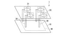
図1は、第1の実施形態による半導体装置1の一例を示す構成図である。
図1に示すように、半導体装置1は、例えば、3次元(3D)NAND型フラッシュメモリ装置であり、メモリ半導体チップ10と、平面バッファチップ20と、TSV(Through-Silicon Via)30とを備えている。[First embodiment]
FIG. 1 is a configuration diagram showing an example of a
As shown in FIG. 1, the
メモリ半導体チップ10は、複数のメモリセル(NAND型フラッシュメモリセル)MCを含むメモリセルアレイ40を備える半導体チップである。なお、メモリセルアレイ40の詳細な構成については後述する。 The
平面バッファチップ20は、メモリ半導体チップ10のビット線(読み出し線)の数に応じた複数のバッファ回路21を備える半導体チップである。バッファ回路21は、メモリセルMCから読み出したデータ及びメモリセルMCに書き込みされるデータを保持する回路である。バッファ回路21は、読み出しの際に、保持したデータを、読み出しデータとして出力する。また、バッファ回路21は、書き込みの際に、保持したデータを、書き込みデータとして、メモリセルMCに出力する。 The
TSV30は、メモリ半導体チップ10及び平面バッファチップ20を厚み方向に貫通して、導体により接続するバンプレスの貫通電極であり、メモリセルMCのビット線と、バッファ回路21とを、メモリ半導体チップ10及び平面バッファチップ20の厚み方向に電気的に接続する。 The TSV 30 is a bumpless through electrode that penetrates the
また、図2は、本実施形態による半導体装置1の一例を示す機能ブロック図である。
図2に示すように、半導体装置1は、アドレスデコーダ11と、電圧生成回路12と、制御回路13と、平面バッファ部200と、メモリセルアレイ40とを備えている。Further, FIG. 2 is a functional block diagram showing an example of the
As shown in FIG. 2, the
アドレスデコーダ11は、入力されたアドレス情報をデコードして、メモリセルアレイ40のメモリセルMCを選択するための制御信号を出力する。
電圧生成回路12は、データ消去の際に必要な消去電圧、及びデータ書き込みの際に必要な書き込み電圧を生成し、生成した消去電圧及び書き込み電圧を、フラッシュメモリであるメモリセルアレイ40に供給する。 The
制御回路13は、外部からの入力に応じて、半導体装置1を制御するロジック回路である。制御回路13は、例えば、メモリセルアレイ40からのデータの読み出し、メモリセルアレイ40のデータ消去、及び書き込みの制御を行う。 The
平面バッファ部200は、所定のデータ長(ビット幅)のデータを一括で読み出し、又は書き込むため、所定のデータ長(ビット幅)分のバッファ回路21を備える。本実施形態では、所定のデータ長(ビット幅)のデータを「ページ」と定義し、平面バッファ部200は、ページデータを保持する。 The
なお、本実施形態におけるバッファ回路21は、TSV30によって厚み方向に引き出されたメモリセルアレイ40のビット線と接続され、平面バッファチップ20の平面状(2次元)に複数配置されている。 Note that the
次に、図3~図6を参照して、本実施形態におけるメモリセルアレイ40の構成について説明する。
図3は、メモリセルアレイ40及び平面バッファチップ20の構成例を示す断面図である。図4は、図3に示すメモリセルアレイ40の一部を拡大した断面図である。図5は、メモリセルアレイ40及び平面バッファチップ20の電気的接続構造を示す構成図である。図6は、図5に示すメモリセルアレイ40及び平面バッファチップ20の電気的接続構造を平面的に見た構成図である。Next, the configuration of the
FIG. 3 is a cross-sectional view showing a configuration example of the
図3~図6に示すように、メモリセルアレイ40は、メモリ半導体チップ10の厚み方向(Z軸方向)に積層された複数のゲートプレート電極(10-SGS、10-0、・・・、10-30、10-31、10-SGD)を備えている。 As shown in FIGS. 3 to 6, the
また、メモリセルアレイ40は、複数のメモリセルMCと、選択トランジスタ(TR1、TR2)とを直列に接続した複数のNANDセルストリングNSを備えている。複数のNANDセルストリングNSは、メモリ半導体チップ10の面内にマトリックス状に配置されている。 Furthermore, the
NANDセルストリングNSは、例えば、ビット線とGND(グランド)線との間に、接地用の選択トランジスタTR1と、32個のメモリセルMCと、データ用の選択トランジスタTR2とが直列に接続されている。 In the NAND cell string NS, for example, a selection transistor TR1 for grounding, 32 memory cells MC, and a selection transistor TR2 for data are connected in series between a bit line and a GND (ground) line. There is.
32個のメモリセルMCは、接地用の選択トランジスタTR1とデータ用の選択トランジスタTR2との間に直列に接続されており、各ゲート端子には、セルゲート信号線(CG0~CG31)が接続され、CG0信号~CG31信号のいずれかの信号により制御される。 The 32 memory cells MC are connected in series between a ground selection transistor TR1 and a data selection transistor TR2, and each gate terminal is connected to a cell gate signal line (CG0 to CG31). It is controlled by any one of the CG0 signal to CG31 signal.
接地用の選択トランジスタTR1は、32個のメモリセルMCと、GND線との間に配置されるNMOSトランジスタ(N型MOSFET(Metal-Oxide-Semiconductor Field-Effect Transistor))であり、ゲート端子にSGS信号線が接続され、SGS信号により制御される。 The selection transistor TR1 for grounding is an NMOS transistor (N-type MOSFET (Metal-Oxide-Semiconductor Field-Effect Transistor)) placed between the 32 memory cells MC and the GND line, and has an SGS transistor at its gate terminal. A signal line is connected and controlled by the SGS signal.
データ用の選択トランジスタTR2は、ビット線と、32個のメモリセルMCとの間に配置されるNMOSトランジスタであり、ゲート端子にいずれかの信号線SGDx0,SGDx1,SGDy0,SGDy1が接続され、SGDx0信号,SGDx1信号,SGDy0信号,SGDy1信号のいずれかの信号により制御される。 The data selection transistor TR2 is an NMOS transistor arranged between the bit line and the 32 memory cells MC, and has its gate terminal connected to one of the signal lines SGDx0, SGDx1, SGDy0, SGDy1, and the SGDx0 signal, SGDx1 signal, SGDy0 signal, and SGDy1 signal.
なお、SGDx0信号,SGDx1信号,SGDy0信号,SGDy1信号、SGS信号、及びCG0信号~CG31信号は、上述したアドレスデコーダ11及び制御回路13によって生成される。 Note that the SGDx0 signal, SGDx1 signal, SGDy0 signal, SGDy1 signal, SGS signal, and CG0 signal to CG31 signal are generated by the
また、接地用の選択トランジスタTR1と、32個のメモリセルMCと、データ用の選択トランジスタTR2とのそれぞれの接続は、貫通電極であるセルピラーCPによって、複数のゲートプレート電極(10-SGS、10-0、・・・、10-30、10-31、10-SGD)を貫通して、厚み方向(Z軸方向)に接続されている。 In addition, the selection transistor TR1 for grounding, the 32 memory cells MC, and the selection transistor TR2 for data are connected to a plurality of gate plate electrodes (10-SGS, 10 -0, . . . , 10-30, 10-31, 10-SGD) and are connected in the thickness direction (Z-axis direction).
次に、図面を参照して、本実施形態による半導体装置1の動作について説明する。
上述した図2において、半導体装置1からデータを読み出す際に、アドレス情報と、例えば、データ読み出しコマンドが半導体装置1に入力されると、まず、アドレスデコーダ11が、入力されたアドレス情報に基づいて、読み出すメモリセルMCを選択するための、SGDx0信号,SGDx1信号,SGDy0信号,SGDy1信号、SGS信号、及びCG0信号~CG31信号を生成する。Next, the operation of the
In FIG. 2 described above, when address information and, for example, a data read command are input to the
具体的には、アドレスデコーダ11は、SGDx0信号,SGDx1信号のいずれかと、SGDy0信号,SGDy1信号のいずれかとをハイ状態(High状態)にし、その他をロウ状態(Low状態)にすることで、NANDセルストリングNSを選択する。また、アドレスデコーダ11は、CG0信号~CG31信号のいずれか1つをロウ状態にし、その他をハイ状態にすることで、選択したNANDセルストリングNSのうちの1つのメモリセルMCを選択する。 Specifically, the
なお、選択されたメモリセルMCは、ゲート端子がロウ状態にされたオフ状態で、電流が流れるか否かによって、“0”又は“1”を読み出すことが可能である。メモリセルMCが保持する“0”又は“1”のデータは、ビット線、及びTSV30を介して、バッファ回路21に入力されて保持される。ここで、メモリセルアレイ40から所定のデータ長(ビット幅)のデータが並列に読み出されて、平面バッファ部200に保持される。 Note that the selected memory cell MC can read "0" or "1" depending on whether or not current flows in an off state in which the gate terminal is set to a low state. The data “0” or “1” held by the memory cell MC is input to the
制御回路13は、データ読み出しコマンドに応じて、平面バッファ部200に読み出しデータを保持させるとともに、保持している読み出しデータを順次外部に出力させる。 The
また、半導体装置1にデータを書き込む際に、アドレス情報と、例えば、データ書き込みコマンドと、書き込みデータとが半導体装置1に入力されると、制御回路13は、書き込みデータを、平面バッファ部200に保持させる。そして、アドレスデコーダ11が、入力されたアドレス情報に基づいて、読み出すメモリセルMCを選択するための、SGDx0信号,SGDx1信号,SGDy0信号,SGDy1信号、SGS信号、及びCG0信号~CG31信号を生成し、制御回路13が、電圧生成回路12から書き込み電圧をメモリセルアレイ40に印加させることにより、所定のデータ長(ビット幅)のデータを並列に書き込む。 Further, when writing data to the
次に、図3~図6を参照して、本実施形態における複数のメモリ半導体チップ10を厚み方向に積層したチップ積層体10A及び平面バッファチップ20の電気的接続構造について説明する。 Next, with reference to FIGS. 3 to 6, an electrical connection structure between the
図3、図4及び図5に示すように、本実施形態の半導体装置1は、上述したメモリ半導体チップ10のメモリセルMCのビット線と、平面バッファチップ20のバッファ回路21とが、メモリ半導体チップ10及び平面バッファチップ20の厚み方向に貫通するTSV30を介して電気的に接続された電気的接続構造を有している。 As shown in FIGS. 3, 4, and 5, in the
また、本実施形態の半導体装置1は、複数のメモリセルMCが半導体基板SBの上に積層された複数のメモリ半導体チップ10を厚み方向に積層したチップ積層体10Aを備えている。 Further, the
半導体基板SBには、例えばデコーダやストリングドライバ等が設けられている。複数のメモリセルMCは、この半導体基板SBの上に積層されて、上述したメモリセルアレイ40を構成している。 For example, a decoder, a string driver, etc. are provided on the semiconductor substrate SB. A plurality of memory cells MC are stacked on this semiconductor substrate SB to constitute the above-mentioned
なお、図3及び図4は、複数のメモリ半導体チップ10及び平面バッファチップ20の各間が離間した状態で図示されているが、実際には、複数のメモリ半導体チップ10及び平面バッファチップ20の各間が直接密着した状態又は中間層(接着剤層等)を挟んで密着した状態となっている。 Although FIGS. 3 and 4 show the plurality of
チップ積層体10Aは、複数のメモリ半導体チップ10の各間にバンプ電極を配置することなく、複数のメモリ半導体チップ10の各間がTSV30を介して電気的に接続されたバンプレス構造を有している。 The
また、各メモリ半導体チップ10は、TSV30を介して複数のメモリセルMCのビット線が厚み方向に電気的に接続された構造を有している。このうち、最下層に位置するメモリ半導体チップ10では、複数のメモリセルMCを厚み方向に貫通した状態でTSV30が設けられている。一方、この最下層よりも上層に位置する残りのメモリ半導体チップ10では、複数のメモリセルMC及び半導体基板SBを厚み方向に貫通した状態でTSV30が設けられている。 Further, each
図3~図6に示すように、チップ積層体10Aは、貫通電極TSV30の周囲に配置された複数のNANDセルストリングNSの各セルピラーCPとTSV30とがビット配線層31及びコンタクトプラグ32を介して電気的に接続された構造を有している。すなわち、これら複数のNANDセルストリングNSは、平面視で貫通電極TSV30の周囲を囲むように配置されると共に、この貫通電極TSV30とビット配線層31及びコンタクトプラグ32を介して並列に接続されている。 As shown in FIGS. 3 to 6, in the chip stacked
ビット配線層31は、各メモリ半導体チップ10の上に積層された層間絶縁層33の層内に設けられて、TSV30と電気的に接続されている。コンタクトプラグ32は、層間絶縁層33を厚み方向に貫いた状態で、ビット配線層31とセルピラーCPとの間を電気的に接続している。なお、ビット配線層31は、コンタクトプラグ32を介することなく、厚み方向に延長されたセルピラーCPと直接接続されていてもよい。 The
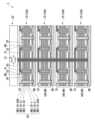
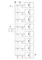
次に、図7~図9を参照して、本実施形態における平面バッファチップ20の構成について説明する。
図7は、本実施形態における平面バッファチップ20が備えるバッファ回路21とセンスアンプ60との接続例を示す構成図である。Next, the configuration of the
FIG. 7 is a configuration diagram showing an example of the connection between the
図7に示すように、平面バッファチップ20が備える複数のバッファ回路21は、各バッファ回路21の一対のビット線毎に設けられた複数のビット配線層22(22_BL0、22_/BL0、22_BL1、22_/BL1、22_BL2、22_/BL2、22_BL3、22_/BL3)を介してセンスアンプ60と電気的に接続されている。センスアンプ60は、バッファ回路21の各々に対応して設けられて、各バッファ回路21から出力されるデータを検出して増幅させる。本例では、4層のビット配線層22を有する。 As shown in FIG. 7, the plurality of
また、図8は、本実施形態における平面バッファチップ20の上に4層のビット配線層22が設けられた半導体装置1の構成例を示す図である。 Further, FIG. 8 is a diagram showing a configuration example of the
図8に示すように、本実施形態におけるバッファ回路21は、TSV30によって厚み方向に引き出されたメモリセルアレイ40のビット線を成すように接続され、平面バッファチップ20の平面状(2次元)に複数配置されている。 As shown in FIG. 8, the
平面バッファチップ20の上には、各バッファ回路21の一対のビット線毎に設けられたビット配線層22が層間絶縁層23を介して積層して配置されている。また、各バッファ回路21の一対のビット線と、各バッファ回路21に対応したビット配線層22とは、それぞれ層間絶縁層23を厚み方向に貫くコンタクトプラグ24を介して電気的に接続されている。なお、図8では、層間絶縁層23を空間として図示している。 Bit wiring layers 22 provided for each pair of bit lines of each
図8では、4つのバッファ回路21(以下、バッファ回路21A,21B,21C,21Dとして区別する。)に対して、4層のビット配線層22(22_BL0、22_/BL0、22_BL1、22_/BL1、22_BL2、22_/BL2、22_BL3、22_/BL3)が、平面バッファチップ20の上に積層して配置された構成を例示している。 In FIG. 8, four bit wiring layers 22 (22_BL0, 22_/BL0, 22_BL1, 22_/BL1, 22_BL2, 22_/BL2, 22_BL3, 22_/BL3) are stacked and arranged on the
すなわち、最下層(1層目)の一対のビット配線層22_BL0、22_/BL0と、バッファ回路21Aの一対のビット線とが、層間絶縁層23を厚み方向に貫く一対のコンタクトプラグ24を介して電気的に接続されている。 That is, the pair of bit wiring layers 22_BL0, 22_/BL0 of the bottom layer (first layer) and the pair of bit lines of the
また、2層目の一対のビット配線層22_BL1、22_/BL1と、バッファ回路21Bの一対のビット線とが、層間絶縁層23を厚み方向に貫く一対のコンタクトプラグ24を介して電気的に接続されている。 Further, the pair of bit wiring layers 22_BL1, 22_/BL1 in the second layer and the pair of bit lines of the
また、3層目の一対のビット配線層22_BL2、22_/BL2と、バッファ回路21Cの一対のビット線とが、層間絶縁層23を厚み方向に貫く一対のコンタクトプラグ24を介して電気的に接続されている。 Further, the pair of bit wiring layers 22_BL2, 22_/BL2 in the third layer and the pair of bit lines of the
また、最上層(4層目)の一対のビット配線層22_BL3、22_/BL3と、バッファ回路21Dの一対のビット線とが、層間絶縁層23を厚み方向に貫く一対のコンタクトプラグ24を介して電気的に接続されている。 Further, the pair of bit wiring layers 22_BL3, 22_/BL3 in the uppermost layer (fourth layer) and the pair of bit lines of the
また、図9は、本実施形態における平面バッファチップ20の上に2層のビット配線層22が設けられた構成例を示す図である。なお、図9では、層間絶縁層23を空間として図示している。 Further, FIG. 9 is a diagram showing a configuration example in which two bit wiring layers 22 are provided on the
図9では、4つのバッファ回路21(21A,21B,21C,21D)に対して、2層のビット配線層22(22_BL00、22_/BL00、22_BL01、22_/BL01、22_BL10、22_/BL10、22_BL11、22_/BL11)が、平面バッファチップ20の上に積層して配置された構成を例示している。 In FIG. 9, two bit wiring layers 22 (22_BL00, 22_/BL00, 22_BL01, 22_/BL01, 22_BL10, 22_/BL10, 22_BL11, 22_/BL11) exemplifies a configuration in which the buffer chips 22_/BL11) are stacked and arranged on the
すなわち、最下層(1層目)の一対のビット配線層22_BL00、22_/BL00と、バッファ回路21Aの一対のビット線とが、層間絶縁層23を厚み方向に貫く一対のコンタクトプラグ24を介して電気的に接続されている。 That is, a pair of bit wiring layers 22_BL00, 22_/BL00 in the bottom layer (first layer) and a pair of bit lines of the
また、一対のビット配線層22_BL00、22_/BL00と同層(1層目)に位置する一対のビット配線層22_BL01、22_/BL01と、バッファ回路21Cの一対のビット線とが、層間絶縁層23を厚み方向に貫く一対のコンタクトプラグ24を介して電気的に接続されている。 Further, a pair of bit wiring layers 22_BL01, 22_/BL01 located in the same layer (first layer) as the pair of bit wiring layers 22_BL00, 22_/BL00 and a pair of bit lines of the
また、最上層(2層目)の一対のビット配線層22_BL10、22_/BL10と、バッファ回路21Bの一対のビット線とが、層間絶縁層23を厚み方向に貫く一対のコンタクトプラグ24を介して電気的に接続されている。 Further, the pair of bit wiring layers 22_BL10, 22_/BL10 in the uppermost layer (second layer) and the pair of bit lines of the
また、一対のビット配線層22_BL10、22_/BL10と同層(2層目)に位置する一対のビット配線層22_BL11、22_/BL11と、バッファ回路21Dの一対のビット線とが、層間絶縁層23を厚み方向に貫く一対のコンタクトプラグ24を介して電気的に接続されている。 Further, a pair of bit wiring layers 22_BL11, 22_/BL11 located in the same layer (second layer) as the pair of bit wiring layers 22_BL10, 22_/BL10 and a pair of bit lines of the
本実施形態の半導体装置1では、これら複数のビット配線層22を介して平面バッファチップ20の複数のバッファ回路21に対してデータを同時にアクセス(読み出し及び書き込み)することが可能である。したがって、本実施形態による半導体装置1では、アクセスを高速化することができる。 In the
また、本実施形態の半導体装置1では、これら複数のビット配線層22を平面バッファチップ20の上に積層して配置することで、各層のビット配線層22のデザインルールを極端に縮小化する必要がない。 Furthermore, in the
なお、本実施形態では、上述した2層や4層のビット配線層22が配置された構成に限らず、ビット配線層22の積層数について適宜変更することが可能であり、例えば、平面バッファチップ20の上に8層のビット配線層22が配置された構成とすることも可能である。また、各層に配置されるビット配線層22の数についても、平面バッファチップ20に配置された複数のバッファ回路21の数に合わせて、適宜変更することが可能である。 Note that this embodiment is not limited to the configuration in which two or four bit wiring layers 22 are arranged as described above, and the number of stacked bit wiring layers 22 can be changed as appropriate. It is also possible to adopt a configuration in which eight bit wiring layers 22 are arranged on top of the
以上説明したように、本実施形態による半導体装置1は、メモリ半導体チップ10と、TSV30(電気的接続構造)とを備える。メモリ半導体チップ10は、複数のメモリセルMCを備える。平面バッファチップ20は、メモリセルMCから読み出したデータ及びメモリセルMCに書き込みされるデータを保持し、保持したデータを出力するバッファ回路21を、複数のメモリセルMCのビット線の数に応じて複数備える半導体チップである。TSV30は、メモリ半導体チップ10のメモリセルMCのビット線と、平面バッファチップ20のバッファ回路21とを、メモリ半導体チップ10及び平面バッファチップ20の厚み方向に、電気的に接続する。また、平面バッファチップ20の上には、各バッファ回路21のビット線と電気的に接続される複数のビット配線層22が積層して配置されている。 As described above, the
これにより、本実施形態による半導体装置1は、バッファ回路21を平面バッファチップ20に、2次元の面状(例えば、XY平面状)に配置することができるため、より多くのメモリセルMCに並列にアクセス(読み出し及び書き込み)を行うことができる。そのよって、本実施形態による半導体装置1は、アクセスを高速化することができる。 As a result, in the
例えば、従来技術では、1次元の線アクセスであったものを、本実施形態による半導体装置1では、2次元という面アクセスにすることで、アクセススピードを、例えば、1桁又は2桁向上させることができる。例えば、従来技術において、1ページの16KB(キロバイト)を1ms(ミリ秒)で書き込むために、16MB/sのスループットである。
これに対して、本実施形態による半導体装置1では、例えば、10ページ分(160KB)を並列処理可能であり、スループットを160MB/sに高速化させることができる。For example, in the
On the other hand, in the
また、本実施形態による半導体装置1は、メモリセルMCのビット線と、平面バッファチップ20のバッファ回路21とを3次元的に厚み方向(Z軸方向)に電気的に接続するため、例えば、従来技術のように、半導体チップの平面上の配線により接続する必要がなく、平面上の配線ピッチにより配線の引き回しが制限されることがない。よって、本実施形態による半導体装置1は、メモリ半導体チップ10のチップサイズを縮小することができる。 Further, in the
また、本実施形態では、メモリ半導体チップ10は、メモリセルMCを含む複数のゲートプレート電極(10-SGS、10-0、・・・、10-30、10-31、10-SGD)が厚み方向に積層されている。TSV30は、積層された複数のゲートプレート電極(10-SGS、10-0、・・・、10-30、10-31、10-SGD)と、平面バッファチップ20とを電気的に接続する。 Further, in the present embodiment, the
これにより、本実施形態による半導体装置1は、メモリ半導体チップ10(メモリセルアレイ40)が、3次元的に構成されており、メモリ半導体チップ10のチップサイズをさらに縮小することができるとともに、アクセスをさらに高速化することができる。 As a result, in the
また、本実施形態では、TSV30は、メモリ半導体チップ10及び平面バッファチップ20を厚み方向に貫通して、導体により接続する貫通電極である。すなわち、TSV30は、バンプレスの貫通電極である。 Further, in this embodiment, the
これにより、本実施形態による半導体装置1は、例えば、従来技術のバンプを用いる場合に比べて、TSV30のビッチを著しく縮小化することが可能であり、平面バッファチップ20にさらに多くのバッファ回路21を配置することが可能である。よって、本実施形態による半導体装置1は、チップサイズをさらに縮小することができるとともに、アクセスをさらに高速化することができる。 As a result, the
また、TSV30は、従来技術のバンプに比べて、半導体チップを薄くすることができるため、接続のインピーダンスを低減することができる。そのため、本実施形態による半導体装置1は、ノイズを低減してアクセスをさらに高速化することができる。 Furthermore, since the
また、本実施形態による半導体装置1は、少なくとも複数のメモリセルMCを厚み方向に貫通するTSV30を介して複数のメモリセルMCのビット線を厚み方向に電気的に接続した電気的接続構造を有している。 Further, the
これにより、メモリ半導体チップ10のNANDセルストリングNS毎に、厚み方向に電気的に接続される複数のメモリセルMCの数が増加した場合でも、これら複数のメモリセルMCの電気的な接続信頼性を確保することが可能である。 As a result, even if the number of multiple memory cells MC electrically connected in the thickness direction increases for each NAND cell string NS of the
さらに、本実施形態による半導体装置1は、複数のメモリセルMCが半導体基板SBの上に積層された複数のメモリ半導体チップ10を厚み方向に積層したチップ積層体10Aにおいて、メモリ半導体チップ10の各間がTSV30を介して電気的に接続された電気的接続構造を有している。 Further, the
これにより、チップ積層体10Aの厚み方向に電気的に接続される複数のメモリセルMCの数を増加させることが可能である。また、メモリ半導体チップ10のNANDセルストリングNS毎に、厚み方向に電気的に接続される複数のメモリセルMCの数に制限(限界)がある場合でも、メモリ半導体チップ10のNANDセルストリングNS毎に、厚み方向に積層される複数のメモリセルMCの電気的な接続信頼性を確保することが可能である。 Thereby, it is possible to increase the number of memory cells MC electrically connected in the thickness direction of the
ところで、例えば3DNANDフラッシュメモリ装置の深孔プロセス工程では、深孔のアスペクト比(孔の直径に対する孔の深さ)に限界があり、一度に貫通できるゲートプレート電極の積層数は64層である。このため、ゲートプレート電極の積層数が128層となる場合、64層のゲートプレート電極の積層工程及び深孔工程を2回繰り返す必要がある。さらに、ゲートプレート電極の積層数が256層となる場合、64層のゲートプレート電極の積層工程及び深孔工程を4回繰り返す必要がある。 By the way, in the deep hole process of a 3D NAND flash memory device, for example, there is a limit to the aspect ratio of the deep hole (the depth of the hole relative to the diameter of the hole), and the number of layers of gate plate electrodes that can be penetrated at one time is 64. Therefore, when the number of stacked gate plate electrodes is 128, it is necessary to repeat the stacking process of 64 layers of gate plate electrodes and the deep hole process twice. Furthermore, when the number of layers of gate plate electrodes is 256, it is necessary to repeat the process of laminating 64 layers of gate plate electrodes and the deep hole process four times.
また、64層のゲートプレート電極の積層工程では、トンネル酸化膜の形成プロセス等で加熱工程が加わるため、熱の影響により微細な周辺回路を構成するトランジスタのソース/ドレインの拡散が進む。その結果、トランジスタ特性が鈍化するだけではなく、ソース/ドレインの距離を離す必要があるため、高性能な微細なトランジスタの作製が困難となる。 Furthermore, in the process of laminating 64 layers of gate plate electrodes, a heating process is added in the process of forming a tunnel oxide film, etc., so the diffusion of the sources/drains of transistors that constitute minute peripheral circuits progresses due to the influence of heat. As a result, not only the transistor characteristics deteriorate, but also the source/drain distance needs to be increased, making it difficult to manufacture a high-performance, fine transistor.
さらに、このような加熱工程が周辺回路のトランジスタに与える影響は、CMOS Next Array(CNA)で周辺回路がメモリアレイの横に配置した場合も、CMOS Under Array(CUA)で直下に配置した場合でも同等に影響を受けることなる。 Furthermore, the effect that such a heating process has on transistors in peripheral circuits is significant regardless of whether the peripheral circuits are placed next to the memory array in a CMOS Next Array (CNA) or directly below the memory array in a CMOS Under Array (CUA). will be equally affected.
一方、厚み方向に電気的に接続される複数のメモリセルの数が増加した場合、メモリセルの直列接続による抵抗の増加に伴って、メモリセルの読出し電流が著しく低下して、ランダムページアクセスのスピードが低下する。その結果、データ読出しの頭出しに時間がかかると言った問題を招く。この場合、アプリケーション側からは、直列接続のメモリセル数が2倍、4倍になることで、消去ブロックのサイズも2倍、4倍になってしまう。 On the other hand, when the number of multiple memory cells that are electrically connected in the thickness direction increases, the read current of the memory cells decreases significantly due to the increase in resistance due to the series connection of memory cells, resulting in random page access. Speed decreases. As a result, a problem arises in that it takes time to locate the beginning of data read. In this case, from the application side, as the number of serially connected memory cells doubles or quadruples, the size of the erase block also doubles or quadruples.
さらに、NANDフラッシュメモリでは、新たなデータを書き換える(上書きする)際に、既に書き込まれている変更しないデータをプロテクトするため、既に消去されたブロックへのデータのコピー(引っ越し作業)が必要である。この場合も、直列接続のメモリセル数が2倍、4倍になることで、データの引っ越し作業が2倍、4倍になってしまう。 Furthermore, in NAND flash memory, when rewriting (overwriting) new data, it is necessary to copy (move) the data to the already erased block in order to protect the data that has already been written and will not be changed. . In this case, as the number of serially connected memory cells doubles or quadruples, the data migration work doubles or quadruples.
これらの問題を回避するためには、厚み方向に積層させるゲートプレート電極に対して、ある周期でビット線とソース線とを挟む方法が考えられる。例えば、64層や128層を1つのNANDメモリセル列(NAND String Unit)として、それぞれのNANDメモリセル列にビット線とソース線を設ける。しかしながら、この場合も、新たな問題点が発生する。それは、結果的にメモリセルアレイの平面レイアウトにおいて、異なるビット線が垂直方向(厚み方向)に積層されるため、そのレイアウトが困難となる。 In order to avoid these problems, a method can be considered in which gate plate electrodes are laminated in the thickness direction, and bit lines and source lines are sandwiched at certain intervals. For example, 64 layers or 128 layers are used as one NAND memory cell string (NAND string unit), and each NAND memory cell string is provided with a bit line and a source line. However, even in this case, new problems arise. As a result, different bit lines are stacked vertically (thickness direction) in the planar layout of the memory cell array, making the layout difficult.
これに対して、本実施形態による半導体装置1では、上述したTSV30による電気的接続構造を採用することで、このような問題を解決することが可能である。すなわち、64層のゲートプレート電極を有するメモリ半導体チップ10を複数作製し、複数のメモリ半導体チップ10を厚み方向に積層したチップ積層体10Aを作製した後に、これら複数のメモリ半導体チップ10を厚み方向に貫通するTSV30を形成する。 In contrast, in the
これにより、1つのメモリ半導体チップにおいて、上述した64層のゲートプレート電極の積層工程及び深孔工程を繰り返す必要がなくなり、加熱工程により周辺回路のトランジスタに与える熱の影響も回避できる。また、チップ積層体10Aを厚み方向に貫通するTSV30によって、複数のメモリセルMCの直列接続による抵抗の増加も抑制できるため、ランダムページアクセスのスピードが低下したり、データの引っ越し作業が遅延したりすることも回避できる。さらに、厚み方向に電気的に接続されるメモリセルMCの数を増加させることが可能である。 This eliminates the need to repeat the above-described 64-layer gate plate electrode stacking process and deep hole process in one memory semiconductor chip, and also avoids the effect of heat on transistors in the peripheral circuit due to the heating process. In addition, the
また、本実施形態による半導体装置1は、TSV30の周囲に配置された複数のNANDセルストリングNSの各セルピラーCPとTSV30とが電気的に接続された電気的接続構造を有している。 Further, the
これにより、TSV30を介して並列接続されるNANDセルストリングNSの数を増加させることで、更なる大容量化を図ることが可能である。 Thereby, by increasing the number of NAND cell strings NS connected in parallel via the
ところで、信号線SGy0,SGy1は、他の信号線SGx0,SGx1やゲートプレート電極10-SGS、10-0、・・・、10-30、10-31、10-SGD)と直交している。信号線SGx0,SGx1やゲートプレート電極10-SGS、10-0、・・・、10-30、10-31、10-SGD)は、SiNのダミー層を除去して、タングステン(W)に置き換えたダマシンプロセスで作製される。一方、信号線SGy0,SGy1は、タングステン(W)を堆積した後に、反応性イオンエッチング(RIE)により加工して作製される。 By the way, the signal lines SGy0, SGy1 are orthogonal to the other signal lines SGx0, SGx1 and the gate plate electrodes 10-SGS, 10-0, . . . , 10-30, 10-31, 10-SGD). For the signal lines SGx0, SGx1 and the gate plate electrodes 10-SGS, 10-0, ..., 10-30, 10-31, 10-SGD), the SiN dummy layer is removed and replaced with tungsten (W). It is manufactured using a damascene process. On the other hand, the signal lines SGy0 and SGy1 are fabricated by depositing tungsten (W) and then processing it by reactive ion etching (RIE).
タングステン(W)を堆積させる厚みは、プロセスで調整可能であるが、例えば、130nmと厚くすることによって、他のダマシンプロセスによる信号線SGx0,SGx1やゲートプレート電極10-SGS、10-0、・・・、10-30、10-31、10-SGD)の厚み20nmに比べて、耐圧を上げている。これは、書き換え時にNANDセルストリングNSに対して高電圧が印加されるため、ビット線とのコンタクト側にパンチスルー現象が発生することを防いでいる。 The thickness of depositing tungsten (W) can be adjusted in the process, but by making it as thick as 130 nm, for example, it can be used to deposit signal lines SGx0, SGx1, gate plate electrodes 10-SGS, 10-0, etc. by other damascene processes. ..., 10-30, 10-31, 10-SGD) with a thickness of 20 nm, the breakdown voltage is increased. This is because a high voltage is applied to the NAND cell string NS during rewriting, thereby preventing punch-through from occurring on the contact side with the bit line.
また、書き込み時には、書込み禁止のNANDセルストリングNSが約10V程度に昇圧される。このため、NANDセルストリングNSからビット線側に電荷がリーク抜けして、書き込みエラーが起こらないように、信号線SGy0,SGy1は、完全にカットオフする。 Furthermore, during writing, the write-inhibited NAND cell string NS is boosted to about 10V. Therefore, the signal lines SGy0 and SGy1 are completely cut off to prevent a write error from occurring due to charge leakage from the NAND cell string NS to the bit line side.
一方、消去時には、NANDセルストリングNSが約20V程度に昇圧される。このとき、信号線SGy0,SGy1は、ビット線側にパンチスルーが発生しないためのバッファトランジスタの役目を果たす。 On the other hand, during erasing, the NAND cell string NS is boosted to about 20V. At this time, the signal lines SGy0 and SGy1 serve as buffer transistors to prevent punch-through from occurring on the bit line side.
また、半導体基板SBには、高耐圧ストリングドライバや行デコーダ等が回路等が作製されている。これらは、メモリセルアレイ40の直下に設けたCUAでも、直下に設けないCANでも、どちらの場合にも、本発明は有効である。 Furthermore, circuits such as a high voltage string driver and a row decoder are fabricated on the semiconductor substrate SB. The present invention is effective in both cases, whether the CUA is provided directly below the
また、半導体基板SBは、単結晶とNANDセルストリングNSの底部をエピタキシャル成長させたp型シリコンを用いて、消去時に半導体基板SBに20Vを印加させるバルク消去を用いてもよい。また、NANDセルストリングNSの直下には、CUAを設け、NANDセルストリングNSは、ポリシリコン基板上に作製してもよい。 Alternatively, the semiconductor substrate SB may be made of single crystal and p-type silicon on which the bottom of the NAND cell string NS is epitaxially grown, and bulk erase may be used in which 20 V is applied to the semiconductor substrate SB during erasing. Further, a CUA may be provided directly below the NAND cell string NS, and the NAND cell string NS may be fabricated on a polysilicon substrate.
この場合、GIDL(Gate Induced Drain Leakage)消去を用いてもよい。GIDL消去は、NANDセルストリングNSを消去時に昇圧する際に、NANDセルストリングNSのソース電圧をNANDセルストリングNSのソース側の選択ゲートの電圧よりも数V高くして、徐々に20V程度まで昇圧させることによって、GIDL電流が発生し、NANDセルストリングNSが消去に必要な20Vに昇圧される。 In this case, GIDL (Gate Induced Drain Leakage) erasure may be used. In GIDL erasing, when boosting the voltage of the NAND cell string NS during erasing, the source voltage of the NAND cell string NS is made several V higher than the voltage of the selection gate on the source side of the NAND cell string NS, and the voltage is gradually increased to about 20 V. As a result, a GIDL current is generated and the NAND cell string NS is boosted to 20V necessary for erasing.
[第2の実施形態]
次に、図面を参照して、第2の実施形態による半導体装置1aについて説明する。[Second embodiment]
Next, a
図10は、第2の実施形態による半導体装置1aの一例を示す構成図である。
図10に示すように、半導体装置1aは、例えば、NAND型フラッシュメモリ装置であり、メモリ半導体チップ10と、デコーダ10Aと、平面バッファチップ20と、TSV30とを備えている。なお、図10において、上述した図1と同一の構成には同一の符号を付与して、その説明を省略する。FIG. 10 is a configuration diagram showing an example of a
As shown in FIG. 10, the
デコーダ10Aは、所定の数のメモリセルのビット線のうちから1つのバッファ回路21を選択するバッファデコーダ部50を備える。なお、本実施形態では、メモリ半導体チップ10と、平面バッファチップ20とは、デデコーダ10Aを経由して、TSV30により接続されている。デコーダ10Aは、メモリ半導体チップ10内に配置されている。 The
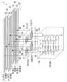
次に、図11~図13を参照して、バッファデコーダ部50の構成について説明する。
図11は、本実施形態におけるバッファデコーダ部50の一例を示す構成図である。
図11に示すように、バッファデコーダ部50は、Xバッファデコーダ51と、Yバッファデコーダ52と、デコーダスイッチ部53とを備えている。Next, the configuration of the
FIG. 11 is a configuration diagram showing an example of the
As shown in FIG. 11, the
Xバッファデコーダ51は、アドレス情報のうちの3ビットをデコードして、X0~X7の選択信号を生成する。 The
Yバッファデコーダ52は、アドレス情報のうちのXバッファデコーダ51とは異なる3ビットをデコードして、Y0~Y7の選択信号を生成する。 The
デコーダスイッチ部53は、Xバッファデコーダ51が生成したX0~X7の選択信号と、Yバッファデコーダ52が生成したY0~Y7の選択信号との組み合わせにより、64本のビット線のうちの1つを選択して、バッファ回路21に接続する。 The
なお、本実施形態では、1つのデコーダスイッチ部53に対して、1つのバッファ回路21が、TSV30により接続される。また、64本のビット線には、それぞれ、1つのNANDセルストリングNSが接続される。 Note that in this embodiment, one
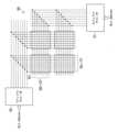
次に、図12及び図13を参照して、デコーダスイッチ部53の構成について説明する。
図12は、本実施形態におけるデコーダスイッチ部53のY0線を選択する場合の構成図である。また、図13は、本実施形態におけるデコーダスイッチ部53のX0線を選択する場合の構成図である。Next, the configuration of the
FIG. 12 is a configuration diagram when selecting the Y0 line of the
図12及び図13に示すように、デコーダスイッチ部53は、選択スイッチ部SW1と、選択スイッチ部SW2とを備える。 As shown in FIGS. 12 and 13, the
選択スイッチ部SW1は、Xバッファデコーダ51が生成したX0~X7の選択信号により制御される選択スイッチである。また、選択スイッチ部SW2は、Yバッファデコーダ52が生成したY0~Y7の選択信号により制御される選択スイッチである。 The selection switch section SW1 is a selection switch controlled by selection signals X0 to X7 generated by the
デコーダスイッチ部53は、選択スイッチ部SW1と、選択スイッチ部SW2とのマトリクスにより、64個のNANDセルストリングNSのうちから1つを選択して、TSV30により、バッファ回路21と接続する。 The
なお、デコーダスイッチ部53と、各NANDセルストリングNSとの間の接続は、NANDセルストリングNS内と同様のポリシリコン等で電気的に接続するものとする。また、選択スイッチ部SW1及び選択スイッチ部SW2は、デコーダ10A上に配置されているものとする。 Note that the
以上説明したように、本実施形態による半導体装置1aは、上述したメモリ半導体チップ10と、平面バッファチップ20と、TSV30(電気的接続構造)とを備え、さらに、バッファデコーダ部50を備える。バッファデコーダ部50は、所定の数(例えば、64本)のメモリセルのビッド線のうちから1つを選択して、バッファ回路21に接続する。 As described above, the
これにより、本実施形態による半導体装置1aは、バッファ回路21のサイズに応じて、適切な本数のビット線のうちから1つを選択して、バッファ回路21に接続することができる。 Thereby, the
なお、本実施形態半導体装置1aでは、図示を省略したものの、上記半導体装置1と同様に、上述したTSV30による電気的接続構造を採用することが可能である。また、上記半導体装置1と同様に、平面バッファチップ20の上に、各バッファ回路21のビット線と電気的に接続される複数のビット配線層22を積層して配置することが可能である。 Note that in the
なお、本発明は、上記の各実施形態に限定されるものではなく、本発明の趣旨を逸脱しない範囲で変更可能である。
例えば、上記半導体装置1については、図14~図16に示すような構成とすることも可能である。Note that the present invention is not limited to the above-described embodiments, and can be modified without departing from the spirit of the present invention.
For example, the
具体的に、図14に示す半導体装置1では、複数のメモリ半導体チップ10を厚み方向に積層したチップ積層体10Aにおいて、TSV30が最下層に位置するメモリ半導体チップ10の複数のメモリセルMCを厚み方向に貫通することなく、この最下層に位置するメモリ半導体チップ10の複数のNANDセルストリングNSとビット配線層31及びコンタクトプラグ32を介して電気的に接続された構成となっている。 Specifically, in the
一方、図15に示す半導体装置1では、複数のメモリ半導体チップ10を厚み方向に積層したチップ積層体10Aの下方に平面バッファチップ20が配置され、これら複数のメモリ半導体チップ10及び平面バッファチップ20が厚み方向に貫通するTSV30を介して電気的に接続された構成となっている。 On the other hand, in the
一方、図16に示す半導体装置1では、図15に示すチップ積層体10Aにより構成されるメモリセルアレイ40と、このメモリセルアレイ40を制御する制御回路13とが、インターポーザIPの上に実装され、このインターポーザIPを介してメモリセルアレイ40と制御回路13とが電気的に接続された構成となっている。 On the other hand, in the
なお、上記の各実施形態において、メモリ半導体チップ10と、平面バッファチップ20との間を、TSV30により接続する例を説明したが、これに限定されるものではなく、バンプなどの他の電気的接続構造によって接続するようにしてもよい。 In each of the above embodiments, an example has been described in which the
また、上記の各実施形態において、半導体装置1(1a)は、フラッシュメモリ装置である例について説明したが、これに限定されるものではなく、他の半導体メモリに適用してもよい。 Further, in each of the above embodiments, an example has been described in which the semiconductor device 1 (1a) is a flash memory device, but the present invention is not limited to this, and may be applied to other semiconductor memories.
また、上記の各実施形態において、平面バッファチップ20を、メモリ半導体チップ10の上側に配置する例を説明したが、これに限定されるものではなく、メモリ半導体チップ10の下側に配置するようにしてもよいし、平面バッファチップ20の上下にメモリ半導体チップ10を配置するようにしてもよい。 Further, in each of the above embodiments, an example has been described in which the
また、上記の第2の実施形態において、バッファデコーダ部50は、平面バッファチップ20とは異なる別のデコーダ10Aに配置する例を説明したが、平面バッファチップ20上に、バッファ回路21とともに配置するようにしてもよい。 Furthermore, in the second embodiment described above, the
また、バッファデコーダ部50を備えずに、例えば、1つのNANDセルストリングNSに対して、1つのバッファ回路21が、TSV30により接続されるようにしてもよい。 Further, without providing the
1、1a 半導体装置
10 メモリ半導体チップ
10A チップ積層体
10-SGS、10-0、10-30、10-31、10-SGD ゲートプレート電極
10A デコーダ
11 アドレスデコーダ
12 電圧生成回路
13 制御回路
20 平面バッファチップ
21 バッファ回路
22 ビット配線層
23 層間絶縁層
24 コンタクトプラグ
30 TSV(貫通電極)
31 ビット配線層
32 コンタクトプラグ
33 層間絶縁層
40 メモリセルアレイ
50 バッファデコーダ部
51 Xバッファデコーダ
52 Yバッファデコーダ
53 デコーダスイッチ部
60 センスアンプ
200 平面バッファ部
CP セルピラー
MC メモリセル
NS NANDセルストリング
SW1、SW2 選択スイッチ部
TR1、TR2 選択トランジスタ1,
31
Claims (5)
Translated fromJapanese前記メモリセルから読み出したデータ及び前記メモリセルに書き込みされるデータを保持し、保持した前記データを出力するバッファ回路を、前記複数のメモリセルのビット線の数に応じて複数備える半導体チップである平面バッファチップと、
前記メモリ半導体チップの前記メモリセルのビット線と、前記平面バッファチップの前記バッファ回路とを、前記メモリ半導体チップ及び平面バッファチップの厚み方向に、電気的に接続する電気的接続構造とを備え、
前記電気的接続構造は、少なくとも前記複数のメモリセルを厚み方向に貫通する貫通電極を介して前記複数のメモリセルのビット線を厚み方向に電気的に接続している
ことを特徴とする半導体装置。A memory semiconductor chip in which a plurality of memory cells are stacked on a semiconductor substrate;
The semiconductor chip includes a plurality of buffer circuits that hold data read from the memory cell and data written to the memory cell, and output the held data in accordance with the number of bit lines of the plurality of memory cells. a planar buffer chip,
an electrical connection structure that electrically connects the bit line of the memory cell of the memory semiconductor chip and the buffer circuit of the planar buffer chip in the thickness direction of the memory semiconductor chip and the planar buffer chip;
The semiconductor device, wherein the electrical connection structure electrically connects the bit lines of the plurality of memory cells in the thickness direction through at least a through electrode that penetrates the plurality of memory cells in the thickness direction. .
前記チップ積層体は、前記メモリ半導体チップの各間が前記貫通電極を介して電気的に接続されている
ことを特徴とする請求項1に記載の半導体装置。comprising a chip stack in which the memory semiconductor chips are stacked in the thickness direction;
2. The semiconductor device according to claim 1, wherein in the chip stack, each of the memory semiconductor chips is electrically connected via the through electrode.
前記貫通電極の周囲に複数配置された前記セルストリングの各セルピラーと前記貫通電極とが電気的に接続されている
ことを特徴とする請求項1又は2に記載の半導体装置。a cell string in which the plurality of memory cells and a selection transistor are electrically connected in the thickness direction via cell pillars;
3. The semiconductor device according to claim 1, wherein each cell pillar of the cell string arranged around the through electrode is electrically connected to the through electrode.
ことを特徴とする請求項1から請求項3のいずれか一項に記載の半導体装置。The electrical connection structure electrically connects the memory semiconductor chip and the planar buffer chip through the through electrode that penetrates the memory semiconductor chip and the planar buffer chip in the thickness direction. The semiconductor device according to any one of claims 1 to 3, characterized in that:
ことを特徴とする請求項1から請求項4のいずれか一項に記載の半導体装置。5. The semiconductor device according to claim 1, wherein the memory cell is a NAND flash memory cell.
Priority Applications (3)
| Application Number | Priority Date | Filing Date | Title |
|---|---|---|---|
| JP2020005051AJP7340178B2 (en) | 2020-01-16 | 2020-01-16 | semiconductor equipment |
| US17/147,658US11437349B2 (en) | 2020-01-16 | 2021-01-13 | Semiconductor device |
| US17/147,633US11404396B2 (en) | 2020-01-16 | 2021-01-13 | Semiconductor device comprising memory semiconductor chip in which memory cell is laminated on semiconductor substrate |
Applications Claiming Priority (1)
| Application Number | Priority Date | Filing Date | Title |
|---|---|---|---|
| JP2020005051AJP7340178B2 (en) | 2020-01-16 | 2020-01-16 | semiconductor equipment |
Publications (2)
| Publication Number | Publication Date |
|---|---|
| JP2021114347A JP2021114347A (en) | 2021-08-05 |
| JP7340178B2true JP7340178B2 (en) | 2023-09-07 |
Family
ID=76857309
Family Applications (1)
| Application Number | Title | Priority Date | Filing Date |
|---|---|---|---|
| JP2020005051AActiveJP7340178B2 (en) | 2020-01-16 | 2020-01-16 | semiconductor equipment |
Country Status (2)
| Country | Link |
|---|---|
| US (2) | US11437349B2 (en) |
| JP (1) | JP7340178B2 (en) |
Citations (1)
| Publication number | Priority date | Publication date | Assignee | Title |
|---|---|---|---|---|
| JP2019528546A (en) | 2016-08-08 | 2019-10-10 | マイクロン テクノロジー,インク. | Multi-deck memory device and operation |
Family Cites Families (12)
| Publication number | Priority date | Publication date | Assignee | Title |
|---|---|---|---|---|
| KR100308479B1 (en) | 1998-08-11 | 2001-11-01 | 윤종용 | Flash memory device used as a boot-up memory in a computer system and a data read method thereof |
| JP5280880B2 (en) | 2009-02-10 | 2013-09-04 | 株式会社日立製作所 | Semiconductor integrated circuit device |
| KR102189757B1 (en) | 2014-07-30 | 2020-12-11 | 삼성전자주식회사 | A semiconductor memory device, a memory system including the same, and a method operating the same |
| KR102449571B1 (en) | 2015-08-07 | 2022-10-04 | 삼성전자주식회사 | Semiconductor Device |
| KR102601214B1 (en) | 2016-05-16 | 2023-11-10 | 삼성전자주식회사 | Memory device having vertical structure and memory system including the same |
| KR20180001296A (en)* | 2016-06-27 | 2018-01-04 | 삼성전자주식회사 | Memory device having vertical structure |
| US10468313B2 (en) | 2017-09-26 | 2019-11-05 | Micron Technology, Inc. | Apparatuses and methods for TSV resistance and short measurement in a stacked device |
| US11211403B2 (en) | 2017-11-27 | 2021-12-28 | Samsung Electronics Co., Ltd. | Nonvolatile memory device having a vertical structure and a memory system including the same |
| KR102408858B1 (en)* | 2017-12-19 | 2022-06-14 | 삼성전자주식회사 | A nonvolatile memory device, a memory system including the same and a method of operating a nonvolatile memory device |
| JP7255797B2 (en) | 2019-03-18 | 2023-04-11 | 本田技研工業株式会社 | semiconductor equipment |
| US11456283B2 (en)* | 2019-12-23 | 2022-09-27 | SK Hynix Inc. | Stacked semiconductor device and test method thereof |
| KR102783893B1 (en) | 2020-01-15 | 2025-03-24 | 삼성전자주식회사 | Three-dimensional semiconductor memory devices |
- 2020
- 2020-01-16JPJP2020005051Apatent/JP7340178B2/enactiveActive
- 2021
- 2021-01-13USUS17/147,658patent/US11437349B2/enactiveActive
- 2021-01-13USUS17/147,633patent/US11404396B2/enactiveActive
Patent Citations (1)
| Publication number | Priority date | Publication date | Assignee | Title |
|---|---|---|---|---|
| JP2019528546A (en) | 2016-08-08 | 2019-10-10 | マイクロン テクノロジー,インク. | Multi-deck memory device and operation |
Also Published As
| Publication number | Publication date |
|---|---|
| US20210225810A1 (en) | 2021-07-22 |
| JP2021114347A (en) | 2021-08-05 |
| US11404396B2 (en) | 2022-08-02 |
| US20210225427A1 (en) | 2021-07-22 |
| US11437349B2 (en) | 2022-09-06 |
Similar Documents
| Publication | Publication Date | Title |
|---|---|---|
| CN108694971A (en) | three-dimensional semiconductor memory device | |
| TW202341439A (en) | Semiconductor storage device | |
| US6067249A (en) | Layout of flash memory and formation method of the same | |
| CN111564449A (en) | Memory element and method of making the same | |
| US11227860B2 (en) | Memory device | |
| US20230005957A1 (en) | Semiconductor memory device | |
| CN113707662A (en) | Vertical memory device | |
| US20240428857A1 (en) | Non-volatile memory device | |
| CN111435663A (en) | Semiconductor device with a plurality of transistors | |
| KR102748985B1 (en) | Nonvolatile memory device including erase transistor | |
| TWI727652B (en) | Memory device | |
| US20240194274A1 (en) | Memory device and operating method thereof | |
| US20240105267A1 (en) | Non-volatile memory device | |
| JP7340178B2 (en) | semiconductor equipment | |
| CN117596880A (en) | Non-volatile memory devices and memory packages | |
| JP7320227B2 (en) | semiconductor equipment | |
| US20250201310A1 (en) | Three-dimensional memory device | |
| TWI858537B (en) | Semiconductor memory devices | |
| US20250142829A1 (en) | Three-dimensional memory device | |
| US20250081472A1 (en) | Non-volatile memory device | |
| EP4336985A1 (en) | Semiconductor memory device and electronic system including the same | |
| US20250014645A1 (en) | Nonvolatile memory devices and memory packages including the same | |
| KR20250032052A (en) | Semiconductor memory device and manufacturing method of semiconductor memory device | |
| JP2024155149A (en) | Semiconductor memory device | |
| KR20250030223A (en) | Memory device and manufacturing method of the memory device |
Legal Events
| Date | Code | Title | Description |
|---|---|---|---|
| RD01 | Notification of change of attorney | Free format text:JAPANESE INTERMEDIATE CODE: A7426 Effective date:20200220 | |
| A521 | Request for written amendment filed | Free format text:JAPANESE INTERMEDIATE CODE: A821 Effective date:20200220 | |
| A521 | Request for written amendment filed | Free format text:JAPANESE INTERMEDIATE CODE: A523 Effective date:20200421 | |
| A521 | Request for written amendment filed | Free format text:JAPANESE INTERMEDIATE CODE: A523 Effective date:20200421 | |
| A621 | Written request for application examination | Free format text:JAPANESE INTERMEDIATE CODE: A621 Effective date:20221012 | |
| TRDD | Decision of grant or rejection written | ||
| A977 | Report on retrieval | Free format text:JAPANESE INTERMEDIATE CODE: A971007 Effective date:20230726 | |
| A01 | Written decision to grant a patent or to grant a registration (utility model) | Free format text:JAPANESE INTERMEDIATE CODE: A01 Effective date:20230801 | |
| A61 | First payment of annual fees (during grant procedure) | Free format text:JAPANESE INTERMEDIATE CODE: A61 Effective date:20230816 | |
| R150 | Certificate of patent or registration of utility model | Ref document number:7340178 Country of ref document:JP Free format text:JAPANESE INTERMEDIATE CODE: R150 | |
| S533 | Written request for registration of change of name | Free format text:JAPANESE INTERMEDIATE CODE: R313533 | |
| R350 | Written notification of registration of transfer | Free format text:JAPANESE INTERMEDIATE CODE: R350 |