JP7338975B2 - semiconductor memory device - Google Patents
semiconductor memory deviceDownload PDFInfo
- Publication number
- JP7338975B2 JP7338975B2JP2019004399AJP2019004399AJP7338975B2JP 7338975 B2JP7338975 B2JP 7338975B2JP 2019004399 AJP2019004399 AJP 2019004399AJP 2019004399 AJP2019004399 AJP 2019004399AJP 7338975 B2JP7338975 B2JP 7338975B2
- Authority
- JP
- Japan
- Prior art keywords
- contact
- wiring
- region
- electrically connected
- semiconductor
- Prior art date
- Legal status (The legal status is an assumption and is not a legal conclusion. Google has not performed a legal analysis and makes no representation as to the accuracy of the status listed.)
- Active
Links
Images


Classifications
- H—ELECTRICITY
- H10—SEMICONDUCTOR DEVICES; ELECTRIC SOLID-STATE DEVICES NOT OTHERWISE PROVIDED FOR
- H10B—ELECTRONIC MEMORY DEVICES
- H10B12/00—Dynamic random access memory [DRAM] devices
- H10B12/30—DRAM devices comprising one-transistor - one-capacitor [1T-1C] memory cells
- H—ELECTRICITY
- H10—SEMICONDUCTOR DEVICES; ELECTRIC SOLID-STATE DEVICES NOT OTHERWISE PROVIDED FOR
- H10B—ELECTRONIC MEMORY DEVICES
- H10B41/00—Electrically erasable-and-programmable ROM [EEPROM] devices comprising floating gates
- H10B41/20—Electrically erasable-and-programmable ROM [EEPROM] devices comprising floating gates characterised by three-dimensional arrangements, e.g. with cells on different height levels
- H—ELECTRICITY
- H01—ELECTRIC ELEMENTS
- H01L—SEMICONDUCTOR DEVICES NOT COVERED BY CLASS H10
- H01L23/00—Details of semiconductor or other solid state devices
- H01L23/52—Arrangements for conducting electric current within the device in operation from one component to another, i.e. interconnections, e.g. wires, lead frames
- H01L23/522—Arrangements for conducting electric current within the device in operation from one component to another, i.e. interconnections, e.g. wires, lead frames including external interconnections consisting of a multilayer structure of conductive and insulating layers inseparably formed on the semiconductor body
- H01L23/528—Layout of the interconnection structure
- H—ELECTRICITY
- H10—SEMICONDUCTOR DEVICES; ELECTRIC SOLID-STATE DEVICES NOT OTHERWISE PROVIDED FOR
- H10B—ELECTRONIC MEMORY DEVICES
- H10B12/00—Dynamic random access memory [DRAM] devices
- H10B12/50—Peripheral circuit region structures
- H—ELECTRICITY
- H10—SEMICONDUCTOR DEVICES; ELECTRIC SOLID-STATE DEVICES NOT OTHERWISE PROVIDED FOR
- H10B—ELECTRONIC MEMORY DEVICES
- H10B43/00—EEPROM devices comprising charge-trapping gate insulators
- H10B43/20—EEPROM devices comprising charge-trapping gate insulators characterised by three-dimensional arrangements, e.g. with cells on different height levels
- H—ELECTRICITY
- H10—SEMICONDUCTOR DEVICES; ELECTRIC SOLID-STATE DEVICES NOT OTHERWISE PROVIDED FOR
- H10D—INORGANIC ELECTRIC SEMICONDUCTOR DEVICES
- H10D62/00—Semiconductor bodies, or regions thereof, of devices having potential barriers
- H10D62/10—Shapes, relative sizes or dispositions of the regions of the semiconductor bodies; Shapes of the semiconductor bodies
- H10D62/13—Semiconductor regions connected to electrodes carrying current to be rectified, amplified or switched, e.g. source or drain regions
- H10D62/149—Source or drain regions of field-effect devices
- H10D62/151—Source or drain regions of field-effect devices of IGFETs
- H—ELECTRICITY
- H10—SEMICONDUCTOR DEVICES; ELECTRIC SOLID-STATE DEVICES NOT OTHERWISE PROVIDED FOR
- H10D—INORGANIC ELECTRIC SEMICONDUCTOR DEVICES
- H10D62/00—Semiconductor bodies, or regions thereof, of devices having potential barriers
- H10D62/10—Shapes, relative sizes or dispositions of the regions of the semiconductor bodies; Shapes of the semiconductor bodies
- H10D62/17—Semiconductor regions connected to electrodes not carrying current to be rectified, amplified or switched, e.g. channel regions
- H10D62/213—Channel regions of field-effect devices
- H10D62/221—Channel regions of field-effect devices of FETs
- H10D62/235—Channel regions of field-effect devices of FETs of IGFETs
- H10D62/292—Non-planar channels of IGFETs
- H—ELECTRICITY
- H10—SEMICONDUCTOR DEVICES; ELECTRIC SOLID-STATE DEVICES NOT OTHERWISE PROVIDED FOR
- H10D—INORGANIC ELECTRIC SEMICONDUCTOR DEVICES
- H10D62/00—Semiconductor bodies, or regions thereof, of devices having potential barriers
- H10D62/80—Semiconductor bodies, or regions thereof, of devices having potential barriers characterised by the materials
- H10D62/82—Heterojunctions
- H10D62/822—Heterojunctions comprising only Group IV materials heterojunctions, e.g. Si/Ge heterojunctions
- H—ELECTRICITY
- H01—ELECTRIC ELEMENTS
- H01L—SEMICONDUCTOR DEVICES NOT COVERED BY CLASS H10
- H01L23/00—Details of semiconductor or other solid state devices
- H01L23/52—Arrangements for conducting electric current within the device in operation from one component to another, i.e. interconnections, e.g. wires, lead frames
- H01L23/522—Arrangements for conducting electric current within the device in operation from one component to another, i.e. interconnections, e.g. wires, lead frames including external interconnections consisting of a multilayer structure of conductive and insulating layers inseparably formed on the semiconductor body
- H01L23/5226—Via connections in a multilevel interconnection structure
- H—ELECTRICITY
- H10—SEMICONDUCTOR DEVICES; ELECTRIC SOLID-STATE DEVICES NOT OTHERWISE PROVIDED FOR
- H10D—INORGANIC ELECTRIC SEMICONDUCTOR DEVICES
- H10D1/00—Resistors, capacitors or inductors
- H10D1/60—Capacitors
- H10D1/68—Capacitors having no potential barriers
- H10D1/692—Electrodes
Landscapes
- Physics & Mathematics (AREA)
- Geometry (AREA)
- Condensed Matter Physics & Semiconductors (AREA)
- General Physics & Mathematics (AREA)
- Engineering & Computer Science (AREA)
- Computer Hardware Design (AREA)
- Microelectronics & Electronic Packaging (AREA)
- Power Engineering (AREA)
- Semiconductor Memories (AREA)
- Thin Film Transistor (AREA)
- Internal Circuitry In Semiconductor Integrated Circuit Devices (AREA)
- Non-Volatile Memory (AREA)
Description
Translated fromJapanese本発明は半導体素子に係り、さらに詳細には集積度が向上された3次元半導体メモリ素子に係る。 The present invention relates to a semiconductor device, and more particularly, to a three-dimensional semiconductor memory device with improved integration.
消費者が要求する優れた性能及び低廉な価額を充足させるために半導体素子の集積度を増加させることが要求されている。半導体素子の場合、その集積度は製品の価額を決定する重要な要因であるので、特に増加された集積度が要求されている。従来の2次元又は平面的な半導体素子の場合、その集積度は単位メモリセルが占有する面積によって主に決定されるので、微細パターン形成技術の水準に大きく影響を受ける。しかし、パターンの微細化のためには超高価の装備を必要とするので、2次元半導体素子の集積度は増加しているが、相変わらず制限的である。したがって、3次元的に配列されるメモリセルを具備する3次元半導体メモリ素子が提案されている。 There is a demand for increasing the degree of integration of semiconductor devices to meet consumer demand for superior performance and low cost. In the case of semiconductor devices, since the degree of integration is an important factor in determining the price of products, there is a demand for an increased degree of integration. In the case of conventional two-dimensional or planar semiconductor devices, the degree of integration is determined mainly by the area occupied by a unit memory cell, and is greatly affected by the level of micropatterning technology. However, miniaturization of patterns requires extremely expensive equipment, and thus the degree of integration of two-dimensional semiconductor devices is increasing, but is still limited. Therefore, a three-dimensional semiconductor memory device having memory cells arranged three-dimensionally has been proposed.
本発明が解決しようとする課題は集積度が向上された3次元半導体メモリ素子を提供することにある。 SUMMARY OF THE INVENTION An object of the present invention is to provide a three-dimensional semiconductor memory device with improved integration.
本発明の概念に係る、半導体メモリ素子は、基板の上の第1積層構造体及び第2積層構造体と、前記第1及び第2積層構造体上の第1配線及び第2配線と、を含むことができる。前記第1及び第2積層構造体の各々は、垂直方向に積層された半導体パターンと、前記半導体パターンと連結され、水平方向に延在される導電ラインと、前記半導体パターンと隣接して垂直方向に延在されるゲート電極と、を含むことができる。前記第1積層構造体の前記導電ラインは第1導電ラインを含み、前記第2積層構造体の前記導電ラインは前記第1導電ラインと同一レベルに位置する第2導電ラインを含み、前記第1配線は前記第1及び第2導電ラインのうちの少なくとも1つと電気的に連結され、前記第2配線は前記第1及び第2積層構造体の前記ゲート電極のうちの少なくとも1つと電気的に連結されることができる。 A semiconductor memory device according to the concept of the present invention includes a first stacked structure and a second stacked structure on a substrate, and first wiring and second wiring on the first and second stacked structures. can contain. Each of the first and second stack structures includes a vertically stacked semiconductor pattern, a conductive line connected to the semiconductor pattern and extending in a horizontal direction, and a vertically adjacent semiconductor pattern. and a gate electrode extending to the . The conductive lines of the first stack structure include first conductive lines, the conductive lines of the second stack structure include second conductive lines located at the same level as the first conductive lines, and the first A wiring is electrically connected to at least one of the first and second conductive lines, and the second wiring is electrically connected to at least one of the gate electrodes of the first and second stack structures. can be
本発明の他の概念に係る、半導体メモリ素子は、セル領域及びコンタクト領域を含む基板と、各々が第1不純物領域、第2不純物領域、及び前記第1及び第2不純物領域の間のチャネル領域と、を含む、前記セル領域上で垂直方向に積層された半導体パターンと、前記セル領域から前記コンタクト領域に水平方向に延長され、前記半導体パターンの前記第1不純物領域と連結される第1導電ラインと、前記半導体パターンの前記第2不純物領域と連結されるキャパシターと、前記コンタクト領域上の前記第1導電ラインと接触するコンタクトと、を含むことができる。前記コンタクトは、第1コンタクト及び前記第1コンタクトより前記セル領域にさらに近い第2コンタクトを含み、前記第2コンタクトの底面のレベルは前記第1コンタクトの底面のレベルよりさらに高い。 According to another aspect of the present invention, a semiconductor memory device includes: a substrate including a cell region and a contact region; and a first impurity region, a second impurity region, and a channel region between the first and second impurity regions, respectively. a semiconductor pattern vertically stacked on the cell region; and a first conductor horizontally extending from the cell region to the contact region and connected to the first impurity region of the semiconductor pattern. A line, a capacitor connected to the second impurity region of the semiconductor pattern, and a contact contacting the first conductive line on the contact region may be included. The contacts include a first contact and a second contact that is closer to the cell region than the first contact, and the bottom level of the second contact is higher than the bottom level of the first contact.
本発明のその他の概念に係る、半導体メモリ素子は、基板の上の第1積層構造体及び第2積層構造体と、前記第1及び第2積層構造体上の第1配線及び第2配線と、を含むことができる。前記第1配線は第1方向に延在され、前記第2配線は前記第1方向と交差する第2方向に延在され、前記第1及び第2積層構造体の各々は、3次元的に配列されたメモリセルトランジスタと、水平方向に配列された前記メモリセルトランジスタと連結されるビットラインと、垂直方向に配列された前記メモリセルトランジスタと連結されるワードラインと、を含むことができる。前記基板のコンタクト領域上で、前記第1配線は前記第1及び第2積層構造体の前記ビットラインのうちの少なくとも1つと電気的に連結され、前記基板のセル領域上で、前記第2配線は前記第1及び第2積層構造体の前記ワードラインのうちの少なくとも1つと電気的に連結されることができる。 According to another concept of the present invention, a semiconductor memory device includes a first laminated structure and a second laminated structure on a substrate, and first wirings and second wirings on the first and second laminated structures. , can be included. The first wiring extends in a first direction, the second wiring extends in a second direction crossing the first direction, and each of the first and second stacked structures is three-dimensionally The memory cell transistors may be arranged, bit lines connected to the horizontally arranged memory cell transistors, and word lines connected to the vertically arranged memory cell transistors. The first wiring is electrically connected to at least one of the bit lines of the first and second stack structures on the contact region of the substrate, and the second wiring on the cell region of the substrate. may be electrically connected to at least one of the word lines of the first and second stack structures.
本発明の実施形態に係る3次元半導体メモリ素子は、メモリセルが3次元的に基板上に配列されることができる。ビットライン及びワードラインがメモリセル上の配線を通じて周辺回路領域と効率的に連結されることができる。 In a three-dimensional semiconductor memory device according to an embodiment of the present invention, memory cells may be three-dimensionally arranged on a substrate. Bitlines and wordlines can be efficiently connected to the peripheral circuit area through interconnections on the memory cells.
図1は本発明の実施形態に係る3次元半導体メモリ素子のセルアレイを示す簡略回路図である。図1を参照すれば、本発明の実施形態に係る3次元半導体メモリ素子のセルアレイは複数のサブセルアレイSCAを含む。サブセルアレイSCAは第2方向D2に沿って配列される。 FIG. 1 is a simplified circuit diagram showing a cell array of a 3D semiconductor memory device according to an embodiment of the present invention. Referring to FIG. 1, a cell array of a 3D semiconductor memory device according to an embodiment of the present invention includes a plurality of sub-cell arrays SCA. The sub-cell array SCA is arranged along the second direction D2.
各々のサブセルアレイSCAは複数のビットラインBL、複数のワードラインWL、及び複数のメモリセルトランジスタMCTを含む。1つのワードラインWLと1つのビットラインBLとの間に1つのメモリセルトランジスタMCTが配置される。 Each sub-cell array SCA includes a plurality of bitlines BL, a plurality of wordlines WL, and a plurality of memory cell transistors MCT. One memory cell transistor MCT is arranged between one word line WL and one bit line BL.
ビットラインBLは基板から離隔されて、前記基板上に配置される導電性パターン(例えば、金属ライン)である。ビットラインBLは第1方向D1に延在される。1つのサブセルアレイSCA内のビットラインBLは垂直方向(即ち、第3方向D3)に互いに離隔される。 A bit line BL is a conductive pattern (eg, a metal line) disposed on the substrate, spaced apart from the substrate. The bitline BL extends in the first direction D1. The bitlines BL in one sub-cell array SCA are separated from each other in the vertical direction (ie, the third direction D3).
ワードラインWLは基板から垂直方向(即ち、第3方向D3)に延在される導電性パターン(例えば、金属ライン)である。1つのサブセルアレイSCA内のワードラインWLは第1方向D1に互いに離隔される。 The word lines WL are conductive patterns (eg, metal lines) extending vertically (ie, the third direction D3) from the substrate. Word lines WL in one sub-cell array SCA are spaced apart from each other in the first direction D1.
メモリセルトランジスタMCTのゲートはワードラインWLに連結され、メモリセルトランジスタMCTのソースはビットラインBLに連結される。各々のメモリセルトランジスタMCTは情報格納要素DSを含む。例えば、情報格納要素DSはキャパシターであり、メモリセルトランジスタMCTのドレインは前記キャパシターの第1電極に連結される。前記キャパシターの第2電極は接地配線PPと連結される。 A gate of the memory cell transistor MCT is connected to the wordline WL, and a source of the memory cell transistor MCT is connected to the bitline BL. Each memory cell transistor MCT includes an information storage element DS. For example, the information storage element DS is a capacitor, and the drain of the memory cell transistor MCT is connected to the first electrode of the capacitor. A second electrode of the capacitor is connected to a ground line PP.
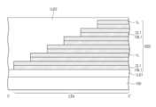
図2は本発明の実施形態に係る3次元半導体メモリ素子を示す斜視図である。図3A、図3B、及び図3Cは各々図2のA-A’線、B-B’線、及びC-C’線に沿う断面図である。図3Dは図3AのM領域を拡大した断面図である。 FIG. 2 is a perspective view showing a 3D semiconductor memory device according to an embodiment of the present invention. 3A, 3B, and 3C are cross-sectional views along lines A-A', B-B', and C-C' of FIG. 2, respectively. FIG. 3D is a cross-sectional view enlarging the M region of FIG. 3A.
図1、図2、及び図3A乃至図3Dを参照すれば、セル領域CAR及びコンタクト領域CTRを含む基板100が提供される。基板100上に第1層間絶縁膜ILD1が提供される。基板100はシリコン基板、ゲルマニウム基板、又はシリコン-ゲルマニウム基板である。 1, 2, and 3A-3D, a
基板100上に第1乃至第4積層構造体SS1-SS4が提供される。第1乃至第4積層構造体SS1-SS4は第1層間絶縁膜ILD1を介して基板100と垂直方向に離隔される。第1乃至第4積層構造体SS1-SS4は互いに平行に第1方向D1に延在される。第1乃至第4積層構造体SS1-SS4は第2方向D2に沿って配列される。第1乃至第4積層構造体SS1-SS4の各々は、先に図1を参照して説明したサブセルアレイSCAを含む。 First to fourth stack structures SS1-SS4 are provided on the
各々の第1乃至第4積層構造体SS1-SS4は、第1層間絶縁膜ILD1上に互いに交互に積層された半導体パターンSP及び絶縁膜ILを含む。垂直方向に積層された半導体パターンSPは絶縁膜ILによって互いに垂直方向に離隔される。互いに垂直方向に隣接する一対の半導体パターンSPの間に絶縁膜ILが介在される。絶縁膜ILはシリコン酸化膜、シリコン窒化膜、シリコン酸窒化膜、炭素含有シリコン酸化膜、炭素含有シリコン窒化膜、及び炭素含有シリコン酸窒化膜からなる群から選択されることができる。 Each of the first to fourth stacked structures SS1-SS4 includes semiconductor patterns SP and insulating layers IL alternately stacked on the first interlayer insulating layer ILD1. The vertically stacked semiconductor patterns SP are vertically separated from each other by an insulating layer IL. An insulating film IL is interposed between a pair of vertically adjacent semiconductor patterns SP. The insulating film IL can be selected from the group consisting of a silicon oxide film, a silicon nitride film, a silicon oxynitride film, a carbon-containing silicon oxide film, a carbon-containing silicon nitride film, and a carbon-containing silicon oxynitride film.
各々の半導体パターンSPは第2方向D2に延在されるライン形状、バー(bar)形状、又は柱形状を有する。一例として、半導体パターンSPはシリコン、ゲルマニウム、シリコン-ゲルマニウム又はIGZO(Indium Gallium Zinc Oxide)を含む。各々の半導体パターンSPは第1不純物領域SD1、第2不純物領域SD2、及びチャネル領域CHを含む。 Each semiconductor pattern SP has a line shape, a bar shape, or a column shape extending in the second direction D2. For example, the semiconductor pattern SP includes silicon, germanium, silicon-germanium, or IGZO (Indium Gallium Zinc Oxide). Each semiconductor pattern SP includes a first impurity region SD1, a second impurity region SD2, and a channel region CH.
チャネル領域CHは第1及び第2不純物領域SD1、SD2の間に配置される。第1及び第2不純物領域SD1、SD2は第1導電型(例えば、n型)を有する。チャネル領域CHはドーピングされないか、或いは第1導電型とは異なる第2導電型(例えば、p型)を有する。 A channel region CH is disposed between the first and second impurity regions SD1 and SD2. The first and second impurity regions SD1 and SD2 have a first conductivity type (eg, n-type). The channel region CH is undoped or has a second conductivity type (eg p-type) different from the first conductivity type.
チャネル領域CHは、図1のメモリセルトランジスタMCTのチャネルに該当する。第1及び第2不純物領域SD1、SD2は、図1のメモリセルトランジスタMCTのソース及びドレインに各々該当する。 Channel region CH corresponds to the channel of memory cell transistor MCT in FIG. The first and second impurity regions SD1 and SD2 correspond to the source and drain of the memory cell transistor MCT of FIG. 1, respectively.
半導体パターンSPは基板100のセル領域CAR上に提供される。第1乃至第4積層構造体SS1-SS4の各々は、第1乃至第4列R1-R4の半導体パターンSPを含む。第1乃至第4列R1-R4の各々は、垂直方向に積層されて互いに重畳される半導体パターンSPを含む。一例として、第1乃至第4列R1-R4の各々の半導体パターンSPの数は6つに例示されるが、これに特別に制限されることではない。第1乃至第4列R1-R4は第1方向D1に沿って互いに離隔されて配列される。 A semiconductor pattern SP is provided on the cell area CAR of the
各々の第1乃至第4積層構造体SS1-SS4は、垂直方向に積層された第1導電ラインCL1をさらに含む。垂直方向に積層された第1導電ラインCL1は絶縁膜ILによって互いに垂直方向に離隔される。互いに垂直方向に隣接する一対の第1導電ラインCL1の間に絶縁膜ILが介在される。 Each of the first to fourth stack structures SS1-SS4 further includes a vertically stacked first conductive line CL1. The vertically stacked first conductive lines CL1 are vertically separated from each other by an insulating layer IL. An insulating layer IL is interposed between a pair of first conductive lines CL1 vertically adjacent to each other.
第1導電ラインCL1は第1方向D1に延在されるライン形状又はバー形状を有する。第1導電ラインCL1は基板100のセル領域CARからコンタクト領域CTRまで延長される。 The first conductive line CL1 has a line shape or a bar shape extending in the first direction D1. The first conductive line CL1 extends from the cell area CAR of the
各々の第1導電ラインCL1は半導体パターンSPと直接接触する。一例として、各々の第1導電ラインCL1は半導体パターンSPと実質的に同一なレベルに位置する。各々の第1導電ラインCL1は半導体パターンSPの第1不純物領域SD1と連結される。各々の第1導電ラインCL1から、それと同一なレベルに位置する第1乃至第4列R1-R4の半導体パターンSPが第2方向D2に延在される。 Each first conductive line CL1 is in direct contact with the semiconductor pattern SP. For example, each first conductive line CL1 is positioned at substantially the same level as the semiconductor pattern SP. Each first conductive line CL1 is connected to the first impurity region SD1 of the semiconductor pattern SP. From each first conductive line CL1, the semiconductor patterns SP of the first to fourth columns R1-R4 located at the same level as the first conductive line CL1 extend in the second direction D2.
図3Cを参照すれば、基板100のコンタクト領域CTR上の第1乃至第4積層構造体SS1-SS4の各々は階段式構造を有する。コンタクト領域CTR上に積層された第1導電ラインCL1の第1方向D1への長さは、基板100の上面から遠くなるほど、減少される。例えば、積層された第1導電ラインCL1の中で最下部の第1導電ラインCL1の長さが残りの第1導電ラインCL1の各々の長さよりさらに長い。積層された第1導電ラインCL1の中で最上部の第1導電ラインCL1の長さが残りの第1導電ラインCL1の各々の長さよりさらに短い。 Referring to FIG. 3C, each of the first to fourth stack structures SS1-SS4 on the contact region CTR of the
第1導電ラインCL1は導電物質を含む。一例として、前記導電物質はドーピングされた半導体物質(ドーピングされたシリコン、ドーピングされたゲルマニウム等)、導電性金属窒化膜(窒化チタニウム、窒化タンタル等)、金属(タングステン、チタニウム、タンタル等)、及び金属-半導体化合物(タングステンシリサイド、コバルトシリサイド、チタニウムシリサイド等)の中でいずれか1つである。第1導電ラインCL1は図1を参照して説明したビットラインBLである。 The first conductive line CL1 includes a conductive material. By way of example, the conductive material may be a doped semiconductor material (doped silicon, doped germanium, etc.), a conductive metal nitride (titanium nitride, tantalum nitride, etc.), a metal (tungsten, titanium, tantalum, etc.), and Any one of metal-semiconductor compounds (tungsten silicide, cobalt silicide, titanium silicide, etc.). The first conductive line CL1 is the bit line BL described with reference to FIG.
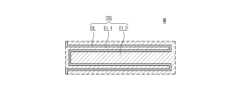
各々の第1乃至第4積層構造体SS1-SS4は、垂直方向に積層された情報格納要素DSをさらに含む。垂直方向に積層された情報格納要素DSは絶縁膜ILによって互いに垂直方向に離隔される。各々の情報格納要素DSは、各々の半導体パターンSPから第2方向D2に延在される。 Each of the first to fourth stacked structures SS1-SS4 further includes vertically stacked information storage elements DS. The vertically stacked information storage elements DS are vertically separated from each other by an insulating layer IL. Each information storage element DS extends in the second direction D2 from each semiconductor pattern SP.
各々の情報格納要素DSは各々の半導体パターンSPと直接接触する。一例として、各々の情報格納要素DSは各々の半導体パターンSPと実質的に同一なレベルに位置する。各々の情報格納要素DSは半導体パターンSPの各々の第2不純物領域SD2と連結される。 Each information storage element DS directly contacts each semiconductor pattern SP. For example, each information storage element DS is positioned at substantially the same level as each semiconductor pattern SP. Each information storage element DS is connected to each second impurity region SD2 of the semiconductor pattern SP.
図3Dを参照すれば、各々の情報格納要素DSは第1電極EL1、誘電膜DL、及び第2電極EL2を含む。再び言えば、本発明の実施形態に係る情報格納要素DSはキャパシターである。 Referring to FIG. 3D, each information storage element DS includes a first electrode EL1, a dielectric layer DL, and a second electrode EL2. Again, the information storage element DS according to embodiments of the invention is a capacitor.
第1電極EL1は半導体パターンSPの第2不純物領域SD2に直接連結される。第1電極EL1は中が空いたシリンダー(cylinder)形状を有する。第1電極EL1は金属物質、金属窒化膜、及び金属シリサイドの中で少なくとも1つを含む。例えば、第1電極EL1はコバルト、チタニウム、ニッケル、タングステン、及びモリブデンのような高融点金属膜を含む。第1電極EL1はチタニウム窒化膜、チタニウムシリコン窒化膜、チタニウムアルミニウム窒化膜、タンタル窒化膜、タンタルシリコン窒化膜、タンタルアルミニウム窒化膜、及びタングステン窒化膜のような金属窒化膜を含む。 The first electrode EL1 is directly connected to the second impurity region SD2 of the semiconductor pattern SP. The first electrode EL1 has a hollow cylinder shape. The first electrode EL1 includes at least one of a metal material, a metal nitride layer, and a metal silicide. For example, the first electrode EL1 includes a refractory metal film such as cobalt, titanium, nickel, tungsten, and molybdenum. The first electrode EL1 includes a metal nitride layer such as a titanium nitride layer, a titanium silicon nitride layer, a titanium aluminum nitride layer, a tantalum nitride layer, a tantalum silicon nitride layer, a tantalum aluminum nitride layer, and a tungsten nitride layer.
誘電膜DLは第1電極EL1と第2電極EL2との間に介在される。誘電膜DLは第1電極EL1の内側壁を直接覆う。例えば、誘電膜DLはハフニウム酸化物、ジルコニウム酸化物、アルミニウム酸化物、ランタン酸化物、タンタル酸化物、及びチタニウム酸化物のような金属酸化物及びSrTiO3(STO)、(Ba、Sr)TiO3(BST)、BaTiO3、PZT、PLZTのようなペロブスカイト(perovskite)構造の誘電物質の中で少なくとも1つを含む。 The dielectric layer DL is interposed between the first electrode EL1 and the second electrode EL2. The dielectric layer DL directly covers the inner sidewalls of the first electrode EL1. For example, the dielectric film DL can be made of metal oxides such as hafnium oxide, zirconium oxide, aluminum oxide, lanthanum oxide, tantalum oxide, and titanium oxide, and SrTiO3 (STO), (Ba, Sr)TiO3 (BST). ), BaTiO3, PZT, and PLZT.
第2電極EL2は誘電膜DL上に提供される。第2電極EL2はシリンダー形状の第1電極EL1の内部を満たす。第2電極EL2は後述する第3導電ラインCL3と連結される。第2電極EL2は不純物がドーピングされたシリコン、金属物質、金属窒化膜、及び金属シリサイドの中の少なくとも1つを含む。一例として、第2電極EL2は第1電極EL1と実質的に同一な物質を含む。 A second electrode EL2 is provided on the dielectric layer DL. The second electrode EL2 fills the inside of the cylindrical first electrode EL1. The second electrode EL2 is connected to a third conductive line CL3, which will be described later. The second electrode EL2 includes at least one of impurity-doped silicon, a metal material, a metal nitride, and a metal silicide. For example, the second electrode EL2 includes substantially the same material as the first electrode EL1.
基板100のセル領域CAR上に、第1乃至第4積層構造体SS1-SS4を貫通する第2導電ラインCL2が提供される。第2導電ラインCL2は基板100の上面に垂直な方向(即ち、第3方向D3)に延在される柱形状又はバー形状を有する。第1乃至第4積層構造体SS1-SS4の各々の第2導電ラインCL2は、第1方向D1に配列される。第2導電ラインCL2は半導体パターンSPの第1乃至第4列R1-R4に各々隣接して配置される。 A second conductive line CL2 is provided on the cell area CAR of the
一例として、第3積層構造体SS3を貫通する第1番目の第2導電ラインCL2は、第1列R1の半導体パターンSPの側壁と隣接する。第1番目の第2導電ラインCL2は、第1列R1の半導体パターンSPの側壁上で垂直方向に延在される。第3積層構造体SS3を貫通する第2番目の第2導電ラインCL2は、第2列R2の半導体パターンSPの側壁と隣接する。第2番目の第2導電ラインCL2は、第2列R2の半導体パターンSPの側壁上で垂直方向に延在される。第1番目の第2導電ラインCL2と第2列R2の半導体パターンSPとの間に垂直絶縁パターンVIPが介在される。垂直絶縁パターンVIPはシリコン酸化膜を含む。 For example, the first second conductive line CL2 passing through the third stack structure SS3 is adjacent to sidewalls of the semiconductor patterns SP of the first row R1. The first second conductive line CL2 extends vertically on sidewalls of the semiconductor patterns SP of the first row R1. A second second conductive line CL2 passing through the third stack structure SS3 is adjacent to sidewalls of the semiconductor patterns SP of the second row R2. A second second conductive line CL2 extends vertically on sidewalls of the semiconductor patterns SP of the second row R2. A vertical insulating pattern VIP is interposed between the first second conductive line CL2 and the semiconductor pattern SP of the second row R2. The vertical insulating pattern VIP includes a silicon oxide layer.
各々の第2導電ラインCL2は、それと隣接する半導体パターンSPのチャネル領域CH上に配置される。第2導電ラインCL2はゲート電極である。再び言えば、第2導電ラインCL2は図1のメモリセルトランジスタMCTのゲートである。第2導電ラインCL2と半導体パターンSPのチャネル領域CHとの間にゲート絶縁膜GIが配置される。ゲート絶縁膜GIは高誘電膜、シリコン酸化膜、シリコン窒化膜、及びシリコン酸窒化膜の中で選択された1つの単一膜又はこれらの組み合わせを含む。一例として、前記高誘電膜はハフニウム酸化物、ハフニウムシリコン酸化物、ランタン酸化物、ジルコニウム酸化物、ジルコニウムシリコン酸化物、タンタル酸化物、チタニウム酸化物、バリウムストロンチウムチタニウム酸化物、バリウムチタニウム酸化物、ストロンチウムチタニウム酸化物、リチウム酸化物、アルミニウム酸化物、鉛スカンジウムタンタル酸化物、及び鉛亜鉛ニオブ酸塩の中で少なくとも1つを含む。 Each second conductive line CL2 is disposed over the channel region CH of the semiconductor pattern SP adjacent thereto. The second conductive line CL2 is a gate electrode. Again, the second conductive line CL2 is the gate of the memory cell transistor MCT of FIG. A gate insulating layer GI is disposed between the second conductive line CL2 and the channel region CH of the semiconductor pattern SP. The gate insulating film GI includes one single film selected from a high dielectric film, a silicon oxide film, a silicon nitride film, and a silicon oxynitride film, or a combination thereof. As an example, the high dielectric film is hafnium oxide, hafnium silicon oxide, lanthanum oxide, zirconium oxide, zirconium silicon oxide, tantalum oxide, titanium oxide, barium strontium titanium oxide, barium titanium oxide, strontium. At least one of titanium oxide, lithium oxide, aluminum oxide, lead scandium tantalum oxide, and lead zinc niobate.
第2導電ラインCL2は導電物質を含み、前記導電物質はドーピングされた半導体物質、導電性金属窒化膜、金属、及び金属-半導体化合物の中でいずれか1つである。第2導電ラインCL2は図1を参照して説明したワードラインWLである。 The second conductive line CL2 includes a conductive material, and the conductive material is one of a doped semiconductor material, a conductive metal nitride layer, a metal, and a metal-semiconductor compound. The second conductive line CL2 is the word line WL described with reference to FIG.
基板100のセル領域CAR上に、第1乃至第4積層構造体SS1-SS4と平行に第1方向D1に延在される第3導電ラインCL3が提供される。第1番目の第3導電ラインCL3は第1及び第2積層構造体SS1、SS2の間に配置され、第2番目の第3導電ラインCL3は第3及び第4積層構造体SS3、SS4の間に配置される。 A third conductive line CL3 is provided on the cell area CAR of the
第3導電ラインCL3は、先に図3Dで説明した情報格納要素DSの第2電極EL2と直接連結される。第1番目の第3導電ラインCL3は第1及び第2積層構造体SS1、SS2のキャパシターの第2電極EL2と共通に連結され、第2番目の第3導電ラインCL3は第3及び第4積層構造体SS3、SS4のキャパシターの第2電極EL2と共通に連結される。 The third conductive line CL3 is directly connected to the second electrode EL2 of the information storage element DS previously described with reference to FIG. 3D. A first third conductive line CL3 is commonly connected to the second electrodes EL2 of the capacitors of the first and second stack structures SS1 and SS2, and a second third conductive line CL3 is connected to the third and fourth stacks. It is commonly connected to the second electrodes EL2 of the capacitors of the structures SS3 and SS4.
第3導電ラインCL3は導電物質を含み、前記導電物質はドーピングされた半導体物質、導電性金属窒化膜、金属、及び金属-半導体化合物の中でいずれか1つである。第3導電ラインCL3は図1を参照して説明した接地配線PPである。 The third conductive line CL3 includes a conductive material, and the conductive material is one of a doped semiconductor material, a conductive metal nitride layer, a metal, and a metal-semiconductor compound. The third conductive line CL3 is the ground wiring PP described with reference to FIG.
第1層間絶縁膜ILD1上に第1乃至第4積層構造体SS1-SS4を覆う第2層間絶縁膜ILD2が提供される。第1及び第2層間絶縁膜ILD1、ILD2の各々はシリコン酸化膜、シリコン窒化膜、及びシリコン酸窒化膜の中で少なくとも1つを含む。 A second interlayer dielectric layer ILD2 is provided on the first interlayer dielectric layer ILD1 to cover the first to fourth stacked structures SS1-SS4. Each of the first and second interlayer insulating films ILD1 and ILD2 includes at least one of a silicon oxide film, a silicon nitride film, and a silicon oxynitride film.
本発明の一実施形態において、第1及び第2積層構造体SS1、SS2と第3及び第4積層構造体SS3、SS4とは互いに実質的に同一な構造を有する。第1及び第2積層構造体SS1、SS2と第3及び第4積層構造体SS3、SS4は互いに対称である。第1及び第2積層構造体SS1、SS2は第3導電ラインCL3を基準に互いにミラー対称である。第3及び第4積層構造体SS3、SS4は第3導電ラインCL3を基準に互いにミラー対称である。第2及び第3積層構造体SS2、SS3は、その間に満たされた第2層間絶縁膜ILD2を基準に互いにミラー対称である。 In one embodiment of the present invention, the first and second stack structures SS1 and SS2 and the third and fourth stack structures SS3 and SS4 have substantially the same structure. The first and second stacked structures SS1, SS2 and the third and fourth stacked structures SS3, SS4 are symmetrical to each other. The first and second stack structures SS1 and SS2 are mirror-symmetrical to each other with respect to the third conductive line CL3. The third and fourth stack structures SS3 and SS4 are mirror-symmetrical to each other with respect to the third conductive line CL3. The second and third stacked structures SS2 and SS3 are mirror-symmetrical to each other with respect to the second interlayer insulating film ILD2 filled therebetween.
図4は本発明の一実施形態に係る3次元半導体メモリ素子を説明するための図面であって、図2のA-A’線に沿う断面図である。本実施形態では、先に図1、図2、図3A乃至図3Dを参照して説明したことと重複される技術的な特徴に対する詳細な説明は省略し、差異点に対して詳細に説明する。 FIG. 4 is a cross-sectional view taken along line A-A' of FIG. 2 for explaining a 3D semiconductor memory device according to an embodiment of the present invention. In the present embodiment, detailed descriptions of technical features that are the same as those previously described with reference to FIGS. 1, 2, and 3A to 3D will be omitted, and differences will be described in detail. .
図4を参照すれば、各々の半導体パターンSPは第1導電ラインCL1と第1不純物領域SD1との間に介在された終端膜(SG、end layer)をさらに含む。一例として、終端膜SGは半導体パターンSPの一領域である。他の例として、終端膜SGは半導体パターンSPと第1導電ラインCL1との間に追加に形成された膜である。 Referring to FIG. 4, each semiconductor pattern SP further includes an end layer (SG) interposed between the first conductive line CL1 and the first impurity region SD1. As an example, the termination film SG is one region of the semiconductor pattern SP. As another example, the termination layer SG is a layer additionally formed between the semiconductor pattern SP and the first conductive line CL1.
終端膜SGは相対的に狭いバンドギャップを有する半導体元素を含む。半導体パターンSPがシリコンを含む場合、終端膜SGはゲルマニウムを追加に含む。例えば、半導体パターンSPの第1及び第2不純物領域SD1、SD2及びチャネル領域CHはシリコンを含み、終端膜SGはシリコン-ゲルマニウムを含む。 The termination layer SG includes a semiconductor element having a relatively narrow bandgap. If the semiconductor pattern SP contains silicon, the termination layer SG additionally contains germanium. For example, the first and second impurity regions SD1 and SD2 and the channel region CH of the semiconductor pattern SP may contain silicon, and the termination layer SG may contain silicon-germanium.
第1導電ラインCL1と終端膜SGとの間にシリサイド膜SCが介在される。シリサイド膜SCは金属-半導体化合物(タングステンシリサイド、コバルトシリサイド、チタニウムシリサイド等)を含む。 A silicide layer SC is interposed between the first conductive line CL1 and the termination layer SG. The silicide film SC contains a metal-semiconductor compound (tungsten silicide, cobalt silicide, titanium silicide, etc.).
一実施形態として、終端膜SGを形成することは、半導体パターンSPの第1不純物領域SD1にプラズマドーピング工程(PLAD、plasma-assisted doping)を遂行して、狭いバンドギャップを有する半導体元素(例えば、ゲルマニウム)を第1不純物領域SD1の一部にドーピングすることを含む。終端膜SGを形成した後,金属-シリサイド工程を遂行してシリサイド膜SCが形成される。シリサイド膜SCを形成した後,第1導電ラインCL1が形成される。 In one embodiment, forming the termination layer SG is performed by performing a plasma-assisted doping process (PLAD) on the first impurity region SD1 of the semiconductor pattern SP to use a semiconductor element having a narrow bandgap (eg, germanium) into a portion of the first impurity region SD1. After forming the termination layer SG, a metal-silicide process is performed to form a silicide layer SC. After forming the silicide layer SC, a first conductive line CL1 is formed.
メモリ素子の動作の時、フローティングボディー効果によって正孔(Hole)が半導体パターンSP内に蓄積される。蓄積された正孔がメモリセルのキャパシターの電子と再結合(recombination)してキャパシターのデータが損失されることがある。 During operation of the memory device, holes are accumulated in the semiconductor pattern SP due to the floating body effect. Accumulated holes may recombine with electrons in the capacitor of the memory cell, resulting in loss of data in the capacitor.
本実施形態において、終端膜SGは第1及び第2不純物領域SD1、SD2及びチャネル領域CHに比べて狭いバンドギャップを有する。終端膜SGは半導体パターンSP内に蓄積された正孔が第1導電ラインCL1を通じて排出されるように正孔バリアー(Hole barrier)を除去することができる。結果的に、本実施形態に係る半導体メモリ素子は終端膜SGを追加に含むことによって蓄積された正孔を第1導電ラインCL1を通じて除去することができる。 In this embodiment, the termination layer SG has a narrower bandgap than the first and second impurity regions SD1 and SD2 and the channel region CH. The termination layer SG may remove a hole barrier so that holes accumulated in the semiconductor pattern SP are discharged through the first conductive line CL1. As a result, since the semiconductor memory device according to the present embodiment additionally includes the termination layer SG, accumulated holes can be removed through the first conductive line CL1.
図5は本発明の実施形態に係る3次元半導体メモリ素子を示す斜視図である。図6Aは図5のA-A’線及びB-B’線に沿う断面図である。図6Bは図5のC-C’線に沿う断面図である。本実施形態では、先に図1、図2、及び図3A乃至図3Dを参照して説明したことと重複される技術的な特徴に対する詳細な説明は省略し、差異点に対して詳細に説明する。 FIG. 5 is a perspective view showing a 3D semiconductor memory device according to an embodiment of the present invention. 6A is a cross-sectional view taken along lines A-A' and B-B' in FIG. 6B is a cross-sectional view along line C-C' of FIG. In the present embodiment, detailed descriptions of technical features that are the same as those previously described with reference to FIGS. 1, 2, and 3A to 3D will be omitted, and differences will be described in detail. do.
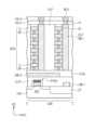
図5、図6A、及び図6Bを参照すれば、基板100はセル領域CAR、コンタクト領域CTR、第1周辺回路領域PER1、及び第2周辺回路領域PER2を含む。コンタクト領域CTRはセル領域CARと第1周辺回路領域PER1との間に介在される。 5, 6A and 6B, the
第1及び第2周辺回路領域PER1、PER2はメモリセルアレイと電気的に連結される周辺トランジスタ、抵抗(resistor)、及びキャパシター(capacitor)を含む。一例として、第1周辺回路領域PER1はセル領域CARのビットラインBLと連結されるセンス増幅器(sense amplifier)を含む。第2周辺回路領域PER2はセル領域CARのワードラインWLと連結されるローデコーダー(row decoder)及び/又はサブワードラインドライバー(sub-word line driver)を含む。 The first and second peripheral circuit regions PER1 and PER2 include peripheral transistors, resistors, and capacitors electrically connected to the memory cell array. For example, the first peripheral circuit area PER1 includes sense amplifiers connected to the bitlines BL of the cell area CAR. The second peripheral circuit area PER2 includes row decoders and/or sub-word line drivers connected to the word lines WL of the cell area CAR.
図6Aを参照すれば、基板100の第1周辺回路領域PER1上に活性領域ACTを定義する素子分離膜STが提供される。活性領域ACT上に、活性領域ACTを横切る周辺ゲート電極PGが提供される。周辺ゲート電極PGの両側の活性領域ACTの上部にソース/ドレイン領域IRが提供される。周辺ゲート電極PGと活性領域ACTとの間に周辺ゲート絶縁膜PGIが介在される。周辺ゲート電極PG上にゲートキャッピング膜PGPが提供される。周辺ゲート電極PGの両側壁上に一対のスペーサーPSPが提供される。第1層間絶縁膜ILD1が活性領域ACT、スペーサーPSP、及びゲートキャッピング膜PGPを覆う。 Referring to FIG. 6A, a device isolation layer ST is provided on the first peripheral circuit region PER1 of the
第1層間絶縁膜ILD1上にセル領域CARに向かう方向に延長される下部配線LMLが提供される。第1層間絶縁膜ILD1を貫通する下部コンタクトLCNTを通じて、下部配線LMLは活性領域ACTのソース/ドレイン領域IRと電気的に連結される。図示しなかったが、下部配線LMLは第1層間絶縁膜ILD1及びゲートキャッピング膜PGPを貫通する下部コンタクトLCNTを通じて周辺ゲート電極PGと電気的に連結されてもよい。第2周辺回路領域PER2上の周辺トランジスタの構造は図6Aに図示された第1周辺回路領域PER1上の周辺トランジスタの構造と実質的に同一である。 A lower interconnection LML extending toward the cell area CAR is provided on the first interlayer dielectric layer ILD1. The lower wiring LML is electrically connected to the source/drain regions IR of the active region ACT through the lower contact LCNT penetrating the first interlayer insulating layer ILD1. Although not shown, the lower line LML may be electrically connected to the peripheral gate electrode PG through a lower contact LCNT penetrating the first interlayer dielectric layer ILD1 and the gate capping layer PGP. The structure of the peripheral transistors on the second peripheral circuit region PER2 is substantially the same as the structure of the peripheral transistors on the first peripheral circuit region PER1 shown in FIG. 6A.
基板100のセル領域CAR及びコンタクト領域CTR上に第1乃至第4積層構造体SS1-SS4が提供される。第1乃至第4積層構造体SS1-SS4は第1層間絶縁膜ILD1上に提供される。第1乃至第4積層構造体SS1-SS4は第1及び第2周辺回路領域PER1、PER2の周辺トランジスタよりさらに高いレベルに位置する。図面を単純化するために、先に図2に図示して説明した半導体パターンSPは省略したまま、第1乃至第4積層構造体SS1-SS4を図示した。 First to fourth stack structures SS1-SS4 are provided on the cell area CAR and the contact area CTR of the
第1乃至第4積層構造体SS1-SS4を覆う第2層間絶縁膜ILD2を貫通して、コンタクト領域CTR上の第1導電ラインCL1と接触するコンタクトCNTが提供される。第1及び第2周辺回路領域PER1、PER2上の第2層間絶縁膜ILD2を貫通して、下部配線LMLと接触するコンタクトCNTが提供される。 A contact CNT is provided to contact the first conductive line CL1 on the contact region CTR through the second interlayer dielectric layer ILD2 covering the first to fourth stacked structures SS1-SS4. A contact CNT is provided through the second interlayer dielectric layer ILD2 on the first and second peripheral circuit regions PER1 and PER2 to contact the lower wiring LML.
コンタクト領域CTRの第1導電ラインCL1と接触するコンタクトCNTは、第1方向D1に配列される。コンタクト領域CTRのコンタクトCNTは第1乃至第4積層構造体SS1-SS4の各々の階段式構造上に配置される。したがって、コンタクト領域CTRのコンタクトCNTはセル領域CARに近くなるほど、その底面のレベルが上昇する。例えば、第1周辺回路領域PER1に近いコンタクトCNTの底面は第1レベルLEV1に位置し、セル領域CARに近いコンタクトCNTの底面は第2レベルLEV2に位置する。第2レベルLEV2は第1レベルLEV1より高い。 The contacts CNT contacting the first conductive lines CL1 of the contact region CTR are arranged in the first direction D1. The contact CNT of the contact region CTR is arranged on the stepped structure of each of the first to fourth stacked structures SS1-SS4. Therefore, the closer the contact CNT of the contact region CTR is to the cell region CAR, the higher the level of its bottom surface. For example, the bottom surface of the contact CNT close to the first peripheral circuit region PER1 is located at the first level LEV1, and the bottom surface of the contact CNT close to the cell area CAR is located at the second level LEV2. The second level LEV2 is higher than the first level LEV1.
第1周辺回路領域PER1の下部配線LMLと接触するコンタクトCNTは、第2方向D2にジグザグ形状に配列される。第1周辺回路領域PER1上のコンタクトCNTがジグザグ形状に配列されることによって、互いに隣接するコンタクトCNTの間の工程マージンを十分に確保することができる。例えば、第1周辺回路領域PER1の第1番目の下部配線LMLは第1端EN1を有する。第1周辺回路領域PER1の第2番目の下部配線LMLは第2端EN2を有する。第2端EN2は第1端EN1に比べてコンタクト領域CTRにさらに近い。第2層間絶縁膜ILD2上に第3及び第4層間絶縁膜ILD3、ILD4が提供される。第3層間絶縁膜ILD3内にビアVIが提供される。第4層間絶縁膜ILD4内に第1乃至第6配線ML1-ML6が提供される。第1乃至第6配線ML1-ML6はビアVIと接触する。 The contacts CNT contacting the lower line LML of the first peripheral circuit region PER1 are arranged in a zigzag shape in the second direction D2. By arranging the contacts CNTs in the zigzag shape on the first peripheral circuit region PER1, a sufficient process margin can be secured between adjacent contact CNTs. For example, the first lower wiring LML of the first peripheral circuit region PER1 has the first end EN1. The second lower wiring LML of the first peripheral circuit region PER1 has a second end EN2. The second end EN2 is closer to the contact region CTR than the first end EN1. Third and fourth interlayer dielectric layers ILD3 and ILD4 are provided on the second interlayer dielectric layer ILD2. A via VI is provided in the third interlayer dielectric layer ILD3. First to sixth wirings ML1-ML6 are provided in the fourth interlayer dielectric layer ILD4. The first to sixth wirings ML1-ML6 are in contact with the via VI.
コンタクト領域CTR上で第1乃至第4配線ML1-ML4はコンタクトCNT及びビアVIを通じて第1乃至第4積層構造体SS1-SS4の第1導電ラインCL1と電気的に連結される。 On the contact region CTR, the first to fourth wirings ML1-ML4 are electrically connected to the first conductive lines CL1 of the first to fourth stack structures SS1-SS4 through contacts CNT and vias VI.
コンタクト領域CTR上で第1配線ML1が第1積層構造体SS1の第1導電ラインCL1と各々接続される。コンタクト領域CTR上で第2配線ML2が第2積層構造体SS2の第1導電ラインCL1と各々接続される。コンタクト領域CTR上で第3配線ML3が第3積層構造体SS3の第1導電ラインCL1と各々接続される。コンタクト領域CTR上で第4配線ML4が第4積層構造体SS4の第1導電ラインCL1と各々接続される。 The first wirings ML1 are connected to the first conductive lines CL1 of the first stacked structure SS1 on the contact regions CTR. The second wirings ML2 are connected to the first conductive lines CL1 of the second stacked structure SS2 on the contact regions CTR. The third wirings ML3 are connected to the first conductive lines CL1 of the third stacked structure SS3 on the contact regions CTR. The fourth wirings ML4 are connected to the first conductive lines CL1 of the fourth stack structure SS4 on the contact regions CTR.
第1配線ML1の数は第1積層構造体SS1の第1導電ラインCL1の数と同一である。第2配線ML2の数は第2積層構造体SS2の第1導電ラインCL1の数と同一である。第3配線ML3の数は第3積層構造体SS3の第1導電ラインCL1の数と同一である。第4配線ML4の数は第4積層構造体SS4の第1導電ラインCL1の数と同一である。 The number of first wirings ML1 is the same as the number of first conductive lines CL1 of the first stacked structural body SS1. The number of second wirings ML2 is the same as the number of first conductive lines CL1 of the second stacked structural body SS2. The number of third wirings ML3 is the same as the number of first conductive lines CL1 of the third stacked structural body SS3. The number of fourth wirings ML4 is the same as the number of first conductive lines CL1 of the fourth stacked structural body SS4.
第1乃至第4配線ML1-ML4の各々は第1方向D1に延在される第1部分と、第2方向D2に延在される第2部分とを含む。例えば、第1配線ML1の第1部分は第2方向D2に一定間隔離隔されて配置される。第1配線ML1の第2部分は第1導電ラインCL1上のコンタクトCNTと連結される。 Each of the first to fourth wirings ML1-ML4 includes a first portion extending in the first direction D1 and a second portion extending in the second direction D2. For example, the first portions of the first wiring ML1 are arranged at regular intervals in the second direction D2. A second portion of the first wiring ML1 is connected to the contact CNT on the first conductive line CL1.
第1乃至第4配線ML1-ML4はコンタクト領域CTRから第1周辺回路領域PER1まで延長される。第1周辺回路領域PER1上で第1乃至第4配線ML1-ML4はコンタクトCNT及びビアVIを通じて下部配線LMLと電気的に連結される。 The first to fourth wirings ML1-ML4 extend from the contact region CTR to the first peripheral circuit region PER1. In the first peripheral circuit region PER1, the first to fourth lines ML1-ML4 are electrically connected to the lower line LML through contacts CNT and vias VI.
セル領域CAR上で第5配線ML5はビアVIを通じて第2導電ラインCL2と電気的に連結される。第5配線ML5は第2方向D2に延在される。第5配線ML5はセル領域CARから第2周辺回路領域PER2まで延長される。第2周辺回路領域PER2上で第5配線ML5はコンタクトCNT及びビアVIを通じて下部配線LMLと電気的に連結される。 In the cell area CAR, the fifth wiring ML5 is electrically connected to the second conductive line CL2 through the via VI. The fifth wiring ML5 extends in the second direction D2. The fifth wiring ML5 extends from the cell area CAR to the second peripheral circuit area PER2. The fifth line ML5 is electrically connected to the lower line LML through the contact CNT and the via VI on the second peripheral circuit region PER2.
第5配線ML5の各々は、第1乃至第4積層構造体SS1-SS4の第2導電ラインCL2と共通に連結される。一例として、第2積層構造体SS2の第1方向D1に配列された第2導電ラインCL2は第1行C1をなす。第3積層構造体SS3の第1方向D1に配列された第2導電ラインCL2は第2行C2をなす。 Each of the fifth lines ML5 is commonly connected to the second conductive lines CL2 of the first to fourth stack structures SS1-SS4. As an example, the second conductive lines CL2 arranged in the first direction D1 of the second stack structure SS2 form a first row C1. The second conductive lines CL2 arranged in the first direction D1 of the third stack structure SS3 form a second row C2.
第1行C1の第1番目の第2導電ラインCL2と第2行C2の第1番目の第2導電ラインCL2とは第2方向D2に整列される。第1行C1の第1番目の第2導電ラインCL2と第2行C2の第1番目の第2導電ラインCL2とは、第1番目の第5配線ML5に共通に連結される。第1行C1の第2番目の第2導電ラインCL2と第2行C2の第2番目の第2導電ラインCL2とは第2方向D2に整列される。第1行C1の第2番目の第2導電ラインCL2と第2行C2の第2番目の第2導電ラインCL2とは、第2番目の第5配線ML5に共通に連結される。 The first second conductive line CL2 of the first row C1 and the first second conductive line CL2 of the second row C2 are aligned in the second direction D2. The first second conductive line CL2 of the first row C1 and the first second conductive line CL2 of the second row C2 are commonly connected to the first fifth wiring ML5. The second second conductive line CL2 of the first row C1 and the second second conductive line CL2 of the second row C2 are aligned in the second direction D2. The second second conductive line CL2 of the first row C1 and the second second conductive line CL2 of the second row C2 are commonly connected to the second fifth wiring ML5.
第1番目の第5配線ML5はセル領域CARの一側に隣接する第2周辺回路領域PER2の上に延長される。第2番目の第5配線ML5はセル領域CARの他側に隣接する第2周辺回路領域PER2の上に延長される。 The first fifth wiring ML5 extends over the second peripheral circuit region PER2 adjacent to one side of the cell region CAR. A second fifth line ML5 extends over a second peripheral circuit region PER2 adjacent to the other side of the cell region CAR.
セル領域CAR上で第6配線ML6はビアVIを通じて第3導電ラインCL3と電気的に連結される。第6配線ML6は第2方向D2に延在される。第6配線ML6は上部ビアUVIを通じて、上位配線(図示せず)と連結される。 In the cell area CAR, the sixth wiring ML6 is electrically connected to the third conductive line CL3 through the via VI. The sixth wiring ML6 extends in the second direction D2. The sixth wiring ML6 is connected to an upper wiring (not shown) through an upper via UVI.
下部配線LML、下部コンタクトLCNT、コンタクトCNT、ビアVI、及び第1乃至第6配線ML1-ML6の各々はアルミニウム、銅、タングステン、モリブデン、及びコバルトの中から選択された少なくとも1つの金属物質を含む。 Each of the lower wiring LML, lower contact LCNT, contact CNT, via VI, and first to sixth wirings ML1-ML6 includes at least one metal material selected from aluminum, copper, tungsten, molybdenum, and cobalt. .
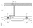
以下、本発明の多様な実施形態に対して説明する。後述する実施形態では、先に図1乃至図6Bを参照して説明したことと重複される技術的特徴に対する詳細な説明は省略し、差異点に対して詳細に説明する。 Various embodiments of the present invention will be described below. In the embodiments described below, detailed descriptions of technical features that are the same as those described with reference to FIGS. 1 to 6B will be omitted, and differences will be described in detail.
図7Aは図5のA-A’線及びB-B’線に沿う断面図である。図7Bは図5のC-C’線に沿う断面図である。図7A及び図7Bを参照すれば、第1及び第2周辺回路領域PER1、PER2上に第1周辺トランジスタPTR1が配置される。さらにコンタクト領域CTR上に少なくとも1つの第2周辺トランジスタPTR2が配置され、セル領域CAR上に少なくとも1つの第3周辺トランジスタPTR3が配置される。 7A is a cross-sectional view taken along lines A-A' and B-B' in FIG. 7B is a cross-sectional view along line C-C' in FIG. 7A and 7B, a first peripheral transistor PTR1 is arranged on the first and second peripheral circuit regions PER1 and PER2. Further, at least one second peripheral transistor PTR2 is arranged on contact region CTR, and at least one third peripheral transistor PTR3 is arranged on cell region CAR.
第2及び第3周辺トランジスタPTR2、PTR3は第1及び第2周辺回路領域PER1、PER2の第1周辺トランジスタPTR1と同一な機能を遂行するトランジスタである。一例として、第2及び第3周辺トランジスタPTR2、PTR3は第1周辺トランジスタPTR1と共にメモリセルを駆動するための周辺回路を構成することができる。本実施形態によれば、周辺回路を構成する周辺トランジスタを第1及び第2周辺回路領域PER1、PER2のみならず、コンタクト領域CTR及びセル領域CAR上にも配置して、周辺トランジスタが形成される面積を相対的に大きく確保することができる。 The second and third peripheral transistors PTR2 and PTR3 are transistors that perform the same function as the first peripheral transistors PTR1 of the first and second peripheral circuit regions PER1 and PER2. For example, the second and third peripheral transistors PTR2 and PTR3 can constitute a peripheral circuit for driving a memory cell together with the first peripheral transistor PTR1. According to the present embodiment, the peripheral transistors forming the peripheral circuit are arranged not only on the first and second peripheral circuit regions PER1 and PER2, but also on the contact region CTR and the cell region CAR to form the peripheral transistors. A relatively large area can be secured.
基板100の素子分離膜ST上に第1下部配線LML1が提供される。第1下部配線LML1はコンタクト領域CTR及びセル領域CAR上に配置される。 A first lower interconnection LML1 is provided on the isolation layer ST of the
第1層間絶縁膜ILD1が第1乃至第3周辺トランジスタPTR1、PTR2、PTR3及び第1下部配線LML1を覆う。第1層間絶縁膜ILD1と第2層間絶縁膜ILD2との間に追加層間絶縁膜ILDaが提供される。追加層間絶縁膜ILDa内に第2下部配線LML2が提供される。 A first interlayer insulating layer ILD1 covers the first to third peripheral transistors PTR1, PTR2 and PTR3 and the first lower interconnection LML1. An additional interlayer dielectric layer ILDa is provided between the first interlayer dielectric layer ILD1 and the second interlayer dielectric layer ILD2. A second lower interconnection LML2 is provided in the additional interlayer insulating layer ILDa.
一例として、第2下部配線LML2は第1層間絶縁膜ILD1を貫通する下部コンタクトLCNTを通じて第2周辺トランジスタPTR2と連結される。結果的に、第1導電ラインCL1が第2周辺トランジスタPTR2と電気的に連結される。 For example, the second lower interconnection LML2 is connected to the second peripheral transistor PTR2 through a lower contact LCNT penetrating the first interlayer dielectric layer ILD1. As a result, the first conductive line CL1 is electrically connected to the second peripheral transistor PTR2.
第1及び第2下部配線LML1、LML2を第1及び第2周辺回路領域PER1、PER2のみならず、コンタクト領域CTR及びセル領域CAR上にも配置して、メモリ素子のルーティング自由度を向上させることができる。さらに、配線が形成される面積を相対的に大きく確保することができる。 The first and second lower wirings LML1 and LML2 are arranged not only on the first and second peripheral circuit regions PER1 and PER2 but also on the contact region CTR and the cell region CAR to improve the routing flexibility of the memory device. can be done. Furthermore, a relatively large area for forming wiring can be ensured.
図8Aは図5のA-A’線及びB-B’線に沿う断面図である。図8Bは図5のC-C’線に沿う断面図である。図8A及び図8Bを参照すれば、第4層間絶縁膜ILD4上に第5層間絶縁膜ILD5及び第6層間絶縁膜ILD6が提供される。第5層間絶縁膜ILD5内に上部ビアUVIが提供される。第6層間絶縁膜ILD6内に上部配線UMLが提供される。上部配線UMLは上部ビアUVIと接触する。上部ビアUVIは上部配線UMLと第1乃至第6配線ML1-ML6を互いに垂直方向で連結する。 8A is a cross-sectional view taken along lines A-A' and B-B' in FIG. 8B is a cross-sectional view along line C-C' in FIG. 8A and 8B, a fifth interlayer dielectric layer ILD5 and a sixth interlayer dielectric layer ILD6 are provided on the fourth interlayer dielectric layer ILD4. An upper via UVI is provided in the fifth interlayer dielectric layer ILD5. An upper wiring UML is provided in the sixth interlayer dielectric layer ILD6. The upper wiring UML makes contact with the upper via UVI. The upper via UVI vertically connects the upper wiring UML and the first to sixth wirings ML1-ML6.
図8Aを参照すれば、第1番目の第4配線ML4は上部配線UMLと電気的に連結される。第1番目の第4配線ML4と連結された上部配線UMLは第1周辺回路領域PER1に延長される。第2番目の第4配線ML4は上部配線UMLと連結されずに、第1周辺回路領域PER1に延長される。第3番目の第4配線ML4は上部配線UMLと電気的に連結される。第3番目の第4配線ML4と連結された上部配線UMLは第1周辺回路領域PER1に延長される。第4番目の第4配線ML4は上部配線UMLと連結されずに、第1周辺回路領域PER1に延長される。 Referring to FIG. 8A, the first fourth wiring ML4 is electrically connected to the upper wiring UML. The upper wiring UML connected to the first fourth wiring ML4 extends to the first peripheral circuit region PER1. The second fourth wiring ML4 extends to the first peripheral circuit region PER1 without being connected to the upper wiring UML. The third fourth wiring ML4 is electrically connected to the upper wiring UML. The upper wiring UML connected to the third fourth wiring ML4 extends to the first peripheral circuit region PER1. The fourth fourth wiring ML4 extends to the first peripheral circuit region PER1 without being connected to the upper wiring UML.
図8Bを参照すれば、第1番目の第5配線ML5は上部配線UMLと電気的に連結される。第1番目の第5配線ML5と連結された上部配線UMLは第2周辺回路領域PER2に延長される。第2番目の第5配線ML5は上部配線UMLと連結されずに、第2周辺回路領域PER2に延長される。 Referring to FIG. 8B, the first fifth wiring ML5 is electrically connected to the upper wiring UML. The upper wiring UML connected to the first fifth wiring ML5 extends to the second peripheral circuit region PER2. The second fifth wiring ML5 extends to the second peripheral circuit region PER2 without being connected to the upper wiring UML.
本実施形態によれば、第1乃至第6配線ML1-ML6上に上位配線である上部配線UMLを追加に配置して、ルーティング自由度を向上させることができる。さらに、配線が形成される面積を相対的に大きく確保することができる。 According to the present embodiment, the upper wirings UML, which are upper wirings, can be additionally arranged on the first to sixth wirings ML1 to ML6 to improve the degree of freedom in routing. Furthermore, a relatively large area for forming wiring can be ensured.
図9は図5のC-C’線に沿う断面図である。図7A及び図9を参照すれば、第1列R1の半導体パターンSPと第2列R2の半導体パターンSPとの間に第2導電ラインCL2及び追加導電ラインCL2aが提供される。再び言えば、垂直方向に積層された半導体パターンSPの両側に第2導電ラインCL2及び追加導電ラインCL2aが配置される。追加導電ラインCL2aは第2導電ラインCL2と平行に第3方向D3に延在される。 FIG. 9 is a cross-sectional view taken along line C-C' of FIG. 7A and 9, a second conductive line CL2 and an additional conductive line CL2a are provided between the semiconductor pattern SP of the first row R1 and the semiconductor pattern SP of the second row R2. In other words, the second conductive line CL2 and the additional conductive line CL2a are disposed on both sides of the vertically stacked semiconductor patterns SP. The additional conductive line CL2a extends in the third direction D3 parallel to the second conductive line CL2.
一例として、追加導電ラインCL2aはメモリセルトランジスタMCTのバックゲート(Back Gate)である。他の例として、追加導電ラインCL2aは第2導電ラインCL2と共に1つのワードラインWLを構成する。その他の例として、追加導電ラインCL2aは半導体パターンSPに直接接触して、ボディーコンタクトの機能を遂行することができる。追加導電ラインCL2aは第1及び第2下部配線LML1、LML2を通じて他の領域と連結される。 As an example, the additional conductive line CL2a is the back gate of the memory cell transistor MCT. As another example, the additional conductive line CL2a constitutes one word line WL together with the second conductive line CL2. As another example, the additional conductive line CL2a may directly contact the semiconductor pattern SP to perform a body contact function. The additional conductive line CL2a is connected to other regions through first and second lower interconnections LML1 and LML2.
図10は図5のA-A’線及びB-B’線に沿う断面図である。図10を参照すれば、第1周辺回路領域PER1の第2層間絶縁膜ILD2上に半導体膜SLが提供される。半導体膜SLは第1乃至第4積層構造体SS1-SS4より高く位置する。半導体膜SL上に周辺トランジスタPTRが形成される。第2周辺回路領域PER2上の周辺トランジスタの構造は図10に図示された第1周辺回路領域PER1上の周辺トランジスタの構造と実質的に同一である。 FIG. 10 is a cross-sectional view taken along lines A-A' and B-B' in FIG. Referring to FIG. 10, a semiconductor layer SL is provided on the second interlayer dielectric layer ILD2 in the first peripheral circuit region PER1. The semiconductor film SL is positioned higher than the first to fourth stacked structures SS1-SS4. A peripheral transistor PTR is formed over the semiconductor film SL. The structure of the peripheral transistors on the second peripheral circuit region PER2 is substantially the same as the structure of the peripheral transistors on the first peripheral circuit region PER1 shown in FIG.
半導体膜SL上に周辺トランジスタPTRを覆う追加層間絶縁膜ILDaが提供される。追加層間絶縁膜ILDaの上面は、コンタクト領域CTR及びセル領域CAR上の第2層間絶縁膜ILD2の上面と実質的に共面をなす。半導体膜SL上の周辺トランジスタPTRは、第1乃至第5配線ML1-ML5を通じて第1及び第2導電ラインCL1、CL2と電気的に連結される。 An additional interlayer insulating layer ILDa is provided on the semiconductor layer SL to cover the peripheral transistor PTR. The top surface of the additional interlayer dielectric ILDa is substantially coplanar with the top surfaces of the second interlayer dielectric ILD2 over the contact region CTR and the cell region CAR. The peripheral transistors PTR on the semiconductor layer SL are electrically connected to the first and second conductive lines CL1 and CL2 through the first to fifth wirings ML1-ML5.
図11は本発明の実施形態に係る3次元半導体メモリ素子を示す斜視図である。図12は図5のA-A’線に沿う断面図である。図11及び図12を参照すれば、第1周辺回路領域PER1は第1サブ領域PER1a及び第2サブ領域PER1bを含む。第2サブ領域PER1bは第1サブ領域PER1aと第1方向D1に離隔される。第1及び第2サブ領域PER1a、PER1b上に第1及び第2周辺トランジスタPTR1、PTR2が各々提供される。 FIG. 11 is a perspective view showing a 3D semiconductor memory device according to an embodiment of the present invention. FIG. 12 is a cross-sectional view along line A-A' in FIG. 11 and 12, the first peripheral circuit region PER1 includes a first sub-region PER1a and a second sub-region PER1b. The second sub-region PER1b is separated from the first sub-region PER1a in the first direction D1. First and second peripheral transistors PTR1 and PTR2 are provided on the first and second sub-regions PER1a and PER1b, respectively.
例えば、第1番目の第4配線ML4は第1サブ領域PER1aに延長される。第2番目の第4配線ML4は第2サブ領域PER1bに延長される。第3番目の第4配線ML4は第1サブ領域PER1aに延長される。第4番目の第4配線ML4は第2サブ領域PER1bに延長される。 For example, the first fourth wiring ML4 extends to the first sub-region PER1a. The second fourth line ML4 extends to the second sub-region PER1b. The third fourth wiring ML4 extends to the first sub-region PER1a. The fourth fourth wiring ML4 extends to the second sub-region PER1b.
本実施形態によれば、第1周辺回路領域PER1を2つの区域に分割して第1及び第2サブ領域PER1a、PER1bを構成する。したがって、第1周辺回路領域PER1の周辺回路を構成する第1及び第2周辺トランジスタPTR1、PTR2を各々第1及び第2サブ領域PER1a、PER1bに分けて配置する。結果的に、周辺トランジスタが形成される面積を相対的に大きく確保することができ、隣接するコンタクトCNTの間の間隔も相対的に大きく確保することができる。 According to the present embodiment, the first peripheral circuit region PER1 is divided into two regions to form first and second sub-regions PER1a and PER1b. Accordingly, the first and second peripheral transistors PTR1 and PTR2 forming the peripheral circuit of the first peripheral circuit region PER1 are divided into the first and second sub-regions PER1a and PER1b, respectively. As a result, a relatively large area for forming the peripheral transistor can be secured, and a relatively large interval between adjacent contact CNTs can be secured.
図13は本発明の実施形態に係る3次元半導体メモリ素子を示す斜視図である。図13を参照すれば、第1周辺回路領域PER1が複数に提供される。例えば、第1周辺回路領域PER1はセンス増幅器を含む。 FIG. 13 is a perspective view showing a 3D semiconductor memory device according to an embodiment of the present invention. Referring to FIG. 13, a plurality of first peripheral circuit regions PER1 are provided. For example, the first peripheral circuit region PER1 includes sense amplifiers.
セル領域CARの一側に隣接して、第1周辺回路領域PER1と第2周辺回路領域PER2とが第1方向D1に沿って互いに交互に配列される。セル領域CARの他側に隣接して、第1周辺回路領域PER1と第2周辺回路領域PER2とが第1方向D1に沿って互いに交互に配列される。 Adjacent to one side of the cell area CAR, the first peripheral circuit area PER1 and the second peripheral circuit area PER2 are alternately arranged along the first direction D1. Adjacent to the other side of the cell area CAR, the first peripheral circuit area PER1 and the second peripheral circuit area PER2 are alternately arranged along the first direction D1.
図14は本発明の実施形態に係る3次元半導体メモリ素子を示す斜視図である。図14を参照すれば、第1周辺回路領域PER1は第2方向D2に延在される第1部分PA1及び第1部分PA1から第1方向D1に延在される第2部分PA2を含む。 FIG. 14 is a perspective view of a 3D semiconductor memory device according to an embodiment of the present invention. Referring to FIG. 14, the first peripheral circuit region PER1 includes a first portion PA1 extending in the second direction D2 and a second portion PA2 extending in the first direction D1 from the first portion PA1.
図13及び図14を参照して説明した実施形態によれば、先に図5を参照して説明した第1周辺回路領域PER1の面積に比べて第1周辺回路領域PER1の面積をより広く確保する。 According to the embodiments described with reference to FIGS. 13 and 14, the area of the first peripheral circuit region PER1 is secured larger than the area of the first peripheral circuit region PER1 described with reference to FIG. do.
図15は本発明の実施形態に係る3次元半導体メモリ素子を示す斜視図である。図16は図15のA-A’線に沿う断面図である。図15及び図16を参照すれば、コンタクト領域CTR上に第1導電ラインCL1と接触する共通コンタクトCCNTが提供される。共通コンタクトCCNTの各々は互いに同一なレベルに位置する一対の第1導電ラインCL1と共通に接触する。 FIG. 15 is a perspective view showing a 3D semiconductor memory device according to an embodiment of the present invention. 16 is a cross-sectional view taken along the line A-A' in FIG. 15. FIG. 15 and 16, a common contact CCNT is provided on the contact region CTR and contacts the first conductive line CL1. Each common contact CCNT is in common contact with a pair of first conductive lines CL1 located at the same level.
例えば、第2積層構造体SS2の最下部の第1導電ラインCL1と第3積層構造体SS3の最下部の第1導電ラインCL1は、1つの共通コンタクトCCNTに共通に連結される。第2積層構造体SS2の最上部の第1導電ラインCL1と第3積層構造体SS3の最上部の第1導電ラインCL1は、1つの共通コンタクトCCNTに共通に連結される。 For example, the bottom first conductive line CL1 of the second stack structure SS2 and the bottom first conductive line CL1 of the third stack structure SS3 are commonly connected to one common contact CCNT. The top first conductive line CL1 of the second stack structure SS2 and the top first conductive line CL1 of the third stack structure SS3 are commonly connected to one common contact CCNT.
先に図5の第1乃至第4配線ML1-ML4の代わりに共通配線CMLが提供される。共通配線CMLはビアVIを通じて共通コンタクトCCNTと電気的に連結される。共通配線CMLの各々は互いに同一なレベルに位置する一対の第1導電ラインCL1と電気的に連結される。 A common line CML is provided instead of the first to fourth lines ML1-ML4 of FIG. The common line CML is electrically connected to the common contact CCNT through vias VI. Each of the common lines CML is electrically connected to a pair of first conductive lines CL1 located at the same level.
図示しなかったが、本発明の他の実施形態において、共通コンタクトCCNTは、第1積層構造体SS1の第1導電ラインCL1及び第2積層構造体SS2の第1導電ラインCL1と共通に接触するように提供される。共通コンタクトCCNTは、第3積層構造体SS3の第1導電ラインCL1及び第4積層構造体SS4の第1導電ラインCL1と共通に接触するように提供される。 Although not shown, in another embodiment of the present invention, the common contact CCNT is in common contact with the first conductive line CL1 of the first stack structure SS1 and the first conductive line CL1 of the second stack structure SS2. provided as A common contact CCNT is provided to be in common contact with the first conductive line CL1 of the third stack structure SS3 and the first conductive line CL1 of the fourth stack structure SS4.
第5配線ML5は第1サブ配線ML5a及び第2サブ配線ML5bを含む。第1サブ配線ML5a及び第2サブ配線ML5bは第1方向D1に沿って互いに交互に配列される。各々の第1サブ配線ML5aは第2及び第4積層構造体SS2、SS4の第2導電ラインCL2と共通に連結される。各々の第1サブ配線ML5aは第1及び第3積層構造体SS1、SS3の第2導電ラインCL2とは連結されない。各々の第2サブ配線ML5bは第1及び第3積層構造体SS1、SS3の第2導電ラインCL2と共通に連結される。各々の第2サブ配線ML5bは第2及び第4積層構造体SS2、SS4の第2導電ラインCL2とは連結されない。 The fifth wiring ML5 includes a first sub-wiring ML5a and a second sub-wiring ML5b. The first sub-wirings ML5a and the second sub-wirings ML5b are alternately arranged along the first direction D1. Each first sub-line ML5a is commonly connected to the second conductive lines CL2 of the second and fourth stack structures SS2 and SS4. Each first sub-line ML5a is not connected to the second conductive lines CL2 of the first and third stack structures SS1 and SS3. Each second sub-line ML5b is commonly connected to the second conductive lines CL2 of the first and third stacked structures SS1 and SS3. Each second sub-line ML5b is not connected to the second conductive lines CL2 of the second and fourth stack structures SS2 and SS4.
一例として、第2積層構造体SS2の第2導電ラインCL2は第1行C1をなし、第3積層構造体SS3の第2導電ラインCL2は第2行C2をなす。第1行C1の第1番目の第2導電ラインCL2と第2行C2の第1番目の第2導電ラインCL2は第2方向D2に整列されず、互いにオフセットされる。第1行C1の第1番目の第2導電ラインCL2は第1サブ配線ML5aと電気的に連結され、第2行C2の第1番目の第2導電ラインCL2は第2サブ配線ML5bと電気的に連結される。第1行C1の第2番目の第2導電ラインCL2と第2行C2の第2番目の第2導電ラインCL2とは第2方向D2に整列されず、互いにオフセットされる。第1行C1の第2番目の第2導電ラインCL2は第1サブ配線ML5aと電気的に連結され、第2行C2の第2番目の第2導電ラインCL2は第2サブ配線ML5bと電気的に連結される。 As an example, the second conductive lines CL2 of the second stack structure SS2 form the first row C1, and the second conductive lines CL2 of the third stack structure SS3 form the second row C2. The first second conductive line CL2 of the first row C1 and the first second conductive line CL2 of the second row C2 are not aligned in the second direction D2 and are offset from each other. The first second conductive line CL2 of the first row C1 is electrically connected to the first sub-line ML5a, and the first second conductive line CL2 of the second row C2 is electrically connected to the second sub-line ML5b. connected to The second second conductive line CL2 of the first row C1 and the second second conductive line CL2 of the second row C2 are not aligned in the second direction D2 and are offset from each other. The second second conductive line CL2 of the first row C1 is electrically connected to the first sub-line ML5a, and the second second conductive line CL2 of the second row C2 is electrically connected to the second sub-line ML5b. connected to
第1サブ配線ML5aはセル領域CARからセル領域CARの一側に隣接する第2周辺回路領域PER2の上に延長される。第2サブ配線ML5bはセル領域CARからセル領域CARの他側に隣接する第2周辺回路領域PER2の上に延長される。 The first sub-line ML5a extends from the cell area CAR onto the second peripheral circuit area PER2 adjacent to one side of the cell area CAR. The second sub-line ML5b extends from the cell area CAR onto the second peripheral circuit area PER2 adjacent to the other side of the cell area CAR.
第2周辺回路領域PER2の下部配線LMLと接触するコンタクトCNTは、第2方向D2にジグザグ形状に配列される。第2周辺回路領域PER2上のコンタクトCNTがジグザグ形状に配列されることによって、互いに隣接するコンタクトCNTの間の工程マージンを十分に確保することができる。例えば、第2周辺回路領域PER2の第1番目の下部配線LMLは第1端EN1を有する。第2周辺回路領域PER2の第2番目の下部配線LMLは第2端EN2を有する。第2端EN2は第1端EN1に比べてコンタクト領域CTRにさらに近い。 The contacts CNT contacting the lower wiring LML of the second peripheral circuit region PER2 are arranged in a zigzag shape in the second direction D2. By arranging the contacts CNTs on the second peripheral circuit region PER2 in a zigzag shape, a sufficient process margin can be secured between adjacent contact CNTs. For example, the first lower wiring LML of the second peripheral circuit region PER2 has the first end EN1. The second lower wiring LML of the second peripheral circuit region PER2 has a second end EN2. The second end EN2 is closer to the contact region CTR than the first end EN1.
図17は本発明の実施形態に係る3次元半導体メモリ素子を示す斜視図である。図18は図17のA-A’線及びB-B’線に沿う断面図である。図17及び図18を参照すれば第1導電ラインCL1の各々は第1方向D1に延在される配線部LP及び配線部LPから第3方向D3に延在されるコンタクト部CNPを含む。 FIG. 17 is a perspective view showing a 3D semiconductor memory device according to an embodiment of the present invention. 18 is a cross-sectional view taken along lines A-A' and B-B' of FIG. 17. FIG. 17 and 18, each of the first conductive lines CL1 includes a wiring portion LP extending in the first direction D1 and a contact portion CNP extending from the wiring portion LP in the third direction D3.
第1導電ラインCL1のコンタクト部CNPはコンタクト領域CTR上に配置される。第1乃至第4積層構造体SS1-SS4の各々のコンタクト部CNPは、第1方向D1に配列される。コンタクト部CNPの上面は第2層間絶縁膜ILD2の上面と実質的に共面をなす。コンタクト部CNPの上面上にビアVIが配置される。コンタクト部CNPはビアVIを通じて第1乃至第4配線ML1-ML4と電気的に連結される。 A contact portion CNP of the first conductive line CL1 is disposed on the contact region CTR. The contact portions CNP of each of the first to fourth stacked structural bodies SS1-SS4 are arranged in the first direction D1. The top surface of the contact portion CNP is substantially coplanar with the top surface of the second interlayer dielectric film ILD2. A via VI is arranged on the upper surface of the contact portion CNP. The contact part CNP is electrically connected to the first to fourth lines ML1-ML4 through vias VI.
以上、添付された図面を参照して本発明の実施形態を説明したが、本発明はその技術的思想や必須的な特徴を変形しなく、他の具体的な形態に実施されることもあり得る。したがって、以上で記述した実施形態はすべての面で例示的なものであり、限定的なものではないものとして理解しなければならない。 Although the embodiments of the present invention have been described above with reference to the accompanying drawings, the present invention may be implemented in other specific forms without changing its technical idea or essential features. obtain. Accordingly, the embodiments described above are to be considered in all respects as illustrative and not restrictive.
100 基板
ACT 活性領域
CAR セル領域
CH チャネル領域
CL1、CL2 導電ライン
CNT コンタクト
CTR コンタクト領域
DL 誘電膜
DS 情報格納要素
EL1、EL2 電極
GI ゲート絶縁膜
IL 絶縁膜
ILD1~ILD6 層間絶縁膜
IR ソース/ドレイン領域
LCNT 下部コンタクト
MCT メモリセルトランジスタ
ML1~ML6 配線
PER1、PER2 周辺回路領域
PG 周辺ゲート電極
PGI 周辺ゲート絶縁膜
PGP ゲートキャッピング膜
PP 接地配線
PSP スペーサー
PTR1~PTR4 周辺トランジスタ
SC シリサイド膜
SCA サブセルアレイ
SD1、SD2 不純物領域
SG 終端膜
SL 半導体膜
SP 半導体パターン
SS1-SS4 積層構造体
ST 素子分離膜
VI ビア
VIP 垂直絶縁パターン
WL ワードライン100 substrate ACT active region CAR cell region CH channel region CL1, CL2 conductive line CNT contact CTR contact region DL dielectric film DS information storage elements EL1, EL2 electrode GI gate insulating film IL insulating films ILD1 to ILD6 interlayer insulating film IR source/drain regions LCNT Lower contact MCT Memory cell transistors ML1 to ML6 Wiring PER1, PER2 Peripheral circuit region PG Peripheral gate electrode PGI Peripheral gate insulating film PGP Gate capping film PP Ground wiring PSP Spacers PTR1 to PTR4 Peripheral transistor SC Silicide film SCA Sub-cell arrays SD1, SD2 Impurities Region SG Termination film SL Semiconductor film SP Semiconductor patterns SS1 to SS4 Laminated structure ST Element isolation film VI Via VIP Vertical insulation pattern WL Word line
Claims (14)
Translated fromJapanese前記第1及び第2積層構造体上の第1配線及び第2配線と、を含み、
前記第1及び第2積層構造体の各々は、
垂直方向に積層された複数の半導体パターンであり、各々が、前記第1方向と交差する第2方向に延在される複数の半導体パターンと、
垂直方向に積層されて前記複数の半導体パターンと連結された複数の導電ラインであり、各々が前記第1方向に延在される複数の導電ラインと、
前記複数の半導体パターンと隣接して垂直方向に延在されるゲート電極と、を含み、
前記第1積層構造体の前記複数の導電ラインは、第1導電ラインを含み、
前記第2積層構造体の前記複数の導電ラインは、前記第1導電ラインと同一なレベルに位置する第2導電ラインを含み、
前記第1配線は、前記第1及び第2導電ラインのうちの少なくとも1つと電気的に連結され、前記基板の外周部に向かって前記第1方向に引き出され、
前記第2配線は、前記第1及び第2積層構造体の前記ゲート電極のうちの少なくとも1つと電気的に連結され、前記基板の外周部に向かって前記第2方向に引き出される、半導体メモリ素子。a first laminated structure and a second laminated structure on the substrate, the first laminated structure and the second laminated structure extending in a first direction parallel to each other;
a first wiring and a second wiring on the first and second laminated structures;
Each of the first and second laminated structures,
a plurality of verticallystacked semiconductor patterns each extending in a second direction crossing the first direction ;
a pluralityofconductive linesvertically stacked and connected tothe plurality of semiconductor patterns,each conductive line extending in the first direction ;
a vertically extending gate electrode adjacent tothe plurality of semiconductor patterns;
the plurality of conductive lines of the first laminated structure includes a first conductive line;
the plurality of conductive lines of the second stacked structure includes a second conductive line located at the same level as the first conductive line;
the first wiring is electrically connected to at least one of the first and second conductive lines andextends in the first direction toward an outer periphery of the substrate;
The semiconductor memory, wherein the second wiring is electrically connected to at least one of the gate electrodes of the first and second stacked structuresand is drawn out in the second direction toward the outer periphery of the substrate. element.
前記第1配線は、前記第1導電ラインと電気的に連結され、
前記第3配線は、前記第2導電ラインと電気的に連結され、
前記第2配線は、前記第1及び第2積層構造体の前記ゲート電極と共通に連結される、請求項1に記載の半導体メモリ素子。further comprising third wiring on the first and second laminated structures;
the first wiring is electrically connected to the first conductive line;
the third wiring is electrically connected to the second conductive line;
2. The semiconductor memory device of claim 1, wherein the second line is commonly connected to the gate electrodes of the first and second stack structures.
前記第2配線と共通に連結される前記ゲート電極は、前記第2方向に整列される、請求項2に記載の半導体メモリ素子。the second wiring extends inthe second direction;
3. The semiconductor memory device of claim 2, wherein the gate electrodes commonly connected to the second line are aligned in thesecond direction.
前記第1配線は、前記第1及び第2導電ラインと共通に連結され、
前記第2配線は、前記第1積層構造体の前記ゲート電極と電気的に連結され、
前記第3配線は、前記第2積層構造体の前記ゲート電極と電気的に連結される、請求項1に記載の半導体メモリ素子。further comprising third wiring on the first and second laminated structures;
the first wiring is commonly connected to the first and second conductive lines;
the second wiring is electrically connected to the gate electrode of the first stacked structure;
2. The semiconductor memory device of claim 1, wherein the third line is electrically connected to the gate electrode of the second stack structure.
前記第1配線は、前記共通コンタクトと電気的に連結される、請求項4に記載の半導体メモリ素子。further comprising a common contact in common contact with the first and second conductive lines;
5. The semiconductor memory device of claim 4, wherein the first line is electrically connected to the common contact.
前記導電ラインの各々は、前記半導体パターンの各々の前記第1不純物領域と電気的に連結され、
前記ゲート電極の各々は、前記半導体パターンの前記チャネル領域に隣接する、請求項1に記載の半導体メモリ素子。each of the semiconductor patterns includes a first impurity region, a second impurity region, and a channel region interposed between the first and second impurity regions;
each of the conductive lines is electrically connected to the first impurity region of each of the semiconductor patterns;
2. The semiconductor memory device of claim 1, wherein each of said gate electrodes is adjacent to said channel region of said semiconductor pattern.
前記終端膜は、前記チャネル領域の半導体元素より狭いバンドギャップを有する半導体元素を含む、請求項6に記載の半導体メモリ素子。each of the semiconductor patterns further comprising a termination layer interposed between the first impurity region and the conductive line;
7. The semiconductor memory device of claim 6, wherein the termination layer comprises a semiconductor element having a narrower bandgap than the semiconductor element of the channel region.
前記第1配線は、前記第1方向に前記第1周辺回路領域に向かって延在されて、前記第1周辺回路領域上の第1周辺トランジスタと電気的に連結され、
前記第2配線は、前記第2方向に前記第2周辺回路領域に向かって延在されて、前記第2周辺回路領域上の第2周辺トランジスタと電気的に連結される、請求項1に記載の半導体メモリ素子。the outer peripheral portion of the substrate includes a first peripheral circuit area and a second peripheral circuit area;
the first wiringextends in thefirst direction toward the first peripheral circuit region and is electrically connected to a first peripheral transistor on the first peripheral circuit region;
2. The second wiring of claim 1,wherein the second wiringextends in the second direction toward the second peripheral circuit region and is electrically connected to a second peripheral transistor on the second peripheral circuit region. semiconductor memory device.
前記基板は、セル領域及びコンタクト領域を含み、
前記第1及び第2積層構造体の前記導電ラインは、前記セル領域から前記コンタクト領域に延長され、
前記コンタクトは、前記コンタクト領域上に配置され、
前記第1配線は、前記コンタクトと電気的に連結される、請求項1に記載の半導体メモリ素子。further comprising a contact contacting at least one of the first and second conductive lines;
the substrate includes a cell area and a contact area;
the conductive lines of the first and second stack structures extend from the cell area to the contact area;
the contact is disposed on the contact region;
2. The semiconductor memory device of claim 1, wherein the first wiring is electrically connected to the contact.
前記第1及び第2積層構造体の前記導電ラインの各々は、
前記セル領域から前記コンタクト領域に水平方向に延在される配線部と、
前記コンタクト領域上で前記配線部から垂直方向に延在されるコンタクト部と、を含み、
前記第1配線は、前記第1及び第2導電ラインの前記コンタクト部のうちの少なくとも1つと電気的に連結される、請求項1に記載の半導体メモリ素子。the substrate includes a cell area and a contact area;
each of the conductive lines of the first and second laminate structures comprising:
a wiring portion horizontally extending from the cell region to the contact region;
a contact portion extending vertically from the wiring portion on the contact region;
2. The semiconductor memory device of claim 1, wherein the first wiring is electrically connected to at least one of the contact portions of the first and second conductive lines.
前記セル領域上で垂直方向に積層され、第1方向に延在される複数の半導体パターンであり、各々が第1不純物領域、第2不純物領域、及び前記第1及び第2不純物領域の間のチャネル領域を含む複数の半導体パターンと、
垂直方向に積層され、前記複数の半導体パターンの前記第1不純物領域と連結される複数の第1導電ラインであり、前記セル領域から前記コンタクト領域に、前記第1方向と交差する第2方向に延長された複数の第1導電ラインと、
前記複数の半導体パターンの各々の前記第2不純物領域と連結されるキャパシターと、
前記コンタクト領域上の前記複数の第1導電ラインと接触する複数のコンタクトであり、前記第2方向に整列された複数のコンタクトと、
前記複数のコンタクトと電気的に連結される複数の配線と、を含み、
前記複数のコンタクトは、第1コンタクト及び前記第1コンタクトより前記セル領域にさらに近い第2コンタクトを含み、
前記第2コンタクトの底面のレベルは、前記第1コンタクトの底面のレベルより高く、
前記複数の配線は、それぞれ前記第1コンタクト及び前記第2コンタクトと電気的に連結される第1配線及び第2配線を含み、
前記第1配線及び第2配線は、前記基板の外周部に向かって前記第2方向に引き出される、半導体メモリ素子。a substrate including cell regions and contact regions;
a plurality of semiconductor patterns stacked vertically onthe cell regionand extending in a first direction, each of which includes a first impurity region, a second impurity region, and between the first and second impurity regions; a plurality of semiconductor patterns including channel regions of
a plurality of first conductive lines vertically stacked and connected to the first impurity regions of the plurality of semiconductor patterns, extending from the cell region to the contact region in a second direction crossing the first direction;a plurality of elongated first conductive lines ;
a capacitor connected to the second impurity regionof each ofthe plurality of semiconductor patterns;
a plurality of contacts in contact withthe plurality of first conductive lines on the contact regionand aligned in the second direction ;
a plurality of wires electrically connected to the plurality of contacts,
the plurality of contacts includes a first contact and a second contact closer to the cell region than the first contact;
the level of the bottom surface of the second contactis higher than the level of the bottom surface of the first contact;
the plurality of wires includes a first wire and a second wire electrically connected to the first contact and the second contact, respectively;
The semiconductor memory device, wherein the first wiring and the second wiring are drawn out in the second direction toward the outer periphery of the substrate .
前記第2コンタクトと接触する前記第1導電ラインは、前記コンタクト領域上で第2長さを有し、
前記第1長さは、前記第2長さより大きい、請求項11に記載の半導体メモリ素子。said first conductive line contacting said first contact having a first length over said contact area;
said first conductive line contacting said second contact having a second length over said contact area;
12. The semiconductor memory device of claim11 , wherein the first length is greater than the second length.
前記第1及び第2下部配線は、それぞれ、前記第1配線及び前記第2配線と電気的に連結され、
前記第1及び第2下部配線は、各々第1端及び第2端を含み、
前記第2端は、前記第1端より前記コンタクト領域に近い、請求項11に記載の半導体メモリ素子。further comprising a first lower wiring and a second lower wiring on a peripheral circuit area ofthe substrate;
the first and second lower wirings areelectrically connected to the firstwiring and thesecond wiring,respectively ;
the first and second lower interconnections each include a first end and a second end;
12. The semiconductor memory device of claim11 , wherein said second end is closer to said contact region than said first end.
前記第2導電ラインと電気的に連結される第3配線と、をさらに含み、
前記基板は、第1及び第2周辺回路領域をさらに含み、
前記第1及び第2配線は、前記第1周辺回路領域の上に延長され、前記第3配線は、前記第2周辺回路領域の上に延長される、請求項11に記載の半導体メモリ素子。a second conductive line extending vertically adjacent to the channel region ofeach ofthe plurality of semiconductor patterns;
athird wiring electrically connected to thesecond conductive line;
the substrate further includes first and second peripheral circuit regions;
12. The semiconductor memory according to claim11 , wherein said first and second wiringsextend over saidfirst peripheral circuit region, and said third wiring extends over said second peripheral circuit region. element.
Applications Claiming Priority (4)
| Application Number | Priority Date | Filing Date | Title |
|---|---|---|---|
| US201862629335P | 2018-02-12 | 2018-02-12 | |
| US62/629,335 | 2018-02-12 | ||
| KR1020180058523AKR102494114B1 (en) | 2018-02-12 | 2018-05-23 | Semiconductor memory device |
| KR10-2018-0058523 | 2018-05-23 |
Publications (2)
| Publication Number | Publication Date |
|---|---|
| JP2019140382A JP2019140382A (en) | 2019-08-22 |
| JP7338975B2true JP7338975B2 (en) | 2023-09-05 |
Family
ID=65279422
Family Applications (1)
| Application Number | Title | Priority Date | Filing Date |
|---|---|---|---|
| JP2019004399AActiveJP7338975B2 (en) | 2018-02-12 | 2019-01-15 | semiconductor memory device |
Country Status (4)
| Country | Link |
|---|---|
| US (2) | US10910378B2 (en) |
| EP (1) | EP3534401B1 (en) |
| JP (1) | JP7338975B2 (en) |
| CN (1) | CN110164867B (en) |
Families Citing this family (29)
| Publication number | Priority date | Publication date | Assignee | Title |
|---|---|---|---|---|
| KR102639721B1 (en)* | 2018-04-13 | 2024-02-26 | 삼성전자주식회사 | Three-dimensional semiconductor memory devices |
| KR102634614B1 (en)* | 2019-07-12 | 2024-02-08 | 에스케이하이닉스 주식회사 | Vertical memory device |
| KR102749009B1 (en)* | 2019-08-30 | 2025-01-02 | 삼성전자주식회사 | Integrated circuit device |
| JP2021048298A (en)* | 2019-09-19 | 2021-03-25 | キオクシア株式会社 | Semiconductor storage device and manufacturing method of semiconductor storage device |
| US11239238B2 (en) | 2019-10-29 | 2022-02-01 | Intel Corporation | Thin film transistor based memory cells on both sides of a layer of logic devices |
| US11335686B2 (en) | 2019-10-31 | 2022-05-17 | Intel Corporation | Transistors with back-side contacts to create three dimensional memory and logic |
| KR102759369B1 (en) | 2019-11-11 | 2025-01-24 | 삼성전자주식회사 | Integrated circuit device and method of manufacturing the same |
| US11257822B2 (en)* | 2019-11-21 | 2022-02-22 | Intel Corporation | Three-dimensional nanoribbon-based dynamic random-access memory |
| KR102741107B1 (en) | 2019-11-22 | 2024-12-10 | 삼성전자주식회사 | Semiconductor memory device and method of manufacturing the same |
| US11056492B1 (en) | 2019-12-23 | 2021-07-06 | Intel Corporation | Dense memory arrays utilizing access transistors with back-side contacts |
| KR102671791B1 (en)* | 2020-01-13 | 2024-06-04 | 에스케이하이닉스 주식회사 | Semiconductor device and manufacturing method thereof |
| KR102736068B1 (en) | 2020-01-31 | 2024-12-02 | 에스케이하이닉스 주식회사 | Memory device |
| US11087832B1 (en) | 2020-03-02 | 2021-08-10 | Intel Corporation | Three-dimensional nanoribbon-based static random-access memory |
| US11094699B1 (en)* | 2020-05-28 | 2021-08-17 | Micron Technology, Inc. | Apparatuses including stacked horizontal capacitor structures and related methods, memory devices, and electronic systems |
| KR102747694B1 (en) | 2020-08-25 | 2024-12-30 | 삼성전자주식회사 | Three dimensional semiconductor memory device |
| KR102780920B1 (en)* | 2020-09-02 | 2025-03-12 | 양쯔 메모리 테크놀로지스 씨오., 엘티디. | Method for forming on-chip capacitor structures in semiconductor devices |
| JP2022147872A (en) | 2021-03-23 | 2022-10-06 | キオクシア株式会社 | semiconductor storage device |
| US12412835B2 (en) | 2021-04-27 | 2025-09-09 | Intel Corporation | Back-side power delivery with glass support at the front |
| KR20220168884A (en) | 2021-06-17 | 2022-12-26 | 삼성전자주식회사 | Semiconductor memory devices |
| JP2023001826A (en) | 2021-06-21 | 2023-01-06 | キオクシア株式会社 | semiconductor storage device |
| KR20230004039A (en)* | 2021-06-30 | 2023-01-06 | 에스케이하이닉스 주식회사 | Semiconductor memory device |
| CN115020480A (en) | 2022-05-31 | 2022-09-06 | 长鑫存储技术有限公司 | Semiconductor structure |
| US20230389281A1 (en)* | 2022-05-31 | 2023-11-30 | Changxin Memory Technologies, Inc. | Semiconductor structure and manufacturing method thereof |
| CN115117017A (en) | 2022-06-15 | 2022-09-27 | 长鑫存储技术有限公司 | semiconductor structure |
| CN117334668A (en) | 2022-06-16 | 2024-01-02 | 长鑫存储技术有限公司 | Semiconductor structure and preparation method thereof |
| CN117352489A (en)* | 2022-06-21 | 2024-01-05 | 长鑫存储技术有限公司 | Semiconductor structure, manufacturing method thereof, memory chip and electronic equipment |
| CN117545270A (en)* | 2022-07-27 | 2024-02-09 | 长鑫存储技术有限公司 | Semiconductor structure and forming method thereof |
| CN118338646A (en)* | 2023-01-03 | 2024-07-12 | 长鑫存储技术有限公司 | Semiconductor structure and method of forming the same |
| KR20250139489A (en)* | 2024-03-15 | 2025-09-23 | 삼성전자주식회사 | Semiconductor device |
Citations (5)
| Publication number | Priority date | Publication date | Assignee | Title |
|---|---|---|---|---|
| JP2003124476A (en) | 1994-09-13 | 2003-04-25 | Toshiba Corp | Semiconductor device and manufacturing method thereof |
| US20120231619A1 (en) | 2011-03-08 | 2012-09-13 | Samsung Electronics Co., Ltd. | Method of fabricating and semiconductor memory device using the same |
| JP2016526782A (en) | 2013-07-01 | 2016-09-05 | マイクロン テクノロジー, インク. | Semiconductor device including staircase structure and related method |
| US20170053906A1 (en) | 2015-08-23 | 2017-02-23 | Monolithic 3D Inc. | Semiconductor memory device and structure |
| US20170117291A1 (en) | 2015-10-24 | 2017-04-27 | Monolithic 3D Inc. | Semiconductor memory device, structure and methods |
Family Cites Families (20)
| Publication number | Priority date | Publication date | Assignee | Title |
|---|---|---|---|---|
| TW406419B (en)* | 1998-01-15 | 2000-09-21 | Siemens Ag | Memory-cells arrangement and its production method |
| JP2003234419A (en)* | 2002-02-08 | 2003-08-22 | Mitsubishi Electric Corp | Semiconductor device manufacturing method and semiconductor device manufactured by the method |
| KR100476694B1 (en)* | 2002-11-07 | 2005-03-17 | 삼성전자주식회사 | structure of a Fuse for a semiconductor device and method of manufacturing the same |
| US20050275006A1 (en) | 2004-05-25 | 2005-12-15 | Ming Tang | [multi-gate dram with deep-trench capacitor and fabrication thereof] |
| KR100688554B1 (en)* | 2005-06-23 | 2007-03-02 | 삼성전자주식회사 | Semiconductor Memory Devices Including Power Decoupling Capacitors |
| KR101527193B1 (en)* | 2008-12-10 | 2015-06-08 | 삼성전자주식회사 | Semiconductor device and its cell block arrangement method |
| US8773881B2 (en)* | 2009-03-10 | 2014-07-08 | Contour Semiconductor, Inc. | Vertical switch three-dimensional memory array |
| KR20120092483A (en) | 2011-02-11 | 2012-08-21 | 삼성전자주식회사 | Three dimensional semiconductor memory device and method of forming the same |
| US8357964B1 (en) | 2011-09-07 | 2013-01-22 | Rexchip Electronics Corporation | Three-dimensional dynamic random access memory with an ancillary electrode structure |
| US9023723B2 (en) | 2012-05-31 | 2015-05-05 | Applied Materials, Inc. | Method of fabricating a gate-all-around word line for a vertical channel DRAM |
| KR20140026894A (en) | 2012-08-23 | 2014-03-06 | 에스케이하이닉스 주식회사 | 3 dimension stack memory device |
| US8902663B1 (en) | 2013-03-11 | 2014-12-02 | Monolithic 3D Inc. | Method of maintaining a memory state |
| US9570459B2 (en)* | 2013-07-10 | 2017-02-14 | Unity Semiconductor Corporation | Vertical gate NAND memory devices |
| CH708282A1 (en)* | 2013-07-10 | 2015-01-15 | Capartis Ag | Plastic containers with screw cap. |
| US20150019802A1 (en) | 2013-07-11 | 2015-01-15 | Qualcomm Incorporated | Monolithic three dimensional (3d) random access memory (ram) array architecture with bitcell and logic partitioning |
| US20160268290A1 (en)* | 2015-03-11 | 2016-09-15 | Kabushiki Kaisha Toshiba | Method of manufacturing semiconductor device and semiconductor device |
| US9806088B2 (en)* | 2016-02-15 | 2017-10-31 | Toshiba Memory Corporation | Semiconductor memory device having memory cells arranged three-dimensionally and method of manufacturing the same |
| JP6517720B2 (en) | 2016-03-16 | 2019-05-22 | 東芝メモリ株式会社 | Semiconductor memory device |
| US20170278858A1 (en) | 2016-03-22 | 2017-09-28 | Schiltron Corporation | Monolithic 3-d dynamic memory and method |
| JP6645940B2 (en)* | 2016-09-20 | 2020-02-14 | キオクシア株式会社 | Nonvolatile semiconductor memory device |
- 2019
- 2019-01-15JPJP2019004399Apatent/JP7338975B2/enactiveActive
- 2019-02-01EPEP19155115.9Apatent/EP3534401B1/enactiveActive
- 2019-02-03CNCN201910108496.7Apatent/CN110164867B/enactiveActive
- 2019-02-06USUS16/268,748patent/US10910378B2/enactiveActive
- 2020
- 2020-12-18USUS17/126,195patent/US11569239B2/enactiveActive
Patent Citations (5)
| Publication number | Priority date | Publication date | Assignee | Title |
|---|---|---|---|---|
| JP2003124476A (en) | 1994-09-13 | 2003-04-25 | Toshiba Corp | Semiconductor device and manufacturing method thereof |
| US20120231619A1 (en) | 2011-03-08 | 2012-09-13 | Samsung Electronics Co., Ltd. | Method of fabricating and semiconductor memory device using the same |
| JP2016526782A (en) | 2013-07-01 | 2016-09-05 | マイクロン テクノロジー, インク. | Semiconductor device including staircase structure and related method |
| US20170053906A1 (en) | 2015-08-23 | 2017-02-23 | Monolithic 3D Inc. | Semiconductor memory device and structure |
| US20170117291A1 (en) | 2015-10-24 | 2017-04-27 | Monolithic 3D Inc. | Semiconductor memory device, structure and methods |
Also Published As
| Publication number | Publication date |
|---|---|
| EP3534401B1 (en) | 2025-06-18 |
| EP3534401A3 (en) | 2020-01-08 |
| JP2019140382A (en) | 2019-08-22 |
| CN110164867B (en) | 2023-09-29 |
| US11569239B2 (en) | 2023-01-31 |
| US10910378B2 (en) | 2021-02-02 |
| US20210143154A1 (en) | 2021-05-13 |
| EP3534401A2 (en) | 2019-09-04 |
| CN110164867A (en) | 2019-08-23 |
| US20190252386A1 (en) | 2019-08-15 |
Similar Documents
| Publication | Publication Date | Title |
|---|---|---|
| JP7338975B2 (en) | semiconductor memory device | |
| JP7311254B2 (en) | semiconductor memory device | |
| US11616065B2 (en) | Semiconductor memory devices | |
| KR102638741B1 (en) | Semiconductor memory device | |
| KR102618309B1 (en) | Semiconductor device and manufacturing method thereof | |
| US11374008B2 (en) | Semiconductor memory devices and methods of fabricating the same | |
| KR102630024B1 (en) | Semiconductor memory device | |
| CN114725065A (en) | semiconductor memory device | |
| US11495542B2 (en) | Semiconductor memory device and method of fabricating the same | |
| CN112331663A (en) | Semiconductor memory device with a memory cell having a memory cell with a high voltage | |
| KR102494114B1 (en) | Semiconductor memory device | |
| KR20220157142A (en) | Semiconductor memory device and method for fabricating the same | |
| KR102794650B1 (en) | Semiconductor memory device and method of manufaturing the semiconductor memory device | |
| US20250220894A1 (en) | Semiconductor memory device | |
| US20250316590A1 (en) | Semiconductor device including array of conductive lines | |
| US20240389308A1 (en) | Semiconductor device | |
| KR20230154692A (en) | Semiconductor device | |
| KR20230142405A (en) | Semiconductor device |
Legal Events
| Date | Code | Title | Description |
|---|---|---|---|
| A621 | Written request for application examination | Free format text:JAPANESE INTERMEDIATE CODE: A621 Effective date:20220104 | |
| A977 | Report on retrieval | Free format text:JAPANESE INTERMEDIATE CODE: A971007 Effective date:20230210 | |
| A131 | Notification of reasons for refusal | Free format text:JAPANESE INTERMEDIATE CODE: A131 Effective date:20230221 | |
| A521 | Request for written amendment filed | Free format text:JAPANESE INTERMEDIATE CODE: A523 Effective date:20230510 | |
| TRDD | Decision of grant or rejection written | ||
| A01 | Written decision to grant a patent or to grant a registration (utility model) | Free format text:JAPANESE INTERMEDIATE CODE: A01 Effective date:20230815 | |
| A61 | First payment of annual fees (during grant procedure) | Free format text:JAPANESE INTERMEDIATE CODE: A61 Effective date:20230824 | |
| R150 | Certificate of patent or registration of utility model | Ref document number:7338975 Country of ref document:JP Free format text:JAPANESE INTERMEDIATE CODE: R150 |