JP7334564B2 - Phase modulation element and display device - Google Patents
Phase modulation element and display deviceDownload PDFInfo
- Publication number
- JP7334564B2 JP7334564B2JP2019178866AJP2019178866AJP7334564B2JP 7334564 B2JP7334564 B2JP 7334564B2JP 2019178866 AJP2019178866 AJP 2019178866AJP 2019178866 AJP2019178866 AJP 2019178866AJP 7334564 B2JP7334564 B2JP 7334564B2
- Authority
- JP
- Japan
- Prior art keywords
- light
- incident
- region
- phase
- columnar structures
- Prior art date
- Legal status (The legal status is an assumption and is not a legal conclusion. Google has not performed a legal analysis and makes no representation as to the accuracy of the status listed.)
- Active
Links
- 239000000758substrateSubstances0.000claimsdescription57
- 230000010287polarizationEffects0.000claimsdescription38
- 239000000463materialSubstances0.000claimsdescription21
- 125000006850spacer groupChemical group0.000claimsdescription19
- 230000000694effectsEffects0.000claimsdescription15
- 230000001788irregularEffects0.000claimsdescription3
- 230000003287optical effectEffects0.000description74
- OAICVXFJPJFONN-UHFFFAOYSA-NPhosphorusChemical compound[P]OAICVXFJPJFONN-UHFFFAOYSA-N0.000description23
- 238000013461designMethods0.000description20
- 230000005284excitationEffects0.000description19
- 238000005286illuminationMethods0.000description19
- 238000012986modificationMethods0.000description18
- 230000004048modificationEffects0.000description18
- 230000004075alterationEffects0.000description10
- 238000009826distributionMethods0.000description10
- 238000010586diagramMethods0.000description9
- 238000006243chemical reactionMethods0.000description7
- 238000000034methodMethods0.000description7
- 238000004088simulationMethods0.000description6
- 230000015572biosynthetic processEffects0.000description5
- 230000010363phase shiftEffects0.000description5
- 239000004065semiconductorSubstances0.000description5
- 238000000926separation methodMethods0.000description5
- 239000004973liquid crystal related substanceSubstances0.000description4
- 239000002245particleSubstances0.000description4
- 230000002194synthesizing effectEffects0.000description4
- PXHVJJICTQNCMI-UHFFFAOYSA-NNickelChemical compound[Ni]PXHVJJICTQNCMI-UHFFFAOYSA-N0.000description3
- KDLHZDBZIXYQEI-UHFFFAOYSA-NPalladiumChemical compound[Pd]KDLHZDBZIXYQEI-UHFFFAOYSA-N0.000description3
- 229910052581Si3N4Inorganic materials0.000description3
- 239000000470constituentSubstances0.000description3
- 238000012937correctionMethods0.000description3
- 239000002086nanomaterialSubstances0.000description3
- BASFCYQUMIYNBI-UHFFFAOYSA-NplatinumChemical compound[Pt]BASFCYQUMIYNBI-UHFFFAOYSA-N0.000description3
- HQVNEWCFYHHQES-UHFFFAOYSA-Nsilicon nitrideChemical compoundN12[Si]34N5[Si]62N3[Si]51N64HQVNEWCFYHHQES-UHFFFAOYSA-N0.000description3
- 229910004298SiO 2Inorganic materials0.000description2
- JNDMLEXHDPKVFC-UHFFFAOYSA-Naluminum;oxygen(2-);yttrium(3+)Chemical compound[O-2].[O-2].[O-2].[Al+3].[Y+3]JNDMLEXHDPKVFC-UHFFFAOYSA-N0.000description2
- 239000010949copperSubstances0.000description2
- HZXMRANICFIONG-UHFFFAOYSA-Ngallium phosphideChemical compound[Ga]#PHZXMRANICFIONG-UHFFFAOYSA-N0.000description2
- 239000011521glassSubstances0.000description2
- 239000010931goldSubstances0.000description2
- 229910019901yttrium aluminum garnetInorganic materials0.000description2
- 206010010071ComaDiseases0.000description1
- RYGMFSIKBFXOCR-UHFFFAOYSA-NCopperChemical compound[Cu]RYGMFSIKBFXOCR-UHFFFAOYSA-N0.000description1
- 229910005540GaPInorganic materials0.000description1
- BQCADISMDOOEFD-UHFFFAOYSA-NSilverChemical compound[Ag]BQCADISMDOOEFD-UHFFFAOYSA-N0.000description1
- 229910010413TiO 2Inorganic materials0.000description1
- GWEVSGVZZGPLCZ-UHFFFAOYSA-NTitan oxideChemical compoundO=[Ti]=OGWEVSGVZZGPLCZ-UHFFFAOYSA-N0.000description1
- 229910052782aluminiumInorganic materials0.000description1
- XAGFODPZIPBFFR-UHFFFAOYSA-NaluminiumChemical compound[Al]XAGFODPZIPBFFR-UHFFFAOYSA-N0.000description1
- 201000009310astigmatismDiseases0.000description1
- 230000005540biological transmissionEffects0.000description1
- 230000015556catabolic processEffects0.000description1
- 229910052802copperInorganic materials0.000description1
- 238000006731degradation reactionMethods0.000description1
- 230000006866deteriorationEffects0.000description1
- 239000003989dielectric materialSubstances0.000description1
- 239000006185dispersionSubstances0.000description1
- PCHJSUWPFVWCPO-UHFFFAOYSA-NgoldChemical compound[Au]PCHJSUWPFVWCPO-UHFFFAOYSA-N0.000description1
- 229910052737goldInorganic materials0.000description1
- 230000001678irradiating effectEffects0.000description1
- 239000011159matrix materialSubstances0.000description1
- 239000002184metalSubstances0.000description1
- 229910052751metalInorganic materials0.000description1
- 239000007769metal materialSubstances0.000description1
- 239000000203mixtureSubstances0.000description1
- 239000002061nanopillarSubstances0.000description1
- 229910052759nickelInorganic materials0.000description1
- 229910052763palladiumInorganic materials0.000description1
- 229910052697platinumInorganic materials0.000description1
- 239000011347resinSubstances0.000description1
- 229920005989resinPolymers0.000description1
- 238000005070samplingMethods0.000description1
- 229910052709silverInorganic materials0.000description1
- 239000004332silverSubstances0.000description1
- 238000003786synthesis reactionMethods0.000description1
- 238000012546transferMethods0.000description1
Images


Classifications
- G—PHYSICS
- G02—OPTICS
- G02B—OPTICAL ELEMENTS, SYSTEMS OR APPARATUS
- G02B5/00—Optical elements other than lenses
- G02B5/18—Diffraction gratings
- G02B5/1809—Diffraction gratings with pitch less than or comparable to the wavelength
- H—ELECTRICITY
- H04—ELECTRIC COMMUNICATION TECHNIQUE
- H04N—PICTORIAL COMMUNICATION, e.g. TELEVISION
- H04N9/00—Details of colour television systems
- H04N9/12—Picture reproducers
- H04N9/31—Projection devices for colour picture display, e.g. using electronic spatial light modulators [ESLM]
- H04N9/3141—Constructional details thereof
- H04N9/315—Modulator illumination systems
- H04N9/3152—Modulator illumination systems for shaping the light beam
- H—ELECTRICITY
- H04—ELECTRIC COMMUNICATION TECHNIQUE
- H04N—PICTORIAL COMMUNICATION, e.g. TELEVISION
- H04N9/00—Details of colour television systems
- H04N9/12—Picture reproducers
- H04N9/31—Projection devices for colour picture display, e.g. using electronic spatial light modulators [ESLM]
- H04N9/3141—Constructional details thereof
- H04N9/315—Modulator illumination systems
- H04N9/3158—Modulator illumination systems for controlling the spectrum
- G—PHYSICS
- G02—OPTICS
- G02B—OPTICAL ELEMENTS, SYSTEMS OR APPARATUS
- G02B5/00—Optical elements other than lenses
- G02B5/02—Diffusing elements; Afocal elements
- G02B5/0205—Diffusing elements; Afocal elements characterised by the diffusing properties
- G02B5/021—Diffusing elements; Afocal elements characterised by the diffusing properties the diffusion taking place at the element's surface, e.g. by means of surface roughening or microprismatic structures
- G02B5/0215—Diffusing elements; Afocal elements characterised by the diffusing properties the diffusion taking place at the element's surface, e.g. by means of surface roughening or microprismatic structures the surface having a regular structure
- G—PHYSICS
- G02—OPTICS
- G02B—OPTICAL ELEMENTS, SYSTEMS OR APPARATUS
- G02B5/00—Optical elements other than lenses
- G02B5/02—Diffusing elements; Afocal elements
- G02B5/0273—Diffusing elements; Afocal elements characterized by the use
- G02B5/0278—Diffusing elements; Afocal elements characterized by the use used in transmission
- G—PHYSICS
- G02—OPTICS
- G02B—OPTICAL ELEMENTS, SYSTEMS OR APPARATUS
- G02B5/00—Optical elements other than lenses
- G02B5/18—Diffraction gratings
- G02B5/1814—Diffraction gratings structurally combined with one or more further optical elements, e.g. lenses, mirrors, prisms or other diffraction gratings
- G—PHYSICS
- G02—OPTICS
- G02B—OPTICAL ELEMENTS, SYSTEMS OR APPARATUS
- G02B5/00—Optical elements other than lenses
- G02B5/18—Diffraction gratings
- G02B5/1861—Reflection gratings characterised by their structure, e.g. step profile, contours of substrate or grooves, pitch variations, materials
- G—PHYSICS
- G02—OPTICS
- G02B—OPTICAL ELEMENTS, SYSTEMS OR APPARATUS
- G02B5/00—Optical elements other than lenses
- G02B5/18—Diffraction gratings
- G02B5/1866—Transmission gratings characterised by their structure, e.g. step profile, contours of substrate or grooves, pitch variations, materials
- G—PHYSICS
- G02—OPTICS
- G02B—OPTICAL ELEMENTS, SYSTEMS OR APPARATUS
- G02B5/00—Optical elements other than lenses
- G02B5/18—Diffraction gratings
- G02B5/1866—Transmission gratings characterised by their structure, e.g. step profile, contours of substrate or grooves, pitch variations, materials
- G02B5/1871—Transmissive phase gratings
- H—ELECTRICITY
- H04—ELECTRIC COMMUNICATION TECHNIQUE
- H04N—PICTORIAL COMMUNICATION, e.g. TELEVISION
- H04N9/00—Details of colour television systems
- H04N9/12—Picture reproducers
- H04N9/31—Projection devices for colour picture display, e.g. using electronic spatial light modulators [ESLM]
- H04N9/3102—Projection devices for colour picture display, e.g. using electronic spatial light modulators [ESLM] using two-dimensional electronic spatial light modulators
- H04N9/3105—Projection devices for colour picture display, e.g. using electronic spatial light modulators [ESLM] using two-dimensional electronic spatial light modulators for displaying all colours simultaneously, e.g. by using two or more electronic spatial light modulators
- G—PHYSICS
- G02—OPTICS
- G02B—OPTICAL ELEMENTS, SYSTEMS OR APPARATUS
- G02B5/00—Optical elements other than lenses
- G02B5/18—Diffraction gratings
- G02B2005/1804—Transmission gratings
- G—PHYSICS
- G02—OPTICS
- G02B—OPTICAL ELEMENTS, SYSTEMS OR APPARATUS
- G02B2207/00—Coding scheme for general features or characteristics of optical elements and systems of subclass G02B, but not including elements and systems which would be classified in G02B6/00 and subgroups
- G02B2207/101—Nanooptics
- H—ELECTRICITY
- H04—ELECTRIC COMMUNICATION TECHNIQUE
- H04N—PICTORIAL COMMUNICATION, e.g. TELEVISION
- H04N9/00—Details of colour television systems
- H04N9/12—Picture reproducers
- H04N9/31—Projection devices for colour picture display, e.g. using electronic spatial light modulators [ESLM]
- H04N9/3141—Constructional details thereof
- H04N9/315—Modulator illumination systems
- H04N9/3164—Modulator illumination systems using multiple light sources
Landscapes
- Physics & Mathematics (AREA)
- General Physics & Mathematics (AREA)
- Optics & Photonics (AREA)
- Engineering & Computer Science (AREA)
- Multimedia (AREA)
- Signal Processing (AREA)
- Projection Apparatus (AREA)
- Polarising Elements (AREA)
- Transforming Electric Information Into Light Information (AREA)
- Semiconductor Lasers (AREA)
Description
Translated fromJapanese本発明は、位相変調素子および表示装置に関する。 The present invention relates to a phase modulating element and a display device.
例えばプロジェクター等の表示装置において、表示品位の向上を目的として、光の位相を変調することにより、レンズ等の光学素子によって生じる各種の収差を補正する位相変調素子が用いられることがある。下記の特許文献1に、基板と、基板上に配置された複数のナノ構造体と、を備え、ナノ構造体の位置に依存して光位相シフトが変化するメタレンズが開示されている。 2. Description of the Related Art For example, in a display device such as a projector, a phase modulation element that corrects various aberrations caused by an optical element such as a lens by modulating the phase of light is sometimes used for the purpose of improving display quality.
収差補正を高精度で小型な光学素子によって実現する目的で、特許文献1のメタレンズのような位相変調素子を用いることが考えられる。しかしながら、特許文献1のメタレンズは、特定の波長または特定の入射角など、特定のパラメーターを有する入射光に対して複数のナノ構造体のサイズや向きが位置により変化している。そのため、特許文献1のメタレンズを用いたとしても、互いに異なるパラメーターを有する複数の光成分を含む光に対して収差の補正を適切に行うことが難しい、という問題があった。 For the purpose of achieving aberration correction with a high-precision, compact optical element, it is conceivable to use a phase modulation element such as the metalens of
上記の課題を解決するために、本発明の一つの態様の位相変調素子は、基材と、前記基材の第1面に設けられた複数の柱状構造体と、を備え、前記複数の柱状構造体は、第1光成分と、前記第1光成分の特性パラメーターとは異なる特性パラメーターを有する第2光成分と、を含む入射光に対して導波路効果を生じさせる屈折率およびピッチを有し、前記基材の前記第1面は、前記第1光成分に対して位相を変調する複数の第1柱状構造体が設けられた第1領域と、前記第2光成分に対して位相を変調する複数の第2柱状構造体が設けられた第2領域と、を有する。 In order to solve the above problems, a phase modulation element according to one aspect of the present invention includes a base material and a plurality of columnar structures provided on a first surface of the base material, and the plurality of columnar structures are provided on a first surface of the base material. The structure has a refractive index and a pitch that produce a waveguide effect for incident light comprising a first light component and a second light component having characteristic parameters different from the characteristic parameters of said first light component. and the first surface of the substrate includes a first region provided with a plurality of first columnar structures that modulate the phase of the first light component, and a first region that modulates the phase of the second light component. and a second region provided with a plurality of modulating second columnar structures.
本発明の一つの態様の位相変調素子において、前記第1光成分と前記第2光成分とは、波長、入射角、および偏光状態のうちの少なくとも一つの特性パラメーターが互いに異なっていてもよい。 In the phase modulation element of one aspect of the present invention, the first light component and the second light component may differ from each other in at least one characteristic parameter of wavelength, incident angle, and polarization state.
本発明の一つの態様の位相変調素子において、前記第1柱状構造体と前記第2柱状構造体とは、径、ピッチ、高さ、および形状のうちの少なくとも一つの構造パラメーターが互いに異なっていてもよい。 In the phase modulation element according to one aspect of the present invention, the first columnar structures and the second columnar structures are different from each other in at least one structural parameter of diameter, pitch, height, and shape. good too.
本発明の一つの態様の位相変調素子において、前記基材を前記入射光の射出方向から見たとき、前記基材の形状は円形であり、前記第1領域と前記第2領域とは、同心円状、格子状、扇形状、および不定形状のうちのいずれかの形態で配置されていてもよい。 In one aspect of the phase modulation element of the present invention, when the base is viewed from the direction in which the incident light is emitted, the shape of the base is circular, and the first region and the second region are concentric circles. It may be arranged in any one of a shape, a lattice shape, a sector shape, and an irregular shape.
本発明の一つの態様の位相変調素子において、前記基材は、第1面と第2面とを有する透光性基板を有し、前記複数の柱状構造体は、前記透光性基板の第1面に設けられ、前記入射光は、前記透光性基板の前記第1面および前記第2面のうちのいずれか一方から入射され、前記第1面および前記第2面のうちのいずれか他方から射出されてもよい。 In one aspect of the phase modulation element of the present invention, the base material has a light-transmitting substrate having a first surface and a second surface, and the plurality of columnar structures are arranged on the first surface of the light-transmitting substrate. 1 surface, the incident light is incident from one of the first surface and the second surface of the translucent substrate, and either the first surface or the second surface of the translucent substrate It may be ejected from the other.
本発明の一つの態様の位相変調素子において、前記基材は、第1面と第2面とを有するスペーサー層と、反射層と、を有し、前記複数の柱状構造体は、前記スペーサー層の第1面に設けられ、前記反射層は、前記スペーサー層の第2面に設けられ、前記入射光は、前記スペーサー層の前記第1面から入射され、前記反射層で反射され、前記スペーサー層の前記第1面から射出されてもよい。 In one aspect of the phase modulation element of the present invention, the base material has a spacer layer having a first surface and a second surface, and a reflective layer, and the plurality of columnar structures comprise the spacer layer The reflective layer is provided on the second surface of the spacer layer, and the incident light is incident from the first surface of the spacer layer, reflected by the reflective layer, and It may be injected from said first side of the layer.
本発明の一つの態様の表示装置は、本発明の一つの態様の位相変調素子を備える。 A display device according to one aspect of the present invention includes the phase modulation element according to one aspect of the present invention.
[第1実施形態]
以下、本発明の第1実施形態について、図1~図9を用いて説明する。
本実施形態では、表示装置の一例として、プロジェクターを挙げて説明する。
図1は、第1実施形態のプロジェクターを示す概略構成図である。
図2は、照明装置の側面図である。
なお、以下の各図面においては各構成要素を見やすくするため、構成要素によって寸法の縮尺を異ならせて示すことがある。[First embodiment]
A first embodiment of the present invention will be described below with reference to FIGS. 1 to 9. FIG.
In this embodiment, a projector will be described as an example of a display device.
FIG. 1 is a schematic configuration diagram showing the projector of the first embodiment.
FIG. 2 is a side view of the lighting device.
In addition, in each drawing below, in order to make each component easy to see, the scale of dimensions may be changed depending on the component.
本実施形態のプロジェクターは、光変調装置として3つの透過型液晶ライトバルブを用いたプロジェクターの一例である。なお、光変調装置として、反射型液晶ライドバルブを用いることもできる。また、光変調装置として、マイクロミラーを用いたデバイス、例えば、DMD(Digital Micromirror Device)等を利用したものなど、液晶以外の光変調装置を用いてもよい。 The projector of this embodiment is an example of a projector using three transmissive liquid crystal light valves as a light modulation device. A reflective liquid crystal light valve can also be used as the light modulation device. Further, as the light modulation device, a device using a micromirror, for example, a device using a DMD (Digital Micromirror Device) or the like may be used instead of the liquid crystal.
図1に示すように、プロジェクター1は、照明装置2と、色分離光学系3と、光変調装置4R,光変調装置4Gおよび光変調装置4Bと、光合成光学系5と、投射光学系6と、を備えている。また、プロジェクター1は、後述する位相変調素子22を備えている。照明装置2は、照明光WLを射出する。色分離光学系3は、照明装置2からの照明光WLを赤色光LR、緑色光LGおよび青色光LBに分離する。光変調装置4R,光変調装置4Gおよび光変調装置4Bはそれぞれ、赤色光LR、緑色光LGおよび青色光LBを画像情報に応じて変調し、各色の画像光を形成する。光合成光学系5は、各光変調装置4R,4G,4Bからの各色の画像光を合成する。投射光学系6は、光合成光学系5からの合成された画像光をスクリーンSCRに向かって投射する。 As shown in FIG. 1, the
図2に示すように、照明装置2は、半導体レーザーから射出された青色の励起光のうち、波長変換されずに射出される青色の励起光Bの一部と、蛍光体ホイール50による励起光Bの波長変換によって生じる黄色の蛍光YLと、を含む白色の照明光WLを射出する。照明装置2は、略均一な照度分布を有するように調整された照明光WLを色分離光学系3に向けて射出する。照明装置2の具体的な構成については後述する。 As shown in FIG. 2, the
図1に示すように、色分離光学系3は、第1ダイクロイックミラー7aと、第2ダイクロイックミラー7bと、第1反射ミラー8aと、第2反射ミラー8bと、第3反射ミラー8cと、リレーレンズ8dと、を備えている。 As shown in FIG. 1, the color separation
第1ダイクロイックミラー7aは、照明装置2から射出された照明光WLを、赤色光LRと、緑色光LGと青色光LBとが混合された光と、に分離する。そのため、第1ダイクロイックミラー7aは、赤色光LRを透過するとともに、緑色光LGおよび青色光LBを反射する。第2ダイクロイックミラー7bは、緑色光LGと青色光LBとが混合された光を緑色光LGと青色光LBとに分離する。そのため、第2ダイクロイックミラー7bは、緑色光LGを反射するとともに、青色光LBを透過する。 The first
第1反射ミラー8aは、赤色光LRの光路中に配置され、第1ダイクロイックミラー7aを透過した赤色光LRを光変調装置4Rに向けて反射する。第2反射ミラー8bおよび第3反射ミラー8cは、青色光LBの光路中に配置され、第2ダイクロイックミラー7bを透過した青色光LBを光変調装置4Bに導く。 The first reflecting
光変調装置4R、光変調装置4G、および光変調装置4Bの各々は、液晶パネルから構成されている。光変調装置4Rは、赤色光LRを通過させる間に画像情報に応じて変調し、赤色の画像光を形成する。同様に、光変調装置4Gは、緑色光LGを通過させる間に画像情報に応じて変調し、緑色の画像光を形成する。光変調装置4Bは、青色光LBを通過させる間に画像情報に応じて変調し、青色の画像光を形成する。光変調装置4R、光変調装置4G、および光変調装置4Bの各々の光入射側および光射出側には、偏光板(図示略)がそれぞれ配置されている。 Each of the light modulating
光変調装置4Rの光入射側には、光変調装置4Rに入射する赤色光LRを平行化するフィールドレンズ10Rが設けられている。光変調装置4Gの光入射側には、光変調装置4Gに入射する緑色光LGを平行化するフィールドレンズ10Gが設けられている。光変調装置4Bの光入射側には、光変調装置4Bに入射する青色光LBを平行化するフィールドレンズ10Bが設けられている。 A
光合成光学系5は、クロスダイクロイックプリズムから構成されている。光合成光学系5は、光変調装置4R、光変調装置4G、および光変調装置4Bの各々から射出された各色の画像光を合成し、合成された画像光を投射光学系6に向かって射出する。 The light synthesizing
投射光学系6は、複数の投射レンズから構成されている。投射光学系6は、光合成光学系5により合成された画像光をスクリーンSCRに向かって拡大投射する。これにより、スクリーンSCR上には、拡大されたカラー映像が表示される。なお、投射光学系6は、1つの投射レンズから構成されていてもよい。 The projection
(照明装置)
次に、照明装置2の構成について説明する。
図2に示すように、照明装置2は、励起光を射出するアレイ光源30と、コリメート光学系40と、集光光学系42と、蛍光体ホイール50と、ピックアップ光学系60と、インテグレーター光学系110と、偏光変換素子120と、重畳レンズ130と、を備えている。(Lighting device)
Next, the configuration of the
As shown in FIG. 2, the
アレイ光源30は、後述する蛍光体ホイール50が備える蛍光体層51を励起させる励起光Bとして、青色光を射出する複数の半導体レーザー31を有する。半導体レーザー31の発光強度のピークは、例えば約445nmである。なお、青色光により蛍光体層を励起させる構成に代えて、アレイ光源として、青色光を射出するレーザー光源、緑色光を射出するレーザー光源、赤色光を射出するレーザー光源を有するアレイ光源が用いられてもよい。 The array
なお、後述する蛍光体層51を励起させることができる波長の光であれば、半導体レーザー31は、445nm以外のピーク波長を有する色光を射出するものであってもよい。 The
コリメート光学系40は、アレイ光源30から射出された励起光Bを平行光に変換する。コリメート光学系40は、例えば複数の半導体レーザー31の配列に対応してアレイ状に配列された複数のコリメーターレンズ41で構成されている。コリメート光学系40を透過することによって平行光に変換された励起光Bは、集光光学系42に入射する。 The collimating
集光光学系42は、例えば1枚の凸レンズから構成される。集光光学系42は、アレイ光源30から射出される励起光Bの光線軸上に配置され、コリメート光学系40により平行化された励起光Bを蛍光体ホイール50上に集光させる。 The condensing
蛍光体ホイール50は、アレイ光源30から射出される青色の励起光Bの一部を透過させ、残りの励起光Bを蛍光に変換する機能を有する。蛍光体ホイール50は、回転基板50aと、蛍光体層51と、ダイクロイック膜52と、モーター55bと、を有する。回転基板50aは、例えば光透過性を有するガラスや樹脂から構成されている。 The
回転基板50aは、回転軸Oの方向から見て円形に形成されている。ただし、回転基板50aの外形は円形に限定されず、例えば多角形であってもよい。モーター55bは、所定の回転軸Oの周りに回転基板50aを回転させる。回転基板50aは、回転基板50aに入射する励起光Bの光軸に略直交する面内で回転する。蛍光体層51は、励起光Bを吸収して赤色光および緑色光を含む黄色の蛍光YLを射出する蛍光体粒子を含んでいる。蛍光YLの発光強度のピークは、例えば約550nmである。 The
蛍光体粒子として、例えばYAG(イットリウム・アルミニウム・ガーネット)系蛍光体が用いられる。なお、蛍光体粒子の形成材料は、1種であってもよいし、2種以上の材料を用いて形成された粒子が混合されたものであってもよい。 As the phosphor particles, for example, a YAG (yttrium-aluminum-garnet)-based phosphor is used. The material for forming the phosphor particles may be of one type, or may be a mixture of particles formed using two or more types of materials.
ダイクロイック膜52は、蛍光体層51と回転基板50aとの間に設けられている。ダイクロイック膜52は、励起光Bを透過して蛍光YLを反射させる。 The
蛍光YLと蛍光体層51を透過した励起光Bの一部の光、すなわち青色光B1とが合成されることによって白色の照明光WLが生成される。すなわち、照明光WLは、蛍光YLとレーザー光からなる励起光Bとを含んだ光から構成されている。 White illumination light WL is generated by synthesizing the fluorescence YL and a part of the excitation light B that has passed through the
ピックアップ光学系60は、ピックアップレンズ61と、ピックアップレンズ62と、を備えている。ピックアップ光学系60は、蛍光体層51から射出される照明光WLを取り込むとともに略平行化してインテグレーター光学系110に向けて射出させる。 The pickup
インテグレーター光学系110は、第1レンズアレイ111と、第2レンズアレイ112と、を備えている。第1レンズアレイ111は、マトリクス状に配置された複数のレンズを備えている。第2レンズアレイ112は、第1レンズアレイ111の複数のレンズに対応した複数のレンズを備えている。第1レンズアレイ111は、ピックアップ光学系60からの照明光WLを複数の分割光束に分割するとともに、各分割光束を集光する。第2レンズアレイ112は、第1レンズアレイ111からの分割光束を所定の発散角をもって射出する。 The integrator
偏光変換素子120は、第2レンズアレイ112から射出された光を直線偏光に変換する。偏光変換素子120は、例えば、偏光分離膜および位相差板(ともに図示略)を備えている。すなわち、偏光変換素子120は、非偏光を一方向の直線偏光に変換する。 The
重畳レンズ130は、偏光変換素子120から射出された複数の分割光束を、光変調装置4R、光変調装置4G、光変調装置4Bの各々の被照明領域において重畳させる。すなわち、第2レンズアレイ112および重畳レンズ130は、第1レンズアレイ111の各レンズの像を光変調装置4R、光変調装置4G、および光変調装置4Bの画像形成領域の近傍に結像させる。 The superimposing
(光学装置)
以下、本実施形態の光学装置について説明する。
図3は、光学装置20の側面図である。
本実施形態の光学装置20は、図1に示すプロジェクター1および図2に示す照明装置2において、例えばピックアップ光学系60、コリメーターレンズ41、重畳レンズ130、リレーレンズ8d、フィールドレンズ10R,10G,10B等の集光素子に適用することができる。(optical device)
The optical device of this embodiment will be described below.
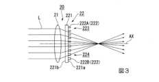
FIG. 3 is a side view of the
The
図3に示すように、光学装置20は、レンズ21と、位相変調素子22と、を備えている。レンズ21は、球面レンズで構成されている。位相変調素子22は、レンズ21の光射出側に設けられ、入射光Lの位相を変調することにより、レンズ21による収差を補正する。 As shown in FIG. 3, the
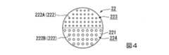
図4は、位相変調素子22の正面図である。図5は、位相変調素子22の側面図である。
図4に示すように、位相変調素子22は、基板221(基材)と、基板221の第1面221aに設けられた複数の柱状構造体222と、を備えている。図5に示すように、複数の柱状構造体222は、基板221の第1面221aの法線方向から見て、2次元状に周期的に並んで設けられている。複数の柱状構造体222は、基板221の第1面221aの全域に設けられている。柱状構造体222は、nmオーダーの径を有しており、ナノピラーなどと呼ばれることもある。FIG. 4 is a front view of the
As shown in FIG. 4, the
柱状構造体222は、例えば酸化チタン(TiO2)、窒化シリコン(SiN)、リン化ガリウム(GaP)等の高屈折率の誘電体材料から構成されている。柱状構造体222の形状は、例えば円柱状、正四角柱状等の回転対称形である。基板221は、柱状構造体222の屈折率よりも低い屈折率を有するガラス(SiO2)等の透光性基板から構成されている。レンズ21から射出され、位相変調素子22に入射する入射光Lは、基板221の第2面221bから入射され、第1面221aから射出される。なお、位相変調素子22は、図3とは逆に、入射光Lが基板221の第1面221aから入射され、第2面221bから射出される向きに配置されていてもよい。なお、柱状構造体222は、例えば金(Au)、銀(Ag)、銅(Cu)、白金(Pt)、パラジウム(Pd)、ニッケル(Ni)、アルミニウム(Al)等の金属材料から構成されていてもよい。The
複数の柱状構造体222は、入射光Lに対して導波路効果を生じさせる屈折率およびピッチを有している。柱状構造体222の屈折率は、2.2~4.0程度の範囲である。例えば柱状構造体222の材料であるTiO2の屈折率は2.28~2.42程度であり、SiNの屈折率は2.0~2.1程度であり、GaPの屈折率は3.1~4.0程度である。The multiple
柱状構造体222の太さ、すなわち、柱状構造体222の径Wは、例えば50~700nm程度である。隣り合う柱状構造体222間のピッチPは、例えば100~700nm程度である。なお、ピッチPは、隣り合う柱状構造体222の中心軸間の距離である。柱状構造体222の高さHは、例えば100~1000nm程度である。 The thickness of the
図4に示すように、基板221を入射光Lの射出方向から見たとき、基板221の形状は円形である。基板221の第1面221aは、第1光成分に対して位相を変調する複数の第1柱状構造体222Aが設けられた第1領域223と、第1光成分の特性パラメーターとは異なる特性パラメーターを有する第2光成分に対して位相を変調する複数の第2柱状構造体222Bが設けられた第2領域224と、を有する。本実施形態の場合、第1領域223および第2領域224のそれぞれは、基板221の外形をなす円を扇形状に分割した半円状の形状を有している。なお、基板221の形状は、必ずしも円形でなくてもよく、四角形を含む多角形等、他の形状であってもよい。
本明細書において、特性パラメーターは、位相変調素子22に入射する光の特性を示すパラメーターを意味し、具体的には、波長、入射角、偏光状態のいずれかに対応する。As shown in FIG. 4, when the
In this specification, a characteristic parameter means a parameter that indicates the characteristic of light incident on the
本実施形態では、第1光成分と第2光成分とは、光の特性パラメーターとしての波長が互いに異なっている。言い換えると、基板221の第1面221aは。第1領域223と第2領域224とに分割され、第1の波長に対して最適化された複数の第1柱状構造体222Aが第1領域223に設けられ、第1の波長とは異なる第2の波長に対して最適化された複数の第2柱状構造体222Bが第2領域224に設けられている。 In this embodiment, the first light component and the second light component have different wavelengths as light characteristic parameters. In other words, the
第1の波長を有する第1光成分と第2の波長を有する第2光成分との各々に対して最適化するため、第1柱状構造体222Aと第2柱状構造体222Bとは、柱状構造体222の径、ピッチ、高さ、および形状のうちの少なくとも一つの構造パラメーターが互いに異なっている。
本明細書において、構造パラメーターは、柱状構造体222の構造に関するパラメーターを意味し、具体的には、柱状構造体222の径、ピッチ、高さ、および形状のいずれかに対応する。In order to optimize for each of the first light component having the first wavelength and the second light component having the second wavelength, the first
In this specification, the structural parameter means a parameter related to the structure of the
位相変調素子22は、柱状構造体222の形成領域R内での光閉じ込め効果によって、ナノオーダーサイズの光共振器として作用する。また、後述するように、位相変調素子22は、例えば径W1,W2が異なる柱状構造体222A,222Bを有することにより、位相変調素子22を通過する光の位相を変調することができ、他の光学素子による収差を補正することができる。 The
位相変調は、柱状構造体222の形成領域R内での導波路効果(Waveguide effect)によって得られる。入射光Lの波長をλとし、柱状構造体222の実効屈折率をneffとし、柱状構造体222の高さをHとすると、位相変調量φは、以下の(1)式で表される。
φ=2π/λ×(neff×H) …(1)Phase modulation is obtained by a waveguide effect within the formation region R of the
φ=2π/λ×(neff×H) (1)
ここで、位相変調素子22における光の導波モードについて説明する。
光が柱状構造体222の形成領域に入射した際、以下の2つの導波モードによる光の導波が生じる。Here, the waveguide mode of light in the
When light is incident on the region where the
図7は、縦方向導波モードの概念を示す模式図である。図8は、横方向導波モードの概念を示す模式図である。
図7に示すように、位相変調素子22に対して垂直入射した光Lは、柱状構造体222の形成領域Rとその外側空間との界面で垂直に反射されることにより、反射光L1は、柱状構造体222の形成領域R内で往復し、共振を生じつつ導波する。この導波モードを縦方向導波モードと称する。縦方向導波モードは、ファブリーペロー共振器と同じ原理により生じる導波モードである。FIG. 7 is a schematic diagram showing the concept of the longitudinal waveguide mode. FIG. 8 is a schematic diagram showing the concept of the transverse waveguide mode.
As shown in FIG. 7, the light L vertically incident on the
また、位相変調素子22に対して入射した光は、柱状構造体222のピッチPに応じて所定の角度だけ回折される。このとき、複数の柱状構造体222は、回折格子として作用する。特に回折角が90°となる条件では、図8に示すように、回折光L2は、入射光Lに対して垂直方向に導波する。この導波モードを横方向導波モードと称する。 Also, the light incident on the
位相変調素子22においては、縦方向導波モードによる光の伝播と横方向導波モードによる光の伝播とが空気中で重なり合い、位相変調素子22から射出される光の位相が決まる。 In the
ここで、(1)式における実効屈折率neffは、柱状構造体222の径Wに依存する。そのため、柱状構造体222内への光の閉じ込めについては、柱状構造体222の径Wが大きい程、基本モードによる閉じ込めが増加する。したがって、柱状構造体222の径Wを変化させることにより、導波モードが変化し、実効屈折率neffも変化する。その結果、柱状構造体222の高さが一定であっても、位相変調が可能となる。 Here, the effective refractive index n eff in equation (1) depends on the diameter W of the
ここで、本発明者は、柱状構造体222の径Wを変化させた場合の位相シフト量のシミュレーションをFDTD法によって行った。ここでは、柱状構造体222の径Wのみを変化させ、柱状構造体222のピッチおよび高さは一定とした。 Here, the inventor performed a simulation of the phase shift amount when changing the diameter W of the
図6に、シミュレーション結果のグラフを示す。グラフの横軸は、柱状構造体の径(nm)であり、グラフの縦軸は、位相シフト量(/2π)である。
図6に示すように、柱状構造体222の径Wを250nmから420nmまで変化させたとき、位相シフト量(/2π)を約0.05から1まで変化させることができた。すなわち、柱状構造体222の径Wを大きくすると、位相変調量を大きくできることが判った。このことから、入射光Lの照射領域内の位置によって柱状構造体222の径Wを変えれば、位相変調量を変化させることが可能となる。FIG. 6 shows a graph of simulation results. The horizontal axis of the graph is the diameter (nm) of the columnar structure, and the vertical axis of the graph is the phase shift amount (/2π).
As shown in FIG. 6, when the diameter W of the
また、本発明者は、単色光、すなわち、特定の波長を有する光に対して最適化設計された位相変調素子22について、光強度分布の波長依存性のシミュレーションを行った。ここでは、波長550nmの入射光に対して最適化設計された位相変調素子を用いた。 Further, the present inventor conducted a simulation of the wavelength dependence of the light intensity distribution of the
図9に、シミュレーション結果のグラフを示す。グラフの横軸は、レンズの焦点位置からの距離X(μm)であり、グラフの縦軸は、光強度(a.u.)である。
図9に示すように、波長550nmの入射光に対しては十分に大きな光強度が得られるが、入射光の波長が設計値である550nmから、525nmまたは575nmというように、設計波長からのずれが大きくなるに従って、光強度は設計光強度の半分以下に低下してしまう。すなわち、集光効率が入射光の波長のずれによって急激に低下するため、設計波長以外の波長を有する光成分に対しては所望の位相変調が行われないことが判った。このような位相変調素子では、単色表示のプロジェクターにしか利用することができない。FIG. 9 shows a graph of simulation results. The horizontal axis of the graph is the distance X (μm) from the focal position of the lens, and the vertical axis of the graph is the light intensity (au).
As shown in FIG. 9, a sufficiently high light intensity is obtained for incident light with a wavelength of 550 nm. increases, the light intensity drops to less than half of the design light intensity. In other words, it has been found that the light collection efficiency is abruptly lowered by the wavelength shift of the incident light, so that the desired phase modulation is not performed for the light components having wavelengths other than the design wavelength. Such a phase modulation element can be used only for a monochromatic display projector.
これに対して、本実施形態の位相変調素子22においては、1枚の基板221を第1領域223と第2領域224との2つの領域に分割し、2つの領域の各々に、互いに異なる波長の光成分に対して最適化された複数の柱状構造体222がそれぞれ設けられている。一般的に、単球面レンズで生じる収差は、他の複数のレンズを用いて位相変調を行うことで低減することができるが、この方式では光学系が大きくなる、という欠点がある。一方、本実施形態の光学装置20では、薄型の位相変調素子22をレンズ21の後段に挿入しているため、基板221の厚さ分だけのスペースを確保すればよく、投影画像の解像度が高く、小型の光学装置20を得ることができる。 On the other hand, in the
また、複数の波長に対応可能な位相変調素子の設計手法は、論文(“Achromatic Metalens over 60 nm Bandwidth in the Visible and Metalens with Reverse Chromatic Dispersion”,Nano Letters,2017,17,pp1819-1824)で提案されている。ところが、この手法では、多波長化と効率とがトレードオフの関係にあり、素子の設計が複雑で難易度が高く、集光効率が低いことが課題となっている。 In addition, a design method for a phase modulation element that can handle multiple wavelengths was proposed in a paper (“Achromatic Metalens over 60 nm Bandwidth in the Visible and Metalens with Reverse Chromatic Dispersion”, Nano Letters, 2017, 17, pp1819-1824). It is However, in this method, there is a trade-off relationship between multi-wavelength and efficiency, and the problem is that the device design is complicated and difficult, and the light collection efficiency is low.
一方、単波長用の位相変調素子は、集光効率が高く、設計手法もシンプルである。したがって、本実施形態の位相変調素子22において、互いに異なる構造パラメーターを有する柱状構造体222A,222Bを2つの領域223,224に分割して配置した場合、入射光Lの波長と設計波長とが一致しない領域が生じるデメリットがあるものの、複数の波長を有する入射光Lに対応可能な位相変調素子22を容易に実現できる、という効果が得られる。 On the other hand, the single-wavelength phase modulation element has a high light collection efficiency and a simple design method. Therefore, in the
これにより、入射光Lが互いに異なる波長を有する複数の光成分を含む場合であっても、球面収差、コマ収差、非点収差、像面湾曲、歪曲収差等の各種収差に起因する画質低下が少ないコンパクトな光学装置20を実現することができる。 As a result, even when the incident light L includes a plurality of light components having different wavelengths, image quality degradation due to various aberrations such as spherical aberration, coma, astigmatism, curvature of field, and distortion can be prevented. A less compact
なお、分割した領域223,224毎の設計波長と同じ分布を持つ波長フィルターを位相変調素子22の前段に配置してもよい。これにより、設計波長と異なる波長を有する入射光Lが特定の領域に入射した際に発生するノイズ光を低減させることができ、上記のデメリットを解消することができる。 A wavelength filter having the same distribution as the design wavelength for each of the divided
本実施形態の光学装置20においては、レンズ21と位相変調素子22とが別個の部材として構成されているため、位相変調素子22を製造しやすく、所望の補正性能を得やすい。 In the
また、本実施形態においては、柱状構造体222の形状が円柱状等の回転対称形であるため、位相変調素子22において、構造性複屈折の効果は発生せず、入射光Lの偏光状態に依存することなく、収差補正の効果が得られる。なお、柱状構造体222の形状は、必ずしも円柱状等の回転対称形でなくてもよい。 In addition, in the present embodiment, since the shape of the
本実施形態のプロジェクター1は、上記の光学装置20を用いたことによって、投影画像の解像度が高く、表示品位に優れるとともに、小型化が実現できる。 By using the
本実施形態のように、互いに異なる波長を有する光成分に対応した領域223,224を有する位相変調素子22をプロジェクター1に適用する場合、例えば蛍光体ホイール50の後段のピックアップ光学系60に用いることが好適である。ピックアップ光学系60において、蛍光体ホイール50から射出された励起光Bとランバート分布を有する蛍光YLとでは、発光強度分布が異なる。したがって、位相変調素子22の中心付近は青色光の波長用に設計し、位相変調素子22の周縁付近は黄色光の波長用に設計する。これにより、光量のロスが少なく、かつ均一な光強度分布が得られる光学系を実現することができる。 When the
[第2実施形態]
以下、本発明の第2実施形態について、図10を用いて説明する。
第2実施形態の光学装置の基本構成は第1実施形態と同様であり、位相変調素子の各領域内の柱状構造体の設計が第1実施形態と異なる。そのため、光学装置の全体構成の説明は省略する。[Second embodiment]
A second embodiment of the present invention will be described below with reference to FIG.
The basic configuration of the optical device of the second embodiment is the same as that of the first embodiment, and the design of the columnar structure in each region of the phase modulating element is different from that of the first embodiment. Therefore, description of the overall configuration of the optical device is omitted.
本実施形態においても、第1実施形態と同様、基板の第1面は、第1光成分に対して位相を変調する複数の第1柱状構造体が設けられた第1領域と、第2光成分に対して位相を変調する複数の第2柱状構造体が設けられた第2領域と、を有する。 Also in this embodiment, as in the first embodiment, the first surface of the substrate includes a first region provided with a plurality of first columnar structures that modulate the phase of the first light component, and a second light component. and a second region provided with a plurality of second columnar structures that modulate the phase of the component.
本実施形態では、第1光成分と第2光成分とは、光の特性パラメーターとしての入射角が互いに異なっている。言い換えると、基板の第1面は第1領域と第2領域とに分割され、第1の入射角に最適化された複数の第1柱状構造体が第1領域に設けられ、第1の入射角とは異なる第2の入射角に最適化された複数の第2柱状構造体が第2領域に設けられている。 In the present embodiment, the first light component and the second light component have different incident angles as light characteristic parameters. In other words, the first surface of the substrate is divided into a first area and a second area, a plurality of first columnar structures optimized for a first incident angle are provided in the first area, and the first incident angle A plurality of second columnar structures optimized for a second angle of incidence different from the angle are provided in the second region.
第1の入射角を有する第1光成分と第2の入射角を有する第2光成分との各々に対して最適化するため、第1柱状構造体と第2柱状構造体とは、柱状構造体の径、ピッチ、高さ、および形状のうちの少なくとも一つの構造パラメーターが互いに異なっている。 In order to optimize for each of the first light component with the first angle of incidence and the second light component with the second angle of incidence, the first columnar structure and the second columnar structure are composed of columnar structures At least one structural parameter of body diameter, pitch, height and shape is different from each other.
本発明者は、特定の波長を有する光に対して最適化設計された位相変調素子について、光強度分布の入射角依存性のシミュレーションを行った。ここでは、入射角が0°の入射光に対して最適化設計された位相変調素子を用いた。 The present inventor conducted a simulation of the incident angle dependence of the light intensity distribution for a phase modulation element optimized for light having a specific wavelength. Here, a phase modulation element optimized for incident light with an incident angle of 0° was used.
図10に、シミュレーション結果のグラフを示す。グラフの横軸は、レンズの焦点位置からの距離X(μm)であり、グラフの縦軸は、光強度(a.u.)である。
図10に示すように、入射角が0°の入射光に対しては十分に大きな光強度が得られるが、設計入射角である0°から2°、4°、6°というように、設計入射角からのずれが大きくなるに従って、光強度は急激に低下する。すなわち、集光効率は入射角のずれによって急激に低下するため、設計入射角以外の入射角を有する光成分については所望の位相変調が行われないことが判った。したがって、広い入射角範囲を持つ光が入射する可能性がある光学系やズームレンズには、この位相変調素子を用いることが難しい。FIG. 10 shows a graph of simulation results. The horizontal axis of the graph is the distance X (μm) from the focal position of the lens, and the vertical axis of the graph is the light intensity (au).
As shown in FIG. 10, a sufficiently high light intensity can be obtained for incident light with an incident angle of 0°. The light intensity drops sharply as the deviation from the incident angle increases. In other words, it has been found that the light collection efficiency is abruptly lowered by the deviation of the incident angle, so that the desired phase modulation is not performed for the light component having the incident angle other than the designed incident angle. Therefore, it is difficult to use this phase modulation element in an optical system or a zoom lens that may receive light with a wide range of incident angles.
これに対し、本実施形態の位相変調素子においては、基板上の2つの領域の各々に、互いに異なる入射角の光成分に対して最適化された複数の柱状構造体がそれぞれ設けられている。これにより、複数の入射角を有する光に対応可能な位相変調素子を容易に実現することができる。 On the other hand, in the phase modulation element of this embodiment, each of the two regions on the substrate is provided with a plurality of columnar structures optimized for light components with different incident angles. This makes it possible to easily realize a phase modulation element that can handle light having a plurality of incident angles.
[第3実施形態]
以下、本発明の第3実施形態について説明する。
第3実施形態の光学装置の基本構成は第1実施形態と同様であり、位相変調素子の各領域内の柱状構造体の設計が第1実施形態と異なる。そのため、光学装置の全体構成の説明は省略する。[Third embodiment]
A third embodiment of the present invention will be described below.
The basic configuration of the optical device of the third embodiment is the same as that of the first embodiment, and the design of the columnar structure in each region of the phase modulation element is different from that of the first embodiment. Therefore, description of the overall configuration of the optical device is omitted.
本実施形態においても、第1実施形態と同様、基板の第1面は、第1光成分に対して位相を変調する複数の第1柱状構造体が設けられた第1領域と、第2光成分に対して位相を変調する複数の第2柱状構造体が設けられた第2領域と、を有する。 Also in this embodiment, as in the first embodiment, the first surface of the substrate includes a first region provided with a plurality of first columnar structures that modulate the phase of the first light component, and a second light component. and a second region provided with a plurality of second columnar structures that modulate the phase of the component.
本実施形態では、第1光成分と第2光成分とは、入射光の特性パラメーターとしての偏光状態が互いに異なっている。言い換えると、基板の第1面は第1領域と第2領域に分割され、第1の偏光状態を有する入射光に最適化された複数の第1柱状構造体が第1領域に設けられ、第1の偏光状態とは異なる第2の偏光状態を有する入射光に最適化された複数の第2柱状構造体が第2領域に設けられている。 In this embodiment, the first light component and the second light component have different polarization states as characteristic parameters of the incident light. In other words, the first surface of the substrate is divided into a first region and a second region, a plurality of first columnar structures optimized for incident light having a first polarization state are provided in the first region, A plurality of second columnar structures optimized for incident light having a second polarization state different from the one polarization state are provided in the second region.
第1の偏光状態を有する第1光成分と第2の偏光状態を有する第2光成分との各々に対して最適化するため、第1柱状構造体と第2柱状構造体とは、柱状構造体の径、ピッチ、高さ、および形状のうちの少なくとも一つの構造パラメーターが互いに異なっている。 In order to optimize for each of the first light component with the first polarization state and the second light component with the second polarization state, the first columnar structure and the second columnar structure are composed of columnar structures At least one structural parameter of body diameter, pitch, height and shape is different from each other.
第1実施形態のように、柱状構造体の形状が円柱状などの回転対称形である場合、位相変調特性が入射光の偏光状態に依存しないが、柱状構造体の設計の自由度が制限される、一方、柱状構造体の形状が回転対称形でない場合、柱状構造体の設計パラメーターが多くなるために設計自由度が増す反面、位相変調特性が入射光の偏光状態に依存する。 As in the first embodiment, when the shape of the columnar structure is rotationally symmetrical, such as a cylindrical shape, the phase modulation characteristic does not depend on the polarization state of the incident light, but the degree of freedom in designing the columnar structure is limited. On the other hand, if the shape of the columnar structure is not rotationally symmetrical, the number of design parameters of the columnar structure increases and the degree of freedom in design increases, but the phase modulation characteristic depends on the polarization state of incident light.
これに対し、本実施形態の位相変調素子においては、基板上の2つの領域の各々に、互いに異なる偏光状態を有する光成分に対して最適化された複数の柱状構造体がそれぞれ設けられている。これにより、複数の偏光状態を有する光に対応可能な位相変調素子を容易に実現することができる。 On the other hand, in the phase modulation element of this embodiment, each of the two regions on the substrate is provided with a plurality of columnar structures optimized for light components having different polarization states. . This makes it possible to easily realize a phase modulation element that can handle light having a plurality of polarization states.
なお、分割した領域の偏光状態と同じ偏光分布を持つ偏光フィルターを位相変調素子の前段に配置してもよい。これにより、設計偏光と異なる偏光状態を有する入射光が特定の領域に入射することで発生するノイズ光を低減させることができる。 A polarizing filter having the same polarization distribution as the polarization state of the divided regions may be arranged in front of the phase modulation element. As a result, it is possible to reduce noise light generated when incident light having a polarization state different from the design polarization enters a specific region.
[柱状構造体の構造パラメーターについて]
上述したように、波長、入射角、および偏光状態の入射光の特性パラメーターのいずれに対して各領域を最適化する場合であっても、柱状構造体の径、ピッチ、高さ、形状の構造パラメーターのいずれを領域毎に異ならせてもよい。ただし、以下に示すように、各特性パラメーターに対して最も与える影響が大きい柱状構造体の構造パラメーターが存在する。[Regarding Structural Parameters of Columnar Structures]
As noted above, the structure of the diameter, pitch, height and shape of the pillars, whether optimizing each region for the characteristic parameters of wavelength, angle of incidence and polarization state of the incident light. Any of the parameters may vary from region to region. However, as shown below, there is a structural parameter of the columnar structure that exerts the greatest influence on each characteristic parameter.
具体的には、第1実施形態のように、領域毎に設計波長を異ならせる場合、柱状構造体のピッチが与える影響が最も大きい。第2実施形態のように、領域毎に設計入射角を異ならせる場合、柱状構造体の径が与える影響が最も大きい。第3実施形態のように、領域毎に設計偏光状態を異ならせる場合、柱状構造体の断面形状が与える影響が最も大きい。ただし、入射光の各特性パラメーターを異ならせる場合、必ずしも上述した構造パラメーターのみを異ならせるとは限らない。最も影響が大きい構造パラメーターに加え、別の構造パラメーターを同時に異ならせることも考えられる。上記では、あくまでも最も影響が大きい構造パラメーターを示した。 Specifically, when the design wavelength is different for each region as in the first embodiment, the pitch of the columnar structure has the greatest effect. As in the second embodiment, when the designed incident angle is different for each region, the diameter of the columnar structure has the greatest effect. When the designed polarization state is different for each region as in the third embodiment, the cross-sectional shape of the columnar structure has the greatest influence. However, when each characteristic parameter of incident light is made different, it is not necessarily the case that only the structural parameter mentioned above is made different. In addition to the most influential structural parameter, it is also conceivable to vary other structural parameters at the same time. The above only shows the structural parameters that have the greatest impact.
(設計波長について)
位相変調素子の柱状構造体のピッチPは、位相変調素子がレンズとして機能するための条件として、下記の(1)式で表されるナイキストの標本化定理から導かれる関係式を満たす必要がある。
P<λ/N.A. …(1)
λ:波長、N.A.:レンズの開口数(About design wavelength)
The pitch P of the columnar structures of the phase modulating element must satisfy the relational expression derived from the Nyquist sampling theorem represented by the following formula (1) as a condition for the phase modulating element to function as a lens. .
P<λ/NA (1)
λ: wavelength, NA: lens numerical aperture
よって、波長によって柱状構造体のピッチPの最大値が異なる。また、導波モード共鳴を利用した位相変調素子の場合は、共鳴波長は柱状構造体のピッチPに依存するため、位相変調素子の設計波長によって柱状構造体のピッチPは変化する。 Therefore, the maximum value of the pitch P of the columnar structure differs depending on the wavelength. Further, in the case of a phase modulation element using waveguide mode resonance, the resonance wavelength depends on the pitch P of the columnar structures, so the pitch P of the columnar structures changes depending on the design wavelength of the phase modulation element.
(設計入射角について)
図11は、入射光Lが位相変調素子22に垂直入射した場合の等位相面Tを示す図である。図12は、入射光Lが位相変調素子22に斜め入射した場合の等位相面Tを示す図である。
図11に示すように、位相変調素子22に対して平面波からなる入射光Lを垂直入射させた場合、柱状構造体222に対して全て同位相の波が入射する。一方、図12に示すように、位相変調素子22に対して平面波からなる入射光Lを斜め入射させた場合、柱状構造体222に入射する光波の位相は柱状構造体222ごとに異なる。(Regarding the design incident angle)
FIG. 11 is a diagram showing the equiphase plane T when the incident light L is vertically incident on the
As shown in FIG. 11 , when incident light L composed of plane waves is vertically incident on the
そのため、位相変調素子22に、レンズ機能を得るための位相差と、斜め入射による位相差を補正するための位相差と、の双方を発生させる必要がある。その結果、隣り合う柱状構造体222で発生する位相差の変化量は、入射光Lが斜め入射した場合の方が、入射光Lが垂直入射した場合よりも大きくなる。柱状構造体222で発生させる位相差は、柱状構造体222の径で調整できるため、隣接する柱状構造体の径の変化量は設計入射角に応じて異なる。 Therefore, it is necessary to generate both a phase difference for obtaining a lens function and a phase difference for correcting the phase difference due to oblique incidence in the
(設計偏光について)
柱状構造体の形状が円柱などの回転対称形である場合、入射偏光状態に依存することなく、所望の位相差を発生させることが可能である。一方、柱状構造体の形状が、例えば断面が長方形の四角柱などの非回転対称形である場合、入射光の振動方向によって波面の遅延が非対称に生じるため、発生する位相差は偏光状態の影響を大きく受ける。(About design polarization)
When the shape of the columnar structure is rotationally symmetrical, such as a cylinder, it is possible to generate a desired phase difference without depending on the incident polarization state. On the other hand, if the shape of the columnar structure is a non-rotationally symmetrical shape such as a square column with a rectangular cross section, the wavefront delay occurs asymmetrically depending on the vibration direction of the incident light, so the generated phase difference is affected by the polarization state. greatly received.
したがって、特定の偏光状態の光に対してのみ、所望の位相差を発生させる位相変調素子を設計する場合には、柱状構造体の形状が非回転対称形となるため、設計偏光方向によって柱状構造体の断面形状が互いに異なる。 Therefore, when designing a phase modulation element that generates a desired phase difference only for light in a specific polarization state, the shape of the columnar structure is rotationally asymmetric. The cross-sectional shapes of the bodies are different from each other.
[第4実施形態]
以下、本発明の第4実施形態について、図13を用いて説明する。
第4実施形態の光学装置の基本構成は第1実施形態と同様であり、位相変調素子の構成が第1実施形態と異なる。そのため、光学装置の全体構成の説明は省略する。
図13は、第4実施形態の光学装置の側面図である。
図13において、第1実施形態で用いた図3と共通の構成要素には同一の符号を付し、説明を省略する。[Fourth embodiment]
A fourth embodiment of the present invention will be described below with reference to FIG.
The basic configuration of the optical device of the fourth embodiment is the same as that of the first embodiment, and the configuration of the phase modulating element is different from that of the first embodiment. Therefore, description of the overall configuration of the optical device is omitted.
FIG. 13 is a side view of the optical device of the fourth embodiment.
In FIG. 13, the same reference numerals are given to the same constituent elements as in FIG. 3 used in the first embodiment, and the description thereof is omitted.
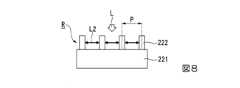
第1~第3実施形態の光学装置においては、透過型の位相変調素子が用いられていたのに対し、第4実施形態の光学装置36においては、反射型の位相変調素子37が用いられている。したがって、本実施形態の光学装置36は、図1に示すプロジェクター1において、例えば第1反射ミラー8a、第2反射ミラー8b、第3反射ミラー8c等の反射素子が用いられる個所に適用することができる。 In contrast to the transmission type phase modulation element used in the optical devices of the first to third embodiments, the reflection type
図14に示すように、本実施形態の光学装置36は、レンズ21と、位相変調素子37と、を備えている。位相変調素子37は、基材38と、基材38に設けられた複数の柱状構造体222と、を有する。基材38は、第1面381aと第2面381bとを有するスペーサー層381と、スペーサー層381の第2面381bに設けられた反射層382と、を有する。 As shown in FIG. 14, the
スペーサー層381の構成材料として、例えばSiO2等が用いられる。スペーサー層381は、柱状構造体222の屈折率よりも低い屈折率を有する。スペーサー層381の屈折率は、例えば1.3~2.1程度である。第1実施形態で述べたように、柱状構造体222の屈折率は2.2~4.0程度であるため、柱状構造体222の屈折率とスペーサー層381の屈折率との差は、0.1以上であることが望ましい。また、反射層382の構成材料として、高反射率を有する金属膜、もしくは誘電体多層膜が用いられる。As a constituent material of the
本実施形態の位相変調素子37は反射型の位相変調素子であるため、レンズ21から射出された光は、スペーサー層381の第1面381aから入射された後、反射層382で反射され、スペーサー層381の第1面381aから後段の光学系に向けて射出される。 Since the
光学装置36のその他の構成は、第1実施形態と同様である。すなわち、基材38の第1面は、第1光成分に対して位相を変調する複数の第1柱状構造体222Aが設けられた第1領域223と、第1光成分の特性パラメーターとは異なる特性パラメーターを有する第2光成分に対して位相を変調する複数の第2柱状構造体222Bが設けられた第2領域224と、を有する。第1光成分と第2光成分とは、光の特性パラメーターとしての波長が互いに異なっている。なお、第1光成分と第2光成分とは、光の特性パラメーターとして、第2実施形態のように入射角が互いに異なっていてもよいし、第3実施形態のように偏光状態が互いに異なっていてもよい。 Other configurations of the
本実施形態においても、複数の波長、複数の入射角、および複数の偏光状態等、複数の特性パラメーターを有する光に対応可能な位相変調素子37を容易に実現することができる、といった第1~第3実施形態と同様の効果が得られる。 Also in the present embodiment, the first to that the
また、本実施形態においては、位相変調素子37と反射ミラーとが一体化されているため、各種の収差による画質低下が少ないコンパクトな光学装置36を実現することができる。 Further, in this embodiment, since the
[複数の領域の配置に関する変形例]
第1~第4実施形態の位相変調素子において、上記の第1領域および第2領域に加えて、より多くの領域が設けられていてもよい。また、それらの領域は、以下に示すように配置されていてもよい。[Modified Example of Arrangement of Multiple Areas]
In addition to the above-described first and second regions, more regions may be provided in the phase modulation elements of the first to fourth embodiments. Also, these regions may be arranged as shown below.
図14は、第1変形例の位相変調素子71の正面図である。
図14に示すように、第1変形例の位相変調素子71において、基板221の第1面は、第1光成分に対して位相を変調する複数の第1柱状構造体(図示略)が設けられた第1領域711と、第1光成分の特性パラメーターとは異なる特性パラメーターを有する第2光成分に対して位相を変調する複数の第2柱状構造体(図示略)が設けられた第2領域712と、第1光成分および第2光成分の特性パラメーターとは異なる特性パラメーターを有する第3光成分に対して位相を変調する複数の第3柱状構造体(図示略)が設けられた第3領域713と、第1光成分、第2光成分、および第3光成分の特性パラメーターとは異なる特性パラメーターを有する第4光成分に対して位相を変調する複数の第4柱状構造体(図示略)が設けられた第4領域714と、を有する。FIG. 14 is a front view of the
As shown in FIG. 14, in the
本変形例の場合、第1領域711、第2領域712、第3領域713、および第4領域714は、基板221の中心に対して同心円状に配置されている。 In this modification, the
本変形例においても、複数の波長、複数の入射角、および複数の偏光状態等、複数の特性パラメーターを有する光に対応可能な位相変調素子71を容易に実現することができる、といった第1~第4実施形態と同様の効果が得られる。 In this modified example as well, the first to that the
また、本変形例の場合、第1領域711、第2領域712、第3領域713、および第4領域714が同心円状に配置されているため、入射光の入射位置が設計上の位置からずれた場合でも、複数の領域711,712,713,714のどこかに入射させることが可能となる。 In addition, in the case of this modification, since the
図15は、第2変形例の位相変調素子72の正面図である。
図15に示すように、第2変形例の位相変調素子72においても、第1変形例と同様、基板221の第1面は、第1領域721と、第2領域722と、第3領域723と、第4領域724と、を有する。FIG. 15 is a front view of the
As shown in FIG. 15, in the
本変形例の場合、第1領域721、第2領域722、第3領域723、および第4領域724は、基板221の中心に対して格子状に配置されている。基板221が格子状に分割された矩形状の各領域に対して、第1領域721、第2領域722、第3領域723、および第4領域724をどのように配置するかは任意である。例えば4つの領域の配置が規則性を有しておらず、第1領域721、第2領域722、第3領域723、および第4領域724がランダムに配置されていてもよい。 In the case of this modification, the
本変形例においても、複数の波長、複数の入射角、および複数の偏光状態等、複数の特性パラメーターを有する光に対応可能な位相変調素子72を容易に実現することができる、といった第1~第4実施形態と同様の効果が得られる。 Also in this modification, the first to that the
特に第1領域721、第2領域722、第3領域723、および第4領域724がランダムに配置された場合、入射光の入射位置が設計位置からずれた場合でも、特定の特性パラメーターに対応した領域に入射光の強度が偏って分布することが抑えられる。 In particular, when the
図16は、第3変形例の位相変調素子73の正面図である。
図16に示すように、第3変形例の位相変調素子73においても、第1変形例と同様、基板221の第1面は、第1領域731と、第2領域732と、第3領域733と、第4領域734と、を有する。FIG. 16 is a front view of the
As shown in FIG. 16, in the
本変形例の場合、第1領域731、第2領域732、第3領域733、および第4領域734は、基板221の中心に対して扇形状に配置されている。第1領域731、第2領域732、第3領域733、および第4領域734は、基板221の周方向にこの順に配置されていてもよいし、ランダムな順番で配置されていてもよい。 In the case of this modification, the
本変形例においても、複数の波長、複数の入射角、および複数の偏光状態等、複数の特性パラメーターを有する光に対応可能な位相変調素子73を容易に実現することができる、といった第1~第4実施形態と同様の効果が得られる。 Also in this modified example, the first to that the
特に本変形例において、基板221の中心に光を入射させた場合、光強度が強い基板221の中心に全ての領域731,732,733,734が集まって配置されているため、複数の波長、入射角、および偏光状態に対する位相変調を確実に行うことができる。 Especially in this modified example, when light is incident on the center of the
図17は、第4変形例の位相変調素子74の正面図である。
図17に示すように、第4変形例の位相変調素子74においても、第1変形例と同様、基板221の第1面は、第1領域741と、第2領域742と、第3領域743と、第4領域744と、を有する。FIG. 17 is a front view of the
As shown in FIG. 17, in the
本変形例の場合、第1領域741、第2領域742、第3領域743、および第4領域744は、基板221上に不定形状をもって配置されている。各領域741,742,743,744の面積は、図17に示すように、適宜異ならせてもよいし、同じにしてもよい。 In the case of this modification, the
本変形例においても、複数の波長、複数の入射角、および複数の偏光状態等、複数の特性パラメーターを有する光に対応可能な位相変調素子74を容易に実現することができる、といった第1~第4実施形態と同様の効果が得られる。 In this modified example as well, the first to that the
特に本変形例の場合、入射光の面内の光強度分布が不均一な場合に、特定仕様の領域741,742,743,744の面積を増加させて光利用効率を向上させたり、領域741,742,743,744の面積を調整することで特定の特性パラメーターを有する光成分の強度を調整したりすることができる。 Especially in the case of this modification, when the light intensity distribution in the plane of the incident light is uneven, the areas of the
なお、本発明の技術範囲は上記実施形態に限定されるものではなく、本発明の趣旨を逸脱しない範囲において種々の変更を加えることが可能である。
例えば上記実施形態では、位相変調素子の各領域が光の波長、入射角、および偏光状態のうちのいずれか一つの特性パラメーターに対応した例を挙げたが、位相変調素子の各領域が2つ以上の特性パラメーターに対応していてもよい。また、位相変調素子がレンズ機能を有してもよく、その場合には必ずしもレンズと組み合わせて用いなくてもよい。The technical scope of the present invention is not limited to the above embodiments, and various modifications can be made without departing from the scope of the present invention.
For example, in the above embodiments, each region of the phase modulation element corresponds to any one of the wavelength, incident angle, and polarization state of light. It may correspond to the above characteristic parameters. Also, the phase modulation element may have a lens function, and in that case, it does not necessarily have to be used in combination with a lens.
また、上記実施形態では、柱状構造体が円柱状、正四角柱状等の場合を例示したが、底面の面積が上面の面積よりも広いテーパー形状を有していてもよい。この構成によれば、例えばレンズの曲面上に柱状構造体を形成しても、隣り合う柱状構造体の側面同士の平行度を維持することができる。例えばテーパー面の傾斜角度は法線方向に対して15°以下程度でよい。また、ナノオーダーの柱状構造体を形成する手段の一つとして、ナノインプリント法が挙げられる。ナノインプリント法を用いて柱状構造体を形成する場合、柱状構造体がテーパー形状を有していれば、柱状構造体材料から転写型を剥離する際の剥離作業を容易に行うことができ、所望の形状を有する柱状構造体を得やすい。 Further, in the above-described embodiments, the columnar structure has a columnar shape, a square columnar shape, or the like, but it may have a tapered shape in which the area of the bottom surface is larger than the area of the top surface. With this configuration, for example, even if the columnar structures are formed on the curved surface of the lens, the parallelism between the side surfaces of the adjacent columnar structures can be maintained. For example, the inclination angle of the tapered surface may be approximately 15° or less with respect to the normal direction. Further, as one of means for forming a nano-order columnar structure, there is a nanoimprint method. When a columnar structure is formed using a nanoimprinting method, if the columnar structure has a tapered shape, it is possible to easily perform a peeling operation when the transfer mold is peeled off from the columnar structure material. It is easy to obtain a columnar structure having a shape.
また、位相変調素子を構成する各構成要素の形状、数、配置、材料等の具体的な構成については、上記実施形態に限定されることなく、適宜変更が可能である。また、上記実施形態では、照明装置が、青色の励起光を射出する光源と蛍光体ホイールとを備え、蛍光体ホイール上の蛍光体層に励起光を照射して蛍光を得る方式の照明装置に本発明を適用したが、青色光を射出するレーザー光源、緑色光を射出するレーザー光源、および赤色光を射出するレーザー光源を備え、これらのレーザー光源からの各色光を用いて直接画像を表示するプロジェクターに本発明を適用してもよい。 Further, the specific configuration such as the shape, number, arrangement, and material of each component constituting the phase modulating element is not limited to the above embodiment, and can be changed as appropriate. Further, in the above-described embodiment, the lighting device includes a light source that emits blue excitation light and a phosphor wheel, and the lighting device obtains fluorescence by irradiating the phosphor layer on the phosphor wheel with the excitation light. Although the present invention is applied, it has a laser light source that emits blue light, a laser light source that emits green light, and a laser light source that emits red light, and directly displays an image using each color light from these laser light sources. The present invention may be applied to projectors.
また、上記実施形態の位相変調素子は、図1に示したプロジェクターの光学系に限らず、スキャナー装置、インタラクティブプロジェクター用のセンシング用赤外波長投射光学装置、カメラなどの撮像装置等にも適用が可能である。また、光学装置は、プロジェクターに限らず、ヘッドマウントディスプレイ等の表示装置にも適用が可能である。 In addition, the phase modulation element of the above embodiment is not limited to the optical system of the projector shown in FIG. It is possible. Further, the optical device is applicable not only to projectors but also to display devices such as head-mounted displays.
1…プロジェクター(表示装置)、22,37,71,72,73,74…位相変調素子、38…基材、221…基板(基材)、221a…第1面、222…柱状構造体、222A…第1柱状構造体、222B…第2柱状構造体、223,711,721,731,741…第1領域、224,712,722,732,742…第2領域、381…スペーサー層、382…反射層、L…入射光。 DESCRIPTION OF
Claims (5)
Translated fromJapanese前記基材の第1面に設けられた複数の柱状構造体と、
を備え、
前記複数の柱状構造体は、第1光成分と、前記第1光成分とは波長、入射角、および偏光状態のうちの少なくとも一つの異なる特性パラメーターを有する第2光成分と、を含む入射光に対して導波路効果を生じさせる屈折率およびピッチを有し、
前記基材の前記第1面は、前記第1光成分に対して位相を変調する複数の第1柱状構造体が設けられた第1領域と、前記第2光成分に対して位相を変調する複数の第2柱状構造体が設けられた第2領域と、を有し、
前記基材は、第1面と第2面とを有するスペーサー層と、反射層と、を有し、
前記複数の柱状構造体は、前記スペーサー層の第1面に設けられ、
前記反射層は、前記スペーサー層の第2面に設けられ、
前記スペーサー層の屈折率は、前記柱状構造体の屈折率よりも低く、
前記入射光は、前記スペーサー層の前記第1面から入射され、前記反射層で反射され、前記スペーサー層の前記第1面から射出される位相変調素子。a substrate;
a plurality of columnar structures provided on the first surface of the base;
with
The plurality of columnar structures are incident including a first light component and a second lightcomponent havingat least one characteristic parameter different from the first light component in terms of wavelength, incident angle, and polarization state. having a refractive index and pitch that produce a waveguide effect for light,
The first surface of the substrate includes a first region provided with a plurality of first columnar structures that modulate the phase of the first light component, and a first region that modulates the phase of the second light component. a second region provided with a plurality of second columnar structures;
The substrate has a spacer layer having a first surface and a second surface, and a reflective layer,
The plurality of columnar structures are provided on the first surface of the spacer layer,
the reflective layer is provided on the second surface of the spacer layer;
The spacer layer has a lower refractive index than the columnar structures,
The incident light is incident from the first surface of the spacer layer, reflected by the reflective layer, and emitted from the first surface of the spacer layer.
前記第1領域と前記第2領域とは、同心円状、格子状、扇形状、および不定形状のうちのいずれかの形態で配置されている、請求項1または請求項2に記載の位相変調素子。When the base material is viewed from the direction in which the incident light is emitted, the shape of the base material is circular,
3. The phase modulating element according to claim 1, wherein said first region andsaid second region are arranged in any one of concentric circles, lattice, sector, and irregular shapes. .
前記複数の柱状構造体は、前記透光性基板の第1面に設けられ、
前記入射光は、前記透光性基板の前記第1面および前記第2面のうちのいずれか一方から入射され、前記第1面および前記第2面のうちのいずれか他方から射出される、請求項1から請求項3までのいずれか一項に記載の位相変調素子。The base material has a translucent substrate having a first surface and a second surface,
The plurality of columnar structures are provided on the first surface of the translucent substrate,
the incident light is incident from either one of the first surface and the second surface of the translucent substrate, and is emitted from the other of the first surface and the second surface; The phase modulating element according to any one of claims 1 to3 .
Priority Applications (3)
| Application Number | Priority Date | Filing Date | Title |
|---|---|---|---|
| JP2019178866AJP7334564B2 (en) | 2019-09-30 | 2019-09-30 | Phase modulation element and display device |
| CN202011039652.8ACN112578492B (en) | 2019-09-30 | 2020-09-28 | Phase modulation element and display device |
| US17/037,204US11317066B2 (en) | 2019-09-30 | 2020-09-29 | Phase modulation element and display device |
Applications Claiming Priority (1)
| Application Number | Priority Date | Filing Date | Title |
|---|---|---|---|
| JP2019178866AJP7334564B2 (en) | 2019-09-30 | 2019-09-30 | Phase modulation element and display device |
Publications (2)
| Publication Number | Publication Date |
|---|---|
| JP2021056370A JP2021056370A (en) | 2021-04-08 |
| JP7334564B2true JP7334564B2 (en) | 2023-08-29 |
Family
ID=75119690
Family Applications (1)
| Application Number | Title | Priority Date | Filing Date |
|---|---|---|---|
| JP2019178866AActiveJP7334564B2 (en) | 2019-09-30 | 2019-09-30 | Phase modulation element and display device |
Country Status (3)
| Country | Link |
|---|---|
| US (1) | US11317066B2 (en) |
| JP (1) | JP7334564B2 (en) |
| CN (1) | CN112578492B (en) |
Families Citing this family (5)
| Publication number | Priority date | Publication date | Assignee | Title |
|---|---|---|---|---|
| CN115265401A (en)* | 2021-04-29 | 2022-11-01 | 华为技术有限公司 | Camera module and electronic equipment |
| JP7732352B2 (en)* | 2021-12-22 | 2025-09-02 | セイコーエプソン株式会社 | projector |
| JPWO2023188947A1 (en)* | 2022-03-31 | 2023-10-05 | ||
| CN118805101A (en)* | 2022-03-31 | 2024-10-18 | 松下知识产权经营株式会社 | Optical lens |
| TWI831413B (en)* | 2022-10-12 | 2024-02-01 | 大陸商廣州立景創新科技有限公司 | Metalens and image sensor |
Citations (7)
| Publication number | Priority date | Publication date | Assignee | Title |
|---|---|---|---|---|
| JP2007057622A (en) | 2005-08-22 | 2007-03-08 | Ricoh Co Ltd | Optical element and manufacturing method thereof, manufacturing method of shape transfer mold for optical element, and transfer mold for optical element |
| JP2016029883A (en) | 2014-07-16 | 2016-03-03 | タレス | Photovoltaic module including concentration optic with subwavelength patterns, and solar power generator for satellite including the same module |
| JP2018097142A (en) | 2016-12-13 | 2018-06-21 | リコーインダストリアルソリューションズ株式会社 | Speckle dissolution optical system |
| JP2018537804A (en) | 2015-09-23 | 2018-12-20 | オスラム・シルバニア・インコーポレイテッド | Collimating / Metal lens and technology incorporating it |
| JP2019028450A (en) | 2017-07-31 | 2019-02-21 | 三星電子株式会社Samsung Electronics Co.,Ltd. | Meta-projector and electronic device including the same |
| JP2019086765A (en) | 2017-11-08 | 2019-06-06 | 三星電子株式会社Samsung Electronics Co.,Ltd. | Projector including metal lens |
| JP2019516128A (en) | 2016-04-05 | 2019-06-13 | プレジデント・アンド・フェロウズ・オブ・ハーバード・カレッジ | Metalens for sub-wavelength resolution imaging |
Family Cites Families (7)
| Publication number | Priority date | Publication date | Assignee | Title |
|---|---|---|---|---|
| JP2001066499A (en) | 1999-08-26 | 2001-03-16 | Canon Inc | Optical system having diffractive optical element |
| CN101535177B (en)* | 2006-11-10 | 2012-06-13 | 住友电气工业株式会社 | Si-o containing hydrogenated carbon film, optical device including the same, and method for manufacturing the si-o containing hydrogenated film and the optical device |
| JP2009175238A (en)* | 2008-01-22 | 2009-08-06 | Seiko Epson Corp | Optical element and light source unit |
| WO2014189507A1 (en)* | 2013-05-22 | 2014-11-27 | Hewlett-Packard Development Company, L.P. | Optical devices including a high contrast grating lens |
| CN105700163A (en)* | 2016-04-07 | 2016-06-22 | 武汉华星光电技术有限公司 | Cylindrical lens film and 3D display device |
| JP2017198845A (en) | 2016-04-27 | 2017-11-02 | 京セラ株式会社 | Reflection angle controllable transparent material |
| KR102692564B1 (en)* | 2018-09-21 | 2024-08-06 | 삼성전자주식회사 | Multi-layer structure and phase shift device using the multi-layer structure |
- 2019
- 2019-09-30JPJP2019178866Apatent/JP7334564B2/enactiveActive
- 2020
- 2020-09-28CNCN202011039652.8Apatent/CN112578492B/enactiveActive
- 2020-09-29USUS17/037,204patent/US11317066B2/enactiveActive
Patent Citations (7)
| Publication number | Priority date | Publication date | Assignee | Title |
|---|---|---|---|---|
| JP2007057622A (en) | 2005-08-22 | 2007-03-08 | Ricoh Co Ltd | Optical element and manufacturing method thereof, manufacturing method of shape transfer mold for optical element, and transfer mold for optical element |
| JP2016029883A (en) | 2014-07-16 | 2016-03-03 | タレス | Photovoltaic module including concentration optic with subwavelength patterns, and solar power generator for satellite including the same module |
| JP2018537804A (en) | 2015-09-23 | 2018-12-20 | オスラム・シルバニア・インコーポレイテッド | Collimating / Metal lens and technology incorporating it |
| JP2019516128A (en) | 2016-04-05 | 2019-06-13 | プレジデント・アンド・フェロウズ・オブ・ハーバード・カレッジ | Metalens for sub-wavelength resolution imaging |
| JP2018097142A (en) | 2016-12-13 | 2018-06-21 | リコーインダストリアルソリューションズ株式会社 | Speckle dissolution optical system |
| JP2019028450A (en) | 2017-07-31 | 2019-02-21 | 三星電子株式会社Samsung Electronics Co.,Ltd. | Meta-projector and electronic device including the same |
| JP2019086765A (en) | 2017-11-08 | 2019-06-06 | 三星電子株式会社Samsung Electronics Co.,Ltd. | Projector including metal lens |
Also Published As
| Publication number | Publication date |
|---|---|
| US20210099681A1 (en) | 2021-04-01 |
| CN112578492B (en) | 2023-02-17 |
| JP2021056370A (en) | 2021-04-08 |
| CN112578492A (en) | 2021-03-30 |
| US11317066B2 (en) | 2022-04-26 |
Similar Documents
| Publication | Publication Date | Title |
|---|---|---|
| JP7334564B2 (en) | Phase modulation element and display device | |
| JP5974867B2 (en) | Illumination optical system, projection apparatus, deflection element, non-polarization diffusing element, and wavelength selective divergence state conversion element | |
| CN107870503B (en) | Illumination device and projector | |
| JP6690217B2 (en) | Light source device and projector | |
| JP6874743B2 (en) | Light source device and projector | |
| US9348206B2 (en) | Light source apparatus and projector having a light combiner with a polarization separation film | |
| US9170424B2 (en) | Illumination unit and display | |
| US10451959B2 (en) | Light source device and projector | |
| CN217821236U (en) | Projection imaging device and projection imaging system | |
| CN114578642A (en) | a projection system | |
| KR101560617B1 (en) | Light generating device and control method thereof | |
| US11048153B2 (en) | Optical device and display device | |
| JP2014119471A (en) | Light source device and projector | |
| JP2007121899A (en) | Device for synthesizing optical path and method of synthesizing light beam | |
| CN111522191B (en) | Light source device and projection type image display device | |
| US11669004B2 (en) | Light source optical system, light source device, light source unit, and image display apparatus | |
| JP6881423B2 (en) | Light source device and projector | |
| CN114761856B (en) | Light source optical system, light source device and image display device | |
| JP4267023B2 (en) | Projection display | |
| JP7443866B2 (en) | Wavelength conversion elements, lighting devices and projectors | |
| JP2012133284A (en) | Image projection device | |
| CN112782922B (en) | Wavelength conversion element, light source device, and projector | |
| JP2011158920A (en) | Projection display device | |
| US12429629B2 (en) | Projector | |
| JP7539053B2 (en) | Illumination device and projection type image display device |
Legal Events
| Date | Code | Title | Description |
|---|---|---|---|
| RD07 | Notification of extinguishment of power of attorney | Free format text:JAPANESE INTERMEDIATE CODE: A7427 Effective date:20200811 | |
| RD04 | Notification of resignation of power of attorney | Free format text:JAPANESE INTERMEDIATE CODE: A7424 Effective date:20210916 | |
| RD03 | Notification of appointment of power of attorney | Free format text:JAPANESE INTERMEDIATE CODE: A7423 Effective date:20211102 | |
| A621 | Written request for application examination | Free format text:JAPANESE INTERMEDIATE CODE: A621 Effective date:20220902 | |
| A977 | Report on retrieval | Free format text:JAPANESE INTERMEDIATE CODE: A971007 Effective date:20230426 | |
| A131 | Notification of reasons for refusal | Free format text:JAPANESE INTERMEDIATE CODE: A131 Effective date:20230509 | |
| A521 | Request for written amendment filed | Free format text:JAPANESE INTERMEDIATE CODE: A523 Effective date:20230703 | |
| TRDD | Decision of grant or rejection written | ||
| A01 | Written decision to grant a patent or to grant a registration (utility model) | Free format text:JAPANESE INTERMEDIATE CODE: A01 Effective date:20230718 | |
| A61 | First payment of annual fees (during grant procedure) | Free format text:JAPANESE INTERMEDIATE CODE: A61 Effective date:20230731 | |
| R150 | Certificate of patent or registration of utility model | Ref document number:7334564 Country of ref document:JP Free format text:JAPANESE INTERMEDIATE CODE: R150 |