JP7332556B2 - semiconductor equipment - Google Patents
semiconductor equipmentDownload PDFInfo
- Publication number
- JP7332556B2 JP7332556B2JP2020152703AJP2020152703AJP7332556B2JP 7332556 B2JP7332556 B2JP 7332556B2JP 2020152703 AJP2020152703 AJP 2020152703AJP 2020152703 AJP2020152703 AJP 2020152703AJP 7332556 B2JP7332556 B2JP 7332556B2
- Authority
- JP
- Japan
- Prior art keywords
- cmos logic
- pmos
- nmos
- gate
- logic gate
- Prior art date
- Legal status (The legal status is an assumption and is not a legal conclusion. Google has not performed a legal analysis and makes no representation as to the accuracy of the status listed.)
- Active
Links
Images


Classifications
- H—ELECTRICITY
- H03—ELECTRONIC CIRCUITRY
- H03K—PULSE TECHNIQUE
- H03K17/00—Electronic switching or gating, i.e. not by contact-making and –breaking
- H03K17/51—Electronic switching or gating, i.e. not by contact-making and –breaking characterised by the components used
- H03K17/56—Electronic switching or gating, i.e. not by contact-making and –breaking characterised by the components used by the use, as active elements, of semiconductor devices
- H03K17/687—Electronic switching or gating, i.e. not by contact-making and –breaking characterised by the components used by the use, as active elements, of semiconductor devices the devices being field-effect transistors
- H03K17/6871—Electronic switching or gating, i.e. not by contact-making and –breaking characterised by the components used by the use, as active elements, of semiconductor devices the devices being field-effect transistors the output circuit comprising more than one controlled field-effect transistor
- H03K17/6872—Electronic switching or gating, i.e. not by contact-making and –breaking characterised by the components used by the use, as active elements, of semiconductor devices the devices being field-effect transistors the output circuit comprising more than one controlled field-effect transistor using complementary field-effect transistors
- H—ELECTRICITY
- H03—ELECTRONIC CIRCUITRY
- H03K—PULSE TECHNIQUE
- H03K19/00—Logic circuits, i.e. having at least two inputs acting on one output; Inverting circuits
- H03K19/003—Modifications for increasing the reliability for protection
- H03K19/00346—Modifications for eliminating interference or parasitic voltages or currents
- H03K19/00361—Modifications for eliminating interference or parasitic voltages or currents in field effect transistor circuits
- H—ELECTRICITY
- H03—ELECTRONIC CIRCUITRY
- H03K—PULSE TECHNIQUE
- H03K19/00—Logic circuits, i.e. having at least two inputs acting on one output; Inverting circuits
- H03K19/0008—Arrangements for reducing power consumption
- H03K19/0016—Arrangements for reducing power consumption by using a control or a clock signal, e.g. in order to apply power supply
- H—ELECTRICITY
- H03—ELECTRONIC CIRCUITRY
- H03K—PULSE TECHNIQUE
- H03K19/00—Logic circuits, i.e. having at least two inputs acting on one output; Inverting circuits
- H03K19/20—Logic circuits, i.e. having at least two inputs acting on one output; Inverting circuits characterised by logic function, e.g. AND, OR, NOR, NOT circuits
- G—PHYSICS
- G01—MEASURING; TESTING
- G01R—MEASURING ELECTRIC VARIABLES; MEASURING MAGNETIC VARIABLES
- G01R31/00—Arrangements for testing electric properties; Arrangements for locating electric faults; Arrangements for electrical testing characterised by what is being tested not provided for elsewhere
- G01R31/26—Testing of individual semiconductor devices
- G01R31/2607—Circuits therefor
- G01R31/2621—Circuits therefor for testing field effect transistors, i.e. FET's
- G—PHYSICS
- G01—MEASURING; TESTING
- G01R—MEASURING ELECTRIC VARIABLES; MEASURING MAGNETIC VARIABLES
- G01R31/00—Arrangements for testing electric properties; Arrangements for locating electric faults; Arrangements for electrical testing characterised by what is being tested not provided for elsewhere
- G01R31/40—Testing power supplies
Landscapes
- Physics & Mathematics (AREA)
- Engineering & Computer Science (AREA)
- Computer Hardware Design (AREA)
- Computing Systems (AREA)
- General Engineering & Computer Science (AREA)
- Mathematical Physics (AREA)
- Semiconductor Integrated Circuits (AREA)
- Electronic Switches (AREA)
Description
Translated fromJapanese本発明の実施形態は、半導体装置に関する。 TECHNICAL FIELD Embodiments of the present invention relate to semiconductor devices.
半導体装置の電源電圧にはゆらぎが発生する。そこで、従来は、電源とグランドとの間にデカップリングキャパシタを接続することで、電源電圧のゆらぎを抑制している。 Fluctuations occur in the power supply voltage of the semiconductor device. Therefore, conventionally, a decoupling capacitor is connected between the power supply and the ground to suppress the fluctuation of the power supply voltage.
しかし、半導体装置のチップ上にデカップリングキャパシタを設けると、チップ面積が増大して、製造コストが高くなる。 However, providing the decoupling capacitor on the chip of the semiconductor device increases the chip area and increases the manufacturing cost.
そこで、実施形態は、チップ面積の増大を抑制し、電源電圧を安定化することができる半導体装置を提供することを目的とする。 Accordingly, an object of the embodiments is to provide a semiconductor device capable of suppressing an increase in chip area and stabilizing the power supply voltage.
実施形態の半導体装置は、電源ラインおよびグランドラインと、前記電源ラインに接続されるP型MOSFETネットワークと、前記P型MOSFETネットワークの前記グランドライン側に接続されるN型MOSFETネットワークと、を有する複数のCMOS論理ゲートと、前記複数のCMOS論理ゲートの出力信号レベルを固定することにより、前記複数のCMOS論理ゲートの寄生容量に電位差を与えるMOSFETと、を有し、前記MOSFETは、前記電源ラインと前記複数のCMOS論理ゲートの複数の出力ラインとの間に接続される複数のP型MOSFETと、前記複数のCMOS論理ゲートと前記グランドラインとの間に共通して接続されるN型MOSFETと、を有し、前記複数のP型MOSFETの複数のゲート端子にローの制御信号を入力し、かつ前記N型MOSFETのゲート端子にローの制御信号を入力することで、前記複数のCMOS論理ゲートの出力信号レベルをハイに固定し、前記複数のCMOS論理ゲートの複数のN型MOSFETネットワークの寄生容量を活性化する。
A semiconductor device according to an embodiment includes a power supply line and a ground line, a P-type MOSFET network connected to the power supply line, and an N-type MOSFET network connected to the ground line side ofthe P-type MOSFET network. and a MOSFET that provides a potential difference to the parasitic capacitance of the plurality of CMOS logic gates by fixing the output signal levels ofthe pluralityof CMOS logic gates,wherein the MOSFET is connected to the power supply line.a plurality of P-type MOSFETs connected between the plurality of output lines of the plurality of CMOS logic gates, and an N-type MOSFET commonly connected between the plurality of CMOS logic gates and the ground line; and by inputting a low control signal to the gate terminals of the plurality of P-type MOSFETs and inputting a low control signal to the gate terminals of the N-type MOSFETs, Fixing the output signal level high activates the parasitic capacitances of the N-type MOSFET networks of the CMOS logic gates .
以下、図面を参照して実施形態を説明する。
(第1の実施形態)
(基本構成)Embodiments will be described below with reference to the drawings.
(First embodiment)
(basic configuration)
図1は、本実施形態に係わる半導体装置の構成の概要を比較例と対比して説明するための図表である。 FIG. 1 is a chart for explaining the outline of the configuration of the semiconductor device according to this embodiment in comparison with a comparative example.
図1のA欄は、比較例の半導体装置の構成を示している。 Column A in FIG. 1 shows the configuration of a semiconductor device of a comparative example.
半導体装置は、電源ラインVddおよびグランドラインVssと、CMOS論理ゲート1と、を備えている。CMOS(Complementary MOS)論理ゲート1は、PMOS(P型metal-oxide-semiconductor field-effect transistor)セルライブラリであるPMOSネットワーク1pと、NMOS(N型metal-oxide-semiconductor field-effect transistor)セルライブラリであるNMOSネットワーク1nとを有する。CMOS論理ゲート1は、NMOSとPMOSによって構成された複数のCMOSを有する論理ゲートである。電源ラインVddにはPMOSネットワーク1pが接続され、PMOSネットワーク1pとグランドラインVssとの間にNMOSネットワーク1nが接続されている。 A semiconductor device includes a power supply line Vdd, a ground line Vss, and a
CMOS論理ゲート1の各CMOSは、1本以上の任意本数の入力を有する。図1Aには、CMOS論理ゲート1が入力信号Aと入力信号Bとの2本の入力を有する例を示す。CMOS論理ゲート1は、複数の入力信号の値の組み合わせに応じた信号を、PMOSネットワーク1pとNMOSネットワーク1nとの間から延出される出力ラインVoから出力する。 Each CMOS of the
比較例においては、CMOS論理ゲート1の出力ラインVoとグランドラインVssとの間に、デカップリングキャパシタDCが設けられている。デカップリングキャパシタDCは、半導体装置の電源ラインVddとグランドラインVssとの間の電圧(電源電圧)に発生するゆらぎ(交流成分)をグランドラインVssに流すことで、ゆらぎを抑制して電源電圧を安定化する。 In the comparative example, a decoupling capacitor DC is provided between the output line Vo of the
このとき、容量リアクタンスを小さくして広い周波数帯域での特性向上を図るために、デカップリングキャパシタDCの静電容量は大きいことが望ましい。このために、デカップリングキャパシタDCを半導体装置のチップ上に形成すると、チップ面積が大きくなってコストが増大する。 At this time, it is desirable that the capacitance of the decoupling capacitor DC is large in order to reduce the capacitive reactance and improve the characteristics in a wide frequency band. For this reason, if the decoupling capacitor DC is formed on the chip of the semiconductor device, the chip area increases and the cost increases.
図1のB欄は、本実施形態に係わる半導体装置の一構成例を示している。 Column B in FIG. 1 shows a configuration example of the semiconductor device according to this embodiment.
図1のB欄の半導体装置は、A欄の半導体装置に比べて、デカップリングキャパシタDCが省略され、2つのMOSが追加されている。なお、B欄におけるSCは、B欄の構成において、活性化されたCMOS論理ゲート1の寄生容量の合成容量を仮想的に示したものであり、回路上に設けられたキャパシタではない。ここで、活性化とは、2つの導体間に電位差が生じて、キャパシタとして機能することを指す。CMOS論理ゲート1の寄生容量は、後述するデキャップ動作を行うことにより活性化される。 In the semiconductor device in column B of FIG. 1, the decoupling capacitor DC is omitted and two MOSs are added as compared with the semiconductor device in column A. It should be noted that SC in column B is a hypothetical combined capacitance of the parasitic capacitances of the activated
デキャップ動作を行うために追加されたMOSは、例えば、電源ラインVddとCMOS論理ゲート1の出力ラインVoとの間に接続されるPMOS2pと、CMOS論理ゲート1とグランドラインVssとの間に接続されるNMOS2nと、を有している。1つのCMOS論理ゲートに対して、1組のPMOSおよびNMOSを追加する構成が基本であるが、後で図2および図3を参照して説明するように、CMOS論理ゲートの出力信号レベルをハイ(H)に固定した場合にはNMOSを共通化してもよいし、CMOS論理ゲートの出力信号レベルをロー(L)に固定した場合にはPMOSを共通化してもよい。 The MOSs added to perform the decap operation are, for example, a
PMOS2pとNMOS2nには、例えば共通の制御信号が入力される。PMOS2pのゲート端子およびNMOS2nのゲート端子に制御信号としてハイ(H)を入力すると、PMOS2pのソース-ドレイン間はオフに、NMOS2nのドレイン-ソース間はオンになる。これにより、NMOSネットワーク1nはグランドラインVssと接続され、CMOS論理ゲート1は入力信号A/Bに応じた値を出力する通常動作を行う(通常動作モード)。 A common control signal, for example, is input to the
PMOS2pのゲート端子およびNMOS2nのゲート端子に制御信号としてロー(L)を入力すると、PMOS2pのソース-ドレイン間はオンに、NMOS2nのドレイン-ソース間はオフになる。これにより、CMOS論理ゲート1の出力ラインVoは電源ラインVddと接続されてハイ(H)に固定され、下記に説明するようなデキャップ動作モードでCMOS論理ゲート1が動作して、合成容量SCが活性化される。活性化された合成容量SCは、A欄のデカップリングキャパシタDCと同様の機能を果たし、電源ラインVddの電圧ゆらぎを抑制して電源電圧を安定化する。
(出力信号レベルがハイ固定の構成例)When a low (L) control signal is input to the gate terminal of the
(Example of configuration in which the output signal level is fixed at high)
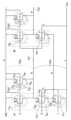
図1B欄の構成におけるデキャップ動作について、具体的な例を示す図2を参照してさらに説明する。図2は、半導体装置において、CMOS論理ゲートの出力信号レベルをハイ(H)に固定する構成例を示す回路図である。 The decap operation in the configuration in column B of FIG. 1 will be further described with reference to FIG. 2 showing a specific example. FIG. 2 is a circuit diagram showing a configuration example for fixing the output signal level of a CMOS logic gate to high (H) in a semiconductor device.
図2に示す半導体装置は、CMOS論理ゲート1Aと、CMOS論理ゲート1Aの出力ラインVo1に接続されるCMOS論理ゲート1Bと、を備えている。 The semiconductor device shown in FIG. 2 includes a
CMOS論理ゲート1Aは、電源ラインVddに接続されるPMOS11pと、PMOS11pのグランドラインVss側に接続されるNMOS11nと、を有するNOT回路として構成されている。 The
CMOS論理ゲート1Bは、電源ラインVddに接続されるPMOS12pと、PMOS12pのグランドラインVss側に接続されるNMOS12nと、を有するNOT回路として構成されている。CMOS論理ゲート1Bは、出力ラインVo2から信号を出力する。 The
図2においては、単純化されたCMOS論理ゲートの一例として、PMOSネットワーク1pが1つのPMOSで構成され、NMOSネットワーク1nが1つのNMOSで構成されるNOT回路を示している。 FIG. 2 shows, as an example of a simplified CMOS logic gate, a NOT circuit in which the PMOS network 1p is composed of one PMOS and the
さらに半導体装置は、CMOS論理ゲート1AおよびCMOS論理ゲート1Bの動作モードを、通常動作モードとデキャップ動作モードとに切り替えるためのMOS(モード切替用MOS)として、PMOS21p1、PMOS21p2、およびNMOS21nを備えている。これらのモード切替用MOSは、半導体装置のチップ面積が増大するのを抑制するために、小型のMOSとして形成されている。 Further, the semiconductor device includes PMOS 21p1, PMOS 21p2, and
PMOS21p1は、電源ラインVddとCMOS論理ゲート1Aの出力ラインVo1との間に接続されている。 The PMOS 21p1 is connected between the power supply line Vdd and the output line Vo1 of the
PMOS21p2は、電源ラインVddとCMOS論理ゲート1Bの出力ラインVo2との間に接続されている。 The PMOS 21p2 is connected between the power supply line Vdd and the output line Vo2 of the
NMOS21nは、CMOS論理ゲート1AのNMOS11nのソース、およびCMOS論理ゲート1BのNMOS12nのソースと、グランドラインVssと、の間に接続されている。図2に示すような出力信号レベルがハイ固定の場合、CMOS論理ゲート1A用とCMOS論理ゲート1B用とでNMOS21nを共通化することで、モード切替用MOSの数を少なくし、チップ面積の増大をより効果的に抑制している。 The
ここで、PMOSおよびNMOSは、各端子間に寄生容量を備えており、ゲートとソースとの間の寄生容量をCgs、ゲートとドレインとの間の寄生容量をCgd、ソースとバックゲートとの間の寄生容量をCsb、ドレインとバックゲートとの間の寄生容量をCdb、ゲートとバックゲートとの間の寄生容量をCgbと記載する。これらの記号を図2のPMOS21p1およびNMOS11nに明示するが、明示しない他のMOSについても同様の記号を用いるものとする。 Here, the PMOS and NMOS have parasitic capacitances between their respective terminals. Cgs is the parasitic capacitance between the gate and the source, Cgd is the parasitic capacitance between the gate and the drain, and Csb, the parasitic capacitance between the drain and the back gate is Cdb, and the parasitic capacitance between the gate and the back gate is Cgb. Although these symbols are clearly shown for PMOS 21p1 and
図2に示す構成において、モード切替用MOS、すなわち、PMOS21p1、PMOS21p2、およびNMOS21nの各ゲートにハイ(H)の制御信号を入力すると、PMOS21p1およびPMOS21p2はオフ、NMOS21nはオンとなる。従って、CMOS論理ゲート1AおよびCMOS論理ゲート1Bは、モード切替用MOSが設けられていないときと同様の、通常動作を行う(通常動作モード)。 In the configuration shown in FIG. 2, when a high (H) control signal is input to each gate of the mode switching MOS, that is, PMOS 21p1, PMOS 21p2, and
一方、PMOS21p1、PMOS21p2、およびNMOS21nの各ゲートにロー(L)の制御信号を入力すると、PMOS21p1およびPMOS21p2はオン、NMOS21nはオフとなる。これにより、CMOS論理ゲート1Aの出力ラインVo1は、PMOS21p1により電源ラインVddと導通されてハイ(H)に固定される。また、CMOS論理ゲート1Bの出力ラインVo2は、PMOS21p2により電源ラインVddと導通されてハイ(H)に固定される。従って、CMOS論理ゲート1Bの後段にある図示しないCMOS論理ゲートには、ハイ(H)の信号が入力されることになる。 On the other hand, when a low (L) control signal is input to each gate of PMOS 21p1, PMOS 21p2 and
出力ラインVo1は、CMOS論理ゲート1BのPMOS12pのゲート、およびNMOS12nのゲートに接続されているために、PMOS12pおよびNMOS12nのゲート入力はハイ(H)となる。同様に、CMOS論理ゲート1Aの前段の図示しないCMOS論理ゲートの出力ラインもハイ(H)に固定され、CMOS論理ゲート1AのPMOS11pおよびNMOS11nのゲート入力もハイ(H)になるものとする。 Since the output line Vo1 is connected to the gates of the
この場合、PMOS11pおよびPMOS12pのゲート端子、ソース端子、ドレイン端子、バックゲート端子は何れもハイ(H)となるために、PMOS11pおよびPMOS12pの寄生容量Cgs,Cgd,Csb,Cdb,Cgbは何れも活性化されない。 In this case, the gate terminals, source terminals, drain terminals, and back gate terminals of the
一方、NMOS11nおよびNMOS12nは、ゲート端子、ソース端子、およびドレイン端子がハイ(H)となり、バックゲート端子はグランドラインVssに接続されているためにロー(L)となる。これにより、ゲート端子とバックゲート端子との間の寄生容量Cgb、ソース端子とバックゲート端子との間の寄生容量Csb、およびドレイン端子とバックゲート端子との間の寄生容量Cdbが活性化され、それ以外の寄生容量Cgs,Cgdは活性化されない。 On the other hand,
また、PMOS21p1およびPMOS21p2は、ゲート端子にロー(L)の制御信号が入力され、ソース端子、ドレイン端子、およびバックゲート端子がハイ(H)である。これにより、ゲート端子とソース端子との間の寄生容量Cgs、ゲート端子とドレイン端子との間の寄生容量Cgd、およびゲート端子とバックゲート端子との間の寄生容量Cgbが活性化され、それ以外の寄生容量Csb,Cdbは活性化されない。 The PMOS 21p1 and PMOS 21p2 have gate terminals to which a low (L) control signal is input, and source terminals, drain terminals, and back gate terminals are high (H). As a result, the parasitic capacitance Cgs between the gate terminal and the source terminal, the parasitic capacitance Cgd between the gate terminal and the drain terminal, and the parasitic capacitance Cgb between the gate terminal and the back gate terminal are activated. are not activated.
さらに、NMOS21nは、ドレイン端子がハイ(H)であり、ゲート端子、ソース端子、およびバックゲート端子がロー(L)である。これにより、ゲート端子とドレイン端子との間の寄生容量Cgd、およびドレイン端子とバックゲート端子との間の寄生容量Cdbが活性化され、それ以外の寄生容量Cgs,Csb,Cgbは活性化されない。 Furthermore, the
ただし、モード切替用MOSは、上述したように小型のMOSとして形成されていて、活性化された寄生容量の合成容量への寄与が小さい。また、PMOS11pおよびPMOS12pの寄生容量は活性化されないために、その合成容量SCpは電源ラインVddとグランドラインVssとの間の容量に寄与しない。このために、図2に示すハイ固定の場合、NMOS11nおよびNMOS12nにおいて活性化された寄生容量の合成容量SCnが、電源ラインVddとグランドラインVssとの間の容量として支配的となる。こうして支配的となった合成容量SCnにより、電源ラインVddの電圧ゆらぎが抑制されて電源電圧が安定化される。
(出力信号レベルがロー固定の構成例)However, the mode switching MOS is formed as a small MOS as described above, and the contribution of the activated parasitic capacitance to the combined capacitance is small. Also, since the parasitic capacitances of
(Example of configuration in which the output signal level is fixed at low)
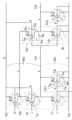
図2にはCMOS論理ゲートの出力信号レベルをハイ(H)に固定する例を示したが、これに限定されるものではなく、CMOS論理ゲートの出力信号レベルをロー(L)に固定しても構わない。図3は、半導体装置において、CMOS論理ゲートの出力信号レベルをロー(L)に固定する構成例を示す回路図である。 FIG. 2 shows an example in which the output signal level of the CMOS logic gate is fixed at high (H). I don't mind. FIG. 3 is a circuit diagram showing a configuration example for fixing the output signal level of a CMOS logic gate to low (L) in a semiconductor device.
図3に示す半導体装置は、図2に示した半導体装置と同様に、CMOS論理ゲート1Aと、CMOS論理ゲート1Aの出力ラインVo1に接続されるCMOS論理ゲート1Bと、を備えている。 The semiconductor device shown in FIG. 3, like the semiconductor device shown in FIG. 2, includes a
さらに図3に示す半導体装置は、モード切替用MOSとして、PMOS21p、NMOS21n1、およびNMOS21n2を備えている。これらのモード切替用MOSが小型(好ましくは最小サイズ)のMOSとして形成されているのは、図2の例と同様である。 Further, the semiconductor device shown in FIG. 3 includes
PMOS21pは、電源ラインVddと、CMOS論理ゲート1AのPMOS11pのソース、およびCMOS論理ゲート1BのPMOS12pのソースと、の間に接続されている。図3に示すようなロー固定の場合、CMOS論理ゲート1A用とCMOS論理ゲート1B用とでPMOS21pを共通化することで、モード切替用MOSの数を少なくし、チップ面積の増大をより効果的に抑制している。 The
NMOS21n1は、CMOS論理ゲート1Aの出力ラインVo1とグランドラインVssとの間に接続されている。 The NMOS 21n1 is connected between the output line Vo1 of the
NMOS21n2は、CMOS論理ゲート1Bの出力ラインVo2とグランドラインVssとの間に接続されている。 The NMOS 21n2 is connected between the output line Vo2 of the
図3に示す構成において、モード切替用MOS、すなわち、PMOS21p、NMOS21n1、およびNMOS21n2の各ゲートにロー(L)の制御信号を入力すると、PMOS21pはオン、NMOS21n1およびNMOS21n2はオフとなる。従って、CMOS論理ゲート1AおよびCMOS論理ゲート1Bは、モード切替用MOSが設けられていないときと同様の、通常動作を行う(通常動作モード)。 In the configuration shown in FIG. 3, when a low (L) control signal is input to each gate of the mode switching MOSs, that is,
一方、PMOS21p、NMOS21n1、およびNMOS21n2の各ゲートにハイ(H)の制御信号を入力すると、PMOS21pはオフ、NMOS21n1およびNMOS21n2はオンとなる。これにより、CMOS論理ゲート1Aの出力ラインVo1は、NMOS21n1によりグランドラインVssと導通されてロー(L)に固定される。また、CMOS論理ゲート1Bの出力ラインVo2は、NMOS21n2によりグランドラインVssと導通されてロー(L)に固定される。従って、CMOS論理ゲート1Bの後段にある図示しないCMOS論理ゲートには、ロー(L)の信号が入力されることになる。 On the other hand, when a high (H) control signal is input to each gate of
出力ラインVo1は、CMOS論理ゲート1BのPMOS12pのゲート、およびNMOS12nのゲートに接続されているために、PMOS12pおよびNMOS12nのゲート入力はロー(L)となる。同様に、CMOS論理ゲート1Aの前段の図示しないCMOS論理ゲートの出力ラインもロー(L)に固定され、CMOS論理ゲート1AのPMOS11pおよびNMOS11nのゲート入力もロー(L)になるものとする。 Since the output line Vo1 is connected to the gates of the
この場合、NMOS11nおよびNMOS12nのゲート端子、ソース端子、ドレイン端子、バックゲート端子は何れもロー(L)となるために、NMOS11nおよびNMOS12nの寄生容量Cgs,Cgd,Csb,Cdb,Cgbは何れも活性化されない。 In this case, the gate terminal, source terminal, drain terminal, and back gate terminal of
一方、PMOS11pおよびPMOS12pは、ゲート端子、ソース端子、およびドレイン端子がロー(L)となり、バックゲート端子は電源ラインVddに接続されているためにハイ(H)となる。これにより、ゲート端子とバックゲート端子との間の寄生容量Cgb、ソース端子とバックゲート端子との間の寄生容量Csb、およびドレイン端子とバックゲート端子との間の寄生容量Cdbが活性化され、それ以外の寄生容量Cgs,Cgdは活性化されない。 On the other hand,
また、NMOS21n1およびNMOS21n2は、ゲート端子にハイ(H)が入力され、ソース端子、ドレイン端子、およびバックゲート端子がロー(L)である。これにより、ゲート端子とソース端子との間の寄生容量Cgs、ゲート端子とドレイン端子との間の寄生容量Cgd、およびゲート端子とバックゲート端子との間の寄生容量Cgbが活性化され、それ以外の寄生容量Csb,Cdbは活性化されない。 The NMOS 21n1 and NMOS 21n2 have high (H) input to their gate terminals, and low (L) to their source terminals, drain terminals, and back gate terminals. As a result, the parasitic capacitance Cgs between the gate terminal and the source terminal, the parasitic capacitance Cgd between the gate terminal and the drain terminal, and the parasitic capacitance Cgb between the gate terminal and the back gate terminal are activated. are not activated.
さらに、PMOS21pは、ドレイン端子がロー(L)であり、ゲート端子、ソース端子、およびバックゲート端子がハイ(H)である。これにより、ゲート端子とドレイン端子との間の寄生容量Cgd、およびドレイン端子とバックゲート端子との間の寄生容量Cdbが活性化され、それ以外の寄生容量Cgs,Csb,Cgbは活性化されない。 Furthermore, the
ただし、モード切替用MOSは、上述したように活性化された寄生容量の合成容量への寄与が小さい。また、NMOS11nおよびNMOS12nの寄生容量は活性化されないために、その合成容量SCnは電源ラインVddとグランドラインVssとの間の容量に寄与しない。このために、図3に示すロー固定の場合、PMOS11pおよびPMOS12pにおいて活性化された寄生容量の合成容量SCpが、電源ラインVddとグランドラインVssとの間の容量として支配的となる。こうして支配的となった合成容量SCpにより、電源ラインVddの電圧ゆらぎが抑制されて電源電圧が安定化される。 However, the mode switching MOS contributes little to the combined capacitance of the parasitic capacitances activated as described above. Also, since the parasitic capacitances of
なお、一般的なCMOSの構成では、NMOSよりもPMOSの方がチップ上に形成される面積が大きい。このために、寄生容量の活性化は、NMOSに対して行うよりもPMOSに対して行う方が効果が高く、図3の構成の方が図2の構成よりも高い効果が得られると期待される。ただし、図2に示すハイ固定の構成と、図3に示すロー固定の構成との何れを採用するかは製造プロセス等にも依存するために、必要に応じて適切な方を選択すればよい。
(ハイ固定の具体的な回路例)Note that in a general CMOS configuration, a PMOS has a larger area on a chip than an NMOS. For this reason, activation of the parasitic capacitance is more effective in activating the PMOS than in the NMOS, and it is expected that the configuration of FIG. 3 is more effective than the configuration of FIG. be. However, since it depends on the manufacturing process and the like whether to adopt the high-fixed configuration shown in FIG. 2 or the low-fixed configuration shown in FIG. 3, the appropriate one may be selected as necessary. .
(Concrete circuit example of high fixation)
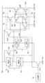
図4は、半導体装置において、サイズが大きいCMOS論理ゲートの出力信号レベルをハイ(H)に固定する構成例を示す回路図である。 FIG. 4 is a circuit diagram showing a configuration example for fixing the output signal level of a large-sized CMOS logic gate to high (H) in a semiconductor device.
図4に示す半導体装置は、CMOS論理ゲート1C、CMOS論理ゲート1D、およびCMOS論理ゲート1Eを備えている。 The semiconductor device shown in FIG. 4 includes a
CMOS論理ゲート1Cは、電源ラインVddに接続されるPMOSネットワーク1Cpと、PMOSネットワーク1CpのグランドラインVss側に接続されるNMOSネットワーク1Cnと、を有している。 The
CMOS論理ゲート1Dは、電源ラインVddに接続されるPMOSネットワーク1Dpと、PMOSネットワーク1DpとグランドラインVssとの間に接続されるNMOSネットワーク1Dnと、を有している。なお、CMOS論理ゲート1Dは、CMOS論理ゲート1Cと比較して、図4に模式的に示すようにサイズ(具体的には、チップ上の面積)が小さく、活性化可能な寄生容量が小さいものとする。 The
CMOS論理ゲート1Eは、電源ラインVddに接続されるPMOSネットワーク1Epと、PMOSネットワーク1EpのグランドラインVss側に接続されるNMOSネットワーク1Enと、を有している。PMOSネットワーク1Epは3つのPMOS13p1,13p2,13p3を備え、NMOSネットワーク1Enは3つのNMOS13n1,13n2,13n3を備えている。 The
図4に例示するCMOS論理ゲート1Eは、前段側のNOR回路1E1と、後段側のNOT回路1E2と、を組み合わせたOR回路として構成されている。NOR回路1E1には、CMOS論理ゲート1Cの出力信号と、CMOS論理ゲート1Dの出力信号と、が入力される。NOT回路1E2には、NOR回路1E1の出力信号が入力される。 The
NOR回路1E1は、CMOS論理ゲート1Cの出力ラインVo3に接続されるPMOS13p1およびNMOS13n1と、CMOS論理ゲート1Dの出力ラインVo4に接続されるPMOS13p2およびNMOS13n2と、を備えている。PMOS13p1、PMOS13p2、およびNMOS13n2は、電源ラインVddからグランドラインVss側へ向かって順に接続されている。また、NMOS13n1のドレインは、NOR回路1E1の出力ラインに接続されている。 The NOR circuit 1E1 includes PMOS 13p1 and NMOS 13n1 connected to the output line Vo3 of the
NOT回路1E2は、NOR回路1E1の出力ラインが接続されるPMOS13p3およびNMOS13n3を備えている。 The NOT circuit 1E2 has a PMOS 13p3 and an NMOS 13n3 to which the output line of the NOR circuit 1E1 is connected.
さらに半導体装置は、モード切替用MOSとして、PMOS21p1、PMOS21p2、およびNMOS21nを備えている。 Furthermore, the semiconductor device includes PMOS 21p1, PMOS 21p2, and
PMOS21p1は、電源ラインVddとCMOS論理ゲート1Cの出力ラインVo3との間に接続されている。 The PMOS 21p1 is connected between the power supply line Vdd and the output line Vo3 of the
PMOS21p2は、電源ラインVddとCMOS論理ゲート1Eの出力ラインVo5との間に接続されている。 The PMOS 21p2 is connected between the power supply line Vdd and the output line Vo5 of the
NMOS21nは、CMOS論理ゲート1CのNMOSネットワーク1Cnのソース、およびCMOS論理ゲート1EのNMOSネットワーク1Enのソースと、グランドラインVssと、の間に接続されている。CMOS論理ゲート1C用とCMOS論理ゲート1E用とでNMOS21nを共通化することで、モード切替用MOSの数を少なくし、チップ面積の増大をより効果的に抑制している。 The
一方、活性化可能な寄生容量が所定値よりも小さいCMOS論理ゲート1Dの出力ラインVo4と電源ラインVddとの間には、モード切替用MOSとしてのPMOSを設けておらず、CMOS論理ゲート1DはNMOS21nに接続されていない。こうして、寄生容量が所定値以上のCMOS論理ゲートだけに対してモード切替用MOSを設けることで、活性化可能な寄生容量の多くを有効に活用しながらモード切替用MOSの数を少なくすることができ、チップ面積の増大をさらに効果的に抑制している。 On the other hand, no PMOS as a mode switching MOS is provided between the output line Vo4 of the
PMOS21p1、PMOS21p2、およびNMOS21nの各ゲート端子は、半導体装置の入力端子31に接続されている。入力端子31の一例は、半導体装置をテストモードで動作させるためのテスト用入力端子(いわゆるテストピン)である。このような構成により、モード切替用MOSに含まれるPMOS21p1、PMOS21p2、およびNMOS21nが、1つの入力端子31から入力される制御信号により共通に制御されるために、入力端子の数を減らすことができる。 Each gate terminal of the PMOS 21p1, PMOS 21p2, and
CMOS論理ゲート1C,1D,1Eが、例えば、半導体装置をテストするためのテスト回路に含まれる場合、入力端子31にハイ(H)の制御信号を入力することで、テスト回路としての通常動作が行われる。一方、入力端子31にロー(L)の制御信号を入力することで、CMOS論理ゲート1C,1D,1Eはデキャップ動作を行ってデカップリングキャパシタDCと同様の機能を果たし、半導体装置がテスト回路以外の通常回路により動作するときに電源電圧を安定化する。 When the
また、CMOS論理ゲート1C,1D,1Eが、例えば、半導体装置の通常回路に含まれる場合、入力端子31にハイ(H)の制御信号を入力することで、通常回路としての通常動作が行われる。一方、入力端子31にロー(L)の制御信号を入力することで、CMOS論理ゲート1C,1D,1Eはデキャップ動作を行ってデカップリングキャパシタDCと同様の機能を果たし、半導体装置がテスト回路により動作するときに電源電圧を安定化する。なお、入力端子31がテスト用入力端子である場合には、入力端子31からの入力信号レベルを反転させてモード切替用MOSに供給するか、または図3を参照して示したようなロー固定の構成をCMOS論理ゲート1C,1D,1Eに対して適用すればよい。 When the
このように、通常回路が動作するときのテスト回路、テスト回路が動作するときの通常回路などの、使用していない回路であれば、適宜の回路の寄生容量を、デカップリングキャパシタDCと同様の機能を果たす容量として用いることが可能である。使用していない回路の他の例としては、半導体装置に設けられている各種の機能ブロックの内の、顧客アプリケーションで使用しない機能ブロック(リセット状態の機能ブロック等)が挙げられる。 In this way, if the circuit is not used, such as the test circuit when the circuit operates normally, the normal circuit when the test circuit operates, etc., the parasitic capacitance of the appropriate circuit can be reduced to the same value as the decoupling capacitor DC. It can be used as a functioning capacitor. Other examples of unused circuits include functional blocks (such as functional blocks in a reset state) that are not used by customer applications among various functional blocks provided in the semiconductor device.
第1の実施形態によれば、CMOS論理ゲート1の出力信号レベルをハイ(H)またはロー(L)に固定するためのモード切替用MOSを設けて、CMOS論理ゲート1の寄生容量を活性化することで、デカップリングキャパシタDCを別途設けることなく、電源ラインVddの電圧を安定化することができ、半導体装置のチップ面積の増大を抑制することができる。 According to the first embodiment, a mode switching MOS for fixing the output signal level of the
また、所定値以上の寄生容量を活性化できるCMOS論理ゲートに対応してMOSを追加することで、全てのCMOS論理ゲートに対してMOSを追加する場合よりも、追加するMOSの数を低減することができる。これにより、チップ面積の増大をさらに抑制しながら、有効な容量の活性化を行うことができる。
(第2の実施形態)By adding MOSs corresponding to CMOS logic gates capable of activating a parasitic capacitance of a predetermined value or more, the number of MOSs to be added is reduced compared to adding MOSs to all CMOS logic gates. be able to. As a result, it is possible to effectively activate the capacitance while further suppressing an increase in the chip area.
(Second embodiment)
図5は、本実施形態に係わる半導体装置において、入力信号レベルがハイ(H)に固定されても出力信号レベルがハイ(H)に固定されないCMOS論理ゲートに対して、出力信号レベルをハイ(H)に固定する構成例を示す回路図である。 FIG. 5 shows, in the semiconductor device according to the present embodiment, a CMOS logic gate whose output signal level is not fixed to high (H) even if the input signal level is fixed to high (H). H) is a circuit diagram showing a configuration example fixed.
第2の実施形態において、第1の実施形態と同様である部分については同一の符号を付すなどして説明を適宜省略し、主として異なる点について説明する。 In the second embodiment, parts that are the same as those in the first embodiment are assigned the same reference numerals, and the description thereof is omitted as appropriate, and mainly the points of difference will be described.
本実施形態は、モード切替用MOSを設けるか否かを、CMOS論理ゲートのサイズに応じて決める代わりに、入力信号に対してどのような信号を出力するCMOS論理ゲートであるかに応じて決めたものとなっている。 In this embodiment, whether or not to provide a mode switching MOS is determined according to what kind of signal the CMOS logic gate outputs in response to an input signal, instead of determining according to the size of the CMOS logic gate. It has become a thing.
図5に示す半導体装置は、図4に示す半導体装置と比較して、CMOS論理ゲート1Dに対応するPMOS21p3を追加し、CMOS論理ゲート1Eに対応するPMOS21p2を省略している。本実施形態においては、CMOS論理ゲートのサイズを区別することなく、サイズが小さいCMOS論理ゲート(ここでは、CMOS論理ゲート1D)に対してもモード切替用MOSを設けている。 Compared to the semiconductor device shown in FIG. 4, the semiconductor device shown in FIG. 5 adds a PMOS 21p3 corresponding to the
PMOS21p3は、電源ラインVddとCMOS論理ゲート1Dの出力ラインVo4との間に接続されている。 The PMOS 21p3 is connected between the power supply line Vdd and the output line Vo4 of the
NMOS21nは、CMOS論理ゲート1CのNMOSネットワーク1Cnのソース、およびCMOS論理ゲート1DのNMOSネットワーク1Dnのソースと、グランドラインVssと、の間に接続されている。CMOS論理ゲート1C用とCMOS論理ゲート1D用とでNMOS21nを共通化することで、モード切替用MOSの数を少なくし、チップ面積の増大をより効果的に抑制しているのは、上述と同様である。 The
また、CMOS論理ゲート1EのNMOSネットワーク1Enのソースは、グランドラインVssに接続されている。 Also, the source of the NMOS network 1En of the
ここで、PMOS21p2を省略したのは、次の理由による。すなわち、入力端子31からロー(L)の制御信号を入力すれば、CMOS論理ゲート1CとCMOS論理ゲート1Dの出力は何れもハイ(H)に固定され、OR回路として構成されているCMOS論理ゲート1Eの出力は自動的にハイ(H)に固定される。従って、CMOS論理ゲート1Cの出力信号レベルをハイ(H)に固定するためのPMOS21p2を設ける必要がないからである。 The reason why the PMOS 21p2 is omitted here is as follows. That is, when a low (L) control signal is input from the
OR回路に限らず、AND回路、XNOR回路など、複数の入力信号レベルが何れもハイ(H)である場合に出力信号レベルがハイ(H)となるCMOS論理ゲートについては、モード切替用MOSを設けなくても構わない。従って、入力信号レベルがハイ(H)に固定されても出力信号レベルがハイ(H)に固定されるとは限らないCMOS論理ゲートだけに対して、モード切替用MOSを設ければよい。 Not only OR circuits, but also AND circuits, XNOR circuits, and other CMOS logic gates in which the output signal level is high (H) when all of a plurality of input signal levels are high (H), a mode switching MOS is used. Optional. Therefore, the mode switching MOS should be provided only for CMOS logic gates whose output signal level is not necessarily fixed to high (H) even if the input signal level is fixed to high (H).
また、図3に示したようなロー固定の構成を、図5の構成に適用しても構わないことは上述と同様である。この場合には、入力信号レベルがロー(L)に固定されても出力信号レベルがロー(L)に固定されるとは限らないCMOS論理ゲートだけに対して、モード切替用MOSを設ければよい。 Also, the low-fixed configuration as shown in FIG. 3 may be applied to the configuration in FIG. 5, as described above. In this case, if the mode switching MOS is provided only for the CMOS logic gate whose output signal level is not necessarily fixed to low (L) even if the input signal level is fixed to low (L). good.
第2の実施形態によれば、第1の実施形態とほぼ同様の効果を奏するとともに、入力信号レベルがハイ(H)またはロー(L)に固定されても出力信号レベルがハイ(H)またはロー(L)に固定されないCMOS論理ゲートだけにモード切替用MOSを設けることで、追加するMOSの数を低減してチップ面積の増大を抑制しながら、寄生容量を活性化して電源電圧を安定化することができる。
(第3の実施形態)According to the second embodiment, substantially the same effects as those of the first embodiment are obtained. By providing mode-switching MOS only for CMOS logic gates that are not fixed to low (L), the number of MOSs to be added is reduced, suppressing an increase in chip area, while activating parasitic capacitance and stabilizing the power supply voltage. can do.
(Third Embodiment)
図6は、本実施形態に係わる半導体装置において、パワーオフモードとして利用できるように制御信号の入力端子を複数設けた場合の、出力信号レベルをハイ(H)に固定する構成例を示す回路図である。 FIG. 6 is a circuit diagram showing a configuration example for fixing the output signal level to high (H) when a plurality of control signal input terminals are provided so that the semiconductor device according to the present embodiment can be used as a power-off mode. is.
第3の実施形態において、第1,2の実施形態と同様である部分については同一の符号を付すなどして説明を適宜省略し、主として異なる点について説明する。 In the third embodiment, parts that are the same as those in the first and second embodiments are denoted by the same reference numerals, and descriptions thereof are omitted as appropriate, and differences are mainly described.
図6に示す本実施形態の半導体装置は、図5に示した半導体装置と概略同様に構成されているが、モード切替用MOSの入力端子を、NMOSとPMOSとの2系統に分けている点が異なっている。 The semiconductor device of the present embodiment shown in FIG. 6 is configured in substantially the same manner as the semiconductor device shown in FIG. is different.
すなわち、PMOS21p1およびPMOS21p3のゲートは入力端子31Aに接続され、NMOS21nのゲートは入力端子31Bに接続されている。入力端子31Bの一例はテスト用入力端子であり、入力端子31Aの一例はパワーオフ用入力端子である。 That is, the gates of PMOS 21p1 and PMOS 21p3 are connected to input terminal 31A, and the gate of
入力端子31Aおよび入力端子31Bからハイ(H)の制御信号を入力したときの半導体装置の作用は、図5の入力端子31にハイ(H)の制御信号を入力したときの半導体装置の作用と同じである。 The operation of the semiconductor device when a high (H) control signal is input from the
また、入力端子31Aおよび入力端子31Bからロー(L)の制御信号を入力したときの半導体装置の作用は、図5の入力端子31にロー(L)の制御信号を入力したときの半導体装置の作用と同じである。 The operation of the semiconductor device when a low (L) control signal is input from the
一方、入力端子31Aからハイ(H)の制御信号を入力し、入力端子31Bからロー(L)の制御信号を入力すると、モード切替用MOSであるPMOS21p1、PMOS21p3、NMOS21nは何れもオフとなり(パワーオフ動作モード)、電源ラインVddから、PMOS21p1、PMOS21p3、NMOS21nを経由してグランドラインVss側へ流れるリーク電流を低減することができる。 On the other hand, when a high (H) control signal is input from the
なお、モード切替用MOSの入力端子をNMOSとPMOSとの2系統に分ける本実施形態の構成を、図3に示したようなロー固定の構成に適用しても構わないことは勿論である。 It goes without saying that the configuration of this embodiment in which the input terminals of the mode switching MOS are divided into two systems, NMOS and PMOS, may be applied to the low-fixed configuration as shown in FIG.
第3の実施形態によれば、第2の実施形態とほぼ同様の効果を奏するとともに、モード切替用MOSのNMOSとPMOSとが独立に制御されるために、パワーオフ動作が可能となり、リーク電流を低減することができる。 According to the third embodiment, substantially the same effects as those of the second embodiment are obtained, and since the NMOS and PMOS of the mode switching MOS are independently controlled, the power-off operation becomes possible and the leakage current is reduced. can be reduced.
本発明のいくつかの実施形態を説明したが、これらの実施形態は、例として示したものであり、発明の範囲を限定することは意図していない。これら新規な実施形態は、その他の様々な形態で実施されることが可能であり、発明の要旨を逸脱しない範囲で、種々の省略、置き換え、変更を行うことができる。これら実施形態やその変形は、発明の範囲や要旨に含まれると共に、特許請求の範囲に記載された発明とその均等の範囲に含まれる。 While several embodiments of the invention have been described, these embodiments are provided by way of example and are not intended to limit the scope of the invention. These novel embodiments can be implemented in various other forms, and various omissions, replacements, and modifications can be made without departing from the scope of the invention. These embodiments and modifications thereof are included in the scope and gist of the invention, and are included in the scope of the invention described in the claims and equivalents thereof.
1,1A~1E CMOS論理ゲート、1p,1Cp,1Dp,1Ep PMOSネットワーク、1n,1Cn,1Dn,1En NMOSネットワーク、31,31A,31B 入力端子、Cgs,Cgd,Csb,Cdb,Cgb 寄生容量、Vdd 電源ライン、Vss グランドライン1, 1A to 1E CMOS logic gate, 1p, 1Cp, 1Dp, 1Ep PMOS network, 1n, 1Cn, 1Dn, 1En NMOS network, 31, 31A, 31B input terminal, Cgs, Cgd, Csb, Cdb, Cgb parasitic capacitance, Vdd Power supply line, Vss ground line
Claims (6)
Translated fromJapanese前記電源ラインに接続されるP型MOSFETネットワークと、前記P型MOSFETネットワークの前記グランドライン側に接続されるN型MOSFETネットワークと、を有する複数のCMOS論理ゲートと、
前記複数のCMOS論理ゲートの出力信号レベルを固定することにより、前記複数のCMOS論理ゲートの寄生容量に電位差を与えるMOSFETと、
を有し、
前記MOSFETは、
前記電源ラインと前記複数のCMOS論理ゲートの複数の出力ラインとの間に接続される複数のP型MOSFETと、
前記複数のCMOS論理ゲートと前記グランドラインとの間に共通して接続されるN型MOSFETと、
を有し、
前記複数のP型MOSFETの複数のゲート端子にローの制御信号を入力し、かつ前記N型MOSFETのゲート端子にローの制御信号を入力することで、前記複数のCMOS論理ゲートの出力信号レベルをハイに固定し、前記複数のCMOS論理ゲートの複数のN型MOSFETネットワークの寄生容量を活性化する半導体装置。a power supply line and a ground line;
a plurality of CMOS logic gates having a P-type MOSFET network connected to the power supply line and an N-type MOSFET network connected to the ground line side of the P-type MOSFET network;
a MOSFET that provides a potential difference to parasitic capacitances ofthe plurality of CMOS logic gates by fixing output signal levels ofthe plurality of CMOS logic gates;
has
The MOSFET is
a plurality of P-type MOSFETs connected between the power supply line and the plurality of output lines of the plurality of CMOS logic gates;
an N-type MOSFET commonly connected between the plurality of CMOS logic gates and the ground line;
has
By inputting a low control signal to the gate terminals of the plurality of P-type MOSFETs and inputting a low control signal to the gate terminals of the N-type MOSFETs, the output signal levels of the plurality of CMOS logic gates are adjusted. A semiconductor devicethat is tied high to activate the parasitic capacitance of a plurality of N-type MOSFET networks of said plurality of CMOS logic gates .
前記複数のP型MOSFETの複数のゲート端子、および前記N型MOSFETのゲート端子は、前記入力端子に接続されている、請求項1に記載の半導体装置。 2. The semiconductor device according to claim 1, wherein a plurality of gate terminals of said plurality of P-type MOSFETs and a gate terminal of said N-type MOSFET are connected to said input terminal.
外部から第2の制御信号を入力する第2の入力端子と、 a second input terminal for inputting a second control signal from the outside;
をさらに有し、 further having
前記複数のP型MOSFETの複数のゲート端子は、前記第1の入力端子に接続され、 a plurality of gate terminals of the plurality of P-type MOSFETs are connected to the first input terminal;
前記N型MOSFETのゲート端子は、前記第2の入力端子に接続されている、請求項1に記載の半導体装置。 2. The semiconductor device according to claim 1, wherein said N-type MOSFET has a gate terminal connected to said second input terminal.
前記電源ラインに接続されるP型MOSFETネットワークと、前記P型MOSFETネットワークの前記グランドライン側に接続されるN型MOSFETネットワークと、を有する複数のCMOS論理ゲートと、 a plurality of CMOS logic gates having a P-type MOSFET network connected to the power supply line and an N-type MOSFET network connected to the ground line side of the P-type MOSFET network;
前記複数のCMOS論理ゲートの出力信号レベルを固定することにより、前記複数のCMOS論理ゲートの寄生容量に電位差を与えるMOSFETと、 a MOSFET that provides a potential difference to parasitic capacitances of the plurality of CMOS logic gates by fixing output signal levels of the plurality of CMOS logic gates;
を有し、 has
前記MOSFETは、 The MOSFET is
前記電源ラインと前記複数のCMOS論理ゲートとの間に共通して接続されるP型MOSFETと、 a P-type MOSFET commonly connected between the power supply line and the plurality of CMOS logic gates;
前記複数のCMOS論理ゲートの複数の出力ラインと前記グランドラインとの間に接続される複数のN型MOSFETと、 a plurality of N-type MOSFETs connected between the plurality of output lines of the plurality of CMOS logic gates and the ground line;
を有し、 has
前記P型MOSFETのゲート端子にハイの制御信号を入力し、かつ前記複数のN型MOSFETの複数のゲート端子にハイの制御信号を入力することで、前記複数のCMOS論理ゲートの出力信号レベルをローに固定し、前記複数のCMOS論理ゲートの複数のP型MOSFETネットワークの寄生容量を活性化する半導体装置。 By inputting a high control signal to the gate terminal of the P-type MOSFET and inputting a high control signal to the plurality of gate terminals of the plurality of N-type MOSFETs, the output signal levels of the plurality of CMOS logic gates are adjusted to A semiconductor device that is tied low to activate parasitic capacitances of a plurality of P-type MOSFET networks of said plurality of CMOS logic gates.
前記P型MOSFETのゲート端子、および前記複数のN型MOSFETの複数のゲート端子は、前記入力端子に接続されている、請求項4に記載の半導体装置。 5. The semiconductor device according to claim 4, wherein a gate terminal of said P-type MOSFET and a plurality of gate terminals of said plurality of N-type MOSFETs are connected to said input terminal.
外部から第2の制御信号を入力する第2の入力端子と、 a second input terminal for inputting a second control signal from the outside;
をさらに有し、 further having
前記P型MOSFETのゲート端子は、前記第1の入力端子に接続され、 a gate terminal of the P-type MOSFET is connected to the first input terminal;
前記複数のN型MOSFETの複数のゲート端子は、前記第2の入力端子に接続されている、請求項4に記載の半導体装置。 5. The semiconductor device according to claim 4, wherein a plurality of gate terminals of said plurality of N-type MOSFETs are connected to said second input terminal.
Priority Applications (2)
| Application Number | Priority Date | Filing Date | Title |
|---|---|---|---|
| JP2020152703AJP7332556B2 (en) | 2020-09-11 | 2020-09-11 | semiconductor equipment |
| US17/463,331US11522541B2 (en) | 2020-09-11 | 2021-08-31 | Semiconductor device |
Applications Claiming Priority (1)
| Application Number | Priority Date | Filing Date | Title |
|---|---|---|---|
| JP2020152703AJP7332556B2 (en) | 2020-09-11 | 2020-09-11 | semiconductor equipment |
Publications (2)
| Publication Number | Publication Date |
|---|---|
| JP2022047011A JP2022047011A (en) | 2022-03-24 |
| JP7332556B2true JP7332556B2 (en) | 2023-08-23 |
Family
ID=80627198
Family Applications (1)
| Application Number | Title | Priority Date | Filing Date |
|---|---|---|---|
| JP2020152703AActiveJP7332556B2 (en) | 2020-09-11 | 2020-09-11 | semiconductor equipment |
Country Status (2)
| Country | Link |
|---|---|
| US (1) | US11522541B2 (en) |
| JP (1) | JP7332556B2 (en) |
Citations (3)
| Publication number | Priority date | Publication date | Assignee | Title |
|---|---|---|---|---|
| JP2002164775A (en) | 2000-09-18 | 2002-06-07 | Sony Corp | Transistor circuit |
| JP2004147175A (en) | 2002-10-25 | 2004-05-20 | Renesas Technology Corp | Semiconductor device |
| JP2006080675A (en) | 2004-09-07 | 2006-03-23 | Toshiba Microelectronics Corp | Semiconductor integrated circuit and layout design method thereof |
Family Cites Families (6)
| Publication number | Priority date | Publication date | Assignee | Title |
|---|---|---|---|---|
| JPS6161437A (en) | 1984-09-03 | 1986-03-29 | Toshiba Corp | Semiconductor integrated circuit device |
| US6307236B1 (en)* | 1996-04-08 | 2001-10-23 | Hitachi, Ltd. | Semiconductor integrated circuit device |
| TW546615B (en)* | 2000-11-22 | 2003-08-11 | Hitachi Ltd | Display device having an improved voltage level converter circuit |
| JP5287048B2 (en) | 2008-09-01 | 2013-09-11 | 富士電機株式会社 | Micro power module |
| JP2012159370A (en) | 2011-01-31 | 2012-08-23 | Renesas Electronics Corp | Semiconductor device and test method thereof |
| WO2012153377A1 (en) | 2011-05-06 | 2012-11-15 | 富士通株式会社 | Semiconductor integrated circuit and method for controlling same |
- 2020
- 2020-09-11JPJP2020152703Apatent/JP7332556B2/enactiveActive
- 2021
- 2021-08-31USUS17/463,331patent/US11522541B2/enactiveActive
Patent Citations (3)
| Publication number | Priority date | Publication date | Assignee | Title |
|---|---|---|---|---|
| JP2002164775A (en) | 2000-09-18 | 2002-06-07 | Sony Corp | Transistor circuit |
| JP2004147175A (en) | 2002-10-25 | 2004-05-20 | Renesas Technology Corp | Semiconductor device |
| JP2006080675A (en) | 2004-09-07 | 2006-03-23 | Toshiba Microelectronics Corp | Semiconductor integrated circuit and layout design method thereof |
Also Published As
| Publication number | Publication date |
|---|---|
| US20220085807A1 (en) | 2022-03-17 |
| JP2022047011A (en) | 2022-03-24 |
| US11522541B2 (en) | 2022-12-06 |
Similar Documents
| Publication | Publication Date | Title |
|---|---|---|
| US7746152B2 (en) | Switch circuit device, and wireless circuit device and sampling circuit device employing the same | |
| US7605636B2 (en) | Power gating structure, semiconductor including the same and method of controlling a power gating | |
| US20090040671A1 (en) | Power clamp for on-chip ESD protection | |
| US20200035670A1 (en) | Electrostatic discharge protection apparatus for integrated circuit | |
| US7362136B2 (en) | Dual voltage single gate oxide I/O circuit with high voltage stress tolerance | |
| US5635860A (en) | Overvoltage-tolerant self-biasing CMOS output buffer | |
| JP2011029912A (en) | Reference voltage circuit and electronic device | |
| US10627847B2 (en) | Bias current circuit operating at high and low voltages | |
| US9379707B2 (en) | Decoupling circuit and semiconductor integrated circuit | |
| KR970060217A (en) | Output circuit, circuit for reducing leakage current, method for selectively switching transistor and semiconductor memory | |
| US8466722B2 (en) | Startup and protection circuitry for thin oxide output stage | |
| US20060097769A1 (en) | Level shift circuit and semiconductor circuit device including the level shift circuit | |
| US8169250B2 (en) | Signal level conversion circuit | |
| US20080136497A1 (en) | Tunable voltage controller for a sub-circuit and method of operating the same | |
| US7514960B2 (en) | Level shifter circuit | |
| US10965116B2 (en) | Overvoltage-proof circuit capable of preventing damage caused by overvoltage | |
| US8049555B2 (en) | Low leakage sampling switch | |
| JP7332556B2 (en) | semiconductor equipment | |
| CN113093852B (en) | Electric leakage compensation circuit | |
| KR102845796B1 (en) | Delay circuit | |
| KR102101537B1 (en) | Tie-High/Tie-Low Circuit | |
| US6850094B2 (en) | Semiconductor integrated circuit having a plurality of threshold voltages | |
| US7791224B2 (en) | Method and apparatus for providing a voltage to a circuit | |
| US11070206B2 (en) | Logic circuit | |
| TW201830863A (en) | Power-on control circuit and input/output control circuit |
Legal Events
| Date | Code | Title | Description |
|---|---|---|---|
| A621 | Written request for application examination | Free format text:JAPANESE INTERMEDIATE CODE: A621 Effective date:20220623 | |
| A977 | Report on retrieval | Free format text:JAPANESE INTERMEDIATE CODE: A971007 Effective date:20230421 | |
| A131 | Notification of reasons for refusal | Free format text:JAPANESE INTERMEDIATE CODE: A131 Effective date:20230425 | |
| A521 | Request for written amendment filed | Free format text:JAPANESE INTERMEDIATE CODE: A523 Effective date:20230621 | |
| TRDD | Decision of grant or rejection written | ||
| A01 | Written decision to grant a patent or to grant a registration (utility model) | Free format text:JAPANESE INTERMEDIATE CODE: A01 Effective date:20230718 | |
| A61 | First payment of annual fees (during grant procedure) | Free format text:JAPANESE INTERMEDIATE CODE: A61 Effective date:20230810 | |
| R150 | Certificate of patent or registration of utility model | Ref document number:7332556 Country of ref document:JP Free format text:JAPANESE INTERMEDIATE CODE: R150 |