JP7330181B2 - High-pressure steam annealing treatment equipment - Google Patents
High-pressure steam annealing treatment equipmentDownload PDFInfo
- Publication number
- JP7330181B2 JP7330181B2JP2020526392AJP2020526392AJP7330181B2JP 7330181 B2JP7330181 B2JP 7330181B2JP 2020526392 AJP2020526392 AJP 2020526392AJP 2020526392 AJP2020526392 AJP 2020526392AJP 7330181 B2JP7330181 B2JP 7330181B2
- Authority
- JP
- Japan
- Prior art keywords
- cassette
- chamber body
- batch processing
- bottom wall
- processing chamber
- Prior art date
- Legal status (The legal status is an assumption and is not a legal conclusion. Google has not performed a legal analysis and makes no representation as to the accuracy of the status listed.)
- Active
Links
Images


Classifications
- H—ELECTRICITY
- H01—ELECTRIC ELEMENTS
- H01L—SEMICONDUCTOR DEVICES NOT COVERED BY CLASS H10
- H01L21/00—Processes or apparatus adapted for the manufacture or treatment of semiconductor or solid state devices or of parts thereof
- H01L21/67—Apparatus specially adapted for handling semiconductor or electric solid state devices during manufacture or treatment thereof; Apparatus specially adapted for handling wafers during manufacture or treatment of semiconductor or electric solid state devices or components ; Apparatus not specifically provided for elsewhere
- H01L21/67005—Apparatus not specifically provided for elsewhere
- H01L21/67011—Apparatus for manufacture or treatment
- H01L21/67098—Apparatus for thermal treatment
- H01L21/67109—Apparatus for thermal treatment mainly by convection
- H—ELECTRICITY
- H01—ELECTRIC ELEMENTS
- H01L—SEMICONDUCTOR DEVICES NOT COVERED BY CLASS H10
- H01L21/00—Processes or apparatus adapted for the manufacture or treatment of semiconductor or solid state devices or of parts thereof
- H01L21/67—Apparatus specially adapted for handling semiconductor or electric solid state devices during manufacture or treatment thereof; Apparatus specially adapted for handling wafers during manufacture or treatment of semiconductor or electric solid state devices or components ; Apparatus not specifically provided for elsewhere
- H01L21/67005—Apparatus not specifically provided for elsewhere
- H01L21/67011—Apparatus for manufacture or treatment
- H01L21/67098—Apparatus for thermal treatment
- H01L21/67103—Apparatus for thermal treatment mainly by conduction
- H—ELECTRICITY
- H01—ELECTRIC ELEMENTS
- H01L—SEMICONDUCTOR DEVICES NOT COVERED BY CLASS H10
- H01L21/00—Processes or apparatus adapted for the manufacture or treatment of semiconductor or solid state devices or of parts thereof
- H01L21/67—Apparatus specially adapted for handling semiconductor or electric solid state devices during manufacture or treatment thereof; Apparatus specially adapted for handling wafers during manufacture or treatment of semiconductor or electric solid state devices or components ; Apparatus not specifically provided for elsewhere
- H01L21/67005—Apparatus not specifically provided for elsewhere
- H01L21/67011—Apparatus for manufacture or treatment
- H01L21/67126—Apparatus for sealing, encapsulating, glassing, decapsulating or the like
- H—ELECTRICITY
- H01—ELECTRIC ELEMENTS
- H01L—SEMICONDUCTOR DEVICES NOT COVERED BY CLASS H10
- H01L21/00—Processes or apparatus adapted for the manufacture or treatment of semiconductor or solid state devices or of parts thereof
- H01L21/67—Apparatus specially adapted for handling semiconductor or electric solid state devices during manufacture or treatment thereof; Apparatus specially adapted for handling wafers during manufacture or treatment of semiconductor or electric solid state devices or components ; Apparatus not specifically provided for elsewhere
- H01L21/67005—Apparatus not specifically provided for elsewhere
- H01L21/67011—Apparatus for manufacture or treatment
- H01L21/67155—Apparatus for manufacturing or treating in a plurality of work-stations
- H01L21/6719—Apparatus for manufacturing or treating in a plurality of work-stations characterized by the construction of the processing chambers, e.g. modular processing chambers
- H—ELECTRICITY
- H01—ELECTRIC ELEMENTS
- H01L—SEMICONDUCTOR DEVICES NOT COVERED BY CLASS H10
- H01L21/00—Processes or apparatus adapted for the manufacture or treatment of semiconductor or solid state devices or of parts thereof
- H01L21/67—Apparatus specially adapted for handling semiconductor or electric solid state devices during manufacture or treatment thereof; Apparatus specially adapted for handling wafers during manufacture or treatment of semiconductor or electric solid state devices or components ; Apparatus not specifically provided for elsewhere
- H01L21/67005—Apparatus not specifically provided for elsewhere
- H01L21/67242—Apparatus for monitoring, sorting or marking
- H01L21/67248—Temperature monitoring
- H—ELECTRICITY
- H01—ELECTRIC ELEMENTS
- H01L—SEMICONDUCTOR DEVICES NOT COVERED BY CLASS H10
- H01L21/00—Processes or apparatus adapted for the manufacture or treatment of semiconductor or solid state devices or of parts thereof
- H01L21/67—Apparatus specially adapted for handling semiconductor or electric solid state devices during manufacture or treatment thereof; Apparatus specially adapted for handling wafers during manufacture or treatment of semiconductor or electric solid state devices or components ; Apparatus not specifically provided for elsewhere
- H01L21/673—Apparatus specially adapted for handling semiconductor or electric solid state devices during manufacture or treatment thereof; Apparatus specially adapted for handling wafers during manufacture or treatment of semiconductor or electric solid state devices or components ; Apparatus not specifically provided for elsewhere using specially adapted carriers or holders; Fixing the workpieces on such carriers or holders
- H01L21/6732—Vertical carrier comprising wall type elements whereby the substrates are horizontally supported, e.g. comprising sidewalls
- H—ELECTRICITY
- H01—ELECTRIC ELEMENTS
- H01L—SEMICONDUCTOR DEVICES NOT COVERED BY CLASS H10
- H01L21/00—Processes or apparatus adapted for the manufacture or treatment of semiconductor or solid state devices or of parts thereof
- H01L21/67—Apparatus specially adapted for handling semiconductor or electric solid state devices during manufacture or treatment thereof; Apparatus specially adapted for handling wafers during manufacture or treatment of semiconductor or electric solid state devices or components ; Apparatus not specifically provided for elsewhere
- H01L21/673—Apparatus specially adapted for handling semiconductor or electric solid state devices during manufacture or treatment thereof; Apparatus specially adapted for handling wafers during manufacture or treatment of semiconductor or electric solid state devices or components ; Apparatus not specifically provided for elsewhere using specially adapted carriers or holders; Fixing the workpieces on such carriers or holders
- H01L21/6735—Closed carriers
- H01L21/67389—Closed carriers characterised by atmosphere control
- H—ELECTRICITY
- H01—ELECTRIC ELEMENTS
- H01L—SEMICONDUCTOR DEVICES NOT COVERED BY CLASS H10
- H01L21/00—Processes or apparatus adapted for the manufacture or treatment of semiconductor or solid state devices or of parts thereof
- H01L21/67—Apparatus specially adapted for handling semiconductor or electric solid state devices during manufacture or treatment thereof; Apparatus specially adapted for handling wafers during manufacture or treatment of semiconductor or electric solid state devices or components ; Apparatus not specifically provided for elsewhere
- H01L21/683—Apparatus specially adapted for handling semiconductor or electric solid state devices during manufacture or treatment thereof; Apparatus specially adapted for handling wafers during manufacture or treatment of semiconductor or electric solid state devices or components ; Apparatus not specifically provided for elsewhere for supporting or gripping
- H01L21/687—Apparatus specially adapted for handling semiconductor or electric solid state devices during manufacture or treatment thereof; Apparatus specially adapted for handling wafers during manufacture or treatment of semiconductor or electric solid state devices or components ; Apparatus not specifically provided for elsewhere for supporting or gripping using mechanical means, e.g. chucks, clamps or pinches
- H01L21/68714—Apparatus specially adapted for handling semiconductor or electric solid state devices during manufacture or treatment thereof; Apparatus specially adapted for handling wafers during manufacture or treatment of semiconductor or electric solid state devices or components ; Apparatus not specifically provided for elsewhere for supporting or gripping using mechanical means, e.g. chucks, clamps or pinches the wafers being placed on a susceptor, stage or support
- H01L21/68792—Apparatus specially adapted for handling semiconductor or electric solid state devices during manufacture or treatment thereof; Apparatus specially adapted for handling wafers during manufacture or treatment of semiconductor or electric solid state devices or components ; Apparatus not specifically provided for elsewhere for supporting or gripping using mechanical means, e.g. chucks, clamps or pinches the wafers being placed on a susceptor, stage or support characterised by the construction of the shaft
Landscapes
- Engineering & Computer Science (AREA)
- Physics & Mathematics (AREA)
- Condensed Matter Physics & Semiconductors (AREA)
- General Physics & Mathematics (AREA)
- Manufacturing & Machinery (AREA)
- Computer Hardware Design (AREA)
- Microelectronics & Electronic Packaging (AREA)
- Power Engineering (AREA)
- Chemical Vapour Deposition (AREA)
- Container, Conveyance, Adherence, Positioning, Of Wafer (AREA)
Description
Translated fromJapanese[0001] 本開示の実施形態は、概して、集積回路の製造に関し、具体的には、一又は複数の半導体基板をアニールするための装置に関する。 [0001] Embodiments of the present disclosure relate generally to the manufacture of integrated circuits and, more particularly, to an apparatus for annealing one or more semiconductor substrates.
関連技術の記載
[0002] メモリデバイス、論理デバイス、マイクロプロセッサなどの半導体デバイスの形成は、半導体基板上への一又は複数の膜の堆積を伴う。膜は、半導体デバイスを製造するために必要な回路を作成するために使用される。アニーリングは、堆積された膜の電気的特性を改善するために、堆積された膜に対して様々な効果を達成するために使用される熱処理プロセスである。例えば、アニーリングを使用して、ドーパントを活性化し、堆積膜を高密度化し、又は成長膜の状態を変化させることができる。Description of the Related Art [0002] The formation of semiconductor devices, such as memory devices, logic devices, microprocessors, etc., involves the deposition of one or more films on a semiconductor substrate. Films are used to create the circuits needed to manufacture semiconductor devices. Annealing is a heat treatment process used to achieve various effects on deposited films to improve their electrical properties. For example, annealing can be used to activate dopants, densify the deposited film, or change the state of the grown film.
[0003] 半導体デバイスの幾何形状は、数十年前の導入以来、サイズが劇的に縮小されてきた。デバイス密度の増加は、減少した空間寸法を有する構造的特徴をもたらした。例えば、高アスペクト比(深さ対幅の比)の間隙及びトレンチにおいて、現代の半導体デバイスの構造上の特徴は、間隙を材料で充填することが極めて困難になる程度まで狭まっており、特に、間隙を充填する材料の特性を確実に制御することができない点で、極めて困難になってきている。バルク堆積材料の特性を改善するのに適した従来のアニーリング処理は、高アスペクト比の特徴で堆積された材料の特性を改善する能力を実証していない。 [0003] Semiconductor device geometries have dramatically decreased in size since their introduction several decades ago. Increased device density has resulted in structural features with reduced spatial dimensions. For example, in high aspect ratio (depth-to-width ratio) gaps and trenches, the structural features of modern semiconductor devices have narrowed to the point where filling the gaps with material becomes extremely difficult, especially: It is becoming very difficult in that the properties of the material filling the gap cannot be reliably controlled. Conventional annealing processes suitable for improving the properties of bulk deposited materials have not demonstrated the ability to improve the properties of materials deposited in high aspect ratio features.
[0004] したがって、半導体基板をアニールするための方法及び装置の改良が必要となっている。 [0004] Accordingly, there is a need for improved methods and apparatus for annealing semiconductor substrates.
[0005] 本開示の実施形態は、概して、一又は複数の半導体基板をアニールするための装置に関する。一実施形態では、バッチ処理チャンバが開示される。バッチ処理チャンバは、内部空間を取り囲むチャンバ本体と、内部空間内に移動可能に配置されたカセットと、カセットの底壁に連結されたプラグとを含む。チャンバ本体は、チャンバ本体の底壁を貫通する開口部を有する。シャフトが、チャンバ本体に形成された開口部を通って配置され、カセットに連結される。チャンバ本体は、290℃を超える温度にチャンバ本体を維持するように動作可能な一又は複数のヒータとインターフェース接続される。カセットは、その上に複数の基板を装填するために第1の位置まで上昇し、処理のために第1の位置の下の第2の位置まで下降するように構成される。プラグは、カセットが第2の位置にあるときに、チャンバ本体の底壁の上面と係合するように構成された下向きのシールを含む。シールは、開口部及びシャフトを包囲し、チャンバ本体の底壁に対して密閉する。 [0005] Embodiments of the present disclosure generally relate to an apparatus for annealing one or more semiconductor substrates. In one embodiment, a batch processing chamber is disclosed. The batch processing chamber includes a chamber body surrounding an interior space, a cassette movably disposed within the interior space, and a plug coupled to the bottom wall of the cassette. The chamber body has an opening through the bottom wall of the chamber body. A shaft is positioned through an opening formed in the chamber body and coupled to the cassette. The chamber body interfaces with one or more heaters operable to maintain the chamber body at a temperature above 290°C. The cassette is configured to be raised to a first position for loading a plurality of substrates thereon and lowered to a second position below the first position for processing. The plug includes a downward facing seal configured to engage an upper surface of the bottom wall of the chamber body when the cassette is in the second position. A seal surrounds the opening and shaft and seals against the bottom wall of the chamber body.
[0006] 別の実施形態では、バッチ処理チャンバは、内部空間を取り囲むチャンバ本体と、内部空間内に移動可能に配置されたカセットと、内部空間内に配置された中空の円筒形シェルとを含む。チャンバ本体は、290℃を超える温度にチャンバ本体を維持するように動作可能な一又は複数のヒータとインターフェース接続される。カセットは、第1の位置と第1の位置の下の第2の位置との間で移動可能である。第1の位置では、カセットは、シェルの上方に配置される。第2の位置では、カセットはシェルによって包囲される。一又は複数のヒータが、シェルの内面とカセットとの間に配置される。 [0006] In another embodiment, a batch processing chamber includes a chamber body surrounding an interior space, a cassette movably disposed within the interior space, and a hollow cylindrical shell disposed within the interior space. . The chamber body interfaces with one or more heaters operable to maintain the chamber body at a temperature above 290°C. The cassette is movable between a first position and a second position below the first position. In the first position the cassette is placed above the shell. In the second position the cassette is enclosed by the shell. One or more heaters are positioned between the inner surface of the shell and the cassette.
[0007] さらに別の実施形態では、バッチ処理チャンバは、内部空間を取り囲むチャンバ本体と、内部空間内に移動可能に配置されたカセットと、カセットの底壁に連結されたプラグと、内部空間内に配置された中空の円筒形シェルと、カセット上に配置された蓋と、チャンバ本体の側壁を通って形成された装填ポートを密閉可能に閉じるように構成されたドアとを含む。チャンバ本体は、チャンバ本体を290℃を超える温度に維持するように動作可能な一又は複数のヒータを含む。カセットは、その底壁を貫通して形成された一又は複数のガス流入開口部を有する。カセットは、第1の位置と第1の位置の下の第2の位置との間で移動可能である。第1の位置では、カセットは、シェルの上方に配置される。第2の位置では、カセットはシェルによって包囲される。プラグは、シャフトに連結され、開口部を取り囲み、カセットが第2の位置にあるときに、チャンバ本体の底壁の上面と係合するように構成された下向きのシールを含む。プラグは、内部に配置された冷却チャネルも含む。シェルは、その内面に配置された一又は複数のヒータを有する。蓋は、シェルの外径よりも大きい直径を有する。 [0007] In yet another embodiment, a batch processing chamber includes a chamber body surrounding an interior space, a cassette movably disposed within the interior space, a plug coupled to a bottom wall of the cassette, and a a hollow cylindrical shell positioned in the chamber; a lid positioned over the cassette; and a door configured to sealably close a load port formed through the side wall of the chamber body. The chamber body includes one or more heaters operable to maintain the chamber body at a temperature above 290°C. The cassette has one or more gas inlet openings formed through its bottom wall. The cassette is movable between a first position and a second position below the first position. In the first position the cassette is placed above the shell. In the second position the cassette is enclosed by the shell. A plug is coupled to the shaft, surrounds the opening, and includes a downwardly facing seal configured to engage an upper surface of the bottom wall of the chamber body when the cassette is in the second position. The plug also includes cooling channels disposed therein. The shell has one or more heaters located on its inner surface. The lid has a diameter greater than the outer diameter of the shell.
[0008] 本開示の上述の特徴を詳細に理解しうるように、上記で簡単に要約された本開示のより具体的な説明が、実施形態を参照することによって得られ、一部の実施形態は、添付の図面に例示されている。しかしながら、添付の図面は例示的な実施形態を示しているに過ぎず、したがって、その範囲を限定するものとみなされるべきではなく、本開示は他の同等に有効な実施形態を許容しうることに留意されたい。 [0008] So that the above-described features of the disclosure may be understood in detail, a more specific description of the disclosure, briefly summarized above, can be had by reference to the embodiments, some embodiments of which are described below. is illustrated in the accompanying drawings. However, the accompanying drawings merely depict exemplary embodiments and are therefore not to be considered limiting of its scope, as the disclosure may allow other equally effective embodiments. Please note.
[0017] 理解を容易にするために、可能な場合には、図に共通する同一の要素を指し示すのに同一の参照番号を使用した。一実施形態の要素及び特徴は、さらなる記述がなくても、他の実施形態に有益に組み込まれうると考えられる。 [0017] For ease of understanding, where possible, identical reference numerals have been used to designate identical elements common to the figures. It is believed that elements and features of one embodiment may be beneficially incorporated into other embodiments without further recitation.
[0018] 本開示の実施形態は、概して、一又は複数の基板、例えば、半導体基板をアニールするための装置に関する。一実施例では、装置は、バッチ処理チャンバ内に配置されたカセット上に位置する複数の半導体基板を処理するように動作するバッチ処理チャンバである。カセットが下げられて、例えば処理位置にあるときには、バッチ処理チャンバは、70barまでの圧力及び550℃までの温度で基板をアニールする。本明細書に記載の一実施例では、カセットの底壁は、カセットが下降位置にあるとき、バッチ処理チャンバを閉じる下向きのシールを含む。したがって、大気圧を超える処理圧力では、カセットと底部インターフェースに渡る圧力差によって、シールは強制的に圧縮され、これにより、シャフトの密閉用途で一般的に使用される動的シールと比較して、より堅牢なシールが形成され有利である。同様に、バッチ処理チャンバのスリットバルブドアは、処理チャンバの内部空間から密閉し、同様に、スリットバルブドアのシールは、処理チャンバの内部空間が高圧であるときには強制的に圧縮される。他の実施形態では、バッチ処理チャンバは、中空の円筒形シェルを組み込む。シェルは、シェルの境界内に配置され、シェルとカセットとの間に配置された、一又は複数のヒータによって生成された熱を保持するように機能する。シェルはまた、処理チャンバの側壁に伝達される熱量を実質的に減少させる。 [0018] Embodiments of the present disclosure generally relate to an apparatus for annealing one or more substrates, eg, semiconductor substrates. In one example, the apparatus is a batch processing chamber operable to process a plurality of semiconductor substrates located on cassettes disposed within the batch processing chamber. The batch processing chamber anneals the substrates at pressures up to 70 bar and temperatures up to 550° C. when the cassette is lowered, eg in the processing position. In one embodiment described herein, the bottom wall of the cassette includes a downward facing seal that closes the batch processing chamber when the cassette is in the lowered position. Therefore, at process pressures above atmospheric pressure, the pressure differential across the cassette and bottom interface forces the seal into compression, which reduces the dynamic seals commonly used in shaft sealing applications. Advantageously, a more robust seal is formed. Similarly, the slit valve door of the batch processing chamber seals from the interior space of the processing chamber, and likewise the slit valve door seal is forced to compress when the interior space of the processing chamber is at high pressure. In other embodiments, the batch processing chamber incorporates a hollow cylindrical shell. The shell is positioned within the boundaries of the shell and functions to retain heat generated by one or more heaters positioned between the shell and the cassette. The shell also substantially reduces the amount of heat transferred to the sidewalls of the processing chamber.
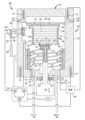
[0019] 図1は、複数の基板135をカセット130に装填するため、第1の位置、例えば上昇位置(すなわち、装填位置)に配置されたカセット130を備えるバッチ処理チャンバ100の概略断面図である。バッチ処理チャンバ100は、内部空間150を囲むチャンバ本体110と、チャンバ本体110の上に配置された蓋111とを有する。チャンバ本体110は、環形状を有するが、他の実施形態では、本体110は、長方形又は任意の閉鎖形状であってもよい。 [0019] Figure 1 is a schematic cross-sectional view of a
[0020] チャンバ本体110は、一又は複数のセクションで製造されてもよい。図1に示す実施形態では、チャンバ本体110は、底壁115、側壁117を含む蓋111を含む。底壁115は、内面151と外面153とを有する。側壁117は、内面155と外面157とを有する。蓋111及びチャンバ本体110は、固定シール118によって共に保持される。冷却チャネル119は、固定シール118に隣接して配置される。他の実施形態(図示せず)では、チャンバ本体110は、上部スプールと、底部115と蓋111との間に配置された下部スプールとを含んでもよい。チャンバ本体110は、一又は複数のHastelloy(登録商標)、Iconel(登録商標)、及びMonel(登録商標)合金などであるが、これらに限定されない、高い耐腐食性を示すニッケルベースの鋼合金から作製されてもよい。 [0020] The
[0021] 一又は複数のカートリッジヒータ112が、チャンバ本体110内に、例えば、底部115又は側壁117の凹部内に配置される。ヒータ112は、チャンバ本体110を能動的に加熱し、チャンバ本体110を290℃よりも高い温度に維持するように構成される。ヒータ112の各々は、抵抗コイル、ランプ、セラミックヒータ、グラファイト系炭素繊維複合材料(CFC)ヒータ、ステンレス鋼ヒータ、又はアルミニウムヒータであってもよい。ヒータ112は、電源105によって給電される。温度センサ114は、チャンバ本体110に連結され、チャンバ本体110の温度を監視するように構成される。ヒータ112への電力は、温度センサ114から受け取ったフィードバックを介してコントローラ180によって制御される。石英のような(少なくともシールドに対して)低い熱伝達係数を有する材料で作られた任意の断熱ライナ116を、チャンバ本体110の側壁117の内面155に沿って内部空間150に配置することができるが、これに限定されるものではない。このような例では、ライナ116は、シェル120と側壁117との間に配置され、シェル120と側壁117との間で伝達される熱量を有利に減少させ、これによって、側壁117の温度調整を補助する。 [0021] One or
[0022] カセット130は、内部空間150内に移動可能に配置される。カセット130は、石英、セラミック、又は他の非熱伝導性材料から製造されうる。カセット130は、その中に複数の基板135を収容し、複数の基板135をバッチ処理チャンバ100に出し入れするのを容易にする。さらに、カセット130は、バッチ処理チャンバ100内の第1の位置とバッチ処理チャンバ100内の第2の位置との間の基板135の移送を容易にし、基板135が高圧及び高温でアニールされるようにする。 [0022]
[0023] カセット130は、上壁132と、底壁134と、側壁136とを含む。カセット130の側壁136は、その内面に形成された複数の基板収納スロット138を有する。各基板収納スロット138は、カセット130の側壁136の内面に沿って垂直に等間隔に配置される。各基板収納スロット138は、複数の基板135のうちの1つをその上に保持するように構成される。一実施例では、カセット130は、基板135を保持するための25個の基板収納スロット138を有することができる。他の実施例では、25個より多い又は少ない基板収納スロット138も想定される。底壁134には、カセット130内への流体の流れを容易にする一又は複数の開口133が形成されている。 [0023]
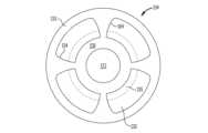
[0024] 図1Cは、カセット130の概略底面図である。一実施形態では、図1Cに示すように、カセット130の底壁134は、中央部分330から環形状の周辺部分131に半径方向に延在する一又は複数のスポーク104を含み、隣接するスポーク104間の開口133を画定する。 [0024] FIG. 1C is a schematic bottom view of
[0025] 図1A及び図1Bに戻ると、プラグ172がカセット130の底壁134に連結される。プラグ172は一又は複数のシール175を含む。シールは、プラグ172の下面に配置することができる。プラグ172は、チャンバ本体110の底壁115を貫通して形成された開口部154の上方に垂直に配置される。プラグ172は、バッチ処理チャンバ100の動作中、カセット130と共に垂直に上下に作動する。いくつかの態様において、図1及び図2に示されるように、開口部154は、内面151に形成され、その中にプラグ172を収容するように構成された階段状の上方プロファイルを含む。作動中、プラグ172は、垂直下方に駆動され、開口部154の階段状プロファイルの底面をシール175と係合させ、それにより、プラグ172と底壁115との間に密閉を形成して、バッチ処理チャンバ100の開口部154を通る流体の流れを阻止する。 [0025] Returning to FIGS.
[0026] プラグが内面151と係合すると、バッチ処理チャンバ100内の上昇した圧力は、バッチ処理チャンバ100の外側の圧力よりも大きく、シール175を内面151と強制的に係合させる。シール175を強制的に係合させることによって、より強く、より流体的に密閉されたシールが形成される。一実施例では、シール175は、パーフルオロエラストマーのような高温ポリマーから作られるが、これに限定されるわけではない。いくつかの実施形態では、シール175はOリングである。いくつかの実施形態では、プラグ172は除外されてもよい。このような実施例では、カセット130の底壁134は底部115に対して密閉する。そのような例では、シール175は、カセット134の底壁134の下面に配置されてもよく、又は任意選択により、シール175を除外してもよいことが企図される。 [0026] When the plug engages the
[0027] プラグ172は、シール175に隣接して内部に配置された冷却チャネル176も含む。冷却チャネル176は、冷却流体源177に流体接続される。限定されるものではないが、不活性流体、誘電性流体、及び高性能伝熱流体などの冷却流体が、冷却チャネル176内で循環されてもよい。冷却チャネル176は、プラグ172及びシール175を冷却して、動作中にシール175を最大完全性温度(maximum integrity temperature)(例えば、約325℃)未満に維持し、それによってシール175の有効寿命を延ばすように構成される。プラグ172は、内部空間150内でプラグ172とカセット130を上下に動かすシャフト174に連結されている。プラグ172は、シャフト174の上端に配置され、シャフト174の別個の構成要素であってもよいし、それと一体的に形成されてもよい。シャフト174の下端は、シャフト174の運動を容易にするアクチュエータ170に連結されている。シャフト174及びアクチュエータ170は、コントローラ180によって制御される。 [0027] The
[0028] バッチ処理チャンバ100はまた、真空リップシール160を含む。真空リップシール160は、外面153とアクチュエータ170との間で、底壁115の外面153に隣接して配置される。真空リップシール160は、シャフト174の周りの真空リップシール160の密閉を容易にするためのシール165を含む。シール165は、パーフルオロエラストマーのような高温ポリマーから作られるが、これに限定されるわけではない。真空リップシール160は、シール175に対するバックアップシール又は冗長シールとして機能する。シール175が故障した場合、内部空間150から流出する加圧流体又は空気は、ポンプ(図示せず)に流体接続された出口169を通って導かれる。低圧動作中、シャフト174がバッチ処理チャンバ100の内部空間150内でカセット130を上下に移動させると、真空リップシール160は、内部空間150からの加圧された処理流体又は空気の漏出、或いは内部空間150内への周囲空気の侵入を防止する。 [0028] The
[0029] いくつかの実施形態では、図1A及び図1Bに示すように、バッチ処理チャンバ100は、熱遮断部178も含む。熱遮断部は、プラグ172の上面及びカセット130の底壁134の下面に隣接して配置される。熱遮断部178は、底壁134に、又はプラグ172の上面に接着されてもよい。熱遮断部178はセラミックから製造されるが、他の材料も想定される。熱遮断部178は、カセット130とシャフト174との間の熱伝達を緩和することによって、カセット130からチャンバの外部への熱の流れを制限するように構成される。 [0029] In some embodiments, the
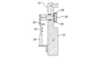
[0030] 図1Dは、バッチ処理チャンバ内に配置された円筒形シェルの部分概略断面図である。円筒形シェル120は、(下降位置にある)カセット130と任意選択の絶縁ライナ116との間に配置される。 [0030] FIG. ID is a partial schematic cross-sectional view of a cylindrical shell positioned within a batch processing chamber.
[0031] シェル120は、その内面106に連結されたヒータ127を有する壁123を含む。シェル120は、壁123内に位置する処理領域125を加熱し、処理領域125内の熱から壁123の外側の外側領域129を遮蔽するように構成される。言い換えるならば、シェル120は、処理領域125と外側領域129との間の熱分離を容易にする。壁123は、高反射性の板金又はHastelloy(登録商標)合金のようなニッケルベースの鋼合金から製造することができる。壁123の外面107は、処理領域125と外側領域129との間の熱分離をさらに容易にするために、任意選択で絶縁層(図示せず)でコーティングされてもよい。 [0031] The
[0032] 壁123の内面106は、複数のフック126を有し、セラミックフックなどがそこに連結されている。複数のフック126は、その上に一又は複数のヒータ127を支持する。ヒータ127は、螺旋状又は軸方向に整列した構成で配置され、アニーリング動作中に処理領域125及びその中に配置された複数の基板135を加熱するように構成される。一実施例では、一又は複数のヒータ127は、処理領域125を550℃の温度まで加熱するように構成される。ヒータは、例えば、ニッケルクロム合金から形成された抵抗ヒータであってもよい。シェル120内のヒータ127は、電源105に電気的に接続される。一実施例では、内面106は熱反射性であり、ヒータ127によって生成された熱を処理領域125に反射させるように構成される。いくつかの態様では、内面1は、熱反射をさらに高めるために、その上に反射コーティングを含むことができる。 [0032] The
[0033] 圧力センサ122は、底部115の内面151上の処理領域125内に配置される。圧力センサ122は、アニーリング処理中に処理領域125の圧力を測定するように構成される。温度センサ124は、圧力センサ122に隣接する底部115の内面151上の処理領域125内に配置され、温度センサ124は、アニーリング処理中に処理領域125の温度を測定するように構成される。 [0033] The
[0034] カセット130の蓋140は、その下面に環状凹部142を含む。環状凹部142は、シェル120の壁123の上に配置されるように構成され、壁123と蓋140との間に間隙128を形成する。一実施例では、蓋140は、環状凹部142を収容するためにシェル120の外径よりも大きい直径を有する。処理流体が処理領域125内に導入されると、間隙128があることによって、残留空気は処理流体によって内部空間150(図1Bに示す)内に押し退けられる。 [0034]
[0035] 図1Dはまた、熱遮断部178の一実施例を示している。図示した実施例では、熱遮断部178は、カプセル化されたカップとして形成されている。カプセル化されたカップは、カセット130の底壁134との接触を最小にする。図1Dに示すように、熱遮断部178は、中空の中央部分109を囲む薄い円筒壁108を有する。中空の中央部分109及び薄い円筒壁は、カセット130とプラグ172との間の熱伝達を低減する。別の実施例では、熱遮断部178は、中空中央部分109を省略しうることが企図される。このような例では、熱遮断部178は、熱絶縁材料から形成することができる。 [0035] FIG. In the illustrated embodiment,
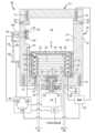
[0036] 図1A及び図1Bに戻り、図1E及び図1Fを参照すると、装填ポート158は、チャンバ本体110の側壁117を通って形成される。図1Eは、開放構成のスリットバルブドア195の概略断面図である。図1Fは、閉鎖構成におけるスリットバルブドア195の概略断面図である。処理中に、複数の基板135をバッチ処理チャンバ100から装填ポート158を通って装填すること又は取り出すことができる。スリットバルブドア195は、装填ポート158を選択的に開閉することによって、装填ポート158を通って内部空間150へアクセスするために使用される。スリットバルブドア195は、装填ポート158を囲む側壁117の内面155と係合するように構成される。シール199は、装填ポート158を覆って密閉することによって、スリットバルブドア195の閉鎖を容易にする。内部空間150内の上昇した圧力は、スリットバルブドア195及びシール199を内面155にさらに係合させる。シール199は、パーフルオロエラストマーのような高温ポリマーから作られるが、これに限定されるものではない。いくつかの実施形態では、シール199はOリングであってもよい。 [0036] Returning to FIGS. 1A and 1B and referring to FIGS. FIG. 1E is a schematic cross-sectional view of
[0037] スリットバルブドア195は、細長いスロット105b内に配置された回転ピン105aを含む。ピン105aは、スリットバルブドア195をバー198aに連結する。バー198aは、水平アクチュエータ194a及び垂直アクチュエータ190に連結されている。水平アクチュエータ194aは、内部空間150内のスリットバルブドア195の一端を、装填ポート158に向かって、また、装填ポート158から離れるように直線的に移動させるように構成される。水平アクチュエータ194aの作動により、スリットバルブドア195はピン105cを中心に枢動し、一方、ピン105aは細長いスロット105b内を移動する。スリットバルブドア195の回転のためのクリアランスを提供するために、第2の水平アクチュエータ194bは、スリットバルブドア195がバー198bを介して内面155から離れる動作を容易にしうる。スリットバルブドア195は、基板の出し入れを可能にするため、非垂直配向(例えば、内面155に対して約45度)に旋回されてもよい。さらなるクリアランスを提供するため、水平アクチュエータ194a、194bは、ブラケット196の作動を容易にするように、リンク192によって垂直アクチュエータ190に連結されるブラケット196に連結されてもよい。ブラケット196の垂直方向の作動は、バー198a、198bを装填ポート158内で垂直方向に移動させることによって、装填ポート158内にさらなるクリアランスを提供する。スリットバルブドア195及び各アクチュエータの運動は、コントローラ180によって制御される。 [0037] The
[0038] バッチ処理チャンバ100内の空気の流れを容易にするために、入口ポート152は、チャンバ本体110の底壁115を貫通して形成され、入口導管259(図2に示す)を内部空間150に流体接続する。出口ポート156はまた、底壁115を貫通して形成され、内部空間150を出口導管361(図3に示す)に接続する。入口ポート152は、一又は複数のガス(例えば、試薬、前駆体、パージガス、又はキャリアガス)を供給するために、ガス供給源に流体連結される。 [0038] To facilitate air flow within the
[0039] 図2は、温度制御された入口流体回路200を概略的に示す。温度制御された入口流体回路200は、入口導管259を介して入口ポート152に流体接続可能である。入口流体回路200は、ガスパネル250と、ソース導管257と、入口導管259に連結された入口分離バルブ255とを含む。一又は複数のヒータ252、254、及び258は、入口流体回路200の異なる部分とインターフェース接続され、入口流体回路200全体にわたる温度制御を容易にする。一又は複数の温度センサ251、253、及び256は、入口流体回路200の異なる部分とインターフェース接続され、温度測定値を取得し、温度測定情報をコントローラ180に提供し、それによってフィードバック制御を容易にする。 [0039] FIG. 2 schematically illustrates a temperature controlled
[0040] 図2に示されているように、ソース導管257はヒータ252とインターフェース接続され、かつ熱連通している。入口分離バルブ255は、ヒータ254とインターフェース接続され、かつ熱連通している。入口導管259は、ヒータ258とインターフェース接続され、かつ熱連通している。温度センサ251は、ソース導管257とインターフェース接続され、ソース導管257の温度を測定するように構成される。温度センサ253は、入口分離バルブ255とインターフェース接続され、入口分離バルブ255の温度を測定するように構成される。温度センサ256は、入口導管259とインターフェース接続され、入口導管259の温度を測定するように構成される。温度読取装置205は、温度センサ251、253及び256から温度測定値を受け取り、表示する。温度読取装置205は、温度情報をコントローラ180に送り、入口流体回路200の温度制御を容易にする。 [0040] As shown in FIG. 2,
[0041] 図3は、温度制御された出口流体回路300を概略的に示す。出口流体回路300は、出口導管361を介して出口ポート156に流体接続可能である。出口流体回路300は、出口分離バルブ365と、排気導管263と、凝集装置(condenser)360と、ポンプ378とを含む。出口流体回路300の熱制御を容易にするために、一又は複数のヒータ362、364、及び366が出口流体回路300の異なる部分とインターフェース接続される。一又は複数の温度センサ367、368、及び369が、出口流体回路300の異なる部分とインターフェース接続され、温度測定値を取得し、温度測定情報をコントローラ180に提供する。図3に示されているように、出口導管361はヒータ362とインターフェース接続され、かつ熱連通している。出口分離バルブ265は、ヒータ364とインターフェース接続され、かつ熱連通している。排気導管363は、ヒータ366とインターフェース接続され、かつ熱連通している。温度センサ367は、出口導管361とインターフェース接続され、出口導管361の温度を測定するように構成される。温度センサ368は、出口分離バルブ365とインターフェース接続され、出口分離バルブ365の温度を測定するように構成される。温度センサ369は、排気導管363とインターフェース接続され、排気導管363の温度を測定するように構成される。温度読取装置305は、温度センサ367、368及び369から温度測定値を受け取り、表示する。温度読取装置305は、出口流体回路300の温度制御を容易にするために、温度情報をコントローラ180に送る。 [0041] FIG. 3 schematically illustrates a temperature controlled
[0042] 凝集装置360は、内部空間150に流体連結され、出口導管361を通って内部空間150を出る処理流体を凝集するように構成される。任意選択的に、凝集装置360を出る凝集した処理流体は、分離バルブ375を経由して熱交換器370を通って送られてもよい。熱交換器370は、処理流体がより容易に管理されうるように、凝集した処理流体をさらに冷却するように構成される。凝集装置360は、凝集導管372によって分離バルブ375に流体接続されている。熱交換器370は、熱交換器導管374によって分離バルブ375に連結される。ポンプ378は、ポンプ導管376によって熱交換器370に流体的に接続され、リサイクル、再利用又は廃棄するため、熱交換器370から容器(図示せず)への液化処理流体のポンピングを容易にする。 [0042] A
[0043] 図2及び図3を参照すると、ヒータ252、254、258、362、364、及び366は、流体回路200及び300を通って流れている処理流体を所定の温度に維持するように構成される。一実施例では、所定の温度は、処理流体の凝結点よりも高い。ヒータ252、254、258、362、364、及び366は、外部環境への熱の損失を防止するために、任意選択により、断熱層で覆われてもよく、それによって、流体入口回路200及び流体出口回路300の温度制御効率が改善される。ヒータ252、254、258、362、364、及び366は、ランプ、抵抗加熱素子、伝熱流体を流すための流体導管、又は他の適切な加熱装置であってもよい。図2及び図3に示すような実施形態では、ヒータ252、254、258、362、364、及び366は、流体回路200及び300の素子の周囲に巻かれた抵抗ヒータである。ヒータ252、254、258、362、364、及び366は、電源105に個別に連結される。いくつかの実施形態では、ヒータ252、254、258、362、364、及び366の各々は、独立して制御されてもよい。温度センサ251、253、256、367、368、及び369は、それぞれ、赤外線センサなどの非接触センサ、又は熱電対などの接触センサになりうる。 [0043] Referring to FIGS. 2 and 3,
[0044] 入口分離バルブ255及び出口分離バルブ365は、遮断バルブである。入口分離バルブ255が開いているときには、ソース導管257を通って流れる処理流体が、内部空間150内で入口導管259及び処理領域125に入るように、出口分離バルブ365は閉じられる。一方、出口分離バルブ365が開いているときには、ガス状生成物が処理領域125から除去され、出口導管361及び排気導管363を通って凝集装置360に流れるように、入口分離バルブ255は閉じられる。 [0044] The
[0045] 処理流体は、バッチ処理チャンバ100内の基板の所望のアニーリングのための処理要件に従って選択されることが企図される。処理流体は、酸素、蒸気、水、過酸化水素、及び/又はアンモニアなどの酸素含有ガス及び/又は窒素含有ガスを含みうる。酸素含有ガス及び/又は窒素含有ガスの代わりに、又はこれに加えて、処理流体は、一又は複数の有機ケイ素化合物、一又は複数のテトラアルキルオルトシリケート、一又は複数のジシロキサン、或いはこれらの任意の組合せなどであるが、これらに限定されないケイ素含有ガスを含有してもよい。いくつかの実施形態では、処理流体は、70barまでの圧力で約550℃の温度の蒸気であってもよい。 [0045] It is contemplated that the processing fluids are selected according to processing requirements for the desired annealing of the substrates within the
[0046] 図1A及び図1Bに戻ると、バッチ処理チャンバは、コントローラ180も含む。コントローラ180は、アクチュエータ170、194a、194b、及び190、並びにバッチ処理チャンバ100の電源105の動作を制御する。また、コントローラ180は、冷却流体源177と、入口流体回路200(図2)と、出口流体回路300(図3)とに接続される。コントローラ180は、圧力センサ122と、温度センサ114及び124とに、通信可能に接続される。コントローラ180は、中央処理装置(CPU)182と、メモリ184と、補助回路186とを含む。CPU182は、産業用の設定で使用されうる任意の形態の汎用コンピュータプロセッサであってよい。メモリ184は、ランダムアクセスメモリ、読取専用メモリ、フロッピー、又はハードディスクドライブ、又は他の形態のデジタル記憶装置であってよい。補助回路186は、通常、CPU182に連結され、キャッシュ、クロック回路、入出力システム、電源などを含みうる。 [0046] Returning to FIGS. 1A and 1B, the batch processing chamber also includes a
[0047] バッチ処理チャンバ100は、70barまでの圧力下、かつ約550℃の温度下で、複数の基板135をアニールするために構成される。動作中、ヒータ112は、バッチ処理チャンバ100を予熱し、その後バッチ処理チャンバ100内に導入される過熱処理流体の凝結を回避するため、290℃を超える温度で内部空間150を維持するように、電源が投入される。 [0047] The
[0048] コントローラは、装填ポート158を開くため、一又は複数のアクチュエータ190、194a、194bを駆動する。装填ポート158の開放と同時に、又は開放した後に、シャフト174はアクチュエータ170によって駆動され、バッチ処理チャンバ100の内部空間150内でカセット130を上昇させる。シャフト174は、ロボットエンドエフェクタ(図示せず)からの複数の基板135をそれぞれの基板収納スロット138上に個別に装填することができるように、各基板収納スロット138を装填ポート158と徐々に整列させる。複数の基板135がカセット130に装填されると、装填ポート158は閉じられる。 [0048] The controller drives one or
[0049] シャフト174は、アクチュエータ170によって駆動され、バッチ処理チャンバ100の内部空間150内でカセット130を下降させる。カセット130が下降位置に下がると、プラグ172が内面151と係合して開口部154を密閉する。同時に、カセット130の蓋140は、シェル120の壁123の上に配置され、これにより、処理領域125を画定する。 [0049]
[0050] シェル120の内部に配置されたヒータ127は、電源105によって電源が投入され、処理領域125及び複数の基板135を約550℃の温度に維持する。過熱状態の処理流体は、ガスパネル250によって、入口流体回路200の入口導管259を通って処理領域125内に導入される。入口導管259を通って流体が導入されている間は、出口流体回路300は作動しない。流体が処理領域125に導入されると、流体に加えられる圧力は徐々に高まる。一実施例では、流体は、約70barの圧力が処理領域125内に確立されるまで、処理領域125内に導入される蒸気である。処理領域内に所望の圧力が確立されると、流体の流れは停止される。 [0050] A
[0051] 複数の基板135は、処理流体に曝される。複数の基板135をアニールするため、高圧かつ高温下で、例えば蒸気に曝される。複数の基板135の処理中、処理領域125、入口導管259及び出口導管361は、処理流体が気相に留まるような温度及び圧力に維持される。例えば、処理領域125、入口導管259及び出口導管361の温度は、加えられた圧力での処理流体の凝結点よりも高い温度に維持される。処理領域125、入口導管259及び出口導管361は、適用される温度で処理ガスの凝縮圧力未満の圧力に維持される。コントローラ180は、温度センサ114及び124、温度読取装置205及び305、並びに圧力センサ122からの情報を使用して、バッチ処理チャンバ100に関して処理流体の流れ、適用される圧力、及び適用される熱を制御する。 [0051] A plurality of
[0052] アニーリング処理が完了すると、出口流体回路300が起動され、処理領域125からの処理流体の除去を容易にする。処理流体は、出口流体回路300の出口導管361を通って処理領域から出る。処理領域125から処理ガスを除去する間は、入口流体回路200は作動しない。処理領域125内の凝縮物の形成を緩和するために、処理領域125から処理流体を除去した後に、ヒータ127の電源はオフにされる。次に、バッチ処理チャンバ100の内部空間150内でカセット130を上昇させるため、シャフト174はアクチュエータ170によって駆動される。次に、装填ポート158は、スリットバルブドア195の駆動を介して開かれ、基板135はバッチ処理チャンバ100から個々に取り出される。 [0052] Once the annealing process is complete,
[0053] 一態様では、バッチ処理チャンバ100は、複数の基板135をカセット130へ装填するときに、或いはカセット130から取り出すときに、0.5気圧未満の圧力で動作する。このような低圧動作の間、真空リップシール160は、シャフト174がカセット130を内部空間150内で上下に移動させるときに有効になる。真空リップシール160は、シャフト174の周囲を密閉することによって、さらに加圧された流体又は空気の内部空間150への漏れを防止する。漏れの軽減を促進するため、真空リップシールは真空ポンプ(図示せず)に連結され、出口169を通って流体又は空気を引き出す。一実施例では、シール175が故障した場合、真空リップシール160は、低圧動作中にバッチ処理チャンバ100の真空完全性を維持できるように、出口169を通る任意の加圧された処理流体の除去を容易にする。 [0053] In one aspect, the
[0054] 本明細書に記載のバッチ処理チャンバは、多くの利点をもたらす。バッチ処理チャンバは、真空下だけでなく高圧下でも動作するように構成される。バッチ処理チャンバは、内面に配置された多数のヒータを有する中空の円筒形シェルを組み込み、アニーリングなどの処理中に複数の基板を550℃まで加熱する。同時に、シェルは、シェル内部の熱がチャンバ壁に伝播するのを防止するための熱シールドとして作用し、チャンバ壁の温度を約290℃から約325℃の範囲に維持することが可能になる。チャンバ壁の温度を約290℃から約325℃の範囲に維持することで、シールが温度劣化することなく、チャンバへのポートを閉じるようにシールを使用することが可能になる。このようなシールを使用しないと、金属シールが必要となる。しかしながら、金属シールは恒久的に設置することが必要で、再利用能力が限られている。さらに、金属シールは、望ましくない粒子汚染を発生させる傾向がある。 [0054] The batch processing chambers described herein provide many advantages. Batch processing chambers are configured to operate not only under vacuum, but also under high pressure. A batch processing chamber incorporates a hollow cylindrical shell with multiple heaters located on its inner surface to heat multiple substrates to 550° C. during processes such as annealing. At the same time, the shell acts as a heat shield to prevent heat inside the shell from propagating to the chamber walls, allowing the temperature of the chamber walls to be maintained in the range of about 290°C to about 325°C. Maintaining the temperature of the chamber walls in the range of about 290° C. to about 325° C. allows the seal to be used to close the port to the chamber without temperature degradation of the seal. Without such seals, metal seals would be required. However, metal seals require permanent installation and have limited reusability. Additionally, metal seals tend to generate undesirable particulate contamination.
[0055] しかも、シールの位置決めによっては、使用圧力により、さらに頑強な密閉を形成することが可能になる。開示されている連結されたプラグ及びスリットバルブドアは共に、このようなシール位置決めが有効であると企図される。 [0055] Moreover, the positioning of the seal allows the working pressure to form a more robust seal. Both the interlocked plug and slit valve doors disclosed are contemplated as being effective in such seal positioning.
[0056] 最終的に、本明細書に開示される入口流体回路及び出口流体回路は、処理流体の温度を、流体回路を流れる処理流体の凝縮点より上に制御し、かつ維持する利点をもたらす。入口流体回路及び出口流体回路の異なる部分に連結された多数のヒータ及び温度センサは、コントローラが入口流体回路、出口流体回路及びチャンバへの熱供給を制御し、かつ維持するのを支援する。本明細書に開示の態様によって提供される追加の温度制御は、処理流体の凝縮を防止し、処理流体を気相に維持し、それによって基板の処理全体を改善する。 [0056] Finally, the inlet and outlet fluid circuits disclosed herein provide the advantage of controlling and maintaining the temperature of the process fluid above the condensation point of the process fluid flowing through the fluid circuit. . Multiple heaters and temperature sensors coupled to different portions of the inlet and outlet fluid circuits assist the controller in controlling and maintaining the heat supply to the inlet and outlet fluid circuits and chambers. The additional temperature control provided by aspects disclosed herein prevents condensation of the process fluid and maintains the process fluid in the vapor phase, thereby improving overall substrate processing.
[0057] 上記は、本開示の特定の実施形態に対象としているが、これらの実施形態は、本開示の原理及び用途の例示にすぎないことを理解されたい。したがって、添付の特許請求の範囲によって定義されるように、本発明の趣旨及び範囲から逸脱することなく、他の実施形態に到達するために、例示的な実施形態に多数の修正を行いうることを理解されたい。
[0057] While the above is directed to specific embodiments of the present disclosure, it should be understood that these embodiments are merely illustrative of the principles and applications of the present disclosure. Accordingly, numerous modifications may be made to the illustrative embodiments to arrive at other embodiments without departing from the spirit and scope of the invention as defined by the appended claims. Please understand.
Claims (15)
Translated fromJapanese前記内部空間内で移動可能に配置されたカセットであって、その内部に複数の基板を装填するために第1の位置まで上昇し、処理のために前記第1の位置の下の第2の位置まで下降するように構成されたカセットと、
前記チャンバ本体に形成された前記開口部を通って配置され、前記カセットに連結されたシャフトと、
前記カセットの底壁に連結されたプラグであって、前記カセットが前記第2の位置にあるときに前記チャンバ本体の前記底壁の上面と係合するように構成された下向きのシールであり、前記開口部及び前記シャフトを包囲し、前記カセットが前記第2の位置にあるときに前記チャンバ本体の前記底壁に対して密閉可能な前記シールを備えるプラグと、
前記チャンバ本体の側壁に配置され、290℃を超える温度に前記チャンバ本体を維持するように動作可能なヒータと、
を備える、バッチ処理チャンバ。a chamber body surrounding an interior space, the chamber body having an opening formed through a bottom wall of the chamber body;
A cassette movably disposed within said interior space, raised to a first position for loading a plurality of substrates therein, and a second position below said first position for processing. a cassette configured to be lowered into position;
a shaft disposed through the opening formed in the chamber body and connected to the cassette;
a plug coupled to the bottom wall of the cassette, the downward facing seal configured to engage an upper surface of the bottom wall of the chamber body when the cassette is in the second position; a plug surrounding the opening and the shaft and comprising the seal sealable against the bottom wall of the chamber body when the cassette is in the second position;
a heater disposed on a sidewall of the chamber body and operable to maintain the chamber body at a temperature greater than 290°C;
A batch processing chamber.
前記内部空間内に移動可能に配置されたカセットであって、第1の位置と前記第1の位置の下の第2の位置との間で移動可能なカセットと、
前記内部空間内に配置され、前記カセットが前記第2の位置にあるときに前記カセットを取り囲む中空の円筒形シェルと、
前記チャンバ本体の側壁に配置され、290℃よりも高い温度に前記チャンバ本体を維持するように動作可能なヒータと、
前記カセットが前記第2の位置にあるときに前記シェルの内面と前記カセットとの間に配置される追加のヒータと、
を備えるバッチ処理チャンバ。a chamber body surrounding an interior space;
a cassette movably disposed within the interior space, the cassette being movable between a first position and a second position below the first position;
a hollow cylindrical shell disposed within the interior space and surrounding the cassette when the cassette is in the second position;
a heater disposed on a sidewall of the chamber body and operable to maintain the chamber body at a temperature greater than 290°C;
an additional heater positioned between the inner surface of the shell and the cassette when the cassette is in the second position;
a batch processing chamber.
前記チャンバ本体の底壁の上面と係合するように構成された下向きのシールを備える、請求項10に記載のバッチ処理チャンバ。further comprising a plug coupled to the bottom wall of the cassette and configured to move up and down within the internal space, the plug comprising:
11. The batch processing chamber of claim 10, comprising a downward facing seal configured to engage an upper surface of the bottom wall of the chamber body.
前記カセットの前記底壁と前記プラグとの間に配置された熱遮断部であって、カプセル化されたカップを備える熱遮断部と、
をさらに備える、請求項11に記載のバッチ処理チャンバ。cooling channels disposed within the plug;
a thermal barrier disposed between the bottom wall of the cassette and the plug, the thermal barrier comprising an encapsulated cup;
12. The batch processing chamber of Claim11 , further comprising:
前記内部空間内に移動可能に配置されたカセットであって、その内部に複数の基板を装填するために第1の位置まで上昇し、処理のために前記第1の位置の下の第2の位置まで下降するように構成されたカセットと、
前記カセットの底壁に連結されたプラグであって、前記カセットが前記第2の位置にあるときに前記チャンバ本体の前記底壁の上面と係合するように構成された下向きシールであり、前記開口部を包囲し、前記カセットが前記第2の位置にあるときに前記チャンバ本体の前記底壁に対して密閉可能な前記シールを備えるプラグと、
前記チャンバ本体の側壁に配置され、290℃よりも高い温度に前記チャンバ本体を維持するように動作可能なヒータと、
前記カセットが前記第2の位置にあるときにシェルの内面と前記カセットとの間に配置される追加のヒータと、
を備える、バッチ処理チャンバ。a chamber body surrounding an interior space, the chamber body having an opening formed through a bottom wall of the chamber body;
A cassette movably disposed within said interior space, raised to a first position for loading a plurality of substrates therein, and a second position below said first position for processing. a cassette configured to be lowered into position;
a plug coupled to the bottom wall of the cassette, the downward facing seal configured to engage an upper surface of the bottom wall of the chamber body when the cassette is in the second position; a plug surrounding the opening and comprising the sealsealable against the bottom wall of the chamber body when the cassette is in the second position;
a heater disposed on a sidewall of the chamber body and operable to maintain the chamber body at a temperature greater than 290°C;
an additional heater positioned between the inner surface of the shell and the cassette when the cassette is in the second position;
A batch processing chamber.
Applications Claiming Priority (3)
| Application Number | Priority Date | Filing Date | Title |
|---|---|---|---|
| US201762586935P | 2017-11-16 | 2017-11-16 | |
| US62/586,935 | 2017-11-16 | ||
| PCT/US2018/055401WO2019099125A1 (en) | 2017-11-16 | 2018-10-11 | High pressure steam anneal processing apparatus |
Publications (2)
| Publication Number | Publication Date |
|---|---|
| JP2021503716A JP2021503716A (en) | 2021-02-12 |
| JP7330181B2true JP7330181B2 (en) | 2023-08-21 |
Family
ID=66433522
Family Applications (1)
| Application Number | Title | Priority Date | Filing Date |
|---|---|---|---|
| JP2020526392AActiveJP7330181B2 (en) | 2017-11-16 | 2018-10-11 | High-pressure steam annealing treatment equipment |
Country Status (7)
| Country | Link |
|---|---|
| US (1) | US10854483B2 (en) |
| JP (1) | JP7330181B2 (en) |
| KR (1) | KR102622303B1 (en) |
| CN (1) | CN111373519B (en) |
| SG (1) | SG11202003438QA (en) |
| TW (2) | TWI700748B (en) |
| WO (1) | WO2019099125A1 (en) |
Families Citing this family (20)
| Publication number | Priority date | Publication date | Assignee | Title |
|---|---|---|---|---|
| US10224224B2 (en) | 2017-03-10 | 2019-03-05 | Micromaterials, LLC | High pressure wafer processing systems and related methods |
| US10622214B2 (en) | 2017-05-25 | 2020-04-14 | Applied Materials, Inc. | Tungsten defluorination by high pressure treatment |
| WO2019036157A1 (en) | 2017-08-18 | 2019-02-21 | Applied Materials, Inc. | High pressure and high temperature anneal chamber |
| US10276411B2 (en) | 2017-08-18 | 2019-04-30 | Applied Materials, Inc. | High pressure and high temperature anneal chamber |
| JP7274461B2 (en) | 2017-09-12 | 2023-05-16 | アプライド マテリアルズ インコーポレイテッド | Apparatus and method for manufacturing semiconductor structures using protective barrier layers |
| CN117936420A (en) | 2017-11-11 | 2024-04-26 | 微材料有限责任公司 | Gas delivery system for high pressure processing chamber |
| KR20200075892A (en) | 2017-11-17 | 2020-06-26 | 어플라이드 머티어리얼스, 인코포레이티드 | Condenser system for high pressure treatment systems |
| SG11202008256WA (en) | 2018-03-09 | 2020-09-29 | Applied Materials Inc | High pressure annealing process for metal containing materials |
| US10714331B2 (en) | 2018-04-04 | 2020-07-14 | Applied Materials, Inc. | Method to fabricate thermally stable low K-FinFET spacer |
| US10950429B2 (en) | 2018-05-08 | 2021-03-16 | Applied Materials, Inc. | Methods of forming amorphous carbon hard mask layers and hard mask layers formed therefrom |
| US10748783B2 (en) | 2018-07-25 | 2020-08-18 | Applied Materials, Inc. | Gas delivery module |
| US10675581B2 (en) | 2018-08-06 | 2020-06-09 | Applied Materials, Inc. | Gas abatement apparatus |
| CN112640065B (en) | 2018-10-30 | 2024-10-01 | 应用材料公司 | Method for etching structures for semiconductor applications |
| WO2020101935A1 (en) | 2018-11-16 | 2020-05-22 | Applied Materials, Inc. | Film deposition using enhanced diffusion process |
| WO2020117462A1 (en) | 2018-12-07 | 2020-06-11 | Applied Materials, Inc. | Semiconductor processing system |
| US11901222B2 (en) | 2020-02-17 | 2024-02-13 | Applied Materials, Inc. | Multi-step process for flowable gap-fill film |
| US11415230B2 (en)* | 2020-03-31 | 2022-08-16 | Applied Material, Inc. | Slit valve pneumatic control |
| US12002668B2 (en)* | 2021-06-25 | 2024-06-04 | Applied Materials, Inc. | Thermal management hardware for uniform temperature control for enhanced bake-out for cluster tool |
| JP7465855B2 (en)* | 2021-09-27 | 2024-04-11 | 芝浦メカトロニクス株式会社 | Heat treatment device, loading/unloading tool, and method for forming organic film |
| CN117542767B (en)* | 2024-01-10 | 2024-03-26 | 合肥费舍罗热工装备有限公司 | Vertical semiconductor welding furnace |
Citations (4)
| Publication number | Priority date | Publication date | Assignee | Title |
|---|---|---|---|---|
| JP2001512789A (en) | 1997-08-11 | 2001-08-28 | トーレックス・イクイップメント・コーポレーション | Mini-batch process chamber |
| JP2005533378A (en) | 2002-07-15 | 2005-11-04 | アヴィザ テクノロジー インコーポレイテッド | Heat treatment apparatus and configurable vertical chamber |
| JP2015530477A (en) | 2012-06-27 | 2015-10-15 | イノシティ カンパニー リミテッド | Substrate heating apparatus and process chamber |
| JP2017120883A (en) | 2015-12-28 | 2017-07-06 | ユ−ジーン テクノロジー カンパニー.リミテッド | Substrate processing device |
Family Cites Families (300)
| Publication number | Priority date | Publication date | Assignee | Title |
|---|---|---|---|---|
| US4524587A (en) | 1967-01-10 | 1985-06-25 | Kantor Frederick W | Rotary thermodynamic apparatus and method |
| JPS4820850B1 (en)* | 1970-11-21 | 1973-06-25 | ||
| JPS634616A (en) | 1986-06-25 | 1988-01-09 | Hitachi Tokyo Electron Co Ltd | Steam treating unit |
| JPH0748489B2 (en) | 1987-07-27 | 1995-05-24 | 富士通株式会社 | Plasma processing device |
| US4879259A (en) | 1987-09-28 | 1989-11-07 | The Board Of Trustees Of The Leland Stanford Junion University | Rapid thermal annealing of gallium arsenide with trimethyl arsenic overpressure |
| US5092728A (en)* | 1987-10-15 | 1992-03-03 | Epsilon Technology, Inc. | Substrate loading apparatus for a CVD process |
| US5114513A (en) | 1988-10-27 | 1992-05-19 | Omron Tateisi Electronics Co. | Optical device and manufacturing method thereof |
| JP2730695B2 (en) | 1989-04-10 | 1998-03-25 | 忠弘 大見 | Tungsten film forming equipment |
| US5126117A (en) | 1990-05-22 | 1992-06-30 | Custom Engineered Materials, Inc. | Device for preventing accidental releases of hazardous gases |
| US5175123A (en) | 1990-11-13 | 1992-12-29 | Motorola, Inc. | High-pressure polysilicon encapsulated localized oxidation of silicon |
| US5050540A (en) | 1991-01-29 | 1991-09-24 | Arne Lindberg | Method of gas blanketing a boiler |
| JPH05129296A (en) | 1991-11-05 | 1993-05-25 | Fujitsu Ltd | Method of flatting conductive film |
| JP3230836B2 (en)* | 1992-04-09 | 2001-11-19 | 東京エレクトロン株式会社 | Heat treatment equipment |
| US5319212A (en) | 1992-10-07 | 1994-06-07 | Genus, Inc. | Method of monitoring ion beam current in ion implantation apparatus for use in manufacturing semiconductors |
| JPH06283496A (en) | 1993-03-26 | 1994-10-07 | Dainippon Screen Mfg Co Ltd | Dryer of substrate after washing |
| US5607002A (en) | 1993-04-28 | 1997-03-04 | Advanced Delivery & Chemical Systems, Inc. | Chemical refill system for high purity chemicals |
| US5578132A (en) | 1993-07-07 | 1996-11-26 | Tokyo Electron Kabushiki Kaisha | Apparatus for heat treating semiconductors at normal pressure and low pressure |
| US5880041A (en) | 1994-05-27 | 1999-03-09 | Motorola Inc. | Method for forming a dielectric layer using high pressure |
| US5808245A (en) | 1995-01-03 | 1998-09-15 | Donaldson Company, Inc. | Vertical mount catalytic converter muffler |
| US5620524A (en) | 1995-02-27 | 1997-04-15 | Fan; Chiko | Apparatus for fluid delivery in chemical vapor deposition systems |
| KR100251341B1 (en) | 1995-05-08 | 2000-05-01 | 오카노 사다오 | Manufacturing method of optical waveguide |
| JP2872637B2 (en) | 1995-07-10 | 1999-03-17 | アプライド マテリアルズ インコーポレイテッド | Microwave plasma based applicator |
| US5895274A (en) | 1996-01-22 | 1999-04-20 | Micron Technology, Inc. | High-pressure anneal process for integrated circuits |
| KR980012044A (en) | 1996-03-01 | 1998-04-30 | 히가시 데츠로 | Substrate drying apparatus and substrate drying method |
| US5998305A (en) | 1996-03-29 | 1999-12-07 | Praxair Technology, Inc. | Removal of carbon from substrate surfaces |
| US5738915A (en) | 1996-09-19 | 1998-04-14 | Lambda Technologies, Inc. | Curing polymer layers on semiconductor substrates using variable frequency microwave energy |
| US6444037B1 (en) | 1996-11-13 | 2002-09-03 | Applied Materials, Inc. | Chamber liner for high temperature processing chamber |
| US6082950A (en) | 1996-11-18 | 2000-07-04 | Applied Materials, Inc. | Front end wafer staging with wafer cassette turntables and on-the-fly wafer center finding |
| US5730885A (en)* | 1996-12-03 | 1998-03-24 | Union Carbide Chemicals & Plastics Technology Corporation | Screen packs for reducing gels in polypropylene copolymers |
| US5846073A (en)* | 1997-03-07 | 1998-12-08 | Semitool, Inc. | Semiconductor furnace processing vessel base |
| US6136664A (en) | 1997-08-07 | 2000-10-24 | International Business Machines Corporation | Filling of high aspect ratio trench isolation |
| US20030049372A1 (en) | 1997-08-11 | 2003-03-13 | Cook Robert C. | High rate deposition at low pressures in a small batch reactor |
| US5963817A (en) | 1997-10-16 | 1999-10-05 | International Business Machines Corporation | Bulk and strained silicon on insulator using local selective oxidation |
| JP3199006B2 (en) | 1997-11-18 | 2001-08-13 | 日本電気株式会社 | Method of forming interlayer insulating film and insulating film forming apparatus |
| US6442980B2 (en) | 1997-11-26 | 2002-09-03 | Chart Inc. | Carbon dioxide dry cleaning system |
| US6846739B1 (en) | 1998-02-27 | 2005-01-25 | Micron Technology, Inc. | MOCVD process using ozone as a reactant to deposit a metal oxide barrier layer |
| US6164412A (en) | 1998-04-03 | 2000-12-26 | Arvin Industries, Inc. | Muffler |
| US6719516B2 (en) | 1998-09-28 | 2004-04-13 | Applied Materials, Inc. | Single wafer load lock with internal wafer transport |
| US20030101938A1 (en) | 1998-10-27 | 2003-06-05 | Applied Materials, Inc. | Apparatus for the deposition of high dielectric constant films |
| TW517092B (en)* | 1999-03-17 | 2003-01-11 | Kobe Steel Ltd | High-temperature and high-pressure treatment device |
| US6468490B1 (en) | 2000-06-29 | 2002-10-22 | Applied Materials, Inc. | Abatement of fluorine gas from effluent |
| US6612317B2 (en) | 2000-04-18 | 2003-09-02 | S.C. Fluids, Inc | Supercritical fluid delivery and recovery system for semiconductor wafer processing |
| US6334266B1 (en) | 1999-09-20 | 2002-01-01 | S.C. Fluids, Inc. | Supercritical fluid drying system and method of use |
| EP1077477B1 (en) | 1999-08-17 | 2008-12-17 | Applied Materials, Inc. | Surface treatment of C-doped SiO2 film to enhance film stability during O2 ashing |
| US6299753B1 (en) | 1999-09-01 | 2001-10-09 | Applied Materials, Inc. | Double pressure vessel chemical dispenser unit |
| JP2001110729A (en) | 1999-10-06 | 2001-04-20 | Mitsubishi Heavy Ind Ltd | Apparratus for continuously manufacturing method of semiconductor element |
| US20030148631A1 (en) | 1999-11-08 | 2003-08-07 | Taiwan Semiconductor Manufacturing Company | Oxidative annealing method for forming etched spin-on-glass (SOG) planarizing layer with uniform etch profile |
| US6500603B1 (en) | 1999-11-11 | 2002-12-31 | Mitsui Chemicals, Inc. | Method for manufacturing polymer optical waveguide |
| US6150286A (en) | 2000-01-03 | 2000-11-21 | Advanced Micro Devices, Inc. | Method of making an ultra thin silicon nitride film |
| US6541367B1 (en) | 2000-01-18 | 2003-04-01 | Applied Materials, Inc. | Very low dielectric constant plasma-enhanced CVD films |
| US6319766B1 (en) | 2000-02-22 | 2001-11-20 | Applied Materials, Inc. | Method of tantalum nitride deposition by tantalum oxide densification |
| JP2001250787A (en) | 2000-03-06 | 2001-09-14 | Hitachi Kokusai Electric Inc | Substrate processing apparatus and substrate processing method |
| US20040025908A1 (en) | 2000-04-18 | 2004-02-12 | Stephen Douglas | Supercritical fluid delivery system for semiconductor wafer processing |
| JP3497450B2 (en)* | 2000-07-06 | 2004-02-16 | 東京エレクトロン株式会社 | Batch heat treatment apparatus and control method thereof |
| US7166524B2 (en) | 2000-08-11 | 2007-01-23 | Applied Materials, Inc. | Method for ion implanting insulator material to reduce dielectric constant |
| JP4342745B2 (en)* | 2000-09-27 | 2009-10-14 | 株式会社日立国際電気 | Substrate processing method and semiconductor device manufacturing method |
| US6852167B2 (en) | 2001-03-01 | 2005-02-08 | Micron Technology, Inc. | Methods, systems, and apparatus for uniform chemical-vapor depositions |
| US6797336B2 (en) | 2001-03-22 | 2004-09-28 | Ambp Tech Corporation | Multi-component substances and processes for preparation thereof |
| JP4335469B2 (en) | 2001-03-22 | 2009-09-30 | 株式会社荏原製作所 | Method and apparatus for adjusting gas circulation rate of vacuum exhaust device |
| JP4015818B2 (en)* | 2001-03-28 | 2007-11-28 | 株式会社日立国際電気 | Semiconductor manufacturing equipment |
| TW544797B (en) | 2001-04-17 | 2003-08-01 | Kobe Steel Ltd | High-pressure processing apparatus |
| JP2002319571A (en) | 2001-04-20 | 2002-10-31 | Kawasaki Microelectronics Kk | Preprocessing method for etching tank and manufacturing method for semiconductor device |
| US7080651B2 (en) | 2001-05-17 | 2006-07-25 | Dainippon Screen Mfg. Co., Ltd. | High pressure processing apparatus and method |
| EP1271636A1 (en) | 2001-06-22 | 2003-01-02 | Infineon Technologies AG | Thermal oxidation process control by controlling oxidation agent partial pressure |
| JP2003051474A (en) | 2001-08-03 | 2003-02-21 | Kobe Steel Ltd | High-pressure processing apparatus |
| US6781801B2 (en) | 2001-08-10 | 2004-08-24 | Seagate Technology Llc | Tunneling magnetoresistive sensor with spin polarized current injection |
| US6531412B2 (en) | 2001-08-10 | 2003-03-11 | International Business Machines Corporation | Method for low temperature chemical vapor deposition of low-k films using selected cyclosiloxane and ozone gases for semiconductor applications |
| US6619304B2 (en) | 2001-09-13 | 2003-09-16 | Micell Technologies, Inc. | Pressure chamber assembly including non-mechanical drive means |
| US20030098069A1 (en) | 2001-11-26 | 2003-05-29 | Sund Wesley E. | High purity fluid delivery system |
| KR100450564B1 (en) | 2001-12-20 | 2004-09-30 | 동부전자 주식회사 | Post treatment method for metal line of semiconductor device |
| US6848458B1 (en) | 2002-02-05 | 2005-02-01 | Novellus Systems, Inc. | Apparatus and methods for processing semiconductor substrates using supercritical fluids |
| US6632325B2 (en) | 2002-02-07 | 2003-10-14 | Applied Materials, Inc. | Article for use in a semiconductor processing chamber and method of fabricating same |
| US7589029B2 (en) | 2002-05-02 | 2009-09-15 | Micron Technology, Inc. | Atomic layer deposition and conversion |
| US7638727B2 (en) | 2002-05-08 | 2009-12-29 | Btu International Inc. | Plasma-assisted heat treatment |
| US7521089B2 (en) | 2002-06-13 | 2009-04-21 | Tokyo Electron Limited | Method and apparatus for controlling the movement of CVD reaction byproduct gases to adjacent process chambers |
| US20070243317A1 (en)* | 2002-07-15 | 2007-10-18 | Du Bois Dale R | Thermal Processing System and Configurable Vertical Chamber |
| US20070212850A1 (en) | 2002-09-19 | 2007-09-13 | Applied Materials, Inc. | Gap-fill depositions in the formation of silicon containing dielectric materials |
| US7335609B2 (en) | 2004-08-27 | 2008-02-26 | Applied Materials, Inc. | Gap-fill depositions introducing hydroxyl-containing precursors in the formation of silicon containing dielectric materials |
| JP2004127958A (en) | 2002-09-30 | 2004-04-22 | Kyoshin Engineering:Kk | Apparatus and method for performing high pressure anneal steam treatment |
| US20040060519A1 (en) | 2002-10-01 | 2004-04-01 | Seh America Inc. | Quartz to quartz seal using expanded PTFE gasket material |
| US6889508B2 (en) | 2002-10-02 | 2005-05-10 | The Boc Group, Inc. | High pressure CO2 purification and supply system |
| US7270761B2 (en) | 2002-10-18 | 2007-09-18 | Appleid Materials, Inc | Fluorine free integrated process for etching aluminum including chamber dry clean |
| US20040112409A1 (en) | 2002-12-16 | 2004-06-17 | Supercritical Sysems, Inc. | Fluoride in supercritical fluid for photoresist and residue removal |
| EP1597752A2 (en) | 2003-02-04 | 2005-11-23 | Applied Materials, Inc. | Tailoring nitrogen profile in silicon oxynitride using rapid thermal annealing with ammonia under ultra-low pressure |
| JPWO2004075272A1 (en)* | 2003-02-21 | 2006-06-01 | 株式会社日立国際電気 | Substrate processing apparatus and semiconductor device manufacturing method |
| JP3956049B2 (en) | 2003-03-07 | 2007-08-08 | 東京エレクトロン株式会社 | Method for forming tungsten film |
| US6939794B2 (en) | 2003-06-17 | 2005-09-06 | Micron Technology, Inc. | Boron-doped amorphous carbon film for use as a hard etch mask during the formation of a semiconductor device |
| US20070012402A1 (en) | 2003-07-08 | 2007-01-18 | Sundew Technologies, Llc | Apparatus and method for downstream pressure control and sub-atmospheric reactive gas abatement |
| JP4173781B2 (en) | 2003-08-13 | 2008-10-29 | 株式会社神戸製鋼所 | High pressure processing method |
| WO2005057663A2 (en) | 2003-12-10 | 2005-06-23 | Koninklijke Philips Electronics N.V. | Method and apparatus for fabrication of metal-oxide semiconductor integrated circuit devices |
| US7158221B2 (en) | 2003-12-23 | 2007-01-02 | Applied Materials, Inc. | Method and apparatus for performing limited area spectral analysis |
| US20050136684A1 (en) | 2003-12-23 | 2005-06-23 | Applied Materials, Inc. | Gap-fill techniques |
| US20050250347A1 (en) | 2003-12-31 | 2005-11-10 | Bailey Christopher M | Method and apparatus for maintaining by-product volatility in deposition process |
| US7030468B2 (en) | 2004-01-16 | 2006-04-18 | International Business Machines Corporation | Low k and ultra low k SiCOH dielectric films and methods to form the same |
| US7128570B2 (en)* | 2004-01-21 | 2006-10-31 | Asm International N.V. | Method and apparatus for purging seals in a thermal reactor |
| US20050187647A1 (en) | 2004-02-19 | 2005-08-25 | Kuo-Hua Wang | Intelligent full automation controlled flow for a semiconductor furnace tool |
| JP4393268B2 (en) | 2004-05-20 | 2010-01-06 | 株式会社神戸製鋼所 | Drying method of fine structure |
| US20050269291A1 (en) | 2004-06-04 | 2005-12-08 | Tokyo Electron Limited | Method of operating a processing system for treating a substrate |
| US7521378B2 (en) | 2004-07-01 | 2009-04-21 | Micron Technology, Inc. | Low temperature process for polysilazane oxidation/densification |
| US7491658B2 (en) | 2004-10-13 | 2009-02-17 | International Business Machines Corporation | Ultra low k plasma enhanced chemical vapor deposition processes using a single bifunctional precursor containing both a SiCOH matrix functionality and organic porogen functionality |
| US7427571B2 (en) | 2004-10-15 | 2008-09-23 | Asm International, N.V. | Reactor design for reduced particulate generation |
| JP2008521261A (en) | 2004-11-22 | 2008-06-19 | アプライド マテリアルズ インコーポレイテッド | Substrate processing apparatus using batch processing chamber |
| KR100697280B1 (en) | 2005-02-07 | 2007-03-20 | 삼성전자주식회사 | Pressure regulating method of semiconductor manufacturing equipment |
| JP4475136B2 (en)* | 2005-02-18 | 2010-06-09 | 東京エレクトロン株式会社 | Processing system, pre-processing apparatus and storage medium |
| CN101128622B (en) | 2005-02-22 | 2010-08-25 | 埃克提斯公司 | Etching chamber with subchamber |
| US7211525B1 (en) | 2005-03-16 | 2007-05-01 | Novellus Systems, Inc. | Hydrogen treatment enhanced gap fill |
| WO2006101315A1 (en) | 2005-03-21 | 2006-09-28 | Pkl Co., Ltd. | Device and method for cleaning photomask |
| US20060226117A1 (en) | 2005-03-29 | 2006-10-12 | Bertram Ronald T | Phase change based heating element system and method |
| US7351057B2 (en)* | 2005-04-27 | 2008-04-01 | Asm International N.V. | Door plate for furnace |
| US20120060868A1 (en) | 2005-06-07 | 2012-03-15 | Donald Gray | Microscale fluid delivery system |
| JP5276436B2 (en) | 2005-06-10 | 2013-08-28 | オブデュキャット、アクチボラグ | Pattern duplication with intermediate stamp |
| JP4747693B2 (en) | 2005-06-28 | 2011-08-17 | 住友電気工業株式会社 | Method for forming resin body, method for forming structure for optical waveguide, and method for forming optical component |
| US7361231B2 (en) | 2005-07-01 | 2008-04-22 | Ekc Technology, Inc. | System and method for mid-pressure dense phase gas and ultrasonic cleaning |
| WO2007018016A1 (en) | 2005-08-05 | 2007-02-15 | Hitachi Kokusai Electric Inc. | Substrate processing equipment, cooling gas supply nozzle and method for fabricating semiconductor device |
| US7534080B2 (en) | 2005-08-26 | 2009-05-19 | Ascentool, Inc. | Vacuum processing and transfer system |
| US7531404B2 (en) | 2005-08-30 | 2009-05-12 | Intel Corporation | Semiconductor device having a metal gate electrode formed on an annealed high-k gate dielectric layer |
| KR100696178B1 (en) | 2005-09-13 | 2007-03-20 | 한국전자통신연구원 | Optical waveguide master and its manufacturing method |
| US8926731B2 (en) | 2005-09-13 | 2015-01-06 | Rasirc | Methods and devices for producing high purity steam |
| US20080257260A9 (en)* | 2005-09-30 | 2008-10-23 | Applied Materials, Inc. | Batch wafer handling system |
| WO2007043383A1 (en) | 2005-10-07 | 2007-04-19 | Nikon Corporation | Fine structure body and method for manufacturing same |
| US7387968B2 (en) | 2005-11-08 | 2008-06-17 | Tokyo Electron Limited | Batch photoresist dry strip and ash system and process |
| US8306026B2 (en) | 2005-12-15 | 2012-11-06 | Toshiba America Research, Inc. | Last hop topology sensitive multicasting key management |
| US20070187386A1 (en) | 2006-02-10 | 2007-08-16 | Poongsan Microtec Corporation | Methods and apparatuses for high pressure gas annealing |
| US7578258B2 (en) | 2006-03-03 | 2009-08-25 | Lam Research Corporation | Methods and apparatus for selective pre-coating of a plasma processing chamber |
| JP2007242791A (en) | 2006-03-07 | 2007-09-20 | Hitachi Kokusai Electric Inc | Substrate processing equipment |
| WO2007133595A2 (en) | 2006-05-08 | 2007-11-22 | The Board Of Trustees Of The University Of Illinois | Integrated vacuum absorption steam cycle gas separation |
| US7825038B2 (en) | 2006-05-30 | 2010-11-02 | Applied Materials, Inc. | Chemical vapor deposition of high quality flow-like silicon dioxide using a silicon containing precursor and atomic oxygen |
| US7650965B2 (en) | 2006-06-09 | 2010-01-26 | Emcon Technologies Llc | Exhaust system |
| US7371998B2 (en)* | 2006-07-05 | 2008-05-13 | Semitool, Inc. | Thermal wafer processor |
| JP2008073611A (en) | 2006-09-21 | 2008-04-03 | Dainippon Screen Mfg Co Ltd | High pressure treating device |
| JP4814038B2 (en) | 2006-09-25 | 2011-11-09 | 株式会社日立国際電気 | Substrate processing apparatus and method for attaching / detaching reaction vessel |
| US7790587B2 (en) | 2006-11-07 | 2010-09-07 | Intel Corporation | Method to reduce junction leakage through partial regrowth with ultrafast anneal and structures formed thereby |
| US20080169183A1 (en) | 2007-01-16 | 2008-07-17 | Varian Semiconductor Equipment Associates, Inc. | Plasma Source with Liner for Reducing Metal Contamination |
| JP2008192642A (en) | 2007-01-31 | 2008-08-21 | Tokyo Electron Ltd | Substrate processing apparatus |
| US20080233404A1 (en) | 2007-03-22 | 2008-09-25 | 3M Innovative Properties Company | Microreplication tools and patterns using laser induced thermal embossing |
| JP5135856B2 (en) | 2007-03-31 | 2013-02-06 | 東京エレクトロン株式会社 | Trap device, exhaust system and treatment system using the same |
| DE102007017641A1 (en) | 2007-04-13 | 2008-10-16 | Infineon Technologies Ag | Curing of layers on the semiconductor module by means of electromagnetic fields |
| KR101560705B1 (en) | 2007-05-25 | 2015-10-16 | 어플라이드 머티어리얼스, 인코포레이티드 | Methods and apparatus for assembling and operating electronic device manufacturing systems |
| WO2008156687A1 (en) | 2007-06-15 | 2008-12-24 | Applied Materials, Inc. | Methods and systems for designing and validating operation of abatement systems |
| US20090004405A1 (en)* | 2007-06-29 | 2009-01-01 | Applied Materials, Inc. | Thermal Batch Reactor with Removable Susceptors |
| KR101442238B1 (en) | 2007-07-26 | 2014-09-23 | 주식회사 풍산마이크로텍 | Method for manufacturing semiconductor device by high pressure oxygen heat treatment |
| JP4470970B2 (en)* | 2007-07-31 | 2010-06-02 | 東京エレクトロン株式会社 | Plasma processing equipment |
| US7951728B2 (en) | 2007-09-24 | 2011-05-31 | Applied Materials, Inc. | Method of improving oxide growth rate of selective oxidation processes |
| US7541297B2 (en) | 2007-10-22 | 2009-06-02 | Applied Materials, Inc. | Method and system for improving dielectric film quality for void free gap fill |
| US7803722B2 (en) | 2007-10-22 | 2010-09-28 | Applied Materials, Inc | Methods for forming a dielectric layer within trenches |
| US7867923B2 (en) | 2007-10-22 | 2011-01-11 | Applied Materials, Inc. | High quality silicon oxide films by remote plasma CVD from disilane precursors |
| WO2009055750A1 (en) | 2007-10-26 | 2009-04-30 | Applied Materials, Inc. | Methods and apparatus for smart abatement using an improved fuel circuit |
| JP5299605B2 (en) | 2007-11-19 | 2013-09-25 | 日揮触媒化成株式会社 | Method for repairing damage of low dielectric constant silica-based coating and low dielectric constant silica-based coating repaired by the method |
| US7651959B2 (en) | 2007-12-03 | 2010-01-26 | Asm Japan K.K. | Method for forming silazane-based dielectric film |
| KR20090064279A (en) | 2007-12-14 | 2009-06-18 | 노벨러스 시스템즈, 인코포레이티드 | Protective layer for damage-free gap filling |
| US7776740B2 (en) | 2008-01-22 | 2010-08-17 | Tokyo Electron Limited | Method for integrating selective low-temperature ruthenium deposition into copper metallization of a semiconductor device |
| JP4815464B2 (en) | 2008-03-31 | 2011-11-16 | 株式会社日立製作所 | Fine structure transfer stamper and fine structure transfer apparatus |
| US7655532B1 (en) | 2008-07-25 | 2010-02-02 | Taiwan Semiconductor Manufacturing Company, Ltd. | STI film property using SOD post-treatment |
| JP2010056541A (en) | 2008-07-31 | 2010-03-11 | Semiconductor Energy Lab Co Ltd | Semiconductor device and manufacturing method thereof |
| US20100089315A1 (en) | 2008-09-22 | 2010-04-15 | Applied Materials, Inc. | Shutter disk for physical vapor deposition chamber |
| US8153533B2 (en) | 2008-09-24 | 2012-04-10 | Lam Research | Methods and systems for preventing feature collapse during microelectronic topography fabrication |
| KR20100035000A (en) | 2008-09-25 | 2010-04-02 | 삼성전자주식회사 | Semiconductor device having isolation layer with isolation trench of different aspect ratio and isolation trench gap fill method of fabricating the same |
| US7891228B2 (en) | 2008-11-18 | 2011-02-22 | Mks Instruments, Inc. | Dual-mode mass flow verification and mass flow delivery system and method |
| US8557712B1 (en) | 2008-12-15 | 2013-10-15 | Novellus Systems, Inc. | PECVD flowable dielectric gap fill |
| JP2010205854A (en) | 2009-03-02 | 2010-09-16 | Fujitsu Semiconductor Ltd | Method of manufacturing semiconductor device |
| US20100304027A1 (en) | 2009-05-27 | 2010-12-02 | Applied Materials, Inc. | Substrate processing system and methods thereof |
| JP4415062B1 (en) | 2009-06-22 | 2010-02-17 | 富士フイルム株式会社 | THIN FILM TRANSISTOR AND METHOD FOR PRODUCING THIN FILM TRANSISTOR |
| KR20110000960A (en) | 2009-06-29 | 2011-01-06 | 삼성전자주식회사 | Semiconductor chip, stack module, memory card and manufacturing method thereof |
| US8741788B2 (en) | 2009-08-06 | 2014-06-03 | Applied Materials, Inc. | Formation of silicon oxide using non-carbon flowable CVD processes |
| JP2011066100A (en) | 2009-09-16 | 2011-03-31 | Bridgestone Corp | Photocurable transfer sheet and method for forming recessed and projected pattern using same |
| US8449942B2 (en) | 2009-11-12 | 2013-05-28 | Applied Materials, Inc. | Methods of curing non-carbon flowable CVD films |
| KR101370301B1 (en) | 2009-11-20 | 2014-03-05 | 가부시키가이샤 한도오따이 에네루기 켄큐쇼 | Method for manufacturing semiconductor device |
| US20110151677A1 (en) | 2009-12-21 | 2011-06-23 | Applied Materials, Inc. | Wet oxidation process performed on a dielectric material formed from a flowable cvd process |
| SG182336A1 (en) | 2010-01-06 | 2012-08-30 | Applied Materials Inc | Flowable dielectric using oxide liner |
| KR101837648B1 (en) | 2010-01-07 | 2018-04-19 | 어플라이드 머티어리얼스, 인코포레이티드 | Insitu ozone cure for radicalcomponent cvd |
| KR101775608B1 (en) | 2010-01-21 | 2017-09-19 | 파워다인, 인코포레이티드 | Generating steam from carbonaceous material |
| US8293658B2 (en) | 2010-02-17 | 2012-10-23 | Asm America, Inc. | Reactive site deactivation against vapor deposition |
| JP2013521650A (en) | 2010-03-05 | 2013-06-10 | アプライド マテリアルズ インコーポレイテッド | Conformal layer by radical component CVD |
| KR101163711B1 (en) | 2010-06-15 | 2012-07-09 | 서울대학교산학협력단 | 1t dram device having two gates on recessed body and method of operating and fabricating the same |
| CN101871043B (en) | 2010-06-25 | 2012-07-18 | 东莞市康汇聚线材科技有限公司 | Annealing furnace steam generator and control method thereof |
| US8318584B2 (en) | 2010-07-30 | 2012-11-27 | Applied Materials, Inc. | Oxide-rich liner layer for flowable CVD gapfill |
| JP2012049446A (en) | 2010-08-30 | 2012-03-08 | Toshiba Corp | Supercritical drying method and supercritical drying system |
| EP2426720A1 (en) | 2010-09-03 | 2012-03-07 | Applied Materials, Inc. | Staggered thin film transistor and method of forming the same |
| TW201216331A (en) | 2010-10-05 | 2012-04-16 | Applied Materials Inc | Ultra high selectivity doped amorphous carbon strippable hardmask development and integration |
| JP5806827B2 (en)* | 2011-03-18 | 2015-11-10 | 東京エレクトロン株式会社 | Gate valve apparatus, substrate processing apparatus and substrate processing method thereof |
| JP5450494B2 (en) | 2011-03-25 | 2014-03-26 | 株式会社東芝 | Supercritical drying method for semiconductor substrates |
| KR20140027917A (en) | 2011-03-25 | 2014-03-07 | 이서영 | Lightwave circuit and method for manufacturing same |
| WO2012133583A1 (en) | 2011-03-30 | 2012-10-04 | 大日本印刷株式会社 | Supercritical drying device and supercritical drying method |
| US20120252210A1 (en) | 2011-03-30 | 2012-10-04 | Tokyo Electron Limited | Method for modifying metal cap layers in semiconductor devices |
| US9299581B2 (en) | 2011-05-12 | 2016-03-29 | Applied Materials, Inc. | Methods of dry stripping boron-carbon films |
| WO2012165377A1 (en) | 2011-05-30 | 2012-12-06 | 東京エレクトロン株式会社 | Method for treating substrate, device for treating substrate and storage medium |
| JP6085423B2 (en) | 2011-05-30 | 2017-02-22 | 株式会社東芝 | Substrate processing method, substrate processing apparatus, and storage medium |
| US8466073B2 (en) | 2011-06-03 | 2013-06-18 | Applied Materials, Inc. | Capping layer for reduced outgassing |
| GB201110117D0 (en) | 2011-06-16 | 2011-07-27 | Fujifilm Mfg Europe Bv | method and device for manufacturing a barrie layer on a flexible substrate |
| EP2727137B1 (en) | 2011-06-28 | 2022-04-20 | Brooks Automation (Germany) GmbH | Semiconductor stocker systems and methods. |
| KR101568748B1 (en) | 2011-11-01 | 2015-11-12 | 가부시키가이샤 히다치 고쿠사이 덴키 | Production method for semiconductor device, production device for semiconductor device, and storage medium |
| JP5712902B2 (en) | 2011-11-10 | 2015-05-07 | 東京エレクトロン株式会社 | Substrate processing apparatus, substrate processing method, and storage medium |
| JP2013122493A (en) | 2011-12-09 | 2013-06-20 | Furukawa Electric Co Ltd:The | Optical branching element and optical branching circuit |
| JP2013154315A (en) | 2012-01-31 | 2013-08-15 | Ricoh Co Ltd | Thin film forming apparatus, thin film forming method, electro-mechanical transducer element, liquid ejecting head, and inkjet recording apparatus |
| CN104106128B (en) | 2012-02-13 | 2016-11-09 | 应用材料公司 | Method and apparatus for selective oxidation of substrates |
| US8871656B2 (en) | 2012-03-05 | 2014-10-28 | Applied Materials, Inc. | Flowable films using alternative silicon precursors |
| US20130288485A1 (en) | 2012-04-30 | 2013-10-31 | Applied Materials, Inc. | Densification for flowable films |
| US20130337171A1 (en) | 2012-06-13 | 2013-12-19 | Qualcomm Mems Technologies, Inc. | N2 purged o-ring for chamber in chamber ald system |
| KR20140003776A (en) | 2012-06-28 | 2014-01-10 | 주식회사 메카로닉스 | Preparation of a high resistivity zno thin film |
| WO2014011954A1 (en) | 2012-07-13 | 2014-01-16 | Northwestern University | Multifunctional graphene coated scanning tips |
| JP2014019912A (en) | 2012-07-19 | 2014-02-03 | Tokyo Electron Ltd | Method of depositing tungsten film |
| US8846448B2 (en) | 2012-08-10 | 2014-09-30 | Taiwan Semiconductor Manufacturing Co., Ltd. | Warpage control in a package-on-package structure |
| KR101680152B1 (en) | 2012-08-24 | 2016-11-28 | 고쿠리츠켄큐카이하츠호진 카가쿠기쥬츠신코키코 | Semiconductor structure provided with aluminum-nitride-oxide film on top of germanium layer, and manufacturing method therefor |
| KR102002782B1 (en) | 2012-09-10 | 2019-07-23 | 삼성전자주식회사 | Method of manufacturing for Semiconductor device using expandable material |
| JP2014060256A (en) | 2012-09-18 | 2014-04-03 | Tokyo Electron Ltd | Processing system |
| US9157730B2 (en) | 2012-10-26 | 2015-10-13 | Applied Materials, Inc. | PECVD process |
| SG2013083241A (en) | 2012-11-08 | 2014-06-27 | Novellus Systems Inc | Conformal film deposition for gapfill |
| US20150322286A1 (en) | 2012-11-27 | 2015-11-12 | The Regents Of The University Of California | Polymerized Metal-Organic Material for Printable Photonic Devices |
| JP2014141739A (en) | 2012-12-27 | 2014-08-07 | Tokyo Electron Ltd | Film deposition method of manganese metal film, processing system, production method of electronic device and electronic device |
| US20140216498A1 (en) | 2013-02-06 | 2014-08-07 | Kwangduk Douglas Lee | Methods of dry stripping boron-carbon films |
| MY171887A (en) | 2013-02-19 | 2019-11-06 | Applied Materials Inc | Hdd patterning using flowable cvd film |
| KR101443792B1 (en) | 2013-02-20 | 2014-09-26 | 국제엘렉트릭코리아 주식회사 | Gas Phase Etcher Apparatus |
| KR20140106977A (en) | 2013-02-27 | 2014-09-04 | 삼성전자주식회사 | Metal oxide semiconductor Thin Film Transistors having high performance and methods of manufacturing the same |
| US9354508B2 (en) | 2013-03-12 | 2016-05-31 | Applied Materials, Inc. | Planarized extreme ultraviolet lithography blank, and manufacturing and lithography systems therefor |
| US9680095B2 (en) | 2013-03-13 | 2017-06-13 | Macronix International Co., Ltd. | Resistive RAM and fabrication method |
| WO2014143662A1 (en) | 2013-03-15 | 2014-09-18 | Applied Materials, Inc | Substrate deposition systems, robot transfer apparatus, and methods for electronic device manufacturing |
| US20140271097A1 (en) | 2013-03-15 | 2014-09-18 | Applied Materials, Inc. | Processing systems and methods for halide scavenging |
| TWI624897B (en) | 2013-03-15 | 2018-05-21 | 應用材料股份有限公司 | Multi-position batch load lock apparatus and systems and methods including same |
| US10224258B2 (en) | 2013-03-22 | 2019-03-05 | Applied Materials, Inc. | Method of curing thermoplastics with microwave energy |
| US9538586B2 (en) | 2013-04-26 | 2017-01-03 | Applied Materials, Inc. | Method and apparatus for microwave treatment of dielectric films |
| KR101287035B1 (en) | 2013-05-07 | 2013-07-17 | 호용종합건설주식회사 | Boiler system for pipe regeneration |
| JP6068633B2 (en) | 2013-05-31 | 2017-01-25 | 株式会社日立国際電気 | Substrate processing apparatus, semiconductor device manufacturing method, and furnace mouth cover |
| JP6196481B2 (en) | 2013-06-24 | 2017-09-13 | 株式会社荏原製作所 | Exhaust gas treatment equipment |
| KR101542803B1 (en) | 2013-07-09 | 2015-08-07 | 주식회사 네오세미텍 | Vacuum chamber with purge apparatus of high temperature and high pressure injection type and cleaning method using it |
| US9178103B2 (en) | 2013-08-09 | 2015-11-03 | Tsmc Solar Ltd. | Apparatus and method for forming chalcogenide semiconductor absorber materials with sodium impurities |
| CN105453230B (en) | 2013-08-16 | 2019-06-14 | 应用材料公司 | Tungsten Deposition with Tungsten Hexafluoride (WF6) Etch Back |
| WO2015026445A1 (en) | 2013-08-21 | 2015-02-26 | Applied Materials, Inc. | Variable frequency microwave (vfm) processes and applications in semiconductor thin film fabrications |
| JP6226648B2 (en) | 2013-09-04 | 2017-11-08 | 昭和電工株式会社 | Method for manufacturing SiC epitaxial wafer |
| US9396986B2 (en) | 2013-10-04 | 2016-07-19 | Taiwan Semiconductor Manufacturing Company, Ltd. | Mechanism of forming a trench structure |
| JP6129712B2 (en) | 2013-10-24 | 2017-05-17 | 信越化学工業株式会社 | Superheated steam treatment equipment |
| US9406547B2 (en) | 2013-12-24 | 2016-08-02 | Intel Corporation | Techniques for trench isolation using flowable dielectric materials |
| CN103745978B (en) | 2014-01-03 | 2016-08-17 | 京东方科技集团股份有限公司 | Display device, array base palte and preparation method thereof |
| US9257527B2 (en) | 2014-02-14 | 2016-02-09 | International Business Machines Corporation | Nanowire transistor structures with merged source/drain regions using auxiliary pillars |
| US9818603B2 (en) | 2014-03-06 | 2017-11-14 | Taiwan Semiconductor Manufacturing Company, Ltd. | Semiconductor devices and methods of manufacture thereof |
| KR101571715B1 (en) | 2014-04-23 | 2015-11-25 | 주식회사 풍산 | Method of forming spin on glass type insulation layer using high pressure annealing |
| CN104047676A (en) | 2014-06-14 | 2014-09-17 | 马根昌 | Improved opposite impact silencer |
| KR20220031134A (en) | 2014-06-16 | 2022-03-11 | 인텔 코포레이션 | Seam healing of metal interconnects |
| CN104089491B (en) | 2014-07-03 | 2015-11-04 | 肇庆宏旺金属实业有限公司 | The waste heat recycling system of annealing furnace |
| US9257314B1 (en) | 2014-07-31 | 2016-02-09 | Poongsan Corporation | Methods and apparatuses for deuterium recovery |
| JPWO2016038664A1 (en) | 2014-09-08 | 2017-04-27 | 三菱電機株式会社 | Semiconductor annealing equipment |
| US9773865B2 (en) | 2014-09-22 | 2017-09-26 | International Business Machines Corporation | Self-forming spacers using oxidation |
| US9362107B2 (en) | 2014-09-30 | 2016-06-07 | Applied Materials, Inc. | Flowable low-k dielectric gapfill treatment |
| CN105575848B (en)* | 2014-10-17 | 2018-08-28 | 中微半导体设备(上海)有限公司 | Vacuum lock system and processing method for substrate |
| US20160118391A1 (en) | 2014-10-22 | 2016-04-28 | SanDisk Technologies, Inc. | Deuterium anneal of semiconductor channels in a three-dimensional memory structure |
| KR102079501B1 (en) | 2014-10-24 | 2020-02-20 | 버슘머트리얼즈 유에스, 엘엘씨 | Compositions and methods using same for deposition of silicon-containing film |
| US9543141B2 (en) | 2014-12-09 | 2017-01-10 | Taiwan Semiconductor Manufacturing Co., Ltd | Method for curing flowable layer |
| TW201639063A (en) | 2015-01-22 | 2016-11-01 | 應用材料股份有限公司 | Batch heating and cooling chamber or loadlock |
| JP6585724B2 (en) | 2015-02-06 | 2019-10-02 | バーサム マテリアルズ ユーエス,リミティド ライアビリティ カンパニー | Composition for carbon-doped silicon-containing film and method of using the same |
| US9859039B2 (en) | 2015-02-13 | 2018-01-02 | Alexander Otto | Multifilament superconducting wire with high resistance sleeves |
| JP6826044B2 (en) | 2015-04-20 | 2021-02-03 | アプライド マテリアルズ インコーポレイテッドApplied Materials,Incorporated | Buffer chamber wafer heating mechanism and support robot |
| US20160314964A1 (en) | 2015-04-21 | 2016-10-27 | Lam Research Corporation | Gap fill using carbon-based films |
| US10443934B2 (en) | 2015-05-08 | 2019-10-15 | Varian Semiconductor Equipment Associates, Inc. | Substrate handling and heating system |
| US9685303B2 (en) | 2015-05-08 | 2017-06-20 | Varian Semiconductor Equipment Associates, Inc. | Apparatus for heating and processing a substrate |
| TWI723993B (en) | 2015-05-11 | 2021-04-11 | 美商應用材料股份有限公司 | Horizontal gate all around and finfet device isolation |
| KR101681190B1 (en) | 2015-05-15 | 2016-12-02 | 세메스 주식회사 | method and Apparatus for Processing Substrate |
| WO2016191621A1 (en) | 2015-05-27 | 2016-12-01 | Applied Materials, Inc. | Methods and apparatus for a microwave batch curing process |
| US10597779B2 (en) | 2015-06-05 | 2020-03-24 | Applied Materials, Inc. | Susceptor position and rational apparatus and methods of use |
| US9728430B2 (en) | 2015-06-29 | 2017-08-08 | Varian Semiconductor Equipment Associates, Inc. | Electrostatic chuck with LED heating |
| US20160379854A1 (en) | 2015-06-29 | 2016-12-29 | Varian Semiconductor Equipment Associates, Inc. | Vacuum Compatible LED Substrate Heater |
| US9646850B2 (en) | 2015-07-06 | 2017-05-09 | Globalfoundries Inc. | High-pressure anneal |
| US9484406B1 (en) | 2015-09-03 | 2016-11-01 | Applied Materials, Inc. | Method for fabricating nanowires for horizontal gate all around devices for semiconductor applications |
| US9716142B2 (en) | 2015-10-12 | 2017-07-25 | International Business Machines Corporation | Stacked nanowires |
| US9754840B2 (en) | 2015-11-16 | 2017-09-05 | Taiwan Semiconductor Manufacturing Company, Ltd. | Horizontal gate-all-around device having wrapped-around source and drain |
| US9633838B2 (en) | 2015-12-28 | 2017-04-25 | L'Air Liquide, Société Anonyme pour l'Etude et l'Exploitation des Procédés Georges Claude | Vapor deposition of silicon-containing films using penta-substituted disilanes |
| KR102577628B1 (en) | 2016-01-05 | 2023-09-13 | 어플라이드 머티어리얼스, 인코포레이티드 | Method for fabricating nanowires for horizontal gate all-around devices for semiconductor applications |
| US9570551B1 (en) | 2016-02-05 | 2017-02-14 | International Business Machines Corporation | Replacement III-V or germanium nanowires by unilateral confined epitaxial growth |
| JP6240695B2 (en) | 2016-03-02 | 2017-11-29 | 株式会社日立国際電気 | Substrate processing apparatus, semiconductor device manufacturing method, and program |
| US11326253B2 (en) | 2016-04-27 | 2022-05-10 | Applied Materials, Inc. | Atomic layer deposition of protective coatings for semiconductor process chamber components |
| TWI729457B (en) | 2016-06-14 | 2021-06-01 | 美商應用材料股份有限公司 | Oxidative volumetric expansion of metals and metal containing compounds |
| US9933314B2 (en) | 2016-06-30 | 2018-04-03 | Varian Semiconductor Equipment Associates, Inc. | Semiconductor workpiece temperature measurement system |
| US9876019B1 (en) | 2016-07-13 | 2018-01-23 | Globalfoundries Singapore Pte. Ltd. | Integrated circuits with programmable memory and methods for producing the same |
| US10083834B2 (en) | 2016-09-30 | 2018-09-25 | Applied Materials, Inc. | Methods of forming self-aligned vias |
| US10249525B2 (en) | 2016-10-03 | 2019-04-02 | Applied Materials, Inc. | Dynamic leveling process heater lift |
| US10224224B2 (en) | 2017-03-10 | 2019-03-05 | Micromaterials, LLC | High pressure wafer processing systems and related methods |
| KR102606653B1 (en) | 2017-03-31 | 2023-11-24 | 어플라이드 머티어리얼스, 인코포레이티드 | Two-step process for gapfilling high aspect ratio trenches with amorphous silicon films |
| JP6913761B2 (en) | 2017-04-21 | 2021-08-04 | アプライド マテリアルズ インコーポレイテッドApplied Materials,Incorporated | Improved electrode assembly |
| CN116504679A (en) | 2017-05-01 | 2023-07-28 | 应用材料公司 | High pressure annealing chamber with vacuum isolation and pretreatment environment |
| JP7175283B2 (en) | 2017-05-03 | 2022-11-18 | アプライド マテリアルズ インコーポレイテッド | Integrated substrate temperature measurement on high temperature ceramic heaters |
| CN110709974B (en) | 2017-05-19 | 2023-08-01 | 应用材料公司 | Equipment for the collection and subsequent reaction of liquid and solid effluents into gaseous effluents |
| US10622214B2 (en) | 2017-05-25 | 2020-04-14 | Applied Materials, Inc. | Tungsten defluorination by high pressure treatment |
| US10847360B2 (en) | 2017-05-25 | 2020-11-24 | Applied Materials, Inc. | High pressure treatment of silicon nitride film |
| US20180350563A1 (en) | 2017-06-02 | 2018-12-06 | Applied Materials, Inc. | Quality improvement of films deposited on a substrate |
| US10179941B1 (en) | 2017-07-14 | 2019-01-15 | Applied Materials, Inc. | Gas delivery system for high pressure processing chamber |
| WO2019036157A1 (en) | 2017-08-18 | 2019-02-21 | Applied Materials, Inc. | High pressure and high temperature anneal chamber |
| US10276411B2 (en) | 2017-08-18 | 2019-04-30 | Applied Materials, Inc. | High pressure and high temperature anneal chamber |
| US10096516B1 (en) | 2017-08-18 | 2018-10-09 | Applied Materials, Inc. | Method of forming a barrier layer for through via applications |
| US10643867B2 (en) | 2017-11-03 | 2020-05-05 | Applied Materials, Inc. | Annealing system and method |
| CN117936420A (en) | 2017-11-11 | 2024-04-26 | 微材料有限责任公司 | Gas delivery system for high pressure processing chamber |
| KR20200075892A (en) | 2017-11-17 | 2020-06-26 | 어플라이드 머티어리얼스, 인코포레이티드 | Condenser system for high pressure treatment systems |
| KR102649241B1 (en) | 2018-01-24 | 2024-03-18 | 어플라이드 머티어리얼스, 인코포레이티드 | Seam healing using high pressure annealing |
| EP3756217A4 (en) | 2018-02-22 | 2021-11-10 | Applied Materials, Inc. | METHOD OF PROCESSING A MASK BEARING TO ENABLE A BETTER FILM QUALITY |
| US11114333B2 (en) | 2018-02-22 | 2021-09-07 | Micromaterials, LLC | Method for depositing and reflow of a high quality etch resistant gapfill dielectric film |
| SG11202008256WA (en) | 2018-03-09 | 2020-09-29 | Applied Materials Inc | High pressure annealing process for metal containing materials |
| US10714331B2 (en) | 2018-04-04 | 2020-07-14 | Applied Materials, Inc. | Method to fabricate thermally stable low K-FinFET spacer |
| WO2019204124A1 (en) | 2018-04-20 | 2019-10-24 | Applied Materials, Inc. | Ceramic wafer heater with integrated pressurized helium cooling |
| US11499666B2 (en) | 2018-05-25 | 2022-11-15 | Applied Materials, Inc. | Precision dynamic leveling mechanism with long motion capability |
| US11434569B2 (en) | 2018-05-25 | 2022-09-06 | Applied Materials, Inc. | Ground path systems for providing a shorter and symmetrical ground path |
| US10704141B2 (en) | 2018-06-01 | 2020-07-07 | Applied Materials, Inc. | In-situ CVD and ALD coating of chamber to control metal contamination |
| US10748783B2 (en) | 2018-07-25 | 2020-08-18 | Applied Materials, Inc. | Gas delivery module |
| US20200035513A1 (en) | 2018-07-25 | 2020-01-30 | Applied Materials, Inc. | Processing apparatus |
- 2018
- 2018-10-11JPJP2020526392Apatent/JP7330181B2/enactiveActive
- 2018-10-11WOPCT/US2018/055401patent/WO2019099125A1/ennot_activeCeased
- 2018-10-11CNCN201880072145.9Apatent/CN111373519B/enactiveActive
- 2018-10-11SGSG11202003438QApatent/SG11202003438QA/enunknown
- 2018-10-11USUS16/157,808patent/US10854483B2/enactiveActive
- 2018-10-11KRKR1020207016728Apatent/KR102622303B1/enactiveActive
- 2018-10-15TWTW108138212Apatent/TWI700748B/enactive
- 2018-10-15TWTW107136151Apatent/TWI678737B/ennot_activeIP Right Cessation
Patent Citations (4)
| Publication number | Priority date | Publication date | Assignee | Title |
|---|---|---|---|---|
| JP2001512789A (en) | 1997-08-11 | 2001-08-28 | トーレックス・イクイップメント・コーポレーション | Mini-batch process chamber |
| JP2005533378A (en) | 2002-07-15 | 2005-11-04 | アヴィザ テクノロジー インコーポレイテッド | Heat treatment apparatus and configurable vertical chamber |
| JP2015530477A (en) | 2012-06-27 | 2015-10-15 | イノシティ カンパニー リミテッド | Substrate heating apparatus and process chamber |
| JP2017120883A (en) | 2015-12-28 | 2017-07-06 | ユ−ジーン テクノロジー カンパニー.リミテッド | Substrate processing device |
Also Published As
| Publication number | Publication date |
|---|---|
| CN111373519A (en) | 2020-07-03 |
| TW202006826A (en) | 2020-02-01 |
| JP2021503716A (en) | 2021-02-12 |
| WO2019099125A1 (en) | 2019-05-23 |
| CN111373519B (en) | 2021-11-23 |
| TWI678737B (en) | 2019-12-01 |
| TWI700748B (en) | 2020-08-01 |
| TW201923903A (en) | 2019-06-16 |
| SG11202003438QA (en) | 2020-05-28 |
| US10854483B2 (en) | 2020-12-01 |
| KR20200075009A (en) | 2020-06-25 |
| US20190148186A1 (en) | 2019-05-16 |
| KR102622303B1 (en) | 2024-01-05 |
Similar Documents
| Publication | Publication Date | Title |
|---|---|---|
| JP7330181B2 (en) | High-pressure steam annealing treatment equipment | |
| US11694912B2 (en) | High pressure and high temperature anneal chamber | |
| US11469113B2 (en) | High pressure and high temperature anneal chamber | |
| EP1234133B1 (en) | Compact gate valve | |
| TWI611495B (en) | Substrate processing apparatus, manufacturing method and program of semiconductor device | |
| US20200185260A1 (en) | Semiconductor processing system | |
| CN110419095A (en) | Substrate processing apparatus, heating unit, and manufacturing method of semiconductor device | |
| JP7507619B2 (en) | Film forming method and film forming apparatus | |
| TWI823442B (en) | Processing chamber with annealing mini-environment | |
| JP2014216489A (en) | Exhaust gas cooling device, substrate processing apparatus, substrate processing method, process of manufacturing semiconductor device, and process of manufacturing substrate | |
| JP2006100354A (en) | Substrate processing equipment |
Legal Events
| Date | Code | Title | Description |
|---|---|---|---|
| A621 | Written request for application examination | Free format text:JAPANESE INTERMEDIATE CODE: A621 Effective date:20211001 | |
| A977 | Report on retrieval | Free format text:JAPANESE INTERMEDIATE CODE: A971007 Effective date:20221122 | |
| A131 | Notification of reasons for refusal | Free format text:JAPANESE INTERMEDIATE CODE: A131 Effective date:20221213 | |
| A521 | Request for written amendment filed | Free format text:JAPANESE INTERMEDIATE CODE: A523 Effective date:20230309 | |
| TRDD | Decision of grant or rejection written | ||
| A01 | Written decision to grant a patent or to grant a registration (utility model) | Free format text:JAPANESE INTERMEDIATE CODE: A01 Effective date:20230711 | |
| A61 | First payment of annual fees (during grant procedure) | Free format text:JAPANESE INTERMEDIATE CODE: A61 Effective date:20230808 | |
| R150 | Certificate of patent or registration of utility model | Ref document number:7330181 Country of ref document:JP Free format text:JAPANESE INTERMEDIATE CODE: R150 |