JP7327465B2 - Radio communication equipment - Google Patents
Radio communication equipmentDownload PDFInfo
- Publication number
- JP7327465B2 JP7327465B2JP2021507246AJP2021507246AJP7327465B2JP 7327465 B2JP7327465 B2JP 7327465B2JP 2021507246 AJP2021507246 AJP 2021507246AJP 2021507246 AJP2021507246 AJP 2021507246AJP 7327465 B2JP7327465 B2JP 7327465B2
- Authority
- JP
- Japan
- Prior art keywords
- voltage application
- radio waves
- directivity control
- control array
- unit
- Prior art date
- Legal status (The legal status is an assumption and is not a legal conclusion. Google has not performed a legal analysis and makes no representation as to the accuracy of the status listed.)
- Active
Links
Images


Classifications
- H—ELECTRICITY
- H01—ELECTRIC ELEMENTS
- H01Q—ANTENNAS, i.e. RADIO AERIALS
- H01Q3/00—Arrangements for changing or varying the orientation or the shape of the directional pattern of the waves radiated from an antenna or antenna system
- H01Q3/24—Arrangements for changing or varying the orientation or the shape of the directional pattern of the waves radiated from an antenna or antenna system varying the orientation by switching energy from one active radiating element to another, e.g. for beam switching
- H—ELECTRICITY
- H01—ELECTRIC ELEMENTS
- H01Q—ANTENNAS, i.e. RADIO AERIALS
- H01Q1/00—Details of, or arrangements associated with, antennas
- H01Q1/007—Details of, or arrangements associated with, antennas specially adapted for indoor communication
- H—ELECTRICITY
- H01—ELECTRIC ELEMENTS
- H01Q—ANTENNAS, i.e. RADIO AERIALS
- H01Q3/00—Arrangements for changing or varying the orientation or the shape of the directional pattern of the waves radiated from an antenna or antenna system
- H—ELECTRICITY
- H01—ELECTRIC ELEMENTS
- H01Q—ANTENNAS, i.e. RADIO AERIALS
- H01Q3/00—Arrangements for changing or varying the orientation or the shape of the directional pattern of the waves radiated from an antenna or antenna system
- H01Q3/44—Arrangements for changing or varying the orientation or the shape of the directional pattern of the waves radiated from an antenna or antenna system varying the electric or magnetic characteristics of reflecting, refracting, or diffracting devices associated with the radiating element
- H01Q3/46—Active lenses or reflecting arrays
- H—ELECTRICITY
- H01—ELECTRIC ELEMENTS
- H01Q—ANTENNAS, i.e. RADIO AERIALS
- H01Q1/00—Details of, or arrangements associated with, antennas
- H01Q1/12—Supports; Mounting means
- H01Q1/1271—Supports; Mounting means for mounting on windscreens
- H—ELECTRICITY
- H01—ELECTRIC ELEMENTS
- H01Q—ANTENNAS, i.e. RADIO AERIALS
- H01Q3/00—Arrangements for changing or varying the orientation or the shape of the directional pattern of the waves radiated from an antenna or antenna system
- H01Q3/22—Arrangements for changing or varying the orientation or the shape of the directional pattern of the waves radiated from an antenna or antenna system varying the orientation in accordance with variation of frequency of radiated wave
- H—ELECTRICITY
- H01—ELECTRIC ELEMENTS
- H01Q—ANTENNAS, i.e. RADIO AERIALS
- H01Q3/00—Arrangements for changing or varying the orientation or the shape of the directional pattern of the waves radiated from an antenna or antenna system
- H01Q3/26—Arrangements for changing or varying the orientation or the shape of the directional pattern of the waves radiated from an antenna or antenna system varying the relative phase or relative amplitude of energisation between two or more active radiating elements; varying the distribution of energy across a radiating aperture
- Y—GENERAL TAGGING OF NEW TECHNOLOGICAL DEVELOPMENTS; GENERAL TAGGING OF CROSS-SECTIONAL TECHNOLOGIES SPANNING OVER SEVERAL SECTIONS OF THE IPC; TECHNICAL SUBJECTS COVERED BY FORMER USPC CROSS-REFERENCE ART COLLECTIONS [XRACs] AND DIGESTS
- Y02—TECHNOLOGIES OR APPLICATIONS FOR MITIGATION OR ADAPTATION AGAINST CLIMATE CHANGE
- Y02D—CLIMATE CHANGE MITIGATION TECHNOLOGIES IN INFORMATION AND COMMUNICATION TECHNOLOGIES [ICT], I.E. INFORMATION AND COMMUNICATION TECHNOLOGIES AIMING AT THE REDUCTION OF THEIR OWN ENERGY USE
- Y02D30/00—Reducing energy consumption in communication networks
- Y02D30/70—Reducing energy consumption in communication networks in wireless communication networks
Landscapes
- Aerials With Secondary Devices (AREA)
- Variable-Direction Aerials And Aerial Arrays (AREA)
- Radio Transmission System (AREA)
Description
Translated fromJapanese本開示は、無線通信用装置に関する。 The present disclosure relates to devices for wireless communications.
リフレクトアレイのような指向性制御アレイに関する技術は知られている。また、この種の指向性制御アレイに関して、メタマテリアルの特性を利用すれば、入射する電波に対して所望の指向性を与える態様で電波を反射又は透過させることができることが、知られている(例えば特許文献1,2)。 Techniques for directivity control arrays such as reflect arrays are known. In addition, regarding this type of directivity control array, it is known that by utilizing the properties of metamaterials, radio waves can be reflected or transmitted in a manner that gives desired directivity to incident radio waves ( For example,
しかしながら、上記のような従来技術では、窓ガラスのような透明な物体における可視光の透過率を大きく低下させることなく、指向性制御アレイを形成することが難しい。 However, with the above-described conventional techniques, it is difficult to form a directivity control array without greatly reducing the transmittance of visible light through a transparent object such as a window glass.
そこで、1つの側面では、本発明は、透明な物体における可視光の透過率を大きく低下させることなく、指向性制御アレイを形成することを目的とする。 Accordingly, in one aspect, the present invention aims to form a directivity control array without significantly reducing the transmittance of visible light in a transparent object.
1つの側面では、基材と、
前記基材上に、所定の2次元パターンからなる複数の単位素子を有する指向性制御アレイと、直流電源に電気的に接続され、前記複数の単位素子のそれぞれに直流電圧を印加するための配線部と、を有し、
前記複数の単位素子に印加する直流電圧を制御する制御部を更に備える、無線通信用装置が提供される。In one aspect, a substrate;
A directivity control array having a plurality of unit elements formed of a predetermined two-dimensional pattern on the substrate, and wiring electrically connected to a DC power supply for applying a DC voltage to each of the plurality of unit elements. and
A wireless communication device is provided, further comprising a control section that controls the DC voltage applied to the plurality of unit elements.
1つの側面では、本発明によれば、透明な物体における可視光の透過率を大きく低下させることなく、指向性制御アレイを形成することが可能となる。 In one aspect, the present invention allows a directivity control array to be formed without significantly reducing visible light transmission in transparent objects.
以下、添付図面を参照しながら各実施形態について詳細に説明する。なお、添付図面では、見易さのために、複数存在する同一属性の部位には、一部のみしか参照符号が付されていない場合がある。 Hereinafter, each embodiment will be described in detail with reference to the accompanying drawings. In addition, in the accompanying drawings, for the sake of clarity, there are cases in which only a part of a plurality of parts having the same attribute are given reference numerals.
[実施形態1]
図1は、本発明の実施形態1による通信用装置1(無線通信用装置の一例)が配置される建物BDの一例を概念的に示す概略図である。[Embodiment 1]
FIG. 1 is a schematic diagram conceptually showing an example of a building BD in which a communication device 1 (an example of a wireless communication device) according to
本実施形態の通信用装置1は、例えば図1に示すように、建物BDに設けられてもよい。建物BDの種類は、任意であるが、例えば高層な建物が林立するような地域での建物である。高層な建物が林立する地域では、電波が正常に届かない不感地(通信環境が良好でない地域ないし空間、「不感地帯」とも称される)が発生しやすい。通信用装置1は、後述のように不感地の問題を低減するものであり、本明細書では、「不感地」とは、本実施形態の通信用装置1が存在しない場合における不感地を指す。 The
なお、通信用装置1は、LTE(Long Term Evolution)や、LTE-A(LTE-Advanced)、第五世代移動通信システム、UMB(Ultra Mobile Broadband)、IEEE802.11(Wi-Fi(登録商標))、IEEE802.16(WiMAX(登録商標))、IEEE802.20、UWB(Ultra-Wideband)、Bluetooth(登録商標)、LPWA(Low Power Wide Area)、他の拡張された通信システム等のような、任意の通信システムで利用されてよい。 The
通信用装置1は、後述のように、基地局装置としての機能を有するので、かかる地域においては、通信用装置1の有用性が更に高くなる。なお、周波数が高くなるにつれて、反射や回折による伝搬損失が大きくなり、このような不感地が発生しやすくなる。このため、通信用装置1は、比較的高い周波数を扱う通信に好適である。 Since the
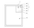
本実施形態では、通信用装置1は、一例として、図1に示すように、建物BDの窓ガラス10に設けられる。この場合、通信用装置1は、建物BDのすべての窓ガラス10に対して設けられてもよいが、図1に示すように、一部の窓ガラス10に対して設けられてよい。例えば、通信用装置1が設けられる窓ガラス10は、不感地内の窓ガラス10や不感地周辺の窓ガラス10であってよい。なお、窓ガラス10の地上からの高さは、電波の効率性の点で、1~14mが好ましく、2~10mが特に好ましい。 In this embodiment, as an example, the
図2は、ある一の窓ガラス10に設けられる通信用装置1を概略的に示す図であり、窓ガラス10の表面に対して垂直方向に視た平面図である。図3は、図2の矢印A1の方向に視た概略図である。 FIG. 2 is a diagram schematically showing the
図2には、窓ガラス10とともにサッシ(枠体)7が示される。窓ガラス10は、透明である。なお、本明細書において、「透明」とは、可視光の透過率が50%以上である状態であるが、好ましくは、可視光の透過率が60%以上であり、より好ましくは、可視光の透過率が70%以上である。窓ガラス10は、複層ガラスであってもよいし、層数は任意である。また、変形例では、窓ガラス10に代えて、樹脂(例えば、ポリエチレンテレフタレート(PET)、ポリエチレン)、ガラス樹脂複合体(例えば、繊維強化プラスチック)又はセラミックス等の素材により形成される透明な板材が利用されてもよい。 FIG. 2 shows the
窓ガラス10の厚さは、任意である。窓ガラス10を形成するガラス板としては、透明な無機ガラスを例示することができる。無機ガラスとしては、通常のソーダライムガラス、ホウ珪酸ガラス、無アルカリガラス又は石英ガラス等を例示することができる。成形法についても特に限定されないが、例えば、フロート法によって製造されたフロート板ガラスを例示することができる。また、着色成分を添加しない無色透明な材質を用いてもよく、あるいは、着色された着色透明な材質を用いてもよい。 The thickness of the
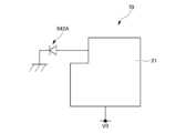
本実施形態では、一例として、通信用装置1は、図2に示すように、指向性制御アレイ20と、プリント基板30と、アンテナ部40と、処理装置50とを含む。 In this embodiment, as an example, the
指向性制御アレイ20は、反射型(リフレクトアレイ)である。指向性制御アレイ20は、窓ガラス10を誘電体の基材(可視光の透過率が50%以上である基材の一例)として形成される。指向性制御アレイ20は、窓ガラス10の全面に対して形成されてもよいし、図2に示すように、窓ガラス10の一部に対して形成されてもよい。ただし、指向性制御アレイ20は、好ましくは、図2に示すように、サッシ7に隣接する態様で形成される。この場合、サッシ7を利用して見栄えの良好な配線構造が容易に実現できる。指向性制御アレイ20の構造は後述する。なお、基材の可視光透過率は、透明性の点で、60%以上が好ましく、さらには70%以上が特に好ましい。 The
プリント基板30は、指向性制御アレイ20に関連する各種電子部品(処理装置50を含む)が実装される。プリント基板30は、指向性制御アレイ20と同様、窓ガラス10上に設けられる。ただし、変形例では、プリント基板30は、サッシ7内や他の箇所に配置されてもよい。 The printed
アンテナ部40は、図3に示すように、指向性制御アレイ20に向けて電波を放射する。アンテナ部40は、窓ガラス10上に設けられてもよいが、好ましくは、図3に示すように、サッシ7に設けられる。サッシ7に設けられる場合は、窓ガラス10に対するサッシ7の高さH1を利用して、窓ガラス10における比較的広い範囲(指向性制御アレイ20が形成される範囲)に電波を放射することが容易となる。なお、図3には、アンテナ部40からの電波の放射態様がハッチング領域S1で模式的に示される。 The
処理装置50は、プリント基板30上に実装される。なお、処理装置50の構成の一部は、プリント基板30とは別に実装されてもよい。処理装置50は、後述するが、指向性制御アレイ20で反射する電波の指向性を制御する。 The
なお、図2では、プリント基板30(及びそれに伴い処理装置50)は、窓ガラス10上に配置されるが、これに限られない。プリント基板30(及びそれに伴い処理装置50)の少なくとも一部(例えば直流電源生成部53)は、窓ガラス10に隣接する壁部や天井部、床部等のような他の箇所に配置されてもよい。この点、プリント基板30(及びそれに伴い処理装置50)の少なくとも一部(例えば直流電源生成部53)は、好ましくは、壁部内や、天井内、床下等のような、可視でないような箇所に配置され、この場合は、意匠性を高めることができる。また、同様の観点から、アンテナ部40は、窓ガラス10に隣接する壁部や天井部、床部等、あるいは、窓ガラス10に隣接しない壁部や天井部、床部等、のような他の箇所に配置されてもよい。 In addition, in FIG. 2, the printed circuit board 30 (and the
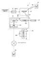
図4は、本実施形態の通信用装置1に関連する制御系と、通信用装置1を利用した通信形態を概略的に示す図である。図4には、2つのユーザ端末U1,U2が示される。以下では、区別のため、ユーザ端末U2を、「外部のユーザ端末U2」とも称する。図4では、外部のユーザ端末U2とユーザ端末U1とが通信している状況が示される。ユーザ端末U1は、例えば、建物BDの室内に存在するものとする(図5参照)。図4に関する説明において、特に言及しない限り、「受信」及び「送信」とは、ユーザ端末U1を基準とし、例えば「受信」は、ユーザ端末U1が外部のユーザ端末U2からデータ等を受信する際の「受信」を意味する。 FIG. 4 is a diagram schematically showing a control system related to the
図4に示すように、処理装置50は、マイクロコンピュータ51(以下、「MICOM51」と称する)(制御部の一例)と、通信回路部52と、直流電源生成部53(電源生成部の一例)とを含む。 As shown in FIG. 4, the
MICOM51は、指向性制御アレイ20の制御を行う。MICOM51には、外部入力として指向性指示(反射方向指示)が入力される。外部入力は、例えば建物BDを管理する管理コンピュータ(図示せず)やユーザ端末U1等から入力される。MICOM51は、指向性指示に基づいて、指向性制御アレイ20を制御する。この制御については図11等を参照して後述する。なお、MICOM51は、その他、通信回路部52等の制御も実行してもよい。MICOM51は、直流電源生成部53で生成された電源電圧V0に基づいて動作する。
通信回路部52は、通信インターフェース521と、ベースバンド回路部522と、RF回路部523とを含む。通信回路部52は、直流電源生成部53で生成された電源電圧V0に基づいて動作する。 The
通信回路部52は、通信インターフェース521を介して外部のネットワークNと接続し、ネットワークNを介して外部のユーザ端末U2と通信する。なお、通信回路部52で取り扱う通信は、音声通信やデータ通信など任意である。 The
なお、ネットワークNは、無線通信網や、インターネット、VPN(Virtual Private Network)、WAN(Wide Area Network)、有線ネットワーク、又はこれらの任意の組み合わせ等を含んでもよい。 Note that the network N may include a wireless communication network, the Internet, a VPN (Virtual Private Network), a WAN (Wide Area Network), a wired network, or any combination thereof.
外部のユーザ端末U2は、後述するユーザ端末U1とは異なる端末であり、ユーザ端末U1に対して例えば遠隔位置に位置する。従って、例えば外部のユーザ端末U2とユーザ端末U1とが通信している状況(図4に示す状況)では、外部のユーザ端末U2とユーザ端末U1の各ユーザは、異なるユーザであることが想定される。 The external user terminal U2 is a terminal different from the user terminal U1, which will be described later, and is located, for example, at a remote location with respect to the user terminal U1. Therefore, for example, in a situation where the external user terminal U2 and the user terminal U1 are communicating (the situation shown in FIG. 4), it is assumed that the users of the external user terminal U2 and the user terminal U1 are different users. be.
通信インターフェース521は、ネットワークNと接続するためのインターフェースである。 The
ベースバンド回路部522は、IPパケットとベースバンド信号とを相互に変換する処理を行う。 The
RF回路部523は、ベースバンド回路部522から受信したベースバンド信号に対して、D/A(Digital-to-Analog)変換、変調、周波数変換、及び電力増幅等を行うことでアンテナ部40から送信すべき無線信号(RF信号)を生成する。また、RF回路部523は、アンテナ部40により受信した無線信号に対して、周波数変換、A/D(Analog to Digital)変換、復調等を行うことでベースバンド信号を生成し、ベースバンド回路部522に与える。 The
外部のユーザ端末U2からデータ等の受信の際、ベースバンド回路部522は、通信インターフェース521を介して得た受信データに基づいて、当該受信データに応じたベースバンド信号を生成して、RF回路部523に与える。この場合、RF回路部523は、ベースバンド回路部522からのベースバンド信号に基づいて、当該ベースバンド信号に応じた無線信号を生成し、生成した無線信号に応じた送信電波をアンテナ部40を介して放射する(図4のR1参照)。 When receiving data or the like from the external user terminal U2, the
外部のユーザ端末U2へのデータ等の送信の際、RF回路部523は、アンテナ部40を介して受信した電波(ユーザ端末U1からの電波)に応じたベースバンド信号を生成してベースバンド回路部522に与える。ベースバンド回路部522は、RF回路部523を介して得たベースバンド信号に基づいて、外部のユーザ端末U2への送信データを生成し、生成した送信データを通信インターフェース521を介して外部のユーザ端末U2へ送信する。 When transmitting data or the like to the external user terminal U2, the
直流電源生成部53は、図4に示すように、外部電源である例えば交流電源600(建物BDに供給される交流電源)に電気的に接続され、交流電源600に基づいて直流の電源電圧V0を生成する。直流電源生成部53が生成する電源電圧V0は、MICOM51及び通信回路部52の動作だけでなく、指向性制御アレイ20の動作にも利用される。指向性制御アレイ20の動作について後に詳説する。 As shown in FIG. 4, the DC
図5は、通信用装置1の動作の説明図であり、通信用装置1が窓ガラス10に設けられる室内の状態を模式的に示す図である。図5には、通信用装置1の指向性制御アレイ20からユーザ端末U1に送信される電波(図4の矢印R2参照)の放射態様が、ハッチング領域S2で模式的に示される。 FIG. 5 is an explanatory diagram of the operation of the
受信の際は、指向性制御アレイ20は、アンテナ部40からの電波が入射されると(図3参照)、当該電波に基づいて、室内側に向かう反射波を出力する(図4の矢印R2、図5のS2参照)。例えば、アンテナ部40からは、上述のように、外部のユーザ端末U2からの受信データに係る電波が指向性制御アレイ20に向けて放射される。従って、この場合、室内のユーザ端末U1は、指向性制御アレイ20からの反射波を受信することで、外部のユーザ端末U2からの受信データを受信できる。 When receiving radio waves from the antenna unit 40 (see FIG. 3), the
また、送信の際は、指向性制御アレイ20は、ユーザ端末U1からの電波が入射されると(図4の矢印R2参照)、当該電波に基づいて、アンテナ部40に向かう反射波を出力する(図4の矢印R1参照)。例えば、ユーザ端末U1からは、上述のように、外部のユーザ端末U2への送信データに係る電波が放射され、指向性制御アレイ20に入射する。従って、この場合、アンテナ部40が指向性制御アレイ20からの反射波を受信することで、通信用装置1は、外部のユーザ端末U2へと送信データを(通信回路部52及びネットワークNを介して)送信できる。 Also, during transmission, when radio waves from the user terminal U1 are incident (see arrow R2 in FIG. 4), the
このような図4に示す通信形態によれば、ユーザ端末U1と外部のユーザ端末U2とは、通信用装置1を介して通信可能となる。具体的には、窓ガラス10を利用して形成される指向性制御アレイ20を利用して、室内のユーザ端末U1と、外部のユーザ端末U2との間で通信を成立させることができる。このようにして、通信用装置1は、基地局装置として機能でき、ユーザ端末U1が上述のような不感地に位置する場合でも、外部のユーザ端末U2との間で通信を成立させることができる。 According to the communication mode shown in FIG. 4, the user terminal U1 and the external user terminal U2 can communicate with each other via the
次に、図6以降を参照して、指向性制御アレイ20について更に説明する。 Next, the
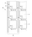
図6は、図2のQ1部の拡大図であり、指向性制御アレイ20の説明図である。図7は、図6のラインB-Bに沿った断面図である。なお、図6は、窓ガラス10の室内側から視た平面図であるものとする。また、図6では、図8Aを参照して後述する配線部90及びスイッチ回路94の図示は省略されている。 FIG. 6 is an enlarged view of the Q1 portion of FIG. 2 and is an explanatory view of the
図6に示すように、指向性制御アレイ20は、窓ガラス10上に形成される複数の導電体21を含む。複数の導電体21は、それぞれが後述の一の単位素子70を形成し、所定の2次元パターンで設けられる。所定の2次元パターンは、図6に示すような各種パラメータp1,p2,g1,g2等で決まる。なお、前出の図3(後出の図10A等も同様)では、指向性制御アレイ20を形成する薄い導電体21等は図示が省略されている。 As shown in FIG. 6,
パラメータp1は、導電体21間の縦方向のピッチであり、パラメータp2は、導電体21間の横方向のピッチであり、パラメータg1は、導電体21間の縦方向の離間距離であり、パラメータg2は、導電体21間の横方向の離間距離である。なお、パラメータp1とパラメータg1は、導電体21の縦方向の寸法が影響するパラメータであるが、導電体21の縦方向の寸法が新たなパラメータとして利用されてもよい。導電体21の横方向の寸法についても同様である。 The parameter p1 is the vertical pitch between the
各種パラメータp1,p2,g1,g2は、一定である必要はなく、後述のように、後述の複数の単位素子70への電圧印加パターンごとに所望の指向性が実現されるように適合される。なお、図6では、複数の導電体21は、平面視で矩形の形態であるが、矩形である必要はなく、また、複数の導電体21の形状も一定である必要はない。また、複数の導電体21の一部又は全部は、立体的な構成(すなわち窓ガラス10の表面に対して垂直方向に特徴的な形状)を有してもよい。 Various parameters p1, p2, g1, and g2 do not need to be constant, and are adapted so as to achieve desired directivity for each voltage application pattern to a plurality of
また、指向性制御アレイ20は、図7に示すように、窓ガラス10を挟んで複数の導電体21に対向するように、グランド用の導電体22が形成される。すなわち、窓ガラス10における室外側の表面には、複数の導電体21に対向する領域(すなわち指向性制御アレイ20の形成領域)に導電体22が形成される。ただし、変形例では、導電体22は省略されてもよい。なお、導電体22は、複数に分割されない形態であるが、導電体21と同様に分割されてもよい。 In the
ここで、本実施形態では、複数の導電体21及び導電体22は、好ましくは、透明である。これにより、窓ガラス10における複数の導電体21及び導電体22が設けられる領域(すなわち窓ガラス10における指向性制御アレイ20が設けられる領域)を透明とすることが可能となる。すなわち、複数の導電体21及び導電体22は、窓ガラス10の可視光の透過率を大きく低下させることなく、窓ガラス10上に設けることができる。このようにして、指向性制御アレイ20は、窓ガラス10の可視光の透過率を大きく低下させることなく、窓ガラス10を利用して成立することができる。 Here, in this embodiment, the plurality of
複数の導電体21及び導電体22としては、例えば酸化スズドープ酸化インジウム(ITO)、酸化スズなどの酸化物からなる導電体やLow-Eのような多層からなる導電体を使用できる。Low-Eとは、Low emissivityの略であり、導電性の透明酸化膜や、膜厚約10nmの銀膜を誘電体層で挟み、可視域で低反射率、赤外域で高反射率とした銀多層膜をコートしたものが知られている。複数の導電体21及び導電体22の厚さは、特に限定されるものではないが、一例として0.002mm~0.020mmである。なお、複数の導電体21及び導電体22の厚さが0.020mm以下であれば、エッチング等によるパターニングがしやすくなる。導電体21の導電性は、アレイとしての性能の点で、シート抵抗が、10Ω/sq以下であることが好ましく、1Ω/sq以下であることがより好ましく、0.1Ω/sq以下であることが最も好ましい。導電体22の導電性は、性能の点で、シート抵抗が、10Ω/sq以下であることが好ましく、1Ω/sq以下であることがより好ましく、0.1Ω/sq以下であることが最も好ましい。 As the plurality of
複数の導電体21は、それぞれ、メッシュ状に形成されてもよい。複数の導電体21のそれぞれをメッシュ状に形成することにより、複数の導電体21の透視性及び透光性(及びそれに伴い窓ガラス10における指向性制御アレイ20が設けられる領域での透視性及び透光性)を高めることができる。 Each of the plurality of
複数の導電体21のそれぞれがメッシュ状に形成される場合、メッシュの目は方形であってもよく、菱形であってもよい。メッシュの目を方形に形成する場合、メッシュの目は正方形であることが好ましい。メッシュの目が正方形であれば、意匠性が良い。また、自己組織化法によるランダム形状でもよい。ランダム形状にすることでモアレを防ぐことができる。メッシュの線幅は、5~30μmが好ましく、6~15μmがより好ましい。メッシュの線間隔は、50~500μmが好ましく、100~300μmがより好ましい。 When each of the plurality of
また、導電体22についても、複数の導電体21のそれぞれと同様に、メッシュ状に形成されてもよい。 Further, the
図8Aは、単位素子70と配線部90の一例を示す説明図である。図8Bは、単位素子70のスイッチ回路94の一例を示す説明図である。図8Aには、複数の単位素子70が示される。 FIG. 8A is an explanatory diagram showing an example of the
単位素子70は、メタサーフェスの単位素子として機能可能であり、複数の導電体21ごとに形成される。一の単位素子70は、一の導電体21と、当該一の導電体21に電気的に接続される一のスイッチ回路94とを含む。複数の単位素子70は、それぞれが1つずつ導電体21を含む形で、アレイ状に配列されることで指向性制御アレイ20を形成する。 The
単位素子70のスイッチ回路94は、任意の態様で実現されてよい。例えば図8Bに示す例では、スイッチ回路94は、ダイオード942と、容量性素子943とを含む。ダイオード942は、カソード側がグランドに電気的に接続され、アノード側が容量性素子943を介して導電体21に電気的に接続される。電源ライン92は、一端がダイオード942と容量性素子943の間に電気的に接続される。この場合、ダイオード942に電源電圧V0が印加されると、当該ダイオード942を含む単位素子70(導電体21及びスイッチ回路94)がメタサーフェスとして機能する。他方、ダイオード942に電圧が印加されない場合は、当該ダイオード942を含む単位素子70(導電体21及びスイッチ回路94)は、メタサーフェスとして機能しない。スイッチ回路94は、このような構成に限られず、例えばトランジスタのような半導体スイッチ素子や、MEMS(Micro Electro Mechanical Systems)スイッチ等を含んでもよい。また、トランジスタの場合、トランジスタは、薄膜デバイスとして導電体21と一体に形成されてもよい。 The
なお、以下では、ある一の単位素子70に電源電圧V0(又は直流電圧)が印加されるとは、当該一の単位素子70のダイオード942に電源電圧V0(又は直流電圧)が印加されることを意味する。 In the following description, applying the power supply voltage V0 (or the DC voltage) to a
配線部90は、直流電源生成部53により生成される電源電圧V0に電気的に接続される。配線部90は、複数の単位素子70のうちの、所定の単位素子70だけに直流電圧が印加できるように形成される。また、配線部90は、好ましくは、複数の単位素子70のうちの、直流電圧の印加される単位素子70のパターンが複数種類存在するように設定される(図9参照)。
具体的には、配線部90は、グランドライン91と、電源ライン92とを含む。電源ライン92及びグランドライン91は、対応するスイッチ回路94を介して、対応する単位素子70に接続される。グランドライン91は、グランドに電気的に接続され、電源ライン92は、電源電圧V0に電気的に接続される。この場合、ある単位素子70のスイッチ回路94に電源電圧V0を印加すると、当該単位素子70のスイッチ回路94のダイオード942に、電源電圧V0が印加されることになる。なお、グランドライン91は、ビア等により導電体22に電気的に接続されてもよいし、電源ライン92と同様の態様で窓ガラス10上に形成されてもよい。なお、窓ガラス10上にグランドライン91及び電源ライン92を形成する場合、電源ライン92とグランドライン91とが交差する領域では、絶縁膜等が設けられてよい。 Specifically, the
なお、電源ライン92は、複数の単位素子70のそれぞれに対して設けられてもよいが、複数の単位素子70のうちの、同時に電源電圧V0が印加される単位素子70(すなわち、ある一の電圧印加パターンのときに電源電圧V0を印加される単位素子70)は、共通の電源ライン92により電気的に接続されてもよい。 Note that the
配線部90の電源ライン92は、好ましくは、複数の導電体21と同様、透明である。この場合、電源ライン92は、窓ガラス10の可視光の透過率を大きく低下させることなく、窓ガラス10上に配置されることができる。すなわち、指向性制御アレイ20に係る配線部90は、窓ガラス10の可視光の透過率を大きく低下させることなく、窓ガラス10を利用して成立することができる。 The
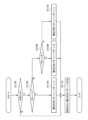
ここで、図9~図10Dを参照して、電圧印加パターンと指向性制御アレイ20で実現される指向性(反射角度)との関係について説明する。 Here, the relationship between the voltage application pattern and the directivity (reflection angle) realized by the
図9は、制御用のマップ情報の説明図であり、指示IDと電圧印加パターンとの関係の一例を示す図である。 FIG. 9 is an explanatory diagram of map information for control, and is a diagram showing an example of the relationship between an instruction ID and a voltage application pattern.
図9では、指示IDは、指向性指示に含まれる情報であり、電圧印加パターンは、複数の単位素子70のうちの、直流電圧の印加される単位素子70のパターンを示す。電圧印加パターンは、指示IDに対応付けられる態様で、指示IDごとに用意される。図9では、指示ID“0001”には、電圧印加パターン“パターンA”が対応付けられ、指示ID“0002”には、電圧印加パターン“パターンB”が対応付けられ、といった具合である。なお、電圧印加パターンの数は、指向性制御アレイ20により実現される指向性の種類の数に対応し、好ましくは、多様な指向性が実現可能なように、2つ以上であってよい。 In FIG. 9 , the instruction ID is information included in the directivity instruction, and the voltage application pattern indicates the pattern of the
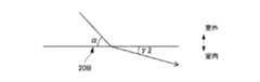
図10A及び図10Bは、電圧印加パターンの相違によって実現される指向性制御アレイ20の反射角度の相違(変化)を示す図であり、図10C及び図10Dは、電圧印加パターンの説明図である。図10A及び図10Bは、窓ガラス10の断面視で、指向性制御アレイ20における反射角度を説明する図である。図10C及び図10Dには、図8A及び図8Bで示した単位素子70のそれぞれが、1つの矩形単位で非常に模式的に示されている。なお、図10C及び図10Dでは、説明の便宜上、複数の単位素子70は、同じ大きさかつ同じ形状で、同じ間隔で配置されているが、上述のように、複数の導電体21は、多様に設定されるパラメータに基づいて構成される。 10A and 10B are diagrams showing differences (changes) in reflection angles of the
図10C及び図10Dでは、複数の単位素子70のうちの、直流電圧の印加される単位素子70がハッチングで示される。 In FIGS. 10C and 10D, among the plurality of
ここでは、説明の便宜上、図10Cは、電圧印加パターン“パターンA”に対応し、図10Aは、電圧印加パターン“パターンA”のときの反射角度を表す。また、図10Dは、電圧印加パターン“パターンB”に対応し、図10Bは、電圧印加パターン“パターンB”のときの反射角度を表す。なお、この場合、“パターンA”に対しては、複数の単位素子70のうちの、図10Cでハッチングされている単位素子70が、直流電圧の印加対象の単位素子70として対応付けられる。同様に、“パターンB”に対しては、複数の単位素子70のうちの、図10Dでハッチングされている単位素子70が、直流電圧の印加対象の単位素子70として対応付けられる。 Here, for convenience of explanation, FIG. 10C corresponds to the voltage application pattern “Pattern A”, and FIG. 10A shows the reflection angle at the time of the voltage application pattern “Pattern A”. Also, FIG. 10D corresponds to the voltage application pattern "Pattern B", and FIG. 10B shows the reflection angle for the voltage application pattern "Pattern B". In this case, the
図10A~図10Dの場合、電圧印加パターン“パターンA”であるとき、指向性制御アレイ20に対して入射角度(90-α)で入射した電波は、図10Aに示すように、指向性制御アレイ20から反射角度(90-β1)で出力される。また、電圧印加パターン“パターンB”であるとき、指向性制御アレイ20に対して入射角度(90-α)で入射した電波は、図10Bに示すように、指向性制御アレイ20から反射角度(90-β2)で出力される。このとき、β1≠β2である。 In the case of FIGS. 10A to 10D, when the voltage application pattern is “Pattern A”, radio waves incident on the
このように、指向性制御アレイ20では、電圧印加パターンを変化させることで、反射角度を変化させることができる。そして、反射角度は、直流電圧が印加される各単位素子70に係る導電体21の位相差を調整することで、自由に設計できる。例えば、電圧印加パターン“パターンA”に関しては、電圧印加パターン“パターンA”のときに直流電圧が印加される各単位素子70(図10Cでハッチングされている各単位素子70)に係る導電体21の位相差を調整することで、反射角度(90-β1)を所望の値に調整できる。ここで、各単位素子70に係る導電体21の位相差は、図6を参照して上述した導電体21に係る各種パラメータp1,p2,g1,g2等を調整することで、調整できる。このようにして、この種の指向性制御アレイ20では、メタマテリアルないしメタサーフェスの性質を利用して、各種パラメータp1,p2,g1,g2等を調整することで、反射角度を調整することができる。 In this manner, the
なお、同じ入射角度(90-α)であるときに電圧印加パターンに応じて反射角度が変化するということは、指向性制御アレイ20から出力される電波の指向性が、電圧印加パターンに応じて変化することを意味する。従って、この種の指向性制御アレイ20では、各種パラメータp1,p2,g1,g2等を調整することで、電圧印加パターンごとの指向性を調整することができる。そして、電圧印加パターンを変化させることで、動的に指向性を変化させることができる。 The fact that the angle of reflection changes according to the voltage application pattern when the incident angle (90-α) is the same means that the directivity of the radio wave output from the
次に、図11を参照して、本実施形態の通信用装置1の動作例(指向性制御アレイ20の制御例)について説明する。 Next, with reference to FIG. 11, an operation example (control example of the directivity control array 20) of the
図11は、MICOM51により実行される指向性制御処理の一例を示すフローチャートである。ここでは、一例として、電圧印加パターンが“パターンA”~“パターンC”の3種類だけ用意されているものとする。 FIG. 11 is a flow chart showing an example of directivity control processing executed by the
ステップS1100では、MICOM51は、外部入力(指向性指示)が受信されたか否かを判定する。外部入力は、任意の外部装置からの入力であってよく、例えばユーザ端末U1からの入力であってもよい。判定結果が“YES”の場合、ステップS1102に進み、それ以外の場合は、ステップS1112に進む。 In step S1100, the
ステップS1102では、MICOM51は、指向性指示に含まれる指示IDが“0001”(図9参照)であるか否かを判定する。すなわち、MICOM51は、“パターンA”が指示されているか否かを判定する。判定結果が“YES”の場合、ステップS1104に進み、それ以外の場合は、ステップS1106に進む。 In step S1102, the
ステップS1104では、MICOM51は、電圧印加パターンを“パターンA”に設定する。なお、電圧印加パターンの初期値(デフォルト値)は、例えば“パターンA”であってよい。 In step S1104, the
ステップS1106では、MICOM51は、指向性指示に含まれる指示IDが“0002”(図9参照)であるか否かを判定する。すなわち、MICOM51は、“パターンB”が指示されているか否かを判定する。判定結果が“YES”の場合、ステップS1108に進み、それ以外の場合(すなわち“パターンC”が指示されている場合)は、ステップS1110に進む。 In step S1106, the
ステップS1108では、MICOM51は、電圧印加パターンを“パターンB”に設定する。 In step S1108, the
ステップS1110では、MICOM51は、電圧印加パターンを“パターンC”に設定する。 In step S1110, the
ステップS1112では、MICOM51は、現在の設定された電圧印加パターンに基づいて、複数の単位素子70に印加する直流電圧を制御する。例えば、現在の設定された電圧印加パターンが“パターンA”である場合、MICOM51は、複数の単位素子70のうちの、“パターンA”に対応付けられる単位素子70に対して、直流電圧を印加する。 In step S1112, the
このようにして、図11に示す処理によれば、外部入力(指向性指示)に応じて、電圧印加パターン及びそれに伴い指向性制御アレイ20の指向性を変化させることができる。従って、例えば、室内でのユーザ端末U1の位置に応じた外部入力(指向性指示)を入力することで、室内でのユーザ端末U1の位置に応じた指向性を有するように指向性制御アレイ20の指向性を調整できる。 In this manner, according to the processing shown in FIG. 11, the voltage application pattern and the directivity of the
なお、上述した実施形態では、外部のユーザ端末U2が、ユーザ端末U1と通信する相手側として例示されているが、通信用装置1を利用してユーザ端末U1と通信可能な対象は、任意である。例えば、通信用装置1を利用してユーザ端末U1は、各種のサーバと通信することも可能である。なお、外部のユーザ端末U2(ユーザ端末U1についても同様)は、任意であり、スマートフォン、タブレット、PC(パーソナルコンピュータ)、ゲーム機、ウエアラブルデバイス等のような、通信機能を持つ任意の端末であってよい。 In the above-described embodiment, the external user terminal U2 is exemplified as the other party to communicate with the user terminal U1. be. For example, using the
以上説明した本実施形態によれば、とりわけ、以下のような優れた効果が奏される。 According to the present embodiment described above, the following excellent effects are exhibited.
本実施形態によれば、上述したように、窓ガラス10を利用して指向性制御アレイ20を形成できるので、建物BD等にすでにある窓ガラスを利用でき、窓ガラス10以外の誘電体の基材を、新たに用意する必要性を無くすことができる。ただし、変形例では、室内等に配置される間仕切り板や壁体の一部を基材として指向性制御アレイ20を形成してもよい。 According to this embodiment, as described above, since the
ところで、窓ガラス10のような、透明な基材を利用して指向性制御アレイ20を形成する場合、窓ガラス10の本来の機能を可能な限り損なわないように指向性制御アレイ20を形成することが有用である。例えば、指向性制御アレイ20を形成する導電体21等が非透明である場合、窓ガラス10の本来の機能を比較的大きく損なうおそれがある。 By the way, when the
この点、本実施形態によれば、上述したように、透明な導電体21及び22が形成されるので、窓ガラス10の可視光の透過率を大きく低下させることなく、窓ガラス10に導電体21及び22を形成できる。また、配線部90の電源ライン92が透明である場合は、窓ガラス10の可視光の透過率を大きく低下させることなく、窓ガラス10に配線部90を形成できる。これにより、窓ガラス10の本来の機能を損なうことなく、窓ガラス10を利用して指向性制御アレイ20を形成できる。 In this respect, according to the present embodiment, as described above, the
また、本実施形態においては、処理装置50の一部又は全部を、壁部内等の、可視でない箇所に配置する場合には、指向性制御アレイ20を制御するための構成に起因した見栄えの悪化を防止できる。例えば、直流電源生成部53を窓ガラス10の外側(例えばサッシ7内)に配置し、指向性制御アレイ20を形成する複数の単位素子70への直流電圧の印加のための配線部90と、直流電源生成部53との間の配線等を、サッシ7を利用して配索することで、見栄えを良好に保ちつつ、窓ガラス10を利用して指向性制御アレイ20を形成できる。 In addition, in this embodiment, if a part or all of the
また、本実施形態によれば、上述したように、不感地に存在するユーザ端末U1が外部のユーザ端末U2と通信可能となるので、不感地の問題を低減できる。周波数が高くなるほど不感地が多くなるので、特に、将来の高速・広帯域通信システムの実現に向けて周波数が高くなると、不感地の問題が顕著となり得る。この点、本実施形態によれば、窓ガラス10のような既存の物体を利用して、不感地での良好な通信環境を確保できる。 Further, according to this embodiment, as described above, the user terminal U1 existing in the dead area can communicate with the external user terminal U2, so that the problem of the dead area can be reduced. Since the higher the frequency, the more the dead area, the problem of the dead area can become significant especially when the frequency is increased toward the realization of future high-speed and wideband communication systems. In this respect, according to the present embodiment, an existing object such as the
なお、本実施形態では、指向性制御アレイ20は、室内側のアンテナ部40から入射される電波に基づいて、室内側に電波を出力するように構成されているが、これに限られない。例えば、アンテナ部40を室外側に配置し(配置に関して図13のアンテナ部40B参照)、指向性制御アレイ20Bは、室外側のアンテナ部40から入射される電波に基づいて、室外側に電波を出力するように構成されてもよい。かかる構成は、ユーザ端末U1が、建物BDの室内ではなく、建物BDの外部、例えば建物BDの前を通る道路(特に不感地内の道路)上に存在する場合等に好適となる。すなわち、通信用装置1は、建物BDの外部の不感地に対しても機能するように構成することもできる。 In this embodiment, the
ところで、指向性制御アレイ20を設けずに、アンテナ部40から直接的に室内側に電波を放射する構成(すなわちアンテナ部40から室内に電波を放射する構成)では、電波法等の関係もあり、室内の広範囲をカバーする態様で電波を放射することが難しい。また、かかる構成では、室内の広範囲をカバーしようとすると、壁などから反射することにより(遅れて入射する電波のためS/N比が劣化して)干渉問題なども発生する。 By the way, in a configuration in which radio waves are directly radiated indoors from the
この点、本実施形態によれば、指向性制御アレイ20を用いるので、アンテナ部40から直接的に室内側に電波を放射する構成で生じる上述の不都合を低減できる。また、例えばユーザ端末U1の位置に応じて指向性制御アレイ20の指向性を動的に制御することも可能となり、この場合、ビームフォーミングと同様の効果を実現することも可能である。 In this respect, according to the present embodiment, since the
[実施形態2]
次に、実施形態2について説明する。本実施形態に関しては、上述した実施形態1と同様であってよい構成要素については、同一の参照符号を付して説明を省略する場合がある。[Embodiment 2]
Next,
図12は、本実施形態の通信用装置1Aに関連する制御系と、通信用装置1Aを利用した通信形態を概略的に示す図である。 FIG. 12 is a diagram schematically showing a control system related to the
実施形態2による通信用装置1Aは、上述した実施形態1による通信用装置1に対して、アンテナ部40を備えず、指向性制御アレイ20が指向性制御アレイ20Aで置換され、かつ、処理装置50が処理装置50Aで置換された点が異なる。 The
処理装置50Aは、上述した実施形態1による処理装置50に対して、通信回路部52が省略される点が異なる。 The
指向性制御アレイ20Aは、反射型(リフレクトアレイ)である。指向性制御アレイ20Aは、上述した実施形態1による指向性制御アレイ20に対して、構成や配置は同じであり、機能だけが異なる。具体的には、上述した実施形態1による指向性制御アレイ20は、アンテナ部40とユーザ端末U1との間での電波の送受に介在するのに対して、指向性制御アレイ20Aは、基地局BSとユーザ端末U1との間での電波の送受に介在する。すなわち、指向性制御アレイ20Aは、基地局BSとユーザ端末U1との間の中継器として機能する。 The
ただし、本実施形態においては、指向性制御アレイ20Aは、窓ガラス10の室外側に単位素子70が配置されるように、上述した実施形態1による指向性制御アレイ20に対して、導電体21及び導電体22に関する室内外の配置が逆であってもよい。 However, in this embodiment, the
実施形態2による通信用装置1Aは、ユーザ端末U1が、建物BDの室内ではなく、建物BDの外部、例えば建物BDの前を通る道路(特に不感地内の道路)上に存在する場合等に好適である。 The
受信の際は、指向性制御アレイ20Aは、基地局BSからの電波が入射されると、当該電波に基づいて、反射波を出力する。例えば、基地局BSからは、外部のユーザ端末U2からの受信データに係る電波が放射される。従って、この場合、ユーザ端末U1は、指向性制御アレイ20Aからの反射波を受信することで、外部のユーザ端末U2からの受信データを受信できる。 During reception, when radio waves from the base station BS are incident on the
また、送信の際は、指向性制御アレイ20Aは、ユーザ端末U1からの電波が入射されると、当該電波に基づいて、基地局BSに向かう反射波を出力する。例えば、ユーザ端末U1からは、上述のように、外部のユーザ端末U2への送信データに係る電波が放射され、指向性制御アレイ20Aに入射する。従って、この場合、基地局BSは、指向性制御アレイ20Aからの反射波を受信することで、外部のユーザ端末U2へと送信データを送信できる。 Also, during transmission, when radio waves from the user terminal U1 are incident on the
このようにして、本実施形態においても、ユーザ端末U1は、指向性制御アレイ20A及び基地局BSを介して、外部のユーザ端末U2と通信することが可能である。具体的には、窓ガラス10を利用して形成される指向性制御アレイ20Aを利用して、ユーザ端末U1(本実施形態の場合、建物BDの外部に位置するユーザ端末U1)と、外部のユーザ端末U2との間で通信を成立させることができる。このようにして、通信用装置1は、基地局装置として機能でき、ユーザ端末U1が上述のような不感地に位置する場合でも、外部のユーザ端末U2との間で通信を成立させることができる。 Thus, also in this embodiment, the user terminal U1 can communicate with the external user terminal U2 via the
[実施形態3]
次に、実施形態3について説明する。本実施形態に関しては、上述した実施形態1と同様であってよい構成要素については、同一の参照符号を付して説明を省略する場合がある。[Embodiment 3]
Next,
図13は、本実施形態の通信用装置1Bの説明図であり、本実施形態の場合の図2の矢印A1の方向に視た概略図に対応する。 FIG. 13 is an explanatory diagram of the
実施形態3による通信用装置1Bは、上述した実施形態1による通信用装置1に対して、指向性制御アレイ20が指向性制御アレイ20Bで置換され、かつ、アンテナ部40がアンテナ部40Bで置換された点が異なる。 In the
指向性制御アレイ20Bは、上述した実施形態1による指向性制御アレイ20に対して、反射型ではなく、透過型である点が異なる。すなわち、指向性制御アレイ20Bは、室外側から入射した電波に基づいて、室内側に電波を放射するように構成される。透過型の構成は、反射型と同様、メタマテリアルないしメタサーフェスの性質を利用して、複数の導電体21に係る各種パラメータp1,p2,g1,g2等を調整することで構成できる。すなわち、各種パラメータp1,p2,g1,g2等を調整することで、複数の単位素子70からなるアレイ(裏側に導電体22が形成されるアレイ)を、反射型にしたり透過型にしたり自由に設計できる。 The
アンテナ部40Bは、上述した実施形態1によるアンテナ部40に対して、室外側から指向性制御アレイ20Bに電波を入射させるように配置される点が異なる。アンテナ部40Bは、例えば図13に示すように、サッシ7の室外側に設けられてもよい。この場合、指向性制御アレイ20Bは、室外側から窓ガラス10を透過して入射する電波に基づいて、室内側に電波を放射することになる。 The
図14A及び図14Bは、窓ガラス10の断面視で、指向性制御アレイ20Bにおける屈折角度を説明する図である。 14A and 14B are cross-sectional views of the
指向性制御アレイ20Bは、図14A及び図14Bに概念的に示すように、室外側から入射する電波の入射角度(90-α)が同じである場合でも、電圧印加パターンの相違に応じて、屈折角度が異なるように構成される。 As conceptually shown in FIGS. 14A and 14B, the
具体的には、図14Aは、電圧印加パターン“パターンA”のときの屈折角度を表し、図14Bは、電圧印加パターン“パターンB”のときの屈折角度を表すものとする。この場合、電圧印加パターン“パターンA”であるとき、指向性制御アレイ20Bに対して入射角度(90-α)で入射した電波は、図14Aに示すように、指向性制御アレイ20Bから屈折角度(90-γ1)で出力される。また、電圧印加パターン“パターンB”であるとき、指向性制御アレイ20Bに対して入射角度(90-α)で入射した電波は、図14Bに示すように、指向性制御アレイ20Bから屈折角度(90-γ2)で出力される。このとき、γ1≠γ2である。 Specifically, FIG. 14A represents the refraction angle for the voltage application pattern “pattern A”, and FIG. 14B represents the refraction angle for the voltage application pattern “pattern B”. In this case, when the voltage application pattern is “Pattern A”, the radio waves incident on the
このように、指向性制御アレイ20Bでは、電圧印加パターンを変化させることで、屈折角度を変化させることができる。そして、屈折角度は、直流電圧が印加される各単位素子70に係る導電体21の位相差を調整することで、自由に設計できる。例えば、電圧印加パターン“パターンA”に関しては、電圧印加パターン“パターンA”のときに直流電圧が印加される各単位素子70(図10Cでハッチングされている各単位素子70)に係る導電体21の位相差を調整することで、屈折角度(90-γ1)を所望の値に調整できる。このようにして、この種の指向性制御アレイ20Bでは、メタマテリアルないしメタサーフェスの性質を利用して、各種パラメータp1,p2,g1,g2等を調整することで、屈折角度を調整することができる。 Thus, in the
なお、反射の場合と同様に、同じ入射角度(90-α)であるときに電圧印加パターンに応じて屈折角度が変化するということは、指向性制御アレイ20Bから出力される電波の指向性が、電圧印加パターンに応じて変化することを意味する。従って、この種の指向性制御アレイ20Bでは、複数の導電体21に係る各種パラメータp1,p2,g1,g2等を調整することで、電圧印加パターンごとの指向性を調整することができる。そして、電圧印加パターンを変化させることで、動的に指向性を変化させることができる。 As in the case of reflection, the fact that the refraction angle changes according to the voltage application pattern when the incident angle (90-α) is the same means that the directivity of the radio wave output from the
本実施形態によれば、上述のように、窓ガラス10を基材として利用して上述した透過型の指向性制御アレイ20Bを形成できるので、上述した実施形態1と同様の効果が奏される。 According to the present embodiment, as described above, the above-described transmission-type
また、本実施形態による透過型の指向性制御アレイ20Bは、上述した実施形態2の指向性制御アレイ20Aに代えて利用されてもよい。この場合、上述した実施形態2は、上述した実施形態1と同様、ユーザ端末U1が室内に存在する場合に好適となる。 Also, the transmissive
次に、図16以降を参照して、本願発明者が実施したシミュレーション結果について説明する。ここでは、上述した実施形態1による指向性制御アレイ20に関するシミュレーション結果について説明するが、他の実施形態に関しても実質的に同様である。 Next, with reference to FIG. 16 and subsequent figures, the results of the simulation performed by the inventors of the present application will be described. Here, the simulation results for the
図16及び図17は、本シミュレーションで用いたモデルの説明図であり、一の単位素子70に関連したモデルを示す。本シミュレーションは、図示しないが、単位素子70は8×8のアレイで配置されたモデルを用いた。また、本シミュレーションでは、8×8のアレイに入射させる電波の周波数(動作周波数)は28GHzとし、偏波方向はエレベーション方向で計算した。同アレイにおいて、アジマス方向のピッチ(図6のパラメータp2参照)は、0.5λとし、エレベーション方向のピッチ(図6のパラメータp1参照)は、0.5λとした。なお、窓ガラス10に対応する基材の厚みは一定であるが、今回設計した例では厚みが大きいほど以下で説明する効果が得られる電波の周波数帯(帯域幅)を広げることができる。 16 and 17 are explanatory diagrams of the model used in this simulation, showing a model related to one
なお、本シミュレーションでは、図16及び図17に示すように、単位素子70の導電体21は、PINダイオード942Aを介して接地されるモデルとしている。なお、かかる構成は、導電体21をスルーホール(ビア)6600を介して導電体22(図7参照)に電気的に接続することで実現できる。 In this simulation, as shown in FIGS. 16 and 17, the
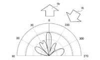
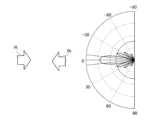
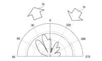
図18A~図18Dは、図18Eに示す電圧印加パターンを適用した場合のシミュレーション結果を示す図である。図18Aは、アジマス方向のRCS(Radar Cross Section)の特性(単位dB m2、以下同じ)を反射側の角度範囲で示し、図18Bは、エレベーション方向のRCSの特性を反射側の角度範囲で示す。ここでは、図18Aにて模式的に示すように、8×8の単位素子70のアレイには、アジマス方向の基準方向(0度の方向)に対して-30度をなす方向(330度)から電波を入射させた(図18C参照)。また、エレベーション方向では、基準方向(0度の方向)から電波を入射させた。図18A及び図18B(後出の同様の、図19A、図19B等も同様)では、電波の入射波は、矢印Riで模式的に示され、反射波は、矢印Rrで模式的に示される。なお、図18C(図18Dも同様)では、通信用装置1に対する電波の入射方向(図18Dでは、反射方向)が同様の矢印Ri、Rrで模式的に示される。なお、この場合、通信用装置1は、8×8の単位素子70のアレイを含む装置全体を表す。なお、これらは、後出の同様の図(図19C、図19D等)も同様である。18A to 18D are diagrams showing simulation results when the voltage application pattern shown in FIG. 18E is applied. FIG. 18A shows the characteristics of RCS (Radar Cross Section) in the azimuth direction (unit: dBm2 , hereinafter the same) in the angle range on the reflection side, and FIG. 18B shows the characteristics of the RCS in the elevation direction in the angle range on the reflection side. indicated by . Here, as schematically shown in FIG. 18A, the array of 8×8
なお、図18Eは、横方向をアジマス方向に対応させ、縦方向をエレベーション方向に対応させたときの、8×8の単位素子70のアレイにおける各単位素子70への電圧印加状態を示す。電圧印加状態は、“ON”と“OFF”の2種類であり、“ON”は、直流電圧が印加された状態を表し、“OFF”は、直流電圧が印加されていない状態を表す。“ON”状態の単位素子における反射位相と“OFF”状態の単位素子における反射位相は、およそ180°ずれるように設計している。例えば、図18Eの例では、アジマス方向で左から1列目と2列目と5列目と6列目はすべての単位素子70が“OFF”であり、残りのすべての単位素子70は“ON”である。なお、このような表記の意味は、後出の図19E及び図20Eについても同様である。 FIG. 18E shows the state of voltage application to each
図18Eに示す電圧印加パターンを適用した場合、図18A~図18Dに示すように、アジマス方向では、基準方向(0度の方向)に対して-30度をなす方向から電波を入射させると、アジマス方向の基準方向(0度の方向)への反射波が強くなる特性を示すシミュレーション結果が得られた。なお、単純な金属板に対して、アジマス方向で基準方向(0度の方向)に対して-30度をなす方向(330度)から電波を入射させると、基準方向(0度の方向)に対して30度をなす方向(30度)への反射が強くなる特性(図示せず)が得られる。このことから、上述した実施形態1による指向性制御アレイ20によれば、単純な金属板では得られない反射特性を実現できることがわかる。 In the case where the voltage application pattern shown in FIG. 18E is applied, as shown in FIGS. A simulation result was obtained showing the characteristic that the reflected wave in the reference direction (direction of 0 degrees) in the azimuth direction becomes stronger. In addition, when a radio wave is incident on a simple metal plate from a direction (330 degrees) forming -30 degrees with respect to the reference direction (direction of 0 degrees) in the azimuth direction, On the other hand, a characteristic (not shown) is obtained in which the reflection in the direction forming 30 degrees (30 degrees) is strong. From this, it can be seen that the
図19A~図19Dは、図19Eに示す電圧印加パターンを適用した場合のシミュレーション結果を示す図である。図19Aは、アジマス方向のRCSの特性を反射側の角度範囲で示し、図19Bは、エレベーション方向のRCSの特性を反射側の角度範囲で示す。ここでは、図19Aにて模式的に示すように、8×8の単位素子70のアレイには、図18A~図18Eに係るシミュレーションの場合と同様に、アジマス方向の基準方向(0度の方向)に対して-30度をなす方向(330度)から電波を入射させた(図19C参照)。また、エレベーション方向では、基準方向(0度の方向)から電波を入射させた。なお、図19C(図19Dも同様)では、8×8の単位素子70のアレイを含む通信用装置1に対する電波の入射方向(図19Dでは、反射方向)が模式的に示される。 19A to 19D are diagrams showing simulation results when the voltage application pattern shown in FIG. 19E is applied. FIG. 19A shows the RCS characteristics in the azimuth direction in the angle range on the reflection side, and FIG. 19B shows the RCS characteristics in the elevation direction in the angle range on the reflection side. Here, as schematically shown in FIG. 19A, the array of 8×8
図19Eに示す電圧印加パターンを適用した場合、図19A~図19Dに示すように、アジマス方向では、基準方向(0度の方向)に対して-30度をなす方向から電波を入射させると、アジマス方向の基準方向に対して20度をなす方向(20度の方向)への反射が強くなる特性を示すシミュレーション結果が得られた。このことから、上述した実施形態1による指向性制御アレイ20によれば、単純な金属板では得られない反射特性を実現できることがわかる。 When the voltage application pattern shown in FIG. 19E is applied, as shown in FIGS. 19A to 19D, in the azimuth direction, if radio waves are incident from a direction forming −30 degrees with respect to the reference direction (direction of 0 degrees), A simulation result was obtained showing a characteristic that the reflection in the direction forming 20 degrees with respect to the reference direction of the azimuth direction (the direction of 20 degrees) becomes stronger. From this, it can be seen that the
また、図19A~図19Eに係るシミュレーションは、図18A~図18Eに係るシミュレーションに対して、図18E及び図19Eを対比してわかるように、電圧印加パターンが異なる。そして、他の条件は同じである。従って、電圧印加パターンを変化させることで、反射角(反射方向)を変化させることができることがわかる。 Also, the simulations shown in FIGS. 19A to 19E differ from the simulations shown in FIGS. 18A to 18E in the voltage application pattern, as can be seen by comparing FIGS. 18E and 19E. And other conditions are the same. Therefore, it can be seen that the reflection angle (reflection direction) can be changed by changing the voltage application pattern.
図20A~図20Dは、図20Eに示す電圧印加パターンを適用した場合のシミュレーション結果を示す図である。図20Aは、アジマス方向のRCSの特性を反射側の角度範囲で示し、図20Bは、エレベーション方向のRCSの特性を反射側の角度範囲で示す。ここでは、図20Aにて模式的に示すように、8×8の単位素子70のアレイには、図18A~図18Eに係るシミュレーションの場合と同様に、アジマス方向の基準方向(0度の方向)に対して-30度をなす方向(330度)から電波を入射させた(図20C参照)。また、エレベーション方向では、基準方向(0度の方向)から電波を入射させた。なお、図20C(図20Dも同様)では、8×8の単位素子70のアレイを含む通信用装置1に対する電波の入射方向(図20Dでは、反射方向)が模式的に示される。 20A to 20D are diagrams showing simulation results when the voltage application pattern shown in FIG. 20E is applied. FIG. 20A shows the RCS characteristics in the azimuth direction in the angle range on the reflection side, and FIG. 20B shows the RCS characteristics in the elevation direction in the angle range on the reflection side. Here, as schematically shown in FIG. 20A, in the array of 8×8
図20Eに示す電圧印加パターンを適用した場合、図20A~図20Dに示すように、アジマス方向では、基準方向(0度の方向)に対して-30度をなす方向から電波を入射させると、アジマス方向で比較的広い角度範囲わたり反射が均一化される特性を示すシミュレーション結果が得られた。このことから、上述した実施形態1による指向性制御アレイ20によれば、単純な金属板では得られない反射特性を実現できることがわかる。 When the voltage application pattern shown in FIG. 20E is applied, as shown in FIGS. 20A to 20D, in the azimuth direction, if radio waves are incident from a direction forming −30 degrees with respect to the reference direction (direction of 0 degrees), Simulation results have been obtained that show the uniformity of the reflection over a relatively wide range of angles in the azimuth direction. From this, it can be seen that the
また、図20A~図20Eに係るシミュレーションは、図18A~図18Eに係るシミュレーションや図19A~図19Eに係るシミュレーションに対して、図18E、図19E、及び図20Eを対比してわかるように、電圧印加パターンが異なる。そして、他の条件は同じである。従って、電圧印加パターンを変化させることで、反射角(反射方向)を変化させるのみならず、指向性(及びそれに伴いカバレッジ)を変化させることができることがわかる。すなわち、図20Eに示す電圧印加パターンを適用した場合、図18Eや図19Eに示す電圧印加パターンを適用した場合に比べて、カバレッジを拡張できる。 Also, the simulations shown in FIGS. 20A to 20E are compared with the simulations shown in FIGS. 18A to 18E and the simulations shown in FIGS. 19A to 19E, as can be seen by comparing FIGS. The voltage application pattern is different. And other conditions are the same. Therefore, by changing the voltage application pattern, it is possible to change not only the reflection angle (reflection direction) but also the directivity (and thus the coverage). That is, when the voltage application pattern shown in FIG. 20E is applied, coverage can be expanded compared to the case where the voltage application patterns shown in FIGS. 18E and 19E are applied.
このような、カバレッジを拡張できる電圧印加パターンは、比較的高い周波数を扱う通信に好適である。これは、周波数が高くなるにつれて、反射や回折による伝搬損失が大きくなり、このような不感地が発生しやすくなるためである。例えば、図21に示すように、障害物2100により不感地が生じやすい環境下では、窓ガラス10への電波の伝播経路が制限されているものの、窓ガラス10には、障害物2100の間を通って電波が入射する(図21の矢印Ri参照)。このような環境下では、カバレッジを拡張できる電圧印加パターンを適用すると、図21に反射波を波面Rrで模式的に示すように、通信用装置1から不感地に向けて等方的に反射波を形成できる。これにより、障害物2100に起因して生じうる不感地を効果的に低減できる。 Such a voltage application pattern that can extend coverage is suitable for communications that handle relatively high frequencies. This is because the higher the frequency, the greater the propagation loss due to reflection and diffraction, and the more likely this type of dead area will occur. For example, as shown in FIG. 21 , in an environment where an
以上、各実施形態について詳述したが、特定の実施形態に限定されるものではなく、特許請求の範囲に記載された範囲内において、種々の変形及び変更が可能である。また、前述した実施形態の構成要素を全部又は複数を組み合わせることも可能である。 Although each embodiment has been described in detail above, it is not limited to a specific embodiment, and various modifications and changes are possible within the scope described in the claims. It is also possible to combine all or more of the constituent elements of the above-described embodiments.
例えば、上述した各実施形態では、指向性制御アレイ20、20A、及び20Bは、窓ガラス10を基材として形成されているが、これに限られない。例えば、指向性制御アレイ20、20A、及び20Bは、ガラスや樹脂等の透明な板材を基材として形成され、任意の場所に配置されてもよい。例えば、図15に模式的に示すように、基材10Aを利用して指向性制御アレイ20を形成し、当該基材10Aが、部屋の壁150に取付けられてもよい。この場合も、当該部屋が不感地である場合でも、室内のユーザ端末U1は、外部のユーザ端末U2との間で同様に通信を行うことができる。なお、図15に示す例では、壁150に取付けられているが、ディスプレイのような他の表面に取り付けられてもよいし、自動車や航空機、鉄道、船舶等のような移動体に取り付けられてもよい。 For example, in each of the embodiments described above, the
また、指向性制御アレイ20、20A、及び20Bは、透明なフィルムを基材として形成されてもよい。この場合、透明なフィルムは、フレキシブルなフィルム状の誘電体シート(例えばフッ素系樹脂のシート)であってもよい。例えば透明なフィルムは、フッ素系の低損失の接着層を含み、当該接着層を利用して窓ガラス10に接着されてよいし、他の箇所に貼り付けられてもよい。 Also, the
また、上述した実施形態では、指向性指示は、ユーザ端末U1の位置に無関係に外部から入力されるが、これに限られない。例えば、ユーザ端末U1の位置(例えば室内カメラ等により検出)に応じて、当該位置での通信環境が良好となるように指向性指示が生成されてもよい。この場合、当該指向性指示が処理装置50に外部入力として入力されることで、指向性制御アレイ20、20A、及び20Bの指向性が自動的に制御されることになる。 Also, in the above-described embodiment, the directionality instruction is input from the outside regardless of the position of the user terminal U1, but the present invention is not limited to this. For example, depending on the position of the user terminal U1 (for example, detected by an indoor camera or the like), a directivity instruction may be generated so that the communication environment at that position is good. In this case, the directionality of the
1、1A、1B 通信用装置
7 サッシ
10 窓ガラス
10A 基材
20、20A、20B 指向性制御アレイ
21 導電体
22 導電体
30 プリント基板
40、40B アンテナ部
50、50A 処理装置
51 MICOM
52 通信回路部
53 直流電源生成部
90 配線部
91 グランドライン
92 電源ライン
150 壁
521 通信インターフェース
522 ベースバンド回路部
523 RF回路部
なお、2019年3月15日に出願された日本特許出願第2019-048419号の明細書、特許請求の範囲、図面及び要約書の全内容をここに引用し、本発明の明細書の開示として、取り入れるものである。1, 1A,
52
Claims (9)
Translated fromJapanese前記基材上に、所定の2次元パターンからなる複数の単位素子を有する指向性制御アレイと、直流電源に電気的に接続され、前記複数の単位素子のそれぞれに直流電圧を印加するための配線部と、を有し、
前記複数の単位素子に印加する直流電圧を制御する制御部を更に備え、
前記基材は、窓ガラス又は窓ガラスに貼り付けられるフィルムであり、
前記複数の単位素子に対して電波を放射するアンテナ部を更に備え、
前記アンテナ部は、前記窓ガラスの枠体としてのサッシ上、又は前記窓ガラス上に設けられる、無線通信用装置。a substrate;
A directivity control array having a plurality of unit elements formed of a predetermined two-dimensional pattern on the substrate, and wiring electrically connected to a DC power supply for applying a DC voltage to each of the plurality of unit elements. and
Further comprising a control unit for controlling a DC voltage applied to the plurality of unit elements,
The base material is a window glass or a film attached to the window glass,
further comprising an antenna unit that radiates radio waves to the plurality of unit elements;
The wireless communication device, wherein the antenna section is provided on a sash as a frame of the window glass or on the window glass .
前記複数の電圧印加パターンは、
前記複数の単位素子に第1の入射態様で入射する電波に基づいて前記指向性制御アレイから第1方向に電波を出力させる第1の電圧印加パターンと、
前記複数の単位素子に前記第1の入射態様で入射する電波に基づいて前記指向性制御アレイから前記第1方向とは異なる第2方向に電波を出力させる第2の電圧印加パターンとを含む、請求項1に記載の無線通信用装置。The control unit applies the DC voltage to the plurality of unit elements in one voltage application pattern selected from a plurality of voltage application patterns,
The plurality of voltage application patterns are
a first voltage application pattern for outputting radio waves in a first direction from the directivity control array based on the radio waves incident on the plurality of unit elements in a first incidence mode;
a second voltage application pattern for outputting radio waves from the directivity control array in a second direction different from the first direction based on the radio waves incident on the plurality of unit elements in the first incident mode; A device for wireless communication according to claim 1 .
前記複数の電圧印加パターンは、
前記複数の単位素子に第1の入射態様で入射する電波に基づいて前記指向性制御アレイから第1の指向性で電波を出力させる第1の電圧印加パターンと、
前記複数の単位素子に前記第1の入射態様で入射する電波に基づいて前記指向性制御アレイから前記第1の指向性とは異なる第2の指向性で電波を出力させる第2の電圧印加パターンとを含む、請求項1に記載の無線通信用装置。The control unit applies the DC voltage to the plurality of unit elements in one voltage application pattern selected from a plurality of voltage application patterns,
The plurality of voltage application patterns are
a first voltage application pattern for outputting radio waves with a first directivity from the directivity control array based on the radio waves incident on the plurality of unit elements in a first incident mode;
a second voltage application pattern for outputting radio waves with a second directivity different from the first directivity from the directivity control array based on the radio waves incident on the plurality of unit elements in the first incident mode; The device for wireless communication according to claim 1, comprising:
前記電源生成部は、前記基材上に設けられる、請求項5に記載の無線通信用装置。further comprising a power generation unit that generates the DC power from an external power source;
6. The wireless communication device according to claim 5, wherein said power generation unit is provided on said base material.
前記基材における前記複数の導電体が設けられる領域は、前記複数の導電体が設けられた状態で、可視光の透過率が50%以上である、請求項1~8のうちのいずれか1項に記載の無線通信用装置。 9. Any one of claims 1 to 8, wherein a region of the base material provided with the plurality of conductors has a visible light transmittance of 50% or more in a state where the plurality of conductors are provided. 11. A wireless communication device according to claim 1.
Applications Claiming Priority (3)
| Application Number | Priority Date | Filing Date | Title |
|---|---|---|---|
| JP2019048419 | 2019-03-15 | ||
| JP2019048419 | 2019-03-15 | ||
| PCT/JP2020/010637WO2020189453A1 (en) | 2019-03-15 | 2020-03-11 | Wireless communication device |
Publications (2)
| Publication Number | Publication Date |
|---|---|
| JPWO2020189453A1 JPWO2020189453A1 (en) | 2020-09-24 |
| JP7327465B2true JP7327465B2 (en) | 2023-08-16 |
Family
ID=72519123
Family Applications (1)
| Application Number | Title | Priority Date | Filing Date |
|---|---|---|---|
| JP2021507246AActiveJP7327465B2 (en) | 2019-03-15 | 2020-03-11 | Radio communication equipment |
Country Status (5)
| Country | Link |
|---|---|
| US (1) | US12107340B2 (en) |
| EP (1) | EP3910740B1 (en) |
| JP (1) | JP7327465B2 (en) |
| CN (1) | CN113574737B (en) |
| WO (1) | WO2020189453A1 (en) |
Families Citing this family (8)
| Publication number | Priority date | Publication date | Assignee | Title |
|---|---|---|---|---|
| CA3210028A1 (en)* | 2021-01-29 | 2022-08-04 | AGC Inc. | Information processing system and self-driving assistance method |
| CA3206140A1 (en)* | 2021-01-29 | 2022-08-04 | Sekisui Chemical Co., Ltd. | Structure and construction material |
| GB2604610A (en)* | 2021-03-08 | 2022-09-14 | Metamaterial Tech Canada Inc | Electromagnetic wave director |
| WO2022195889A1 (en)* | 2021-03-19 | 2022-09-22 | 株式会社Nttドコモ | Radio relay device and radio relay method |
| KR20230021899A (en)* | 2021-08-06 | 2023-02-14 | 삼성전자주식회사 | Electronic apparatus comprising pattern structure for beam forming and opeartion method of the same |
| EP4489225A1 (en)* | 2022-02-28 | 2025-01-08 | Dai Nippon Printing Co., Ltd. | Transparent electromagnetic wave control member |
| JPWO2024029448A1 (en)* | 2022-08-03 | 2024-02-08 | ||
| WO2025119877A1 (en)* | 2023-12-04 | 2025-06-12 | Agc Glass Europe | Communication system and communication method, especially using such a system |
Citations (3)
| Publication number | Priority date | Publication date | Assignee | Title |
|---|---|---|---|---|
| JP2008219125A (en) | 2007-02-28 | 2008-09-18 | Toyota Central R&D Labs Inc | Radio wave reflector and antenna |
| JP2016021741A (en) | 2014-07-14 | 2016-02-04 | パロ アルト リサーチ センター インコーポレイテッド | Material-based phase shift element and phased array |
| US20190067826A1 (en) | 2017-08-29 | 2019-02-28 | Metawave Corporation | Smart infrastructure sensing and communication system |
Family Cites Families (11)
| Publication number | Priority date | Publication date | Assignee | Title |
|---|---|---|---|---|
| JP2010263592A (en)* | 2009-04-30 | 2010-11-18 | Yoji Kozuka | Electromagnetic wave transmission structure with selection frequency amplifying function |
| JP5177708B2 (en) | 2010-08-27 | 2013-04-10 | 株式会社エヌ・ティ・ティ・ドコモ | Reflect array |
| DE102011050469A1 (en)* | 2011-05-18 | 2012-11-22 | Linn Bieske | Insulating glass pane of e.g. window, has surface/inner side antenna that is arranged in electromagnetic radiation reflective coating-free region of plate elements for receiving and/or transmitting electromagnetic waves |
| CN102480041B (en)* | 2011-08-23 | 2013-04-24 | 深圳光启高等理工研究院 | Feed-forward type satellite television antenna and satellite television receiving system thereof |
| JP5352645B2 (en) | 2011-08-29 | 2013-11-27 | 株式会社エヌ・ティ・ティ・ドコモ | Multi-beam reflect array |
| CN106876982B (en)* | 2017-02-22 | 2021-08-06 | 西安电子科技大学 | Metasurfaces to improve performance of multi-antenna systems and multi-antenna systems using metasurfaces |
| US10639852B2 (en) | 2017-09-07 | 2020-05-05 | Xyzprinting, Inc. | Stereolithography 3D printer |
| US11346779B2 (en)* | 2018-11-15 | 2022-05-31 | Metawave Corporation | Optically transparent and quasi-transparent reflectarrays for 5G applications |
| US10903568B2 (en)* | 2018-11-20 | 2021-01-26 | Nokia Technologies Oy | Electrochromic reflectarray antenna |
| WO2020140368A1 (en)* | 2019-01-03 | 2020-07-09 | Boe Technology Group Co., Ltd. | Antenna, smart window, and method of fabricating antenna |
| US11923904B2 (en)* | 2021-08-20 | 2024-03-05 | Apple Inc. | Electronic devices with high frequency reflective antenna arrays |
- 2020
- 2020-03-11WOPCT/JP2020/010637patent/WO2020189453A1/ennot_activeCeased
- 2020-03-11JPJP2021507246Apatent/JP7327465B2/enactiveActive
- 2020-03-11EPEP20773652.1Apatent/EP3910740B1/enactiveActive
- 2020-03-11CNCN202080021186.2Apatent/CN113574737B/enactiveActive
- 2021
- 2021-08-11USUS17/399,532patent/US12107340B2/enactiveActive
Patent Citations (3)
| Publication number | Priority date | Publication date | Assignee | Title |
|---|---|---|---|---|
| JP2008219125A (en) | 2007-02-28 | 2008-09-18 | Toyota Central R&D Labs Inc | Radio wave reflector and antenna |
| JP2016021741A (en) | 2014-07-14 | 2016-02-04 | パロ アルト リサーチ センター インコーポレイテッド | Material-based phase shift element and phased array |
| US20190067826A1 (en) | 2017-08-29 | 2019-02-28 | Metawave Corporation | Smart infrastructure sensing and communication system |
Non-Patent Citations (1)
| Title |
|---|
| H.Yang et al.,"A 1-Bit 10×10 Reconfigurable Reflectarray Antenna: Design, Optimization, and Experiment",IEEE Transactions on Antennas and Propagation ,2016年,Vol. 64, No. 6,pp. 2246 - 2254,DOI: 10.1109/TAP.2016.2550178 |
Also Published As
| Publication number | Publication date |
|---|---|
| EP3910740C0 (en) | 2024-08-14 |
| EP3910740A1 (en) | 2021-11-17 |
| CN113574737B (en) | 2024-06-04 |
| EP3910740A4 (en) | 2022-09-21 |
| US12107340B2 (en) | 2024-10-01 |
| US20210376462A1 (en) | 2021-12-02 |
| CN113574737A (en) | 2021-10-29 |
| WO2020189453A1 (en) | 2020-09-24 |
| EP3910740B1 (en) | 2024-08-14 |
| JPWO2020189453A1 (en) | 2020-09-24 |
Similar Documents
| Publication | Publication Date | Title |
|---|---|---|
| JP7327465B2 (en) | Radio communication equipment | |
| US12278419B2 (en) | Window antennas | |
| US10854985B2 (en) | Smart infrastructure sensing and communication system | |
| US8892048B1 (en) | Transparent multi-element antenna | |
| US10892547B2 (en) | Inconspicuous multi-directional antenna system configured for multiple polarization modes | |
| US11285705B2 (en) | Film laminate and window product comprising same | |
| KR20220006601A (en) | Antenna systems for control coverage in buildings | |
| JPWO2019107514A1 (en) | Antenna unit and glass plate with antenna | |
| JP7635917B2 (en) | Antenna units and window glass | |
| US9537216B1 (en) | Transparent antenna | |
| US12068769B2 (en) | Transparent antenna and communication system | |
| US20240266760A1 (en) | Wireless transceiver | |
| WO2021241455A1 (en) | Antenna unit and window glass | |
| GB2602991A (en) | Wireless transceiver | |
| CN116803019A (en) | Wireless transceiver | |
| TW202401907A (en) | reflector | |
| WO2023137740A1 (en) | Antenna and communication system |
Legal Events
| Date | Code | Title | Description |
|---|---|---|---|
| A521 | Request for written amendment filed | Free format text:JAPANESE INTERMEDIATE CODE: A821 Effective date:20210909 | |
| A621 | Written request for application examination | Free format text:JAPANESE INTERMEDIATE CODE: A621 Effective date:20220804 | |
| A131 | Notification of reasons for refusal | Free format text:JAPANESE INTERMEDIATE CODE: A131 Effective date:20230425 | |
| A521 | Request for written amendment filed | Free format text:JAPANESE INTERMEDIATE CODE: A523 Effective date:20230620 | |
| TRDD | Decision of grant or rejection written | ||
| A01 | Written decision to grant a patent or to grant a registration (utility model) | Free format text:JAPANESE INTERMEDIATE CODE: A01 Effective date:20230704 | |
| A61 | First payment of annual fees (during grant procedure) | Free format text:JAPANESE INTERMEDIATE CODE: A61 Effective date:20230717 | |
| R150 | Certificate of patent or registration of utility model | Ref document number:7327465 Country of ref document:JP Free format text:JAPANESE INTERMEDIATE CODE: R150 | |
| RD02 | Notification of acceptance of power of attorney | Free format text:JAPANESE INTERMEDIATE CODE: R3D02 |