JP7324337B2 - semiconductor equipment - Google Patents
semiconductor equipmentDownload PDFInfo
- Publication number
- JP7324337B2 JP7324337B2JP2022077872AJP2022077872AJP7324337B2JP 7324337 B2JP7324337 B2JP 7324337B2JP 2022077872 AJP2022077872 AJP 2022077872AJP 2022077872 AJP2022077872 AJP 2022077872AJP 7324337 B2JP7324337 B2JP 7324337B2
- Authority
- JP
- Japan
- Prior art keywords
- layer
- thin film
- transistor
- oxide semiconductor
- film transistor
- Prior art date
- Legal status (The legal status is an assumption and is not a legal conclusion. Google has not performed a legal analysis and makes no representation as to the accuracy of the status listed.)
- Active
Links
Images


Classifications
- H—ELECTRICITY
- H10—SEMICONDUCTOR DEVICES; ELECTRIC SOLID-STATE DEVICES NOT OTHERWISE PROVIDED FOR
- H10D—INORGANIC ELECTRIC SEMICONDUCTOR DEVICES
- H10D30/00—Field-effect transistors [FET]
- H10D30/60—Insulated-gate field-effect transistors [IGFET]
- H10D30/67—Thin-film transistors [TFT]
- H10D30/6704—Thin-film transistors [TFT] having supplementary regions or layers in the thin films or in the insulated bulk substrates for controlling properties of the device
- H—ELECTRICITY
- H10—SEMICONDUCTOR DEVICES; ELECTRIC SOLID-STATE DEVICES NOT OTHERWISE PROVIDED FOR
- H10D—INORGANIC ELECTRIC SEMICONDUCTOR DEVICES
- H10D99/00—Subject matter not provided for in other groups of this subclass
- H—ELECTRICITY
- H01—ELECTRIC ELEMENTS
- H01L—SEMICONDUCTOR DEVICES NOT COVERED BY CLASS H10
- H01L21/00—Processes or apparatus adapted for the manufacture or treatment of semiconductor or solid state devices or of parts thereof
- H01L21/02—Manufacture or treatment of semiconductor devices or of parts thereof
- H01L21/02104—Forming layers
- H01L21/02365—Forming inorganic semiconducting materials on a substrate
- H01L21/02518—Deposited layers
- H01L21/02521—Materials
- H01L21/02551—Group 12/16 materials
- H01L21/02554—Oxides
- H—ELECTRICITY
- H01—ELECTRIC ELEMENTS
- H01L—SEMICONDUCTOR DEVICES NOT COVERED BY CLASS H10
- H01L21/00—Processes or apparatus adapted for the manufacture or treatment of semiconductor or solid state devices or of parts thereof
- H01L21/02—Manufacture or treatment of semiconductor devices or of parts thereof
- H01L21/02104—Forming layers
- H01L21/02365—Forming inorganic semiconducting materials on a substrate
- H01L21/02518—Deposited layers
- H01L21/02521—Materials
- H01L21/02565—Oxide semiconducting materials not being Group 12/16 materials, e.g. ternary compounds
- H—ELECTRICITY
- H01—ELECTRIC ELEMENTS
- H01L—SEMICONDUCTOR DEVICES NOT COVERED BY CLASS H10
- H01L21/00—Processes or apparatus adapted for the manufacture or treatment of semiconductor or solid state devices or of parts thereof
- H01L21/02—Manufacture or treatment of semiconductor devices or of parts thereof
- H01L21/02104—Forming layers
- H01L21/02365—Forming inorganic semiconducting materials on a substrate
- H01L21/02518—Deposited layers
- H01L21/02587—Structure
- H01L21/0259—Microstructure
- H01L21/02595—Microstructure polycrystalline
- H—ELECTRICITY
- H01—ELECTRIC ELEMENTS
- H01L—SEMICONDUCTOR DEVICES NOT COVERED BY CLASS H10
- H01L21/00—Processes or apparatus adapted for the manufacture or treatment of semiconductor or solid state devices or of parts thereof
- H01L21/02—Manufacture or treatment of semiconductor devices or of parts thereof
- H01L21/02104—Forming layers
- H01L21/02365—Forming inorganic semiconducting materials on a substrate
- H01L21/02612—Formation types
- H01L21/02617—Deposition types
- H01L21/02631—Physical deposition at reduced pressure, e.g. MBE, sputtering, evaporation
- H—ELECTRICITY
- H01—ELECTRIC ELEMENTS
- H01L—SEMICONDUCTOR DEVICES NOT COVERED BY CLASS H10
- H01L21/00—Processes or apparatus adapted for the manufacture or treatment of semiconductor or solid state devices or of parts thereof
- H01L21/02—Manufacture or treatment of semiconductor devices or of parts thereof
- H01L21/02104—Forming layers
- H01L21/02365—Forming inorganic semiconducting materials on a substrate
- H01L21/02656—Special treatments
- H01L21/02664—Aftertreatments
- H01L21/02667—Crystallisation or recrystallisation of non-monocrystalline semiconductor materials, e.g. regrowth
- H—ELECTRICITY
- H01—ELECTRIC ELEMENTS
- H01L—SEMICONDUCTOR DEVICES NOT COVERED BY CLASS H10
- H01L21/00—Processes or apparatus adapted for the manufacture or treatment of semiconductor or solid state devices or of parts thereof
- H01L21/02—Manufacture or treatment of semiconductor devices or of parts thereof
- H01L21/04—Manufacture or treatment of semiconductor devices or of parts thereof the devices having potential barriers, e.g. a PN junction, depletion layer or carrier concentration layer
- H01L21/18—Manufacture or treatment of semiconductor devices or of parts thereof the devices having potential barriers, e.g. a PN junction, depletion layer or carrier concentration layer the devices having semiconductor bodies comprising elements of Group IV of the Periodic Table or AIIIBV compounds with or without impurities, e.g. doping materials
- H01L21/30—Treatment of semiconductor bodies using processes or apparatus not provided for in groups H01L21/20 - H01L21/26
- H01L21/324—Thermal treatment for modifying the properties of semiconductor bodies, e.g. annealing, sintering
- H—ELECTRICITY
- H01—ELECTRIC ELEMENTS
- H01L—SEMICONDUCTOR DEVICES NOT COVERED BY CLASS H10
- H01L22/00—Testing or measuring during manufacture or treatment; Reliability measurements, i.e. testing of parts without further processing to modify the parts as such; Structural arrangements therefor
- H01L22/10—Measuring as part of the manufacturing process
- H01L22/14—Measuring as part of the manufacturing process for electrical parameters, e.g. resistance, deep-levels, CV, diffusions by electrical means
- H—ELECTRICITY
- H10—SEMICONDUCTOR DEVICES; ELECTRIC SOLID-STATE DEVICES NOT OTHERWISE PROVIDED FOR
- H10D—INORGANIC ELECTRIC SEMICONDUCTOR DEVICES
- H10D30/00—Field-effect transistors [FET]
- H10D30/01—Manufacture or treatment
- H10D30/021—Manufacture or treatment of FETs having insulated gates [IGFET]
- H10D30/031—Manufacture or treatment of FETs having insulated gates [IGFET] of thin-film transistors [TFT]
- H—ELECTRICITY
- H10—SEMICONDUCTOR DEVICES; ELECTRIC SOLID-STATE DEVICES NOT OTHERWISE PROVIDED FOR
- H10D—INORGANIC ELECTRIC SEMICONDUCTOR DEVICES
- H10D30/00—Field-effect transistors [FET]
- H10D30/60—Insulated-gate field-effect transistors [IGFET]
- H10D30/67—Thin-film transistors [TFT]
- H10D30/674—Thin-film transistors [TFT] characterised by the active materials
- H10D30/6755—Oxide semiconductors, e.g. zinc oxide, copper aluminium oxide or cadmium stannate
- H—ELECTRICITY
- H10—SEMICONDUCTOR DEVICES; ELECTRIC SOLID-STATE DEVICES NOT OTHERWISE PROVIDED FOR
- H10D—INORGANIC ELECTRIC SEMICONDUCTOR DEVICES
- H10D62/00—Semiconductor bodies, or regions thereof, of devices having potential barriers
- H10D62/40—Crystalline structures
- H—ELECTRICITY
- H10—SEMICONDUCTOR DEVICES; ELECTRIC SOLID-STATE DEVICES NOT OTHERWISE PROVIDED FOR
- H10D—INORGANIC ELECTRIC SEMICONDUCTOR DEVICES
- H10D86/00—Integrated devices formed in or on insulating or conducting substrates, e.g. formed in silicon-on-insulator [SOI] substrates or on stainless steel or glass substrates
- H10D86/40—Integrated devices formed in or on insulating or conducting substrates, e.g. formed in silicon-on-insulator [SOI] substrates or on stainless steel or glass substrates characterised by multiple TFTs
- H10D86/421—Integrated devices formed in or on insulating or conducting substrates, e.g. formed in silicon-on-insulator [SOI] substrates or on stainless steel or glass substrates characterised by multiple TFTs having a particular composition, shape or crystalline structure of the active layer
- H10D86/423—Integrated devices formed in or on insulating or conducting substrates, e.g. formed in silicon-on-insulator [SOI] substrates or on stainless steel or glass substrates characterised by multiple TFTs having a particular composition, shape or crystalline structure of the active layer comprising semiconductor materials not belonging to the Group IV, e.g. InGaZnO
- H—ELECTRICITY
- H10—SEMICONDUCTOR DEVICES; ELECTRIC SOLID-STATE DEVICES NOT OTHERWISE PROVIDED FOR
- H10D—INORGANIC ELECTRIC SEMICONDUCTOR DEVICES
- H10D86/00—Integrated devices formed in or on insulating or conducting substrates, e.g. formed in silicon-on-insulator [SOI] substrates or on stainless steel or glass substrates
- H10D86/40—Integrated devices formed in or on insulating or conducting substrates, e.g. formed in silicon-on-insulator [SOI] substrates or on stainless steel or glass substrates characterised by multiple TFTs
- H10D86/60—Integrated devices formed in or on insulating or conducting substrates, e.g. formed in silicon-on-insulator [SOI] substrates or on stainless steel or glass substrates characterised by multiple TFTs wherein the TFTs are in active matrices
- H—ELECTRICITY
- H10—SEMICONDUCTOR DEVICES; ELECTRIC SOLID-STATE DEVICES NOT OTHERWISE PROVIDED FOR
- H10D—INORGANIC ELECTRIC SEMICONDUCTOR DEVICES
- H10D30/00—Field-effect transistors [FET]
- H10D30/01—Manufacture or treatment
- H10D30/021—Manufacture or treatment of FETs having insulated gates [IGFET]
- H10D30/031—Manufacture or treatment of FETs having insulated gates [IGFET] of thin-film transistors [TFT]
- H10D30/0312—Manufacture or treatment of FETs having insulated gates [IGFET] of thin-film transistors [TFT] characterised by the gate electrodes
Landscapes
- Engineering & Computer Science (AREA)
- Manufacturing & Machinery (AREA)
- Computer Hardware Design (AREA)
- Microelectronics & Electronic Packaging (AREA)
- Power Engineering (AREA)
- Physics & Mathematics (AREA)
- Condensed Matter Physics & Semiconductors (AREA)
- General Physics & Mathematics (AREA)
- Chemical & Material Sciences (AREA)
- Crystallography & Structural Chemistry (AREA)
- Thin Film Transistor (AREA)
- Liquid Crystal (AREA)
- Devices For Indicating Variable Information By Combining Individual Elements (AREA)
- Electroluminescent Light Sources (AREA)
- Electrodes Of Semiconductors (AREA)
- Led Devices (AREA)
- Surgical Instruments (AREA)
- Led Device Packages (AREA)
- Metal-Oxide And Bipolar Metal-Oxide Semiconductor Integrated Circuits (AREA)
Description
Translated fromJapanese酸化物半導体を用いる半導体装置及びその作製方法に関する。The present invention relates to a semiconductor device using an oxide semiconductor and a manufacturing method thereof.
なお、本明細書中において半導体装置とは、半導体特性を利用することで機能しうる装置
全般を指し、電気光学装置、半導体回路および電子機器は全て半導体装置である。In this specification, a semiconductor device refers to all devices that can function by utilizing semiconductor characteristics, and electro-optical devices, semiconductor circuits, and electronic devices are all semiconductor devices.
近年、絶縁表面を有する基板上に形成された半導体薄層(厚さ数~数百nm程度)を用い
て薄膜トランジスタ(TFT)を構成する技術が注目されている。薄膜トランジスタはI
Cや電気光学装置のような電子デバイスに広く応用され、特に画像表示装置のスイッチン
グ素子として開発が急がれている。金属酸化物は多様に存在しさまざまな用途に用いられ
ている。酸化インジウムはよく知られた材料であり、液晶ディスプレイなどで必要とされ
る透明電極材料として用いられている。2. Description of the Related Art In recent years, attention has been paid to a technique of forming a thin film transistor (TFT) using a semiconductor thin layer (thickness of several to several hundred nm) formed on a substrate having an insulating surface. The thin film transistor is I
They are widely applied to electronic devices such as C and electro-optical devices, and are urgently being developed especially as switching elements for image display devices. Metal oxides exist in various forms and are used for various purposes. Indium oxide is a well-known material and is used as a transparent electrode material required for liquid crystal displays and the like.
金属酸化物の中には半導体特性を示すものがある。半導体特性を示す金属酸化物としては
、例えば、酸化タングステン、酸化錫、酸化インジウム、酸化亜鉛などがあり、このよう
な半導体特性を示す金属酸化物をチャネル形成領域とする薄膜トランジスタが既に知られ
ている(特許文献1及び特許文献2)。Some metal oxides exhibit semiconductor properties. Metal oxides exhibiting semiconductor characteristics include, for example, tungsten oxide, tin oxide, indium oxide, zinc oxide, etc. Thin film transistors having such metal oxides exhibiting semiconductor characteristics as channel formation regions are already known. (
酸化物半導体にチャネル形成領域を設ける薄膜トランジスタは、アモルファスシリコンを
用いた薄膜トランジスタよりも高い電界効果移動度が得られている。A thin film transistor in which a channel formation region is provided in an oxide semiconductor has higher field-effect mobility than a thin film transistor using amorphous silicon.
このような酸化物半導体を用いてガラス基板、プラスチック基板等に薄膜トランジスタを
形成し、液晶ディスプレイ、エレクトロルミネセンスディスプレイ又は電子ペーパー等の
表示装置への応用が期待されている。Thin film transistors are formed on glass substrates, plastic substrates, or the like using such oxide semiconductors, and are expected to be applied to display devices such as liquid crystal displays, electroluminescence displays, and electronic paper.
アクティブマトリクス型の表示装置においては、回路を構成する薄膜トランジスタの電気
特性が重要であり、この電気特性が表示装置の性能を左右する。特に、薄膜トランジスタ
の電気特性のうち、しきい値電圧(Vth)が重要である。電界効果移動度が高くともし
きい値電圧値が高い、或いはしきい値電圧値がマイナスであると、回路として制御するこ
とが困難である。しきい値電圧値が高く、しきい値電圧の絶対値が大きい薄膜トランジス
タの場合には、駆動電圧が低い状態ではTFTとしてのスイッチング機能を果たすことが
できず、負荷となる恐れがある。また、しきい値電圧がマイナスであると、ゲート電圧が
0Vでもソース電極とドレイン電極の間に電流が流れる、所謂ノーマリーオンとなりやす
い。In an active matrix display device, the electrical characteristics of thin film transistors forming a circuit are important, and these electrical characteristics determine the performance of the display device. Among the electrical characteristics of thin film transistors, the threshold voltage (Vth) is particularly important. Even if the field effect mobility is high, if the threshold voltage value is high or the threshold voltage value is negative, it is difficult to control it as a circuit. A thin film transistor having a high threshold voltage value and a large absolute value of the threshold voltage cannot perform a switching function as a TFT when the driving voltage is low, and may become a load. Further, when the threshold voltage is negative, even if the gate voltage is 0 V, a current flows between the source electrode and the drain electrode, which is a so-called normally-on state.
nチャネル型の薄膜トランジスタの場合、ゲート電圧に正の電圧を印加してはじめてチャ
ネルが形成されて、ドレイン電流が流れ出すトランジスタが望ましい。駆動電圧を高くし
ないとチャネルが形成されないトランジスタや、負の電圧状態でもチャネルが形成されて
ドレイン電流が流れるトランジスタは、回路に用いる薄膜トランジスタとしては不向きで
ある。In the case of an n-channel type thin film transistor, it is desirable that a transistor is formed in which a channel is formed and a drain current begins to flow only when a positive voltage is applied to the gate voltage. A transistor in which a channel is not formed unless a high driving voltage is applied or a transistor in which a channel is formed even in a negative voltage state and drain current flows is not suitable as a thin film transistor used in a circuit.
また、半導体装置において回路を構成するトランジスタの特性変動幅(変化量)が大きい
場合、そのしきい値電圧の変動に起因する動作不良が発生する恐れがある。Further, when the width (amount of change) of characteristic variation of a transistor forming a circuit in a semiconductor device is large, malfunction may occur due to the variation of the threshold voltage.
特に、液晶表示装置においては、個々の素子間での変動幅が大きい場合、そのしきい値電
圧の変動に起因する表示むらなどの動作不良が発生する恐れがある。In particular, in a liquid crystal display device, if the fluctuation range between individual elements is large, there is a possibility that malfunction such as display unevenness may occur due to the fluctuation of the threshold voltage.
発光素子を有する表示装置においても、画素電極に一定の電流が流れるように配置された
TFT(駆動回路または画素に配置される発光素子に電流を供給するTFT)のオン電流
(Ion)のバラツキが大きい場合、表示画面において輝度のバラツキなどの動作不良が
発生する恐れがある。Even in a display device having light-emitting elements, variations in the ON current (Ion ) of TFTs arranged so that a constant current flows through pixel electrodes (TFTs that supply current to drive circuits or light-emitting elements arranged in pixels) If is large, there is a possibility that malfunctions such as variations in brightness may occur on the display screen.
そこで、本発明の一形態は、長期間安定して動作する薄膜トランジスタ及びそれを用いた
半導体装置を提供することを目的とする。Therefore, an object of one embodiment of the present invention is to provide a thin film transistor that operates stably for a long period of time and a semiconductor device using the thin film transistor.
本明細書で開示する本発明の一態様は、絶縁表面を有する基板上に、ゲート電極層を有し
、ゲート電極層上にゲート絶縁層を有し、ゲート絶縁層上に酸化物半導体層を有し、酸化
物半導体層上に、ソース電極層及びドレイン電極層を有し、ゲート絶縁層、酸化物半導体
層、ソース電極層及びドレイン電極層上に酸化物半導体層の一部と接する絶縁層を有する
ことを特徴とする半導体装置である。In one embodiment of the present invention disclosed in this specification, a gate electrode layer is provided over a substrate having an insulating surface, a gate insulating layer is provided over the gate electrode layer, and an oxide semiconductor layer is provided over the gate insulating layer. a source electrode layer and a drain electrode layer over the oxide semiconductor layer, and an insulating layer in contact with part of the oxide semiconductor layer over the gate insulating layer, the oxide semiconductor layer, the source electrode layer, and the drain electrode layer A semiconductor device comprising:
また、本明細書で開示する本発明の一態様は、絶縁表面を有する基板上に、ゲート電極層
を形成し、ゲート電極層上にゲート絶縁層を形成し、ゲート絶縁層上に酸化物半導体層を
形成し、酸化物半導体層を形成した後、第1の熱処理を行い、酸化物半導体層上に、ソー
ス電極層及びドレイン電極層を形成し、ゲート絶縁層、酸化物半導体層、ソース電極層及
びドレイン電極層上に酸化物半導体層の一部と接する絶縁層を形成し、絶縁層を形成した
後、第2の熱処理を行うことを特徴とする半導体装置の作製方法である。In one embodiment of the present invention disclosed in this specification, a gate electrode layer is formed over a substrate having an insulating surface, a gate insulating layer is formed over the gate electrode layer, and an oxide semiconductor is formed over the gate insulating layer. After forming a layer and forming an oxide semiconductor layer, first heat treatment is performed to form a source electrode layer and a drain electrode layer over the oxide semiconductor layer, and a gate insulating layer, an oxide semiconductor layer, and a source electrode are formed. In the method for manufacturing a semiconductor device, an insulating layer in contact with part of an oxide semiconductor layer is formed over the layer and the drain electrode layer, and second heat treatment is performed after the insulating layer is formed.
なお、第1の熱処理は、窒素雰囲気または希ガス雰囲気下で行うことが好ましい。また、
第1の熱処理は、処理中の最高温度が350℃以上750℃以下の温度で行うことが好ま
しい。なお、本明細書における最高温度に、温度調節時に発生する所謂オーバーシュート
部分の温度は含めない。Note that the first heat treatment is preferably performed in a nitrogen atmosphere or a rare gas atmosphere. again,
The first heat treatment is preferably performed at a maximum temperature of 350° C. or higher and 750° C. or lower during the treatment. Note that the maximum temperature in this specification does not include the temperature of the so-called overshoot portion that occurs during temperature adjustment.
第2の熱処理は、大気雰囲気、酸素雰囲気、窒素雰囲気または希ガス雰囲気下で行うこと
が好ましい。また、第2の熱処理は、100℃以上、第1の熱処理における最高温度以下
で行うことが好ましい。The second heat treatment is preferably performed in an air atmosphere, an oxygen atmosphere, a nitrogen atmosphere, or a rare gas atmosphere. Moreover, the second heat treatment is preferably performed at a temperature of 100° C. or higher and not higher than the highest temperature in the first heat treatment.
上記構成は、上記課題の少なくとも一つを解決する。The above configuration solves at least one of the above problems.
本明細書中で用いる酸化物半導体は、InMO3(ZnO)m(m>0)で表記される薄
膜を形成し、その薄膜を酸化物半導体層として用いた薄膜トランジスタを作製する。ただ
し、mは必ずしも整数にはならない。なお、Mは、Ga、Fe、Ni、Mn及びCoから
選ばれた一の金属元素または複数の金属元素を示す。例えばMとして、Gaの場合がある
ことの他、GaとNiまたはGaとFeなど、Ga以外の上記金属元素が含まれる場合が
ある。また、上記酸化物半導体において、Mとして含まれる金属元素の他に、不純物元素
としてFe、Niその他の遷移金属元素、または該遷移金属の酸化物が含まれているもの
がある。本明細書においては、InMO3(ZnO)m(m>0)で表記される構造の酸
化物半導体層のうち、MとしてGaを含む構造の酸化物半導体をIn-Ga-Zn-O系
酸化物半導体とよび、その薄膜をIn-Ga-Zn-O系非単結晶層とも呼ぶ。As for the oxide semiconductor used in this specification, a thin film represented by InMO3 (ZnO)m (m>0) is formed, and a thin film transistor is manufactured using the thin film as an oxide semiconductor layer. However, m is not necessarily an integer. M represents one or more metal elements selected from Ga, Fe, Ni, Mn and Co. For example, M may be Ga, or may include the above metal elements other than Ga, such as Ga and Ni or Ga and Fe. In addition to the metal element contained as M, some of the above oxide semiconductors contain Fe, Ni, other transition metal elements, or oxides of these transition metals as impurity elements. In this specification, among oxide semiconductor layers having a structure represented by InMO3 (ZnO)m (m>0), an oxide semiconductor having a structure containing Ga as M is subjected to In—Ga—Zn—O-based oxidation. A thin film thereof is also called an In--Ga--Zn--O-based non-single-crystal layer.
また、酸化物半導体層に適用する酸化物半導体として上記の他にも、In-Sn-Zn-
O系、In-Al-Zn-O系、Sn-Ga-Zn-O系、Al-Ga-Zn-O系、S
n-Al-Zn-O系、In-Zn-O系、Sn-Zn-O系、Al-Zn-O系、In
-Ga-O系、In-O系、Sn-O系、Zn-O系の酸化物半導体を適用することがで
きる。また上記酸化物半導体層に酸化珪素を含ませてもよい。酸化物半導体層に結晶化を
阻害する酸化珪素(SiOx(X>0))を含ませることで、製造プロセス中において酸
化物半導体層の形成後に加熱処理した場合に、結晶化してしまうのを抑制することができ
る。なお、酸化物半導体層は非晶質な状態であることが好ましく、一部結晶化していても
よい。In addition to the above oxide semiconductors applied to the oxide semiconductor layer, In—Sn—Zn—
O system, In-Al-Zn-O system, Sn-Ga-Zn-O system, Al-Ga-Zn-O system, S
n-Al-Zn-O system, In-Zn-O system, Sn-Zn-O system, Al-Zn-O system, In
-Ga--O-based, In--O-based, Sn--O-based, and Zn--O-based oxide semiconductors can be used. Further, the oxide semiconductor layer may contain silicon oxide. By including silicon oxide (SiOx (X>0)) that inhibits crystallization in the oxide semiconductor layer, crystallization is suppressed when heat treatment is performed after the oxide semiconductor layer is formed in the manufacturing process. can do. Note that the oxide semiconductor layer is preferably amorphous, and may be partially crystallized.
酸化物半導体は、好ましくはInを含有する酸化物半導体、さらに好ましくは、In、及
びGaを含有する酸化物半導体である。酸化物半導体層をI型(真性)とするため、脱水
化または脱水素化は有効である。The oxide semiconductor is preferably an oxide semiconductor containing In, more preferably an oxide semiconductor containing In and Ga. Dehydration or dehydrogenation is effective for making the oxide semiconductor layer I-type (intrinsic).
また、加熱処理の条件または酸化物半導体の材料によっては、酸化物半導体層が非晶質な
状態から微結晶層または多結晶層となる場合もある。微結晶層または多結晶層となる場合
であっても、TFTとしてスイッチング特性を得ることができる。Further, depending on the conditions of the heat treatment or the material of the oxide semiconductor, the oxide semiconductor layer may change from an amorphous state to a microcrystalline layer or a polycrystalline layer. Even in the case of a microcrystalline layer or a polycrystalline layer, it is possible to obtain switching characteristics as a TFT.
しきい値の変動幅が小さく、長期間安定した電気特性を有する薄膜トランジスタを作製し
、提供することができる。よって、電気特性が良好で信頼性のよい薄膜トランジスタを有
する半導体装置を提供することができる。It is possible to manufacture and provide a thin film transistor which has a small threshold fluctuation range and stable electric characteristics for a long period of time. Therefore, a semiconductor device having a thin film transistor with excellent electrical characteristics and high reliability can be provided.
以下では、本発明の実施の形態について図面を用いて詳細に説明する。ただし、本発明は
以下の説明に限定されず、その形態および詳細を様々に変更し得ることは、当業者であれ
ば容易に理解される。また、本発明は以下に示す実施の形態の記載内容に限定して解釈さ
れるものではない。Embodiments of the present invention will be described in detail below with reference to the drawings. However, those skilled in the art will easily understand that the present invention is not limited to the following description, and that the forms and details thereof can be variously changed. Moreover, the present invention should not be construed as being limited to the description of the embodiments shown below.
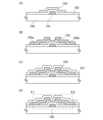
(実施の形態1)
本実施の形態では、図1(D)に示す薄膜トランジスタ150の作製方法の一形態につい
て、薄膜トランジスタ作製工程の断面図である図1(A)乃至図1(D)を用いて説明す
る。薄膜トランジスタ150は、チャネルエッチ型と呼ばれるボトムゲート構造の一つで
ある。(Embodiment 1)
In this embodiment, one embodiment of a method for manufacturing the
まず、絶縁表面を有する基板である基板100上に、フォトマスクを用いてフォトリソグ
ラフィ工程によりゲート電極層101を設ける。なお、レジストマスクをインクジェット
法で形成してもよい。レジストマスクをインクジェット法で形成するとフォトマスクを使
用しないため、製造コストを低減できる。First, a
基板100としては、ガラス基板を用いることが好ましい。基板100として用いるガラ
ス基板は、後の加熱処理の温度が高い場合には、歪み点が730℃以上のものを用いると
良い。また、基板100には、例えば、アルミノシリケートガラス、アルミノホウケイ酸
ガラス、バリウムホウケイ酸ガラスなどのガラス材料が用いられている。なお、酸化ホウ
素(B2O3)と比較して酸化バリウム(BaO)を多く含ませることで、より実用的な
耐熱ガラスが得られる。このため、B2O3よりBaOを多く含むガラス基板を用いるこ
とが好ましい。A glass substrate is preferably used as the
なお、上記の基板100に代えて、セラミック基板、石英ガラス基板、石英基板、サファ
イア基板などの絶縁体でなる基板を用いても良い。他にも、結晶化ガラスなどを用いるこ
とができる。Note that a substrate made of an insulator such as a ceramic substrate, a quartz glass substrate, a quartz substrate, or a sapphire substrate may be used instead of the
また、下地層となる絶縁層を基板100とゲート電極層101の間に設けてもよい。下地
層は、基板100からの不純物元素の拡散を防止する機能があり、窒化珪素、酸化珪素、
窒化酸化珪素、または酸化窒化珪素から選ばれた一または複数の層による積層構造により
形成することができる。Further, an insulating layer serving as a base layer may be provided between the
It can have a stacked-layer structure of one or more layers selected from silicon nitride oxide and silicon oxynitride.
下地層に、塩素、フッ素などのハロゲン元素を含ませることで、基板100からの不純物
元素の拡散を防止する機能をさらに高めることができる。下地層中に含ませるハロゲン元
素の濃度は、SIMS(二次イオン質量分析計)を用いた分析により得られる濃度ピーク
において、1×1015cm3以上1×1020cm3以下とすればよい。By including a halogen element such as chlorine or fluorine in the base layer, the function of preventing impurity elements from diffusing from the
ゲート電極層101としては、金属導電層を用いることができる。金属導電層の材料とし
ては、アルミニウム(Al)、クロム(Cr)、銅(Cu)、タンタル(Ta)、チタン
(Ti)、モリブデン(Mo)、タングステン(W)から選ばれた元素、または上述した
元素を成分とする合金か、上述した元素を組み合わせた合金等を用いるのが好ましい。例
えば、チタン層上にアルミニウム層と、該アルミニウム層上にチタン層が積層された三層
の積層構造、またはモリブデン層上にアルミニウム層と、該アルミニウム層上にモリブデ
ン層を積層した三層の積層構造とすることが好ましい。勿論、金属導電層として単層、ま
たは2層構造、または4層以上の積層構造としてもよい。A metal conductive layer can be used as the
次いで、ゲート電極層101上にゲート絶縁層102を形成する。Next, a
ゲート絶縁層102は、プラズマCVD法またはスパッタリング法等を用いて、酸化珪素
層、窒化珪素層、酸化窒化珪素層または窒化酸化珪素層を単層でまたは積層して形成する
ことができる。例えば、成膜ガスとして、SiH4、酸素及び窒素を用いてプラズマCV
D法により酸化窒化珪素層を形成すればよい。ゲート絶縁層102の厚さは、100nm
以上500nm以下とし、積層の場合は、例えば、厚さ50nm以上200nm以下の第
1のゲート絶縁層と、第1のゲート絶縁層上に厚さ5nm以上300nm以下の第2のゲ
ート絶縁層の積層とする。The
A silicon oxynitride layer may be formed by the D method. The thickness of the
In the case of stacking, for example, a first gate insulating layer with a thickness of 50 nm to 200 nm and a second gate insulating layer with a thickness of 5 nm to 300 nm are stacked over the first gate insulating layer. and
また、酸化物半導体層の形成前に、不活性ガス雰囲気(窒素、またはヘリウム、ネオン、
アルゴン等)下において加熱処理(400℃以上基板の歪み点未満)を行い、層内に含ま
れる水素及び水などの不純物を除去したゲート絶縁層102としてもよい。In addition, an inert gas atmosphere (nitrogen, helium, neon,
The
次いで、ゲート絶縁層102上に、厚さ5nm以上200nm以下、好ましくは10nm
以上50nm以下の酸化物半導体層を形成する。酸化物半導体層の形成後に脱水化または
脱水素化のための加熱処理を行っても酸化物半導体層を非晶質な状態とするため、厚さを
50nm以下と薄くすることが好ましい。酸化物半導体層の厚さを薄くすることで酸化物
半導体層の形成後に加熱処理した場合に、結晶化してしまうのを抑制することができる。Next, a film having a thickness of 5 nm to 200 nm, preferably 10 nm, is formed over the
An oxide semiconductor layer with a thickness greater than or equal to 50 nm and less than or equal to 50 nm is formed. Even if heat treatment for dehydration or dehydrogenation is performed after the oxide semiconductor layer is formed, the oxide semiconductor layer remains amorphous; therefore, the thickness is preferably 50 nm or less. By reducing the thickness of the oxide semiconductor layer, crystallization can be suppressed when heat treatment is performed after the oxide semiconductor layer is formed.
酸化物半導体層は、In-Ga-Zn-O系非単結晶層、In-Sn-Zn-O系、In
-Al-Zn-O系、Sn-Ga-Zn-O系、Al-Ga-Zn-O系、Sn-Al-
Zn-O系、In-Zn-O系、Sn-Zn-O系、Al-Zn-O系、In-Ga-O
系、In-O系、Sn-O系、Zn-O系の酸化物半導体層を用いる。本実施の形態では
、例えば、In-Ga-Zn-O系酸化物半導体ターゲットを用いてスパッタ法により形
成する。また、酸化物半導体層130は、希ガス(代表的にはアルゴン)雰囲気下、酸素
雰囲気下、又は希ガス(代表的にはアルゴン)及び酸素雰囲気下においてスパッタ法によ
り形成することができる。また、スパッタ法を用いる場合、SiO2を2重量%以上10
重量%以下含むターゲットを用いて成膜を行い、酸化物半導体層に結晶化を阻害するSi
Ox(X>0)を含ませ、後の工程で行う脱水化または脱水素化のための加熱処理の際に
結晶化してしまうのを抑制することが好ましい。なお、電源としてパルス直流(DC)電
源を用いると、ごみが軽減でき、厚さ分布も均一となるために好ましい。The oxide semiconductor layer includes an In--Ga--Zn--O-based non-single-crystal layer, an In--Sn--Zn--O-based layer, and an In--Ga--Zn--O-based non-single-crystal layer.
-Al-Zn-O system, Sn-Ga-Zn-O system, Al-Ga-Zn-O system, Sn-Al-
Zn-O system, In-Zn-O system, Sn-Zn-O system, Al-Zn-O system, In-Ga-O
In—O-based, Sn—O-based, or Zn—O-based oxide semiconductor layers are used. In this embodiment, for example, the film is formed by a sputtering method using an In--Ga--Zn--O-based oxide semiconductor target. Further, the oxide semiconductor layer 130 can be formed by a sputtering method in a rare gas (typically argon) atmosphere, an oxygen atmosphere, or an atmosphere of a rare gas (typically argon) and oxygen. Moreover, when using the sputtering method, SiO2 is added to 10% by weight or more.
A film is formed using a target containing less than or equal to 10% by weight of Si, which inhibits crystallization in the oxide semiconductor layer.
It is preferable to contain Ox (X>0) to suppress crystallization during heat treatment for dehydration or dehydrogenation performed in a later step. It is preferable to use a pulse direct current (DC) power supply as the power supply, because dust can be reduced and the thickness distribution can be uniform.
また、酸化物半導体ターゲット中の酸化物半導体の相対密度は80%以上とするのが好ま
しい。これにより、形成された酸化物半導体層中の不純物濃度を低減することができ、電
気特性または信頼性の高い薄膜トランジスタを得ることができる。Further, the relative density of the oxide semiconductor in the oxide semiconductor target is preferably 80% or higher. Accordingly, the impurity concentration in the formed oxide semiconductor layer can be reduced, and a thin film transistor with high electrical characteristics and high reliability can be obtained.
スパッタ法にはスパッタ用電源に高周波電源を用いるRFスパッタ法と、DCスパッタ法
があり、さらにパルス的にバイアスを与えるパルスDCスパッタ法もある。RFスパッタ
法は主に絶縁層を形成する場合に用いられ、DCスパッタ法は主に金属層を形成する場合
に用いられる。The sputtering method includes an RF sputtering method using a high-frequency power source for sputtering, a DC sputtering method, and a pulse DC sputtering method that applies a bias in the form of pulses. The RF sputtering method is mainly used when forming an insulating layer, and the DC sputtering method is mainly used when forming a metal layer.
また、材料の異なるターゲットを複数設置できる多元スパッタ装置もある。多元スパッタ
装置は、同一チャンバーで異なる材料を積層形成することも、同一チャンバーで複数種類
の材料を同時に放電させて形成することもできる。There is also a multi-target sputtering apparatus in which a plurality of targets made of different materials can be installed. The multi-source sputtering apparatus can laminate different materials in the same chamber, or can simultaneously discharge multiple types of materials in the same chamber.
また、チャンバー内部に磁石機構を備えたマグネトロンスパッタ法を用いるスパッタ装置
や、グロー放電を使わずマイクロ波を用いて発生させたプラズマを用いるECRスパッタ
法を用いるスパッタ装置がある。There are also sputtering apparatuses that use a magnetron sputtering method that has a magnet mechanism inside a chamber, and sputtering apparatuses that use an ECR sputtering method that uses plasma generated using microwaves without using glow discharge.
また、スパッタ法を用いる成膜方法として、成膜中にターゲット物質とスパッタガス成分
とを化学反応させてそれらの化合物薄膜を形成するリアクティブスパッタ法や、成膜中に
基板にも電圧をかけるバイアススパッタ法もある。In addition, as a film formation method using a sputtering method, there is a reactive sputtering method in which a target material and a sputtering gas component are chemically reacted during film formation to form a compound thin film, and a voltage is applied to a substrate during film formation. There is also a bias sputtering method.
また、酸化物半導体膜の成膜を行う前に、スパッタ装置内壁や、ターゲット表面やターゲ
ット材料中に残存している水分または水素を除去するためにプレヒート処理を行うと良い
。プレヒート処理としては成膜チャンバー内を減圧下で200℃~600℃に加熱する方
法や、加熱しながら窒素や不活性ガスの導入と排気を繰り返す方法等がある。この場合の
ターゲット冷却液は、水ではなく油脂等を用いるとよい。加熱せずに窒素の導入と排気を
繰り返しても一定の効果が得られるが、加熱しながら行うとなお良い。プレヒート処理を
終えたら、基板またはスパッタ装置を冷却し、酸化物半導体膜の成膜を行う。In addition, preheat treatment is preferably performed to remove moisture or hydrogen remaining in the inner wall of the sputtering apparatus, the surface of the target, or the target material before the oxide semiconductor film is formed. As the preheating process, there is a method of heating the inside of the film forming chamber to 200° C. to 600° C. under reduced pressure, a method of repeatedly introducing and exhausting nitrogen or an inert gas while heating, and the like. In this case, it is preferable to use oil or the like instead of water as the target cooling liquid. A certain effect can be obtained by repeating the introduction and evacuation of nitrogen without heating, but it is more preferable to carry out while heating. After the preheating treatment, the substrate or the sputtering apparatus is cooled, and an oxide semiconductor film is formed.
また、スパッタ法による成膜中に基板を400℃以上700以下に加熱してもよい。Further, the substrate may be heated to 400° C. or more and 700° C. or less during film formation by sputtering.
また、酸化物半導体膜の成膜を行う前、または成膜中、または成膜後に、スパッタ装置内
をクライオポンプを用いて中に残存している水分などを除去することが好ましい。Further, before, during, or after the formation of the oxide semiconductor film, it is preferable to remove remaining moisture or the like from the inside of the sputtering apparatus using a cryopump.
また、ゲート絶縁層102、及び酸化物半導体膜を大気に触れさせることなく連続的に形
成してもよい。大気に触れさせることなく形成することで、界面が、水やハイドロカーボ
ンなどの、大気成分や大気中に浮遊する不純物元素に汚染されることなく各積層界面を形
成することができるので、薄膜トランジスタ特性のばらつきを低減することができる。Alternatively, the
次いで、酸化物半導体層をフォトリソグラフィ工程により島状の酸化物半導体層103に
加工する(図1(A)参照。)。また、島状の酸化物半導体層103を形成するためのレ
ジストマスクをインクジェット法で形成してもよい。レジストマスクをインクジェット法
で形成するとフォトマスクを使用しないため、製造コストを低減できる。Next, the oxide semiconductor layer is processed into an island-shaped
次いで、第1の熱処理を行って、酸化物半導体層103の脱水化または脱水素化を行う。
脱水化または脱水素化を行う第1の熱処理の温度は、処理中の最高温度が350℃以上7
50℃以下、好ましくは425℃以上とする。なお、425℃以上であれば熱処理時間は
1時間以下でよいが、425℃未満であれば加熱処理時間は、1時間よりも長時間行うこ
ととする。例えば、加熱処理装置の一つである電気炉に基板を導入し、酸化物半導体層に
対して窒素雰囲気下において加熱処理を行った後、大気に触れることなく、酸化物半導体
層への水や水素の再混入を防ぎ、酸化物半導体層103を得ることができる。本実施の形
態では、酸化物半導体層103の脱水化または脱水素化を行う加熱温度Tから、再び水が
入らないような十分な温度まで同じ炉を用い、具体的には加熱温度Tよりも100℃以上
下がるまで窒素雰囲気下で徐冷する。また、窒素雰囲気に限定されず、ヘリウム、ネオン
、アルゴン等の希ガス下において脱水化または脱水素化を行う。Next, first heat treatment is performed to dehydrate or dehydrogenate the
The temperature of the first heat treatment for dehydration or dehydrogenation has a maximum temperature of 350° C. or higher during the treatment.
50° C. or lower, preferably 425° C. or higher. Note that when the temperature is 425° C. or higher, the heat treatment time may be one hour or less, but when the temperature is lower than 425° C., the heat treatment time is longer than one hour. For example, the substrate is introduced into an electric furnace, which is one of the heat treatment apparatuses, and the oxide semiconductor layer is subjected to heat treatment in a nitrogen atmosphere. The
第1の熱処理により酸化物半導体層103を構成する酸化物半導体の原子レベルの再配列
が行われる。第1の熱処理は、酸化物半導体層103中におけるキャリアの移動を阻害す
る歪みを解放できる点で重要である。By the first heat treatment, rearrangement at the atomic level of the oxide semiconductor forming the
なお、第1の熱処理においては、窒素、またはヘリウム、ネオン、アルゴン等の希ガスに
、水、水素などが含まれないことが好ましい。または、加熱処理装置に導入する窒素、ま
たはヘリウム、ネオン、アルゴン等の希ガスの純度を、6N(99.9999%)以上、
好ましくは7N(99.99999%)以上、(即ち不純物濃度を1ppm以下、好まし
くは0.1ppm以下)とすることが好ましい。Note that in the first heat treatment, nitrogen or a rare gas such as helium, neon, or argon preferably does not contain water, hydrogen, or the like. Alternatively, the purity of nitrogen or rare gases such as helium, neon, and argon to be introduced into the heat treatment apparatus is 6N (99.9999%) or more,
It is preferably 7N (99.99999%) or more (that is, the impurity concentration is 1 ppm or less, preferably 0.1 ppm or less).
また、第1の熱処理は、電気炉を用いた加熱方法を用いることができる。なお、第1の熱
処理は、加熱処理装置は電気炉に限られず、抵抗発熱体などの発熱体からの熱伝導または
熱輻射によって、被処理物を加熱する装置を備えていてもよい。例えば、GRTA(Ga
s Rapid Thermal Anneal)装置、LRTA(Lamp Rapi
d Thermal Anneal)装置等のRTA(Rapid Thermal A
nneal)装置を用いることができる。LRTA装置は、ハロゲンランプ、メタルハラ
イドランプ、キセノンアークランプ、カーボンアークランプ、高圧ナトリウムランプ、高
圧水銀ランプなどのランプから発する光(電磁波)の輻射により、被処理物を加熱する装
置である。GRTA装置は、高温のガスを用いて加熱処理を行う装置である。気体には、
アルゴンなどの希ガス、または窒素のような、加熱処理によって被処理物と反応しない不
活性気体が用いられる。A heating method using an electric furnace can be used for the first heat treatment. In the first heat treatment, the heat treatment apparatus is not limited to an electric furnace, and may be provided with a device that heats the object by heat conduction or heat radiation from a heating element such as a resistance heating element. For example, GRTA(Ga
s Rapid Thermal Anneal) device, LRTA (Lamp Rapi
RTA (Rapid Thermal A, such as d Thermal Anneal) equipment
nneal) device can be used. An LRTA apparatus is an apparatus that heats an object by radiation of light (electromagnetic waves) emitted from lamps such as halogen lamps, metal halide lamps, xenon arc lamps, carbon arc lamps, high pressure sodium lamps, and high pressure mercury lamps. The GRTA apparatus is an apparatus that performs heat treatment using high-temperature gas. For gases,
A rare gas such as argon or an inert gas such as nitrogen that does not react with the object to be processed by heat treatment is used.
また、第1の熱処理の条件、または酸化物半導体層の材料によっては、酸化物半導体層が
結晶化し、微結晶層または多結晶層となる場合もある。ここで、酸化物半導体層は、結晶
化率が80%以上または90%以上の微結晶層となることがある。また、酸化物半導体層
の材料によっては、結晶を有さない酸化物半導体層となることもある。Further, depending on the conditions of the first heat treatment or the material of the oxide semiconductor layer, the oxide semiconductor layer might be crystallized to be a microcrystalline layer or a polycrystalline layer. Here, the oxide semiconductor layer may be a microcrystalline layer with a crystallization rate of 80% or more or 90% or more. Further, depending on the material of the oxide semiconductor layer, the oxide semiconductor layer may be a crystalless oxide semiconductor layer.
また、酸化物半導体層の第1の熱処理は、島状の酸化物半導体層103に加工する前の酸
化物半導体層に行うこともできる。その場合には、第1の熱処理後に、加熱装置から基板
を取り出し、フォトリソグラフィ工程を行う。Alternatively, the first heat treatment of the oxide semiconductor layer can be performed on the oxide semiconductor layer before being processed into the island-shaped
ここで、酸化物半導体層中の脱水素化有無における、水素濃度分析結果について触れてお
く。図4(A)は、本分析で用いた試料の断面構造模式図である。ガラス基板400上に
プラズマCVD法で酸化窒化絶縁層401を形成し、酸化窒化絶縁層401上にIn-G
a-Zn-O系酸化物半導体層402を約40nm形成したものを用意した。用意した試
料を分断し、一つは脱水素化を行わず、もう一つはGRTA法による窒素雰囲気中650
℃、6分間の脱水素化を行なった。それぞれの試料について、酸化物半導体層中の水素濃
度を測定することで、熱処理による脱水素化の効果について調査した。Here, the results of hydrogen concentration analysis in the presence or absence of dehydrogenation in the oxide semiconductor layer will be described. FIG. 4A is a schematic diagram of the cross-sectional structure of the sample used in this analysis. An
An a-Zn-O-based
°C for 6 minutes. The effect of dehydrogenation by heat treatment was investigated by measuring the hydrogen concentration in the oxide semiconductor layer of each sample.
酸化物半導体層中の水素濃度測定は、二次イオン質量分析法(SIMS:Seconda
ry Ion Mass Spectroscopy)で行った。図4(B)は、酸化物
半導体層中の厚さ方向の水素濃度分布を示すSIMS分析結果である。横軸は試料表面か
らの深さを示しており、左端の深さ0nmの位置が試料最表面(酸化物半導体層の最表面
)に相当する。図4(A)に示す分析方向403は、SIMS分析の分析方向を示してい
る。分析は酸化物半導体層の最表面からガラス基板400に向かう方向で行った。つまり
、図4(B)の横軸において、左端から右端の方向に向かって行った。図4(B)の縦軸
は、特定深さにおける試料中の水素濃度と、酸素イオン強度を対数軸で示している。Hydrogen concentration measurement in the oxide semiconductor layer is performed by secondary ion mass spectrometry (SIMS: Seconda
ry Ion Mass Spectroscopy). FIG. 4B shows SIMS analysis results showing the hydrogen concentration distribution in the thickness direction of the oxide semiconductor layer. The horizontal axis indicates the depth from the surface of the sample, and the leftmost position at a depth of 0 nm corresponds to the outermost surface of the sample (the outermost surface of the oxide semiconductor layer). An
図4(B)において、水素濃度プロファイル412は、脱水素化を行っていない酸化物半
導体層中の水素濃度プロファイルを示しており、水素濃度プロファイル413は、熱処理
による脱水素化を行った後の酸化物半導体層中の水素濃度プロファイルを示している。酸
素イオン強度プロファイル411は、水素濃度プロファイル412測定時に同時に取得し
た酸素イオン強度を示している。酸素イオン強度プロファイル411に極端な変動が無く
、ほぼ一定のイオン強度が得られていることから、SIMS分析が正確に行われているこ
とがわかる。なお、図示していないが、水素濃度プロファイル413測定時も同様に酸素
イオン強度を測定しており、こちらもほぼ一定のイオン強度が得られている。水素濃度プ
ロファイル412及び水素濃度プロファイル413は、試料と同じIn-Ga-Zn-O
系酸化物半導体層で作製した標準試料を用いて定量している。In FIG. 4B, a
It is quantified using a standard sample made of a base oxide semiconductor layer.
なお、SIMS分析は、その原理上、試料表面近傍や、材質が異なる層の積層界面近傍の
データを正確に得ることが困難であることが知られている。本分析においては、試料最表
面から深さ約15nmまでは正確なデータが得られていないと考えられるため、深さ15
nm以降のプロファイルを評価した。In SIMS analysis, it is known that, due to its principle, it is difficult to obtain accurate data in the vicinity of the sample surface or in the vicinity of the lamination interface of layers of different materials. In this analysis, it is thought that accurate data is not obtained from the top surface of the sample to a depth of about 15 nm, so a depth of 15 nm
The profile after nm was evaluated.
水素濃度プロファイル412から、脱水素化を行っていない酸化物半導体層中に、水素が
約3×10²⁰atoms/cm3以上、約5×1020atoms/cm3以下、平均
水素濃度で約4×10²⁰atoms/cm3含まれていることがわかる。また、水素濃
度プロファイル413から、脱水素化により、酸化物半導体層中の平均水素濃度を約2×
1019atoms/cm3に低減できていることがわかる。From the
It can be seen that it can be reduced to 1019 atoms/cm3 .
本分析により、熱処理による脱水素化を行うことで、酸化物半導体層中の水素濃度を低減
できることが確認できた。また、GRTA法による窒素雰囲気中650℃、6分間の脱水
素化により、酸化物半導体層中の水素濃度を1/10以下に低減できることが確認できた
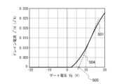
。From this analysis, it was confirmed that the hydrogen concentration in the oxide semiconductor layer can be reduced by performing dehydrogenation by heat treatment. Further, it was confirmed that the hydrogen concentration in the oxide semiconductor layer could be reduced to 1/10 or less by dehydrogenation in a nitrogen atmosphere at 650° C. for 6 minutes by the GRTA method.
また、図4に示したSIMS分析時に同時に測定した、酸化物半導体層中のH+Oイオン
強度と、H2+Oイオン強度の検出結果を図5に示す。図5(A1)は、脱水素化を行っ
ていない酸化物半導体層中のH+Oイオン強度であり、図5(A2)は、脱水素化を行っ
た酸化物半導体層中のH+Oイオン強度である。また、図5(B1)は、脱水素化を行っ
ていない酸化物半導体層中のH2+Oイオン強度であり、図5(B2)は、脱水素化を行
った酸化物半導体層中のH2+Oイオン強度である。どちらも脱水素化した試料の方がイ
オン強度が小さくなっており、GRTA法で650℃、6分間の加熱処理により、水分ま
たはOHの脱離が効率よく行われていることがわかる。FIG. 5 shows detection results of the H+O ion intensity and the H2 +O ion intensity in the oxide semiconductor layer, which were measured at the same time as the SIMS analysis shown in FIG. FIG. 5A1 shows the H + O ion intensity in the oxide semiconductor layer that has not been dehydrogenated, and FIG. 5A2 shows the H + O ion intensity in the oxide semiconductor layer that has been dehydrogenated. . Further, FIG. 5B1 shows the
つづいて、In-Ga-Zn-O系酸化物半導体から水分子が脱離する機構について、計
算化学により解析した結果を図6を用いて説明する。本解析は、量子化学計算プログラム
Gaussian03を用いて行った。酸化物半導体中では水分子だけでなく、OHがH
と化合し水分子として脱離する可能性があるため、酸化物半導体中に存在しているOH基
の脱離機構について解析を行った。Next, results of computational chemistry analysis of a mechanism of desorption of water molecules from an In--Ga--Zn--O-based oxide semiconductor will be described with reference to FIG. This analysis was performed using the quantum chemical calculation program Gaussian03. In oxide semiconductors, not only water molecules but also OH
and there is a possibility of desorption as water molecules, the desorption mechanism of the OH group present in the oxide semiconductor was analyzed.
図6(A)は、OH基を含む酸化物半導体中の最安定構造の始状態を示しており、図6(
D)はOH基が水分子(H2O分子)となって無限遠に脱離した終状態を示している。図
6(B)及び図6(C)は、図6(A)から図6(D)に至るまでの遷移状態及び中間状
態を示す図である。M1、M2、M’は金属原子を表しており、In、Ga、Znを想定
している。つまり、M1-M2の全組み合わせは、In-In、Ga-Ga、Zn-Zn
、In-Ga、In-Zn、Ga-Znの6通りが存在する。なお、本計算ではM’を水
素原子に置き換えて、最小分子構造単位での計算を行った。以下、OH基の脱離メカニズ
ムについて順を追って説明する。FIG. 6A shows the initial state of the most stable structure in an oxide semiconductor containing OH groups, and FIG.
D) shows the final state in which the OH group becomes a water molecule (H2 O molecule) and is infinitely detached. 6(B) and 6(C) are diagrams showing transition states and intermediate states from FIG. 6(A) to FIG. 6(D). M1 , M2 , and M′ represent metal atoms, which are assumed to be In, Ga, and Zn. That is, all combinations of M1 -M2 are In-In, Ga-Ga, Zn-Zn
, In—Ga, In—Zn, and Ga—Zn. In addition, in this calculation, M′ was replaced with a hydrogen atom, and the calculation was performed in the minimum molecular structural unit. The OH group detachment mechanism will be described in order below.
まず、始状態において、OH基701がM1と結合し、OH基702がM1とM2を架橋
するように配位結合を形成している(図6(A)参照)。First, in the initial state, an
次に、一定以上のエネルギーが酸化物半導体に加えられると、OH基702のHが、OH
基701へ転位し(図6(B)参照)、H2O分子705を生成する。H2O分子705
は、M1と配位結合を形成する(図6(C)参照)。最後に、H2O分子705は、M1
から無限遠に脱離したH2O分子710となる(図6(D)参照)。Next, when energy above a certain level is applied to the oxide semiconductor, H of the
It rearranges to group 701 (see FIG. 6B) to generate H2 O molecule 705 .H2O
forms a coordinate bond withM1 (see FIG. 6(C)). Finally, the H2 O molecule 705 is M1
becomes H2 O molecules 710 that are infinitely detached from the (see FIG. 6(D)).
図6(E)は、M1-M2をIn-Gaとした時の、図6(A)乃至図6(D)の各状態
におけるポテンシャルエネルギーの値を示している。エネルギー711は、図6(A)に
示す状態の時のエネルギーを示している。エネルギー712は、図6(B)に示す状態の
時のエネルギーを示している。エネルギー713は、図6(C)に示す状態の時のエネル
ギーを示している。エネルギー714は図6(D)に示す状態の時のエネルギーを示して
いる。FIG. 6(E) shows potential energy values in the respective states of FIGS. 6(A) to 6(D) when M1 -M2 are In—Ga.
本解析結果から、M1-M2がIn-Gaの時の、水分子生成の活性化エネルギーは1.
14eVであることがわかった。図6(F)に、M1-M2の6つの組み合わせにおける
水生成反応の活性化エネルギー(Ea)の計算結果を示す。M1-M2の6つの組み合わ
せの中で、M1-M2がIn-Gaの時の活性化エネルギーが最も小さく、Zn-Znの
時の活性化エネルギーが最も大きい事がわかった。また、M1-M2の組み合わせにZn
が含まれると、活性化エネルギーが大きくなる傾向がみられるため、In-Ga-Zn-
O系酸化物半導体においては、ZnがOH基脱離の阻害要因となっている可能性が推測さ
れる。From the results of this analysis, the activation energy of water molecule generation when M1 -M2 is In—Ga is 1.
It was found to be 14 eV. FIG. 6(F) shows the calculation results of the activation energies (Ea) of the water-producing reactions in the six combinations of M1 -M2 . It was found that among the six combinations of M1 -M2 , the activation energy is the lowest when M1 -M2 is In—Ga and the highest when M 1 -
is included, the activation energy tends to increase, so In—Ga—Zn—
In the O-based oxide semiconductor, Zn is presumed to be a factor that inhibits elimination of OH groups.
本解析結果から、In-Ga-Zn-O系酸化物半導体において、熱処理によるOH基の
脱離を効率よく行うには、InとGaの含有量(原子数)が同程度、もしくはInがGa
より多い方が好ましい事がわかった。また、Znの含有量(原子数)が、InとGaを合
わせた含有量よりも少ない事が好ましく、さらに、InとGaそれぞれの含有量よりも少
ない事がより好ましいことがわかった。From the results of this analysis, in order to efficiently desorb OH groups by heat treatment in an In—Ga—Zn—O-based oxide semiconductor, the contents (number of atoms) of In and Ga should be about the same, or In should be equal to Ga
It turns out that more is better. In addition, it was found that the content of Zn (the number of atoms) is preferably less than the total content of In and Ga, and more preferably less than the content of In and Ga.
酸化物半導体の組成を最適化することで、熱処理による脱水化または脱水素化を効率よく
行うことができる。By optimizing the composition of the oxide semiconductor, dehydration or dehydrogenation by heat treatment can be efficiently performed.
次いで、ゲート絶縁層102、及び酸化物半導体層103上にソース電極層及びドレイン
電極層を形成するための導電層を形成する。Next, a conductive layer for forming a source electrode layer and a drain electrode layer is formed over the
ソース電極層及びドレイン電極層を形成するための導電層としては、ゲート電極層101
と同様に、金属導電層を用いることができる。金属導電層の材料としては、Al、Cr、
Cu、Ta、Ti、Mo、Wから選ばれた元素、または上述した元素を成分とする合金か
、上述した元素を組み合わせた合金等を用いるのが好ましい。例えば、チタン層上にアル
ミニウム層と、該アルミニウム層上にチタン層が積層された三層の積層構造、またはモリ
ブデン層上にアルミニウム層と、該アルミニウム層上にモリブデン層を積層した三層の積
層構造とすることが好ましい。勿論、金属導電層として単層、または2層構造、または4
層以上の積層構造としてもよい。As a conductive layer for forming the source electrode layer and the drain electrode layer, the
Similarly, a metal conductive layer can be used. Materials for the metal conductive layer include Al, Cr,
It is preferable to use an element selected from Cu, Ta, Ti, Mo and W, an alloy containing the above elements, or an alloy combining the above elements. For example, a three-layer laminate structure in which an aluminum layer is laminated on a titanium layer and a titanium layer is laminated on the aluminum layer, or a three-layer laminate structure in which an aluminum layer is laminated on a molybdenum layer and a molybdenum layer is laminated on the aluminum layer A structure is preferred. Of course, a single layer, a two-layer structure, or a four-layer structure as the metal conductive layer
A laminated structure of more than one layer may be used.
フォトマスクを用いてフォトリソグラフィ工程により、ソース電極層及びドレイン電極層
を形成するための導電層から、ソース電極層105aまたはドレイン電極層105bを形
成する(図1(B)参照。)。また、このとき酸化物半導体層103も一部がエッチング
され、溝部(凹部)を有する酸化物半導体層103となる。A
なお、ソース電極層105aまたはドレイン電極層105bを形成するためのレジストマ
スクをインクジェット法で形成してもよい。レジストマスクをインクジェット法で形成す
るとフォトマスクを使用しないため、製造コストを低減できる。Note that a resist mask for forming the
また、酸化物半導体層103と、ソース電極層105aまたはドレイン電極層105bの
間に、酸化物半導体層103よりも抵抗が低い酸化物導電層を形成しても良い。このよう
な積層構成とすることで、薄膜トランジスタの耐圧を向上させることができる。具体的に
は、抵抗が低い酸化物導電層のキャリア濃度は、例えば1×10²⁰/cm3以上1×1
021/cm3以下の範囲内であると好ましい。Alternatively, an oxide conductive layer having lower resistance than the
It is preferably in the range of 021 /cm3 or less.
次に、ゲート絶縁層102、酸化物半導体層103、ソース電極層105a及びドレイン
電極層105bを覆い、酸化物半導体層103の一部と接する絶縁層107を形成する(
図1(C)参照。)。絶縁層107は、少なくとも1nm以上の厚さとし、CVD法、ス
パッタリング法など、絶縁層107に水、水素等の不純物を混入させない方法を適宜用い
て形成することができる。ここでは、絶縁層107は、例えばスパッタリング法の一種で
ある、リアクティブスパッタリング法を用いて形成する。酸化物半導体層103の一部と
接して形成される絶縁層107は、水分や、水素イオンや、OH-などの不純物を含まず
、これらが外部から侵入することをブロックする無機絶縁層を用い、代表的には酸化珪素
層、窒化酸化珪素層、窒化珪素層、酸化アルミニウム層、酸化窒化アルミニウム層又は窒
化アルミニウム層、を用いることができる。Next, an insulating
See FIG. 1(C). ). The insulating
また、絶縁層107は、酸化珪素層、窒化酸化珪素層、酸化アルミニウム層又は酸化窒化
アルミニウム層の上に窒化珪素層又は窒化アルミニウム層を積層する構造としてもよい。
特に窒化珪素層は水分や、水素イオンや、OH-などの不純物を含まず、これらが外部か
ら侵入することをブロックしやすいので好ましい。Alternatively, the insulating
In particular, the silicon nitride layer is preferable because it does not contain impurities such as moisture, hydrogen ions, andOH .
絶縁層107の形成時の基板温度は、室温以上300℃以下とすればよく、酸化珪素層の
スパッタリング法による成膜は、希ガス(代表的にはアルゴン)雰囲気下、酸素雰囲気下
、または希ガス(代表的にはアルゴン)及び酸素雰囲気下において行うことができる。ま
た、ターゲットとして酸化珪素ターゲットまたは珪素ターゲットを用いることができる。
例えば、珪素ターゲットを用いて、酸素及び希ガス雰囲気下でスパッタリング法により酸
化珪素を形成することができる。The substrate temperature at which the insulating
For example, using a silicon target, silicon oxide can be formed by a sputtering method in an atmosphere of oxygen and a rare gas.
次いで、第2の熱処理を行う。第2の熱処理は、100℃以上、第1の熱処理における処
理中の最高温度以下で行う。例えば、加熱処理装置の一つである電気炉に基板を導入し、
窒素雰囲気下において加熱処理を行う。第2の熱処理は、絶縁層107形成以降の工程で
あれば、いつ行ってもよい。Then, a second heat treatment is performed. The second heat treatment is performed at a temperature of 100° C. or higher and not higher than the highest temperature during treatment in the first heat treatment. For example, the substrate is introduced into an electric furnace, which is one of the heat treatment devices,
Heat treatment is performed in a nitrogen atmosphere. The second heat treatment may be performed at any time after the insulating
以上の工程より、絶縁表面を有する基板である基板100上にゲート電極層101が設け
られ、ゲート電極層101の上にゲート絶縁層102が設けられ、ゲート絶縁層102の
上に酸化物半導体層103が設けられ、酸化物半導体層103の上にソース電極層105
aまたはドレイン電極層105bが設けられ、ゲート絶縁層102、酸化物半導体層10
3、ソース電極層105a及びドレイン電極層105bを覆い、酸化物半導体層103の
一部と接する絶縁層107が設けられている、チャネルエッチ型の薄膜トランジスタ15
0を形成することができる(図1(D)参照。)。Through the above steps, the
a or the
3. A channel-etched
0 can be formed (see FIG. 1D).
図2は、本実施の形態で示した薄膜トランジスタ150の上面図である。図1(D)は、
図2のX1-X2部位の断面構成を示している。図2において、Lはチャネル長を示して
おり、Wはチャネル幅を示している。また、Aはチャネル幅方向と平行な方向において、
酸化物半導体層103がソース電極層105a及びドレイン電極層105bと重ならない
領域の長さを示している。Lsはソース電極層105aとゲート電極層101が重なる長
さを示しており、Ldはドレイン電極層105bとゲート電極層101が重なる長さを示
している。FIG. 2 is a top view of the
3 shows a cross-sectional configuration of the X1-X2 portion of FIG. 2; In FIG. 2, L indicates the channel length and W indicates the channel width. In addition, in the direction parallel to the channel width direction, A is
The length of the region where the
本実施の形態では、薄膜トランジスタ150をシングルゲート構造の薄膜トランジスタを
用いて説明したが、必要に応じて、チャネル形成領域を複数有するマルチゲート構造の薄
膜トランジスタや、絶縁層107上に第2のゲート電極層を有する構造の薄膜トランジス
タとすることもできる。In this embodiment mode, a thin film transistor with a single-gate structure is used as the
また、本実施の形態では、チャネルエッチ型の薄膜トランジスタ150の作製方法につい
て説明したが、本実施の形態の構成はこれに限られるものではない。図3(A)に示すよ
うな、ボトムゲート構造の薄膜トランジスタ160(逆コプラナ型とも呼ぶ)や、図3(
B)に示すような、チャネル保護層110を有するチャネル保護型(チャネルストップ型
ともいう)の薄膜トランジスタ170等も同様の材料、方法を用いて形成することができ
る。図3(C)は、チャネルエッチ型薄膜トランジスタの他の例を示している。図3(C
)に示す薄膜トランジスタ180は、ゲート電極層101が酸化物半導体層103の端部
よりも外側に伸びた構造となっている。In addition, although the method for manufacturing the channel-etched
A channel protective (also referred to as a channel stop)
) has a structure in which the
なお、薄膜トランジスタのチャネル長(図2中のL)は、ソース電極層105aとドレイ
ン電極層105bとの距離で定義されるが、チャネル保護型の薄膜トランジスタのチャネ
ル長は、キャリアの流れる方向と平行な方向のチャネル保護層の幅で定義される。Note that the channel length of the thin film transistor (L in FIG. 2) is defined by the distance between the
本実施の形態により、酸化物半導体をチャネル形成領域として用いる薄膜トランジスタの
しきい値電圧を0Vに近づけることができる。According to this embodiment, the threshold voltage of a thin film transistor in which an oxide semiconductor is used as a channel formation region can be brought close to 0V.
また、処理温度150℃、処理時間1時間、電界強度2×10⁶V/cmの条件における
BT試験において、BT試験前後でのしきい値電圧の変化量が2V以下、好ましくは1.
5V以下、さらに好ましくは1.0V以下である酸化物半導体層を有する薄膜トランジス
タを作製することができる。In addition, in a BT test under conditions of a treatment temperature of 150° C., a treatment time of 1 hour, and an electric field strength of 2×10⁶ V/cm, the amount of change in threshold voltage before and after the BT test is 2 V or less, preferably 1.
A thin film transistor having an oxide semiconductor layer with a voltage of 5 V or lower, preferably 1.0 V or lower can be manufactured.
本実施の形態は、他の実施の形態に記載した構成と適宜組み合わせて実施することが可能
である。This embodiment can be implemented in appropriate combination with any structure described in any of the other embodiments.
(実施の形態2)
本実施の形態では、同一基板上に少なくとも駆動回路の一部と、画素部に配置する薄膜ト
ランジスタを作製する例について以下に説明する。(Embodiment 2)
In this embodiment mode, an example in which at least part of a driver circuit and a thin film transistor provided in a pixel portion are manufactured over the same substrate will be described below.
画素部に配置する薄膜トランジスタは、実施の形態1に従って形成する。また、実施の形
態1に示す薄膜トランジスタはnチャネル型TFTであるため、駆動回路のうち、nチャ
ネル型TFTで構成することができる駆動回路の一部を画素部の薄膜トランジスタと同一
基板上に形成する。A thin film transistor arranged in a pixel portion is formed according to
アクティブマトリクス型表示装置のブロック図の一例を図7(A)に示す。表示装置の基
板5300上には、画素部5301、第1の走査線駆動回路5302、第2の走査線駆動
回路5303、信号線駆動回路5304を有する。画素部5301には、複数の信号線が
信号線駆動回路5304から延伸して配置され、複数の走査線が第1の走査線駆動回路5
302、及び第2の走査線駆動回路5303から延伸して配置されている。なお走査線と
信号線との交差領域には、各々、表示素子を有する画素がマトリクス状に配置されている
。また、表示装置の基板5300はFPC(Flexible Printed Cir
cuit)等の接続部を介して、タイミング制御回路5305(コントローラ、制御IC
ともいう)に接続されている。An example of a block diagram of an active matrix display device is shown in FIG. A
302 and the second scanning
timing control circuit 5305 (controller, control IC
) is connected.
図7(A)では、第1の走査線駆動回路5302、第2の走査線駆動回路5303、信号
線駆動回路5304は、画素部5301と同じ基板5300上に形成される。そのため、
外部に設ける駆動回路等の部品の数が減るので、コストの低減を図ることができる。また
、基板5300外部に駆動回路を設けた場合の配線を延伸させることによる接続部での接
続数を減らすことができ、信頼性の向上、又は歩留まりの向上を図ることができる。In FIG. 7A, the first scan
Since the number of parts such as drive circuits provided outside is reduced, the cost can be reduced. In addition, the number of connections in connection portions can be reduced by extending wiring when a driver circuit is provided outside the
なお、タイミング制御回路5305は、第1の走査線駆動回路5302に対し、一例とし
て、第1の走査線駆動回路用スタート信号(GSP1)(スタートパルスともいう)、走
査線駆動回路用クロック信号(GCK1)を供給する。また、タイミング制御回路530
5は、第2の走査線駆動回路5302に対し、一例として、第2の走査線駆動回路用スタ
ート信号(GSP2)、走査線駆動回路用クロック信号(GCK2)を供給する。またタ
イミング制御回路5305は、信号線駆動回路5304に、信号線駆動回路用スタート信
号(SSP)、信号線駆動回路用クロック信号(SCK)、ビデオ信号用データ(DAT
A)(単にビデオ信号ともいう)、ラッチ信号(LAT)を供給するものとする。なお各
クロック信号は、周期のずれた複数のクロック信号でもよいし、クロック信号を反転させ
た信号(CKB)とともに供給されるものであってもよい。なお、第1の走査線駆動回路
5302と第2の走査線駆動回路5303との一方を省略することが可能である。Note that the
5 supplies the second scanning
A) (also simply referred to as a video signal) shall provide a latch signal (LAT). Note that each clock signal may be a plurality of clock signals with different cycles, or may be supplied together with a signal (CKB) obtained by inverting the clock signal. Note that one of the first scanning
図7(B)では、駆動周波数が低い回路(例えば、第1の走査線駆動回路5302、第2
の走査線駆動回路5303)を画素部5301と同じ基板5300に形成し、信号線駆動
回路5304を画素部5301とは別の基板に形成する構成について示している。当該構
成により、単結晶半導体を用いたトランジスタと比較すると電界効果移動度が小さい薄膜
トランジスタによって、基板5300に形成する駆動回路を構成することができる。した
がって、表示装置の大型化、工程数の削減、コストの低減、又は歩留まりの向上などを図
ることができる。In FIG. 7B, circuits with low driving frequencies (for example, the first scanning
A scanning line driver circuit 5303) is formed on the
また、実施の形態1に示す薄膜トランジスタは、nチャネル型TFTである。図8(A)
、図8(B)ではnチャネル型TFTで構成する信号線駆動回路の構成、動作について一
例を示し説明する。Further, the thin film transistor described in
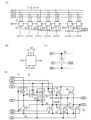
FIG. 8B shows an example of the configuration and operation of a signal line driver circuit composed of n-channel TFTs.
信号線駆動回路は、シフトレジスタ5601、及びスイッチング回路5602を有する。
スイッチング回路5602は、スイッチング回路5602_1~5602_N(Nは自然
数)という複数の回路を有する。スイッチング回路5602_1~5602_Nは、各々
、薄膜トランジスタ5603_1~5603_k(kは自然数)という複数のトランジス
タを有する。薄膜トランジスタ5603_1~5603_kは、Nチャネル型TFTであ
る例を説明する。The signal line driver circuit has a
The
信号線駆動回路の接続関係について、スイッチング回路5602_1を例にして説明する
。薄膜トランジスタ5603_1~5603_kの第1端子は、各々、配線5604_1
~5604_kと接続される。薄膜トランジスタ5603_1~5603_kの第2端子
は、各々、信号線S1~Skと接続される。薄膜トランジスタ5603_1~5603_
kのゲートは、配線5605_1と接続される。The connection relationship of the signal line driver circuit will be described using the switching circuit 5602_1 as an example. First terminals of the thin film transistors 5603_1 to 5603_k are each connected to a wiring 5604_1.
~5604_k. Second terminals of the thin film transistors 5603_1 to 5603_k are connected to the signal lines S1 to Sk, respectively. Thin film transistors 5603_1 to 5603_
The gate of k is connected to the wiring 5605_1.
シフトレジスタ5601は、配線5605_1~5605_Nに順番にHレベル(H信号
、高電源電位レベル、ともいう)の信号を出力し、スイッチング回路5602_1~56
02_Nを順番に選択する機能を有する。The
02_N in order.
スイッチング回路5602_1は、配線5604_1~5604_kと信号線S1~Sk
との導通状態(第1端子と第2端子との間の導通)を制御する機能、即ち配線5604_
1~5604_kの電位を信号線S1~Skに供給するか否かを制御する機能を有する。
このように、スイッチング回路5602_1は、セレクタとしての機能を有する。また薄
膜トランジスタ5603_1~5603_kは、各々、配線5604_1~5604_k
と信号線S1~Skとの導通状態を制御する機能、即ち配線5604_1~5604_k
の電位を信号線S1~Skに供給する機能を有する。このように、薄膜トランジスタ56
03_1~5603_kは、各々、スイッチとしての機能を有する。The switching circuit 5602_1 includes wirings 5604_1 to 5604_k and signal lines S1 to Sk.
(conductivity between the first terminal and the second terminal), that is, the wiring 5604_
It has a function of controlling whether or not the potentials of 1 to 5604_k are supplied to the signal lines S1 to Sk.
Thus, the switching circuit 5602_1 functions as a selector. Thin film transistors 5603_1 to 5603_k are connected to wirings 5604_1 to 5604_k, respectively.
and the signal lines S1 to Sk, that is, the wirings 5604_1 to 5604_k
to the signal lines S1 to Sk. Thus, the thin film transistor 56
03_1 to 5603_k each have a function as a switch.
なお、配線5604_1~5604_kには、各々、ビデオ信号用データ(DATA)が
入力される。ビデオ信号用データ(DATA)は、画像情報又は画像信号に応じたアナロ
グ信号である場合が多い。Note that video signal data (DATA) is input to each of the wirings 5604_1 to 5604_k. Video signal data (DATA) is often an analog signal corresponding to image information or an image signal.
次に、図8(A)の信号線駆動回路の動作について、図8(B)のタイミングチャートを
参照して説明する。図8(B)には、信号Sout_1~Sout_N、及び信号Vda
ta_1~Vdata_kの一例を示す。信号Sout_1~Sout_Nは、各々、シ
フトレジスタ5601の出力信号の一例であり、信号Vdata_1~Vdata_kは
、各々、配線5604_1~5604_kに入力される信号の一例である。なお、信号線
駆動回路の1動作期間は、表示装置における1ゲート選択期間に対応する。1ゲート選択
期間は、一例として、期間T1~期間TNに分割される。期間T1~TNは、各々、選択
された行に属する画素にビデオ信号用データ(DATA)を書き込むための期間である。Next, the operation of the signal line driver circuit in FIG. 8A is described with reference to the timing chart in FIG. 8B. Signals Sout_1 to Sout_N and signal Vda are shown in FIG.
An example of ta_1 to Vdata_k is shown. Signals Sout_1 to Sout_N are examples of output signals of the
なお、本実施の形態の図面等において示す各構成の、信号波形のなまり等は、明瞭化のた
めに誇張して表記している場合がある。よって、必ずしもそのスケールに限定されないも
のであることを付記する。It should be noted that the rounding of signal waveforms and the like in each configuration shown in the drawings and the like of this embodiment may be exaggerated for clarity. Therefore, it is noted that the scale is not necessarily limited to that scale.
期間T1~期間TNにおいて、シフトレジスタ5601は、Hレベルの信号を配線560
5_1~5605_Nに順番に出力する。例えば、期間T1において、シフトレジスタ5
601は、ハイレベルの信号を配線5605_1に出力する。すると、薄膜トランジスタ
5603_1~5603_kはオンになるので、配線5604_1~5604_kと、信
号線S1~Skとが導通状態になる。このとき、配線5604_1~5604_kには、
Data(S1)~Data(Sk)が入力される。Data(S1)~Data(Sk
)は、各々、薄膜トランジスタ5603_1~5603_kを介して、選択される行に属
する画素のうち、1列目~k列目の画素に書き込まれる。こうして、期間T1~TNにお
いて、選択された行に属する画素に、k列ずつ順番にビデオ信号用データ(DATA)が
書き込まれる。During periods T1 to TN, the
5_1 to 5605_N are output in order. For example, in period T1,
601 outputs a high-level signal to the wiring 5605_1. Then, the thin film transistors 5603_1 to 5603_k are turned on, so that the wirings 5604_1 to 5604_k and the signal lines S1 to Sk are brought into conduction. At this time, the wirings 5604_1 to 5604_k include:
Data (S1) to Data (Sk) are input. Data (S1) to Data (Sk
) are written to the pixels in the 1st to k-th columns among the pixels belonging to the selected row through the thin film transistors 5603_1 to 5603_k, respectively. In this way, video signal data (DATA) is written in k columns in order to the pixels belonging to the selected row in the periods T1 to TN.
以上のように、ビデオ信号用データ(DATA)が複数の列ずつ画素に書き込まれること
によって、ビデオ信号用データ(DATA)の数、又は配線の数を減らすことができる。
よって、外部回路との接続数を減らすことができる。また、ビデオ信号が複数の列ずつ画
素に書き込まれることによって、書き込み時間を長くすることができ、ビデオ信号の書き
込み不足を防止することができる。As described above, the number of video signal data (DATA) or the number of wirings can be reduced by writing the video signal data (DATA) to each pixel in a plurality of columns.
Therefore, the number of connections with external circuits can be reduced. In addition, since the video signal is written to the pixels for each of a plurality of columns, the writing time can be lengthened, and insufficient writing of the video signal can be prevented.
なお、シフトレジスタ5601及びスイッチング回路5602としては、実施の形態1に
示す薄膜トランジスタで構成される回路を用いることが可能である。この場合、シフトレ
ジスタ5601が有する全てのトランジスタの極性をNチャネル型、又はPチャネル型の
いずれかの極性のみで構成することができる。Note that as the
走査線駆動回路及び/または信号線駆動回路の一部に用いるシフトレジスタの一形態につ
いて図9及び図10を用いて説明する。One mode of a shift register used for part of the scan line driver circuit and/or the signal line driver circuit is described with reference to FIGS.
走査線駆動回路は、シフトレジスタを有している。また場合によってはレベルシフタやバ
ッファ等を有していても良い。走査線駆動回路において、シフトレジスタにクロック信号
(CK)及びスタートパルス信号(SP)が入力されることによって、選択信号が生成さ
れる。生成された選択信号はバッファにおいて緩衝増幅され、対応する走査線に供給され
る。走査線には、1ライン分の画素のトランジスタのゲート電極が接続されている。そし
て、1ライン分の画素のトランジスタを一斉にONにしなくてはならないので、バッファ
は大きな電流を流すことが可能なものが用いられる。The scanning line driving circuit has a shift register. Moreover, depending on the case, it may have a level shifter, a buffer, or the like. In the scanning line driver circuit, a selection signal is generated by inputting a clock signal (CK) and a start pulse signal (SP) to a shift register. The generated select signal is buffer amplified in a buffer and supplied to the corresponding scan line. Gate electrodes of transistors of pixels for one line are connected to the scanning line. Since the transistors of the pixels for one line must be turned on all at once, a buffer capable of passing a large current is used.
シフトレジスタは、第1のパルス出力回路10_1乃至第Nのパルス出力回路10_N(
Nは3以上の自然数)を有している(図9(A)参照)。図9(A)に示すシフトレジス
タの第1のパルス出力回路10_1乃至第Nのパルス出力回路10_Nには、第1の配線
11より第1のクロック信号CK1、第2の配線12より第2のクロック信号CK2、第
3の配線13より第3のクロック信号CK3、第4の配線14より第4のクロック信号C
K4が供給される。また第1のパルス出力回路10_1では、第5の配線15からのスタ
ートパルスSP1(第1のスタートパルス)が入力される。また2段目以降の第nのパル
ス出力回路10_n(nは、2以上N以下の自然数)では、一段前段のパルス出力回路か
らの信号(前段信号OUT(n-1)という)(nは2以上の自然数)が入力される。ま
た第1のパルス出力回路10_1では、2段後段の第3のパルス出力回路10_3からの
信号が入力される。同様に、2段目以降の第nのパルス出力回路10_nでは、2段後段
の第(n+2)のパルス出力回路10_(n+2)からの信号(後段信号OUT(n+2
)という)が入力される。従って、各段のパルス出力回路からは、後段及び/または二つ
前段のパルス出力回路に入力するための第1の出力信号(OUT(1)(SR)~OUT
(N)(SR))、別の回路等に入力される第2の出力信号(OUT(1)~OUT(N
))が出力される。ただし、図9(A)に示すように、シフトレジスタの最終段の2つの
段には、後段信号OUT(n+2)が入力されないため、一例としては、別途第2のスタ
ートパルスSP2、第3のスタートパルスSP3をそれぞれ入力する構成とすればよい。The shift register includes a first pulse output circuit 10_1 to an Nth pulse output circuit 10_N (
N is a natural number of 3 or more (see FIG. 9A). The first pulse output circuit 10_1 to the Nth pulse output circuit 10_N of the shift register shown in FIG. Clock signal CK2, third clock signal CK3 from
K4 is supplied. A start pulse SP1 (first start pulse) from the
) is entered. Therefore, from the pulse output circuit of each stage, a first output signal (OUT(1)(SR) to OUT
(N) (SR)), second output signals (OUT (1) to OUT (N
)) is output. However, as shown in FIG. 9A, the latter stage signal OUT(n+2) is not input to the last two stages of the shift register. The configuration may be such that the start pulse SP3 is input respectively.
なお、クロック信号(CK)は、一定の間隔でHレベルとLレベル(L信号、低電源電位
レベル、ともいう)を繰り返す信号である。ここで、第1のクロック信号(CK1)~第
4のクロック信号(CK4)は、順に1/4周期分遅延している。本実施の形態では、第
1のクロック信号(CK1)~第4のクロック信号(CK4)を利用して、パルス出力回
路の駆動の制御等を行う。なお、クロック信号は、入力される駆動回路に応じて、GCK
、SCKということもあるが、ここではCKとして説明を行う。Note that the clock signal (CK) is a signal that repeats an H level and an L level (also referred to as an L signal or a low power supply potential level) at regular intervals. Here, the first clock signal (CK1) to the fourth clock signal (CK4) are delayed by 1/4 period in order. In this embodiment, the first clock signal (CK1) to the fourth clock signal (CK4) are used to control driving of the pulse output circuit. Note that the clock signal GCK
, and SCK, but will be explained as CK here.
第1の入力端子21、第2の入力端子22及び第3の入力端子23は、第1の配線11~
第4の配線14のいずれかと電気的に接続されている。例えば、図9(A)において、第
1のパルス出力回路10_1は、第1の入力端子21が第1の配線11と電気的に接続さ
れ、第2の入力端子22が第2の配線12と電気的に接続され、第3の入力端子23が第
3の配線13と電気的に接続されている。また、第2のパルス出力回路10_2は、第1
の入力端子21が第2の配線12と電気的に接続され、第2の入力端子22が第3の配線
13と電気的に接続され、第3の入力端子23が第4の配線14と電気的に接続されてい
る。The
It is electrically connected to any one of the
The
第1のパルス出力回路10_1~第Nのパルス出力回路10_Nの各々は、第1の入力端
子21、第2の入力端子22、第3の入力端子23、第4の入力端子24、第5の入力端
子25、第1の出力端子26、第2の出力端子27を有しているとする(図9(B)参照
)。第1のパルス出力回路10_1において、第1の入力端子21に第1のクロック信号
CK1が入力され、第2の入力端子22に第2のクロック信号CK2が入力され、第3の
入力端子23に第3のクロック信号CK3が入力され、第4の入力端子24にスタートパ
ルスが入力され、第5の入力端子25に後段信号OUT(3)が入力され、第1の出力端
子26より第1の出力信号OUT(1)(SR)が出力され、第2の出力端子27より第
2の出力信号OUT(1)が出力されていることとなる。Each of the first pulse output circuit 10_1 to the Nth pulse output circuit 10_N has a
なお第1のパルス出力回路10_1~第Nのパルス出力回路10_Nは、3端子の薄膜ト
ランジスタの他に、4端子の薄膜トランジスタを用いることができる。4端子の薄膜トラ
ンジスタとは、ソース電極と、ドレイン電極と、第1のゲート電極と、第2のゲート電極
を有し、第1のゲート電極と第2のゲート電極の間に、絶縁層を介して半導体層のチャネ
ル形成領域を有するトランジスタである。図9(C)に4端子の薄膜トランジスタ28の
シンボルについて示し、図面等で以下用いることとする。薄膜トランジスタ28は、第1
のゲート電極に入力される第1の制御信号G1及び第2のゲート電極に入力される第2の
制御信号G2によって、In端子とOut端子間の電気的な制御を行うことのできる素子
である。Note that the first pulse output circuit 10_1 to the Nth pulse output circuit 10_N can use a 4-terminal thin film transistor instead of a 3-terminal thin film transistor. A four-terminal thin film transistor has a source electrode, a drain electrode, a first gate electrode, and a second gate electrode, and an insulating layer is interposed between the first gate electrode and the second gate electrode. It is a transistor having a channel formation region in a semiconductor layer. FIG. 9C shows a symbol of a four-terminal
It is an element that can perform electrical control between the In terminal and the Out terminal by the first control signal G1 input to the gate electrode of and the second control signal G2 input to the second gate electrode. .
また、図9(C)に示す薄膜トランジスタ28のしきい値電圧は、第1のゲート電極また
は第2のゲート電極の電位を制御することにより、所望の値に制御することができる。Further, the threshold voltage of the
次に、パルス出力回路の具体的な回路構成の一例について、図9(D)で説明する。Next, an example of a specific circuit configuration of the pulse output circuit will be described with reference to FIG.
第1のパルス出力回路10_1は、第1のトランジスタ31~第13のトランジスタ43
を有している(図9(D)参照)。また、上述した第1の入力端子21~第5の入力端子
25、及び第1の出力端子26、第2の出力端子27に加え、第1の高電源電位VDDが
供給される電源線51、第2の高電源電位VCCが供給される電源線52、低電源電位V
SSが供給される電源線53から、第1のトランジスタ31~第13のトランジスタ43
に信号、または電源電位が供給される。ここで図9(D)の各電源線の電源電位の大小関
係は、第1の電源電位VDDは第2の電源電位VCC以上の電位とし、第2の電源電位V
CCは第3の電源電位VSSより大きい電位とする。なお、第1のクロック信号(CK1
)~第4のクロック信号(CK4)は、一定の間隔でHレベルとLレベルを繰り返す信号
であるが、HレベルのときVDD、LレベルのときVSSであるとする。なお電源線51
の電位VDDを、電源線52の電位VCCより高くすることにより、動作に影響を与える
ことなく、トランジスタのゲート電極に印加される電位を低く抑えることができ、トラン
ジスタのしきい値のシフトを低減し、劣化を抑制することができる。なお、図9(D)に
図示するように、第1のトランジスタ31~第13のトランジスタ43のうち、第1のト
ランジスタ31、第6のトランジスタ36乃至第9のトランジスタ39には、図9(C)
で示した4端子の薄膜トランジスタ28を用いることが好ましい。第1のトランジスタ3
1、第6のトランジスタ36乃至第9のトランジスタ39の動作は、ソースまたはドレイ
ンとなる電極の一方が接続されたノードの電位を、ゲート電極の制御信号によって切り替
えることが求められるトランジスタであり、ゲート電極に入力される制御信号に対する応
答が速い(オン電流の立ち上がりが急峻)ことでよりパルス出力回路の誤動作を低減する
ことができるトランジスタである。そのため、図9(C)で示した4端子の薄膜トランジ
スタ28を用いることによりしきい値電圧を制御することができ、誤動作がより低減でき
るパルス出力回路とすることができる。なお図9(D)では第1の制御信号G1及び第2
の制御信号G2が同じ制御信号としたが、異なる制御信号が入力される構成としてもよい
。The first pulse output circuit 10_1 includes the
(see FIG. 9(D)). In addition to the above-described
From the
is supplied with a signal or power supply potential. In FIG. 9D, the magnitude relationship of the power supply potentials of the power supply lines is as follows: the first power supply potential VDD is a potential higher than the second power supply potential VCC;
CC is set to a potential higher than the third power supply potential VSS. Note that the first clock signal (CK1
) to the fourth clock signal (CK4) are signals that alternate between H level and L level at regular intervals. Assume that the H level is VDD and the L level is VSS. In addition, the
By making the potential VDD higher than the potential VCC of the
It is preferable to use a four-terminal
1. The sixth to
Although the control signal G2 is the same control signal, it may be configured such that different control signals are input.
図9(D)において第1のトランジスタ31は、第1端子が電源線51に電気的に接続さ
れ、第2端子が第9のトランジスタ39の第1端子に電気的に接続され、ゲート電極(第
1のゲート電極及び第2のゲート電極)が第4の入力端子24に電気的に接続されている
。第2のトランジスタ32は、第1端子が電源線53に電気的に接続され、第2端子が第
9のトランジスタ39の第1端子に電気的に接続され、ゲート電極が第4のトランジスタ
34のゲート電極に電気的に接続されている。第3のトランジスタ33は、第1端子が第
1の入力端子21に電気的に接続され、第2端子が第1の出力端子26に電気的に接続さ
れている。第4のトランジスタ34は、第1端子が電源線53に電気的に接続され、第2
端子が第1の出力端子26に電気的に接続されている。第5のトランジスタ35は、第1
端子が電源線53に電気的に接続され、第2端子が第2のトランジスタ32のゲート電極
及び第4のトランジスタ34のゲート電極に電気的に接続され、ゲート電極が第4の入力
端子24に電気的に接続されている。第6のトランジスタ36は、第1端子が電源線52
に電気的に接続され、第2端子が第2のトランジスタ32のゲート電極及び第4のトラン
ジスタ34のゲート電極に電気的に接続され、ゲート電極(第1のゲート電極及び第2の
ゲート電極)が第5の入力端子25に電気的に接続されている。第7のトランジスタ37
は、第1端子が電源線52に電気的に接続され、第2端子が第8のトランジスタ38の第
2端子に電気的に接続され、ゲート電極(第1のゲート電極及び第2のゲート電極)が第
3の入力端子23に電気的に接続されている。第8のトランジスタ38は、第1端子が第
2のトランジスタ32のゲート電極及び第4のトランジスタ34のゲート電極に電気的に
接続され、ゲート電極(第1のゲート電極及び第2のゲート電極)が第2の入力端子22
に電気的に接続されている。第9のトランジスタ39は、第1端子が第1のトランジスタ
31の第2端子及び第2のトランジスタ32の第2端子に電気的に接続され、第2端子が
第3のトランジスタ33のゲート電極及び第10のトランジスタ40のゲート電極に電気
的に接続され、ゲート電極(第1のゲート電極及び第2のゲート電極)が電源線52に電
気的に接続されている。第10のトランジスタ40は、第1端子が第1の入力端子21に
電気的に接続され、第2端子が第2の出力端子27に電気的に接続され、ゲート電極が第
9のトランジスタ39の第2端子に電気的に接続されている。第11のトランジスタ41
は、第1端子が電源線53に電気的に接続され、第2端子が第2の出力端子27に電気的
に接続され、ゲート電極が第2のトランジスタ32のゲート電極及び第4のトランジスタ
34のゲート電極に電気的に接続されている。第12のトランジスタ42は、第1端子が
電源線53に電気的に接続され、第2端子が第2の出力端子27に電気的に接続され、ゲ
ート電極が第7のトランジスタ37のゲート電極(第1のゲート電極及び第2のゲート電
極)に電気的に接続されている。第13のトランジスタ43は、第1端子が電源線53に
電気的に接続され、第2端子が第1の出力端子26に電気的に接続され、ゲート電極が第
7のトランジスタ37のゲート電極(第1のゲート電極及び第2のゲート電極)に電気的
に接続されている。9D, the
A terminal is electrically connected to the
A terminal is electrically connected to the
, the second terminal is electrically connected to the gate electrode of the
has a first terminal electrically connected to the
is electrically connected to The
has a first terminal electrically connected to the
図9(D)において、第3のトランジスタ33のゲート電極、第10のトランジスタ40
のゲート電極、及び第9のトランジスタ39の第2端子の接続箇所をノードAとする。ま
た、第2のトランジスタ32のゲート電極、第4のトランジスタ34のゲート電極、第5
のトランジスタ35の第2端子、第6のトランジスタ36の第2端子、第8のトランジス
タ38の第1端子、及び第11のトランジスタ41の接続箇所をノードBとする。In FIG. 9D, the gate electrode of the
and the second terminal of the
, the second terminal of the
なお、薄膜トランジスタとは、ゲートと、ドレインと、ソースとを含む少なくとも三つの
端子を有する素子であり、ドレイン領域とソース領域の間にチャネル領域を有しており、
ドレイン領域とチャネル領域とソース領域とを介して電流を流すことが出来る。ここで、
ソースとドレインとは、薄膜トランジスタの構造や動作条件等によって変わるため、いず
れがソースまたはドレインであるかを限定することが困難である。そこで、ソース及びド
レインとして機能する領域を、ソースもしくはドレインと呼ばない場合がある。その場合
、一例としては、それぞれを第1端子、第2端子と表記する場合がある。Note that a thin film transistor is an element having at least three terminals including a gate, a drain, and a source, and has a channel region between the drain region and the source region,
Current can flow through the drain, channel and source regions. here,
Since the source and the drain change depending on the structure, operating conditions, etc. of the thin film transistor, it is difficult to define which is the source or the drain. Therefore, regions that function as sources and drains are sometimes not called sources or drains. In that case, as an example, they may be referred to as a first terminal and a second terminal, respectively.
また、ソースやドレインの機能は、異なる極性のトランジスタを採用する場合や、回路動
作において電流の方向が変化する場合などには入れ替わることがある。このため、本明細
書においては、ソースやドレインの用語は、入れ替えて用いることができるものとする。Also, the functions of the source and drain may be interchanged when using transistors of different polarities or when the direction of current changes in circuit operation. Therefore, the terms "source" and "drain" can be used interchangeably in this specification.
なお図9(D)、図10(A)において、ノードAを浮遊状態とすることによりブートス
トラップ動作を行うための、容量素子を別途設けても良い。またノードBの電位を保持す
るため、一方の電極をノードBに電気的に接続した容量素子を別途設けてもよい。Note that in FIGS. 9D and 10A, a capacitor may be separately provided for performing bootstrap operation by bringing the node A into a floating state. Further, in order to hold the potential of the node B, a capacitor whose one electrode is electrically connected to the node B may be separately provided.
ここで、図10(A)に示したパルス出力回路を複数具備するシフトレジスタのタイミン
グチャートについて図10(B)に示す。なおシフトレジスタが走査線駆動回路である場
合、図10(B)中の期間61は垂直帰線期間であり、期間62はゲート選択期間に相当
する。Here, FIG. 10B shows a timing chart of a shift register including a plurality of pulse output circuits shown in FIG. 10A. Note that when the shift register is the scanning line driving circuit, the
なお、図10(A)に示すように、ゲート電極に第2の電源電位VCCが印加される第9
のトランジスタ39を設けておくことにより、ブートストラップ動作の前後において、以
下のような利点がある。Note that, as shown in FIG. 10A, a ninth transistor in which the second power supply potential VCC is applied to the gate electrode.
The provision of the
ゲート電極に第2の電源電位VCCが印加される第9のトランジスタ39がない場合、ブ
ートストラップ動作によりノードAの電位が上昇すると、第1のトランジスタ31の第2
端子であるソースの電位が上昇していき、第1の電源電位VDDより大きくなる。そして
、第1のトランジスタ31のソースが第1端子側、即ち電源線51側に切り替わる。その
ため、第1のトランジスタ31においては、ゲートとソースの間、ゲートとドレインの間
ともに、大きなバイアス電圧が印加されるために大きなストレスがかかり、トランジスタ
の劣化の要因となりうる。そこで、ゲート電極に第2の電源電位VCCが印加される第9
のトランジスタ39を設けておくことにより、ブートストラップ動作によりノードAの電
位は上昇するものの、第1のトランジスタ31の第2端子の電位の上昇を生じないように
することができる。つまり、第9のトランジスタ39を設けることにより、第1のトラン
ジスタ31のゲートとソースの間に印加される負のバイアス電圧の値を小さくすることが
できる。よって、本実施の形態の回路構成とすることにより、第1のトランジスタ31の
ゲートとソースの間に印加される負のバイアス電圧も小さくできるため、ストレスによる
第1のトランジスタ31の劣化を抑制することができる。In the absence of the
The potential of the source, which is a terminal, rises and becomes higher than the first power supply potential VDD. Then, the source of the
By providing the
なお、第9のトランジスタ39を設ける箇所については、第1のトランジスタ31の第2
端子と第3のトランジスタ33のゲートとの間に第1端子と第2端子を介して接続される
ように設ける構成であればよい。なお、本実施形態でのパルス出力回路を複数具備するシ
フトレジスタの場合、走査線駆動回路より段数の多い信号線駆動回路では、第9のトラン
ジスタ39を省略してもよく、トランジスタ数を削減することが利点がある。Note that the location where the
Any configuration may be employed as long as the terminal is connected to the gate of the
なお第1のトランジスタ31乃至第13のトランジスタ43の半導体層として、酸化物半
導体を用いることにより、薄膜トランジスタのオフ電流を低減すると共に、オン電流及び
電界効果移動度を高めることが出来ると共に、劣化の度合いを低減することが出来るため
、回路内の誤動作を低減することができる。また酸化物半導体を用いたトランジスタ、ア
モルファスシリコンを用いたトランジスタに比べ、ゲート電極に高電位が印加されること
によるトランジスタの劣化の程度が小さい。そのため、第2の電源電位VCCを供給する
電源線に、第1の電源電位VDDを供給しても同様の動作が得られ、且つ回路間を引き回
す電源線の数を低減することができるため、回路の小型化を図ることが出来る。Note that by using an oxide semiconductor for a semiconductor layer of each of the
なお、第7のトランジスタ37のゲート電極(第1のゲート電極及び第2のゲート電極)
に第3の入力端子23によって供給されるクロック信号、第8のトランジスタ38のゲー
ト電極(第1のゲート電極及び第2のゲート電極)に第2の入力端子22によって供給さ
れるクロック信号は、第7のトランジスタ37のゲート電極(第1のゲート電極及び第2
のゲート電極)に第2の入力端子22によって供給されるクロック信号、第8のトランジ
スタ38ゲート電極(第1のゲート電極及び第2のゲート電極)に第3の入力端子23に
よって供給されるクロック信号となるように、結線関係を入れ替えても同様の作用を奏す
る。なお、図10(A)に示すシフトレジスタにおいて、第7のトランジスタ37及び第
8のトランジスタ38が共にオンの状態から、第7のトランジスタ37がオフ、第8のト
ランジスタ38がオンの状態、次いで第7のトランジスタ37がオフ、第8のトランジス
タ38がオフの状態とすることによって、第2の入力端子22及び第3の入力端子23の
電位が低下することで生じる、ノードBの電位の低下が第7のトランジスタ37のゲート
電極の電位の低下、及び第8のトランジスタ38のゲート電極の電位の低下に起因して2
回生じることとなる。一方、図10(A)に示すシフトレジスにおいて、第7のトランジ
スタ37及び第8のトランジスタ38が共にオンの状態から、第7のトランジスタ37が
オン、第8のトランジスタ38がオフの状態、次いで、第7のトランジスタ37がオフ、
第8のトランジスタ38がオフの状態とすることによって、第2の入力端子22及び第3
の入力端子23の電位が低下することで生じるノードBの電位の低下を、第8のトランジ
スタ38のゲート電極の電位の低下による一回に低減することができる。そのため、第7
のトランジスタ37のゲート電極(第1のゲート電極及び第2のゲート電極)に第3の入
力端子23からクロック信号CK3が供給され、第8のトランジスタ38のゲート電極(
第1のゲート電極及び第2のゲート電極)に第2の入力端子22からクロック信号CK2
が供給される結線関係とすることが好適である。なぜなら、ノードBの電位の変動回数が
低減され、またノイズを低減することが出来るためである。Note that the gate electrode of the seventh transistor 37 (the first gate electrode and the second gate electrode)
The clock signal supplied by the
A clock signal supplied by a
It will occur again. On the other hand, in the shift register illustrated in FIG. 10A, a state in which both the
By turning off the
A drop in the potential of the node B caused by a drop in the potential of the
A clock signal CK3 is supplied from the
A clock signal CK2 is applied from the
It is preferable to have a connection relationship in which the is supplied. This is because the number of times the potential of the node B fluctuates is reduced, and noise can be reduced.
このように、第1の出力端子26及び第2の出力端子27の電位をLレベルに保持する期
間に、ノードBに定期的にHレベルの信号が供給される構成とすることにより、パルス出
力回路の誤動作を抑制することができる。In this manner, the pulse output is performed by periodically supplying an H level signal to the node B while the potentials of the
実施の形態1に示す薄膜トランジスタの作製方法を用いて上記駆動回路の薄膜トランジス
タを作製することにより、駆動回路部の薄膜トランジスタの高速動作を実現し、省電力化
を図ることができる。By manufacturing the thin film transistor in the driver circuit by the method for manufacturing the thin film transistor described in
本実施の形態は、他の実施の形態に記載した構成と適宜組み合わせて実施することが可能
である。This embodiment can be implemented in appropriate combination with any structure described in any of the other embodiments.
(実施の形態3)
本実施の形態では、薄膜トランジスタを作製し、該薄膜トランジスタを画素部、さらには
駆動回路に用いて表示機能を有する半導体装置(表示装置ともいう)を作製する場合につ
いて説明する。また、薄膜トランジスタを有する、駆動回路の一部または全体を、画素部
と同じ基板上に一体形成し、システムオンパネルを形成することができる。(Embodiment 3)
In this embodiment mode, a case where a thin film transistor is manufactured and a semiconductor device having a display function (also referred to as a display device) is manufactured using the thin film transistor in a pixel portion and a driver circuit will be described. Further, part or all of a driver circuit including thin film transistors can be formed over the same substrate as a pixel portion, whereby a system-on-panel can be formed.
表示装置は表示素子を含む。表示素子としては液晶素子(液晶表示素子ともいう)、発光
素子(発光表示素子ともいう)を用いることができる。発光素子は、電流または電圧によ
って輝度が制御される素子をその範疇に含んでおり、具体的には無機EL(Electr
o Luminescence)素子、有機EL素子等が含まれる。また、電子インクな
ど、電気的作用によりコントラストが変化する表示媒体も適用することができる。A display device includes a display element. As the display element, a liquid crystal element (also referred to as a liquid crystal display element) or a light-emitting element (also referred to as a light-emitting display element) can be used. Light-emitting elements include elements whose luminance is controlled by current or voltage.
o Luminescence) element, organic EL element, and the like. In addition, a display medium such as electronic ink whose contrast is changed by an electrical action can also be applied.
また、表示装置は、表示素子が封止された状態にあるパネルと、該パネルにコントローラ
を含むIC等を実装した状態にあるモジュールとを含む。さらに表示装置は、該表示装置
を作製する過程における、表示素子が完成する前の一形態に相当する素子基板に関し、該
素子基板は、電流を表示素子に供給するための手段を複数の各画素に備える。素子基板は
、具体的には、表示素子の画素電極のみが形成された状態であっても良いし、画素電極と
なる導電層を形成した後であって、エッチングして画素電極を形成する前の状態であって
も良いし、あらゆる形態があてはまる。Also, the display device includes a panel in which a display element is sealed, and a module in which an IC including a controller is mounted on the panel. Further, the display device relates to an element substrate corresponding to one form before the display element is completed in the process of manufacturing the display device, the element substrate having means for supplying current to the display element for each of a plurality of pixels. Prepare for. Specifically, the element substrate may be in a state in which only the pixel electrodes of the display elements are formed, or after forming a conductive layer to be the pixel electrodes and before etching to form the pixel electrodes. It may be in the state of, and all forms are applicable.
なお、本明細書中における表示装置とは、画像表示デバイス、表示デバイス、もしくは光
源(照明装置含む)を指す。また、コネクター、例えばFPC(Flexible pr
inted circuit)もしくはTAB(Tape Automated Bon
ding)テープもしくはTCP(Tape Carrier Package)が取り
付けられたモジュール、TABテープやTCPの先にプリント配線板が設けられたモジュ
ール、または表示素子にCOG(Chip On Glass)方式によりIC(集積回
路)が直接実装されたモジュールも全て表示装置に含むものとする。Note that the display device in this specification refers to an image display device, a display device, or a light source (including a lighting device). Also, connectors such as FPC (Flexible pr
integrated circuit) or TAB (Tape Automated Bon
ding) tape or TCP (Tape Carrier Package) attached module, TAB tape or TCP (Tape Carrier Package) mounted module, printed circuit board mounted on the tip of TAB tape or TCP, or IC (Integrated Circuit) is attached to the display element by COG (Chip On Glass) method. All directly mounted modules are also included in the display device.
本実施の形態では、本発明の一形態である半導体装置として液晶表示装置の例を示す。ま
ず、半導体装置の一形態に相当する液晶表示パネルの外観及び断面について、図11を用
いて説明する。図11は、第1の基板4001上に形成されたIn-Ga-Zn-O系非
単結晶層を半導体層として含む信頼性の高い薄膜トランジスタ4010、4011、及び
液晶素子4013を、第2の基板4006との間にシール材4005によって封止した、
パネルの上面図であり、図11(B)は、図11(A1)(A2)のM-Nにおける断面
図に相当する。In this embodiment, an example of a liquid crystal display device is described as a semiconductor device which is one embodiment of the present invention. First, the appearance and cross section of a liquid crystal display panel, which is one mode of a semiconductor device, are described with reference to FIGS. FIG. 11 shows highly reliable
FIG. 11B is a top view of the panel, and FIG. 11B corresponds to a cross-sectional view taken along line MN of FIGS. 11A1 and 11A2.
第1の基板4001上に設けられた画素部4002と、走査線駆動回路4004とを囲む
ようにして、シール材4005が設けられている。また画素部4002と、走査線駆動回
路4004の上に第2の基板4006が設けられている。よって画素部4002と、走査
線駆動回路4004とは、第1の基板4001とシール材4005と第2の基板4006
とによって、液晶層4008と共に封止されている。また第1の基板4001上のシール
材4005によって囲まれている領域とは異なる領域に、別途用意された基板上に単結晶
半導体又は多結晶半導体で形成された信号線駆動回路4003が実装されている。A
are sealed together with the
なお、別途形成した駆動回路の接続方法は、特に限定されるものではなく、COG方法、
ワイヤボンディング方法、或いはTAB方法などを用いることができる。図11(A1)
は、COG方法により信号線駆動回路4003を実装する例であり、図11(A2)は、
TAB方法により信号線駆動回路4003を実装する例である。The connection method of the drive circuit formed separately is not particularly limited, and the COG method,
A wire bonding method, a TAB method, or the like can be used. Fig. 11 (A1)
is an example of mounting the signal
This is an example of mounting the signal
また、第1の基板4001上に設けられた画素部4002と、走査線駆動回路4004は
、薄膜トランジスタを複数有しており、図11(B)では、画素部4002に含まれる薄
膜トランジスタ4010と、走査線駆動回路4004に含まれる薄膜トランジスタ401
1とを例示している。薄膜トランジスタ4010、4011上には絶縁層4020、40
21が設けられている。The
1 are exemplified. Insulating
21 are provided.
薄膜トランジスタ4010、4011は、実施の形態1で示した酸化物半導体層を含む信
頼性の高い薄膜トランジスタを適用することができる。本実施の形態において、薄膜トラ
ンジスタ4010、4011はnチャネル型薄膜トランジスタである。As the
絶縁層4021上において、駆動回路用の薄膜トランジスタ4011の酸化物半導体層の
チャネル形成領域と重なる位置に導電層4040が設けられている。導電層4040を酸
化物半導体層のチャネル形成領域と重なる位置に設けることによって、BT試験前後にお
ける薄膜トランジスタ4011のしきい値電圧の変化量を低減することができる。また、
導電層4040は、電位が薄膜トランジスタ4011のゲート電極層と同じでもよいし、
異なっていても良く、第2のゲート電極層として機能させることもできる。また、導電層
4040の電位がGND、0V、或いはフローティング状態であってもよい。A
The
It may be different and can function as a second gate electrode layer. Further, the potential of the
また、液晶素子4013が有する画素電極層4030は、薄膜トランジスタ4010と電
気的に接続されている。そして液晶素子4013の対向電極層4031は第2の基板40
06上に形成されている。画素電極層4030と対向電極層4031と液晶層4008と
が重なっている部分が、液晶素子4013に相当する。なお、画素電極層4030、対向
電極層4031はそれぞれ配向膜として機能する絶縁層4032、4033が設けられ、
絶縁層4032、4033を介して液晶層4008を挟持している。A
06. A portion where the
A
なお、第1の基板4001、第2の基板4006としては、ガラス、金属(代表的にはス
テンレス)、セラミックス、プラスチックを用いることができる。プラスチックとしては
、FRP(Fiberglass-Reinforced Plastics)板、PV
F(ポリビニルフルオライド)フィルム、ポリエステルフィルムまたはアクリル樹脂フィ
ルムを用いることができる。また、アルミニウムホイルをPVFフィルムやポリエステル
フィルムで挟んだ構造のシートを用いることもできる。Note that as the
F (polyvinyl fluoride) film, polyester film or acrylic resin film can be used. A sheet having a structure in which an aluminum foil is sandwiched between PVF films or polyester films can also be used.
また、4035は絶縁層を選択的にエッチングすることで得られる柱状のスペーサであり
、画素電極層4030と対向電極層4031との間の距離(セルギャップ)を制御するた
めに設けられている。なお球状のスペーサを用いていても良い。また、対向電極層403
1は、薄膜トランジスタ4010と同一基板上に設けられる共通電位線と電気的に接続さ
れる。共通接続部を用いて、一対の基板間に配置される導電性粒子を介して対向電極層4
031と共通電位線とを電気的に接続することができる。なお、導電性粒子はシール材4
005に含有させる。A
1 is electrically connected to a common potential line provided over the same substrate as the
031 and the common potential line can be electrically connected. It should be noted that the conductive particles are the sealing
005.
また、配向膜を用いないブルー相を示す液晶を用いてもよい。ブルー相は液晶相の一つで
あり、コレステリック液晶を昇温していくと、コレステリック相から等方相へ転移する直
前に発現する相である。ブルー相は狭い温度範囲でしか発現しないため、温度範囲を改善
するために5重量%以上のカイラル剤を混合させた液晶組成物を用いて液晶層4008に
用いる。ブルー相を示す液晶とカイラル剤とを含む液晶組成物は、応答速度が1msec
以下と短く、光学的等方性であるため配向処理が不要であり、視野角依存性が小さい。Alternatively, a liquid crystal exhibiting a blue phase without using an alignment film may be used. The blue phase is one of the liquid crystal phases, and is a phase that appears immediately before the cholesteric phase transitions to the isotropic phase when the temperature of the cholesteric liquid crystal is increased. Since the blue phase is expressed only in a narrow temperature range, the
Since it is optically isotropic, alignment treatment is not required, and viewing angle dependency is small.
なお、本実施の形態で示す液晶表示装置は透過型液晶表示装置の例であるが、液晶表示装
置は反射型液晶表示装置でも半透過型液晶表示装置でも適用できる。Note that although the liquid crystal display device described in this embodiment mode is an example of a transmissive liquid crystal display device, the liquid crystal display device may be a reflective liquid crystal display device or a transflective liquid crystal display device.
また、本実施の形態で示す液晶表示装置では、基板の外側(視認側)に偏光板を設け、内
側に着色層、表示素子に用いる電極層という順に設ける例を示すが、偏光板は基板の内側
に設けてもよい。また、偏光板と着色層の積層構造も本実施の形態に限定されず、偏光板
及び着色層の材料や作製工程条件によって適宜設定すればよい。また、必要に応じてブラ
ックマトリクスとして機能する遮光層を設けてもよい。In the liquid crystal display device described in this embodiment mode, a polarizing plate is provided outside the substrate (visible side), and a colored layer and an electrode layer used for a display element are provided inside the substrate in this order. It may be provided inside. Also, the laminated structure of the polarizing plate and the colored layer is not limited to this embodiment, and may be appropriately set according to the materials of the polarizing plate and the colored layer and the manufacturing process conditions. A light shielding layer functioning as a black matrix may be provided as necessary.
また、本実施の形態では、薄膜トランジスタの表面凹凸を低減するため、及び薄膜トラン
ジスタの信頼性を向上させるため、薄膜トランジスタを保護層や平坦化絶縁層として機能
する絶縁層(絶縁層4020、絶縁層4021)で覆う構成となっている。なお、保護層
は、大気中に浮遊する有機物や金属物、水蒸気などの汚染不純物の侵入を防ぐためのもの
であり、緻密な膜が好ましい。保護層は、スパッタ法を用いて、酸化珪素層、窒化珪素層
、酸化窒化珪素層、窒化酸化珪素層、酸化アルミニウム層、窒化アルミニウム層、酸化窒
化アルミニウム層、又は窒化酸化アルミニウム層の単層、又は積層で形成すればよい。本
実施の形態では保護層をスパッタ法で形成する例を示すが、特に限定されず種々の方法で
形成すればよい。Further, in this embodiment mode, insulating layers (insulating
ここでは、保護層として積層構造の絶縁層4020を形成する。ここでは、絶縁層402
0の一層目として、スパッタ法を用いて酸化珪素層を形成する。保護層として酸化珪素層
を用いると、ソース電極層及びドレイン電極層として用いるアルミニウム層のヒロック防
止に効果がある。Here, an insulating
As the first layer of 0, a silicon oxide layer is formed using a sputtering method. The use of a silicon oxide layer as the protective layer is effective in preventing hillocks in aluminum layers used as the source electrode layer and the drain electrode layer.
また、保護層の二層目として絶縁層を形成する。ここでは、絶縁層4020の二層目とし
て、スパッタ法を用いて窒化珪素層を形成する。保護層として窒化珪素層を用いると、ナ
トリウム等の可動イオンが半導体領域中に侵入して、TFTの電気特性を変化させること
を抑制することができる。Also, an insulating layer is formed as the second layer of the protective layer. Here, as the second layer of the insulating
また、保護層を形成した後に、半導体層のアニール(300℃~400℃)を行ってもよ
い。Also, after forming the protective layer, the semiconductor layer may be annealed (at 300° C. to 400° C.).
また、平坦化絶縁層として絶縁層4021を形成する。絶縁層4021としては、ポリイ
ミド、アクリル樹脂、ベンゾシクロブテン系樹脂、ポリアミド、エポキシ樹脂等の、耐熱
性を有する有機材料を用いることができる。また上記有機材料の他に、低誘電率材料(l
ow-k材料)、シロキサン系樹脂、PSG(リンガラス)、BPSG(リンボロンガラ
ス)等を用いることができる。なお、これらの材料で形成される絶縁層を複数積層させる
ことで、絶縁層4021を形成してもよい。In addition, an insulating
ow-k material), siloxane-based resin, PSG (phosphorus glass), BPSG (phosphor boron glass), and the like can be used. Note that the insulating
なおシロキサン系樹脂とは、シロキサン系材料を出発材料として形成されたSi-O-S
i結合を含む樹脂に相当する。シロキサン系樹脂は置換基としては有機基(例えばアルキ
ル基やアリール基)やフルオロ基を用いても良い。また、有機基はフルオロ基を有してい
ても良い。Note that the siloxane-based resin refers to Si—O—S formed using a siloxane-based material as a starting material.
Corresponds to resins containing i-bonds. The siloxane-based resin may use an organic group (for example, an alkyl group or an aryl group) or a fluoro group as a substituent. Moreover, the organic group may have a fluoro group.
絶縁層4021の形成法は、特に限定されず、その材料に応じて、スパッタ法、SOG法
、スピンコート、ディップ、スプレー塗布、液滴吐出法(インクジェット法、スクリーン
印刷、オフセット印刷等)、ドクターナイフ、ロールコーター、カーテンコーター、ナイ
フコーター等を用いることができる。絶縁層4021を材料液を用いて形成する場合、ベ
ークする工程で同時に、半導体層のアニール(300℃~400℃)を行ってもよい。絶
縁層4021の焼成工程と半導体層のアニールを兼ねることで効率よく半導体装置を作製
することが可能となる。The method of forming the insulating
画素電極層4030、対向電極層4031は、酸化タングステンを含むインジウム酸化物
、酸化タングステンを含むインジウム亜鉛酸化物、酸化チタンを含むインジウム酸化物、
酸化チタンを含むインジウム錫酸化物、インジウム錫酸化物(以下、ITOと示す。)、
インジウム亜鉛酸化物、酸化ケイ素を添加したインジウム錫酸化物などの透光性を有する
導電性材料を用いることができる。The
indium tin oxide containing titanium oxide, indium tin oxide (hereinafter referred to as ITO),
A light-transmitting conductive material such as indium zinc oxide or indium tin oxide to which silicon oxide is added can be used.
また、画素電極層4030、対向電極層4031として、導電性高分子(導電性ポリマー
ともいう)を含む導電性組成物を用いて形成することができる。導電性組成物を用いて形
成した画素電極は、シート抵抗が10000Ω/□以下、波長550nmにおける透光率
が70%以上であることが好ましい。また、導電性組成物に含まれる導電性高分子の抵抗
率が0.1Ω・cm以下であることが好ましい。Alternatively, the
導電性高分子としては、いわゆるπ電子共役系導電性高分子が用いることができる。例え
ば、ポリアニリンまたはその誘導体、ポリピロールまたはその誘導体、ポリチオフェンま
たはその誘導体、若しくはこれらの2種以上の共重合体などがあげられる。As the conductive polymer, a so-called π-electron conjugated conductive polymer can be used. Examples include polyaniline or derivatives thereof, polypyrrole or derivatives thereof, polythiophene or derivatives thereof, or copolymers of two or more of these.
また別途形成された信号線駆動回路4003と、走査線駆動回路4004または画素部4
002に与えられる各種信号及び電位は、FPC4018から供給されている。In addition, the signal
002 are supplied from the
本実施の形態では、接続端子電極4015が、液晶素子4013が有する画素電極層40
30と同じ導電層から形成され、端子電極4016は、薄膜トランジスタ4010、40
11のソース電極層及びドレイン電極層と同じ導電層で形成されている。In this embodiment mode, the
The
It is formed of the same conductive layer as the source electrode layer and the drain electrode layer of 11 .
接続端子電極4015は、FPC4018が有する端子と、異方性導電層4019を介し
て電気的に接続されている。The
また図11においては、信号線駆動回路4003を別途形成し、第1の基板4001に実
装している例を示しているが、本実施の形態はこの構成に限定されない。走査線駆動回路
を別途形成して実装しても良いし、信号線駆動回路の一部または走査線駆動回路の一部の
みを別途形成して実装しても良い。FIG. 11 shows an example in which the signal
図12は、半導体装置の一形態に相当する液晶表示モジュールにTFT基板2600を用
いて構成する一例を示している。FIG. 12 shows an example in which a
図12は液晶表示モジュールの一例であり、TFT基板2600と対向基板2601がシ
ール材2602により固着され、その間にTFT等を含む画素部2603、液晶層を含む
表示素子2604、着色層2605が設けられ表示領域を形成している。着色層2605
はカラー表示を行う場合に必要であり、RGB方式の場合は、赤、緑、青の各色に対応し
た着色層が各画素に対応して設けられている。TFT基板2600と対向基板2601の
外側には偏光板2606、偏光板2607、拡散板2613が配設されている。光源は冷
陰極管2610と反射板2611により構成され、回路基板2612は、フレキシブル配
線基板2609によりTFT基板2600の配線回路部2608と接続され、コントロー
ル回路や電源回路などの外部回路が組みこまれている。また偏光板と、液晶層との間に位
相差板を有した状態で積層してもよい。FIG. 12 shows an example of a liquid crystal display module, in which a
is necessary for color display, and in the case of the RGB system, colored layers corresponding to the respective colors of red, green, and blue are provided corresponding to each pixel. A
液晶表示モジュールには、TN(Twisted Nematic)モード、IPS(I
n-Plane-Switching)モード、FFS(Fringe Field S
witching)モード、MVA(Multi-domain Vertical A
lignment)モード、PVA(Patterned Vertical Alig
nment)モード、ASM(Axially Symmetric aligned
Micro-cell)モード、OCB(Optical Compensated B
irefringence)モード、FLC(Ferroelectric Liqui
d Crystal)モード、AFLC(AntiFerroelectric Liq
uid Crystal)モードなどを用いることができる。Liquid crystal display modules include TN (Twisted Nematic) mode, IPS (I
n-Plane-Switching) mode, FFS (Fringe Field S
switching) mode, MVA (Multi-domain Vertical A
alignment) mode, PVA (Patterned Vertical Align
nment) mode, ASM (Axially Symmetrically aligned
Micro-cell) mode, OCB (Optical Compensated B)
irefringence) mode, FLC (Ferroelectric Liqui
d Crystal) mode, AFLC (AntiFerroelectric Liq
uid Crystal) mode or the like can be used.
以上の工程により、半導体装置として信頼性の高い液晶表示装置を作製することができる
。Through the above steps, a highly reliable liquid crystal display device as a semiconductor device can be manufactured.
実施の形態1に示す薄膜トランジスタを用いて液晶表示装置の画素部の薄膜トランジスタ
を作製することにより、各画素の薄膜トランジスタのしきい値電圧のバラツキに起因する
表示ムラを抑制することができる。By manufacturing a thin film transistor in a pixel portion of a liquid crystal display device using the thin film transistor described in
また、実施の形態1に示す薄膜トランジスタの作製方法を用いて液晶表示装置の駆動回路
の薄膜トランジスタを作製することにより、駆動回路部の薄膜トランジスタの高速動作を
実現し、省電力化を図ることができる。Further, by manufacturing a thin film transistor in a driver circuit of a liquid crystal display device by using the method for manufacturing a thin film transistor described in
本実施の形態は、他の実施の形態に記載した構成と適宜組み合わせて実施することが可能
である。This embodiment can be implemented in appropriate combination with any structure described in any of the other embodiments.
(実施の形態4)
半導体装置の一形態として電子ペーパーの例を示す。(Embodiment 4)
An example of electronic paper is shown as one mode of a semiconductor device.
実施の形態1の薄膜トランジスタは、スイッチング素子と電気的に接続する素子を利用し
て電子インクを駆動させる電子ペーパーに用いてもよい。電子ペーパーは、電気泳動表示
装置(電気泳動ディスプレイ)とも呼ばれており、紙と同じ読みやすさ、他の表示装置に
比べ低消費電力、薄くて軽い形状とすることが可能という利点を有している。The thin film transistor of
電気泳動ディスプレイは、様々な形態が考えられ得るが、プラスの電荷を有する第1の粒
子と、マイナスの電荷を有する第2の粒子とを含むマイクロカプセルが溶媒または溶質に
複数分散されたものであり、マイクロカプセルに電界を印加することによって、マイクロ
カプセル中の粒子を互いに反対方向に移動させて一方側に集合した粒子の色のみを表示す
るものである。なお、第1の粒子または第2の粒子は染料を含み、電界がない場合におい
て移動しないものである。また、第1の粒子の色と第2の粒子の色は異なるもの(無色を
含む)とする。Various forms of electrophoretic displays can be considered, but a plurality of microcapsules containing positively charged first particles and negatively charged second particles are dispersed in a solvent or solute. By applying an electric field to the microcapsules, the particles in the microcapsules are moved in opposite directions to display only the color of the particles gathered on one side. The first particles or the second particles contain a dye and do not move in the absence of an electric field. Also, the color of the first particles and the color of the second particles are different (including colorless).
このように、電気泳動ディスプレイは、誘電定数の高い物質が高い電界領域に移動する、
いわゆる誘電泳動的効果を利用したディスプレイである。Thus, electrophoretic displays are characterized by the fact that materials with a high dielectric constant migrate to regions of high electric field,
This is a display that utilizes the so-called dielectrophoretic effect.
上記マイクロカプセルを溶媒中に分散させたものが電子インクと呼ばれるものであり、こ
の電子インクはガラス、プラスチック、布、紙などの表面に印刷することができる。また
、カラーフィルタや色素を有する粒子を用いることによってカラー表示も可能である。A dispersion of the above microcapsules in a solvent is called electronic ink, and this electronic ink can be printed on the surface of glass, plastic, cloth, paper, and the like. Color display is also possible by using a color filter or pigment-containing particles.
また、アクティブマトリクス基板上に適宜、二つの電極の間に挟まれるように上記マイク
ロカプセルを複数配置すればアクティブマトリクス型の表示装置が完成し、マイクロカプ
セルに電界を印加すれば表示を行うことができる。例えば、実施の形態1の薄膜トランジ
スタによって得られるアクティブマトリクス基板を用いることができる。Further, by arranging a plurality of microcapsules appropriately on an active matrix substrate so as to be sandwiched between two electrodes, an active matrix type display device is completed, and display can be performed by applying an electric field to the microcapsules. can. For example, an active matrix substrate obtained by the thin film transistor of
なお、マイクロカプセル中の第1の粒子および第2の粒子は、導電体材料、絶縁体材料、
半導体材料、磁性材料、液晶材料、強誘電性材料、エレクトロルミネセント材料、エレク
トロクロミック材料、磁気泳動材料から選ばれた一種の材料、またはこれらの複合材料を
用いればよい。In addition, the first particles and the second particles in the microcapsules are a conductor material, an insulator material,
A material selected from a semiconductor material, a magnetic material, a liquid crystal material, a ferroelectric material, an electroluminescent material, an electrochromic material, a magnetophoretic material, or a composite material thereof may be used.
図13は、半導体装置の例としてアクティブマトリクス型の電子ペーパーを示す。半導体
装置に用いられる薄膜トランジスタ581としては、実施の形態1で示す薄膜トランジス
タと同様に作製でき、酸化物半導体層を含む信頼性の高い薄膜トランジスタである。FIG. 13 shows active matrix electronic paper as an example of a semiconductor device. A
図13の電子ペーパーは、ツイストボール表示方式を用いた表示装置の例である。ツイス
トボール表示方式とは、白と黒に塗り分けられた球形粒子を表示素子に用いる電極層であ
る第1の電極層及び第2の電極層の間に配置し、第1の電極層及び第2の電極層に電位差
を生じさせての球形粒子の向きを制御することにより、表示を行う方法である。The electronic paper in FIG. 13 is an example of a display device using a twist ball display method. In the twist ball display method, spherical particles separately painted in white and black are arranged between a first electrode layer and a second electrode layer, which are electrode layers used in a display element, and the first electrode layer and the second electrode layer are arranged. In this method, display is performed by controlling the orientation of spherical particles by generating a potential difference between two electrode layers.
基板580上に形成された薄膜トランジスタ581はボトムゲート構造の薄膜トランジス
タであり、半導体層と接する絶縁層583に覆われている。薄膜トランジスタ581のソ
ース電極層又はドレイン電極層は第1の電極層587と、絶縁層583、絶縁層585に
形成する開口で接しており電気的に接続している。第1の電極層587と、基板596上
に形成された第2の電極層588との間には、黒色領域590a及び白色領域590bを
有し、その周りに液体で満たされているキャビティ594を有する球形粒子589が設け
られており、球形粒子589の周囲は樹脂等の充填材595で充填されている(図13参
照。)。第1の電極層587が画素電極に相当し、第2の電極層588が共通電極に相当
する。第2の電極層588は、薄膜トランジスタ581と同一基板上に設けられる共通電
位線と電気的に接続される。共通接続部を用いて、一対の基板間に配置される導電性粒子
を介して第2の電極層588と共通電位線とを電気的に接続することができる。A
また、ツイストボールの代わりに、電気泳動素子を用いることも可能である。透明な液体
と、正に帯電した白い微粒子と負に帯電した黒い微粒子とを封入した直径10μm~20
0μm程度のマイクロカプセルを用いる。第1の電極層と第2の電極層との間に設けられ
るマイクロカプセルは、第1の電極層と第2の電極層によって、電場が与えられると、白
い微粒子と、黒い微粒子が逆の方向に移動し、白または黒を表示することができる。この
原理を応用した表示素子が電気泳動表示素子である。電気泳動表示素子は、液晶表示素子
に比べて反射率が高いため、補助ライトは不要であり、また消費電力が小さく、薄暗い場
所でも表示部を認識することが可能である。また、表示部に電源が供給されない場合であ
っても、一度表示した像を保持することが可能である。よって、表示された像を保存して
おくことが可能となる。Also, an electrophoresis element can be used instead of the twist ball. 10 μm to 20 μm in diameter containing transparent liquid, positively charged white fine particles and negatively charged black fine particles
Microcapsules of about 0 μm are used. In the microcapsules provided between the first electrode layer and the second electrode layer, when an electric field is applied by the first electrode layer and the second electrode layer, white fine particles and black fine particles are oriented in opposite directions. Can move to and display white or black. A display element to which this principle is applied is an electrophoretic display element. Since the electrophoretic display element has a higher reflectance than the liquid crystal display element, it does not require an auxiliary light, consumes less power, and can be recognized even in a dimly lit place. Further, even when power is not supplied to the display portion, it is possible to hold an image once displayed. Therefore, it is possible to save the displayed image.
以上の工程により、半導体装置として信頼性の高い電子ペーパーを作製することができる
。Through the above steps, electronic paper with high reliability as a semiconductor device can be manufactured.
本実施の形態は、他の実施の形態に記載した構成と適宜組み合わせて実施することが可能
である。This embodiment can be implemented in appropriate combination with any structure described in any of the other embodiments.
(実施の形態5)
半導体装置として発光表示装置の例を示す。表示装置の有する表示素子としては、ここで
はエレクトロルミネッセンスを利用する発光素子を用いて示す。エレクトロルミネッセン
スを利用する発光素子は、発光材料が有機化合物であるか、無機化合物であるかによって
区別され、一般的に、前者は有機EL素子、後者は無機EL素子と呼ばれている。(Embodiment 5)
An example of a light-emitting display device is shown as a semiconductor device. As a display element included in the display device, a light-emitting element utilizing electroluminescence is used here. Light-emitting elements utilizing electroluminescence are classified according to whether the light-emitting material is an organic compound or an inorganic compound. Generally, the former is called an organic EL element, and the latter is called an inorganic EL element.
有機EL素子は、発光素子に電圧を印加することにより、一対の電極から電子および正孔
がそれぞれ発光性の有機化合物を含む層に注入され、電流が流れる。そして、それらキャ
リア(電子および正孔)が再結合することにより、発光性の有機化合物が励起状態を形成
し、その励起状態が基底状態に戻る際に発光する。このようなメカニズムから、このよう
な発光素子は、電流励起型の発光素子と呼ばれる。In the organic EL element, when a voltage is applied to the light-emitting element, electrons and holes are injected from a pair of electrodes into a layer containing a light-emitting organic compound, and current flows. Then, recombination of these carriers (electrons and holes) causes the light-emitting organic compound to form an excited state, and light is emitted when the excited state returns to the ground state. Due to such a mechanism, such a light-emitting element is called a current-excited light-emitting element.
無機EL素子は、その素子構成により、分散型無機EL素子と薄膜型無機EL素子とに分
類される。分散型無機EL素子は、発光材料の粒子をバインダ中に分散させた発光層を有
するものであり、発光メカニズムはドナー準位とアクセプター準位を利用するドナー-ア
クセプター再結合型発光である。薄膜型無機EL素子は、発光層を誘電体層で挟み込み、
さらにそれを電極で挟んだ構造であり、発光メカニズムは金属イオンの内殻電子遷移を利
用する局在型発光である。なお、ここでは、発光素子として有機EL素子を用いて説明す
る。Inorganic EL elements are classified into dispersion type inorganic EL elements and thin film type inorganic EL elements according to the element structure. A dispersion-type inorganic EL device has a light-emitting layer in which particles of a light-emitting material are dispersed in a binder. A thin-film inorganic EL device has a light-emitting layer sandwiched between dielectric layers,
Furthermore, it is a structure in which it is sandwiched between electrodes, and the light emission mechanism is localized light emission using inner-shell electronic transition of metal ions. Note that an organic EL element is used as a light-emitting element in this description.
図14は、半導体装置の例としてデジタル時間階調駆動を適用可能な画素構成の一例を示
す図である。FIG. 14 is a diagram showing an example of a pixel configuration to which digital time grayscale driving can be applied as an example of a semiconductor device.
デジタル時間階調駆動を適用可能な画素の構成及び画素の動作について説明する。ここで
は酸化物半導体層をチャネル形成領域に用いるnチャネル型のトランジスタを1つの画素
に2つ用いる例を示す。A configuration of a pixel to which digital time grayscale driving can be applied and an operation of the pixel will be described. Here, an example in which one pixel includes two n-channel transistors in which an oxide semiconductor layer is used for a channel formation region is shown.
画素6400は、スイッチング用トランジスタ6401、駆動用トランジスタ6402、
発光素子6404及び容量素子6403を有している。スイッチング用トランジスタ64
01はゲートが走査線6406に接続され、第1電極(ソース電極及びドレイン電極の一
方)が信号線6405に接続され、第2電極(ソース電極及びドレイン電極の他方)が駆
動用トランジスタ6402のゲートに接続されている。駆動用トランジスタ6402は、
ゲートが容量素子6403を介して電源線6407に接続され、第1電極が電源線640
7に接続され、第2電極が発光素子6404の第1電極(画素電極)に接続されている。
発光素子6404の第2電極は共通電極6408に相当する。共通電極6408は、同一
基板上に形成される共通電位線と電気的に接続される。A
It has a light-emitting
01 has a gate connected to the
The gate is connected to the
7 and the second electrode is connected to the first electrode (pixel electrode) of the
A second electrode of the
なお、発光素子6404の第2電極(共通電極6408)には低電源電位が設定されてい
る。なお、低電源電位とは、電源線6407に設定される高電源電位を基準にして低電源
電位<高電源電位を満たす電位であり、低電源電位としては例えばGND、0Vなどが設
定されていても良い。この高電源電位と低電源電位との電位差を発光素子6404に印加
して、発光素子6404に電流を流して発光素子6404を発光させるため、高電源電位
と低電源電位との電位差が発光素子6404の順方向しきい値電圧以上となるようにそれ
ぞれの電位を設定する。Note that the second electrode (common electrode 6408) of the
なお、容量素子6403は駆動用トランジスタ6402のゲート容量を代用して省略する
ことも可能である。駆動用トランジスタ6402のゲート容量については、チャネル領域
とゲート電極との間で容量が形成されていてもよい。Note that the
ここで、電圧入力電圧駆動方式の場合には、駆動用トランジスタ6402のゲートには、
駆動用トランジスタ6402が十分にオンするか、オフするかの二つの状態となるような
ビデオ信号を入力する。つまり、駆動用トランジスタ6402は線形領域で動作させる。
駆動用トランジスタ6402は線形領域で動作させるため、電源線6407の電圧よりも
高い電圧を駆動用トランジスタ6402のゲートにかける。なお、信号線6405には、
(電源線電圧+駆動用トランジスタ6402のVth)以上の電圧をかける。Here, in the case of the voltage input voltage driving method, the gate of the driving
A video signal is input such that the driving
In order to operate the driving
A voltage equal to or higher than (power supply line voltage+Vth of driving transistor 6402) is applied.
また、デジタル時間階調駆動に代えて、アナログ階調駆動を行う場合、信号の入力を異な
らせることで、図14と同じ画素構成を用いることができる。Further, when analog grayscale driving is performed instead of digital time grayscale driving, the same pixel configuration as in FIG. 14 can be used by changing the signal input.
アナログ階調駆動を行う場合、駆動用トランジスタ6402のゲートに発光素子6404
の順方向電圧+駆動用トランジスタ6402のVth以上の電圧をかける。発光素子64
04の順方向電圧とは、所望の輝度とする場合の電圧を指しており、少なくとも順方向し
きい値電圧を含む。なお、駆動用トランジスタ6402が飽和領域で動作するようなビデ
オ信号を入力することで、発光素子6404に電流を流すことができる。駆動用トランジ
スタ6402を飽和領域で動作させるため、電源線6407の電位は、駆動用トランジス
タ6402のゲート電位よりも高くする。ビデオ信号をアナログとすることで、発光素子
6404にビデオ信号に応じた電流を流し、アナログ階調駆動を行うことができる。When performing analog gradation driving, a
+ Vth of the driving
The forward voltage in 04 indicates a voltage at which a desired luminance is obtained, and includes at least a forward threshold voltage. By inputting a video signal that causes the driving
なお、図14に示す画素構成は、これに限定されない。例えば、図14に示す画素に新た
にスイッチ、抵抗素子、容量素子、トランジスタ又は論理回路などを追加してもよい。Note that the pixel configuration shown in FIG. 14 is not limited to this. For example, a new switch, resistor element, capacitor element, transistor, logic circuit, or the like may be added to the pixel shown in FIG.
次に、発光素子の構成について、図15を用いて説明する。ここでは、駆動用TFTがn
型の場合を例に挙げて、画素の断面構造について説明する。図15(A)(B)(C)の
半導体装置に用いられる駆動用TFTであるTFT7001、7011、7021は、実
施の形態1で示す薄膜トランジスタと同様に作製でき、酸化物半導体層を含む信頼性の高
い薄膜トランジスタである。Next, the structure of the light-emitting element will be described with reference to FIG. Here, the number of driving TFTs is n
Taking the case of a mold as an example, the cross-sectional structure of a pixel will be described.
発光素子は発光を取り出すために少なくとも陽極又は陰極の一方が透明であればよい。そ
して、基板上に薄膜トランジスタ及び発光素子を形成し、基板とは逆側の面から発光を取
り出す上面射出や、基板側の面から発光を取り出す下面射出や、基板側及び基板とは反対
側の面から発光を取り出す両面射出構造の発光素子があり、画素構成はどの射出構造の発
光素子にも適用することができる。At least one of the anode and the cathode of the light-emitting element should be transparent in order to emit light. Then, a thin film transistor and a light emitting element are formed on a substrate, and top emission for extracting light from the surface opposite to the substrate, bottom emission for extracting light from the surface on the substrate side, and surface on the side of the substrate and the surface opposite to the substrate. There is a light emitting element with a double emission structure in which light is extracted from the light emitting element, and the pixel configuration can be applied to the light emitting element with any emission structure.
下面射出構造の発光素子について図15(A)を用いて説明する。A light-emitting element with a bottom emission structure is described with reference to FIG.
駆動用TFTであるTFT7011がn型で、発光素子7012から発せられる光が陰極
7013側に射出する場合の、画素の断面図を示す。図15(A)では、TFT7011
と電気的に接続された透光性を有する導電層7017上に、発光素子7012の陰極70
13が形成されており、陰極7013上にEL層7014、陽極7015が順に積層され
ている。なお、透光性を有する導電層7017は、酸化物絶縁層7031に形成されたコ
ンタクトホールを介してTFT7011のドレイン電極層7030と電気的に接続されて
いる。A cross-sectional view of a pixel is shown in a case where a
The cathode 70 of the light-emitting
13 is formed, and an
透光性を有する導電層7017としては、酸化タングステンを含むインジウム酸化物、酸
化タングステンを含むインジウム亜鉛酸化物、酸化チタンを含むインジウム酸化物、酸化
チタンを含むインジウム錫酸化物、インジウム錫酸化物(以下、ITOと示す。)、イン
ジウム亜鉛酸化物、酸化ケイ素を添加したインジウム錫酸化物などの透光性を有する導電
性導電層を用いることができる。The light-transmitting
また、陰極7013は様々な材料を用いることができるが、仕事関数が小さい材料、例え
ば、具体的には、LiやCs等のアルカリ金属、およびMg、Ca、Sr等のアルカリ土
類金属、およびこれらを含む合金(Mg:Ag、Al:Liなど)の他、YbやEr等の
希土類金属等が好ましい。図15(A)では、陰極7013の厚さは、光を透過する程度
(好ましくは、5nm~30nm程度)とする。例えば20nmの厚さを有するアルミニ
ウム層を、陰極7013として用いる。Although various materials can be used for the
なお、透光性を有する導電層とアルミニウム層を積層成膜した後、選択的にエッチングし
て透光性を有する導電層7017と陰極7013を形成してもよく、この場合、同じマス
クを用いてエッチングすることができ、好ましい。Note that the light-transmitting
また、陰極7013の周縁部は、隔壁7019で覆う。隔壁7019は、ポリイミド、ア
クリル樹脂、ポリアミド、エポキシ樹脂等の有機樹脂層、無機絶縁層または有機ポリシロ
キサンを用いて形成する。隔壁7019は、特に感光性の樹脂材料を用い、陰極7013
上に開口部を形成し、その開口部の側壁が連続した曲率を持って形成される傾斜面となる
ように形成することが好ましい。隔壁7019として感光性の樹脂材料を用いる場合、レ
ジストマスクを形成する工程を省略することができる。In addition, the periphery of the
It is preferable to form an opening in the upper portion and form the side wall of the opening so as to form an inclined surface formed with a continuous curvature. When a photosensitive resin material is used for the
また、陰極7013及び隔壁7019上に形成するEL層7014は、単数の層で構成さ
れていても、複数の層が積層されるように構成されていてもどちらでも良い。EL層70
14が複数の層で構成されている場合、陰極7013上に電子注入層、電子輸送層、発光
層、ホール輸送層、ホール注入層の順に積層する。なおこれらの層を全て設ける必要はな
い。Further, the
When 14 is composed of a plurality of layers, an electron injection layer, an electron transport layer, a light emitting layer, a hole transport layer, and a hole injection layer are laminated on the
また、上記積層順に限定されず、陰極7013上にホール注入層、ホール輸送層、発光層
、電子輸送層、電子注入層の順に積層してもよい。ただし、消費電力を比較する場合、陰
極7013上に電子注入層、電子輸送層、発光層、ホール輸送層、ホール注入層の順に積
層するほうが消費電力が少ないため好ましい。Further, the stacking order is not limited to the above, and the hole injection layer, the hole transport layer, the light emitting layer, the electron transport layer, and the electron injection layer may be stacked on the
また、EL層7014上に形成する陽極7015としては、様々な材料を用いることがで
きるが、仕事関数が大きい材料、例えば、窒化チタン、ZrN、Ti、W、Ni、Pt、
Cr等や、ITO、IZO(酸化インジウム酸化亜鉛)、ZnOなどの透明導電性材料が
好ましい。また、陽極7015上に遮蔽膜7016、例えば光を遮光する金属、光を反射
する金属等を用いる。本実施の形態では、陽極7015としてITO膜を用い、遮蔽膜7
016としてTi層を用いる。Various materials can be used for the
A transparent conductive material such as Cr or the like, ITO, IZO (indium zinc oxide), or ZnO is preferable. A
A Ti layer is used as 016 .
陰極7013及び陽極7015で、EL層7014を挟んでいる領域が発光素子7012
に相当する。図15(A)に示した素子構造の場合、発光素子7012から発せられる光
は、矢印で示すように陰極7013側に射出する。A light-emitting
corresponds to In the case of the element structure shown in FIG. 15A, light emitted from the
なお、図15(A)ではゲート電極層として透光性を有する導電層を用いる例を示してお
り、発光素子7012から発せられる光は、カラーフィルタ層7033を通過し、TFT
7011のゲート電極層や、ソース電極層、ドレイン電極層などを通過して射出させるこ
とができる。TFT7011のゲート電極層や、ソース電極層、ドレイン電極層などとし
て透光性を有する導電層を用いると、開口率を向上することができる。Note that FIG. 15A shows an example in which a light-transmitting conductive layer is used as the gate electrode layer, and light emitted from the light-emitting
The light can be emitted through the gate electrode layer of 7011, the source electrode layer, the drain electrode layer, and the like. When a light-transmitting conductive layer is used for the gate electrode layer, the source electrode layer, the drain electrode layer, or the like of the
カラーフィルタ層7033はインクジェット法などの液滴吐出法や、印刷法、フォトリソ
グラフィ技術を用いたエッチング方法などでそれぞれ形成する。The
また、カラーフィルタ層7033はオーバーコート層7034で覆われ、さらに保護絶縁
層7035によって覆う。なお、図15(A)ではオーバーコート層7034は薄い厚さ
で図示したが、オーバーコート層7034は、カラーフィルタ層7033に起因する凹凸
を平坦化する機能を有している。Also, the
また、保護絶縁層7035、オーバーコート層7034、カラーフィルタ層7033及び
酸化物絶縁層7031に形成され、且つ、ドレイン電極層7030に達するコンタクトホ
ールは、隔壁7019と重なる位置に配置する。ドレイン電極層7030に達するコンタ
クトホールと、隔壁7019と、を重ねるレイアウトとすることで開口率の向上を図るこ
とができる。In addition, a contact hole formed in the protective insulating
次に、両面射出構造の発光素子について、図15(B)を用いて説明する。Next, a light-emitting element with a dual emission structure is described with reference to FIG.
図15(B)では、TFT7021と電気的に接続された透光性を有する導電層7027
上に、発光素子7022の陰極7023が形成されており、陰極7023上にEL層70
24、陽極7025が順に積層されている。なお、透光性を有する導電層7027は酸化
物絶縁層7041に形成されたコンタクトホールを介してTFT7021のドレイン電極
層7040と電気的に接続されている。In FIG. 15B, a light-transmitting
A
24 and an
透光性を有する導電層7027としては、酸化タングステンを含むインジウム酸化物、酸
化タングステンを含むインジウム亜鉛酸化物、酸化チタンを含むインジウム酸化物、酸化
チタンを含むインジウム錫酸化物、インジウム錫酸化物(以下、ITOと示す。)、イン
ジウム亜鉛酸化物、酸化ケイ素を添加したインジウム錫酸化物などの透光性を有する導電
性導電層を用いることができる。As the light-transmitting
また、陰極7023は様々な材料を用いることができるが、仕事関数が小さい材料、例え
ば、具体的には、LiやCs等のアルカリ金属、およびMg、Ca、Sr等のアルカリ土
類金属、およびこれらを含む合金(Mg:Ag、Al:Liなど)の他、YbやEr等の
希土類金属等が好ましい。本実施の形態では、陰極7023の厚さは、光を透過する程度
(好ましくは、5nm~30nm程度)とする。例えば20nmの厚さを有するアルミニ
ウム層を、陰極7023として用いる。Although various materials can be used for the
なお、透光性を有する導電層とアルミニウム層を積層成膜した後、選択的にエッチングし
て透光性を有する導電層7027と陰極7023を形成してもよく、この場合、同じマス
クを用いてエッチングすることができ、好ましい。Note that the light-transmitting
また、陰極7023の周縁部は、隔壁7029で覆う。隔壁7029は、ポリイミド、ア
クリル樹脂、ポリアミド、エポキシ樹脂等の有機樹脂層、無機絶縁層または有機ポリシロ
キサンを用いて形成する。隔壁7029は、特に感光性の樹脂材料を用い、陰極7023
上に開口部を形成し、その開口部の側壁が連続した曲率を持って形成される傾斜面となる
ように形成することが好ましい。隔壁7029として感光性の樹脂材料を用いる場合、レ
ジストマスクを形成する工程を省略することができる。In addition, the periphery of the
It is preferable to form an opening in the upper portion and form the side wall of the opening so as to form an inclined surface formed with a continuous curvature. When a photosensitive resin material is used for the
また、陰極7023及び隔壁7029上に形成するEL層7024は、単数の層で構成さ
れていても、複数の層が積層されるように構成されていてもどちらでも良い。EL層70
24が複数の層で構成されている場合、陰極7023上に電子注入層、電子輸送層、発光
層、ホール輸送層、ホール注入層の順に積層する。なおこれらの層を全て設ける必要はな
い。Further, the
24 is composed of a plurality of layers, an electron injection layer, an electron transport layer, a light emitting layer, a hole transport layer, and a hole injection layer are laminated on the
また、上記積層順に限定されず、陰極7023上にホール注入層、ホール輸送層、発光層
、電子輸送層、電子注入層の順に積層してもよい。ただし、消費電力を比較する場合、陰
極7023上に電子注入層、電子輸送層、発光層、ホール輸送層、ホール注入層の順に積
層するほうが消費電力が少ないため好ましい。Further, the stacking order is not limited to the above, and the hole injection layer, the hole transport layer, the light emitting layer, the electron transport layer, and the electron injection layer may be stacked on the
また、EL層7024上に形成する陽極7025としては、様々な材料を用いることがで
きるが、仕事関数が大きい材料、例えば、ITO、IZO、ZnOなどの透明導電性材料
が好ましい。本実施の形態では、陽極7026として酸化珪素を含むITO膜を用いる。Various materials can be used for the
陰極7023及び陽極7025で、EL層7024を挟んでいる領域が発光素子7022
に相当する。図15(B)に示した素子構造の場合、発光素子7022から発せられる光
は、矢印で示すように陽極7025側と陰極7023側の両方に射出する。A light-emitting
corresponds to In the element structure shown in FIG. 15B, light emitted from the
なお、図15(B)ではゲート電極層として透光性を有する導電層を用いる例を示してお
り、発光素子7022から陰極7023側に発せられる光は、カラーフィルタ層7043
を通過し、TFT7021のゲート電極層や、ソース電極層、ドレイン電極層などを通過
して射出させることができる。TFT7021のゲート電極層や、ソース電極層、ドレイ
ン電極層などとして透光性を有する導電層を用いることで、陽極7025側の開口率と陰
極7023側の開口率をほぼ同一とすることができる。Note that FIG. 15B shows an example in which a light-transmitting conductive layer is used as the gate electrode layer.
can be emitted through the gate electrode layer, the source electrode layer, the drain electrode layer, and the like of the
カラーフィルタ層7043はインクジェット法などの液滴吐出法や、印刷法、フォトリソ
グラフィ技術を用いたエッチング方法などでそれぞれ形成する。The
また、カラーフィルタ層7043はオーバーコート層7044で覆われ、さらに保護絶縁
層7045によって覆う。Also, the
ただし、両面射出構造の発光素子を用い、どちらの表示面もフルカラー表示とする場合、
陽極7025側からの光はカラーフィルタ層7043を通過しないため、別途カラーフィ
ルタ層を備えた封止基板を陽極7025上方に設けることが好ましい。However, when using a light-emitting element with a double-sided emission structure and both display surfaces are full-color,
Since light from the
また、保護絶縁層7045、オーバーコート層7044、カラーフィルタ層7043及び
酸化物絶縁層7041に形成され、且つ、ドレイン電極層7040に達するコンタクトホ
ールは、隔壁7029と重なる位置に配置する。ドレイン電極層7040に達するコンタ
クトホールと、隔壁7029とを重ねるレイアウトとすることで陽極7025側の開口率
と陰極7023側の開口率をほぼ同一とすることができる。In addition, a contact hole formed in the protective insulating
次に、上面射出構造の発光素子について、図15(C)を用いて説明する。Next, a light-emitting element with a top emission structure is described with reference to FIG.
図15(C)に、駆動用TFTであるTFT7001がn型で、発光素子7002から発
せられる光が陽極7005側に抜ける場合の、画素の断面図を示す。図15(C)では、
TFT7001と電気的に接続された発光素子7002の陰極7003が形成されており
、陰極7003上にEL層7004、陽極7005が順に積層されている。FIG. 15C shows a cross-sectional view of a pixel when the
A
また、陰極7003は様々な材料を用いることができるが、仕事関数が小さい材料、例え
ば、具体的には、LiやCs等のアルカリ金属、およびMg、Ca、Sr等のアルカリ土
類金属、およびこれらを含む合金(Mg:Ag、Al:Liなど)の他、YbやEr等の
希土類金属等が好ましい。Although various materials can be used for the
また、陰極7003の周縁部は、隔壁7009で覆う。隔壁7009は、ポリイミド、ア
クリル樹脂、ポリアミド、エポキシ樹脂等の有機樹脂層、無機絶縁層または有機ポリシロ
キサンを用いて形成する。隔壁7009は、特に感光性の樹脂材料を用い、陰極7003
上に開口部を形成し、その開口部の側壁が連続した曲率を持って形成される傾斜面となる
ように形成することが好ましい。隔壁7009として感光性の樹脂材料を用いる場合、レ
ジストマスクを形成する工程を省略することができる。In addition, the periphery of the
It is preferable to form an opening in the upper portion and form the side wall of the opening so as to form an inclined surface formed with a continuous curvature. When a photosensitive resin material is used for the
また、陰極7003及び隔壁7009上に形成するEL層7004は、単数の層で構成さ
れていても、複数の層が積層されるように構成されていてもどちらでも良い。EL層70
04が複数の層で構成されている場合、陰極7003上に電子注入層、電子輸送層、発光
層、ホール輸送層、ホール注入層の順に積層する。なおこれらの層を全て設ける必要はな
い。Further, the
When 04 is composed of a plurality of layers, an electron injection layer, an electron transport layer, a light emitting layer, a hole transport layer, and a hole injection layer are laminated on the
また、上記積層順に限定されず、陰極7003上にホール注入層、ホール輸送層、発光層
、電子輸送層、電子注入層の順に積層してもよい。この順に積層する場合は、陰極700
3は陽極として機能することとなる。Moreover, the order of stacking is not limited to the above, and a hole injection layer, a hole transport layer, a light emitting layer, an electron transport layer, and an electron injection layer may be stacked on the
3 will function as an anode.
図15(C)ではTi層、アルミニウム層、Ti層の順に積層した積層膜上に、ホール注
入層、ホール輸送層、発光層、電子輸送層、電子注入層の順に積層し、その上にMg:A
g合金薄膜とITOとの積層を形成する。In FIG. 15C, a Ti layer, an aluminum layer, and a Ti layer are stacked in this order, and a hole injection layer, a hole transport layer, a light emitting layer, an electron transport layer, and an electron injection layer are stacked in this order, and Mg is formed thereon. :A
A lamination of g alloy thin film and ITO is formed.
ただし、消費電力を比較する場合、陰極7003上に電子注入層、電子輸送層、発光層、
ホール輸送層、ホール注入層の順に積層するほうが消費電力が少ないため好ましい。However, when comparing power consumption, an electron injection layer, an electron transport layer, a light emitting layer,
It is preferable to stack the hole transport layer and the hole injection layer in this order because power consumption is low.
陽極7005は透光性を有する導電性材料を用いて形成し、例えば酸化タングステンを含
むインジウム酸化物、酸化タングステンを含むインジウム亜鉛酸化物、酸化チタンを含む
インジウム酸化物、酸化チタンを含むインジウム錫酸化物、インジウム錫酸化物、インジ
ウム亜鉛酸化物、酸化ケイ素を添加したインジウム錫酸化物などの透光性を有する導電性
導電層を用いても良い。The
陰極7003及び陽極7005でEL層7004を挟んでいる領域が発光素子7002に
相当する。図15(C)に示した画素の場合、発光素子7002から発せられる光は、矢
印で示すように陽極7005側に射出する。A region where the
また、図15(C)において、TFT7001は薄膜トランジスタ150を用いる例を示
しているが、特に限定されず、薄膜トランジスタ160、薄膜トランジスタ170、また
は薄膜トランジスタ180を用いることができる。FIG. 15C shows an example in which the
また、図15(C)において、陰極7003は、酸化物絶縁層7051、平坦化絶縁層7
053、及び絶縁層7055に形成されたコンタクトホールを介してTFT7001のド
レイン電極層7050と電気的に接続されている。平坦化絶縁層7053は、ポリイミド
、アクリル樹脂、ベンゾシクロブテン系樹脂、ポリアミド、エポキシ樹脂等の樹脂材料を
用いることができる。また上記樹脂材料の他に、低誘電率材料(low-k材料)、シロ
キサン系樹脂、PSG(リンガラス)、BPSG(リンボロンガラス)等を用いることが
できる。なお、これらの材料で形成される絶縁層を複数積層させることで、平坦化絶縁層
7053を形成してもよい。平坦化絶縁層7053の形成法は、特に限定されず、その材
料に応じて、スパッタ法、SOG法、スピンコート、ディップ、スプレー塗布、液滴吐出
法(インクジェット法、スクリーン印刷、オフセット印刷等)、ドクターナイフ、ロール
コーター、カーテンコーター、ナイフコーター等を用いることができる。15C, the
053 and a contact hole formed in the insulating
また、陰極7003と、隣り合う画素の陰極7008とを絶縁するために隔壁7009を
設ける。隔壁7009は、ポリイミド、アクリル樹脂、ポリアミド、エポキシ樹脂等の有
機樹脂層、無機絶縁層または有機ポリシロキサンを用いて形成する。隔壁7009は、特
に感光性の樹脂材料を用い、陰極7003上に開口部を形成し、その開口部の側壁が連続
した曲率を持って形成される傾斜面となるように形成することが好ましい。隔壁7009
として感光性の樹脂材料を用いる場合、レジストマスクを形成する工程を省略することが
できる。A
When a photosensitive resin material is used for the layer, the step of forming a resist mask can be omitted.
また、図15(C)の構造においては、フルカラー表示を行う場合、例えば発光素子70
02として緑色発光素子とし、隣り合う一方の発光素子を赤色発光素子とし、もう一方の
発光素子を青色発光素子とする。また、3種類の発光素子だけでなく白色素子を加えた4
種類の発光素子でフルカラー表示ができる発光表示装置を作製してもよい。In addition, in the structure of FIG. 15C, when full color display is performed, for example, the light emitting element 70
02 is a green light emitting element, one adjacent light emitting element is a red light emitting element, and the other light emitting element is a blue light emitting element. In addition to the three types of light-emitting elements, 4
A light-emitting display device capable of full-color display may be manufactured using various types of light-emitting elements.
また、図15(C)の構造においては、配置する複数の発光素子を全て白色発光素子とし
て、発光素子7002上方にカラーフィルタなどを有する封止基板を配置する構成とし、
フルカラー表示ができる発光表示装置を作製してもよい。白色などの単色の発光を示す材
料を形成し、カラーフィルタや色変換層を組み合わせることによりフルカラー表示を行う
ことができる。In the structure of FIG. 15C, all the plurality of light emitting elements to be arranged are white light emitting elements, and a sealing substrate having a color filter or the like is arranged above the
A light-emitting display device capable of full-color display may be manufactured. Full-color display can be performed by forming a material that emits monochromatic light such as white and combining it with a color filter or a color conversion layer.
もちろん単色発光の表示を行ってもよい。例えば、白色発光を用いて照明装置を形成して
もよいし、単色発光を用いてエリアカラータイプの発光装置を形成してもよい。Of course, monochromatic light emission display may be performed. For example, a lighting device may be formed using white light emission, or an area color type light emitting device may be formed using monochromatic light emission.
また、必要があれば、円偏光板などの偏光フィルムなどの光学フィルムを設けてもよい。Moreover, if necessary, an optical film such as a polarizing film such as a circularly polarizing plate may be provided.
なお、ここでは、発光素子として有機EL素子について述べたが、発光素子として無機E
L素子を設けることも可能である。Note that although the organic EL element is described as the light emitting element here, the inorganic E element is used as the light emitting element.
It is also possible to provide an L element.
なお、発光素子の駆動を制御する薄膜トランジスタ(駆動用TFT)と発光素子が電気的
に接続されている例を示したが、駆動用TFTと発光素子との間に電流制御用TFTが接
続されている構成であってもよい。Note that an example in which a thin film transistor (driving TFT) for controlling driving of the light emitting element and the light emitting element are electrically connected is shown, but a current controlling TFT is connected between the driving TFT and the light emitting element. It may be a configuration with
次に、半導体装置の一形態に相当する発光表示パネル(発光パネルともいう)の外観及び
断面について、図16を用いて説明する。図16(A)は、第1の基板上に形成された薄
膜トランジスタ及び発光素子を、第2の基板との間にシール材によって封止した、パネル
の平面図であり、図16(B)は、図16(A)のH-Iにおける断面図に相当する。Next, the appearance and cross section of a light-emitting display panel (also referred to as a light-emitting panel), which is one mode of a semiconductor device, will be described with reference to FIGS. FIG. 16A is a plan view of a panel in which a thin film transistor and a light-emitting element formed over a first substrate are sealed with a sealing material between them and a second substrate, and FIG. , corresponds to a cross-sectional view taken along line HI of FIG. 16(A).
第1の基板4501上に設けられた画素部4502、信号線駆動回路4503a、450
3b、及び走査線駆動回路4504a、4504bを囲むようにして、シール材4505
が設けられている。また画素部4502、信号線駆動回路4503a、4503b、及び
走査線駆動回路4504a、4504bの上に第2の基板4506が設けられている。よ
って画素部4502、信号線駆動回路4503a、4503b、及び走査線駆動回路45
04a、4504bは、第1の基板4501とシール材4505と第2の基板4506と
によって、充填材4507と共に密封されている。このように外気に曝されないように気
密性が高く、脱ガスの少ない保護フィルム(貼り合わせフィルム、紫外線硬化樹脂フィル
ム等)やカバー材でパッケージング(封入)することが好ましい。A
3b, and scanning
is provided. A
04a, 4504b are sealed together with
また第1の基板4501上に設けられた画素部4502、信号線駆動回路4503a、4
503b、及び走査線駆動回路4504a、4504bは、薄膜トランジスタを複数有し
ており、図16(B)では、画素部4502に含まれる薄膜トランジスタ4510と、信
号線駆動回路4503aに含まれる薄膜トランジスタ4509とを例示している。In addition, a
503b and the scan
薄膜トランジスタ4509、4510は、実施の形態1で示した酸化物半導体層を含む信
頼性の高い薄膜トランジスタを適用することができる。本実施の形態において、薄膜トラ
ンジスタ4509、4510はnチャネル型薄膜トランジスタである。As the
絶縁層4544上において駆動回路用の薄膜トランジスタ4509の酸化物半導体層のチ
ャネル形成領域と重なる位置に導電層4540が設けられている。導電層4540を酸化
物半導体層のチャネル形成領域と重なる位置に設けることによって、BT試験前後におけ
る薄膜トランジスタ4509のしきい値電圧の変化量を低減することができる。また、導
電層4540は、電位が薄膜トランジスタ4509のゲート電極層と同じでもよいし、異
なっていても良く、第2のゲート電極層として機能させることもできる。また、導電層4
540の電位がGND、0V、或いはフローティング状態であってもよい。A
The potential of 540 may be GND, 0V, or floating.
薄膜トランジスタ4509は、保護絶縁層としてチャネル形成領域を含む半導体層に接し
て絶縁層4541が形成されている。絶縁層4541は実施の形態1で示した絶縁層10
7と同様な材料及び方法で形成すればよい。また、薄膜トランジスタの表面凹凸を低減す
るため平坦化絶縁層として機能する絶縁層4544で覆う構成となっている。ここでは、
絶縁層4541として、実施の形態1に示す絶縁層107と同様に、スパッタ法により酸
化珪素層を形成する。In the
It may be formed by the same material and method as 7. In addition, the thin film transistor is covered with an insulating
As the insulating
また、絶縁層4541上に保護絶縁層4543が形成されている。保護絶縁層4543は
実施の形態1で示した保護絶縁層407と同様な材料及び方法で形成すればよい。ここで
は、保護絶縁層4543として、PCVD法により窒化珪素層を形成する。A protective insulating layer 4543 is formed over the insulating
また、平坦化絶縁層として絶縁層4544を形成する。絶縁層4544としては、実施の
形態3で示した絶縁層4021と同様な材料及び方法で形成すればよい。ここでは、絶縁
層4544としてアクリル樹脂を用いる。In addition, an insulating
また4511は発光素子に相当し、発光素子4511が有する画素電極である第1の電極
層4517は、薄膜トランジスタ4510のソース電極層またはドレイン電極層と電気的
に接続されている。なお発光素子4511の構成は、第1の電極層4517、電界発光層
4512、第2の電極層4513の積層構造であるが、示した構成に限定されない。発光
素子4511から取り出す光の方向などに合わせて、発光素子4511の構成は適宜変え
ることができる。A
隔壁4520は、有機樹脂層、無機絶縁層または有機ポリシロキサンを用いて形成する。
特に感光性の材料を用い、第1の電極層4517上に開口部を形成し、その開口部の側壁
が連続した曲率を持って形成される傾斜面となるように形成することが好ましい。The
In particular, it is preferable to use a photosensitive material, form an opening over the
電界発光層4512は、単数の層で構成されていても、複数の層が積層されるように構成
されていてもどちらでも良い。The
発光素子4511に酸素、水素、水分、二酸化炭素等が侵入しないように、第2の電極層
4513及び隔壁4520上に保護層を形成してもよい。保護層としては、窒化珪素層、
窒化酸化珪素層、DLC層等を形成することができる。A protective layer may be formed over the
A silicon nitride oxide layer, a DLC layer, or the like can be formed.
また、信号線駆動回路4503a、4503b、走査線駆動回路4504a、4504b
、または画素部4502に与えられる各種信号及び電位は、FPC4518a、4518
bから供給されている。Further, signal
, or various signals and potentials applied to the
supplied by b.
接続端子電極4515が、発光素子4511が有する第1の電極層4517と同じ導電層
から形成され、端子電極4516は、薄膜トランジスタ4509、4510が有するソー
ス電極層及びドレイン電極層と同じ導電層から形成されている。The
接続端子電極4515は、FPC4518aが有する端子と、異方性導電層4519を介
して電気的に接続されている。The
発光素子4511からの光の取り出し方向に位置する基板は、透光性でなければならない
。その場合には、ガラス板、プラスチック板、ポリエステルフィルムまたはアクリル樹脂
フィルムのような透光性を有する材料を用いる。A substrate positioned in the direction in which light is extracted from the
また、充填材4507としては窒素やアルゴンなどの不活性な気体の他に、紫外線硬化樹
脂または熱硬化樹脂を用いることができ、PVC(ポリビニルクロライド)、アクリル樹
脂、ポリイミド、エポキシ樹脂、シリコーン樹脂、PVB(ポリビニルブチラル)または
EVA(エチレンビニルアセテート)を用いることができる。例えば充填材として窒素を
用いればよい。As the
また、必要であれば、発光素子の射出面に偏光板、又は円偏光板(楕円偏光板を含む)、
位相差板(λ/4板、λ/2板)、カラーフィルタなどの光学フィルムを適宜設けてもよ
い。また、偏光板又は円偏光板に反射防止膜を設けてもよい。例えば、表面の凹凸により
反射光を拡散し、映り込みを低減できるアンチグレア処理を施すことができる。In addition, if necessary, a polarizing plate or a circularly polarizing plate (including an elliptical polarizing plate) is provided on the exit surface of the light emitting element.
A retardation plate (λ/4 plate, λ/2 plate), an optical film such as a color filter may be provided as appropriate. Also, an antireflection film may be provided on the polarizing plate or the circularly polarizing plate. For example, anti-glare treatment can be applied to diffuse reflected light by unevenness of the surface and reduce glare.
信号線駆動回路4503a、4503b、及び走査線駆動回路4504a、4504bは
、別途用意された基板上に単結晶半導体又は多結晶半導体によって形成された駆動回路で
実装されていてもよい。また、信号線駆動回路のみ、或いは一部、又は走査線駆動回路の
み、或いは一部のみを別途形成して実装しても良く、図16の構成に限定されない。The signal
以上の工程により、半導体装置として信頼性の高い発光表示装置(表示パネル)を作製す
ることができる。Through the above steps, a highly reliable light-emitting display device (display panel) as a semiconductor device can be manufactured.
実施の形態1に示す薄膜トランジスタの作製方法を用いて発光表示装置の画素部の薄膜ト
ランジスタを作製することにより、各画素の薄膜トランジスタのしきい値電圧のバラツキ
に起因する表示ムラを抑制することができる。By manufacturing a thin film transistor in a pixel portion of a light-emitting display device using the method for manufacturing a thin film transistor described in
また、実施の形態1に示す薄膜トランジスタの作製方法を用いて発光表示装置の駆動回路
の薄膜トランジスタを作製することにより、駆動回路部の薄膜トランジスタの高速動作を
実現し、省電力化を図ることができる。Further, by manufacturing a thin film transistor in a driver circuit of a light-emitting display device by the method for manufacturing a thin film transistor described in
本実施の形態は、他の実施の形態に記載した構成と適宜組み合わせて実施することが可能
である。This embodiment can be implemented in appropriate combination with any structure described in any of the other embodiments.
(実施の形態6)
本実施の形態では、半導体装置の一形態として、実施の形態1で示す薄膜トランジスタを
有する液晶素子を用いた液晶表示装置の例を図17乃至図20を用いて説明する。図17
乃至図20の液晶表示装置に用いられるTFT628、TFT629は、実施の形態1で
示す薄膜トランジスタを適用することができ、実施の形態1で示す工程と同様に作製でき
る電気特性及び信頼性の高い薄膜トランジスタである。TFT628及びTFT629は
、酸化物半導体層をチャネル形成領域とする薄膜トランジスタである。図17乃至図20
では、薄膜トランジスタの一例として図3(C)に示す薄膜トランジスタを用いる場合に
ついて説明するが、これに限定されるものではない。(Embodiment 6)
In this embodiment, as one mode of a semiconductor device, an example of a liquid crystal display device using a liquid crystal element including the thin film transistor described in
The thin film transistors described in
Although the case where the thin film transistor illustrated in FIG. 3C is used as an example of the thin film transistor is described, the present invention is not limited to this.
以下、VA(Vertical Alignment)型の液晶表示装置について示す。
VA型の液晶表示装置とは、液晶表示パネルの液晶分子の配列を制御する方式の一種であ
る。VA型の液晶表示装置は、電圧が印加されていないときにパネル面に対して液晶分子
が垂直方向を向く方式である。本実施の形態では、特に画素(ピクセル)をいくつかの領
域(サブピクセル)に分け、それぞれ別の方向に分子を倒すよう工夫されている。これを
マルチドメイン化あるいはマルチドメイン設計という。以下の説明では、マルチドメイン
設計が考慮された液晶表示装置について説明する。A VA (Vertical Alignment) type liquid crystal display device will be described below.
A VA-type liquid crystal display device is a type of method for controlling the arrangement of liquid crystal molecules in a liquid crystal display panel. The VA type liquid crystal display device is of a type in which the liquid crystal molecules are oriented perpendicularly to the panel surface when no voltage is applied. In this embodiment, a pixel is particularly divided into several regions (sub-pixels), and the molecules are tilted in different directions. This is called multi-domainization or multi-domain design. In the following description, a liquid crystal display device considering multi-domain design will be described.
図18及び図19は、それぞれ画素電極及び対向電極を示している。なお、図18は画素
電極が形成される基板側の平面図であり、図中に示す切断線E-Fに対応する断面構造を
図17に表している。また、図19は対向電極が形成される基板側の平面図である。以下
の説明ではこれらの図を参照して説明する。18 and 19 show the pixel electrode and counter electrode, respectively. Note that FIG. 18 is a plan view of the substrate side on which the pixel electrodes are formed, and FIG. 17 shows a cross-sectional structure corresponding to the cutting line EF shown in the drawing. Also, FIG. 19 is a plan view of the substrate side on which the counter electrode is formed. The following description refers to these figures.
図17は、TFT628とそれに接続する画素電極624、及び保持容量部630が形成
された基板600と、対向電極640等が形成される対向基板601とが重ね合わせられ
、液晶が注入された状態を示している。FIG. 17 shows a state in which a
また、図示していないが、基板600及び対向基板601の間に、突起644の高さより
も高い柱状のスペーサを形成して、画素電極624と対向電極640の距離(セルギャッ
プ)を一定とする。なお、画素電極624上には配向膜648が形成され、同様に対向電
極640上にも配向膜646が形成されている。この間に液晶層650が形成されている
。Further, although not shown, a columnar spacer higher than the height of the
スペーサはここでは柱状スペーサを用いて説明したがビーズスペーサを散布してもよい。
さらには、スペーサを基板600上に形成される画素電極624上に形成してもよい。Although columnar spacers are used as spacers here, bead spacers may be scattered.
Furthermore, spacers may be formed on the
基板600上には、TFT628とそれに接続する画素電極624、及び保持容量部63
0が形成される。画素電極624は、TFT628、配線616、及び保持容量部630
を覆う絶縁層620、絶縁層620を覆う絶縁層622をそれぞれ貫通するコンタクトホ
ール623で、配線618と接続する。TFT628は実施の形態1で示す薄膜トランジ
スタを適宜用いることができる。また、保持容量部630は、TFT628のゲート配線
602と同時に形成した第1の容量配線である容量配線604と、ゲート絶縁層606と
、配線616、618と同時に形成した第2の容量配線である容量配線617で構成され
る。A
0 is formed. The
The insulating
画素電極624と液晶層650と対向電極640が重なり合うことで、液晶素子が形成さ
れている。A liquid crystal element is formed by overlapping the
図18に基板600上の平面構造を示す。画素電極624は、酸化タングステンを含むイ
ンジウム酸化物、酸化タングステンを含むインジウム亜鉛酸化物、酸化チタンを含むイン
ジウム酸化物、酸化チタンを含むインジウム錫酸化物、インジウム錫酸化物(以下、IT
Oと示す。)、インジウム亜鉛酸化物、酸化ケイ素を添加したインジウム錫酸化物などの
透光性を有する導電性材料を用いることができる。FIG. 18 shows a planar structure on the
Denote O. ), indium zinc oxide, and indium tin oxide to which silicon oxide is added.
また、画素電極624として、導電性高分子(導電性ポリマーともいう)を含む導電性組
成物を用いて形成することができる。導電性組成物を用いて形成した画素電極は、シート
抵抗が10000Ω/□以下、波長550nmにおける透光率が70%以上であることが
好ましい。また、導電性組成物に含まれる導電性高分子の抵抗率が0.1Ω・cm以下で
あることが好ましい。Alternatively, the
導電性高分子としては、いわゆるπ電子共役系導電性高分子が用いることができる。例え
ば、ポリアニリンまたはその誘導体、ポリピロールまたはその誘導体、ポリチオフェンま
たはその誘導体、若しくはこれらの2種以上の共重合体などがあげられる。As the conductive polymer, a so-called π-electron conjugated conductive polymer can be used. Examples include polyaniline or derivatives thereof, polypyrrole or derivatives thereof, polythiophene or derivatives thereof, or copolymers of two or more of these.
画素電極624にはスリット625を設ける。スリット625は液晶の配向を制御するた
めのものである。A
図18に示すTFT629とそれに接続する画素電極626及び保持容量部631は、そ
れぞれTFT628、画素電極624及び保持容量部630と同様に形成することができ
る。TFT628とTFT629は共に配線616と接続している。この液晶表示パネル
の画素(ピクセル)は、画素電極624と画素電極626により構成されている。画素電
極624と画素電極626はサブピクセルである。The
図19に対向基板側の平面構造を示す。対向電極640は、画素電極624と同様の材料
を用いて形成することが好ましい。対向電極640上には液晶の配向を制御する突起64
4が形成されている。FIG. 19 shows a planar structure on the counter substrate side. The
4 is formed.
この画素構造の等価回路を図20に示す。TFT628とTFT629は、共にゲート配
線602、配線616と接続している。この場合、容量配線604と容量配線605の電
位を異ならせることで、液晶素子651と液晶素子652の動作を異ならせることができ
る。すなわち、容量配線604と容量配線605の電位を個別に制御することにより液晶
の配向を精密に制御して視野角を広げている。An equivalent circuit of this pixel structure is shown in FIG. Both the
スリット625を設けた画素電極624に電圧を印加すると、スリット625の近傍には
電界の歪み(斜め電界)が発生する。このスリット625と、対向基板601側の突起6
44とを交互に咬み合うように配置することで、斜め電界を効果的に発生させて液晶の配
向を制御することで、液晶が配向する方向を場所によって異ならせている。すなわち、マ
ルチドメイン化して液晶表示パネルの視野角を広げている。When a voltage is applied to the
44 are alternately interlocked to effectively generate an oblique electric field to control the orientation of the liquid crystal, thereby making the orientation direction of the liquid crystal different depending on the location. That is, the viewing angle of the liquid crystal display panel is widened by multi-domain.
次に、上記とは異なるVA型の液晶表示装置について、図21乃至図24を用いて説明す
る。Next, a VA liquid crystal display device different from the above will be described with reference to FIGS.
図21と図22は、VA型液晶表示パネルの画素構造を示している。図22は基板600
の平面図であり、図中に示す切断線Y-Zに対応する断面構造を図21に表している。以
下の説明ではこの両図を参照して説明する。21 and 22 show the pixel structure of a VA liquid crystal display panel. FIG. 22 shows a
FIG. 21 is a plan view of FIG. 21, and FIG. 21 shows a cross-sectional structure corresponding to the cutting line YZ shown in the figure. The following description will be made with reference to these two figures.
この画素構造は、一つの画素に複数の画素電極が有り、それぞれの画素電極にTFTが接
続されている。各TFTは、異なるゲート信号で駆動されるように構成されている。すな
わち、マルチドメイン設計された画素において、個々の画素電極に印加する信号を、独立
して制御する構成を有している。In this pixel structure, one pixel has a plurality of pixel electrodes, and a TFT is connected to each pixel electrode. Each TFT is configured to be driven by a different gate signal. That is, in a pixel designed in a multi-domain, it has a configuration in which signals applied to individual pixel electrodes are independently controlled.
画素電極624はコンタクトホール623において、配線618でTFT628と接続し
ている。また、画素電極626はコンタクトホール627において、配線619でTFT
629と接続している。TFT628のゲート配線602と、TFT629のゲート配線
603には、異なるゲート信号を与えることができるように分離されている。一方、デー
タ線として機能する配線616は、TFT628とTFT629で共通に用いられている
。TFT628とTFT629は実施の形態1で示す薄膜トランジスタを適宜用いること
ができる。また、容量配線690が設けられている。The
629 is connected. The
画素電極624と画素電極626の形状は異なっており、V字型に広がる画素電極624
の外側を囲むように画素電極626が形成されている。画素電極624と画素電極626
に印加する電圧を、TFT628及びTFT629により異ならせることで、液晶の配向
を制御している。この画素構造の等価回路を図24に示す。TFT628はゲート配線6
02と接続し、TFT629はゲート配線603と接続している。また、TFT628と
TFT629は、共に配線616と接続している。ゲート配線602とゲート配線603
に印加される信号を個別に制御することにより、液晶素子651と液晶素子652に印加
される電圧を異ならせることができる。すなわち、TFT628とTFT629の動作を
個別に制御することにより、液晶素子651と液晶素子652で異なる液晶の配向を実現
し、視野角を広げることができる。The
A
By varying the voltage applied to the
02 and the
The voltages applied to the
対向基板601には、着色層636、対向電極640が形成されている。また、着色層6
36と対向電極640の間には平坦化層637が形成され、液晶の配向乱れを防いでいる
。図23に対向基板側の構造を示す。対向電極640は異なる画素間で共通化されている
電極であるが、スリット641が形成されている。このスリット641と、画素電極62
4及び画素電極626側のスリット625とを交互に咬み合うように配置することで、斜
め電界を効果的に発生させて液晶の配向を制御することができる。これにより、液晶が配
向する方向を場所によって異ならせることができ、視野角を広げている。なお、図23に
基板600上に形成される画素電極624及び画素電極626を破線で示し、対向電極6
40と、画素電極624及び画素電極626が重なり合って配置されている様子を示して
いる。A
A
4 and the
40, and a
画素電極624及び画素電極626上には配向膜648が形成され、同様に対向電極64
0上にも配向膜646が形成されている。基板600と対向基板601の間に液晶層65
0が形成されている。An
An
0 is formed.
画素電極624と液晶層650と対向電極640が重なり合うことで、第1の液晶素子が
形成されている。また、画素電極626と液晶層650と対向電極640が重なり合うこ
とで、第2の液晶素子が形成されている。図21乃至図24で説明する表示パネルの画素
構造は、一画素に第1の液晶素子と第2の液晶素子が設けられたマルチドメイン構造であ
る。A first liquid crystal element is formed by overlapping the
本実施の形態では、実施の形態1で示す薄膜トランジスタを有する液晶表示装置としてV
A型の液晶表示装置について説明したが、IPS型の液晶表示装置や、TN型の液晶表示
装置などについても適用可能である。In this embodiment mode, the liquid crystal display device having the thin film transistor described in
Although the A-type liquid crystal display device has been described, the present invention can also be applied to an IPS-type liquid crystal display device, a TN-type liquid crystal display device, and the like.
実施の形態1に示す薄膜トランジスタの作製方法を用いて上記液晶表示装置の画素部の薄
膜トランジスタを作製することにより、各画素の薄膜トランジスタのしきい値電圧のバラ
ツキに起因する表示ムラを抑制することができる。By manufacturing the thin film transistor in the pixel portion of the liquid crystal display device by the method for manufacturing the thin film transistor described in
(実施の形態7)
本明細書に開示する半導体装置は、電子ペーパーとして適用することができる。電子ペー
パーは、情報を表示するものであればあらゆる分野の電子機器に用いることが可能である
。例えば、電子ペーパーを用いて、電子書籍(電子ブック)、ポスター、電車などの乗り
物の車内広告、クレジットカード等の各種カードにおける表示等に適用することができる
。電子機器の一例を図25に示す。(Embodiment 7)
The semiconductor device disclosed in this specification can be applied as electronic paper. Electronic paper can be used for electronic equipment in all fields as long as it displays information. For example, electronic paper can be used for electronic books (electronic books), posters, in-vehicle advertisements in vehicles such as trains, and display on various cards such as credit cards. An example of electronic equipment is shown in FIG.
図25は、電子書籍の一例を示している。例えば、電子書籍2700は、筐体2701お
よび筐体2703の2つの筐体で構成されている。筐体2701および筐体2703は、
軸部2711により一体とされており、該軸部2711を軸として開閉動作を行うことが
できる。このような構成により、紙の書籍のような動作を行うことが可能となる。FIG. 25 shows an example of an electronic book. For example, the
They are integrated by a
筐体2701には表示部2705が組み込まれ、筐体2703には表示部2707が組み
込まれている。表示部2705および表示部2707は、続き画面を表示する構成として
もよいし、異なる画面を表示する構成としてもよい。異なる画面を表示する構成とするこ
とで、例えば右側の表示部(図25では表示部2705)に文章を表示し、左側の表示部
(図25では表示部2707)に画像を表示することができる。A
また、図25では、筐体2701に操作部などを備えた例を示している。例えば、筐体2
701において、電源2721、操作キー2723、スピーカ2725などを備えている
。操作キー2723により、頁を送ることができる。なお、筐体の表示部と同一面にキー
ボードやポインティングデバイスなどを備える構成としてもよい。また、筐体の裏面や側
面に、外部接続用端子(イヤホン端子、USB端子、またはACアダプタおよびUSBケ
ーブルなどの各種ケーブルと接続可能な端子など)、記録媒体挿入部などを備える構成と
してもよい。さらに、電子書籍2700は、電子辞書としての機能を持たせた構成として
もよい。In addition, FIG. 25 shows an example in which the
701 includes a
また、電子書籍2700は、無線で情報を送受信できる構成としてもよい。無線により、
電子書籍サーバから、所望の書籍データなどを購入し、ダウンロードする構成とすること
も可能である。Further, the
It is also possible to purchase and download desired book data from an electronic book server.
(実施の形態8)
本明細書に開示する半導体装置は、さまざまな電子機器(遊技機も含む)に適用すること
ができる。電子機器としては、例えば、テレビジョン装置(テレビ、またはテレビジョン
受信機ともいう)、コンピュータ用などのモニタ、デジタルカメラ、デジタルビデオカメ
ラ、デジタルフォトフレーム、携帯電話機(携帯電話、携帯電話装置ともいう)、携帯型
ゲーム機、携帯情報端末、音響再生装置、パチンコ機などの大型ゲーム機などが挙げられ
る。(Embodiment 8)
The semiconductor device disclosed in this specification can be applied to various electronic devices (including game machines). Examples of electronic devices include television devices (also referred to as televisions or television receivers), monitors for computers, digital cameras, digital video cameras, digital photo frames, mobile phones (also referred to as mobile phones and mobile phone devices). ), portable game machines, personal digital assistants, sound reproduction devices, and large game machines such as pachinko machines.
図26(A)は、テレビジョン装置の一例を示している。テレビジョン装置9600は、
筐体9601に表示部9603が組み込まれている。表示部9603により、映像を表示
することが可能である。また、ここでは、スタンド9605により筐体9601を支持し
た構成を示している。FIG. 26A shows an example of a television device. The
A
テレビジョン装置9600の操作は、筐体9601が備える操作スイッチや、別体のリモ
コン操作機9610により行うことができる。リモコン操作機9610が備える操作キー
9609により、チャンネルや音量の操作を行うことができ、表示部9603に表示され
る映像を操作することができる。また、リモコン操作機9610に、当該リモコン操作機
9610から出力する情報を表示する表示部9607を設ける構成としてもよい。The
なお、テレビジョン装置9600は、受信機やモデムなどを備えた構成とする。受信機に
より一般のテレビ放送の受信を行うことができ、さらにモデムを介して有線または無線に
よる通信ネットワークに接続することにより、一方向(送信者から受信者)または双方向
(送信者と受信者間、あるいは受信者間同士など)の情報通信を行うことも可能である。Note that the
図26(B)は、デジタルフォトフレームの一例を示している。例えば、デジタルフォト
フレーム9700は、筐体9701に表示部9703が組み込まれている。表示部970
3は、各種画像を表示することが可能であり、例えばデジタルカメラなどで撮影した画像
データを表示させることで、通常の写真立てと同様に機能させることができる。FIG. 26B shows an example of a digital photo frame. For example, a
3 can display various images. For example, by displaying image data taken by a digital camera or the like, it can be made to function like a normal photo frame.
なお、デジタルフォトフレーム9700は、操作部、外部接続用端子(USB端子、US
Bケーブルなどの各種ケーブルと接続可能な端子など)、記録媒体挿入部などを備える構
成とする。これらの構成は、表示部と同一面に組み込まれていてもよいが、側面や裏面に
備えるとデザイン性が向上するため好ましい。例えば、デジタルフォトフレーム9700
の記録媒体挿入部に、デジタルカメラで撮影した画像データを記憶したメモリを挿入して
画像データを取り込み、取り込んだ画像データを表示部9703に表示させることができ
る。The
terminal connectable to various cables such as B cable), a recording medium insertion part, and the like. These structures may be incorporated on the same surface as the display unit, but it is preferable to provide them on the side surface or the back surface because the design is improved. For example,
A memory in which image data captured by a digital camera is stored can be inserted into the recording medium insertion portion of .
また、デジタルフォトフレーム9700は、無線で情報を送受信できる構成としてもよい
。無線により、所望の画像データを取り込み、表示させる構成とすることもできる。Further, the
図27(A)は携帯型遊技機であり、筐体9881と筐体9891の2つの筐体で構成さ
れており、連結部9893により、開閉可能に連結されている。筐体9881には表示部
9882が組み込まれ、筐体9891には表示部9883が組み込まれている。また、図
27(A)に示す携帯型遊技機は、その他、スピーカ部9884、記録媒体挿入部988
6、LEDランプ9890、入力手段(操作キー9885、接続端子9887、センサ9
888(力、変位、位置、速度、加速度、角速度、回転数、距離、光、液、磁気、温度、
化学物質、音声、時間、硬度、電場、電流、電圧、電力、放射線、流量、湿度、傾度、振
動、におい又は赤外線を測定する機能を含むもの)、マイクロフォン9889)等を備え
ている。もちろん、携帯型遊技機の構成は上述のものに限定されず、少なくとも本明細書
に開示する半導体装置を備えた構成であればよく、その他付属設備が適宜設けられた構成
とすることができる。図27(A)に示す携帯型遊技機は、記録媒体に記録されているプ
ログラム又はデータを読み出して表示部に表示する機能や、他の携帯型遊技機と無線通信
を行って情報を共有する機能を有する。なお、図27(A)に示す携帯型遊技機が有する
機能はこれに限定されず、様々な機能を有することができる。FIG. 27A shows a portable game machine, which includes two housings, a
6,
888 (force, displacement, position, velocity, acceleration, angular velocity, number of revolutions, distance, light, liquid, magnetism, temperature,
including functions to measure chemical substances, sound, time, hardness, electric field, current, voltage, power, radiation, flow rate, humidity, gradient, vibration, smell or infrared rays), microphone 9889), etc. Of course, the configuration of the portable game machine is not limited to the one described above, and may be configured to include at least the semiconductor device disclosed in this specification, and may be configured to include other accessory equipment as appropriate. The portable game machine shown in FIG. 27A has a function of reading out a program or data recorded in a recording medium and displaying it on a display unit, and performing wireless communication with other portable game machines to share information. have a function. Note that the functions of the portable game machine shown in FIG. 27A are not limited to this, and can have various functions.
図27(B)は大型遊技機であるスロットマシンの一例を示している。スロットマシン9
900は、筐体9901に表示部9903が組み込まれている。また、スロットマシン9
900は、その他、スタートレバーやストップスイッチなどの操作手段、コイン投入口、
スピーカなどを備えている。もちろん、スロットマシン9900の構成は上述のものに限
定されず、少なくとも本明細書に開示する半導体装置を備えた構成であればよく、その他
付属設備が適宜設けられた構成とすることができる。FIG. 27B shows an example of a slot machine, which is a large game machine. slot machine 9
900 has a
900 also includes operation means such as a start lever and a stop switch, a coin slot,
Equipped with speakers. Of course, the configuration of the
図28(A)は携帯型のコンピュータの一例を示す斜視図である。FIG. 28A is a perspective view showing an example of a portable computer.
図28(A)の携帯型のコンピュータは、上部筐体9301と下部筐体9302とを接続
するヒンジユニットを閉状態として表示部9303を有する上部筐体9301と、キーボ
ード9304を有する下部筐体9302とを重ねた状態とすることができ、持ち運ぶこと
が便利であるとともに、使用者がキーボード入力する場合には、ヒンジユニットを開状態
として、表示部9303を見て入力操作を行うことができる。The portable computer in FIG. 28A has an
また、下部筐体9302はキーボード9304の他に入力操作を行うポインティングデバ
イス9306を有する。また、表示部9303をタッチ入力パネルとすれば、表示部の一
部に触れることで入力操作を行うこともできる。また、下部筐体9302はCPUやハー
ドディスク等の演算機能部を有している。また、下部筐体9302は他の機器、例えばU
SBの通信規格に準拠した通信ケーブルが差し込まれる外部接続ポート9305を有して
いる。In addition to the
It has an
上部筐体9301には更に上部筐体9301内部にスライドさせて収納可能な表示部93
07を有しており、広い表示画面を実現することができる。また、収納可能な表示部93
07の画面の向きを使用者は調節できる。また、収納可能な表示部9307をタッチ入力
パネルとすれば、収納可能な表示部の一部に触れることで入力操作を行うこともできる。The
07, and a wide display screen can be realized. In addition, the stowable display unit 93
The orientation of the 07 screen can be adjusted by the user. Further, when a touch input panel is used as the
表示部9303または収納可能な表示部9307は、液晶表示パネル、有機発光素子また
は無機発光素子などの発光表示パネルなどの映像表示装置を用いる。As the
また、図28(A)の携帯型のコンピュータは、受信機などを備えた構成として、テレビ
放送を受信して映像を表示部9303または表示部9307に表示することができる。ま
た、上部筐体9301と下部筐体9302とを接続するヒンジユニットを閉状態としたま
ま、表示部9307をスライドさせて画面全面を露出させ、画面角度を調節して使用者が
テレビ放送を見ることもできる。この場合には、ヒンジユニットを開状態として表示部9
303を表示させず、さらにテレビ放送を表示するだけの回路の起動のみを行うため、最
小限の消費電力とすることができ、バッテリー容量の限られている携帯型のコンピュータ
において有用である。In addition, the portable computer in FIG. 28A can receive television broadcasts and display images on the
303 is not displayed, and only the circuit for displaying the television broadcast is activated, so power consumption can be minimized, which is useful for portable computers with limited battery capacity.
また、図28(B)は、腕時計のように使用者の腕に装着可能な形態を有している携帯電
話の一例を示す斜視図である。Also, FIG. 28B is a perspective view showing an example of a mobile phone that can be worn on the user's arm like a wristwatch.
この携帯電話は、少なくとも電話機能を有する通信装置及びバッテリーを有する本体、本
体を腕に装着するためのバンド部9204、腕に対するバンド部9204の固定状態を調
節する調節部9205、表示部9201、スピーカ9207、及びマイク9208から構
成されている。This mobile phone includes a main body having at least a communication device having a telephone function and a battery, a
また、本体は、操作スイッチ9203を有し、電源入力スイッチや、表示切り替えスイッ
チや、撮像開始指示スイッチの他、例えばボタンを押すとインタネット用のプログラムが
起動される。In addition, the main body has an
この携帯電話の入力操作は、表示部9201に指や入力ペンなどで触れること、又は操作
スイッチ9203の操作、またはマイク9208への音声入力により行われる。なお、図
28(B)では、表示部9201に表示された表示ボタン9202を図示しており、指な
どで触れることにより入力を行うことができる。An input operation of this mobile phone is performed by touching the
また、本体は、撮影レンズを通して結像される被写体像を電子画像信号に変換する撮像手
段を有するカメラ部9206を有する。なお、特にカメラ部は設けなくともよい。The main body also has a
また、図28(B)に示す携帯電話は、テレビ放送の受信機などを備えた構成として、テ
レビ放送を受信して映像を表示部9201に表示することができ、さらにメモリなどの記
憶装置などを備えた構成として、テレビ放送をメモリに録画できる。また、図28(B)
に示す携帯電話は、GPSなどの位置情報を収集できる機能を有していてもよい。Further, the mobile phone shown in FIG. 28B has a configuration including a television broadcast receiver and the like, can receive television broadcast and display an image on the
may have a function of collecting location information such as GPS.
表示部9201は、液晶表示パネル、有機発光素子または無機発光素子などの発光表示パ
ネルなどの映像表示装置を用いる。図28(B)に示す携帯電話は、小型、且つ、軽量で
あるため、バッテリー容量が限られており、表示部9201に用いる表示装置は低消費電
力で駆動できるパネルを用いることが好ましい。For the
なお、図28(B)では”腕”に装着するタイプの電子機器を図示したが、特に限定され
ず、携行できる形状を有しているものであればよい。Note that FIG. 28B illustrates the type of electronic device that is worn on the "arm", but the electronic device is not particularly limited as long as it has a shape that allows it to be carried.
本実施例では、実施の形態1に示した作製方法を用いて薄膜トランジスタを作製し、BT
試験前後でのVth変化量を評価した結果を示す。In this example, a thin film transistor is manufactured using the manufacturing method described in
The results of evaluating the amount of Vth change before and after the test are shown.
本実施例では、同一基板上にチャネル長Lが3μm、チャネル幅Wが20μmの薄膜トラ
ンジスタを形成した。まず、薄膜トランジスタの作製方法について説明する。In this example, a thin film transistor having a channel length L of 3 μm and a channel width W of 20 μm was formed on the same substrate. First, a method for manufacturing a thin film transistor is described.
まず、ガラス基板上に下地層として、CVD法により窒化珪素層を形成し、窒化珪素層上
に酸化窒化珪素層を形成した。酸化窒化珪素層上にゲート電極層としてスパッタ法により
タングステン層を形成した。ここで、タングステン層を選択的にエッチングしてゲート電
極層を形成した。First, a silicon nitride layer was formed as a base layer over a glass substrate by a CVD method, and a silicon oxynitride layer was formed over the silicon nitride layer. A tungsten layer was formed as a gate electrode layer over the silicon oxynitride layer by a sputtering method. Here, the tungsten layer was selectively etched to form a gate electrode layer.
次に、ゲート電極層上にゲート絶縁層としてCVD法により厚さ100nmの酸化窒化珪
素層を形成した。Next, a 100-nm-thick silicon oxynitride layer was formed as a gate insulating layer over the gate electrode layer by a CVD method.
次に、ゲート絶縁層上に、スパッタ法により酸化物半導体の相対密度が85%のIn-G
a-Zn-O系酸化物半導体ターゲット(モル数比で、In2O3:Ga2O3:ZnO
=1:1:1)を用いて、厚さ30nmの酸化物半導体層を形成した。ここで、酸化物半
導体層を選択的にエッチングし、島状の酸化物半導体層を形成した。Next, an In—G film having a relative density of an oxide semiconductor of 85% was formed on the gate insulating layer by a sputtering method.
a-Zn-O-based oxide semiconductor target (in molar ratio, In2 O3 :Ga2 O3 :ZnO
= 1:1:1) to form a 30-nm-thick oxide semiconductor layer. Here, the oxide semiconductor layer was selectively etched to form an island-shaped oxide semiconductor layer.
次に、酸化物半導体層をGRTA法により、窒素雰囲気下、650℃で6分間の第1の熱
処理を行った。Next, the oxide semiconductor layer was subjected to first heat treatment by a GRTA method in a nitrogen atmosphere at 650° C. for 6 minutes.
次に、酸化物半導体層上にソース電極層及びドレイン電極層としてチタン層(厚さ100
nm)、アルミニウム層(厚さ200nm)、及びチタン層(厚さ100nm)の積層を
、スパッタ法により形成した。ここで、ソース電極層及びドレイン電極層を選択的にエッ
チングし、薄膜トランジスタのチャネル長Lが3μm、チャネル幅Wが20μmとなるよ
うにした。Next, a titanium layer (having a thickness of 100 mm) is formed as a source electrode layer and a drain electrode layer on the oxide semiconductor layer.
nm), an aluminum layer (200 nm thick), and a titanium layer (100 nm thick) were deposited by sputtering. Here, the source electrode layer and the drain electrode layer were selectively etched so that the channel length L of the thin film transistor was 3 μm and the channel width W was 20 μm.
次に、酸化物半導体層に接するように保護絶縁層としてリアクティブスパッタ法により酸
化珪素層を形成した。ここで、保護層である酸化珪素層を選択的にエッチングし、ゲート
電極層、ソース電極層及びドレイン電極層上に開口部を形成した。その後、窒素雰囲気下
、250℃で1時間、第2の熱処理を行った。Next, a silicon oxide layer was formed as a protective insulating layer by a reactive sputtering method so as to be in contact with the oxide semiconductor layer. Here, the silicon oxide layer which is a protective layer was selectively etched to form openings over the gate electrode layer, the source electrode layer, and the drain electrode layer. After that, a second heat treatment was performed at 250° C. for 1 hour in a nitrogen atmosphere.
以上の工程により、薄膜トランジスタを作製した。Through the above steps, a thin film transistor was manufactured.
続いて、本実施例で作製した薄膜トランジスタに対してBT試験を行った。BT試験は加
速試験の一種であり、長期間の使用によって起こる薄膜トランジスタの特性変化を、短時
間で評価することができる。特に、BT試験前後における薄膜トランジスタのしきい値電
圧の変化量は、信頼性を調べるための重要な指標となる。BT試験前後において、しきい
値電圧の変化量が少ないほど、信頼性が高い薄膜トランジスタであるといえる。Subsequently, a BT test was performed on the thin film transistor manufactured in this example. The BT test is a type of accelerated test, and can evaluate changes in the characteristics of thin film transistors caused by long-term use in a short period of time. In particular, the amount of change in the threshold voltage of the thin film transistor before and after the BT test is an important index for examining reliability. Before and after the BT test, the smaller the amount of change in threshold voltage, the higher the reliability of the thin film transistor.
具体的には、薄膜トランジスタが形成されている基板の温度(基板温度)を一定に維持し
、薄膜トランジスタのソースおよびドレインを同電位とし、ゲートにソースおよびドレイ
ンとは異なる電位を一定時間印加する。基板温度は、試験目的に応じて適宜設定すればよ
い。また、ゲートに印加する電位がソースおよびドレインの電位よりも高い場合を+BT
試験といい、ゲートに印加する電位がソースおよびドレインの電位よりも低い場合を-B
T試験という。Specifically, the temperature of the substrate on which the thin film transistor is formed (substrate temperature) is kept constant, the source and drain of the thin film transistor are set at the same potential, and a potential different from that of the source and drain is applied to the gate for a certain period of time. The substrate temperature may be appropriately set according to the purpose of the test. +BT means that the potential applied to the gate is higher than the potentials of the source and drain.
-B when the potential applied to the gate is lower than the potentials of the source and drain, called a test
It's called the T-test.
BT試験の試験強度は、基板温度、ゲート絶縁層に加えられる電界強度、電界印加時間に
より決定することができる。ゲート絶縁層に加えられる電界強度は、ゲートと、ソースお
よびドレインの電位差をゲート絶縁層の厚さで除して決定される。例えば、厚さが100
nmのゲート絶縁層に印加する電界強度を2MV/cmとしたい場合は、電位差を20V
とすればよい。The test strength of the BT test can be determined by the substrate temperature, the electric field strength applied to the gate insulating layer, and the electric field application time. The electric field strength applied to the gate insulating layer is determined by dividing the potential difference between the gate and the source and drain by the thickness of the gate insulating layer. For example, if the thickness is 100
When the electric field intensity applied to the gate insulating layer of 2 MV/cm is desired, the potential difference is 20 V.
And it is sufficient.
なお、電圧とは2点間における電位差のことをいい、電位とはある一点における静電場の
中にある単位電荷が持つ静電エネルギー(電気的な位置エネルギー)のことをいう。ただ
し、一般的に、ある一点における電位と基準となる電位(例えば接地電位)との電位差の
ことを、単に電位もしくは電圧と呼び、電位と電圧が同義語として用いられることが多い
。このため、本明細書では特に指定する場合を除き、電位を電圧と読み替えてもよいし、
電圧を電位と読み替えてもよいこととする。Voltage refers to a potential difference between two points, and potential refers to electrostatic energy (electrical potential energy) possessed by a unit charge in an electrostatic field at one point. However, in general, a potential difference between a potential at a certain point and a reference potential (for example, ground potential) is simply referred to as potential or voltage, and potential and voltage are often used synonymously. Therefore, unless otherwise specified in this specification, potential may be read as voltage,
Voltage may be read as potential.
BT試験は、基板温度を150℃、ゲート絶縁層に印加する電界強度を2MV/cm、印
加時間を1時間とし、+BT試験および-BT試験それぞれについて行った。The BT test was performed with a substrate temperature of 150° C., an electric field strength of 2 MV/cm applied to the gate insulating layer, and an application time of 1 hour, and +BT test and −BT test were performed.
まず、+BT試験について説明する。BT試験対象となる薄膜トランジスタの初期特性を
測定するため、基板温度を40℃とし、ソース-ドレイン間電圧(以下、ドレイン電圧ま
たはVdという)を10Vとし、ソース-ゲート間電圧(以下、ゲート電圧またはVgと
いう)を-20V~+20Vまで変化させたときのソース-ドレイン電流(以下、ドレイ
ン電流またはIdという)の変化特性、すなわちVg-Id特性を測定した。ここでは基
板温度を試料表面への吸湿対策として40℃としているが、特に問題がなければ、基板温
度を室温(25℃)として測定してもかまわない。First, the +BT test will be explained. In order to measure the initial characteristics of the thin film transistor to be tested for BT, the substrate temperature was set to 40° C., the source-drain voltage (hereinafter referred to as drain voltage or Vd) was set to 10 V, and the source-gate voltage (hereinafter referred to as gate voltage or Vg) was varied from -20 V to +20 V, and the variation characteristics of the source-drain current (hereinafter referred to as drain current or Id), that is, the Vg-Id characteristics were measured. Here, the substrate temperature is set at 40° C. as a countermeasure against moisture absorption on the sample surface, but if there is no particular problem, the substrate temperature may be measured at room temperature (25° C.).
次に、基板温度を150℃まで上昇させた後、薄膜トランジスタのソースおよびドレイン
の電位を0Vとした。続いて、ゲート絶縁層へ印加される電界強度が2MV/cmとなる
ようにゲートに電圧を印加した。ここでは、薄膜トランジスタのゲート絶縁層の厚さが1
00nmであったため、ゲートに+20Vを印加し、そのまま1時間保持した。ここでは
印加時間を1時間としたが、目的に応じて適宜時間を変更してもよい。Next, after raising the substrate temperature to 150° C., the potential of the source and drain of the thin film transistor was set to 0V. Subsequently, a voltage was applied to the gate so that the electric field intensity applied to the gate insulating layer was 2 MV/cm. Here, the thickness of the gate insulating layer of the thin film transistor is 1
Since the thickness was 00 nm, +20 V was applied to the gate and kept as it was for 1 hour. Here, the application time was set to 1 hour, but the time may be appropriately changed depending on the purpose.
次に、ゲート、ソースおよびドレインへ電圧を印加したまま、基板温度を40℃まで下げ
た。この時、基板温度が下がりきる前に電圧の印加をやめてしまうと、余熱の影響により
BT試験で薄膜トランジスタに与えられたダメージが回復されてしまうため、電圧は印加
したまま基板温度を下げる必要がある。基板温度が40℃になった後、電圧の印加を終了
させた。なお、厳密には降温時間も印加時間に加える必要があるが、実際には数分で40
℃まで下げることができたため、これを誤差範囲内と考え、降温時間は印加時間に加えて
いない。Next, the substrate temperature was lowered to 40° C. while applying voltage to the gate, source and drain. At this time, if the voltage application is stopped before the substrate temperature has completely decreased, the damage given to the thin film transistor in the BT test will be recovered due to the influence of residual heat, so it is necessary to lower the substrate temperature while applying the voltage. . After the substrate temperature reached 40° C., the voltage application was terminated. Strictly speaking, it is necessary to add the cooling time to the application time.
°C, this was considered to be within the error range, and the cooling time was not added to the application time.
次に、初期特性の測定と同じ条件でVg-Id特性を測定し、+BT試験後のVg-Id
特性を得た。Next, the Vg-Id characteristics were measured under the same conditions as the measurement of the initial characteristics, and Vg-Id after the +BT test.
got the properties.
続いて、-BT試験について説明する。-BT試験も+BT試験と同様の手順で行うが、
基板温度を150℃まで上昇させた後にゲートに印加する電圧を-20Vとする点が異な
る。Next, the -BT test will be described. The -BT test is performed in the same procedure as the +BT test, but
The difference is that the voltage applied to the gate is -20 V after the substrate temperature is raised to 150.degree.
なお、BT試験に際しては、まだ一度もBT試験を行っていない薄膜トランジスタを用い
て試験を行うことが重要である。例えば、一度+BT試験を行った薄膜トランジスタを用
いて-BT試験を行うと、先に行った+BT試験の影響により、-BT試験結果を正しく
評価することができない。また、一度+BT試験を行った薄膜トランジスタを用いて、再
度+BT試験を行った場合等も同様である。ただし、これらの影響を踏まえて、あえてB
T試験を繰り返す場合はこの限りではない。Note that it is important to perform the BT test using a thin film transistor that has never been subjected to the BT test. For example, if a -BT test is performed using a thin film transistor that has been subjected to the +BT test once, the result of the -BT test cannot be evaluated correctly due to the influence of the previously performed +BT test. The same applies to the case where the +BT test is performed again using a thin film transistor that has been subjected to the +BT test once. However, in light of these effects, B
This is not the case if the T-test is repeated.
ここで、本明細書におけるVthの定義について説明しておく。図29の横軸はゲート電
圧をリニアスケールで示しており、縦軸はドレイン電流の平方根(以下、√Idともいう
)をリニアスケールで示している。曲線501は、ゲート電圧の変化に対するドレイン電
流の平方根を示しており、Vdを10Vとして測定したVg-Id曲線のIdを、その平
方根で表した曲線(以下、√Id曲線ともいう)である。Here, the definition of Vth in this specification will be explained. The horizontal axis of FIG. 29 indicates the gate voltage on a linear scale, and the vertical axis indicates the square root of the drain current (hereinafter also referred to as √Id) on a linear scale. A
まず、Vdを10Vとして測定したVg-Id曲線から√Id曲線(曲線501)を求め
る。次に、√Id曲線上の、√Id曲線の微分値が最大になる点の接線504を求める。
次に、接線504を延伸し、接線504上でIdが0Aとなる時のVg、すなわち接線5
04のゲート電圧軸切片505の値をVthとして定義している。First, a √Id curve (curve 501) is obtained from the Vg-Id curve measured with Vd set to 10V. Next, a
Next, the
04 is defined as Vth.
図30に、BT試験前後における薄膜トランジスタのVg-Id特性を示す。図30(A
)及び図30(B)とも、横軸はゲート電圧(Vg)で、縦軸はゲート電圧に対するドレ
イン電流(Id)を対数目盛で示している。FIG. 30 shows the Vg-Id characteristics of the thin film transistor before and after the BT test. Figure 30 (A
) and FIG. 30(B), the horizontal axis indicates the gate voltage (Vg), and the vertical axis indicates the drain current (Id) with respect to the gate voltage on a logarithmic scale.
図30(A)は、+BT試験前後における薄膜トランジスタのVg-Id特性を示してい
る。初期特性331は、+BT試験前の薄膜トランジスタのVg-Id特性であり、+B
T332は、+BT試験後の薄膜トランジスタのVg-Id特性である。FIG. 30A shows the Vg-Id characteristics of the thin film transistor before and after the +BT test. An initial characteristic 331 is the Vg-Id characteristic of the thin film transistor before the +BT test.
T332 is the Vg-Id characteristic of the thin film transistor after the +BT test.
図30(B)は、-BT試験前後における薄膜トランジスタのVg-Id特性を示してい
る。初期特性341は、-BT試験前の薄膜トランジスタのVg-Id特性であり、-B
T342は、-BT試験後の薄膜トランジスタのVg-Id特性である。FIG. 30B shows the Vg-Id characteristics of the thin film transistor before and after the -BT test. The initial characteristic 341 is the Vg-Id characteristic of the thin film transistor before the -BT test, and -B
T342 is the Vg-Id characteristic of the thin film transistor after the -BT test.
図30(A)において、+BT332は、初期特性331に比べてしきい値電圧がプラス
方向に0.72V変化しており、図30(B)において、-BT342は、初期特性34
1に比べてしきい値電圧がプラス方向に0.04V変化している。どちらのBT試験にお
いても、しきい値電圧の変化量は1V以下であり、実施の形態1を用いて作製した薄膜ト
ランジスタは、信頼性が高い薄膜トランジスタであることが確認できた。In FIG. 30A, +BT 332 has a positive threshold voltage change of 0.72 V compared to the initial characteristic 331, and -
1, the threshold voltage is changed in the positive direction by 0.04V. In both BT tests, the amount of change in the threshold voltage was 1 V or less, and it was confirmed that the thin film transistor manufactured using
ここで、従来の薄膜トランジスタのBT試験結果について説明しておく。従来の薄膜トラ
ンジスタは、実施の形態1と同じチャネルエッチ型の薄膜トランジスタである。特に図示
しないが、従来の薄膜トランジスタは、ガラス基板上に下地絶縁層が形成され、下地絶縁
層上にゲート電極層が形成され、ゲート電極層上に、ゲート絶縁層としてCVD法により
厚さ100nmの酸化窒化珪素層が形成され、ゲート絶縁層上に、スパッタ法により酸化
物半導体の相対密度が85%のIn-Ga-Zn-O系酸化物半導体ターゲット(モル数
比で、In2O3:Ga2O3:ZnO=1:1:1)を用いて厚さ20nmの酸化物半
導体層が形成され、酸化物半導体層上にソース電極及びドレイン電極が形成され、ソース
電極及びドレイン電極上に酸化物半導体層の一部と接するように、保護絶縁層としてCV
D法により酸化窒化珪素層が形成されている。なお、従来の薄膜トランジスタでは、第1
の熱処理を行っていない。Here, a BT test result of a conventional thin film transistor will be described. A conventional thin film transistor is a channel-etched thin film transistor similar to that of the first embodiment. Although not shown, a conventional thin film transistor includes a base insulating layer formed on a glass substrate, a gate electrode layer formed on the base insulating layer, and a gate insulating layer having a thickness of 100 nm formed on the gate electrode layer by a CVD method. A silicon oxynitride layer is formed, and an In—Ga—Zn—O-based oxide semiconductor target having a relative oxide semiconductor density of 85% is formed on the gate insulating layer by a sputtering method (In2 O3 : An oxide semiconductor layer with a thickness of 20 nm is formed using Ga2 O3 :ZnO=1:1:1), a source electrode and a drain electrode are formed on the oxide semiconductor layer, and CV as a protective insulating layer so as to be in contact with part of the oxide semiconductor layer
A silicon oxynitride layer is formed by the D method. In addition, in the conventional thin film transistor, the first
heat treatment is not performed.
図31は、従来の薄膜トランジスタのBT試験前後におけるVg-Id特性を示している
。
これらのVg-Id特性の測定において、本実施例で用いた薄膜トランジスタのオフ領域
(N型トランジスタの場合は、一般にはVgが0V近傍からマイナスの領域)で、Idが
測定機の検出下限値以下となってしまった。このため、図31では、Idが測定機の検出
下限値以下となった部分については表記していない。FIG. 31 shows Vg-Id characteristics of a conventional thin film transistor before and after a BT test.
In the measurement of these Vg-Id characteristics, in the off region of the thin film transistor used in this example (in the case of an N-type transistor, Vg is generally a negative region from near 0 V), Id is below the lower detection limit of the measuring instrument. It has become For this reason, FIG. 31 does not show the portion where Id is equal to or less than the detection lower limit of the measuring device.
図31(A)は、+BT試験前後における従来の薄膜トランジスタのVg-Id特性を示
している。初期特性311は、+BT試験前のVg-Id特性であり、+BT312は、
+BT試験後のVg-Id特性である。FIG. 31A shows Vg-Id characteristics of a conventional thin film transistor before and after the +BT test. The initial characteristic 311 is the Vg-Id characteristic before the +BT test, and +
It is the Vg-Id characteristic after the +BT test.
図31(B)は、-BT試験前後における従来の薄膜トランジスタのVg-Id特性を示
している。初期特性321は、-BT試験前のVg-Id特性であり、-BT322は、
-BT試験後のVg-Id特性である。FIG. 31B shows Vg-Id characteristics of a conventional thin film transistor before and after the -BT test. The initial characteristic 321 is the Vg-Id characteristic before the -BT test, and -
-Vg-Id characteristics after BT test.
図31(A)において、+BT312は、初期特性311に比べてしきい値電圧がプラス
方向に5.7V変化しており、図31(B)において、-BT322は、初期特性321
に比べてしきい値電圧がマイナス方向に3.4V変化している。In FIG. 31A, +
The threshold voltage is changed in the negative direction by 3.4 V compared to .
10 パルス出力回路
11 配線
12 配線
13 配線
14 配線
15 配線
21 入力端子
22 入力端子
23 入力端子
24 入力端子
25 入力端子
26 出力端子
27 出力端子
28 薄膜トランジスタ
31 トランジスタ
32 トランジスタ
33 トランジスタ
34 トランジスタ
35 トランジスタ
36 トランジスタ
37 トランジスタ
38 トランジスタ
39 トランジスタ
40 トランジスタ
41 トランジスタ
42 トランジスタ
43 トランジスタ
51 電源線
52 電源線
53 電源線
61 期間
62 期間
100 基板
101 ゲート電極層
102 ゲート絶縁層
103 酸化物半導体層
107 絶縁層
110 チャネル保護層
130 酸化物半導体層
150 薄膜トランジスタ
160 薄膜トランジスタ
170 薄膜トランジスタ
180 薄膜トランジスタ
311 初期特性
312 +BT
321 初期特性
322 -BT
331 初期特性
332 +BT
341 初期特性
342 -BT
400 ガラス基板
401 酸化窒化絶縁層
402 In-Ga-Zn-O系酸化物半導体層
403 分析方向
407 保護絶縁層
411 酸素イオン強度プロファイル
412 水素濃度プロファイル
413 水素濃度プロファイル
460 薄膜トランジスタ
461 薄膜トランジスタ
481 薄膜トランジスタ
501 曲線
504 接線
505 ゲート電圧軸切片
580 基板
581 薄膜トランジスタ
583 絶縁層
585 絶縁層
587 電極層
588 電極層
589 球形粒子
594 キャビティ
595 充填材
596 基板
600 基板
601 対向基板
602 ゲート配線
603 ゲート配線
604 容量配線
605 容量配線
606 ゲート絶縁層
616 配線
617 容量配線
618 配線
619 配線
620 絶縁層
622 絶縁層
623 コンタクトホール
624 画素電極
625 スリット
626 画素電極
627 コンタクトホール
628 TFT
629 TFT
630 保持容量部
631 保持容量部
636 着色層
637 平坦化層
640 対向電極
641 スリット
644 突起
646 配向膜
648 配向膜
650 液晶層
651 液晶素子
652 液晶素子
690 容量配線
701 OH基
702 OH基
705 O分子
710 O分子
711 エネルギー
712 エネルギー
713 エネルギー
714 エネルギー
2600 TFT基板
2601 対向基板
2602 シール材
2603 画素部
2604 表示素子
2605 着色層
2606 偏光板
2607 偏光板
2608 配線回路部
2609 フレキシブル配線基板
2610 冷陰極管
2611 反射板
2612 回路基板
2613 拡散板
2700 電子書籍
2701 筐体
2703 筐体
2705 表示部
2707 表示部
2711 軸部
2721 電源
2723 操作キー
2725 スピーカ
4001 基板
4002 画素部
4003 信号線駆動回路
4004 走査線駆動回路
4005 シール材
4006 基板
4008 液晶層
4010 薄膜トランジスタ
4011 薄膜トランジスタ
4013 液晶素子
4015 接続端子電極
4016 端子電極
4018 FPC
4019 異方性導電層
4020 絶縁層
4021 絶縁層
4030 画素電極層
4031 対向電極層
4032 絶縁層
4040 導電層
4501 基板
4502 画素部
4505 シール材
4506 基板
4507 充填材
4509 薄膜トランジスタ
4510 薄膜トランジスタ
4511 発光素子
4512 電界発光層
4513 電極層
4515 接続端子電極
4516 端子電極
4517 電極層
4519 異方性導電層
4520 隔壁
4540 導電層
4541 絶縁層
4543 保護絶縁層
4544 絶縁層
5300 基板
5301 画素部
5302 走査線駆動回路
5303 走査線駆動回路
5304 信号線駆動回路
5305 タイミング制御回路
5601 シフトレジスタ
5602 スイッチング回路
5603 薄膜トランジスタ
5604 配線
5605 配線
6400 画素
6401 スイッチング用トランジスタ
6402 駆動用トランジスタ
6403 容量素子
6404 発光素子
6405 信号線
6406 走査線
6407 電源線
6408 共通電極
7001 TFT
7002 発光素子
7003 陰極
7004 EL層
7005 陽極
7008 陰極
7009 隔壁
7011 TFT
7012 発光素子
7013 陰極
7014 EL層
7015 陽極
7016 遮蔽膜
7017 導電層
7019 隔壁
7021 TFT
7022 発光素子
7023 陰極
7024 EL層
7025 陽極
7026 陽極
7027 導電層
7029 隔壁
7030 ドレイン電極層
7031 酸化物絶縁層
7033 カラーフィルタ層
7034 オーバーコート層
7035 保護絶縁層
7040 ドレイン電極層
7041 酸化物絶縁層
7043 カラーフィルタ層
7044 オーバーコート層
7045 保護絶縁層
7050 ドレイン電極層
7051 酸化物絶縁層
7053 平坦化絶縁層
7055 絶縁層
9201 表示部
9202 表示ボタン
9203 操作スイッチ
9205 調節部
9206 カメラ部
9207 スピーカ
9208 マイク
9301 上部筐体
9302 下部筐体
9303 表示部
9304 キーボード
9305 外部接続ポート
9306 ポインティングデバイス
9307 表示部
9600 テレビジョン装置
9601 筐体
9603 表示部
9605 スタンド
9607 表示部
9609 操作キー
9610 リモコン操作機
9700 デジタルフォトフレーム
9701 筐体
9703 表示部
9881 筐体
9882 表示部
9883 表示部
9884 スピーカ部
9885 操作キー
9886 記録媒体挿入部
9887 接続端子
9888 センサ
9889 マイクロフォン
9890 LEDランプ
9891 筐体
9893 連結部
9900 スロットマシン
9901 筐体
9903 表示部
105a ソース電極層
105b ドレイン電極層
4503a 信号線駆動回路
4504a 走査線駆動回路
4518a FPC
590a 黒色領域
590b 白色領域10
321 initial characteristics 322 -BT
331 Initial characteristics 332 +BT
341 initial characteristics 342 -BT
400
629 TFT
630
4019 anisotropic
7002
7012 light-emitting
7022 light-emitting
590a
Claims (2)
Translated fromJapanese前記トランジスタの前記ソース電極層及び前記ドレイン電極層上に位置し、前記酸化物半導体層の一部と接する保護絶縁層と、を有し、
前記酸化物半導体層は、Inと、Gaと、Znと、を有し、
室温よりも高い温度での+BT試験前後における前記トランジスタのしきい値の変動幅が2V以下であり、
室温よりも高い温度での-BT試験前後における前記トランジスタのしきい値の変動幅が2V以下であることを特徴とする半導体装置。a transistor having a gate electrode layer, a gate insulating layer over the gate electrode layer, an oxide semiconductor layer over the gate insulating layer, a source electrode layer and a drain electrode layer over the oxide semiconductor layer;
a protective insulating layer located on the source electrode layer and the drain electrode layer of the transistor and in contact with a part of the oxide semiconductor layer;
the oxide semiconductor layer contains In, Ga, and Zn;
the threshold variation of the transistor before and after the +BT test at a temperature higher than room temperature is 2 V or less;
1. A semiconductor device, wherein a fluctuation width of a threshold value of said transistor before and after a -BT test at a temperature higher than room temperature is 2 V or less.
前記トランジスタの前記ソース電極層及び前記ドレイン電極層上に位置し、前記酸化物半導体層の一部と接する保護絶縁層と、を有し、
前記酸化物半導体層は、Inと、Gaと、Znと、を有し、
室温よりも高い温度での+BT試験の前後における前記トランジスタのしきい値の変動幅が1V以下であり、
室温よりも高い温度での-BT試験の前後における前記トランジスタのしきい値の変動幅が1V以下であることを特徴とする半導体装置。a transistor having a gate electrode layer, a gate insulating layer over the gate electrode layer, an oxide semiconductor layer over the gate insulating layer, a source electrode layer and a drain electrode layer over the oxide semiconductor layer;
a protective insulating layer located on the source electrode layer and the drain electrode layer of the transistor and in contact with a part of the oxide semiconductor layer;
the oxide semiconductor layer contains In, Ga, and Zn;
the variation of the threshold value of the transistor before and after the +BT test at a temperature higher than room temperature is 1 V or less;
1. A semiconductor device, wherein a fluctuation width of a threshold value of said transistor before and after a -BT test at a temperature higher than room temperature is 1 V or less.
Priority Applications (3)
| Application Number | Priority Date | Filing Date | Title |
|---|---|---|---|
| JP2023123295AJP7421003B2 (en) | 2009-09-24 | 2023-07-28 | Transistors, light emitting display devices, semiconductor devices |
| JP2024002248AJP7620738B2 (en) | 2009-09-24 | 2024-01-11 | Transistor |
| JP2025003841AJP2025039777A (en) | 2009-09-24 | 2025-01-10 | Method for manufacturing a semiconductor device |
Applications Claiming Priority (3)
| Application Number | Priority Date | Filing Date | Title |
|---|---|---|---|
| JP2009218904 | 2009-09-24 | ||
| JP2009218904 | 2009-09-24 | ||
| JP2020200925AJP7073474B2 (en) | 2009-09-24 | 2020-12-03 | Semiconductor device |
Related Parent Applications (1)
| Application Number | Title | Priority Date | Filing Date |
|---|---|---|---|
| JP2020200925ADivisionJP7073474B2 (en) | 2009-09-24 | 2020-12-03 | Semiconductor device |
Related Child Applications (1)
| Application Number | Title | Priority Date | Filing Date |
|---|---|---|---|
| JP2023123295ADivisionJP7421003B2 (en) | 2009-09-24 | 2023-07-28 | Transistors, light emitting display devices, semiconductor devices |
Publications (2)
| Publication Number | Publication Date |
|---|---|
| JP2022097625A JP2022097625A (en) | 2022-06-30 |
| JP7324337B2true JP7324337B2 (en) | 2023-08-09 |
Family
ID=43755869
Family Applications (11)
| Application Number | Title | Priority Date | Filing Date |
|---|---|---|---|
| JP2010209066AWithdrawnJP2011091379A (en) | 2009-09-24 | 2010-09-17 | Semiconductor device and method of manufacturing the same |
| JP2015074810AActiveJP6058060B2 (en) | 2009-09-24 | 2015-04-01 | Method for manufacturing semiconductor device |
| JP2016236520AActiveJP6253753B2 (en) | 2009-09-24 | 2016-12-06 | Method for manufacturing semiconductor device |
| JP2017028693AActiveJP6229085B2 (en) | 2009-09-24 | 2017-02-20 | Liquid crystal display device and manufacturing method thereof |
| JP2017228201AActiveJP6538143B2 (en) | 2009-09-24 | 2017-11-28 | Method of manufacturing liquid crystal display device |
| JP2019105369AActiveJP6805295B2 (en) | 2009-09-24 | 2019-06-05 | How to make a liquid crystal display device |
| JP2020200925AActiveJP7073474B2 (en) | 2009-09-24 | 2020-12-03 | Semiconductor device |
| JP2022077872AActiveJP7324337B2 (en) | 2009-09-24 | 2022-05-11 | semiconductor equipment |
| JP2023123295AActiveJP7421003B2 (en) | 2009-09-24 | 2023-07-28 | Transistors, light emitting display devices, semiconductor devices |
| JP2024002248AActiveJP7620738B2 (en) | 2009-09-24 | 2024-01-11 | Transistor |
| JP2025003841APendingJP2025039777A (en) | 2009-09-24 | 2025-01-10 | Method for manufacturing a semiconductor device |
Family Applications Before (7)
| Application Number | Title | Priority Date | Filing Date |
|---|---|---|---|
| JP2010209066AWithdrawnJP2011091379A (en) | 2009-09-24 | 2010-09-17 | Semiconductor device and method of manufacturing the same |
| JP2015074810AActiveJP6058060B2 (en) | 2009-09-24 | 2015-04-01 | Method for manufacturing semiconductor device |
| JP2016236520AActiveJP6253753B2 (en) | 2009-09-24 | 2016-12-06 | Method for manufacturing semiconductor device |
| JP2017028693AActiveJP6229085B2 (en) | 2009-09-24 | 2017-02-20 | Liquid crystal display device and manufacturing method thereof |
| JP2017228201AActiveJP6538143B2 (en) | 2009-09-24 | 2017-11-28 | Method of manufacturing liquid crystal display device |
| JP2019105369AActiveJP6805295B2 (en) | 2009-09-24 | 2019-06-05 | How to make a liquid crystal display device |
| JP2020200925AActiveJP7073474B2 (en) | 2009-09-24 | 2020-12-03 | Semiconductor device |
Family Applications After (3)
| Application Number | Title | Priority Date | Filing Date |
|---|---|---|---|
| JP2023123295AActiveJP7421003B2 (en) | 2009-09-24 | 2023-07-28 | Transistors, light emitting display devices, semiconductor devices |
| JP2024002248AActiveJP7620738B2 (en) | 2009-09-24 | 2024-01-11 | Transistor |
| JP2025003841APendingJP2025039777A (en) | 2009-09-24 | 2025-01-10 | Method for manufacturing a semiconductor device |
Country Status (4)
| Country | Link |
|---|---|
| US (6) | US9029191B2 (en) |
| JP (11) | JP2011091379A (en) |
| KR (9) | KR102219095B1 (en) |
| WO (1) | WO2011037213A1 (en) |
Families Citing this family (22)
| Publication number | Priority date | Publication date | Assignee | Title |
|---|---|---|---|---|
| KR20120084751A (en) | 2009-10-05 | 2012-07-30 | 가부시키가이샤 한도오따이 에네루기 켄큐쇼 | Semiconductor device and manufacturing method thereof |
| WO2011052384A1 (en) | 2009-10-30 | 2011-05-05 | Semiconductor Energy Laboratory Co., Ltd. | Semiconductor device and method for manufacturing the same |
| KR101802406B1 (en)* | 2009-11-27 | 2017-11-28 | 가부시키가이샤 한도오따이 에네루기 켄큐쇼 | Semiconductor device and method for manufacturing the same |
| US8947337B2 (en)* | 2010-02-11 | 2015-02-03 | Semiconductor Energy Laboratory Co., Ltd. | Display device |
| KR101824537B1 (en)* | 2010-10-01 | 2018-03-15 | 삼성디스플레이 주식회사 | Thin film transistor and organic light emitting display |
| JP6109489B2 (en)* | 2011-05-13 | 2017-04-05 | 株式会社半導体エネルギー研究所 | EL display device |
| JP2013093565A (en) | 2011-10-07 | 2013-05-16 | Semiconductor Energy Lab Co Ltd | Semiconductor device |
| TWI584383B (en)* | 2011-12-27 | 2017-05-21 | 半導體能源研究所股份有限公司 | Semiconductor device and method of manufacturing same |
| US9419146B2 (en) | 2012-01-26 | 2016-08-16 | Semiconductor Energy Laboratory Co., Ltd. | Semiconductor device and method for manufacturing the same |
| KR101882018B1 (en)* | 2012-04-17 | 2018-08-24 | 리쿠아비스타 비.브이. | Electrowetting device |
| KR102279459B1 (en)* | 2012-10-24 | 2021-07-19 | 가부시키가이샤 한도오따이 에네루기 켄큐쇼 | Semiconductor device and method for manufacturing the same |
| US9443987B2 (en)* | 2013-08-23 | 2016-09-13 | Semiconductor Energy Laboratory Co., Ltd. | Semiconductor device |
| US20160254280A1 (en)* | 2013-11-06 | 2016-09-01 | Joled Inc. | Thin-film transistor and method of manufacturing the same |
| JP6283273B2 (en)* | 2014-07-01 | 2018-02-21 | 株式会社神戸製鋼所 | Evaluation method of laminated structure for thin film transistor evaluation |
| TWI686652B (en)* | 2015-03-18 | 2020-03-01 | 日商凸版印刷股份有限公司 | Thin film transistor array, image display device and manufacturing method of thin film transistor array |
| TWI567805B (en)* | 2015-07-03 | 2017-01-21 | 友達光電股份有限公司 | Thin film transistor and manufacturing method thereof |
| KR102588423B1 (en)* | 2016-12-22 | 2023-10-12 | 삼성전자주식회사 | Electronic device including component mounting structure through bended display |
| JP6860440B2 (en)* | 2017-07-20 | 2021-04-14 | 日本メクトロン株式会社 | Board position recognition device, position recognition processing device and board manufacturing method |
| CN109742037B (en) | 2019-01-03 | 2021-01-26 | 京东方科技集团股份有限公司 | Test substrate and manufacturing method and test method thereof |
| KR102782858B1 (en)* | 2019-02-08 | 2025-03-17 | 삼성디스플레이 주식회사 | Organic light emitting diode display device |
| KR20210128544A (en)* | 2020-04-16 | 2021-10-27 | 삼성디스플레이 주식회사 | Display device |
| JP2024073192A (en)* | 2022-11-17 | 2024-05-29 | 株式会社ジャパンディスプレイ | Display device |
Citations (2)
| Publication number | Priority date | Publication date | Assignee | Title |
|---|---|---|---|---|
| WO2009075281A1 (en) | 2007-12-13 | 2009-06-18 | Idemitsu Kosan Co., Ltd. | Field effect transistor using oxide semiconductor and method for manufacturing the same |
| JP2010114413A (en) | 2008-10-08 | 2010-05-20 | Sony Corp | Thin-film transistor and display device |
Family Cites Families (158)
| Publication number | Priority date | Publication date | Assignee | Title |
|---|---|---|---|---|
| JPS60198861A (en) | 1984-03-23 | 1985-10-08 | Fujitsu Ltd | Thin film transistor |
| JPH0244256B2 (en) | 1987-01-28 | 1990-10-03 | Kagaku Gijutsucho Mukizaishitsu Kenkyushocho | INGAZN2O5DESHIMESARERUROTSUHOSHOKEINOSOJOKOZOOJUSURUKAGOBUTSUOYOBISONOSEIZOHO |
| JPH0244258B2 (en) | 1987-02-24 | 1990-10-03 | Kagaku Gijutsucho Mukizaishitsu Kenkyushocho | INGAZN3O6DESHIMESARERUROTSUHOSHOKEINOSOJOKOZOOJUSURUKAGOBUTSUOYOBISONOSEIZOHO |
| JPH0244260B2 (en) | 1987-02-24 | 1990-10-03 | Kagaku Gijutsucho Mukizaishitsu Kenkyushocho | INGAZN5O8DESHIMESARERUROTSUHOSHOKEINOSOJOKOZOOJUSURUKAGOBUTSUOYOBISONOSEIZOHO |
| JPS63210023A (en) | 1987-02-24 | 1988-08-31 | Natl Inst For Res In Inorg Mater | Compound having a hexagonal layered structure represented by InGaZn↓4O↓7 and its manufacturing method |
| JPH0244262B2 (en) | 1987-02-27 | 1990-10-03 | Kagaku Gijutsucho Mukizaishitsu Kenkyushocho | INGAZN6O9DESHIMESARERUROTSUHOSHOKEINOSOJOKOZOOJUSURUKAGOBUTSUOYOBISONOSEIZOHO |
| JPH0244263B2 (en) | 1987-04-22 | 1990-10-03 | Kagaku Gijutsucho Mukizaishitsu Kenkyushocho | INGAZN7O10DESHIMESARERUROTSUHOSHOKEINOSOJOKOZOOJUSURUKAGOBUTSUOYOBISONOSEIZOHO |
| JPH05251705A (en) | 1992-03-04 | 1993-09-28 | Fuji Xerox Co Ltd | Thin-film transistor |
| JP3479375B2 (en) | 1995-03-27 | 2003-12-15 | 科学技術振興事業団 | Metal oxide semiconductor device in which a pn junction is formed with a thin film transistor made of a metal oxide semiconductor such as cuprous oxide, and methods for manufacturing the same |
| KR100394896B1 (en) | 1995-08-03 | 2003-11-28 | 코닌클리케 필립스 일렉트로닉스 엔.브이. | A semiconductor device including a transparent switching element |
| JP3625598B2 (en) | 1995-12-30 | 2005-03-02 | 三星電子株式会社 | Manufacturing method of liquid crystal display device |
| US5943559A (en)* | 1997-06-23 | 1999-08-24 | Nec Corporation | Method for manufacturing liquid crystal display apparatus with drain/source silicide electrodes made by sputtering process |
| JPH1140814A (en) | 1997-07-18 | 1999-02-12 | Furontetsuku:Kk | Thin film transistor substrate, liquid crystal display device, and method of manufacturing thin film transistor substrate |
| JP4170454B2 (en) | 1998-07-24 | 2008-10-22 | Hoya株式会社 | Article having transparent conductive oxide thin film and method for producing the same |
| JP2000150861A (en) | 1998-11-16 | 2000-05-30 | Tdk Corp | Oxide thin film |
| JP3276930B2 (en) | 1998-11-17 | 2002-04-22 | 科学技術振興事業団 | Transistor and semiconductor device |
| JP4463373B2 (en) | 1999-03-23 | 2010-05-19 | 株式会社半導体エネルギー研究所 | Semiconductor device and manufacturing method thereof |
| JP4536202B2 (en) | 1999-04-12 | 2010-09-01 | 株式会社半導体エネルギー研究所 | Semiconductor device, manufacturing method thereof, and electronic apparatus |
| TW460731B (en) | 1999-09-03 | 2001-10-21 | Ind Tech Res Inst | Electrode structure and production method of wide viewing angle LCD |
| JP4089858B2 (en) | 2000-09-01 | 2008-05-28 | 国立大学法人東北大学 | Semiconductor device |
| JP4678933B2 (en)* | 2000-11-07 | 2011-04-27 | 株式会社半導体エネルギー研究所 | Method for manufacturing semiconductor device |
| US6831299B2 (en)* | 2000-11-09 | 2004-12-14 | Semiconductor Energy Laboratory Co., Ltd. | Semiconductor device |
| KR20020038482A (en) | 2000-11-15 | 2002-05-23 | 모리시타 요이찌 | Thin film transistor array, method for producing the same, and display panel using the same |
| JP3997731B2 (en) | 2001-03-19 | 2007-10-24 | 富士ゼロックス株式会社 | Method for forming a crystalline semiconductor thin film on a substrate |
| JP2002289859A (en) | 2001-03-23 | 2002-10-04 | Minolta Co Ltd | Thin film transistor |
| JP4002410B2 (en) | 2001-06-22 | 2007-10-31 | 日本電気株式会社 | Manufacturing method of active matrix type liquid crystal display device |
| JP5028723B2 (en)* | 2001-08-16 | 2012-09-19 | 奇美電子股▲ふん▼有限公司 | THIN FILM TRANSISTOR, METHOD FOR PRODUCING THIN FILM TRANSISTOR, ARRAY SUBSTRATE CONTAINING THIN FILM TRANSISTOR, DISPLAY DEVICE, AND DRIVE METHOD FOR DISPLAY DEVICE |
| JP3925839B2 (en) | 2001-09-10 | 2007-06-06 | シャープ株式会社 | Semiconductor memory device and test method thereof |
| JP4090716B2 (en) | 2001-09-10 | 2008-05-28 | 雅司 川崎 | Thin film transistor and matrix display device |
| JP4164562B2 (en) | 2002-09-11 | 2008-10-15 | 独立行政法人科学技術振興機構 | Transparent thin film field effect transistor using homologous thin film as active layer |
| WO2003040441A1 (en) | 2001-11-05 | 2003-05-15 | Japan Science And Technology Agency | Natural superlattice homologous single crystal thin film, method for preparation thereof, and device using said single crystal thin film |
| JP4083486B2 (en) | 2002-02-21 | 2008-04-30 | 独立行政法人科学技術振興機構 | Method for producing LnCuO (S, Se, Te) single crystal thin film |
| CN1445821A (en) | 2002-03-15 | 2003-10-01 | 三洋电机株式会社 | Forming method of ZnO film and ZnO semiconductor layer, semiconductor element and manufacturing method thereof |
| JP3933591B2 (en) | 2002-03-26 | 2007-06-20 | 淳二 城戸 | Organic electroluminescent device |
| US7339187B2 (en) | 2002-05-21 | 2008-03-04 | State Of Oregon Acting By And Through The Oregon State Board Of Higher Education On Behalf Of Oregon State University | Transistor structures |
| US7189992B2 (en) | 2002-05-21 | 2007-03-13 | State Of Oregon Acting By And Through The Oregon State Board Of Higher Education On Behalf Of Oregon State University | Transistor structures having a transparent channel |
| JP2004022625A (en) | 2002-06-13 | 2004-01-22 | Murata Mfg Co Ltd | Semiconductor device and method of manufacturing the semiconductor device |
| US7105868B2 (en) | 2002-06-24 | 2006-09-12 | Cermet, Inc. | High-electron mobility transistor with zinc oxide |
| US7067843B2 (en) | 2002-10-11 | 2006-06-27 | E. I. Du Pont De Nemours And Company | Transparent oxide semiconductor thin film transistors |
| JP4166105B2 (en) | 2003-03-06 | 2008-10-15 | シャープ株式会社 | Semiconductor device and manufacturing method thereof |
| KR100470155B1 (en) | 2003-03-07 | 2005-02-04 | 광주과학기술원 | Manufacturing method of zinc oxide semiconductor |
| JP2004273732A (en) | 2003-03-07 | 2004-09-30 | Sharp Corp | Active matrix substrate and manufacturing method thereof |
| JP4869601B2 (en) | 2003-03-26 | 2012-02-08 | 株式会社半導体エネルギー研究所 | Semiconductor device and manufacturing method of semiconductor device |
| JP4108633B2 (en) | 2003-06-20 | 2008-06-25 | シャープ株式会社 | THIN FILM TRANSISTOR, MANUFACTURING METHOD THEREOF, AND ELECTRONIC DEVICE |
| US7262463B2 (en) | 2003-07-25 | 2007-08-28 | Hewlett-Packard Development Company, L.P. | Transistor including a deposited channel region having a doped portion |
| WO2005048354A1 (en)* | 2003-11-14 | 2005-05-26 | Semiconductor Energy Laboratory Co., Ltd. | Semiconductor element, method for manufacturing the same, liquid crystal display device, and method for manufacturing the same |
| US7297977B2 (en) | 2004-03-12 | 2007-11-20 | Hewlett-Packard Development Company, L.P. | Semiconductor device |
| US7282782B2 (en) | 2004-03-12 | 2007-10-16 | Hewlett-Packard Development Company, L.P. | Combined binary oxide semiconductor device |
| US7242039B2 (en) | 2004-03-12 | 2007-07-10 | Hewlett-Packard Development Company, L.P. | Semiconductor device |
| US7145174B2 (en) | 2004-03-12 | 2006-12-05 | Hewlett-Packard Development Company, Lp. | Semiconductor device |
| CN1998087B (en) | 2004-03-12 | 2014-12-31 | 独立行政法人科学技术振兴机构 | Amorphous oxide and thin film transistor |
| US7211825B2 (en) | 2004-06-14 | 2007-05-01 | Yi-Chi Shih | Indium oxide-based thin film transistors and circuits |
| WO2005122280A1 (en)* | 2004-06-14 | 2005-12-22 | Semiconductor Energy Laboratory Co., Ltd. | Semiconductor device and communication system |
| JP2006100760A (en) | 2004-09-02 | 2006-04-13 | Casio Comput Co Ltd | Thin film transistor and manufacturing method thereof |
| US7285501B2 (en) | 2004-09-17 | 2007-10-23 | Hewlett-Packard Development Company, L.P. | Method of forming a solution processed device |
| US7298084B2 (en) | 2004-11-02 | 2007-11-20 | 3M Innovative Properties Company | Methods and displays utilizing integrated zinc oxide row and column drivers in conjunction with organic light emitting diodes |
| KR100953596B1 (en) | 2004-11-10 | 2010-04-21 | 캐논 가부시끼가이샤 | Light emitting device |
| AU2005302964B2 (en) | 2004-11-10 | 2010-11-04 | Canon Kabushiki Kaisha | Field effect transistor employing an amorphous oxide |
| US7791072B2 (en) | 2004-11-10 | 2010-09-07 | Canon Kabushiki Kaisha | Display |
| EP2453481B1 (en) | 2004-11-10 | 2017-01-11 | Canon Kabushiki Kaisha | Field effect transistor with amorphous oxide |
| US7453065B2 (en) | 2004-11-10 | 2008-11-18 | Canon Kabushiki Kaisha | Sensor and image pickup device |
| US7829444B2 (en) | 2004-11-10 | 2010-11-09 | Canon Kabushiki Kaisha | Field effect transistor manufacturing method |
| US7863611B2 (en) | 2004-11-10 | 2011-01-04 | Canon Kabushiki Kaisha | Integrated circuits utilizing amorphous oxides |
| US7253061B2 (en)* | 2004-12-06 | 2007-08-07 | Tekcore Co., Ltd. | Method of forming a gate insulator in group III-V nitride semiconductor devices |
| US7579224B2 (en) | 2005-01-21 | 2009-08-25 | Semiconductor Energy Laboratory Co., Ltd. | Method for manufacturing a thin film semiconductor device |
| TWI445178B (en) | 2005-01-28 | 2014-07-11 | Semiconductor Energy Lab | Semiconductor device, electronic device, and method of manufacturing semiconductor device |
| TWI505473B (en) | 2005-01-28 | 2015-10-21 | Semiconductor Energy Lab | Semiconductor device, electronic device, and method of manufacturing semiconductor device |
| US7858451B2 (en) | 2005-02-03 | 2010-12-28 | Semiconductor Energy Laboratory Co., Ltd. | Electronic device, semiconductor device and manufacturing method thereof |
| US7948171B2 (en) | 2005-02-18 | 2011-05-24 | Semiconductor Energy Laboratory Co., Ltd. | Light emitting device |
| US20060197092A1 (en) | 2005-03-03 | 2006-09-07 | Randy Hoffman | System and method for forming conductive material on a substrate |
| US8681077B2 (en) | 2005-03-18 | 2014-03-25 | Semiconductor Energy Laboratory Co., Ltd. | Semiconductor device, and display device, driving method and electronic apparatus thereof |
| US8030643B2 (en) | 2005-03-28 | 2011-10-04 | Semiconductor Energy Laboratory Co., Ltd. | Memory device and manufacturing method the same |
| US7544967B2 (en) | 2005-03-28 | 2009-06-09 | Massachusetts Institute Of Technology | Low voltage flexible organic/transparent transistor for selective gas sensing, photodetecting and CMOS device applications |
| US7645478B2 (en) | 2005-03-31 | 2010-01-12 | 3M Innovative Properties Company | Methods of making displays |
| US8300031B2 (en) | 2005-04-20 | 2012-10-30 | Semiconductor Energy Laboratory Co., Ltd. | Semiconductor device comprising transistor having gate and drain connected through a current-voltage conversion element |
| TWI271866B (en)* | 2005-05-18 | 2007-01-21 | Au Optronics Corp | Thin film transistor and process thereof |
| JP2006344849A (en) | 2005-06-10 | 2006-12-21 | Casio Comput Co Ltd | Thin film transistor |
| US7402506B2 (en) | 2005-06-16 | 2008-07-22 | Eastman Kodak Company | Methods of making thin film transistors comprising zinc-oxide-based semiconductor materials and transistors made thereby |
| US7691666B2 (en) | 2005-06-16 | 2010-04-06 | Eastman Kodak Company | Methods of making thin film transistors comprising zinc-oxide-based semiconductor materials and transistors made thereby |
| US7507618B2 (en) | 2005-06-27 | 2009-03-24 | 3M Innovative Properties Company | Method for making electronic devices using metal oxide nanoparticles |
| KR100711890B1 (en) | 2005-07-28 | 2007-04-25 | 삼성에스디아이 주식회사 | OLED display and manufacturing method thereof |
| JP2007059128A (en) | 2005-08-23 | 2007-03-08 | Canon Inc | Organic EL display device and manufacturing method thereof |
| JP4280736B2 (en) | 2005-09-06 | 2009-06-17 | キヤノン株式会社 | Semiconductor element |
| JP4850457B2 (en) | 2005-09-06 | 2012-01-11 | キヤノン株式会社 | Thin film transistor and thin film diode |
| JP5116225B2 (en) | 2005-09-06 | 2013-01-09 | キヤノン株式会社 | Manufacturing method of oxide semiconductor device |
| JP2007073705A (en) | 2005-09-06 | 2007-03-22 | Canon Inc | Oxide semiconductor channel thin film transistor and method for manufacturing the same |
| DE102005045811A1 (en)* | 2005-09-27 | 2007-04-05 | Siemens Ag | Modular microfluidic system |
| EP1770788A3 (en) | 2005-09-29 | 2011-09-21 | Semiconductor Energy Laboratory Co., Ltd. | Semiconductor device having oxide semiconductor layer and manufacturing method thereof |
| JP5064747B2 (en) | 2005-09-29 | 2012-10-31 | 株式会社半導体エネルギー研究所 | Semiconductor device, electrophoretic display device, display module, electronic device, and method for manufacturing semiconductor device |
| JP5078246B2 (en) | 2005-09-29 | 2012-11-21 | 株式会社半導体エネルギー研究所 | Semiconductor device and manufacturing method of semiconductor device |
| CN101283388B (en)* | 2005-10-05 | 2011-04-13 | 出光兴产株式会社 | TFT substrate and method for manufacturing TFT substrate |
| JP5037808B2 (en) | 2005-10-20 | 2012-10-03 | キヤノン株式会社 | Field effect transistor using amorphous oxide, and display device using the transistor |
| CN101577231B (en) | 2005-11-15 | 2013-01-02 | 株式会社半导体能源研究所 | Semiconductor device and method of manufacturing the same |
| TWI292281B (en) | 2005-12-29 | 2008-01-01 | Ind Tech Res Inst | Pixel structure of active organic light emitting diode and method of fabricating the same |
| US7867636B2 (en) | 2006-01-11 | 2011-01-11 | Murata Manufacturing Co., Ltd. | Transparent conductive film and method for manufacturing the same |
| JP5154951B2 (en) | 2006-01-12 | 2013-02-27 | シャープ株式会社 | Semiconductor device and display device |
| JP4977478B2 (en) | 2006-01-21 | 2012-07-18 | 三星電子株式会社 | ZnO film and method of manufacturing TFT using the same |
| US7576394B2 (en) | 2006-02-02 | 2009-08-18 | Kochi Industrial Promotion Center | Thin film transistor including low resistance conductive thin films and manufacturing method thereof |
| US7977169B2 (en) | 2006-02-15 | 2011-07-12 | Kochi Industrial Promotion Center | Semiconductor device including active layer made of zinc oxide with controlled orientations and manufacturing method thereof |
| KR20070101595A (en) | 2006-04-11 | 2007-10-17 | 삼성전자주식회사 | ZnO TFT |
| KR100785038B1 (en)* | 2006-04-17 | 2007-12-12 | 삼성전자주식회사 | Amorphous ZnO based Thin Film Transistor |
| US20070252928A1 (en) | 2006-04-28 | 2007-11-01 | Toppan Printing Co., Ltd. | Structure, transmission type liquid crystal display, reflection type display and manufacturing method thereof |
| JP2007311404A (en)* | 2006-05-16 | 2007-11-29 | Fuji Electric Holdings Co Ltd | Thin film transistor manufacturing method |
| JP5028033B2 (en) | 2006-06-13 | 2012-09-19 | キヤノン株式会社 | Oxide semiconductor film dry etching method |
| JP4609797B2 (en) | 2006-08-09 | 2011-01-12 | Nec液晶テクノロジー株式会社 | Thin film device and manufacturing method thereof |
| JP4999400B2 (en) | 2006-08-09 | 2012-08-15 | キヤノン株式会社 | Oxide semiconductor film dry etching method |
| JP5127183B2 (en) | 2006-08-23 | 2013-01-23 | キヤノン株式会社 | Thin film transistor manufacturing method using amorphous oxide semiconductor film |
| JP4332545B2 (en) | 2006-09-15 | 2009-09-16 | キヤノン株式会社 | Field effect transistor and manufacturing method thereof |
| JP4274219B2 (en) | 2006-09-27 | 2009-06-03 | セイコーエプソン株式会社 | Electronic devices, organic electroluminescence devices, organic thin film semiconductor devices |
| JP5164357B2 (en) | 2006-09-27 | 2013-03-21 | キヤノン株式会社 | Semiconductor device and manufacturing method of semiconductor device |
| US7622371B2 (en) | 2006-10-10 | 2009-11-24 | Hewlett-Packard Development Company, L.P. | Fused nanocrystal thin film semiconductor and method |
| TWI442368B (en)* | 2006-10-26 | 2014-06-21 | Semiconductor Energy Lab | Electronic device, display device, and semiconductor device, and driving method thereof |
| JP2008112909A (en) | 2006-10-31 | 2008-05-15 | Kochi Prefecture Sangyo Shinko Center | Thin film semiconductor device and manufacturing method thereof |
| JP5116290B2 (en)* | 2006-11-21 | 2013-01-09 | キヤノン株式会社 | Thin film transistor manufacturing method |
| US7772021B2 (en) | 2006-11-29 | 2010-08-10 | Samsung Electronics Co., Ltd. | Flat panel displays comprising a thin-film transistor having a semiconductive oxide in its channel and methods of fabricating the same for use in flat panel displays |
| JP2008140684A (en) | 2006-12-04 | 2008-06-19 | Toppan Printing Co Ltd | Color EL display and manufacturing method thereof |
| WO2008069162A1 (en)* | 2006-12-05 | 2008-06-12 | Semiconductor Energy Laboratory Co., Ltd. | Anti-reflection film and display device |
| KR101303578B1 (en) | 2007-01-05 | 2013-09-09 | 삼성전자주식회사 | Etching method of thin film |
| WO2008088199A1 (en)* | 2007-01-18 | 2008-07-24 | Terasemicon Corporation. | Method for fabricating semiconductor device |
| US8207063B2 (en) | 2007-01-26 | 2012-06-26 | Eastman Kodak Company | Process for atomic layer deposition |
| US8436349B2 (en)* | 2007-02-20 | 2013-05-07 | Canon Kabushiki Kaisha | Thin-film transistor fabrication process and display device |
| JP5121254B2 (en) | 2007-02-28 | 2013-01-16 | キヤノン株式会社 | Thin film transistor and display device |
| KR100851215B1 (en) | 2007-03-14 | 2008-08-07 | 삼성에스디아이 주식회사 | Thin film transistor and organic light emitting display device using same |
| JP5244331B2 (en) | 2007-03-26 | 2013-07-24 | 出光興産株式会社 | Amorphous oxide semiconductor thin film, manufacturing method thereof, thin film transistor manufacturing method, field effect transistor, light emitting device, display device, and sputtering target |
| WO2008126879A1 (en)* | 2007-04-09 | 2008-10-23 | Canon Kabushiki Kaisha | Light-emitting apparatus and production method thereof |
| JP5197058B2 (en)* | 2007-04-09 | 2013-05-15 | キヤノン株式会社 | Light emitting device and manufacturing method thereof |
| US7795613B2 (en) | 2007-04-17 | 2010-09-14 | Toppan Printing Co., Ltd. | Structure with transistor |
| KR101325053B1 (en) | 2007-04-18 | 2013-11-05 | 삼성디스플레이 주식회사 | Thin film transistor substrate and manufacturing method thereof |
| KR20080094300A (en) | 2007-04-19 | 2008-10-23 | 삼성전자주식회사 | Thin film transistors and methods of manufacturing the same and flat panel displays comprising thin film transistors |
| KR101334181B1 (en) | 2007-04-20 | 2013-11-28 | 삼성전자주식회사 | Thin Film Transistor having selectively crystallized channel layer and method of manufacturing the same |
| CN101663762B (en) | 2007-04-25 | 2011-09-21 | 佳能株式会社 | Oxynitride semiconductor |
| EP2141742A1 (en)* | 2007-04-25 | 2010-01-06 | Sharp Kabushiki Kaisha | Semiconductor device, and its manufacturing method |
| KR20080099084A (en)* | 2007-05-08 | 2008-11-12 | 삼성전자주식회사 | Thin film transistor and method of manufacturing the same |
| KR101345376B1 (en) | 2007-05-29 | 2013-12-24 | 삼성전자주식회사 | Fabrication method of ZnO family Thin film transistor |
| JP5242083B2 (en)* | 2007-06-13 | 2013-07-24 | 出光興産株式会社 | Crystalline oxide semiconductor and thin film transistor using the same |
| US8354674B2 (en)* | 2007-06-29 | 2013-01-15 | Semiconductor Energy Laboratory Co., Ltd. | Semiconductor device wherein a property of a first semiconductor layer is different from a property of a second semiconductor layer |
| JP5414161B2 (en) | 2007-08-10 | 2014-02-12 | キヤノン株式会社 | Thin film transistor circuit, light emitting display device, and driving method thereof |
| JP5393058B2 (en)* | 2007-09-05 | 2014-01-22 | キヤノン株式会社 | Field effect transistor |
| JP5354999B2 (en)* | 2007-09-26 | 2013-11-27 | キヤノン株式会社 | Method for manufacturing field effect transistor |
| JP4759598B2 (en) | 2007-09-28 | 2011-08-31 | キヤノン株式会社 | THIN FILM TRANSISTOR, MANUFACTURING METHOD THEREOF, AND DISPLAY DEVICE USING THE SAME |
| EP2195829A4 (en)* | 2007-10-01 | 2014-01-15 | Kovio Inc | THIN FILM AND MODIFIED PROFILE STRUCTURES AND DEVICES |
| JP5561899B2 (en)* | 2007-10-19 | 2014-07-30 | キヤノン株式会社 | Manufacturing method of display device |
| JP2009130100A (en) | 2007-11-22 | 2009-06-11 | Toshiba Matsushita Display Technology Co Ltd | THIN FILM TRANSISTOR, MANUFACTURING METHOD THEREOF, AND LIQUID CRYSTAL DISPLAY DEVICE USING THE SAME |
| US8202365B2 (en) | 2007-12-17 | 2012-06-19 | Fujifilm Corporation | Process for producing oriented inorganic crystalline film, and semiconductor device using the oriented inorganic crystalline film |
| WO2009084537A1 (en)* | 2007-12-27 | 2009-07-09 | Nippon Mining & Metals Co., Ltd. | Process for producing thin film of a-igzo oxide |
| JP5213458B2 (en) | 2008-01-08 | 2013-06-19 | キヤノン株式会社 | Amorphous oxide and field effect transistor |
| TWI467761B (en)* | 2008-01-17 | 2015-01-01 | Idemitsu Kosan Co | Field effect transistor, semiconductor device and manufacturing method thereof |
| JP5264197B2 (en) | 2008-01-23 | 2013-08-14 | キヤノン株式会社 | Thin film transistor |
| KR20110027805A (en) | 2008-06-27 | 2011-03-16 | 이데미쓰 고산 가부시키가이샤 | Sputtering target for oxide semiconductor containing an Ion AA3 crystal phase, and its manufacturing method |
| KR100963027B1 (en) | 2008-06-30 | 2010-06-10 | 삼성모바일디스플레이주식회사 | Thin film transistor, its manufacturing method, and flat panel display device comprising thin film transistor |
| KR100963026B1 (en) | 2008-06-30 | 2010-06-10 | 삼성모바일디스플레이주식회사 | Thin film transistor, its manufacturing method, and flat panel display device comprising thin film transistor |
| TWI627757B (en) | 2008-07-31 | 2018-06-21 | 半導體能源研究所股份有限公司 | Semiconductor device |
| JP2010040552A (en) | 2008-07-31 | 2010-02-18 | Idemitsu Kosan Co Ltd | Thin film transistor and manufacturing method thereof |
| TWI469354B (en) | 2008-07-31 | 2015-01-11 | Semiconductor Energy Lab | Semiconductor device and method of manufacturing same |
| JP4623179B2 (en) | 2008-09-18 | 2011-02-02 | ソニー株式会社 | Thin film transistor and manufacturing method thereof |
| CN102160184B (en) | 2008-09-19 | 2014-07-09 | 株式会社半导体能源研究所 | Display device |
| CN102160105B (en) | 2008-09-19 | 2014-06-11 | 株式会社半导体能源研究所 | Display device and manufacturing method thereof |
| JP5451280B2 (en) | 2008-10-09 | 2014-03-26 | キヤノン株式会社 | Wurtzite crystal growth substrate, manufacturing method thereof, and semiconductor device |
- 2010
- 2010-09-16KRKR1020207013395Apatent/KR102219095B1/enactiveActive
- 2010-09-16KRKR1020137033056Apatent/KR101470785B1/enactiveActive
- 2010-09-16KRKR1020217039956Apatent/KR102435987B1/enactiveActive
- 2010-09-16KRKR20127006780Apatent/KR20120090972A/ennot_activeCeased
- 2010-09-16KRKR1020227028833Apatent/KR20220122778A/ennot_activeCeased
- 2010-09-16KRKR1020127006829Apatent/KR20130026404A/ennot_activeWithdrawn
- 2010-09-16WOPCT/JP2010/066615patent/WO2011037213A1/enactiveApplication Filing
- 2010-09-16KRKR1020187007690Apatent/KR20180031077A/ennot_activeCeased
- 2010-09-16KRKR1020197021018Apatent/KR102111468B1/enactiveActive
- 2010-09-16KRKR1020217004694Apatent/KR102337631B1/enactiveActive
- 2010-09-17JPJP2010209066Apatent/JP2011091379A/ennot_activeWithdrawn
- 2010-09-23USUS12/888,825patent/US9029191B2/enactiveActive
- 2015
- 2015-03-23USUS14/665,503patent/US9595600B2/enactiveActive
- 2015-04-01JPJP2015074810Apatent/JP6058060B2/enactiveActive
- 2016
- 2016-12-06JPJP2016236520Apatent/JP6253753B2/enactiveActive
- 2017
- 2017-02-14USUS15/432,077patent/US10418466B2/enactiveActive
- 2017-02-20JPJP2017028693Apatent/JP6229085B2/enactiveActive
- 2017-11-28JPJP2017228201Apatent/JP6538143B2/enactiveActive
- 2019
- 2019-06-05JPJP2019105369Apatent/JP6805295B2/enactiveActive
- 2019-09-12USUS16/568,929patent/US11393917B2/enactiveActive
- 2020
- 2020-12-03JPJP2020200925Apatent/JP7073474B2/enactiveActive
- 2022
- 2022-05-11JPJP2022077872Apatent/JP7324337B2/enactiveActive
- 2022-07-13USUS17/863,437patent/US12113124B2/enactiveActive
- 2023
- 2023-07-28JPJP2023123295Apatent/JP7421003B2/enactiveActive
- 2023-10-05USUS18/376,995patent/US20240038876A1/enactivePending
- 2024
- 2024-01-11JPJP2024002248Apatent/JP7620738B2/enactiveActive
- 2025
- 2025-01-10JPJP2025003841Apatent/JP2025039777A/enactivePending
Patent Citations (2)
| Publication number | Priority date | Publication date | Assignee | Title |
|---|---|---|---|---|
| WO2009075281A1 (en) | 2007-12-13 | 2009-06-18 | Idemitsu Kosan Co., Ltd. | Field effect transistor using oxide semiconductor and method for manufacturing the same |
| JP2010114413A (en) | 2008-10-08 | 2010-05-20 | Sony Corp | Thin-film transistor and display device |
Also Published As
Similar Documents
| Publication | Publication Date | Title |
|---|---|---|
| JP7324337B2 (en) | semiconductor equipment | |
| JP7132449B2 (en) | semiconductor equipment | |
| JP7291275B2 (en) | Display device |
Legal Events
| Date | Code | Title | Description |
|---|---|---|---|
| A521 | Request for written amendment filed | Free format text:JAPANESE INTERMEDIATE CODE: A523 Effective date:20220602 | |
| A621 | Written request for application examination | Free format text:JAPANESE INTERMEDIATE CODE: A621 Effective date:20220602 | |
| A977 | Report on retrieval | Free format text:JAPANESE INTERMEDIATE CODE: A971007 Effective date:20230704 | |
| TRDD | Decision of grant or rejection written | ||
| A01 | Written decision to grant a patent or to grant a registration (utility model) | Free format text:JAPANESE INTERMEDIATE CODE: A01 Effective date:20230711 | |
| A61 | First payment of annual fees (during grant procedure) | Free format text:JAPANESE INTERMEDIATE CODE: A61 Effective date:20230728 | |
| R150 | Certificate of patent or registration of utility model | Ref document number:7324337 Country of ref document:JP Free format text:JAPANESE INTERMEDIATE CODE: R150 |