JP7322439B2 - IC card - Google Patents
IC cardDownload PDFInfo
- Publication number
- JP7322439B2 JP7322439B2JP2019048096AJP2019048096AJP7322439B2JP 7322439 B2JP7322439 B2JP 7322439B2JP 2019048096 AJP2019048096 AJP 2019048096AJP 2019048096 AJP2019048096 AJP 2019048096AJP 7322439 B2JP7322439 B2JP 7322439B2
- Authority
- JP
- Japan
- Prior art keywords
- module
- card
- fingerprint
- main
- chip
- Prior art date
- Legal status (The legal status is an assumption and is not a legal conclusion. Google has not performed a legal analysis and makes no representation as to the accuracy of the status listed.)
- Active
Links
Images


Landscapes
- Credit Cards Or The Like (AREA)
Description
Translated fromJapanese 本発明は、ICカードに関し、特に、不正な非接触ICカード通信によるICモジュールへのアクセスを防止しセキュリティ性を向上したICカードに関する。 BACKGROUND OF THE
ICカードは、クレジットカード、キャッシュカード、交通カード、パスポートおよび免許証などの広い分野で利用されている。ICカードは、プラスチック板のカードに、外部通信端子(接点端子またはアンテナコイル)を有するICモジュールを組み込んだカードである。ICモジュールには、CPUやコプロセッサ(例えば、暗号処理回路)などのプロセッサや、ROM、RAM、EEPROMなどメモリが集積されている。 IC cards are used in a wide range of fields such as credit cards, cash cards, transportation cards, passports and driver's licenses. An IC card is a card in which an IC module having an external communication terminal (contact terminal or antenna coil) is incorporated in a plastic plate card. Processors such as a CPU and a coprocessor (for example, a cryptographic processing circuit) and memories such as a ROM, a RAM, and an EEPROM are integrated in the IC module.
ICカードは、外部通信端子の種類に応じて接触型と非接触型に分類される。接触型ICカードは外部通信端子が接点端子で構成され、非接触型ICカードは外部通信端子がアンテナコイルで構成される。 IC cards are classified into contact type and non-contact type according to the type of external communication terminal. A contact type IC card has an external communication terminal composed of a contact terminal, and a non-contact type IC card has an external communication terminal composed of an antenna coil.
ICカードは、接触端子やアンテナコイル等の非接触通信手段を介して、外部装置(例えば、リーダ/タイタ)との通信や、外部装置からの電力供給を受けることができる。例えば、ICカードのICモジュールは、外部装置から非接触通信手段を介して電力が供給されている間に、外部装置からの命令に応答して、所与の処理を実行して応答を返すことができる。 An IC card can communicate with an external device (for example, a reader/titer) and receive power supply from the external device via a contactless communication means such as a contact terminal or an antenna coil. For example, an IC module of an IC card executes given processing and returns a response in response to a command from an external device while power is being supplied from the external device via the contactless communication means. can be done.
一方、非接触通信手段を有するICカードは、搭載されたICモジュールを動作させるのに必要な電力供給を、外部装置のリーダ/ライタから、電磁誘導により受け取り動作するため、動作中の外部装置のリーダ/ライタに利用者が意図せずにICカードを接近させると、ICカードが電力を受け取り自動的にICモジュールが起動して動作してしまうおそれがあった。 On the other hand, an IC card having non-contact communication means receives the power required to operate the mounted IC module by electromagnetic induction from a reader/writer of an external device. If the user unintentionally brings the IC card close to the reader/writer, the IC card may receive power and the IC module may automatically start and operate.
また、悪意の第三者の外部装置のリーダ/ライタによる不正な非接触ICカード通信によって、第三者にICモジュールにアクセスされてしまうおそれもあった。 In addition, there is a risk that a third party may access the IC module through unauthorized non-contact IC card communication by a malicious third party's reader/writer of an external device.
そのため、従来は、特許文献1の様に、ICカードに指紋センサを設け、その指紋センサで利用者を認証し正規な利用者以外にはアクセスされない様にしたICカードが提案されていた。 For this reason, conventionally, as in
しかし、特許文献1の技術では、ICカードに、悪意の第三者の外部装置のリーダ/ライタによって電力が与えられてICモジュールが動作させられた上で、ICモジュールの指紋認証機能を無効化するスキミング手段が用いられて不正にICモジュールにアクセスされてしまうおそれがある問題があった。 However, in the technique of
そのため、本発明の課題は、かかる従来の問題を解決し、不正な非接触ICカード通信によって、外部装置がICモジュールにアクセスする事を防止してセキュリティを向上さ
せたICカードを得ることにある。SUMMARY OF THE INVENTION Accordingly, it is an object of the present invention to solve such conventional problems and to provide an IC card that prevents an external device from accessing the IC module through unauthorized non-contact IC card communication, thereby improving security. .
本発明は、上記の課題を解決するために、アンテナコイルと主要ICモジュールと指紋センサと指紋認証ICチップを有するICカードであって、
前記指紋認証ICチップが通信部と指紋データ記憶手段と指紋照合手段を有し、
前記アンテナコイルを前記通信部に接続し、
前記通信部が、前記アンテナコイルが受け取った電力を電源回路に蓄積する手段と、前記アンテナコイルから受信した外部装置のコマンドへ返信する手段を有し、
前記指紋照合手段が利用者の指紋データを認証した場合に、前記主要ICモジュールに前記電源回路を接続して前記主要ICモジュールを動作させ、前記主要ICモジュールと外部装置の前記アンテナコイルを介した通信を前記通信部が仲介する
ことを特徴とするICカードである。In order to solve the above problems, the present invention provides an IC card having an antenna coil, a main IC module, a fingerprint sensor, and a fingerprint authentication IC chip,
the fingerprint authentication IC chip has a communication unit, a fingerprint data storage means, and a fingerprint collation means;
connecting the antenna coil to the communication unit;
The communication unit has means for accumulating power received by the antenna coil in a power supply circuit, and means for replying to a command of an external device received from the antenna coil,
When the fingerprint collation means authenticates the user's fingerprint data, the power circuit is connected to the main IC module to operate the main IC module, and the main IC module andthe antenna coil of the external device The IC card is characterized in that the communication section mediates communication.
本発明は、この構成により、不正な非接触ICカード通信によって、外部装置が主要ICモジュールの記憶するデータにアクセスする事を防止できるICカードが得られる効果がある。 With this configuration, the present invention has the effect of obtaining an IC card that can prevent an external device from accessing data stored in the main IC module through unauthorized contactless IC card communication.
また、本発明は、上記のICカードであって、前記主要ICモジュールが、外部装置に備えられた端子と直接接続して通信する外部接触端子を備えたデュアルインターフェイスICモジュールであることを特徴とするICカードである。 Further, the present invention is the above IC card, wherein the main IC module is a dual interface IC module having external contact terminals for direct connection and communication with terminals provided in an external device. It is an IC card that
また、本発明は、上記のICカードであって、前記指紋認証ICチップがカード基材の内部に埋め込まれ表面に露出していないことを特徴とするICカードである。 Further, the present invention is the IC card described above, wherein the fingerprint authentication IC chip is embedded inside the card base material and is not exposed on the surface.
本発明によれば、指紋認証ICチップの通信部にアンテナコイルを接続したICカードであって、指紋認証ICチップが、アンテナコイルが受け取った電力を電源回路に蓄積する手段と、指紋センサを動作させる手段と、アンテナコイルから受信したコマンドへの返信信号を前記アンテナコイルに送信する手段を有し、
指紋認証ICチップが、電源スイッチを制御して主要ICモジュールに電源回路を接続することで主要ICモジュールを動作させ、前記通信部を用いて、前記主要ICモジュールと外部装置の通信を仲介するICカードが得られる。According to the present invention, there is provided an IC card in which an antenna coil is connected to a communication portion of a fingerprint authentication IC chip, and the fingerprint authentication IC chip operates means for accumulating power received by the antenna coil in a power supply circuit and a fingerprint sensor. and means for transmitting a reply signal to the command received from the antenna coil to the antenna coil,
A fingerprint authentication IC chip controls a power switch to connect a power supply circuit to the main IC module to operate the main IC module, and uses the communication unit to mediate communication between the main IC module and an external device. you get a card.
これにより、本発明は、ICカードのICモジュールが消費する電力を節減できる効果がある。また、悪意の第三者による不正な非接触ICカード通信によって、外部装置がICモジュールの記憶するデータにアクセスする事を防止でき、ICモジュールの記憶データのセキュリティを向上させる事ができる効果がある。 As a result, the present invention has the effect of reducing the power consumed by the IC module of the IC card. In addition, it is possible to prevent an external device from accessing data stored in the IC module through unauthorized non-contact IC card communication by a malicious third party, thereby improving the security of data stored in the IC module. .
以下、本発明の実施形態について説明する。 Embodiments of the present invention will be described below.
<第1の実施形態>
図1は第1の実施形態のICカード100の構成図である。ICカード100は、図1(a)の平面図の様に、アンテナコイル1を有し、アンテナコイル1を指紋認証ICチッ
プ30に接続する。また、指紋認証ICチップ30に接続した指紋センサ20と電源回路40と、主要ICモジュール10を有する。<First Embodiment>
FIG. 1 is a configuration diagram of an
図2のブロック図にICカード100の内部のハードウェア構成を示す。ICカード100は、主要ICモジュール10に電源回路40を接続する電源スイッチ41を有する。電源スイッチ41は、指紋認証ICチップ30にON/OFFを制御され、主要ICモジュール10への電力の供給を制御する。 The block diagram of FIG. 2 shows the internal hardware configuration of the
ICカード100の指紋認証ICチップ30の通信部31が、非接触な外部装置のリーダ/ライタ200からアンテナコイル1を介して電力と、通信データとを受け取る。 Communication unit 31 of fingerprint
指紋認証ICチップ30は、アンテナコイル1を介して受け取った電力を電源回路40に蓄積する。また、指紋認証ICチップ30は、指紋センサ20に電力を供給して動作させ、指紋センサ20から利用者の指紋データを受信し、指紋データを認証する。 The fingerprint
指紋認証ICチップ30は、指紋センサ20から受信した指紋データを認証できたときは、電源スイッチ41をONにして電力を供給した主要ICモジュール10を動作させる。 When the fingerprint data received from the
(ICカード100の構造)
ICカード100は、図1(b)の側断面図の様に、アンテナシート4にアンテナコイル1を配線し、そのアンテナシート4に、指紋認証ICチップ30を、アンテナコイル1に接続して設置する。また、アンテナシート4に形成した配線3に指紋認証ICチップ30と電源回路40を電気接続させて設置する。(Structure of IC card 100)
As shown in the side sectional view of FIG. 1B, the
(アンテナシート4)
アンテナシート4は、ベース樹脂フィルム上に金属箔等によるアンテナコイル1のパターンと配線3のパターンが形成されたアンテナシート4を製造する。アンテナシート4のベース樹脂フィルムには、絶縁性と可撓性を有し、かつ、強靭な樹脂フィルムを用い、例えば、厚さが15μmから200μmのポリイミド(PI)、ポリエチレンテレフタレート(PET)、ポリエチレンナフタレート(PEN)等の材料を使用する。
(カード基材5)(Antenna sheet 4)
The
(Card base material 5)
そのアンテナシート4の両面に、ポリ塩化ビニル(PVC)等の熱可塑性樹脂のカード基材5を積層し、アンテナシート4と指紋認証ICチップ30と電源回路40をカード基材5で被覆しアンテナ内蔵カード基材を作成する。 A
主要ICモジュール10及び指紋センサ20を装着する空孔を形成したカード基材5をアンテナシート4に貼り合わせるか、又は、このアンテナ内蔵カード基材をザグリ加工(ミリング加工)する等により、アンテナ内蔵カード基材に、主要ICモジュール10及び指紋センサ20を装着する形状の凹部を設ける。その凹部に主要ICモジュール10及び指紋センサ20を設置する。 An antenna is built in by laminating a
主要ICモジュール10には、図1(a)の平面図の様に、外部装置に備えられた端子と直接接続して通信する外部接触端子2も備えたデュアルインターフェイスの主要ICモジュール10を用いることもできる。 As the
カード基材5の凹部に主要ICモジュール10及び指紋センサ20を、配線3に電気接続させて、指紋センサ20のセンサ部分を露出させて設置する。外部接触端子2も備えた主要ICモジュール10を用いる場合は、カード基材5の表面に、主要ICモジュール1
0の外部接触端子2も露出させる。The
0
なお、外部接触端子2も備えた主要ICモジュール10を用いる場合は、図1(c)の様に、主要ICモジュール10のICチップが埋め込まれる部分のアンテナシート4にも空孔を形成する事が望ましい。 When using the
ここで、主要ICモジュール10に電源回路40を接続する電源スイッチ41を制御する指紋認証ICチップ30は、ICカード100のカード基材5内に埋め込むことで、ICカード100の表面に露出させないことで、ICカード100の外から指紋認証ICチップ30の動作に不正に干渉できない様にする。 Here, the fingerprint
(指紋センサ20)
ICカード100に指紋センサ20の表面を露出させて設置する。指紋センサ20は、電源回路40から電力を受け取り動作し、ICカード100から露出した指紋センサ20の表面に当接された指の指紋を検出して指紋データを得る。指紋センサ20は、指紋の凹凸を直接計測して指紋データに変換する感圧型の指紋センサ20や、数万個の画素毎に設けられたセンサ電極と指紋表面との間の静電容量を検知して指紋データに変換する半導体型の指紋センサ20等を用いることができる。(Fingerprint sensor 20)
The surface of the
(指紋認証ICチップ30)
ICカード100に内蔵させる指紋認証ICチップ30は、通信部31と、利用者の登録指紋データを記憶する指紋データ記憶手段32と、指紋センサ20から受信した利用者の指紋データと指紋データ記憶手段32が記憶する利用者の登録指紋データを照合する指紋照合手段33を有する。(Fingerprint authentication IC chip 30)
The fingerprint
(通信部31)
指紋認証ICチップ30の通信部31は、外部装置のリーダ/ライタ200の電磁界による誘導電圧を発生するアンテナコイル1から、外部装置のリーダ/ライタ200からの通信データを受信するとともに、電力を受け取る。(Communication unit 31)
The communication unit 31 of the fingerprint
通信部31は、外部装置のリーダ/ライタ200の電磁界によってアンテナコイル1に誘導された電圧を整流して電源回路40に加えて電源回路40に電力を充電する。その電源回路40から指紋認証ICチップ30及び指紋センサ20が電力を供給されて動作する。 The communication unit 31 rectifies the voltage induced in the
また、指紋認証ICチップ30の通信部31は、外部装置のリーダ/ライタ200からアンテナコイル1を介して、指紋認証ICチップ30が信号を受信した場合に、主要ICモジュール10に電源回路40を接続する電源スイッチ41をOFFにして主要ICモジュール10を未稼働状態にして、主要ICモジュール10の替りに外部装置のコマンドに対するレスポンス処理を行う。 Further, the communication unit 31 of the fingerprint
例えば、外部装置がリーダ/ライタ200から送信したコマンド(処理要求)を、ICカード100の指紋認証ICチップ30の通信部31が、アンテナコイル1を介して受信すると、通信部31が、主要ICモジュール10を通さずに、受信したコマンドに応じたレスポンス処理を実行しレスポンスデータを外部装置に返信する。 For example, when the communication unit 31 of the fingerprint
(指紋データ記憶手段32と指紋照合手段33)
指紋認証ICチップ30は、指紋センサ20を動作させて、利用者の指紋情報を取得し、指紋照合手段33が、その指紋情報を、指紋データ記憶手段32が記憶している指紋情報と比較し、両者が一致した場合に、利用者の認証が成功したと判定する。利用者の認証が成功すると、指紋認証ICチップ30は、電源スイッチ41をONにし、電源回路40を主要ICモジュール10に接続し主要ICモジュール10を動作させる。(Fingerprint Data Storage Means 32 and Fingerprint Collation Means 33)
The fingerprint
(電源回路40)
電源回路は、コンデンサや充電池で構成する。ICカード100が、アンテナコイル1から外部装置のリーダ/ライタ200の電磁界によって電力の供給を受ける場合は、外部装置のリーダ/ライタ200からアンテナコイル1を介して、指紋認証ICチップ30の通信部31が電力を受け取り、受電した電力を電源回路40に蓄積する。また、外部接触端子2を有する主要ICモジュール10が外部装置から直接に電力を受け取り、その電力を電源回路40に蓄積させる事もできる。(Power supply circuit 40)
The power supply circuit consists of a capacitor and a rechargeable battery. When the
(電源スイッチ41)
指紋認証ICチップ30が、利用者の指紋認証に成功した場合に、電源スイッチ41をONにし電源回路40を主要ICモジュール10に接続する。すなわち、指紋認証ICチップ30が利用者の指紋認証に成功するまでの間、電源回路40を主要ICモジュール10に接続しない。(Power switch 41)
When the fingerprint
これにより、主要ICモジュール10による電力の消費を低減できる効果がある。また、指紋認証ICチップ30が利用者の指紋認証に成功するまでの間、主要ICモジュール10が電源回路40に接続されず動作しないので、外部装置が主要ICモジュール10とは通信できない。そのため、悪意の第三者による不正な非接触ICカード通信によって、外部装置が主要ICモジュール10の記憶するデータにアクセスする事を防止でき、主要ICモジュール10の記憶データのセキュリティが向上する効果がある。 This has the effect of reducing power consumption by the
(主要ICモジュール10)
主要ICモジュール10は、制御手段11と、記憶手段12を備え、ICカード100のプログラムを実行する。(Main IC module 10)
The
ICカード100がアンテナコイル1から外部装置のリーダ/ライタ200の電磁界によって電力の供給を受けた場合は、その電力を指紋認証ICチップ30の通信部31が受け取り電源回路40に蓄積する。そして、指紋認証ICチップ30が、利用者の指紋認証に成功した場合に、電源スイッチ41をONにし電源回路40を主要ICモジュール10に接続し主要ICモジュール10を起動させる。また、主要ICモジュール10は、外部装置から外部接触端子2を通じて直接に給電を受けることもできる。 When the
主要ICモジュール10の制御手段11は、指紋認証ICチップ30の通信部31が外部装置のリーダ/ライタ200からの受信した通信データを、指紋認証ICチップ30の信号端子に接続した配線3から受け取る。 The control means 11 of the
(制御手段11)
主要ICモジュール10の制御手段11は、主要ICモジュール10が電源回路40から電力を受け取り起動した場合は、指紋認証ICチップ30の通信部31とアンテナコイル1を介して、外部装置と通信する。そして、主要ICモジュール10の記憶手段12に書き込まれているICカード100のプログラムに従って、外部装置との間でデータを送受信する。(Control means 11)
The control means 11 of the
(主要ICモジュール10の記憶手段12)
主要ICモジュール10の記憶手段12には制御手段11が実行するプログラムが記憶されている。記憶手段12は、EEPROM(Electrically Erasable and Programmable ROM)やFeRAMのような不揮発性メモリ、および/またはDRAMやSRAM等のよう
な揮発性メモリを含むことができる。(Storage means 12 of main IC module 10)
A program executed by the control means 11 is stored in the storage means 12 of the
記憶手段12の記憶領域を、システム記憶領域12aとファイル記憶領域12bに分ける。 The storage area of the storage means 12 is divided into a system storage area 12a and a file storage area 12b.
(システム記憶領域12a)
記憶手段12のシステム記憶領域12aには、カードマネージャ13を含むオペレーティングシステム(カードOS)を書き込む。(System storage area 12a)
An operating system (card OS) including the card manager 13 is written in the system storage area 12 a of the storage means 12 .
オペレーティングシステムは命令の受信、応答の送信、アプリケーションの中の複数のファイルのデータへのアクセス管理、暗号処理、などのICカードとしての基本処理を管理するカードマネージャ13を含む。また、ICカード100の各アプリケーションを、主要ICモジュール10のオペレーティングシステムの上で動作させる。 The operating system includes a card manager 13 that manages basic processing as an IC card, such as command reception, response transmission, access management to data of multiple files in applications, encryption processing, and the like. Also, each application of the
(ファイル記憶領域12b)
記憶手段12のファイル記憶領域12bには、主ファイルMF(Master File)の下に、ICカード100のアプリケーションプログラムに係わる専用ファイルDF(Dedicated File)と基礎ファイルEF(Elementary File)を階層構造で配置して記憶する。(File storage area 12b)
In the file storage area 12b of the storage means 12, a dedicated file DF (Dedicated File) related to the application program of the
専用ファイルDFは、主要ICモジュール10にインストールされた、金融系カードや交通系カードや身分証明系カード等のアプリケーションプログラム毎に作成されている。専用ファイルDFには、アプリケーション識別子であるファイル識別子が割り当てられる。 A dedicated file DF is created for each application program installed in the
(ICカード100の動作手順)
以下で、図3のフローチャートを参照して、ICカード100の動作手順を説明する。(Operating procedure of IC card 100)
The operation procedure of the
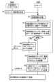
(ステップS1)
利用者が指紋センサ20に指を置いて、ICカード100を非接触な外部装置のリーダ/ライタ200にかざす。(Step S1)
A user places a finger on the
それにより、非接触な外部装置のリーダ/ライタ200の電磁界がアンテナコイル1へ誘導する電圧が指紋認証ICチップ30の通信部31に加わる。 Thereby, the voltage induced to the
(ステップS1’)
通信部31は、外部装置のリーダ/ライタ200の電磁界によってアンテナコイル1に誘導された電圧を整流して電源回路40に加えて電源回路40に電力を充電する。(Step S1')
The communication unit 31 rectifies the voltage induced in the
(ステップS2)
指紋認証ICチップ30の指紋照合手段33が、通信部31が電力を充電した電源回路40から電力を供給されて動作し、利用者の指が置かれた指紋センサ20を動作させて利用者の指紋データを受信する。(Step S2)
The fingerprint collation means 33 of the fingerprint
(ステップS3)
指紋認証ICチップ30の指紋照合手段33は、指紋センサ20により取得された利用者の指紋データを、指紋認証ICチップ30内に保持されている利用者の指紋データと照合することで、利用者の指紋データを認証する。(Step S3)
The fingerprint collation means 33 of the fingerprint
(ステップS4)
指紋照合手段33が利用者の指紋認証が行えない場合は、または、指紋センサ20によ
り取得された利用者の指紋データが、指紋認証ICチップ30内に保持された指紋データと合致しない場合は、通信部31がエラーレスポンス信号を外部装置のリーダ/ライタ200に送信する。次に、ステップS2の処理に戻る。(Step S4)
If the fingerprint verification means 33 cannot authenticate the user's fingerprint, or if the user's fingerprint data acquired by the
ここで、利用者の指が指紋センサ20に置かれていない場合は、指紋照合手段33が利用者の指紋認証が行えず、通信部31がエラーレスポンス信号を外部装置に送信し、また、主要ICモジュール10は電源回路40に接続されず、未稼働状態にある。 Here, if the user's finger is not placed on the
(ステップS5)
指紋認証ICチップ30は、指紋照合手段33が利用者の指紋認証に成功すると、電源回路40を主要ICモジュール10に接続する電源スイッチ41をONにし主要ICモジュール10を動作させる。(Step S5)
The fingerprint
(ステップS6)
主要ICモジュール10は、指紋認証ICチップ30によって電源スイッチ41がONにされて電源回路40に接続されることで起動する。(Step S6)
The
起動した主要ICモジュール10は、指紋認証ICチップ30から、外部装置のリーダ/ライタ200との通信を引継ぎ動作する。 The activated
すなわち、主要ICモジュール10のカードマネージャ13が、指紋認証ICチップ30の通信部31に仲介させて、アンテナコイル1を介して外部装置のリーダ/ライタ200と通信して外部装置からのコマンドを受信する。そして、カードマネージャ13は、外部装置から受信したコマンドを実行した結果のレスポンス電文を外部装置のリーダ/ライタ200に送信する。 That is, the card manager 13 of the
そして、主要ICモジュール10の制御手段11が、記憶手段12が記憶しているICカード100のプログラムに従って、外部装置との間で取引を開始する。 Then, the control means 11 of the
以上の様にICカード100が動作することで、指紋認証ICチップ30の指紋照合手段33が利用者の指紋認証に成功するまでの間は、主要ICモジュール10が電源回路40に接続されず未稼働状態にある。その間は、指紋認証ICチップ30の通信部31が、外部装置のリーダ/ライタ200から受信したコマンドデータに応答し、レスポンス処理を行う。 By operating the
その様に、主要ICモジュール10の動作を停止しているので、利用者の意図しない外部装置のリーダ/ライタ200が主要ICモジュール10にアクセスすることができない。それにより、悪意の第三者が不正な外部装置のリーダ/ライタ200を用いて非接触で利用者のICカード100と通信できない。 Since the operation of the
こうして、第三者の不正な非接触ICカード通信によるICカード100の主要ICモジュール10へのアクセスを防止でき、ICカード100のセキュリティを向上させる事ができる効果がある。 In this way, it is possible to prevent access to the
1・・・アンテナコイル
2・・・外部接触端子
3・・・配線
4・・・アンテナシート
5・・・カード基材
10・・・主要ICモジュール
11・・・制御手段
12・・・記憶手段
12a・・・システム記憶領域
12b・・・ファイル記憶領域
13・・・カードマネージャ
20・・・指紋センサ
30・・・指紋認証ICチップ
31・・・通信部
32・・・指紋データ記憶手段
33・・・指紋照合手段
40・・・電源回路
41・・・電源スイッチ
100・・・ICカード
200・・・外部装置のリーダ/ライタ
DF・・・専用ファイル
MF・・・主ファイル
Claims (3)
Translated fromJapanese前記指紋認証ICチップが通信部と指紋データ記憶手段と指紋照合手段を有し、
前記アンテナコイルを前記通信部に接続し、
前記通信部が、前記アンテナコイルが受け取った電力を電源回路に蓄積する手段と、前記アンテナコイルから受信した外部装置のコマンドへ返信する手段を有し、
前記指紋照合手段が利用者の指紋データを認証した場合に、前記主要ICモジュールに前記電源回路を接続して前記主要ICモジュールを動作させ、前記主要ICモジュールと外部装置の前記アンテナコイルを介した通信を前記通信部が仲介する
ことを特徴とするICカード。An IC card having an antenna coil, a main IC module, a fingerprint sensor, and a fingerprint authentication IC chip,
the fingerprint authentication IC chip has a communication unit, fingerprint data storage means, and fingerprint collation means;
connecting the antenna coil to the communication unit;
The communication unit has means for accumulating power received by the antenna coil in a power supply circuit, and means for replying to a command of an external device received from the antenna coil,
When the fingerprint collation means authenticates the user's fingerprint data, the power circuit is connected to the main IC module to operate the main IC module, and the main IC module andthe antenna coil of the external device An IC card, wherein said communication unit mediates communication.
ことを特徴とするICカード。2. An IC card according to claim 1, wherein said main IC module is a dual interface IC module having external contact terminals for direct connection and communication with terminals provided on an external device. .
ことを特徴とするICカード。
3. The IC card according to claim 1, wherein said fingerprint authentication IC chip is embedded inside a card substrate and is not exposed on the surface.
Priority Applications (1)
| Application Number | Priority Date | Filing Date | Title |
|---|---|---|---|
| JP2019048096AJP7322439B2 (en) | 2019-03-15 | 2019-03-15 | IC card |
Applications Claiming Priority (1)
| Application Number | Priority Date | Filing Date | Title |
|---|---|---|---|
| JP2019048096AJP7322439B2 (en) | 2019-03-15 | 2019-03-15 | IC card |
Publications (2)
| Publication Number | Publication Date |
|---|---|
| JP2020149534A JP2020149534A (en) | 2020-09-17 |
| JP7322439B2true JP7322439B2 (en) | 2023-08-08 |
Family
ID=72430657
Family Applications (1)
| Application Number | Title | Priority Date | Filing Date |
|---|---|---|---|
| JP2019048096AActiveJP7322439B2 (en) | 2019-03-15 | 2019-03-15 | IC card |
Country Status (1)
| Country | Link |
|---|---|
| JP (1) | JP7322439B2 (en) |
Families Citing this family (4)
| Publication number | Priority date | Publication date | Assignee | Title |
|---|---|---|---|---|
| JP7141757B2 (en)* | 2020-11-17 | 2022-09-26 | シソウル カンパニー リミテッド | fingerprint card |
| JP7439843B2 (en)* | 2022-01-28 | 2024-02-28 | 大日本印刷株式会社 | Electronic information storage medium, IC card, processing method, and program |
| KR20240096423A (en)* | 2022-12-14 | 2024-06-26 | 코나아이 (주) | smart card |
| KR20250034713A (en)* | 2023-09-04 | 2025-03-11 | 엘지이노텍 주식회사 | Smart ic substrate, smart ic module and ic card including the same |
Citations (6)
| Publication number | Priority date | Publication date | Assignee | Title |
|---|---|---|---|---|
| US20050253683A1 (en) | 2004-05-17 | 2005-11-17 | Identification Technology Group | Biometrically authenticated portable access device |
| US20060113381A1 (en) | 2004-11-29 | 2006-06-01 | John Hochstein | Batteryless contact fingerprint-enabled smartcard that enables contactless capability |
| JP2012238126A (en) | 2011-05-10 | 2012-12-06 | Secure Design Solutions Inc | Ic card with fingerprint authentication |
| JP2017531893A (en) | 2014-10-10 | 2017-10-26 | ズワイプ アクティーゼルスカブ | Non-contact biometric identification device that allows multiple configurations |
| US20180174013A1 (en) | 2015-05-26 | 2018-06-21 | Crucialtec Co., Ltd. | Smart card including fingerprint detection device and driving method thereof |
| JP2018529155A (en) | 2015-08-07 | 2018-10-04 | ズワイプ アクティーゼルスカブ | Secure passive RFID device |
- 2019
- 2019-03-15JPJP2019048096Apatent/JP7322439B2/enactiveActive
Patent Citations (6)
| Publication number | Priority date | Publication date | Assignee | Title |
|---|---|---|---|---|
| US20050253683A1 (en) | 2004-05-17 | 2005-11-17 | Identification Technology Group | Biometrically authenticated portable access device |
| US20060113381A1 (en) | 2004-11-29 | 2006-06-01 | John Hochstein | Batteryless contact fingerprint-enabled smartcard that enables contactless capability |
| JP2012238126A (en) | 2011-05-10 | 2012-12-06 | Secure Design Solutions Inc | Ic card with fingerprint authentication |
| JP2017531893A (en) | 2014-10-10 | 2017-10-26 | ズワイプ アクティーゼルスカブ | Non-contact biometric identification device that allows multiple configurations |
| US20180174013A1 (en) | 2015-05-26 | 2018-06-21 | Crucialtec Co., Ltd. | Smart card including fingerprint detection device and driving method thereof |
| JP2018529155A (en) | 2015-08-07 | 2018-10-04 | ズワイプ アクティーゼルスカブ | Secure passive RFID device |
Also Published As
| Publication number | Publication date |
|---|---|
| JP2020149534A (en) | 2020-09-17 |
Similar Documents
| Publication | Publication Date | Title |
|---|---|---|
| JP7322439B2 (en) | IC card | |
| US8811959B2 (en) | Bluetooth enabled credit card with a large data storage volume | |
| JP4653087B2 (en) | Program and secure module holder | |
| JP4682498B2 (en) | Communication device and memory management method for communication device | |
| US7992789B2 (en) | Method for making a secure personal card and its working process | |
| US7819329B2 (en) | Method of activating a fingerprint identification process of a smart card according to a given condition and a device thereof | |
| US9633300B2 (en) | Apparatus having communication means and a receiving member for a chip card | |
| US7286691B1 (en) | Devices and methods for biometric authentication | |
| US20160171201A1 (en) | External Secure Unit | |
| US20190220582A1 (en) | Biometrically authorisable device | |
| CN110062933A (en) | Fingerprint recognition card and the power supply operation method for utilizing fingerprint recognition card | |
| EP3642778A1 (en) | Incremental enrolment algorithm | |
| JP2019513256A (en) | Fingerprint authentication device | |
| US20120196531A1 (en) | Coordinating multiple contactless data carriers | |
| JP2000123144A (en) | Contactless ic card | |
| JP2004220175A (en) | Information card, information card mounting device, information card device, information card processing device, and information card processing method | |
| JP2000123143A (en) | Ic card | |
| US10515299B2 (en) | Document with sensor means | |
| WO2020181150A1 (en) | Biometric card with display | |
| GB2551955A (en) | Fingerprint authorisable device | |
| KR101729748B1 (en) | Fingerprint recognition card and authentication method using the same | |
| KR101074778B1 (en) | Sensor tag and method for authenticating for the same | |
| JP5459845B2 (en) | Portable electronic device, method for controlling portable electronic device, and IC card | |
| JP2015060407A (en) | IC card, portable terminal, and IC card processing system | |
| US12353946B2 (en) | Multipath authentication of security-relevant applications and devices |
Legal Events
| Date | Code | Title | Description |
|---|---|---|---|
| A621 | Written request for application examination | Free format text:JAPANESE INTERMEDIATE CODE: A621 Effective date:20220224 | |
| A977 | Report on retrieval | Free format text:JAPANESE INTERMEDIATE CODE: A971007 Effective date:20221214 | |
| A131 | Notification of reasons for refusal | Free format text:JAPANESE INTERMEDIATE CODE: A131 Effective date:20230117 | |
| A521 | Request for written amendment filed | Free format text:JAPANESE INTERMEDIATE CODE: A523 Effective date:20230313 | |
| RD03 | Notification of appointment of power of attorney | Free format text:JAPANESE INTERMEDIATE CODE: A7423 Effective date:20230525 | |
| TRDD | Decision of grant or rejection written | ||
| A01 | Written decision to grant a patent or to grant a registration (utility model) | Free format text:JAPANESE INTERMEDIATE CODE: A01 Effective date:20230627 | |
| A61 | First payment of annual fees (during grant procedure) | Free format text:JAPANESE INTERMEDIATE CODE: A61 Effective date:20230710 | |
| R150 | Certificate of patent or registration of utility model | Ref document number:7322439 Country of ref document:JP Free format text:JAPANESE INTERMEDIATE CODE: R150 |