JP7321026B2 - EDGE RING, PLACE, SUBSTRATE PROCESSING APPARATUS, AND SUBSTRATE PROCESSING METHOD - Google Patents
EDGE RING, PLACE, SUBSTRATE PROCESSING APPARATUS, AND SUBSTRATE PROCESSING METHODDownload PDFInfo
- Publication number
- JP7321026B2 JP7321026B2JP2019143057AJP2019143057AJP7321026B2JP 7321026 B2JP7321026 B2JP 7321026B2JP 2019143057 AJP2019143057 AJP 2019143057AJP 2019143057 AJP2019143057 AJP 2019143057AJP 7321026 B2JP7321026 B2JP 7321026B2
- Authority
- JP
- Japan
- Prior art keywords
- edge ring
- ring
- inner edge
- substrate
- height
- Prior art date
- Legal status (The legal status is an assumption and is not a legal conclusion. Google has not performed a legal analysis and makes no representation as to the accuracy of the status listed.)
- Active
Links
Images


Classifications
- H—ELECTRICITY
- H01—ELECTRIC ELEMENTS
- H01J—ELECTRIC DISCHARGE TUBES OR DISCHARGE LAMPS
- H01J37/00—Discharge tubes with provision for introducing objects or material to be exposed to the discharge, e.g. for the purpose of examination or processing thereof
- H01J37/32—Gas-filled discharge tubes
- H01J37/32431—Constructional details of the reactor
- H01J37/32623—Mechanical discharge control means
- H01J37/32642—Focus rings
- H—ELECTRICITY
- H01—ELECTRIC ELEMENTS
- H01L—SEMICONDUCTOR DEVICES NOT COVERED BY CLASS H10
- H01L21/00—Processes or apparatus adapted for the manufacture or treatment of semiconductor or solid state devices or of parts thereof
- H01L21/67—Apparatus specially adapted for handling semiconductor or electric solid state devices during manufacture or treatment thereof; Apparatus specially adapted for handling wafers during manufacture or treatment of semiconductor or electric solid state devices or components ; Apparatus not specifically provided for elsewhere
- H01L21/683—Apparatus specially adapted for handling semiconductor or electric solid state devices during manufacture or treatment thereof; Apparatus specially adapted for handling wafers during manufacture or treatment of semiconductor or electric solid state devices or components ; Apparatus not specifically provided for elsewhere for supporting or gripping
- H01L21/687—Apparatus specially adapted for handling semiconductor or electric solid state devices during manufacture or treatment thereof; Apparatus specially adapted for handling wafers during manufacture or treatment of semiconductor or electric solid state devices or components ; Apparatus not specifically provided for elsewhere for supporting or gripping using mechanical means, e.g. chucks, clamps or pinches
- H01L21/68714—Apparatus specially adapted for handling semiconductor or electric solid state devices during manufacture or treatment thereof; Apparatus specially adapted for handling wafers during manufacture or treatment of semiconductor or electric solid state devices or components ; Apparatus not specifically provided for elsewhere for supporting or gripping using mechanical means, e.g. chucks, clamps or pinches the wafers being placed on a susceptor, stage or support
- H01L21/68735—Apparatus specially adapted for handling semiconductor or electric solid state devices during manufacture or treatment thereof; Apparatus specially adapted for handling wafers during manufacture or treatment of semiconductor or electric solid state devices or components ; Apparatus not specifically provided for elsewhere for supporting or gripping using mechanical means, e.g. chucks, clamps or pinches the wafers being placed on a susceptor, stage or support characterised by edge profile or support profile
- B—PERFORMING OPERATIONS; TRANSPORTING
- B23—MACHINE TOOLS; METAL-WORKING NOT OTHERWISE PROVIDED FOR
- B23Q—DETAILS, COMPONENTS, OR ACCESSORIES FOR MACHINE TOOLS, e.g. ARRANGEMENTS FOR COPYING OR CONTROLLING; MACHINE TOOLS IN GENERAL CHARACTERISED BY THE CONSTRUCTION OF PARTICULAR DETAILS OR COMPONENTS; COMBINATIONS OR ASSOCIATIONS OF METAL-WORKING MACHINES, NOT DIRECTED TO A PARTICULAR RESULT
- B23Q3/00—Devices holding, supporting, or positioning work or tools, of a kind normally removable from the machine
- B23Q3/15—Devices for holding work using magnetic or electric force acting directly on the work
- H—ELECTRICITY
- H01—ELECTRIC ELEMENTS
- H01J—ELECTRIC DISCHARGE TUBES OR DISCHARGE LAMPS
- H01J37/00—Discharge tubes with provision for introducing objects or material to be exposed to the discharge, e.g. for the purpose of examination or processing thereof
- H01J37/32—Gas-filled discharge tubes
- H01J37/32431—Constructional details of the reactor
- H01J37/32715—Workpiece holder
- H—ELECTRICITY
- H01—ELECTRIC ELEMENTS
- H01L—SEMICONDUCTOR DEVICES NOT COVERED BY CLASS H10
- H01L21/00—Processes or apparatus adapted for the manufacture or treatment of semiconductor or solid state devices or of parts thereof
- H01L21/02—Manufacture or treatment of semiconductor devices or of parts thereof
- H01L21/04—Manufacture or treatment of semiconductor devices or of parts thereof the devices having potential barriers, e.g. a PN junction, depletion layer or carrier concentration layer
- H01L21/18—Manufacture or treatment of semiconductor devices or of parts thereof the devices having potential barriers, e.g. a PN junction, depletion layer or carrier concentration layer the devices having semiconductor bodies comprising elements of Group IV of the Periodic Table or AIIIBV compounds with or without impurities, e.g. doping materials
- H01L21/30—Treatment of semiconductor bodies using processes or apparatus not provided for in groups H01L21/20 - H01L21/26
- H01L21/302—Treatment of semiconductor bodies using processes or apparatus not provided for in groups H01L21/20 - H01L21/26 to change their surface-physical characteristics or shape, e.g. etching, polishing, cutting
- H01L21/306—Chemical or electrical treatment, e.g. electrolytic etching
- H01L21/3065—Plasma etching; Reactive-ion etching
- H—ELECTRICITY
- H01—ELECTRIC ELEMENTS
- H01L—SEMICONDUCTOR DEVICES NOT COVERED BY CLASS H10
- H01L21/00—Processes or apparatus adapted for the manufacture or treatment of semiconductor or solid state devices or of parts thereof
- H01L21/67—Apparatus specially adapted for handling semiconductor or electric solid state devices during manufacture or treatment thereof; Apparatus specially adapted for handling wafers during manufacture or treatment of semiconductor or electric solid state devices or components ; Apparatus not specifically provided for elsewhere
- H01L21/67005—Apparatus not specifically provided for elsewhere
- H01L21/67011—Apparatus for manufacture or treatment
- H01L21/67017—Apparatus for fluid treatment
- H01L21/67063—Apparatus for fluid treatment for etching
- H01L21/67069—Apparatus for fluid treatment for etching for drying etching
- H—ELECTRICITY
- H01—ELECTRIC ELEMENTS
- H01L—SEMICONDUCTOR DEVICES NOT COVERED BY CLASS H10
- H01L21/00—Processes or apparatus adapted for the manufacture or treatment of semiconductor or solid state devices or of parts thereof
- H01L21/67—Apparatus specially adapted for handling semiconductor or electric solid state devices during manufacture or treatment thereof; Apparatus specially adapted for handling wafers during manufacture or treatment of semiconductor or electric solid state devices or components ; Apparatus not specifically provided for elsewhere
- H01L21/683—Apparatus specially adapted for handling semiconductor or electric solid state devices during manufacture or treatment thereof; Apparatus specially adapted for handling wafers during manufacture or treatment of semiconductor or electric solid state devices or components ; Apparatus not specifically provided for elsewhere for supporting or gripping
- H01L21/6831—Apparatus specially adapted for handling semiconductor or electric solid state devices during manufacture or treatment thereof; Apparatus specially adapted for handling wafers during manufacture or treatment of semiconductor or electric solid state devices or components ; Apparatus not specifically provided for elsewhere for supporting or gripping using electrostatic chucks
- H01L21/6833—Details of electrostatic chucks
- H—ELECTRICITY
- H01—ELECTRIC ELEMENTS
- H01L—SEMICONDUCTOR DEVICES NOT COVERED BY CLASS H10
- H01L21/00—Processes or apparatus adapted for the manufacture or treatment of semiconductor or solid state devices or of parts thereof
- H01L21/67—Apparatus specially adapted for handling semiconductor or electric solid state devices during manufacture or treatment thereof; Apparatus specially adapted for handling wafers during manufacture or treatment of semiconductor or electric solid state devices or components ; Apparatus not specifically provided for elsewhere
- H01L21/683—Apparatus specially adapted for handling semiconductor or electric solid state devices during manufacture or treatment thereof; Apparatus specially adapted for handling wafers during manufacture or treatment of semiconductor or electric solid state devices or components ; Apparatus not specifically provided for elsewhere for supporting or gripping
- H01L21/687—Apparatus specially adapted for handling semiconductor or electric solid state devices during manufacture or treatment thereof; Apparatus specially adapted for handling wafers during manufacture or treatment of semiconductor or electric solid state devices or components ; Apparatus not specifically provided for elsewhere for supporting or gripping using mechanical means, e.g. chucks, clamps or pinches
- H01L21/68714—Apparatus specially adapted for handling semiconductor or electric solid state devices during manufacture or treatment thereof; Apparatus specially adapted for handling wafers during manufacture or treatment of semiconductor or electric solid state devices or components ; Apparatus not specifically provided for elsewhere for supporting or gripping using mechanical means, e.g. chucks, clamps or pinches the wafers being placed on a susceptor, stage or support
- H01L21/68742—Apparatus specially adapted for handling semiconductor or electric solid state devices during manufacture or treatment thereof; Apparatus specially adapted for handling wafers during manufacture or treatment of semiconductor or electric solid state devices or components ; Apparatus not specifically provided for elsewhere for supporting or gripping using mechanical means, e.g. chucks, clamps or pinches the wafers being placed on a susceptor, stage or support characterised by a lifting arrangement, e.g. lift pins
- H—ELECTRICITY
- H01—ELECTRIC ELEMENTS
- H01L—SEMICONDUCTOR DEVICES NOT COVERED BY CLASS H10
- H01L21/00—Processes or apparatus adapted for the manufacture or treatment of semiconductor or solid state devices or of parts thereof
- H01L21/67—Apparatus specially adapted for handling semiconductor or electric solid state devices during manufacture or treatment thereof; Apparatus specially adapted for handling wafers during manufacture or treatment of semiconductor or electric solid state devices or components ; Apparatus not specifically provided for elsewhere
- H01L21/683—Apparatus specially adapted for handling semiconductor or electric solid state devices during manufacture or treatment thereof; Apparatus specially adapted for handling wafers during manufacture or treatment of semiconductor or electric solid state devices or components ; Apparatus not specifically provided for elsewhere for supporting or gripping
- H01L21/687—Apparatus specially adapted for handling semiconductor or electric solid state devices during manufacture or treatment thereof; Apparatus specially adapted for handling wafers during manufacture or treatment of semiconductor or electric solid state devices or components ; Apparatus not specifically provided for elsewhere for supporting or gripping using mechanical means, e.g. chucks, clamps or pinches
- H01L21/68714—Apparatus specially adapted for handling semiconductor or electric solid state devices during manufacture or treatment thereof; Apparatus specially adapted for handling wafers during manufacture or treatment of semiconductor or electric solid state devices or components ; Apparatus not specifically provided for elsewhere for supporting or gripping using mechanical means, e.g. chucks, clamps or pinches the wafers being placed on a susceptor, stage or support
- H01L21/68757—Apparatus specially adapted for handling semiconductor or electric solid state devices during manufacture or treatment thereof; Apparatus specially adapted for handling wafers during manufacture or treatment of semiconductor or electric solid state devices or components ; Apparatus not specifically provided for elsewhere for supporting or gripping using mechanical means, e.g. chucks, clamps or pinches the wafers being placed on a susceptor, stage or support characterised by a coating or a hardness or a material
- H—ELECTRICITY
- H02—GENERATION; CONVERSION OR DISTRIBUTION OF ELECTRIC POWER
- H02N—ELECTRIC MACHINES NOT OTHERWISE PROVIDED FOR
- H02N13/00—Clutches or holding devices using electrostatic attraction, e.g. using Johnson-Rahbek effect
- H—ELECTRICITY
- H01—ELECTRIC ELEMENTS
- H01J—ELECTRIC DISCHARGE TUBES OR DISCHARGE LAMPS
- H01J2237/00—Discharge tubes exposing object to beam, e.g. for analysis treatment, etching, imaging
- H01J2237/32—Processing objects by plasma generation
- H01J2237/33—Processing objects by plasma generation characterised by the type of processing
- H01J2237/334—Etching
- H—ELECTRICITY
- H01—ELECTRIC ELEMENTS
- H01J—ELECTRIC DISCHARGE TUBES OR DISCHARGE LAMPS
- H01J37/00—Discharge tubes with provision for introducing objects or material to be exposed to the discharge, e.g. for the purpose of examination or processing thereof
- H01J37/32—Gas-filled discharge tubes
- H01J37/32009—Arrangements for generation of plasma specially adapted for examination or treatment of objects, e.g. plasma sources
- H01J37/32082—Radio frequency generated discharge
Landscapes
- Engineering & Computer Science (AREA)
- Physics & Mathematics (AREA)
- Microelectronics & Electronic Packaging (AREA)
- General Physics & Mathematics (AREA)
- Manufacturing & Machinery (AREA)
- Computer Hardware Design (AREA)
- Condensed Matter Physics & Semiconductors (AREA)
- Power Engineering (AREA)
- Plasma & Fusion (AREA)
- Chemical & Material Sciences (AREA)
- Analytical Chemistry (AREA)
- Mechanical Engineering (AREA)
- Drying Of Semiconductors (AREA)
- Plasma Technology (AREA)
Description
Translated fromJapanese本開示は、エッジリング、載置台、基板処理装置及び基板処理方法に関する。 The present disclosure relates to an edge ring, a mounting table, a substrate processing apparatus, and a substrate processing method.
基板の周囲に配置されるエッジリング(フォーカスリングともいう。)の一部を上下に駆動する技術が提案されている。例えば、特許文献1は、フォーカスリングを内側フォーカスリングと外側フォーカスリングとに分割し、内側フォーカスリング又は外側フォーカスリングをプッシャーピンにより持ち上げることを提案する。これにより、持ち上げたフォーカスリングに付着した堆積物のプラズマによる分解除去を促進する。 A technique has been proposed for vertically driving a part of an edge ring (also called a focus ring) arranged around a substrate. For example, Patent Document 1 proposes dividing the focus ring into an inner focus ring and an outer focus ring, and lifting the inner focus ring or the outer focus ring by a pusher pin. This promotes plasma decomposition and removal of deposits adhering to the lifted focus ring.
エッジリングは、プラズマに曝露されることで消耗する。エッジリングが消耗すると、基板とエッジリングの上部に形成されるシースに段差が生じ、基板のエッジ領域においてイオンが斜めに入射することで、基板のエッジ領域におけるエッチング形状の垂直性が失われ、基板のエッジ領域のプロセス特性が変化する。そこで、例えば、特許文献2は、エッジリングの消耗に応じてエッジリングの一部を上下に駆動し、シースの段差をなくすことを提案する。 Edge rings are consumed by exposure to plasma. When the edge ring is worn out, a step occurs between the substrate and the sheath formed on the edge ring, and ions are obliquely incident on the edge region of the substrate. The process characteristics of the edge region of the substrate change. Therefore, for example, Patent Document 2 proposes to eliminate the step of the sheath by driving a part of the edge ring up and down according to wear of the edge ring.
本開示は、複数の部材から構成されるエッジリングにおいて、一の部材を他の部材に対して上下動させた場合のプロセス特性の変動を抑制可能なエッジリング、載置台、基板処理装置及び基板処理方法を提供する。 The present disclosure provides an edge ring, a mounting table, a substrate processing apparatus, and a substrate that can suppress variations in process characteristics when one member is moved up and down relative to another member in an edge ring configured from a plurality of members. Provide processing methods.
本開示の一の態様によれば、第1のエッジリングと、前記第1のエッジリングの側面に近接する側面を有し、前記第1のエッジリングの側面に沿って上下方向に移動可能な第2のエッジリングとを備え、前記第1のエッジリングの側面と前記第2のエッジリングの側面とは、前記第2のエッジリングの移動範囲において少なくとも一部が対向する、エッジリングが提供される。 According to one aspect of the present disclosure, the device has a first edge ring and a side surface adjacent to the side surface of the first edge ring, and is vertically movable along the side surface of the first edge ring. a second edge ring, wherein a side surface of the first edge ring and a side surface of the second edge ring are at least partially opposed in a range of movement of the second edge ring. be done.
一の側面によれば、複数の部材から構成されるエッジリングにおいて、一の部材を他の部材に対して上下動させた場合のプロセス特性の変動を抑制することができる。 According to one aspect, in the edge ring composed of a plurality of members, fluctuations in process characteristics can be suppressed when one member is vertically moved with respect to the other members.
以下、図面を参照して本開示を実施するための形態について説明する。各図面において、同一構成部分には同一符号を付し、重複した説明を省略する場合がある。 Hereinafter, embodiments for carrying out the present disclosure will be described with reference to the drawings. In each drawing, the same components are denoted by the same reference numerals, and redundant description may be omitted.
[基板処理装置]
一実施形態に係る基板処理装置1について、図1を用いて説明する。図1は、一実施形態に係る基板処理装置1の一例を示す断面模式図である。[Substrate processing equipment]
A substrate processing apparatus 1 according to one embodiment will be described with reference to FIG. FIG. 1 is a schematic cross-sectional view showing an example of a substrate processing apparatus 1 according to one embodiment.
基板処理装置1は、チャンバ10を備える。チャンバ10は、その中に内部空間10sを提供する。チャンバ10はチャンバ本体12を含む。チャンバ本体12は、略円筒形状を有する。チャンバ本体12は、例えばアルミニウムから形成される。チャンバ本体12の内壁面上には、耐腐食性を有する膜が設けられている。当該膜は、酸化アルミニウム、酸化イットリウムなどのセラミックであってよい。 A substrate processing apparatus 1 includes a
チャンバ本体12の側壁には、通路12pが形成されている。基板Wは、通路12pを通して内部空間10sとチャンバ10の外部との間で搬送される。通路12pは、チャンバ本体12の側壁に沿って設けられるゲートバルブ12gにより開閉される。 A
チャンバ本体12の底部上には、支持部13が設けられている。支持部13は、絶縁材料から形成される。支持部13は、略円筒形状を有する。支持部13は、内部空間10sの中で、チャンバ本体12の底部から上方に延在している。支持部13は、上部に支持台14を有する。支持台14は、内部空間10sの中において、基板Wを支持するように構成されている。 A
支持台14は、下部電極18及び静電チャック20を有する。支持台14は、電極プレート16を更に有し得る。電極プレート16は、アルミニウムなどの導体から形成され、略円盤形状を有する。下部電極18は、電極プレート16上に設けられている。下部電極18は、アルミニウムなどの導体から形成されて、略円盤形状を有する。下部電極18は、電極プレート16に電気的に接続されている。 The support table 14 has a
静電チャック20は、下部電極18上に設けられている。静電チャック20の上面に基板Wが載置される。静電チャック20は、本体及び電極を有する。静電チャック20の本体は、略円盤形状を有し、誘電体から形成される。静電チャック20の電極は、膜状の電極であり、静電チャック20の本体内に設けられている。静電チャック20の電極は、スイッチ20sを介して直流電源20pに接続されている。静電チャック20の電極に直流電源20pからの電圧が印加されると、静電チャック20と基板Wとの間に静電引力が発生する。その静電引力により、基板Wが静電チャック20に保持される。 An
下部電極18の周縁部上には、基板Wのエッジを囲むように、エッジリング25が配置される。エッジリング25は、基板Wに対するプラズマ処理の面内均一性を向上させる。エッジリング25は、内側エッジリング25aと外側エッジリング25bとに分割されている。内側エッジリング25aは概ね外側エッジリング25bの内側に配置されている。外側エッジリング25bの上面は、載置面に置かれている状態の内側エッジリング25aの上面よりも高い。 An
下部電極18の内部には、流路18fが設けられている。流路18fには、チャンバ10の外部に設けられているチラーユニット(図示しない)から配管22aを介して熱交換媒体(例えば冷媒)が供給される。流路18fに供給された熱交換媒体は、配管22bを介してチラーユニットに戻される。基板処理装置1では、静電チャック20上に載置された基板Wの温度が、熱交換媒体と下部電極18との熱交換により、調整される。 Inside the
基板処理装置1には、ガス供給ライン24が設けられている。ガス供給ライン24は、伝熱ガス供給機構からの伝熱ガス(例えばHeガス)を、静電チャック20の上面と基板Wの裏面との間に供給する。 A gas supply line 24 is provided in the substrate processing apparatus 1 . The gas supply line 24 supplies heat transfer gas (for example, He gas) from a heat transfer gas supply mechanism between the upper surface of the
基板処理装置1は、上部電極30を更に備える。上部電極30は、支持台14の上方に設けられている。上部電極30は、部材32を介して、チャンバ本体12の上部に支持されている。部材32は、絶縁性を有する材料から形成される。上部電極30と部材32は、チャンバ本体12の上部開口を閉じている。 The substrate processing apparatus 1 further includes an
上部電極30は、天板34及び支持体36を含み得る。天板34の下面は、内部空間10sの側の下面であり、内部空間10sを画成する。天板34は、発生するジュール熱の少ない低抵抗の導電体又は半導体から形成され得る。天板34は、天板34をその板厚方向に貫通する複数のガス吐出孔34aを有する。
支持体36は、天板34を着脱自在に支持する。支持体36は、アルミニウムなどの導電性材料から形成される。支持体36の内部には、ガス拡散室36aが設けられている。支持体36は、ガス拡散室36aから下方に延びる複数のガス孔36bを有する。複数のガス孔36bは、複数のガス吐出孔34aにそれぞれ連通している。支持体36には、ガス導入口36cが形成されている。ガス導入口36cは、ガス拡散室36aに接続している。ガス導入口36cには、ガス供給管38が接続されている。 The
ガス供給管38には、バルブ群41、流量制御器群42、及びガスソース群40が接続されている。ガスソース群40、バルブ群41、及び流量制御器群42、は、ガス供給部を構成している。ガスソース群40は、複数のガスソースを含む。バルブ群41は、複数の開閉バルブを含む。流量制御器群42は、複数の流量制御器を含む。流量制御器群42の複数の流量制御器の各々は、マスフローコントローラ又は圧力制御式の流量制御器である。ガスソース群40の複数のガスソースの各々は、バルブ群41の対応の開閉バルブ、及び流量制御器群42の対応の流量制御器を介して、ガス供給管38に接続されている。 A group of
基板処理装置1では、チャンバ本体12の内壁面及び支持部13の外周に沿って、シールド46が着脱自在に設けられている。シールド46は、チャンバ本体12に反応副生物が付着することを防止する。シールド46は、例えば、アルミニウムから形成された母材の表面に耐腐食性を有する膜を形成することにより構成される。耐腐食性を有する膜は、酸化イットリウムなどのセラミックから形成され得る。 In the substrate processing apparatus 1 , a
支持部13とチャンバ本体12の側壁との間には、バッフルプレート48が設けられている。バッフルプレート48は、例えば、アルミニウムから形成された母材の表面に耐腐食性を有する膜(酸化イットリウムなどの膜)を形成することにより構成される。バッフルプレート48には、複数の貫通孔が形成されている。バッフルプレート48の下方、且つ、チャンバ本体12の底部には、排気口12eが設けられている。排気口12eには、排気管52を介して排気装置50が接続されている。排気装置50は、圧力調整弁及びターボ分子ポンプなどの真空ポンプを含む。 A
基板処理装置1は、第1の高周波(Radio Frequency)電源62及び第2の高周波電源64を備えている。第1の高周波電源62は、第1の高周波電力を発生する電源である。第1の高周波電力は、プラズマの生成に適した周波数を有する。第1の高周波電力の周波数は、例えば27MHz~100MHzの範囲内の周波数である。第1の高周波電源62は、整合器66を介して上部電極30に接続されている。整合器66は、第1の高周波電源62の出力インピーダンスと負荷側(上部電極30側)のインピーダンスを整合させるための回路を有する。なお、第1の高周波電源62は、整合器66を介して、下部電極18に接続されていてもよい。第1の高周波電源62は、一例のプラズマ生成部を構成している。 The substrate processing apparatus 1 includes a first radio frequency (Radio Frequency)
第2の高周波電源64は、第2の高周波電力を発生する電源である。第2の高周波電力は、第1の高周波電力の周波数よりも低い周波数を有する。第1の高周波電力と共に第2の高周波電力が用いられる場合には、第2の高周波電力は基板Wにイオンを引き込むためのバイアス用の高周波電力として用いられる。第2の高周波電力の周波数は、例えば400kHz~13.56MHzの範囲内の周波数である。第2の高周波電源64は、整合器68及び電極プレート16を介して下部電極18に接続されている。整合器68は、第2の高周波電源64の出力インピーダンスと負荷側(下部電極18側)のインピーダンスを整合させるための回路を有する。 The second high
なお、第1の高周波電力を用いずに、第2の高周波電力を用いて、即ち、単一の高周波電力のみを用いてプラズマを生成してもよい。この場合、第2の高周波電力の周波数は、13.56MHzよりも大きな周波数、例えば40MHzであってもよい。また、この場合には、基板処理装置1は、第1の高周波電源62及び整合器66を備えなくてもよい。第2の高周波電源64は一例のプラズマ生成部を構成する。 Plasma may be generated using the second high-frequency power instead of the first high-frequency power, that is, using only a single high-frequency power. In this case, the frequency of the second high frequency power may be a frequency greater than 13.56 MHz, such as 40 MHz. Also, in this case, the substrate processing apparatus 1 does not need to include the first high-
基板処理装置1においてガスが、ガス供給部から内部空間10sに供給されて、プラズマを生成する。また、第1の高周波電力及び/又は第2の高周波電力が供給されることにより、上部電極30と下部電極18との間で高周波電界が生成される。生成された高周波電界がプラズマを生成する。 In the substrate processing apparatus 1, gas is supplied from the gas supply unit to the
基板処理装置1は、制御部80を更に備え得る。制御部80は、プロセッサ、メモリなどの記憶部、入力装置、表示装置、信号の入出力インターフェイス等を備えるコンピュータであり得る。制御部80は、基板処理装置1の各部を制御する。制御部80では、入力装置を用いて、オペレータが基板処理装置1を管理するためにコマンドの入力操作等を行うことができる。また、制御部80では、表示装置により、基板処理装置1の稼働状況を可視化して表示することができる。さらに、記憶部には、制御プログラム及びレシピデータが格納されている。制御プログラムは、基板処理装置1で各種処理を実行するために、プロセッサによって実行される。プロセッサが、制御プログラムを実行し、レシピデータに従って基板処理装置1の各部を制御する。 The substrate processing apparatus 1 may further include a
[エッジリング]
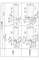
次に、エッジリングの構造及びエッチレートについて、図2及び図3を参照しながら説明する。図2(a)は、比較例に係るエッジリング125の上下駆動とRFパス(高周波の経路)を示す図である。図2(b)は、一実施形態に係るエッジリング25の上下駆動とRFパスを示す図である。図3(a)は、比較例に係る内側エッジリング125aの高さとエッチングレートとの相関情報を示す図である。図3(b)は、一実施形態に係る内側エッジリング25aの高さとエッチングレートとの相関情報を示す図である。[Edge ring]
Next, the structure and etch rate of the edge ring will be described with reference to FIGS. 2 and 3. FIG. FIG. 2A is a diagram showing vertical driving of the
図2(a)に示す比較例に係るエッジリング125は、内側エッジリング125aと外側エッジリング125bとを有する。内側エッジリング125a及び外側エッジリング125bとは環状の部材である。内側エッジリング125aは、外側エッジリング125bに近接して配置されている。外側エッジリング125bは、下部電極18の載置面に固定されている。外側エッジリング125bは、内周側に凹部を有し、凹部の底部は、内側エッジリング125aが載置される載置面125b2となっている。内側エッジリング125aは、外側エッジリング125bの内周側に凹部の載置面125b2に載置される。この状態で、内側エッジリング125aの側面125a1と外側エッジリング125bの側面125b1とが対向する。 The
外側エッジリング125bの凹部の下部には、貫通孔が形成されている。貫通孔にリフトピン27を挿通させ、リフトピン27を上下に駆動することで、内側エッジリング125aが外側エッジリング125bの載置面125b2から離れ、上下方向に駆動する。 A through hole is formed in the lower portion of the recess of the
図2(b)に示す一実施形態に係るエッジリング25は、内側エッジリング25aと外側エッジリング25bとを有する。内側エッジリング25a及び外側エッジリング25bとは環状の部材である。内側エッジリング25a及び外側エッジリング25bの材質は、抵抗値が高い石英、アルミナ等の誘電体以外であればよい。内側エッジリング25a及び外側エッジリング25bの材質は、例えば、シリコン、炭化シリコン等の半導体又は導体から形成され得る。内側エッジリング25a及び外側エッジリング25bは同一の材質で形成されてもよく、異なる材質で形成されてもよい。 The
内側エッジリング25aは、外側エッジリング25bの側面に近接する側面を有する。外側エッジリング25bは、下部電極18の載置面に固定されている。外側エッジリング25bは、固定された第1のエッジリングの一例である。 The
外側エッジリング25bは、側面25b1の内周側に内側エッジリング25aを載置する載置部25b4を有する。一実施形態に係るエッジリング25では、載置部25b4は凹部を形成している。載置部25b4の上面25b2、すなわち凹部の底部には、内側エッジリング25aが載置される。外側エッジリング25bの側面25b1と、内側エッジリング25aの側面25a1は、内側エッジリング25aの上下方向の移動範囲において、少なくとも一部が対向する。内側エッジリング25aは、最下位置において載置部25b4の上面25b2に配置される。この状態で、内側エッジリング25aの側面25a1と外側エッジリング25bの側面25b1とは、全面が対向する。 The
外側エッジリング25bの凹部の下部には、貫通孔が形成されている。貫通孔にリフトピン27を挿通させ、リフトピン27に接続された駆動部26がリフトピン27を上下に駆動する(図1参照)。これにより、内側エッジリング25aは、リフトピン27により押上げられ又は下げられ、上下方向に駆動する。内側エッジリング25aは、第1のエッジリングの側面に近接する側面を有し、前記第1のエッジリングの側面に沿って上下方向に移動可能な第2のエッジリングの一例である。 A through hole is formed in the lower portion of the recess of the
図2(a)及び(b)は、内側エッジリング125a及び内側エッジリング25aを上下方向に移動させる前及び移動させた後の状態をそれぞれ図示している。図2(a)の左図は、内側エッジリング125aが載置面125b2に載置されている状態を示し、図2(b)の左図は、内側エッジリング25aが載置面25b2に載置されている状態を示す。 FIGS. 2(a) and 2(b) respectively show the state before and after the
図2(b)の外側エッジリング25bの底面から載置面25b2までの厚さQ2は、図2(a)の外側エッジリング125bの底面から載置面125b2までの厚さQ1と同一である。つまり、Q2=Q1である。図2(b)の外側エッジリング25bの底面から上面25b3までの厚さH2は、図2(a)の外側エッジリング125bの底面から上面125b3までの厚さH1よりも厚い。つまり、H2>H1である。厚さH1、H2以外の外側エッジリング125bと外側エッジリング25bの形状は同一である。また、内側エッジリング125aと内側エッジリング25aの形状は同一である。 The thickness Q2 from the bottom surface of the
図2(a)に示す比較例において載置面125b2に載置されている内側エッジリング125aの上面125a3と外側エッジリング125bの上面125b3とは同じ高さである。H2>H1により、図2(b)に示す本実施形態において載置面25b2に載置されている内側エッジリング25aの上面25a3は、外側エッジリング25bの上面25b3よりも低くなる。 In the comparative example shown in FIG. 2A, the upper surface 125a3 of the
図2(a)の右図は、内側エッジリング125aを載置面125b2から高さPまで上昇させたときの状態を示し、図2(b)の右図は、内側エッジリング25aを載置面25b2から図2(a)と同じ高さPまで上昇させたときの状態を示す。 The right diagram of FIG. 2(a) shows the state when the
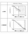
例えばエッチングレートの面内均一性を確保する等、プロセス特性を制御するためには、基板のエッジ領域の制御が重要である。そこで、以下、比較例の内側エッジリング125a及び本実施形態の内側エッジリング25aの駆動量に対する基板のエッジ領域の制御について考察する。なお、エッジ領域は、基板の端から数mm~10mm程度の領域をいう。 Controlling the edge region of the substrate is important for controlling process characteristics, such as ensuring in-plane uniformity of the etching rate. Therefore, the control of the edge region of the substrate with respect to the driving amount of the
基板(300mmのウエハ)のエッジ領域の148mmの位置におけるエッチングレートを、内側エッジリング125a及び内側エッジリング25aを上下方向に移動させて測定した。その測定結果の一例が、図3(a)及び(b)のグラフである。 The etching rate at a position of 148 mm in the edge region of the substrate (wafer of 300 mm) was measured by vertically moving the
図3(a)は、比較例に係る内側エッジリング125aが載置面125b2に載置されている状態をP0として、横軸に内側エッジリング125aの高さPを示し、縦軸に高さPを変化させたときの基板のエッジ領域におけるエッチングレートを示す。 In FIG. 3A, the horizontal axis indicates the height P of the
図3(b)は、本実施形態に係る内側エッジリング25aが上面25b2に載置されている状態をP0として、横軸に内側エッジリング25aの高さPを示し、縦軸に高さPを変化させたときの基板のエッジ領域におけるエッチングレートを示す。図3(a)及び(b)の縦軸のエッチングレートは、下に行くほど小さくなり(low)、上に行くほど大きくなる(high)。 In FIG. 3B, the horizontal axis indicates the height P of the
これによれば、比較例に係るエッジリング125では、内側エッジリング125aの高さが、P0~P1の間は、内側エッジリング125aの上昇に応じてエッチングレートが一定の傾きで変化した。エッジリング125の高さがP1以上になると、内側エッジリング125aの上昇に応じたエッチングレートの傾きが変わった。このように内側エッジリング125aが上下方向に駆動する範囲においてエッチングレートの傾きが変わる特異点があると、特異点の前と比較して内側エッジリング125aの制御量とエッチングレートとの相関関係が変化する部分(図3(a)の斜線部)が生じる。そうすると、内側エッジリング125aの上下方向の移動範囲において、内側エッジリング125aの高さに応じた基板のエッジ領域のプロセス特性の制御が複雑になる。 According to this, in the
そして、比較例における特異点は、図2(a)の右図に示すように、内側エッジリング125aの下面が外側エッジリング125bの上面125b3に到達した位置に対応する。換言すれば、比較例における特異点は、内側エッジリング125aの側面125a1が外側エッジリング125bの側面125b1と対向しなくなった位置に対応する。 The singular point in the comparative example corresponds to the position where the lower surface of the
内側エッジリング125aを載置面125a2から上昇させるとき、ある高さまでは、内側エッジリング125aの側面125a1と外側エッジリング125bの側面125b1との少なくとも一部が対向する。この場合、内側エッジリング125aの側面125a1と外側エッジリング125bの側面125b1との間には電位差はほぼ生じない。しかしながら、図3(a)の例では、図2に示す内側エッジリング125aの高さPがP1~P2の間になると、内側エッジリング125aの側面125a1と外側エッジリング125bの側面125b1との対向面は存在しない状態となる。そうすると、高さPがP1のときを特異点として、この特異点を境界に内側エッジリング125aの側面125a1と外側エッジリング125bの側面125b1との間の電位差が大きくなる。これにより、外側エッジリング125bの側面125b1と内側エッジリング125aの側面125a1との間のRFパスを確保できなくなる。 When the
直流電圧の場合、内側エッジリング125aと外側エッジリング125bとの間に隙間があると抵抗値が高くなり、その隙間に電流は通らない。しかしながら、比較例及び本実施形態では、エッジリング125及びエッジリング25には、第2の高周波電源64から下部電極18に印加された高周波電流が流れる。この場合、内側エッジリング125aの側面125a1と外側エッジリング125bの側面125b1とが近接対向していれば、真空空間の隙間がコンデンサの機能を有する。よって、隙間D(図2(b)参照)の両側に位置する内側エッジリング125aと外側エッジリング125bとはほぼ同電位になる。 In the case of a DC voltage, if there is a gap between the
よって、内側エッジリング125aの側面125a1と外側エッジリング125bの側面125b1とは、内側エッジリング125aの移動範囲において少なくとも一部が対向していれば、RFパスが確保されることがわかった。 Therefore, it has been found that the RF path is ensured if at least a portion of the side surface 125a1 of the
一方、内側エッジリング125aの側面125a1と外側エッジリング125bの側面125b1とが対向しなくなると、内側エッジリング125aの側面125a1と外側エッジリング125bの側面125b1との間の電位差が大きくなる。 On the other hand, when the side surface 125a1 of the
この結果、内側エッジリング125aの側面125a1と外側エッジリング125bの側面125b1との対向面がない状態に変化したときを特異点として、内側エッジリング125aの移動量に対する基板のエッジ領域のプロセス特性の相関関係が変化する。これにより、基板のエッジ領域の調整幅が、エッジリング125の高さの制御に対して特異点の前後で変わり、内側エッジリング125aの移動量に対する基板のエッジ領域の制御が複雑になるために、基板のエッジ領域の制御の精度が低下する。 As a result, the process characteristic of the edge region of the substrate with respect to the amount of movement of the
これに対して、本実施形態に係るエッジリング25は、内側エッジリング25aが上下方向に移動する範囲内において内側エッジリング25aの側面25a1と外側エッジリング25bの側面25b1とは、少なくとも一部が対向するようにエッジリング25を構成する。つまり、内側エッジリング25aの上面25a3よりも外側エッジリング25bの上面125b3を上方向に延長し、外側エッジリング25bの上面25b3の高さを、上面25b2に載置されている内側エッジリング25aの上面25a3の高さよりも高くする。 On the other hand, in the
これにより、内側エッジリング25aが駆動範囲の最上位置に制御された場合にも、内側エッジリング25aの側面25a1と外側エッジリング25bの側面25b1とは、少なくとも一部が対向する。この結果、図2(b)に示すように、内側エッジリング25aが最上位置を含むいずれの高さに制御されたとしても、内側エッジリング25aの側面25a1と外側エッジリング25bの側面25b1との間においてRFパスが確保される。よって、内側エッジリング25aが最上位置を含むいずれの高さに制御されたとしても、内側エッジリング25aと外側エッジリング25bとは、電気的に接続可能である。 As a result, even when the
これにより、図3(b)に示すように、内側エッジリング25aの高さPが基板の中心P0から基板のエッジのP1'(基板の端から数mm~10mm)まで、エッチングレートを直線的に変化させることができる。これにより、内側エッジリング25aの制御量とエッチングレートとが上下方向の移動範囲において一律に比例するため、基板のエッジ領域のプロセス特性の制御性を容易かつ精度良く行うことができる。 As a result, as shown in FIG. 3B, the height P of the
なお、図2(b)に示す内側エッジリング125aの側面125a1と外側エッジリング125bの側面125b1との間の隙間Dは、当該エッチング装置で使用される周波数の高周波の経路を確保可能な距離であればよい。 Note that the gap D between the side surface 125a1 of the
上記実施形態では、内側エッジリング25aと外側エッジリング25bとの近接面は、両部材の側面25a1及び25b1である例を挙げて説明したが、これに限られない。以下、内側エッジリング25aと外側エッジリング25bとの近接面が側面25a1及び25b1以外を含む変形例について、図4を参照しながら説明する。 In the above-described embodiment, the adjacent surfaces of the
[変形例]
図4は、一実施形態の変形例に係るエッジリング25の一例を示す図である。図4(a)の変形例1に係るエッジリング25は、内側エッジリング25aと外側エッジリング25bとに2分割される。内側エッジリング25aは外側エッジリング25bの内側に配置され、外側エッジリング25bの上面25b3は内側エッジリング25aの上面25a3よりも高い。上記実施形態との違いは、外側エッジリング25bに内側エッジリング25aを載置する凹部がなく、内側エッジリング25aを載置する上面25b2がフラットに形成されている点である。変形例1に係るエッジリング25では、内側エッジリング25aの上下方向の移動範囲において内側エッジリング25aの側面25a1と外側エッジリング25bの側面25b1との少なくとも一部が対向する構成になっている。[Modification]
FIG. 4 is a diagram showing an example of the
図4(b)の変形例2に係るエッジリング25は、内側エッジリング25aと外側エッジリング25bとに2分割される。内側エッジリング25aは外側エッジリング25bの内側に配置され、外側エッジリング25bの上面25b3は内側エッジリング25aの上面25a3よりも高い。上記実施形態との違いは、外側エッジリング25bに内側エッジリング25aを載置する載置面がなく、内側エッジリング25aは下部電極18に載置される点である。変形例2に係るエッジリング25では、内側エッジリング25aの上下方向の移動範囲において内側エッジリング25aの側面25a1と外側エッジリング25bの側面25b1との少なくとも一部が対向する構成になっている。 The
なお、変形例1及び変形例2では、外側エッジリング25bは、第1のエッジリングの一例である。内側エッジリング25aは、第1のエッジリングの側面に近接する側面を有し、第1のエッジリングの側面に沿って上下方向に移動可能な第2のエッジリングの一例である。 It should be noted that in Modifications 1 and 2, the
図4(c)の変形例3に係るエッジリング25は、内側エッジリング25aと外側エッジリング25bとに2分割される。内側エッジリング25aは外側エッジリング25bの内側に配置され、内側エッジリング25aの上面25a3は外側エッジリング25bの上面25b3よりも高い。変形例2との違いは、内側エッジリング25aが固定され、外側エッジリング25bが上下に駆動可能である点である。このように、RFパスが確保できれば駆動側のエッジリングが固定側のエッジリングの外側にあってもよい。変形例3に係るエッジリング25では、外側エッジリング25bの上下方向の駆動範囲において外側エッジリング25bの側面25b5と内側エッジリング25aの側面25a4との少なくとも一部が対向する構成になっている。 The
なお、変形例3では、外側エッジリング25bは、上下方向に移動可能な第2のエッジリングの一例であり、内側エッジリング25aは、第2のエッジリングに近接して固定される第1のエッジリングの一例である。 In Modification 3, the
図4(d)の変形例4に係るエッジリング25は、内側エッジリング25aと外側エッジリング25bと最内エッジリング25cとに3分割される。内側エッジリング25aは外側エッジリング25bの内側に配置され、外側エッジリング25bの上面25b3は内側エッジリング25aの上面25a3よりも高い。上記実施形態との違いは、外側エッジリング25bが、内側エッジリング25aに近接する側面25b1において最内エッジリング25cと分割されている点である。変形例4の構造では、内側エッジリング25aは最内エッジリング25cに形成された載置面25c2に載置されている。変形例4に係るエッジリング25では、内側エッジリング25aの上下方向の駆動範囲において内側エッジリング25aの側面25a1と外側エッジリング25bの側面25b1との少なくとも一部が対向する構成になっている。 The
図4(e)の変形例5に係るエッジリング25は、内側エッジリング25aと外側エッジリング25bと最内エッジリング25cとに3分割される。内側エッジリング25aは外側エッジリング25bの内側に配置され、外側エッジリング25bの上面25b3は内側エッジリング25aの上面25a3よりも高い。変形例4との違いは、最内エッジリング25cは内側エッジリング25aの内周面よりも内側に配置され、内側エッジリング25aは下部電極18の載置面に載置される点である。なお、変形例5では、外側エッジリング25bの上面25b3が内側エッジリング25aの上面25a3よりも高くなっているが、最内エッジリング25cの上面25c3が内側エッジリング25aの上面25a3よりも高くなっていてもよい。外側エッジリング25bの上面25b3と最内エッジリング25cの上面25c3の両面が、内側エッジリング25aの上面25a3よりも高くなっていてもよい。 The
なお、変形例4及び変形例5では、内側エッジリング25aは、上下方向に移動可能な第2のエッジリングの一例である。また、外側エッジリング25b及び最内エッジリング25cは、第2のエッジリングに近接して固定される第1のエッジリングの一例である。変形例4及び変形例5は、第1のエッジリングが複数の部材から構成される場合の一例である。 In addition, in Modifications 4 and 5, the
このように、第1のエッジリングは、複数に分割されてもよい。第1のエッジリングが複数に分割されている場合、第2のエッジリングと、複数の第1のエッジリングの少なくともいずれかと、の側面の少なくとも一部が第2のエッジリングの上下方向の移動範囲において対向していればよい。 Thus, the first edge ring may be divided into multiple pieces. When the first edge ring is divided into a plurality of parts, at least a part of the side surface of the second edge ring and at least one of the plurality of first edge rings moves the second edge ring in the vertical direction. It suffices if they face each other in the range.
図4(f)の変形例6に係るエッジリング25は、内側エッジリング25aと外側エッジリング25bとに2分割される。内側エッジリング25aは外側エッジリング25bの内側に配置され、外側エッジリング25bの外周側の面25b6と側面25b1との交点が内側エッジリング25aの上面25a3よりも高い。上記実施形態との違いは、外側エッジリング25bの外周側の面25b6が上面25b2に垂直ではなく、ラウンドしている点である。 The
なお、変形例6では、内側エッジリング25aは、上下方向に駆動可能な第2のエッジリングの一例であり、外側エッジリング25bは、第2のエッジリングに近接して固定される第1のエッジリングの一例である。変形例6に係るエッジリング25では、内側エッジリング25aの上下方向の移動範囲において内側エッジリング25aの側面25a1と外側エッジリング25bの側面25b1との少なくとも一部が対向する構成になっている。 In Modification 6, the
駆動側の第2のエッジリングが基板側にある場合、第2のエッジリングを基板の近傍で上下に移動させることができる。これにより、基板のエッジ領域の制御性を高めることができる。ただし、固定側の第1のエッジリングが基板側にある場合にも、上記に説明したように第2のエッジリングの上下方向の移動範囲において第1のエッジリングの側面と第2のエッジリングの側面との少なくとも一部が対向する構成にする。これにより、基板のエッジ領域の制御性を高め、基板のエッジ領域においても良好なプロセス特性を得ることができる。 If the drive side second edge ring is on the substrate side, the second edge ring can be moved up and down in the vicinity of the substrate. This can improve the controllability of the edge region of the substrate. However, even when the fixed-side first edge ring is located on the substrate side, the side surface of the first edge ring and the second edge ring are separated from each other in the vertical movement range of the second edge ring as described above. At least a part of the side of the is opposed. As a result, the controllability of the edge region of the substrate can be improved, and good process characteristics can be obtained even in the edge region of the substrate.
また、エッジリングを第1のエッジリングと第2のエッジリングとに分割することで、例えば消耗した側のエッジリングだけを交換するなど、エッジリングの一部のみを交換することができ、コストを低減することができる。特に、分割されたエッジリングのうち、基板に近い側のエッジリングの消耗は、基板のエッジ領域のプロセス特性に与える影響が大きいため、基板に近い側のエッジリングだけを変えることができるというメリットがある。 In addition, by dividing the edge ring into the first edge ring and the second edge ring, only a part of the edge ring can be replaced, for example, only the edge ring on the worn side can be replaced, reducing the cost. can be reduced. Especially, among the divided edge rings, wear of the edge ring closer to the substrate greatly affects the process characteristics of the edge region of the substrate, so there is an advantage that only the edge ring closer to the substrate can be changed. There is
[エッジリングの移動方法を含む基板処理方法]
次に、一実施形態のエッジリング25の移動方法を含む基板処理方法について、図5を参照しながら説明する。図5は、一実施形態に係るエッジリングの移動方法を含む基板処理方法の一例を示すフローチャートである。本処理は、制御部80により制御される。[Substrate Processing Method Including Edge Ring Moving Method]
Next, a substrate processing method including a method of moving the
なお、本処理を開始するタイミングは、エッジリング25の消耗量、特に基板の周囲に配置された内側エッジリング25aの消耗量に応じて設定してもよい。本処理を開始するタイミングは、第1の高周波電源62及び/又は第2の高周波電源64からの高周波電力の印加時間に応じて設定してもよい。本処理を開始するタイミングは、基板のエッジ領域のプロセス特性(例えば、エッチングレート)の測定結果に応じて設定してもよい。また、本処理を開始するタイミングは、1枚の基板が処理される毎、複数枚の基板が処理される毎、ロット毎又は複数ロットが処理される毎に設定してもよい。 The timing for starting this process may be set according to the amount of wear of the
本処理が開始されると、制御部80は、予め測定された内側エッジリング25aの高さと基板のエッジ領域(例えば148mm)におけるエッチングレートとの相関情報を取得する(ステップS1)。この相関情報は、エッチングレートの値に応じて制御すべき内側エッジリング25aの高さを示す。エッチングレートに応じた内側エッジリング25aの高さに内側エッジリング25aを上下方向に移動することで、基板のエッジ領域におけるプロセス特性を精度良く制御できる。プロセス特性の一例としては、エッチングレートの他、エッチング形状、CD(Critical Dimension)値が挙げられる。 When this process is started, the
次に、制御部80は、取得した相関情報に基づき、所望のエッチングレートに対する内側エッジリング25aの目標の高さまでの移動量を決定する(ステップS2)。次に、制御部80は、内側エッジリング25aの上下方向の移動を開始する(ステップS3)。 Next, based on the obtained correlation information, the
次に、制御部80は、内側エッジリング25aが目標の高さに到達したか否かを判定する(ステップS4)。制御部80は、内側エッジリング25aが目標の高さに到達していないと判定した場合、内側エッジリング25aの移動量が、内側エッジリング25aの上下方向の移動範囲を超えたか否かを判定する(ステップS5)。内側エッジリング25aの上下方向の移動範囲を超えたか否かは、内側エッジリング25aの移動範囲の上限値に基づき判定される。内側エッジリング25aの移動範囲の上限値は、内側エッジリング25aの側面と外側エッジリング25bの側面の少なくとも一部が対向する条件を満たす値に予め設定されている。制御部80は、内側エッジリング25aの移動量が、内側エッジリング25aの上下方向の移動範囲を超えていないと判定した場合、ステップS4に戻る。そして、制御部80は、内側エッジリング25aが目標の高さに到達したか、又は、内側エッジリング25aの移動量が内側エッジリング25aの上下方向の移動範囲を超えたと判定されるまで、ステップS4及びステップS5の処理を繰り返し実行する。 Next, the
制御部80は、内側エッジリング25aが目標の高さになったと判定したか又は内側エッジリング25aの移動量がその上下方向の移動範囲を超えたと判定した場合、内側エッジリング25aの上下方向の移動を停止し(ステップS6)、本処理を終了する。 When the
以上、本実施形態及び変形例のエッジリング、載置台、基板処理装置及び基板処理方法によれば、内側エッジリング25a及び外側エッジリング25bに分割したエッジリング25において、分割された一方のエッジリングを上下方向に移動させる。エッジリング25の上下方向の移動範囲において、内側エッジリング25aの側面25a1と外側エッジリング25bの側面25b1との少なくとも一部が対向しているため、RFパスは確保される。よって、内側エッジリング25aと外側エッジリング25bとは電気的に接続される。これにより、移動側のエッジリングを、上下方向の移動範囲において移動させることで、基板のエッジ領域の制御を安定して行うことができる。 As described above, according to the edge ring, the mounting table, the substrate processing apparatus, and the substrate processing method of the present embodiment and modifications, in the
以上に説明したように、本実施形態及び変形例は、複数の部材から構成され、一の部材を他の部材に対して上下方向に移動させた場合のプロセス特性の変動を抑制可能なエッジリング25を提供できる。また、分割したエッジリング25の上下方向の移動に対して、分割された一方の部材から他方の部材に伝わる交流電圧の抵抗を変化し難くすることができる。 As described above, according to the present embodiment and the modified example, the edge ring is composed of a plurality of members and is capable of suppressing variations in process characteristics when one member is vertically moved with respect to another member. 25 can be provided. In addition, it is possible to make it difficult for the resistance of the AC voltage transmitted from one of the divided members to the other to change with respect to the vertical movement of the divided
今回開示された一実施形態に係るエッジリング、載置台、基板処理装置及び基板処理方法は、すべての点において例示であって制限的なものではないと考えられるべきである。上記の実施形態は、添付の請求の範囲及びその主旨を逸脱することなく、様々な形態で変形及び改良が可能である。上記複数の実施形態に記載された事項は、矛盾しない範囲で他の構成も取り得ることができ、また、矛盾しない範囲で組み合わせることができる。 The edge ring, the mounting table, the substrate processing apparatus, and the substrate processing method according to the embodiment disclosed this time should be considered as examples and not restrictive in all respects. The embodiments described above can be modified and improved in various ways without departing from the scope and spirit of the appended claims. The items described in the above multiple embodiments can take other configurations within a consistent range, and can be combined within a consistent range.
本開示の基板処理装置は、Atomic Layer Deposition(ALD)装置、Capacitively Coupled Plasma(CCP)、Inductively Coupled Plasma(ICP)、Radial Line Slot Antenna(RLSA)、Electron Cyclotron Resonance Plasma(ECR)、Helicon Wave Plasma(HWP)のいずれのタイプのプラズマ処理装置においても適用可能である。 The substrate processing apparatus of the present disclosure includes an Atomic Layer Deposition (ALD) apparatus, Capacitively Coupled Plasma (CCP), Inductively Coupled Plasma (ICP), Radial Line Slot Antenna (RLSA), Electron Cyclotron Resonance Plasma (ECR), Helicon Wave Plasma ( HWP) can be applied to any type of plasma processing apparatus.
また、基板処理装置の一例としてプラズマ処理装置を挙げて説明したが、基板処理装置は、基板に所定の処理(例えば、成膜処理、エッチング処理等)を施す装置であればよく、プラズマ処理装置に限定されるものではない。 Further, although the plasma processing apparatus has been described as an example of the substrate processing apparatus, the substrate processing apparatus may be any apparatus that performs predetermined processing (eg, film formation processing, etching processing, etc.) on the substrate. is not limited to
1 基板処理装置
10 チャンバ
14 支持台
16 電極プレート
18 下部電極
20 静電チャック
25 エッジリング
25a 内側エッジリング
25b 外側エッジリング
25b4 載置部
62 第1の高周波電源
64 第2の高周波電源
80 制御部1
Claims (15)
Translated fromJapanese前記第1のエッジリングの側面に近接する側面を有し、前記第1のエッジリングの側面に沿って上下方向に移動可能な第2のエッジリングと、を備えるエッジリングであり、
前記第1のエッジリングの側面と前記第2のエッジリングの側面とは、前記第2のエッジリングの移動範囲において少なくとも一部が対向し、
前記エッジリングがプラズマに暴露されることで消耗する前の状態において、前記第1のエッジリングの側面の高さは、前記第2のエッジリングの側面の高さよりも高い、エッジリング。a first edge ring;
a second edge ring having a side surface adjacent to the side surface of the first edge ring and vertically movable along the side surface of the first edgering ;
a side surface of the first edge ring and a side surface of the second edge ringare at least partially opposed in a range of movement of the second edge ring;
The edge ring, wherein the height of the sides of the first edge ring is higher than the height of the sides of the second edge ring before the edge ring is consumed by exposure to plasma.
請求項1に記載のエッジリング。the first edge ring and the second edge ring are electrically connectable;
The edge ring of Claim1 .
請求項1又は2に記載のエッジリング。wherein the second edge ring is arranged radially inner than the first edge ring;
The edge ring according to claim 1or 2 .
前記第2のエッジリングは、最下位置において前記載置部の上面に配置される、
請求項3に記載のエッジリング。The first edge ring has a mounting portion for mounting the second edge ring on the inner peripheral side of the side surface at least partially facing the side surface of the second edge ring,
The second edge ring is arranged on the upper surface of the mounting part at the lowest position,
The edge ring of claim3 .
請求項1~4のいずれか一項に記載のエッジリング。The first edge ring is composed of a plurality of members,
The edge ring according to any one of claims1-4 .
請求項1~5のいずれか一項に記載のエッジリング。The first edge ring and the second edge ring are made of the same material,
The edge ring according to any one of claims1-5 .
請求項1~6のいずれか一項に記載のエッジリング。The material of the first edge ring and the second edge ring is Si or SiC,
The edge ring according to any one of claims1-6 .
前記基板が載置される領域を囲むように前記載置面の上に配置される請求項1~7のいずれか一項に記載のエッジリングと、
前記エッジリングが備える第2のエッジリングを上下方向に移動させるための移動手段と、
を備える、載置台。a mounting surface on which the substrate is mounted;
an edge ring according to any one of claims 1 to7 , arranged on the mounting surface so as to surround a region on which the substrate is mounted;
moving means for vertically moving a second edge ring included in the edge ring;
A mounting table.
前記チャンバ内に配置される請求項8に記載の載置台と、
を備える、基板処理装置。a chamber for processing the substrate;
a mounting table according to claim8 arranged in the chamber;
A substrate processing apparatus comprising:
前記基板が載置される領域を囲むように載置台上に配置される第1のエッジリングと、
前記第1のエッジリングの側面に近接する側面を有し、前記第1のエッジリングの側面に沿って上下方向に移動可能な第2のエッジリングと、を備えるエッジリングと、を有する基板処理装置において実行される基板処理方法であって、
前記エッジリングは、前記第1のエッジリングの側面と前記第2のエッジリングの側面とは、前記第2のエッジリングの移動範囲において少なくとも一部が対向し、
前記エッジリングがプラズマに暴露されることで消耗する前の状態において、前記第1のエッジリングの側面の高さは、前記第2のエッジリングの側面の高さよりも高く、
前記基板処理方法は、
エッジリングの高さと基板のエッジのプロセス特性との相関情報を取得する工程と、
前記相関情報に基づき、前記第2のエッジリングの高さを決定する工程と、
前記第1のエッジリングの側面と前記第2のエッジリングの側面とは、前記第2のエッジリングの移動範囲において少なくとも一部が対向する範囲で、決定した前記第2のエッジリングの高さまで前記第2のエッジリングを上下方向に移動させる工程と、
を有する、基板処理方法。a chamber for processing a substrate;
a first edge ring arranged on the mounting table so as to surround an area on which the substrate is mounted;
a second edge ring having a side surface adjacent to a side surface of the first edge ring and vertically movable along the side surface of the first edge ring. A substrate processing method performed in an apparatus, comprising:
The edge ring has a side surface of the first edge ring and a side surface of the second edge ring that are at least partially opposed in a range of movement of the second edge ring,
In a state before the edge ring is consumed by exposure to plasma, the height of the side surface of the first edge ring is higher than the height of the side surface of the second edge ring;
The substrate processing method includes
obtaining correlation information between the height of the edge ring and the process characteristics of the edge of the substrate;
determining the height of the second edge ring based on the correlation information;
The side surface of the first edge ring and the side surface of the second edge ring are at least partially opposed in the range of movement of the second edge ring, and the determined height of the second edge ring is reached. vertically moving the second edge ring;
A substrate processing method comprising:
前記第1のエッジリングは、前記第2のエッジリングの内周側に配置される第1の部分と、前記第2のエッジリングの外周側に配置され、第1の側面を有する第2の部分と、を含み、 The first edge ring has a first portion arranged on the inner peripheral side of the second edge ring and a second portion arranged on the outer peripheral side of the second edge ring and having a first side surface. including the part and
前記第2のエッジリングは、前記第1の側面に近接する第2の側面を有し、前記第1の側面に沿って垂直方向に移動可能に構成され、 the second edge ring has a second side adjacent to the first side and is configured to be vertically movable along the first side;
前記第1の側面と前記第2の側面とは、前記第2のエッジリングの移動範囲において少なくとも一部が対向可能に構成され、 The first side surface and the second side surface are configured such that at least a portion of the first side surface and the second side surface can face each other within a movement range of the second edge ring,
前記第1の部分と前記第2の部分とは、同一の材料で構成される、エッジリング。 The edge ring, wherein the first portion and the second portion are made of the same material.
前記第2のエッジリングは、前記第3の部分の上方で、垂直方向に移動可能に構成される、請求項11に記載のエッジリング。 12. The edge ring of claim 11, wherein the second edge ring is configured to be vertically movable over the third portion.
Priority Applications (5)
| Application Number | Priority Date | Filing Date | Title |
|---|---|---|---|
| JP2019143057AJP7321026B2 (en) | 2019-08-02 | 2019-08-02 | EDGE RING, PLACE, SUBSTRATE PROCESSING APPARATUS, AND SUBSTRATE PROCESSING METHOD |
| TW109124392ATWI889693B (en) | 2019-08-02 | 2020-07-20 | Edge ring, substrate support, substrate processing apparatus and method |
| KR1020200091743AKR20210015664A (en) | 2019-08-02 | 2020-07-23 | Edge ring, substrate support, substrate processing apparatus and method |
| CN202010731343.0ACN112309819B (en) | 2019-08-02 | 2020-07-27 | Edge ring, mounting table, substrate processing device and substrate processing method |
| US16/941,976US11984301B2 (en) | 2019-08-02 | 2020-07-29 | Edge ring, substrate support, substrate processing apparatus and method |
Applications Claiming Priority (1)
| Application Number | Priority Date | Filing Date | Title |
|---|---|---|---|
| JP2019143057AJP7321026B2 (en) | 2019-08-02 | 2019-08-02 | EDGE RING, PLACE, SUBSTRATE PROCESSING APPARATUS, AND SUBSTRATE PROCESSING METHOD |
Publications (2)
| Publication Number | Publication Date |
|---|---|
| JP2021027123A JP2021027123A (en) | 2021-02-22 |
| JP7321026B2true JP7321026B2 (en) | 2023-08-04 |
Family
ID=74258636
Family Applications (1)
| Application Number | Title | Priority Date | Filing Date |
|---|---|---|---|
| JP2019143057AActiveJP7321026B2 (en) | 2019-08-02 | 2019-08-02 | EDGE RING, PLACE, SUBSTRATE PROCESSING APPARATUS, AND SUBSTRATE PROCESSING METHOD |
Country Status (5)
| Country | Link |
|---|---|
| US (1) | US11984301B2 (en) |
| JP (1) | JP7321026B2 (en) |
| KR (1) | KR20210015664A (en) |
| CN (1) | CN112309819B (en) |
| TW (1) | TWI889693B (en) |
Families Citing this family (7)
| Publication number | Priority date | Publication date | Assignee | Title |
|---|---|---|---|---|
| WO2021025934A1 (en)* | 2019-08-05 | 2021-02-11 | Lam Research Corporation | Edge ring systems for substrate processing systems |
| CN112397366B (en)* | 2020-11-05 | 2023-07-14 | 北京北方华创微电子装备有限公司 | Bearing device and semiconductor reaction chamber |
| JP7492928B2 (en)* | 2021-02-10 | 2024-05-30 | 東京エレクトロン株式会社 | SUBSTRATE SUPPORT, PLASMA PROCESSING SYSTEM AND PLASMA ETCHING METHOD - Patent application |
| KR20220144766A (en)* | 2021-04-20 | 2022-10-27 | 에이에스엠 아이피 홀딩 비.브이. | Substrate processing apparatus |
| CN113308681B (en)* | 2021-05-21 | 2022-01-11 | 北京北方华创微电子装备有限公司 | Carrier device in semiconductor process equipment and semiconductor process equipment |
| WO2022271513A1 (en)* | 2021-06-24 | 2022-12-29 | Lam Research Corporation | In-line machine vision system for part tracking of substrate processing system |
| TWI886821B (en)* | 2023-03-29 | 2025-06-11 | 大陸商中微半導體設備(上海)股份有限公司 | Focusing ring, plasma processing device and operation method thereof |
Citations (3)
| Publication number | Priority date | Publication date | Assignee | Title |
|---|---|---|---|---|
| JP2012146743A (en) | 2011-01-07 | 2012-08-02 | Tokyo Electron Ltd | Substrate processing apparatus |
| US20180358211A1 (en) | 2017-06-09 | 2018-12-13 | Semes Co., Ltd. | Substrate treating apparatus |
| JP2019071369A (en) | 2017-10-11 | 2019-05-09 | 東京エレクトロン株式会社 | Plasma processing apparatus, elevation control method for focus ring, and elevation control program for focus ring |
Family Cites Families (20)
| Publication number | Priority date | Publication date | Assignee | Title |
|---|---|---|---|---|
| US6709547B1 (en)* | 1999-06-30 | 2004-03-23 | Lam Research Corporation | Moveable barrier for multiple etch processes |
| KR20080075734A (en)* | 2007-02-13 | 2008-08-19 | 삼성전자주식회사 | Process chamber |
| JP5317424B2 (en)* | 2007-03-28 | 2013-10-16 | 東京エレクトロン株式会社 | Plasma processing equipment |
| US20090151870A1 (en)* | 2007-12-14 | 2009-06-18 | Tokyo Electron Limited | Silicon carbide focus ring for plasma etching system |
| JP5741124B2 (en)* | 2011-03-29 | 2015-07-01 | 東京エレクトロン株式会社 | Plasma processing equipment |
| WO2012133585A1 (en)* | 2011-03-29 | 2012-10-04 | 東京エレクトロン株式会社 | Plasma etching device, and plasma etching method |
| US10153192B2 (en)* | 2015-09-25 | 2018-12-11 | Sumitomo Osaka Cement Co., Ltd. | Electrostatic chuck device |
| KR102709229B1 (en)* | 2015-12-07 | 2024-09-23 | 어플라이드 머티어리얼스, 인코포레이티드 | Merge Cover Ring |
| CN108369922B (en)* | 2016-01-26 | 2023-03-21 | 应用材料公司 | Wafer edge ring lifting solution |
| JP6986937B2 (en)* | 2017-01-05 | 2021-12-22 | 東京エレクトロン株式会社 | Plasma processing equipment |
| US20180190501A1 (en)* | 2017-01-05 | 2018-07-05 | Tokyo Electron Limited | Plasma processing apparatus |
| US11404249B2 (en)* | 2017-03-22 | 2022-08-02 | Tokyo Electron Limited | Substrate processing apparatus |
| JP7055039B2 (en) | 2017-03-22 | 2022-04-15 | 東京エレクトロン株式会社 | Board processing equipment |
| JP7033926B2 (en)* | 2017-04-26 | 2022-03-11 | 東京エレクトロン株式会社 | Plasma processing equipment |
| US11043400B2 (en)* | 2017-12-21 | 2021-06-22 | Applied Materials, Inc. | Movable and removable process kit |
| US10600623B2 (en)* | 2018-05-28 | 2020-03-24 | Applied Materials, Inc. | Process kit with adjustable tuning ring for edge uniformity control |
| KR20210111872A (en)* | 2018-08-13 | 2021-09-13 | 램 리써치 코포레이션 | Replaceable and/or collapsible edge ring assemblies for plasma sheath tuning incorporating edge ring positioning and centering features |
| US20200234928A1 (en)* | 2019-01-17 | 2020-07-23 | Applied Materials, Inc. | Semiconductor plasma processing equipment with wafer edge plasma sheath tuning ability |
| US11018046B2 (en)* | 2019-04-12 | 2021-05-25 | Samsung Electronics Co., Ltd. | Substrate processing apparatus including edge ring |
| TWM593655U (en)* | 2019-05-10 | 2020-04-11 | 美商蘭姆研究公司 | Semiconductor process module mid ring |
- 2019
- 2019-08-02JPJP2019143057Apatent/JP7321026B2/enactiveActive
- 2020
- 2020-07-20TWTW109124392Apatent/TWI889693B/enactive
- 2020-07-23KRKR1020200091743Apatent/KR20210015664A/enactivePending
- 2020-07-27CNCN202010731343.0Apatent/CN112309819B/enactiveActive
- 2020-07-29USUS16/941,976patent/US11984301B2/enactiveActive
Patent Citations (3)
| Publication number | Priority date | Publication date | Assignee | Title |
|---|---|---|---|---|
| JP2012146743A (en) | 2011-01-07 | 2012-08-02 | Tokyo Electron Ltd | Substrate processing apparatus |
| US20180358211A1 (en) | 2017-06-09 | 2018-12-13 | Semes Co., Ltd. | Substrate treating apparatus |
| JP2019071369A (en) | 2017-10-11 | 2019-05-09 | 東京エレクトロン株式会社 | Plasma processing apparatus, elevation control method for focus ring, and elevation control program for focus ring |
Also Published As
| Publication number | Publication date |
|---|---|
| US11984301B2 (en) | 2024-05-14 |
| CN112309819A (en) | 2021-02-02 |
| JP2021027123A (en) | 2021-02-22 |
| TW202114029A (en) | 2021-04-01 |
| US20210035783A1 (en) | 2021-02-04 |
| TWI889693B (en) | 2025-07-11 |
| KR20210015664A (en) | 2021-02-10 |
| CN112309819B (en) | 2024-11-19 |
Similar Documents
| Publication | Publication Date | Title |
|---|---|---|
| JP7321026B2 (en) | EDGE RING, PLACE, SUBSTRATE PROCESSING APPARATUS, AND SUBSTRATE PROCESSING METHOD | |
| TWI861122B (en) | Stage and plasma processing apparatus | |
| JP6556046B2 (en) | Plasma processing method and plasma processing apparatus | |
| JP7296829B2 (en) | Plasma processing apparatus, processing method, upper electrode structure | |
| JP2018098239A (en) | Mounting table and plasma processing apparatus | |
| US11978614B2 (en) | Substrate processing apparatus | |
| JP7365815B2 (en) | Mounting table and substrate processing equipment | |
| CN112420471B (en) | Edge ring, plasma processing device and method for manufacturing edge ring | |
| US11538669B2 (en) | Plasma processing apparatus | |
| KR102827625B1 (en) | Etching method and plasma processing apparatus | |
| CN112242290B (en) | Plasma processing method and plasma processing apparatus | |
| CN112530799A (en) | Method for etching silicon oxide film and plasma processing apparatus | |
| US11664198B2 (en) | Plasma processing apparatus | |
| KR20190079565A (en) | Etching method | |
| US20210142990A1 (en) | Plasma processing apparatus | |
| TW202522659A (en) | Placing table and substrate processing apparatus | |
| JP2009152233A (en) | Semiconductor manufacturing equipment | |
| JP2021125637A (en) | Plasma processing equipment and plasma processing method | |
| US20210305023A1 (en) | Edge ring and plasma processing apparatus |
Legal Events
| Date | Code | Title | Description |
|---|---|---|---|
| A621 | Written request for application examination | Free format text:JAPANESE INTERMEDIATE CODE: A621 Effective date:20220520 | |
| A131 | Notification of reasons for refusal | Free format text:JAPANESE INTERMEDIATE CODE: A131 Effective date:20230228 | |
| A977 | Report on retrieval | Free format text:JAPANESE INTERMEDIATE CODE: A971007 Effective date:20230228 | |
| A521 | Request for written amendment filed | Free format text:JAPANESE INTERMEDIATE CODE: A523 Effective date:20230426 | |
| TRDD | Decision of grant or rejection written | ||
| A01 | Written decision to grant a patent or to grant a registration (utility model) | Free format text:JAPANESE INTERMEDIATE CODE: A01 Effective date:20230627 | |
| A61 | First payment of annual fees (during grant procedure) | Free format text:JAPANESE INTERMEDIATE CODE: A61 Effective date:20230725 | |
| R150 | Certificate of patent or registration of utility model | Ref document number:7321026 Country of ref document:JP Free format text:JAPANESE INTERMEDIATE CODE: R150 |