JP7320563B2 - High temperature substrate pedestal module and its components - Google Patents
High temperature substrate pedestal module and its componentsDownload PDFInfo
- Publication number
- JP7320563B2 JP7320563B2JP2021104513AJP2021104513AJP7320563B2JP 7320563 B2JP7320563 B2JP 7320563B2JP 2021104513 AJP2021104513 AJP 2021104513AJP 2021104513 AJP2021104513 AJP 2021104513AJP 7320563 B2JP7320563 B2JP 7320563B2
- Authority
- JP
- Japan
- Prior art keywords
- stem
- adapter
- gas
- substrate pedestal
- sidewall
- Prior art date
- Legal status (The legal status is an assumption and is not a legal conclusion. Google has not performed a legal analysis and makes no representation as to the accuracy of the status listed.)
- Active
Links
- 239000000758substrateSubstances0.000titleclaimsdescription199
- NJPPVKZQTLUDBO-UHFFFAOYSA-NnovaluronChemical compoundC1=C(Cl)C(OC(F)(F)C(OC(F)(F)F)F)=CC=C1NC(=O)NC(=O)C1=C(F)C=CC=C1FNJPPVKZQTLUDBO-UHFFFAOYSA-N0.000titleclaimsdescription88
- 238000012545processingMethods0.000claimsdescription128
- 238000004891communicationMethods0.000claimsdescription53
- 239000012530fluidSubstances0.000claimsdescription50
- 230000002093peripheral effectEffects0.000claimsdescription15
- 238000012546transferMethods0.000claimsdescription11
- 239000007788liquidSubstances0.000claims2
- 239000007789gasSubstances0.000description215
- 239000004065semiconductorSubstances0.000description98
- 238000000034methodMethods0.000description49
- 238000000151depositionMethods0.000description9
- 229910010293ceramic materialInorganic materials0.000description8
- 230000008021depositionEffects0.000description8
- 238000000231atomic layer depositionMethods0.000description7
- 238000000623plasma-assisted chemical vapour depositionMethods0.000description7
- 238000010926purgeMethods0.000description7
- 238000005229chemical vapour depositionMethods0.000description5
- 229910000838Al alloyInorganic materials0.000description4
- 229910052782aluminiumInorganic materials0.000description4
- XAGFODPZIPBFFR-UHFFFAOYSA-NaluminiumChemical compound[Al]XAGFODPZIPBFFR-UHFFFAOYSA-N0.000description4
- 230000006870functionEffects0.000description4
- 239000000919ceramicSubstances0.000description3
- 238000005137deposition processMethods0.000description3
- 239000011261inert gasSubstances0.000description3
- 239000000463materialSubstances0.000description3
- 230000005404monopoleEffects0.000description3
- 239000002243precursorSubstances0.000description3
- 238000005234chemical depositionMethods0.000description2
- 238000004590computer programMethods0.000description2
- 238000009792diffusion processMethods0.000description2
- 239000010408filmSubstances0.000description2
- 238000005240physical vapour depositionMethods0.000description2
- 238000009832plasma treatmentMethods0.000description2
- 238000011112process operationMethods0.000description2
- 238000003860storageMethods0.000description2
- 230000003213activating effectEffects0.000description1
- 238000005219brazingMethods0.000description1
- 238000011109contaminationMethods0.000description1
- PMHQVHHXPFUNSP-UHFFFAOYSA-Mcopper(1+);methylsulfanylmethane;bromideChemical compoundBr[Cu].CSCPMHQVHHXPFUNSP-UHFFFAOYSA-M0.000description1
- 230000003247decreasing effectEffects0.000description1
- 238000010586diagramMethods0.000description1
- 230000000694effectsEffects0.000description1
- 238000005530etchingMethods0.000description1
- 230000007246mechanismEffects0.000description1
- 229910052751metalInorganic materials0.000description1
- 239000002184metalSubstances0.000description1
- 239000007769metal materialSubstances0.000description1
- 239000000203mixtureSubstances0.000description1
- 238000012986modificationMethods0.000description1
- 230000004048modificationEffects0.000description1
- 238000012544monitoring processMethods0.000description1
- 238000011160researchMethods0.000description1
- 238000013515scriptMethods0.000description1
- 238000004904shorteningMethods0.000description1
- 239000010409thin filmSubstances0.000description1
- 238000003466weldingMethods0.000description1
Images


Classifications
- C—CHEMISTRY; METALLURGY
- C23—COATING METALLIC MATERIAL; COATING MATERIAL WITH METALLIC MATERIAL; CHEMICAL SURFACE TREATMENT; DIFFUSION TREATMENT OF METALLIC MATERIAL; COATING BY VACUUM EVAPORATION, BY SPUTTERING, BY ION IMPLANTATION OR BY CHEMICAL VAPOUR DEPOSITION, IN GENERAL; INHIBITING CORROSION OF METALLIC MATERIAL OR INCRUSTATION IN GENERAL
- C23C—COATING METALLIC MATERIAL; COATING MATERIAL WITH METALLIC MATERIAL; SURFACE TREATMENT OF METALLIC MATERIAL BY DIFFUSION INTO THE SURFACE, BY CHEMICAL CONVERSION OR SUBSTITUTION; COATING BY VACUUM EVAPORATION, BY SPUTTERING, BY ION IMPLANTATION OR BY CHEMICAL VAPOUR DEPOSITION, IN GENERAL
- C23C16/00—Chemical coating by decomposition of gaseous compounds, without leaving reaction products of surface material in the coating, i.e. chemical vapour deposition [CVD] processes
- C23C16/44—Chemical coating by decomposition of gaseous compounds, without leaving reaction products of surface material in the coating, i.e. chemical vapour deposition [CVD] processes characterised by the method of coating
- C23C16/458—Chemical coating by decomposition of gaseous compounds, without leaving reaction products of surface material in the coating, i.e. chemical vapour deposition [CVD] processes characterised by the method of coating characterised by the method used for supporting substrates in the reaction chamber
- C23C16/4582—Rigid and flat substrates, e.g. plates or discs
- C23C16/4583—Rigid and flat substrates, e.g. plates or discs the substrate being supported substantially horizontally
- H—ELECTRICITY
- H01—ELECTRIC ELEMENTS
- H01L—SEMICONDUCTOR DEVICES NOT COVERED BY CLASS H10
- H01L21/00—Processes or apparatus adapted for the manufacture or treatment of semiconductor or solid state devices or of parts thereof
- H01L21/02—Manufacture or treatment of semiconductor devices or of parts thereof
- H01L21/02104—Forming layers
- H01L21/02107—Forming insulating materials on a substrate
- H01L21/02225—Forming insulating materials on a substrate characterised by the process for the formation of the insulating layer
- H01L21/0226—Forming insulating materials on a substrate characterised by the process for the formation of the insulating layer formation by a deposition process
- H01L21/02263—Forming insulating materials on a substrate characterised by the process for the formation of the insulating layer formation by a deposition process deposition from the gas or vapour phase
- H01L21/02271—Forming insulating materials on a substrate characterised by the process for the formation of the insulating layer formation by a deposition process deposition from the gas or vapour phase deposition by decomposition or reaction of gaseous or vapour phase compounds, i.e. chemical vapour deposition
- H01L21/02274—Forming insulating materials on a substrate characterised by the process for the formation of the insulating layer formation by a deposition process deposition from the gas or vapour phase deposition by decomposition or reaction of gaseous or vapour phase compounds, i.e. chemical vapour deposition in the presence of a plasma [PECVD]
- H—ELECTRICITY
- H01—ELECTRIC ELEMENTS
- H01L—SEMICONDUCTOR DEVICES NOT COVERED BY CLASS H10
- H01L21/00—Processes or apparatus adapted for the manufacture or treatment of semiconductor or solid state devices or of parts thereof
- H01L21/67—Apparatus specially adapted for handling semiconductor or electric solid state devices during manufacture or treatment thereof; Apparatus specially adapted for handling wafers during manufacture or treatment of semiconductor or electric solid state devices or components ; Apparatus not specifically provided for elsewhere
- H01L21/683—Apparatus specially adapted for handling semiconductor or electric solid state devices during manufacture or treatment thereof; Apparatus specially adapted for handling wafers during manufacture or treatment of semiconductor or electric solid state devices or components ; Apparatus not specifically provided for elsewhere for supporting or gripping
- H01L21/687—Apparatus specially adapted for handling semiconductor or electric solid state devices during manufacture or treatment thereof; Apparatus specially adapted for handling wafers during manufacture or treatment of semiconductor or electric solid state devices or components ; Apparatus not specifically provided for elsewhere for supporting or gripping using mechanical means, e.g. chucks, clamps or pinches
- H01L21/68714—Apparatus specially adapted for handling semiconductor or electric solid state devices during manufacture or treatment thereof; Apparatus specially adapted for handling wafers during manufacture or treatment of semiconductor or electric solid state devices or components ; Apparatus not specifically provided for elsewhere for supporting or gripping using mechanical means, e.g. chucks, clamps or pinches the wafers being placed on a susceptor, stage or support
- H01L21/68785—Apparatus specially adapted for handling semiconductor or electric solid state devices during manufacture or treatment thereof; Apparatus specially adapted for handling wafers during manufacture or treatment of semiconductor or electric solid state devices or components ; Apparatus not specifically provided for elsewhere for supporting or gripping using mechanical means, e.g. chucks, clamps or pinches the wafers being placed on a susceptor, stage or support characterised by the mechanical construction of the susceptor, stage or support
- C—CHEMISTRY; METALLURGY
- C23—COATING METALLIC MATERIAL; COATING MATERIAL WITH METALLIC MATERIAL; CHEMICAL SURFACE TREATMENT; DIFFUSION TREATMENT OF METALLIC MATERIAL; COATING BY VACUUM EVAPORATION, BY SPUTTERING, BY ION IMPLANTATION OR BY CHEMICAL VAPOUR DEPOSITION, IN GENERAL; INHIBITING CORROSION OF METALLIC MATERIAL OR INCRUSTATION IN GENERAL
- C23C—COATING METALLIC MATERIAL; COATING MATERIAL WITH METALLIC MATERIAL; SURFACE TREATMENT OF METALLIC MATERIAL BY DIFFUSION INTO THE SURFACE, BY CHEMICAL CONVERSION OR SUBSTITUTION; COATING BY VACUUM EVAPORATION, BY SPUTTERING, BY ION IMPLANTATION OR BY CHEMICAL VAPOUR DEPOSITION, IN GENERAL
- C23C14/00—Coating by vacuum evaporation, by sputtering or by ion implantation of the coating forming material
- C23C14/22—Coating by vacuum evaporation, by sputtering or by ion implantation of the coating forming material characterised by the process of coating
- C23C14/24—Vacuum evaporation
- C23C14/32—Vacuum evaporation by explosion; by evaporation and subsequent ionisation of the vapours, e.g. ion-plating
- C—CHEMISTRY; METALLURGY
- C23—COATING METALLIC MATERIAL; COATING MATERIAL WITH METALLIC MATERIAL; CHEMICAL SURFACE TREATMENT; DIFFUSION TREATMENT OF METALLIC MATERIAL; COATING BY VACUUM EVAPORATION, BY SPUTTERING, BY ION IMPLANTATION OR BY CHEMICAL VAPOUR DEPOSITION, IN GENERAL; INHIBITING CORROSION OF METALLIC MATERIAL OR INCRUSTATION IN GENERAL
- C23C—COATING METALLIC MATERIAL; COATING MATERIAL WITH METALLIC MATERIAL; SURFACE TREATMENT OF METALLIC MATERIAL BY DIFFUSION INTO THE SURFACE, BY CHEMICAL CONVERSION OR SUBSTITUTION; COATING BY VACUUM EVAPORATION, BY SPUTTERING, BY ION IMPLANTATION OR BY CHEMICAL VAPOUR DEPOSITION, IN GENERAL
- C23C14/00—Coating by vacuum evaporation, by sputtering or by ion implantation of the coating forming material
- C23C14/22—Coating by vacuum evaporation, by sputtering or by ion implantation of the coating forming material characterised by the process of coating
- C23C14/50—Substrate holders
- C—CHEMISTRY; METALLURGY
- C23—COATING METALLIC MATERIAL; COATING MATERIAL WITH METALLIC MATERIAL; CHEMICAL SURFACE TREATMENT; DIFFUSION TREATMENT OF METALLIC MATERIAL; COATING BY VACUUM EVAPORATION, BY SPUTTERING, BY ION IMPLANTATION OR BY CHEMICAL VAPOUR DEPOSITION, IN GENERAL; INHIBITING CORROSION OF METALLIC MATERIAL OR INCRUSTATION IN GENERAL
- C23C—COATING METALLIC MATERIAL; COATING MATERIAL WITH METALLIC MATERIAL; SURFACE TREATMENT OF METALLIC MATERIAL BY DIFFUSION INTO THE SURFACE, BY CHEMICAL CONVERSION OR SUBSTITUTION; COATING BY VACUUM EVAPORATION, BY SPUTTERING, BY ION IMPLANTATION OR BY CHEMICAL VAPOUR DEPOSITION, IN GENERAL
- C23C16/00—Chemical coating by decomposition of gaseous compounds, without leaving reaction products of surface material in the coating, i.e. chemical vapour deposition [CVD] processes
- C23C16/44—Chemical coating by decomposition of gaseous compounds, without leaving reaction products of surface material in the coating, i.e. chemical vapour deposition [CVD] processes characterised by the method of coating
- C23C16/4401—Means for minimising impurities, e.g. dust, moisture or residual gas, in the reaction chamber
- C23C16/4409—Means for minimising impurities, e.g. dust, moisture or residual gas, in the reaction chamber characterised by sealing means
- C—CHEMISTRY; METALLURGY
- C23—COATING METALLIC MATERIAL; COATING MATERIAL WITH METALLIC MATERIAL; CHEMICAL SURFACE TREATMENT; DIFFUSION TREATMENT OF METALLIC MATERIAL; COATING BY VACUUM EVAPORATION, BY SPUTTERING, BY ION IMPLANTATION OR BY CHEMICAL VAPOUR DEPOSITION, IN GENERAL; INHIBITING CORROSION OF METALLIC MATERIAL OR INCRUSTATION IN GENERAL
- C23C—COATING METALLIC MATERIAL; COATING MATERIAL WITH METALLIC MATERIAL; SURFACE TREATMENT OF METALLIC MATERIAL BY DIFFUSION INTO THE SURFACE, BY CHEMICAL CONVERSION OR SUBSTITUTION; COATING BY VACUUM EVAPORATION, BY SPUTTERING, BY ION IMPLANTATION OR BY CHEMICAL VAPOUR DEPOSITION, IN GENERAL
- C23C16/00—Chemical coating by decomposition of gaseous compounds, without leaving reaction products of surface material in the coating, i.e. chemical vapour deposition [CVD] processes
- C23C16/44—Chemical coating by decomposition of gaseous compounds, without leaving reaction products of surface material in the coating, i.e. chemical vapour deposition [CVD] processes characterised by the method of coating
- C23C16/458—Chemical coating by decomposition of gaseous compounds, without leaving reaction products of surface material in the coating, i.e. chemical vapour deposition [CVD] processes characterised by the method of coating characterised by the method used for supporting substrates in the reaction chamber
- C23C16/4582—Rigid and flat substrates, e.g. plates or discs
- C23C16/4583—Rigid and flat substrates, e.g. plates or discs the substrate being supported substantially horizontally
- C23C16/4586—Elements in the interior of the support, e.g. electrodes, heating or cooling devices
- C—CHEMISTRY; METALLURGY
- C23—COATING METALLIC MATERIAL; COATING MATERIAL WITH METALLIC MATERIAL; CHEMICAL SURFACE TREATMENT; DIFFUSION TREATMENT OF METALLIC MATERIAL; COATING BY VACUUM EVAPORATION, BY SPUTTERING, BY ION IMPLANTATION OR BY CHEMICAL VAPOUR DEPOSITION, IN GENERAL; INHIBITING CORROSION OF METALLIC MATERIAL OR INCRUSTATION IN GENERAL
- C23C—COATING METALLIC MATERIAL; COATING MATERIAL WITH METALLIC MATERIAL; SURFACE TREATMENT OF METALLIC MATERIAL BY DIFFUSION INTO THE SURFACE, BY CHEMICAL CONVERSION OR SUBSTITUTION; COATING BY VACUUM EVAPORATION, BY SPUTTERING, BY ION IMPLANTATION OR BY CHEMICAL VAPOUR DEPOSITION, IN GENERAL
- C23C16/00—Chemical coating by decomposition of gaseous compounds, without leaving reaction products of surface material in the coating, i.e. chemical vapour deposition [CVD] processes
- C23C16/44—Chemical coating by decomposition of gaseous compounds, without leaving reaction products of surface material in the coating, i.e. chemical vapour deposition [CVD] processes characterised by the method of coating
- C23C16/50—Chemical coating by decomposition of gaseous compounds, without leaving reaction products of surface material in the coating, i.e. chemical vapour deposition [CVD] processes characterised by the method of coating using electric discharges
- C23C16/505—Chemical coating by decomposition of gaseous compounds, without leaving reaction products of surface material in the coating, i.e. chemical vapour deposition [CVD] processes characterised by the method of coating using electric discharges using radio frequency discharges
- C23C16/509—Chemical coating by decomposition of gaseous compounds, without leaving reaction products of surface material in the coating, i.e. chemical vapour deposition [CVD] processes characterised by the method of coating using electric discharges using radio frequency discharges using internal electrodes
- H—ELECTRICITY
- H01—ELECTRIC ELEMENTS
- H01J—ELECTRIC DISCHARGE TUBES OR DISCHARGE LAMPS
- H01J37/00—Discharge tubes with provision for introducing objects or material to be exposed to the discharge, e.g. for the purpose of examination or processing thereof
- H01J37/32—Gas-filled discharge tubes
- H01J37/32009—Arrangements for generation of plasma specially adapted for examination or treatment of objects, e.g. plasma sources
- H01J37/32082—Radio frequency generated discharge
- H—ELECTRICITY
- H01—ELECTRIC ELEMENTS
- H01J—ELECTRIC DISCHARGE TUBES OR DISCHARGE LAMPS
- H01J37/00—Discharge tubes with provision for introducing objects or material to be exposed to the discharge, e.g. for the purpose of examination or processing thereof
- H01J37/32—Gas-filled discharge tubes
- H01J37/32431—Constructional details of the reactor
- H01J37/32715—Workpiece holder
- H01J37/32724—Temperature
- H—ELECTRICITY
- H01—ELECTRIC ELEMENTS
- H01L—SEMICONDUCTOR DEVICES NOT COVERED BY CLASS H10
- H01L21/00—Processes or apparatus adapted for the manufacture or treatment of semiconductor or solid state devices or of parts thereof
- H01L21/02—Manufacture or treatment of semiconductor devices or of parts thereof
- H01L21/02104—Forming layers
- H01L21/02107—Forming insulating materials on a substrate
- H01L21/02225—Forming insulating materials on a substrate characterised by the process for the formation of the insulating layer
- H01L21/0226—Forming insulating materials on a substrate characterised by the process for the formation of the insulating layer formation by a deposition process
- H01L21/02263—Forming insulating materials on a substrate characterised by the process for the formation of the insulating layer formation by a deposition process deposition from the gas or vapour phase
- H01L21/02271—Forming insulating materials on a substrate characterised by the process for the formation of the insulating layer formation by a deposition process deposition from the gas or vapour phase deposition by decomposition or reaction of gaseous or vapour phase compounds, i.e. chemical vapour deposition
- H01L21/0228—Forming insulating materials on a substrate characterised by the process for the formation of the insulating layer formation by a deposition process deposition from the gas or vapour phase deposition by decomposition or reaction of gaseous or vapour phase compounds, i.e. chemical vapour deposition deposition by cyclic CVD, e.g. ALD, ALE, pulsed CVD
- H—ELECTRICITY
- H01—ELECTRIC ELEMENTS
- H01L—SEMICONDUCTOR DEVICES NOT COVERED BY CLASS H10
- H01L21/00—Processes or apparatus adapted for the manufacture or treatment of semiconductor or solid state devices or of parts thereof
- H01L21/02—Manufacture or treatment of semiconductor devices or of parts thereof
- H01L21/04—Manufacture or treatment of semiconductor devices or of parts thereof the devices having potential barriers, e.g. a PN junction, depletion layer or carrier concentration layer
- H01L21/18—Manufacture or treatment of semiconductor devices or of parts thereof the devices having potential barriers, e.g. a PN junction, depletion layer or carrier concentration layer the devices having semiconductor bodies comprising elements of Group IV of the Periodic Table or AIIIBV compounds with or without impurities, e.g. doping materials
- H01L21/30—Treatment of semiconductor bodies using processes or apparatus not provided for in groups H01L21/20 - H01L21/26
- H01L21/324—Thermal treatment for modifying the properties of semiconductor bodies, e.g. annealing, sintering
- H—ELECTRICITY
- H01—ELECTRIC ELEMENTS
- H01L—SEMICONDUCTOR DEVICES NOT COVERED BY CLASS H10
- H01L21/00—Processes or apparatus adapted for the manufacture or treatment of semiconductor or solid state devices or of parts thereof
- H01L21/02—Manufacture or treatment of semiconductor devices or of parts thereof
- H01L21/04—Manufacture or treatment of semiconductor devices or of parts thereof the devices having potential barriers, e.g. a PN junction, depletion layer or carrier concentration layer
- H01L21/50—Assembly of semiconductor devices using processes or apparatus not provided for in a single one of the groups H01L21/18 - H01L21/326 or H10D48/04 - H10D48/07 e.g. sealing of a cap to a base of a container
- H01L21/54—Providing fillings in containers, e.g. gas fillings
- H—ELECTRICITY
- H01—ELECTRIC ELEMENTS
- H01L—SEMICONDUCTOR DEVICES NOT COVERED BY CLASS H10
- H01L21/00—Processes or apparatus adapted for the manufacture or treatment of semiconductor or solid state devices or of parts thereof
- H01L21/67—Apparatus specially adapted for handling semiconductor or electric solid state devices during manufacture or treatment thereof; Apparatus specially adapted for handling wafers during manufacture or treatment of semiconductor or electric solid state devices or components ; Apparatus not specifically provided for elsewhere
- H01L21/67005—Apparatus not specifically provided for elsewhere
- H01L21/67011—Apparatus for manufacture or treatment
- H01L21/67098—Apparatus for thermal treatment
- H01L21/67103—Apparatus for thermal treatment mainly by conduction
- H—ELECTRICITY
- H01—ELECTRIC ELEMENTS
- H01L—SEMICONDUCTOR DEVICES NOT COVERED BY CLASS H10
- H01L21/00—Processes or apparatus adapted for the manufacture or treatment of semiconductor or solid state devices or of parts thereof
- H01L21/67—Apparatus specially adapted for handling semiconductor or electric solid state devices during manufacture or treatment thereof; Apparatus specially adapted for handling wafers during manufacture or treatment of semiconductor or electric solid state devices or components ; Apparatus not specifically provided for elsewhere
- H01L21/67005—Apparatus not specifically provided for elsewhere
- H01L21/67011—Apparatus for manufacture or treatment
- H01L21/67126—Apparatus for sealing, encapsulating, glassing, decapsulating or the like
- H—ELECTRICITY
- H01—ELECTRIC ELEMENTS
- H01L—SEMICONDUCTOR DEVICES NOT COVERED BY CLASS H10
- H01L21/00—Processes or apparatus adapted for the manufacture or treatment of semiconductor or solid state devices or of parts thereof
- H01L21/67—Apparatus specially adapted for handling semiconductor or electric solid state devices during manufacture or treatment thereof; Apparatus specially adapted for handling wafers during manufacture or treatment of semiconductor or electric solid state devices or components ; Apparatus not specifically provided for elsewhere
- H01L21/67005—Apparatus not specifically provided for elsewhere
- H01L21/67011—Apparatus for manufacture or treatment
- H01L21/67155—Apparatus for manufacturing or treating in a plurality of work-stations
- H01L21/6719—Apparatus for manufacturing or treating in a plurality of work-stations characterized by the construction of the processing chambers, e.g. modular processing chambers
- H—ELECTRICITY
- H01—ELECTRIC ELEMENTS
- H01L—SEMICONDUCTOR DEVICES NOT COVERED BY CLASS H10
- H01L21/00—Processes or apparatus adapted for the manufacture or treatment of semiconductor or solid state devices or of parts thereof
- H01L21/67—Apparatus specially adapted for handling semiconductor or electric solid state devices during manufacture or treatment thereof; Apparatus specially adapted for handling wafers during manufacture or treatment of semiconductor or electric solid state devices or components ; Apparatus not specifically provided for elsewhere
- H01L21/67005—Apparatus not specifically provided for elsewhere
- H01L21/67242—Apparatus for monitoring, sorting or marking
- H01L21/67248—Temperature monitoring
- H—ELECTRICITY
- H01—ELECTRIC ELEMENTS
- H01L—SEMICONDUCTOR DEVICES NOT COVERED BY CLASS H10
- H01L21/00—Processes or apparatus adapted for the manufacture or treatment of semiconductor or solid state devices or of parts thereof
- H01L21/67—Apparatus specially adapted for handling semiconductor or electric solid state devices during manufacture or treatment thereof; Apparatus specially adapted for handling wafers during manufacture or treatment of semiconductor or electric solid state devices or components ; Apparatus not specifically provided for elsewhere
- H01L21/683—Apparatus specially adapted for handling semiconductor or electric solid state devices during manufacture or treatment thereof; Apparatus specially adapted for handling wafers during manufacture or treatment of semiconductor or electric solid state devices or components ; Apparatus not specifically provided for elsewhere for supporting or gripping
- H01L21/6831—Apparatus specially adapted for handling semiconductor or electric solid state devices during manufacture or treatment thereof; Apparatus specially adapted for handling wafers during manufacture or treatment of semiconductor or electric solid state devices or components ; Apparatus not specifically provided for elsewhere for supporting or gripping using electrostatic chucks
- H—ELECTRICITY
- H01—ELECTRIC ELEMENTS
- H01L—SEMICONDUCTOR DEVICES NOT COVERED BY CLASS H10
- H01L21/00—Processes or apparatus adapted for the manufacture or treatment of semiconductor or solid state devices or of parts thereof
- H01L21/67—Apparatus specially adapted for handling semiconductor or electric solid state devices during manufacture or treatment thereof; Apparatus specially adapted for handling wafers during manufacture or treatment of semiconductor or electric solid state devices or components ; Apparatus not specifically provided for elsewhere
- H01L21/683—Apparatus specially adapted for handling semiconductor or electric solid state devices during manufacture or treatment thereof; Apparatus specially adapted for handling wafers during manufacture or treatment of semiconductor or electric solid state devices or components ; Apparatus not specifically provided for elsewhere for supporting or gripping
- H01L21/687—Apparatus specially adapted for handling semiconductor or electric solid state devices during manufacture or treatment thereof; Apparatus specially adapted for handling wafers during manufacture or treatment of semiconductor or electric solid state devices or components ; Apparatus not specifically provided for elsewhere for supporting or gripping using mechanical means, e.g. chucks, clamps or pinches
- H01L21/68714—Apparatus specially adapted for handling semiconductor or electric solid state devices during manufacture or treatment thereof; Apparatus specially adapted for handling wafers during manufacture or treatment of semiconductor or electric solid state devices or components ; Apparatus not specifically provided for elsewhere for supporting or gripping using mechanical means, e.g. chucks, clamps or pinches the wafers being placed on a susceptor, stage or support
- H01L21/68757—Apparatus specially adapted for handling semiconductor or electric solid state devices during manufacture or treatment thereof; Apparatus specially adapted for handling wafers during manufacture or treatment of semiconductor or electric solid state devices or components ; Apparatus not specifically provided for elsewhere for supporting or gripping using mechanical means, e.g. chucks, clamps or pinches the wafers being placed on a susceptor, stage or support characterised by a coating or a hardness or a material
- H—ELECTRICITY
- H01—ELECTRIC ELEMENTS
- H01L—SEMICONDUCTOR DEVICES NOT COVERED BY CLASS H10
- H01L21/00—Processes or apparatus adapted for the manufacture or treatment of semiconductor or solid state devices or of parts thereof
- H01L21/67—Apparatus specially adapted for handling semiconductor or electric solid state devices during manufacture or treatment thereof; Apparatus specially adapted for handling wafers during manufacture or treatment of semiconductor or electric solid state devices or components ; Apparatus not specifically provided for elsewhere
- H01L21/683—Apparatus specially adapted for handling semiconductor or electric solid state devices during manufacture or treatment thereof; Apparatus specially adapted for handling wafers during manufacture or treatment of semiconductor or electric solid state devices or components ; Apparatus not specifically provided for elsewhere for supporting or gripping
- H01L21/687—Apparatus specially adapted for handling semiconductor or electric solid state devices during manufacture or treatment thereof; Apparatus specially adapted for handling wafers during manufacture or treatment of semiconductor or electric solid state devices or components ; Apparatus not specifically provided for elsewhere for supporting or gripping using mechanical means, e.g. chucks, clamps or pinches
- H01L21/68714—Apparatus specially adapted for handling semiconductor or electric solid state devices during manufacture or treatment thereof; Apparatus specially adapted for handling wafers during manufacture or treatment of semiconductor or electric solid state devices or components ; Apparatus not specifically provided for elsewhere for supporting or gripping using mechanical means, e.g. chucks, clamps or pinches the wafers being placed on a susceptor, stage or support
- H01L21/68792—Apparatus specially adapted for handling semiconductor or electric solid state devices during manufacture or treatment thereof; Apparatus specially adapted for handling wafers during manufacture or treatment of semiconductor or electric solid state devices or components ; Apparatus not specifically provided for elsewhere for supporting or gripping using mechanical means, e.g. chucks, clamps or pinches the wafers being placed on a susceptor, stage or support characterised by the construction of the shaft
Landscapes
- Engineering & Computer Science (AREA)
- Chemical & Material Sciences (AREA)
- Physics & Mathematics (AREA)
- General Physics & Mathematics (AREA)
- Power Engineering (AREA)
- Microelectronics & Electronic Packaging (AREA)
- Computer Hardware Design (AREA)
- Manufacturing & Machinery (AREA)
- Condensed Matter Physics & Semiconductors (AREA)
- Chemical Kinetics & Catalysis (AREA)
- Plasma & Fusion (AREA)
- Organic Chemistry (AREA)
- Metallurgy (AREA)
- Mechanical Engineering (AREA)
- Materials Engineering (AREA)
- General Chemical & Material Sciences (AREA)
- Analytical Chemistry (AREA)
- Chemical Vapour Deposition (AREA)
- Container, Conveyance, Adherence, Positioning, Of Wafer (AREA)
- Electromagnetism (AREA)
- Spectroscopy & Molecular Physics (AREA)
Description
Translated fromJapanese本発明は、半導体基板を処理するための半導体基板処理装置に関し、半導体基板の上面に薄膜を堆積させるように動作可能であるプラズマ支援式化学気相成長処理装置において特定の使用を見出せるだろう。 The present invention relates to semiconductor substrate processing apparatus for processing semiconductor substrates, and may find particular use in plasma-enhanced chemical vapor deposition processing apparatus operable to deposit thin films on top surfaces of semiconductor substrates.
エッチング、物理蒸着(PVD)、化学気相成長(CVD)、プラズマ支援式化学気相成長(PECVD)、原子層堆積(ALD)、プラズマ支援式原子層堆積(PEALD)、パルス堆積層(PDL)、プラズマ支援式パルス堆積層(PEPDL)処理、及びレジスト除去などの技術によって半導体基板を処理するために、半導体基板処理装置が使用される。半導体基板処理装置の一種は、上部電極と下部電極とを収容した反応チャンバを含むプラズマ処理装置であり、プロセスガスを励起させてプラズマ状態にして反応チャンバ内で半導体基板を処理するために、電極間に高周波(RF)電力が印加される。 Etching, Physical Vapor Deposition (PVD), Chemical Vapor Deposition (CVD), Plasma Assisted Chemical Vapor Deposition (PECVD), Atomic Layer Deposition (ALD), Plasma Assisted Atomic Layer Deposition (PEALD), Pulse Deposited Layer (PDL) Semiconductor substrate processing equipment is used to process semiconductor substrates by techniques such as plasma enhanced pulse deposition layer (PEPDL) processing, and resist stripping. One type of semiconductor substrate processing apparatus is a plasma processing apparatus that includes a reaction chamber containing an upper electrode and a lower electrode. Radio frequency (RF) power is applied between.
本明細書で開示されるのは、ステム(軸部)の下面と、ステムを支持するアダプタ(加減部)の上面との間に最小化された装着面積を有する高温基板台座モジュールを含む、半導体基板を処理するための半導体基板処理装置である。半導体基板処理装置は、半導体基板が処理されえる処理ゾーンを含む真空チャンバと、プロセスガス源からのプロセスガスが通って真空チャンバの処理ゾーンに供給されるシャワーヘッドモジュールと、基板台座モジュールとを含む。基板台座モジュールは、処理時に半導体基板を支持するように構成された上面を有する保持板と、円筒状内部領域を画定する側壁、下面、及び保持板を支持する上端を有するセラミック材料のステムと、円筒状内部領域を画定する側壁及びステムの下面に装着される上面を有するアダプタとを含む。 Disclosed herein is a semiconductor device including a high temperature substrate pedestal module having a minimized mounting area between the bottom surface of a stem and the top surface of an adapter that supports the stem. A semiconductor substrate processing apparatus for processing substrates. A semiconductor substrate processing apparatus includes a vacuum chamber containing a processing zone in which a semiconductor substrate may be processed, a showerhead module through which process gas from a process gas source is supplied to the processing zone of the vacuum chamber, and a substrate pedestal module. . The substrate pedestal module includes a retainer plate having an upper surface configured to support a semiconductor substrate during processing, a stem of ceramic material having sidewalls defining a cylindrical interior region, a lower surface, and an upper end supporting the retainer plate; A side wall defining a cylindrical interior region and an adapter having an upper surface mounted to the lower surface of the stem.
ステムの下面は、ステムの側壁内に位置付けられた対応するガス通路と流体連通している少なくとも1つのガス入口を含む。この少なくとも1つのガス入口は、アダプタの上面内の環状ガス流路内に位置付けられた少なくとも1つのガス出口と流体連通している。アダプタの上面は、上記少なくとも1つのガス出口の半径方向内側に位置付けられた内側溝と、この内側溝の半径方向外側に位置付けられた外側溝とを含む。内側溝は、処理時にアダプタの円筒状内部領域と少なくとも1つのガス出口との間に内側真空シールを形成するように、内側Oリングを中に有する。外側溝は、処理時にアダプタの側壁の周囲領域と少なくとも1つのガス出口との間の領域に外側真空シールを形成するように、外側Oリングを中に有する。保持板は、ステムの側壁内の対応するガス通路と流体連通している少なくとも1本の保持板ガス通路を含み、裏側ガスは、この保持板ガス通路を通して、保持板の上面で支持されている半導体基板の下方の領域に処理時に供給することができる。 The lower surface of the stem includes at least one gas inlet in fluid communication with a corresponding gas passage located within the side wall of the stem. The at least one gas inlet is in fluid communication with at least one gas outlet positioned within an annular gas passage within the upper surface of the adapter. A top surface of the adapter includes an inner groove positioned radially inward of the at least one gas outlet and an outer groove positioned radially outward of the inner groove. The inner groove has an inner O-ring therein to form an inner vacuum seal between the cylindrical interior region of the adapter and the at least one gas outlet during processing. The outer groove has an outer O-ring therein to form an outer vacuum seal in the region between the peripheral region of the side wall of the adapter and the at least one gas outlet during processing. The retainer plate includes at least one retainer plate gas passageway in fluid communication with a corresponding gas passageway in the side wall of the stem through which backside gas is supported on the top surface of the retainer plate. Regions below the semiconductor substrate can be supplied during processing.
やはり本明細書で開示されるのは、半導体基板処理装置の高温基板台座モジュールである。高温基板台座モジュールは、処理時に半導体基板を支持するように構成された上面を有する保持板と、円筒状内部領域を画定する側壁、下面、及び保持板を支持する上端を有するステムとを含む。ステムの下面は、アダプタの上面に装着されるように構成される。ステムの下面は、少なくとも1つのガス入口を中に有する環状ガス流路を含み、少なくとも1つのガス入口は、ステムの側壁内に位置付けられた対応するガス通路と流体連通しており、ステムの下面内の少なくとも1つのガス入口は、ステムがアダプタに装着されるときにアダプタの上面内の少なくとも1つのガス出口と流体連通するように構成される。保持板は、ステムの側壁内の対応するガス通路と流体連通している少なくとも1本の保持板ガス通路を含み、裏側ガスは、この保持板ガス通路を通して、保持板の上面で支持されている半導体基板の下方の領域に処理時に供給することができる。 Also disclosed herein is a high temperature substrate pedestal module for a semiconductor substrate processing apparatus. The hot substrate pedestal module includes a retainer plate having a top surface configured to support a semiconductor substrate during processing, and a stem having sidewalls defining a cylindrical interior region, a bottom surface, and a top end supporting the retainer plate. The lower surface of the stem is configured to attach to the upper surface of the adapter. The lower surface of the stem includes an annular gas passage having at least one gas inlet therein, the at least one gas inlet being in fluid communication with a corresponding gas passage located within the side wall of the stem; At least one gas inlet within is configured to be in fluid communication with at least one gas outlet within the top surface of the adapter when the stem is attached to the adapter. The retainer plate includes at least one retainer plate gas passageway in fluid communication with a corresponding gas passageway in the side wall of the stem through which backside gas is supported on the top surface of the retainer plate. Regions below the semiconductor substrate can be supplied during processing.
本明細書で更に開示されるのは、半導体基板処理装置の高温基板台座モジュールのアダプタである。アダプタは、半導体基板処理装置の真空チャンバ内で基板台座モジュールのステムを支持するように構成される。アダプタは、アダプタの円筒状内部領域を画定する側壁と、ステムの下面に装着されるように構成された上面とを含む。アダプタの上面は、アダプタの側壁内に位置付けられた対応するガス通路と流体連通している少なくとも1つのガス出口を有する環状ガス流路を含む。少なくとも1つのガス出口は、アダプタの上面がステムの下面に装着されるときにステムの下面内の少なくとも1つのガス入口と流体連通するように構成される。アダプタの上面は、上記少なくとも1つのガス出口の半径方向内側に位置付けられた内側溝と、該内側溝の半径方向外側に位置付けられた外側溝とを含む。内側溝は、処理時にアダプタの円筒状内部領域と少なくとも1つのガス出口との間に内側真空シールが形成されるように、アダプタがステムに装着されるときに内側Oリングを中に含むように構成される。外側溝は、処理時にアダプタの側壁の周囲領域と少なくとも1つのガス出口との間の領域に外側真空シールが形成されるように、アダプタがステムに装着されるときに外側Oリングを中に含むように構成される。 Further disclosed herein is a high temperature substrate pedestal module adapter for semiconductor substrate processing equipment. The adapter is configured to support the stem of the substrate pedestal module within the vacuum chamber of the semiconductor substrate processing apparatus. The adapter includes sidewalls defining a cylindrical interior region of the adapter and an upper surface configured to be attached to the lower surface of the stem. A top surface of the adapter includes an annular gas passageway having at least one gas outlet in fluid communication with a corresponding gas passageway positioned within the side wall of the adapter. The at least one gas outlet is configured to be in fluid communication with the at least one gas inlet in the lower surface of the stem when the upper surface of the adapter is attached to the lower surface of the stem. A top surface of the adapter includes an inner groove positioned radially inward of the at least one gas outlet and an outer groove positioned radially outward of the inner groove. The inner groove is configured to contain an inner O-ring therein when the adapter is mounted on the stem such that an inner vacuum seal is formed between the cylindrical interior region of the adapter and the at least one gas outlet during processing. Configured. The outer groove contains an outer O-ring therein when the adapter is mounted on the stem such that an outer vacuum seal is formed in the region between the peripheral region of the sidewall of the adapter and the at least one gas outlet during processing. configured as
以下の詳細な説明では、本発明で開示される装置及び方法の完全な理解を与えるために、数々の具体的な実施形態が記載されている。しかしながら、当業者にならば明らかなように、これらの実施形態は、これらの具体的詳細を伴わずとも又は代替の要素若しくはプロセスを使用しても実施されえる。また、本明細書で開示される実施形態の態様を不必要に不明瞭にしないために、周知のプロセス、手順、及び/又は構成要素は詳細に説明されていない。本明細書で使用される「約」という用語は、±10%を意味する。 In the following detailed description, a number of specific embodiments are set forth in order to provide a thorough understanding of the presently disclosed apparatus and methods. However, it will be apparent to one skilled in the art that these embodiments may be practiced without these specific details or using alternative elements or processes. In other instances, well-known processes, procedures and/or components have not been described in detail so as not to unnecessarily obscure aspects of the embodiments disclosed herein. As used herein, the term "about" means ±10%.
これらの実施形態は、化学気相成長装置又はプラズマ支援式化学気相成長装置などの半導体基板処理装置内で半導体基板を処理するための装置及び関連の方法を提供する。これらの装置及び方法は、処理されている半導体基板が約550℃から約650℃又はそれ以上のような約550℃を超える温度に加熱される高温堆積プロセスなどの半導体基板の高温処理と併せた使用にとりわけ適用可能である。 These embodiments provide apparatus and associated methods for processing semiconductor substrates in a semiconductor substrate processing apparatus, such as a chemical vapor deposition apparatus or a plasma-enhanced chemical vapor deposition apparatus. These apparatus and methods are used in conjunction with high temperature processing of semiconductor substrates, such as high temperature deposition processes in which the semiconductor substrate being processed is heated to a temperature above about 550° C., such as from about 550° C. to about 650° C. or higher. It is particularly applicable for use.
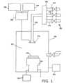
本明細書で開示される実施形態は、プラズマ支援式化学析出装置(即ち、PECVD装置、PEALD装置、又はPEPDL装置)に組み込まれることが好ましく、ただし、そのように限定はされない。図1は、本明細書で開示されるような実施形態を実現するように配置された様々な半導体基板プラズマ処理装置の構成要素を描いた簡易ブロック図を提供している。図に示されるように、半導体基板プラズマ処理装置300は、処理ゾーン内にプラズマを収容する働きをする真空チャンバ324を含み、プラズマは、上部RF電極(不図示)を中に有するシャワーヘッドモジュール314が、下部RF電極(不図示)を中に有する基板台座モジュール320と連携することによって生成することができる。真空チャンバ324内で半導体基板316の上面の上方の処理ゾーンに供給されるプロセスガスをプラズマ状態に活性化し、真空チャンバ324内でプラズマによる堆積プロセスが実施されえるように、少なくとも1つのRF発生器が、上記処理ゾーンにRFエネルギを供給するように動作可能である。例えば、整合回路網306に、高周波数RF発生器302及び低周波数RF発生器304がそれぞれ接続されてよく、整合回路網306は、真空チャンバ324内で半導体基板316の上方の処理ゾーンにRFエネルギが供給されえるように、シャワーヘッドモジュール314の上部RF電極に接続される。 Embodiments disclosed herein are preferably, but not limited to, incorporated into a plasma-enhanced chemical deposition apparatus (ie, a PECVD apparatus, a PEALD apparatus, or a PEPDL apparatus). FIG. 1 provides a simplified block diagram depicting various semiconductor substrate plasma processing apparatus components arranged to implement embodiments as disclosed herein. As shown, the semiconductor substrate
整合回路網306によって真空チャンバ324の内部に供給されるRFエネルギの電力及び周波数は、プロセスガスからプラズマを発生させるのに十分である。一実施形態では、高周波数RF発生器302及び低周波数RF発生器304の両方が使用され、代替の一実施形態では、高周波数RF発生器302のみが使用される。或るプロセスでは、高周波数RF発生器302は、約2~100MHzの周波数で動作されてよく、好ましい一実施形態では、13.56MHz又は27MHzで動作されてよい。低周波数RF発生器304は、約50kHzから2MHzで動作されてよく、好ましい一実施形態では、約350~600kHzで動作されてよい。プロセスパラメータは、チャンバ体積、基板サイズ、及びその他の要素に基づいて増減されてよい。同様に、プロセスガスの流量は、真空チャンバ又は処理ゾーンの自由体積によって決められてよい。 The power and frequency of the RF energy supplied to the interior of
基板台座モジュール320の上面は、真空チャンバ324内における処理時に半導体基板316を支持する。基板台座モジュール320は、半導体基板を保持するためのチャック、並びに/又は堆積プロセス及び/若しくはプラズマ処理プロセスの前、最中、及び/若しくは後に半導体基板を昇降させるためのリフトピンを含むことができる。代替の一実施形態では、基板台座モジュール320は、堆積プロセス及び/又はプラズマ処理プロセスの前、最中、及び/若しくは後に半導体基板を昇降させるためのキャリアリングを含むことができる。チャックは、静電式チャック、機械式チャック、又は産業及び/若しくは研究で使用可能であるその他の様々なタイプのチャックであってよい。静電式チャックを含む、基板台座モジュールのためのリフトピンアセンブリの詳細は、参照によって本明細書に全体を組み込まれる同一出願人による米国特許第8,840,754号で見受けられる。基板台座モジュールのためのキャリアリングの詳細は、参照によって本明細書に全体を組み込まれる同一出願人による米国特許第6,860,965号で見受けられる。裏側ガス供給部341は、基板台座モジュール320を通して半導体基板の下面の下方の領域に熱伝達ガス又はパージガスを供給するように動作可能である。基板台座モジュール320は、下部RF電極を中に含み、この下部RF電極は、処理時に接地されていることが好ましく、ただし、代替の一実施形態では、この下部RF電極は、処理時にRFエネルギを供給されてよい。 The top surface of
半導体基板プラズマ処理装置300の真空チャンバ324内で半導体基板を処理するために、プロセスガス源362から入口312及びシャワーヘッドモジュール314を通じて真空チャンバ324にプロセスガスが導入され、プロセスガスは、半導体基板の上面に膜が堆積されえるように、RFエネルギによってプラズマ状態にされる。一実施形態では、プロセスガス源362は、加熱されたマニホールド308に接続された複数のガスライン310を含むことができる。ガスは、事前に混合されてよい、又は別々にチャンバに供給されてよい。半導体基板処理時にシャワーヘッドモジュール314を通じて正しいガスが送られることを保証するために、適切な弁・質量流量制御メカニズムが用いられる。処理時には、基板台座モジュール320で支持されている半導体基板の下面の下方の領域に、裏側熱伝達ガス又はパージガスが供給される。好ましくは、処理は、化学気相成長処理、プラズマ支援式化学気相成長処理、原子層堆積処理、プラズマ支援式原子層堆積処理、パルス堆積層処理、又はプラズマ支援式パルス堆積層処理のうちの少なくとも1つである。 To process a semiconductor substrate in the
特定の実施形態では、堆積時に、堆積後処理時に、及び/又はその他のプロセス動作時におけるプロセス条件を制御するために、システムコントローラ162が用いられる。コントローラ162は、通常は、1つ以上の記憶装置と、1つ以上のプロセッサとを含む。プロセッサとしては、CPU又はコンピュータ、アナログ及び/又はデジタル入力/出力接続、ステッピングモータ制御盤などが挙げられる。 In certain embodiments, system controller 162 is used to control process conditions during deposition, post-deposition treatment, and/or other process operations. Controller 162 typically includes one or more storage devices and one or more processors. Processors include CPUs or computers, analog and/or digital input/output connections, stepper motor control boards, and the like.
特定の実施形態では、コントローラ162は、装置の全活動を制御する。システムコントローラ162は、処理動作のタイミング、低周波数RF発生器304及び高周波数RF発生器302の動作周波数及び動作出力、前駆体及び不活性ガス及びそれらの相対的混合物の流量及び温度、基板台座モジュール320の上面で支持される半導体基板316及びシャワーヘッドモジュール314のプラズマ照射表面の温度、真空チャンバ324の圧力、並びに特定のプロセスのその他のパラメータを制御するための命令一式を含むシステム制御ソフトウェアを実行する。実施形態によっては、コントローラに関係付けられた記憶装置に格納されたその他のコンピュータプログラムが用いられてよい。 In certain embodiments, controller 162 controls all device activities. The system controller 162 controls the timing of process operations, the operating frequencies and powers of the low
通常は、コントローラ162に、ユーザインターフェースが関係付けられている。ユーザインターフェースとしては、ディスプレイ画面、装置及び/又はプロセス条件のグラフィックソフトウェア表示、ポインティングデバイス、キーボード、タッチ画面、マイクロフォンなどのユーザ入力機器が挙げられる。 A user interface is typically associated with the controller 162 . User interfaces include display screens, graphical software representations of equipment and/or process conditions, user input devices such as pointing devices, keyboards, touch screens, microphones, and the like.
非一過性のコンピュータマシン読み取り可能媒体は、装置の制御のためのプログラム命令を含むことができる。処理動作を制御するためのコンピュータプログラムコードは、例えば、アセンブリ言語、C、C++、Pascal、Fortranなどの、従来の任意のコンピュータ読み取り可能プログラミング言語で記述することができる。プログラムに指定されたタスクを実施するために、コンパイル済みのオブジェクトコード又はスクリプトがプロセッサによって実行される。 A non-transitory computer machine readable medium may contain program instructions for control of the device. Computer program code for controlling processing operations may be written in any conventional computer-readable programming language, such as, for example, assembly language, C, C++, Pascal, Fortran, or the like. Compiled object code or scripts are executed by the processor to perform the tasks specified in the program.
コントローラパラメータは、例えば、処理工程のタイミング、前駆体及び不活性ガスの流量及び温度、半導体基板の温度、チャンバの圧力、及び特定のプロセスのその他のパラメータなどの、プロセス条件に関する。これらのパラメータは、レシピの形式でユーザに提供され、ユーザインターフェースを用いて入力されてよい。 Controller parameters relate to process conditions such as, for example, the timing of processing steps, precursor and inert gas flow rates and temperatures, semiconductor substrate temperature, chamber pressure, and other parameters for a particular process. These parameters may be provided to the user in the form of a recipe and entered using a user interface.
システムコントローラのアナログ及び/又はデジタル入力接続によって、プロセスを監視するための信号が提供されてよい。プロセスを制御するための信号は、装置のアナログ及びデジタル出力接続に載せて出力される。 Analog and/or digital input connections of the system controller may provide signals for monitoring the process. Signals for controlling the process are output on the analog and digital output connections of the device.
システムソフトウェアは、様々に設計又は構成されてよい。例えば、堆積プロセスを実施するために必要とされるチャンバ構成要素の動作を制御するために、様々なチャンバ構成要素サブルーチン又は制御オブジェクトが記述されてよい。これを目的としたプログラム又はプログラム部分の例として、基板処理段階のタイミングのコード、前駆体及び不活性ガスの流量及び温度のコード、並びに真空チャンバ324の圧力のためのコードが挙げられる。 System software may be designed or configured in various ways. For example, various chamber component subroutines or control objects may be written to control the operation of the chamber components required to perform a deposition process. Examples of programs or portions of programs intended for this purpose include code for timing of substrate processing steps, code for precursor and inert gas flow rates and temperatures, and code for
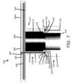
図2~7は、本明細書で開示される実施形態にしたがった基板台座モジュール320の断面を示している。図2~7に示されるように、基板台座モジュール320は、セラミック材料で作成された露出表面を有する保持板205を含む。保持板205は、半導体基板の処理時に半導体基板を支持するように動作可能である上面206を有する。セラミック材料で作成されたステム210が、保持板205の下面から下方に伸び、ステム210の上端214は、保持板205を支持する。好ましくは、ステム205の上端214は、保持板205のセラミック下面に接合(蝋付け、溶接、拡散接合、又はその他の適切な技術によって接合)される上方フランジ(突縁)を含む。基板台座モジュール320のステム210及び保持板205を、アルミニウム又はアルミニウム合金などの金属材料ではなくセラミック材料で作成することによって、基板台座モジュール320は、約550℃を超える温度又は約650℃を超える温度などの、高温基板処理時における高温に耐えられるだろう。 2-7 show cross-sections of a
保持板205は、少なくとも1つの静電把持電極209を埋め込まれて含むことができ、この少なくとも1つの静電把持電極209は、処理時に半導体基板を保持板205の上面206に静電的に把持するように動作可能である。図2及び図4~7に示されるように、保持板205は、下部RF電極265も含むことができ、この下部RF電極265は、半導体基板の処理時に接地されてよい、又はRF電力を供給されてよい。好ましくは、図3に示されるように、保持板205は、静電把持電極及びRF電極の両方として機能する単極209aのみを埋め込まれて含む。図2~7に戻り、保持板205は、処理時に保持板205の上面206全域の温度を及びそれによって半導体基板全域の温度を制御するように動作可能である少なくとも1つのヒータ260を埋め込まれて含むこともできる。少なくとも1つのヒータ260は、電気抵抗性のヒータ膜、及び/又は1つ以上の熱電モジュールを含むことができる。好ましくは、少なくとも1つの静電把持電極209、少なくとも1つのヒータ260、単極209a、及び/又は下部RF電極265への電気的接続が、ステム210の側壁211によって画定されたステム210の円筒状内部領域216内に配される。これらの電気的接続は、保持板205内に形成された、対応する少なくとも1つの静電把持電極209、少なくとも1つのヒータ260、単極209a、及び/又は下部RF電極265と電気的に連絡している電気的接触(不図示)に、それぞれ接続されてよい。このように、少なくとも1つの静電把持電極209、少なくとも1つのヒータ260、単極209a、及び/又は下部RF電極265は、半導体基板の処理時に通電されてよい。 The
一実施形態では、保持板205は、拡散接合によって貼り合わされた個々の層を含むことができ、保持板205のこれらの個々の層間には、少なくとも1つの静電把持電極209、下部RF電極265(又は単極209a)、及び少なくとも1つのヒータ260が挟まれることができる。保持板205の上面206は、メサパターン206aを中に形成されて含むことが好ましく、半導体基板の下面は、このメサパターン206a上で支持され、半導体基板の下方におけるメサパターン206aのメサ間領域には、裏側パージガス又は裏側熱伝達ガスを供給することができる。メサパターン及びその形成方法の代表的な一実施形態は、参照によってその全体を本明細書に組み込まれる同一出願人による米国特許第7,869,184号で見受けられる。一実施形態では、基板台座モジュール320は、保持板205の上部とステム210との間における熱伝達を抑制するように動作可能である熱遮蔽(不図示)を含むことができる。熱遮蔽を含む基板台座モジュールの代表的な一実施形態は、参照によってその全体を本明細書に組み込まれる同一出願人による米国特許第8,753,447号で見受けられる。 In one embodiment, the
保持板205の露出表面及びステム210は、セラミック材料で作成されることが好ましく、このような材料は、保持板205及びステム210が処理条件に曝される処理時に基板の汚染を招かないことが好ましいとされる。好ましくは、保持板205の露出表面及びステム210は、窒化アルミニウムで作成される。 The exposed surface of
ステム210は、基板台座モジュール320が半導体基板処理装置の真空チャンバ内で支持可能であるように、アダプタ220の上面223に装着された下面213を含む。アダプタ220は、円筒状内部領域225を画定する側壁221を有する。ステム210の下面213は、ステム210の側壁211内に位置付けられた対応するガス通路217と流体連通している少なくとも1つのガス入口216を含む。ステム210の、少なくとも1つのガス入口216は、アダプタ220の上面223内の少なくとも1つのガス出口224と流体連通しており、この少なくとも1つのガス出口224は、アダプタ220の側壁221内の対応するガス通路232と流体連通している。保持板205は、ステム210の側壁211内の対応するガス通路217と流体連通している少なくとも1本の保持板ガス通路280を含む。裏側ガスは、半導体基板の処理時において、アダプタ220の側壁221内の少なくとも1本のガス通路232と流体連通している裏側ガス供給部から、保持板205の上面206で支持されている半導体基板の下方の領域に、ステム210の少なくとも1本のガス通路217を通じて供給されてよい。
次に、図2、図5、及び図6を参照すると、アダプタ220の上面223内の少なくとも1つのガス出口224は、アダプタ220の上面223内の環状ガス流路242内に位置付けられることが好ましい。本明細書で言う「環状ガス流路」は、切れ目のない環状経路を形成するガス流路、環状経路の一部に沿って伸びるガス流路、又は共通の中心点を有するそれぞれの環状経路に沿って伸びる互いに流体的に隔離された2本以上のガス流路を意味することができる。アダプタ220の上面223は、また、少なくとも1つのガス出口224の半径方向内側に位置付けられた内側溝226と、この内側溝226の半径方向外側に位置付けられた外側溝227とを含む。内側溝226は、半導体基板の処理時にアダプタ220の円筒状内部領域225と少なくとも1つのガス出口224との間に内側真空シールを形成するように、内側Oリング230を中に有する。外側溝227は、半導体基板の処理時にアダプタ220の側壁221の周囲領域と少なくとも1つのガス出口224との間の領域に外側真空シールを形成するように、外側Oリング231を中に有する。 2, 5 and 6, at least one
次に、図5及び図6を参照すると、アダプタ220の上面223内の環状ガス流路242は、アダプタ220の外側溝227の半径方向内側の部分に形成されることが好ましく、外側Oリング231は、外側溝227の半径方向外側の部分に配置される。 5 and 6, an
図3、図4、及び図7に示されるような、代替の一実施形態では、アダプタ220の上面223内の環状ガス流路242(図2を参照)の代わり又は追加として、ステム210の下面213に環状ガス流路252が含められる。アダプタ220の少なくとも1つのガス出口224は、ステム210の下面213内の環状ガス流路252と流体連通している。ステム210の下面213内の少なくとも1つのガス入口216は、ステム210の下面213内に形成された環状ガス流路252内に位置付けられる。ステム210の下面213が環状ガス流路252を含みアダプタ220の上面223が環状ガス流路242を含む一実施形態では、環状ガス流路242、252は、流体連通するように互いに隣り合うように配置される。 In an alternative embodiment, as shown in FIGS. 3, 4, and 7, instead of or in addition to annular gas passage 242 (see FIG. 2) in
図3を参照すると、アダプタ220の上面223は、少なくとも1つのガス出口224の半径方向内側に位置付けられた内側溝226と、この内側溝226の半径方向外側に位置付けられた外側溝227とを含むことが好ましい。内側溝226は、半導体基板の処理時にアダプタ220の円筒状内部領域225と少なくとも1つのガス出口224との間に内側真空シールを形成するように、内側Oリング230を中に有する。外側溝227は、半導体基板の処理時にアダプタ220の側壁221の周囲領域と少なくとも1つのガス出口224との間の領域に外側真空シールを形成するように、外側Oリング231を中に有する。 Referring to FIG. 3, the
次に、図4を参照すると、ステム210の下面213は、アダプタ220の上面223内の内側溝226及び外側溝227(図2を参照)の代わり又は追加として、内側溝250及び外側溝251を含むことができる。内側溝250は、半導体基板の処理時にアダプタ220の円筒状内部領域225と少なくとも1つのガス出口224との間に内側真空シールを形成するように、内側Oリング230を中に有する。外側溝251は、半導体基板の処理時にアダプタ220の側壁221の周囲領域と少なくとも1つのガス出口224との間の領域に外側真空シールを形成するように、外側Oリング231を中に有する。ステム210の下面213が内側溝250及び外側溝251を含み、アダプタ220の上面223が内側溝226及び外側溝227を含む一実施形態では、内側溝250、226は、内側溝250、226のそれぞれの中に内側Oリング230の一部が含まれるように、互いに隣り合うように配置されることが好ましく、外側溝251、227は、外側溝251、227のそれぞれの中に外側Oリング231の一部が含まれるように、互いに隣り合うように配置されることが好ましい。 4, the
次に、図7を参照すると、ステム210の下面213内の環状ガス流路252は、ステム210の外側溝251の半径方向内側の部分に形成されることが好ましく、外側Oリング231は、外側溝251の半径方向外側の部分に配置されることが好ましい。 Referring now to FIG. 7, an
次に、図2~7を参照すると、ステム210は、ステム210の側壁211から外向きに延びる下方外側フランジ234の上方におけるステム210の側壁211の厚さが最小限に抑えられて、処理時に保持板205とステム210の下面213との間に熱的な絞りが形成されえるように、下方外側フランジ234を含むことが好ましい。下方外側フランジ234は、基板台座モジュール320のステム210がボルトやネジなどの締め具によってアダプタ220の上面223に装着されえるように、通し穴(不図示)を含むことができる。ステム210の円筒状内部215内及びアダプタ220の円筒状内部225内が正圧に維持されえるように、処理時において、円筒状内部215、225は、流体連通しており、内側Oリング230及び外側Oリング231によって真空環境から密閉されている。円筒状内部領域215、225は、大気に曝されていることが好ましいが、代替の一実施形態では、円筒状内部領域215,225内に不活性ガス又はパージガスがポンプによって投入されてよい。 2-7, stem 210 is configured such that the thickness of
ステム210は、セラミックで形成され、好ましくは、保持板205から、内側Oリング230及び外側Oリング231が位置するステム210の下面213とアダプタ220の上面223との間の境界への熱の伝達を軽減するために、低い熱伝導率を有する。この境界は、低めの温度(例えば、約200℃から約300℃)に維持されることが望ましい。例えば、内側Oリング230及び外側Oリング231は、処理時に曝される温度が高すぎると、機能しなくなり、ステム210の円筒状内部領域215とステム210の側壁211の周囲(真空)領域との間にシールを形成しなくなる。ステム210の側壁211の厚さを薄くすることを可能にする下方外側フランジ234に加えて、ステム210は、ステム210の側壁211から内向きに延びる下方内側フランジ233の上方におけるステム210の側壁211の厚さが最小限に抑えられ、半導体基板の処理時に保持板205とステム210の下面213との間に熱的な絞りが形成されえるように、下方内側フランジ233を含むことが好ましい(図2~4、図6、及び図7を参照)。
ステム210の側壁211の厚さは、半導体基板の処理時にステム210の側壁211が保持板205とステム210の下面213との間に熱的な絞りを形成するように、アダプタ220の側壁221の厚さ未満であることが好ましい。一実施形態では、ステム210の下方フランジの上方におけるステム210の側壁211の厚さは、約3mm以下であり、より好ましくは、約2mm以下である。好ましい一実施形態では、ステム210の側壁211の厚さは、好ましくは大気圧に維持されるその円筒状内部領域215と半導体基板の処理時に減圧又は真空圧で運転される側壁211の周囲領域との間における圧力差にステム210が耐えるために必要とされる最小の厚さを僅かに超える厚さであるように選択される。 The thickness of
アダプタ220は、アルミニウム又はアルミニウム合金などの金属で形成されることが好ましく、このような材料は、ステム210及び保持板205を形成するために使用される高純度セラミックよりも安価な材料であり、また、処理時に及ぼされる高い圧力差のもとでも壊れにくい。したがって、ステム210の側壁211からの熱的な絞りを形成することによって、保持板205の上面206で支持されている半導体ウエハを処理するために使用される高温(例えば、550℃~650℃又はそれ以上)が、ステム210の下面213から熱的に隔離されえて、したがって、ステム210は、アルミニウム又はアルミニウム合金のアダプタ220の上面223に装着されてよく、Oリング230、231が、高温ゆえに機能しなくなることはないだろう。更に、ステム210の側壁211を熱的な絞りであるように形成することによって、保持板205と下面213との間におけるステム210の長さを短くすること及びアダプタ220の長さを長くすることが可能になり、それによって、材料費が節約される。
図6に示されるように、アダプタ220は、その側壁221内に、アダプタ220の上面223内の環状ガス流路242を通じてステム210の側壁211内の少なくとも2本のガス通路217と流体連通している1本のガス通路232を含むことができ、ステム210の側壁211内の各ガス通路217は、保持板の上面で支持されている半導体基板の下方の領域に処理時に裏側ガス供給部によって裏側ガスが供給されえるように、対応する保持板ガス通路280と流体連通している。 As shown in FIG. 6,
更なる一実施形態では、アダプタ220の少なくとも1つのガス出口224を、ステム210の、対応する少なくとも1つのガス入口216の1つ以上と位置を揃える又は位置をずらすことができる。例えば、アダプタ220は、その側壁221内に、アダプタ220の上面223内の環状ガス流路242を通じてステム210の側壁211内の少なくとも1本のガス通路217と流体連通している少なくとも1本のガス通路232を含むことができ、アダプタ220の側壁221内の少なくとも1本のガス通路232の少なくとも1つの対応するガス出口224は、ステム210の側壁211内の少なくとも1本のガス通路217の少なくとも1つのガス入口216と位置を揃えられる。或いは、アダプタ220は、その側壁221内に、アダプタ220の上面223内の環状ガス流路242を通じてステム210の側壁211内の少なくとも1本のガス通路217と流体連通している少なくとも1本のガス通路232を含むことができ、アダプタ220の側壁221内の少なくとも1本のガス通路232の少なくとも1つの対応するガス出口224は、ステム210の側壁211内の少なくとも1本のガス通路217の少なくとも1つの対応するガス入口216と位置をずらされる。 In a further embodiment, at least one
等温処理ゾーンを含むプラズマ処理装置が、その具体的な実施形態を参照にして詳細に説明されてきたが、当業者にならば、添付の特許請求の範囲から逸脱することなく様々な変更及び修正を加えること並びに均等物を採用することができることが、明らかである。
本発明は、例えば、以下のような形態で実現することもできる。
[形態1]
ステムの下面と、前記ステムを支持するアダプタの上面との間に最小化された装着面積を有する高温基板台座モジュールを含む、半導体基板を処理するための半導体基板処理装置であって、
半導体基板が処理されえる処理ゾーンを含む真空チャンバと、
プロセスガス源からのプロセスガスが通って前記真空チャンバの前記処理ゾーンに供給されるシャワーヘッドモジュールと、
基板台座モジュールであって、
処理時に半導体基板を支持するように構成された上面を有する保持板と、
円筒状内部領域を画定する側壁、下面、及び、前記保持板を支持する上端を有するセラミック材料のステムと、
円筒状内部領域を画定する側壁、及び、前記ステムの前記下面に装着される上面を有するアダプタと、
を含む基板台座モジュールと、
を備え、
前記ステムの前記下面は、前記ステムの前記側壁内に位置付けられた対応するガス通路と流体連通している少なくとも1つのガス入口を含み、前記少なくとも1つのガス入口は、前記アダプタの前記上面内の環状ガス流路内に位置付けられた少なくとも1つのガス出口と流体連通しており、前記アダプタの前記上面は、前記少なくとも1つのガス出口の半径方向内側に位置付けられた内側溝と、前記内側溝の半径方向外側に位置付けられた外側溝とを含み、前記内側溝は、処理時に前記アダプタの前記円筒状内部領域と前記少なくとも1つのガス出口との間に内側真空シールを形成するように、内側Oリングを中に有し、前記外側溝は、処理時に前記アダプタの前記側壁の周囲領域と前記少なくとも1つのガス出口との間の領域に外側真空シールを形成するように、外側Oリングを中に有し、
前記保持板は、前記ステムの前記側壁内の対応するガス通路と流体連通している少なくとも1本の保持板ガス通路を含み、裏側ガスは、前記保持板ガス通路を通して、前記保持板の前記上面で支持されている半導体基板の下方の領域に処理時に供給することができる、半導体基板処理装置。
[形態2]
形態1に記載の半導体基板処理装置であって、
前記アダプタの前記上面内の前記環状ガス流路は、前記アダプタの前記外側溝の半径方向内側の部分に形成され、前記外側Oリングは、前記外側溝の半径方向外側の部分に配置される、半導体基板処理装置。
[形態3]
形態1に記載の半導体基板処理装置であって、
(a)前記ステムの前記下面は、前記アダプタの前記上面内の前記環状ガス流路に隣接する環状ガス流路を含み、前記ステムの前記少なくとも1つのガス入口は、前記アダプタの前記上面内の前記環状ガス流路及び前記ステムの前記下面内の前記環状ガス流路と流体連通している、又は
(b)前記ステムの前記下面は、前記アダプタの前記内側溝に隣接する内側溝を含み、前記内側Oリングの一部が、前記ステムの前記内側溝内にあり、前記ステムの前記下面は、前記アダプタの前記外側溝に隣接する外側溝を含み、前記外側Oリングの一部が、前記ステムの前記外側溝内にある、又は
(c)前記ステムの前記下面は、前記アダプタの前記内側溝に隣接する内側溝を含み、前記内側Oリングの一部が、前記ステムの前記内側溝内にあり、前記ステムの前記下面は、前記アダプタの前記外側溝に隣接する外側溝を含み、前記外側Oリングの一部が、前記ステムの前記外側溝内にあり、前記ステムの前記下面は、更に、前記アダプタの前記上面内の前記環状ガス流路に隣接する環状ガス流路を含み、前記ステムの前記少なくとも1つのガス入口は、前記ステムの前記環状ガス流路内にあり、前記ステムの前記環状ガス流路は、前記アダプタの前記環状ガス流路と流体連通している、又は
(d)前記ステムの前記下面は、前記アダプタの前記内側溝に隣接する内側溝を含み、前記内側Oリングの一部が、前記ステムの前記内側溝内にあり、前記ステムの前記下面は、前記アダプタの前記外側溝に隣接する外側溝を含み、前記外側Oリングの一部が、前記ステムの前記外側溝内にあり、前記ステムの前記少なくとも1つのガス入口は、前記ステムの前記外側溝の半径方向内側の部分に位置付けられ、前記ステムの前記外側溝の前記半径方向内側の部分は、前記アダプタの前記環状ガス流路と流体連通している環状ガス流路を形成し、前記外側Oリングは、前記ステムの前記外側溝の半径方向外側の部分にある、半導体基板処理装置。
[形態4]
形態1に記載の半導体基板処理装置であって、
前記半導体基板処理装置は、
(a)前記処理ゾーン内で前記プロセスガスをプラズマ状態に活性化するように適応されたRFエネルギ源、
(b)前記半導体基板処理装置によって実施されるプロセスを制御するように構成された制御システム、及び/又は
(c)前記半導体基板処理装置の制御のためのプログラム命令を含む非一過性のコンピュータマシン読み取り可能媒体
を含む、半導体基板処理装置。
[形態5]
形態1に記載の半導体基板処理装置であって、
(a)前記ステムは、前記ステムの前記側壁から内向きに延びる下方内側フランジであって、前記下方内側フランジの上方における前記ステムの前記側壁の厚さが、処理時に前記保持板と前記ステムの前記下面との間に熱的な絞りを形成するように構成された下方内側フランジを含む、及び/又は
(b)前記ステムは、前記ステムの前記側壁から外向きに延びる下方外側フランジであって、前記下方外側フランジの上方における前記ステムの前記側壁の厚さが、処理時に前記保持板と前記ステムの前記下面との間に熱的な絞りを形成するように構成された下方外側フランジを含む、半導体基板処理装置。
[形態6]
形態1に記載の半導体基板処理装置であって、
(a)前記ステムの前記側壁の厚さは、前記ステムの前記側壁が処理時に前記保持板と前記ステムの前記下面との間に熱的な絞りを形成するように、前記アダプタの前記側壁の厚さ未満である、
(b)前記ステムの下方フランジの上方における前記ステムの前記側壁の厚さは、約3mm以下若しくは約2mm以下である、
(c)前記アダプタは、アルミニウム若しくはアルミニウム合金で作成される、及び/又は
(d)前記保持板の露出表面は、セラミック材料で作成される、
半導体基板処理装置。
[形態7]
形態1に記載の半導体基板処理装置であって、
前記高温基板台座モジュールは、更に、
(a)前記保持板に埋め込まれた少なくとも1つの静電把持電極、
(b)前記保持板に埋め込まれた底部RF電極、
(c)前記保持板に埋め込まれたヒータ、
(d)前記保持板の前記上面に対して半導体基板を昇降させるように構成されたキャリアリング、
(e)前記保持板の前記上面に対して半導体基板を昇降させるように構成された複数のリフトピン、又は
(f)前記高温基板台座モジュールに埋め込まれ、静電把持電極及びRF電極として機能するように動作可能である単極、
を含む、半導体基板処理装置。
[形態8]
形態1に記載の半導体基板処理装置であって、
(a)前記アダプタは、その側壁内に、前記アダプタの前記上面内の前記環状ガス流路を通じて前記ステムの前記側壁内の少なくとも2本のガス通路と流体連通している1本のガス通路を含み、前記ステムの前記側壁内の各ガス通路は、前記保持板の前記上面で支持されている半導体基板の下方の領域に処理時に裏側ガスが供給されえるように、対応する保持板ガス通路と流体連通している、及び/又は
(b)前記アダプタは、その側壁内に、前記アダプタの前記上面内の前記環状ガス流路を通じて前記ステムの前記側壁内の少なくとも1本のガス通路と流体連通している少なくとも1本のガス通路を含み、前記アダプタの前記側壁内の前記少なくとも1本のガス通路の少なくとも1つの対応するガス出口は、前記ステムの前記側壁内の前記少なくとも1本のガス通路の少なくとも1つの対応するガス入口と位置を揃えられる、若しくは前記アダプタの前記対応するガス出口は、前記ステムの前記対応するガス入口と位置をずらされる、半導体基板処理装置。
[形態9]
形態1に記載の半導体基板処理装置であって、更に、
前記保持板の前記上面で支持されている半導体基板の下方の領域に前記ステムの前記側壁を通して処理時に裏側熱伝達ガス又はパージガスが供給されえるように、前記アダプタの前記側壁内に位置付けられた少なくとも1本のガス通路に裏側熱伝達ガス又はパージガスを供給するように動作可能である裏側ガス供給部を備える半導体基板処理装置。
[形態10]
半導体基板処理装置の高温基板台座モジュールであって、
処理時に半導体基板を支持するように構成された上面を有する保持板と、
円筒状内部領域を画定する側壁、下面、及び前記保持板を支持する上端を有するステムであって、前記ステムの前記下面は、アダプタの上面に装着されるように構成される、ステムと、
を備え、
前記ステムの前記下面は、少なくとも1つのガス入口を中に有する環状ガス流路を含み、前記少なくとも1つのガス入口は、前記ステムの前記側壁内に位置付けられた対応するガス通路と流体連通しており、前記ステムの前記下面内の前記少なくとも1つのガス入口は、前記ステムがアダプタに装着されるときに前記アダプタの上面内の少なくとも1つのガス出口と流体連通するように構成され、
前記保持板は、前記ステムの前記側壁内の対応するガス通路と流体連通している少なくとも1本の保持板ガス通路を含み、裏側ガスは、前記保持板ガス通路を通して、前記保持板の前記上面で支持されている半導体基板の下方の領域に処理時に供給することができる、高温基板台座モジュール。
[形態11]
形態10に記載の高温基板台座モジュールであって、更に、
(a)前記ステムの前記下面が上面に装着されるアダプタであって、前記アダプタの前記上面は、前記ステムの前記少なくとも1つのガス入口と流体連通している少なくとも1つのガス出口を有する環状ガス流路と、前記少なくとも1つのガス出口の半径方向内側にある内側溝であって、前記内側溝内に、処理時に前記ステムの前記円筒状内部領域と前記ステムの前記下面内の前記少なくとも1つのガス入口との間に内側真空シールを形成するように内側Oリングがある内側溝と、前記内側溝の半径方向外側にある外側溝であって、前記外側溝内に、処理時に前記ステムの前記側壁の周囲領域と前記ステムの前記下面内の前記少なくとも1つのガス入口との間に外側真空シールを形成するように外側Oリングがある外側溝とを含む、アダプタ、
(b)前記ステムの前記下面が上面に装着されるアダプタであって、前記アダプタの前記上面は、前記ステムの前記少なくとも1つのガス入口と流体連通している少なくとも1つのガス出口と、前記少なくとも1つのガス出口の半径方向内側にある内側溝であって、前記内側溝内に、処理時に前記ステムの前記円筒状内部領域と前記ステムの前記少なくとも1つのガス入口との間に内側真空シールを形成するように内側Oリングがある内側溝と、前記内側溝の半径方向外側にある外側溝であって、前記外側溝内に、処理時に前記ステムの前記側壁の周囲領域と前記ステムの前記少なくとも1つのガス入口との間に外側真空シールを形成するように外側Oリングがある外側溝とを含む、アダプタ、
(c)前記ステムの前記下面が上面に装着されるアダプタであって、前記アダプタの前記上面は、前記ステムの前記少なくとも1つのガス入口と流体連通している少なくとも1つのガス出口を有する環状ガス流路と、前記少なくとも1つのガス出口の半径方向内側にある内側溝であって、前記内側溝内に、処理時に前記ステムの前記円筒状内部領域と前記ステムの前記下面内の前記少なくとも1つのガス入口との間に内側真空シールを形成するように内側Oリングがある内側溝と、前記内側溝の半径方向外側にある外側溝であって、前記外側溝内に、処理時に前記ステムの前記側壁の周囲領域と前記ステムの前記下面内の前記少なくとも1つのガス入口との間に外側真空シールを形成するように外側Oリングがある外側溝とを含み、前記ステムの前記下面は、前記アダプタの前記内側溝に隣接する内側溝と、前記アダプタの前記外側溝に隣接する外側溝とを含み、前記ステムの前記内側溝は、前記内側Oリングの一部を中に含み、前記ステムの前記外側溝は、前記外側Oリングの一部を中に含む、アダプタ、又は
(d)前記ステムの前記下面が上面に装着されるアダプタであって、前記アダプタの前記上面は、前記ステムの前記少なくとも1つのガス入口と流体連通している少なくとも1つのガス出口と、前記少なくとも1つのガス出口の半径方向内側にある内側溝であって、前記内側溝内に、処理時に前記ステムの前記円筒状内部領域と前記ステムの前記少なくとも1つのガス入口との間に内側真空シールを形成するように内側Oリングがある内側溝と、前記内側溝の半径方向外側にある外側溝であって、前記外側溝内に、処理時に前記ステムの前記側壁の周囲領域と前記ステムの前記少なくとも1つのガス入口との間に外側真空シールを形成するように外側Oリングがある外側溝とを含み、前記ステムの前記下面は、前記アダプタの前記内側溝に隣接する内側溝と、前記アダプタの前記外側溝に隣接する外側溝とを含み、前記ステムの前記内側溝は、前記内側Oリングの一部を中に含み、前記ステムの前記外側溝は、前記外側Oリングの一部を中に含む、アダプタ
を備える高温基板台座モジュール。
[形態12]
形態10に記載の高温基板台座モジュールであって、
(a)前記ステムの前記下面は、処理時に前記ステムの前記円筒状内部領域と前記少なくとも1つのガス入口との間に内側真空シールを形成するように、前記アダプタの前記上面に前記ステムの前記下面が装着されるときに内側Oリングを中に含むように構成された、前記少なくとも1つのガス入口の半径方向内側にある内側溝と、処理時に前記ステムの前記側壁の周囲領域と前記少なくとも1つのガス入口との間に外側真空シールを形成するように、前記アダプタの前記上面に前記ステムの前記下面が装着されるときに外側Oリングを含むように構成された、前記少なくとも1つのガス入口の半径方向外側にある外側溝とを含む、又は
(b)前記ステムの前記下面は、処理時に前記ステムの前記円筒状内部領域と前記少なくとも1つのガス入口との間に内側真空シールを形成するように、前記アダプタの前記上面に前記ステムの前記下面が装着されるときに内側Oリングを中に含むように構成された、前記少なくとも1つのガス入口の半径方向内側にある内側溝と、処理時に前記ステムの前記側壁の周囲領域と前記少なくとも1つのガス入口との間に外側真空シールを形成するように、前記アダプタの前記上面に前記ステムの前記下面が装着されるときに外側Oリングを含むように構成された、前記少なくとも1つのガス入口の半径方向外側にある外側溝とを含み、前記ステムの前記環状ガス流路は、前記ステムの前記外側溝の半径方向内側の部分に形成され、前記外側Oリングは、前記ステムが前記アダプタに装着されるときに前記外側溝の半径方向外側の部分にあるように構成される、高温基板台座モジュール。
[形態13]
形態10に記載の高温基板台座モジュールであって、
(a)前記ステムは、前記ステムの前記側壁から内向きに延びる下方内側フランジであって、前記下方内側フランジの上方における前記ステムの前記側壁の厚さが、処理時に前記保持板と前記ステムの前記下面との間に熱的な絞りを形成するように構成された下方内側フランジを含む、及び/又は
(b)前記ステムは、前記ステムの前記側壁から外向きに延びる下方外側フランジであって、前記下方外側フランジの上方における前記ステムの前記側壁の厚さが、処理時に前記保持板と前記ステムの前記下面との間に熱的な絞りを形成するように構成された下方外側フランジを含む、高温基板台座モジュール。
[形態14]
形態10に記載の高温基板台座モジュールであって、
(a)前記ステムの前記側壁の厚さは、前記ステムの前記側壁が処理時に前記保持板と前記ステムの前記下面との間に熱的な絞りを形成するように、前記ステムが装着されえる前記アダプタの前記側壁の厚さ未満であるように構成される、
(b)前記ステムの下方フランジの上方における前記ステムの前記側壁の厚さは、約3mm以下若しくは約2mm以下である、及び/又は
(c)前記保持板の露出表面は、セラミック材料で作成される、高温基板台座モジュール。
[形態15]
形態10に記載の高温基板台座モジュールであって、
前記高温基板台座モジュールは、更に、
(a)前記保持板に埋め込まれた少なくとも1つの静電把持電極、
(b)前記保持板に埋め込まれた底部RF電極、
(c)前記保持板に埋め込まれたヒータ、
(d)前記保持板の前記上面に対して半導体基板を昇降させるように構成されたキャリアリング、
(e)前記保持板の前記上面に対して半導体基板を昇降させるように構成された複数のリフトピン、又は
(f)前記高温基板台座モジュールに埋め込まれ、静電把持電極及びRF電極として機能するように動作可能である単極
を含む、高温基板台座モジュール。
[形態16]
半導体基板処理装置の高温基板台座モジュールのアダプタであって、前記半導体基板処理装置の真空チャンバ内で前記基板台座モジュールのステムを支持するように構成され、前記アダプタは、
前記アダプタの円筒状内部領域を画定する側壁と、ステムの下面に装着されるように構成された上面と、を備え、
前記アダプタの前記上面は、前記アダプタの前記側壁内に位置付けられた対応するガス通路と流体連通している少なくとも1つのガス出口を含む環状ガス流路を含み、
前記少なくとも1つのガス出口は、前記アダプタの前記上面が前記ステムの下面に装着されるときに前記ステムの前記下面内の少なくとも1つのガス入口と流体連通するように構成され、
前記アダプタの前記上面は、前記少なくとも1つのガス出口の半径方向内側に位置付けられた内側溝と、前記内側溝の半径方向外側に位置付けられた外側溝とを含み、
前記内側溝は、処理時に前記アダプタの前記円筒状内部領域と前記少なくとも1つのガス出口との間に内側真空シールが形成されるように、前記アダプタが前記ステムに装着されるときに内側Oリングを中に含むように構成され、
前記外側溝は、処理時に前記アダプタの前記側壁の周囲領域と前記少なくとも1つのガス出口との間の領域に外側真空シールが形成されるように、前記アダプタが前記ステムに装着されるときに外側Oリングを中に含むように構成される、アダプタ。
[形態17]
形態16に記載のアダプタであって、
前記アダプタの前記上面内の前記環状ガス流路は、前記アダプタの前記外側溝の半径方向内側の部分に形成され、前記外側Oリングは、前記外側溝の半径方向外側の部分に配置される、アダプタ。
[形態18]
形態1に記載の半導体基板処理装置内で半導体基板を処理する方法であって、
前記プロセスガス源から前記処理ゾーン内へ前記プロセスガスを供給することと、
前記保持板の前記上面で支持されている半導体基板を処理することであって、前記ステムの前記少なくとも1本のガス通路を通じて前記アダプタの少なくとも1本のガス通路と流体連通している前記少なくとも1本の保持板ガス通路を通して裏側熱伝達ガス又はパージガスを供給することを含み、前記裏側ガスは、処理されている前記半導体基板の下方の領域に供給される、ことと、
を備える方法。
[形態19]
形態18に記載の方法であって、
前記保持板の前記上面は、少なくとも約600℃の温度であり、前記ステムと前記アダプタとの間の境界は、約300℃未満の温度である、方法。
[形態20]
形態18に記載の方法であって、
前記処理は、化学気相成長、プラズマ支援式化学気相成長、原子層堆積、プラズマ支援式原子層堆積、パルス堆積層、及び/又はプラズマ支援式パルス堆積層のうちの少なくとも1つである、方法。Although a plasma processing apparatus including an isothermal processing zone has been described in detail with reference to specific embodiments thereof, various changes and modifications will occur to those skilled in the art without departing from the scope of the appended claims. can be added as well as equivalents can be employed.
The present invention can also be implemented in the following forms, for example.
[Mode 1]
A semiconductor substrate processing apparatus for processing semiconductor substrates, comprising a high temperature substrate pedestal module having a minimized mounting area between a bottom surface of a stem and a top surface of an adapter supporting the stem, comprising:
a vacuum chamber containing a processing zone in which a semiconductor substrate can be processed;
a showerhead module through which process gas from a process gas source is supplied to the processing zone of the vacuum chamber;
A substrate pedestal module,
a retainer plate having a top surface configured to support a semiconductor substrate during processing;
a stem of ceramic material having sidewalls defining a cylindrical interior region, a lower surface, and an upper end supporting the retainer plate;
an adapter having a sidewall defining a cylindrical interior region and an upper surface attached to the lower surface of the stem;
a substrate pedestal module comprising
with
The lower surface of the stem includes at least one gas inlet in fluid communication with a corresponding gas passage located in the side wall of the stem, the at least one gas inlet in the upper surface of the adapter. in fluid communication with at least one gas outlet positioned within an annular gas flow path, the top surface of the adapter having an inner groove positioned radially inward of the at least one gas outlet; an outer groove positioned radially outwardly, said inner groove forming an inner vacuum seal between said cylindrical interior region of said adapter and said at least one gas outlet during processing. a ring therein, said outer groove having an outer O-ring therein so as to form an outer vacuum seal in an area between a peripheral region of said sidewall of said adapter and said at least one gas outlet during processing. have
The retainer plate includes at least one retainer plate gas passageway in fluid communication with a corresponding gas passageway in the side wall of the stem, backside gas passing through the retainer plate gas passageway to the upper surface of the retainer plate. A semiconductor substrate processing apparatus capable of supplying a region under a semiconductor substrate for processing during processing.
[Mode 2]
The semiconductor substrate processing apparatus according to Embodiment 1,
the annular gas passage in the upper surface of the adapter being formed in a radially inner portion of the outer groove of the adapter, and the outer O-ring being disposed in a radially outer portion of the outer groove; Semiconductor substrate processing equipment.
[Form 3]
The semiconductor substrate processing apparatus according to Embodiment 1,
(a) the lower surface of the stem includes an annular gas passage adjacent to the annular gas passage in the upper surface of the adapter, and the at least one gas inlet of the stem is within the upper surface of the adapter; in fluid communication with the annular gas passageway and the annular gas passageway in the lower surface of the stem; or
(b) the lower surface of the stem includes an inner groove adjacent to the inner groove of the adapter, a portion of the inner O-ring being within the inner groove of the stem, and the lower surface of the stem comprising: an outer groove adjacent to the outer groove of the adapter, a portion of the outer O-ring being within the outer groove of the stem; or
(c) the lower surface of the stem includes an inner groove adjacent to the inner groove of the adapter, a portion of the inner O-ring being within the inner groove of the stem, and the lower surface of the stem comprising: an outer groove adjacent to the outer groove of the adapter, a portion of the outer O-ring being within the outer groove of the stem; an annular gas passage adjacent to the annular gas passage, wherein the at least one gas inlet of the stem is within the annular gas passage of the stem; and the annular gas passage of the stem extends into the adapter. in fluid communication with said annular gas passage, or
(d) the lower surface of the stem includes an inner groove adjacent to the inner groove of the adapter, a portion of the inner O-ring being within the inner groove of the stem, the lower surface of the stem comprising: an outer groove adjacent to the outer groove of the adapter, a portion of the outer O-ring being within the outer groove of the stem, and the at least one gas inlet of the stem being in the outer groove of the stem; said radially inner portion of said outer groove of said stem forming an annular gas passageway in fluid communication with said annular gas passageway of said adapter, said outer O The semiconductor substrate processing apparatus, wherein the ring is radially outward of the outer groove of the stem.
[Mode 4]
The semiconductor substrate processing apparatus according to Embodiment 1,
The semiconductor substrate processing apparatus is
(a) an RF energy source adapted to activate the process gas to a plasma state within the processing zone;
(b) a control system configured to control processes performed by the semiconductor substrate processing apparatus; and/or
(c) a non-transitory computer machine readable medium containing program instructions for control of said semiconductor substrate processing apparatus;
A semiconductor substrate processing apparatus comprising:
[Mode 5]
The semiconductor substrate processing apparatus according to Embodiment 1,
(a) the stem has a lower inner flange extending inwardly from the sidewall of the stem, wherein the thickness of the sidewall of the stem above the lower inner flange is such that the thickness of the sidewall of the stem above the lower inner flange is such that the thickness of the retainer plate and the stem during processing; including a lower inner flange configured to form a thermal restriction with said lower surface; and/or
(b) the stem has a lower outer flange extending outwardly from the sidewall of the stem, wherein the thickness of the sidewall of the stem above the lower outer flange is such that the thickness of the sidewall between the retainer plate and the stem during processing; A semiconductor substrate processing apparatus comprising a lower outer flange configured to form a thermal restriction with said lower surface.
[Mode 6]
The semiconductor substrate processing apparatus according to Embodiment 1,
(a) the thickness of the sidewall of the stem is such that the sidewall of the stem forms a thermal restriction between the retainer plate and the lower surface of the stem during processing; thickness is less than
(b) the sidewall thickness of the stem above the lower flange of the stem is no more than about 3 mm, or no more than about 2 mm;
(c) said adapter is made of aluminum or an aluminum alloy; and/or
(d) the exposed surface of the retainer plate is made of a ceramic material;
Semiconductor substrate processing equipment.
[Mode 7]
The semiconductor substrate processing apparatus according to Embodiment 1,
The high temperature substrate pedestal module further comprises:
(a) at least one electrostatic gripping electrode embedded in said retainer plate;
(b) a bottom RF electrode embedded in said retainer plate;
(c) a heater embedded in the retainer plate;
(d) a carrier ring configured to raise and lower a semiconductor substrate relative to the top surface of the retainer plate;
(e) a plurality of lift pins configured to lift a semiconductor substrate relative to the top surface of the retainer plate; or
(f) a single electrode embedded in said hot substrate pedestal module and operable to function as an electrostatic gripping electrode and an RF electrode;
A semiconductor substrate processing apparatus comprising:
[Mode 8]
The semiconductor substrate processing apparatus according to Embodiment 1,
(a) said adapter defines a gas passageway in its side wall which is in fluid communication with at least two gas passageways in said side wall of said stem through said annular gas passageway in said upper surface of said adapter; wherein each gas passage in the side wall of the stem has a corresponding backing plate gas passage such that a region under the semiconductor substrate supported on the top surface of the backing plate can be supplied with backside gas during processing. in fluid communication and/or
(b) said adapter has at least one gas passageway in its side wall that is in fluid communication with at least one gas passageway in said side wall of said stem through said annular gas passageway in said upper surface of said adapter; at least one corresponding gas outlet of said at least one gas passageway in said sidewall of said adapter and at least one corresponding gas inlet of said at least one gas passageway in said sidewall of said stem; A semiconductor substrate processing apparatus, wherein the corresponding gas outlets of the adapter are aligned or misaligned with the corresponding gas inlets of the stem.
[Mode 9]
The semiconductor substrate processing apparatus according to Embodiment 1, further comprising:
at least one positioned within the side wall of the adapter such that a backside heat transfer gas or purge gas can be supplied during processing through the side wall of the stem to a region below a semiconductor substrate supported on the upper surface of the retainer plate; A semiconductor substrate processing apparatus comprising a backside gas supply operable to supply a backside heat transfer gas or a purge gas to a single gas passageway.
[Mode 10]
A high temperature substrate pedestal module for a semiconductor substrate processing apparatus, comprising:
a retainer plate having a top surface configured to support a semiconductor substrate during processing;
a stem having sidewalls defining a cylindrical interior region, a lower surface, and an upper end supporting the retaining plate, wherein the lower surface of the stem is configured to be attached to the upper surface of an adapter;
with
The lower surface of the stem includes an annular gas passage having at least one gas inlet therein, the at least one gas inlet being in fluid communication with a corresponding gas passage located within the side wall of the stem. wherein the at least one gas inlet in the lower surface of the stem is configured to be in fluid communication with at least one gas outlet in the upper surface of the adapter when the stem is attached to the adapter;
The retainer plate includes at least one retainer plate gas passageway in fluid communication with a corresponding gas passageway in the side wall of the stem, backside gas passing through the retainer plate gas passageway to the upper surface of the retainer plate. A high temperature substrate pedestal module that can be applied during processing to an area below a semiconductor substrate supported by a .
[Mode 11]
11. The high temperature substrate pedestal module of aspect 10, further comprising:
(a) an annular gas adapter to which said lower surface of said stem is attached to an upper surface, said upper surface of said adapter having at least one gas outlet in fluid communication with said at least one gas inlet of said stem; and an inner groove radially inward of said at least one gas outlet, wherein said inner groove contains said cylindrical interior region of said stem and said at least one within said lower surface of said stem during processing. an inner groove with an inner O-ring to form an inner vacuum seal with the gas inlet; and an outer groove radially outward of said inner groove, said groove, within said outer groove, of said stem during processing. an outer groove with an outer O-ring to form an outer vacuum seal between a peripheral region of a sidewall and said at least one gas inlet in said lower surface of said stem;
(b) an adapter wherein the bottom surface of the stem is attached to a top surface, the top surface of the adapter includes at least one gas outlet in fluid communication with the at least one gas inlet of the stem; an inner groove radially inward of one gas outlet for providing an inner vacuum seal within said inner groove between said cylindrical interior region of said stem and said at least one gas inlet of said stem during processing; an inner groove with an inner O-ring to form and an outer groove radially outward of said inner groove, within said outer groove, during processing, a peripheral region of said sidewall of said stem and said at least one of said stem; an outer groove with an outer O-ring to form an outer vacuum seal with one gas inlet;
(c) an annular gas adapter wherein said lower surface of said stem is attached to an upper surface, said upper surface of said adapter having at least one gas outlet in fluid communication with said at least one gas inlet of said stem; and an inner groove radially inward of said at least one gas outlet, wherein said inner groove contains said cylindrical interior region of said stem and said at least one within said lower surface of said stem during processing. an inner groove with an inner O-ring to form an inner vacuum seal with the gas inlet; and an outer groove radially outward of said inner groove, said groove, within said outer groove, of said stem during processing. an outer groove with an outer O-ring to form an outer vacuum seal between a peripheral region of a sidewall and the at least one gas inlet in the lower surface of the stem, the lower surface of the stem being connected to the adapter; and an outer groove adjacent to the outer groove of the adapter, the inner groove of the stem including a portion of the inner O-ring therein, and the an adapter, or an outer groove containing a portion of said outer O-ring;
(d) an adapter wherein the bottom surface of the stem is attached to a top surface, the top surface of the adapter includes at least one gas outlet in fluid communication with the at least one gas inlet of the stem; an inner groove radially inward of one gas outlet for providing an inner vacuum seal within said inner groove between said cylindrical interior region of said stem and said at least one gas inlet of said stem during processing; an inner groove with an inner O-ring to form and an outer groove radially outward of said inner groove, within said outer groove, during processing, a peripheral region of said sidewall of said stem and said at least one of said stem; an outer groove with an outer O-ring to form an outer vacuum seal with one gas inlet, the lower surface of the stem having an inner groove adjacent to the inner groove of the adapter; an outer groove adjacent to the outer groove, wherein the inner groove of the stem includes a portion of the inner O-ring therein; and the outer groove of the stem includes a portion of the outer O-ring therein. including adapter
A high temperature substrate pedestal module comprising:
[Mode 12]
A high temperature substrate pedestal module according to aspect 10,
(a) said lower surface of said stem is attached to said upper surface of said adapter so as to form an internal vacuum seal between said cylindrical interior region of said stem and said at least one gas inlet during processing; an inner groove radially inward of said at least one gas inlet configured to contain an inner O-ring therein when the lower surface is installed; said at least one gas inlet configured to include an outer O-ring when said lower surface of said stem is attached to said upper surface of said adapter to form an outer vacuum seal therebetween. an outer groove radially outward of the or
(b) said lower surface of said stem is attached to said upper surface of said adapter so as to form an internal vacuum seal between said cylindrical interior region of said stem and said at least one gas inlet during processing; an inner groove radially inward of said at least one gas inlet configured to contain an inner O-ring therein when the lower surface is installed; said at least one gas inlet configured to include an outer O-ring when said lower surface of said stem is attached to said upper surface of said adapter to form an outer vacuum seal therebetween. an outer groove radially outward of the stem, the annular gas passageway of the stem being formed in a portion of the stem radially inner of the outer groove; A hot substrate pedestal module configured to be in a radially outer portion of said outer groove when mounted.
[Mode 13]
A high temperature substrate pedestal module according to aspect 10,
(a) the stem has a lower inner flange extending inwardly from the sidewall of the stem, wherein the thickness of the sidewall of the stem above the lower inner flange is such that the thickness of the sidewall of the stem above the lower inner flange is such that the thickness of the retainer plate and the stem during processing; including a lower inner flange configured to form a thermal restriction with said lower surface; and/or
(b) the stem has a lower outer flange extending outwardly from the sidewall of the stem, wherein the thickness of the sidewall of the stem above the lower outer flange is such that the thickness of the sidewall between the retainer plate and the stem during processing; A hot substrate pedestal module including a lower outer flange configured to form a thermal restriction with said lower surface.
[Mode 14]
A high temperature substrate pedestal module according to aspect 10,
(a) the stem may be mounted such that the sidewalls of the stem have a thickness such that the sidewalls of the stem form a thermal restriction between the retainer plate and the lower surface of the stem during processing; configured to be less than the thickness of the sidewall of the adapter;
(b) the sidewall thickness of the stem above the lower flange of the stem is no greater than about 3 mm, or no greater than about 2 mm; and/or
(c) The high temperature substrate pedestal module, wherein the exposed surface of said retainer plate is made of a ceramic material.
[Mode 15]
A high temperature substrate pedestal module according to aspect 10,
The high temperature substrate pedestal module further comprises:
(a) at least one electrostatic gripping electrode embedded in said retainer plate;
(b) a bottom RF electrode embedded in said retainer plate;
(c) a heater embedded in the retainer plate;
(d) a carrier ring configured to raise and lower a semiconductor substrate relative to the top surface of the retainer plate;
(e) a plurality of lift pins configured to lift a semiconductor substrate relative to the top surface of the retainer plate; or
(f) a single electrode embedded in the hot substrate pedestal module and operable to function as an electrostatic gripping electrode and an RF electrode;
a high temperature substrate pedestal module.
[Mode 16]
An adapter for a high temperature substrate pedestal module of a semiconductor substrate processing apparatus, the adapter being configured to support a stem of the substrate pedestal module within a vacuum chamber of the semiconductor substrate processing apparatus, the adapter comprising:
a side wall defining a cylindrical interior region of the adapter and a top surface configured to be attached to the underside of the stem;
the top surface of the adapter includes an annular gas passage including at least one gas outlet in fluid communication with a corresponding gas passage located in the side wall of the adapter;
the at least one gas outlet configured to be in fluid communication with the at least one gas inlet in the lower surface of the stem when the upper surface of the adapter is attached to the lower surface of the stem;
the top surface of the adapter includes an inner groove positioned radially inward of the at least one gas outlet and an outer groove positioned radially outward of the inner groove;
The inner groove includes an inner O-ring when the adapter is mounted on the stem such that an inner vacuum seal is formed between the cylindrical interior region of the adapter and the at least one gas outlet during processing. is configured to contain a
The outer groove extends outward when the adapter is attached to the stem such that an outer vacuum seal is formed between a peripheral region of the sidewall of the adapter and the at least one gas outlet during processing. An adapter configured to include an O-ring therein.
[Mode 17]
17. The adapter of
the annular gas passage in the upper surface of the adapter being formed in a radially inner portion of the outer groove of the adapter, and the outer O-ring being disposed in a radially outer portion of the outer groove; adapter.
[Mode 18]
A method for processing a semiconductor substrate in the semiconductor substrate processing apparatus according to mode 1, comprising:
supplying the process gas from the process gas source into the processing zone;
processing a semiconductor substrate supported on the upper surface of the retainer plate, the at least one gas passage being in fluid communication with at least one gas passage of the adapter through the at least one gas passage of the stem; supplying a backside heat transfer gas or purge gas through a backing plate gas passage of the book, the backside gas being supplied to a region under the semiconductor substrate being processed;
How to prepare.
[Mode 19]
19. The method of aspect 18, comprising:
The method of claim 1, wherein the top surface of the retainer plate is at a temperature of at least about 600°C and the interface between the stem and the adapter is at a temperature of less than about 300°C.
[Form 20]
19. The method of aspect 18, comprising:
the process is at least one of chemical vapor deposition, plasma-assisted chemical vapor deposition, atomic layer deposition, plasma-assisted atomic layer deposition, pulsed deposition, and/or plasma-assisted pulsed deposition; Method.
Claims (16)
Translated fromJapanese円筒状内部領域を画定する側壁を有するアダプタであって、前記側壁は上面および下面を有し、前記アダプタの前記上面は環状ガス流路、内側溝、および外側溝を含み、前記内側溝は、前記アダプタの前記側壁に形成された少なくとも1本のガス通路の半径方向内側に位置し、前記外側溝は、前記内側溝および前記環状ガス流路の半径方向外側に位置し、前記内側溝は、前記円筒状内部領域と前記少なくとも1本のガス通路との間に内側真空シールを形成するように、内側Oリングを受け入れるように構成され、前記外側溝は、前記アダプタの前記側壁の周囲領域と前記少なくとも1本のガス通路との間に外側真空シールを形成するように、外側Oリングを受け入れるように構成されている、アダプタと、
前記アダプタに機械的に結合するように構成されたステムであって、前記ステムは円筒状内部領域を画定する側壁を有し、前記側壁は下面および上面を含み、前記アダプタの前記上面は、前記ステムの前記側壁の前記下面に機械的に結合され、前記ステムの前記下面は、前記ステムの前記側壁のそれぞれのガス通路と流体連通している少なくとも1つのガス入口を含み、前記少なくとも1つのガス入口は、前記アダプタの前記上面の前記環状ガス流路と流体連通している、ステムと、
を備え、
前記アダプタの前記少なくとも一本のガス通路は、前記環状ガス流路と液体連通しており、
前記内側溝の半径方向外側に位置付けられた前記外側溝は、前記環状ガス流路の一部を形成し、前記外側Oリングは、結合された外側溝および環状ガス流路の半径方向外側の部分に配置されるように構成されている、基板台座。A substrate pedestal,
An adapter having a sidewall defining a cylindrical interior region, said sidewall having an upper surface and a lower surface, said upper surface of said adapter including an annular gas passage, an inner groove and an outer groove, said inner groove comprising: radially inward of at least one gas passage formed in the sidewall of the adapter, the outer groove being radially outward of the inner groove and the annular gas passage, the inner groove comprising: configured to receive an inner O-ring to form an inner vacuum seal between the cylindrical interior region and the at least one gas passageway, the outer groove connecting to a peripheral region of the sidewall of the adapter; an adapter configured to receive an outer O-ring to form an outer vacuum seal with the at least one gas passageway;
A stem configured to be mechanically coupled to the adapter, the stem having sidewalls defining a cylindrical interior region, the sidewalls including a lower surface and an upper surface, and the upper surface of the adapter being adapted to the said at least one gas inlet mechanically coupled to said lower surface of said side wall of said stem, said lower surface of said stem including at least one gas inlet in fluid communication with respective gas passages of said side walls of said stem; an inlet in fluid communication with the annular gas passageway in the upper surface of the adapter; and
with
said at least one gas passage of said adapterbeing in liquid communication with said annular gas passage;
The outer groove positioned radially outward of the inner groove forms part of the annular gas flow path, and the outer O-ring is a radially outer portion of the joined outer groove and annular gas flow path. A substrate pedestalconfigured to be placed on a substrate pedestal.
前記ステムは、前記ステムの下方部分と前記ステムの上方部分との間に減少した断面領域を有し、前記減少した断面領域は、前記ステムから前記アダプタへの熱伝達を制限するために熱的な絞りを提供する、基板台座。The substrate pedestal according to claim 1,
The stem has a reduced cross-sectional area between a lower portion of the stem and an upper portion of the stem, the reduced cross-sectional area being thermally conductive to limit heat transfer from the stem to the adapter. A substrate pedestal that provides a smooth aperture.
前記ステムの上方部分に結合された保持板であって、基板を支持するように構成された上面、および、前記ステムの前記側壁の前記それぞれのガス通路と流体連通している少なくとも1本の保持板ガス通路を有する保持板を備える、基板台座。The substrate pedestal of claim 1, further comprising:
a retainer plate coupled to an upper portion of the stem, the top surface configured to support a substrate and at least one retainer in fluid communication with the respective gas passages in the side walls of the stem; A substrate pedestal comprising a retainer plate having plate gas passages.
前記少なくとも1本の保持板ガス通路は、基板処理動作時に前記保持板上に支持された基板に裏側ガスを供給するように構成されている、基板台座。The substrate pedestal according to claim 3,
The substrate pedestal, wherein the at least one retainer plate gas passage is configured to supply a backside gas to a substrate supported on the retainer plate during a substrate processing operation.
円筒状内部領域を画定する側壁および上面を有するアダプタであって、前記アダプタの前記側壁は、前記アダプタの前記側壁の下面から前記アダプタの前記側壁の前記上面に前記側壁を横断する少なくとも1本のガス通路を含み、前記アダプタの前記上面は、前記少なくとも1本のガス通路の半径方向内側に位置付けられた内側溝、および、前記ガス通路の半径方向外側に位置付けられた外側溝を有する、アダプタと、
円筒状内部領域を画定する側壁を有するステムであって、前記側壁は下面および上面を有し、前記上面は保持板を支持するように構成され、前記ステムの前記側壁の前記下面は、前記アダプタの前記側壁の前記上面に装着されるように構成され、前記ステムの前記側壁の前記下面は、上に形成された環状ガス流路を含み、前記ステムの前記側壁は、前記ステムの前記側壁の前記下面から前記ステムの前記側壁の前記上面まで前記側壁を横断する少なくとも1本のガス通路を含む、ステムと、
を備え、
前記ステムの前記少なくとも1本のガス通路および前記アダプタの前記少なくとも1本のガス通路は、少なくとも前記環状ガス流路を通じて互いに流体連通しており、
前記内側溝は、前記アダプタの前記円筒状内部領域と前記アダプタの前記少なくとも1本のガス通路との間に内側真空シールを形成するように、内側Oリングを受け入れるように構成され、前記外側溝は、前記アダプタの前記側壁の周囲領域と前記アダプタの前記少なくとも1本のガス通路との間に外側真空シールを形成するように、外側Oリングを受け入れるように構成されており、
前記内側溝の半径方向外側に位置付けられた前記外側溝は、前記環状ガス流路の一部を形成し、前記外側Oリングは、結合された外側溝および環状ガス流路の半径方向外側の部分に配置されるように構成されている、基板台座。A substrate pedestal,
An adapter having sidewalls and a top surface defining a cylindrical interior region, said sidewalls of said adapter having at least one length across said sidewalls from a bottom surface of said sidewalls of said adapter to said top surface of said sidewalls of said adapter. an adapter including a gas passageway, wherein the top surface of the adapter has an inner groove positioned radially inwardly of the at least one gas passageway and an outer groove positioned radially outwardly of the gas passageway; and ,
A stem having a sidewall defining a cylindrical interior region, said sidewall having a lower surface and an upper surface, said upper surface configured to support a retainer plate, said lower surface of said sidewall of said stem extending from said adapter. wherein the lower surface of the sidewall of the stem includes an annular gas passage formed thereon, the sidewall of the stem being attached to the upper surface of the sidewall of the stem; a stem including at least one gas passage traversing the sidewall from the lower surface to the upper surface of the sidewall of the stem;
with
said at least one gas passage of said stem and said at least one gas passage of said adapterare in fluid communication with each other through at least said annular gas passage;
said inner groove configured to receive an inner O-ring to form an inner vacuum seal between said cylindrical interior region of said adapter and said at least one gas passageway of said adapter; is configured to receive an outer O-ring to form an outer vacuum seal between a peripheral region of the sidewall of the adapter and the at least one gas passageway of the adapter;
The outer groove positioned radially outward of the inner groove forms part of the annular gas flow path, and the outer O-ring is a radially outer portion of the joined outer groove and annular gas flow path. A substrate pedestalconfigured to be placed on a substrate pedestal.
前記ステムの前記少なくとも1本のガス通路は、前記環状ガス流路と流体連通している、基板台座。The substrate pedestal according to claim5 ,
The substrate pedestal, wherein the at least one gas passageway of the stem is in fluid communication with the annular gas passageway.
前記アダプタの前記少なくとも1本のガス通路は、前記環状ガス流路と流体連通している、基板台座。The substrate pedestal according to claim5 ,
The substrate pedestal, wherein the at least one gas passage of the adapter is in fluid communication with the annular gas passage.
前記アダプタの前記側壁の前記少なくとも1本のガス通路は、下方部分に少なくとも1つのガス入口を含み、前記ステムの前記側壁の前記少なくとも1本のガス通路は、前記ステムの前記下面に少なくとも1つのガス入口を含む、基板台座。The substrate pedestal according to claim5 ,
The at least one gas passageway in the side wall of the adapter includes at least one gas inlet in a lower portion, and the at least one gas passageway in the side wall of the stem includes at least one gas passageway in the lower surface of the stem. Substrate pedestal, including gas inlet.
前記アダプタの前記少なくとも1本のガス通路は、前記ステムの前記側壁に位置付けられた前記少なくとも1本のガス通路と流体連通し、前記ステムの前記下面の前記少なくとも1つのガス入口は、前記ステムが前記アダプタに装着されるときに前記アダプタの上面の少なくとも1つのガス出口と流体連通するように構成されている、基板台座。The substrate pedestal according to claim8 ,
The at least one gas passageway of the adapter is in fluid communication with the at least one gas passageway located in the side wall of the stem, and the at least one gas inlet in the lower surface of the stem communicates with the stem. A substrate pedestal configured to be in fluid communication with at least one gas outlet in a top surface of the adapter when attached to the adapter.
前記ステムの上方部分に結合された保持板であって、基板を支持するように構成された上面、および、前記ステムの前記側壁のそれぞれのガス通路と流体連通している少なくとも1本の保持板ガス通路を有する保持板を備える、基板台座。A substrate pedestal according to claim5 , further comprising:
a retainer plate coupled to an upper portion of the stem, the top surface configured to support a substrate, and at least one retainer plate in fluid communication with gas passageways in each of the sidewalls of the stem. A substrate pedestal comprising a retainer plate having gas passages.
前記少なくとも1本の保持板ガス通路は、基板処理動作時に前記保持板上の基板に裏側ガスを供給するように構成されている、基板台座。The substrate pedestal according to claim10 ,
The substrate pedestal, wherein the at least one retainer plate gas passage is configured to supply a backside gas to a substrate on the retainer plate during a substrate processing operation.
前記ステムは、前記ステムの下方部分と前記ステムの上方部分との間に減少した断面領域を有し、前記減少した断面領域は、前記ステムから前記アダプタへの熱伝達を制限するために熱的な絞りを提供する、基板台座。The substrate pedestal according to claim5 ,
The stem has a reduced cross-sectional area between a lower portion of the stem and an upper portion of the stem, the reduced cross-sectional area being thermally conductive to limit heat transfer from the stem to the adapter. A substrate pedestal that provides a smooth aperture.
円筒状内部領域を画定する側壁を有するアダプタであって、前記側壁は、上面および前記上面から対向する端に位置付けられた下面を有し、前記アダプタの前記側壁は、前記アダプタの前記下面から前記アダプタの前記上面に前記側壁を横断する少なくとも1本のガス通路を含む、アダプタと、
円筒状内部領域を画定する側壁を有するステムであって、前記側壁は、下面および前記下面から対向する端に位置付けられた上面を有し、前記下面は、前記ステムを前記アダプタの前記側壁の前記上面に結合するように構成され、前記側壁の前記上面は、保護板を支持するように構成され、前記ステムの前記下面は、上に形成された環状ガス流路を含み、前記ステムの前記側壁は、前記ステムの前記下面から前記ステムの前記上面に前記側壁を横断する少なくとも1本のガス通路を含み、前記ステムの前記下面は、さらに、前記ステムの前記少なくとも1本のガス通路の半径方向内側に位置付けられた内側溝、および、前記ステムの前記少なくとも1本のガス通路の半径方向外側に位置付けられた外側溝を含む、ステムと、備え、
前記アダプタの前記少なくとも1本のガス通路および前記ステムの前記少なくとも1本のガス通路は、少なくとも前記環状ガス流路を通じて互いに液体流通しており、
前記内側溝は、前記アダプタの前記円筒状内部領域と前記アダプタの前記少なくとも1本のガス通路との間に内側真空シールを形成するように、内側Oリングを受け入れるように構成され、前記外側溝は、前記アダプタの前記側壁の周囲領域と前記アダプタの前記少なくとも1本のガス通路との間に外側真空シールを形成するように、外側Oリングを受け入れるように構成されており、
前記内側溝の半径方向外側に位置付けられた前記外側溝は、前記環状ガス流路の一部を形成し、前記外側Oリングは、結合された外側溝および環状ガス流路の半径方向外側の部分に配置されるように構成されている、基板台座。A substrate pedestal,
An adapter having a sidewall defining a cylindrical interior region, said sidewall having a top surface and a bottom surface positioned at an opposite end from said top surface, said sidewall of said adapter extending from said bottom surface of said adapter to said bottom surface. an adapter including at least one gas passage across the side wall in the top surface of the adapter;
A stem having a sidewall defining a cylindrical interior region, said sidewall having a lower surface and an upper surface positioned at an opposite end from said lower surface, said lower surface extending said stem from said sidewall of said adapter. configured to be coupled to a top surface, the top surface of the sidewall configured to support a guard plate, the bottom surface of the stem including an annular gas channel formed thereon, the sidewall of the stem; includes at least one gas passage across said sidewall from said lower surface of said stem to said upper surface of said stem, said lower surface of said stem further extending radially of said at least one gas passage of said stem a stem comprising an inner groove positioned inwardly and an outer groove positioned radially outwardly of said at least one gas passage of said stem;
said at least one gas passage of said adapter and said at least one gas passage of said stemare in liquid communication with each other through at least said annular gas passage;
said inner groove configured to receive an inner O-ring to form an inner vacuum seal between said cylindrical interior region of said adapter and said at least one gas passageway of said adapter; is configured to receive an outer O-ring to form an outer vacuum seal between a peripheral region of the sidewall of the adapter and the at least one gas passageway of the adapter;
The outer groove positioned radially outward of the inner groove forms part of the annular gas flow path, and the outer O-ring is a radially outer portion of the joined outer groove and annular gas flow path. A substrate pedestalconfigured to be placed on a substrate pedestal.
前記ステムの上方部分に結合された保持板であって、基板を支持するように構成された上面、および、前記ステムの前記側壁のそれぞれのガス通路と流体連通している少なくとも1本の保持板ガス通路を有する保持板を備える、基板台座。14. The substrate pedestal of claim13 , further comprising:
a retainer plate coupled to an upper portion of the stem, the top surface configured to support a substrate, and at least one retainer plate in fluid communication with gas passageways in each of the sidewalls of the stem. A substrate pedestal comprising a retainer plate having gas passages.
前記少なくとも1本の保持板ガス通路は、基板処理動作時に前記保持板上の基板に裏側ガスを供給するように構成されている、基板台座。15. The substrate pedestal according to claim14 ,
The substrate pedestal, wherein the at least one retainer plate gas passage is configured to supply a backside gas to a substrate on the retainer plate during a substrate processing operation.
前記ステムは、前記ステムの下方部分と前記ステムの上方部分との間に減少した断面領域を有し、前記減少した断面領域は、前記ステムから前記アダプタへの熱伝達を制限するために熱的な絞りを提供する、基板台座。14. The substrate pedestal according to claim13 ,
The stem has a reduced cross-sectional area between a lower portion of the stem and an upper portion of the stem, the reduced cross-sectional area being thermally conductive to limit heat transfer from the stem to the adapter. A substrate pedestal that provides a smooth aperture.
Applications Claiming Priority (3)
| Application Number | Priority Date | Filing Date | Title |
|---|---|---|---|
| US14/710,151US10177024B2 (en) | 2015-05-12 | 2015-05-12 | High temperature substrate pedestal module and components thereof |
| US14/710,151 | 2015-05-12 | ||
| JP2016093701AJP6904665B2 (en) | 2015-05-12 | 2016-05-09 | High temperature board pedestal module and its components |
Related Parent Applications (1)
| Application Number | Title | Priority Date | Filing Date |
|---|---|---|---|
| JP2016093701ADivisionJP6904665B2 (en) | 2015-05-12 | 2016-05-09 | High temperature board pedestal module and its components |
Publications (2)
| Publication Number | Publication Date |
|---|---|
| JP2021158379A JP2021158379A (en) | 2021-10-07 |
| JP7320563B2true JP7320563B2 (en) | 2023-08-03 |
Family
ID=57277769
Family Applications (2)
| Application Number | Title | Priority Date | Filing Date |
|---|---|---|---|
| JP2016093701AActiveJP6904665B2 (en) | 2015-05-12 | 2016-05-09 | High temperature board pedestal module and its components |
| JP2021104513AActiveJP7320563B2 (en) | 2015-05-12 | 2021-06-24 | High temperature substrate pedestal module and its components |
Family Applications Before (1)
| Application Number | Title | Priority Date | Filing Date |
|---|---|---|---|
| JP2016093701AActiveJP6904665B2 (en) | 2015-05-12 | 2016-05-09 | High temperature board pedestal module and its components |
Country Status (5)
| Country | Link |
|---|---|
| US (1) | US10177024B2 (en) |
| JP (2) | JP6904665B2 (en) |
| KR (2) | KR102653444B1 (en) |
| CN (2) | CN106148916B (en) |
| TW (1) | TWI708315B (en) |
Families Citing this family (309)
| Publication number | Priority date | Publication date | Assignee | Title |
|---|---|---|---|---|
| US9394608B2 (en) | 2009-04-06 | 2016-07-19 | Asm America, Inc. | Semiconductor processing reactor and components thereof |
| US20130023129A1 (en) | 2011-07-20 | 2013-01-24 | Asm America, Inc. | Pressure transmitter for a semiconductor processing environment |
| US10714315B2 (en) | 2012-10-12 | 2020-07-14 | Asm Ip Holdings B.V. | Semiconductor reaction chamber showerhead |
| US20160376700A1 (en) | 2013-02-01 | 2016-12-29 | Asm Ip Holding B.V. | System for treatment of deposition reactor |
| US11015245B2 (en) | 2014-03-19 | 2021-05-25 | Asm Ip Holding B.V. | Gas-phase reactor and system having exhaust plenum and components thereof |
| US10858737B2 (en) | 2014-07-28 | 2020-12-08 | Asm Ip Holding B.V. | Showerhead assembly and components thereof |
| US10941490B2 (en) | 2014-10-07 | 2021-03-09 | Asm Ip Holding B.V. | Multiple temperature range susceptor, assembly, reactor and system including the susceptor, and methods of using the same |
| US10276355B2 (en) | 2015-03-12 | 2019-04-30 | Asm Ip Holding B.V. | Multi-zone reactor, system including the reactor, and method of using the same |
| US10177024B2 (en)* | 2015-05-12 | 2019-01-08 | Lam Research Corporation | High temperature substrate pedestal module and components thereof |
| US9738975B2 (en) | 2015-05-12 | 2017-08-22 | Lam Research Corporation | Substrate pedestal module including backside gas delivery tube and method of making |
| US10458018B2 (en) | 2015-06-26 | 2019-10-29 | Asm Ip Holding B.V. | Structures including metal carbide material, devices including the structures, and methods of forming same |
| US10211308B2 (en) | 2015-10-21 | 2019-02-19 | Asm Ip Holding B.V. | NbMC layers |
| US11139308B2 (en) | 2015-12-29 | 2021-10-05 | Asm Ip Holding B.V. | Atomic layer deposition of III-V compounds to form V-NAND devices |
| US10529554B2 (en) | 2016-02-19 | 2020-01-07 | Asm Ip Holding B.V. | Method for forming silicon nitride film selectively on sidewalls or flat surfaces of trenches |
| US10343920B2 (en) | 2016-03-18 | 2019-07-09 | Asm Ip Holding B.V. | Aligned carbon nanotubes |
| US10190213B2 (en) | 2016-04-21 | 2019-01-29 | Asm Ip Holding B.V. | Deposition of metal borides |
| US10367080B2 (en) | 2016-05-02 | 2019-07-30 | Asm Ip Holding B.V. | Method of forming a germanium oxynitride film |
| US11453943B2 (en) | 2016-05-25 | 2022-09-27 | Asm Ip Holding B.V. | Method for forming carbon-containing silicon/metal oxide or nitride film by ALD using silicon precursor and hydrocarbon precursor |
| US9859151B1 (en) | 2016-07-08 | 2018-01-02 | Asm Ip Holding B.V. | Selective film deposition method to form air gaps |
| US10612137B2 (en) | 2016-07-08 | 2020-04-07 | Asm Ip Holdings B.V. | Organic reactants for atomic layer deposition |
| US9812320B1 (en) | 2016-07-28 | 2017-11-07 | Asm Ip Holding B.V. | Method and apparatus for filling a gap |
| US9887082B1 (en) | 2016-07-28 | 2018-02-06 | Asm Ip Holding B.V. | Method and apparatus for filling a gap |
| KR102532607B1 (en) | 2016-07-28 | 2023-05-15 | 에이에스엠 아이피 홀딩 비.브이. | Substrate processing apparatus and method of operating the same |
| US10643826B2 (en) | 2016-10-26 | 2020-05-05 | Asm Ip Holdings B.V. | Methods for thermally calibrating reaction chambers |
| US11532757B2 (en) | 2016-10-27 | 2022-12-20 | Asm Ip Holding B.V. | Deposition of charge trapping layers |
| US10714350B2 (en) | 2016-11-01 | 2020-07-14 | ASM IP Holdings, B.V. | Methods for forming a transition metal niobium nitride film on a substrate by atomic layer deposition and related semiconductor device structures |
| KR102546317B1 (en) | 2016-11-15 | 2023-06-21 | 에이에스엠 아이피 홀딩 비.브이. | Gas supply unit and substrate processing apparatus including the same |
| KR102762543B1 (en) | 2016-12-14 | 2025-02-05 | 에이에스엠 아이피 홀딩 비.브이. | Substrate processing apparatus |
| US11581186B2 (en) | 2016-12-15 | 2023-02-14 | Asm Ip Holding B.V. | Sequential infiltration synthesis apparatus |
| US11447861B2 (en) | 2016-12-15 | 2022-09-20 | Asm Ip Holding B.V. | Sequential infiltration synthesis apparatus and a method of forming a patterned structure |
| KR102700194B1 (en) | 2016-12-19 | 2024-08-28 | 에이에스엠 아이피 홀딩 비.브이. | Substrate processing apparatus |
| US10269558B2 (en) | 2016-12-22 | 2019-04-23 | Asm Ip Holding B.V. | Method of forming a structure on a substrate |
| US10867788B2 (en) | 2016-12-28 | 2020-12-15 | Asm Ip Holding B.V. | Method of forming a structure on a substrate |
| US11390950B2 (en) | 2017-01-10 | 2022-07-19 | Asm Ip Holding B.V. | Reactor system and method to reduce residue buildup during a film deposition process |
| US10468261B2 (en) | 2017-02-15 | 2019-11-05 | Asm Ip Holding B.V. | Methods for forming a metallic film on a substrate by cyclical deposition and related semiconductor device structures |
| US10529563B2 (en) | 2017-03-29 | 2020-01-07 | Asm Ip Holdings B.V. | Method for forming doped metal oxide films on a substrate by cyclical deposition and related semiconductor device structures |
| KR102457289B1 (en) | 2017-04-25 | 2022-10-21 | 에이에스엠 아이피 홀딩 비.브이. | Method for depositing a thin film and manufacturing a semiconductor device |
| US10770286B2 (en) | 2017-05-08 | 2020-09-08 | Asm Ip Holdings B.V. | Methods for selectively forming a silicon nitride film on a substrate and related semiconductor device structures |
| US10892156B2 (en) | 2017-05-08 | 2021-01-12 | Asm Ip Holding B.V. | Methods for forming a silicon nitride film on a substrate and related semiconductor device structures |
| US10147610B1 (en) | 2017-05-30 | 2018-12-04 | Lam Research Corporation | Substrate pedestal module including metallized ceramic tubes for RF and gas delivery |
| US11289355B2 (en)* | 2017-06-02 | 2022-03-29 | Lam Research Corporation | Electrostatic chuck for use in semiconductor processing |
| US10886123B2 (en) | 2017-06-02 | 2021-01-05 | Asm Ip Holding B.V. | Methods for forming low temperature semiconductor layers and related semiconductor device structures |
| US12040200B2 (en) | 2017-06-20 | 2024-07-16 | Asm Ip Holding B.V. | Semiconductor processing apparatus and methods for calibrating a semiconductor processing apparatus |
| US11306395B2 (en) | 2017-06-28 | 2022-04-19 | Asm Ip Holding B.V. | Methods for depositing a transition metal nitride film on a substrate by atomic layer deposition and related deposition apparatus |
| KR20190009245A (en) | 2017-07-18 | 2019-01-28 | 에이에스엠 아이피 홀딩 비.브이. | Methods for forming a semiconductor device structure and related semiconductor device structures |
| US11374112B2 (en) | 2017-07-19 | 2022-06-28 | Asm Ip Holding B.V. | Method for depositing a group IV semiconductor and related semiconductor device structures |
| US10541333B2 (en) | 2017-07-19 | 2020-01-21 | Asm Ip Holding B.V. | Method for depositing a group IV semiconductor and related semiconductor device structures |
| US11018002B2 (en) | 2017-07-19 | 2021-05-25 | Asm Ip Holding B.V. | Method for selectively depositing a Group IV semiconductor and related semiconductor device structures |
| US10590535B2 (en) | 2017-07-26 | 2020-03-17 | Asm Ip Holdings B.V. | Chemical treatment, deposition and/or infiltration apparatus and method for using the same |
| TWI815813B (en) | 2017-08-04 | 2023-09-21 | 荷蘭商Asm智慧財產控股公司 | Showerhead assembly for distributing a gas within a reaction chamber |
| US10770336B2 (en) | 2017-08-08 | 2020-09-08 | Asm Ip Holding B.V. | Substrate lift mechanism and reactor including same |
| US10692741B2 (en) | 2017-08-08 | 2020-06-23 | Asm Ip Holdings B.V. | Radiation shield |
| US11139191B2 (en) | 2017-08-09 | 2021-10-05 | Asm Ip Holding B.V. | Storage apparatus for storing cassettes for substrates and processing apparatus equipped therewith |
| US11769682B2 (en) | 2017-08-09 | 2023-09-26 | Asm Ip Holding B.V. | Storage apparatus for storing cassettes for substrates and processing apparatus equipped therewith |
| US11830730B2 (en) | 2017-08-29 | 2023-11-28 | Asm Ip Holding B.V. | Layer forming method and apparatus |
| KR102491945B1 (en) | 2017-08-30 | 2023-01-26 | 에이에스엠 아이피 홀딩 비.브이. | Substrate processing apparatus |
| US11056344B2 (en) | 2017-08-30 | 2021-07-06 | Asm Ip Holding B.V. | Layer forming method |
| US11295980B2 (en) | 2017-08-30 | 2022-04-05 | Asm Ip Holding B.V. | Methods for depositing a molybdenum metal film over a dielectric surface of a substrate by a cyclical deposition process and related semiconductor device structures |
| KR102401446B1 (en) | 2017-08-31 | 2022-05-24 | 에이에스엠 아이피 홀딩 비.브이. | Substrate processing apparatus |
| US11469084B2 (en) | 2017-09-05 | 2022-10-11 | Lam Research Corporation | High temperature RF connection with integral thermal choke |
| KR102630301B1 (en) | 2017-09-21 | 2024-01-29 | 에이에스엠 아이피 홀딩 비.브이. | Method of sequential infiltration synthesis treatment of infiltrateable material and structures and devices formed using same |
| US10844484B2 (en) | 2017-09-22 | 2020-11-24 | Asm Ip Holding B.V. | Apparatus for dispensing a vapor phase reactant to a reaction chamber and related methods |
| US10658205B2 (en) | 2017-09-28 | 2020-05-19 | Asm Ip Holdings B.V. | Chemical dispensing apparatus and methods for dispensing a chemical to a reaction chamber |
| US10403504B2 (en) | 2017-10-05 | 2019-09-03 | Asm Ip Holding B.V. | Method for selectively depositing a metallic film on a substrate |
| US10923344B2 (en) | 2017-10-30 | 2021-02-16 | Asm Ip Holding B.V. | Methods for forming a semiconductor structure and related semiconductor structures |
| WO2019088203A1 (en)* | 2017-11-02 | 2019-05-09 | 日本碍子株式会社 | Member for semiconductor production apparatuses, method for producing same, and molding die for same |
| US10910262B2 (en) | 2017-11-16 | 2021-02-02 | Asm Ip Holding B.V. | Method of selectively depositing a capping layer structure on a semiconductor device structure |
| KR102300756B1 (en)* | 2017-11-21 | 2021-09-10 | 와틀로 일렉트릭 매뉴팩츄어링 컴파니 | Ceramic pedestal with atomic protective layer |
| US11022879B2 (en) | 2017-11-24 | 2021-06-01 | Asm Ip Holding B.V. | Method of forming an enhanced unexposed photoresist layer |
| CN111344522B (en) | 2017-11-27 | 2022-04-12 | 阿斯莫Ip控股公司 | Including clean mini-environment device |
| WO2019103613A1 (en) | 2017-11-27 | 2019-05-31 | Asm Ip Holding B.V. | A storage device for storing wafer cassettes for use with a batch furnace |
| US10872771B2 (en) | 2018-01-16 | 2020-12-22 | Asm Ip Holding B. V. | Method for depositing a material film on a substrate within a reaction chamber by a cyclical deposition process and related device structures |
| KR102695659B1 (en) | 2018-01-19 | 2024-08-14 | 에이에스엠 아이피 홀딩 비.브이. | Method for depositing a gap filling layer by plasma assisted deposition |
| TWI799494B (en) | 2018-01-19 | 2023-04-21 | 荷蘭商Asm 智慧財產控股公司 | Deposition method |
| US11018047B2 (en) | 2018-01-25 | 2021-05-25 | Asm Ip Holding B.V. | Hybrid lift pin |
| CN108315720A (en)* | 2018-01-31 | 2018-07-24 | 上海集成电路研发中心有限公司 | A kind of device and method improving film thickness uniformity |
| US11990360B2 (en) | 2018-01-31 | 2024-05-21 | Lam Research Corporation | Electrostatic chuck (ESC) pedestal voltage isolation |
| USD880437S1 (en) | 2018-02-01 | 2020-04-07 | Asm Ip Holding B.V. | Gas supply plate for semiconductor manufacturing apparatus |
| US11081345B2 (en) | 2018-02-06 | 2021-08-03 | Asm Ip Holding B.V. | Method of post-deposition treatment for silicon oxide film |
| US10896820B2 (en) | 2018-02-14 | 2021-01-19 | Asm Ip Holding B.V. | Method for depositing a ruthenium-containing film on a substrate by a cyclical deposition process |
| WO2019158960A1 (en) | 2018-02-14 | 2019-08-22 | Asm Ip Holding B.V. | A method for depositing a ruthenium-containing film on a substrate by a cyclical deposition process |
| US10731249B2 (en) | 2018-02-15 | 2020-08-04 | Asm Ip Holding B.V. | Method of forming a transition metal containing film on a substrate by a cyclical deposition process, a method for supplying a transition metal halide compound to a reaction chamber, and related vapor deposition apparatus |
| KR102636427B1 (en) | 2018-02-20 | 2024-02-13 | 에이에스엠 아이피 홀딩 비.브이. | Substrate processing method and apparatus |
| US10975470B2 (en) | 2018-02-23 | 2021-04-13 | Asm Ip Holding B.V. | Apparatus for detecting or monitoring for a chemical precursor in a high temperature environment |
| US11473195B2 (en) | 2018-03-01 | 2022-10-18 | Asm Ip Holding B.V. | Semiconductor processing apparatus and a method for processing a substrate |
| US11629406B2 (en) | 2018-03-09 | 2023-04-18 | Asm Ip Holding B.V. | Semiconductor processing apparatus comprising one or more pyrometers for measuring a temperature of a substrate during transfer of the substrate |
| US11114283B2 (en) | 2018-03-16 | 2021-09-07 | Asm Ip Holding B.V. | Reactor, system including the reactor, and methods of manufacturing and using same |
| US11086233B2 (en) | 2018-03-20 | 2021-08-10 | Lam Research Corporation | Protective coating for electrostatic chucks |
| KR102646467B1 (en) | 2018-03-27 | 2024-03-11 | 에이에스엠 아이피 홀딩 비.브이. | Method of forming an electrode on a substrate and a semiconductor device structure including an electrode |
| US11088002B2 (en) | 2018-03-29 | 2021-08-10 | Asm Ip Holding B.V. | Substrate rack and a substrate processing system and method |
| US11230766B2 (en) | 2018-03-29 | 2022-01-25 | Asm Ip Holding B.V. | Substrate processing apparatus and method |
| KR102501472B1 (en) | 2018-03-30 | 2023-02-20 | 에이에스엠 아이피 홀딩 비.브이. | Substrate processing method |
| KR102600229B1 (en) | 2018-04-09 | 2023-11-10 | 에이에스엠 아이피 홀딩 비.브이. | Substrate supporting device, substrate processing apparatus including the same and substrate processing method |
| US12025484B2 (en) | 2018-05-08 | 2024-07-02 | Asm Ip Holding B.V. | Thin film forming method |
| TWI811348B (en) | 2018-05-08 | 2023-08-11 | 荷蘭商Asm 智慧財產控股公司 | Methods for depositing an oxide film on a substrate by a cyclical deposition process and related device structures |
| US12272527B2 (en) | 2018-05-09 | 2025-04-08 | Asm Ip Holding B.V. | Apparatus for use with hydrogen radicals and method of using same |
| KR20190129718A (en) | 2018-05-11 | 2019-11-20 | 에이에스엠 아이피 홀딩 비.브이. | Methods for forming a doped metal carbide film on a substrate and related semiconductor device structures |
| KR102596988B1 (en) | 2018-05-28 | 2023-10-31 | 에이에스엠 아이피 홀딩 비.브이. | Method of processing a substrate and a device manufactured by the same |
| TWI840362B (en) | 2018-06-04 | 2024-05-01 | 荷蘭商Asm Ip私人控股有限公司 | Wafer handling chamber with moisture reduction |
| US11718913B2 (en) | 2018-06-04 | 2023-08-08 | Asm Ip Holding B.V. | Gas distribution system and reactor system including same |
| US11286562B2 (en) | 2018-06-08 | 2022-03-29 | Asm Ip Holding B.V. | Gas-phase chemical reactor and method of using same |
| US10797133B2 (en) | 2018-06-21 | 2020-10-06 | Asm Ip Holding B.V. | Method for depositing a phosphorus doped silicon arsenide film and related semiconductor device structures |
| KR102568797B1 (en) | 2018-06-21 | 2023-08-21 | 에이에스엠 아이피 홀딩 비.브이. | Substrate processing system |
| KR102854019B1 (en) | 2018-06-27 | 2025-09-02 | 에이에스엠 아이피 홀딩 비.브이. | Periodic deposition method for forming a metal-containing material and films and structures comprising the metal-containing material |
| TWI873894B (en) | 2018-06-27 | 2025-02-21 | 荷蘭商Asm Ip私人控股有限公司 | Cyclic deposition methods for forming metal-containing material and films and structures including the metal-containing material |
| KR102686758B1 (en) | 2018-06-29 | 2024-07-18 | 에이에스엠 아이피 홀딩 비.브이. | Method for depositing a thin film and manufacturing a semiconductor device |
| US10612136B2 (en) | 2018-06-29 | 2020-04-07 | ASM IP Holding, B.V. | Temperature-controlled flange and reactor system including same |
| US10755922B2 (en) | 2018-07-03 | 2020-08-25 | Asm Ip Holding B.V. | Method for depositing silicon-free carbon-containing film as gap-fill layer by pulse plasma-assisted deposition |
| US10388513B1 (en) | 2018-07-03 | 2019-08-20 | Asm Ip Holding B.V. | Method for depositing silicon-free carbon-containing film as gap-fill layer by pulse plasma-assisted deposition |
| US11183368B2 (en) | 2018-08-02 | 2021-11-23 | Lam Research Corporation | RF tuning systems including tuning circuits having impedances for setting and adjusting parameters of electrodes in electrostatic chucks |
| US11053591B2 (en) | 2018-08-06 | 2021-07-06 | Asm Ip Holding B.V. | Multi-port gas injection system and reactor system including same |
| US10883175B2 (en) | 2018-08-09 | 2021-01-05 | Asm Ip Holding B.V. | Vertical furnace for processing substrates and a liner for use therein |
| US11430674B2 (en) | 2018-08-22 | 2022-08-30 | Asm Ip Holding B.V. | Sensor array, apparatus for dispensing a vapor phase reactant to a reaction chamber and related methods |
| DE102018215284B4 (en)* | 2018-09-07 | 2022-11-10 | centrotherm international AG | Pipe plug for a process pipe and process unit |
| US11024523B2 (en)* | 2018-09-11 | 2021-06-01 | Asm Ip Holding B.V. | Substrate processing apparatus and method |
| KR102707956B1 (en) | 2018-09-11 | 2024-09-19 | 에이에스엠 아이피 홀딩 비.브이. | Method for deposition of a thin film |
| US11049751B2 (en) | 2018-09-14 | 2021-06-29 | Asm Ip Holding B.V. | Cassette supply system to store and handle cassettes and processing apparatus equipped therewith |
| CN110970344B (en) | 2018-10-01 | 2024-10-25 | Asmip控股有限公司 | Substrate holding apparatus, system comprising the same and method of using the same |
| US11232963B2 (en) | 2018-10-03 | 2022-01-25 | Asm Ip Holding B.V. | Substrate processing apparatus and method |
| KR102592699B1 (en) | 2018-10-08 | 2023-10-23 | 에이에스엠 아이피 홀딩 비.브이. | Substrate support unit and apparatuses for depositing thin film and processing the substrate including the same |
| KR102605121B1 (en) | 2018-10-19 | 2023-11-23 | 에이에스엠 아이피 홀딩 비.브이. | Substrate processing apparatus and substrate processing method |
| KR102546322B1 (en) | 2018-10-19 | 2023-06-21 | 에이에스엠 아이피 홀딩 비.브이. | Substrate processing apparatus and substrate processing method |
| USD948463S1 (en) | 2018-10-24 | 2022-04-12 | Asm Ip Holding B.V. | Susceptor for semiconductor substrate supporting apparatus |
| US12378665B2 (en) | 2018-10-26 | 2025-08-05 | Asm Ip Holding B.V. | High temperature coatings for a preclean and etch apparatus and related methods |
| US11087997B2 (en) | 2018-10-31 | 2021-08-10 | Asm Ip Holding B.V. | Substrate processing apparatus for processing substrates |
| KR102748291B1 (en) | 2018-11-02 | 2024-12-31 | 에이에스엠 아이피 홀딩 비.브이. | Substrate support unit and substrate processing apparatus including the same |
| US11572620B2 (en) | 2018-11-06 | 2023-02-07 | Asm Ip Holding B.V. | Methods for selectively depositing an amorphous silicon film on a substrate |
| US11031242B2 (en) | 2018-11-07 | 2021-06-08 | Asm Ip Holding B.V. | Methods for depositing a boron doped silicon germanium film |
| US10847366B2 (en) | 2018-11-16 | 2020-11-24 | Asm Ip Holding B.V. | Methods for depositing a transition metal chalcogenide film on a substrate by a cyclical deposition process |
| US10818758B2 (en) | 2018-11-16 | 2020-10-27 | Asm Ip Holding B.V. | Methods for forming a metal silicate film on a substrate in a reaction chamber and related semiconductor device structures |
| US12040199B2 (en) | 2018-11-28 | 2024-07-16 | Asm Ip Holding B.V. | Substrate processing apparatus for processing substrates |
| US11217444B2 (en) | 2018-11-30 | 2022-01-04 | Asm Ip Holding B.V. | Method for forming an ultraviolet radiation responsive metal oxide-containing film |
| KR102636428B1 (en) | 2018-12-04 | 2024-02-13 | 에이에스엠 아이피 홀딩 비.브이. | A method for cleaning a substrate processing apparatus |
| US11158513B2 (en) | 2018-12-13 | 2021-10-26 | Asm Ip Holding B.V. | Methods for forming a rhenium-containing film on a substrate by a cyclical deposition process and related semiconductor device structures |
| TWI874340B (en) | 2018-12-14 | 2025-03-01 | 荷蘭商Asm Ip私人控股有限公司 | Method of forming device structure, structure formed by the method and system for performing the method |
| TWI866480B (en) | 2019-01-17 | 2024-12-11 | 荷蘭商Asm Ip 私人控股有限公司 | Methods of forming a transition metal containing film on a substrate by a cyclical deposition process |
| KR102727227B1 (en) | 2019-01-22 | 2024-11-07 | 에이에스엠 아이피 홀딩 비.브이. | Semiconductor processing device |
| CN111524788B (en) | 2019-02-01 | 2023-11-24 | Asm Ip私人控股有限公司 | Method for forming topologically selective films of silicon oxide |
| KR102626263B1 (en) | 2019-02-20 | 2024-01-16 | 에이에스엠 아이피 홀딩 비.브이. | Cyclical deposition method including treatment step and apparatus for same |
| TWI838458B (en) | 2019-02-20 | 2024-04-11 | 荷蘭商Asm Ip私人控股有限公司 | Apparatus and methods for plug fill deposition in 3-d nand applications |
| TWI845607B (en) | 2019-02-20 | 2024-06-21 | 荷蘭商Asm Ip私人控股有限公司 | Cyclical deposition method and apparatus for filling a recess formed within a substrate surface |
| TWI873122B (en) | 2019-02-20 | 2025-02-21 | 荷蘭商Asm Ip私人控股有限公司 | Method of filling a recess formed within a surface of a substrate, semiconductor structure formed according to the method, and semiconductor processing apparatus |
| TWI842826B (en) | 2019-02-22 | 2024-05-21 | 荷蘭商Asm Ip私人控股有限公司 | Substrate processing apparatus and method for processing substrate |
| KR102858005B1 (en) | 2019-03-08 | 2025-09-09 | 에이에스엠 아이피 홀딩 비.브이. | Method for Selective Deposition of Silicon Nitride Layer and Structure Including Selectively-Deposited Silicon Nitride Layer |
| US11742198B2 (en) | 2019-03-08 | 2023-08-29 | Asm Ip Holding B.V. | Structure including SiOCN layer and method of forming same |
| KR102782593B1 (en) | 2019-03-08 | 2025-03-14 | 에이에스엠 아이피 홀딩 비.브이. | Structure Including SiOC Layer and Method of Forming Same |
| JP2020167398A (en) | 2019-03-28 | 2020-10-08 | エーエスエム・アイピー・ホールディング・ベー・フェー | Door openers and substrate processing equipment provided with door openers |
| KR102809999B1 (en) | 2019-04-01 | 2025-05-19 | 에이에스엠 아이피 홀딩 비.브이. | Method of manufacturing semiconductor device |
| KR20200123380A (en) | 2019-04-19 | 2020-10-29 | 에이에스엠 아이피 홀딩 비.브이. | Layer forming method and apparatus |
| KR20200125453A (en) | 2019-04-24 | 2020-11-04 | 에이에스엠 아이피 홀딩 비.브이. | Gas-phase reactor system and method of using same |
| KR20200130121A (en) | 2019-05-07 | 2020-11-18 | 에이에스엠 아이피 홀딩 비.브이. | Chemical source vessel with dip tube |
| US11289326B2 (en) | 2019-05-07 | 2022-03-29 | Asm Ip Holding B.V. | Method for reforming amorphous carbon polymer film |
| KR20200130652A (en) | 2019-05-10 | 2020-11-19 | 에이에스엠 아이피 홀딩 비.브이. | Method of depositing material onto a surface and structure formed according to the method |
| JP7598201B2 (en) | 2019-05-16 | 2024-12-11 | エーエスエム・アイピー・ホールディング・ベー・フェー | Wafer boat handling apparatus, vertical batch furnace and method |
| JP7612342B2 (en) | 2019-05-16 | 2025-01-14 | エーエスエム・アイピー・ホールディング・ベー・フェー | Wafer boat handling apparatus, vertical batch furnace and method |
| USD947913S1 (en) | 2019-05-17 | 2022-04-05 | Asm Ip Holding B.V. | Susceptor shaft |
| USD975665S1 (en) | 2019-05-17 | 2023-01-17 | Asm Ip Holding B.V. | Susceptor shaft |
| USD935572S1 (en) | 2019-05-24 | 2021-11-09 | Asm Ip Holding B.V. | Gas channel plate |
| USD922229S1 (en) | 2019-06-05 | 2021-06-15 | Asm Ip Holding B.V. | Device for controlling a temperature of a gas supply unit |
| KR20200141002A (en) | 2019-06-06 | 2020-12-17 | 에이에스엠 아이피 홀딩 비.브이. | Method of using a gas-phase reactor system including analyzing exhausted gas |
| KR20200141931A (en) | 2019-06-10 | 2020-12-21 | 에이에스엠 아이피 홀딩 비.브이. | Method for cleaning quartz epitaxial chambers |
| KR20200143254A (en) | 2019-06-11 | 2020-12-23 | 에이에스엠 아이피 홀딩 비.브이. | Method of forming an electronic structure using an reforming gas, system for performing the method, and structure formed using the method |
| USD944946S1 (en) | 2019-06-14 | 2022-03-01 | Asm Ip Holding B.V. | Shower plate |
| USD931978S1 (en) | 2019-06-27 | 2021-09-28 | Asm Ip Holding B.V. | Showerhead vacuum transport |
| KR20210005515A (en) | 2019-07-03 | 2021-01-14 | 에이에스엠 아이피 홀딩 비.브이. | Temperature control assembly for substrate processing apparatus and method of using same |
| JP7499079B2 (en) | 2019-07-09 | 2024-06-13 | エーエスエム・アイピー・ホールディング・ベー・フェー | Plasma device using coaxial waveguide and substrate processing method |
| CN112216646A (en) | 2019-07-10 | 2021-01-12 | Asm Ip私人控股有限公司 | Substrate supporting assembly and substrate processing device comprising same |
| KR20210010307A (en) | 2019-07-16 | 2021-01-27 | 에이에스엠 아이피 홀딩 비.브이. | Substrate processing apparatus |
| KR20210010816A (en) | 2019-07-17 | 2021-01-28 | 에이에스엠 아이피 홀딩 비.브이. | Radical assist ignition plasma system and method |
| KR102860110B1 (en) | 2019-07-17 | 2025-09-16 | 에이에스엠 아이피 홀딩 비.브이. | Methods of forming silicon germanium structures |
| US11643724B2 (en) | 2019-07-18 | 2023-05-09 | Asm Ip Holding B.V. | Method of forming structures using a neutral beam |
| KR20210010817A (en) | 2019-07-19 | 2021-01-28 | 에이에스엠 아이피 홀딩 비.브이. | Method of Forming Topology-Controlled Amorphous Carbon Polymer Film |
| TWI839544B (en) | 2019-07-19 | 2024-04-21 | 荷蘭商Asm Ip私人控股有限公司 | Method of forming topology-controlled amorphous carbon polymer film |
| TWI851767B (en) | 2019-07-29 | 2024-08-11 | 荷蘭商Asm Ip私人控股有限公司 | Methods for selective deposition utilizing n-type dopants and/or alternative dopants to achieve high dopant incorporation |
| CN112309900A (en) | 2019-07-30 | 2021-02-02 | Asm Ip私人控股有限公司 | Substrate processing apparatus |
| US12169361B2 (en) | 2019-07-30 | 2024-12-17 | Asm Ip Holding B.V. | Substrate processing apparatus and method |
| CN112309899A (en) | 2019-07-30 | 2021-02-02 | Asm Ip私人控股有限公司 | Substrate processing apparatus |
| US11587815B2 (en) | 2019-07-31 | 2023-02-21 | Asm Ip Holding B.V. | Vertical batch furnace assembly |
| US11587814B2 (en) | 2019-07-31 | 2023-02-21 | Asm Ip Holding B.V. | Vertical batch furnace assembly |
| US11227782B2 (en) | 2019-07-31 | 2022-01-18 | Asm Ip Holding B.V. | Vertical batch furnace assembly |
| CN112323048B (en) | 2019-08-05 | 2024-02-09 | Asm Ip私人控股有限公司 | Liquid level sensor for chemical source container |
| CN112342526A (en) | 2019-08-09 | 2021-02-09 | Asm Ip私人控股有限公司 | Heater assembly including cooling device and method of using same |
| US11631571B2 (en) | 2019-08-12 | 2023-04-18 | Kurt J. Lesker Company | Ultra high purity conditions for atomic scale processing |
| USD965524S1 (en) | 2019-08-19 | 2022-10-04 | Asm Ip Holding B.V. | Susceptor support |
| USD965044S1 (en) | 2019-08-19 | 2022-09-27 | Asm Ip Holding B.V. | Susceptor shaft |
| JP2021031769A (en) | 2019-08-21 | 2021-03-01 | エーエスエム アイピー ホールディング ビー.ブイ. | Production apparatus of mixed gas of film deposition raw material and film deposition apparatus |
| USD940837S1 (en) | 2019-08-22 | 2022-01-11 | Asm Ip Holding B.V. | Electrode |
| USD949319S1 (en) | 2019-08-22 | 2022-04-19 | Asm Ip Holding B.V. | Exhaust duct |
| KR20210024423A (en) | 2019-08-22 | 2021-03-05 | 에이에스엠 아이피 홀딩 비.브이. | Method for forming a structure with a hole |
| USD930782S1 (en) | 2019-08-22 | 2021-09-14 | Asm Ip Holding B.V. | Gas distributor |
| USD979506S1 (en) | 2019-08-22 | 2023-02-28 | Asm Ip Holding B.V. | Insulator |
| KR20210024420A (en) | 2019-08-23 | 2021-03-05 | 에이에스엠 아이피 홀딩 비.브이. | Method for depositing silicon oxide film having improved quality by peald using bis(diethylamino)silane |
| US11286558B2 (en) | 2019-08-23 | 2022-03-29 | Asm Ip Holding B.V. | Methods for depositing a molybdenum nitride film on a surface of a substrate by a cyclical deposition process and related semiconductor device structures including a molybdenum nitride film |
| KR102806450B1 (en) | 2019-09-04 | 2025-05-12 | 에이에스엠 아이피 홀딩 비.브이. | Methods for selective deposition using a sacrificial capping layer |
| KR102733104B1 (en) | 2019-09-05 | 2024-11-22 | 에이에스엠 아이피 홀딩 비.브이. | Substrate processing apparatus |
| US11562901B2 (en) | 2019-09-25 | 2023-01-24 | Asm Ip Holding B.V. | Substrate processing method |
| CN112593212B (en) | 2019-10-02 | 2023-12-22 | Asm Ip私人控股有限公司 | Method for forming topologically selective silicon oxide film by cyclic plasma enhanced deposition process |
| KR20210042810A (en) | 2019-10-08 | 2021-04-20 | 에이에스엠 아이피 홀딩 비.브이. | Reactor system including a gas distribution assembly for use with activated species and method of using same |
| TWI846953B (en) | 2019-10-08 | 2024-07-01 | 荷蘭商Asm Ip私人控股有限公司 | Substrate processing device |
| TW202128273A (en) | 2019-10-08 | 2021-08-01 | 荷蘭商Asm Ip私人控股有限公司 | Gas injection system, reactor system, and method of depositing material on surface of substratewithin reaction chamber |
| TWI846966B (en) | 2019-10-10 | 2024-07-01 | 荷蘭商Asm Ip私人控股有限公司 | Method of forming a photoresist underlayer and structure including same |
| US12009241B2 (en) | 2019-10-14 | 2024-06-11 | Asm Ip Holding B.V. | Vertical batch furnace assembly with detector to detect cassette |
| TWI834919B (en) | 2019-10-16 | 2024-03-11 | 荷蘭商Asm Ip私人控股有限公司 | Method of topology-selective film formation of silicon oxide |
| US11637014B2 (en) | 2019-10-17 | 2023-04-25 | Asm Ip Holding B.V. | Methods for selective deposition of doped semiconductor material |
| KR102845724B1 (en) | 2019-10-21 | 2025-08-13 | 에이에스엠 아이피 홀딩 비.브이. | Apparatus and methods for selectively etching films |
| KR20210050453A (en) | 2019-10-25 | 2021-05-07 | 에이에스엠 아이피 홀딩 비.브이. | Methods for filling a gap feature on a substrate surface and related semiconductor structures |
| US11646205B2 (en) | 2019-10-29 | 2023-05-09 | Asm Ip Holding B.V. | Methods of selectively forming n-type doped material on a surface, systems for selectively forming n-type doped material, and structures formed using same |
| KR20210054983A (en) | 2019-11-05 | 2021-05-14 | 에이에스엠 아이피 홀딩 비.브이. | Structures with doped semiconductor layers and methods and systems for forming same |
| US11501968B2 (en) | 2019-11-15 | 2022-11-15 | Asm Ip Holding B.V. | Method for providing a semiconductor device with silicon filled gaps |
| KR102861314B1 (en) | 2019-11-20 | 2025-09-17 | 에이에스엠 아이피 홀딩 비.브이. | Method of depositing carbon-containing material on a surface of a substrate, structure formed using the method, and system for forming the structure |
| US11450529B2 (en) | 2019-11-26 | 2022-09-20 | Asm Ip Holding B.V. | Methods for selectively forming a target film on a substrate comprising a first dielectric surface and a second metallic surface |
| CN112951697B (en) | 2019-11-26 | 2025-07-29 | Asmip私人控股有限公司 | Substrate processing apparatus |
| CN112885692B (en) | 2019-11-29 | 2025-08-15 | Asmip私人控股有限公司 | Substrate processing apparatus |
| CN120432376A (en) | 2019-11-29 | 2025-08-05 | Asm Ip私人控股有限公司 | Substrate processing apparatus |
| JP7527928B2 (en) | 2019-12-02 | 2024-08-05 | エーエスエム・アイピー・ホールディング・ベー・フェー | Substrate processing apparatus and substrate processing method |
| KR20210070898A (en) | 2019-12-04 | 2021-06-15 | 에이에스엠 아이피 홀딩 비.브이. | Substrate processing apparatus |
| KR20210078405A (en) | 2019-12-17 | 2021-06-28 | 에이에스엠 아이피 홀딩 비.브이. | Method of forming vanadium nitride layer and structure including the vanadium nitride layer |
| KR20210080214A (en) | 2019-12-19 | 2021-06-30 | 에이에스엠 아이피 홀딩 비.브이. | Methods for filling a gap feature on a substrate and related semiconductor structures |
| JP7730637B2 (en) | 2020-01-06 | 2025-08-28 | エーエスエム・アイピー・ホールディング・ベー・フェー | Gas delivery assembly, components thereof, and reactor system including same |
| JP7636892B2 (en) | 2020-01-06 | 2025-02-27 | エーエスエム・アイピー・ホールディング・ベー・フェー | Channeled Lift Pins |
| US11993847B2 (en) | 2020-01-08 | 2024-05-28 | Asm Ip Holding B.V. | Injector |
| KR20210093163A (en) | 2020-01-16 | 2021-07-27 | 에이에스엠 아이피 홀딩 비.브이. | Method of forming high aspect ratio features |
| KR102675856B1 (en) | 2020-01-20 | 2024-06-17 | 에이에스엠 아이피 홀딩 비.브이. | Method of forming thin film and method of modifying surface of thin film |
| TWI889744B (en) | 2020-01-29 | 2025-07-11 | 荷蘭商Asm Ip私人控股有限公司 | Contaminant trap system, and baffle plate stack |
| TW202513845A (en) | 2020-02-03 | 2025-04-01 | 荷蘭商Asm Ip私人控股有限公司 | Semiconductor structures and methods for forming the same |
| KR20210100010A (en) | 2020-02-04 | 2021-08-13 | 에이에스엠 아이피 홀딩 비.브이. | Method and apparatus for transmittance measurements of large articles |
| US11776846B2 (en) | 2020-02-07 | 2023-10-03 | Asm Ip Holding B.V. | Methods for depositing gap filling fluids and related systems and devices |
| TW202146691A (en) | 2020-02-13 | 2021-12-16 | 荷蘭商Asm Ip私人控股有限公司 | Gas distribution assembly, shower plate assembly, and method of adjusting conductance of gas to reaction chamber |
| KR20210103956A (en) | 2020-02-13 | 2021-08-24 | 에이에스엠 아이피 홀딩 비.브이. | Substrate processing apparatus including light receiving device and calibration method of light receiving device |
| TWI855223B (en) | 2020-02-17 | 2024-09-11 | 荷蘭商Asm Ip私人控股有限公司 | Method for growing phosphorous-doped silicon layer |
| CN113410160A (en) | 2020-02-28 | 2021-09-17 | Asm Ip私人控股有限公司 | System specially used for cleaning parts |
| KR20210113043A (en) | 2020-03-04 | 2021-09-15 | 에이에스엠 아이피 홀딩 비.브이. | Alignment fixture for a reactor system |
| KR20210116240A (en) | 2020-03-11 | 2021-09-27 | 에이에스엠 아이피 홀딩 비.브이. | Substrate handling device with adjustable joints |
| US11876356B2 (en) | 2020-03-11 | 2024-01-16 | Asm Ip Holding B.V. | Lockout tagout assembly and system and method of using same |
| KR102775390B1 (en) | 2020-03-12 | 2025-02-28 | 에이에스엠 아이피 홀딩 비.브이. | Method for Fabricating Layer Structure Having Target Topological Profile |
| US12173404B2 (en) | 2020-03-17 | 2024-12-24 | Asm Ip Holding B.V. | Method of depositing epitaxial material, structure formed using the method, and system for performing the method |
| KR102755229B1 (en) | 2020-04-02 | 2025-01-14 | 에이에스엠 아이피 홀딩 비.브이. | Thin film forming method |
| TWI887376B (en) | 2020-04-03 | 2025-06-21 | 荷蘭商Asm Ip私人控股有限公司 | Method for manufacturing semiconductor device |
| TWI888525B (en) | 2020-04-08 | 2025-07-01 | 荷蘭商Asm Ip私人控股有限公司 | Apparatus and methods for selectively etching silcon oxide films |
| US11821078B2 (en) | 2020-04-15 | 2023-11-21 | Asm Ip Holding B.V. | Method for forming precoat film and method for forming silicon-containing film |
| KR20210128343A (en) | 2020-04-15 | 2021-10-26 | 에이에스엠 아이피 홀딩 비.브이. | Method of forming chromium nitride layer and structure including the chromium nitride layer |
| US11996289B2 (en) | 2020-04-16 | 2024-05-28 | Asm Ip Holding B.V. | Methods of forming structures including silicon germanium and silicon layers, devices formed using the methods, and systems for performing the methods |
| KR20210130646A (en) | 2020-04-21 | 2021-11-01 | 에이에스엠 아이피 홀딩 비.브이. | Method for processing a substrate |
| KR102866804B1 (en) | 2020-04-24 | 2025-09-30 | 에이에스엠 아이피 홀딩 비.브이. | Vertical batch furnace assembly comprising a cooling gas supply |
| KR20210132612A (en) | 2020-04-24 | 2021-11-04 | 에이에스엠 아이피 홀딩 비.브이. | Methods and apparatus for stabilizing vanadium compounds |
| TW202208671A (en) | 2020-04-24 | 2022-03-01 | 荷蘭商Asm Ip私人控股有限公司 | Methods of forming structures including vanadium boride and vanadium phosphide layers |
| CN113555279A (en) | 2020-04-24 | 2021-10-26 | Asm Ip私人控股有限公司 | Methods of forming vanadium nitride-containing layers and structures comprising the same |
| KR20210132600A (en) | 2020-04-24 | 2021-11-04 | 에이에스엠 아이피 홀딩 비.브이. | Methods and systems for depositing a layer comprising vanadium, nitrogen, and a further element |
| KR102783898B1 (en) | 2020-04-29 | 2025-03-18 | 에이에스엠 아이피 홀딩 비.브이. | Solid source precursor vessel |
| KR20210134869A (en) | 2020-05-01 | 2021-11-11 | 에이에스엠 아이피 홀딩 비.브이. | Fast FOUP swapping with a FOUP handler |
| JP7726664B2 (en) | 2020-05-04 | 2025-08-20 | エーエスエム・アイピー・ホールディング・ベー・フェー | Substrate processing system for processing a substrate |
| KR102788543B1 (en) | 2020-05-13 | 2025-03-27 | 에이에스엠 아이피 홀딩 비.브이. | Laser alignment fixture for a reactor system |
| TW202146699A (en) | 2020-05-15 | 2021-12-16 | 荷蘭商Asm Ip私人控股有限公司 | Method of forming a silicon germanium layer, semiconductor structure, semiconductor device, method of forming a deposition layer, and deposition system |
| KR20210143653A (en) | 2020-05-19 | 2021-11-29 | 에이에스엠 아이피 홀딩 비.브이. | Substrate processing apparatus |
| KR20210145079A (en) | 2020-05-21 | 2021-12-01 | 에이에스엠 아이피 홀딩 비.브이. | Flange and apparatus for processing substrates |
| KR102795476B1 (en) | 2020-05-21 | 2025-04-11 | 에이에스엠 아이피 홀딩 비.브이. | Structures including multiple carbon layers and methods of forming and using same |
| TWI873343B (en) | 2020-05-22 | 2025-02-21 | 荷蘭商Asm Ip私人控股有限公司 | Reaction system for forming thin film on substrate |
| KR20210146802A (en) | 2020-05-26 | 2021-12-06 | 에이에스엠 아이피 홀딩 비.브이. | Method for depositing boron and gallium containing silicon germanium layers |
| TWI876048B (en) | 2020-05-29 | 2025-03-11 | 荷蘭商Asm Ip私人控股有限公司 | Substrate processing device |
| TW202212620A (en) | 2020-06-02 | 2022-04-01 | 荷蘭商Asm Ip私人控股有限公司 | Apparatus for processing substrate, method of forming film, and method of controlling apparatus for processing substrate |
| TW202208659A (en) | 2020-06-16 | 2022-03-01 | 荷蘭商Asm Ip私人控股有限公司 | Method for depositing boron containing silicon germanium layers |
| TW202218133A (en) | 2020-06-24 | 2022-05-01 | 荷蘭商Asm Ip私人控股有限公司 | Method for forming a layer provided with silicon |
| TWI873359B (en) | 2020-06-30 | 2025-02-21 | 荷蘭商Asm Ip私人控股有限公司 | Substrate processing method |
| US12431354B2 (en) | 2020-07-01 | 2025-09-30 | Asm Ip Holding B.V. | Silicon nitride and silicon oxide deposition methods using fluorine inhibitor |
| US11699602B2 (en)* | 2020-07-07 | 2023-07-11 | Applied Materials, Inc. | Substrate support assemblies and components |
| TW202202649A (en) | 2020-07-08 | 2022-01-16 | 荷蘭商Asm Ip私人控股有限公司 | Substrate processing method |
| KR20220010438A (en) | 2020-07-17 | 2022-01-25 | 에이에스엠 아이피 홀딩 비.브이. | Structures and methods for use in photolithography |
| TWI878570B (en) | 2020-07-20 | 2025-04-01 | 荷蘭商Asm Ip私人控股有限公司 | Method and system for depositing molybdenum layers |
| KR20220011092A (en) | 2020-07-20 | 2022-01-27 | 에이에스엠 아이피 홀딩 비.브이. | Method and system for forming structures including transition metal layers |
| US12322591B2 (en) | 2020-07-27 | 2025-06-03 | Asm Ip Holding B.V. | Thin film deposition process |
| KR20220021863A (en) | 2020-08-14 | 2022-02-22 | 에이에스엠 아이피 홀딩 비.브이. | Method for processing a substrate |
| US12040177B2 (en) | 2020-08-18 | 2024-07-16 | Asm Ip Holding B.V. | Methods for forming a laminate film by cyclical plasma-enhanced deposition processes |
| TW202228863A (en) | 2020-08-25 | 2022-08-01 | 荷蘭商Asm Ip私人控股有限公司 | Method for cleaning a substrate, method for selectively depositing, and reaction system |
| US11725280B2 (en) | 2020-08-26 | 2023-08-15 | Asm Ip Holding B.V. | Method for forming metal silicon oxide and metal silicon oxynitride layers |
| TW202229601A (en) | 2020-08-27 | 2022-08-01 | 荷蘭商Asm Ip私人控股有限公司 | Method of forming patterned structures, method of manipulating mechanical property, device structure, and substrate processing system |
| TW202217045A (en) | 2020-09-10 | 2022-05-01 | 荷蘭商Asm Ip私人控股有限公司 | Methods for depositing gap filing fluids and related systems and devices |
| USD990534S1 (en) | 2020-09-11 | 2023-06-27 | Asm Ip Holding B.V. | Weighted lift pin |
| KR20220036866A (en) | 2020-09-16 | 2022-03-23 | 에이에스엠 아이피 홀딩 비.브이. | Silicon oxide deposition method |
| USD1012873S1 (en) | 2020-09-24 | 2024-01-30 | Asm Ip Holding B.V. | Electrode for semiconductor processing apparatus |
| TWI889903B (en) | 2020-09-25 | 2025-07-11 | 荷蘭商Asm Ip私人控股有限公司 | Semiconductor processing method |
| US12009224B2 (en) | 2020-09-29 | 2024-06-11 | Asm Ip Holding B.V. | Apparatus and method for etching metal nitrides |
| KR20220045900A (en) | 2020-10-06 | 2022-04-13 | 에이에스엠 아이피 홀딩 비.브이. | Deposition method and an apparatus for depositing a silicon-containing material |
| CN114293174A (en) | 2020-10-07 | 2022-04-08 | Asm Ip私人控股有限公司 | Gas supply unit and substrate processing apparatus including the same |
| TW202229613A (en) | 2020-10-14 | 2022-08-01 | 荷蘭商Asm Ip私人控股有限公司 | Method of depositing material on stepped structure |
| TW202232565A (en) | 2020-10-15 | 2022-08-16 | 荷蘭商Asm Ip私人控股有限公司 | Method of manufacturing semiconductor device, and substrate treatment apparatus using ether-cat |
| US11495483B2 (en)* | 2020-10-15 | 2022-11-08 | Applied Materials, Inc. | Backside gas leakby for bevel deposition reduction |
| TW202217037A (en) | 2020-10-22 | 2022-05-01 | 荷蘭商Asm Ip私人控股有限公司 | Method of depositing vanadium metal, structure, device and a deposition assembly |
| TW202223136A (en) | 2020-10-28 | 2022-06-16 | 荷蘭商Asm Ip私人控股有限公司 | Method for forming layer on substrate, and semiconductor processing system |
| TW202229620A (en) | 2020-11-12 | 2022-08-01 | 特文特大學 | Deposition system, method for controlling reaction condition, method for depositing |
| TW202229795A (en) | 2020-11-23 | 2022-08-01 | 荷蘭商Asm Ip私人控股有限公司 | A substrate processing apparatus with an injector |
| TW202235649A (en) | 2020-11-24 | 2022-09-16 | 荷蘭商Asm Ip私人控股有限公司 | Methods for filling a gap and related systems and devices |
| TW202235675A (en) | 2020-11-30 | 2022-09-16 | 荷蘭商Asm Ip私人控股有限公司 | Injector, and substrate processing apparatus |
| US12255053B2 (en) | 2020-12-10 | 2025-03-18 | Asm Ip Holding B.V. | Methods and systems for depositing a layer |
| TW202233884A (en) | 2020-12-14 | 2022-09-01 | 荷蘭商Asm Ip私人控股有限公司 | Method of forming structures for threshold voltage control |
| US11946137B2 (en) | 2020-12-16 | 2024-04-02 | Asm Ip Holding B.V. | Runout and wobble measurement fixtures |
| TW202232639A (en) | 2020-12-18 | 2022-08-16 | 荷蘭商Asm Ip私人控股有限公司 | Wafer processing apparatus with a rotatable table |
| TW202242184A (en) | 2020-12-22 | 2022-11-01 | 荷蘭商Asm Ip私人控股有限公司 | Precursor capsule, precursor vessel, vapor deposition assembly, and method of loading solid precursor into precursor vessel |
| TW202226899A (en) | 2020-12-22 | 2022-07-01 | 荷蘭商Asm Ip私人控股有限公司 | Plasma treatment device having matching box |
| TW202231903A (en) | 2020-12-22 | 2022-08-16 | 荷蘭商Asm Ip私人控股有限公司 | Transition metal deposition method, transition metal layer, and deposition assembly for depositing transition metal on substrate |
| CN112899659B (en)* | 2021-01-19 | 2022-06-14 | 中国科学院半导体研究所 | Sample Holder for Plasma Chemical Vapor Phase |
| USD980814S1 (en) | 2021-05-11 | 2023-03-14 | Asm Ip Holding B.V. | Gas distributor for substrate processing apparatus |
| USD981973S1 (en) | 2021-05-11 | 2023-03-28 | Asm Ip Holding B.V. | Reactor wall for substrate processing apparatus |
| USD980813S1 (en) | 2021-05-11 | 2023-03-14 | Asm Ip Holding B.V. | Gas flow control plate for substrate processing apparatus |
| USD1023959S1 (en) | 2021-05-11 | 2024-04-23 | Asm Ip Holding B.V. | Electrode for substrate processing apparatus |
| USD990441S1 (en) | 2021-09-07 | 2023-06-27 | Asm Ip Holding B.V. | Gas flow control plate |
| USD1060598S1 (en) | 2021-12-03 | 2025-02-04 | Asm Ip Holding B.V. | Split showerhead cover |
| CN115274539A (en)* | 2022-07-19 | 2022-11-01 | 北京北方华创微电子装备有限公司 | Carrier device and semiconductor process chamber |
| KR102725322B1 (en)* | 2024-03-05 | 2024-11-04 | 주식회사 미코세라믹스 | Ceramic susceptor |
| CN118086874B (en)* | 2024-04-26 | 2024-09-06 | 安徽越好电子装备有限公司 | Coating process for plasma enhanced atomic layer deposition |
Citations (4)
| Publication number | Priority date | Publication date | Assignee | Title |
|---|---|---|---|---|
| JP2002093894A (en) | 2000-06-19 | 2002-03-29 | Applied Materials Inc | Ceramic substrate support |
| JP2009256789A (en) | 2008-03-21 | 2009-11-05 | Ngk Insulators Ltd | Ceramic heater |
| JP2012057755A (en) | 2010-09-10 | 2012-03-22 | Canon Anelva Corp | Rotary joint and sputtering system |
| US20150083042A1 (en) | 2013-09-26 | 2015-03-26 | Applied Materials, Inc. | Rotatable substrate support having radio frequency applicator |
Family Cites Families (44)
| Publication number | Priority date | Publication date | Assignee | Title |
|---|---|---|---|---|
| JPH07153706A (en) | 1993-05-27 | 1995-06-16 | Applied Materials Inc | Susceptor device |
| EP0628644B1 (en) | 1993-05-27 | 2003-04-02 | Applied Materials, Inc. | Improvements in or relating to susceptors suitable for use in chemical vapour deposition devices |
| US6544379B2 (en)* | 1993-09-16 | 2003-04-08 | Hitachi, Ltd. | Method of holding substrate and substrate holding system |
| US5569356A (en) | 1995-05-19 | 1996-10-29 | Lam Research Corporation | Electrode clamping assembly and method for assembly and use thereof |
| US6035101A (en) | 1997-02-12 | 2000-03-07 | Applied Materials, Inc. | High temperature multi-layered alloy heater assembly and related methods |
| US6616767B2 (en) | 1997-02-12 | 2003-09-09 | Applied Materials, Inc. | High temperature ceramic heater assembly with RF capability |
| JP2001517363A (en)* | 1997-03-07 | 2001-10-02 | セミトゥール・インコーポレイテッド | Semiconductor processing furnace for heating sub-assembly |
| US6772827B2 (en)* | 2000-01-20 | 2004-08-10 | Applied Materials, Inc. | Suspended gas distribution manifold for plasma chamber |
| US6223447B1 (en) | 2000-02-15 | 2001-05-01 | Applied Materials, Inc. | Fastening device for a purge ring |
| KR20010111058A (en)* | 2000-06-09 | 2001-12-15 | 조셉 제이. 스위니 | Full area temperature controlled electrostatic chuck and method of fabricating same |
| JP2002001100A (en)* | 2000-06-22 | 2002-01-08 | Mitsubishi Heavy Ind Ltd | Plasma treatment apparatus |
| US6860965B1 (en) | 2000-06-23 | 2005-03-01 | Novellus Systems, Inc. | High throughput architecture for semiconductor processing |
| US6997993B2 (en) | 2001-02-09 | 2006-02-14 | Ngk Insulators, Ltd. | Susceptor supporting construction |
| US6730175B2 (en)* | 2002-01-22 | 2004-05-04 | Applied Materials, Inc. | Ceramic substrate support |
| JP3520074B2 (en) | 2002-03-28 | 2004-04-19 | 日本碍子株式会社 | Ceramic susceptor mounting structure, ceramic susceptor support structure, and ceramic susceptor support member |
| US6962348B2 (en) | 2002-07-29 | 2005-11-08 | Tokyo Electron Limited | Sealing apparatus having a single groove |
| JP4060684B2 (en)* | 2002-10-29 | 2008-03-12 | 日本発条株式会社 | stage |
| US7126808B2 (en) | 2003-04-01 | 2006-10-24 | Varian Semiconductor Equipment Associates, Inc. | Wafer platen equipped with electrostatic clamp, wafer backside gas cooling, and high voltage operation capability for plasma doping |
| US7645341B2 (en) | 2003-12-23 | 2010-01-12 | Lam Research Corporation | Showerhead electrode assembly for plasma processing apparatuses |
| US7436645B2 (en)* | 2004-10-07 | 2008-10-14 | Applied Materials, Inc. | Method and apparatus for controlling temperature of a substrate |
| JP4365766B2 (en)* | 2004-10-26 | 2009-11-18 | 京セラ株式会社 | Wafer support member and semiconductor manufacturing apparatus using the same |
| JP2007051317A (en) | 2005-08-16 | 2007-03-01 | Ngk Insulators Ltd | Heating device |
| US7869184B2 (en) | 2005-11-30 | 2011-01-11 | Lam Research Corporation | Method of determining a target mesa configuration of an electrostatic chuck |
| US20070169703A1 (en) | 2006-01-23 | 2007-07-26 | Brent Elliot | Advanced ceramic heater for substrate processing |
| US7737035B1 (en) | 2006-03-31 | 2010-06-15 | Novellus Systems, Inc. | Dual seal deposition process chamber and process |
| JP4768699B2 (en)* | 2006-11-30 | 2011-09-07 | キヤノンアネルバ株式会社 | Power introduction apparatus and film forming method |
| US8294069B2 (en) | 2007-03-28 | 2012-10-23 | Ngk Insulators, Ltd. | Heating device for heating a wafer |
| CN102077338A (en)* | 2008-06-24 | 2011-05-25 | 应用材料股份有限公司 | Pedestal heater for low temperature pecvd application |
| US8753447B2 (en) | 2009-06-10 | 2014-06-17 | Novellus Systems, Inc. | Heat shield for heater in semiconductor processing apparatus |
| JP5960384B2 (en) | 2009-10-26 | 2016-08-02 | 新光電気工業株式会社 | Electrostatic chuck substrate and electrostatic chuck |
| US8840754B2 (en) | 2010-09-17 | 2014-09-23 | Lam Research Corporation | Polar regions for electrostatic de-chucking with lift pins |
| JP2012182221A (en) | 2011-02-28 | 2012-09-20 | Taiheiyo Cement Corp | Substrate supporting member |
| US8801950B2 (en) | 2011-03-07 | 2014-08-12 | Novellus Systems, Inc. | Reduction of a process volume of a processing chamber using a nested dynamic inert volume |
| US8371567B2 (en) | 2011-04-13 | 2013-02-12 | Novellus Systems, Inc. | Pedestal covers |
| US10224182B2 (en) | 2011-10-17 | 2019-03-05 | Novellus Systems, Inc. | Mechanical suppression of parasitic plasma in substrate processing chamber |
| US9388494B2 (en)* | 2012-06-25 | 2016-07-12 | Novellus Systems, Inc. | Suppression of parasitic deposition in a substrate processing system by suppressing precursor flow and plasma outside of substrate region |
| US9088085B2 (en) | 2012-09-21 | 2015-07-21 | Novellus Systems, Inc. | High temperature electrode connections |
| WO2014073554A1 (en) | 2012-11-06 | 2014-05-15 | 日本碍子株式会社 | Susceptor |
| CN103993293B (en)* | 2013-02-15 | 2018-06-26 | 诺发系统公司 | Multi-chamber sprinklers with temperature control |
| US10125422B2 (en) | 2013-03-27 | 2018-11-13 | Applied Materials, Inc. | High impedance RF filter for heater with impedance tuning device |
| US20150004798A1 (en)* | 2013-06-28 | 2015-01-01 | Lam Research Corporation | Chemical deposition chamber having gas seal |
| US10808317B2 (en)* | 2013-07-03 | 2020-10-20 | Lam Research Corporation | Deposition apparatus including an isothermal processing zone |
| US10177024B2 (en)* | 2015-05-12 | 2019-01-08 | Lam Research Corporation | High temperature substrate pedestal module and components thereof |
| US9738975B2 (en)* | 2015-05-12 | 2017-08-22 | Lam Research Corporation | Substrate pedestal module including backside gas delivery tube and method of making |
- 2015
- 2015-05-12USUS14/710,151patent/US10177024B2/enactiveActive
- 2016
- 2016-05-09JPJP2016093701Apatent/JP6904665B2/enactiveActive
- 2016-05-09TWTW105114246Apatent/TWI708315B/enactive
- 2016-05-11KRKR1020160057400Apatent/KR102653444B1/enactiveActive
- 2016-05-12CNCN201610312956.4Apatent/CN106148916B/enactiveActive
- 2016-05-12CNCN202010877974.3Apatent/CN112251734B/enactiveActive
- 2021
- 2021-06-24JPJP2021104513Apatent/JP7320563B2/enactiveActive
- 2024
- 2024-03-27KRKR1020240041955Apatent/KR102762677B1/enactiveActive
Patent Citations (4)
| Publication number | Priority date | Publication date | Assignee | Title |
|---|---|---|---|---|
| JP2002093894A (en) | 2000-06-19 | 2002-03-29 | Applied Materials Inc | Ceramic substrate support |
| JP2009256789A (en) | 2008-03-21 | 2009-11-05 | Ngk Insulators Ltd | Ceramic heater |
| JP2012057755A (en) | 2010-09-10 | 2012-03-22 | Canon Anelva Corp | Rotary joint and sputtering system |
| US20150083042A1 (en) | 2013-09-26 | 2015-03-26 | Applied Materials, Inc. | Rotatable substrate support having radio frequency applicator |
Also Published As
| Publication number | Publication date |
|---|---|
| US10177024B2 (en) | 2019-01-08 |
| CN106148916B (en) | 2020-09-25 |
| TW201709404A (en) | 2017-03-01 |
| KR102653444B1 (en) | 2024-03-29 |
| KR20160133374A (en) | 2016-11-22 |
| CN112251734A (en) | 2021-01-22 |
| CN112251734B (en) | 2023-03-28 |
| TWI708315B (en) | 2020-10-21 |
| JP2021158379A (en) | 2021-10-07 |
| CN106148916A (en) | 2016-11-23 |
| KR102762677B1 (en) | 2025-02-04 |
| KR20240045193A (en) | 2024-04-05 |
| JP6904665B2 (en) | 2021-07-21 |
| JP2016213463A (en) | 2016-12-15 |
| US20160336213A1 (en) | 2016-11-17 |
Similar Documents
| Publication | Publication Date | Title |
|---|---|---|
| JP7320563B2 (en) | High temperature substrate pedestal module and its components | |
| JP7168642B2 (en) | Substrate pedestal module with rear gas supply pipe and method of manufacturing same | |
| US10808317B2 (en) | Deposition apparatus including an isothermal processing zone | |
| US20150004798A1 (en) | Chemical deposition chamber having gas seal | |
| TW201422842A (en) | Apparatus for providing plasma to a process chamber | |
| US10157755B2 (en) | Purge and pumping structures arranged beneath substrate plane to reduce defects | |
| CN113169111A (en) | Electrostatic chuck with improved thermal coupling for heat sensitive processing | |
| KR20170009756A (en) | Systems and methods enabling low defect processing via controlled separation and delivery of chemicals during atomic layer deposition | |
| US20170211185A1 (en) | Ceramic showerhead with embedded conductive layers | |
| JP7716562B2 (en) | Showerhead assembly with recursive gas channels - Patent Application 20070122997 | |
| JP2023542018A (en) | Showerhead assembly with recursive gas channels |
Legal Events
| Date | Code | Title | Description |
|---|---|---|---|
| A521 | Request for written amendment filed | Free format text:JAPANESE INTERMEDIATE CODE: A523 Effective date:20210719 | |
| A621 | Written request for application examination | Free format text:JAPANESE INTERMEDIATE CODE: A621 Effective date:20210719 | |
| A131 | Notification of reasons for refusal | Free format text:JAPANESE INTERMEDIATE CODE: A131 Effective date:20220823 | |
| A977 | Report on retrieval | Free format text:JAPANESE INTERMEDIATE CODE: A971007 Effective date:20220825 | |
| A601 | Written request for extension of time | Free format text:JAPANESE INTERMEDIATE CODE: A601 Effective date:20221117 | |
| A521 | Request for written amendment filed | Free format text:JAPANESE INTERMEDIATE CODE: A523 Effective date:20221125 | |
| A02 | Decision of refusal | Free format text:JAPANESE INTERMEDIATE CODE: A02 Effective date:20230131 | |
| A521 | Request for written amendment filed | Free format text:JAPANESE INTERMEDIATE CODE: A523 Effective date:20230530 | |
| A911 | Transfer to examiner for re-examination before appeal (zenchi) | Free format text:JAPANESE INTERMEDIATE CODE: A911 Effective date:20230606 | |
| TRDD | Decision of grant or rejection written | ||
| A01 | Written decision to grant a patent or to grant a registration (utility model) | Free format text:JAPANESE INTERMEDIATE CODE: A01 Effective date:20230627 | |
| A61 | First payment of annual fees (during grant procedure) | Free format text:JAPANESE INTERMEDIATE CODE: A61 Effective date:20230724 | |
| R150 | Certificate of patent or registration of utility model | Ref document number:7320563 Country of ref document:JP Free format text:JAPANESE INTERMEDIATE CODE: R150 |