JP7307534B2 - Laser processing method, semiconductor device manufacturing method and inspection apparatus - Google Patents
Laser processing method, semiconductor device manufacturing method and inspection apparatusDownload PDFInfo
- Publication number
- JP7307534B2 JP7307534B2JP2018189309AJP2018189309AJP7307534B2JP 7307534 B2JP7307534 B2JP 7307534B2JP 2018189309 AJP2018189309 AJP 2018189309AJP 2018189309 AJP2018189309 AJP 2018189309AJP 7307534 B2JP7307534 B2JP 7307534B2
- Authority
- JP
- Japan
- Prior art keywords
- back surface
- semiconductor substrate
- inspection
- rows
- modified regions
- Prior art date
- Legal status (The legal status is an assumption and is not a legal conclusion. Google has not performed a legal analysis and makes no representation as to the accuracy of the status listed.)
- Active
Links
- 239000004065semiconductorSubstances0.000titleclaimsdescription164
- 238000007689inspectionMethods0.000titleclaimsdescription128
- 238000003672processing methodMethods0.000titleclaimsdescription27
- 238000004519manufacturing processMethods0.000titleclaimsdescription17
- 239000000758substrateSubstances0.000claimsdescription139
- 238000012545processingMethods0.000claimsdescription38
- 230000001902propagating effectEffects0.000claimsdescription9
- 238000012937correctionMethods0.000claimsdescription8
- 238000005520cutting processMethods0.000claimsdescription7
- 230000001678irradiating effectEffects0.000claimsdescription4
- 238000001514detection methodMethods0.000claimsdescription2
- 238000003384imaging methodMethods0.000description56
- 239000010410layerSubstances0.000description16
- 230000015572biosynthetic processEffects0.000description10
- 238000000034methodMethods0.000description10
- 238000010586diagramMethods0.000description9
- 230000008569processEffects0.000description9
- 230000006870functionEffects0.000description8
- 238000003860storageMethods0.000description7
- XUIMIQQOPSSXEZ-UHFFFAOYSA-NSiliconChemical compound[Si]XUIMIQQOPSSXEZ-UHFFFAOYSA-N0.000description3
- 239000012790adhesive layerSubstances0.000description3
- 238000004891communicationMethods0.000description3
- 239000000463materialSubstances0.000description3
- 230000003287optical effectEffects0.000description3
- 230000000644propagated effectEffects0.000description3
- 229910052710siliconInorganic materials0.000description3
- 239000010703siliconSubstances0.000description3
- 229910000530Gallium indium arsenideInorganic materials0.000description2
- 238000011156evaluationMethods0.000description2
- 229910052736halogenInorganic materials0.000description2
- 150000002367halogensChemical class0.000description2
- 239000004973liquid crystal related substanceSubstances0.000description2
- 238000012986modificationMethods0.000description2
- 230000004048modificationEffects0.000description2
- 238000001878scanning electron micrographMethods0.000description2
- 238000012360testing methodMethods0.000description2
- 240000001973Ficus microcarpaSpecies0.000description1
- 238000010521absorption reactionMethods0.000description1
- 230000009471actionEffects0.000description1
- 230000004075alterationEffects0.000description1
- 230000015556catabolic processEffects0.000description1
- 230000008859changeEffects0.000description1
- 239000013078crystalSubstances0.000description1
- 230000007547defectEffects0.000description1
- 230000000694effectsEffects0.000description1
- 238000005286illuminationMethods0.000description1
- 238000003754machiningMethods0.000description1
- 239000011159matrix materialSubstances0.000description1
- 238000010309melting processMethods0.000description1
- 229910021421monocrystalline siliconInorganic materials0.000description1
- 230000010355oscillationEffects0.000description1
- 230000000704physical effectEffects0.000description1
- 238000011084recoveryMethods0.000description1
- 238000012546transferMethods0.000description1
Images


Classifications
- H—ELECTRICITY
- H01—ELECTRIC ELEMENTS
- H01L—SEMICONDUCTOR DEVICES NOT COVERED BY CLASS H10
- H01L21/00—Processes or apparatus adapted for the manufacture or treatment of semiconductor or solid state devices or of parts thereof
- H01L21/70—Manufacture or treatment of devices consisting of a plurality of solid state components formed in or on a common substrate or of parts thereof; Manufacture of integrated circuit devices or of parts thereof
- H01L21/77—Manufacture or treatment of devices consisting of a plurality of solid state components or integrated circuits formed in, or on, a common substrate
- H01L21/78—Manufacture or treatment of devices consisting of a plurality of solid state components or integrated circuits formed in, or on, a common substrate with subsequent division of the substrate into plural individual devices
- B—PERFORMING OPERATIONS; TRANSPORTING
- B23—MACHINE TOOLS; METAL-WORKING NOT OTHERWISE PROVIDED FOR
- B23K—SOLDERING OR UNSOLDERING; WELDING; CLADDING OR PLATING BY SOLDERING OR WELDING; CUTTING BY APPLYING HEAT LOCALLY, e.g. FLAME CUTTING; WORKING BY LASER BEAM
- B23K26/00—Working by laser beam, e.g. welding, cutting or boring
- B23K26/50—Working by transmitting the laser beam through or within the workpiece
- B23K26/53—Working by transmitting the laser beam through or within the workpiece for modifying or reforming the material inside the workpiece, e.g. for producing break initiation cracks
- B—PERFORMING OPERATIONS; TRANSPORTING
- B24—GRINDING; POLISHING
- B24B—MACHINES, DEVICES, OR PROCESSES FOR GRINDING OR POLISHING; DRESSING OR CONDITIONING OF ABRADING SURFACES; FEEDING OF GRINDING, POLISHING, OR LAPPING AGENTS
- B24B7/00—Machines or devices designed for grinding plane surfaces on work, including polishing plane glass surfaces; Accessories therefor
- B24B7/20—Machines or devices designed for grinding plane surfaces on work, including polishing plane glass surfaces; Accessories therefor characterised by a special design with respect to properties of the material of non-metallic articles to be ground
- B24B7/22—Machines or devices designed for grinding plane surfaces on work, including polishing plane glass surfaces; Accessories therefor characterised by a special design with respect to properties of the material of non-metallic articles to be ground for grinding inorganic material, e.g. stone, ceramics, porcelain
- B24B7/228—Machines or devices designed for grinding plane surfaces on work, including polishing plane glass surfaces; Accessories therefor characterised by a special design with respect to properties of the material of non-metallic articles to be ground for grinding inorganic material, e.g. stone, ceramics, porcelain for grinding thin, brittle parts, e.g. semiconductors, wafers
- B—PERFORMING OPERATIONS; TRANSPORTING
- B23—MACHINE TOOLS; METAL-WORKING NOT OTHERWISE PROVIDED FOR
- B23K—SOLDERING OR UNSOLDERING; WELDING; CLADDING OR PLATING BY SOLDERING OR WELDING; CUTTING BY APPLYING HEAT LOCALLY, e.g. FLAME CUTTING; WORKING BY LASER BEAM
- B23K26/00—Working by laser beam, e.g. welding, cutting or boring
- B23K26/0006—Working by laser beam, e.g. welding, cutting or boring taking account of the properties of the material involved
- B—PERFORMING OPERATIONS; TRANSPORTING
- B23—MACHINE TOOLS; METAL-WORKING NOT OTHERWISE PROVIDED FOR
- B23K—SOLDERING OR UNSOLDERING; WELDING; CLADDING OR PLATING BY SOLDERING OR WELDING; CUTTING BY APPLYING HEAT LOCALLY, e.g. FLAME CUTTING; WORKING BY LASER BEAM
- B23K26/00—Working by laser beam, e.g. welding, cutting or boring
- B23K26/0093—Working by laser beam, e.g. welding, cutting or boring combined with mechanical machining or metal-working covered by other subclasses than B23K
- B—PERFORMING OPERATIONS; TRANSPORTING
- B23—MACHINE TOOLS; METAL-WORKING NOT OTHERWISE PROVIDED FOR
- B23K—SOLDERING OR UNSOLDERING; WELDING; CLADDING OR PLATING BY SOLDERING OR WELDING; CUTTING BY APPLYING HEAT LOCALLY, e.g. FLAME CUTTING; WORKING BY LASER BEAM
- B23K26/00—Working by laser beam, e.g. welding, cutting or boring
- B23K26/02—Positioning or observing the workpiece, e.g. with respect to the point of impact; Aligning, aiming or focusing the laser beam
- B23K26/03—Observing, e.g. monitoring, the workpiece
- B23K26/032—Observing, e.g. monitoring, the workpiece using optical means
- B—PERFORMING OPERATIONS; TRANSPORTING
- B23—MACHINE TOOLS; METAL-WORKING NOT OTHERWISE PROVIDED FOR
- B23K—SOLDERING OR UNSOLDERING; WELDING; CLADDING OR PLATING BY SOLDERING OR WELDING; CUTTING BY APPLYING HEAT LOCALLY, e.g. FLAME CUTTING; WORKING BY LASER BEAM
- B23K26/00—Working by laser beam, e.g. welding, cutting or boring
- B23K26/36—Removing material
- B23K26/362—Laser etching
- B23K26/364—Laser etching for making a groove or trench, e.g. for scribing a break initiation groove
- B—PERFORMING OPERATIONS; TRANSPORTING
- B24—GRINDING; POLISHING
- B24B—MACHINES, DEVICES, OR PROCESSES FOR GRINDING OR POLISHING; DRESSING OR CONDITIONING OF ABRADING SURFACES; FEEDING OF GRINDING, POLISHING, OR LAPPING AGENTS
- B24B49/00—Measuring or gauging equipment for controlling the feed movement of the grinding tool or work; Arrangements of indicating or measuring equipment, e.g. for indicating the start of the grinding operation
- B24B49/12—Measuring or gauging equipment for controlling the feed movement of the grinding tool or work; Arrangements of indicating or measuring equipment, e.g. for indicating the start of the grinding operation involving optical means
- H—ELECTRICITY
- H01—ELECTRIC ELEMENTS
- H01L—SEMICONDUCTOR DEVICES NOT COVERED BY CLASS H10
- H01L22/00—Testing or measuring during manufacture or treatment; Reliability measurements, i.e. testing of parts without further processing to modify the parts as such; Structural arrangements therefor
- H01L22/10—Measuring as part of the manufacturing process
- H01L22/12—Measuring as part of the manufacturing process for structural parameters, e.g. thickness, line width, refractive index, temperature, warp, bond strength, defects, optical inspection, electrical measurement of structural dimensions, metallurgic measurement of diffusions
- B—PERFORMING OPERATIONS; TRANSPORTING
- B23—MACHINE TOOLS; METAL-WORKING NOT OTHERWISE PROVIDED FOR
- B23K—SOLDERING OR UNSOLDERING; WELDING; CLADDING OR PLATING BY SOLDERING OR WELDING; CUTTING BY APPLYING HEAT LOCALLY, e.g. FLAME CUTTING; WORKING BY LASER BEAM
- B23K2101/00—Articles made by soldering, welding or cutting
- B23K2101/36—Electric or electronic devices
- B23K2101/40—Semiconductor devices
- B—PERFORMING OPERATIONS; TRANSPORTING
- B23—MACHINE TOOLS; METAL-WORKING NOT OTHERWISE PROVIDED FOR
- B23K—SOLDERING OR UNSOLDERING; WELDING; CLADDING OR PLATING BY SOLDERING OR WELDING; CUTTING BY APPLYING HEAT LOCALLY, e.g. FLAME CUTTING; WORKING BY LASER BEAM
- B23K2103/00—Materials to be soldered, welded or cut
- B23K2103/50—Inorganic material, e.g. metals, not provided for in B23K2103/02 – B23K2103/26
- B23K2103/56—Inorganic material, e.g. metals, not provided for in B23K2103/02 – B23K2103/26 semiconducting
Landscapes
- Engineering & Computer Science (AREA)
- Physics & Mathematics (AREA)
- Optics & Photonics (AREA)
- Mechanical Engineering (AREA)
- Plasma & Fusion (AREA)
- Chemical & Material Sciences (AREA)
- Manufacturing & Machinery (AREA)
- General Chemical & Material Sciences (AREA)
- Oil, Petroleum & Natural Gas (AREA)
- Chemical Kinetics & Catalysis (AREA)
- Computer Hardware Design (AREA)
- Power Engineering (AREA)
- Microelectronics & Electronic Packaging (AREA)
- Ceramic Engineering (AREA)
- Inorganic Chemistry (AREA)
- General Physics & Mathematics (AREA)
- Condensed Matter Physics & Semiconductors (AREA)
- Laser Beam Processing (AREA)
- Dicing (AREA)
- Testing Or Measuring Of Semiconductors Or The Like (AREA)
- Investigating Materials By The Use Of Optical Means Adapted For Particular Applications (AREA)
- Constituent Portions Of Griding Lathes, Driving, Sensing And Control (AREA)
- Grinding Of Cylindrical And Plane Surfaces (AREA)
Description
Translated fromJapanese本発明は、レーザ加工方法、半導体デバイス製造方法及び検査装置に関する。 The present invention relates to a laser processing method, a semiconductor device manufacturing method, and an inspection apparatus.
半導体基板と、半導体基板の表面に形成された機能素子層と、を備えるウェハを複数のラインのそれぞれに沿って切断するために、半導体基板の裏面側からウェハにレーザ光を照射することにより、複数のラインのそれぞれに沿って半導体基板の内部に複数列の改質領域を形成するレーザ加工装置が知られている。特許文献1に記載のレーザ加工装置は、赤外線カメラを備えており、半導体基板の内部に形成された改質領域、機能素子層に形成された加工ダメージ等を半導体基板の裏面側から観察することが可能となっている。 By irradiating the wafer with laser light from the back side of the semiconductor substrate in order to cut the wafer including the semiconductor substrate and the functional element layer formed on the surface of the semiconductor substrate along each of the plurality of lines, 2. Description of the Related Art A laser processing apparatus is known that forms a plurality of rows of modified regions inside a semiconductor substrate along each of a plurality of lines. The laser processing apparatus described in
上述したようなレーザ加工装置においては、複数列の改質領域に渡る亀裂が形成される条件で、半導体基板の裏面側からウェハにレーザ光が照射される場合がある。そのような場合に、例えばレーザ加工装置の不具合等に起因して、複数列の改質領域に渡る亀裂が半導体基板の表面側に十分に延びていないと、後の工程において、ウェハを複数のラインのそれぞれに沿って確実に切断することができないおそれがある。特に、改質領域の形成後に半導体基板の裏面を研削する場合には、研削工程の前に、複数列の改質領域に渡る亀裂が半導体基板の表面側に十分に延びているか否かを確認することができないと、研削工程の後に、ウェハを複数のラインのそれぞれに沿って確実に切断することができず、研削工程が無駄になるおそれがある。 In the laser processing apparatus as described above, the wafer may be irradiated with a laser beam from the rear surface side of the semiconductor substrate under the condition that cracks extending over a plurality of rows of modified regions are formed. In such a case, if the cracks extending over the plurality of rows of modified regions do not sufficiently extend to the surface side of the semiconductor substrate due to, for example, a defect in the laser processing apparatus, the wafer will be split into a plurality of rows in a later step. It may not be possible to reliably cut along each of the lines. In particular, when grinding the back surface of the semiconductor substrate after forming the modified regions, it is checked before the grinding step whether or not the cracks extending over the multiple rows of modified regions sufficiently extend to the front surface side of the semiconductor substrate. Otherwise, the wafer cannot be reliably cut along each of the plurality of lines after the grinding process, and the grinding process may be wasted.
複数列の改質領域に渡る亀裂が半導体基板の表面側に十分に延びているか否かについては、改質領域を観察しただけでは、確認することが困難である。複数列の改質領域に渡る亀裂を観察することも考えられるが、亀裂の幅が赤外線の波長よりも小さいことが通常であるため、単に赤外線カメラを用いただけでは、亀裂を観察することは困難である。 It is difficult to confirm whether or not the crack extending over the multiple rows of modified regions sufficiently extends toward the front surface of the semiconductor substrate only by observing the modified regions. Observing cracks across multiple rows of modified regions is also possible, but since the width of cracks is usually smaller than the wavelength of infrared rays, it is difficult to observe cracks simply by using an infrared camera. is.
本発明は、複数列の改質領域に渡る亀裂が半導体基板の表面側に十分に延びているか否かを確認することができるレーザ加工方法、半導体デバイス製造方法及び検査装置を提供することを目的とする。 SUMMARY OF THE INVENTION An object of the present invention is to provide a laser processing method, a semiconductor device manufacturing method, and an inspection apparatus capable of confirming whether or not a crack extending over a plurality of rows of modified regions sufficiently extends to the surface side of a semiconductor substrate. and
本発明のレーザ加工方法は、表面及び裏面を有する半導体基板と、表面に形成された機能素子層と、を備えるウェハを用意し、複数のラインのそれぞれに沿って裏面側からウェハにレーザ光を照射することにより、複数のラインのそれぞれに沿って半導体基板の内部に複数列の改質領域を形成する第1工程と、複数列の改質領域のうち裏面に最も近い改質領域と裏面との間の検査領域において、裏面に最も近い改質領域から裏面側に延びる亀裂の先端位置を検査する第2工程と、を備え、第1工程においては、複数列の改質領域に渡る亀裂が形成される条件で、複数のラインのそれぞれに沿って裏面側からウェハにレーザ光を照射し、第2工程においては、検査領域内に裏面側から焦点を合わせて、表面側から裏面側に半導体基板を伝搬する光を検出することにより、先端位置を検査する。 In the laser processing method of the present invention, a wafer having a semiconductor substrate having a front surface and a rear surface and a functional element layer formed on the front surface is prepared, and laser light is applied to the wafer from the rear surface side along each of a plurality of lines. a first step of forming a plurality of rows of modified regions inside a semiconductor substrate along each of a plurality of lines by irradiating; A second step of inspecting the tip position of a crack extending from the modified region closest to the back surface to the back surface side in the inspection area between Under the conditions for forming, the wafer is irradiated with laser light from the back side along each of the plurality of lines, and in the second step, the laser light is focused from the back side into the inspection area, and the semiconductor from the front side to the back side. The tip position is checked by detecting light propagating through the substrate.
このレーザ加工方法では、半導体基板の裏面に最も近い改質領域と当該裏面との間の検査領域内に半導体基板の裏面側から焦点を合わせて、表面側から裏面側に半導体基板を伝搬する光を検出する。このように光を検出することにより、検査領域において、裏面に最も近い改質領域から半導体基板の裏面側に延びる亀裂の先端位置を確認することができる。そして、半導体基板の裏面に最も近い改質領域と当該裏面との間の基準位置に対して半導体基板の表面側に亀裂の先端位置が位置する場合には、複数列の改質領域に渡る亀裂が半導体基板の表面側に十分に延びていないと想定される。よって、このレーザ加工方法によれば、複数列の改質領域に渡る亀裂が半導体基板の表面側に十分に延びているか否かを確認することができる。 In this laser processing method, light that propagates through the semiconductor substrate from the front surface side to the back surface side is focused from the back surface side of the semiconductor substrate into an inspection region between the modified region closest to the back surface of the semiconductor substrate and the back surface of the semiconductor substrate. to detect By detecting the light in this way, it is possible to confirm the tip position of the crack extending from the modified region closest to the back surface to the back surface side of the semiconductor substrate in the inspection area. Then, when the tip position of the crack is located on the front surface side of the semiconductor substrate with respect to the reference position between the modified region closest to the back surface of the semiconductor substrate and the back surface, the crack extending over the multiple rows of modified regions does not sufficiently extend to the surface side of the semiconductor substrate. Therefore, according to this laser processing method, it is possible to confirm whether or not the crack extending over the plurality of rows of modified regions sufficiently extends to the surface side of the semiconductor substrate.
本発明のレーザ加工方法では、第1工程においては、複数列の改質領域に渡る亀裂が表面に至る条件で、複数のラインのそれぞれに沿って裏面側からウェハにレーザ光を照射してもよい。これによれば、複数列の改質領域に渡る亀裂が半導体基板の表面に至っているか否かを確認することができる。 In the laser processing method of the present invention, in the first step, even if the wafer is irradiated with laser light from the back side along each of the plurality of lines under the condition that cracks extending over the plurality of rows of modified regions reach the surface. good. According to this, it is possible to confirm whether or not a crack extending over a plurality of rows of modified regions reaches the surface of the semiconductor substrate.
本発明のレーザ加工方法は、第2工程における検査結果に基づいて、第1工程における加工結果を評価する第3工程を更に備え、第3工程においては、裏面に最も近い改質領域と裏面との間の基準位置に対して裏面側に先端位置が位置する場合に、複数列の改質領域に渡る亀裂が表面に至っていると評価し、基準位置に対して表面側に先端位置が位置する場合に、複数列の改質領域に渡る亀裂が表面に至っていないと評価してもよい。これによれば、評価結果に基づいて、後の工程の実施態様を決定することができる。 The laser processing method of the present invention further comprises a third step of evaluating the processing result in the first step based on the inspection result in the second step. When the tip position is located on the back side with respect to the reference position between In some cases, it may be evaluated that cracks across multiple rows of modified regions do not reach the surface. According to this, it is possible to determine the implementation of the subsequent steps based on the evaluation results.
本発明のレーザ加工方法では、検査領域は、基準位置から裏面側に延び且つ裏面に至っていない領域であり、第3工程においては、検査領域に先端位置が位置する場合に、複数列の改質領域に渡る亀裂が表面に至っていると評価し、検査領域に先端位置が位置しない場合に、複数列の改質領域に渡る亀裂が表面に至っていないと評価してもよい。亀裂の先端位置は、複数列の改質領域に渡る亀裂が半導体基板の表面に至っていない場合よりも、複数列の改質領域に渡る亀裂が半導体基板の表面に至っている場合のほうが、安定する。したがって、基準位置から半導体基板の裏面側に延び且つ当該裏面に至っていない領域を検査領域とすることにより、複数列の改質領域に渡る亀裂の検査を効率良く実施することができる。 In the laser processing method of the present invention, the inspection area is an area that extends from the reference position to the back surface side and does not reach the back surface. It may be evaluated that the crack across the region has reached the surface, and if the tip position is not located in the inspection region, it may be evaluated that the crack across multiple rows of modified regions has not reached the surface. The tip position of the crack is more stable when the crack extending over the multiple rows of modified regions reaches the surface of the semiconductor substrate than when the crack extending over the multiple rows of modified regions does not reach the surface of the semiconductor substrate. . Therefore, by setting the area extending from the reference position to the back surface side of the semiconductor substrate and not reaching the back surface as the inspection area, it is possible to efficiently inspect the cracks extending over the multiple rows of modified areas.
本発明のレーザ加工方法では、複数列の改質領域は、2列の改質領域であってもよい。これによれば、複数列の改質領域の形成、及び複数列の改質領域に渡る亀裂の検査を効率良く実施することができる。 In the laser processing method of the present invention, the multiple rows of modified regions may be two rows of modified regions. According to this, it is possible to efficiently form a plurality of rows of modified regions and inspect cracks extending over the plurality of rows of modified regions.
本発明の半導体デバイス製造方法は、上述したレーザ加工方法が備える第1工程、第2工程及び第3工程と、第3工程において、複数列の改質領域に渡る亀裂が表面に至っていると評価された場合に、裏面を研削することにより、複数列の改質領域に渡る亀裂を裏面に露出させ、複数のラインのそれぞれに沿ってウェハを複数の半導体デバイスに切断する第4工程と、を備える。 In the semiconductor device manufacturing method of the present invention, in the first step, the second step, the third step, and the third step provided in the above-described laser processing method, it is evaluated that cracks extending over multiple rows of modified regions reach the surface. a fourth step of grinding the backside to expose cracks across the multiple rows of modified regions on the backside and cutting the wafer into a plurality of semiconductor devices along each of the multiple lines, if the cracks extend across the multiple rows of modified regions. Prepare.
この半導体デバイス製造方法によれば、複数列の改質領域に渡る亀裂が半導体基板の表面に至っていないと評価された場合に、半導体基板の裏面の研削が実施されないため、研削工程の後に、ウェハを複数のラインのそれぞれに沿って確実に切断することができないという事態が生じるのを防止することができる。 According to this semiconductor device manufacturing method, when it is evaluated that cracks extending over multiple rows of modified regions do not reach the front surface of the semiconductor substrate, the back surface of the semiconductor substrate is not ground. can be prevented from being reliably cut along each of the plurality of lines.
本発明の半導体デバイス製造方法では、第4工程においては、少なくとも基準位置まで裏面を研削してもよい。これによれば、ウェハを複数のラインのそれぞれに沿って確実に切断することができる。 In the semiconductor device manufacturing method of the present invention, in the fourth step, the back surface may be ground at least up to the reference position. According to this, the wafer can be reliably cut along each of the plurality of lines.
本発明の検査装置は、表面及び裏面を有する半導体基板と、表面に形成された機能素子層と、を備えるウェハであって、複数のラインのそれぞれに沿って半導体基板の内部に複数列の改質領域が形成されたウェハを支持するステージと、半導体基板に対して透過性を有する光を出力する光源と、光源から出力されて半導体基板を伝搬した光を通過させる対物レンズと、対物レンズを通過した光を検出する光検出部と、光検出部から出力された信号に基づいて、複数列の改質領域のうち裏面に最も近い改質領域と裏面との間の検査領域において、裏面に最も近い改質領域から裏面側に延びる亀裂の先端位置を検査する検査部と、を備え、対物レンズは、検査領域内に裏面側から焦点を合わせ、光検出部は、表面側から裏面側に半導体基板を伝搬する光を検出する。 An inspection apparatus according to the present invention is a wafer comprising a semiconductor substrate having a front surface and a back surface, and a functional element layer formed on the front surface. a stage for supporting a wafer on which a quality region is formed; a light source for outputting light having transparency to a semiconductor substrate; an objective lens for passing the light output from the light source and propagating through the semiconductor substrate; Based on the signal output from the photodetector that detects the light that has passed through the photodetector, the inspection region between the rear surface and the modified region that is closest to the rear surface among the plurality of rows of modified regions. an inspection unit that inspects the tip position of the crack extending from the nearest modified region to the back surface side, the objective lens is focused from the back surface side in the inspection region, and the light detection unit is focused from the front surface side to the back surface side. Light propagating through a semiconductor substrate is detected.
この検査装置は、半導体基板の裏面に最も近い改質領域と当該裏面との間の検査領域内に半導体基板の裏面側から焦点を合わせて、表面側から裏面側に半導体基板を伝搬する光を検出する。このように光を検出することにより、検査領域において、裏面に最も近い改質領域から半導体基板の裏面側に延びる亀裂の先端位置を確認することができる。 This inspection apparatus focuses light from the back surface side of the semiconductor substrate on an inspection area between the modified region closest to the back surface of the semiconductor substrate and the back surface of the semiconductor substrate, and transmits light propagating through the semiconductor substrate from the front surface side to the back surface side. To detect. By detecting the light in this way, it is possible to confirm the tip position of the crack extending from the modified region closest to the back surface to the back surface side of the semiconductor substrate in the inspection area.
本発明の検査装置では、対物レンズの開口数は、0.45以上であってもよい。これによれば、検査領域において亀裂の先端位置をより確実に確認することができる。 In the inspection apparatus of the present invention, the numerical aperture of the objective lens may be 0.45 or more. According to this, the tip position of the crack can be confirmed more reliably in the inspection area.
本発明の検査装置では、対物レンズは、補正環を有してもよい。これによれば、検査領域において亀裂の先端位置をより確実に確認することができる。 In the inspection device of the present invention, the objective lens may have a correction ring. According to this, the tip position of the crack can be confirmed more reliably in the inspection area.
本発明によれば、複数列の改質領域に渡る亀裂が半導体基板の表面側に十分に延びているか否かを確認することができるレーザ加工方法、半導体デバイス製造方法及び検査装置を提供することが可能となる。 According to the present invention, there is provided a laser processing method, a semiconductor device manufacturing method, and an inspection apparatus capable of confirming whether or not a crack extending over a plurality of rows of modified regions sufficiently extends to the surface side of a semiconductor substrate. becomes possible.
以下、本発明の実施形態について、図面を参照して詳細に説明する。なお、各図において同一又は相当部分には同一符号を付し、重複する説明を省略する。
[レーザ加工装置の構成]BEST MODE FOR CARRYING OUT THE INVENTION Hereinafter, embodiments of the present invention will be described in detail with reference to the drawings. In each figure, the same or corresponding parts are denoted by the same reference numerals, and redundant explanations are omitted.
[Configuration of laser processing device]
図1に示されるように、レーザ加工装置1は、ステージ2と、レーザ照射ユニット3と、複数の撮像ユニット4,5,6と、駆動ユニット7と、制御部8と、を備えている。レーザ加工装置1は、対象物11にレーザ光Lを照射することにより、対象物11に改質領域12を形成する装置である。 As shown in FIG. 1, the
ステージ2は、例えば対象物11に貼り付けられたフィルムを吸着することにより、対象物11を支持する。ステージ2は、X方向及びY方向のそれぞれに沿って移動可能であり、Z方向に平行な軸線を中心線として回転可能である。なお、X方向及びY方向は、互いに垂直な第1水平方向及び第2水平方向であり、Z方向は、鉛直方向である。 The
レーザ照射ユニット3は、対象物11に対して透過性を有するレーザ光Lを集光して対象物11に照射する。ステージ2に支持された対象物11の内部にレーザ光Lが集光されると、レーザ光Lの集光点Cに対応する部分においてレーザ光Lが特に吸収され、対象物11の内部に改質領域12が形成される。 The
改質領域12は、密度、屈折率、機械的強度、その他の物理的特性が周囲の非改質領域とは異なる領域である。改質領域12としては、例えば、溶融処理領域、クラック領域、絶縁破壊領域、屈折率変化領域等がある。改質領域12は、改質領域12からレーザ光Lの入射側及びその反対側に亀裂が延び易いという特性を有している。このような改質領域12の特性は、対象物11の切断に利用される。
一例として、ステージ2をX方向に沿って移動させ、対象物11に対して集光点CをX方向に沿って相対的に移動させると、複数の改質スポット12sがX方向に沿って1列に並ぶように形成される。1つの改質スポット12sは、1パルスのレーザ光Lの照射によって形成される。1列の改質領域12は、1列に並んだ複数の改質スポット12sの集合である。隣り合う改質スポット12sは、対象物11に対する集光点Cの相対的な移動速度及びレーザ光Lの繰り返し周波数によって、互いに繋がる場合も、互いに離れる場合もある。 As an example, when the
撮像ユニット4は、対象物11に形成された改質領域12、及び改質領域12から延びた亀裂の先端を撮像する。本実施形態では、制御部8が検査部として機能し、ステージ2、撮像ユニット4及び制御部8が検査装置10として機能する(詳細については、後述する)。 The
撮像ユニット5及び撮像ユニット6は、制御部8の制御のもとで、ステージ2に支持された対象物11を、対象物11を透過する光により撮像する。撮像ユニット5,6が撮像することにより得られた画像は、一例として、レーザ光Lの照射位置のアライメントに供される。 The
駆動ユニット7は、レーザ照射ユニット3及び複数の撮像ユニット4,5,6を支持している。駆動ユニット7は、レーザ照射ユニット3及び複数の撮像ユニット4,5,6をZ方向に沿って移動させる。 The
制御部8は、ステージ2、レーザ照射ユニット3、複数の撮像ユニット4,5,6、及び駆動ユニット7の動作を制御する。制御部8は、プロセッサ、メモリ、ストレージ及び通信デバイス等を含むコンピュータ装置として構成されている。制御部8では、プロセッサが、メモリ等に読み込まれたソフトウェア(プログラム)を実行し、メモリ及びストレージにおけるデータの読み出し及び書き込み、並びに、通信デバイスによる通信を制御する。これにより、制御部8は、例えば、検査部としての機能を実現する(詳細については、後述する)。
[対象物の構成]The
[Object structure]
本実施形態の対象物11は、図2及び図3に示されるように、ウェハ20である。ウェハ20は、半導体基板21と、機能素子層22と、を備えている。半導体基板21は、表面21a及び裏面21bを有している。半導体基板21は、例えば、シリコン基板である。機能素子層22は、半導体基板21の表面21aに形成されている。機能素子層22は、表面21aに沿って2次元に配列された複数の機能素子22aを含んでいる。機能素子22aは、例えば、フォトダイオード等の受光素子、レーザダイオード等の発光素子、メモリ等の回路素子等である。機能素子22aは、複数の層がスタックされて3次元的に構成される場合もある。なお、半導体基板21には、結晶方位を示すノッチ21cが設けられているが、ノッチ21cの替わりにオリエンテーションフラットが設けられていてもよい。 The
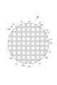
ウェハ20は、複数のライン15のそれぞれに沿って機能素子22aごとに切断される。複数のライン15は、ウェハ20の厚さ方向から見た場合に複数の機能素子22aのそれぞれの間を通っている。より具体的には、ライン15は、ウェハ20の厚さ方向から見た場合にストリート領域23の中心(幅方向における中心)を通っている。ストリート領域23は、機能素子層22において、隣り合う機能素子22aの間を通るように延在している。本実施形態では、複数の機能素子22aは、表面21aに沿ってマトリックス状に配列されており、複数のライン15は、格子状に設定されている。なお、ライン15は、仮想的なラインであるが、実際に引かれたラインであってもよい。
[レーザ照射ユニットの構成]The
[Configuration of laser irradiation unit]
図4に示されるように、レーザ照射ユニット3は、光源31と、空間光変調器32と、集光レンズ33と、を有している。光源31は、例えばパルス発振方式によって、レーザ光Lを出力する。空間光変調器32は、光源31から出力されたレーザ光Lを変調する。空間光変調器32は、例えば反射型液晶(LCOS:Liquid Crystal on Silicon)の空間光変調器(SLM:Spatial Light Modulator)である。集光レンズ33は、空間光変調器32によって変調されたレーザ光Lを集光する。 As shown in FIG. 4 , the
本実施形態では、レーザ照射ユニット3は、複数のライン15のそれぞれに沿って半導体基板21の裏面21b側からウェハ20にレーザ光Lを照射することにより、複数のライン15のそれぞれに沿って半導体基板21の内部に2列の改質領域12a,12bを形成する。改質領域(第1改質領域)12aは、2列の改質領域12a,12bのうち表面21aに最も近い改質領域である。改質領域(第2改質領域)12bは、2列の改質領域12a,12bのうち、改質領域12aに最も近い改質領域であって、裏面21bに最も近い改質領域である。 In this embodiment, the
2列の改質領域12a,12bは、ウェハ20の厚さ方向(Z方向)において隣り合っている。2列の改質領域12a,12bは、半導体基板21に対して2つの集光点C1,C2がライン15に沿って相対的に移動させられることにより形成される。レーザ光Lは、例えば集光点C1に対して集光点C2が進行方向の後側且つレーザ光Lの入射側に位置するように、空間光変調器32によって変調される。 The two rows of modified
レーザ照射ユニット3は、2列の改質領域12a,12bに渡る亀裂14が半導体基板21の表面21aに至る条件で、複数のライン15のそれぞれに沿って半導体基板21の裏面21b側からウェハ20にレーザ光Lを照射する。一例として、厚さ775μmの単結晶シリコン基板である半導体基板21に対し、表面21aから54μmの位置及び128μmの位置に2つの集光点C1,C2をそれぞれ合わせて、複数のライン15のそれぞれに沿って半導体基板21の裏面21b側からウェハ20にレーザ光Lを照射する。このとき、レーザ光Lの波長は1099nm、パルス幅は700n秒、繰り返し周波数は120kHzである。また、集光点C1におけるレーザ光Lの出力は2.7W、集光点C2におけるレーザ光Lの出力は2.7Wであり、半導体基板21に対する2つの集光点C1,C2の相対的な移動速度は800mm/秒である。 The
このような2列の改質領域12a,12b及び亀裂14の形成は、次のような場合に実施される。すなわち、後の工程において、半導体基板21の裏面21bを研削することにより半導体基板21を薄化すると共に亀裂14を裏面21bに露出させ、複数のライン15のそれぞれに沿ってウェハ20を複数の半導体デバイスに切断する場合である。
[検査用撮像ユニットの構成]Formation of such two rows of modified
[Configuration of imaging unit for inspection]
図5に示されるように、撮像ユニット4は、光源41と、ミラー42と、対物レンズ43と、光検出部44と、を有している。光源41は、半導体基板21に対して透過性を有する光I1を出力する。光源41は、例えば、ハロゲンランプ及びフィルタによって構成されており、近赤外領域の光I1を出力する。光源41から出力された光I1は、ミラー42によって反射されて対物レンズ43を通過し、半導体基板21の裏面21b側からウェハ20に照射される。このとき、ステージ2は、上述したように2列の改質領域12a,12bが形成されたウェハ20を支持している。 As shown in FIG. 5 , the
対物レンズ43は、半導体基板21の表面21aで反射された光I1を通過させる。つまり、対物レンズ43は、半導体基板21を伝搬した光I1を通過させる。対物レンズ43の開口数(NA)は、0.45以上である。対物レンズ43は、補正環43aを有している。補正環43aは、例えば対物レンズ43を構成する複数のレンズにおける相互間の距離を調整することにより、半導体基板21内において光I1に生じる収差を補正する。光検出部44は、対物レンズ43及びミラー42を透過した光I1を検出する。光検出部44は、例えば、InGaAsカメラによって構成されており、近赤外領域の光I1を検出する。 The
撮像ユニット4は、2列の改質領域12a,12bのそれぞれ、及び、複数の亀裂14a,14b,14c,14dのそれぞれの先端を撮像することができる(詳細については、後述する)。亀裂14aは、改質領域12aから表面21a側に延びる亀裂である。亀裂14bは、改質領域12aから裏面21b側に延びる亀裂である。亀裂14cは、改質領域12bから表面21a側に延びる亀裂である。亀裂14dは、改質領域12bから裏面21b側に延びる亀裂である。制御部8は、2列の改質領域12a,12bに渡る亀裂14が半導体基板21の表面21aに至る条件で、レーザ照射ユニット3にレーザ光Lを照射させるが(図4参照)、何らかの不具合等に起因して亀裂14が表面21aに至っていないと、このような複数の亀裂14a,14b,14c,14dが形成される。
[アライメント補正用撮像ユニットの構成]The
[Configuration of imaging unit for alignment correction]
図6に示されるように、撮像ユニット5は、光源51と、ミラー52と、レンズ53と、光検出部54と、を有している。光源51は、半導体基板21に対して透過性を有する光I2を出力する。光源51は、例えば、ハロゲンランプ及びフィルタによって構成されており、近赤外領域の光I2を出力する。光源51は、撮像ユニット4の光源41と共通化されていてもよい。光源51から出力された光I2は、ミラー52によって反射されてレンズ53を通過し、半導体基板21の裏面21b側からウェハ20に照射される。 As shown in FIG. 6, the
レンズ53は、半導体基板21の表面21aで反射された光I2を通過させる。つまり、レンズ53は、半導体基板21を伝搬した光I2を通過させる。レンズ53の開口数は、0.3以下である。すなわち、撮像ユニット4の対物レンズ43の開口数は、レンズ53の開口数よりも大きい。光検出部54は、レンズ53及びミラー52を通過した光I2を検出する。光検出部55は、例えば、InGaAsカメラによって構成されており、近赤外領域の光I2を検出する。 The
撮像ユニット5は、制御部8の制御のもとで、裏面21b側から光I2をウェハ20に照射すると共に、表面21a(機能素子層22)から戻る光I2を検出することにより、機能素子層22を撮像する。また、撮像ユニット5は、同様に、制御部8の制御のもとで、裏面21b側から光I2をウェハ20に照射すると共に、半導体基板21における改質領域12a,12bの形成位置から戻る光I2を検出することにより、改質領域12a,12bを含む領域の画像を取得する。これらの画像は、レーザ光Lの照射位置のアライメントに用いられる。撮像ユニット6は、レンズ53がより低倍率(例えば、撮像ユニット5においては6倍であり、撮像ユニット6においては1.5倍)である点を除いて、撮像ユニット5と同様の構成を備え、撮像ユニット5と同様にアライメントに用いられる。
[検査用撮像ユニットによる撮像原理]Under the control of the
[Imaging principle by inspection imaging unit]
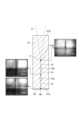
図5に示される撮像ユニット4を用い、図7に示されるように、2列の改質領域12a,12bに渡る亀裂14が表面21aに至っている半導体基板21に対して、裏面21b側から表面21a側に向かって焦点F(対物レンズ43の焦点)を移動させる。この場合、改質領域12bから裏面21b側に延びる亀裂14の先端14eに裏面21b側から焦点Fを合わせると、当該先端14eを確認することができる(図7における右側の画像)。しかし、亀裂14そのもの、及び表面21aに至っている亀裂14の先端14eに裏面21b側から焦点Fを合わせても、それらを確認することができない(図7における左側の画像)。なお、半導体基板21の表面21aに裏面21b側から焦点Fを合わせると、機能素子層22を確認することができる。 Using the
また、図5に示される撮像ユニット4を用い、図8に示されるように、2列の改質領域12a,12bに渡る亀裂14が表面21aに至っていない半導体基板21に対して、裏面21b側から表面21a側に向かって焦点Fを移動させる。この場合、改質領域12aから表面21a側に延びる亀裂14の先端14eに裏面21b側から焦点Fを合わせても、当該先端14eを確認することができない(図8における左側の画像)。しかし、表面21aに対して裏面21bとは反対側の領域(すなわち、表面21aに対して機能素子層22側の領域)に裏面21b側から焦点Fを合わせて、表面21aに関して焦点Fと対称な仮想焦点Fvを当該先端14eに位置させると、当該先端14eを確認することができる(図8における右側の画像)。なお、仮想焦点Fvは、半導体基板21の屈折率を考慮した焦点Fと表面21aに関して対称な点である。 Also, using the
以上のように亀裂14そのものを確認することができないのは、照明光である光I1の波長よりも亀裂14の幅が小さいためと想定される。図9及び図10は、シリコン基板である半導体基板21の内部に形成された改質領域12及び亀裂14のSEM(Scanning Electron Microscope)画像である。図9の(b)は、図9の(a)に示される領域A1の拡大像、図10の(a)は、図9の(b)に示される領域A2の拡大像、図10の(b)は、図10の(a)に示される領域A3の拡大像である。このように、亀裂14の幅は、120nm程度であり、近赤外領域の光I1の波長(例えば、1.1~1.2μm)よりも小さい。 The reason why the
以上を踏まえて想定される撮像原理は、次のとおりである。図11の(a)に示されるように、空気中に焦点Fを位置させると、光I1が戻ってこないため、黒っぽい画像が得られる(図11の(a)における右側の画像)。図11の(b)に示されるように、半導体基板21の内部に焦点Fを位置させると、表面21aで反射された光I1が戻ってくるため、白っぽい画像が得られる(図11の(b)における右側の画像)。図11の(c)に示されるように、改質領域12に裏面21b側から焦点Fを合わせると、改質領域12によって、表面21aで反射されて戻ってきた光I1の一部について吸収、散乱等が生じるため、白っぽい背景の中に改質領域12が黒っぽく映った画像が得られる(図11の(c)における右側の画像)。 The imaging principle assumed based on the above is as follows. As shown in FIG. 11(a), when the focal point F is positioned in the air, the light I1 does not return, resulting in a darker image (right image in FIG. 11(a)). As shown in FIG. 11(b), when the focal point F is positioned inside the
図12の(a)及び(b)に示されるように、亀裂14の先端14eに裏面21b側から焦点Fを合わせると、例えば、先端14e近傍に生じた光学的特異性(応力集中、歪、原子密度の不連続性等)、先端14e近傍で生じる光の閉じ込め等によって、表面21aで反射されて戻ってきた光I1の一部について散乱、反射、干渉、吸収等が生じるため、白っぽい背景の中に先端14eが黒っぽく映った画像が得られる(図12の(a)及び(b)における右側の画像)。図12の(c)に示されるように、亀裂14の先端14e近傍以外の部分に裏面21b側から焦点Fを合わせると、表面21aで反射された光I1の少なくとも一部が戻ってくるため、白っぽい画像が得られる(図12の(c)における右側の画像)。
[検査用撮像ユニットによる検査原理]As shown in FIGS. 12A and 12B, when the
[Inspection principle by inspection imaging unit]
制御部8が、2列の改質領域12a,12bに渡る亀裂14が半導体基板21の表面21aに至る条件で、レーザ照射ユニット3にレーザ光Lを照射させた結果、予定どおり、2列の改質領域12a,12bに渡る亀裂14が表面21aに至っている場合、亀裂14の先端14eの状態は、次のとおりとなる。すなわち、図13に示されるように、改質領域12aと表面21aとの間の領域、及び改質領域12aと改質領域12bとの間の領域には、亀裂14の先端14eが現れない。改質領域12bから裏面21b側に延びる亀裂14の先端14eの位置(以下、単に「先端位置」という)は、改質領域12bと裏面21bとの間の基準位置Pに対して裏面21b側に位置する。 As a result of the
それに対し、制御部8が、2列の改質領域12a,12bに渡る亀裂14が半導体基板21の表面21aに至る条件で、レーザ照射ユニット3にレーザ光Lを照射させた結果、予定に反して、何らかの不具合に起因して、2列の改質領域12a,12bに渡る亀裂14が表面21aに至っていない場合、亀裂14の先端14eの状態は、次のとおりとなる。すなわち、図14に示されるように、改質領域12aと表面21aとの間の領域には、改質領域12aから表面21a側に延びる亀裂14aの先端14eが現れる。改質領域12aと改質領域12bとの間の領域には、改質領域12aから裏面21b側に延びる亀裂14bの先端14e、及び改質領域12bから表面21a側に延びる亀裂14cの先端14eが現れる。改質領域12bから裏面21b側に延びる亀裂14dの先端位置は、改質領域12bと裏面21bとの間の基準位置Pに対して表面21aに位置する。 On the other hand, the
以上により、次の第1検査、第2検査、第3検査及び第4検査のうち少なくとも1つの検査を制御部8が実施すれば、2列の改質領域12a,12bに渡る亀裂14が半導体基板21の表面21aに至っているか否かを評価することができる。第1検査は、改質領域12aと表面21aとの間の領域を検査領域R1とし、検査領域R1に、改質領域12aから表面21a側に延びる亀裂14aの先端14eが存在するか否かの検査である。第2検査は、改質領域12aと改質領域12bとの間の領域を検査領域R2とし、検査領域R2に、改質領域12aから裏面21b側に延びる亀裂14bの先端14eが存在するか否かの検査である。第3検査は、検査領域R2に、改質領域12bから表面21a側に延びる亀裂14cの先端14eが存在するか否かの検査である。第4検査は、基準位置Pから裏面21b側に延び且つ裏面21bに至っていない領域を検査領域R3とし、検査領域R3に、改質領域12bから裏面21b側に延びる亀裂14dの先端位置が位置するか否かの検査である。 As described above, if the
検査領域R1、検査領域R2及び検査領域R3のそれぞれは、2列の改質領域12a,12bを形成する前に、半導体基板21に対して2つの集光点C1,C2を合わせる位置に基づいて設定可能である。2列の改質領域12a,12bに渡る亀裂14が半導体基板21の表面21aに至る場合、改質領域12bから裏面21b側に延びる亀裂14の先端位置は安定するため、基準位置P及び検査領域R3は、テスト加工の結果に基づいて設定可能である。なお、撮像ユニット4は、図13及び図14に示されるように、2つの改質領域12a,12bのそれぞれを撮像することができるため、2列の改質領域12a,12bを形成した後に、2つの改質領域12a,12bのそれぞれの位置に基づいて、検査領域R1、検査領域R2及び検査領域R3のそれぞれを設定してもよい。
[レーザ加工方法及び半導体デバイス製造方法]Each of the inspection region R1, the inspection region R2, and the inspection region R3 is based on the position where the two focal points C1 and C2 are aligned with the
[Laser processing method and semiconductor device manufacturing method]
本実施形態の半導体デバイス製造方法について、図15を参照して説明する。なお、本実施形態の半導体デバイス製造方法は、レーザ加工装置1において実施されるレーザ加工方法を含んでいる。 A semiconductor device manufacturing method according to the present embodiment will be described with reference to FIG. In addition, the semiconductor device manufacturing method of the present embodiment includes a laser processing method performed by the
まず、ウェハ20が用意され、レーザ加工装置1のステージ2に載置される。続いて、レーザ加工装置1が、複数のライン15のそれぞれに沿って半導体基板21の裏面21b側からウェハ20にレーザ光Lを照射することにより、複数のライン15のそれぞれに沿って半導体基板21の内部に2列の改質領域12a,12bを形成する(S01、第1工程)。この工程においては、レーザ加工装置1が、2列の改質領域12a,12bに渡る亀裂14が半導体基板21の表面21aに至る条件で、複数のライン15のそれぞれに沿って半導体基板21の裏面21b側からウェハ20にレーザ光Lを照射する。 First, a
続いて、レーザ加工装置1が、改質領域12bと裏面21bとの間の検査領域R3において、改質領域12bから裏面21b側に延びる亀裂14dの先端位置を検査する(S02、第2工程)。この工程においては、レーザ加工装置1が、検査領域R3内に裏面21b側から焦点Fを合わせて、表面21a側から裏面21b側に半導体基板21を伝搬する光I1を検出することにより、検査領域R3に亀裂14dの先端位置が位置するか否かを検査する。このように、本実施形態では、レーザ加工装置1が第4検査を実施する。 Subsequently, the
より具体的には、撮像ユニット4の対物レンズ43が、検査領域R3内に裏面21b側から焦点Fを合わせて、撮像ユニット4の光検出部44が、表面21a側から裏面21b側に半導体基板21を伝搬する光I1を検出する。このとき、駆動ユニット7によって撮像ユニット4がZ方向に沿って移動させられて、焦点Fが検査領域R3内をZ方向に沿って相対的に移動させられる。これにより、光検出部44が、Z方向における各箇所での画像データを取得する。そして、制御部8が、光検出部44から出力された信号(すなわち、Z方向における各箇所での画像データ)に基づいて、検査領域R3に亀裂14dの先端位置が位置するか否かを検査する。このように、本実施形態では、制御部8が検査部として機能し、ステージ2、撮像ユニット4及び制御部8が検査装置10として機能する。 More specifically, the
続いて、制御部8が、工程S02における検査結果に基づいて、工程S01における加工結果を評価する(S03、第3工程)。この工程においては、検査領域R3に亀裂14dの先端位置が位置する場合、基準位置Pに対して裏面21b側に亀裂14dの先端位置が位置することになるから、制御部8が、2列の改質領域12a,12bに渡る亀裂14が半導体基板21の表面21aに至っていると評価する。一方、検査領域R3に亀裂14dの先端位置が位置しない場合、基準位置Pに対して表面21a側に亀裂14dの先端位置が位置するとみなされ、制御部8が、2列の改質領域12a,12bに渡る亀裂14が半導体基板21の表面21aに至っていないと評価する。 Subsequently, the
続いて、2列の改質領域12a,12bに渡る亀裂14が半導体基板21の表面21aに至っていると評価された場合、制御部8が合格処理を実施する(S04)。この工程においては、制御部8が、合格処理として、レーザ加工装置1が備えるディスプレイによる合格の旨の表示、当該ディスプレイによる画像データの表示、レーザ加工装置1が備える記憶部による合格の旨の記録(ログとしての記憶)、当該記憶部による画像データの記憶等を実施させる。このように、レーザ加工装置1が備えるディスプレイは、オペレータに合格の旨を報知する報知部として機能する。 Subsequently, when it is evaluated that the
一方、2列の改質領域12a,12bに渡る亀裂14が半導体基板21の表面21aに至っていないと評価された場合、制御部8が不合格処理を実施する(S05)。この工程においては、制御部8が、不合格処理として、レーザ加工装置1が備えるランプによる不合格の旨の点灯、レーザ加工装置1が備えるディスプレイによる不合格の旨の表示、レーザ加工装置1が備える記憶部による不合格の旨の記録(ログとしての記憶)等を実施させる。このように、レーザ加工装置1が備えるランプ及びディスプレイの少なくとも1つは、オペレータに不合格の旨を報知する報知部として機能する。 On the other hand, when it is evaluated that the
以上の工程S01~工程S05が、レーザ加工装置1において実施されるレーザ加工方法である。なお、第4検査の実施タイミングは、全てのライン15のそれぞれに沿って半導体基板21の内部に2列の改質領域12a,12bを形成した後に限定されない。第4検査の実施タイミングは、一方向に延びる複数のライン15のそれぞれに沿った改質領域12a,12bの形成の後、一方向に延びる複数のライン15のそれぞれに沿った改質領域12a,12bの更なる形成の前のタイミングであって、一方向に延びるライン15に対するレーザ光Lの照射位置のアライメントが実施されるタイミングであってもよい。或いは、第4検査の実施タイミングは、一方向に延びる複数のライン15のそれぞれに沿った改質領域12a,12bの形成から、別の方向に延びる複数のライン15のそれぞれに沿った改質領域12a,12bの形成に切り替えられるタイミングであってもよい。また、第4検査の実施箇所は、格子状に設定された複数のライン15のうちの少なくとも1箇所であればよい。ただし、一方向に延びる複数のライン15のそれぞれに沿った改質領域12a,12bの形成から、別の方向に延びる複数のライン15のそれぞれに沿った改質領域12a,12bの形成に切り替えられる場合には、第4検査の実施箇所は、別の方向に延びるライン15のうちの交点(当該別の方向に延びるライン15と、一方向に延びる複数のライン15のそれぞれとの交点)を除く箇所であることが好ましい。別の方向に延びるライン15のうちの交点では、亀裂14の状態が不安定になり易いからである。 The above steps S01 to S05 are the laser processing method performed in the
工程S04の合格処理が実施された場合(すなわち、工程03において、2列の改質領域12a,12bに渡る亀裂14が半導体基板21の表面21aに至っていると評価された場合)、研削装置が、半導体基板21の裏面21bを研削することにより、2列の改質領域12a,12bに渡る亀裂14を裏面21bに露出させ、複数のライン15のそれぞれに沿ってウェハ20を複数の半導体デバイスに切断する(S06、第4工程)。 When the acceptance process of step S04 is performed (that is, when it is evaluated in step 03 that the
以上の工程S01~工程S06が、レーザ加工装置1において実施されるレーザ加工方法を含む半導体デバイス製造方法である。なお、工程S05の不合格処理が実施された場合(すなわち、工程03において、2列の改質領域12a,12bに渡る亀裂14が半導体基板21の表面21aに至っていないと評価された場合)、レーザ加工装置1の点検及び調整、ウェハ20への再度のレーザ加工(リカバリ加工)等が実施される。 The above steps S01 to S06 are the semiconductor device manufacturing method including the laser processing method performed in the
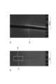
ここで、工程S06のウェハ20の研削及び切断について、より具体的に説明する。図16に示されるように、研削装置200が、半導体基板21の裏面21bを研削(研磨)することにより半導体基板21を薄化すると共に亀裂14を裏面21bに露出させ、複数のライン15のそれぞれに沿ってウェハ20を複数の半導体デバイス20aに切断する。この工程においては、研削装置200が、第4検査用の基準位置Pまで半導体基板21の裏面21bを研削する。 Here, the grinding and cutting of the
上述したように、2列の改質領域12a,12bに渡る亀裂14が半導体基板21の表面21aに至っている場合、改質領域12bから裏面21b側に延びる亀裂14の先端位置は、基準位置Pに対して裏面21b側に位置する。そのため、基準位置Pまで半導体基板21の裏面21bを研削することにより、2列の改質領域12a,12bに渡る亀裂14を裏面21bに露出させることができる。換言すれば、研削終了予定位置を基準位置Pとして、2列の改質領域12a,12bに渡る亀裂14が半導体基板21の表面21a及び基準位置Pに至る条件で、複数のライン15のそれぞれに沿って半導体基板21の裏面21b側からウェハ20にレーザ光Lを照射する。 As described above, when the
続いて、図17に示されるように、エキスパンド装置300が、半導体基板21の裏面21bに貼り付けられたエキスパンドテープ201を拡張させることにより、複数の半導体デバイス20aのそれぞれを互いに離間させる。エキスパンドテープ201は、例えば、基材201a及び接着層201bによって構成されたDAF(Die Attach Film)である。その場合、エキスパンドテープ201の拡張によって、半導体基板21の裏面21bと基材201aとの間に配置された接着層201bが半導体デバイス20aごとに切断される。切断された接着層201bは、半導体デバイス20aと共にピックアップされる。
[作用及び効果]Subsequently, as shown in FIG. 17, the expanding
[Action and effect]
上述したレーザ加工方法では、改質領域12bと半導体基板21の裏面21bとの間の検査領域R3内に裏面21b側から焦点Fを合わせて、表面21a側から裏面21b側に半導体基板21を伝搬する光I1を検出する。このように光I1を検出することにより、検査領域R3において、改質領域12bから裏面21b側に延びる亀裂14dの先端位置を確認することができる。そして、基準位置Pに対して表面21a側に亀裂14dの先端位置が位置する場合には、2列の改質領域12a,12bに渡る亀裂14が半導体基板21の表面21aに至っていないと想定される。よって、上述したレーザ加工方法によれば、2列の改質領域12a,12bに渡る亀裂14が半導体基板21の表面21aに至っているか否かを確認することができる。 In the laser processing method described above, the focus F is adjusted from the
また、上述したレーザ加工方法では、基準位置Pに対して表面21a側に亀裂14dの先端位置が位置しない場合に、2列の改質領域12a,12bに渡る亀裂14が半導体基板21の表面21aに至っていると評価し、基準位置Pに対して表面21a側に亀裂14dの先端位置が位置する場合に、2列の改質領域12a,12bに渡る亀裂14が半導体基板21の表面21aに至っていないと評価する。これにより、評価結果に基づいて、後の工程の実施態様を決定することができる。 Further, in the laser processing method described above, when the tip position of the
また、上述したレーザ加工方法では、基準位置Pから裏面21b側に延び且つ裏面21bに至っていない領域を検査領域R3とし、検査領域R3に亀裂14dの先端位置が位置する場合に、2列の改質領域12a,12bに渡る亀裂14が半導体基板21の表面21aに至っていると評価し、検査領域R3に亀裂14dの先端位置が位置しない場合に、2列の改質領域12a,12bに渡る亀裂14が半導体基板21の表面21aに至っていないと評価する。亀裂14dの先端位置は、2列の改質領域12a,12bに渡る亀裂14が半導体基板21の表面21aに至っていない場合よりも、2列の改質領域12a,12bに渡る亀裂14が半導体基板21の表面21aに至っている場合のほうが、安定する。したがって、基準位置Pから裏面21b側に延び且つ裏面21bに至っていない領域を検査領域R3とすることにより、2列の改質領域12a,12bに渡る亀裂14の検査を効率良く実施することができる。 Further, in the laser processing method described above, a region extending from the reference position P toward the
また、上述したレーザ加工方法では、複数列の改質領域12として、2列の改質領域12a,12bを形成する。これにより、複数列の改質領域12の形成、及び複数列の改質領域12に渡る亀裂14の検査を効率良く実施することができる。 Further, in the laser processing method described above, two rows of modified
また、上述した半導体デバイス製造方法によれば、2列の改質領域12a,12bに渡る亀裂14が半導体基板21の表面21aに至っていないと評価された場合に、半導体基板21の裏面21bの研削が実施されないため、研削工程の後に、ウェハ20を複数のライン15のそれぞれに沿って確実に切断することができないという事態が生じるのを防止することができる。 Further, according to the semiconductor device manufacturing method described above, when it is evaluated that the
また、上述した半導体デバイス製造方法では、基準位置Pまで半導体基板21の裏面21bを研削する。これにより、ウェハ20を複数のライン15のそれぞれに沿って確実に切断することができる。 Further, in the semiconductor device manufacturing method described above, the
また、検査装置10は、改質領域12bと半導体基板21の裏面21bとの間の検査領域R3内に裏面21b側から焦点Fを合わせて、表面21a側から裏面21b側に半導体基板21を伝搬する光I1を検出する。このように光I1を検出することにより、検査領域R3において亀裂14dの先端位置を確認することができる。 In addition, the
また、検査装置10では、対物レンズ43の開口数が0.45以上である。これにより、検査領域R3において亀裂14dの先端位置をより確実に確認することができる。 Further, in the
また、検査装置10では、対物レンズ43が補正環43aを有している。これにより、検査領域R3において亀裂14dの先端位置をより確実に確認することができる。
[変形例]Further, in the
[Modification]
本発明は、上述した実施形態に限定されない。例えば、図15に示される工程S02の検査工程において、制御部8は、上述した第4検査に加え、第1検査、第2検査及び第3検査の少なくとも1つの検査を実施してもよい。また、第4検査では、例えば改質領域12bと裏面21bとの間の全領域を検査領域R3とし、基準位置Pに対して裏面21b側に亀裂14dの先端位置が位置するか否かを検査してもよい。 The invention is not limited to the embodiments described above. For example, in the inspection process of step S02 shown in FIG. 15, the
また、上述した実施形態では、レーザ加工装置1が、複数のライン15のそれぞれに沿って半導体基板21の内部に2列の改質領域12a,12bを形成したが、レーザ加工装置1は、複数のライン15のそれぞれに沿って半導体基板21の内部に3列以上の改質領域12を形成してもよい。1本のライン15に対して形成する改質領域12の列数、位置等は、ウェハ20における半導体基板21の厚さ、半導体デバイス20aにおける半導体基板21の厚さ等を考慮して、適宜、設定可能である。なお、複数列の改質領域12は、レーザ光Lの集光点Cの相対的な移動が1本のライン15に対して複数回実施されることにより、形成されてもよい。 Further, in the above-described embodiment, the
また、図15に示される工程S06の研削及び切断工程において、研削装置200は、基準位置Pを超えて半導体基板21の裏面21bを研削してもよい。研削終了予定位置は、半導体デバイス20aの側面(切断面)に改質領域12を残すか否かに応じて、適宜、設定可能である。なお、半導体デバイス20aが例えばDRAM(Dynamic Random Access Memory)である場合には、半導体デバイス20aの側面に改質領域12が残ってもよい。 15, the grinding
また、図18に示されるように、検査装置10は、レーザ加工装置1と別体として構成されていてもよい。図18に示される検査装置10は、撮像ユニット4に加え、ステージ101と、駆動ユニット102と、制御部103と、を備えている。ステージ101は、上述したステージ2と同様に構成され、複数列の改質領域12が形成されたウェハ20を支持する。駆動ユニット102は、撮像ユニット4を支持しており、撮像ユニット4をZ方向に沿って移動させる。制御部103は、上述した制御部8と同様に構成され、検査部として機能する。図18に示されるレーザ加工システムでは、レーザ加工装置1と検査装置10との間において、ロボットハンド等の搬送装置によってウェハ20が搬送される。 Moreover, as shown in FIG. 18 , the
また、複数のライン15のそれぞれに沿って半導体基板21の裏面21b側からウェハ20にレーザ光Lを照射する際のレーザ光Lの照射条件は、上述したものに限定されない。例えば、レーザ光Lの照射条件は、上述したように、複数列の改質領域12(例えば、2列の改質領域12a,12b)に渡る亀裂14が半導体基板21と機能素子層22との界面に至る条件であってもよい。或いは、レーザ光Lの照射条件は、複数列の改質領域12に渡る亀裂14が機能素子層22における半導体基板21とは反対側の表面に至る条件であってもよい。或いは、レーザ光Lの照射条件は、複数列の改質領域12に渡る亀裂14が半導体基板21内における表面21aの近傍に至る条件であってもよい。このように、レーザ光Lの照射条件は、複数列の改質領域12に渡る亀裂14が形成される条件であればよい。いずれの場合にも、複数列の改質領域12に渡る亀裂14が半導体基板21の表面21a側に十分に延びているか否かを確認することができる。 Further, the irradiation conditions of the laser light L when the
また、上述した実施形態における各構成には、上述した材料及び形状に限定されず、様々な材料及び形状を適用することができる。また、上述した一の実施形態又は変形例における各構成は、他の実施形態又は変形例における各構成に任意に適用することができる。 In addition, various materials and shapes can be applied to each configuration in the above-described embodiments without being limited to the materials and shapes described above. Moreover, each configuration in one embodiment or modified example described above can be arbitrarily applied to each configuration in another embodiment or modified example.
2…ステージ、8…制御部(検査部)、10…検査装置、12,12a,12b…改質領域、14,14d…亀裂、14e…先端、15…ライン、20…ウェハ、20a…半導体デバイス、21…半導体基板、21a…表面、21b…裏面、22…機能素子層、22a…機能素子、41…光源、43…対物レンズ、43a…補正環、44…光検出部、F…焦点、I1…光、L…レーザ光、P…基準位置、R3…検査領域。 DESCRIPTION OF
Claims (10)
Translated fromJapanese前記複数列の改質領域のうち前記裏面に最も近い改質領域と前記裏面との間の検査領域において、前記裏面に最も近い前記改質領域から前記裏面側に延びる亀裂の先端位置を検査する第2工程と、を備え、
前記第1工程においては、前記複数列の改質領域に渡る亀裂が形成される条件で、前記複数のラインのそれぞれに沿って前記裏面側から前記ウェハに前記レーザ光を照射し、
前記第2工程においては、前記検査領域内に前記裏面側から焦点を合わせて、前記表面側から前記裏面側に前記半導体基板を伝搬する光を検出することにより、前記先端位置を検査する、レーザ加工方法。By preparing a wafer comprising a semiconductor substrate having a front surface and a back surface and a functional element layer formed on the front surface, and irradiating the wafer with laser light from the back surface side along each of a plurality of lines, a first step of forming a plurality of rows of modified regions inside the semiconductor substrate along each of the plurality of lines;
In an inspection region between the modified region closest to the back surface and the back surface among the plurality of rows of modified regions, a tip position of a crack extending from the modified region closest to the back surface to the back surface side is inspected. a second step;
In the first step, the wafer is irradiated with the laser beam from the back surface side along each of the plurality of lines under the condition that cracks are formed across the plurality of rows of modified regions;
In the second step, the tip position is inspected by focusing from the back surface side into the inspection area and detecting light propagating through the semiconductor substrate from the front surface side to the back surface side. processing method.
前記第3工程においては、前記裏面に最も近い前記改質領域と前記裏面との間の基準位置に対して前記裏面側に前記先端位置が位置する場合に、前記複数列の改質領域に渡る前記亀裂が前記表面に至っていると評価し、前記基準位置に対して前記表面側に前記先端位置が位置する場合に、前記複数列の改質領域に渡る前記亀裂が前記表面に至っていないと評価する、請求項2に記載のレーザ加工方法。Further comprising a third step of evaluating the processing result in the first step based on the inspection result in the second step,
In the third step, when the tip position is located on the back surface side with respect to a reference position between the modified region closest to the back surface and the back surface, It is evaluated that the crack reaches the surface, and when the tip position is located on the surface side with respect to the reference position, the crack extending over the multiple rows of modified regions is evaluated as not reaching the surface. The laser processing method according to claim 2, wherein
前記第3工程においては、前記検査領域に前記先端位置が位置する場合に、前記複数列の改質領域に渡る前記亀裂が前記表面に至っていると評価し、前記検査領域に前記先端位置が位置しない場合に、前記複数列の改質領域に渡る前記亀裂が前記表面に至っていないと評価する、請求項3に記載のレーザ加工方法。The inspection area is an area that extends from the reference position toward the back surface and does not reach the back surface,
In the third step, when the tip position is positioned in the inspection region, it is evaluated that the crack extending over the plurality of rows of modified regions reaches the surface, and the tip position is positioned in the inspection region. 4. The laser processing method according to claim 3, wherein the crack extending over the plurality of lines of the modified regions is evaluated as not reaching the surface if not.
前記第3工程において、前記複数列の改質領域に渡る前記亀裂が前記表面に至っていると評価された場合に、前記裏面を研削することにより、前記複数列の改質領域に渡る前記亀裂を前記裏面に露出させ、前記複数のラインのそれぞれに沿って前記ウェハを複数の半導体デバイスに切断する第4工程と、を備える、半導体デバイス製造方法。The first step, the second step and the third step included in the laser processing method according to claim 3 or 4,
In the third step, when it is evaluated that the crack extending over the multiple rows of modified regions reaches the front surface, the crack extending over the multiple rows of modified regions is removed by grinding the back surface. and a fourth step of exposing the back surface and cutting the wafer into a plurality of semiconductor devices along each of the plurality of lines.
前記半導体基板に対して透過性を有する光を出力する光源と、
前記光源から出力されて前記半導体基板を伝搬した前記光を通過させる対物レンズと、
前記対物レンズを通過した前記光を検出する光検出部と、
前記光検出部から出力された信号に基づいて、前記複数列の改質領域のうち前記裏面に最も近い改質領域と前記裏面との間の検査領域において、前記裏面に最も近い前記改質領域から前記裏面側に延びる亀裂の先端位置を検査する検査部と、を備え、
前記対物レンズは、前記検査領域内に前記裏面側から焦点を合わせ、
前記光検出部は、前記表面側から前記裏面側に前記半導体基板を伝搬する前記光を検出する、検査装置。A wafer comprising a semiconductor substrate having a front surface and a back surface, and a functional element layer formed on the front surface, wherein a plurality of rows of modified regions are formed inside the semiconductor substrate along each of a plurality of lines. a stage supporting the wafer;
a light source that outputs light having transparency to the semiconductor substrate;
an objective lens for passing the light output from the light source and propagating through the semiconductor substrate;
a photodetector that detects the light that has passed through the objective lens;
Based on the signal output from the photodetector, in an inspection region between the modified region closest to the back surface among the plurality of rows of modified regions and the back surface, the modified region closest to the back surface. and an inspection unit that inspects the tip position of the crack extending from the back surface side,
the objective lens is focused into the inspection area from the back side;
The inspection device, wherein the light detection unit detects the light propagating through the semiconductor substrate from the front surface side to the back surface side.
Priority Applications (11)
| Application Number | Priority Date | Filing Date | Title |
|---|---|---|---|
| JP2018189309AJP7307534B2 (en) | 2018-10-04 | 2018-10-04 | Laser processing method, semiconductor device manufacturing method and inspection apparatus |
| US17/281,505US12327766B2 (en) | 2018-10-04 | 2019-10-02 | Laser processing method, semiconductor device manufacturing method, and examination device |
| KR1020217011483AKR102617217B1 (en) | 2018-10-04 | 2019-10-02 | Laser processing method, semiconductor device manufacturing method and inspection device |
| DE112019004954.2TDE112019004954T5 (en) | 2018-10-04 | 2019-10-02 | Laser processing method, semiconductor device manufacturing method and test apparatus |
| PCT/JP2019/039002WO2020071455A1 (en) | 2018-10-04 | 2019-10-02 | Laser processing method, semiconductor device manufacturing method, and examination device |
| CN202411858749.XACN119747843A (en) | 2018-10-04 | 2019-10-02 | Laser processing method, semiconductor device manufacturing method and inspection device |
| CN201980065075.9ACN112789707B (en) | 2018-10-04 | 2019-10-02 | Laser processing method, semiconductor device manufacturing method and inspection device |
| KR1020237043874AKR102658812B1 (en) | 2018-10-04 | 2019-10-02 | Laser processing method, semiconductor device manufacturing method, and examination device |
| TW108135823ATWI848983B (en) | 2018-10-04 | 2019-10-03 | Laser processing method, semiconductor device manufacturing method and inspection device |
| JP2023108163AJP7554318B2 (en) | 2018-10-04 | 2023-06-30 | Laser processing method, semiconductor device manufacturing method and inspection apparatus |
| US19/192,897US20250309000A1 (en) | 2018-10-04 | 2025-04-29 | Laser processing method, semiconductor device manufacturing method, and examination device |
Applications Claiming Priority (1)
| Application Number | Priority Date | Filing Date | Title |
|---|---|---|---|
| JP2018189309AJP7307534B2 (en) | 2018-10-04 | 2018-10-04 | Laser processing method, semiconductor device manufacturing method and inspection apparatus |
Related Child Applications (1)
| Application Number | Title | Priority Date | Filing Date |
|---|---|---|---|
| JP2023108163ADivisionJP7554318B2 (en) | 2018-10-04 | 2023-06-30 | Laser processing method, semiconductor device manufacturing method and inspection apparatus |
Publications (2)
| Publication Number | Publication Date |
|---|---|
| JP2020057743A JP2020057743A (en) | 2020-04-09 |
| JP7307534B2true JP7307534B2 (en) | 2023-07-12 |
Family
ID=70055806
Family Applications (2)
| Application Number | Title | Priority Date | Filing Date |
|---|---|---|---|
| JP2018189309AActiveJP7307534B2 (en) | 2018-10-04 | 2018-10-04 | Laser processing method, semiconductor device manufacturing method and inspection apparatus |
| JP2023108163AActiveJP7554318B2 (en) | 2018-10-04 | 2023-06-30 | Laser processing method, semiconductor device manufacturing method and inspection apparatus |
Family Applications After (1)
| Application Number | Title | Priority Date | Filing Date |
|---|---|---|---|
| JP2023108163AActiveJP7554318B2 (en) | 2018-10-04 | 2023-06-30 | Laser processing method, semiconductor device manufacturing method and inspection apparatus |
Country Status (7)
| Country | Link |
|---|---|
| US (2) | US12327766B2 (en) |
| JP (2) | JP7307534B2 (en) |
| KR (2) | KR102617217B1 (en) |
| CN (2) | CN119747843A (en) |
| DE (1) | DE112019004954T5 (en) |
| TW (1) | TWI848983B (en) |
| WO (1) | WO2020071455A1 (en) |
Families Citing this family (10)
| Publication number | Priority date | Publication date | Assignee | Title |
|---|---|---|---|---|
| JP7582788B2 (en)* | 2020-04-06 | 2024-11-13 | 浜松ホトニクス株式会社 | Laser processing device and laser processing method |
| JP7455476B2 (en)* | 2020-05-28 | 2024-03-26 | 株式会社ディスコ | Wafer inspection equipment and wafer inspection method |
| JP7529478B2 (en)* | 2020-08-13 | 2024-08-06 | 株式会社ディスコ | Wafer Processing Method |
| JP7663800B2 (en)* | 2020-12-02 | 2025-04-17 | 株式会社東京精密 | Crack detection device and laser processing system |
| JP7625426B2 (en)* | 2021-01-28 | 2025-02-03 | 浜松ホトニクス株式会社 | Observation device and observation method |
| JP7665345B2 (en)* | 2021-01-29 | 2025-04-21 | 浜松ホトニクス株式会社 | Observation device and observation method |
| JP2022117064A (en)* | 2021-01-29 | 2022-08-10 | 浜松ホトニクス株式会社 | Observation device, observation method, and observation object |
| JP7720163B2 (en) | 2021-04-30 | 2025-08-07 | 株式会社キーエンス | Analyzer |
| JP7717487B2 (en)* | 2021-04-30 | 2025-08-04 | 株式会社キーエンス | Analyzer |
| JP7682780B2 (en)* | 2021-12-09 | 2025-05-26 | 浜松ホトニクス株式会社 | Laser Processing Equipment |
Citations (5)
| Publication number | Priority date | Publication date | Assignee | Title |
|---|---|---|---|---|
| JP2007132761A (en) | 2005-11-09 | 2007-05-31 | Showa Seiki Kk | Confocal signal light detection apparatus and signal light detection method |
| JP2008147818A (en) | 2006-12-07 | 2008-06-26 | Sony Corp | Solid-state imaging device, driving method of solid-state imaging device, and imaging device |
| JP2017064746A (en) | 2015-09-29 | 2017-04-06 | 株式会社東京精密 | Laser processing apparatus and laser processing method |
| JP2017133997A (en) | 2016-01-29 | 2017-08-03 | 株式会社東京精密 | Device and method for detecting cracks |
| JP2018098296A (en) | 2016-12-09 | 2018-06-21 | 株式会社ディスコ | Wafer processing method |
Family Cites Families (16)
| Publication number | Priority date | Publication date | Assignee | Title |
|---|---|---|---|---|
| US6407360B1 (en)* | 1998-08-26 | 2002-06-18 | Samsung Electronics, Co., Ltd. | Laser cutting apparatus and method |
| EP1742253B1 (en)* | 2004-03-30 | 2012-05-09 | Hamamatsu Photonics K.K. | Laser processing method |
| KR101109860B1 (en)* | 2004-08-06 | 2012-02-21 | 하마마츠 포토닉스 가부시키가이샤 | Laser processing method, cutting method for work and semiconductor device |
| JP2006147818A (en) | 2004-11-19 | 2006-06-08 | Canon Inc | Substrate cutting method |
| JP5449665B2 (en)* | 2007-10-30 | 2014-03-19 | 浜松ホトニクス株式会社 | Laser processing method |
| KR101757937B1 (en)* | 2009-02-09 | 2017-07-13 | 하마마츠 포토닉스 가부시키가이샤 | Workpiece cutting method |
| JP5639997B2 (en)* | 2009-04-07 | 2014-12-10 | 浜松ホトニクス株式会社 | Laser processing equipment |
| JP5491761B2 (en) | 2009-04-20 | 2014-05-14 | 浜松ホトニクス株式会社 | Laser processing equipment |
| JP5707889B2 (en) | 2010-11-16 | 2015-04-30 | 株式会社東京精密 | Semiconductor substrate cutting method and semiconductor substrate cutting apparatus |
| JP5985896B2 (en) | 2012-06-12 | 2016-09-06 | 株式会社ディスコ | Wafer processing method and laser processing apparatus |
| KR101683706B1 (en)* | 2012-09-28 | 2016-12-07 | 제이엑스 에네루기 가부시키가이샤 | Device for inspecting substrate having irregular rough surface and inspection method using same |
| JP6121733B2 (en)* | 2013-01-31 | 2017-04-26 | 浜松ホトニクス株式会社 | Laser processing apparatus and laser processing method |
| JP6353683B2 (en) | 2014-04-04 | 2018-07-04 | 浜松ホトニクス株式会社 | Laser processing apparatus and laser processing method |
| TW201628751A (en)* | 2014-11-20 | 2016-08-16 | 康寧公司 | Feedback-controlled laser cutting of flexible glass substrates |
| JP6560040B2 (en) | 2015-07-06 | 2019-08-14 | 株式会社ディスコ | Wafer processing method |
| JP7171353B2 (en)* | 2018-10-04 | 2022-11-15 | 浜松ホトニクス株式会社 | Laser processing method, semiconductor device manufacturing method and inspection device |
- 2018
- 2018-10-04JPJP2018189309Apatent/JP7307534B2/enactiveActive
- 2019
- 2019-10-02USUS17/281,505patent/US12327766B2/enactiveActive
- 2019-10-02WOPCT/JP2019/039002patent/WO2020071455A1/ennot_activeCeased
- 2019-10-02CNCN202411858749.XApatent/CN119747843A/enactivePending
- 2019-10-02DEDE112019004954.2Tpatent/DE112019004954T5/enactivePending
- 2019-10-02KRKR1020217011483Apatent/KR102617217B1/enactiveActive
- 2019-10-02KRKR1020237043874Apatent/KR102658812B1/enactiveActive
- 2019-10-02CNCN201980065075.9Apatent/CN112789707B/enactiveActive
- 2019-10-03TWTW108135823Apatent/TWI848983B/enactive
- 2023
- 2023-06-30JPJP2023108163Apatent/JP7554318B2/enactiveActive
- 2025
- 2025-04-29USUS19/192,897patent/US20250309000A1/enactivePending
Patent Citations (5)
| Publication number | Priority date | Publication date | Assignee | Title |
|---|---|---|---|---|
| JP2007132761A (en) | 2005-11-09 | 2007-05-31 | Showa Seiki Kk | Confocal signal light detection apparatus and signal light detection method |
| JP2008147818A (en) | 2006-12-07 | 2008-06-26 | Sony Corp | Solid-state imaging device, driving method of solid-state imaging device, and imaging device |
| JP2017064746A (en) | 2015-09-29 | 2017-04-06 | 株式会社東京精密 | Laser processing apparatus and laser processing method |
| JP2017133997A (en) | 2016-01-29 | 2017-08-03 | 株式会社東京精密 | Device and method for detecting cracks |
| JP2018098296A (en) | 2016-12-09 | 2018-06-21 | 株式会社ディスコ | Wafer processing method |
Also Published As
| Publication number | Publication date |
|---|---|
| DE112019004954T5 (en) | 2021-06-17 |
| CN119747843A (en) | 2025-04-04 |
| JP7554318B2 (en) | 2024-09-19 |
| CN112789707B (en) | 2025-01-03 |
| TW202027897A (en) | 2020-08-01 |
| US20250309000A1 (en) | 2025-10-02 |
| KR102617217B1 (en) | 2023-12-27 |
| WO2020071455A1 (en) | 2020-04-09 |
| KR102658812B1 (en) | 2024-04-19 |
| JP2020057743A (en) | 2020-04-09 |
| JP2023129439A (en) | 2023-09-14 |
| CN112789707A (en) | 2021-05-11 |
| US12327766B2 (en) | 2025-06-10 |
| US20210398855A1 (en) | 2021-12-23 |
| TWI848983B (en) | 2024-07-21 |
| KR20230175348A (en) | 2023-12-29 |
| KR20210069657A (en) | 2021-06-11 |
Similar Documents
| Publication | Publication Date | Title |
|---|---|---|
| JP7307534B2 (en) | Laser processing method, semiconductor device manufacturing method and inspection apparatus | |
| JP7313128B2 (en) | IMAGING DEVICE, LASER PROCESSING DEVICE, AND IMAGING METHOD | |
| JP7313127B2 (en) | IMAGING DEVICE, LASER PROCESSING DEVICE, AND IMAGING METHOD | |
| JP7171353B2 (en) | Laser processing method, semiconductor device manufacturing method and inspection device | |
| JP7307533B2 (en) | Laser processing method, semiconductor device manufacturing method and inspection device | |
| JP7319770B2 (en) | IMAGING DEVICE, LASER PROCESSING DEVICE, AND IMAGING METHOD |
Legal Events
| Date | Code | Title | Description |
|---|---|---|---|
| A621 | Written request for application examination | Free format text:JAPANESE INTERMEDIATE CODE: A621 Effective date:20210930 | |
| A131 | Notification of reasons for refusal | Free format text:JAPANESE INTERMEDIATE CODE: A131 Effective date:20221101 | |
| A601 | Written request for extension of time | Free format text:JAPANESE INTERMEDIATE CODE: A601 Effective date:20221222 | |
| TRDD | Decision of grant or rejection written | ||
| A01 | Written decision to grant a patent or to grant a registration (utility model) | Free format text:JAPANESE INTERMEDIATE CODE: A01 Effective date:20230509 | |
| A601 | Written request for extension of time | Free format text:JAPANESE INTERMEDIATE CODE: A601 Effective date:20230607 | |
| A61 | First payment of annual fees (during grant procedure) | Free format text:JAPANESE INTERMEDIATE CODE: A61 Effective date:20230630 | |
| R150 | Certificate of patent or registration of utility model | Ref document number:7307534 Country of ref document:JP Free format text:JAPANESE INTERMEDIATE CODE: R150 |