JP7301805B2 - semiconductor module - Google Patents
semiconductor moduleDownload PDFInfo
- Publication number
- JP7301805B2 JP7301805B2JP2020160230AJP2020160230AJP7301805B2JP 7301805 B2JP7301805 B2JP 7301805B2JP 2020160230 AJP2020160230 AJP 2020160230AJP 2020160230 AJP2020160230 AJP 2020160230AJP 7301805 B2JP7301805 B2JP 7301805B2
- Authority
- JP
- Japan
- Prior art keywords
- semiconductor device
- wiring layer
- semiconductor
- electrode
- semiconductor module
- Prior art date
- Legal status (The legal status is an assumption and is not a legal conclusion. Google has not performed a legal analysis and makes no representation as to the accuracy of the status listed.)
- Active
Links
Images
Classifications
- H—ELECTRICITY
- H01—ELECTRIC ELEMENTS
- H01L—SEMICONDUCTOR DEVICES NOT COVERED BY CLASS H10
- H01L23/00—Details of semiconductor or other solid state devices
- H01L23/52—Arrangements for conducting electric current within the device in operation from one component to another, i.e. interconnections, e.g. wires, lead frames
- H01L23/538—Arrangements for conducting electric current within the device in operation from one component to another, i.e. interconnections, e.g. wires, lead frames the interconnection structure between a plurality of semiconductor chips being formed on, or in, insulating substrates
- H01L23/5385—Assembly of a plurality of insulating substrates
- H—ELECTRICITY
- H01—ELECTRIC ELEMENTS
- H01L—SEMICONDUCTOR DEVICES NOT COVERED BY CLASS H10
- H01L24/00—Arrangements for connecting or disconnecting semiconductor or solid-state bodies; Methods or apparatus related thereto
- H01L24/01—Means for bonding being attached to, or being formed on, the surface to be connected, e.g. chip-to-package, die-attach, "first-level" interconnects; Manufacturing methods related thereto
- H01L24/34—Strap connectors, e.g. copper straps for grounding power devices; Manufacturing methods related thereto
- H01L24/39—Structure, shape, material or disposition of the strap connectors after the connecting process
- H01L24/40—Structure, shape, material or disposition of the strap connectors after the connecting process of an individual strap connector
- H—ELECTRICITY
- H01—ELECTRIC ELEMENTS
- H01L—SEMICONDUCTOR DEVICES NOT COVERED BY CLASS H10
- H01L23/00—Details of semiconductor or other solid state devices
- H01L23/34—Arrangements for cooling, heating, ventilating or temperature compensation ; Temperature sensing arrangements
- H01L23/40—Mountings or securing means for detachable cooling or heating arrangements ; fixed by friction, plugs or springs
- H—ELECTRICITY
- H01—ELECTRIC ELEMENTS
- H01L—SEMICONDUCTOR DEVICES NOT COVERED BY CLASS H10
- H01L23/00—Details of semiconductor or other solid state devices
- H01L23/34—Arrangements for cooling, heating, ventilating or temperature compensation ; Temperature sensing arrangements
- H01L23/42—Fillings or auxiliary members in containers or encapsulations selected or arranged to facilitate heating or cooling
- H01L23/433—Auxiliary members in containers characterised by their shape, e.g. pistons
- H01L23/4334—Auxiliary members in encapsulations
- H—ELECTRICITY
- H01—ELECTRIC ELEMENTS
- H01L—SEMICONDUCTOR DEVICES NOT COVERED BY CLASS H10
- H01L23/00—Details of semiconductor or other solid state devices
- H01L23/48—Arrangements for conducting electric current to or from the solid state body in operation, e.g. leads, terminal arrangements ; Selection of materials therefor
- H01L23/488—Arrangements for conducting electric current to or from the solid state body in operation, e.g. leads, terminal arrangements ; Selection of materials therefor consisting of soldered or bonded constructions
- H01L23/498—Leads, i.e. metallisations or lead-frames on insulating substrates, e.g. chip carriers
- H01L23/49811—Additional leads joined to the metallisation on the insulating substrate, e.g. pins, bumps, wires, flat leads
- H—ELECTRICITY
- H01—ELECTRIC ELEMENTS
- H01L—SEMICONDUCTOR DEVICES NOT COVERED BY CLASS H10
- H01L23/00—Details of semiconductor or other solid state devices
- H01L23/48—Arrangements for conducting electric current to or from the solid state body in operation, e.g. leads, terminal arrangements ; Selection of materials therefor
- H01L23/488—Arrangements for conducting electric current to or from the solid state body in operation, e.g. leads, terminal arrangements ; Selection of materials therefor consisting of soldered or bonded constructions
- H01L23/498—Leads, i.e. metallisations or lead-frames on insulating substrates, e.g. chip carriers
- H01L23/49838—Geometry or layout
- H—ELECTRICITY
- H01—ELECTRIC ELEMENTS
- H01L—SEMICONDUCTOR DEVICES NOT COVERED BY CLASS H10
- H01L24/00—Arrangements for connecting or disconnecting semiconductor or solid-state bodies; Methods or apparatus related thereto
- H01L24/01—Means for bonding being attached to, or being formed on, the surface to be connected, e.g. chip-to-package, die-attach, "first-level" interconnects; Manufacturing methods related thereto
- H01L24/26—Layer connectors, e.g. plate connectors, solder or adhesive layers; Manufacturing methods related thereto
- H01L24/28—Structure, shape, material or disposition of the layer connectors prior to the connecting process
- H01L24/29—Structure, shape, material or disposition of the layer connectors prior to the connecting process of an individual layer connector
- H—ELECTRICITY
- H01—ELECTRIC ELEMENTS
- H01L—SEMICONDUCTOR DEVICES NOT COVERED BY CLASS H10
- H01L24/00—Arrangements for connecting or disconnecting semiconductor or solid-state bodies; Methods or apparatus related thereto
- H01L24/01—Means for bonding being attached to, or being formed on, the surface to be connected, e.g. chip-to-package, die-attach, "first-level" interconnects; Manufacturing methods related thereto
- H01L24/26—Layer connectors, e.g. plate connectors, solder or adhesive layers; Manufacturing methods related thereto
- H01L24/31—Structure, shape, material or disposition of the layer connectors after the connecting process
- H01L24/32—Structure, shape, material or disposition of the layer connectors after the connecting process of an individual layer connector
- H—ELECTRICITY
- H01—ELECTRIC ELEMENTS
- H01L—SEMICONDUCTOR DEVICES NOT COVERED BY CLASS H10
- H01L24/00—Arrangements for connecting or disconnecting semiconductor or solid-state bodies; Methods or apparatus related thereto
- H01L24/01—Means for bonding being attached to, or being formed on, the surface to be connected, e.g. chip-to-package, die-attach, "first-level" interconnects; Manufacturing methods related thereto
- H01L24/34—Strap connectors, e.g. copper straps for grounding power devices; Manufacturing methods related thereto
- H01L24/36—Structure, shape, material or disposition of the strap connectors prior to the connecting process
- H01L24/37—Structure, shape, material or disposition of the strap connectors prior to the connecting process of an individual strap connector
- H—ELECTRICITY
- H01—ELECTRIC ELEMENTS
- H01L—SEMICONDUCTOR DEVICES NOT COVERED BY CLASS H10
- H01L24/00—Arrangements for connecting or disconnecting semiconductor or solid-state bodies; Methods or apparatus related thereto
- H01L24/01—Means for bonding being attached to, or being formed on, the surface to be connected, e.g. chip-to-package, die-attach, "first-level" interconnects; Manufacturing methods related thereto
- H01L24/34—Strap connectors, e.g. copper straps for grounding power devices; Manufacturing methods related thereto
- H01L24/39—Structure, shape, material or disposition of the strap connectors after the connecting process
- H01L24/41—Structure, shape, material or disposition of the strap connectors after the connecting process of a plurality of strap connectors
- H—ELECTRICITY
- H01—ELECTRIC ELEMENTS
- H01L—SEMICONDUCTOR DEVICES NOT COVERED BY CLASS H10
- H01L24/00—Arrangements for connecting or disconnecting semiconductor or solid-state bodies; Methods or apparatus related thereto
- H01L24/73—Means for bonding being of different types provided for in two or more of groups H01L24/10, H01L24/18, H01L24/26, H01L24/34, H01L24/42, H01L24/50, H01L24/63, H01L24/71
- H—ELECTRICITY
- H01—ELECTRIC ELEMENTS
- H01L—SEMICONDUCTOR DEVICES NOT COVERED BY CLASS H10
- H01L25/00—Assemblies consisting of a plurality of semiconductor or other solid state devices
- H01L25/03—Assemblies consisting of a plurality of semiconductor or other solid state devices all the devices being of a type provided for in a single subclass of subclasses H10B, H10D, H10F, H10H, H10K or H10N, e.g. assemblies of rectifier diodes
- H01L25/04—Assemblies consisting of a plurality of semiconductor or other solid state devices all the devices being of a type provided for in a single subclass of subclasses H10B, H10D, H10F, H10H, H10K or H10N, e.g. assemblies of rectifier diodes the devices not having separate containers
- H01L25/065—Assemblies consisting of a plurality of semiconductor or other solid state devices all the devices being of a type provided for in a single subclass of subclasses H10B, H10D, H10F, H10H, H10K or H10N, e.g. assemblies of rectifier diodes the devices not having separate containers the devices being of a type provided for in group H10D89/00
- H01L25/0655—Assemblies consisting of a plurality of semiconductor or other solid state devices all the devices being of a type provided for in a single subclass of subclasses H10B, H10D, H10F, H10H, H10K or H10N, e.g. assemblies of rectifier diodes the devices not having separate containers the devices being of a type provided for in group H10D89/00 the devices being arranged next to each other
- H—ELECTRICITY
- H01—ELECTRIC ELEMENTS
- H01L—SEMICONDUCTOR DEVICES NOT COVERED BY CLASS H10
- H01L25/00—Assemblies consisting of a plurality of semiconductor or other solid state devices
- H01L25/03—Assemblies consisting of a plurality of semiconductor or other solid state devices all the devices being of a type provided for in a single subclass of subclasses H10B, H10D, H10F, H10H, H10K or H10N, e.g. assemblies of rectifier diodes
- H01L25/04—Assemblies consisting of a plurality of semiconductor or other solid state devices all the devices being of a type provided for in a single subclass of subclasses H10B, H10D, H10F, H10H, H10K or H10N, e.g. assemblies of rectifier diodes the devices not having separate containers
- H01L25/07—Assemblies consisting of a plurality of semiconductor or other solid state devices all the devices being of a type provided for in a single subclass of subclasses H10B, H10D, H10F, H10H, H10K or H10N, e.g. assemblies of rectifier diodes the devices not having separate containers the devices being of a type provided for in group subclass H10D
- H01L25/072—Assemblies consisting of a plurality of semiconductor or other solid state devices all the devices being of a type provided for in a single subclass of subclasses H10B, H10D, H10F, H10H, H10K or H10N, e.g. assemblies of rectifier diodes the devices not having separate containers the devices being of a type provided for in group subclass H10D the devices being arranged next to each other
- H—ELECTRICITY
- H01—ELECTRIC ELEMENTS
- H01L—SEMICONDUCTOR DEVICES NOT COVERED BY CLASS H10
- H01L2224/00—Indexing scheme for arrangements for connecting or disconnecting semiconductor or solid-state bodies and methods related thereto as covered by H01L24/00
- H01L2224/01—Means for bonding being attached to, or being formed on, the surface to be connected, e.g. chip-to-package, die-attach, "first-level" interconnects; Manufacturing methods related thereto
- H01L2224/26—Layer connectors, e.g. plate connectors, solder or adhesive layers; Manufacturing methods related thereto
- H01L2224/28—Structure, shape, material or disposition of the layer connectors prior to the connecting process
- H01L2224/29—Structure, shape, material or disposition of the layer connectors prior to the connecting process of an individual layer connector
- H01L2224/29001—Core members of the layer connector
- H01L2224/29099—Material
- H01L2224/29198—Material with a principal constituent of the material being a combination of two or more materials in the form of a matrix with a filler, i.e. being a hybrid material, e.g. segmented structures, foams
- H01L2224/29298—Fillers
- H01L2224/29299—Base material
- H—ELECTRICITY
- H01—ELECTRIC ELEMENTS
- H01L—SEMICONDUCTOR DEVICES NOT COVERED BY CLASS H10
- H01L2224/00—Indexing scheme for arrangements for connecting or disconnecting semiconductor or solid-state bodies and methods related thereto as covered by H01L24/00
- H01L2224/01—Means for bonding being attached to, or being formed on, the surface to be connected, e.g. chip-to-package, die-attach, "first-level" interconnects; Manufacturing methods related thereto
- H01L2224/26—Layer connectors, e.g. plate connectors, solder or adhesive layers; Manufacturing methods related thereto
- H01L2224/31—Structure, shape, material or disposition of the layer connectors after the connecting process
- H01L2224/32—Structure, shape, material or disposition of the layer connectors after the connecting process of an individual layer connector
- H01L2224/321—Disposition
- H01L2224/32151—Disposition the layer connector connecting between a semiconductor or solid-state body and an item not being a semiconductor or solid-state body, e.g. chip-to-substrate, chip-to-passive
- H01L2224/32221—Disposition the layer connector connecting between a semiconductor or solid-state body and an item not being a semiconductor or solid-state body, e.g. chip-to-substrate, chip-to-passive the body and the item being stacked
- H01L2224/32225—Disposition the layer connector connecting between a semiconductor or solid-state body and an item not being a semiconductor or solid-state body, e.g. chip-to-substrate, chip-to-passive the body and the item being stacked the item being non-metallic, e.g. insulating substrate with or without metallisation
- H01L2224/32227—Disposition the layer connector connecting between a semiconductor or solid-state body and an item not being a semiconductor or solid-state body, e.g. chip-to-substrate, chip-to-passive the body and the item being stacked the item being non-metallic, e.g. insulating substrate with or without metallisation the layer connector connecting to a bond pad of the item
- H—ELECTRICITY
- H01—ELECTRIC ELEMENTS
- H01L—SEMICONDUCTOR DEVICES NOT COVERED BY CLASS H10
- H01L2224/00—Indexing scheme for arrangements for connecting or disconnecting semiconductor or solid-state bodies and methods related thereto as covered by H01L24/00
- H01L2224/01—Means for bonding being attached to, or being formed on, the surface to be connected, e.g. chip-to-package, die-attach, "first-level" interconnects; Manufacturing methods related thereto
- H01L2224/26—Layer connectors, e.g. plate connectors, solder or adhesive layers; Manufacturing methods related thereto
- H01L2224/31—Structure, shape, material or disposition of the layer connectors after the connecting process
- H01L2224/32—Structure, shape, material or disposition of the layer connectors after the connecting process of an individual layer connector
- H01L2224/321—Disposition
- H01L2224/32151—Disposition the layer connector connecting between a semiconductor or solid-state body and an item not being a semiconductor or solid-state body, e.g. chip-to-substrate, chip-to-passive
- H01L2224/32221—Disposition the layer connector connecting between a semiconductor or solid-state body and an item not being a semiconductor or solid-state body, e.g. chip-to-substrate, chip-to-passive the body and the item being stacked
- H01L2224/32225—Disposition the layer connector connecting between a semiconductor or solid-state body and an item not being a semiconductor or solid-state body, e.g. chip-to-substrate, chip-to-passive the body and the item being stacked the item being non-metallic, e.g. insulating substrate with or without metallisation
- H01L2224/32238—Disposition the layer connector connecting between a semiconductor or solid-state body and an item not being a semiconductor or solid-state body, e.g. chip-to-substrate, chip-to-passive the body and the item being stacked the item being non-metallic, e.g. insulating substrate with or without metallisation the layer connector connecting to a bonding area protruding from the surface of the item
- H—ELECTRICITY
- H01—ELECTRIC ELEMENTS
- H01L—SEMICONDUCTOR DEVICES NOT COVERED BY CLASS H10
- H01L2224/00—Indexing scheme for arrangements for connecting or disconnecting semiconductor or solid-state bodies and methods related thereto as covered by H01L24/00
- H01L2224/01—Means for bonding being attached to, or being formed on, the surface to be connected, e.g. chip-to-package, die-attach, "first-level" interconnects; Manufacturing methods related thereto
- H01L2224/34—Strap connectors, e.g. copper straps for grounding power devices; Manufacturing methods related thereto
- H01L2224/36—Structure, shape, material or disposition of the strap connectors prior to the connecting process
- H01L2224/37—Structure, shape, material or disposition of the strap connectors prior to the connecting process of an individual strap connector
- H01L2224/37001—Core members of the connector
- H01L2224/3701—Shape
- H01L2224/37012—Cross-sectional shape
- H01L2224/37013—Cross-sectional shape being non uniform along the connector
- H—ELECTRICITY
- H01—ELECTRIC ELEMENTS
- H01L—SEMICONDUCTOR DEVICES NOT COVERED BY CLASS H10
- H01L2224/00—Indexing scheme for arrangements for connecting or disconnecting semiconductor or solid-state bodies and methods related thereto as covered by H01L24/00
- H01L2224/01—Means for bonding being attached to, or being formed on, the surface to be connected, e.g. chip-to-package, die-attach, "first-level" interconnects; Manufacturing methods related thereto
- H01L2224/34—Strap connectors, e.g. copper straps for grounding power devices; Manufacturing methods related thereto
- H01L2224/39—Structure, shape, material or disposition of the strap connectors after the connecting process
- H01L2224/40—Structure, shape, material or disposition of the strap connectors after the connecting process of an individual strap connector
- H01L2224/401—Disposition
- H01L2224/40135—Connecting between different semiconductor or solid-state bodies, i.e. chip-to-chip
- H01L2224/40137—Connecting between different semiconductor or solid-state bodies, i.e. chip-to-chip the bodies being arranged next to each other, e.g. on a common substrate
- H—ELECTRICITY
- H01—ELECTRIC ELEMENTS
- H01L—SEMICONDUCTOR DEVICES NOT COVERED BY CLASS H10
- H01L2224/00—Indexing scheme for arrangements for connecting or disconnecting semiconductor or solid-state bodies and methods related thereto as covered by H01L24/00
- H01L2224/01—Means for bonding being attached to, or being formed on, the surface to be connected, e.g. chip-to-package, die-attach, "first-level" interconnects; Manufacturing methods related thereto
- H01L2224/34—Strap connectors, e.g. copper straps for grounding power devices; Manufacturing methods related thereto
- H01L2224/39—Structure, shape, material or disposition of the strap connectors after the connecting process
- H01L2224/40—Structure, shape, material or disposition of the strap connectors after the connecting process of an individual strap connector
- H01L2224/401—Disposition
- H01L2224/40151—Connecting between a semiconductor or solid-state body and an item not being a semiconductor or solid-state body, e.g. chip-to-substrate, chip-to-passive
- H01L2224/40221—Connecting between a semiconductor or solid-state body and an item not being a semiconductor or solid-state body, e.g. chip-to-substrate, chip-to-passive the body and the item being stacked
- H01L2224/40225—Connecting between a semiconductor or solid-state body and an item not being a semiconductor or solid-state body, e.g. chip-to-substrate, chip-to-passive the body and the item being stacked the item being non-metallic, e.g. insulating substrate with or without metallisation
- H01L2224/40227—Connecting the strap to a bond pad of the item
- H—ELECTRICITY
- H01—ELECTRIC ELEMENTS
- H01L—SEMICONDUCTOR DEVICES NOT COVERED BY CLASS H10
- H01L23/00—Details of semiconductor or other solid state devices
- H01L23/34—Arrangements for cooling, heating, ventilating or temperature compensation ; Temperature sensing arrangements
- H01L23/36—Selection of materials, or shaping, to facilitate cooling or heating, e.g. heatsinks
- H01L23/373—Cooling facilitated by selection of materials for the device or materials for thermal expansion adaptation, e.g. carbon
- H01L23/3735—Laminates or multilayers, e.g. direct bond copper ceramic substrates
- H—ELECTRICITY
- H01—ELECTRIC ELEMENTS
- H01L—SEMICONDUCTOR DEVICES NOT COVERED BY CLASS H10
- H01L24/00—Arrangements for connecting or disconnecting semiconductor or solid-state bodies; Methods or apparatus related thereto
- H01L24/01—Means for bonding being attached to, or being formed on, the surface to be connected, e.g. chip-to-package, die-attach, "first-level" interconnects; Manufacturing methods related thereto
- H01L24/26—Layer connectors, e.g. plate connectors, solder or adhesive layers; Manufacturing methods related thereto
- H01L24/28—Structure, shape, material or disposition of the layer connectors prior to the connecting process
- H01L24/30—Structure, shape, material or disposition of the layer connectors prior to the connecting process of a plurality of layer connectors
- H—ELECTRICITY
- H01—ELECTRIC ELEMENTS
- H01L—SEMICONDUCTOR DEVICES NOT COVERED BY CLASS H10
- H01L24/00—Arrangements for connecting or disconnecting semiconductor or solid-state bodies; Methods or apparatus related thereto
- H01L24/01—Means for bonding being attached to, or being formed on, the surface to be connected, e.g. chip-to-package, die-attach, "first-level" interconnects; Manufacturing methods related thereto
- H01L24/34—Strap connectors, e.g. copper straps for grounding power devices; Manufacturing methods related thereto
- H01L24/36—Structure, shape, material or disposition of the strap connectors prior to the connecting process
- H01L24/38—Structure, shape, material or disposition of the strap connectors prior to the connecting process of a plurality of strap connectors
- H—ELECTRICITY
- H01—ELECTRIC ELEMENTS
- H01L—SEMICONDUCTOR DEVICES NOT COVERED BY CLASS H10
- H01L24/00—Arrangements for connecting or disconnecting semiconductor or solid-state bodies; Methods or apparatus related thereto
- H01L24/80—Methods for connecting semiconductor or other solid state bodies using means for bonding being attached to, or being formed on, the surface to be connected
- H01L24/83—Methods for connecting semiconductor or other solid state bodies using means for bonding being attached to, or being formed on, the surface to be connected using a layer connector
Landscapes
- Engineering & Computer Science (AREA)
- Microelectronics & Electronic Packaging (AREA)
- Power Engineering (AREA)
- Computer Hardware Design (AREA)
- Physics & Mathematics (AREA)
- Condensed Matter Physics & Semiconductors (AREA)
- General Physics & Mathematics (AREA)
- Geometry (AREA)
- Cooling Or The Like Of Semiconductors Or Solid State Devices (AREA)
Description
Translated fromJapanese本発明による実施形態は、半導体モジュールに関する。 Embodiments according to the invention relate to semiconductor modules.
従来の半導体パワーモジュールにおいては、例えば、表裏面に銅箔が貼り付けられたセラミック基板に半田を介して半導体装置が実装されている。このような半導体パワーモジュールは、セラミック基板から放熱することができる。半導体装置から発せられた熱をより多く放出することで、半導体パワーモジュールの信頼性を向上することができる。 In a conventional semiconductor power module, for example, a semiconductor device is mounted via solder on a ceramic substrate having copper foil attached to its front and back surfaces. Such a semiconductor power module can dissipate heat from the ceramic substrate. By releasing more heat generated from the semiconductor device, the reliability of the semiconductor power module can be improved.
本発明が解決しようとする課題は、信頼性の高い半導体モジュールを提供することである。 A problem to be solved by the present invention is to provide a highly reliable semiconductor module.
実施形態の半導体モジュールは、実施形態の半導体モジュールは、基板と、基板上に設けられ、基板側の第1面が基板と接続した半導体装置と、半導体装置の第1面とは反対側の第2面が接続し、半導体装置側とは反対側の面に凹部を有する配線層と、配線層の凹部に接合膜を介して設けられ、配線層と電気的に接続した第1金属膜と、第1金属膜上に設けられた絶縁層と、絶縁層上に設けられた伝熱板と、を有する。 A semiconductor module according to an embodiment comprises a substrate, a semiconductor device provided on the substrate and having a first surface on the substrate side connected to the substrate, and a first surface opposite to the first surface of the semiconductor device. a wiring layer having two surfaces connected to each other and having a concave portion on the surface opposite to the semiconductor device; a first metal film provided in the concave portion of the wiring layer via a bonding film and electrically connected to the wiring layer; It has an insulating layer provided on the first metal film and a heat transfer plate provided on the insulating layer.
以下、図面を参照して本開示の一実施の形態について説明する。なお、本件明細書に添付する図面においては、図示と理解のしやすさの便宜上、適宜縮尺および縦横の寸法比等を、実物のそれらから変更し誇張してある。 An embodiment of the present disclosure will be described below with reference to the drawings. In addition, in the drawings attached to this specification, for the convenience of illustration and ease of understanding, the scale and the ratio of vertical and horizontal dimensions are appropriately changed and exaggerated from those of the real thing.
以下、図面を用いて実施形態を説明する。なお、図面中、同一又は類似の箇所には、同一又は類似の符号を付している。 Embodiments will be described below with reference to the drawings. In addition, the same or similar reference numerals are attached to the same or similar portions in the drawings.
本明細書中、同一又は類似する部材については、同一の符号を付し、重複する説明を省略する場合がある。 In this specification, the same or similar members are denoted by the same reference numerals, and redundant description may be omitted.
本明細書中、部品等の位置関係を示すために、図面の上方向を「上」、図面の下方向を「下」と記述する。本明細書中、「上」、「下」の概念は、必ずしも重力の向きとの関係を示す用語ではない。 In this specification, in order to indicate the positional relationship of components, etc., the upward direction of the drawing is described as "up", and the downward direction of the drawing is described as "down". In this specification, the concepts of "up" and "down" do not necessarily indicate the relationship with the direction of gravity.
さらに、本明細書において用いる、形状や幾何学的条件並びにそれらの程度を特定する、例えば、「平行」、「直交」、「同一」等の用語や長さや角度の値等については、厳密な意味に縛られることなく、同様の機能を期待し得る程度の範囲を含めて解釈することとする。Furthermore, the terms used herein to specify shapes and geometric conditions and their degrees, such as "parallel", "perpendicular", "identical", length and angle values, etc., are not strictly defined. It shall be interpreted to include the extent to which similar functions can be expected without being bound by the meaning.
(第1実施形態)
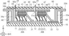
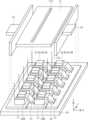
第1実施形態は、半導体モジュールに関する。半導体装置に関する。第1実施形態は、より具体的には、パワー半導体モジュールに関する。図1に実施形態の半導体モジュール100の断面図を示す。図2に実施形態の半導体モジュール100の斜視展開図を示す。図1及び図2には、半導体モジュール100の要部を表している。なお、X方向、Y方向及びZ方向は、互いに交差し、互いに直交することが好ましい。半導体モジュール100は、例えば、風力発電システム、太陽光発電システム及び車両などにおいて、インバータ等の電力変換装置に用いることができるものである。(First embodiment)
The first embodiment relates to a semiconductor module. It relates to a semiconductor device. The first embodiment more specifically relates to a power semiconductor module. FIG. 1 shows a cross-sectional view of a
半導体モジュール100は、基板10と、第1半導体装置20Aと、第2半導体装置20Bと、第1配線層31と、第2配線層32と、第1配線33と、絶縁層41、45と、第1金属膜42、46と、第2金属膜43、47と、接合膜44、48、伝熱板51と、外装材60とを有する。第1半導体装置20Aと第2半導体装置20Bは、基板10及び外装材60で構成されたケース内に配置されている。 The
基板10は、絶縁性の支持体である。基板10の表面には、導電膜11、導電膜12と導電膜13が設けられている。基板10は、セラミック層又は/及び絶縁性の熱伝導性樹脂層を含むことが好ましい。絶縁性の熱伝導性樹脂層は、好ましくは、フィラーを含有する。フィラーは、例えば、窒化ホウ素、アルミナ、窒化アルミ、窒化ケイ素および炭化ケイ素などからなる群より選ばれる1種以上である。基板10は、第1半導体装置20Aや第2半導体装置20Bが発した熱を外部に放熱する部材であって、熱伝導性が高いことが好ましい。基板10は、3W/mK以上の熱伝導性を有することが好ましい。基板10は、17kV/mm以上の絶縁耐圧を有していることが好ましい。基板10上の導電膜11と導電膜12上には、第1半導体装置20A及び第2半導体装置20Bが設けられている。 The
導電膜11、導電膜12及び導電膜13は、CuやAlを含有する導電層である。導電膜11、導電膜12及び導電膜13は、Y方向にも延びている。基板10上で導電膜11、導電膜12及び導電膜13は、それぞれ離間している。導電膜11上に第1半導体装置20A及び第4配線34が設けられていて、電気的に接続している。導電膜12上に第2半導体装置20B及び第1配線層31が設けられ、電気的に接続している。導電膜13上に第2配線層32及び第1配線33が設けられ、電気的に接続している。部材間の接続は、ハンダや導電性ペーストを用いて、部材間を接合することが好ましい。導電膜11と第1半導体装置20Aの接合部分などに用いられる接合部材は図示を省略している。 The
半導体モジュール100は、半導体装置を有する。図1において、半導体モジュール100の左側に第1半導体装置20A、半導体モジュール100の右側に第2半導体装置20Aが位置している。第1半導体装置20Aと第2半導体装置20Bは隣接している。半導体装置は、X方向及びY方向に実装され、1つの半導体モジュールに例えば10個以上の半導体装置が含まれる。第1半導体装置20A及び第2半導体装置20Bは、IGBT(Insulated Gate Bipolar Transistor)又はMOSFETである。第1半導体装置20Aと第2半導体装置20Bは、同じ半導体素子を有することが好ましい。 The
第1実施形態の第1半導体装置20Aは、半導体素子が封止樹脂21で封止されている。第1半導体装置20Aの基板10側を向く面は、第1面である。第1半導体装置20Aの第1面とは反対側の面は第2面である。第1半導体装置20Aの第1面は基板10と対向する。第1半導体装置20Aの第1面は導電膜11と接続している。第1半導体装置20Aは、第1電極22と第2電極23を有する。第1半導体装置20Aの第1面には第1電極22が設けられていて、第1電極22は、導電膜11と電気的に接続している。導電膜11は、第2配線34とも電気的に接続している。第1半導体装置20Aの第2面は第1配線層31と接続している。第1半導体装置20Aの第2面には第2電極23が設けられていて、第2電極23は、第1配線層31と電気的に接続している。第1半導体装置20Aの第1電極22は、例えばエミッタ電極(ソース電極)で、第2電極23は例えばコレクタ電極(ドレイン電極)であるか、又はその逆である。第1半導体装置20Aからは、制御用の第3電極24が延びている。第3電極24は例えばゲート電極である。 In the
第1実施形態の第2半導体装置20Bは、半導体素子が封止樹脂21で封止されている。第2半導体装置20Bの基板10側を向く面は、第1面である。第2半導体装置20Bの第1面とは反対側の面は第2面である。第2半導体装置20Bの第1面は基板10と対向する。第2半導体装置20Bの第1面は導電膜11と接続している。第2半導体装置20Bは、第1電極22と第2電極23を有する。第2半導体装置20Bの第1面には第1電極22が設けられていて、第1電極22は、導電膜12と電気的に接続している。第2半導体装置20Bの第2面は第2配線層32と接続している。第2半導体装置20Bの第2面には第2電極23が設けられていて、第2電極23は、第2配線層32と電気的に接続している。第2半導体装置20Bの第1電極22は、例えばエミッタ電極(ソース電極)で、第2電極23は例えばコレクタ電極(ドレイン電極)であるか、又はその逆である。第2半導体装置20Bからは、制御用の第3電極24が延びている。第3電極24は例えばゲート電極である。 The semiconductor element of the
第1半導体装置20Aと第2半導体装置20Bは、直列に接続している。図2のようにY方向に複数の第1半導体装置20Aが設けられている場合、第Y方向に並んだ第1半導体装置20Aは並列に接続している。図2のようにY方向に複数の第2半導体装置20Bが設けられている場合、第Y方向に並んだ第2半導体装置20Bは並列に接続している。 The
第1半導体装置20Aの第2電極23と第2半導体装置20Bの第1電極22は、第1配線層31を介して電気的に接続し、より具体的には、第1配線層31及び導電膜12を介して電気的に接続している。 The
第1配線層31は、第1半導体装置20Aの第2電極23と第2半導体装置20の第1電極22を電気的に接続する導電性部材である。第1配線層31は、CuやAlを主体とする金属で構成された導電性部材である。 The
第1配線層31は、第1半導体装置20Aの第2電極23から導電膜12に向かって延在している。第1配線層31は、導電膜12の第1半導体装置20A側につながっている。導電膜12は、半導体モジュール100のいわゆるコレクタ兼エミッタ端子と呼ばれる外部端子と接続していてもよい。第1配線層31などの配線は、導電膜12と対向するように面接触する足を設け、導電膜12と超音波接合していてもよい。超音波接合によってハンダなどによる接合よりもより強固に接合することができる。第2配線層32等と他の部材との接合にも超音波接合を採用することが好ましい。 The
第1金属膜42、絶縁層41、第2金属膜43が積層した構造体は、第1配線層31の凹部に接合膜44を介して接続されている。第1金属膜42、絶縁層41、第2金属膜43が積層した構造体は、第1半導体装置20Aの直上に位置していることが好ましい。 A structure in which the
第1配線層31は、第1半導体装置20A側とは反対側の面に凹部を有する。第1配線層31の第1半導体装置20Aと対向する面は平坦面(算術平均粗さが0.01mm以下)であることが好ましい。第1金属膜42、絶縁層41、第2金属膜43が積層した構造体と第1配線層31の接合部分は異種材料が多く、つまり、熱膨張係数の異なる材料が集まっていて、また、半導体モジュール100において主要な熱伝導の経路でもあることから熱応力が大きくなり易い部位である。熱応力が大きくなると、接合膜44が剥離し易くなる。接合膜44が剥離すると第1半導体装置20Aからの熱を放熱し難くなり半導体モジュール100の故障の原因になる可能性がある。 The
そこで、接合膜44への熱応力を緩和するために、第1配線層31の第1半導体装置20A側ではなく、第1半導体装置20A側とは反対側に凹部を設ける。凹部が設けられた部分は剛性が低下し、接合膜44への熱応力の集中を緩和することができる。第1配線層31の第1半導体装置20A側に凹部を設けると、第1配線層31が反り易くなり、反りに伴う応力で接合膜44にストレスがかかって、剥離等の原因になってしまう。 Therefore, in order to relax the thermal stress on the
また、半導体モジュール100内のスペースの制約から第1金属膜42、絶縁層41、第2金属膜43が積層した構造体の面積は、第1配線層31と比べて小さい。第1金属膜42、絶縁層41、第2金属膜43が積層した構造体の第1金属膜42が少なくとも一部埋まる程度の凹部を設ける面積を少なくすることができる。 In addition, due to space restrictions in the
第1配線層31の厚さは、電流容量によって適宜設計され、典型的には0.3mm以上2mm以下である。凹部が設けられていない部分の第1配線層31の厚さは均一であることが好ましい。凹部の第1配線層31の厚さが薄いと、薄くなった部分の電気抵抗が増加してしまうが、接合膜44と第1金属膜42を電流がバイパスできるため、凹部を設けても電気伝導性への影響は小さい。しかし、凹部の第1配線層31が薄すぎると機械的強度が低下して加工がしにくくなる。剛性と機械的強度を考慮すると、第1配線層31の凹部の厚さをd1、第1配線層31の凹部以外の厚さをd2とする場合、d1/d2は、0.5以上0.9以下であることが好ましい。 The thickness of the
電流のバイパスによって、凹部の電気抵抗増加の影響を補う観点から、第1金属膜42の厚さは薄すぎない方がよい。第1金属膜42を必要以上に厚くすると半導体モジュール100のパッケージが厚くなるため好ましくない。そこで、第1配線層31の凹部の厚さをd1、第1配線層31の凹部以外の厚さをd2とする場合第1金属膜42の厚さは、(d2-d1)の0.5倍以上であり、d2の1.0倍以下であることが好ましい。 The thickness of the
第1金属膜42は、CuやAlなどを主体とした導電性の膜である。第1金属膜41は、接合膜44を介して第1配線層31と電気的に接続している。 The
絶縁層41は、熱伝導性に優れる。絶縁層41は3W/mK以上の熱伝導性を有することが好ましい。絶縁層41は、第1半導体装置20Aの第2電極23と熱接続している。絶縁層41は、第1半導体装置20Aから伝熱板51へ熱を伝える伝熱経路に含まれる。絶縁層41は、17kV/mm以上の絶縁耐圧を有していることが好ましい。絶縁層1は、セラミック層又は/及び絶縁性の熱伝導性樹脂層を含むことが好ましい。第1絶縁層41を経る経路で熱を伝えやすくするために、第1絶縁層41の熱伝導率[W/mK]は、第1半導体装置20Aの熱伝導率[W/mK]よりも高いことが好ましい。 The insulating
第2金属膜43は、CuやAlなどを主体とした導電性の膜である。第2金属膜43は、絶縁層41と伝熱板51との間に位置している。第2金属膜43は、絶縁層41及び伝熱板51と接続している。絶縁層41へ伝わった熱は、第2金属膜43を介して伝熱板51に伝わる。 The
接合膜44は、ハンダや導電性ペーストが焼結した導電性部材である。接合膜44は、第1配線層31と第1金属膜42が電気的に接続するように両部材を接合している。接合膜44が薄いと第1金属膜42、絶縁層41、第2金属膜43が積層した構造体を凹部に配置させる際に位置合わせが難しく、また、接合不良になり易い。接合膜44が厚すぎると、ハンダが溶融した時や導電性ペーストを塗布した時に凹部からあふれてショートの原因になる可能性がある。そこで、接合膜44の厚さ(最大厚さ)は凹部の深さである(d1-d2)の0.2倍以上1.0倍以下であることが好ましい。 The
第1金属膜42と絶縁層41の間、又は/及び、第2金属膜43と絶縁層41の間には、導電性又は絶縁性の中間層が含まれていてもよい。 A conductive or insulating intermediate layer may be included between the
第2配線層32は、第2半導体装置20Aの第2電極23と第1配線33を電気的に接続する導電性部材である。第2配線層32は、CuやAlを主体とする金属で構成された導電性部材である。第2配線層32は、導電膜13を介して第1配線33と接続している。 The
第2配線層32と伝熱板51の間にも第1配線層31と伝熱板51の間に設けられている第1金属膜42、絶縁層41、第2金属膜43が積層した構造体の面積と同様の第1金属膜46、絶縁層45、第2金属膜47が積層した構造体の面積が設けられている。第1金属膜46は、接合膜48を介して第2配線層32と接続している。絶縁層45、第1金属膜46、第2金属膜47及び接合膜48は絶縁層41、第1金属膜42、第2金属膜43及び接合膜44と共通するため、その説明を省略する。 A structure in which the
第1配線33は、導電膜13と第2半導体装置20Bの第1電極22と電気的に接続している。第1配線33は、CuやAlを主体とする金属で構成された導電性部材である。第1配線33は、導電膜13と電気的に接続している。第1配線33は、柱部33a又は壁部33aと半導体モジュール100の外部に露出した第2外部電極端子となる端子部34bを有する。第1配線33は、半導体モジュール100の外部に露出した第1外部電極端子となる端子部33cを有するか図示しない電極端子(第1外部電極端子)と接続している。 The
第2配線34は、導電膜11と第1半導体装置20Aの第1電極22と電気的に接続している。第2配線34は、CuやAlを主体とする金属で構成された導電性部材である。第2配線34は、柱部34a又は壁部34aと半導体モジュール100の外部に露出した第2外部電極端子となる端子部34bを有する。第2配線34が端子部34bを有しない場合は、第2配線34は、図示しない第2外部電極端子に接続している。 The
伝熱板51は、第2金属膜43、47と接続している熱伝導性の高い部材である。伝熱板51は電気抵抗が低い部材でも電気抵抗が高い部材でもよい。伝熱板51は、第1配線33、第2配線34及び外装材60からなる群より選ばれる1種以上と熱的に接続し、半導体モジュール100の外部に熱を放出させることが好ましい。この場合、伝熱板51に伝熱した熱は、第1配線33、第2配線34及び外装材60の少なくとも1種に伝熱し、半導体モジュール100の外部に放出される。伝熱板51には、第3電極24を通す開口部51aを設けることができる。 The
外装材60は、第1半導体装置20Aの第3電極24及び第2半導体装置20Bの第3電極24が通る開口部60aを有することが好ましい。外装材60の開口部60aは、例えば絶縁性の樹脂で封止されていることが好ましい。 The
配線に関わる部材は、金属からなる材料で構成されていてもよいし、電気的に接続する面以外の部分に絶縁性で熱伝導性の高い部材を貼り合わせた材料で構成されていてもよい。 The member related to the wiring may be made of a material made of metal, or may be made of a material in which an insulating and highly thermally conductive member is attached to a portion other than the surface to be electrically connected. .
(第2実施形態)
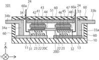
第2実施形態は、半導体モジュールに関する。図3に第2実施形態の半導体モジュール101の断面図を示す。第2実施形態の半導体モジュール101は、半導体素子が樹脂封止された半導体装置に代えて樹脂封止されていないベアチップ(半導体素子)20C、20Dを第1半導体装置20C、第2半導体装置20Dとして用いていて、第2半導体装置20Dの極性が逆であり、第1配線層31と第2配線層32が連結し、連結した第1配線層31と第2配線層32の両端に凹部が設けられていることが第1実施形態の半導体モジュール100と異なる。第1実施形態の半導体モジュール100と第2実施形態の半導体モジュール101で共通する内容については、その説明を省略する。(Second embodiment)
The second embodiment relates to a semiconductor module. FIG. 3 shows a cross-sectional view of the
ベアチップ20C、20Dは、絶縁性の樹脂で封止していない分半導体装置20A及び半導体装置20Bよりも薄いため、半導体モジュール101のパッケージ高さを低くすることができる。実施形態では、パッケージ高さを低くせずに、第2配線34に板部34cを設け、より放熱性の高いパッケージの例を示している。 Since the
ベアチップである半導体素子の表面が第1半導体装置20Cの基板10側の面が第1面であり、第1半導体装置20Cのベアチップの第1面の反対側が第1半導体装置20Cの第1面の第2面である。第1半導体装置20Cの第1面に第1電極22、第2面に第2電極23が設けられている。 The surface of the semiconductor element, which is a bare chip, is the first surface on the side of the
第2半導体装置20Dは、ベアチップである半導体素子の基板10側の面が第2半導体装置20Dの第1面であり、第2半導体装置20Dのベアチップの第1面の反対側が第2半導体装置20Dの第2面である。第2半導体装置20Dは第1半導体装置20Cとは逆の極性になるように基板10に実装されている。第2半導体装置20Dの第1面に第2電極23、第2面に第1電極22が設けられている。 In the
第1配線層31と第2配線層32を連結させることで、第1半導体装置20Cの第2電極23と第2半導体装置20Dの第1電極22を電気的に接続している。 By connecting the
第1配線層31及び第2配線層32の凹部は、図示するようにそれぞれの配線層の先端に設けることができる。 The recesses of the
連結した第1配線層31と第2配線層32の半導体装置側とは反対側に凹部を設けて熱応力を緩和している。従って、半導体モジュール101内の熱応力が緩和される構成となっており、半導体モジュール101の信頼性が高まる。 A concave portion is provided on the side of the connected
本発明のいくつかの実施形態を説明したが、これらの実施形態は、例として提示したものであり、発明の範囲を限定することは意図していない。これら新規な実施形態は、その他の様々な形態で実施されることが可能であり、発明の要旨を逸脱しない範囲で、種々の省略、置き換え、変更を行うことができる。これら実施形態やその変形は、発明の範囲や要旨に含まれるとともに、特許請求の範囲に記載された発明とその均等の範囲に含まれる。 While several embodiments of the invention have been described, these embodiments have been presented by way of example and are not intended to limit the scope of the invention. These novel embodiments can be implemented in various other forms, and various omissions, replacements, and modifications can be made without departing from the scope of the invention. These embodiments and modifications thereof are included in the scope and gist of the invention, and are included in the scope of the invention described in the claims and equivalents thereof.
100、101…半導体モジュール、10…基板、11…導電膜、12…導電膜、13…導電膜、20…半導体装置、21…封止樹脂、22…第1電極、23…第2電極、31…第1配線層、32…第2配線層、33…第1配線、34…第2配線、41…絶縁層、42…第1金属膜、43…第2金属膜、44…接合膜、45…絶縁層、46…第1金属膜、47…第2金属膜、48…接合膜、510…伝熱板、60…外装材DESCRIPTION OF
Claims (9)
Translated fromJapanese前記基板上に設けられ、前記基板側の第1面が前記基板と接続した半導体装置と、
前記半導体装置の前記第1面とは反対側の第2面が接続し、前記半導体装置側とは反対側の面に凹部を有する配線層と、
前記配線層の前記凹部に接合膜を介して設けられ、前記配線層と電気的に接続した第1金属膜と、
前記第1金属膜上に設けられた絶縁層と、
前記絶縁層上に設けられた伝熱板と、
を有する半導体モジュール。a substrate;
a semiconductor device provided on the substrate and having a first surface on the substrate side connected to the substrate;
a wiring layer connected to a second surface of the semiconductor device opposite to the first surface and having a concave portion on a surface opposite to the semiconductor device;
a first metal film provided in the recess of the wiring layer via a bonding film and electrically connected to the wiring layer;
an insulating layer provided on the first metal film;
a heat transfer plate provided on the insulating layer;
A semiconductor module having
d1/d2は、0.5以上0.9以下である請求項1に記載の半導体モジュール。When the thickness of the concave portion of the wiring layer is d1 and the thickness of the portion other than the concave portion is d2,
2. The semiconductor module according to claim 1, wherein d1/d2 is 0.5 or more and 0.9 or less.
前記第1金属膜の厚さは、(d2-d1)の0.5倍以上であり、d2の1.0倍以下である請求項1ないし6のいずれか1項に記載の半導体モジュール。When the thickness of the concave portion of the wiring layer is d1 and the thickness of the portion other than the concave portion is d2,
7. The semiconductor module according to claim 1, wherein the thickness of said first metal film is 0.5 times or more of (d2-d1) and 1.0 times or less of d2.
Priority Applications (2)
| Application Number | Priority Date | Filing Date | Title |
|---|---|---|---|
| JP2020160230AJP7301805B2 (en) | 2020-09-24 | 2020-09-24 | semiconductor module |
| US17/191,272US11476225B2 (en) | 2020-09-24 | 2021-03-03 | Recess portion in the surface of an interconnection layer mounted to a semiconductor device |
Applications Claiming Priority (1)
| Application Number | Priority Date | Filing Date | Title |
|---|---|---|---|
| JP2020160230AJP7301805B2 (en) | 2020-09-24 | 2020-09-24 | semiconductor module |
Publications (2)
| Publication Number | Publication Date |
|---|---|
| JP2022053400A JP2022053400A (en) | 2022-04-05 |
| JP7301805B2true JP7301805B2 (en) | 2023-07-03 |
Family
ID=80740842
Family Applications (1)
| Application Number | Title | Priority Date | Filing Date |
|---|---|---|---|
| JP2020160230AActiveJP7301805B2 (en) | 2020-09-24 | 2020-09-24 | semiconductor module |
Country Status (2)
| Country | Link |
|---|---|
| US (1) | US11476225B2 (en) |
| JP (1) | JP7301805B2 (en) |
Citations (5)
| Publication number | Priority date | Publication date | Assignee | Title |
|---|---|---|---|---|
| JP2003234382A (en) | 2002-02-06 | 2003-08-22 | Shindengen Electric Mfg Co Ltd | Semiconductor device |
| JP2007311441A (en) | 2006-05-17 | 2007-11-29 | Hitachi Ltd | Power semiconductor module |
| JP2016082048A (en) | 2014-10-16 | 2016-05-16 | 三菱電機株式会社 | Semiconductor device |
| JP2017108130A (en) | 2015-11-30 | 2017-06-15 | 株式会社東芝 | Semiconductor module |
| JP2019037047A (en) | 2017-08-11 | 2019-03-07 | 株式会社デンソー | Power converter |
Family Cites Families (8)
| Publication number | Priority date | Publication date | Assignee | Title |
|---|---|---|---|---|
| JP3531133B2 (en) | 1997-02-24 | 2004-05-24 | 同和鉱業株式会社 | Power module substrate and method of manufacturing the same |
| US6703707B1 (en) | 1999-11-24 | 2004-03-09 | Denso Corporation | Semiconductor device having radiation structure |
| DE102004018476B4 (en)* | 2004-04-16 | 2009-06-18 | Infineon Technologies Ag | Power semiconductor arrangement with contacting film and pressing device |
| WO2009125779A1 (en)* | 2008-04-09 | 2009-10-15 | 富士電機デバイステクノロジー株式会社 | Semiconductor device and method for manufacturing semiconductor device |
| JP4634497B2 (en)* | 2008-11-25 | 2011-02-16 | 三菱電機株式会社 | Power semiconductor module |
| JP2015220429A (en)* | 2014-05-21 | 2015-12-07 | ローム株式会社 | Semiconductor device |
| JP2016018866A (en) | 2014-07-08 | 2016-02-01 | 三菱電機株式会社 | Power module |
| DE112017003925B4 (en) | 2016-08-05 | 2022-12-22 | Mitsubishi Electric Corporation | power semiconductor element |
- 2020
- 2020-09-24JPJP2020160230Apatent/JP7301805B2/enactiveActive
- 2021
- 2021-03-03USUS17/191,272patent/US11476225B2/enactiveActive
Patent Citations (6)
| Publication number | Priority date | Publication date | Assignee | Title |
|---|---|---|---|---|
| JP2003234382A (en) | 2002-02-06 | 2003-08-22 | Shindengen Electric Mfg Co Ltd | Semiconductor device |
| JP2007311441A (en) | 2006-05-17 | 2007-11-29 | Hitachi Ltd | Power semiconductor module |
| JP2016082048A (en) | 2014-10-16 | 2016-05-16 | 三菱電機株式会社 | Semiconductor device |
| JP2017108130A (en) | 2015-11-30 | 2017-06-15 | 株式会社東芝 | Semiconductor module |
| JP2019037047A (en) | 2017-08-11 | 2019-03-07 | 株式会社デンソー | Power converter |
| US20200176354A1 (en) | 2017-08-11 | 2020-06-04 | Denso Corporation | Power conversion apparatus |
Also Published As
| Publication number | Publication date |
|---|---|
| US11476225B2 (en) | 2022-10-18 |
| US20220093554A1 (en) | 2022-03-24 |
| JP2022053400A (en) | 2022-04-05 |
Similar Documents
| Publication | Publication Date | Title |
|---|---|---|
| JP6786416B2 (en) | Semiconductor device | |
| CN108735692B (en) | Semiconductor device with a semiconductor device having a plurality of semiconductor chips | |
| JP7391957B2 (en) | semiconductor equipment | |
| US11742333B2 (en) | Semiconductor module | |
| JPH11204700A (en) | Power module with integrated radiation fins | |
| JP7354076B2 (en) | semiconductor module | |
| JP2007123884A (en) | Power circuit package and method of fabricating same | |
| US20030090915A1 (en) | Inverter apparatus and method of manufacturing the same | |
| WO2020241239A1 (en) | Semiconductor device | |
| JP7163583B2 (en) | semiconductor equipment | |
| WO2019235146A1 (en) | Semiconductor module | |
| JP6248803B2 (en) | Power semiconductor module | |
| JP4645406B2 (en) | Semiconductor device | |
| JP4805636B2 (en) | Power semiconductor device and semiconductor power converter | |
| JP7301805B2 (en) | semiconductor module | |
| JP2010225952A (en) | Semiconductor module | |
| JP2023168849A (en) | Semiconductor device and manufacturing method for the same | |
| JP3855726B2 (en) | Power module | |
| CN113597671B (en) | Semiconductor device with a semiconductor device having a plurality of semiconductor chips | |
| WO2023017708A1 (en) | Semiconductor device | |
| JP2023134143A (en) | Semiconductor module, semiconductor device, and vehicle | |
| JP7681920B2 (en) | Semiconductor package and manufacturing method thereof | |
| JP6887476B2 (en) | Semiconductor power module | |
| WO2024018851A1 (en) | Semiconductor device | |
| JP2025151720A (en) | Power Semiconductor Module |
Legal Events
| Date | Code | Title | Description |
|---|---|---|---|
| A621 | Written request for application examination | Free format text:JAPANESE INTERMEDIATE CODE: A621 Effective date:20220705 | |
| A977 | Report on retrieval | Free format text:JAPANESE INTERMEDIATE CODE: A971007 Effective date:20230427 | |
| TRDD | Decision of grant or rejection written | ||
| A01 | Written decision to grant a patent or to grant a registration (utility model) | Free format text:JAPANESE INTERMEDIATE CODE: A01 Effective date:20230523 | |
| A61 | First payment of annual fees (during grant procedure) | Free format text:JAPANESE INTERMEDIATE CODE: A61 Effective date:20230621 | |
| R150 | Certificate of patent or registration of utility model | Ref document number:7301805 Country of ref document:JP Free format text:JAPANESE INTERMEDIATE CODE: R150 |