JP7301727B2 - Plasma processing apparatus and plasma processing method - Google Patents
Plasma processing apparatus and plasma processing methodDownload PDFInfo
- Publication number
- JP7301727B2 JP7301727B2JP2019220668AJP2019220668AJP7301727B2JP 7301727 B2JP7301727 B2JP 7301727B2JP 2019220668 AJP2019220668 AJP 2019220668AJP 2019220668 AJP2019220668 AJP 2019220668AJP 7301727 B2JP7301727 B2JP 7301727B2
- Authority
- JP
- Japan
- Prior art keywords
- dielectric plate
- plasma processing
- plasma
- outer peripheral
- processing apparatus
- Prior art date
- Legal status (The legal status is an assumption and is not a legal conclusion. Google has not performed a legal analysis and makes no representation as to the accuracy of the status listed.)
- Active
Links
Images


Classifications
- H—ELECTRICITY
- H01—ELECTRIC ELEMENTS
- H01J—ELECTRIC DISCHARGE TUBES OR DISCHARGE LAMPS
- H01J37/00—Discharge tubes with provision for introducing objects or material to be exposed to the discharge, e.g. for the purpose of examination or processing thereof
- H01J37/32—Gas-filled discharge tubes
- H01J37/32431—Constructional details of the reactor
- H01J37/32532—Electrodes
- H01J37/32541—Shape
- C—CHEMISTRY; METALLURGY
- C23—COATING METALLIC MATERIAL; COATING MATERIAL WITH METALLIC MATERIAL; CHEMICAL SURFACE TREATMENT; DIFFUSION TREATMENT OF METALLIC MATERIAL; COATING BY VACUUM EVAPORATION, BY SPUTTERING, BY ION IMPLANTATION OR BY CHEMICAL VAPOUR DEPOSITION, IN GENERAL; INHIBITING CORROSION OF METALLIC MATERIAL OR INCRUSTATION IN GENERAL
- C23C—COATING METALLIC MATERIAL; COATING MATERIAL WITH METALLIC MATERIAL; SURFACE TREATMENT OF METALLIC MATERIAL BY DIFFUSION INTO THE SURFACE, BY CHEMICAL CONVERSION OR SUBSTITUTION; COATING BY VACUUM EVAPORATION, BY SPUTTERING, BY ION IMPLANTATION OR BY CHEMICAL VAPOUR DEPOSITION, IN GENERAL
- C23C16/00—Chemical coating by decomposition of gaseous compounds, without leaving reaction products of surface material in the coating, i.e. chemical vapour deposition [CVD] processes
- C23C16/22—Chemical coating by decomposition of gaseous compounds, without leaving reaction products of surface material in the coating, i.e. chemical vapour deposition [CVD] processes characterised by the deposition of inorganic material, other than metallic material
- C23C16/30—Deposition of compounds, mixtures or solid solutions, e.g. borides, carbides, nitrides
- C23C16/34—Nitrides
- C23C16/345—Silicon nitride
- C—CHEMISTRY; METALLURGY
- C23—COATING METALLIC MATERIAL; COATING MATERIAL WITH METALLIC MATERIAL; CHEMICAL SURFACE TREATMENT; DIFFUSION TREATMENT OF METALLIC MATERIAL; COATING BY VACUUM EVAPORATION, BY SPUTTERING, BY ION IMPLANTATION OR BY CHEMICAL VAPOUR DEPOSITION, IN GENERAL; INHIBITING CORROSION OF METALLIC MATERIAL OR INCRUSTATION IN GENERAL
- C23C—COATING METALLIC MATERIAL; COATING MATERIAL WITH METALLIC MATERIAL; SURFACE TREATMENT OF METALLIC MATERIAL BY DIFFUSION INTO THE SURFACE, BY CHEMICAL CONVERSION OR SUBSTITUTION; COATING BY VACUUM EVAPORATION, BY SPUTTERING, BY ION IMPLANTATION OR BY CHEMICAL VAPOUR DEPOSITION, IN GENERAL
- C23C16/00—Chemical coating by decomposition of gaseous compounds, without leaving reaction products of surface material in the coating, i.e. chemical vapour deposition [CVD] processes
- C23C16/44—Chemical coating by decomposition of gaseous compounds, without leaving reaction products of surface material in the coating, i.e. chemical vapour deposition [CVD] processes characterised by the method of coating
- C23C16/50—Chemical coating by decomposition of gaseous compounds, without leaving reaction products of surface material in the coating, i.e. chemical vapour deposition [CVD] processes characterised by the method of coating using electric discharges
- C23C16/505—Chemical coating by decomposition of gaseous compounds, without leaving reaction products of surface material in the coating, i.e. chemical vapour deposition [CVD] processes characterised by the method of coating using electric discharges using radio frequency discharges
- C23C16/509—Chemical coating by decomposition of gaseous compounds, without leaving reaction products of surface material in the coating, i.e. chemical vapour deposition [CVD] processes characterised by the method of coating using electric discharges using radio frequency discharges using internal electrodes
- H—ELECTRICITY
- H01—ELECTRIC ELEMENTS
- H01J—ELECTRIC DISCHARGE TUBES OR DISCHARGE LAMPS
- H01J37/00—Discharge tubes with provision for introducing objects or material to be exposed to the discharge, e.g. for the purpose of examination or processing thereof
- H01J37/32—Gas-filled discharge tubes
- H01J37/32431—Constructional details of the reactor
- H01J37/32532—Electrodes
- H01J37/3255—Material
- H—ELECTRICITY
- H01—ELECTRIC ELEMENTS
- H01L—SEMICONDUCTOR DEVICES NOT COVERED BY CLASS H10
- H01L21/00—Processes or apparatus adapted for the manufacture or treatment of semiconductor or solid state devices or of parts thereof
- H01L21/02—Manufacture or treatment of semiconductor devices or of parts thereof
- H01L21/04—Manufacture or treatment of semiconductor devices or of parts thereof the devices having potential barriers, e.g. a PN junction, depletion layer or carrier concentration layer
- H01L21/18—Manufacture or treatment of semiconductor devices or of parts thereof the devices having potential barriers, e.g. a PN junction, depletion layer or carrier concentration layer the devices having semiconductor bodies comprising elements of Group IV of the Periodic Table or AIIIBV compounds with or without impurities, e.g. doping materials
- H01L21/30—Treatment of semiconductor bodies using processes or apparatus not provided for in groups H01L21/20 - H01L21/26
- H01L21/302—Treatment of semiconductor bodies using processes or apparatus not provided for in groups H01L21/20 - H01L21/26 to change their surface-physical characteristics or shape, e.g. etching, polishing, cutting
- H01L21/306—Chemical or electrical treatment, e.g. electrolytic etching
- H01L21/3065—Plasma etching; Reactive-ion etching
- H—ELECTRICITY
- H01—ELECTRIC ELEMENTS
- H01L—SEMICONDUCTOR DEVICES NOT COVERED BY CLASS H10
- H01L21/00—Processes or apparatus adapted for the manufacture or treatment of semiconductor or solid state devices or of parts thereof
- H01L21/02—Manufacture or treatment of semiconductor devices or of parts thereof
- H01L21/04—Manufacture or treatment of semiconductor devices or of parts thereof the devices having potential barriers, e.g. a PN junction, depletion layer or carrier concentration layer
- H01L21/18—Manufacture or treatment of semiconductor devices or of parts thereof the devices having potential barriers, e.g. a PN junction, depletion layer or carrier concentration layer the devices having semiconductor bodies comprising elements of Group IV of the Periodic Table or AIIIBV compounds with or without impurities, e.g. doping materials
- H01L21/30—Treatment of semiconductor bodies using processes or apparatus not provided for in groups H01L21/20 - H01L21/26
- H01L21/31—Treatment of semiconductor bodies using processes or apparatus not provided for in groups H01L21/20 - H01L21/26 to form insulating layers thereon, e.g. for masking or by using photolithographic techniques; After treatment of these layers; Selection of materials for these layers
- H—ELECTRICITY
- H05—ELECTRIC TECHNIQUES NOT OTHERWISE PROVIDED FOR
- H05H—PLASMA TECHNIQUE; PRODUCTION OF ACCELERATED ELECTRICALLY-CHARGED PARTICLES OR OF NEUTRONS; PRODUCTION OR ACCELERATION OF NEUTRAL MOLECULAR OR ATOMIC BEAMS
- H05H1/00—Generating plasma; Handling plasma
- H05H1/24—Generating plasma
- H05H1/46—Generating plasma using applied electromagnetic fields, e.g. high frequency or microwave energy
- H—ELECTRICITY
- H01—ELECTRIC ELEMENTS
- H01J—ELECTRIC DISCHARGE TUBES OR DISCHARGE LAMPS
- H01J2237/00—Discharge tubes exposing object to beam, e.g. for analysis treatment, etching, imaging
- H01J2237/32—Processing objects by plasma generation
- H01J2237/33—Processing objects by plasma generation characterised by the type of processing
- H01J2237/332—Coating
- H01J2237/3321—CVD [Chemical Vapor Deposition]
- H—ELECTRICITY
- H01—ELECTRIC ELEMENTS
- H01J—ELECTRIC DISCHARGE TUBES OR DISCHARGE LAMPS
- H01J2237/00—Discharge tubes exposing object to beam, e.g. for analysis treatment, etching, imaging
- H01J2237/32—Processing objects by plasma generation
- H01J2237/33—Processing objects by plasma generation characterised by the type of processing
- H01J2237/334—Etching
- H—ELECTRICITY
- H01—ELECTRIC ELEMENTS
- H01J—ELECTRIC DISCHARGE TUBES OR DISCHARGE LAMPS
- H01J37/00—Discharge tubes with provision for introducing objects or material to be exposed to the discharge, e.g. for the purpose of examination or processing thereof
- H01J37/32—Gas-filled discharge tubes
- H01J37/32009—Arrangements for generation of plasma specially adapted for examination or treatment of objects, e.g. plasma sources
- H01J37/32082—Radio frequency generated discharge
Landscapes
- Chemical & Material Sciences (AREA)
- Engineering & Computer Science (AREA)
- Physics & Mathematics (AREA)
- Plasma & Fusion (AREA)
- Analytical Chemistry (AREA)
- Organic Chemistry (AREA)
- Chemical Kinetics & Catalysis (AREA)
- Materials Engineering (AREA)
- Mechanical Engineering (AREA)
- Metallurgy (AREA)
- General Chemical & Material Sciences (AREA)
- Computer Hardware Design (AREA)
- General Physics & Mathematics (AREA)
- Manufacturing & Machinery (AREA)
- Condensed Matter Physics & Semiconductors (AREA)
- Microelectronics & Electronic Packaging (AREA)
- Power Engineering (AREA)
- Electromagnetism (AREA)
- Spectroscopy & Molecular Physics (AREA)
- Inorganic Chemistry (AREA)
- Drying Of Semiconductors (AREA)
- Plasma Technology (AREA)
- Chemical Vapour Deposition (AREA)
Description
Translated fromJapanese本開示は、プラズマ処理装置及びプラズマ処理方法に関する。 The present disclosure relates to a plasma processing apparatus and a plasma processing method.
例えば、特許文献1は、真空容器のなかで向かい合う2つの電極面の間で形成されるプラズマプロセス空間で高周波プラズマが生成され、一方の電極面は誘電性材料からできており、誘電性材料は、厚みが周辺領域で中心領域よりも小さくなる構成を提案している。 For example,
また、例えば、特許文献2は、上部電極は、下部電極に対向する電極板を備え、電極板は、導電体または半導体で構成された外側部分と、誘電体部材または外側部分より高抵抗の高抵抗部材で構成された中間部分とを有する構成を提案している。上部電極には、その下部電極と反対側の面から高周波電力が印加される。 Further, for example, in Patent Document 2, the upper electrode includes an electrode plate facing the lower electrode, and the electrode plate includes an outer portion made of a conductor or a semiconductor and a dielectric member or a high-resistance material having a higher resistance than the outer portion. An intermediate portion made up of a resistive member is proposed. High-frequency power is applied to the upper electrode from the surface opposite to the lower electrode.
本開示は、プラズマ密度の面内均一性を向上させることができるプラズマ処理装置及びプラズマ処理方法を提供する。 The present disclosure provides a plasma processing apparatus and a plasma processing method capable of improving in-plane uniformity of plasma density.
本開示の一の態様によれば、処理容器内に設けられた載置台と上部電極とを有するプラズマ処理装置であって、前記上部電極は、前記載置台と対向する誘電体板と、前記誘電体板の前記載置台に対向する面の反対側に形成された導体と、を有し、前記誘電体板は、中心部と、外周部と、前記中心部と前記外周部との間の中間部とを有し、前記中間部の厚さは、前記中心部と前記外周部との厚さよりも厚い、プラズマ処理装置が提供される。 According to one aspect of the present disclosure, there is provided a plasma processing apparatus having a mounting table provided in a processing container and an upper electrode, wherein the upper electrode includes a dielectric plate facing the mounting table and the dielectric and a conductor formed on the opposite side of the surface of the body plate facing the mounting table, wherein the dielectric plate includes a central portion, an outer peripheral portion, and an intermediate portion between the central portion and the outer peripheral portion. and a portion, wherein the thickness of the intermediate portion is thicker than the thickness of the central portion and the outer peripheral portion.
一の側面によれば、プラズマ密度の面内均一性を向上させることができる。 According to one aspect, in-plane uniformity of plasma density can be improved.
以下、図面を参照して本開示を実施するための形態について説明する。各図面において、同一構成部分には同一符号を付し、重複した説明を省略する場合がある。 Hereinafter, embodiments for carrying out the present disclosure will be described with reference to the drawings. In each drawing, the same components are denoted by the same reference numerals, and redundant description may be omitted.
[プラズマ処理装置]
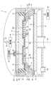
まず、実施形態に係るプラズマ処理装置1について、図1を参照しながら説明する。図1は、実施形態に係るプラズマ処理装置1を示す断面模式図である。図1に示すプラズマ処理装置1は、処理容器10、載置台12、上部電極14、及び導波部20を有する。[Plasma processing equipment]
First, a
処理容器10は、略円筒形状を有し、鉛直方向に沿って延在している。処理容器10の中心軸線は、鉛直方向に延びる軸線AXである。処理容器10は、アルミニウム又はアルミニウム合金といった導体から形成されている。処理容器10の表面上には、耐腐食性を有する膜が形成されている。耐腐食性を有する膜は、例えば酸化アルミニウム又は酸化イットリウムといったセラミックスである。処理容器10は、接地されている。 The
載置台12は、処理容器10内に設けられている。載置台12は、その上面に載置された基板Wを略水平に支持するように構成されている。載置台12は、略円盤形状を有している。載置台12の中心軸線は、軸線AXに略一致している。 The mounting table 12 is provided inside the
プラズマ処理装置1は、バッフル部材13を更に備えていてもよい。バッフル部材13は、載置台12と処理容器10の側壁との間で延在している。バッフル部材13は、略環状の板材である。バッフル部材13は、例えば、酸化アルミニウムといった絶縁体から形成されている。バッフル部材13には、複数の貫通孔が形成されている。複数の貫通孔は、バッフル部材13をその板厚方向に貫通している。載置台12の下方において処理容器10には、排気口10eが形成されている。排気口10eには、排気装置が接続されている。排気装置は、圧力制御弁並びにターボ分子ポンプ及び/又はドライポンプといった真空ポンプを含んでいる。排気装置により、処理容器10内を真空引きする。 The
上部電極14は、処理容器10内のプラズマ処理空間(以下、空間SPという。)を介して載置台12の上方に設けられている。上部電極14の中心軸線は、軸線AXに略一致している。上部電極14は、略円盤形状を有している。上部電極14は、誘電体板18と導体17とを有する。載置台12と誘電体板18とは対向し、載置台12と誘電体板18との間の空間SPにてプラズマが生成される。 The
誘電体板18は、例えばセラミックスから形成され、高周波(電磁波)を透過する。誘電体板18の下面は空間SPに露出し、誘電体板18を透過した電磁波は空間SPに放射される。導体17は、誘電体板18の空間SPに露出する面の反対面に形成される。導体17は、金属メッシュ又は金属膜で形成されてもよい。導体17の材料は、タングステンまたはモリブデンであるが、他の導電性材料であってもよい。上部電極14は、さらに基台19を有し、基台19は、導体17を挟んで誘電体板18の反対側に設けられる。基台19は、アルミニウム等の金属であってもよい。ただし、基台19は金属に限られず、その他の材料で形成されてもよい。また、導体17を設けない場合には、基台19の誘電体板18との接触面を導体17として扱うことができる。上部電極14の中心軸線は、軸線AXに略一致している。 The
円筒部材24は、略円筒形状を有し、アルミニウム又はアルミニウム合金といった導体から形成されている。円筒部材24の中心軸線は、軸線AXに略一致している。円筒部材24は、鉛直方向に延在している。円筒部材24の下端面は、処理容器10の上端面に接触する。処理容器10は接地されている。したがって、円筒部材24は、接地されている。円筒部材24の上端には、基台19の上面と共に導波通路rを構成する上壁部221が位置している。 The
プラズマ処理装置1は、空間SPに高周波を供給するために導波部20(導波通路r)を備えている。導波部20は、上部電極14の周縁部の外側に導波路15を有する。導波路15は、高周波を空間SPに導入する部分である。高周波は、VHF波である。導波路15は、空間SPの横方向端部に設けられている。 The
導波路15は、鉛直方向に沿って延びる円筒状の部材である。導波路15の中心軸線は、軸線AXに略一致している。導波路15は、石英、テフロン(登録商標)等の誘電体から形成されている。なお、導波路15は、空間であってもよい。導波部20は更に導波路201を有する。導波路201は、上部電極14の上面と円筒部材24の上壁面との間の空間によって提供されており、これらはアルミニウム又はアルミニウム合金といった導体から構成することができる。 The
導波部20の内壁を構成する上部電極14の上面には、高周波電源30が、整合器32を介して電気的に接続されている。高周波電源30は、高周波を発生する電源である。整合器32は、高周波電源30から見た負荷側のインピーダンスを高周波電源30の出力インピーダンスに整合させるための整合回路を含んでいる。 A high-
プラズマ処理装置1では、高周波は、高周波電源30から導波部20の導波路201及び導波路15を介して誘電体板18の外周側に伝播し、誘電体板18を透過して誘電体板18の下面から空間SPに供給される。高周波はVHF波である。高周波はUHF波でもよい。 In the
円筒部材24の下面と処理容器10の本体の上端面との間には、封止部材25が介在している。導波路15の下面と処理容器10の本体の上端面との間には、封止部材125が介在している。封止部材25及び封止部材125の各々は、弾性を有し、例えば、ゴム製のOリングである。封止部材25及び封止部材125の各々は、軸線AXの周りで周方向に延在している。なお、導波路15の下面は、処理容器10の本体の上端面で覆われることなく、空間SPに開放された形態であってもよい。この場合、導波路15の下面近傍の処理容器10の傾斜面の位置を、導波路15の下端が処理空間SPに露出する位置まで削った形態にし、封止部材125は配置しなくてもよい。 A sealing
基台19の下面と誘電体板18(及び導体17)との間には、ガス拡散用の空間225が画成されている。空間225には、配管40が接続されている。配管40には、ガス供給器42が接続されている。ガス供給器42は、基板Wの処理のために用いられる一つ以上のガス源を含む。また、ガス供給器42は、一つ以上のガス源からのガスの流量をそれぞれ制御するための一つ以上の流量制御器を含む。 A
配管40は、空間225に延びている。導波部20が提供する導波路201は、接地された導体によって構成されている。したがって、配管40内でガスが励起されることが抑制される。空間225に供給されたガスは、誘電体板18の複数のガス吐出孔18hを介して、空間SPに吐出される。 The
誘電体板18の厚みは略逆W字形状(外周部が薄く、中間部が厚く、中央部が薄い)になっている。これにより、高周波による電界を均一に空間SP内に形成することができる。空間SPに形成された高周波の電界により、ガスが空間SP内で励起されて、当該ガスからプラズマが生成される。これにより、プラズマは、空間SP内で均一な密度分布で生成される。載置台12上の基板Wは、プラズマからの化学種によって処理される。 The
なお、載置台12には、静電チャック用の導電層と、ヒータ用の導電層が設けられている。載置台12は、本体と、静電チャック用の導電層と、ヒータ用の導電層とを有している。載置台12は、下部電極として機能させるためのアルミニウムなどの導電体としてもよいが、一例としては、窒化アルミニウムといった絶縁体から形成されている。載置台12は、略円盤形状を有している。載置台の導電層は、導電性を有する材料、例えばタングステンから形成されている。この導電層は、本体内に設けられている。直流電源からの直流電圧が、静電チャック用の導電層に印加されると、載置台12と基板Wとの間で静電引力が発生する。発生した静電引力により、基板Wは、載置台12に引き付けられ、載置台12によって保持される。別の実施形態において、この導電層は、高周波電極であってもよい。この場合には、導電層には、高周波電源が整合器を介して電気的に接続される。更に別の実施形態において、導電層は、接地される電極であってもよい。このような絶縁体に埋め込まれた導電層は、上部電極との間の電界を形成するための下部電極としても機能させることができる。 The mounting table 12 is provided with a conductive layer for an electrostatic chuck and a conductive layer for a heater. The mounting table 12 has a main body, a conductive layer for an electrostatic chuck, and a conductive layer for a heater. The mounting table 12 may be made of a conductor such as aluminum for functioning as a lower electrode, but is made of an insulator such as aluminum nitride as an example. The mounting table 12 has a substantially disk shape. The conductive layer of the mounting table is made of a conductive material such as tungsten. The conductive layer is provided within the body. When a DC voltage from a DC power supply is applied to the conductive layer for electrostatic chuck, electrostatic attraction is generated between the mounting table 12 and the substrate W. As shown in FIG. The substrate W is attracted to the mounting table 12 and held by the mounting table 12 due to the generated electrostatic attraction. In another embodiment, this conductive layer may be a radio frequency electrode. In this case, a high frequency power supply is electrically connected to the conductive layer through a matching box. In yet another embodiment, the conductive layer may be an electrode that is grounded. A conductive layer embedded in such an insulator can also function as a lower electrode for forming an electric field with the upper electrode.
[誘電体板]
実施形態においては、上部電極14の基台19の下に、ガス拡散用の空間225を介して、誘電体板18が配置される。基台19の下面は、中心と外周が凸状になり、中間はリング状に凹んでいる。基台19の下に形成されたガス拡散用の空間225は、基台19の下面に沿って中心と外周が凹み、中間が凸状になっている。空間225には、ガス供給器42からのガスが流通する。ガス拡散用の空間225は、水平方向にガスが拡散するように連通している。[Dielectric plate]
In the embodiment, a
実施形態において、ガス拡散用の空間225の下方の誘電体板18には、複数のガス吐出孔18hが形成されている。ガス吐出孔18hは、ガス供給器42からのガスを空間SPに吐出するガス供給用の貫通孔である。複数のガス吐出孔18hの各々は、誘電体板18の上面から下面に至るまで誘電体板を貫通している。複数のガス吐出孔の各々は、上部孔18h1と下部孔18h2とを備える。上部孔18h1は、誘電体板18の上面側に設けられ、下部孔18h2は、誘電体板18の下面側に設けられる。上部孔18h1の径は、下部孔18h2の径よりも大きい。In the embodiment, a plurality of gas ejection holes 18h are formed in the
複数のガス吐出孔18hの各々において、下部孔18h2は、上部孔18h1の下方に延びており、上部孔18h1に連通している。上部孔18h1は、空間225に連通している。下部孔18h2は、空間SPに連通している。複数のガス吐出孔18hは、それらが形成されている箇所の誘電体板18の厚みの大きさに応じて長さが大きくなるように調整された大径の上部孔18h1を有する。複数のガス吐出孔18hにおいて、複数の下部孔18h2の長さL1は略同一である。In each of the plurality of
誘電体板18の材料はセラミックスである。誘電体板18を構成する材料は、窒化アルミニウム(AlN)、酸化アルミニウム(Al2O3)及び酸化イットリウム(Y2O3)からなる誘電体群のうち少なくともいずれか一種を含むことができる。本例では窒化アルミニウムであるとするが、誘電体板18の材料としては、他の材料を用いることもできる。 The material of the
誘電体板18の上面には、上部電極として機能する導体17が設けられている。導体17には、グランド電位との間に、高周波電圧が与えられる。導体17の材料は、例えば、アルミニウム、ニッケル、ステンレス、タングステン、モリブデン、銅、又は金である。導体17を構成する導電膜材料は、溶射法、スパッタ法又は化学的気相成長(CVD:Chemical Vapor Deposition)法によって、誘電体板18の上面上に堆積することができる。 A
なお、シャワープレートを構成する誘電体板18の少なくとも下面には、耐腐食性を有する膜が形成されていてもよい。耐腐食性を有する膜は、酸化イットリウム膜、オキシフッ化イットリウム及びフッ化イットリウムからなる群のうち少なくともいずれか一種を含むことができる。耐腐食性を有する膜は、その他のセラミックス材料を用いることもできる。 A corrosion-resistant film may be formed on at least the lower surface of the
図2は、実施形態に係る誘電体板18の上面を示す図である。誘電体板18は、平面視において、中心部Ra、中間部Rb、外周部Rcの3つの領域を有している。中間部Rbは、中心部Raと外周部Rcとの間に位置する。つまり、中心部Raを囲むように中間部Rbが同心円状に配置され、中間部Rbを囲むように外周部Rcが同心円状に配置されている。 FIG. 2 is a diagram showing the top surface of the
図1に示すように、中心部Raの上面及び下面は平坦であり、一定の厚みを有する。中間部Rbの上面及び下面は、平坦であり、一定の厚みを有する。外周部Rcの上面及び下面は、平坦であり、一定の厚みを有する。中間部Rbの厚さは、中心部Raと外周部Rcとの厚さよりも厚い。実施形態では、中心部Raと外周部Rcの厚さは、同一である。ただし、これに限られず、中心部Raと外周部Rcの厚さは異なっていてもよい。 As shown in FIG. 1, the upper and lower surfaces of the central portion Ra are flat and have a constant thickness. The upper and lower surfaces of intermediate portion Rb are flat and have a constant thickness. The upper and lower surfaces of outer peripheral portion Rc are flat and have a constant thickness. The thickness of the intermediate portion Rb is thicker than the thicknesses of the central portion Ra and the outer peripheral portion Rc. In the embodiment, the central portion Ra and the outer peripheral portion Rc have the same thickness. However, the thickness is not limited to this, and the thicknesses of the central portion Ra and the outer peripheral portion Rc may be different.
かかる構成により、誘電体板18の厚みは、略逆W字型に形成されている。具体的には、誘電体板18の上面は、中心部Raと外周部Rcとが、中間部Rbに対して低くなる段差を有している。誘電体板18の厚みを略逆W字に形成することで、プラズマ密度の面内均一性を向上させることができる。なお、実施形態では、中心部Raと中間部Rbとの段差は垂直に形成されているが、これに限られず階段状に形成されてもよく、緩やかな傾斜状に形成されてもよい。また、中間部Rbと外周部Rcとの段差は垂直に形成されているが、これに限られず階段状に形成されてもよく、緩やかな傾斜状に形成されてもよい。 With such a configuration, the thickness of the
図3(a)~図3(c)は、軸AXを右端にして左半分の誘電体板及びその周辺の上部電極14及び導波部20を示す。図3(a)は、比較例に係る誘電体板180を示す。比較例に係る誘電体板180の上面は凸レンズ形状であり、中心から外周に向かってなだらかに下降する傾斜を有する。図3(b)は、実施形態に係る誘電体板18の形状を示す。図3(c)は、実施形態の変形例に係る誘電体板18の形状を示す。 3(a) to 3(c) show the left half of the dielectric plate with the axis AX as the right end, and the
実施形態及び変形例に係る誘電体板18は、比較例に係る誘電体板180と比べてプラズマ密度の面内均一性を向上させることができる。これを証明するシミュレーション結果とその理由について説明する。最初に、上部電極14の下面(プラズマ形成面)に金属板を設けた場合(図示省略)について説明する。この場合、金属の下面を伝播する表面波プラズマに高次のモードが出現するために、プラズマ密度分布が不均一になる。 The
そこで、比較例では、図3(a)に示すように上部電極14の下面に金属板に替えてセラミックスの誘電体板180を設ける。これにより、誘電体板180の下面を伝播する表面波プラズマに高次のモードが出現することを抑制することができる。 Therefore, in a comparative example, a ceramic
しかしながら、これによればプラズマ密度分布の均一性に改善が得られるものの、完全にプラズマ密度の面内均一性が図れるまでには至っていなかった。図3(d)~(f)は、誘電体板180及び誘電体板18の中心0から径方向に150mmまでの位置x(mm)とE2(E:電界)で示される電界エネルギーとの関係を示すグラフである。電界Eは、誘電体板18の下に形成されるシース電界である。However, according to this, although the uniformity of the plasma density distribution can be improved, the in-plane uniformity of the plasma density has not been achieved completely. 3(d) to (f) show the relationship between the position x (mm) from the
図3(d)~(f)のシミュレーション結果を得るために、高周波電源としてVHF波を用い、基台19にプラズマ生成用の高周波を印加した。誘電体板18及び誘電体板180の直径は300mm、材料はAlNである。図3(b)の誘電体板18の中間部Rbの厚みは2.0cm、中心部Ra及び外周部Rcの厚みは0.5cmである。導体17はAlの溶射により形成した。比較例では、実施形態と異なり、誘電体板180の厚みは中心部が2.0cm、外周部が0.5mmであり、中心から外周に向かってなだらかに傾斜する。 In order to obtain the simulation results shown in FIGS. 3(d) to 3(f), a VHF wave was used as the high frequency power supply, and a high frequency for plasma generation was applied to the
図3(d)のグラフから明らかなように、図3(a)に示す比較例の誘電体板180では、電界エネルギーE2の値は、外周部が高く中心部に行くほど低くなった。電界エネルギーE2は、プラズマ密度と相関関係がある。電界エネルギーE2は、径方向のある位置における電界エネルギーの高さ方向(上部電極14と載置台12の間)の積算分布であり、この積算分布がプラズマ密度分布とほぼ一致する。よって、図3(a)に示す比較例の誘電体板180では、プラズマ密度分布の均一性が図れるまでには至っていないことがわかる。As is clear from the graph of FIG. 3(d), in the
これに対して、図3(b)に示す実施形態に係る誘電体板18では、厚みを略逆W字型にした。これにより、図3(e)のグラフに示すように、誘電体板18の中心0から径方向に150mmまでの領域にて電界エネルギーE2が均一になる。これにより、実施形態に係る誘電体板18では、直径300mmの基板Wの上方にてプラズマ密度分布の均一性が図れることがわかった。On the other hand, the
誘電体板18の厚みを略逆W字型にすることでなぜプラズマ密度分布の均一性が図れるのかについて、2つの理由を説明する。まず一つ目の理由であるが、プラズマの密度分布は、プラズマ中の電界分布で決まる。誘電体板18の替わりに金属(導体)を使用した場合、上部電極14の外側の導波路15から伝播する高周波の電界は、軸AXにて示す中心まで届かない。このため中心部の電界を高くするためには、誘電体板18の材質をセラミックス等の誘電体にする。これにより、高周波が誘電体の内部を透過することで高周波の電界が全体的に届きやすくなる。 There are two reasons why the uniformity of the plasma density distribution can be achieved by making the thickness of the
更に、誘電体板18の厚みを略逆W字形状にし、下面を平坦にすることで、中心部Ra及び外周部Rcを中間部Rbよりも薄くする。これにより、高周波の通る誘電体板18の経路が、中心部Ra及び外周部Rcでは中間部Rbよりも狭くなる。中心部Raまで高周波を伝播させるためには、中心部Raに向かう途中の中間部Rbの経路はある程度広くして、高周波が通り易いようにしておく。 Further, the thickness of the
また、外周部Rcの厚さは、中間部Rbの厚さよりも薄くする。これは、高周波が外周側から中心に向かって伝播するため、外周部Rcは中間部Rbよりも電界が強くなり易い。よって、外周部Rcと中間部Rbとを同じ厚さにすると、外周部Rcにおいて中間部Rbよりも強い電界が生じ、外周部Rcから中間部Rbを介して中心部Raへ高周波が伝播する途中で高周波の伝播が途切れ、中心部Raまで高周波が伝播しないことが想定される。 Also, the thickness of the outer peripheral portion Rc is made thinner than the thickness of the intermediate portion Rb. This is because the high frequency propagates from the outer peripheral side toward the center, so that the outer peripheral portion Rc tends to have a stronger electric field than the intermediate portion Rb. Therefore, if the outer peripheral portion Rc and the intermediate portion Rb are made to have the same thickness, a stronger electric field is generated in the outer peripheral portion Rc than in the intermediate portion Rb, and a high frequency wave propagates from the outer peripheral portion Rc to the central portion Ra through the intermediate portion Rb. It is assumed that the propagation of the high frequency is interrupted at , and the high frequency does not propagate to the center Ra.
そこで、中心部Raまで伝播した高周波の電界をある程度強くするために、誘電体板18の外周部Rc及び中心部Raに凹みを作り、高周波が伝播する経路を狭くしている。実施形態に係る誘電体板18では、外周部Rcの厚さを中間部Rbの厚さよりも薄くする。これにより、外周部Rcで電界が弱まり、外周部Rcから中間部Rbへ高周波が伝播し易くなる。この結果、中間部Rbから中心部Raへも高周波が伝播し易くなり、中心部Raまで電磁波を伝播させることができる。したがって、中心部Raにおいて高周波の電界を強くすることができ、図3(b)に示すように電界エネルギーE2が誘電体板18の径方向で均一になる。以上から、誘電体板18の厚みを逆W字型にすることでプラズマ密度分布の均一性を図り、基板Wの上方でプラズマを均一に生成できる。Therefore, in order to strengthen the electric field of the high frequency that has propagated to the central portion Ra, recesses are formed in the outer peripheral portion Rc and the central portion Ra of the
二つ目の理由としては、誘電体板18の厚みを略逆W字型にすることで、導波路15から伝播する表面波プラズマの高次モードを除去することができるためである。これにより、単一のTM01モードの表面波プラズマを生成することができ、プラズマ密度分布の均一性を図り、基板Wの上方でプラズマを均一に生成できる。 The second reason is that by making the thickness of the
特に、実施形態に係るプラズマ処理装置1は、本装置がエッチング装置として機能する場合に適用されることの多い結合モード(通常のCCP)のプラズマよりも基板Wへのダメージが少ないソフトな拡散モードのプラズマを生成する場合に好適である。よって、実施形態に係るプラズマ処理装置1は、成膜装置として機能する場合に好適である。 In particular, the
ここで、結合モードと拡散モードの違いについて説明する。結合モードでは上部電極14と下部電極(載置台12)とが電気的に結合している。一方、拡散モードでは、上部電極14と下部電極とが電気的に結合していない。このため、結合モードでは上部電極14と下部電極の間には強い電界が生じ、拡散モードでは上部電極14と下部電極の間には強い電界が生じない。つまり、拡散モードでは、基板Wの表面及びその近傍の電界がほぼ0になるため、基板Wの表面上にはほぼ電界がなく、プラズマによる基板Wへのダメージを抑えることができるというメリットがある。 Here, the difference between the coupling mode and the diffusion mode will be explained. In the coupling mode, the
例えば、拡散モードは、上部電極14と載置台12との間の距離Gとプラズマ電子密度Neとで定義できる。例えば、距離G及びプラズマ電子密度Neを次のように定義する。このとき、高周波の周波数は例えば180MHzとする。
G=60mm
Ne=5×1010cm-3For example, the diffusion mode can be defined by the distance G between the
G=60mm
Ne=5×1010 cm−3
距離G及びプラズマ電子密度Neの値は、上記一例に限られないが、距離Gが表皮深さδよりも十分に大きいとき、基板W及びその近傍の電界がほぼ0になるため、拡散モードになる。また、プラズマ電子密度Neが一般的に高密度プラズマと呼ばれる密度の場合に拡散モードプラズマになる。なお、表皮深さδとは一番電流が流れる表面の電流に対して、1/e(約0.37倍)に減衰する表面からの深さである。 The values of the distance G and the plasma electron density Ne are not limited to the above example, but when the distance G is sufficiently larger than the skin depth δ, the electric field in the substrate W and its vicinity becomes almost zero, so that the diffusion mode Become. Also, when the plasma electron density Ne is generally called high-density plasma, it becomes a diffusion mode plasma. The skin depth δ is the depth from the surface at which the current at the surface where the current flows the most is attenuated to 1/e (approximately 0.37 times).
表皮深さδは以下の式(1)で示される。 The skin depth δ is represented by the following formula (1).

表皮深さδはプラズマ電子密度Neに比例する。基板Wをエッチングするエッチング装置では、距離Gが例えば5mm~30mm程度であり、上部電極14と下部電極との電極間の距離が短い。このため、エッチング装置では、結合モードのプラズマになり、概ね拡散モードのプラズマにならない。 The skin depth δ is proportional to the plasma electron density Ne. In an etching apparatus for etching the substrate W, the distance G is, for example, about 5 mm to 30 mm, and the distance between the
拡散モードのプラズマは、CVD(Chemical Vapor Deposition)装置等、距離Gが例えば40mm以上の成膜装置で実行される成膜処理に好適である。例えば、拡散モードのプラズマは、熱CVD装置にプラズマ生成機能を加えたCVD装置で使用されることが好ましい。拡散モードのプラズマを使用することにより、プラズマによる基板Wへのダメージを抑制しつつ、熱CVD装置にプラズマの効能を利用できるため、SiN膜及びTEOS膜の成膜に好適である。 Diffusion mode plasma is suitable for film formation processing performed in a film formation apparatus having a distance G of 40 mm or more, such as a CVD (Chemical Vapor Deposition) apparatus. For example, diffusion mode plasma is preferably used in a CVD apparatus that is a thermal CVD apparatus with plasma generation capability added. By using the diffusion mode plasma, damage to the substrate W caused by the plasma can be suppressed and the efficiency of the plasma can be utilized in the thermal CVD apparatus, which is suitable for forming the SiN film and the TEOS film.
以上に説明したように、実施形態にかかるプラズマ処理装置1では、上部電極14の最外周より外側から処理容器10内に高周波が放射される。拡散モードのプラズマの場合には上部電極14と下部電極とが電気的に結合しない。このため、上部電極14の最外周より外側から放射された高周波はプラズマの表面で反射されながら上部電極14の中心側へ伝播する。この反射により、プラズマ密度分布は、基板Wの周縁部で高くなり、基板Wの中心部で低くなる傾向がある。 As described above, in the
これに対して、実施形態にかかるプラズマ処理装置1では、誘電体板18の厚さを調整し、厚みを略逆W字型にすることで高周波の電界の通り道の幅を調整し、図3(e)に示すように、高周波の電界(エネルギー)分布を均一にすることで、プラズマ密度の面内均一性を図ることができる。 On the other hand, in the
[誘電体板の変形例]
図3(c)の実施形態の変形例にかかる誘電体板18の厚みは、略逆W字型であって、中心部Ra及び外周部Rcがスロープ状に形成されている。この場合にも、中心部Ra及び外周部Rcを中間部Rbよりも薄くなっている。これにより、高周波の通る誘電体板18の経路が、中心部Ra及び外周部Rcでは中間部Rbよりも狭くなる。中心部Raまで高周波を伝播させるためには、中心部Raに向かう途中の中間部Rbの経路はある程度広くして、高周波が通り易いようにしておく。これにより、外周部Rcから中間部Rbを介して中心部Raへ高周波が伝播する途中で高周波の伝播が途切れず、中心部Raまで高周波が伝播することができる。また、外周部Rcが中間部Rbよりも電界強度が高くなることを回避できる。これにより、図3(f)に示すように、高周波の電界(エネルギー)分布を均一にすることで、プラズマ密度の面内均一性を図ることができる。[Modified example of dielectric plate]
The thickness of the
なお、誘電体板18の厚みの形状である略逆W字形状は、なだらかなスロープ状又は階段状であることが好ましいが、概ね逆W字形状であれば多少の凹凸があってもよい。また、誘電体板18の下面は、ガスシャワーヘッドとしての機能を考慮すると平坦であることが好ましいが、平坦でなくてもよい。 It is preferable that the substantially inverted W-shape, which is the shape of the thickness of the
図1及び図3(b)に示す誘電体板18の段差は、外側に向けて傾斜させてもよい。また、中心部Raと中間部Rbとの間の段差の角部を面取り研磨し、角部にアールを形成してもよい。同様に、中間部Rbと外周部Rcとの間の段差の角部を面取り研磨し、角部にアールを形成してもよい。 The steps of the
また、中心部Raと中間部Rbとの間の段差は1つであったが、2以上であってもよい。同様に、中間部Rbと外周部Rcとの間の段差は1つであったが、2以上であってもよい。段差の数が少ないほど、段差の加工工程数が少ないという利点があり、段差の数が多い場合には、更に精密な電界差の制御ができるという利点がある。 Also, although there is one step between the central portion Ra and the intermediate portion Rb, there may be two or more steps. Similarly, although there is one step between the intermediate portion Rb and the outer peripheral portion Rc, it may be two or more. A smaller number of steps has the advantage of reducing the number of step processing steps, and a large number of steps has the advantage of enabling more precise control of the electric field difference.
図1に示すように、プラズマ処理装置1は、制御部50を有する。制御部50は、プロセッサ、メモリなどの記憶部、入力部、表示部、信号の入出力インターフェイス部等を備えるコンピュータであり、プラズマ処理装置1の各部を制御する。記憶部には、制御プログラム及びレシピデータが格納されている。コンピュータ(CPU)が、制御プログラムを実行し、レシピデータに従ってプラズマ処理装置1の各部を制御する。また、コンピュータは、高周波電源30及びガス供給器42を制御し、所望の高周波電圧と、所望のガス種及びガス流量のガスとを処理容器10内に供給する。 As shown in FIG. 1, the
[プラズマ処理方法]
次に、実施形態に係るプラズマ処理方法について、図4を参照しながら説明する。図4は、実施形態のプラズマ処理方法を示すフローチャートである。本処理は、制御部50により制御される。[Plasma treatment method]
Next, a plasma processing method according to an embodiment will be described with reference to FIG. FIG. 4 is a flow chart showing the plasma processing method of the embodiment. This process is controlled by the
本処理が開始されると、制御部50は、ステップS1において、図示しないゲートバルブを開き、基板Wを処理容器10内に搬入し、載置台12の上に基板Wを載置し、基板Wを準備する。 When this process is started, in step S1, the
次に、ステップS3において、制御部50は、ガス供給器42から配管40を介して処理容器10内に所望のガスを供給する。次に、ステップS5において、制御部50は、基台19に高周波電力を印加する(グランドとの間に伝播させる)。これにより、高周波のエネルギーにより処理容器10内のガスから拡散モードのプラズマが発生される。例えば、図1に示す電極間の距離Gが60mmであれば、上部電極14と下部電極とが電気的に結合せず、拡散モードのプラズマが生成される。 Next, in step S<b>3 , the
次に、ステップS7において、制御部50は、拡散モードのプラズマにより基板Wの処理を行う。本実施形態では、誘電体板18の厚みを略逆W字形状にすることにより、均一性のあるプラズマを生成できる。これにより、基板Wの面内において均一にプラズマ処理を施すことができる。基板Wの処理は、処理容器10内に導入されるガスの種類などによって異なり、エッチングガスであれば、基板表面がエッチングされ、成膜用のガスであれば、基板表面にガス種に応じた膜が形成される。 Next, in step S7, the
[プラズマ処理装置の変形例]
次に、実施形態に係るプラズマ処理装置1の変形例について、図5を参照しながら説明する。図5は、実施形態の変形例に係るプラズマ処理装置1を示す断面模式図である。変形例に係るプラズマ処理装置1は、処理容器10、載置台12、誘電体板18(及び導体17)、及び導入部16を備えている。導体17は、金属メッシュまたは金属薄膜である。本例では導体17は、金属メッシュであり、その材料は、タングステンまたはモリブデンであるが、他の導電性材料であってもよい。[Modified Example of Plasma Processing Apparatus]
Next, a modified example of the
処理容器10は、略円筒形状を有し、鉛直方向に沿って延在している。処理容器10の中心軸線は、鉛直方向に延びる軸線AXである。処理容器10、載置台12、バッフル部材13、排気口10eの説明は、図1と同様であるため、省略する。 The
処理容器10の上部壁UWには、ガス拡散用の空間225'を介して誘電体板18が配置される。上部壁UWは、グランド電位である。上部壁UWの下面の凸部は、誘電体板18の上面に接している。上部壁UWの下面は、凹凸構造を有しており、凹部内の空間225'を、ガス供給器42からのガスが流通する。配管40は凹部内の空間225'に接続されている。 A
誘電体板18は、略円盤形状を有している。誘電体板18の中心軸線は、軸線AXに略一致している。導体17は、焼結工程より、セラミックスの誘電体板18内に埋め込まれる。導体17には、整合器32を介して、高周波電源30から高周波が与えられる。給電ライン31の近傍の上部壁UWの下面と誘電体板18の上面の間には、封止部材126が介在している。外周側の上部壁UWの下面と誘電体板18の上面の間には、封止部材125が介在し、上部壁UWの下面と処理容器10の上面の間には、封止部材25が介在している。 The
空間225'の下方には、誘電体板18のガス吐出孔18hが位置している。ガス吐出孔18hは、上部に位置する上部孔18h1と、下部に位置する下部孔18h2とからなる。上部孔18h1の内径は、下部孔18h2の内径よりも大きく、これらは連通している。ガス拡散用の空間225'内において拡散したガスは、細い内径を有する下部孔18h2に導入され、空間SPに吐出される。この構造により、下部孔18h2の径により噴出時の流速が律則され、ガスの流速を調整することができる。A
誘電体板18および導体17は、耐熱性の高い材料からなる。また、導体17は薄膜状またはメッシュ状になっているため、熱膨張係数が誘電体と違っていても高温時の熱応力が小さい。さらに、導体17は誘電体板18で覆われているため、高温でも腐食されることがない。従って、高温(例えば300~600℃)で誘電体板18を使用できる。プラズマ処理を行う際に、誘電体板18の温度を高く設定することにより、誘電体板18の表面への反応生成物の付着を抑制することができる。 The
なお、シャワープレートを構成する誘電体板18の表面のうち少なくとも下面には、耐腐食性を有する膜が形成されていてもよい。耐腐食性を有する膜は、酸化イットリウム膜、オキシフッ化イットリウム膜、フッ化イットリウム膜、又はオキシイットリウム、フッ化イットリウム等を含むセラミックス膜であり得る。 A corrosion-resistant film may be formed on at least the lower surface of the
プラズマ処理装置1では、高周波は、高周波電源30から出力され、誘電体板18の導体17よりも上方の導波経路rを伝搬し、導入部16から誘電体板18の外周側に伝播し、誘電体板18を透過する。つまり、高周波は、導入部16から導体17の下の誘電体板18内を外周部Rc、中間部Rb、中心部Raの順に伝播しながら誘電体板18の下面から空間SPに供給される。これにより、誘電体板18の下面から空間SPに高周波の電界を導入することで誘電体板18の下面の近傍に表面波プラズマが生成される。高周波はVHF波である。高周波はUHF波でもよい。 In the
載置台12は、導電層123を更に備えている。導電層123と載置台12の上面との間の距離は、導電層122と載置台12の上面との間の距離よりも大きい。導電層123は、ヒータである。実施形態では、導電層123は、ヒータ電源58に接続されている。導電層122は、静電チャック電源51に接続されている。 The mounting table 12 further includes a
変形例にかかるプラズマ処理装置1においても、誘電体板18及び導体17の凹凸を調整し、略W字型にすることで高周波の電界の通り道の幅を調整する。これにより、高周波が誘電体板18の外周部Rc→中間部Rb→中心部Raを通って伝播する場合においても、実施形態に係る場合と同様に、高周波による電界分布を均一にすることができる。これにより、プラズマ密度の面内均一性を図ることができる。 Also in the
誘電体板18の厚みは略逆W字形状(外周部が薄く、中間部が厚く、中央部が薄い)になっている。これにより、高周波による電界を均一に空間SP内に形成することができる。空間SPに形成された高周波の電界により、ガスが空間SP内で励起されて、当該ガスからプラズマが生成される。これにより、プラズマは、空間SP内で均一な密度分布で生成される。載置台12上の基板Wは、プラズマからの化学種によって処理される。 The
なお、図1の実施形態に係るプラズマ処理装置1及び図5の変形例に係るプラズマ処理装置1において、誘電体板18の表面のうち少なくとも下面には、耐腐食性を有する膜が形成されていてもよい。耐腐食性を有する膜は、酸化イットリウム膜、オキシフッ化イットリウム膜、フッ化イットリウム膜、又はオキシイットリウム、フッ化イットリウム等を含むセラミックス膜であり得る。 In the
なお、図1及び図5に示すプラズマ処理装置1は、誘電体板18の上面及び/又は内部に、1層ではなく、2層の導体17を埋め込んでもよい。この場合、上方に位置する導体17はグランド電位に接続され、接地されている。下方に位置する導体17は、整合器32を介して高周波電源30に接続されている。 In the
今回開示された実施形態に係るプラズマ処理装置及びプラズマ処理方法は、すべての点において例示であって制限的なものではないと考えられるべきである。上記の実施形態は、添付の請求の範囲及びその主旨を逸脱することなく、様々な形態で変形及び改良が可能である。上記複数の実施形態に記載された事項は、矛盾しない範囲で他の構成も取り得ることができ、また、矛盾しない範囲で組み合わせることができる。 The plasma processing apparatus and plasma processing method according to the embodiments disclosed this time should be considered in all respects to be illustrative and not restrictive. The embodiments described above can be modified and improved in various ways without departing from the scope and spirit of the appended claims. The items described in the above multiple embodiments can take other configurations within a consistent range, and can be combined within a consistent range.
1…プラズマ処理装置、10…処理容器、10e…排気口、12…載置台、13…バッフル部材、14…上部電極、15、201…導波路、17…導体、18…誘電体板、18h…ガス吐出孔、19…基台(導体)、20…導波部、30…高周波電源、32…整合器、40…配管、42…ガス供給器、50…制御部、r…導波通路、SP…空間、W…基板。 DESCRIPTION OF
Claims (11)
Translated fromJapanese前記上部電極は、
前記載置台と対向する誘電体板と、
前記誘電体板の前記載置台に対向する面の反対側に形成された導体であり、金属メッシュまたは金属膜である導体と、を有し、
前記誘電体板は、中心部と、外周部と、前記中心部と前記外周部との間の中間部とを有し、
前記中間部の厚さは、前記中心部と前記外周部との厚さよりも厚い、
プラズマ処理装置。A plasma processing apparatus having a mounting table and an upper electrode provided in a processing container,
The upper electrode is
a dielectric plate facing the mounting table;
a conductor formed on the opposite side of the surface of the dielectric plate facing the mounting table, the conductor being a metal mesh or a metal film ;
the dielectric plate has a central portion, an outer peripheral portion, and an intermediate portion between the central portion and the outer peripheral portion;
The thickness of the intermediate portion is thicker than the thickness of the central portion and the outer peripheral portion,
Plasma processing equipment.
前記上部電極は、
前記載置台と対向する誘電体板と、
前記誘電体板の前記載置台に対向する面の反対側に形成された導体と、を有し、
前記誘電体板は、中心部と、外周部と、前記中心部と前記外周部との間の中間部とを有し、
前記誘電体板の厚さは、逆W字型に形成され、
前記中間部の厚さは、前記中心部と前記外周部との厚さよりも厚い、
プラズマ処理装置。A plasma processing apparatus having a mounting table and an upper electrode provided in a processing container,
The upper electrode is
a dielectric plate facing the mounting table;
a conductor formed on the opposite side of the surface of the dielectric plate facing the mounting table,
the dielectric plate has a central portion, an outer peripheral portion, and an intermediate portion between the central portion and the outer peripheral portion;
the thickness of the dielectric plate is formed in an inverted W shape,
The thickness of the intermediate portion is thicker than the thickness of the central portion and the outer peripheral portion,
Plasma processing equipment.
請求項2に記載のプラズマ処理装置。The steps on the upper surface of the dielectric plate are formed in a stepped shape,
The plasma processing apparatus according to claim 2.
請求項2に記載のプラズマ処理装置。The top surface of the dielectric plate is formed in a slope shape,
The plasma processing apparatus according to claim 2.
請求項1~4のいずれか一項に記載のプラズマ処理装置。top surfaces of the central portion, the intermediate portion, and the outer peripheral portion are flat;
The plasma processing apparatus according to any one of claims 1-4.
請求項1~5のいずれか一項に記載のプラズマ処理装置。The central portion and the outer peripheral portion have the same thickness,
The plasma processing apparatus according to any one of claims 1-5.
請求項1~5のいずれか一項に記載のプラズマ処理装置。The central portion and the outer peripheral portion have different thicknesses,
The plasma processing apparatus according to any one of claims 1-5.
請求項2~7のいずれか一項に記載のプラズマ処理装置。the conductor is a metal mesh or a metal film,
The plasma processing apparatus according to any one of claims2-7 .
請求項1~8のいずれか一項に記載のプラズマ処理装置。The dielectric plate has a plurality of gas supply through holes,
The plasma processing apparatus according to any one of claims 1-8.
請求項1~9のいずれか一項に記載のプラズマ処理装置。The upper electrode applies high-frequency power from the opposite side of the dielectric plate with the conductor interposed therebetween.
The plasma processing apparatus according to any one of claims 1-9.
前記載置台に基板を準備する工程と、
前記処理容器内にガスを供給する工程と、
前記上部電極から高周波電力を印加し、前記ガスからプラズマを生成し、前記基板の処理を行う工程と、
を有するプラズマ処理方法。
A plasma processing method using the plasma processing apparatus according to any one of claims 1 to 10,
preparing a substrate on the mounting table;
a step of supplying a gas into the processing container;
applying high-frequency power from the upper electrode to generate plasma from the gas to process the substrate;
A plasma processing method comprising:
Priority Applications (4)
| Application Number | Priority Date | Filing Date | Title |
|---|---|---|---|
| JP2019220668AJP7301727B2 (en) | 2019-12-05 | 2019-12-05 | Plasma processing apparatus and plasma processing method |
| KR1020227021599AKR102810207B1 (en) | 2019-12-05 | 2020-11-24 | Plasma treatment device and plasma treatment method |
| US17/756,681US12362151B2 (en) | 2019-12-05 | 2020-11-24 | Plasma processing apparatus and plasma processing method |
| PCT/JP2020/043657WO2021111926A1 (en) | 2019-12-05 | 2020-11-24 | Plasma treatment device and plasma treatment method |
Applications Claiming Priority (1)
| Application Number | Priority Date | Filing Date | Title |
|---|---|---|---|
| JP2019220668AJP7301727B2 (en) | 2019-12-05 | 2019-12-05 | Plasma processing apparatus and plasma processing method |
Publications (2)
| Publication Number | Publication Date |
|---|---|
| JP2021089870A JP2021089870A (en) | 2021-06-10 |
| JP7301727B2true JP7301727B2 (en) | 2023-07-03 |
Family
ID=76220698
Family Applications (1)
| Application Number | Title | Priority Date | Filing Date |
|---|---|---|---|
| JP2019220668AActiveJP7301727B2 (en) | 2019-12-05 | 2019-12-05 | Plasma processing apparatus and plasma processing method |
Country Status (4)
| Country | Link |
|---|---|
| US (1) | US12362151B2 (en) |
| JP (1) | JP7301727B2 (en) |
| KR (1) | KR102810207B1 (en) |
| WO (1) | WO2021111926A1 (en) |
Families Citing this family (2)
| Publication number | Priority date | Publication date | Assignee | Title |
|---|---|---|---|---|
| JP7300957B2 (en)* | 2019-10-08 | 2023-06-30 | 東京エレクトロン株式会社 | Plasma processing equipment and ceiling wall |
| JP7301727B2 (en)* | 2019-12-05 | 2023-07-03 | 東京エレクトロン株式会社 | Plasma processing apparatus and plasma processing method |
Citations (3)
| Publication number | Priority date | Publication date | Assignee | Title |
|---|---|---|---|---|
| JP2005100931A (en) | 2003-09-04 | 2005-04-14 | Tokyo Electron Ltd | Plasma treatment device |
| JP2010186876A (en) | 2009-02-12 | 2010-08-26 | Mitsubishi Materials Corp | Electrode-plate structure for plasma treatment device, and plasma treatment device |
| JP2016534522A (en) | 2013-09-06 | 2016-11-04 | アプライド マテリアルズ インコーポレイテッドApplied Materials,Incorporated | Power deposition control of inductively coupled plasma (ICP) reactors |
Family Cites Families (15)
| Publication number | Priority date | Publication date | Assignee | Title |
|---|---|---|---|---|
| JP2770753B2 (en)* | 1994-09-16 | 1998-07-02 | 日本電気株式会社 | Plasma processing apparatus and plasma processing method |
| US6209480B1 (en)* | 1996-07-10 | 2001-04-03 | Mehrdad M. Moslehi | Hermetically-sealed inductively-coupled plasma source structure and method of use |
| JP4454718B2 (en) | 1999-05-07 | 2010-04-21 | 東京エレクトロン株式会社 | Plasma processing apparatus and electrodes used therefor |
| JP3668079B2 (en)* | 1999-05-31 | 2005-07-06 | 忠弘 大見 | Plasma process equipment |
| JP2004266075A (en)* | 2003-02-28 | 2004-09-24 | Tokyo Electron Ltd | Substrate processing method |
| DE602004007017T2 (en)* | 2003-09-10 | 2008-02-07 | Oc Oerlikon Balzers Ag | VOLTAGE DENSITY COMPENSATION METHOD FOR A HIGH FREQUENCY PLASMA RETRACTOR FOR TREATING RECTANGULAR LARGE SUBSTRATE |
| CH706979B1 (en) | 2004-04-30 | 2014-03-31 | Tel Solar Ag | Method for producing a disc-shaped workpiece based on a dielectric substrate and vacuum treatment plant therefor. |
| TWI415526B (en)* | 2008-02-08 | 2013-11-11 | Tokyo Electron Ltd | Plasma processing apparatus |
| KR101114848B1 (en)* | 2008-02-08 | 2012-03-07 | 도쿄엘렉트론가부시키가이샤 | plasma processing apparatus and plasma processing method |
| JP4585574B2 (en)* | 2008-02-26 | 2010-11-24 | 東京エレクトロン株式会社 | Plasma processing apparatus and plasma processing method |
| US8800484B2 (en)* | 2008-07-09 | 2014-08-12 | Tokyo Electron Limited | Plasma processing apparatus |
| KR20100022146A (en)* | 2008-08-19 | 2010-03-02 | 삼성전자주식회사 | Plasma processing apparatus and method thereof |
| CN102792427A (en)* | 2010-03-31 | 2012-11-21 | 东京毅力科创株式会社 | Dielectric window for plasma processing device, plasma processing device, and method for attaching dielectric window for plasma processing device |
| JP7162837B2 (en)* | 2018-12-06 | 2022-10-31 | 東京エレクトロン株式会社 | Plasma processing apparatus and plasma processing method |
| JP7301727B2 (en)* | 2019-12-05 | 2023-07-03 | 東京エレクトロン株式会社 | Plasma processing apparatus and plasma processing method |
- 2019
- 2019-12-05JPJP2019220668Apatent/JP7301727B2/enactiveActive
- 2020
- 2020-11-24WOPCT/JP2020/043657patent/WO2021111926A1/ennot_activeCeased
- 2020-11-24USUS17/756,681patent/US12362151B2/enactiveActive
- 2020-11-24KRKR1020227021599Apatent/KR102810207B1/enactiveActive
Patent Citations (3)
| Publication number | Priority date | Publication date | Assignee | Title |
|---|---|---|---|---|
| JP2005100931A (en) | 2003-09-04 | 2005-04-14 | Tokyo Electron Ltd | Plasma treatment device |
| JP2010186876A (en) | 2009-02-12 | 2010-08-26 | Mitsubishi Materials Corp | Electrode-plate structure for plasma treatment device, and plasma treatment device |
| JP2016534522A (en) | 2013-09-06 | 2016-11-04 | アプライド マテリアルズ インコーポレイテッドApplied Materials,Incorporated | Power deposition control of inductively coupled plasma (ICP) reactors |
Also Published As
| Publication number | Publication date |
|---|---|
| JP2021089870A (en) | 2021-06-10 |
| WO2021111926A1 (en) | 2021-06-10 |
| US12362151B2 (en) | 2025-07-15 |
| US20230005720A1 (en) | 2023-01-05 |
| KR102810207B1 (en) | 2025-05-20 |
| KR20220104045A (en) | 2022-07-25 |
Similar Documents
| Publication | Publication Date | Title |
|---|---|---|
| JP5454467B2 (en) | Plasma etching processing apparatus and plasma etching processing method | |
| KR101183047B1 (en) | Plasma processing apparatus | |
| JP4833469B2 (en) | Plasma reactor for processing large area substrates | |
| CN100385620C (en) | Electrode assembly | |
| TWI840341B (en) | Process kit for a substrate support | |
| US11923170B2 (en) | Plasma processing apparatus and plasma processing method | |
| US10763087B2 (en) | Plasma processing apparatus | |
| JP2006507662A (en) | Arc suppression method and system in plasma processing system | |
| KR102607686B1 (en) | Shower plate, plasma processing device and plasma processing method | |
| TW200839924A (en) | Plasma processing apparatus, plasma processing method and storage medium | |
| CN109559987B (en) | Plasma processing method | |
| KR20180054495A (en) | Dual-frequency surface wave plasma source | |
| JP7301727B2 (en) | Plasma processing apparatus and plasma processing method | |
| JPH08325759A (en) | Surface treatment equipment | |
| KR102531442B1 (en) | plasma processing unit | |
| KR20190052633A (en) | Etching method | |
| US12014930B2 (en) | Etching method and plasma processing apparatus | |
| CN110770880A (en) | Plasma processing device | |
| JP2018026513A (en) | Substrate processing apparatus and substrate processing method | |
| JP2023041487A (en) | Plasma source and plasma processing device | |
| KR102229990B1 (en) | Member for plasma processing apparatus and plasma processing apparatus | |
| US10312057B2 (en) | Plasma processing apparatus | |
| JP2005268763A (en) | Plasma processing apparatus and plasma processing method | |
| JP7117734B2 (en) | Plasma processing apparatus and plasma processing method | |
| TW202427537A (en) | Process kit for a substrate support |
Legal Events
| Date | Code | Title | Description |
|---|---|---|---|
| A621 | Written request for application examination | Free format text:JAPANESE INTERMEDIATE CODE: A621 Effective date:20220719 | |
| A131 | Notification of reasons for refusal | Free format text:JAPANESE INTERMEDIATE CODE: A131 Effective date:20230411 | |
| A521 | Request for written amendment filed | Free format text:JAPANESE INTERMEDIATE CODE: A523 Effective date:20230509 | |
| TRDD | Decision of grant or rejection written | ||
| A01 | Written decision to grant a patent or to grant a registration (utility model) | Free format text:JAPANESE INTERMEDIATE CODE: A01 Effective date:20230523 | |
| A61 | First payment of annual fees (during grant procedure) | Free format text:JAPANESE INTERMEDIATE CODE: A61 Effective date:20230621 | |
| R150 | Certificate of patent or registration of utility model | Ref document number:7301727 Country of ref document:JP Free format text:JAPANESE INTERMEDIATE CODE: R150 |