JP7300898B2 - Substrate processing method and substrate processing apparatus - Google Patents
Substrate processing method and substrate processing apparatusDownload PDFInfo
- Publication number
- JP7300898B2 JP7300898B2JP2019108977AJP2019108977AJP7300898B2JP 7300898 B2JP7300898 B2JP 7300898B2JP 2019108977 AJP2019108977 AJP 2019108977AJP 2019108977 AJP2019108977 AJP 2019108977AJP 7300898 B2JP7300898 B2JP 7300898B2
- Authority
- JP
- Japan
- Prior art keywords
- gas
- mounting table
- substrate
- pressure
- purge
- Prior art date
- Legal status (The legal status is an assumption and is not a legal conclusion. Google has not performed a legal analysis and makes no representation as to the accuracy of the status listed.)
- Active
Links
- 239000000758substrateSubstances0.000titleclaimsdescription142
- 238000003672processing methodMethods0.000titleclaimsdescription17
- 239000007789gasSubstances0.000claimsdescription206
- 238000010926purgeMethods0.000claimsdescription67
- 239000002994raw materialSubstances0.000claimsdescription37
- 239000012495reaction gasSubstances0.000claimsdescription31
- 238000001179sorption measurementMethods0.000claimsdescription19
- 239000012159carrier gasSubstances0.000claimsdescription12
- 230000001105regulatory effectEffects0.000claimsdescription6
- 230000002093peripheral effectEffects0.000claimsdescription5
- 230000001276controlling effectEffects0.000claimsdescription4
- 239000010408filmSubstances0.000description25
- 238000000034methodMethods0.000description25
- 230000008569processEffects0.000description20
- 230000007246mechanismEffects0.000description15
- 238000000231atomic layer depositionMethods0.000description13
- 230000003028elevating effectEffects0.000description11
- 230000001965increasing effectEffects0.000description9
- 230000015572biosynthetic processEffects0.000description8
- ATJFFYVFTNAWJD-UHFFFAOYSA-NTinChemical compound[Sn]ATJFFYVFTNAWJD-UHFFFAOYSA-N0.000description5
- 229910052751metalInorganic materials0.000description5
- 239000002184metalSubstances0.000description5
- 238000005192partitionMethods0.000description5
- 230000008859changeEffects0.000description4
- 238000010586diagramMethods0.000description4
- 230000006870functionEffects0.000description4
- 229910003074TiCl4Inorganic materials0.000description3
- 239000010409thin filmSubstances0.000description3
- XJDNKRIXUMDJCW-UHFFFAOYSA-Jtitanium tetrachlorideChemical compoundCl[Ti](Cl)(Cl)ClXJDNKRIXUMDJCW-UHFFFAOYSA-J0.000description3
- 238000007740vapor depositionMethods0.000description3
- PXHVJJICTQNCMI-UHFFFAOYSA-NNickelChemical compound[Ni]PXHVJJICTQNCMI-UHFFFAOYSA-N0.000description2
- 229910052782aluminiumInorganic materials0.000description2
- XAGFODPZIPBFFR-UHFFFAOYSA-NaluminiumChemical compound[Al]XAGFODPZIPBFFR-UHFFFAOYSA-N0.000description2
- 239000007795chemical reaction productSubstances0.000description2
- 230000003247decreasing effectEffects0.000description2
- 238000009792diffusion processMethods0.000description2
- 239000002243precursorSubstances0.000description2
- PIGFYZPCRLYGLF-UHFFFAOYSA-NAluminum nitrideChemical compound[Al]#NPIGFYZPCRLYGLF-UHFFFAOYSA-N0.000description1
- 239000000956alloySubstances0.000description1
- 229910045601alloyInorganic materials0.000description1
- PNEYBMLMFCGWSK-UHFFFAOYSA-Naluminium oxideInorganic materials[O-2].[O-2].[O-2].[Al+3].[Al+3]PNEYBMLMFCGWSK-UHFFFAOYSA-N0.000description1
- 230000004888barrier functionEffects0.000description1
- 239000000919ceramicSubstances0.000description1
- 229910010293ceramic materialInorganic materials0.000description1
- 238000000151depositionMethods0.000description1
- 230000008021depositionEffects0.000description1
- 238000005137deposition processMethods0.000description1
- 238000010438heat treatmentMethods0.000description1
- 239000007769metal materialSubstances0.000description1
- 238000012986modificationMethods0.000description1
- 230000004048modificationEffects0.000description1
- 229910052759nickelInorganic materials0.000description1
- 239000000376reactantSubstances0.000description1
- 239000004065semiconductorSubstances0.000description1
- 238000000638solvent extractionMethods0.000description1
- 238000011144upstream manufacturingMethods0.000description1
Images


Classifications
- C—CHEMISTRY; METALLURGY
- C23—COATING METALLIC MATERIAL; COATING MATERIAL WITH METALLIC MATERIAL; CHEMICAL SURFACE TREATMENT; DIFFUSION TREATMENT OF METALLIC MATERIAL; COATING BY VACUUM EVAPORATION, BY SPUTTERING, BY ION IMPLANTATION OR BY CHEMICAL VAPOUR DEPOSITION, IN GENERAL; INHIBITING CORROSION OF METALLIC MATERIAL OR INCRUSTATION IN GENERAL
- C23C—COATING METALLIC MATERIAL; COATING MATERIAL WITH METALLIC MATERIAL; SURFACE TREATMENT OF METALLIC MATERIAL BY DIFFUSION INTO THE SURFACE, BY CHEMICAL CONVERSION OR SUBSTITUTION; COATING BY VACUUM EVAPORATION, BY SPUTTERING, BY ION IMPLANTATION OR BY CHEMICAL VAPOUR DEPOSITION, IN GENERAL
- C23C16/00—Chemical coating by decomposition of gaseous compounds, without leaving reaction products of surface material in the coating, i.e. chemical vapour deposition [CVD] processes
- C23C16/44—Chemical coating by decomposition of gaseous compounds, without leaving reaction products of surface material in the coating, i.e. chemical vapour deposition [CVD] processes characterised by the method of coating
- C23C16/455—Chemical coating by decomposition of gaseous compounds, without leaving reaction products of surface material in the coating, i.e. chemical vapour deposition [CVD] processes characterised by the method of coating characterised by the method used for introducing gases into reaction chamber or for modifying gas flows in reaction chamber
- C23C16/45523—Pulsed gas flow or change of composition over time
- C23C16/45525—Atomic layer deposition [ALD]
- C23C16/45544—Atomic layer deposition [ALD] characterized by the apparatus
- H—ELECTRICITY
- H01—ELECTRIC ELEMENTS
- H01L—SEMICONDUCTOR DEVICES NOT COVERED BY CLASS H10
- H01L21/00—Processes or apparatus adapted for the manufacture or treatment of semiconductor or solid state devices or of parts thereof
- H01L21/02—Manufacture or treatment of semiconductor devices or of parts thereof
- H01L21/02104—Forming layers
- H01L21/02107—Forming insulating materials on a substrate
- H01L21/02225—Forming insulating materials on a substrate characterised by the process for the formation of the insulating layer
- H01L21/0226—Forming insulating materials on a substrate characterised by the process for the formation of the insulating layer formation by a deposition process
- H01L21/02263—Forming insulating materials on a substrate characterised by the process for the formation of the insulating layer formation by a deposition process deposition from the gas or vapour phase
- H01L21/02271—Forming insulating materials on a substrate characterised by the process for the formation of the insulating layer formation by a deposition process deposition from the gas or vapour phase deposition by decomposition or reaction of gaseous or vapour phase compounds, i.e. chemical vapour deposition
- H01L21/0228—Forming insulating materials on a substrate characterised by the process for the formation of the insulating layer formation by a deposition process deposition from the gas or vapour phase deposition by decomposition or reaction of gaseous or vapour phase compounds, i.e. chemical vapour deposition deposition by cyclic CVD, e.g. ALD, ALE, pulsed CVD
- C—CHEMISTRY; METALLURGY
- C23—COATING METALLIC MATERIAL; COATING MATERIAL WITH METALLIC MATERIAL; CHEMICAL SURFACE TREATMENT; DIFFUSION TREATMENT OF METALLIC MATERIAL; COATING BY VACUUM EVAPORATION, BY SPUTTERING, BY ION IMPLANTATION OR BY CHEMICAL VAPOUR DEPOSITION, IN GENERAL; INHIBITING CORROSION OF METALLIC MATERIAL OR INCRUSTATION IN GENERAL
- C23C—COATING METALLIC MATERIAL; COATING MATERIAL WITH METALLIC MATERIAL; SURFACE TREATMENT OF METALLIC MATERIAL BY DIFFUSION INTO THE SURFACE, BY CHEMICAL CONVERSION OR SUBSTITUTION; COATING BY VACUUM EVAPORATION, BY SPUTTERING, BY ION IMPLANTATION OR BY CHEMICAL VAPOUR DEPOSITION, IN GENERAL
- C23C16/00—Chemical coating by decomposition of gaseous compounds, without leaving reaction products of surface material in the coating, i.e. chemical vapour deposition [CVD] processes
- C23C16/44—Chemical coating by decomposition of gaseous compounds, without leaving reaction products of surface material in the coating, i.e. chemical vapour deposition [CVD] processes characterised by the method of coating
- C23C16/4412—Details relating to the exhausts, e.g. pumps, filters, scrubbers, particle traps
- H—ELECTRICITY
- H01—ELECTRIC ELEMENTS
- H01L—SEMICONDUCTOR DEVICES NOT COVERED BY CLASS H10
- H01L21/00—Processes or apparatus adapted for the manufacture or treatment of semiconductor or solid state devices or of parts thereof
- H01L21/02—Manufacture or treatment of semiconductor devices or of parts thereof
- H01L21/04—Manufacture or treatment of semiconductor devices or of parts thereof the devices having potential barriers, e.g. a PN junction, depletion layer or carrier concentration layer
- H01L21/18—Manufacture or treatment of semiconductor devices or of parts thereof the devices having potential barriers, e.g. a PN junction, depletion layer or carrier concentration layer the devices having semiconductor bodies comprising elements of Group IV of the Periodic Table or AIIIBV compounds with or without impurities, e.g. doping materials
- H01L21/28—Manufacture of electrodes on semiconductor bodies using processes or apparatus not provided for in groups H01L21/20 - H01L21/268
- H01L21/283—Deposition of conductive or insulating materials for electrodes conducting electric current
- H01L21/285—Deposition of conductive or insulating materials for electrodes conducting electric current from a gas or vapour, e.g. condensation
- H01L21/28506—Deposition of conductive or insulating materials for electrodes conducting electric current from a gas or vapour, e.g. condensation of conductive layers
- C—CHEMISTRY; METALLURGY
- C23—COATING METALLIC MATERIAL; COATING MATERIAL WITH METALLIC MATERIAL; CHEMICAL SURFACE TREATMENT; DIFFUSION TREATMENT OF METALLIC MATERIAL; COATING BY VACUUM EVAPORATION, BY SPUTTERING, BY ION IMPLANTATION OR BY CHEMICAL VAPOUR DEPOSITION, IN GENERAL; INHIBITING CORROSION OF METALLIC MATERIAL OR INCRUSTATION IN GENERAL
- C23C—COATING METALLIC MATERIAL; COATING MATERIAL WITH METALLIC MATERIAL; SURFACE TREATMENT OF METALLIC MATERIAL BY DIFFUSION INTO THE SURFACE, BY CHEMICAL CONVERSION OR SUBSTITUTION; COATING BY VACUUM EVAPORATION, BY SPUTTERING, BY ION IMPLANTATION OR BY CHEMICAL VAPOUR DEPOSITION, IN GENERAL
- C23C16/00—Chemical coating by decomposition of gaseous compounds, without leaving reaction products of surface material in the coating, i.e. chemical vapour deposition [CVD] processes
- C23C16/22—Chemical coating by decomposition of gaseous compounds, without leaving reaction products of surface material in the coating, i.e. chemical vapour deposition [CVD] processes characterised by the deposition of inorganic material, other than metallic material
- C23C16/30—Deposition of compounds, mixtures or solid solutions, e.g. borides, carbides, nitrides
- C23C16/34—Nitrides
- C—CHEMISTRY; METALLURGY
- C23—COATING METALLIC MATERIAL; COATING MATERIAL WITH METALLIC MATERIAL; CHEMICAL SURFACE TREATMENT; DIFFUSION TREATMENT OF METALLIC MATERIAL; COATING BY VACUUM EVAPORATION, BY SPUTTERING, BY ION IMPLANTATION OR BY CHEMICAL VAPOUR DEPOSITION, IN GENERAL; INHIBITING CORROSION OF METALLIC MATERIAL OR INCRUSTATION IN GENERAL
- C23C—COATING METALLIC MATERIAL; COATING MATERIAL WITH METALLIC MATERIAL; SURFACE TREATMENT OF METALLIC MATERIAL BY DIFFUSION INTO THE SURFACE, BY CHEMICAL CONVERSION OR SUBSTITUTION; COATING BY VACUUM EVAPORATION, BY SPUTTERING, BY ION IMPLANTATION OR BY CHEMICAL VAPOUR DEPOSITION, IN GENERAL
- C23C16/00—Chemical coating by decomposition of gaseous compounds, without leaving reaction products of surface material in the coating, i.e. chemical vapour deposition [CVD] processes
- C23C16/44—Chemical coating by decomposition of gaseous compounds, without leaving reaction products of surface material in the coating, i.e. chemical vapour deposition [CVD] processes characterised by the method of coating
- C23C16/4401—Means for minimising impurities, e.g. dust, moisture or residual gas, in the reaction chamber
- C23C16/4408—Means for minimising impurities, e.g. dust, moisture or residual gas, in the reaction chamber by purging residual gases from the reaction chamber or gas lines
- C—CHEMISTRY; METALLURGY
- C23—COATING METALLIC MATERIAL; COATING MATERIAL WITH METALLIC MATERIAL; CHEMICAL SURFACE TREATMENT; DIFFUSION TREATMENT OF METALLIC MATERIAL; COATING BY VACUUM EVAPORATION, BY SPUTTERING, BY ION IMPLANTATION OR BY CHEMICAL VAPOUR DEPOSITION, IN GENERAL; INHIBITING CORROSION OF METALLIC MATERIAL OR INCRUSTATION IN GENERAL
- C23C—COATING METALLIC MATERIAL; COATING MATERIAL WITH METALLIC MATERIAL; SURFACE TREATMENT OF METALLIC MATERIAL BY DIFFUSION INTO THE SURFACE, BY CHEMICAL CONVERSION OR SUBSTITUTION; COATING BY VACUUM EVAPORATION, BY SPUTTERING, BY ION IMPLANTATION OR BY CHEMICAL VAPOUR DEPOSITION, IN GENERAL
- C23C16/00—Chemical coating by decomposition of gaseous compounds, without leaving reaction products of surface material in the coating, i.e. chemical vapour deposition [CVD] processes
- C23C16/44—Chemical coating by decomposition of gaseous compounds, without leaving reaction products of surface material in the coating, i.e. chemical vapour deposition [CVD] processes characterised by the method of coating
- C23C16/455—Chemical coating by decomposition of gaseous compounds, without leaving reaction products of surface material in the coating, i.e. chemical vapour deposition [CVD] processes characterised by the method of coating characterised by the method used for introducing gases into reaction chamber or for modifying gas flows in reaction chamber
- C23C16/45523—Pulsed gas flow or change of composition over time
- C23C16/45525—Atomic layer deposition [ALD]
- C23C16/45527—Atomic layer deposition [ALD] characterized by the ALD cycle, e.g. different flows or temperatures during half-reactions, unusual pulsing sequence, use of precursor mixtures or auxiliary reactants or activations
- C23C16/45536—Use of plasma, radiation or electromagnetic fields
- C23C16/4554—Plasma being used non-continuously in between ALD reactions
- C—CHEMISTRY; METALLURGY
- C23—COATING METALLIC MATERIAL; COATING MATERIAL WITH METALLIC MATERIAL; CHEMICAL SURFACE TREATMENT; DIFFUSION TREATMENT OF METALLIC MATERIAL; COATING BY VACUUM EVAPORATION, BY SPUTTERING, BY ION IMPLANTATION OR BY CHEMICAL VAPOUR DEPOSITION, IN GENERAL; INHIBITING CORROSION OF METALLIC MATERIAL OR INCRUSTATION IN GENERAL
- C23C—COATING METALLIC MATERIAL; COATING MATERIAL WITH METALLIC MATERIAL; SURFACE TREATMENT OF METALLIC MATERIAL BY DIFFUSION INTO THE SURFACE, BY CHEMICAL CONVERSION OR SUBSTITUTION; COATING BY VACUUM EVAPORATION, BY SPUTTERING, BY ION IMPLANTATION OR BY CHEMICAL VAPOUR DEPOSITION, IN GENERAL
- C23C16/00—Chemical coating by decomposition of gaseous compounds, without leaving reaction products of surface material in the coating, i.e. chemical vapour deposition [CVD] processes
- C23C16/44—Chemical coating by decomposition of gaseous compounds, without leaving reaction products of surface material in the coating, i.e. chemical vapour deposition [CVD] processes characterised by the method of coating
- C23C16/455—Chemical coating by decomposition of gaseous compounds, without leaving reaction products of surface material in the coating, i.e. chemical vapour deposition [CVD] processes characterised by the method of coating characterised by the method used for introducing gases into reaction chamber or for modifying gas flows in reaction chamber
- C23C16/45557—Pulsed pressure or control pressure
- C—CHEMISTRY; METALLURGY
- C23—COATING METALLIC MATERIAL; COATING MATERIAL WITH METALLIC MATERIAL; CHEMICAL SURFACE TREATMENT; DIFFUSION TREATMENT OF METALLIC MATERIAL; COATING BY VACUUM EVAPORATION, BY SPUTTERING, BY ION IMPLANTATION OR BY CHEMICAL VAPOUR DEPOSITION, IN GENERAL; INHIBITING CORROSION OF METALLIC MATERIAL OR INCRUSTATION IN GENERAL
- C23C—COATING METALLIC MATERIAL; COATING MATERIAL WITH METALLIC MATERIAL; SURFACE TREATMENT OF METALLIC MATERIAL BY DIFFUSION INTO THE SURFACE, BY CHEMICAL CONVERSION OR SUBSTITUTION; COATING BY VACUUM EVAPORATION, BY SPUTTERING, BY ION IMPLANTATION OR BY CHEMICAL VAPOUR DEPOSITION, IN GENERAL
- C23C16/00—Chemical coating by decomposition of gaseous compounds, without leaving reaction products of surface material in the coating, i.e. chemical vapour deposition [CVD] processes
- C23C16/44—Chemical coating by decomposition of gaseous compounds, without leaving reaction products of surface material in the coating, i.e. chemical vapour deposition [CVD] processes characterised by the method of coating
- C23C16/458—Chemical coating by decomposition of gaseous compounds, without leaving reaction products of surface material in the coating, i.e. chemical vapour deposition [CVD] processes characterised by the method of coating characterised by the method used for supporting substrates in the reaction chamber
- C23C16/4582—Rigid and flat substrates, e.g. plates or discs
- C23C16/4583—Rigid and flat substrates, e.g. plates or discs the substrate being supported substantially horizontally
- C23C16/4585—Devices at or outside the perimeter of the substrate support, e.g. clamping rings, shrouds
- C—CHEMISTRY; METALLURGY
- C23—COATING METALLIC MATERIAL; COATING MATERIAL WITH METALLIC MATERIAL; CHEMICAL SURFACE TREATMENT; DIFFUSION TREATMENT OF METALLIC MATERIAL; COATING BY VACUUM EVAPORATION, BY SPUTTERING, BY ION IMPLANTATION OR BY CHEMICAL VAPOUR DEPOSITION, IN GENERAL; INHIBITING CORROSION OF METALLIC MATERIAL OR INCRUSTATION IN GENERAL
- C23C—COATING METALLIC MATERIAL; COATING MATERIAL WITH METALLIC MATERIAL; SURFACE TREATMENT OF METALLIC MATERIAL BY DIFFUSION INTO THE SURFACE, BY CHEMICAL CONVERSION OR SUBSTITUTION; COATING BY VACUUM EVAPORATION, BY SPUTTERING, BY ION IMPLANTATION OR BY CHEMICAL VAPOUR DEPOSITION, IN GENERAL
- C23C16/00—Chemical coating by decomposition of gaseous compounds, without leaving reaction products of surface material in the coating, i.e. chemical vapour deposition [CVD] processes
- C23C16/44—Chemical coating by decomposition of gaseous compounds, without leaving reaction products of surface material in the coating, i.e. chemical vapour deposition [CVD] processes characterised by the method of coating
- C23C16/52—Controlling or regulating the coating process
- H—ELECTRICITY
- H01—ELECTRIC ELEMENTS
- H01L—SEMICONDUCTOR DEVICES NOT COVERED BY CLASS H10
- H01L21/00—Processes or apparatus adapted for the manufacture or treatment of semiconductor or solid state devices or of parts thereof
- H01L21/02—Manufacture or treatment of semiconductor devices or of parts thereof
- H01L21/02104—Forming layers
- H01L21/02107—Forming insulating materials on a substrate
- H01L21/02109—Forming insulating materials on a substrate characterised by the type of layer, e.g. type of material, porous/non-porous, pre-cursors, mixtures or laminates
- H01L21/02112—Forming insulating materials on a substrate characterised by the type of layer, e.g. type of material, porous/non-porous, pre-cursors, mixtures or laminates characterised by the material of the layer
- H01L21/02172—Forming insulating materials on a substrate characterised by the type of layer, e.g. type of material, porous/non-porous, pre-cursors, mixtures or laminates characterised by the material of the layer the material containing at least one metal element, e.g. metal oxides, metal nitrides, metal oxynitrides or metal carbides
- H01L21/02175—Forming insulating materials on a substrate characterised by the type of layer, e.g. type of material, porous/non-porous, pre-cursors, mixtures or laminates characterised by the material of the layer the material containing at least one metal element, e.g. metal oxides, metal nitrides, metal oxynitrides or metal carbides characterised by the metal
- H01L21/02186—Forming insulating materials on a substrate characterised by the type of layer, e.g. type of material, porous/non-porous, pre-cursors, mixtures or laminates characterised by the material of the layer the material containing at least one metal element, e.g. metal oxides, metal nitrides, metal oxynitrides or metal carbides characterised by the metal the material containing titanium, e.g. TiO2
- H—ELECTRICITY
- H01—ELECTRIC ELEMENTS
- H01L—SEMICONDUCTOR DEVICES NOT COVERED BY CLASS H10
- H01L21/00—Processes or apparatus adapted for the manufacture or treatment of semiconductor or solid state devices or of parts thereof
- H01L21/67—Apparatus specially adapted for handling semiconductor or electric solid state devices during manufacture or treatment thereof; Apparatus specially adapted for handling wafers during manufacture or treatment of semiconductor or electric solid state devices or components ; Apparatus not specifically provided for elsewhere
- H01L21/683—Apparatus specially adapted for handling semiconductor or electric solid state devices during manufacture or treatment thereof; Apparatus specially adapted for handling wafers during manufacture or treatment of semiconductor or electric solid state devices or components ; Apparatus not specifically provided for elsewhere for supporting or gripping
- H01L21/687—Apparatus specially adapted for handling semiconductor or electric solid state devices during manufacture or treatment thereof; Apparatus specially adapted for handling wafers during manufacture or treatment of semiconductor or electric solid state devices or components ; Apparatus not specifically provided for elsewhere for supporting or gripping using mechanical means, e.g. chucks, clamps or pinches
- H01L21/68714—Apparatus specially adapted for handling semiconductor or electric solid state devices during manufacture or treatment thereof; Apparatus specially adapted for handling wafers during manufacture or treatment of semiconductor or electric solid state devices or components ; Apparatus not specifically provided for elsewhere for supporting or gripping using mechanical means, e.g. chucks, clamps or pinches the wafers being placed on a susceptor, stage or support
- H01L21/68742—Apparatus specially adapted for handling semiconductor or electric solid state devices during manufacture or treatment thereof; Apparatus specially adapted for handling wafers during manufacture or treatment of semiconductor or electric solid state devices or components ; Apparatus not specifically provided for elsewhere for supporting or gripping using mechanical means, e.g. chucks, clamps or pinches the wafers being placed on a susceptor, stage or support characterised by a lifting arrangement, e.g. lift pins
Landscapes
- Chemical & Material Sciences (AREA)
- Engineering & Computer Science (AREA)
- Chemical Kinetics & Catalysis (AREA)
- General Chemical & Material Sciences (AREA)
- Materials Engineering (AREA)
- Mechanical Engineering (AREA)
- Metallurgy (AREA)
- Organic Chemistry (AREA)
- Physics & Mathematics (AREA)
- Computer Hardware Design (AREA)
- Condensed Matter Physics & Semiconductors (AREA)
- General Physics & Mathematics (AREA)
- Manufacturing & Machinery (AREA)
- Microelectronics & Electronic Packaging (AREA)
- Power Engineering (AREA)
- Plasma & Fusion (AREA)
- Inorganic Chemistry (AREA)
- Electromagnetism (AREA)
- Chemical Vapour Deposition (AREA)
- Electrodes Of Semiconductors (AREA)
- Internal Circuitry In Semiconductor Integrated Circuit Devices (AREA)
Description
Translated fromJapanese本開示は、基板処理方法及び基板処理装置に関する。 The present disclosure relates to a substrate processing method and a substrate processing apparatus.
例えば、3DNANDのワードラインのバリアメタルとして、TiN膜を用いることが知られている。 For example, it is known to use a TiN film as a barrier metal for word lines in 3D NAND.
特許文献1には、気相堆積システムにて基板上に薄膜を形成する方法であって、前記気相堆積システム内に基板を配置する配置段階であり前記気相堆積システムは前記基板の上方に処理空間を画成する配置段階と、前記処理空間に気体状の薄膜前駆体を導入する段階と、前記処理空間への前記薄膜前駆体の導入に続いて前記処理空間の容積を第1の大きさから第2の大きさまで拡大して拡大処理空間を形成する拡大段階と、前記拡大処理空間に還元ガスを導入する段階と、及び前記還元ガスから還元プラズマを形成する段階と、を有する方法が開示されている。 US Pat. No. 5,900,003 discloses a method of forming a thin film on a substrate in a vapor deposition system, including a placement step of placing a substrate in the vapor deposition system, the vapor deposition system overlying the substrate. locating to define a process space; introducing a gaseous thin film precursor into the process space; and reducing the volume of the process space to a first size following introduction of the thin film precursor into the process space. expanding from a second size to form an expanded processing space; introducing a reducing gas into the expanded processing space; and forming a reducing plasma from the reducing gas. disclosed.
一の側面では、本開示は、ステップカバレッジを向上する基板処理方法及び基板処理装置を提供する。 In one aspect, the present disclosure provides a substrate processing method and substrate processing apparatus that improve step coverage.
上記課題を解決するために、一の態様によれば、基板を載置する昇降可能な載置台を有する処理容器と、前記載置台との間に処理空間を形成する部材と、前記処理容器内へ原料ガスを供給する原料ガス供給部と、前記処理容器内へ反応ガスを供給する反応ガス供給部と、開度調整可能な圧力調整弁を有し、前記処理容器内のガスを排気する排気部と、を備える基板処理装置の基板処理方法であって、前記処理容器内に原料ガスを供給して前記基板に吸着させる吸着工程と、前記吸着工程の余剰な原料ガスを排気する第1パージ工程と、前記処理容器内に反応ガスを供給して前記原料ガスと反応させる反応工程と、前記反応工程の余剰な反応ガスを排気する第2パージ工程と、を繰り返す工程と、を有し、前記吸着工程及び/又は前記反応工程における前記載置台と前記部材との間の隙間の幅及び/又は前記圧力調整弁の開度は、前記第1パージ工程及び/又は前記第2パージ工程における前記載置台と前記部材との間の隙間の幅及び/又は前記圧力調整弁の開度よりも小さく、前記第1パージ工程及び/又は前記第2パージ工程は、前記処理空間内の圧力を前記吸着工程及び/又は前記反応工程よりも低圧にする低圧工程を有し、パージガスの供給及び該パージガスの停止後に、前記低圧工程が実施される、基板処理方法が提供される。In order to solve the above problems, according to one aspect, there is provided a processing container having a mounting table that can be lifted and lowered on which a substrate is mounted, a member forming a processing space between the mounting table, and a source gas supply unit for supplying a source gas to the processing container, a reaction gas supply unit for supplying a reaction gas into the processing container, and a pressure control valve having an adjustable opening, and exhausting the gas in the processing container. a substrate processing method for a substrate processing apparatus comprising: an adsorption step of supplying a raw material gas into the processing container and causing the raw material gas to be adsorbed on the substrate; and a first purge of exhausting excess raw material gas from the adsorption step. a reaction step of supplying a reaction gas into the processing vessel to react with the raw material gas; and a second purge step of exhausting excess reaction gas from the reaction step. The width of the gap between the mounting table and the member and/or the opening degree of the pressure regulating valve in the adsorption step and/or the reaction step are set before the first purge step and/or the second purge step. The first purgingstep and/or the second purging step reduce the pressure in the processing space to be smaller than the width of the gap between the mounting table and the member and/or the opening degree of the pressure regulating valve. Provided is a substrate processing method comprising a low-pressure step in which the pressure is lower than that in the adsorption step and/or the reaction step, wherein the low-pressure step is performed after supplying a purge gas and stopping the purge gas.
一の側面によれば、ステップカバレッジを向上する基板処理方法及び基板処理装置を提供することができる。 According to one aspect, it is possible to provide a substrate processing method and a substrate processing apparatus that improve step coverage.
以下、図面を参照して本開示を実施するための形態について説明する。各図面において、同一構成部分には同一符号を付し、重複した説明を省略する場合がある。 Hereinafter, embodiments for carrying out the present disclosure will be described with reference to the drawings. In each drawing, the same components are denoted by the same reference numerals, and redundant description may be omitted.
<基板処理装置>
本実施形態に係る基板処理装置100について、図1及び図2を用いて説明する。図1及び図2は、本実施形態に係る基板処理装置100の断面模式図の一例である。<Substrate processing equipment>
A
基板処理装置100は、ウェハ等の基板Wに対して、原料ガスとしてのTiCl4ガス及び反応ガスとしてのNH3ガスを供給して、基板Wの表面に金属含有膜であるTiN膜を成膜する装置である。基板処理装置100は、例えば、ALD(Atomic Layer Deposition)装置等により構成される。The
図1及び図2に示されるように、基板処理装置100は、処理容器1、基板載置台(ステージ)2、シャワーヘッド3、排気部4、処理ガス供給機構5、制御装置6を有する。 As shown in FIGS. 1 and 2, the
処理容器1は、アルミニウム等の金属により構成され、略円筒状を有する。処理容器1の側壁には基板Wを搬入又は搬出するための搬入出口11が形成され、搬入出口11はゲートバルブ12で開閉可能となっている。処理容器1の本体の上には、断面が矩形状をなす円環状の排気ダクト13が設けられている。排気ダクト13には、内周面に沿ってスリット13aが形成されている。また、排気ダクト13の外壁には排気口13bが形成されている。排気ダクト13の上面には処理容器1の上部開口を塞ぐように天壁14が設けられている。天壁14と排気ダクト13の間はシールリング15で気密にシールされている。区画部材16は、基板載置台2(およびカバー部材22)が後述する処理位置(第1処理位置、第2処理位置)へと上昇した際、処理容器1の内部を上下に区画する。 The
基板載置台2は、処理容器1内で基板Wを水平に支持する。基板載置台2は、基板Wに対応した大きさの円板状をなし、支持部材23に支持されている。基板載置台2は、窒化アルミニウム(AlN)等のセラミックス材料や、アルミニウムやニッケル基合金等の金属材料で構成されており、内部に基板Wを加熱するためのヒータ21が埋め込まれている。ヒータ21は、ヒータ電源(図示せず)から給電されて発熱する。そして、基板載置台2の上面の基板載置面近傍に設けられた熱電対(図示せず)の温度信号によりヒータ21の出力を制御することにより、基板Wを所定の温度に制御するようになっている。 The substrate mounting table 2 horizontally supports the substrate W within the
基板載置台2には、基板載置面の外周領域、及び基板載置台2の側面を覆うようにアルミナ等のセラミックスからなるカバー部材22が設けられている。 The substrate mounting table 2 is provided with a
支持部材23は、基板載置台2の底面中央から処理容器1の底壁に形成された孔部を貫通して処理容器1の下方に延び、その下端が昇降機構24に接続されている。昇降機構24により基板載置台2が支持部材23を介して、図1で実線で示す第1処理位置と、図2で実線で示す第2処理位置と、その下方の図1で二点鎖線で示す基板Wの搬送が可能な搬送位置との間で昇降可能となっている。また、支持部材23の処理容器1の下方には、鍔部25が取り付けられており、処理容器1の底面と鍔部25の間には、処理容器1内の雰囲気を外気と区画し、基板載置台2の昇降動作にともなって伸縮するベローズ26が設けられている。 The
処理容器1の底面近傍には、昇降板27aから上方に突出するように3本(2本のみ図示)の基板支持ピン27が設けられている。基板支持ピン27は、処理容器1の下方に設けられた昇降機構28により昇降板27aを介して昇降可能になっており、搬送位置にある基板載置台2に設けられた貫通孔2aに挿通されて基板載置台2の上面に対して突没可能となっている。このように基板支持ピン27を昇降させることにより、基板搬送機構(図示せず)と基板載置台2との間で基板Wの受け渡しが行われる。 Three substrate support pins 27 (only two are shown) are provided in the vicinity of the bottom surface of the
シャワーヘッド3は、処理容器1内に処理ガスをシャワー状に供給する。シャワーヘッド3は、金属製であり、基板載置台2に対向するように設けられており、基板載置台2とほぼ同じ直径を有する。シャワーヘッド3は、処理容器1の天壁14に固定された本体部31と、本体部31の下に接続されたシャワープレート32とを有する。本体部31とシャワープレート32との間にはガス拡散空間33が形成されており、ガス拡散空間33には、本体部31及び処理容器1の天壁14の中央を貫通するようにガス導入孔36が設けられている。シャワープレート32の周縁部には下方に突出する環状突起部34が形成され、シャワープレート32の環状突起部34の内側の平坦面にはガス吐出孔35が形成されている。 The
基板載置台2が処理位置に存在した状態では、シャワープレート32と基板載置台2との間に処理空間37が形成され、環状突起部34と基板載置台2のカバー部材22の上面が近接して環状隙間38が形成される。ここで、基板載置台2が第1処理位置に存在した状態におけるギャップ幅G1(図1参照)は、基板載置台2が第2処理位置に存在した状態におけるギャップ幅G2(図2参照)よりも狭くなっている。また、基板載置台2が第1処理位置に存在した状態において、カバー部材22の上面は、区画部材16の上面よりも上に配置される。基板載置台2が第2処理位置に存在した状態において、カバー部材22の上面は、区画部材16の上面よりも下に配置される。 When the substrate mounting table 2 is in the processing position, a
排気部4は、処理容器1の内部を排気する。排気部4は、排気ダクト13の排気口13bに接続された排気配管41と、APC(Auto Pressure Controller)バルブ42と、開閉バルブ43と、真空ポンプ44と、を有する。排気配管41の一端は排気ダクト13の排気口13bに接続され、他端は真空ポンプ44の吸入ポートに接続される。排気ダクト13と真空ポンプ44との間には、上流側から順に、APCバルブ42、開閉バルブ43が設けられる。APCバルブ42は、排気経路のコンダクタンスを調整して処理空間37の圧力を調整する。開閉バルブ43は、排気配管41の開閉を切り替える。処理に際して、区画部材16及び基板載置台2(カバー部材22)は、処理容器1の内部を、処理空間37を含む上部空間と、基板載置台2の裏面側の下部空間と、に区画する。これにより、処理空間37内のガスは、環状隙間38、スリット13aを介して排気ダクト13の内部の環状空間に至り、排気ダクト13の排気口13bから排気部4の真空ポンプ44により排気配管41を通って排気される。なお、下部空間は、図示しないパージガス供給機構によりパージ雰囲気となっている。このため、処理空間37のガスは、下部空間には流入しない。 The
処理ガス供給機構5は、原料ガス供給ラインL1、反応ガス供給ラインL2、第1の連続N2ガス供給ラインL3、第2の連続N2ガス供給ラインL4、第1のフラッシュパージラインL5、及び第2のフラッシュパージラインL6を有する。The processing
原料ガス供給ラインL1は、金属含有ガス、例えば、TiCl4ガスの供給源である原料ガス供給源GS1から延び、合流配管L7に接続されている。合流配管L7は、ガス導入孔36に接続されている。原料ガス供給ラインL1には、原料ガス供給源GS1側から順に、マスフローコントローラM1、バッファタンクT1、及び開閉弁V1が設けられている。マスフローコントローラM1は、原料ガス供給ラインL1を流れるTiCl4ガスの流量を制御する。バッファタンクT1は、TiCl4ガスを一時的に貯留し、短時間で必要なTiCl4ガスを供給する。開閉弁V1は、ALDプロセスの際にTiCl4ガスの供給・停止を切り替える。The raw material gas supply line L1 extends from a raw material gas supply source GS1, which is a supply source of a metal-containing gas such as TiCl4 gas, and is connected to a junction pipe L7. The confluence pipe L7 is connected to the
反応ガス供給ラインL2は、反応ガス、例えば、NH3ガスの供給源である反応ガス供給源GS2から延び、合流配管L7に接続されている。反応ガス供給ラインL2には、反応ガス供給源GS2側から順に、マスフローコントローラM2、バッファタンクT2、及び開閉弁V2が設けられている。マスフローコントローラM2は、反応ガス供給ラインL2を流れるNH3ガスの流量を制御する。バッファタンクT2は、NH3ガスを一時的に貯留し、短時間で必要なNH3ガスを供給する。開閉弁V2は、ALDプロセスの際にNH3ガスの供給・停止を切り替える。The reaction gas supply line L2 extends from a reaction gas supply source GS2, which is a supply source of a reaction gas such asNH3 gas, and is connected to a junction pipe L7. The reaction gas supply line L2 is provided with a mass flow controller M2, a buffer tank T2, and an on-off valve V2 in this order from the reaction gas supply source GS2 side. A mass flow controller M2 controls the flow rate of theNH3 gas flowing through the reaction gas supply line L2. The buffer tank T2 temporarily stores the NH3 gas and supplies the required NH3 gas in a short period of time. The on-off valve V2 switches between supplying and stopping theNH3 gas during the ALD process.
第1の連続N2ガス供給ラインL3は、N2ガスの供給源であるN2ガス供給源GS3から延び、原料ガス供給ラインL1に接続されている。これにより、第1の連続N2ガス供給ラインL3を介して原料ガス供給ラインL1側にN2ガスが供給される。第1の連続N2ガス供給ラインL3は、ALD法による成膜中にN2ガスを常時供給し、TiCl4ガスのキャリアガスとして機能するとともに、パージガスとしての機能も有する。第1の連続N2ガス供給ラインL3には、N2ガス供給源GS3側から順に、マスフローコントローラM3、開閉弁V3、及びオリフィスF3が設けられている。マスフローコントローラM3は、第1の連続N2ガス供給ラインL3を流れるN2ガスの流量を制御する。オリフィスF3は、バッファタンクT1,T5によって供給される比較的大きい流量のガスが第1の連続N2ガス供給ラインL3に逆流することを抑制する。The first continuousN2 gas supply line L3 extends from theN2 gas supply source GS3, which is theN2 gas supply source, and is connected to the source gas supply line L1. As a result, theN2 gas is supplied to the source gassupply line L1 through the first continuous N2 gas supply line L3. The first continuousN2 gas supply line L3 constantly suppliesN2 gas during film formation by the ALD method, functions as a carrier gas forTiCl4 gas, and also functions as a purge gas. The first continuousN2 gas supply line L3 is provided with a mass flow controller M3, an on-off valve V3, and an orifice F3 in this order from theN2 gas supply source GS3 side. A mass flow controller M3 controls the flow rate ofN2 gas flowing through the first continuousN2 gas supply line L3. The orifice F3 prevents the relatively large flow rate of gas supplied by the buffer tanks T1, T5 from flowing back into the first continuousN2 gas supply line L3.
第2の連続N2ガス供給ラインL4は、N2ガスの供給源であるN2ガス供給源GS4から延び、反応ガス供給ラインL2に接続されている。これにより、第2の連続N2ガス供給ラインL4を介して反応ガス供給ラインL2側にN2ガスを供給される。第2の連続N2ガス供給ラインL4は、ALD法による成膜中にN2ガスを常時供給し、NH3ガスのキャリアガスとして機能するとともに、パージガスとしての機能も有する。第2の連続N2ガス供給ラインL4には、N2ガス供給源GS4側から順に、マスフローコントローラM4、開閉弁V4、及びオリフィスF4が設けられている。マスフローコントローラM4は、第2の連続N2ガス供給ラインL4を流れるN2ガスの流量を制御する。オリフィスF4は、バッファタンクT2,T6によって供給される比較的大きい流量のガスが第2の連続N2ガス供給ラインL4に逆流することを抑制する。The second continuousN2 gas supply line L4 extends from theN2 gas supply source GS4, which is the N2gas supply source, and is connected to the reaction gas supply line L2. Asa result, theN2 gas is supplied to the reaction gas supply line L2 side through the second continuous N2 gas supply line L4. The second continuousN2 gas supply line L4 constantly suppliesN2 gas during film formation by the ALD method, functions as a carrier gas forNH3 gas, and also functions as a purge gas. The second continuousN2 gas supply line L4 is provided with a mass flow controller M4, an on-off valve V4, and an orifice F4 in order from theN2 gas supply source GS4 side. A mass flow controller M4 controls the flow rate ofN2 gas flowing through the second continuousN2 gas supply line L4. The orifice F4 prevents the relatively large flow rate of gas supplied by the buffer tanks T2, T6 from flowing back into the second continuousN2 gas supply line L4.
第1のフラッシュパージラインL5は、N2ガスの供給源であるN2ガス供給源GS5から延び、第1の連続N2ガス供給ラインL3に接続されている。これにより、第1のフラッシュパージラインL5及び第1の連続N2ガス供給ラインL3を介して原料ガス供給ラインL1側にN2ガスが供給される。第1のフラッシュパージラインL5は、ALD法による成膜中のパージステップのときのみN2ガスを供給する。第1のフラッシュパージラインL5には、N2ガス供給源GS5側から順に、マスフローコントローラM5、バッファタンクT5及び開閉弁V5が設けられている。マスフローコントローラM5は、第1のフラッシュパージラインL5を流れるN2ガスの流量を制御する。バッファタンクT5は、N2ガスを一時的に貯留し、短時間で必要なN2ガスを供給する。開閉弁V5は、ALDプロセスのパージの際にN2ガスの供給・停止を切り替える。The first flash purge line L5 extends from theN2 gas supply source GS5, which is the supply source ofN2 gas, and is connected to the first continuousN2 gas supply line L3. As a result, theN2 gas is supplied to the source gas supply line L1 through the first flash purge line L5 and the first continuousN2 gas supply line L3. The first flash purge line L5 suppliesN2 gas only at the purge step during film formation by the ALD method. The first flash purge line L5 is provided with a mass flow controller M5, a buffer tank T5 and an on-off valve V5 in this order from theN2 gas supply source GS5 side. A mass flow controller M5 controls the flow rate ofN2 gas flowing through the first flash purge line L5. The buffer tank T5 temporarily stores theN2 gas and supplies the necessaryN2 gas in a short period of time. The on-off valve V5 switches between supply and stop ofN2 gas during purging in the ALD process.
第2のフラッシュパージラインL6は、N2ガスの供給源であるN2ガス供給源GS6から延び、第2の連続N2ガス供給ラインL4に接続されている。これにより、第2のフラッシュパージラインL6及び第2の連続N2ガス供給ラインL4を介して反応ガス供給ラインL2側にN2ガスが供給される。第2のフラッシュパージラインL6は、ALD法による成膜中のパージステップのときのみN2ガスを供給する。第2のフラッシュパージラインL6には、N2ガス供給源GS6側から順に、マスフローコントローラM6、バッファタンクT6及び開閉弁V6が設けられている。マスフローコントローラM6は、第2のフラッシュパージラインL6を流れるN2ガスの流量を制御する。バッファタンクT6は、N2ガスを一時的に貯留し、短時間で必要なN2ガスを供給する。開閉弁V6は、ALDプロセスのパージの際にN2ガスの供給・停止を切り替える。The second flash purge line L6 extends from theN2 gas supply source GS6, which is the supply source ofN2 gas, and is connected to the second continuousN2 gas supply line L4. As a result, theN2 gas is supplied to the reaction gas supply line L2 through the second flash purge line L6 and the second continuousN2 gas supply line L4. The second flash purge line L6 suppliesN2 gas only during the purge step during deposition by ALD. The second flash purge line L6 is provided with a mass flow controller M6, a buffer tank T6 and an on-off valve V6 in this order from theN2 gas supply source GS6 side. A mass flow controller M6 controls the flow rate ofN2 gas flowing through the second flash purge line L6. The buffer tank T6 temporarily stores theN2 gas and supplies the requiredN2 gas in a short period of time. The on-off valve V6 switches between supply and stop ofN2 gas during purging in the ALD process.
制御装置6は、基板処理装置100の各部の動作を制御する。制御装置6は、CPU(Central Processing Unit)、ROM(Read Only Memory)及びRAM(Random Access Memory)を有する。CPUは、RAM等の記憶領域に格納されたレシピに従って、所望の処理を実行する。レシピには、プロセス条件に対する装置の制御情報が設定されている。制御情報は、例えばガス流量、圧力、温度、プロセス時間であってよい。なお、レシピ及び制御装置6が使用するプログラムは、例えばハードディスク、半導体メモリに記憶されてもよい。また、レシピ等は、CD-ROM、DVD等の可搬性のコンピュータにより読み取り可能な記憶媒体に収容された状態で所定の位置にセットされ、読み出されるようにしてもよい。 The
<成膜処理>
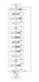
次に、基板処理装置100による成膜処理について、図3を用いて説明する。図3は、本実施形態に係る基板処理装置100における成膜処理の一例を示すフローチャートである。<Deposition process>
Next, film formation processing by the
ステップS101において、基板処理装置100の処理容器1内に基板Wを搬入する。具体的には、ヒータ21により所定温度(例えば、300℃~700℃)に加熱された基板載置台2を搬送位置(図1において二点鎖線で示す。)に下降させた状態でゲートバルブ12を開く。続いて、搬送アーム(図示せず)により基板Wを、搬入出口11を介して処理容器1内に搬入し、基板支持ピン27で支持する。搬送アームが搬入出口11から退避すると、ゲートバルブ12を閉じる。また、基板支持ピン27を下降させて、基板Wを基板載置台2に載置する。 In step S<b>101 , substrates W are loaded into the
ステップS102において、制御装置6は、昇降機構24を制御して、基板載置台(ステージ)2を処理位置(第1処理位置、または、第2処理位置)まで上昇させる。これにより、処理容器1の内部は、処理空間37を含む基板載置台2の表面(基板載置面)側の上部空間と、基板載置台2の裏面側の下部空間と、に区画される。 In step S102, the
ステップS103において、基板載置台2上の基板Wを昇温するとともに、APCバルブ42の開度を調整する。即ち、基板載置台2上の基板Wは、ヒータ21によって所定の温度に昇温される。また、制御装置6は、排気部4を制御して処理容器1内を所定の真空度に調節する。その後、制御装置6は、開閉弁V3,V4を開き、開閉弁V1,V2,V5,V6を閉じる。これにより、N2ガス供給源GS3,GS4から第1の連続N2ガス供給ラインL3及び第2の連続N2ガス供給ラインL4を経てN2ガスを処理空間37内に供給して圧力を上昇させる。また、制御装置6は、処理空間37内の圧力を検出する圧力センサ(図示せず)に基づいて、処理空間37内の圧力が所望の圧力となるAPCバルブ42の開度を調整する。これにより、制御装置6は、処理空間37内の圧力とAPCバルブ42の開度とを対応付けして記憶する。なお、このとき、バッファタンクT1内には、原料ガス供給源GS1からTiCl4ガスが供給されて、バッファタンクT1内の圧力は略一定に維持されている。また、バッファタンクT5,T6内には、N2ガス供給源GS5,GS6からN2ガスが供給されて、バッファタンクT5,T6内の圧力は略一定に維持されている。In step S103, the temperature of the substrate W on the substrate mounting table 2 is raised, and the opening degree of the
ステップS104において、基板WにTiN膜を成膜する基板処理を実行する。なお、ここでの処理は、図4を用いて後述する。基板処理が終了すると、ステップS105に進む。 In step S104, substrate processing for forming a TiN film on the substrate W is performed. Note that the processing here will be described later with reference to FIG. After finishing the substrate processing, the process proceeds to step S105.
ステップS105において、制御装置6は、昇降機構24を制御して、基板載置台(ステージ)2を搬送位置まで下降させる。 In step S105, the
ステップS106において、基板処理装置100の処理容器1内から基板Wを搬出する。具体的には、基板支持ピン27を上昇させて、基板Wを基板載置台2に載置された基板Wを持ち上げ、基板支持ピン27で支持する。また、ゲートバルブ12を開く。続いて、搬送アーム(図示せず)により基板Wを、搬入出口11を介して処理容器1内から搬出する。搬送アームが搬入出口11から退避すると、ゲートバルブ12を閉じる。以上により、基板処理装置100において基板WにTiN膜を成膜する処理が終了する。 In step S<b>106 , the substrate W is unloaded from the
次に、ステップS104の基板処理について、図4から図7を用いて更に説明する。図4は、本実施形態に係る基板処理装置100における基板処理方法の一例を示すフローチャートである。図5は、ガス供給、ギャップ幅、APC開度の制御の一例を説明するタイムチャートである。図6は、1サイクルにおける圧力変動の一例である。図7は、基板処理におけるモデル図の一例である。 Next, the substrate processing in step S104 will be further described with reference to FIGS. 4 to 7. FIG. FIG. 4 is a flow chart showing an example of a substrate processing method in the
なお、図5の上段は、ガス供給を示し、縦軸は供給されるガスの流量、横軸は時間を示す。図5の中段は、基板載置台2の高さ方向の位置を示し、縦軸は基板載置台2の高さ、横軸は時間を示す。即ち、図5の中段のグラフにおいて、縦軸の値が大きいほどギャップ幅が狭く、縦軸の値が小さいほどギャップ幅が広いことを示す。図5の下段は、APCバルブ42の開度を示し、縦軸はAPCバルブ42の開度、横軸は時間を示す。また、図6は、縦軸は圧力、横軸は時間を示す。また、図7は、基板Wの構造体200の一例として、高アスペクト比のホールや溝を示す。なお、構造体200は、上下方向に延びる縦溝と、縦溝から横方向に延びる横溝と、を有するあばら形状の立体構造に適用してもよい。 The upper part of FIG. 5 shows gas supply, the vertical axis represents the flow rate of the supplied gas, and the horizontal axis represents time. The middle part of FIG. 5 indicates the position of the substrate mounting table 2 in the height direction, the vertical axis indicates the height of the substrate mounting table 2, and the horizontal axis indicates time. That is, in the middle graph of FIG. 5, the larger the value on the vertical axis, the narrower the gap width, and the smaller the value on the vertical axis, the wider the gap width. The lower part of FIG. 5 shows the opening degree of the
ステップS1において、制御装置6は、昇降機構24を制御して基板載置台2を第1処理位置(図1参照。図5において、Narrowで示す。)へと移動(上昇)させる上昇動作を開始するとともに、APCバルブ42の開度を第1の開度(図5において、closeで示す。)とする閉じ動作を開始する。ここで第1の開度は、後述する第2の開度よりも小さい(閉じ側)開度である。なお、第1の開度の値は、レシピに記載の圧力と、ステップS103で記憶した圧力と開度との関係と、に基づいて決定される。また、制御装置6は、マスフローコントローラM3,M4の流量(図5において、c-N2で示すキャリアN2ガスの流量)をレシピに設定された所定の流量とする。なお、キャリアN2ガスは、N2ガス供給源GS3,GS4から第1の連続N2ガス供給ラインL3及び第2の連続N2ガス供給ラインL4を経て処理空間37内に供給されている。In step S1, the
ステップS2において、制御装置6は、開閉弁V1を開き、処理空間37内に原料ガスであるTiCl4ガスを供給する。ここで、環状隙間38のギャップ幅G1はギャップ幅G2よりも狭く(例えば、0.5mm)なっており、また、APCバルブ42の開度(第1の開度)も後述する第2の開度よりも小さくなっている。このため、処理空間37内に供給されたTiCl4ガスは処理空間37内に封じ込められ、図6に示すように、処理空間37内の圧力が上昇する。これにより、供給されたTiCl4ガスがすぐに排気されることなく、原料ガス分子と基板Wの構造体200との接触頻度を増加させることができる。また、図7(a)に示すように、複雑な構造体200の奥まで原料ガスを供給することができ、原料ガス分子を構造体200の表面に吸着させることができる。In step S<b>2 , the
ステップS3において、制御装置6は、開閉弁V1を閉じる。また、制御装置6は、昇降機構24を制御して基板載置台2を第2処理位置(図2参照。図5において、Wideで示す。)へと移動(下降)させる下降動作を開始するとともに、APCバルブ42の開度を第2の開度(図5において、Openで示す。)とする開き動作を開始する。ここで第2の開度は、第1の開度よりも大きい(開き側)開度である。なお、第2の開度の値は、レシピに記載の圧力と、ステップS103で記憶した圧力と開度との関係と、に基づいて決定される。 In step S3, the
ステップS4において、制御装置6は、開閉弁V5,V6を開き、処理空間37内にN2ガス(図5において、Flash N2で示す。)を供給する。このとき、N2ガスは、バッファタンクT5,T6に一旦貯留された後に処理容器1内に供給されるので、比較的大きい流量を供給することができる。また、環状隙間38のギャップ幅はギャップ幅G1よりも広くなっており、また、APCバルブ42の開度も第1の開度よりも大きくなっている。これにより、図7(b)に示すように、処理空間37の余剰のTiCl4ガス等をフラッシュパージする。なお、図5において、フラッシュパージは、基板載置台2の下降動作中、APCバルブ42の開度の開き動作中に開始するものとして図示しているが、これに限られるものではなく、基板載置台2の下降動作が終了した後、APCバルブ42の開度調整が完了した後に行ってもよい。In step S4, the
ステップS5において、制御装置6は、開閉弁V5,V6を閉じる。また、制御装置6は、マスフローコントローラM3,M4の流量(キャリアN2ガスの流量)を原料ガス供給時(ステップS2)、フラッシュパージ時(ステップS4)よりも小さくする。また、環状隙間38のギャップ幅G2はギャップ幅G1よりも広く(例えば、6mm)なっており、また、APCバルブ42の開度(第2の開度)も第1の開度よりも大きくなっている。このため、処理空間37から真空ポンプ44への排気コンダクタンスが小さくすることができ、図6に示すように、処理空間37内の圧力が低圧(図6において、low pressureで示す。)となる。これにより、図7(b)に示すように、構造体200内の余剰のTiCl4ガス、N2ガス等を容易に排出することができる。In step S5, the
ステップS6において、制御装置6は、昇降機構24を制御して基板載置台2を第1処理位置(図1参照)へと移動(上昇)させる上昇動作を開始する。 In step S6, the
ステップS7において、制御装置6は、APCバルブ42の開度を第1の開度とする閉じ動作を開始する。また、制御装置6は、マスフローコントローラM3,M4の流量(キャリアN2ガスの流量)をステップS5,6における流量よりも大きくする。例えば、ステップS1~S4の流量に戻す。In step S7, the
ステップS8において、制御装置6は、開閉弁V2を開き、処理空間37内に反応ガスであるNH3ガスを供給する。ここで、環状隙間38のギャップ幅G1はギャップ幅G2よりも狭く(例えば、0.5mm)なっており、また、APCバルブ42の開度(第1の開度)も第2の開度よりも小さくなっている。このため、処理空間37内に供給されたNH3ガスは処理空間37内に封じ込められ、図6に示すように、処理空間37内の圧力が上昇する。これにより、供給されたNH3ガスがすぐに排気されることなく、反応ガス分子と基板Wの構造体200との接触頻度を増加させることができる。また、図7(c)に示すように、複雑な構造体200の奥まで反応ガスを供給することができ、構造体200の表面に吸着された原料ガス分子と反応させることができる。In step S<b>8 , the
ステップS9において、制御装置6は、APCバルブ42の開度を第2の開度とする開き動作を開始する。 In step S9, the
ステップS10において、制御装置6は、開閉弁V2を閉じる。また、昇降機構24を制御して基板載置台2を第2処理位置(図2参照)へと移動(下降)させる下降動作を開始する。 In step S10, the
ステップS11において、制御装置6は、開閉弁V5,V6を開き、処理空間37内にN2ガス(図5において、Flash N2で示す。)を供給する。このとき、N2ガスは、バッファタンクT5,T6に一旦貯留された後に処理容器1内に供給されるので、比較的大きい流量を供給することができる。また、環状隙間38のギャップ幅はギャップ幅G1よりも広くなっており、また、APCバルブ42の開度(第2の開度)も第1の開度よりも大きくなっている。これにより、図7(d)に示すように、処理空間37の反応生成物(NH4Clガス、HClガス)や余剰のNH3ガス等をフラッシュパージする。なお、図5において、フラッシュパージは、APCバルブ42の開度の開き動作終了後、基板載置台2の下降動作中に開始するものとして図示しているが、これに限られるものではない。In step S11, the
ステップS12において、制御装置6は、開閉弁V5,V6を閉じる。また、制御装置6は、マスフローコントローラM3,M4の流量(キャリアN2ガスの流量)を反応ガス供給時(ステップS8,9)、フラッシュパージ時(ステップS11)よりも小さくする。また、環状隙間38のギャップ幅G2はギャップ幅G1よりも広く(例えば、6mm)なっており、また、APCバルブ42の開度(第2の開度)も第1の開度よりも大きくなっている。このため、処理空間37から真空ポンプ44への排気コンダクタンスが小さくすることができ、図6に示すように、処理空間37内の圧力が低圧(図6において、low pressureで示す。)となる。これにより、図7(d)に示すように、構造体200内の反応生成物(NH4Clガス、HClガス)、余剰のNH3ガス、N2ガス等を容易に排出することができる。In step S12, the
ステップS13において、制御装置6は、昇降機構24を制御して基板載置台2を第1処理位置(図1参照)へと移動(上昇)させる上昇動作を開始する。このようなステップS1~S13の処理により、ALDプロセスの1サイクルが終了する。 In step S13, the
ステップS14において、制御装置6は、所定のサイクル数が終了したか否かを判定する。所定のサイクル数が終了していない場合(S14・No)、終了するまでステップS1~S13を繰り返す。所定のサイクル数が終了した場合(S14・Yes)、処理を終了する。 In step S14, the
なお、図5に示す例においては、キャリアN2ガスを連続的に供給する、具体的には、低圧工程時(S5,S6,S12,S13)において、キャリアN2ガスの供給量を低減するものとして説明したが、これに限られるものではない。図8は、ガス供給、ギャップ幅、APC開度の制御の他の一例を説明するタイムチャートである。例えば、図8に示す他の一例のように、キャリアN2ガスを連続的に供給する、具体的には、キャリアN2ガスを一定で供給する構成であってもよい。換言すれば、低圧工程(S5,S6,S12,S13)におけるキャリアN2ガスの供給量は、吸着工程(S2)及び/又は反応工程(S8,S9)におけるキャリアN2ガスの供給量と同じであってもよい。図8に示す他の一例では、APC開度を制御することにより、低圧工程において、処理空間37内の圧力を低圧とする。In the example shown inFIG . 5, the carrierN2 gas is continuously supplied. However, it is not limited to this. FIG. 8 is a time chart illustrating another example of control of gas supply, gap width, and APC opening. For example, as in another example shown in FIG. 8, the carrierN2 gas may be continuously supplied, specifically, the carrierN2 gas may be constantly supplied. In other words, the amount of carrierN2 gas supplied in the low-pressure steps (S5, S6, S12, S13) is the same as the amount of carrierN2 gas supplied in the adsorption step (S2) and/or the reaction steps (S8, S9). may be In another example shown in FIG. 8, the pressure in the
また、環状隙間38のギャップ幅の制御(基板載置台2の昇降)及びAPCバルブ42の開度調整の両方を行うものとして説明したが、これに限られるものではない。例えば、いずれか一方であってもよい。 Also, although the gap width of the
図9(a)は、原料ガスの供給量とステップカバレッジとの関係を示すグラフの一例である。縦軸はステップカバレッジを示し、横軸は原料ガスの供給量を示す。図9(a)に示すように、原料ガスの供給量が増加するほど、ステップカバレッジも向上する。これに対し、本実施形態に係る基板処理装置100によれば、吸着工程における環状隙間38のギャップ幅を小さく、APCバルブ42の開度を小さくすることにより、原料ガスの分圧を上げることができる。原料ガスの分圧を上げることで、処理空間37内の原料ガスの量を増やすことができる。これにより、図9(a)に示すように、ステップカバレッジを向上させることができる。 FIG. 9A is an example of a graph showing the relationship between the supply amount of source gas and step coverage. The vertical axis indicates the step coverage, and the horizontal axis indicates the supply amount of the raw material gas. As shown in FIG. 9A, the step coverage is improved as the supply amount of the raw material gas is increased. In contrast, according to the
図9(b)は、低圧工程時(ステップS5,S6,S12,S13)の圧力とステップカバレッジとの関係を示すグラフの一例である。縦軸はステップカバレッジを示し、横軸は圧力(右を0Torrとし、左に進むほど圧力が大きくなる)を示す。図9(b)に示すように、低圧工程時の圧力が低下するほど、ステップカバレッジも向上する。例えば、原料ガスをパージする工程において、未反応の原料ガスが構造体200内の入り口付近に留まっている場合、構造体200の入口側での成膜が奥側よりも先に進行し、構造体200を閉塞する。このため、ステップカバレッジが低下する。また、反応ガスのパージ時も同様である。本実施形態に係る基板処理装置100によれば、パージ工程における環状隙間38のギャップ幅を大きく、APCバルブ42の開度を大きくすることにより、コンダクタンスを低下させ、圧力を低下させることができる。また、キャリアN2ガスの供給量を低減することにより、圧力を低下させることができる。これにより、図9(b)に示すように、ステップカバレッジを向上させることができる。FIG. 9B is an example of a graph showing the relationship between pressure and step coverage during the low pressure process (steps S5, S6, S12, S13). The vertical axis indicates the step coverage, and the horizontal axis indicates the pressure (0 Torr on the right and the pressure increases toward the left). As shown in FIG. 9B, the lower the pressure in the low-pressure process, the better the step coverage. For example, in the process of purging the raw material gas, if the unreacted raw material gas remains near the entrance of the
図10は、ギャップ距離と膜厚との関係を示すグラフの一例である。ここでは、ギャップ幅を固定して所定のサイクルで成膜を行った。結果を黒塗り四角印(リファレンス)で示す。図10に示すように、ギャップ幅が狭い領域(0.5mm~2mm)において、膜厚が増加することが確認できた。即ち、本実施形態に係る基板処理装置100によれば、原料ガスを溜め込むことにより、原料ガスの使用効率を改善することができる。 FIG. 10 is an example of a graph showing the relationship between gap distance and film thickness. Here, film formation was performed in a predetermined cycle with a fixed gap width. The results are indicated by filled squares (reference). As shown in FIG. 10, it was confirmed that the film thickness increased in the region where the gap width was narrow (0.5 mm to 2 mm). That is, according to the
なお、ギャップ幅0.5mm及び6.0mmについて、黒塗り四角印で示すリファレンスのパージ時間(ステップS3,S10に対応するN2パージ0.1秒、ステップS4,S11に対応するフラッシュパージ0.2秒)よりもパージ時間を延ばした場合を、黒塗り丸印(N2パージ0.4秒、フラッシュパージ0.5秒)、白塗り丸印(N2パージ0.7秒、フラッシュパージ0.8秒)で示す。仮に、ギャップ幅が狭い領域において原料ガスのパージ不足が発生し、ギャップ幅が広い領域において原料ガスのパージ不足が発生していないことに起因して、ギャップ幅が狭い領域において膜厚増加が発生しているとするならば、パージ時間を延ばした場合、ギャップ幅が狭い領域においては大きく膜厚が減少し、ギャップ幅が広い領域においては膜厚の減少が小さくなると考えられる。しかしながら、図10に示すように、ギャップ幅0.5mm及び6.0mmにおいて、同様の膜厚の減少傾向を示している。即ち、ギャップ幅が狭い領域における膜厚増加は原料ガスのパージ不足に起因するものではないことが確認できた。換言すれば、原料ガスの使用効率が改善することが確認できた。For gap widths of 0.5 mm and 6.0 mm, reference purge times indicated by black squares (N2 purge 0.1 sec corresponding to steps S3 and S10, flash purge 0.1 sec corresponding to steps S4 and S11) 2 seconds), black circles (N2 purge 0.4 seconds, flash purge 0.5 seconds), white circles (N2 purge 0.7 seconds, flash purge 0.7 seconds). 8 seconds). If insufficient purging of the raw material gas occurs in the region where the gap width is narrow and insufficient purging of the raw material gas does not occur in the region where the gap width is wide, the film thickness increases in the region where the gap width is narrow. If the purge time is extended, the film thickness will decrease significantly in the region where the gap width is narrow, and the decrease in film thickness will be small in the region where the gap width is wide. However, as shown in FIG. 10, the film thickness tends to decrease similarly at gap widths of 0.5 mm and 6.0 mm. That is, it was confirmed that the increase in the film thickness in the region where the gap width was narrow was not caused by insufficient purging of the raw material gas. In other words, it was confirmed that the usage efficiency of the raw material gas was improved.
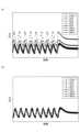
図11は、各ギャップ幅における圧力変化を示すグラフの一例である。ここでは、環状隙間38のギャップ幅をそれぞれの値に固定して、処理空間37へのガスの供給と排気を繰り返した際の圧力変化を示す。縦軸は圧力を示し、横軸は時間を示す。また、図11(a)は処理空間37内の圧力変化を示し、図11(b)は排気ダクト13内の圧力変化を示す。 FIG. 11 is an example of a graph showing pressure change at each gap width. Here, the gap width of the
図11(a)に示す構成の例においては、ギャップ幅が2mm以下の領域では、ギャップ幅の変更により圧力が上昇する、即ち、原料ガスの溜め込みが行われることが確認できた。一方、ギャップ幅が3mm以上の領域では、ギャップ幅の変更による圧力の上昇はほとんど見られなかった。このように、第1処理位置は、図11(a)に示す圧力変動に基づいて、原料ガスの溜め込みが行われる位置、換言すれば、ギャップ幅の変更により圧力が上昇する位置(例えば、ギャップ幅0.5mmとなる位置)に設定される。また、第2処理位置は、図11(a)に示す圧力変動に基づいて、原料ガスの溜め込みが行われていない位置、換言すれば、ギャップ幅の変更により圧力の上昇が小さい位置(例えば、ギャップ幅6.0mmとなる位置)に設定される。また、図11(b)に示すように、排気ダクト13内の圧力はギャップ幅に依らず、ほとんど変化はみられなかった。 In the configuration example shown in FIG. 11A, it was confirmed that, in the region where the gap width is 2 mm or less, the change in the gap width causes the pressure to rise, that is, the raw material gas is accumulated. On the other hand, in the region where the gap width was 3 mm or more, almost no increase in pressure was observed due to the change in gap width. Thus, the first processing position is the position where the raw material gas is accumulated based on the pressure fluctuation shown in FIG. position where the width is 0.5 mm). The second processing position is a position where the raw material gas is not accumulated based on the pressure fluctuation shown in FIG. position where the gap width is 6.0 mm). Moreover, as shown in FIG. 11(b), the pressure in the
以上、本実施形態に係る基板処理装置100によれば、基板Wに成膜する際のステップカバレッジを向上させることができる。 As described above, according to the
また、吸着工程(S2)及び/又は反応工程(S8,S9)におけるギャップ幅を狭くする(2.0mm以下)ことにより、原料ガス及び/又は反応ガスの溜め込みが行われ、原料ガス及び/又は反応ガスの使用効率を改善することができる。また、ステップカバレッジも向上する。また、原料ガス又は反応ガスをパージする工程(S4~S6,S11~S13)におけるギャップ幅を広くする(3.0mm以上)ことにより、原料ガス又は反応ガスを好適にパージすることができる。また、ステップカバレッジも向上する。 In addition, by narrowing the gap width (2.0 mm or less) in the adsorption step (S2) and/or the reaction steps (S8, S9), the raw material gas and/or the reaction gas are accumulated, and the raw material gas and/or It is possible to improve the usage efficiency of the reaction gas. Also, step coverage is improved. Further, by widening the gap width (3.0 mm or more) in the steps of purging the source gas or reaction gas (S4 to S6, S11 to S13), the source gas or reaction gas can be preferably purged. Also, step coverage is improved.
以上、基板処理装置100による本実施形態の成膜方法について説明したが、本開示は上記実施形態等に限定されるものではなく、特許請求の範囲に記載された本開示の要旨の範囲内において、種々の変形、改良が可能である。 As described above, the film forming method of the present embodiment by the
TiN膜を成膜する場合を例に説明したが、成膜する膜の種類はこれに限定されるものではない。また、原料ガス、反応ガス等のガス種も上述したものに限定されるものではない。 Although the case of forming a TiN film has been described as an example, the type of film to be formed is not limited to this. Also, the types of gas such as source gas and reaction gas are not limited to those described above.
また、本実施形態に係る基板処理装置100は、熱ALD装置の場合を例に説明したが、これに限られるものではなく、例えば、プラズマALD装置に適用してもよい。 Further, although the
W 基板
1 処理容器
2 基板載置台(載置台)
3 シャワーヘッド(部材)
4 排気部
5 処理ガス供給機構(原料ガス供給部、反応ガス供給部、キャリアガス供給部)
6 制御装置
22 カバー部材
24 昇降機構
32 シャワープレート(部材)
34 環状突起部(環状凸部)
37 処理空間
38 環状隙間
41 排気配管
42 APCバルブ
43 開閉バルブ
44 真空ポンプ
100 基板処理装置
L1 原料ガス供給ライン(原料ガス供給部)
L2 反応ガス供給ライン(反応ガス供給部)
L3 第1の連続N2ガス供給ライン(キャリアガス供給部)
L4 第2の連続N2ガス供給ライン(キャリアガス供給部)
L5 第1のフラッシュパージライン
L6 第2のフラッシュパージライン
3 shower head (component)
4
6
34 annular protrusion (annular protrusion)
37
L2 reaction gas supply line (reaction gas supply unit)
L3 first continuousN2 gas supply line (carrier gas supply section)
L4 second continuousN2 gas supply line (carrier gas supply section)
L5 First flash purge line L6 Second flash purge line
Claims (9)
Translated fromJapanese前記載置台との間に処理空間を形成する部材と、
前記処理容器内へ原料ガスを供給する原料ガス供給部と、
前記処理容器内へ反応ガスを供給する反応ガス供給部と、
開度調整可能な圧力調整弁を有し、前記処理容器内のガスを排気する排気部と、を備える基板処理装置の基板処理方法であって、
前記処理容器内に原料ガスを供給して前記基板に吸着させる吸着工程と、
前記吸着工程の余剰な原料ガスを排気する第1パージ工程と、
前記処理容器内に反応ガスを供給して前記原料ガスと反応させる反応工程と、
前記反応工程の余剰な反応ガスを排気する第2パージ工程と、を繰り返す工程と、を有し、
前記吸着工程及び/又は前記反応工程における前記載置台と前記部材との間の隙間の幅及び/又は前記圧力調整弁の開度は、前記第1パージ工程及び/又は前記第2パージ工程における前記載置台と前記部材との間の隙間の幅及び/又は前記圧力調整弁の開度よりも小さく、
前記第1パージ工程及び/又は前記第2パージ工程は、
前記処理空間内の圧力を前記吸着工程及び/又は前記反応工程よりも低圧にする低圧工程を有し、
パージガスの供給及び該パージガスの停止後に、前記低圧工程が実施される、
基板処理方法。a processing container having an elevable mounting table on which the substrate is mounted;
a member that forms a processing space between itself and the mounting table;
a raw material gas supply unit for supplying a raw material gas into the processing container;
a reactive gas supply unit that supplies a reactive gas into the processing container;
A substrate processing method for a substrate processing apparatus, comprising: an exhaust unit for exhausting gas in the processing container, the exhaust unit having a pressure control valve whose opening degree can be adjusted;
an adsorption step of supplying a raw material gas into the processing container and adsorbing it onto the substrate;
a first purge step of exhausting excess raw material gas from the adsorption step;
a reaction step of supplying a reaction gas into the processing container and reacting it with the raw material gas;
a step of repeating a second purge step of exhausting excess reaction gas in the reaction step;
The width of the gap between the mounting table and the member and/or the opening degree of the pressure regulating valve in the adsorption step and/or the reaction step are set before the first purge step and/or the second purge step.smaller than the width of the gap between the mounting table and the member and/or the opening of the pressure regulating valve,
The first purging step and/or the second purging step,
a low-pressure step in which the pressure in the treatment space is lower than that in the adsorption step and/or the reaction step;
The low-pressure step is performed after the purge gas is supplied and the purge gas is stopped.
Substrate processing method.
キャリアガスを供給するキャリアガス供給部を更に備え、
前記吸着工程、前記第1パージ工程、前記反応工程、前記第2パージ工程において、キャリアガスを連続的に供給する、
請求項1に記載の基板処理方法。The substrate processing apparatus is
further comprising a carrier gas supply unit for supplying a carrier gas,
continuously supplying a carrier gas in the adsorption step, the first purge step, the reaction step, and the second purge step;
The substrate processing method according to claim1 .
請求項2に記載の基板処理方法。The supply amount of the carrier gas in the low-pressure step is smaller than the supply amount of the carrier gas in the adsorption step and/or the reaction step,
The substrate processing method according to claim2 .
請求項2に記載の基板処理方法。The supply amount of the carrier gas in the low-pressure step is the same as the supply amount of the carrier gas in the adsorption step and/or the reaction step.
The substrate processing method according to claim2 .
請求項1乃至請求項4のいずれか1項に記載の基板処理方法。The width of the gap between the mounting table and the member is controlled by moving the mounting table up and down.
The substrate processing method according to any one of claims 1 to4 .
請求項1乃至請求項5のいずれか1項に記載の基板処理方法。The member is a shower plate facing the mounting table,
The substrate processing method according to any one of claims 1 to5 .
前記載置台は、その周縁部にカバー部材を有し、
前記環状凸部の下面と前記カバー部材の上面との幅を制御する、
請求項6に記載の基板処理方法。The shower plate has an annular protrusion on its peripheral edge,
The mounting table has a cover member on its peripheral edge,
controlling the width between the lower surface of the annular protrusion and the upper surface of the cover member;
The substrate processing method according to claim6 .
請求項1乃至請求項7のいずれか1項に記載の基板処理方法。The width of the gap between the mounting table and the member in the adsorption step and/or the reaction step is 2.0 mm or less.
The substrate processing method according to any one of claims 1 to7 .
前記載置台の載置面に対向して配置され、前記載置台との間に処理空間を形成する部材と、
前記処理容器内へ原料ガスを供給する原料ガス供給部と、
前記処理容器内へ反応ガスを供給する反応ガス供給部と、
開度調整可能な圧力調整弁を有し、前記処理容器内のガスを排気する排気部と、
制御部と、を備え、
前記制御部は、
前記処理容器内に原料ガスを供給して前記基板に吸着させる吸着工程と、
前記吸着工程の余剰な原料ガスを排気する第1パージ工程と、
前記処理容器内に反応ガスを供給して前記原料ガスと反応させる反応工程と、
前記反応工程の余剰な反応ガスを排気する第2パージ工程と、を繰り返す工程と、を実行し、
前記吸着工程及び/又は前記反応工程における前記載置台と前記部材との間の隙間の幅及び/又は前記圧力調整弁の開度は、前記第1パージ工程及び/又は前記第2パージ工程における前記載置台と前記部材との間の隙間の幅及び/又は前記圧力調整弁の開度よりも小さくなるように制御し、
前記第1パージ工程及び/又は前記第2パージ工程は、
前記処理空間内の圧力を前記吸着工程及び/又は前記反応工程よりも低圧にする低圧工程を有し、
パージガスの供給及び該パージガスの停止後に、前記低圧工程が実施される、
基板処理装置。
a processing container having an elevable mounting table on which the substrate is mounted;
a member arranged to face the mounting surface of the mounting table and forming a processing space between itself and the mounting table;
a raw material gas supply unit for supplying a raw material gas into the processing container;
a reactive gas supply unit that supplies a reactive gas into the processing container;
an exhaust unit having a pressure control valve whose degree of opening is adjustable and for exhausting gas in the processing container;
a control unit;
The control unit
an adsorption step of supplying a raw material gas into the processing container and adsorbing it onto the substrate;
a first purge step of exhausting excess raw material gas from the adsorption step;
a reaction step of supplying a reaction gas into the processing container and reacting it with the raw material gas;
performing a step of repeating a second purge step of exhausting excess reaction gas in the reaction step;
The width of the gap between the mounting table and the member and/or the opening degree of the pressure regulating valve in the adsorption step and/or the reaction step are set before the first purge step and/or the second purge step. controlling to be smaller than the width of the gap between the mounting table and the member and/or the opening of the pressure regulating valve;
The first purging step and/or the second purging step,
a low-pressure step in which the pressure in the treatment space is lower than that in the adsorption step and/or the reaction step;
The low-pressure step is performed after the purge gas is supplied and the purge gas is stopped.
Substrate processing equipment.
Priority Applications (5)
| Application Number | Priority Date | Filing Date | Title |
|---|---|---|---|
| JP2019108977AJP7300898B2 (en) | 2019-06-11 | 2019-06-11 | Substrate processing method and substrate processing apparatus |
| TW109118414ATW202111774A (en) | 2019-06-11 | 2020-06-02 | Substrate processing method and substrate processing apparatus |
| US16/892,766US11732357B2 (en) | 2019-06-11 | 2020-06-04 | Substrate processing method and substrate processing apparatus |
| KR1020200067583AKR102392368B1 (en) | 2019-06-11 | 2020-06-04 | Substrate processing method and substrate processing apparatus |
| CN202010500322.8ACN112071752B (en) | 2019-06-11 | 2020-06-04 | Substrate processing method and substrate processing apparatus |
Applications Claiming Priority (1)
| Application Number | Priority Date | Filing Date | Title |
|---|---|---|---|
| JP2019108977AJP7300898B2 (en) | 2019-06-11 | 2019-06-11 | Substrate processing method and substrate processing apparatus |
Publications (2)
| Publication Number | Publication Date |
|---|---|
| JP2020200510A JP2020200510A (en) | 2020-12-17 |
| JP7300898B2true JP7300898B2 (en) | 2023-06-30 |
Family
ID=73656445
Family Applications (1)
| Application Number | Title | Priority Date | Filing Date |
|---|---|---|---|
| JP2019108977AActiveJP7300898B2 (en) | 2019-06-11 | 2019-06-11 | Substrate processing method and substrate processing apparatus |
Country Status (5)
| Country | Link |
|---|---|
| US (1) | US11732357B2 (en) |
| JP (1) | JP7300898B2 (en) |
| KR (1) | KR102392368B1 (en) |
| CN (1) | CN112071752B (en) |
| TW (1) | TW202111774A (en) |
Families Citing this family (5)
| Publication number | Priority date | Publication date | Assignee | Title |
|---|---|---|---|---|
| JP7300898B2 (en)* | 2019-06-11 | 2023-06-30 | 東京エレクトロン株式会社 | Substrate processing method and substrate processing apparatus |
| US11236424B2 (en)* | 2019-11-01 | 2022-02-01 | Applied Materials, Inc. | Process kit for improving edge film thickness uniformity on a substrate |
| US20230072156A1 (en)* | 2021-09-02 | 2023-03-09 | Wonik Ips Co., Ltd. | Substrate processing apparatus |
| JP2024002304A (en) | 2022-06-23 | 2024-01-11 | 東京エレクトロン株式会社 | Film deposition apparatus |
| CN119194414B (en)* | 2024-11-06 | 2025-07-11 | 南京原磊纳米材料有限公司 | Atomic layer deposition coating method and system for high aspect ratio structural devices |
Citations (4)
| Publication number | Priority date | Publication date | Assignee | Title |
|---|---|---|---|---|
| JP2006283172A (en) | 2005-04-04 | 2006-10-19 | Smc Corp | Deposition operation method with ALD compatible vacuum flow control valve |
| JP2011060936A (en) | 2009-09-09 | 2011-03-24 | Hitachi Kokusai Electric Inc | Method of manufacturing semiconductor device, and substrate processing apparatus |
| JP2017005016A (en) | 2015-06-05 | 2017-01-05 | 株式会社日立国際電気 | Semiconductor device manufacturing method, substrate processing apparatus and program |
| JP2018150612A (en) | 2017-03-15 | 2018-09-27 | 東京エレクトロン株式会社 | Substrate processing apparatus and substrate processing method |
Family Cites Families (32)
| Publication number | Priority date | Publication date | Assignee | Title |
|---|---|---|---|---|
| JPH0799162A (en)* | 1993-06-21 | 1995-04-11 | Hitachi Ltd | CVD reactor device |
| US6352593B1 (en)* | 1997-08-11 | 2002-03-05 | Torrex Equipment Corp. | Mini-batch process chamber |
| US7393561B2 (en)* | 1997-08-11 | 2008-07-01 | Applied Materials, Inc. | Method and apparatus for layer by layer deposition of thin films |
| KR101416781B1 (en)* | 2003-03-14 | 2014-07-08 | 아익스트론 인코포레이티드 | Methods and apparatus for atomic layer deposition |
| KR100614801B1 (en)* | 2004-07-05 | 2006-08-22 | 삼성전자주식회사 | Film Formation Method of Semiconductor Device |
| KR100871003B1 (en)* | 2004-08-06 | 2008-11-27 | 도쿄엘렉트론가부시키가이샤 | Thin film forming method and thin film forming apparatus |
| US20070116888A1 (en)* | 2005-11-18 | 2007-05-24 | Tokyo Electron Limited | Method and system for performing different deposition processes within a single chamber |
| US7897217B2 (en)* | 2005-11-18 | 2011-03-01 | Tokyo Electron Limited | Method and system for performing plasma enhanced atomic layer deposition |
| US20070235319A1 (en)* | 2006-04-07 | 2007-10-11 | Tokyo Electron Limited | Multi-processing using an ionized physical vapor deposition (ipvd) system |
| KR100829821B1 (en)* | 2006-10-25 | 2008-05-19 | 주식회사 아이피에스 | Thin film deposition method |
| JP5176358B2 (en)* | 2007-03-27 | 2013-04-03 | 東京エレクトロン株式会社 | Film forming apparatus and film forming method |
| CN100590803C (en)* | 2007-06-22 | 2010-02-17 | 中芯国际集成电路制造(上海)有限公司 | Atomic layer deposition method and formed semiconductor device |
| JP5347294B2 (en)* | 2007-09-12 | 2013-11-20 | 東京エレクトロン株式会社 | Film forming apparatus, film forming method, and storage medium |
| JP5544697B2 (en)* | 2008-09-30 | 2014-07-09 | 東京エレクトロン株式会社 | Deposition equipment |
| JP5665289B2 (en)* | 2008-10-29 | 2015-02-04 | 株式会社日立国際電気 | Semiconductor device manufacturing method, substrate processing method, and substrate processing apparatus |
| JP2013040398A (en)* | 2011-07-20 | 2013-02-28 | Tokyo Electron Ltd | Film forming method and film forming apparatus |
| JP6105967B2 (en)* | 2012-03-21 | 2017-03-29 | 株式会社日立国際電気 | Semiconductor device manufacturing method, substrate processing method, substrate processing apparatus, and program |
| JP2014082322A (en)* | 2012-10-16 | 2014-05-08 | Tokyo Electron Ltd | Method for depositing silicon nitride film and deposition device |
| JP5977364B2 (en)* | 2012-11-26 | 2016-08-24 | 株式会社日立国際電気 | Semiconductor device manufacturing method, substrate processing apparatus, and recording medium |
| US9865501B2 (en)* | 2013-03-06 | 2018-01-09 | Lam Research Corporation | Method and apparatus for remote plasma treatment for reducing metal oxides on a metal seed layer |
| JP6245643B2 (en)* | 2013-03-28 | 2017-12-13 | 株式会社日立国際電気 | Semiconductor device manufacturing method, substrate processing apparatus, and program |
| JP6391355B2 (en)* | 2014-08-11 | 2018-09-19 | 東京エレクトロン株式会社 | Method for forming tungsten film |
| CN105839068B (en)* | 2015-01-30 | 2018-09-21 | 东京毅力科创株式会社 | The film build method of tungsten film |
| JP6751631B2 (en)* | 2016-09-13 | 2020-09-09 | 東京エレクトロン株式会社 | How to fill the recesses of the board with tungsten |
| KR102065243B1 (en)* | 2017-05-01 | 2020-01-10 | 도쿄엘렉트론가부시키가이샤 | Film forming method and film forming apparatus |
| JP6691152B2 (en)* | 2018-02-07 | 2020-04-28 | 株式会社Kokusai Electric | Semiconductor device manufacturing method, substrate processing apparatus, and program |
| JP6770988B2 (en)* | 2018-03-14 | 2020-10-21 | 株式会社Kokusai Electric | Manufacturing method for substrate processing equipment and semiconductor equipment |
| JP7296699B2 (en)* | 2018-07-02 | 2023-06-23 | 東京エレクトロン株式会社 | GAS SUPPLY SYSTEM, PLASMA PROCESSING APPARATUS, AND GAS SUPPLY SYSTEM CONTROL METHOD |
| JP7225599B2 (en)* | 2018-08-10 | 2023-02-21 | 東京エレクトロン株式会社 | Deposition equipment |
| JP7134263B2 (en)* | 2019-01-29 | 2022-09-09 | 東京エレクトロン株式会社 | Film forming method, film forming apparatus, and oxidation treatment method |
| JP7175224B2 (en)* | 2019-03-13 | 2022-11-18 | 東京エレクトロン株式会社 | Substrate processing method and substrate processing apparatus |
| JP7300898B2 (en)* | 2019-06-11 | 2023-06-30 | 東京エレクトロン株式会社 | Substrate processing method and substrate processing apparatus |
- 2019
- 2019-06-11JPJP2019108977Apatent/JP7300898B2/enactiveActive
- 2020
- 2020-06-02TWTW109118414Apatent/TW202111774A/enunknown
- 2020-06-04KRKR1020200067583Apatent/KR102392368B1/enactiveActive
- 2020-06-04USUS16/892,766patent/US11732357B2/enactiveActive
- 2020-06-04CNCN202010500322.8Apatent/CN112071752B/enactiveActive
Patent Citations (4)
| Publication number | Priority date | Publication date | Assignee | Title |
|---|---|---|---|---|
| JP2006283172A (en) | 2005-04-04 | 2006-10-19 | Smc Corp | Deposition operation method with ALD compatible vacuum flow control valve |
| JP2011060936A (en) | 2009-09-09 | 2011-03-24 | Hitachi Kokusai Electric Inc | Method of manufacturing semiconductor device, and substrate processing apparatus |
| JP2017005016A (en) | 2015-06-05 | 2017-01-05 | 株式会社日立国際電気 | Semiconductor device manufacturing method, substrate processing apparatus and program |
| JP2018150612A (en) | 2017-03-15 | 2018-09-27 | 東京エレクトロン株式会社 | Substrate processing apparatus and substrate processing method |
Also Published As
| Publication number | Publication date |
|---|---|
| TW202111774A (en) | 2021-03-16 |
| US20200392622A1 (en) | 2020-12-17 |
| CN112071752A (en) | 2020-12-11 |
| KR20200141935A (en) | 2020-12-21 |
| KR102392368B1 (en) | 2022-05-02 |
| CN112071752B (en) | 2024-07-19 |
| JP2020200510A (en) | 2020-12-17 |
| US11732357B2 (en) | 2023-08-22 |
Similar Documents
| Publication | Publication Date | Title |
|---|---|---|
| JP7300898B2 (en) | Substrate processing method and substrate processing apparatus | |
| US9972500B2 (en) | Method of manufacturing semiconductor device | |
| US10870919B2 (en) | Gas supply method and film forming method | |
| US20160351402A1 (en) | Method of reducing stress in metal film and metal film forming method | |
| US20170283945A1 (en) | Substrate Processing Apparatus | |
| US20180112312A1 (en) | Film forming apparatus and film forming method | |
| US9659767B2 (en) | Substrate processing apparatus and method of manufacturing semiconductor device | |
| JP6964473B2 (en) | Gas supply equipment and film formation equipment | |
| US12173401B2 (en) | Method for manufacturing semiconductor device, and film-forming device | |
| JP7149788B2 (en) | Film forming method and film forming apparatus | |
| US12084757B2 (en) | Method of manufacturing semiconductor device, substrate processing apparatus, method of processing substrate, and recording medium | |
| KR20210128914A (en) | Raw material supply apparatus and film forming apparatus | |
| US11028479B2 (en) | Method of forming film | |
| KR102652354B1 (en) | Method of manufacturing semiconductor device, substrate processing apparatus, substrate processing method and program | |
| JP7300913B2 (en) | Substrate processing method and substrate processing apparatus | |
| WO2024018968A1 (en) | Substrate processing method and substrate processing device | |
| US20200056287A1 (en) | Film-Forming Method and Film-Forming Apparatus | |
| JP2020047640A (en) | Substrate processing apparatus, semiconductor device manufacturing method and program | |
| JP2022054653A (en) | Recess embedding method and substrate processing device | |
| JP2020172673A (en) | Substrate treatment apparatus and substrate treatment method |
Legal Events
| Date | Code | Title | Description |
|---|---|---|---|
| A621 | Written request for application examination | Free format text:JAPANESE INTERMEDIATE CODE: A621 Effective date:20220214 | |
| A977 | Report on retrieval | Free format text:JAPANESE INTERMEDIATE CODE: A971007 Effective date:20221214 | |
| A131 | Notification of reasons for refusal | Free format text:JAPANESE INTERMEDIATE CODE: A131 Effective date:20230104 | |
| A521 | Request for written amendment filed | Free format text:JAPANESE INTERMEDIATE CODE: A523 Effective date:20230220 | |
| TRDD | Decision of grant or rejection written | ||
| A01 | Written decision to grant a patent or to grant a registration (utility model) | Free format text:JAPANESE INTERMEDIATE CODE: A01 Effective date:20230523 | |
| A61 | First payment of annual fees (during grant procedure) | Free format text:JAPANESE INTERMEDIATE CODE: A61 Effective date:20230620 | |
| R150 | Certificate of patent or registration of utility model | Ref document number:7300898 Country of ref document:JP Free format text:JAPANESE INTERMEDIATE CODE: R150 |