JP7295089B2 - printed circuit board - Google Patents
printed circuit boardDownload PDFInfo
- Publication number
- JP7295089B2 JP7295089B2JP2020504201AJP2020504201AJP7295089B2JP 7295089 B2JP7295089 B2JP 7295089B2JP 2020504201 AJP2020504201 AJP 2020504201AJP 2020504201 AJP2020504201 AJP 2020504201AJP 7295089 B2JP7295089 B2JP 7295089B2
- Authority
- JP
- Japan
- Prior art keywords
- insulating layer
- circuit pattern
- layer
- outer layer
- circuit board
- Prior art date
- Legal status (The legal status is an assumption and is not a legal conclusion. Google has not performed a legal analysis and makes no representation as to the accuracy of the status listed.)
- Active
Links
Images


Classifications
- H—ELECTRICITY
- H05—ELECTRIC TECHNIQUES NOT OTHERWISE PROVIDED FOR
- H05K—PRINTED CIRCUITS; CASINGS OR CONSTRUCTIONAL DETAILS OF ELECTRIC APPARATUS; MANUFACTURE OF ASSEMBLAGES OF ELECTRICAL COMPONENTS
- H05K1/00—Printed circuits
- H05K1/02—Details
- H05K1/0296—Conductive pattern lay-out details not covered by sub groups H05K1/02 - H05K1/0295
- H05K1/0298—Multilayer circuits
- H—ELECTRICITY
- H05—ELECTRIC TECHNIQUES NOT OTHERWISE PROVIDED FOR
- H05K—PRINTED CIRCUITS; CASINGS OR CONSTRUCTIONAL DETAILS OF ELECTRIC APPARATUS; MANUFACTURE OF ASSEMBLAGES OF ELECTRICAL COMPONENTS
- H05K3/00—Apparatus or processes for manufacturing printed circuits
- H05K3/46—Manufacturing multilayer circuits
- H05K3/4644—Manufacturing multilayer circuits by building the multilayer layer by layer, i.e. build-up multilayer circuits
- H05K3/4682—Manufacture of core-less build-up multilayer circuits on a temporary carrier or on a metal foil
- H—ELECTRICITY
- H05—ELECTRIC TECHNIQUES NOT OTHERWISE PROVIDED FOR
- H05K—PRINTED CIRCUITS; CASINGS OR CONSTRUCTIONAL DETAILS OF ELECTRIC APPARATUS; MANUFACTURE OF ASSEMBLAGES OF ELECTRICAL COMPONENTS
- H05K3/00—Apparatus or processes for manufacturing printed circuits
- H05K3/10—Apparatus or processes for manufacturing printed circuits in which conductive material is applied to the insulating support in such a manner as to form the desired conductive pattern
- H05K3/107—Apparatus or processes for manufacturing printed circuits in which conductive material is applied to the insulating support in such a manner as to form the desired conductive pattern by filling grooves in the support with conductive material
- H—ELECTRICITY
- H05—ELECTRIC TECHNIQUES NOT OTHERWISE PROVIDED FOR
- H05K—PRINTED CIRCUITS; CASINGS OR CONSTRUCTIONAL DETAILS OF ELECTRIC APPARATUS; MANUFACTURE OF ASSEMBLAGES OF ELECTRICAL COMPONENTS
- H05K1/00—Printed circuits
- H05K1/02—Details
- H05K1/03—Use of materials for the substrate
- H05K1/0306—Inorganic insulating substrates, e.g. ceramic, glass
- H—ELECTRICITY
- H05—ELECTRIC TECHNIQUES NOT OTHERWISE PROVIDED FOR
- H05K—PRINTED CIRCUITS; CASINGS OR CONSTRUCTIONAL DETAILS OF ELECTRIC APPARATUS; MANUFACTURE OF ASSEMBLAGES OF ELECTRICAL COMPONENTS
- H05K1/00—Printed circuits
- H05K1/02—Details
- H05K1/03—Use of materials for the substrate
- H05K1/0313—Organic insulating material
- H—ELECTRICITY
- H05—ELECTRIC TECHNIQUES NOT OTHERWISE PROVIDED FOR
- H05K—PRINTED CIRCUITS; CASINGS OR CONSTRUCTIONAL DETAILS OF ELECTRIC APPARATUS; MANUFACTURE OF ASSEMBLAGES OF ELECTRICAL COMPONENTS
- H05K1/00—Printed circuits
- H05K1/02—Details
- H05K1/11—Printed elements for providing electric connections to or between printed circuits
- H05K1/115—Via connections; Lands around holes or via connections
- H—ELECTRICITY
- H05—ELECTRIC TECHNIQUES NOT OTHERWISE PROVIDED FOR
- H05K—PRINTED CIRCUITS; CASINGS OR CONSTRUCTIONAL DETAILS OF ELECTRIC APPARATUS; MANUFACTURE OF ASSEMBLAGES OF ELECTRICAL COMPONENTS
- H05K3/00—Apparatus or processes for manufacturing printed circuits
- H05K3/22—Secondary treatment of printed circuits
- H05K3/28—Applying non-metallic protective coatings
- H—ELECTRICITY
- H05—ELECTRIC TECHNIQUES NOT OTHERWISE PROVIDED FOR
- H05K—PRINTED CIRCUITS; CASINGS OR CONSTRUCTIONAL DETAILS OF ELECTRIC APPARATUS; MANUFACTURE OF ASSEMBLAGES OF ELECTRICAL COMPONENTS
- H05K3/00—Apparatus or processes for manufacturing printed circuits
- H05K3/40—Forming printed elements for providing electric connections to or between printed circuits
- H05K3/42—Plated through-holes or plated via connections
- H05K3/425—Plated through-holes or plated via connections characterised by the sequence of steps for plating the through-holes or via connections in relation to the conductive pattern
- H05K3/428—Plated through-holes or plated via connections characterised by the sequence of steps for plating the through-holes or via connections in relation to the conductive pattern initial plating of through-holes in substrates having a metal pattern
- H—ELECTRICITY
- H05—ELECTRIC TECHNIQUES NOT OTHERWISE PROVIDED FOR
- H05K—PRINTED CIRCUITS; CASINGS OR CONSTRUCTIONAL DETAILS OF ELECTRIC APPARATUS; MANUFACTURE OF ASSEMBLAGES OF ELECTRICAL COMPONENTS
- H05K3/00—Apparatus or processes for manufacturing printed circuits
- H05K3/46—Manufacturing multilayer circuits
- H05K3/4611—Manufacturing multilayer circuits by laminating two or more circuit boards
- H05K3/4623—Manufacturing multilayer circuits by laminating two or more circuit boards the circuit boards having internal via connections between two or more circuit layers before lamination, e.g. double-sided circuit boards
- H—ELECTRICITY
- H05—ELECTRIC TECHNIQUES NOT OTHERWISE PROVIDED FOR
- H05K—PRINTED CIRCUITS; CASINGS OR CONSTRUCTIONAL DETAILS OF ELECTRIC APPARATUS; MANUFACTURE OF ASSEMBLAGES OF ELECTRICAL COMPONENTS
- H05K3/00—Apparatus or processes for manufacturing printed circuits
- H05K3/46—Manufacturing multilayer circuits
- H05K3/4644—Manufacturing multilayer circuits by building the multilayer layer by layer, i.e. build-up multilayer circuits
- H05K3/465—Manufacturing multilayer circuits by building the multilayer layer by layer, i.e. build-up multilayer circuits by applying an insulating layer having channels for the next circuit layer
- H—ELECTRICITY
- H05—ELECTRIC TECHNIQUES NOT OTHERWISE PROVIDED FOR
- H05K—PRINTED CIRCUITS; CASINGS OR CONSTRUCTIONAL DETAILS OF ELECTRIC APPARATUS; MANUFACTURE OF ASSEMBLAGES OF ELECTRICAL COMPONENTS
- H05K2201/00—Indexing scheme relating to printed circuits covered by H05K1/00
- H05K2201/01—Dielectrics
- H05K2201/0183—Dielectric layers
- H05K2201/0195—Dielectric or adhesive layers comprising a plurality of layers, e.g. in a multilayer structure
- H—ELECTRICITY
- H05—ELECTRIC TECHNIQUES NOT OTHERWISE PROVIDED FOR
- H05K—PRINTED CIRCUITS; CASINGS OR CONSTRUCTIONAL DETAILS OF ELECTRIC APPARATUS; MANUFACTURE OF ASSEMBLAGES OF ELECTRICAL COMPONENTS
- H05K2201/00—Indexing scheme relating to printed circuits covered by H05K1/00
- H05K2201/02—Fillers; Particles; Fibers; Reinforcement materials
- H05K2201/0203—Fillers and particles
- H05K2201/0206—Materials
- H05K2201/0209—Inorganic, non-metallic particles
- H—ELECTRICITY
- H05—ELECTRIC TECHNIQUES NOT OTHERWISE PROVIDED FOR
- H05K—PRINTED CIRCUITS; CASINGS OR CONSTRUCTIONAL DETAILS OF ELECTRIC APPARATUS; MANUFACTURE OF ASSEMBLAGES OF ELECTRICAL COMPONENTS
- H05K2201/00—Indexing scheme relating to printed circuits covered by H05K1/00
- H05K2201/03—Conductive materials
- H05K2201/0332—Structure of the conductor
- H05K2201/0364—Conductor shape
- H05K2201/0376—Flush conductors, i.e. flush with the surface of the printed circuit
- H—ELECTRICITY
- H05—ELECTRIC TECHNIQUES NOT OTHERWISE PROVIDED FOR
- H05K—PRINTED CIRCUITS; CASINGS OR CONSTRUCTIONAL DETAILS OF ELECTRIC APPARATUS; MANUFACTURE OF ASSEMBLAGES OF ELECTRICAL COMPONENTS
- H05K2201/00—Indexing scheme relating to printed circuits covered by H05K1/00
- H05K2201/09—Shape and layout
- H05K2201/09209—Shape and layout details of conductors
- H05K2201/095—Conductive through-holes or vias
- H05K2201/09563—Metal filled via
- H—ELECTRICITY
- H05—ELECTRIC TECHNIQUES NOT OTHERWISE PROVIDED FOR
- H05K—PRINTED CIRCUITS; CASINGS OR CONSTRUCTIONAL DETAILS OF ELECTRIC APPARATUS; MANUFACTURE OF ASSEMBLAGES OF ELECTRICAL COMPONENTS
- H05K2201/00—Indexing scheme relating to printed circuits covered by H05K1/00
- H05K2201/09—Shape and layout
- H05K2201/09209—Shape and layout details of conductors
- H05K2201/095—Conductive through-holes or vias
- H05K2201/096—Vertically aligned vias, holes or stacked vias
Landscapes
- Engineering & Computer Science (AREA)
- Microelectronics & Electronic Packaging (AREA)
- Manufacturing & Machinery (AREA)
- Chemical & Material Sciences (AREA)
- Ceramic Engineering (AREA)
- Inorganic Chemistry (AREA)
- Production Of Multi-Layered Print Wiring Board (AREA)
- Structure Of Printed Boards (AREA)
Description
Translated fromJapanese 本発明は、印刷回路基板に関するものであって、特に両面に埋め込まれた回路パターンを含む印刷回路基板およびその製造方法に関する。 BACKGROUND OF THE
印刷回路基板(Printed Circuit Board;PCB)は、所定の電子部品を電気的に連結するか、または機械的に固定する回路基板であって、フェノール樹脂またはエポキシ樹脂などの絶縁層に付着されて、所定の配線パターンが形成される銅箔層で構成される。 2. Description of the Related Art A printed circuit board (PCB) is a circuit board that electrically connects or mechanically fixes predetermined electronic components, and is attached to an insulating layer such as phenol resin or epoxy resin. It is composed of a copper foil layer on which a predetermined wiring pattern is formed.
このような、印刷回路基板は、層数に応じて絶縁層の片面のみに配線が形成された片面印刷回路基板、絶縁層の両面に配線が形成された両面印刷回路基板および多層配線が形成された多層印刷回路基板に大きく分類される。 Such a printed circuit board includes a single-sided printed circuit board in which wiring is formed only on one side of an insulating layer, a double-sided printed circuit board in which wiring is formed on both sides of an insulating layer, and a multi-layered printed circuit board. It is broadly classified as a multi-layer printed circuit board.
このうち、多層印刷回路基板は、製織されたガラス繊維にBTやFR-4、または他の樹脂を含浸させてコアを製造した後、コアの両面に銅箔を積層して内層回路を形成し、その後、サブトラクティブ(Subtractive)工程やセミアディティブ(Semi-additive)工程などを用いて基板を製造する。 Among these, multilayer printed circuit boards are manufactured by impregnating woven glass fiber with BT, FR-4, or other resins to form a core, and then laminating copper foil on both sides of the core to form an inner layer circuit. After that, a substrate is manufactured using a subtractive process, a semi-additive process, or the like.
図1は、従来技術による印刷回路基板の構造を示す図である。 FIG. 1 is a diagram showing the structure of a printed circuit board according to the prior art.
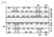
図1を参照すると、従来の印刷回路基板10は、第1絶縁層11、第1回路パターン12、第2絶縁層13、第1ビア14、第2ビア15、第2回路パターン16、第3回路パターン17、第1保護層18および第2保護層19を含む。 Referring to FIG. 1, a conventional
上記のような印刷回路基板10は、第1絶縁層11の両面に第1回路パターン12と第3回路パターン17が配置される。 In the printed
そして、第2絶縁層13は、前記第1絶縁層11上に配置される。また、第2回路パターン16は、前記第2絶縁層13の上面の上に配置される。 A second
そして、第1ビア14は、前記第1絶縁層11を貫通して配置され、それによって前記第1絶縁層11の上面および下面にそれぞれ配置された第1回路パターン12と第3回路パターン17を電気的に連結する。 The
また、第2ビア15は、前記第2絶縁層13を貫通して配置され、それによって前記第1絶縁層11の上面および前記第2絶縁層13の上面にそれぞれ配置された前記第1回路パターン12と前記第2回路パターン16を電気的に連結する。 Also, the
また、第1保護層18は、前記第2絶縁層13の上に配置され、それによって前記第2絶縁層13の上面および前記第2回路パターン16の一部の表面を覆う。 Also, a first
また、前記第2保護層19は、前記第1絶縁層11の下に配置され、それによって前記第1絶縁層11の下面および前記第3回路パターン17の一部の表面を覆う。 Also, the second
しかし、このような従来技術による印刷回路基板は、外層回路パターンに対応する第2回路パターン16および第3回路パターン17が絶縁層の表面上に突出した形態で形成され、これにより前記外層回路パターンに対応する厚さだけ全体の印刷回路基板の厚さが増加するという問題点がある。 However, in the printed circuit board according to the prior art, the
また、従来の印刷回路基板は、外層回路パターンが埋め込みパターンでないので、微細パターンを形成するためには、プライマーのような特殊レジンを使用して回路パターンを形成すべきであるという問題点がある。 In addition, in the conventional printed circuit board, since the outer layer circuit pattern is not an embedded pattern, there is a problem that the circuit pattern should be formed using a special resin such as a primer in order to form a fine pattern. .
また、従来の印刷回路基板は、前記外層回路パターンが突出構造を有するので、基板の最外層に、前記外層回路パターンの表面を保護するためにソルダーレジストのような熱硬化性エポキシを使用して保護層を形成するべきであり、これに伴い製品単価が上昇するという問題点がある。 In addition, in the conventional printed circuit board, since the outer layer circuit pattern has a protruding structure, thermosetting epoxy such as solder resist is used as the outermost layer of the board to protect the surface of the outer layer circuit pattern. A protective layer should be formed, which raises the problem of increasing the unit price of the product.
また、従来の印刷回路基板は、ガラス繊維を有する熱硬化性樹脂を使用して絶縁層を製造するので、各層ごとの導電のためのビアを形成するときに困難がある。 In addition, since the conventional printed circuit board uses a thermosetting resin with glass fibers to manufacture the insulating layers, it is difficult to form vias for conduction in each layer.
本発明による実施例においては、微細パターンの形成が可能でありながら、全体の厚さを減少させることができる印刷回路基板およびその製造方法を提供する。 Embodiments according to the present invention provide a printed circuit board and a method of manufacturing the same, which are capable of forming a fine pattern and reducing the overall thickness.
提案される実施例で解決しようとする技術的課題は、以上で言及した技術的課題に制限されず、言及していないまた他の技術的課題は、下記の記載から提案される実施例が属する技術分野における通常の知識を有する者にとって明確に理解されるであろう。 The technical problems to be solved by the proposed embodiments are not limited to the technical problems mentioned above, and other technical problems not mentioned belong to the proposed embodiments from the following description. It will be clearly understood by those having ordinary knowledge in the technical field.
本発明の実施例に係る印刷回路基板は、第1絶縁層と、前記第1絶縁層の上面の上に配置された内層回路パターンと、前記第1絶縁層の上に配置され、前記内層回路パターンを覆う第2絶縁層と、前記第1絶縁層の下面に形成された複数の第1溝部と、前記複数の第1溝部内に配置される複数の第1外層回路パターンと、前記第2絶縁層の上面に形成された複数の第2溝部と、前記複数の第2溝部内に配置される複数の第2外層回路パターンと、を含み、前記第1絶縁層と前記第2絶縁層の物質は互いに異なり、前記第1絶縁層および前記第2絶縁層のいずれか一つは、ガラス繊維を含む。 A printed circuit board according to an embodiment of the present invention comprises: a first insulating layer; an inner layer circuit pattern disposed on the top surface of the first insulating layer; a second insulating layer covering a pattern; a plurality of first grooves formed in the lower surface of the first insulating layer; a plurality of first outer layer circuit patterns arranged in the plurality of first grooves; a plurality of second grooves formed on an upper surface of an insulating layer; and a plurality of second outer layer circuit patterns arranged in the plurality of second grooves; Materials are different from each other, and one of the first insulating layer and the second insulating layer includes glass fiber.
また、前記複数の第1外層回路パターンの下面は、前記第1絶縁層の下面と段差を有し、前記複数の第2外層回路パターンの上面は、前記第2絶縁層の上面と段差を有し、前記内層回路パターンの下面は、前記第1絶縁層の上面および前記第2絶縁層の下面と同一の平面上に配置される。 In addition, the plurality of first outer layer circuit patterns has a lower surface with a step from the lower surface of the first insulating layer, and the upper surface of the plurality of second outer layer circuit patterns has a step with the upper surface of the second insulating layer. The bottom surface of the inner layer circuit pattern is arranged on the same plane as the top surface of the first insulating layer and the bottom surface of the second insulating layer.
また、前記複数の第1外層回路パターンの下面は、前記第1絶縁層の下面よりも高く位置し、前記複数の第2外層回路パターンの上面は、前記第2絶縁層の上面よりも低く位置する。 Further, the lower surfaces of the plurality of first outer layer circuit patterns are positioned higher than the lower surface of the first insulating layer, and the upper surfaces of the plurality of second outer layer circuit patterns are positioned lower than the upper surface of the second insulating layer. do.
また、前記第1絶縁層および前記第2絶縁層のうち他の一つは、前記ガラス繊維を含まない。 Also, the other one of the first insulating layer and the second insulating layer does not contain the glass fiber.
また、前記ガラス繊維を含む絶縁層は、熱硬化性樹脂であり、前記ガラス繊維を含まない絶縁層は、光硬化性樹脂である。 Moreover, the insulating layer containing the glass fiber is a thermosetting resin, and the insulating layer not containing the glass fiber is a photocurable resin.
また、前記第1絶縁層の下面および前記第2絶縁層の上面には、ソルダーレジストが配置されず、前記第1絶縁層の下面および前記第2絶縁層の上面は、外部に露出される。 Also, no solder resist is disposed on the lower surface of the first insulating layer and the upper surface of the second insulating layer, and the lower surface of the first insulating layer and the upper surface of the second insulating layer are exposed to the outside.
また、前記第2絶縁層を貫通し、上面が前記第2絶縁層の上面よりも低く位置する第2ビアをさらに含み、前記第2ビアは、下面が前記内層回路パターンの上面と接触する。 The method further includes a second via penetrating the second insulating layer and having a top surface lower than the top surface of the second insulating layer, and a bottom surface of the second via contacts the top surface of the inner layer circuit pattern.
また、前記第2溝部の底面は、前記内層回路パターンの上面よりも高く位置し、前記複数の第2外層回路パターンの下面は、前記内層回路パターンの上面よりも高く位置する。 Further, the bottom surface of the second groove portion is positioned higher than the upper surface of the inner layer circuit pattern, and the lower surfaces of the plurality of second outer layer circuit patterns are positioned higher than the upper surface of the inner layer circuit pattern.
また、前記第2ビアの上面は、前記複数の第2外層回路パターンの上面と同一の平面上に位置する。 Further, the top surface of the second via is located on the same plane as the top surfaces of the plurality of second outer layer circuit patterns.
また、前記第2ビアは、前記複数の第2外層回路パターンの垂直断面の形状と同一形状を有し、前記ビアの側面は、前記第2絶縁層の上面に対して直角である。 In addition, the second via has the same shape as the vertical cross-sectional shape of the plurality of second outer layer circuit patterns, and the side surface of the via is perpendicular to the top surface of the second insulating layer.
また、前記第2ビアの側面は、前記第2絶縁層の上面に対して一定の傾斜角を有し、前記複数の第2外層回路パターンの側面は、前記第2絶縁層の上面に対して直角である。 Further, the side surfaces of the second vias have a constant inclination angle with respect to the upper surface of the second insulating layer, and the side surfaces of the plurality of second outer layer circuit patterns are inclined with respect to the upper surface of the second insulating layer. Right angle.
また、前記複数の第1外層回路パターンの少なくとも一つの第1外層回路パターンの下面に配置される第1保護層と、前記複数の第2外層回路パターンの少なくとも一つの第2外層回路パターンの上面に配置される第2保護層と、を含み、前記第1保護層の下面は、前記第1絶縁層の下面と同一の平面上に位置し、前記第2保護層の上面は、前記第2絶縁層の上面と同一の平面上に位置する。 Also, a first protective layer disposed on the lower surface of at least one of the plurality of first outer layer circuit patterns, and the upper surface of at least one second outer layer circuit pattern of the plurality of second outer layer circuit patterns. a second protective layer disposed on the second It is located on the same plane as the top surface of the insulating layer.
また、前記第1絶縁層の下面および前記複数の第1外層回路パターンのうち少なくとも一つの第1外層回路パターンの下面に配置される第1保護層と、前記第2絶縁層の上面および前記複数の第2外層回路パターンのうち少なくとも一つの第2外層回路パターンの上面に配置される第2保護層と、を含み、前記第1保護層は、前記第1絶縁層の下面に配置される部分の下面と、前記少なくとも一つの第1外層回路パターンの下面に配置される部分の下面との間に段差を有し、前記第2保護層は、前記第2絶縁層の上面に配置される部分の上面と、前記少なくとも一つの第2外層回路パターンの上面に配置される部分の上面との間に段差を有する。 a first protective layer arranged on the lower surface of the first insulating layer and the lower surface of at least one of the plurality of first outer layer circuit patterns; and a second protective layer disposed on the upper surface of at least one of the second outer layer circuit patterns of , wherein the first protective layer is a portion disposed on the lower surface of the first insulating layer There is a step between the lower surface and the lower surface of the portion arranged on the lower surface of the at least one first outer layer circuit pattern, and the second protective layer is the portion arranged on the upper surface of the second insulating layer and the top surface of the portion arranged on the top surface of the at least one second outer layer circuit pattern.
また、本発明の実施例に係る印刷回路基板は、第1絶縁層と、前記第1絶縁層の上面の上に配置された内層回路パターンと、前記第1絶縁層の上に配置され、前記内層回路パターンを覆う第2絶縁層と、前記第1絶縁層の下面に形成された複数の第1溝部と、前記複数の第1溝部内に配置される複数の第1外層回路パターンと、前記第2絶縁層の上面に形成された複数の第2溝部と、前記複数の第2溝部内に配置される複数の第2外層回路パターンと、を含み、前記複数の第1外層回路パターンの下面は、前記第1絶縁層の下面と段差を有し、前記第2外層回路パターンの上面は、前記第2絶縁層の上面と段差を有し、前記内層回路パターンの下面は、前記第1絶縁層の上面および前記第2絶縁層の下面と同一の平面上に位置する。 In addition, a printed circuit board according to an embodiment of the present invention includes a first insulating layer, an inner layer circuit pattern disposed on an upper surface of the first insulating layer, and disposed on the first insulating layer, the a second insulating layer covering an inner layer circuit pattern; a plurality of first grooves formed on the lower surface of the first insulating layer; a plurality of first outer layer circuit patterns arranged in the plurality of first grooves; a plurality of second grooves formed on an upper surface of a second insulating layer; and a plurality of second outer layer circuit patterns arranged in the plurality of second grooves; and a lower surface of the plurality of first outer layer circuit patterns. has a step with the bottom surface of the first insulating layer, the top surface of the second outer layer circuit pattern has a step with the top surface of the second insulating layer, and the bottom surface of the inner layer circuit pattern has a step with the top surface of the first insulating layer. It lies in the same plane as the top surface of the layer and the bottom surface of said second insulating layer.
また、前記複数の第1外層回路パターンの下面は、前記第1絶縁層の下面よりも高く位置し、前記複数の第2外層回路パターンの上面は、前記第2絶縁層の上面よりも低く位置する。 Further, the lower surfaces of the plurality of first outer layer circuit patterns are positioned higher than the lower surface of the first insulating layer, and the upper surfaces of the plurality of second outer layer circuit patterns are positioned lower than the upper surface of the second insulating layer. do.
また、前記第1絶縁層および前記第2絶縁層のいずれか一つは、前記ガラス繊維を含む熱硬化性樹脂であり、前記第1絶縁層および前記第2絶縁層のうち他の一つは、前記ガラス繊維を含まない光硬化性樹脂である。 Further, one of the first insulating layer and the second insulating layer is a thermosetting resin containing the glass fiber, and the other one of the first insulating layer and the second insulating layer is , a photocurable resin that does not contain the glass fiber.
また、前記複数の第1外層回路パターンの少なくとも一つの第1外層回路パターンの下面に配置される第1保護層と、前記複数の第2外層回路パターンの少なくとも一つの第2外層回路パターンの上面に配置される第2保護層と、を含み、前記第1保護層の下面は、前記第1絶縁層の下面と同一の平面上に位置し、前記第2保護層の上面は、前記第2絶縁層の上面と同一の平面上に位置する。 Also, a first protective layer disposed on the lower surface of at least one of the plurality of first outer layer circuit patterns, and the upper surface of at least one second outer layer circuit pattern of the plurality of second outer layer circuit patterns. a second protective layer disposed on the second It is located on the same plane as the top surface of the insulating layer.
また、前記第1絶縁層の下面および前記複数の第1外層回路パターンのうち少なくとも一つの第1外層回路パターンの下面に配置される第1保護層と、前記第2絶縁層の上面および前記複数の第2外層回路パターンのうち少なくとも一つの第2外層回路パターンの上面に配置される第2保護層と、を含み、前記第1保護層は、前記第1絶縁層の下面に配置される部分の下面と、前記少なくとも一つの第1外層回路パターンの下面に配置される部分の下面との間に段差を有し、前記第2保護層は、前記第2絶縁層の上面に配置される部分の上面と、前記少なくとも一つの第2外層回路パターンの上面に配置される部分の上面との間に段差を有する。 a first protective layer arranged on the lower surface of the first insulating layer and the lower surface of at least one of the plurality of first outer layer circuit patterns; and a second protective layer disposed on the upper surface of at least one of the second outer layer circuit patterns of , wherein the first protective layer is a portion disposed on the lower surface of the first insulating layer There is a step between the lower surface and the lower surface of the portion arranged on the lower surface of the at least one first outer layer circuit pattern, and the second protective layer is the portion arranged on the upper surface of the second insulating layer and the top surface of the portion arranged on the top surface of the at least one second outer layer circuit pattern.
本発明に係る実施例によると、両面埋め込みパターン構造を通じた微細パターンの形成が可能であり、これにより、プライマーレジンのような特殊なレジンを使用していないことに伴い製品単価を削減することができる。 According to the embodiments of the present invention, it is possible to form a fine pattern through the double-sided embedding pattern structure, thereby reducing the unit price of the product as a special resin such as a primer resin is not used. can.
また、本発明に係る実施例によると、最外層の回路パターンを絶縁層内に埋め込んだ両面埋め込み構造を提供することにより、前記最外層回路パターンの厚さだけ印刷回路基板の全体の厚さを減少させることができる。 In addition, according to an embodiment of the present invention, by providing a double-sided embedding structure in which the outermost circuit pattern is embedded in the insulating layer, the total thickness of the printed circuit board is reduced by the thickness of the outermost circuit pattern. can be reduced.
また、本発明に係る実施例によると、最外層の回路パターンを絶縁層内に埋め込んで、前記最外層回路パターンの表面を保護するソルダーレジストのような保護層を除去することができ、これにより、前記保護層の厚さだけ印刷回路基板の全体の厚さを減少させることができる。 Further, according to the embodiment of the present invention, the outermost circuit pattern is embedded in the insulating layer, and the protective layer such as solder resist that protects the surface of the outermost circuit pattern can be removed. , the overall thickness of the printed circuit board can be reduced by the thickness of the protective layer.
以下、添付された図面を参照して本発明に開示された実施例を詳細に説明するが、図面符号に関係なく同一または類似の構成要素は、同じ参照番号を付与してこれについての重複する説明は省略することにする。以下の説明で使用されるコンポーネントの接尾辞「モジュール」および「部」は、明細書作成の容易さだけが考慮されて付与されたり混用されているものであり、それ自体で、互いに区別されることを意味するまたは役割を持つことはない。また、本明細書に開示された実施例を説明することにおいて、関連する公知技術に対する具体的な説明が本明細書に開示された実施例の要旨を曖昧にすることがあると判断される場合、その詳細な説明を省略する。また、添付された図面は、本明細書に開示された実施例を容易に理解できるようにするためのものに過ぎず、添付された図面によって本明細書に開示された技術的思想が限定されず、本発明の思想及び技術範囲に含まれるすべての変更、均等物ないし代替物を含むものと理解されるべきである。 Hereinafter, embodiments disclosed in the present invention will be described in detail with reference to the accompanying drawings. I will omit the explanation. The component suffixes "module" and "part" used in the following description are given or mixed only in consideration of the ease of preparation of the specification, and are themselves distinguishable from each other. Never mean or have a role. In addition, in describing the embodiments disclosed herein, when it is determined that the specific description of the related known technology may obscure the gist of the embodiments disclosed herein , the detailed description thereof will be omitted. In addition, the attached drawings are merely for the purpose of facilitating understanding of the embodiments disclosed herein, and the technical ideas disclosed herein are limited by the attached drawings. Rather, it should be understood to include all modifications, equivalents or alternatives falling within the spirit and scope of the invention.
「第1」、「第2」などの用語は、多様な構成要素の説明に使用されてもよいが、上記の構成要素は上記の用語によって限定されない。上記の用語は一つの構成要素を他の構成要素から区別する目的にのみ使用される。 Terms such as "first," "second," etc. may be used to describe various components, but the above components are not limited by the above terms. The above terms are only used to distinguish one component from another.
ある構成要素が他の構成要素に「連結」、または「接続」されると言及されたときには、その構成要素はその他の構成要素に直接的に連結されるかまたは接続され得るが、中間に他の構成要素が存在することもあると理解されるべきであろう。一方、ある構成要素が他の構成要素に「直接連結」、または「直接接続」されると言及されたときには、中間に他の構成要素が存在しないと理解されるべきである。 When a component is referred to as being “coupled” or “connected” to another component, that component can be directly coupled or connected to the other component, although there may be other components in between. It should be understood that there may also be components of On the other hand, when a component is referred to as being "directly coupled" or "directly connected" to another component, it should be understood that there are no other components in between.
単数の表現は、文脈上明らかに異なった意味を持たない限り、複数の表現を含む。 Singular expressions include plural expressions unless the context clearly dictates otherwise.
本出願において、「含む」または「有する」などの用語は、明細書上に記載された特徴、数字、段階、動作、構成要素、部品またはこれらを組み合わせたものが存在することを指定しようとするものであり、一つまたはそれ以上の他の特徴や数字、段階、動作、構成要素、部品またはこれらを組み合わせたものの存在または付加の可能性を予め排除しないものと理解されるべきである。 In this application, terms such as "including" or "having" are intended to specify the presence of the features, numbers, steps, acts, components, parts, or combinations thereof set forth in the specification. and does not preclude the presence or addition of one or more other features, figures, steps, acts, components, parts or combinations thereof.
図2は、本発明の第1実施例に係る印刷回路基板を示す図であり、図3は、本発明の第2実施例に係る印刷回路基板を示す図である。 FIG. 2 illustrates a printed circuit board according to a first embodiment of the present invention, and FIG. 3 illustrates a printed circuit board according to a second embodiment of the present invention.
先に、図2を参照すると、印刷回路基板100は、第1絶縁層104、第2絶縁層108、内層回路パターン107、第1ビア106、第2ビア112、第1外層回路パターン103および第2外層回路パターン111を含む。 Referring first to FIG. 2, the printed circuit board 100 includes a
前記印刷回路基板100は、回路設計に基づいて、回路部品を接続する電気配線を配線図形で表現し、絶縁物上に電気導体を再現することができる。また、印刷回路基板100は、電気部品を搭載し、これらを回路的に連結する配線を形成することができ、部品の電気的な接続機能以外の部品を機械的に固定させることができる。 The printed circuit board 100 can represent electrical wiring that connects circuit components in a wiring diagram based on a circuit design, and can reproduce electrical conductors on an insulator. In addition, the printed circuit board 100 can mount electrical components and form wiring for connecting them in a circuit fashion, and can mechanically fix the components other than the electrical connection function of the components.
第1絶縁層104は、単一の回路パターンが形成される印刷回路基板100の支持基板であり得るが、複数の積層構造を有する印刷回路基板100のいずれか一つの回路パターンが形成されている絶縁領域を意味することができる。 The first insulating
好ましくは、本発明の第1実施例における印刷回路基板100は、三層構造(3 Metal Layer)を有し、これにより、印刷回路基板100は、二つの絶縁層を含む。 Preferably, the printed circuit board 100 in the first embodiment of the present invention has a three-layer structure (3 Metal Layer), so that the printed circuit board 100 includes two insulating layers.
第2絶縁層108は、前記第1絶縁層104上に配置される。 A second insulating
前記第2絶縁層108は、前記第1絶縁層104の上面上に配置された内層回路パターン107を覆う。好ましくは、前記内層回路パターン107は、前記第1絶縁層104と前記第2絶縁層108との間に配置される。 The second
このとき、前記第1絶縁層104と前記第2絶縁層108は、互いに異なる材料を含む。好ましくは、前記第1絶縁層104は、熱硬化性樹脂を含み、前記第2絶縁層108は、光硬化性樹脂を含む。 At this time, the first insulating
好ましくは、前記第1絶縁層104は、エポキシレジン、ガラス繊維、シリコン系フィラー(Si filler)および硬化剤(hardner)を含むことができる。 Preferably, the first insulating
そして、前記第2絶縁層108は、前記第1絶縁層104とは異なるようにエポキシレジン、光開始剤、シリコン系フィラー(Si filler)と硬化剤(hardner)を含むことができる。 In addition, unlike the
ここで、本発明は、前記第2絶縁層108を、上記のような物質を含む光硬化性樹脂で構成することにより、従来の第2絶縁層108上に配置されるべきであるソルダーレジスト(SR)を削除することができる。また、本発明においては、前記第2絶縁層108を光硬化性樹脂で構成することにより、最外層の回路パターンを、絶縁層の表面上に突出する突出パターンではなく、絶縁層の表面内に埋め込まれた埋め込みパターンで形成することができる。これについては、下記でさらに詳細に説明することにする。 Here, according to the present invention, the second insulating
第1ビア106は、前記第1絶縁層104を貫通して形成される。好ましくは、前記第1ビア106は、一端が前記第1絶縁層104上に配置された内層回路パターン107と連結され、他端が前記第1絶縁層104の下面内に埋め込まれた第1外層回路パターン103と連結される。 A first via 106 is formed through the first insulating
即ち、前記第1ビア106は、印刷回路基板の層間の電気的連結のための通路であって、電気的に断絶されている層をドリリング(drilling)してビアホール(後に説明する)を形成し、前記形成されたビアホールを導電性物質で満たすか、または、導電性物質でメッキして形成され得る。 That is, the first via 106 is a path for electrical connection between layers of the printed circuit board, and is formed by drilling an electrically disconnected layer to form a via hole (to be described later). , the formed via hole may be filled with a conductive material or plated with a conductive material.
前記第1ビア106を形成するための金属材料は、Cu、Ag、Sn、Au、Ni、およびPdのうち選択されるいずれか一つの物質であり得る。前記金属物質充填は、無電解メッキ、電解メッキ、スクリーン印刷(Screen Printing)、スパッタリング(Sputtering)、蒸発法(Evaporation)、インクジェットティングおよびディスフェンシングのいずれか一つ、またはこれらを組み合わせた方式を用いることができる。 A metal material for forming the first via 106 may be one selected from Cu, Ag, Sn, Au, Ni, and Pd. The filling of the metal material is performed by any one of electroless plating, electrolytic plating, screen printing, sputtering, evaporation, inkjetting and dispensing, or a combination thereof. be able to.
このとき、前記ビアホールは、機械、レーザ、化学加工のいずれか一つの加工方式によって形成され得る。 At this time, the via hole may be formed by any one of mechanical processing, laser processing, and chemical processing.
前記ビアホールが機械加工によって形成される場合には、ミーリング(Milling)、ドリル(Drill)およびルーティング(Routing)などの方式を使用することができ、レーザ加工によって形成される場合には、UVやCO2レーザ方式を使用することができ、化学加工によって形成される場合には、アミノシラン、ケトン類などを含む薬品を用いて前記基板110を開放することができる。When the via hole is formed by machining, methods such as milling, drilling, and routing can be used, and when formed by laser processing, UV or CO can be used.A two- laser method can be used, and if formed by chemical processing, chemicals including aminosilanes, ketones, etc. can be used to release the
一方、前記レーザによる加工は、光学エネルギーを表面に集中させて材料の一部を溶かして蒸発させて、所望の形状をとる切断方法であって、コンピュータプログラムによる複雑な形成も容易に加工でき、他の方法では切断しにくい複合材料も加工できる。 On the other hand, the laser processing is a cutting method in which optical energy is concentrated on the surface to melt and evaporate a part of the material to obtain a desired shape. Composite materials that are otherwise difficult to cut can also be processed.
また、前記レーザによる加工は、切断直径が最小0.005mmまで可能であり、加工可能な厚さの範囲が広いという長所がある。前記レーザ加工ドリルとしては、YAG(Yttrium Aluminum Garnet)レーザやCO2レーザや紫外線(UV)レーザを用いることが好ましい。YAGレーザは、銅箔層および絶縁層の両方とも加工できるレーザであり、CO2レーザは、絶縁層のみ加工できるレーザである。In addition, the laser processing has the advantage that the cutting diameter can be as small as 0.005 mm and the range of thickness that can be processed is wide. As the laser processing drill, it is preferable to use a YAG (Yttrium Aluminum Garnet) laser, aCO2 laser, or an ultraviolet (UV) laser. A YAG laser is a laser that can process both a copper foil layer and an insulating layer, and aCO2 laser is a laser that can only process an insulating layer.
また、第2ビア112は、前記第2絶縁層108を貫通して形成される。好ましくは、前記第2ビア112は、一端が前記内層回路パターン107と連結され、他端が前記第2絶縁層108の上面の上に露出される。 Also, a second via 112 is formed through the second insulating
そして、前記第1絶縁層104の下面には、第1外層回路パターン103が埋め込まれて形成され、第2絶縁層108の上面には、第2外層回路パターン111が埋め込まれて形成される。 A first outer
言い換えると、本発明の第1実施例における第1外層回路パターン103の下面は、前記第1絶縁層104の下面と同一の平面上に配置される。また、第2外層回路パターン111の上面は、前記第2絶縁層108の上面と同一の平面上に配置される。 In other words, the bottom surface of the first outer
前記内層回路パターン107、前記第1外層回路パターン103および前記第2外層回路パターン111は、銅(Cu)、鉄(Fe)およびこれらの合金などの導電性金属物質で形成され得る。 The inner
上記のように、本発明の第1実施例における印刷回路基板100は、第1絶縁層104および第2絶縁層108の表面に埋め込みパターン構造を通じた微細パターンの外層回路パターンを形成する。このとき、前記外層回路パターンを微細パターンに形成しながら埋め込み構造を有するようにすることは、前記第2絶縁層108を、従来の熱硬化性樹脂ではなく、光硬化性樹脂で形成することにより達成できる。 As described above, in the printed circuit board 100 according to the first embodiment of the present invention, the surfaces of the first insulating
即ち、従来は、第1絶縁層104と第2絶縁層108が互いに同一の絶縁層で構成された。好ましくは、従来は、前記第1絶縁層104と前記第2絶縁層108が、両方とも光硬化性樹脂で形成された。これにより、従来は、両面埋め込みパターンを形成するためには、熱硬化性樹脂の表面にレーザを使用した溝を形成し、それによって前記溝を金属物質で満たして金属層を形成し、前記形成された金属層の一部を除去する研磨工程を行った。また、従来は、埋め込み回路パターンとは異なるように、ビアホールについては、前記埋め込み回路パターンとは別に追加のレーザ工程を行っており、これにより、埋め込み回路パターンとビアをそれぞれ別の工程を経て形成した。 That is, conventionally, the first insulating
しかし、本発明においては、前記埋め込み回路パターンを形成するためのパターン溝とビアホールを同時に形成し、それによって前記のパターン溝とビアホールを満たすメッキ工程を一度に行うことになる。 However, in the present invention, pattern grooves and via holes for forming the embedded circuit pattern are formed at the same time, so that a plating process for filling the pattern grooves and via holes is performed at once.
これは、従来は、前記第2絶縁層108が熱硬化性樹脂を含むので、レーザを介してのみ、前記パターン溝とビアホールを形成することができ、これにより、それぞれの深さに合うレーザ工程を別に行うべきであった。 This is because conventionally, since the second insulating
しかし、本発明においては、前記第2絶縁層108が光硬化性樹脂を含むので、従来のようなレーザ工程ではなく、露光および現像工程を行って前記パターン溝とビアホールを形成することにより、レーザ工程に比べてパターン溝の正確な位置の選定およびサイズ(幅および深さ)の制御が容易である。 However, in the present invention, since the second insulating
一方、本発明の第1実施例においては、第1外層回路パターン103および第2外層回路パターン111がそれぞれ第1絶縁層104の下面および第2絶縁層108の上面と同一の平面上に位置する。 On the other hand, in the first embodiment of the present invention, the first outer
これとは異なり、図3を参照すると、第1外層回路パターン103Aと第2外層回路パターン111は、前記第1絶縁層104および前記第2絶縁層108の表面と異なる平面上に位置することができる。 In contrast, referring to FIG. 3, the first outer
好ましくは、本発明の第2実施例における前記第1外層回路パターン103Aは、前記第1絶縁層104の下面より高く位置する。言い換えると、前記第1外層回路パターン103Aは、第1絶縁層104の下部に埋め込まれる。このとき、前記第1外層回路パターン103Aの下面は、前記第1絶縁層104の下面より高く位置する。 Preferably, the first outer
前記第2外層回路パターン111Aは、前記第2絶縁層108の上面よりも低く位置する。言い換えると、前記第2外層回路パターン111Aは、後に説明する第2絶縁層108の上部に形成されるパターン溝(後に説明する)を埋め込んで形成される。このとき、前記第2外層回路パターン111Aは、前記のパターン溝の全体を埋め込んで形成されるものではなく、前記のパターン溝の一部のみを埋め込んで形成され得る。したがって、前記のパターン溝の一部は、前記第2外層回路パターン111Aにより埋め込まれ、残りの一部は、空いている状態に維持される。 The second outer
したがって、前記第2外層回路パターン111Aの上面は、前記第2絶縁層108の上面よりも低く位置する。 Therefore, the top surface of the second outer
言い換えると、本発明の第2実施例においては、前記外層回路パターンと絶縁層の表面との間にリセス(recess)を形成し、後に発生する可能性がある半田ブリッジ現象を最小限に抑えるようにする。ここで、前記半田ブリッジ現象は、隣接する外層回路パターンの表面に配置された半田が相互連結される現象を意味し、これは印刷回路基板の信頼性に大きな影響を与えることがある。 In other words, in the second embodiment of the present invention, a recess is formed between the outer layer circuit pattern and the surface of the insulating layer to minimize solder bridging that may occur later. to Here, the solder bridging phenomenon means a phenomenon in which solders arranged on surfaces of adjacent outer layer circuit patterns are interconnected, which may greatly affect the reliability of the printed circuit board.
したがって、本発明においては、上記のように外層回路パターンと絶縁層の表面との間に段差を通じたリセスを形成して、上記のような半田ブリッジが発生する可能性を最小限に抑える。 Therefore, in the present invention, a recess is formed through a step between the outer layer circuit pattern and the surface of the insulating layer to minimize the possibility of occurrence of the solder bridge.
また、本発明においては、上記のように第2絶縁層108が従来のソルダーレジストのような光硬化性樹脂を含み、上記のようにリセスが形成されているので、前記第1絶縁層104の表面および前記第2絶縁層108の表面に前記外層回路パターンを保護するための追加の保護層(例えば、ソルダーレジスト)を形成しなくてもよい。 In addition, in the present invention, as described above, the second insulating
即ち、従来は、前記第2絶縁層108をプリプレグと同じ材質で形成し、前記プリプレグが有する表面粗さによってモールド流動性などに問題が発生することがあるので、上記のような追加の保護層を形成するべきであった。 That is, conventionally, the second insulating
しかし、本発明においては、前記第2絶縁層108を前記ソルダーレジストと類似の物性を有する光硬化性樹脂で形成し、それによって外層回路パターンの表面との段差を通じたリセスを形成することにより、前記ソルダーレジストを削除することができ、さらに、半田ブリッジ現象の改善、モールド流動性の改善および接合性の問題を解決することができる。 However, in the present invention, the second insulating
以下、本発明の実施例に係る印刷回路基板100の製造方法について説明することにする。 Hereinafter, a method for manufacturing the printed circuit board 100 according to an embodiment of the present invention will be described.
図4ないし図12は、本発明の第1実施例に係る印刷回路基板100の製造方法を工程順に示す図である。 4 to 12 are diagrams showing a method of manufacturing the printed circuit board 100 according to the first embodiment of the present invention in order of process.
先に、図4を参照すると、キャリア101を準備し、前記キャリア101の両面に銅箔層102を形成する。即ち、本発明においては、キャリア101を中心に前記キャリア101の上部および下部でそれぞれ別の印刷回路基板100を製造することになる。即ち、本発明においては、一つのキャリアを用いて複数の印刷回路基板100を同時に製造する。しかし、これは本発明の一実施例にすぎず、前記キャリアを中心に上部または下部にのみ印刷回路基板の製造工程を行うこともできるであろう。 First, referring to FIG. 4, a
一方、前記銅箔層102は、前記キャリア101の上に銅を含む金属を無電解メッキして形成することができる。 Meanwhile, the
また、前記銅箔層102は、前記キャリア101の表面に無電解メッキして形成するものとは異なり、一般的なCCL(Copper Clad Laminate)を使用することができる。このとき、前記銅箔層102を無電解メッキする場合、脱脂過程、ソフト腐食過程、予備触媒処理過程、触媒処理過程、活性化過程、無電解メッキ過程および酸化防止処理過程の順に処理して進行して無電解メッキすることができる。 In addition, unlike the
また、前記銅箔層102は、メッキではなく、プラズマを用いて金属粒子を前記キャリア101の表面にスパッタリングすることによって形成することもできる。 Alternatively, the
次に、前記銅箔層102上に第1外層回路パターン103を形成する。前記第1外層回路パターン103は、通常の印刷回路基板の製造工程であるアディティブ工法(Additive process)、サブトラクティブ工法(Subtractive Process)、MSAP(Modified Semi Additive Process)およびSAP(Semi Additive Process)工法などで可能であり、ここでは、詳細な説明は省略する。 Next, a first outer
次に、図5を参照すると、前記第1外層回路パターン103が形成された銅箔層102上に第1絶縁層104を形成する。 Next, referring to FIG. 5, a first insulating
このとき、前記第1絶縁層104は、熱硬化性樹脂を含むことができる。好ましくは、前記第1絶縁層104は、エポキシレジン、ガラス繊維、シリコン系フィラー(Si filler)および硬化剤(hardner)を含むことができる。 At this time, the first insulating
以後、前記第1絶縁層104が形成されると、第1絶縁層104に第1ビアホール105を形成する。前記第1ビアホール105は、機械、レーザ、化学加工のいずれか一つの加工方法によって形成され得る。 After the
前記第1ビアホール105が機械加工によって形成される場合には、ミーリング(Milling)、ドリル(Drill)およびルーティング(Routing)などの方式を使用することができ、レーザ加工によって形成される場合には、UVやCO2レーザ方式を使用することができ、化学加工によって形成される場合には、アミノシラン、ケトン類などを含む薬品を用いて前記第1絶縁層104を開放することができる。When the first via
一方、前記レーザによる加工は、光学エネルギーを表面に集中させて材料の一部を溶かして蒸発させて、所望の形状をとる切断方法であって、コンピュータプログラムによる複雑な形成も容易に加工でき、他の方法では切断しにくい複合材料も加工できる。 On the other hand, the laser processing is a cutting method in which optical energy is concentrated on the surface to melt and evaporate a part of the material to obtain a desired shape. Composite materials that are otherwise difficult to cut can also be processed.
また、前記レーザによる加工は、切断直径が最小0.005mmまで可能であり、加工可能な厚さの範囲が広いという長所がある。 In addition, the laser processing has the advantage that the cutting diameter can be as small as 0.005 mm and the range of thickness that can be processed is wide.
前記レーザ加工ドリルとしては、YAG(Yttrium Aluminum Garnet)レーザやCO2レーザや紫外線(UV)レーザを用いることが好ましい。YAGレーザは、銅箔層および絶縁層の両方とも加工できるレーザであり、CO2レーザは、絶縁層のみ加工できるレーザである。As the laser processing drill, it is preferable to use a YAG (Yttrium Aluminum Garnet) laser, aCO2 laser, or an ultraviolet (UV) laser. A YAG laser is a laser that can process both a copper foil layer and an insulating layer, and aCO2 laser is a laser that can only process an insulating layer.
一方、前記第1ビアホール105が形成されると、前記第1ビアホール105のメッキ不良率を下げるためにドリリングによって生じたドリルバー(burr)またはスミア(smear)を除去するデバーリング(deburring)工程またはデスミア(desmear)工程を行うことができる。 Meanwhile, after the first via
このとき、前記第1ビアホール105の形状は、一側が詰まっているブラインド(blind)ビアホールだけでなく、第1絶縁層104の上面および下面を貫通する貫通孔(plated through hole)を含むこともできる。そして、第1ビアホール105が必要ない場合には、本工程を省略することができる。 At this time, the shape of the first via
次に、図6を参照すると、前記第1絶縁層104の前記第1ビアホール105に第1ビア106を形成し、また、前記第1絶縁層104の上面上に内層回路パターン107を形成する。 Next, referring to FIG. 6 , a first via 106 is formed in the first via
前記第1ビア106は、前記第1ビアホール105の内部を導電性物質で満たすか、または、導電性物質でメッキして形成され得る。 The first via 106 may be formed by filling the inside of the first via
前記第1ビア106を形成するための金属材料は、Cu、Ag、Sn、Au、Ni、およびPdのうち選択されるいずれか一つの物質であり得る。前記金属物質充填は、無電解メッキ、電解メッキ、スクリーン印刷(Screen Printing)、スパッタリング(Sputtering)、蒸発法(Evaporation)、インクジェットティングおよびディスフェンシングのいずれか一つ、またはこれらの組み合わせた方式を用いることができる。 A metal material for forming the first via 106 may be one selected from Cu, Ag, Sn, Au, Ni, and Pd. The filling of the metal material is performed by any one of electroless plating, electrolytic plating, screen printing, sputtering, evaporation, inkjetting and dispensing, or a combination thereof. be able to.
また、前記内層回路パターン107は、通常の印刷回路基板の製造工程であるアディティブ工法(Additive process)、サブトラクティブ工法(Subtractive Process)、MSAP(Modified Semi Additive Process)およびSAP(Semi Additive Process)工法などで可能であり、ここでは、詳細な説明は省略する。 In addition, the inner
次に、図7を参照すると、前記第1絶縁層104上に第2絶縁層108を形成する。このとき、前記第2絶縁層108は、前記第1絶縁層104とは異なる物質を含む。 Next, referring to FIG. 7, a second insulating
好ましくは、前記第2絶縁層108は、第1絶縁層104のような熱硬化性樹脂ではなく、光硬化性樹脂を含む。 Preferably, the second insulating
これにより、前記第2絶縁層108は、前記第1絶縁層104とはことなるようにエポキシレジン、光開始剤、シリコン系フィラー(Si filler)および硬化剤(hardner)を含むことができる。 Accordingly, the second insulating
即ち、本発明においては、前記第2絶縁層108を露光および現像工程を経て埋め込み回路パターンとビアの形成のためのパターン溝およびビアホールを形成することができるように、上記のような光硬化性樹脂で形成する。また、本発明においては、印刷回路基板100の最も外側に配置されるソルダーレジストのような保護層を除去するために、前記第2絶縁層108を前記ソルダーレジストと類似の物性を有する光硬化性樹脂で形成する。 That is, in the present invention, the second insulating
次に、図8を参照すると、前記第2絶縁層108の表面にパターン溝109を形成する。前記パターン溝109は、前記第2絶縁層108の表面のうち第2外層回路パターン111が形成される位置に形成される。このとき、前記パターン溝109は、露光および現像工程を経て形成され得る。 Next, referring to FIG. 8,
好ましくは、前記パターン溝109を形成するために、優先的に前記第2絶縁層108の表面のうち前記第2外層回路パターン111が形成される位置を除いた残りの領域に紫外線照射による感光層硬化(露光)を実施する。そして、前記硬化された領域を除いた未硬化領域の感光層除去(現像)工程を経て前記パターン溝109を形成する。このとき、前記露光および現像工程を調整して、前記パターン溝109の深さを調節することができる。 Preferably, in order to form the
次に、図9を参照すると、前記第2絶縁層108の表面のうち第2ビア112が形成される領域に第2ビアホール110を形成する。前記第2ビアホール110は、上記で説明したように、レーザ工程を経て行うことができる。 Next, referring to FIG. 9, a second via
即ち、本発明の第1実施例においては、前記パターン溝109と前記第2ビアホール110を互いに異なる方式を適用して形成することができる。これにより、前記パターン溝109は、垂直断面が四角形状を有することができる。そして、前記第2ビアホール110は、垂直断面が台形状を有することができる。 That is, in the first embodiment of the present invention, the
次に、図10を参照すると、前記のパターン溝109内に金属物質を満たして第2外層回路パターン103を形成する。また、前記第2ビアホール110内に金属物質を満たして第2ビア106を形成する。 Next, referring to FIG. 10, the
次に、図11を参照すると、前記キャリア101を中心に上部に形成された第1印刷回路基板と、下部に形成された第2印刷回路基板を相互に分離する。 Next, referring to FIG. 11, a first printed circuit board formed above the
次に、図12を参照すると、前記の相互に分離された印刷回路基板で、フラッシュエッチング工程を経て前記銅箔層102を除去して前記第1絶縁層104の下面および前記第1外層回路パターン103の下面が露出するようにする。 Next, referring to FIG. 12, the printed circuit board separated from each other is subjected to a flash etching process to remove the
一方、図13は、本発明の第2実施例に係る印刷回路基板の製造工程を示す図である。 Meanwhile, FIG. 13 is a diagram showing a manufacturing process of a printed circuit board according to the second embodiment of the present invention.
図13を参照すると、図10に示された工程上で、前記パターン溝109および前記第2ビアホール110内に金属物質を形成する過程において、前記パターン溝109の全体を埋め込まず、前記パターン溝109の一部のみを埋め込むように第2外層回路パターン111Aを形成する。 Referring to FIG. 13, in the process of forming the metal material in the
また、第2ビア112Aは、前記第2ビアホール110の全体を埋め込んで形成されるものではなく、第2ビアホール110の一部のみを埋め込んで形成する。 In addition, the second via 112A is formed by filling only a part of the second via
したがって、前記第2外層回路パターン111Aの上面および前記第2ビア112Aの上面は、前記第2絶縁層108の上面と同一の平面ではなく、第2絶縁層108の上面より低く位置する。言い換えると、前記第2外層回路パターン111Aの表面は、前記第2絶縁層108の上面の内部に陥没したリセス領域(図示せず)を含む。 Therefore, the top surface of the second outer
また、図12の工程において、前記フラッシュエッチング工程を進行するとき、前記第1絶縁層104の下面まで前記銅箔層102を除去するのではなく、前記銅箔層102と共に、第1絶縁層104の下部に埋め込まれた前記第1外層回路パターン103の下部の一部を一緒に除去する。 In addition, in the process of FIG. 12, when the flash etching process proceeds, the
したがって、前記第1外層回路パターン103の下面は、前記第1絶縁層104の下面と同一の平面ではなく、第1絶縁層104の下面よりも高く位置する。言い換えると、前記第1外層回路パターン103Aの表面は、前記第1絶縁層104の下面の内部に陥没したリセス領域(図示せず)を含む。 Therefore, the bottom surface of the first outer
本発明においては、上記のように外層回路パターンと絶縁層の表面との間に段差を介してリセスを形成して、上記のような半田ブリッジが発生する可能性を最小限に抑える。 In the present invention, as described above, the recess is formed between the outer layer circuit pattern and the surface of the insulating layer through the step, thereby minimizing the possibility of occurrence of the solder bridge as described above.
また、本発明においては、上記のように第2絶縁層108が、従来のソルダーレジストのような光硬化性樹脂を含み、上記のようにリセスが形成されているので、前記第1絶縁層104の表面および前記第2絶縁層108の表面に前記外層回路パターンを保護するための追加の保護層(例えば、ソルダーレジスト)を形成しなくてもよい。 In addition, in the present invention, as described above, the second insulating
即ち、従来は、前記第2絶縁層108をプリプレグと同じ材質で形成し、前記プリプレグが有する表面粗さによってモールド流動性などに問題が発生することがあるので、上記のような追加の保護層を形成するべきであった。 That is, conventionally, the second insulating
しかし、本発明においては、前記第2絶縁層108を前記ソルダーレジストと類似の物性を有する光硬化性樹脂で形成し、それによって外層回路パターンの表面との段差を通じたリセスを形成することにより、前記ソルダーレジストを削除することができ、さらに、半田ブリッジ現象の改善、モールド流動性の改善および接合性の問題を解決することができる。 However, in the present invention, the second insulating
図14ないし図16は、本発明の第3実施例に係る印刷回路基板の製造方法を工程順に示す。 14 to 16 show a method of manufacturing a printed circuit board according to a third embodiment of the present invention in order of process.
本発明の第3実施例に係る製造方法は、第1実施例の製造方法に比べて、第2ビアホールを形成する工程のみが異なり、他の工程は同じである。したがって、本発明の第3実施例に係る製造方法における前記第2ビアホールを形成する工程については、具体的に説明することにする。 The manufacturing method according to the third embodiment of the present invention differs from the manufacturing method of the first embodiment only in the process of forming the second via hole, and the other processes are the same. Therefore, the step of forming the second via hole in the manufacturing method according to the third embodiment of the present invention will be specifically described.
図14を参照すると、第2絶縁層108の上面にパターン溝109Bを形成する。このとき、図10は、第2外層回路パターン111が形成される位置にのみ前記パターン溝109が形成された。しかし、本発明の第3実施例においては、前記パターン溝だけでなく、第2ビア112が形成される第2ビアホールも上記のような露光および現像工程を経て前記パターン溝と共に形成される。 Referring to FIG. 14, a
これにより、前記パターン溝109Bは、第2外層回路パターン111Bが形成される領域に配置される第1パターン溝と、前記第2ビア112Bが形成される領域に配置される第2パターン溝とを含む。 Thus, the
このとき、前記第1パターン溝と第2パターン溝は、同じ深さで形成され得る。 At this time, the first pattern groove and the second pattern groove may be formed with the same depth.
したがって、前記第2パターン溝は、前記第2絶縁層108を貫通するのではなく、第2絶縁層108の上部の一部のみを開放して形成される。 Therefore, the second pattern grooves are formed by partially opening the upper portion of the second insulating
次に、図15を参照すると、前記形成されたパターン溝のうち前記第2パターン溝に対応する領域に第3パターン溝を追加で形成する。このとき、前記第3パターン溝は、前記第1絶縁層104上に配置された内層回路パターン107の上面を露出する。言い換えると、前記第2ビアホール110Bは、前記露光および現像工程を経て形成された第2パターン溝と第3パターン溝を含む。これにより、前記第2パターン溝と前記第3パターン溝の組み合わせはビアホールを形成し、これにより前記第2絶縁層108を貫通する。 Next, referring to FIG. 15, a third pattern groove is additionally formed in a region corresponding to the second pattern groove among the formed pattern grooves. At this time, the upper surface of the inner
次に、図16を参照すると、前記第1パターン溝、第2パターン溝および第3パターン溝の内部に金属物質を充填またはメッキして、前記第2外層回路パターン111Bおよび第2ビア112Bを形成する。このとき、前記第2ビア112Bは、前記第1および2の実施例とは異なり、側面が前記第2絶縁層108の上面に対して一定の傾斜角を有するのではなく、第2絶縁層108の上面に対して直角に配置される。 Next, referring to FIG. 16, the insides of the first pattern groove, the second pattern groove and the third pattern groove are filled or plated with a metal material to form the second outer
次に、図17を参照すると、前記キャリア101を中心に、上部および下部にそれぞれ形成された複数の印刷回路基板を相互に分離し、それによって、第1絶縁層104の下面に配置された銅箔層102を除去する。 Next, referring to FIG. 17, a plurality of printed circuit boards respectively formed on the upper and lower sides of the
一方、図18に示すように、本発明においては、前記第2ビアホールが第2パターン溝および第3パターン溝を含むと説明したが、一つのパターン溝のみを含むことができる。 Meanwhile, as shown in FIG. 18, although the second via hole includes the second pattern groove and the third pattern groove in the present invention, it may include only one pattern groove.
言い換えると、前記第2ビアホールは、露光および現像時間を調節して、一つのパターン溝が前記第2絶縁層108を貫通するように形成することもできるであろう。 In other words, the second via hole could be formed such that one pattern groove penetrates the second insulating
したがって、図17に示された第2ビアは、層状構造を有しているが、図18に示された第2ビア111Cは、四角柱形状を有している。 Therefore, while the second via shown in FIG. 17 has a layered structure, the second via 111C shown in FIG. 18 has a quadrangular prism shape.
図19は、本発明の第3実施例に係る印刷回路基板の構造を示す。 FIG. 19 shows the structure of a printed circuit board according to a third embodiment of the present invention.
本発明の第1および第2実施例においては、印刷回路基板の配線層が三層構造(3 Metal Layer)を有した。 In the first and second embodiments of the present invention, the wiring layers of the printed circuit board had a three-layer structure (3 Metal Layers).
一方、前記本発明の第3実施例に係る印刷回路基板200は、四層構造(4 Metal Layer)を有する。 Meanwhile, the printed
これにより、本発明の第3実施例に係る印刷回路基板200は、第1絶縁層201、第1内層回路パターン202、第2内層回路パターン203、第1ビア205、第2絶縁層205、第3絶縁層206、第2ビア207、第3ビア208、第1外層回路パターン209および第2外層回路パターン210を含む。 Accordingly, the printed
第1絶縁層201は、単一の回路パターンが形成される印刷回路基板200の支持基板であり得るが、複数の積層構造を有する印刷回路基板200のいずれか一つの回路パターンが形成されている絶縁領域を意味することができる。 The first insulating
好ましくは、本発明の第3実施例における印刷回路基板100は、四層構造(4 Metal Layer)を有し、これにより、印刷回路基板300は、三つの絶縁層を含む。 Preferably, the printed circuit board 100 in the third embodiment of the present invention has a 4 metal layer structure, whereby the printed
第2絶縁層205は、前記第1絶縁層201の上に配置され、第3絶縁層206は、前記第1絶縁層201の下に配置される。 A second insulating
前記第2絶縁層205は、前記第1絶縁層201の上面の上に配置された第1内層回路パターン202を覆う。好ましくは、前記第1内層回路パターン202は、前記第1絶縁層201と前記第2絶縁層205との間に配置される。 The second
前記第3絶縁層206は、前記第1絶縁層201の下面の下に配置された第2内層回路パターン203を覆う。好ましくは、前記第2内層回路パターン203は、前記第1絶縁層201と前記第3絶縁層206との間に配置される。 The third
このとき、前記第1絶縁層201は、前記第2絶縁層205および前記第3絶縁層206とは異なる物質を含む。好ましくは、前記第1絶縁層201は、熱硬化性樹脂を含み、前記第2絶縁層205および第3絶縁層206は、光硬化性樹脂を含む。 At this time, the first insulating
好ましくは、前記第1絶縁層201は、エポキシレジン、ガラス繊維、シリコン系フィラー(Si filler)および硬化剤(hardner)を含むことができる。 Preferably, the first insulating
そして、前記第2絶縁層205および前記第3絶縁層206は、前記第1絶縁層201とは異なり、エポキシレジン、光開始剤、シリコン系フィラー(Si filler)および硬化剤(hardner)を含むことができる。 In addition, unlike the
ここで、本発明は、前記第2絶縁層205および前記第3絶縁層206を上記のような物質を含む光硬化性樹脂で構成することにより、従来の第2絶縁層の上面および前記第3絶縁層の下面に配置されるべきであるソルダーレジスト(SR)を削除することができる。また、本発明においては、前記第2絶縁層および第3絶縁層を光硬化性樹脂で構成することにより、最外層の回路パターンが絶縁層の表面上に突出する突出パターンではなく、絶縁層の表面内に埋め込まれた埋め込みパターンに形成することができる。 Here, according to the present invention, the second insulating
第1ビア204は、前記第1絶縁層201を貫通して形成される。好ましくは、前記第1ビア204は、一端が前記第1絶縁層201の上に配置された第1内層回路パターン202と連結され、他端が前記第1絶縁層201の下に配置された第2内層回路パターン203と連結される。 A first via 204 is formed through the first insulating
また、第2ビア207は、前記第2絶縁層205を貫通して形成される。好ましくは、前記第2ビア207は、一端が前記第1内層回路パターン202と連結され、他端が前記第2絶縁層205の上面の上に露出される。好ましくは、前記第2ビア205の上部領域は、前記第1外層回路パターン209を含むことができ、これにより、前記第2ビア207は、前記第1内層回路パターン202と前記第1外層回路パターン209を電気的に連結する。 Also, a second via 207 is formed through the second insulating
第3ビア208は、前記第3絶縁層208を貫通して形成される。好ましくは、前記第3ビア208は、一端が前記第2内層回路パターン203と連結され、他端が前記第3絶縁層206の下面の下に露出される。好ましくは、前記第3ビア208の下部領域は、前記第2外層回路パターン210を含むことができ、これにより、前記第3ビア208は、前記第2内層回路パターン203と前記第2外層回路パターン210を電気的に連結する。 A third via 208 is formed through the third insulating
上記のように、本発明の第3実施例においては、印刷回路基板200は、第2絶縁層205の上面および第3絶縁層206の下面に埋め込まれた外層回路パターンを形成する。このとき、前記外層回路パターンを微細パターンに形成しながら埋め込み構造を有するようにすることは、前記第2絶縁層および第3絶縁層を、従来のような熱硬化性樹脂ではなく、光硬化性樹脂で形成することにより達成することができる。 As described above, in the third embodiment of the present invention, the printed
図20は、本発明の第4実施例に係る印刷回路基板の構造を示す。 FIG. 20 shows the structure of a printed circuit board according to a fourth embodiment of the present invention.
図20を参照すると、印刷回路基板は、第1絶縁層304、第2絶縁層308、内層回路パターン307、第1ビア306、第2ビア312A、第1外層回路パターン303A、第2外層回路パターン311Aおよび保護層313を含む。 Referring to FIG. 20, the printed circuit board includes a first insulating
図20に示された第4実施例に係る印刷回路基板は、図3に示された印刷回路基板と、保護層313を除いた残りの構成の構造が実質的に同一である。 The printed circuit board according to the fourth embodiment shown in FIG. 20 has substantially the same structure as the printed circuit board shown in FIG.
したがって、以下では、本発明の第4実施例に係る印刷回路基板において、保護層313の構造についてのみ説明することにする。 Therefore, only the structure of the
前記第1外層回路パターン303Aと第2外層回路パターン311Aは、前記第1絶縁層304および前記第2絶縁層308の表面と異なる平面上に位置することができる。 The first outer
好ましくは、本発明の第4実施例における前記第1外層回路パターン303Aは、前記第1絶縁層304の下面よりも高く位置する。言い換えると、前記第1外層回路パターン303Aは、第1絶縁層304の下部に形成される溝内に埋め込まれる。このとき、前記第1外層回路パターン303Aの下面は、前記第1絶縁層304の下面よりも高く位置する。 Preferably, the first outer
前記第2外層回路パターン311Aは、前記第2絶縁層308の上面よりも低く位置する。言い換えると、前記第2外層回路パターン311Aは、前記第2絶縁層308の上部に形成される溝内に埋め込まれる。このとき、前記第2外層回路パターン311Aは、前記溝の全体を埋め込んで形成されるものではなく、前記溝の一部のみを埋め込んで形成され得る。したがって、前記の溝の一部は、前記第2外層回路パターン311Aにより埋め込まれ、残りの一部は、空いている状態に維持される。 The second outer
したがって、前記第2外層回路パターン311Aの上面は、前記第2絶縁層308の上面よりも低く位置する。 Therefore, the top surface of the second outer
一方、前記第1外層回路パターン303Aおよび第2外層回路パターン311Aの中には、フリップチップボンディング方式またはワイヤボンディング方式を介してチップと連結される連結パターンと、信号伝達のための配線パターンを含む。このとき、前記連結パターンは、前記チップとの連結のために、表面が露出しているべきであるが、前記配線パターンは、表面が保護層によって覆われているべきである。言い換えると、前記配線パターンは、表面が外部に露出されている場合には、外部環境から影響を受けて、信号の流れに問題が発生することがある。 Meanwhile, the first outer
したがって、本発明においては、前記第1外層回路パターン303Aおよび第2外層回路パターン311Aの中で、前記配線パターン上には保護層313が配置される。このとき、前記保護層313は、前記第1外層回路パターン303Aおよび第2外層回路パターン311Aが埋め込まれる前記第1絶縁層および第2絶縁層の溝内に配置される。 Therefore, in the present invention, the
言い換えると、前記第1絶縁層304の下部には第1溝部が形成され、前記第2絶縁層308の上部には第2溝部が形成され得る。 In other words, a first groove may be formed under the
そして、前記第1溝部内には、前記第1溝部の一部のみを満たしながら前記第1外層回路パターン303Aが形成される。そして、前記第1溝部の残りの一部には、前記保護層313が形成される。したがって、前記第1絶縁層304の下部に配置される保護層313の下面は、前記第1絶縁層304の下面と同一の平面上に位置する。本発明においては、上記のように、前記の空いている前記第1溝部の下部に前記保護層313を形成することにより、印刷回路基板の全体の厚さを増加させずに前記配線パターンを効率的に保護することができる。 Then, the first outer
また、前記第2絶縁層308の上部には、第2溝部が形成されてよく、前記第2溝部内には、前記第2溝部の一部のみを満たしながら前記第2外層回路パターン311Aが形成される。そして、前記第2溝部の残りの一部には、前記保護層313が形成される。したがって、前記第2絶縁層308の上部に配置される保護層313の上面は、前記第2絶縁層308の上面と同一の平面上に配置される。 Also, a second groove may be formed on the second insulating
図21は、本発明の第5実施例に係る印刷回路基板の構造を示す。 FIG. 21 shows the structure of a printed circuit board according to a fifth embodiment of the present invention.
図21を参照すると、印刷回路基板は、第1絶縁層404、第2絶縁層408、内層回路パターン407、第1ビア406、第2ビア412A、第1外層回路パターン403A、第2外層回路パターン411Aおよび保護層413を含む。 Referring to FIG. 21, the printed circuit board includes a first insulating
図21に示された第5実施例に係る印刷回路基板は、図3に示された印刷回路基板と、保護層413を除いた残りの構成の構造が実質的に同一である。 The printed circuit board according to the fifth embodiment shown in FIG. 21 has substantially the same structure as the printed circuit board shown in FIG.
したがって、以下では、本発明の第5実施例に係る印刷回路基板において、保護層413の構造についてのみ説明することにする。 Therefore, only the structure of the
前記第1外層回路パターン343Aと第2外層回路パターン411Aは、前記第1絶縁層404および前記第2絶縁層408の表面と異なる平面上に位置することができる。 The first outer layer circuit pattern 343A and the second outer
好ましくは、本発明の第5実施例における前記第1外層回路パターン403Aは、前記第1絶縁層404の下面よりも高く位置する。言い換えると、前記第1外層回路パターン403Aは、第1絶縁層404の下部に形成される溝内に埋め込まれる。このとき、前記第1外層回路パターン403Aの下面は、前記第1絶縁層404の下面よりも高く位置する。 Preferably, the first outer
前記第2外層回路パターン411Aは、前記第2絶縁層408の上面よりも低く位置する。言い換えると、前記第2外層回路パターン411Aは、前記第2絶縁層408の上部に形成される溝内に埋め込まれる。このとき、前記第2外層回路パターン411Aは、前記溝の全体を埋め込んで形成されるものではなく、前記溝の一部のみを埋め込んで形成され得る。したがって、前記の溝の一部は、前記第2外層回路パターン411Aにより埋め込まれ、残りの一部は、空いている状態に維持される。 The second outer
したがって、前記第2外層回路パターン411Aの上面は、前記第2絶縁層408の上面よりも低く位置する。 Therefore, the top surface of the second outer
一方、前記第1外層回路パターン403Aおよび第2外層回路パターン411Aの中には、フリップチップボンディング方法またはワイヤボンディング方法を介してチップと連結される連結パターンと、信号伝達のための配線パターンを含む。このとき、前記連結パターンは、前記チップとの連結のために、表面が露出しているべきであるが、前記配線パターンは、表面が保護層によって覆われているべきである。言い換えると、前記配線パターンは、表面が外部に露出している場合には、外部環境から影響を受けて、信号の流れに問題が発生することがある。 Meanwhile, the first outer
したがって、本発明においては、前記第1外層回路パターン403Aおよび第2外層回路パターン411Aの中で、前記配線パターン上には保護層413が配置される。このとき、前記保護層413は、前記第1外層回路パターン403Aおよび第2外層回路パターン411Aが埋め込まれる前記第1絶縁層および第2絶縁層の溝内に配置される。 Therefore, in the present invention, the
言い換えると、前記第1絶縁層404の下部には第1溝部が形成され、前記第2絶縁層408の上部には第2溝部が形成され得る。 In other words, a first groove may be formed under the
そして、前記第1溝部内には、前記第1溝部の一部のみを満たしながら前記第1外層回路パターン403Aが形成される。そして、前記第1溝部の残りの一部には、前記保護層413が形成される。 Then, the first outer
このとき、前記保護層413は、前記配線パターンの表面のみに配置されるものではなく、第1絶縁層404の表面にも配置され得る。言い換えると、前記保護層413は、前記第1絶縁層404の下面および前記第1外層回路パターン403Aの下面に配置される。このとき、前記第1絶縁層404の下面および前記第1外層回路パターン403Aの下面は、互いに異なる平面上に配置される。言い換えると、前記第1絶縁層404の下面および前記第1外層回路パターン403Aの下面には段差が形成される。したがって、前記の保護層413は、前記第1絶縁層404の下面に配置される領域と、前記第1外層回路パターン403Aの下面に配置される領域が互いに異なる平面上に位置することができる。言い換えると、前記保護層413の下面のうち前記第1絶縁層404の下面に配置される領域の下面は、前記第1外層回路パターン403Aの下面に配置される領域の下面よりもさらに低く位置することができる。 At this time, the
そして、前記第2溝部内には、前記第2溝部の一部のみを満たしながら前記第2外層回路パターン411Aが形成される。そして、前記第2溝部の残りの一部には、前記保護層413が形成される。 In addition, the second outer
このとき、前記保護層413は、前記配線パターンの表面のみに配置されるものではなく、第2絶縁層408の表面にも配置され得る。言い換えると、前記保護層413は、前記第2絶縁層408の上面および前記第2外層回路パターン411Aの上面に配置される。このとき、前記第2絶縁層408の上面および前記第2外層回路パターン411Aの上面は、互いに異なる平面上に配置される。言い換えると、前記第2絶縁層408の上面および前記第2外層回路パターン411Aの上面には段差が形成される。したがって、前記の保護層413は、前記第2絶縁層408の上面に配置される領域と、前記第1外層回路パターン403Aの上面に配置される領域が互いに異なる平面上に位置することができる。言い換えると、前記保護層413の上面のうち前記第2絶縁層408の上面に配置される領域の上面は、前記第2外層回路パターン411Aの上面に配置される領域の上面よりもさらに高く位置することができる。 At this time, the
本発明に係る実施例によると、両面埋め込みパターン構造を通じた微細パターンの形成が可能であり、これにより、プライマーレジンのような特殊なレジンを使用していないことに伴い製品単価を削減することができる。 According to the embodiments of the present invention, it is possible to form a fine pattern through the double-sided embedding pattern structure, thereby reducing the unit price of the product as a special resin such as a primer resin is not used. can.
また、本発明に係る実施例によると、最外層の回路パターンを絶縁層内に埋め込んだ両面埋め込み構造を提供することにより、前記最外層回路パターンの厚さだけ印刷回路基板の全体の厚さを減少させることができる。 In addition, according to an embodiment of the present invention, by providing a double-sided embedding structure in which the outermost circuit pattern is embedded in the insulating layer, the total thickness of the printed circuit board is reduced by the thickness of the outermost circuit pattern. can be reduced.
また、本発明に係る実施例によると、最外層の回路パターンを絶縁層内に埋め込んで、前記最外層回路パターンの表面を保護するソルダーレジストのような保護層を除去することができ、これにより、前記保護層の厚さだけ印刷回路基板の全体の厚さを減少させることができる。 Further, according to the embodiment of the present invention, the outermost circuit pattern is embedded in the insulating layer, and the protective layer such as solder resist that protects the surface of the outermost circuit pattern can be removed. , the overall thickness of the printed circuit board can be reduced by the thickness of the protective layer.
Claims (14)
Translated fromJapanese前記第1保護層の上に配置された第1外層回路パターンと、
前記第1保護層及び前記第1外層回路パターンの上に配置された第1絶縁層と、
前記第1絶縁層の上に配置された第2絶縁層と、
前記第2絶縁層の上に配置された第2外層回路パターンと、
前記第2絶縁層及び前記第2外層回路パターンの上に配置された第2保護層と、を含み、
前記第1外層回路パターンは、前記第1絶縁層の下面に備えられた複数の第1溝部内に配置され、
前記第2外層回路パターンは、前記第2絶縁層の上面に備えられた複数の第2溝部内に配置され、
前記第2絶縁層は、光硬化性樹脂を含み、
前記第1保護層の上面及び下面は、前記第2絶縁層に向けて膨らんだ複数の第1凸部を含み、
前記第2保護層の上面及び下面は、前記第1絶縁層に向けて凹んだ複数の第1凹部を含み、
前記第1保護層は、
前記第1外層回路パターンと垂直に重なり、前記複数の第1凸部に対応する第1領域と、
前記第1外層回路パターンと垂直に重ならず、前記第1領域と段差を有する前記第1領域を除いた第2領域と、を含み、
前記第2保護層は、
前記第2外層回路パターンと垂直に重なり、前記複数の第1凹部に対応する第3領域と、
前記第2外層回路パターンと垂直に重ならず、前記第3領域と段差を有し、前記第3領域を除いた第4領域と、を含む、印刷回路基板。a first protective layer;
a first outer layer circuit pattern disposed on the first protective layer;
a first insulating layer disposed on the first protective layer and the first outer layer circuit pattern;
a second insulating layerdisposed on thefirst insulating layer;
a second outer layer circuit pattern disposed on the second insulating layer;
a second protective layer disposed on the second insulating layer and the second outer layer circuit pattern;
The first outer layer circuit patternis arranged in a plurality of first groovesprovided on the lower surface of the first insulating layer,
The second outer layer circuit patternis arranged in a plurality of second groovesprovided on the upper surface of the second insulating layer,
The second insulating layercontains a photocurable resin,
The upper and lower surfaces of the first protective layer include a plurality of first projections protruding toward the second insulating layer,
the upper and lower surfaces of the second protective layer include a plurality of first recesses recessed toward the first insulating layer;
The first protective layer is
a first region vertically overlapping the first outer layer circuit pattern and corresponding to the plurality of first protrusions;
a second region that does not vertically overlap the first outer layer circuit pattern and excludes the first region that has a step with the first region;
The second protective layer is
a third region vertically overlapping the second outer layer circuit pattern and corresponding to the plurality of first recesses;
A printed circuit board, comprising: a fourth area that does not vertically overlap the second outer layer circuit pattern, has a step with the third area, and is excluding the third area.
前記第1外層回路パターンの下面は、前記第1絶縁層の下面と段差を有し、
前記第2外層回路パターンの上面は、前記第2絶縁層の上面と段差を有し、
前記内層回路パターンの下面は、前記第1絶縁層の上面および前記第2絶縁層の下面と同一の平面上に配置される、請求項1に記載の印刷回路基板。further comprising an inner layer circuit pattern disposed between the first insulating layer and the second insulating layer;
The lower surface ofthe first outer layer circuit pattern has a step with the lower surface of the first insulating layer,
The upper surface ofthe second outer layer circuit pattern has a step with the upper surface of the second insulating layer,
2. The printed circuit board of claim 1, wherein a bottom surface of the inner layer circuit pattern is disposed on the same plane as a top surface of the first insulating layer and a bottom surface of the second insulating layer.
前記第2外層回路パターンの上面は、前記第2絶縁層の上面よりも低く位置する、請求項2に記載の印刷回路基板。the lower surface ofthe first outer layer circuit pattern is positioned higher than the lower surface of the first insulating layer;
3. The printed circuit board of claim 2, wherein the top surface of the second outer layer circuit pattern is positioned lower than the top surface of the second insulating layer.
前記第2絶縁層は、ガラス繊維を含まない光硬化性樹脂を含む、請求項1~3のいずれか一項に記載の印刷回路基板。The first insulating layer containsa thermosetting resin containing glass fibers,
The printed circuit board according to any one of claims 1 to 3, wherein the second insulating layercomprises a photocurable resin that does not contain glass fiber.
前記ビアの下面は、前記内層回路パターンの上面と接触する、請求項2に記載の印刷回路基板。further comprising a via penetrating the second insulating layer and having a top surface positioned lower than the top surface of the second insulating layer;
3. The printed circuit board of claim2, whereinthe bottom surface of the via contacts the top surface of the inner layer circuit pattern.
前記第2外層回路パターンの下面は、前記内層回路パターンの上面よりも高く位置する、請求項6に記載の印刷回路基板。the bottom surface of the second groove portion is positioned higher than the top surface of the inner layer circuit pattern,
7. The printed circuit board of claim 6, wherein the bottom surface of thesecond outer layer circuit pattern is positioned higher than the top surface of the inner layer circuit pattern.
前記ビアの側面は、前記第2絶縁層の上面に対して直角である、請求項6に記載の印刷回路基板。the via has the same shape as the vertical cross-sectional shape ofthe second outer layer circuit pattern,
7. The printed circuit board of claim 6, wherein the sides of the via are perpendicular to the top surface of the second insulating layer.
前記第2外層回路パターンの側面は、前記第2絶縁層の上面に対して直角である、請求項6に記載の印刷回路基板。a side surface of the via has a certain inclination angle with respect to the top surface of the second insulating layer;
7. The printed circuit board of claim 6, wherein the side surface ofthe second outer layer circuit pattern is perpendicular to the top surface of the second insulating layer.
前記第1保護層の上に配置され、下面に複数の第1溝部が備えられた第1絶縁層と、
前記第1絶縁層の前記複数の第1溝部内に配置された複数の第1外層回路パターンと、
前記第1絶縁層の上に配置された内層回路パターンと、
前記第1絶縁層の上に配置され、前記内層回路パターンを覆う第2絶縁層と、
前記第2絶縁層の上面に形成された複数の第2溝部と、
前記複数の第2溝部内に配置される複数の第2外層回路パターンと、
前記第2絶縁層及び前記複数の第2外層回路パターンの上に配置された第2保護層と、を含み、
前記複数の第1外層回路パターンの下面は、前記第1絶縁層の下面と段差を有し、
前記第2外層回路パターンの上面は、前記第2絶縁層の上面と段差を有し、
前記内層回路パターンの下面は、前記第1絶縁層の上面および前記第2絶縁層の下面と同一の平面上に配置され、
前記第1絶縁層は、熱硬化性樹脂を含み、
前記第2絶縁層は、光硬化性樹脂を含み、
前記第1保護層の上面及び下面は、前記第2絶縁層に向けて膨らんだ複数の第1凸部を含み、
前記第2保護層の上面及び下面は、前記第1絶縁層に向けて凹んだ複数の第1凹部を含み、
前記第1保護層は、
前記第1外層回路パターンと垂直に重なり、前記複数の第1凸部に対応する第1領域と、
前記第1外層回路パターンと垂直に重ならず、前記第1領域と段差を有する前記第1領域を除いた第2領域と、を含み、
前記第2保護層は、
前記第2外層回路パターンと垂直に重なり、前記複数の第1凹部に対応する第3領域と、
前記第2外層回路パターンと垂直に重ならず、前記第3領域と段差を有し、前記第3領域を除いた第4領域と、を含む、印刷回路基板。a first protective layer;
a first insulating layer disposed on the first protective layer and provided with a plurality of first grooves on a lower surface thereof ;
a plurality of first outer layer circuit patterns arranged in the plurality of first grooves of the first insulating layer;
an inner layer circuit pattern disposedon the first insulating layer;
a second insulating layer disposed on the first insulating layer and covering the inner layer circuit pattern;
a plurality of second grooves formed on the upper surface of thesecond insulating layer;
a plurality of second outer layer circuit patterns arranged in the plurality of second grooves;
a second protective layer disposed on the second insulating layer and the plurality of second outer layer circuit patterns ;
The lower surfaces of the plurality of first outer layer circuit patterns have steps with the lower surface of the first insulating layer,
The upper surface of the second outer layer circuit pattern has a step with the upper surface of the second insulating layer,
the lower surface of the inner layer circuit pattern is arranged on the same plane as the upper surface of the first insulating layer and the lower surface of the second insulating layer;
The first insulating layer contains a thermosetting resin,
The second insulating layercontains a photocurable resin,
The upper and lower surfaces of the first protective layer include a plurality of first projections protruding toward the second insulating layer,
the upper and lower surfaces of the second protective layer include a plurality of first recesses recessed toward the first insulating layer;
The first protective layer is
a first region vertically overlapping the first outer layer circuit pattern and corresponding to the plurality of first protrusions;
a second region that does not vertically overlap the first outer layer circuit pattern and excludes the first region that has a step with the first region;
The second protective layer is
a third region vertically overlapping the second outer layer circuit pattern and corresponding to the plurality of first recesses;
A printed circuit board, comprising: a fourth area that does not vertically overlap the second outer layer circuit pattern, has a step with the third area, and is excluding the third area.
前記第2溝部の深さは、前記複数の第2外層回路パターンの少なくとも一つの第2外層回路パターンの高さと前記第2保護層の高さとの合計に対応する、請求項12または13に記載の印刷回路基板。The depth of the first groove portion corresponds to the sum of the height of at least one first outer layer circuit pattern of the plurality of first outer layer circuit patterns and the height of the first protective layer,
14. The depth of the second groove according to claim12 or 13 , wherein the depth of the second groove corresponds to the sum of the height of at least one of the plurality of second outer layer circuit patterns and the height of the second protective layer. printed circuit board.
Applications Claiming Priority (3)
| Application Number | Priority Date | Filing Date | Title |
|---|---|---|---|
| KR1020170096521AKR102321438B1 (en) | 2017-07-28 | 2017-07-28 | Printed circuit board |
| KR10-2017-0096521 | 2017-07-28 | ||
| PCT/KR2018/008582WO2019022580A1 (en) | 2017-07-28 | 2018-07-27 | Printed circuit board |
Publications (2)
| Publication Number | Publication Date |
|---|---|
| JP2020529131A JP2020529131A (en) | 2020-10-01 |
| JP7295089B2true JP7295089B2 (en) | 2023-06-20 |
Family
ID=65040650
Family Applications (1)
| Application Number | Title | Priority Date | Filing Date |
|---|---|---|---|
| JP2020504201AActiveJP7295089B2 (en) | 2017-07-28 | 2018-07-27 | printed circuit board |
Country Status (5)
| Country | Link |
|---|---|
| US (1) | US11026327B2 (en) |
| JP (1) | JP7295089B2 (en) |
| KR (2) | KR102321438B1 (en) |
| CN (1) | CN110999552B (en) |
| WO (1) | WO2019022580A1 (en) |
Families Citing this family (12)
| Publication number | Priority date | Publication date | Assignee | Title |
|---|---|---|---|---|
| KR102752625B1 (en) | 2019-02-15 | 2025-01-10 | 엘지이노텍 주식회사 | Circuit board |
| JP7424802B2 (en)* | 2019-11-12 | 2024-01-30 | 日東電工株式会社 | Wired circuit board and its manufacturing method |
| KR20210128206A (en) | 2020-04-16 | 2021-10-26 | 엘지이노텍 주식회사 | Printed circuit board and mehod of manufacturing thereof |
| KR20210138992A (en)* | 2020-05-13 | 2021-11-22 | 엘지이노텍 주식회사 | Printed circuit board and mehod of manufacturing thereof |
| KR20220001568A (en)* | 2020-06-30 | 2022-01-06 | 삼성전기주식회사 | Printed circuit board |
| CN112543550A (en)* | 2020-11-17 | 2021-03-23 | 惠州市特创电子科技股份有限公司 | Multilayer circuit board, board body and processing method thereof |
| CN112867243A (en)* | 2021-01-06 | 2021-05-28 | 英韧科技(上海)有限公司 | Multilayer circuit board |
| WO2022260462A1 (en)* | 2021-06-10 | 2022-12-15 | 엘지이노텍 주식회사 | Circuit board and semiconductor package comprising same |
| US20250185160A1 (en)* | 2021-07-29 | 2025-06-05 | Lg Innotek Co., Ltd. | Circuit board and semiconductor package comprising same |
| US11791320B2 (en)* | 2021-11-22 | 2023-10-17 | Qualcomm Incorporated | Integrated circuit (IC) packages employing a package substrate with a double side embedded trace substrate (ETS), and related fabrication methods |
| JP2024011062A (en)* | 2022-07-13 | 2024-01-25 | 株式会社村田製作所 | Electronic components and electronic component manufacturing methods |
| WO2024172572A1 (en)* | 2023-02-15 | 2024-08-22 | 엘지이노텍 주식회사 | Circuit board, and semiconductor package comprising same |
Citations (6)
| Publication number | Priority date | Publication date | Assignee | Title |
|---|---|---|---|---|
| JP2006086339A (en) | 2004-09-16 | 2006-03-30 | Tdk Corp | Multilayer substrate and manufacturing method thereof |
| JP2013062546A (en) | 2007-04-30 | 2013-04-04 | Samsung Electro-Mechanics Co Ltd | Carrier member for transmitting circuit, coreless printed circuit board using the same, and method of manufacturing the same |
| US20140332255A1 (en) | 2011-12-15 | 2014-11-13 | Lg Innotek Co., Ltd. | Printed circuit board and method of manufacturing the same |
| US20150257262A1 (en) | 2012-10-04 | 2015-09-10 | Lg Innotek Co., Ltd. | Printed circuit board and the method for manufacturing the same |
| JP2016042536A (en) | 2014-08-18 | 2016-03-31 | 富士通株式会社 | Semiconductor device and manufacturing method of semiconductor device |
| JP2016042543A (en) | 2014-08-19 | 2016-03-31 | インターナショナル・ビジネス・マシーンズ・コーポレーションInternational Business Machines Corporation | Method for forming circuit board |
Family Cites Families (11)
| Publication number | Priority date | Publication date | Assignee | Title |
|---|---|---|---|---|
| JP4029759B2 (en)* | 2003-04-04 | 2008-01-09 | 株式会社デンソー | Multilayer circuit board and manufacturing method thereof |
| JP5326281B2 (en)* | 2006-01-06 | 2013-10-30 | ルネサスエレクトロニクス株式会社 | Semiconductor mounting wiring board, manufacturing method thereof, and semiconductor package |
| KR100897650B1 (en) | 2007-08-31 | 2009-05-14 | 삼성전기주식회사 | Manufacturing method of multilayer printed circuit board |
| KR100897316B1 (en)* | 2007-10-26 | 2009-05-14 | 삼성전기주식회사 | Manufacturing method of printed circuit board |
| KR101006603B1 (en)* | 2009-01-09 | 2011-01-07 | 삼성전기주식회사 | Printed circuit board and manufacturing method thereof |
| KR101262486B1 (en)* | 2010-12-24 | 2013-05-08 | 엘지이노텍 주식회사 | The printed circuit board and the method for manufacturing the same |
| WO2012005524A2 (en) | 2010-07-08 | 2012-01-12 | Lg Innotek Co., Ltd. | The printed circuit board and the method for manufacturing the same |
| KR101148735B1 (en) | 2010-07-15 | 2012-05-23 | 삼성전기주식회사 | Printed circuit board and method of manufacturing the same |
| US9161454B2 (en)* | 2012-12-24 | 2015-10-13 | Unimicron Technology Corp. | Electrical device package structure and method of fabricating the same |
| JP2014236102A (en)* | 2013-05-31 | 2014-12-15 | 凸版印刷株式会社 | Wiring board with through electrode, manufacturing method of the same, and semiconductor device |
| US9693455B1 (en)* | 2014-03-27 | 2017-06-27 | STATS ChipPAC Pte. Ltd. | Integrated circuit packaging system with plated copper posts and method of manufacture thereof |
- 2017
- 2017-07-28KRKR1020170096521Apatent/KR102321438B1/enactiveActive
- 2018
- 2018-07-27CNCN201880049481.1Apatent/CN110999552B/enactiveActive
- 2018-07-27USUS16/634,698patent/US11026327B2/enactiveActive
- 2018-07-27WOPCT/KR2018/008582patent/WO2019022580A1/ennot_activeCeased
- 2018-07-27JPJP2020504201Apatent/JP7295089B2/enactiveActive
- 2021
- 2021-10-28KRKR1020210145409Apatent/KR102445271B1/enactiveActive
Patent Citations (6)
| Publication number | Priority date | Publication date | Assignee | Title |
|---|---|---|---|---|
| JP2006086339A (en) | 2004-09-16 | 2006-03-30 | Tdk Corp | Multilayer substrate and manufacturing method thereof |
| JP2013062546A (en) | 2007-04-30 | 2013-04-04 | Samsung Electro-Mechanics Co Ltd | Carrier member for transmitting circuit, coreless printed circuit board using the same, and method of manufacturing the same |
| US20140332255A1 (en) | 2011-12-15 | 2014-11-13 | Lg Innotek Co., Ltd. | Printed circuit board and method of manufacturing the same |
| US20150257262A1 (en) | 2012-10-04 | 2015-09-10 | Lg Innotek Co., Ltd. | Printed circuit board and the method for manufacturing the same |
| JP2016042536A (en) | 2014-08-18 | 2016-03-31 | 富士通株式会社 | Semiconductor device and manufacturing method of semiconductor device |
| JP2016042543A (en) | 2014-08-19 | 2016-03-31 | インターナショナル・ビジネス・マシーンズ・コーポレーションInternational Business Machines Corporation | Method for forming circuit board |
Also Published As
| Publication number | Publication date |
|---|---|
| KR20210134549A (en) | 2021-11-10 |
| US11026327B2 (en) | 2021-06-01 |
| KR102321438B1 (en) | 2021-11-04 |
| CN110999552A (en) | 2020-04-10 |
| KR20190012873A (en) | 2019-02-11 |
| CN110999552B (en) | 2023-12-22 |
| US20200205284A1 (en) | 2020-06-25 |
| JP2020529131A (en) | 2020-10-01 |
| KR102445271B1 (en) | 2022-09-20 |
| WO2019022580A1 (en) | 2019-01-31 |
Similar Documents
| Publication | Publication Date | Title |
|---|---|---|
| JP7295089B2 (en) | printed circuit board | |
| US8383948B2 (en) | Flex-rigid wiring board and method for manufacturing the same | |
| US8541695B2 (en) | Wiring board and method for manufacturing the same | |
| KR101201940B1 (en) | Method for manufacturing multilayer wiring board having cable part | |
| KR20150092881A (en) | Pcb, package substrate and a manufacturing method thereof | |
| JP2009295949A (en) | Printed circuit board with electronic component embedded therein and manufacturing method therefor | |
| TWI479972B (en) | Multi-layer flexible printed wiring board and manufacturing method thereof | |
| US8334463B2 (en) | Wiring board and method for manufacturing the same | |
| JP2004311927A (en) | Manufacturing method for multilayer printed-circuit board | |
| US20140116759A1 (en) | Printed wiring board and method for manufacturing printed wiring board | |
| TWI500366B (en) | Multilayer printed wiring board and manufacturing method thereof | |
| JP2022536272A (en) | printed circuit board | |
| US10945334B2 (en) | Wiring substrate | |
| JP2015159153A (en) | electronic component built-in multilayer wiring board | |
| US20160113110A1 (en) | Printed wiring board | |
| US8546698B2 (en) | Wiring board and method for manufacturing the same | |
| KR101154605B1 (en) | The printed circuit board and the method for manufacturing the same | |
| JP2010278067A (en) | Method of manufacturing multilayer flexible printed circuit board, and multilayer circuit base material | |
| CN101422091B (en) | Multilayer circuit board having cable section, and manufacturing method thereof | |
| KR102442389B1 (en) | Printed circuit board and method of manufacturing the same | |
| KR102333097B1 (en) | Printed circuit board and method of manufacturing the same, and electronic component module | |
| JP6804276B2 (en) | Manufacturing method of component built-in board and component built-in board | |
| KR20060027676A (en) | Manufacturing method of multilayer printed circuit board using batch lamination method | |
| JP7390846B2 (en) | Rigid-flex multilayer printed wiring board and its manufacturing method | |
| KR20150099072A (en) | A printed circuit board and a method of manufacturing the same |
Legal Events
| Date | Code | Title | Description |
|---|---|---|---|
| A521 | Request for written amendment filed | Free format text:JAPANESE INTERMEDIATE CODE: A523 Effective date:20200129 | |
| A621 | Written request for application examination | Free format text:JAPANESE INTERMEDIATE CODE: A621 Effective date:20210726 | |
| A977 | Report on retrieval | Free format text:JAPANESE INTERMEDIATE CODE: A971007 Effective date:20220714 | |
| A131 | Notification of reasons for refusal | Free format text:JAPANESE INTERMEDIATE CODE: A131 Effective date:20220816 | |
| A601 | Written request for extension of time | Free format text:JAPANESE INTERMEDIATE CODE: A601 Effective date:20221116 | |
| A521 | Request for written amendment filed | Free format text:JAPANESE INTERMEDIATE CODE: A523 Effective date:20230105 | |
| TRDD | Decision of grant or rejection written | ||
| A01 | Written decision to grant a patent or to grant a registration (utility model) | Free format text:JAPANESE INTERMEDIATE CODE: A01 Effective date:20230509 | |
| A61 | First payment of annual fees (during grant procedure) | Free format text:JAPANESE INTERMEDIATE CODE: A61 Effective date:20230608 | |
| R150 | Certificate of patent or registration of utility model | Ref document number:7295089 Country of ref document:JP Free format text:JAPANESE INTERMEDIATE CODE: R150 |